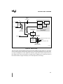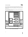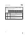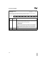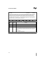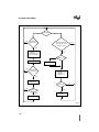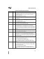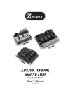
1
87C196CB Supplement to
8XC196NT User’s Manual
CB_title.fm5 Page 1 Tuesday, September 15, 1998 9:54 AM
87C196CB Supplement to
8XC196NT User’s Manual
August 2004
Order Number: 272787-003
CB_legal.fm5 Page 1 Tuesday, September 15, 1998 9:39 AM
Information in this document is provided in connection with Intel products. No license, express or implied, by estoppel or
otherwise, to any intellectual property rights is granted by this document. Except as provided in Intel’s Terms and Conditions
of Sale for such products, Intel assumes no liability whatsoever, and Intel disclaims any express or implied warranty, relating
to sale and/or use of Intel products including liability or warranties relating to fitness for a particular purpose, merchantability,
or infringement of any patent, copyright or other intellectual property right. Intel products are not intended for use in medical,
life saving, or life sustaining applications.
Intel may make changes to specifications and product descriptions at any time, without notice.
Designers must not rely on the absence or characteristics of any features or instructions marked "reserved" or "undefined."
Intel reserves these for future definition and shall have no responsibility whatsoever for conflicts or incompatibilities arisin g
from future changes to them.
The 87C196CB and 8XC196NT microprocessors may contain design defects or errors known as errata which may cause the
products to deviate from published specifications. Current characterized errata are available on request.
Contact your local Intel sales office or your distributor to obtain the latest specifications and before placing your product order.
Copies of documents which have an ordering number and are referenced in this document, or other Intel literature may be
obtained by calling 1-800-548-4725 or by visiting Intel’s website at http://www.intel.com.
Copyright © Intel Corporation, 1998, 2004
*Third-party brands and names are the property of their respective owners.
CONTENTS
CHAPTER 1
GUIDE TO THIS MANUAL
1.1
MANUAL CONTENTS ................................................................................................... 1-1
1.2
RELATED DOCUMENTS .............................................................................................. 1-2
CHAPTER 2
ARCHITECTURAL OVERVIEW
2.1
DEVICE FEATURES ..................................................................................................... 2-1
2.2
BLOCK DIAGRAM ......................................................................................................... 2-2
2.3
INTERNAL TIMING........................................................................................................ 2-2
CHAPTER 3
MEMORY PARTITIONS
3.1
MEMORY MAP, SPECIAL-FUNCTION REGISTERS, AND WINDOWING .................. 3-1
CHAPTER 4
STANDARD AND PTS INTERRUPTS
4.1
INTERRUPT SOURCES, VECTORS, AND PRIORITIES ............................................. 4-1
CHAPTER 5
I/O PORTS
5.1
PORT 0 AND EPORT .................................................................................................... 5-1
CHAPTER 6
ANALOG-TO-DIGITAL (A/D) CONVERTER
6.1
ADDITIONAL A/D INPUT CHANNELS .......................................................................... 6-1
CHAPTER 7
CAN SERIAL COMMUNICATIONS CONTROLLER
7.1
CAN FUNCTIONAL OVERVIEW ................................................................................... 7-1
7.2
CAN CONTROLLER SIGNALS AND REGISTERS....................................................... 7-3
7.3
CAN CONTROLLER OPERATION................................................................................ 7-4
7.3.1
Address Map .............................................................................................................7-5
7.3.2
Message Objects ......................................................................................................7-5
7.3.2.1
Receive and Transmit Priorities ...........................................................................7-6
7.3.2.2
Message Acceptance Filtering .............................................................................7-6
7.3.3
Message Frames ......................................................................................................7-7
7.3.4
Error Detection and Management Logic ...................................................................7-9
7.3.5
Bit Timing ................................................................................................................7-10
7.3.5.1
Bit Timing Equations ..........................................................................................7-12
7.4
CONFIGURING THE CAN CONTROLLER ................................................................. 7-13
7.4.1
Programming the CAN Control (CAN_CON) Register ............................................7-13
7.4.2
Programming the Bit Timing 0 (CAN_BTIME0) Register ........................................7-15
7.4.3
Programming the Bit Timing 1 (CAN_BTIME1) Register ........................................7-16
iii
87C196CB SUPPLEMENT
7.4.4
Programming a Message Acceptance Filter ...........................................................7-17
7.5
CONFIGURING MESSAGE OBJECTS ....................................................................... 7-20
7.5.1
Specifying a Message Object’s Configuration .........................................................7-21
7.5.2
Programming the Message Object Identifier ...........................................................7-22
7.5.3
Programming the Message Object Control Registers .............................................7-23
7.5.3.1
Message Object Control Register 0 ...................................................................7-23
7.5.3.2
Message Object Control Register 1 ...................................................................7-23
7.5.4
Programming the Message Object Data .................................................................7-23
7.6
ENABLING THE CAN INTERRUPTS .......................................................................... 7-29
7.7
DETERMINING THE CAN CONTROLLER’S INTERRUPT STATUS ......................... 7-32
7.8
FLOW DIAGRAMS ...................................................................................................... 7-35
7.9
DESIGN CONSIDERATIONS...................................................................................... 7-41
7.9.1
Hardware Reset ......................................................................................................7-41
7.9.2
Software Initialization ..............................................................................................7-41
7.9.3
Bus-off State ...........................................................................................................7-41
CHAPTER 8
SPECIAL OPERATING MODES
8.1
CLOCK CIRCUITRY ...................................................................................................... 8-1
CHAPTER 9
INTERFACING WITH EXTERNAL MEMORY
9.1
ADDRESS PINS ............................................................................................................ 9-1
9.2
BUS TIMING MODES.................................................................................................... 9-1
CHAPTER 10
PROGRAMMING THE NONVOLATILE MEMORY
10.1 SIGNATURE WORD AND PROGRAMMING VOLTAGES.......................................... 10-1
10.2 MEMORY MAP FOR SLAVE PROGRAMMING MODE .............................................. 10-1
10.3 MEMORY MAP AND CIRCUIT FOR AUTO PROGRAMMING ................................... 10-2
10.4 MEMORY MAP FOR SERIAL PORT PROGRAMMING.............................................. 10-3
10.4.1 Selecting Bank 0 (FF2000–FF7FFFH) ....................................................................10-4
10.4.2 Selecting Bank 1 (FF8000–FFFFFFH) ....................................................................10-4
APPENDIX A
SIGNAL DESCRIPTIONS
A.1
FUNCTIONAL GROUPINGS OF SIGNALS ................................................................. A-1
A.2
SIGNAL DESCRIPTIONS............................................................................................. A-3
A.3
DEFAULT CONDITIONS ............................................................................................ A-14
GLOSSARY
INDEX
iv
CONTENTS
FIGURES
Figure
2-1
2-2
2-3
2-4
4-1
4-2
5-1
5-2
5-3
5-4
5-5
6-1
6-2
7-1
7-2
7-3
7-4
7-5
7-6
7-7
7-8
7-9
7-10
7-11
7-12
7-13
7-14
7-15
7-16
7-17
7-18
7-19
7-20
7-21
7-22
7-23
7-24
7-25
7-26
8-1
9-1
9-2
10-1
A-1
Page
87C196CB Block Diagram............................................................................................2-2
Clock Circuitry ..............................................................................................................2-3
Internal Clock Phases ..................................................................................................2-4
Effect of Clock Mode on CLKOUT Frequency..............................................................2-5
Interrupt Mask 1 (INT_MASK1) Register......................................................................4-2
interrupt Pending 1 (INT_PEND1) Register..................................................................4-2
Port x Pin Input (Px_PIN) Register ...............................................................................5-1
Extended Port I/O Direction (EP_DIR) Register ...........................................................5-2
Extended Port Mode (EP_MODE) Register .................................................................5-2
Extended Port Input (EP_PIN) Register .......................................................................5-3
Extended Port Data Output (EP_REG) Register ..........................................................5-3
A/D Command (AD_COMMAND) Register ..................................................................6-2
A/D Result (AD_RESULT) Register — Read Format...................................................6-3
A System Using CAN Controllers .................................................................................7-1
CAN Controller Block Diagram .....................................................................................7-2
CAN Message Frames .................................................................................................7-7
A Bit Time as Specified by the CAN Protocol.............................................................7-10
A Bit Time as Implemented in the CAN Controller .....................................................7-11
CAN Control (CAN_CON) Register ............................................................................7-13
CAN Bit Timing 0 (CAN_BTIME0) Register................................................................7-15
CAN Bit Timing 1 (CAN_BTIME1) Register................................................................7-16
CAN Standard Global Mask (CAN_SGMSK) Register ...............................................7-18
CAN Extended Global Mask (CAN_EGMSK) Register ..............................................7-19
CAN Message 15 Mask (CAN_MSK15) Register.......................................................7-20
CAN Message Object x Configuration (CAN_MSGxCFG) Register...........................7-21
CAN Message Object x Identifier (CAN_MSGxID0–3) Register ................................7-22
CAN Message Object x Control 0 (CAN_MSGxCON0) Register ...............................7-24
CAN Message Object x Control 1 (CAN_MSGxCON1) Register ...............................7-26
CAN Message Object Data (CAN_MSGxDATA0–7) Registers..................................7-28
CAN Control (CAN_CON) Register ............................................................................7-29
CAN Message Object x Control 0 (CAN_MSGxCON0) Register ...............................7-31
CAN Interrupt Pending (CAN_INT) Register ..............................................................7-32
CAN Status (CAN_STAT) Register ............................................................................7-33
CAN Message Object x Control 0 (CAN_MSGxCON0) Register ...............................7-34
Receiving a Message for Message Objects 1–14 — CPU Flow ................................7-36
Receiving a Message for Message Object 15 — CPU Flow ......................................7-37
Receiving a Message — CAN Controller Flow...........................................................7-38
Transmitting a Message — CPU Flow .......................................................................7-39
Transmitting a Message — CAN Controller Flow.......................................................7-40
Clock Circuitry ..............................................................................................................8-1
Modes 0 and 3 Timings ................................................................................................9-2
Chip Configuration 1 (CCR1) Register .........................................................................9-3
Auto Programming Circuit ..........................................................................................10-3
87C196CB 84-pin PLCC Package .............................................................................. A-2
v
8XC196CB SUPPLEMENT
FIGURES
Figure
Page
A-2
87C196CB 100-pin QFP Package .............................................................................. A-3
vi
CONTENTS
TABLES
Table
1-1
2-1
2-2
2-3
3-1
3-2
3-3
3-4
3-5
3-6
3-7
3-8
3-9
4-1
5-1
6-1
7-1
7-2
7-3
7-4
7-5
7-6
7-7
7-8
7-9
7-10
7-11
7-12
7-13
7-14
9-1
10-1
10-2
10-3
10-4
A-1
A-2
A-3
A-4
A-5
Page
Related Documents ......................................................................................................1-2
Features of the 8XC196NT and 87C196CB .................................................................2-1
State Times at Various Frequencies ............................................................................2-4
Relationships Between Input Frequency, Clock Multiplier, and State Times ...............2-5
Register File Memory Addresses .................................................................................3-1
87C196CB Memory Map ..............................................................................................3-2
87C196CB Peripheral SFRs.........................................................................................3-3
CAN Peripheral SFRs...................................................................................................3-4
Selecting a Window of Peripheral SFRs.......................................................................3-6
Selecting a Window of the Upper Register File ............................................................3-7
Selecting a Window of Upper Register RAM................................................................3-8
Windows .......................................................................................................................3-9
WSR Settings and Direct Addresses for Windowable SFRs ......................................3-11
Interrupt Sources, Vectors, and Priorities.....................................................................4-1
87C196CB Input/Output Ports......................................................................................5-1
A/D Converter Pins.......................................................................................................6-1
CAN Controller Signals.................................................................................................7-3
Control and Status Registers .......................................................................................7-3
CAN Controller Address Map .......................................................................................7-5
Message Object Structure ............................................................................................7-6
Effect of Masking on Message Identifiers.....................................................................7-7
Standard Message Frame ............................................................................................7-8
Extended Message Frame ...........................................................................................7-8
CAN Protocol Bit Time Segments ..............................................................................7-10
CAN Controller Bit Time Segments ............................................................................7-11
Bit Timing Relationships.............................................................................................7-12
Bit Timing Requirements for Synchronization ............................................................7-17
Control Register Bit-pair Interpretation .......................................................................7-23
Cross-reference for Register Bits Shown in Flowcharts .............................................7-35
Register Values Following Reset................................................................................7-41
Modes 0 and 3 Timing Comparisons............................................................................9-1
Signature Word and Programming Voltages ..............................................................10-1
Slave Programming Mode Memory Map ....................................................................10-2
Auto Programming Memory Map................................................................................10-2
Serial Port Programming Mode Memory Map ............................................................10-4
87C196CB Signals Arranged by Functional Categories.............................................. A-1
Description of Columns of Table A-3........................................................................... A-4
Signal Descriptions...................................................................................................... A-4
Definition of Status Symbols ..................................................................................... A-14
87C196CB Pin Status ............................................................................................... A-14
vii
1
Guide to This Manual
CHAPTER 1
GUIDE TO THIS MANUAL
This document is a supplement to the 8XC196NT Microcontroller User’s Manual. It describes
the differences between the 87C196CB and the 8XC196NT. For information not found in this
supplement, please consult the 8XC196NT Microcontroller User’s Manual (order number
272317) or the 87C196CB datasheet (87C196CA/87C196CB 20 MHz Advanced 16-Bit CHMOS
Microcontroller with Integrated CAN 2.0, order number 272405).
1.1
MANUAL CONTENTS
This supplement contains several chapters, an appendix, a glossary, and an index. This chapter,
Chapter 1, provides an overview of the supplement. This section summarizes the contents of the
remaining chapters and appendixes. The remainder of this chapter provides references to related
documentation.
Chapter 2 — Architectural Overview — compares the features of the 87C196CB with those of
the 8XC196NT and describes the 87C196CB’s internal clock circuitry.
Chapter 3 — Memory Partitions — describes the addressable memory space of the 84-pin and
100-pin 87C196CB, lists the peripheral special-function registers (SFRs), and provides tables of
WSR values for windowing higher memory into the lower register file for direct access.
Chapter 4 — Standard and PTS Interrupts — describes the additional interrupts for the CAN
(controller area network) peripheral and the SFRs that support those interrupts.
Chapter 5 — I/O Ports — describes the port 0 and EPORT differences for the 100-pin
87C196CB. Both port 0 and the EPORT are implemented as eight-bit ports on the 100-pin
87C196CB, but as four-bit ports (like the 8XC196NT) on the 84-pin 87C196CB.
Chapter 6 — Analog-to-digital (A/D) Converter — illustrates the SFRs that are affected by the
implementation of port 0 as an eight-bit port.
Chapter 7 — CAN Serial Communications Controller — describes the 87C196CB’s integrated CAN controller and explains how to configure it. This integrated peripheral is similar to Intel’s
standalone 82527 CAN serial communications controller, supporting both the standard and extended message frames specified by the CAN 2.0 protocol parts A and B.
Chapter 8 — Special Operating Modes — illustrates the clock control circuitry of the
87C196CB.
1-1
87C196CB SUPPLEMENT
Chapter 9 — Interfacing with External Memory — discusses differences in the bus timing
modes supported by the 8XC196NT and the 87C196CB.
Chapter 10 — Programming the Nonvolatile Memory — describes the memory maps and recommended circuits to support programming of the 87C196CB’s 56 Kbytes of OTPROM.
Appendix A — Signal Descriptions — describes the additional signals implemented on the
87C196CB.
Glossary — defines terms with special meaning used throughout this supplement.
Index — lists key topics with page number references.
1.2
RELATED DOCUMENTS
Table 1-1 lists additional documents that you may find useful in designing systems incorporating
the 87C196CB microcontroller.
Table 1-1. Related Documents
Title and Description
8XC196NT Microcontroller User’s Manual
Automotive Products handbook
87C196CB 20 MHz Advanced 16-Bit CHMOS Microcontroller with
Integrated CAN 2.0 (datasheet)
1-2
Order Number
272317
231792
272405
2
Architectural
Overview
CHAPTER 2
ARCHITECTURAL OVERVIEW
This chapter describes architectural differences between the 87C196CB and the 8XC196NT.
Both the 8XC196NT and the 87C196CB are designed for high-speed calculations and fast I/O.
With the addition of the CAN (controller area network) peripheral, the 87C196CB reduces pointto-point wiring requirements, making it well-suited to automotive and factory automation applications.
The 87C196CB is available in either an 84-pin or a 100-pin package. The 84-pin 87C196CB, like
the 8XC196NT, has up to 20 external address lines, enabling access to 1 Mbyte of linear address
space. The 100-pin 87C196CB has four additional pins available for external address lines. With
all 24 external address lines connected, the 100-pin 87C196CB can access 16 Mbytes of linear
address space.
2.1
DEVICE FEATURES
Table 2-1 lists the features of the 8XC196NT and the 87C196CB. The 87C196CB implements
more OTPROM, more register RAM, four additional A/D channels, and the CAN peripheral. The
100-pin 87C196CB also implements four additional EPORT pins.
Table 2-1. Features of the 8XC196NT and 87C196CB
8XC196NT
68
0 or 32 K
1K
512
56
10
2
4
1
4
0
87C196CB
84
56 K
1.5 K
512
56
10
2
8
1
4
2
87C196CB
100
56 K
1.5 K
512
60
10
2
8
1
8
2
†
Register RAM amount includes the 24 bytes allocated to the core SFRs and stack pointer.
2-1
87C196CB SUPPLEMENT
2.2
BLOCK DIAGRAM
Figure 2-1 shows the major blocks within the device. The 8XC196NT and 87C196CB have the
same peripheral set with the exception of the CAN (controller area network) peripheral, which is
unique to the 87C196CB. The CAN peripheral manages communications between multiple network nodes. This integrated peripheral is similar to Intel’s standalone 82527 CAN serial communications controller, supporting both the standard and extended message frames specified by the
CAN 2.0 protocol parts A and B.
I/O
Core
OTPROM
Interrupt
Controller
Clock and
Power Mgmt.
Code/Data
RAM
PTS
SIO
SSIO
EPA
A/D
WDT
Slave
Port
CAN
A3179-01
Figure 2-1. 87C196CB Block Diagram
2.3
INTERNAL TIMING
The 87C196CB’s clock circuitry (Figure 2-2) implements phase-locked loop and clock multiplier
circuitry, which can substantially increase the CPU clock rate while using a lower-frequency input clock. The clock circuitry accepts an input clock signal on XTAL1 provided by an external
crystal or oscillator. Depending on the value of the PLLEN pin, this frequency is routed either
through the phase-locked loop and multiplier or directly to the divide-by-two circuit. The multiplier circuitry can quadruple the input frequency (FXTAL1) before the frequency (f) reaches the divide-by-two circuitry. The clock generators accept the divided input frequency (f/2) from the
divide-by-two circuit and produce two nonoverlapping internal timing signals, PH1 and PH2.
These signals are active when high.
NOTE
This manual uses lowercase “f” to represent the internal clock frequency. For
the 87C196CB, f is equal to either FXTAL1 or 4FXTAL1, depending on the clock
multiplier mode, which is controlled by the PLLEN input pin.
2-2
ARCHITECTURAL OVERVIEW
Disable
PLL
(Powerdown)
FXTAL1
Phase
Comparator
FXTAL1
XTAL1
Disable
Oscillator
(Powerdown)
Phaselocked
Oscillator
4FXTAL1
XTAL2
Disable Clock Input
(Powerdown)
f
PLLEN
Filter
Phase-locked Loop
Clock Multiplier
Divide-by-two
Circuit
f
2
Disable Clocks
(Powerdown)
Peripheral Clocks (PH1, PH2)
Clock
Generators
CLKOUT
CPU Clocks (PH1, PH2)
Disable Clocks
(Idle, Powerdown)
A3168-01
Figure 2-2. Clock Circuitry
The rising edges of PH1 and PH2 generate the internal CLKOUT signal (Figure 2-3). The clock
circuitry routes separate internal clock signals to the CPU and the peripherals to provide flexibility in power management. It also outputs the CLKOUT signal on the CLKOUT pin. Because of
the complex logic in the clock circuitry, the signal on the CLKOUT pin is a delayed version of
the internal CLKOUT signal. This delay varies with temperature and voltage.
2-3
87C196CB SUPPLEMENT
XTAL1
t
t
1 State Time
1 State Time
PH1
PH2
CLKOUT
Phase 1
Phase 2
Phase 1
Phase 2
A0805-01
Figure 2-3. Internal Clock Phases
The combined period of phase 1 and phase 2 of the internal CLKOUT signal defines the basic
time unit known as a state time or state. Table 2-2 lists state time durations at various frequencies.
Table 2-2. State Times at Various Frequencies
f
(Frequency Input to the
Divide-by-two Circuit)
State Time
8 MHz
250 ns
12 MHz
167 ns
16 MHz
125 ns
20 MHz
100 ns
The following formulas calculate the frequency of PH1 and PH2, the duration of a state time, and
the duration of a clock period (t).
f
PH1 (in MHz) = --- = PH2
2
2
State Time (in µs) = --f
1
t = --f
Because the device can operate at many frequencies, this manual defines time requirements (such
as instruction execution times) in terms of state times rather than specific measurements.
Datasheets list AC characteristics in terms of clock periods (t; sometimes called Tosc).
Figure 2-4 illustrates the timing relationships between the input frequency (FXTAL1), the operating
frequency (f), and the CLKOUT signal with each PLLEN pin configuration. Table 2-3 details the
relationships between the input frequency (FXTAL1), the PLLEN pin, the operating frequency (f),
the clock period (t), and state times.
2-4
ARCHITECTURAL OVERVIEW
PLLEN = 0
XTAL1 (5 MHz)
t = 80ns
f
TXHCH
CLKOUT
PLLEN = 1
XTAL1 (5 MHz)
t = 20ns
f
TXHCH
CLKOUT
A3170-01
Figure 2-4. Effect of Clock Mode on CLKOUT Frequency
Table 2-3. Relationships Between Input Frequency, Clock Multiplier, and State Times
FXTAL1
(Frequency
on XTAL1)
PLLEN
Multiplier
f
(Input Frequency to
the Divide-by-two Circuit)
t
(Clock
Period)
State Time
4 MHz
0
1
4 MHz
250 ns
500 ns
5 MHz
0
1
5 MHz
200 ns
400 ns
8 MHz
0
1
8 MHz
125 ns
250 ns
12 MHz
0
1
12 MHz
83.5 ns
167 ns
16 MHz
0
1
16 MHz
62.5 ns
125 ns
20 MHz
0
1
20 MHz
50 ns
100 ns
4 MHz
1
4
16 MHz
62.5 ns
125 ns
5 MHz
1
4
20 MHz
50 ns
100 ns
2-5
3
Memory Partitions
CHAPTER 3
MEMORY PARTITIONS
This chapter describes the differences in the address space of the 87C196CB from that of the
8XC196NT. The 87C196CB has 56 Kbytes of one-time-programmable read-only memory (OTPROM), while the 8XC196NT is available with 32 Kbytes. The 87C196CB also has an additional
512 bytes of register RAM.
The 87C196CB is available in either an 84-pin or a 100-pin package. The 84-pin 87C196CB, like
the 8XC196NT, has up to 20 external address lines, enabling access to 1 Mbyte of linear address
space. The 100-pin 87C196CB has four additional pins available for external address lines. With
all 24 external address lines connected (A23:16 and AD15:0), the 100-pin 87C196CB can access
16 Mbytes of linear address space.
3.1
MEMORY MAP, SPECIAL-FUNCTION REGISTERS, AND WINDOWING
Table 3-1 compares the register file addresses of the 8XC196NT and 87C196CB. Table 3-2 is a
memory map of the 87C196CB. Table 3-3 lists the 87C196CB’s peripheral SFRs (these are the
same as those of the 8XC196NT). Table 3-4 lists the CAN peripheral SFRs, which are unique to
the 87C196CB. Tables 3-5 through 3-9 provide the information necessary to window higher
memory into the lower register file for direct access.
Table 3-1. Register File Memory Addresses
Device and Hex
Address Range
CB
NT
1DFF
1C00
—
03FF
0100
Description
Addressing Modes
Register RAM
Indirect, indexed, or windowed direct
03FF
0100
Upper register file (register RAM)
Indirect, indexed, or windowed direct
00FF
001A
00FF
001A
Lower register file (register RAM)
Direct, indirect, or indexed
0019
0018
0019
0018
Lower register file (stack pointer)
Direct, indirect, or indexed
0017
0000
0017
0000
Lower register file (CPU SFRs)
Direct, indirect, or indexed
.
.
3-1
87C196CB SUPPLEMENT
Table 3-2. 87C196CB Memory Map
Hex
Address
Description
Addressing Modes
FFFFFF
FF2080
Program memory (After a device reset, the first instruction fetch
is from FF2080H) †
Indirect, indexed, extended
FF207F
FF2000
Special purpose memory †
Indirect, indexed, extended
FF1FFF
FF0600
External device (memory or I/O) connected to address/data bus
Indirect, indexed, extended
FF05FF
FF0400
Internal code and data RAM
(mapped identically into pages FFH and 00H)
Indirect, indexed, extended
FF03FF
FF0100
External device (memory or I/O) connected to address/data bus
Indirect, indexed, extended
FF00FF
FF0000
Reserved ††
Indirect, indexed, extended
FEFFFF
0F0000
100-pin 87C196CB: External device (memory or I/O)
84-pin 87C196CB: Overlaid memory ††
Indirect, indexed, extended
0EFFFF
010000
External device (memory or I/O) connected to address/data bus
Indirect, indexed, extended
00FFFF
002000
External device or remapped OTPROM †††
Indirect, indexed, extended
001FFF
001FE0
Memory-mapped SFRs
Indirect, indexed, extended
001FDF
001F00
Peripheral SFRs
Indirect, indexed, extended,
windowed direct
001EFF
001E00
CAN SFRs
Indirect, indexed, extended
001DFF
001C00
Internal register RAM
001BFF
000600
External device (memory or I/O) connected to address/data bus;
future SFR expansion
Indirect, indexed, extended
0005FF
000400
Internal code and data RAM
(mapped identically into pages 00H and FFH)
Indirect, indexed, extended
0003FF
000100
Upper register file (register RAM)
0000FF
000000
Lower register file (register RAM, stack pointer, CPU SFRs)
Indirect, indexed,
windowed direct
Indirect, indexed,
windowed direct
Direct, indirect, indexed
† For the 87C196CB, the program and special-purpose memory locations (FF2000-FFFFFFH) can reside
either in external memory or in internal OTPROM.
††
Locations xF0000-xF00FFH are reserved for in-circuit emulators. Do not use these locations except to
initialize them. Except as otherwise noted, initialize unused program memory locations and reserved
memory locations to FFH.
†††
3-2
These locations can be either external memory (CCB2.2=0) or a copy of the OTPROM (CCB2.2=1).
MEMORY PARTITIONS
Table 3-3. 87C196CB Peripheral SFRs
Ports 0, 1, 2, and 6 SFRs
Address
High (Odd) Byte
Low (Even) Byte
Reserved
Timer 1, Timer 2, and EPA SFRs
Address
†1F9EH
High (Odd) Byte
TIMER2 (H)
Low (Even) Byte
1FDEH
Reserved
TIMER2 (L)
1FDCH
Reserved
Reserved
1F9CH
Reserved
T2CONTROL
1FDAH
Reserved
P0_PIN
†1F9AH
TIMER1 (H)
TIMER1 (L)
1FD8H
Reserved
Reserved
1F98H
Reserved
T1CONTROL
1FD6H
P6_PIN
P1_PIN
1F96H
Reserved
Reserved
1FD4H
P6_REG
P1_REG
1F94H
Reserved
Reserved
1FD2H
P6_DIR
P1_DIR
1F92H
Reserved
Reserved
1FD0H
P6_MODE
P1_MODE
1F90H
Reserved
Reserved
1FCEH
P2_PIN
Reserved
EPA SFRs
1FCCH
P2_REG
Reserved
Address
High (Odd) Byte
Low (Even) Byte
1FCAH
P2_DIR
Reserved
†1F8EH
COMP1_TIME (H)
COMP1_TIME (L)
1FC8H
P2_MODE
Reserved
1F8CH
Reserved
COMP1_CON
1FC6H
Reserved
Reserved
†1F8AH
COMP0_TIME (H)
COMP0_TIME (L)
1FC4H
Reserved
Reserved
1F88H
Reserved
COMP0_CON
1FC2H
Reserved
Reserved
†1F86H
EPA9_TIME (H)
EPA9_TIME (L)
1FC0H
Reserved
Reserved
SIO and SSIO SFRs
Address
High (Odd) Byte
Low (Even) Byte
1F84H
Reserved
EPA9_CON
†1F82H
EPA8_TIME (H)
EPA8_TIME (L)
Reserved
EPA8_CON
1F80H
1FBEH
Reserved
Reserved
†1F7EH
EPA7_TIME (H)
EPA7_TIME (L)
1FBCH
SP_BAUD (H)
SP_BAUD (L)
1F7CH
Reserved
EPA7_CON
1FBAH
SP_CON
SBUF_TX
†1F7AH
EPA6_TIME (H)
EPA6_TIME (L)
1FB8H
SP_STATUS
SBUF_RX
1F78H
Reserved
EPA6_CON
1FB6H
Reserved
Reserved
†1F76H
EPA5_TIME (H)
EPA5_TIME (L)
1FB4H
Reserved
SSIO_BAUD
1F74H
Reserved
EPA5_CON
1FB2H
SSIO1_CON
SSIO1_BUF
†1F72H
EPA4_TIME (H)
EPA4_TIME (L)
1FB0H
SSIO0_CON
SSIO0_BUF
Address
High (Odd) Byte
Low (Even) Byte
1FAEH
AD_TIME
AD_TEST
1FACH
Reserved
AD_COMMAND
1FAAH
AD_RESULT (H)
AD_RESULT (L)
EPA Interrupt SFRs
Address
High (Odd) Byte
Low (Even) Byte
1FA8H
Reserved
EPAIPV
1FA6H
Reserved
EPA_PEND1
1FA4H
Reserved
EPA_MASK1
†1FA2H
EPA_PEND (H)
EPA_PEND (L)
†1FA0H
EPA_MASK (H)
EPA_MASK (L)
†
1F70H
†1F6EH
A/D SFRs
Reserved
EPA4_CON
EPA3_TIME (H)
EPA3_TIME (L)
†1F6CH
EPA3_CON (H)
EPA3_CON (L)
†1F6AH
EPA2_TIME (H)
EPA2_TIME (L)
1F68H
Reserved
EPA2_CON
†1F66H
EPA1_TIME (H)
EPA1_TIME (L)
†1F64H
EPA1_CON (H)
EPA1_CON (L)
†1F62H
EPA0_TIME (H)
EPA0_TIME (L)
1F60H
Reserved
EPA0_CON
Must be addressed as a word.
3-3
87C196CB SUPPLEMENT
Table 3-4. CAN Peripheral SFRs
Message 15
Addr
High (Odd) Byte
Message 11
Low (Even) Byte
Addr
CAN_MSG15DATA7
1EBEH
High (Odd) Byte
Reserved
Low (Even) Byte
1EFEH
Reserved
1EFCH
CAN_MSG15DATA6
CAN_MSG15DATA5
1EBCH
CAN_MSG11DATA6
CAN_MSG11DATA5
1EFAH
CAN_MSG15DATA4
CAN_MSG15DATA3
1EBAH
CAN_MSG11DATA4
CAN_MSG11DATA3
1EF8H
CAN_MSG15DATA2
CAN_MSG15DATA1
1EB8H
CAN_MSG11DATA2
CAN_MSG11DATA1
1EF6H
CAN_MSG15DATA0
CAN_MSG15CFG
1EB6H
CAN_MSG11DATA0
CAN_MSG11CFG
1EF4H
CAN_MSG15ID3
CAN_MSG15ID2
1EB4H
CAN_MSG11ID3
CAN_MSG11ID2
1EF2H
CAN_MSG15ID1
CAN_MSG15ID0
1EB2H
CAN_MSG11ID1
CAN_MSG11ID0
1EF0H
CAN_MSG15CON1
CAN_MSG15CON0
1EB0H
CAN_MSG11CON1
CAN_MSG11CON0
Message 14
Addr
High (Odd) Byte
CAN_MSG11DATA7
Message 10
Low (Even) Byte
Addr
1EEEH
Reserved
CAN_MSG14DATA7
1EAEH
Reserved
High (Odd) Byte
CAN_MSG10DATA7
1EECH
CAN_MSG14DATA6
CAN_MSG14DATA5
1EACH
CAN_MSG10DATA6
CAN_MSG10DATA5
1EEAH
CAN_MSG14DATA4
CAN_MSG14DATA3
1EAAH
CAN_MSG10DATA4
CAN_MSG10DATA3
1EE8H
CAN_MSG14DATA2
CAN_MSG14DATA1
1EA8H
CAN_MSG10DATA2
CAN_MSG10DATA1
1EE6H
CAN_MSG14DATA0
CAN_MSG14CFG
1EA6H
CAN_MSG10DATA0
CAN_MSG10CFG
1EE4H
CAN_MSG14ID3
CAN_MSG14ID2
1EA4H
CAN_MSG10ID3
CAN_MSG10ID2
1EE2H
CAN_MSG14ID1
CAN_MSG14ID0
1EA2H
CAN_MSG10ID1
CAN_MSG10ID0
1EE0H
CAN_MSG14CON1
CAN_MSG14CON0
1EA0H
CAN_MSG10CON1
CAN_MSG10CON0
Message 13
Addr
1EDEH
High (Odd) Byte
Reserved
Low (Even) Byte
Message 9
Low (Even) Byte
Addr
CAN_MSG13DATA7
1E9EH
High (Odd) Byte
Reserved
Low (Even) Byte
CAN_MSG9DATA7
1EDCH
CAN_MSG13DATA6
CAN_MSG13DATA5
1E9CH
CAN_MSG9DATA6
CAN_MSG9DATA5
1EDAH
CAN_MSG13DATA4
CAN_MSG13DATA3
1E9AH
CAN_MSG9DATA4
CAN_MSG9DATA3
1ED8H
CAN_MSG13DATA2
CAN_MSG13DATA1
1E98H
CAN_MSG9DATA2
CAN_MSG9DATA1
1ED6H
CAN_MSG13DATA0
CAN_MSG13CFG
1E96H
CAN_MSG9DATA0
CAN_MSG9CFG
1ED4H
CAN_MSG13ID3
CAN_MSG13ID2
1E94H
CAN_MSG9ID3
CAN_MSG9ID2
1ED2H
CAN_MSG13ID1
CAN_MSG13ID0
1E92H
CAN_MSG9ID1
CAN_MSG9ID0
1ED0H
CAN_MSG13CON1
CAN_MSG13CON0
1E90H
CAN_MSG9CON1
CAN_MSG9CON0
Message 12
Addr
1ECEH
High (Odd) Byte
Reserved
Message 8
Low (Even) Byte
Addr
CAN_MSG12DATA7
1E8EH
High (Odd) Byte
Reserved
Low (Even) Byte
CAN_MSG8DATA7
1ECCH
CAN_MSG12DATA6
CAN_MSG12DATA5
1E8CH
CAN_MSG8DATA6
CAN_MSG8DATA5
1ECAH
CAN_MSG12DATA4
CAN_MSG12DATA3
1E8AH
CAN_MSG8DATA4
CAN_MSG8DATA3
1EC8H
CAN_MSG12DATA2
CAN_MSG12DATA1
1E88H
CAN_MSG8DATA2
CAN_MSG8DATA1
1EC6H
CAN_MSG12DATA0
CAN_MSG12CFG
1E86H
CAN_MSG8DATA0
CAN_MSG8CFG
1EC4H
CAN_MSG12ID3
CAN_MSG12ID2
1E84H
CAN_MSG8ID3
CAN_MSG8ID2
1EC2H
CAN_MSG12ID1
CAN_MSG12ID0
1E82H
CAN_MSG8ID1
CAN_MSG8ID0
1EC0H
CAN_MSG12CON1
CAN_MSG12CON0
1E80H
CAN_MSG8CON1
CAN_MSG8CON0
3-4
MEMORY PARTITIONS
Table 3-4. CAN Peripheral SFRs (Continued)
Message 7
Addr
1E7EH
High (Odd) Byte
Reserved
Message 3 and Bit Timing 0
Low (Even) Byte
Addr
CAN_MSG7DATA7
1E3EH
High (Odd) Byte
CAN_BTIME0†
Low (Even) Byte
CAN_MSG3DATA7
1E7CH
CAN_MSG7DATA6
CAN_MSG7DATA5
1E3CH
CAN_MSG3DATA6
CAN_MSG3DATA5
1E7AH
CAN_MSG7DATA4
CAN_MSG7DATA3
1E3AH
CAN_MSG3DATA4
CAN_MSG3DATA3
1E78H
CAN_MSG7DATA2
CAN_MSG7DATA1
1E38H
CAN_MSG3DATA2
CAN_MSG3DATA1
1E76H
CAN_MSG7DATA0
CAN_MSG7CFG
1E36H
CAN_MSG3DATA0
CAN_MSG3CFG
1E74H
CAN_MSG7ID3
CAN_MSG7ID2
1E34H
CAN_MSG3ID3
CAN_MSG3ID2
1E72H
CAN_MSG7ID1
CAN_MSG7ID0
1E32H
CAN_MSG3ID1
CAN_MSG3ID0
1E70H
CAN_MSG7CON1
CAN_MSG7CON0
1E30H
CAN_MSG3CON1
CAN_MSG3CON0
Message 6
Addr
1E6EH
High (Odd) Byte
Reserved
Message 2
Low (Even) Byte
Addr
CAN_MSG6DATA7
1E2EH
High (Odd) Byte
Reserved
Low (Even) Byte
CAN_MSG2DATA7
1E6CH
CAN_MSG6DATA6
CAN_MSG6DATA5
1E2CH
CAN_MSG2DATA6
CAN_MSG2DATA5
1E6AH
CAN_MSG6DATA4
CAN_MSG6DATA3
1E2AH
CAN_MSG2DATA4
CAN_MSG2DATA3
1E68H
CAN_MSG6DATA2
CAN_MSG6DATA1
1E28H
CAN_MSG2DATA2
CAN_MSG2DATA1
1E66H
CAN_MSG6DATA0
CAN_MSG6CFG
1E26H
CAN_MSG2DATA0
CAN_MSG2CFG
1E64H
CAN_MSG6ID3
CAN_MSG6ID2
1E24H
CAN_MSG2ID3
CAN_MSG2ID2
1E62H
CAN_MSG6ID1
CAN_MSG6ID0
1E22H
CAN_MSG2ID1
CAN_MSG2ID0
1E60H
CAN_MSG6CON1
CAN_MSG6CON0
1E20H
CAN_MSG2CON1
CAN_MSG2CON0
Message 5 and Interrupts
Addr
1E5EH
High (Odd) Byte
CAN_INT
Low (Even) Byte
Message 1
Addr
CAN_MSG5DATA7
1E1EH
High (Odd) Byte
Reserved
Low (Even) Byte
CAN_MSG1DATA7
1E5CH
CAN_MSG5DATA6
CAN_MSG5DATA5
1E1CH
CAN_MSG1DATA6
CAN_MSG1DATA5
1E5AH
CAN_MSG5DATA4
CAN_MSG5DATA3
1E1AH
CAN_MSG1DATA4
CAN_MSG1DATA3
1E58H
CAN_MSG5DATA2
CAN_MSG5DATA1
1E18H
CAN_MSG1DATA2
CAN_MSG1DATA1
1E56H
CAN_MSG5DATA0
CAN_MSG5CFG
1E16H
CAN_MSG1DATA0
CAN_MSG1CFG
1E54H
CAN_MSG5ID3
CAN_MSG5ID2
1E14H
CAN_MSG1ID3
CAN_MSG1ID2
1E52H
CAN_MSG5ID1
CAN_MSG5ID0
1E12H
CAN_MSG1ID1
CAN_MSG1ID0
1E50H
CAN_MSG5CON1
CAN_MSG5CON0
1E10H
CAN_MSG1CON1
CAN_MSG1CON0
Message 4 and Bit Timing 1
Addr
High (Odd) Byte
Low (Even) Byte
Mask, Control, and Status
Addr
High (Odd) Byte
Low (Even) Byte
1E4EH
CAN_BTIME1†
CAN_MSG4DATA7
1E0EH
CAN_MSK15
CAN_MSK15
1E4CH
CAN_MSG4DATA6
CAN_MSG4DATA5
1E0CH
CAN_MSK15
CAN_MSK15
1E4AH
CAN_MSG4DATA4
CAN_MSG4DATA3
1E0AH
CAN_EGMSK
CAN_EGMSK
1E48H
CAN_MSG4DATA2
CAN_MSG4DATA1
1E08H
CAN_EGMSK
CAN_EGMSK
1E46H
CAN_MSG4DATA0
CAN_MSG4CFG
1E06H
CAN_SGMSK
CAN_SGMSK
1E44H
CAN_MSG4ID3
CAN_MSG4ID2
1E04H
Reserved
Reserved
1E42H
CAN_MSG4ID1
CAN_MSG4ID0
1E02H
Reserved
Reserved
1E40H
CAN_MSG4CON1
CAN_MSG4CON0
1E00H
CAN_STAT
CAN_CON†
†
The CCE bit in the control register (CAN_CON) must be set to enable write access to the bit timing registers
(CAN_BTIME0 and CAN_BTIME1).
3-5
87C196CB SUPPLEMENT
Table 3-5. Selecting a Window of Peripheral SFRs
WSR Value for
32-byte Window
(00E0–00FFH)
WSR Value for
64-byte Window
(00C0–00FFH)
Ports 0, 1, 2, 6
7EH
3FH
A/D converter, EPA interrupts
7DH
EPA compare 0–1, capture/compare 8–9, timers
7CH
EPA capture/compare 0–7
7BH
CAN messages 14–15
77H
CAN messages 12–13
76H
CAN messages 10–11
75H
CAN messages 8–9
74H
CAN messages 6–7
73H
CAN messages 4–5, bit timing 1, interrupts
72H
CAN messages 2–3, bit timing 0
71H
CAN message 1, control, status, mask
70H
Peripheral
3-6
3EH
3DH
WSR Value for
128-byte Window
(0080–00FFH)
1FH
1EH
3BH
1DH
3AH
39H
1CH
38H
MEMORY PARTITIONS
Table 3-6. Selecting a Window of the Upper Register File
Register RAM
Locations
WSR Value
for 32-byte Window
(00E0–00FFH)
03E0–03FFH
5FH
03C0–03DFH
5EH
03A0–03BFH
5DH
0380–039FH
5CH
0360–037FH
5BH
0340–035FH
5AH
0320–033FH
59H
0300–031FH
58H
02E0–02FFH
57H
02C0–02DFH
56H
02A0–02BFH
55H
0280–029FH
54H
0260–027FH
53H
0240–025FH
52H
0220–023FH
51H
0200–021FH
50H
01E0–01FFH
4FH
01C0–01DFH
4EH
01A0–01BFH
4DH
0180–019FH
4CH
0160–017FH
4BH
0140–015FH
4AH
0120–013FH
49H
0100–011FH
48H
WSR Value
for 64-byte Window
(00C0–00FFH)
WSR Value
for 128-byte Window
(0080–00FFH)
2FH
17H
2EH
2DH
16H
2CH
2BH
2AH
15H
29H
28H
14H
27H
26H
13H
25H
24H
12H
3-7
87C196CB SUPPLEMENT
3-8
MEMORY PARTITIONS
Table 3-7. Selecting a Window of Upper Register RAM
Register RAM
Locations
WSR Value
for 32-byte Window
(00E0–00FFH)
0DE0–0DFFH
6FH
0DC0–0DDFH
6EH
0DA0–0DBFH
6DH
0D80–0D9FH
6CH
0D60–0D7FH
6BH
0D40–0D5FH
6AH
0D20–0D3FH
69H
0D00–0D1FH
68H
0CE0–0CFFH
67H
0CC0–0CDFH
66H
0CA0–0CBFH
65H
0C80–0C9FH
64H
0C60–0C7FH
63H
0C40–0C5FH
62H
0C20–0C3FH
61H
0C00–0C1FH
60H
WSR Value
for 64-byte Window
(00C0–00FFH)
WSR Value
for 128-byte Window
(0080–00FFH)
37H
1BH
36H
35H
1AH
34H
33H
19H
32H
31H
18H
30H
3-9
87C196CB SUPPLEMENT
Table 3-8. Windows
Base Address
WSR Value
for 32-byte Window
(00E0–00FFH)
WSR Value
for 64-byte Window
(00C0–00FFH)
WSR Value for
128-byte Window
(0080–00FFH)
Peripheral SFRs
1FE0H
7FH †
1FC0H
7EH
1FA0H
7DH
1F80H
7CH
1F60H
7BH
1F40H
7AH
1F20H
79H
1F00H
78H
3FH †
3EH
1FH †
3DH
3CH
1EH
CAN Peripheral SFRs
1EE0H
77H
1EC0H
76H
1EA0H
75H
1E80H
74H
1E60H
73H
1E40H
72H
1E20H
71H
1E00H
70H
3BH
3AH
1DH
39H
38H
1CH
Register RAM
1DE0H
6FH
1DC0H
6EH
1DA0H
6DH
1D80H
6CH
1D60H
6BH
1D40H
6AH
1D20H
69H
1D00H
68H
1CE0H
67H
1CC0H
66H
1CA0H
65H
1C80H
64H
1C60H
63H
1C40H
62H
1C20H
61H
1C00H
60H
†
37H
36H
1BH
35H
34H
1AH
33H
32H
19H
31H
30H
18H
Locations 1FE0–1FFFH contain memory-mapped SFRs that cannot be accessed through a window.
Reading these locations through a window returns FFH; writing these locations through a window has no
effect.
3-10
MEMORY PARTITIONS
Table 3-8. Windows (Continued)
Base Address
WSR Value
for 32-byte Window
(00E0–00FFH)
WSR Value
for 64-byte Window
(00C0–00FFH)
WSR Value for
128-byte Window
(0080–00FFH)
Upper Register File
03E0H
5FH
03C0H
5EH
03A0H
5DH
0380H
5CH
0360H
5BH
0340H
5AH
0320H
59H
0300H
58H
02E0H
57H
02C0H
56H
02A0H
55H
0280H
54H
0260H
53H
0240H
52H
0220H
51H
0200H
50H
01E0H
4FH
01C0H
4EH
01A0H
4DH
0180H
4CH
0160H
4BH
0140H
4AH
0120H
49H
0100H
48H
2FH
2EH
17H
2DH
2CH
16H
2BH
2AH
15H
29H
28H
14H
27H
26H
13H
25H
24H
12H
†
Locations 1FE0–1FFFH contain memory-mapped SFRs that cannot be accessed through a window.
Reading these locations through a window returns FFH; writing these locations through a window has no
effect.
3-11
87C196CB SUPPLEMENT
Table 3-9. WSR Settings and Direct Addresses for Windowable SFRs
Register Mnemonic
AD_COMMAND
Memory
Location
1FACH
32-byte Windows
(00E0–00FFH)
64-byte Windows
(00C0–00FFH)
128-byte Windows
(0080–00FFH)
WSR
Direct
Address
WSR
Direct
Address
WSR
Direct
Address
7DH
00ECH
3EH
00ECH
1FH
00ACH
AD_RESULT
1FAAH
7DH
00EAH
3EH
00EAH
1FH
00AAH
AD_TEST
1FAEH
7DH
00EEH
3EH
00EEH
1FH
00AEH
AD_TIME
1FAFH
7DH
00EFH
3EH
00EFH
1FH
00AFH
CAN_BTIME0
1E3FH
71H
00FFH
38H
00FFH
1CH
00BFH
CAN_BTIME1
1E4FH
72H
00EFH
39H
00CFH
1CH
00CFH
CAN_CON
1E00H
70H
00E0H
38H
00C0H
1CH
0080H
CAN_EGMSK
1E08H
70H
00E8H
38H
00C8H
1CH
0088H
CAN_INT
1E5FH
72H
00FFH
39H
00DFH
1CH
00DFH
CAN_MSG1CFG
1E16H
70H
00F6H
38H
00D6H
1CH
0096H
CAN_MSG2CFG
1E26H
71H
00E6H
38H
00E6H
1CH
00A6H
CAN_MSG3CFG
1E36H
71H
00F6H
38H
00F6H
1CH
00B6H
CAN_MSG4CFG
1E46H
72H
00E6H
39H
00C6H
1CH
00C6H
CAN_MSG5CFG
1E56H
72H
00F6H
39H
00D6H
1CH
00D6H
CAN_MSG6CFG
1E66H
73H
00E6H
39H
00E6H
1CH
00E6H
CAN_MSG7CFG
1E76H
73H
00F6H
39H
00F6H
1CH
00F6H
CAN_MSG8CFG
1E86H
74H
00E6H
3AH
00C6H
1DH
0086H
CAN_MSG9CFG
1E96H
74H
00F6H
3AH
00D6H
1DH
0096H
CAN_MSG10CFG
1EA6H
75H
00E6H
3AH
00E6H
1DH
00A6H
CAN_MSG11CFG
1EB6H
75H
00F6H
3AH
00F6H
1DH
00B6H
CAN_MSG12CFG
1EC6H
76H
00E6H
3BH
00C6H
1DH
00C6H
CAN_MSG13CFG
1ED6H
76H
00F6H
3BH
00D6H
1DH
00D6H
CAN_MSG14CFG
1EE6H
77H
00E6H
3BH
00E6H
1DH
00E6H
CAN_MSG15CFG
1EF6H
77H
00F6H
3BH
00F6H
1DH
00F6H
CAN_MSG1CON0
1E10H
70H
00F0H
38H
00D0H
1CH
0090H
CAN_MSG2CON0
1E20H
71H
00E0H
38H
00E0H
1CH
00A0H
CAN_MSG3CON0
1E30H
71H
00F0H
38H
00F0H
1CH
00B0H
CAN_MSG4CON0
1E40H
72H
00E0H
39H
00C0H
1CH
00C0H
CAN_MSG5CON0
1E50H
72H
00F0H
39H
00D0H
1CH
00D0H
CAN_MSG6CON0
1E60H
73H
00E0H
39H
00E0H
1CH
00E0H
†
Must be addressed as a word.
3-12
MEMORY PARTITIONS
Table 3-9. WSR Settings and Direct Addresses for Windowable SFRs (Continued)
Register Mnemonic
Memory
Location
32-byte Windows
(00E0–00FFH)
64-byte Windows
(00C0–00FFH)
128-byte Windows
(0080–00FFH)
WSR
Direct
Address
WSR
Direct
Address
WSR
Direct
Address
CAN_MSG7CON0
1E70H
73H
00F0H
39H
00F0H
1CH
00F0H
CAN_MSG8CON0
1E80H
74H
00E0H
3AH
00C0H
1DH
0080H
CAN_MSG9CON0
1E90H
74H
00F0H
3AH
00D0H
1DH
0090H
CAN_MSG10CON0
1EA0H
75H
00E0H
3AH
00E0H
1DH
00A0H
CAN_MSG11CON0
1EB0H
75H
00F0H
3AH
00F0H
1DH
00B0H
CAN_MSG12CON0
1EC0H
76H
00E0H
3BH
00C0H
1DH
00C0H
CAN_MSG13CON0
1ED0H
76H
00F0H
3BH
00D0H
1DH
00D0H
CAN_MSG14CON0
1EE0H
77H
00E0H
3BH
00E0H
1DH
00E0H
CAN_MSG15CON0
1EF0H
77H
00F0H
3BH
00F0H
1DH
00F0H
CAN_MSG1CON1
1E11H
70H
00F1H
38H
00D1H
1CH
0091H
CAN_MSG2CON1
1E21H
71H
00E1H
38H
00E1H
1CH
00A1H
CAN_MSG3CON1
1E31H
71H
00F1H
38H
00F1H
1CH
00B1H
CAN_MSG4CON1
1E41H
72H
00E1H
39H
00C1H
1CH
00C1H
CAN_MSG5CON1
1E51H
72H
00F1H
39H
00D1H
1CH
00D1H
CAN_MSG6CON1
1E61H
73H
00E1H
39H
00E1H
1CH
00E1H
CAN_MSG7CON1
1E71H
73H
00F1H
39H
00F1H
1CH
00F1H
CAN_MSG8CON1
1E81H
74H
00E1H
3AH
00C1H
1DH
0081H
CAN_MSG9CON1
1E91H
74H
00F1H
3AH
00D1H
1DH
0091H
CAN_MSG10CON1
1EA1H
75H
00E1H
3AH
00E1H
1DH
00A1H
CAN_MSG11CON1
1EB1H
75H
00F1H
3AH
00F1H
1DH
00B1H
CAN_MSG12CON1
1EC1H
76H
00E1H
3BH
00C1H
1DH
00C1H
CAN_MSG13CON1
1ED1H
76H
00F1H
3BH
00D1H
1DH
00D1H
CAN_MSG14CON1
1EE1H
77H
00E1H
3BH
00E1H
1DH
00E1H
CAN_MSG15CON1
1EF1H
77H
00F1H
3BH
00F1H
1DH
00F1H
CAN_MSG1DATA0
1E17H
70H
00F7H
38H
00D7H
1CH
0097H
CAN_MSG2DATA0
1E27H
71H
00E7H
38H
00E7H
1CH
00A7H
CAN_MSG3DATA0
1E37H
71H
00F7H
38H
00F7H
1CH
00B7H
CAN_MSG4DATA0
1E47H
72H
00E7H
39H
00C7H
1CH
00C7H
CAN_MSG5DATA0
1E57H
72H
00F7H
39H
00D7H
1CH
00D7H
CAN_MSG6DATA0
1E67H
73H
00E7H
39H
00E7H
1CH
00E7H
CAN_MSG7DATA0
1E77H
73H
00F7H
39H
00F7H
1CH
00F7H
CAN_MSG8DATA0
1E87H
74H
00E7H
3AH
00C7H
1DH
0087H
†
Must be addressed as a word.
3-13
87C196CB SUPPLEMENT
Table 3-9. WSR Settings and Direct Addresses for Windowable SFRs (Continued)
Register Mnemonic
Memory
Location
32-byte Windows
(00E0–00FFH)
64-byte Windows
(00C0–00FFH)
128-byte Windows
(0080–00FFH)
WSR
Direct
Address
WSR
Direct
Address
WSR
Direct
Address
CAN_MSG9DATA0
1E97H
74H
00F7H
3AH
00D7H
1DH
0097H
CAN_MSG10DATA0
1EA7H
75H
00E7H
3AH
00E7H
1DH
00A7H
CAN_MSG11DATA0
1EB7H
75H
00F7H
3AH
00F7H
1DH
00B7H
CAN_MSG12DATA0
1EC7H
76H
00E7H
3BH
00C7H
1DH
00C7H
CAN_MSG13DATA0
1ED7H
76H
00F7H
3BH
00D7H
1DH
00D7H
CAN_MSG14DATA0
1EE7H
77H
00E7H
3BH
00E7H
1DH
00E7H
CAN_MSG15DATA0
1EF7H
77H
00F7H
3BH
00F7H
1DH
00F7H
CAN_MSG1DATA1
1E18H
70H
00F8H
38H
00D8H
1CH
0098H
CAN_MSG2DATA1
1E28H
71H
00E8H
38H
00E8H
1CH
00A8H
CAN_MSG3DATA1
1E38H
71H
00F8H
38H
00F8H
1CH
00B8H
CAN_MSG4DATA1
1E48H
72H
00E8H
39H
00C8H
1CH
00C8H
CAN_MSG5DATA1
1E58H
72H
00F8H
39H
00D8H
1CH
00D8H
CAN_MSG6DATA1
1E68H
73H
00E8H
39H
00E8H
1CH
00E8H
CAN_MSG7DATA1
1E78H
73H
00F8H
39H
00F8H
1CH
00F8H
CAN_MSG8DATA1
1E88H
74H
00E8H
3AH
00C8H
1DH
0088H
CAN_MSG9DATA1
1E98H
74H
00F8H
3AH
00D8H
1DH
0098H
CAN_MSG10DATA1
1EA8H
75H
00E8H
3AH
00E8H
1DH
00A8H
CAN_MSG11DATA1
1EB8H
75H
00F8H
3AH
00F8H
1DH
00B8H
CAN_MSG12DATA1
1EC8H
76H
00E8H
3BH
00C8H
1DH
00C8H
CAN_MSG13DATA1
1ED8H
76H
00F8H
3BH
00D8H
1DH
00D8H
CAN_MSG14DATA1
1EE8H
77H
00E8H
3BH
00E8H
1DH
00E8H
CAN_MSG15DATA1
1EF8H
77H
00F8H
3BH
00F8H
1DH
00F8H
CAN_MSG1DATA2
1E19H
70H
00F9H
38H
00D9H
1CH
0099H
CAN_MSG2DATA2
1E29H
71H
00E9H
38H
00E9H
1CH
00A9H
CAN_MSG3DATA2
1E39H
71H
00F9H
38H
00F9H
1CH
00B9H
CAN_MSG4DATA2
1E49H
72H
00E9H
39H
00C9H
1CH
00C9H
CAN_MSG5DATA2
1E59H
72H
00F9H
39H
00D9H
1CH
00D9H
CAN_MSG6DATA2
1E69H
73H
00E9H
39H
00E9H
1CH
00E9H
CAN_MSG7DATA2
1E79H
73H
00F9H
39H
00F9H
1CH
00F9H
CAN_MSG8DATA2
1E89H
74H
00E9H
3AH
00C9H
1DH
0089H
CAN_MSG9DATA2
1E99H
74H
00F9H
3AH
00D9H
1DH
0099H
CAN_MSG10DATA2
1EA9H
75H
00E9H
3AH
00E9H
1DH
00A9H
†
Must be addressed as a word.
3-14
MEMORY PARTITIONS
Table 3-9. WSR Settings and Direct Addresses for Windowable SFRs (Continued)
Register Mnemonic
Memory
Location
32-byte Windows
(00E0–00FFH)
64-byte Windows
(00C0–00FFH)
128-byte Windows
(0080–00FFH)
WSR
Direct
Address
WSR
Direct
Address
WSR
Direct
Address
CAN_MSG11DATA2
1EB9H
75H
00F9H
3AH
00F9H
1DH
00B9H
CAN_MSG12DATA2
1EC9H
76H
00E9H
3BH
00C9H
1DH
00C9H
CAN_MSG13DATA2
1ED9H
76H
00F9H
3BH
00D9H
1DH
00D9H
CAN_MSG14DATA2
1EE9H
77H
00E9H
3BH
00E9H
1DH
00E9H
CAN_MSG15DATA2
1EF9H
77H
00F9H
3BH
00F9H
1DH
00F9H
CAN_MSG1DATA3
1E1AH
70H
00FAH
38H
00DAH
1CH
009AH
CAN_MSG2DATA3
1E2AH
71H
00EAH
38H
00EAH
1CH
00AAH
CAN_MSG3DATA3
1E3AH
71H
00FAH
38H
00FAH
1CH
00BAH
CAN_MSG4DATA3
1E4AH
72H
00EAH
39H
00CAH
1CH
00CAH
CAN_MSG5DATA3
1E5AH
72H
00FAH
39H
00DAH
1CH
00DAH
CAN_MSG6DATA3
1E6AH
73H
00EAH
39H
00EAH
1CH
00EAH
CAN_MSG7DATA3
1E7AH
73H
00FAH
39H
00FAH
1CH
00FAH
CAN_MSG8DATA3
1E8AH
74H
00EAH
3AH
00CAH
1DH
008AH
CAN_MSG9DATA3
1E9AH
74H
00FAH
3AH
00DAH
1DH
009AH
CAN_MSG10DATA3
1EAAH
75H
00EAH
3AH
00EAH
1DH
00AAH
CAN_MSG11DATA3
1EBAH
75H
00FAH
3AH
00FAH
1DH
00BAH
CAN_MSG12DATA3
1ECAH
76H
00EAH
3BH
00CAH
1DH
00CAH
CAN_MSG13DATA3
1EDAH
76H
00FAH
3BH
00DAH
1DH
00DAH
CAN_MSG14DATA3
1EEAH
77H
00EAH
3BH
00EAH
1DH
00EAH
CAN_MSG15DATA3
1EFAH
77H
00FAH
3BH
00FAH
1DH
00FAH
CAN_MSG1DATA4
1E1BH
70H
00FBH
38H
00DBH
1CH
009BH
CAN_MSG2DATA4
1E2BH
71H
00EBH
38H
00EBH
1CH
00ABH
CAN_MSG3DATA4
1E3BH
71H
00FBH
38H
00FBH
1CH
00BBH
CAN_MSG4DATA4
1E4BH
72H
00EBH
39H
00CBH
1CH
00CBH
CAN_MSG5DATA4
1E5BH
72H
00FBH
39H
00DBH
1CH
00DBH
CAN_MSG6DATA4
1E6BH
73H
00EBH
39H
00EBH
1CH
00EBH
CAN_MSG7DATA4
1E7BH
73H
00FBH
39H
00FBH
1CH
00FBH
CAN_MSG8DATA4
1E8BH
74H
00EBH
3AH
00CBH
1DH
008BH
CAN_MSG9DATA4
1E9BH
74H
00FBH
3AH
00DBH
1DH
009BH
CAN_MSG10DATA4
1EABH
75H
00EBH
3AH
00EBH
1DH
00ABH
CAN_MSG11DATA4
1EBBH
75H
00FBH
3AH
00FBH
1DH
00BBH
CAN_MSG12DATA4
1ECBH
76H
00EBH
3BH
00CBH
1DH
00CBH
†
Must be addressed as a word.
3-15
87C196CB SUPPLEMENT
Table 3-9. WSR Settings and Direct Addresses for Windowable SFRs (Continued)
Register Mnemonic
Memory
Location
32-byte Windows
(00E0–00FFH)
64-byte Windows
(00C0–00FFH)
128-byte Windows
(0080–00FFH)
WSR
Direct
Address
WSR
Direct
Address
WSR
Direct
Address
CAN_MSG13DATA4
1EDBH
76H
00FBH
3BH
00DBH
1DH
00DBH
CAN_MSG14DATA4
1EEBH
77H
00EBH
3BH
00EBH
1DH
00EBH
CAN_MSG15DATA4
1EFBH
77H
00FBH
3BH
00FBH
1DH
00FBH
CAN_MSG1DATA5
1E1CH
70H
00FCH
38H
00DCH
1CH
009CH
CAN_MSG2DATA5
1E2CH
71H
00ECH
38H
00ECH
1CH
00ACH
CAN_MSG3DATA5
1E3CH
71H
00FCH
38H
00FCH
1CH
00BCH
CAN_MSG4DATA5
1E4CH
72H
00ECH
39H
00CCH
1CH
00CCH
CAN_MSG5DATA5
1E5CH
72H
00FCH
39H
00DCH
1CH
00DCH
CAN_MSG6DATA5
1E6CH
73H
00ECH
39H
00ECH
1CH
00ECH
CAN_MSG7DATA5
1E7CH
73H
00FCH
39H
00FCH
1CH
00FCH
CAN_MSG8DATA5
1E8CH
74H
00ECH
3AH
00CCH
1DH
008CH
CAN_MSG9DATA5
1E9CH
74H
00FCH
3AH
00DCH
1DH
009CH
CAN_MSG10DATA5
1EACH
75H
00ECH
3AH
00ECH
1DH
00ACH
CAN_MSG11DATA5
1EBCH
75H
00FCH
3AH
00FCH
1DH
00BCH
CAN_MSG12DATA5
1ECCH
76H
00ECH
3BH
00CCH
1DH
00CCH
CAN_MSG13DATA5
1EDCH
76H
00FCH
3BH
00DCH
1DH
00DCH
CAN_MSG14DATA5
1EECH
77H
00ECH
3BH
00ECH
1DH
00ECH
CAN_MSG15DATA5
1EFCH
77H
00FCH
3BH
00FCH
1DH
00FCH
CAN_MSG1DATA6
1E1DH
70H
00FDH
38H
00DDH
1CH
009DH
CAN_MSG2DATA6
1E2DH
71H
00EDH
38H
00EDH
1CH
00ADH
CAN_MSG3DATA6
1E3DH
71H
00FDH
38H
00FDH
1CH
00BDH
CAN_MSG4DATA6
1E4DH
72H
00EDH
39H
00CDH
1CH
00CDH
CAN_MSG5DATA6
1E5DH
72H
00FDH
39H
00DDH
1CH
00DDH
CAN_MSG6DATA6
1E6DH
73H
00EDH
39H
00EDH
1CH
00EDH
CAN_MSG7DATA6
1E7DH
73H
00FDH
39H
00FDH
1CH
00FDH
CAN_MSG8DATA6
1E8DH
74H
00EDH
3AH
00CDH
1DH
008DH
CAN_MSG9DATA6
1E9DH
74H
00FDH
3AH
00DDH
1DH
009DH
CAN_MSG10DATA6
1EADH
75H
00EDH
3AH
00EDH
1DH
00ADH
CAN_MSG11DATA6
1EBDH
75H
00FDH
3AH
00FDH
1DH
00BDH
CAN_MSG12DATA6
1ECDH
76H
00EDH
3BH
00CDH
1DH
00CDH
CAN_MSG13DATA6
1EDDH
76H
00FDH
3BH
00DDH
1DH
00DDH
CAN_MSG14DATA6
1EEDH
77H
00EDH
3BH
00EDH
1DH
00EDH
†
Must be addressed as a word.
3-16
MEMORY PARTITIONS
Table 3-9. WSR Settings and Direct Addresses for Windowable SFRs (Continued)
Register Mnemonic
Memory
Location
32-byte Windows
(00E0–00FFH)
64-byte Windows
(00C0–00FFH)
128-byte Windows
(0080–00FFH)
WSR
Direct
Address
WSR
Direct
Address
WSR
Direct
Address
00FDH
3BH
00FDH
1DH
00FDH
CAN_MSG15DATA6
1EFDH
77H
CAN_MSG1DATA7
1E1EH
70H
00FEH
38H
00DEH
1CH
009EH
CAN_MSG2DATA7
1E2EH
71H
00EEH
38H
00EEH
1CH
00AEH
CAN_MSG3DATA7
1E3EH
71H
00FEH
38H
00FEH
1CH
00BEH
CAN_MSG4DATA7
1E4EH
72H
00EEH
39H
00CEH
1CH
00CEH
CAN_MSG5DATA7
1E5EH
72H
00FEH
39H
00DEH
1CH
00DEH
CAN_MSG6DATA7
1E6EH
73H
00EEH
39H
00EEH
1CH
00EEH
CAN_MSG7DATA7
1E7EH
73H
00FEH
39H
00FEH
1CH
00FEH
CAN_MSG8DATA7
1E8EH
74H
00EEH
3AH
00CEH
1DH
008EH
CAN_MSG9DATA7
1E9EH
74H
00FEH
3AH
00DEH
1DH
009EH
CAN_MSG10DATA7
1EAEH
75H
00EEH
3AH
00EEH
1DH
00AEH
CAN_MSG11DATA7
1EBEH
75H
00FEH
3AH
00FEH
1DH
00BEH
CAN_MSG12DATA7
1ECEH
76H
00EEH
3BH
00CEH
1DH
00CEH
CAN_MSG13DATA7
1EDEH
76H
00FEH
3BH
00DEH
1DH
00DEH
CAN_MSG14DATA7
1EEEH
77H
00EEH
3BH
00EEH
1DH
00EEH
CAN_MSG15DATA7
1EFEH
77H
00FEH
3BH
00FEH
1DH
00FEH
CAN_MSG1ID0
1E12H
70H
00F2H
38H
00D2H
1CH
0092H
CAN_MSG2ID0
1E22H
71H
00E2H
38H
00E2H
1CH
00A2H
CAN_MSG3ID0
1E32H
71H
00F2H
38H
00F2H
1CH
00B2H
CAN_MSG4ID0
1E42H
72H
00E2H
39H
00C2H
1CH
00C2H
CAN_MSG5ID0
1E52H
72H
00F2H
39H
00D2H
1CH
00D2H
CAN_MSG6ID0
1E62H
73H
00E2H
39H
00E2H
1CH
00E2H
CAN_MSG7ID0
1E72H
73H
00F2H
39H
00F2H
1CH
00F2H
CAN_MSG8ID0
1E82H
74H
00E2H
3AH
00C2H
1DH
0082H
CAN_MSG9ID0
1E92H
74H
00F2H
3AH
00D2H
1DH
0092H
CAN_MSG10ID0
1EA2H
75H
00E2H
3AH
00E2H
1DH
00A2H
CAN_MSG11ID0
1EB2H
75H
00F2H
3AH
00F2H
1DH
00B2H
CAN_MSG12ID0
1EC2H
76H
00E2H
3BH
00C2H
1DH
00C2H
CAN_MSG13ID0
1ED2H
76H
00F2H
3BH
00D2H
1DH
00D2H
CAN_MSG14ID0
1EE2H
77H
00E2H
3BH
00E2H
1DH
00E2H
CAN_MSG15ID0
1EF2H
77H
00F2H
3BH
00F2H
1DH
00F2H
CAN_MSG1ID1
1E13H
70H
00F3H
38H
00D3H
1CH
0093H
†
Must be addressed as a word.
3-17
87C196CB SUPPLEMENT
Table 3-9. WSR Settings and Direct Addresses for Windowable SFRs (Continued)
Register Mnemonic
CAN_MSG2ID1
Memory
Location
1E23H
32-byte Windows
(00E0–00FFH)
64-byte Windows
(00C0–00FFH)
128-byte Windows
(0080–00FFH)
WSR
Direct
Address
WSR
Direct
Address
WSR
Direct
Address
71H
00E3H
38H
00E3H
1CH
00A3H
CAN_MSG3ID1
1E33H
71H
00F3H
38H
00F3H
1CH
00B3H
CAN_MSG4ID1
1E43H
72H
00E3H
39H
00C3H
1CH
00C3H
CAN_MSG5ID1
1E53H
72H
00F3H
39H
00D3H
1CH
00D3H
CAN_MSG6ID1
1E63H
73H
00E3H
39H
00E3H
1CH
00E3H
CAN_MSG7ID1
1E73H
73H
00F3H
39H
00F3H
1CH
00F3H
CAN_MSG8ID1
1E83H
74H
00E3H
3AH
00C3H
1DH
0083H
CAN_MSG9ID1
1E93H
74H
00F3H
3AH
00D3H
1DH
0093H
CAN_MSG10ID1
1EA3H
75H
00E3H
3AH
00E3H
1DH
00A3H
CAN_MSG11ID1
1EB3H
75H
00F3H
3AH
00F3H
1DH
00B3H
CAN_MSG12ID1
1EC3H
76H
00E3H
3BH
00C3H
1DH
00C3H
CAN_MSG13ID1
1ED3H
76H
00F3H
3BH
00D3H
1DH
00D3H
CAN_MSG14ID1
1EE3H
77H
00E3H
3BH
00E3H
1DH
00E3H
CAN_MSG15ID1
1EF3H
77H
00F3H
3BH
00F3H
1DH
00F3H
CAN_MSG1ID2
1E14H
70H
00F4H
38H
00D4H
1CH
0094H
CAN_MSG2ID2
1E24H
71H
00E4H
38H
00E4H
1CH
00A4H
CAN_MSG3ID2
1E34H
71H
00F4H
38H
00F4H
1CH
00B4H
CAN_MSG4ID2
1E44H
72H
00E4H
39H
00C4H
1CH
00C4H
CAN_MSG5ID2
1E54H
72H
00F4H
39H
00D4H
1CH
00D4H
CAN_MSG6ID2
1E64H
73H
00E4H
39H
00E4H
1CH
00E4H
CAN_MSG7ID2
1E74H
73H
00F4H
39H
00F4H
1CH
00F4H
CAN_MSG8ID2
1E84H
74H
00E4H
3AH
00C4H
1DH
0084H
CAN_MSG9ID2
1E94H
74H
00F4H
3AH
00D4H
1DH
0094H
CAN_MSG10ID2
1EA4H
75H
00E4H
3AH
00E4H
1DH
00A4H
CAN_MSG11ID2
1EB4H
75H
00F4H
3AH
00F4H
1DH
00B4H
CAN_MSG12ID2
1EC4H
76H
00E4H
3BH
00C4H
1DH
00C4H
CAN_MSG13ID2
1ED4H
76H
00F4H
3BH
00D4H
1DH
00D4H
CAN_MSG14ID2
1EE4H
77H
00E4H
3BH
00E4H
1DH
00E4H
CAN_MSG15ID2
1EF4H
77H
00F4H
3BH
00F4H
1DH
00F4H
CAN_MSG1ID3
1E15H
70H
00F5H
38H
00D5H
1CH
0095H
CAN_MSG2ID3
1E25H
71H
00E5H
38H
00E5H
1CH
00A5H
CAN_MSG3ID3
1E35H
71H
00F5H
38H
00F5H
1CH
00B5H
†
Must be addressed as a word.
3-18
MEMORY PARTITIONS
Table 3-9. WSR Settings and Direct Addresses for Windowable SFRs (Continued)
Register Mnemonic
Memory
Location
32-byte Windows
(00E0–00FFH)
64-byte Windows
(00C0–00FFH)
128-byte Windows
(0080–00FFH)
WSR
Direct
Address
WSR
Direct
Address
WSR
Direct
Address
00E5H
39H
00C5H
1CH
00C5H
CAN_MSG4ID3
1E45H
72H
CAN_MSG5ID3
1E55H
72H
00F5H
39H
00D5H
1CH
00D5H
CAN_MSG6ID3
1E65H
73H
00E5H
39H
00E5H
1CH
00E5H
CAN_MSG7ID3
1E75H
73H
00F5H
39H
00F5H
1CH
00F5H
CAN_MSG8ID3
1E85H
74H
00E5H
3AH
00C5H
1DH
0085H
CAN_MSG9ID3
1E95H
74H
00F5H
3AH
00D5H
1DH
0095H
CAN_MSG10ID3
1EA5H
75H
00E5H
3AH
00E5H
1DH
00A5H
CAN_MSG11ID3
1EB5H
75H
00F5H
3AH
00F5H
1DH
00B5H
CAN_MSG12ID3
1EC5H
76H
00E5H
3BH
00C5H
1DH
00C5H
CAN_MSG13ID3
1ED5H
76H
00F5H
3BH
00D5H
1DH
00D5H
CAN_MSG14ID3
1EE5H
77H
00E5H
3BH
00E5H
1DH
00E5H
CAN_MSG15ID3
1EF5H
77H
00F5H
3BH
00F5H
1DH
00F5H
CAN_MSK15
1E0CH
70H
00ECH
38H
00CCH
1CH
008CH
CAN_SGMSK
1E06H
70H
00E6H
38H
00C6H
1CH
0086H
CAN_STAT
1E01H
70H
00E1H
38H
00C1H
1CH
0081H
COMP0_CON
1F88H
7CH
00E8H
3EH
00C8H
1FH
0088H
COMP1_CON
1F8CH
7CH
00ECH
3EH
00CCH
1FH
008CH
COMP0_TIME†
1F8AH
7CH
00EAH
3EH
00CAH
1FH
008AH
COMP1_TIME†
1F8EH
7CH
00EEH
3EH
00CEH
1FH
008EH
EPA_MASK†
1FA0H
7DH
00E0H
3EH
00E0H
1FH
00A0H
EPA_MASK1
1FA4H
7DH
00E4H
3EH
00E4H
1FH
00A4H
EPA_PEND†
1FA2H
7DH
00E2H
3EH
00E2H
1FH
00A2H
EPA_PEND1
1FA6H
7DH
00E6H
3EH
00E6H
1FH
00A6H
EPA0_CON
1F60H
7BH
00E0H
3DH
00E0H
1EH
00E0H
EPA1_CON†
1F64H
7BH
00E4H
3DH
00E4H
1EH
00E4H
EPA2_CON
1F68H
7BH
00E8H
3DH
00E8H
1EH
00E8H
EPA3_CON†
1F6CH
7BH
00ECH
3DH
00ECH
1EH
00ECH
EPA8_CON
1F80H
7CH
00E0H
3EH
00C0H
1FH
0080H
EPA9_CON
1F84H
7CH
00E4H
3EH
00C4H
1FH
0084H
EPA9_TIME†
1F86H
7CH
00E6H
3EH
00C6H
1FH
0086H
EPA0_TIME†
1F62H
7BH
00E2H
3DH
00E2H
1EH
00E2H
EPA1_TIME†
1F66H
7BH
00E6H
3DH
00E6H
1EH
00E6H
†
Must be addressed as a word.
3-19
Table 3-9. WSR Settings and Direct Addresses for Windowable SFRs (Continued)
Register Mnemonic
Memory
Location
32-byte Windows
(00E0–00FFH)
64-byte Windows
(00C0–00FFH)
128-byte Windows
(0080–00FFH)
WSR
Direct
Address
WSR
Direct
Address
WSR
Direct
Address
7BH
00EAH
3DH
00EAH
1EH
00EAH
EPA2_TIME†
1F6AH
EPA3_TIME†
1F6EH
7BH
00EEH
3DH
00EEH
1EH
00EEH
EPA8_TIME†
1F82H
7CH
00E2H
3EH
00C2H
1FH
0082H
EPA9_TIME†
1F86H
7CH
00E6H
3EH
00C6H
1FH
0086H
EPAIPV
1FA8H
7DH
00E8H
3EH
00E8H
1FH
00A8H
P1_DIR
1FD2H
7EH
00F2H
3FH
00D2H
1FH
00D2H
P2_DIR
1FCBH
7EH
00EBH
3FH
00CBH
1FH
00CBH
P6_DIR
1FD3H
7EH
00F3H
3FH
00D3H
1FH
00D3H
P1_MODE
1FD0H
7EH
00F0H
3FH
00D0H
1FH
00D0H
P2_MODE
1FC9H
7EH
00E9H
3FH
00C9H
1FH
00C9H
P6_MODE
1FD1H
7EH
00F1H
3FH
00D1H
1FH
00D1H
P0_PIN
1FDAH
7EH
00FAH
3FH
00DAH
1FH
00DAH
P1_PIN
1FD6H
7EH
00F6H
3FH
00D6H
1FH
00D6H
P2_PIN
1FCFH
7EH
00EFH
3FH
00CFH
1FH
00CFH
P6_PIN
1FD7H
7EH
00F7H
3FH
00D7H
1FH
00D7H
P1_REG
1FD4H
7EH
00F4H
3FH
00D4H
1FH
00D4H
P2_REG
1FCDH
7EH
00EDH
3FH
00CDH
1FH
00CDH
P6_REG
1FD5H
7EH
00F5H
3FH
00D5H
1FH
00D5H
SBUF_RX
1FB8H
7DH
00F8H
3EH
00F8H
1FH
00B8H
SBUF_TX
1FBAH
7DH
00FAH
3EH
00FAH
1FH
00BAH
SP_BAUD†
1FBCH
7DH
00FCH
3EH
00FCH
1FH
00BCH
SP_CON
1FBBH
7DH
00FBH
3EH
00FBH
1FH
00BBH
SP_STATUS
1FB9H
7DH
00F9H
3EH
00F9H
1FH
00B9H
SSIO_BAUD
1FB4H
7DH
00F4H
3EH
00F4H
1FH
00B4H
SSIO0_BUF
1FB0H
7DH
00F0H
3EH
00F0H
1FH
00B0H
SSIO1_BUF
1FB2H
7DH
00F2H
3EH
00F2H
1FH
00B2H
SSIO0_CON
1FB1H
7DH
00F1H
3EH
00F1H
1FH
00B1H
SSIO1_CON
1FB3H
7DH
00F3H
3EH
00F3H
1FH
00B3H
T1CONTROL
1F98H
7CH
00F8H
3EH
00D8H
1FH
0098H
T2CONTROL
1F9CH
7CH
00FCH
3EH
00DCH
1FH
009CH
TIMER1†
1F9AH
7CH
00FAH
3EH
00DAH
1FH
009AH
TIMER2†
1F9EH
7CH
00FEH
3EH
00DEH
1FH
009EH
†
Must be addressed as a word.
4
Standard and PTS
Interrupts
CHAPTER 4
STANDARD AND PTS INTERRUPTS
4.1
INTERRUPT SOURCES, VECTORS, AND PRIORITIES
The interrupt structure of the 87C196CB is the same as that of the 8XC196NT. The only difference is that INT13, which was reserved on the 8XC196NT, supports the CAN peripheral.
Table 4-1 lists the 87C196CB’s interrupts sources, default priorities (30 is highest and 0 is lowest), and vector addresses. Figures 4-1 and 4-2 illustrate the interrupt mask and pending registers.
Table 4-1. Interrupt Sources, Vectors, and Priorities
Interrupt Controller
Service
Interrupt Source
PTS Service
Mnemonic
Nonmaskable Interrupt
NMI
INT15
FF203EH
30
—
—
—
EXTINT Pin
EXTINT
INT14
FF203CH
14
PTS14
FF205CH
29
CAN
CAN
INT13
FF203AH
13
PTS13 †
FF205AH
28
SIO Receive
RI
INT12
FF2038H
12
PTS12
FF2058H
27
SIO Transmit
TI
INT11
FF2036H
11
PTS11
FF2056H
26
SSIO Channel 1 Transfer
SSIO1
INT10
FF2034H
10
PTS10
FF2054H
25
SSIO Channel 0 Transfer
SSIO0
INT09
FF2032H
09
PTS09
FF2052H
24
Slave Port Command Buff Full
CBF
INT08
FF2030H
08
PTS08
FF2050H
23
Unimplemented Opcode
—
—
FF2012H
—
—
—
—
Software TRAP Instruction
—
—
FF2010H
—
—
—
—
Slave Port Input Buff Full
IBF
INT07
FF200EH
07
PTS07
FF204EH
22
Slave Port Output Buff Empty
OBE
INT06
FF200CH
06
PTS06
FF204CH
21
A/D Conversion Complete
AD_DONE
INT05
FF200AH
05
PTS05
FF204AH
20
EPA Capture/Compare 0
EPA0
INT04
FF2008H
04
PTS04
FF2048H
19
EPA Capture/Compare 1
EPA1
INT03
FF2006H
03
PTS03
FF2046H
18
EPA Capture/Compare 2
EPA2
INT02
FF2004H
02
PTS02
FF2044H
17
EPA Capture/Compare 3
EPA3
INT01
FF2002H
01
PTS01
FF2042H
16
EPA Capture/Compare 4–9,
EPA 0–9 Overrun,
EPA Compare 0–1,
Timer 1 Overflow,
Timer 2 Overflow
EPAx
INT00
FF2000H
00
PTS00†
FF2040H
15
†
PTS service is not recommended because the PTS cannot determine the source of shared interrupts.
4-1
87C196CB SUPPLEMENT
Address:
Reset State:
INT_MASK1
0013H
00H
The interrupt mask 1 (INT_MASK1) register enables or disables (masks) individual interrupt requests.
(The EI and DI instructions enable and disable servicing of all maskable interrupts.) INT_MASK1 can
be read from or written to as a byte register. PUSHA saves this register on the stack and POPA
restores it.
7
0
NMI
7:0
EXTINT
CAN
RI
TI
SSIO1
SSIO0
CBF
Setting a bit enables the corresponding interrupt.
The standard interrupt vector locations are as follows:
Bit Mnemonic
NMI†
EXTINT
CAN
RI
TI
SSIO1
SSIO0
CBF
†
Interrupt
Nonmaskable Interrupt
EXTINT Pin
CAN Peripheral
SIO Receive
SIO Transmit
SSIO 1 Transfer
SSIO 0 Transfer
Slave Port Command Buffer Full
Standard Vector
FF203EH
FF203CH
FF203AH
FF2038H
FF2036H
FF2034H
FF2032H
FF2030H
NMI is always enabled. This nonfunctional mask bit exists for design symmetry with the
INT_PEND1 register. Always write zero to this bit.
Figure 4-1. Interrupt Mask 1 (INT_MASK1) Register
Address:
Reset State:
INT_PEND1
0012H
00H
When hardware detects a pending interrupt, it sets the corresponding bit in the interrupt pending
(INT_PEND or INT_PEND1) registers. When the vector is taken, the hardware clears the pending bit.
Software can generate an interrupt by setting the corresponding interrupt pending bit.
7
0
NMI
7:0
EXTINT
CAN
RI
TI
SSIO1
SSIO0
Any set bit indicates that the corresponding interrupt is pending. The interrupt bit is cleared
when processing transfers to the corresponding interrupt vector.
The standard interrupt vector locations are as follows:
Bit Mnemonic
NMI
EXTINT
CAN†
RI
TI
SSIO1
SSIO0
CBF
Interrupt
Nonmaskable Interrupt
EXTINT Pin
CAN Peripheral
SIO Receive
SIO Transmit
SSIO 1 Transfer
SSIO 0 Transfer
Slave Port Command Buffer Full
Standard Vector
FF203EH
FF203CH
FF203AH
FF2038H
FF2036H
FF2034H
FF2032H
FF2030H
Figure 4-2. interrupt Pending 1 (INT_PEND1) Register
4-2
CBF
5
I/O Ports
CHAPTER 5
I/O PORTS
5.1
PORT 0 AND EPORT
The I/O ports of the 87C196CB are functionally identically to those of the 8XC196NT. However,
the 87C196CB implements all eight pins of port 0, and the 100-pin 87C196CB also implements
all eight pins of the EPORT. The associated registers have been modified to include bits corresponding to the upper nibble of the ports. Table 5-1 provides an overview of the 8XC196CB’s
I/O ports. Figure 5-1 illustrates the port 0 pin state register, and Figures 5-2 through 5-5 illustrate
the EPORT registers.
Table 5-1. 87C196CB Input/Output Ports
Port
Port 0
Bits
Type
8
Direction
Standard
Input-only
Associated Peripheral(s)
A/D converter
Port 1
8
Standard
Bidirectional
EPA and timers
Port 2
8
Standard
Bidirectional
SIO, interrupts, bus control, clock gen.
Port 3
8
Memory-mapped
Bidirectional
Address/data bus
Port 4
8
Memory-mapped
Bidirectional
Address/data bus
Port 5
8
Memory-mapped
Bidirectional
Bus control, slave port
Port 6
8
Standard
Bidirectional
EPA, SSIO
EPORT
4 (84-pin CB)
8 (100-pin CB)
Memory mapped
Bidirectional
Extended address lines
Address:
Reset State:
P0_PIN
1FDAH
XXH
Each bit of the port 0 pin input (P0_PIN) register reflects the current state of the corresponding pin,
regardless of the pin configuration.
7
0
PIN7
Bit
Number
7:0
PIN6
PIN5
PIN4
Bit
Mnemonic
PIN7:0
PIN3
PIN2
PIN1
PIN0
Function
Port 0 Pin x Input Value
This bit contains the current state of P0.x.
Figure 5-1. Port x Pin Input (Px_PIN) Register
5-1
87C196CB SUPPLEMENT
Address:
Reset State:
EP_DIR
1FE3H
FFH
In I/O mode, each bit of the extended port I/O direction (EP_DIR) register controls the direction of the
corresponding pin. Clearing a bit configures a pin as a complementary output; setting a bit configures
a pin as either an input or an open-drain output. (Open-drain outputs require external pull-ups).
Any pin that is configured for its extended-address function is forced to the complementary output
mode except during reset, hold, idle, and powerdown.
7
0
PIN7
Bit
Number
7:0
PIN6
PIN5
PIN4
PIN3
Bit
Mnemonic
PIN7:0
PIN2
PIN1
PIN0
Function
Extended Address Port Pin x Direction
This bit configures EPORT.x as a complementary output or an
input/open-drain output.
0 = complementary output
1 = input or an open-drain output
Figure 5-2. Extended Port I/O Direction (EP_DIR) Register
Address:
Reset State:
EP_MODE
1FE1H
FFH
Each bit of the extended port mode (EP_MODE) register controls whether the corresponding pin
functions as a standard I/O port pin or as an extended-address signal. Setting a bit configures a pin as
an extended-address signal; clearing a bit configures a pin as a standard I/O port pin.
7
0
PIN7
Bit
Number
7:0
PIN6
PIN5
PIN4
PIN3
Bit
Mnemonic
PIN7:0
PIN2
PIN1
Function
Extended Address Port Pin x Mode
This bit determines the mode of EPORT.x:
0 = standard I/O port pin
1 = extended-address signal
Figure 5-3. Extended Port Mode (EP_MODE) Register
5-2
PIN0
I/O PORTS
Address:
Reset State:
EP_PIN
1FE7H
XXH
Each bit of the extended port input (EP_PIN) register reflects the current state of the corresponding
pin, regardless of the pin configuration.
7
0
PIN7
Bit
Number
7:0
PIN6
PIN5
PIN4
PIN3
Bit
Mnemonic
PIN2
PIN1
PIN0
Function
Extended Address Port Pin x Input
PIN7:0
This bit contains the current state of EPORT.x.
Figure 5-4. Extended Port Input (EP_PIN) Register
Address:
Reset State:
EP_REG
1FE5H
00H
Each bit of the extended port data output (EP_REG) register contains data to be driven out by the
corresponding pin. When a pin is configured as standard I/O (EP_MODE.x = 0), the result of a CPU
write to EP_REG is immediately visible on the pin.
During nonextended data accesses, EP_REG contains the value of the memory page that is to be
accessed. For compatibility with software tools, clear the EP_REG bit for any EPORT pin that is
configured as an extended-address signal (EP_MODE.x set).
7
0
PIN7
Bit
Number
7:0
PIN6
Bit
Mnemonic
PIN7:0
PIN5
PIN4
PIN3
PIN2
PIN1
PIN0
Function
Extended Address Port Pin x Output
If EPORT.x is to be used as an output, write the data that it is to drive
out.
If EPORT.x is to be used as an input, set this bit.
If EPORT.x is to be used as an address line, write the correct value for
the memory page to be accessed by nonextended instructions.
Figure 5-5. Extended Port Data Output (EP_REG) Register
5-3
6
Analog-to-digital
(A/D) Converter
CHAPTER 6
ANALOG-TO-DIGITAL (A/D) CONVERTER
6.1
ADDITIONAL A/D INPUT CHANNELS
The 87C196CB’s A/D converter is functionally identical to that of the 8XC196NT, but it has
eight analog input channels instead of four. Table 6-1 lists the A/D signals. Figure 6-1 describes
the command register and Figure 6-2 describes the result register.
Table 6-1. A/D Converter Pins
Port Pin
A/D Signal
A/D Signal
Type
P0.7:0
ACH7:0
I
—
ANGND
GND
Description
Analog inputs. See the “Voltage on Analog Input Pin”
specification in the datasheet.
Reference Ground
Must be connected for A/D converter and port operation.
—
VREF
PWR
Reference Voltage
Must be connected for A/D converter and port operation.
6-1
87C196CB SUPPLEMENT
Address:
Reset State:
AD_COMMAND
1FACH
C0H
The A/D command (AD_COMMAND) register selects the A/D channel number to be converted,
controls whether the A/D converter starts immediately or with an EPA command, and selects the
conversion mode.
7
0
—
Bit
Number
—
M1
M0
GO
Bit
Mnemonic
ACH2
ACH1
ACH0
Function
7:6
—
Reserved; for compatibility with future devices, write zeros to these bits.
5:4
M1:0
A/D Mode†
These bits determine the A/D mode.
3
M1
M0
Mode
0
0
1
1
0
1
0
1
10-bit conversion
8-bit conversion
threshold detect high
threshold detect low
A/D Conversion Trigger††
GO
Writing this bit arms the A/D converter. The value that you write to it
determines at what point a conversion is to start.
0 = EPA initiates conversion
1 = start immediately
2:0
ACH2:0
A/D Channel Selection
Write the A/D conversion channel number to these bits. The 87C196CB
has eight A/D channel inputs, numbered 0–7.
†
While a threshold-detection mode is selected for an analog input pin, no other conversion can be
started. If another value is loaded into AD_COMMAND, the threshold-detection mode is disabled
and the new command is executed.
††
It is the act of writing to the GO bit, rather than its value, that starts a conversion. Even if the GO bit
has the desired value, you must set it again to start a conversion immediately or clear it again to
arm it for an EPA-initiated conversion.
Figure 6-1. A/D Command (AD_COMMAND) Register
6-2
ANALOG-TO-DIGITAL (A/D) CONVERTER
Address:
Reset State:
AD_RESULT (Read)
1FAAH
7F80H
The A/D result (AD_RESULT) register consists of two bytes. The high byte contains the eight mostsignificant bits from the A/D converter. The low byte contains the two least-significant bits from a tenbit A/D conversion, indicates the A/D channel number that was used for the conversion, and indicates
whether a conversion is currently in progress.
15
ADRLT9
8
ADRLT8
ADRLT7
ADRLT6
ADRLT5
ADRLT4
ADRLT3
ADRLT2
ADRLT1
ADRLT0
—
—
STATUS
ACH2
ACH1
ACH0
Bit
Number
Bit
Mnemonic
7
0
15:6
ADRLT9:0
5:4
—
3
STATUS
Function
A/D Result
These bits contain the A/D conversion result.
Reserved. These bits are undefined.
A/D Status
Indicates the status of the A/D converter. Up to 8 state times are required
to set this bit following a start command. When testing this bit, wait at
least the 8 state times.
0 = A/D is idle
1 = A/D conversion is in progress
2:0
ACH2:0
A/D Channel Number
These bits indicate the A/D channel number that was used for the
conversion. The 87C196CB has eight A/D channel inputs, numbered
0–7
Figure 6-2. A/D Result (AD_RESULT) Register — Read Format
6-3
7
CAN Serial
Communications
Controller
CHAPTER 7
CAN SERIAL COMMUNICATIONS CONTROLLER
The 87C196CB has a peripheral not found in the 8XC196NT — the CAN (controller area network) peripheral. The CAN serial communications controller manages communications between
multiple network nodes. This integrated peripheral is similar to Intel’s standalone 82527 CAN
serial communications controller. It supports both the standard and the extended message frames
specified by CAN 2.0 protocol parts A and B developed by Robert Bosch, GmbH. This chapter
describes the integrated CAN controller and explains how to configure it. Consult Appendix A,
“Signal Descriptions,” for detailed descriptions of the signals discussed in this chapter.
7.1
CAN FUNCTIONAL OVERVIEW
The integrated CAN controller transfers messages between network nodes according to the CAN
protocol. The CAN protocol uses a multiple-master, contention-based bus configuration, which
is also called CSMA/CR (carrier sense, multiple access, with collision resolution). Each CAN
controller’s input and output pins are connected to a two-line CAN bus through which all communication takes place (Figure 7-1).
ABS
RXCAN
196Cx
device
CAN_L
Bus
CAN_H
Driver
TXCAN
Dashboard
CAN_L
Bus
CAN_H Driver
Rx0
Bus
Tx0
82527
CPU
Engine
CAN_L
Bus
CAN_H
Driver
TXCAN
Transmission
RXCAN
196Cx
device
TXCAN
CAN_L
Bus
CAN_H
Driver
Security System
CAN_L
Bus
CAN_H Driver
Rx0
Tx0
Bus
82527
CPU
CAN Bus
RXCAN
196Cx
device
A2588-02
Figure 7-1. A System Using CAN Controllers
7-1
87C196CB SUPPLEMENT
This bus configuration reduces point-to-point wiring requirements, making the CAN controller
well suited to automotive and factory automation applications. In addition, it relieves the CPU of
much of the communications burden while providing a high level of data integrity through error
management logic.
The CAN controller (Figure 7-2) has one input pin, one output pin, control and status registers,
and error detection and management logic.
Bit Timing Registers
Control Register
Status Register
Interrupt Register
Message
Objects 1-14
Global
Mask
Registers
TXCAN
RXCAN
Message
Object 15
Mask 15
Register
RAM
Bus
Driver
Bus
Driver
Error
Management
Logic
CAN Bus
2
A2590-02
Figure 7-2. CAN Controller Block Diagram
7-2
CAN SERIAL COMMUNICATIONS CONTROLLER
7.2
CAN CONTROLLER SIGNALS AND REGISTERS
Table 7-1 describes the CAN controller’s pins, and Table 7-2 describes the control and status registers.
Table 7-1. CAN Controller Signals
Signal
Type
RXCAN
I
Description
Receive
This signal carries messages from other nodes on the CAN bus to the CAN controller.
TXCAN
O
Transmit
This signal carries messages from the CAN controller to other nodes on the CAN bus.
Table 7-2. Control and Status Registers
Register
Mnemonic ††
CAN_BTIME0†
Register
Address ††
1E3FH
Description
Bit Timing 0
Program this register to define the length of one time quantum
and the maximum number of time quanta by which a bit time can
be modified for resynchronization.
CAN_BTIME1†
1E4FH
Bit Timing 1
CAN_CON†
1E00H
Control
Program this register to define the sample time and mode.
Program this register to prevent transfers to and from the CAN
bus, to enable and disable CAN interrupts, and to control write
access to the bit timing registers.
CAN_EGMSK
CAN_INT
1E08H, 1E09H,
1E0AH, 1E0BH
1E5FH
Extended Global Mask
Program this register to mask (“don’t care”) specific message
identifier bits for extended message objects.
CAN Interrupt Pending
This read-only register indicates the source of the highest-priority
pending interrupt.
CAN_MSGxCFG
1Ey6H
Message Object x Configuration
Program this register to specify a message object’s data length,
transfer direction, and identifier type.
CAN_MSGxCON0
1Ey0H
Message Object x Control 0
Program this register to enable or disable the message object’s
successful transmission (TX) and reception (RX) interrupts. Read
this register to determine whether a message object is ready to
transmit and whether an interrupt is pending.
†
The
††
CCE bit in CAN_CON must be set to enable write access to the bit timing registers.
In register names, x = 1–15; in addresses, y = 1–F.
7-3
87C196CB SUPPLEMENT
Table 7-2. Control and Status Registers (Continued)
Register
Mnemonic ††
CAN_MSGxCON1
Register
Address ††
1Ey1H
Description
Message Object x Control 1
Program this register to indicate that a message is ready to
transmit or to initiate a transmission. Read this register to
determine whether the message object contains new data,
whether a message has been overwritten, whether software is
updating the message, and whether a transfer is pending.
CAN_MSGxDATA0
CAN_MSGxDATA1
CAN_MSGxDATA2
CAN_MSGxDATA3
CAN_MSGxDATA4
CAN_MSGxDATA5
CAN_MSGxDATA6
CAN_MSGxDATA7
1Ey7H
1Ey8H
1Ey9H
1EyAH
1EyBH
1EyCH
1EyDH
1EyEH
CAN_MSGxID0
CAN_MSGxID1
CAN_MSGxID2
CAN_MSGxID3
1Ey2H
1Ey3H
1Ey4H
1Ey5H
CAN_MSK15
CAN_SGMSK
1E0CH, 1E0DH,
1E0EH, 1E0FH
1E06H, 1E07H
Message Object x Data 0–7
The data registers contain data to be transmitted or data received.
Do not use unused data bytes as scratch-pad memory; the CAN
controller writes random values to these registers during
operation.
Message Object x Identification 0–3
Write the message object’s ID to this register. (This register is the
same as the arbitration register of the 82527.)
Message 15 Mask
Program this register to mask (“don’t care”) specific message
identifier bits for message 15 in addition to those bits masked by a
global mask. The message 15 mask is ANDed with the standard
or extended global mask, so any “don’t care” bits defined in a
global mask are also “don’t care” bits for message 15.
Standard Global Mask
Program this register to mask (“don’t care”) specific message
identifier bits for standard message objects.
CAN_STAT
1E01H
Status
This register reflects the current status of the CAN controller.
INT_MASK1
0013H
Interrupt Mask 1
The CAN bit in this register enables and disables the CAN
interrupt request.
INT_PEND1
0012H
Interrupt Pending 1
The CAN bit in this register, when set, indicates a pending CAN
interrupt request.
†
The
††
CCE bit in CAN_CON must be set to enable write access to the bit timing registers.
In register names, x = 1–15; in addresses, y = 1–F.
7.3
CAN CONTROLLER OPERATION
This section describes the address map, message objects, message frames (which contain message objects), error detection and management logic, and bit timing for CAN transmissions and
receptions.
7-4
CAN SERIAL COMMUNICATIONS CONTROLLER
7.3.1
Address Map
The CAN controller has 256 bytes of RAM, containing 15 message objects and control and status
registers at fixed addresses. Each message object occupies 15 consecutive bytes beginning at a
base address that is a multiple of 16 bytes. The byte above each message object is reserved (indicated by a dash (—) character) or occupied by a control register. The lowest 16 bytes of RAM
contain the remaining control and status registers (Table 7-3). This 256-byte section of memory
can be windowed for register-direct access.
Table 7-3. CAN Controller Address Map
Hex Address
1EFF
Description
—
Hex Address
Description
1E6F
—
1EF0–1EFE
Message Object 15
1E60–1E6E
Message Object 6
1EEF
—
1E5F
Interrupt Register
1EE0–1EEE
Message Object 14
1E50–1E5E
Message Object 5
1EDF
—
1E4F
Bit Timing Register 1†
1ED0–1EDE
Message Object 13
1E40–1E4E
Message Object 4
1ECF
—
1E3F
Bit Timing Register 0†
1EC0–1ECE
Message Object 12
1E30–1E3E
Message Object 3
1EBF
—
1E2F
—
1EB0–1EBE
Message Object 11
1E20–1E2E
Message Object 2
1EAF
—
1E1F
—
1EA0–1EAE
Message Object 10
1E10–1E1E
Message Object 1
1E9F
—
1E0C–1E0F
Message 15 Mask Register
1E90–1E9E
Message Object 9
1E08–1E0B
Extended Global Mask Register
1E8F
—
1E06–1E07
Standard Global Mask Register
1E80–1E8E
Message Object 8
1E02–1E05
—
1E7F
—
1E01
Status Register
1E70–1E7E
Message Object 7
1E00
Control Register†
†
The control register’s CCE bit must be set to enable write access to the bit timing registers.
7.3.2
Message Objects
The CAN controller includes 15 message objects, each of which occupies 15 bytes of RAM (Table 7-4). Message objects 1–14 can be configured to either transmit or receive messages, while
message object 15 can only receive messages. Message objects 1–14 have only a single buffer,
so if a second message is received before the CPU reads the first, the first message is overwritten.
Message object 15 has two alternating buffers, so it can receive a second message while the first
is being processed. However, if a third message is received while the CPU is reading the first, the
second message is overwritten.
7-5
87C196CB SUPPLEMENT
Table 7-4. Message Object Structure
Hex Address†
1Ex7–1ExE
Data Bytes 0–7
1Ex6
Message Configuration
1Ex2–1Ex5
Message Identifier 0–3
1Ex0–1Ex1
Message Control 0–1
†
7.3.2.1
Contents
x = message object number, in hexadecimal
Receive and Transmit Priorities
The lowest-numbered message object always has the highest priority, regardless of the message
identifier. When multiple messages are ready to transmit, the CAN controller transmits the message from the lowest-numbered message object first. When multiple message objects are capable
of receiving the same message, the lowest-numbered message object receives it. For example, if
all identifier bits are masked, message object 1 receives all messages.
7.3.2.2
Message Acceptance Filtering
The mask registers provide a method for developing an acceptance filtering strategy for a specific
system. Software can program the mask registers to require an exact match on specific identifier
bits while masking (“don’t care”) the remaining bits. Without a masking strategy, a message object could accept only those messages with an identical message identifier. With a masking strategy in place, a message object can accept messages whose identifiers are not identical.
The CAN controller filters messages by comparing an incoming message’s identifier with that of
an enabled internal message object. The standard global mask register applies to messages with
standard (11-bit) identifiers, while the extended global mask register applies to those with extended (29-bit) identifiers. The CAN controller applies the appropriate global mask to each incoming
message identifier and checks for an acceptance match in message objects 1–14. If no match exists, it then applies the message 15 mask and checks for a match on message object 15. The message 15 mask is ANDed with the global mask, so any bit that is masked by the global mask is
automatically masked for message 15.
The CAN controller accepts an incoming data message if the message’s identifier matches that
of any enabled receive message object. It accepts an incoming remote message (request for data
transmission) if the message’s identifier matches that of any enabled transmit message object.
The remote message’s identifier is stored in the transmit message object, overwriting any masked
bits. Table 7-5 shows an example.
7-6
CAN SERIAL COMMUNICATIONS CONTROLLER
Table 7-5. Effect of Masking on Message Identifiers
7.3.3
Transmit message object ID
11000000000
Mask (0 = don’t care; 1 = must match)
00000000011
Received remote message object ID
00111111100
Resulting message object ID
00111111100
Message Frames
A message object is contained within a message frame that adds control and error-detection bits
to the content of the message object. The frame for an extended message differs slightly from that
for a standard message, but they contain similar information. A data frame contains a message
object with data to be transmitted; a remote frame is a request for another node to transmit a data
frame, so it contains no data.
Figure 7-3 illustrates standard and extended message frames. Table 7-6 and Table 7-7 describe
their contents and summarize the minimum message lengths. Actual message lengths may differ
because the CAN controller adds bits during transmission (see “Error Detection and Management
Logic” on page 7-9). After each message frame, an intermission field consisting of three recessive
(1) bits separates messages. This intermission may be followed by a bus idle time.
End of
Frame
Standard Frame
Control
Field
Arbitration
Field
S
O
F
11-bit
Identifier
R I
T D r DLC
R E 0
Data Field
CRC
Field
0–8 Bytes
15-bit
CRC
Ack
F.
Extended Frame
End of
Frame
Control
Field
Arbitration
Field
S
O
F
11 bit
Identifier
S I
R D
R E
18-bit
Identifier
R
T r
R 1
r DLC
0
Data Field
CRC
Field
0–8 Bytes
15-bit
CRC
Ack
F.
A2599-01
Figure 7-3. CAN Message Frames
7-7
87C196CB SUPPLEMENT
Table 7-6. Standard Message Frame
Field
SOF
Description
Start-of-frame. A dominant (0) bit marks the beginning of a message frame.
Bit Count
1
11-bit message identifier.
Arbitration
RTR. Remote transmission request. Dominant (0) for data frames; recessive (1)
for remote frames.
12
IDE. Identifier extension bit; always dominant (0).
Control
r0. Reserved bit; always dominant (0).
6
Data
Data. 1 to 8 bytes for data frames; 0 bytes for remote frames.
CRC
CRC code. A 15-bit CRC code plus a recessive (1) delimiter bit.
Ack
Acknowledgment. A dominant (0) bit sent by nodes receiving the frame plus a
recessive (1) delimiter bit.
2
End of frame
7 recessive (1) bits mark the end of a frame.
7
DLC. Data length code. A 4-bit code indicating the number of data bytes (0–8).
Minimum standard message frame length (bits)
0–64
16
44–108
Table 7-7. Extended Message Frame
Field
SOF
Description
Start-of-frame. A dominant (0) bit marks the beginning of a message frame.
Bit Count
1
11 bits of the 29-bit message identifier.
SRR. Substitute remote transmission request; always recessive (1).
Arbitration
IDE. Identifier extension bit; always recessive (1).
32
18 bits of the 29-bit message identifier.
RTR. Remote transmission request; always recessive (1).
r0. Reserved bit; always dominant (0).
Control
r1. Reserved bit; always dominant (0).
Data
Data. 1 to 8 bytes for data frames; 0 bytes for remote frames.
CRC
CRC code. A 15-bit CRC code plus a recessive (1) delimiter bit.
Ack
Acknowledgment. A dominant (0) bit sent by nodes receiving the frame plus a
recessive (1) delimiter bit.
End of frame
7 recessive (1) bits mark the end of a frame.
6
DLC. Data length code. A 4-bit code indicating the number of data bytes (0–8).
Minimum extended message frame length (bits)
7-8
0–64
16
2
7
64–128
CAN SERIAL COMMUNICATIONS CONTROLLER
7.3.4
Error Detection and Management Logic
The CAN controller has several error detection mechanisms, including cyclical redundancy
checking (CRC) and bit coding rules (stuffing and destuffing). The CAN controller generates a
CRC code for transmitted messages and checks the CRC code of incoming messages. The CRC
polynomial has been optimized for control applications with short messages.
After five consecutive bits of equal value are transmitted, a bit with the opposite polarity is added
to the bit stream. This bit is called a stuff bit; by adding a transition, a stuff bit aids in synchronization. All message fields are stuffed except the CRC delimiter, the acknowledgment field, and
the end-of-frame field.
Receiving nodes reject data from any message that is corrupted during transmission and send an
error message via the CAN bus. Transmitting nodes monitor the CAN bus for error messages and
automatically repeat a transmission if an error occurs. The following error types are detected:
• stuff error — more than 5 equal bits in a sequence have occurred in a part of a received
message where this is not allowed
• form error — the fixed-format part of a received frame has the wrong format (for example,
a reserved bit has the wrong value)
• acknowledgment error — this device transmitted a message, but it was not acknowledged
by another node on the CAN bus. (The transmit error counter stops incrementing after 128
acknowledgment errors, so this error type does not cause a bus-off state.)
• bit 1 error — the CAN controller tried to send a recessive (logic 1) bit as part of a
transmitted message (with the exception of the arbitration field), but the monitored CAN
bus value was dominant (logic 0)
• bit 0 error — the CAN controller tried to send a dominant (logic 0) bit as part of a
transmitted message (with the exception of the arbitration field), but the monitored CAN
bus value was recessive (logic 1)
• CRC error — the CRC checksum received for an incoming message does not match the
CRC value that the CAN controller calculated for the received data
The CAN status register indicates the type of the first transmission error that occurred on the
CAN bus and whether an abnormal number of errors have occurred. Two counters (a receive error
counter and a transmit error counter) track the number of errors. The status register’s warning bit
is set when the receive or transmit error counter reaches 96; the bus-off bit is set when either
counter reaches 256. If this occurs, the CAN controller isolates itself from the CAN bus (floats
the TX pin). Software must clear the INIT bit in the control register (Figure 7-6 on page 7-13) to
begin a bus-off recovery sequence.
7-9
87C196CB SUPPLEMENT
7.3.5
Bit Timing
A message object consists of a series of bits transmitted in consecutive bit times. The CAN protocol specifies a bit time composed of four separate, nonoverlapping time segments: a synchronization delay segment, a propagation delay segment, and two phase delay segments (Figure 7-4
and Table 7-8). The CAN controller implements a bit time as three segments, combining
PROP_SEG and PHASE_SEG1 into tTSEG1 (Figure 7-5 and Table 7-9). This implementation is
identical to that of the 82527 CAN peripheral.
Nominal Bit Time
SYNC_SEG
PROP_SEG
PHASE_SEG1
PHASE_SEG2
Sample
Transmit
A2603-01
Figure 7-4. A Bit Time as Specified by the CAN Protocol
Table 7-8. CAN Protocol Bit Time Segments
Symbol
Definition
SYNC_SEG
The synchronization delay segment allows for synchronization of the various nodes on
the bus. An edge is expected to lie within this segment.
PROP_SEG
The propagation delay segment compensates for the physical delay times within the
network. It is twice the sum of the signal’s propagation time on the bus line, the input
comparator delay, and the output driver delay. The factor of two accounts for the
requirement that all nodes monitor all bus transmissions for errors.
PHASE_SEG1
This segment compensates for edge phase errors. It can be lengthened or shortened by
resynchronization.
PHASE_SEG2
This segment compensates for edge phase errors. It can be lengthened or shortened by
resynchronization.
7-10
CAN SERIAL COMMUNICATIONS CONTROLLER
Bit Time
t SYNC
t TSEG1
t TSEG2
_SEG
1 tq
(TSEG2 + 1)tq
(TSEG1 + 1)tq
Sample
Transmit
A2602-01
Figure 7-5. A Bit Time as Implemented in the CAN Controller
Table 7-9. CAN Controller Bit Time Segments
Symbol
Definition
tSYNC_SEG
This time segment is equivalent to SYNC_SEG in the CAN protocol. Its length is one time
quantum.
tTSEG1
This time segment is equivalent to the sum of PROP_SEG and PHASE_SEG1 in the CAN
protocol. Its length is specified by the TSEG1 field in bit timing register 1. To allow for resynchronization, the sample point can be moved (tTSEG1 or tTSEG2 can be shortened and the other
lengthened) by 1 to 4 time quanta, depending on the programmed value of the SJW field in bit
timing register 0.
The CAN controller samples the bus once or three times, depending on the value of the
sampling mode (SPL) bit in bit timing register 0. In three-sample mode, the hardware
lengthens tTSEG1 by 2 time quanta to allow time for the additional two bus samples. In this
case, the “sample point” shown in Figure 7-5 is the time of the third sample; the first and
second samples occur 2 and 1 time quanta earlier, respectively.
tTSEG2
This time segment is equivalent to PHASE_SEG2 in the CAN protocol. Its length is specified
by the TSEG2 field in bit timing register 1. To allow for resynchronization, the sample point
can be moved (tTSEG1 or tTSEG2 can be shortened and the other lengthened) by 1 to 4 time
quanta, depending on the programmed value of the SJW field in bit timing register 0.
7-11
87C196CB SUPPLEMENT
7.3.5.1
Bit Timing Equations
The bit timing equations of the integrated CAN controller are equivalent to those for the 82527
CAN peripheral with the DSC bit in the CPU interface register set (system clock divided by two).
The following equations show the timing calculations for the integrated CAN controller and the
82527 CAN peripheral, respectively.
F osc
CAN Controller CAN bus frequency = --------------------------------------------------------------------------------------------------------2 × ( BRP + 1 ) × ( 3 + TSEG1 + TSEG2 )
F osc
82527 CAN bus frequency = --------------------------------------------------------------------------------------------------------------------------------( DSC + 1 ) × ( BRP + 1 ) × ( 3 + TSEG1 + TSEG2 )
where:
FOSC
= the input clock frequency on the XTAL1 pin, in MHz
BRP
= the value of the BRP bit in bit timing register 0
TSEG1
= the value of the TSEG1 field in bit timing register 0
TSEG2
= the value of the TSEG1 field in bit timing register 1
Table 7-10 defines the bit timing relationships of the CAN controller.
Table 7-10. Bit Timing Relationships
Timing
Parameter
Definition
tBITTIME
tSYNC_SEG + tTSEG1 + tTSEG2
tXTAL1
input clock period on XTAL1 (50 ns at 20 MHz operation)
tq
2tXTAL1 × (BRP + 1), where BRP is a field in bit timing register 0 (valid values are 0–63)
tSYNC_SEG
1tq
tTSEG1
(TSEG1 + 1) × tq, where TSEG1 is a field in bit timing register 1 (valid values are 2–15)
tTSEG2
(TSEG2 + 1) × tq, where TSEG2 is a field in bit timing register 1 (valid values are 1–7)
tSJW
(SJW + 1) × tq, where SJW is a field in bit timing register 0 (valid values are 0–3)
tPROP
The portion of tTSEG1 that is equivalent to PROP_SEG as defined by the CAN protocol. Twice
the maximum sum of the physical bus delay, input comparator delay, and output driver delay,
rounded up to the nearest multiple of tq.
7-12
CAN SERIAL COMMUNICATIONS CONTROLLER
7.4
CONFIGURING THE CAN CONTROLLER
This section explains how to configure the CAN controller. Several registers combine to control
the configuration: the CAN control register, the two bit timing registers, and the three mask registers.
7.4.1
Programming the CAN Control (CAN_CON) Register
The CAN control register (Figure 7-6) controls write access to the bit timing registers, enables
and disables global interrupt sources (error, status change, and individual message object), and
controls access to the CAN bus.
Address:
Reset State:
CAN_CON
(87C196CB)
1E00H
01H
Program the CAN control (CAN_CON) register to control write access to the bit timing registers, to
enable and disable CAN interrupts, and to control access to the CAN bus.
7
—
87C196CB
Bit
Number
0
CCE
—
—
Bit
Mnemonic
EIE
SIE
IE
INIT
Function
7
—
Reserved; for compatibility with future devices, write zero to this bit.
6
CCE
Change Configuration Enable
This bit controls whether software can write to the bit timing registers.
0 = prohibit write access
1 = allow write access
5:4
—
Reserved; for compatibility with future devices, write zeros to these bits.
3
EIE
Error Interrupt Enable
This bit enables and disables the bus-off and warn interrupts.
0 = disable bus-off and warn interrupts
1 = enable bus-off and warn interrupts
2
SIE
Status-change Interrupt Enable
This bit enables and disables the successful reception (RXOK), successful
transmission (TXOK), and error code change (LEC2:0) interrupts.
0 = disable status-change interrupt
1 = enable status-change interrupt
When the SIE bit is set, the CAN controller generates a successful
reception (RXOK) interrupt request each time it receives a valid message,
even if no message object accepts it.
Figure 7-6. CAN Control (CAN_CON) Register
7-13
87C196CB SUPPLEMENT
Address:
Reset State:
CAN_CON (Continued)
(87C196CB)
1E00H
01H
Program the CAN control (CAN_CON) register to control write access to the bit timing registers, to
enable and disable CAN interrupts, and to control access to the CAN bus.
7
87C196CB
Bit
Number
1
0
—
CCE
—
—
Bit
Mnemonic
IE
EIE
SIE
IE
INIT
Function
Interrupt Enable
This bit globally enables and disables interrupts (error, status-change, and
message object transmit and receive interrupts).
0 = disable interrupts
1 = enable interrupts
When the IE bit is set, an interrupt is generated only if the corresponding
interrupt source’s enable bit (EIE or SIE in CAN_CON; TXIE or RXIE in
CAN_MSGx_CON0) is also set. If the IE bit is clear, an interrupt request
updates the CAN interrupt pending register, but does not generate an
interrupt.
0
INIT
Software Initialization Enable
Setting this bit isolates the CAN bus from the system. (If a transfer is in
progress, it completes, but no additional transfers are allowed.)
0 = software initialization disabled
1 = software initialization enabled
A hardware reset sets this bit, enabling you to configure the RAM without
allowing any CAN bus activity. After a hardware reset or software initialization, clearing this bit completes the initialization. The CAN peripheral
waits for a bus idle state (11 consecutive recessive bits) before participating in bus activities.
Software can set this bit to stop all receptions and transmissions on the
CAN bus. (To prevent transmission of a specific message object while its
contents are being updated, set the CPUUPD bit in the individual message
object’s control register 1. See “Configuring Message Objects” on page
7-20.)
Entering powerdown mode stops an in-progress CAN transmission
immediately. To avoid stopping a CAN transmission while it is sending a
dominant bit on the CAN bus, set the INIT bit before executing the IDLPD
instruction.
The CAN peripheral also sets this bit to isolate the CAN bus when an error
counter reaches 256. This isolation is called a bus-off condition. After a
bus-off condition, clearing this bit initiates a bus-off recovery sequence,
which clears the error counters. The CAN peripheral waits for 128 bus idle
states (128 packets of 11 consecutive recessive bits), then resumes
normal operation. (See “Bus-off State” on page 7-41.)
Figure 7-6. CAN Control (CAN_CON) Register (Continued)
7-14
CAN SERIAL COMMUNICATIONS CONTROLLER
7.4.2
Programming the Bit Timing 0 (CAN_BTIME0) Register
Bit timing register 0 (Figure 7-7) defines the length of one time quantum and the maximum
amount by which the sample point can be moved (tTSEG1 or tTSEG2 can be shortened and the other
lengthened) to compensate for resynchronization.
Address:
Reset State:
CAN_BTIME0 †
(87C196CB)
1E3FH
Unchanged
Program the CAN bit timing 0 (CAN_BTIME0) register to define the length of one time quantum and
the maximum number of time quanta by which a bit time can be modified for resynchronization.
7
87C196CB
Bit
Number
7:6
0
SJW1
SJW0
BRP5
BRP4
Bit
Mnemonic
SJW1:0
BRP3
BRP2
BRP1
BRP0
Function
Synchronization Jump Width
This field defines the maximum number of time quanta by which a resynchronization can modify tTSEG1 and tTSEG2. Valid programmed values are 0–
3. The hardware adds 1 to the programmed value, so a “1” value causes
the CAN peripheral to add or subtract 2 time quanta, for example. This
adjustment has no effect on the total bit time; if tTSEG1 is increased by 2 tq,
tTSEG2 is decreased by 2 tq, and vice versa.
5:0
BRP5:0
Baud-rate Prescaler
This field defines the length of one time quantum (tq), using the following
formula, where tXTAL1 is the input clock period on XTAL1. Valid programmed
values are 0–63.
tq = 2t XTAL1 × ( BRP + 1 )
For example, at 20 MHz operation, the system clock period is 50 ns.
Writing 3 to BRP achieves a time quanta of 400 ns; writing 1 to BRP
achieves a time quanta of 200 ns.
tq = ( 2 × 50 ) × ( 3 + 1 ) = 400 ns
tq = ( 2 × 50 ) × ( 1 + 1 ) = 200 ns
†
The CCE bit (CAN_CON.6) must be set to enable write access to this register.
Figure 7-7. CAN Bit Timing 0 (CAN_BTIME0) Register
7-15
87C196CB SUPPLEMENT
7.4.3
Programming the Bit Timing 1 (CAN_BTIME1) Register
Bit timing register 1 (Figure 7-8) controls the time at which the bus is sampled and the number
of samples taken. In single-sample mode, the bus is sampled once and the value of that sample is
considered valid. In three-sample mode, the bus is sampled three times and the value of the majority of those samples is considered valid. Single-sample mode may achieve a faster transmission rate, but it is more susceptible to errors caused by noise on the CAN bus. Three-sample mode
is less susceptible to noise-related errors, but it may be slower. If you specify three-sample mode,
the hardware adds two time quanta to the TSEG1 value to allow time for two additional samples
during tTSEG1.
Address:
Reset State:
CAN_BTIME1 †
(87C196CB)
1E4FH
Unchanged
Program the CAN bit timing 1 (CAN_BTIME1) register to define the sample time and the sample
mode. The CAN controller samples the bus during the last one (in single-sample mode) or three (in
three-sample mode) time quanta of tTSEG1, and initiates a transmission at the end of t TSEG2.
Therefore, specifying the lengths of tTSEG1 and tTSEG2 defines both the sample point and the transmission point.
7
87C196CB
0
SPL
Bit
Number
Bit
Mnemonic
7
SPL
TSEG2
TSEG1
Function
Sampling Mode
This bit determines how many samples are taken to determine a valid bit
value.
0 = 1 sample
1 = 3 samples, using majority logic
6:4
TSEG2††
Time Segment 2
This field determines the length of time that follows the sample point within
a bit time. Valid programmed values are 1–7; the hardware adds 1 to this
value.
3:0
TSEG1††
Time Segment 1
This field defines the length of time that precedes the sample point within a
bit time. Valid programmed values are 2–15; the hardware adds 1 to this
value. In three-sample mode, the hardware adds 2 time quanta to allow
time for the two additional samples.
†
††
The CCE bit (CAN_CON.6) must be set to enable write access to this register.
For correct operation according to the CAN protocol, the total bit time must be at least 8 time
quanta, so the sum of the programmed values of TSEG1 and TSEG2 must be at least 5. (The
total bit time is the sum of tSYNC_SEG + tTSEG1 + tTSEG2. The length of tSYNC_SEG is 1 time quanta,
and the hardware adds 1 to both TSEG1 and TSEG2. Therefore, if TSEG1 + TSEG2 = 5, the
total bit length will be equal to 8 (1+5+1+1)). Table 7-11 lists additional conditions that must be
met to maintain synchronization.
Figure 7-8. CAN Bit Timing 1 (CAN_BTIME1) Register
7-16
CAN SERIAL COMMUNICATIONS CONTROLLER
Table 7-11. Bit Timing Requirements for Synchronization
Bit Time
Segment
tTSEG1
tTSEG2
7.4.4
Requirement
Comments
≥ 3tq
minimum tolerance with 1tq propagation delay allowance
≥ tSJW + tPROP
for single-sample mode
≥ tSJW + tPROP + 2tq
for three-sample mode
≥ 2tq
minimum tolerance
≥ tSJW
if tSJW > tTSEG2 , sampling may occur after the bit time
Programming a Message Acceptance Filter
The mask registers provide a method for developing an acceptance filtering strategy. Without a
filtering strategy, a message object could accept an incoming message only if their identifiers
were identical. The mask registers allow a message object to ignore one or more bits of incoming
message identifiers, so it can accept a range of message identifiers.
The standard global mask register (Figure 7-9) applies to messages with standard (11-bit) message identifiers, while the extended global mask register (Figure 7-10) applies to messages with
extended (29-bit) identifiers. The message 15 mask register (Figure 7-11) provides an additional
filter for message object 15, to allow it to accept a greater range of message identifiers than message objects 1–14 can. Clear a mask bit to accept either a zero or a one in that position.
The CAN controller applies the appropriate global mask to each incoming message identifier and
checks for an acceptance match on message objects 1–14. If no match exists, it then applies the
message 15 mask and checks for a match on message object 15.
7-17
87C196CB SUPPLEMENT
CAN_SGMSK
(87C196CB)
Address:
Reset State:
1E07H, 1E06H
Unchanged
Program the CAN standard global mask (CAN_SGMSK) register to mask (“don’t care”) specific
message identifier bits for standard message objects.
15
MSK20
87C196CB
8
MSK19
MSK18
—
—
—
—
—
7
MSK28
Bit
Number
15:13
0
MSK27
Bit
Mnemonic
MSK20:18
MSK26
MSK25
MSK24
MSK23
MSK22
MSK21
Function
ID Mask
These bits individually mask incoming message identifier (ID) bits.
0 = mask the ID bit (accept either “0” or “1”)
1 = accept only an exact match
12:8
—
7:0
MSK28:21
Reserved; for compatibility with future devices, write zeros to these bits.
ID Mask
These bits individually mask incoming message identifier (ID) bits.
0 = mask the ID bit (accept either “0” or “1”)
1 = accept only an exact match
Figure 7-9. CAN Standard Global Mask (CAN_SGMSK) Register
7-18
CAN SERIAL COMMUNICATIONS CONTROLLER
CAN_EGMSK
(87C196CB)
Address:
1E0BH, 1E0AH,
1E09H, 1E08H
Unchanged
Reset State:
Program the CAN extended global mask (CAN_EGMSK) register to mask (“don’t care”) specific
message identifier bits for extended message objects.
31
87C196CB
MSK4
24
MSK3
MSK2
MSK1
MSK0
—
—
—
23
MSK12
16
MSK11
MSK10
MSK9
MSK8
MSK7
MSK6
MSK5
15
MSK20
8
MSK19
MSK18
MSK17
MSK16
MSK15
MSK14
MSK13
7
MSK28
Bit
Number
31:27
0
MSK27
Bit
Mnemonic
MSK4:0
MSK26
MSK25
MSK24
MSK23
MSK22
MSK21
Function
ID Mask
These bits individually mask incoming message identifier (ID) bits.
0 = mask the ID bit (accept either “0” or “1”)
1 = accept only an exact match
26:24
—
Reserved; for compatibility with future devices, write zeros to these bits.
23:16
15:8
7:0
MSK12:5
MSK20:13
MSK28:21
ID Mask
These bits individually mask incoming message identifier (ID) bits.
0 = mask the ID bit (accept either “0” or “1”)
1 = accept only an exact match
Figure 7-10. CAN Extended Global Mask (CAN_EGMSK) Register
7-19
87C196CB SUPPLEMENT
CAN_MSK15 †
(87C196CB)
Address:
1E0FH, 1E0EH,
1E0DH, 1E0CH
Unchanged
Reset State:
Program the CAN message 15 mask (CAN_MSK15) register to mask (“don’t care”) specific message
identifier bits for message 15 in addition to those bits masked by a global mask (CAN_EGMSK or
CAN_SGMSK).
31
87C196CB
MSK4
24
MSK3
MSK2
MSK1
MSK0
—
—
23
MSK12
—
16
MSK11
MSK10
MSK9
MSK8
MSK7
MSK6
MSK5
15
MSK20
8
MSK19
MSK18
MSK17
MSK16
MSK15
MSK14
MSK13
7
MSK28
0
MSK27
Bit
Number
31:27
MSK26
MSK25
MSK24
MSK23
MSK22
MSK21
Function
MSK4:0
ID Mask
These bits individually mask incoming message identifier (ID) bits.
0 = mask the ID bit (accept either “0” or “1”)
1 = accept only an exact match
26:24
—
Reserved. These bits are undefined; for compatibility with future devices,
do not modify these bits.
23:16
15:8
7:0
MSK12:5
MSK20:13
MSK28:21
ID Mask
†
These bits individually mask incoming message identifier (ID) bits.
0 = mask the ID bit (accept either “0” or “1”)
1 = accept only an exact match
Setting a CAN_MSK15 bit in any position that is cleared in the global mask register has no effect.
The message 15 mask is ANDed with the global mask, so any “don’t care” bits defined in a global
mask are also “don’t care” bits for message 15.
Figure 7-11. CAN Message 15 Mask (CAN_MSK15) Register
7.5
CONFIGURING MESSAGE OBJECTS
Each message object consists of a configuration register, a message identifier, control registers,
and data registers (from zero to eight bytes of data). This section explains how to configure message objects and determine their status.
7-20
CAN SERIAL COMMUNICATIONS CONTROLLER
7.5.1
Specifying a Message Object’s Configuration
Each message object configuration register (Figure 7-12) specifies a message identifier type
(standard or extended), transfer direction (transmit or receive), and data length (in bytes).
CAN_MSGxCFG
x = 1–15 (87C196CB)
1Ex6H (x = 1–F)
Unchanged
Address:
Reset State:
Program the CAN message object x configuration (CAN_MSGxCFG) register to specify a message
object’s data length, transfer direction, and identifier type.
7
Bit
Number
7:4
0
DLC3
87C196CB
DLC2
DLC1
DLC0
Bit
Mnemonic
DLC3:0
DIR
XTD
—
—
Function
Data Length Code
Specify the number of data bytes this message object contains. Valid
values are 0–8. The CAN controller updates a receive message object’s
data length code after each reception to reflect the number of data bytes in
the current message.
3
DIR
Direction
Specify whether this message object is to be transmitted or is to receive a
message object from a remote node.
0 = receive
1 = transmit
2
XTD
Extended Identifier Used
Specify whether this message object’s identification registers contain an
extended (29-bit) or a standard (11-bit) identifier.
0 = standard identifier
1 = extended identifier
1:0
—
Reserved; for compatibility with future devices, write zeros to these bits.
Figure 7-12. CAN Message Object x Configuration (CAN_MSGxCFG) Register
Set the XTD bit for a message object with an extended identifier; clear it for a message with a
standard identifier. If you accidentally clear the XTD bit for a message that has an extended identifier, the CAN controller will clear the extended bits in the identification register. If you set the
XTD bit for a message object, that message object cannot receive message objects with standard
identifiers.
For a transmit message, set the DIR bit and write the number of programmed data bytes (0–8) to
the DLC field. For a receive message, clear the DIR bit. The CAN controller stores the data length
from the received message in the DLC field.
7-21
87C196CB SUPPLEMENT
7.5.2
Programming the Message Object Identifier
Each message identifier register (Figure 7-13) specifies the message’s identifier. For messages
with extended identifiers, write the identifier to bits ID28:0. For messages with standard identifiers, write the identifier to bits ID28:18. Software can change the identifier during normal operation without requiring a subsequent device reset. Clear the MSGVAL bit in the corresponding
message control register 0 to prevent the CAN controller from accessing the message object while
the modification takes place, then set the bit to allow access.
CAN_MSGxID0–3 †
x = 1–15 (87C196CB)
1Ex5H, 1Ex4H,
1Ex3H, 1Ex2H
(x = 1–F)
Unchanged
Address:
Reset State:
Write the message object’s identifier to the CAN message object x identifier (CAN_MSGxID0–3)
register. Software can change the identifier during normal operation. Clear the MSGVAL bit in the
corresponding CAN_MSGxCON0 register to prevent the CPU from accessing the message object,
change the identifier in CAN_MSGxID0–3, then set the MSGVAL bit to allow access.
87C196CB
31
CAN_MSGxID3
ID4
24
ID3
ID2
ID1
ID0
—
—
—
ID11
ID10
ID9
ID8
ID7
ID6
ID5
ID20
ID19
ID18
ID17
ID16
ID15
ID14
ID13
ID28
ID27
ID26
ID25
ID24
ID23
ID22
ID21
23
CAN_MSGxID2
ID12
16
15
CAN_MSGxID1
8
7
CAN_MSGxID0
Bit
Number
0
Bit
Mnemonic
Function
31:27
23:16
12:8
ID4:0
ID12:5
ID17:13
Message Identifier 17:0
26:24
—
Reserved; for compatibility with future devices, write zeros to these bits.
15:13
7:0
ID20:18
ID28:21
Message Identifier 28:18
†
These bits hold the 18 least-significant bits of an extended identifier. If
you write an extended identifier to these bits, but specify a standard
identifier (XTD = 0) in the corresponding message object’s configuration
register (CAN_MSGxCFG), the CPU clears these bits (ID17:0).
These bits hold either an entire standard identifier or the 11 mostsignificant bits of an extended identifier.
This register is the same as the arbitration register in the standalone 82527 CAN peripheral.
Figure 7-13. CAN Message Object x Identifier (CAN_MSGxID0–3) Register
7-22
CAN SERIAL COMMUNICATIONS CONTROLLER
7.5.3
Programming the Message Object Control Registers
Each message object control register consists of four bit pairs — one bit of each pair is in true
form and one is in complement form. This format allows software to set or clear any bit with a
single write operation, without affecting the remaining bits. Table 7-12 shows how to interpret
the bit-pair values.
Table 7-12. Control Register Bit-pair Interpretation
Access Type
Write
Read
7.5.3.1
MSB
LSB
Definition
0
0
Not allowed (indeterminate)
0
1
Clear (0)
1
0
Set (1)
1
1
No change
0
1
Clear (0)
1
0
Set (1)
Message Object Control Register 0
Message object control register 0 (Figure 7-14) indicates whether an interrupt is pending, controls
whether a successful transmission or reception generates an interrupt, and indicates whether a
message object is ready to transmit.
7.5.3.2
Message Object Control Register 1
Message object control register 1 (Figure 7-15) indicates whether the message object contains
new data, whether a message has been overwritten, whether the message is being updated, and
whether a transmission or reception is pending. Message objects 1–14 have only a single buffer,
so if a second message is received before the CPU reads the first, the first message is overwritten.
Message object 15 has two alternating buffers, so it can receive a second message while the first
is being processed. However, if a third message is received while the CPU is reading the first, the
second message is overwritten.
7.5.4
Programming the Message Object Data
Each message object can have from zero to eight bytes of data. For transmit message objects,
write the message data to the data registers (Figure 7-16). For receive message objects, the CAN
controller stores the received data in these registers. The CAN controller writes random values to
any unused data bytes during operation, so you should not use unused data bytes as scratch-pad
memory.
7-23
87C196CB SUPPLEMENT
CAN_MSGxCON0
x = 1–15 (87C196CB)
1Ex0H (x = 1–F)
Unchanged
Address:
Reset State:
Program the CAN message object x control 0 (CAN_MSGxCON0) register to indicate whether the
message object is ready to transmit and to control whether a successful transmission or reception
generates an interrupt. The least-significant bit-pair indicates whether an interrupt is pending.
This register consists of four bit-pairs — the most-significant bit of each pair is in true form and the
least-significant bit is in complement form. This format allows software to set or clear any bit with a
single write operation, without affecting the remaining bits.
7
87C196CB
Bit
Number
7:6
MSGVAL
0
MSGVAL
TXIE
TXIE
Bit
Mnemonic
MSGVAL
RXIE
RXIE
INT_PND
INT_PND
Function
Message Object Valid
Set this bit-pair to indicate that a message object is valid (configured and
ready for transmission or reception).
bit 7 bit 6
0
1
not ready
1
0
message object is valid
The CAN peripheral will access a message object only if this bit-pair
indicates that the message is valid. If multiple message objects have the
same identifier, only one can be valid at any given time.
During initialization, software should clear this bit for any unused message
objects. Software can clear this bit if a message is no longer needed or if
you need to change a message object’s contents or identifier.
5:4
TXIE
Transmit Interrupt Enable
Receive message objects do not use this bit-pair.
For transmit message objects, set this bit-pair to enable the CAN
peripheral to initiate a transmit (TX) interrupt after a successful transmission. You must also set the interrupt enable bit (CAN_CON.1) to enable
the interrupt.
bit 5 bit 4
0
1
no interrupt
1
0
generate an interrupt
Figure 7-14. CAN Message Object x Control 0 (CAN_MSGxCON0) Register
7-24
CAN SERIAL COMMUNICATIONS CONTROLLER
CAN_MSGxCON0 (Continued)
x = 1–15 (87C196CB)
1Ex0H (x = 1–F)
Unchanged
Address:
Reset State:
Program the CAN message object x control 0 (CAN_MSGxCON0) register to indicate whether the
message object is ready to transmit and to control whether a successful transmission or reception
generates an interrupt. The least-significant bit-pair indicates whether an interrupt is pending.
This register consists of four bit-pairs — the most-significant bit of each pair is in true form and the
least-significant bit is in complement form. This format allows software to set or clear any bit with a
single write operation, without affecting the remaining bits.
7
87C196CB
Bit
Number
3:2
MSGVAL
0
MSGVAL
TXIE
TXIE
Bit
Mnemonic
RXIE
RXIE
RXIE
INT_PND
INT_PND
Function
Receive Interrupt Enable
Transmit message objects do not use this bit-pair.
For a receive message object, set this bit-pair to enable this message
object to initiate a receive (RX) interrupt after a successful reception. You
must also set the interrupt enable bit (CAN_CON.1) to enable the interrupt.
bit 3 bit 2
0
1
no interrupt
1
0
generate an interrupt
1:0
INT_PND
Interrupt Pending
This bit-pair indicates that this message object has initiated a transmit (TX)
or receive (RX) interrupt. Software must clear this bit when it services the
interrupt.
bit 1 bit 0
0
1
no interrupt
1
0
an interrupt was generated
Figure 7-14. CAN Message Object x Control 0 (CAN_MSGxCON0) Register (Continued)
7-25
87C196CB SUPPLEMENT
CAN_MSGxCON1
x = 1–15 (87C196CB)
Address:
Reset State:
1Ex1H (x = 1–F)
Unchanged
The CAN message object x control 1 (CAN_MSGxCON1) register indicates whether a message
object has been updated, whether a message has been overwritten, whether the CPU is updating the
message, and whether a transmission or reception is pending.
This register consists of four bit-pairs — the most-significant bit of each pair is in true form and the
least-significant bit is in complement form. This format allows software to set or clear any bit with a
single write operation, without affecting the remaining bits.
7
87C196CB
Bit
Number
7:6
RMTPND
0
RMTPND
TX_REQ
TX_REQ
Bit
Mnemonic
RMTPND
MSGLST
CPUUPD
MSGLST
CPUUPD
NEWDAT
NEWDAT
Function
Remote Request Pending
Receive message objects do not use this bit-pair.
The CAN controller sets this bit-pair to indicate that a remote frame has
requested the transmission of a transmit message object. If the CPUUPD
bit-pair is clear, the CAN controller transmits the message object, then
clears RMTPND. Setting RMTPND does not cause a transmission; it only
indicates that a transmission is pending.
bit 7 bit 6
0
1
no pending request
1
0
a remote request is pending
5:4
TX_REQ
Transmission Request
Set this bit-pair to cause a receive message object to transmit a remote
frame (a request for transmission) or to cause a transmit object to transmit
a data frame. Read this bit-pair to determine whether a transmission is in
progress.
bit 5 bit 4
0
1
no pending request; no transmission in progress
1
0
transmission request; transmission in progress
Figure 7-15. CAN Message Object x Control 1 (CAN_MSGxCON1) Register
7-26
CAN SERIAL COMMUNICATIONS CONTROLLER
CAN_MSGxCON1 (Continued)
x = 1–15 (87C196CB)
Address:
Reset State:
1Ex1H (x = 1–F)
Unchanged
The CAN message object x control 1 (CAN_MSGxCON1) register indicates whether a message
object has been updated, whether a message has been overwritten, whether the CPU is updating the
message, and whether a transmission or reception is pending.
This register consists of four bit-pairs — the most-significant bit of each pair is in true form and the
least-significant bit is in complement form. This format allows software to set or clear any bit with a
single write operation, without affecting the remaining bits.
7
87C196CB
Bit
Number
3:2
RMTPND
0
RMTPND
TX_REQ
TX_REQ
Bit
Mnemonic
MSGLST or
CPUUPD
MSGLST
CPUUPD
MSGLST
CPUUPD
NEWDAT
NEWDAT
Function
Message Lost (Receive)
For a receive message object, the CAN controller sets this bit-pair to
indicate that it stored a new message while the NEWDAT bit-pair was still
set, overwriting the previous message.
bit 3 bit 2
0
1
no overwrite occurred
1
0
a message was lost (overwritten)
CPU Updating (Transmit)
For a transmit message object, software should set this bit-pair to indicate
that it is in the process of updating the message contents. This prevents a
remote frame from triggering a transmission that would contain invalid
data.
bit 3 bit 2
0
1
the message is valid
1
0
software is updating data
1:0
NEWDAT
New Data
This bit-pair indicates whether a message object is valid (configured and
ready for transmission).
bit 1 bit 2
0
1
not ready
1
0
message object is valid
For receive message objects, the CAN peripheral sets this bit-pair when it
stores new data into the message object.
For transmit message objects, set this bit-pair and clear the CPUUPD bitpair to indicate that the message contents have been updated. Clearing
CPUUPD prevents a remote frame from triggering a transmission that
would contain invalid data.
During initialization, clear this bit for any unused message objects.
Figure 7-15. CAN Message Object x Control 1 (CAN_MSGxCON1) Register (Continued)
7-27
87C196CB SUPPLEMENT
CAN_MSGxDATA0–7
x = 1–15 (87C196CB)
Address:
Reset State:
1ExEH, 1ExDH,
1ExCH, 1ExBH,
1ExAH, 1Ex9H,
1Ex8H, 1Ex7H
(x = 1–F)
Unchanged
The CAN message object data (CAN_MSGxDATA0–7) registers contain data to be transmitted or data
received. Any unused data bytes have random values that change during operation.
87C196CB
7
CAN_MSGxDATA7
0
Data 7
7
CAN_MSGxDATA6
0
Data 6
7
CAN_MSGxDATA5
0
Data 5
7
CAN_MSGxDATA4
0
Data 4
7
CAN_MSGxDATA3
0
Data 3
7
CAN_MSGxDATA2
0
Data 2
7
CAN_MSGxDATA1
0
Data 1
7
0
CAN_MSGxDATA0
Data 0
Bit
Number
Function
7:0
Data
Each message object can use from zero to eight data registers to hold data to
be transmitted or data received.
For receive message objects, these registers accept data during a reception.
For transmit message objects, write the data that is to be transmitted to these
registers. The number of data bytes must match the DLC field in the
CAN_MSGxCFG register. (For example, if CAN_MSG1DATA0,
CAN_MSG1DATA1, CAN_MSG1DATA2, and CAN_MSG1DATA3 contain data,
the DLC field in CAN_MSG1CFG must contain 04H.)
Figure 7-16. CAN Message Object Data (CAN_MSGxDATA0–7) Registers
7-28
CAN SERIAL COMMUNICATIONS CONTROLLER
7.6
ENABLING THE CAN INTERRUPTS
The CAN controller has a single interrupt input (INT13) to the interrupt controller. (Generally,
PTS interrupt service is not useful for the CAN controller because the PTS cannot readily determine the source of the CAN controller’s multiplexed interrupts.) To enable the CAN controller’s
interrupts, you must enable the interrupt source by setting the CAN bit in INT_MASK1 (see Table 7-2 on page 7-3) and globally enable interrupt servicing (by executing the EI instruction). In
addition, you must set bits in the CAN control register (Figure 7-17) and the individual message
objects’ control register 0 (Figure 7-18) to enable the individual interrupt sources within the CAN
controller.
Address:
Reset State:
CAN_CON
(87C196CB)
1E00H
01H
Program the CAN control (CAN_CON) register to control write access to the bit timing registers, to
enable and disable CAN interrupts, and to control access to the CAN bus.
7
Bit
Number
0
—
87C196CB
CCE
—
—
Bit
Mnemonic
EIE
SIE
IE
INIT
Function
7
—
Reserved; for compatibility with future devices, write zero to this bit.
6
CCE
Change Configuration Enable
5:4
—
Reserved; for compatibility with future devices, write zeros to these bits.
3
EIE
Error Interrupt Enable
This bit enables and disables the bus-off and warn interrupts.
0 = disable bus-off and warn interrupts
1 = enable bus-off and warn interrupts
2
SIE
Status-change Interrupt Enable
This bit enables and disables the successful reception (RXOK), successful
transmission (TXOK), and error code change (LEC2:0) interrupts.
0 = disable status-change interrupt
1 = enable status-change interrupt
When the SIE bit is set, the CAN controller generates a successful
reception (RXOK) interrupt request each time it receives a valid message,
even if no message object accepts it.
Figure 7-17. CAN Control (CAN_CON) Register
7-29
87C196CB SUPPLEMENT
Address:
Reset State:
CAN_CON (Continued)
(87C196CB)
1E00H
01H
Program the CAN control (CAN_CON) register to control write access to the bit timing registers, to
enable and disable CAN interrupts, and to control access to the CAN bus.
7
—
87C196CB
Bit
Number
1
0
CCE
—
—
Bit
Mnemonic
IE
EIE
SIE
IE
INIT
Function
Interrupt Enable
This bit globally enables and disables interrupts (error, status-change, and
message object transmit and receive interrupts).
0 = disable interrupts
1 = enable interrupts
When the IE bit is set, an interrupt is generated only if the corresponding
interrupt source’s enable bit (EIE or SIE in CAN_CON; TXIE or RXIE in
CAN_MSGx_CON0) is also set. If the IE bit is clear, an interrupt request
updates the CAN interrupt pending register, but does not generate an
interrupt.
0
INIT
Software Initialization Enable
Figure 7-17. CAN Control (CAN_CON) Register (Continued)
7-30
CAN SERIAL COMMUNICATIONS CONTROLLER
CAN_MSGxCON0
x = 1–15 (87C196CB)
1Ex0H (x = 1–F)
Unchanged
Address:
Reset State:
Program the CAN message object x control 0 (CAN_MSGxCON0) register to indicate whether the
message object is ready to transmit and to control whether a successful transmission or reception
generates an interrupt. The least-significant bit-pair indicates whether an interrupt is pending.
This register consists of four bit-pairs — the most-significant bit of each pair is in true form and the
least-significant bit is in complement form. This format allows software to set or clear any bit with a
single write operation, without affecting the remaining bits.
7
87C196CB
Bit
Number
MSGVAL
0
MSGVAL
TXIE
TXIE
Bit
Mnemonic
7:6
MSGVAL
5:4
TXIE
RXIE
RXIE
INT_PND
INT_PND
Function
Message Object Valid
Transmit Interrupt Enable
Receive message objects do not use this bit-pair.
For transmit message objects, set this bit-pair to enable the CAN
peripheral to initiate a transmit (TX) interrupt after a successful transmission. You must also set the interrupt enable bit (CAN_CON.1) to enable
the interrupt.
bit 5 bit 4
0
1
no interrupt
1
0
generate an interrupt
3:2
RXIE
Receive Interrupt Enable
Transmit message objects do not use this bit-pair.
For receive message objects, set this bit-pair to enable the CAN peripheral
to initiate a receive (RX) interrupt after a successful reception. You must
also set the interrupt enable bit (CAN_CON.1) to enable the interrupt.
bit 3 bit 2
0
1
no interrupt
1
0
generate an interrupt
1:0
INT_PND
Interrupt Pending
Figure 7-18. CAN Message Object x Control 0 (CAN_MSGxCON0) Register
When the SIE bit in the CAN control register is set, the CAN controller generates a successful
reception (RXOK) interrupt request each time it receives a valid message, even if no message object accepts it. If you set both the SIE bit (Figure 7-17) and an individual message object’s RXIE
bit (Figure 7-18), the CAN controller generates two interrupt requests each time a message object
receives a message. The status change interrupt is useful during development to detect bus errors
caused by noise or other hardware problems. However, you should disable this interrupt during
normal operation in most applications. If the status change interrupt is enabled, each status
change generates an interrupt request, placing an unnecessary burden on the CPU. To prevent redundant interrupt requests, enable the error interrupt sources (with the EIE bit) and enable the receive and transmit interrupts in the individual message objects.
7-31
87C196CB SUPPLEMENT
7.7
DETERMINING THE CAN CONTROLLER’S INTERRUPT STATUS
A successful reception or transmission or a change in the status register can cause the CAN controller to generate an interrupt request. The INT_PEND1 register (see Table 7-2 on page 7-3) indicates whether a CAN interrupt request is pending. The CAN interrupt pending register (Figure
7-19) indicates the source of the request (either the status register or a specific message object).
Your interrupt service routine should read the CAN_INT register to ensure that no additional interrupts are pending before executing the return instruction.
Address:
Reset State:
CAN_INT
read-only (87C196CB)
1E5FH
00H
The CAN interrupt pending (CAN_INT) register indicates the source of the highest priority pending
interrupt. If a status change generated the interrupt request, software can read the status register
(CAN_STAT) to determine whether the interrupt request was caused by an abnormal error rate, a
successful reception, a successful transmission, or a new error. If an individual message object
generated the interrupt request, software can read the associated message object control 0 register
(CAN_MSGxCON0). The INT_PND bit-pair will be set, indicating that a receive or transmit interrupt
request is pending.
7
0
Pending Interrupt
87C196CB
Bit
Number
7:0
Function
Pending Interrupt
This field indicates the source of the highest priority pending interrupt.
Value
Pending Interrupt
Priority (15 is highest; 0 is lowest)
00H
01H
02H
03H
04H
05H
06H
07H
08H
09H
0AH
0BH
0CH
0DH
0EH
0FH
10H
none
status register
message object 15
message object 1
message object 2
message object 3
message object 4
message object 5
message object 6
message object 7
message object 8
message object 9
message object 10
message object 11
message object 12
message object 13
message object 14
—
15
14
13
12
11
10
9
8
7
6
5
4
3
2
1
0
Figure 7-19. CAN Interrupt Pending (CAN_INT) Register
If a status change generated the interrupt (CAN_INT = 01H), software can read the CAN status
register (Figure 7-20) to determine the source of the interrupt request.
7-32
CAN SERIAL COMMUNICATIONS CONTROLLER
Address:
Reset State:
CAN_STAT
(87C196CB)
1E01H
XXH
The CAN status (CAN_STAT) register reflects the current status of the CAN peripheral.
7
Bit
Number
7
0
BUSOFF
87C196CB
WARN
—
RXOK
Bit
Mnemonic
BUSOFF
TXOK
LEC2
LEC1
LEC0
Function
Bus-off Status
The CAN peripheral sets this read-only bit to indicate that it has isolated
itself from the CAN bus (floated the TX pin) because an error counter has
reached 256. A bus-off recovery sequence clears this bit and clears the
error counters. (See “Bus-off State” on page 7-41.)
6
WARN
Warning Status
The CAN peripheral sets this read-only bit to indicate that an error counter
has reached 96, indicating an abnormal rate of errors on the CAN bus.
5
—
4
RXOK
Reserved. This bit is undefined.
Reception Successful
The CAN peripheral sets this bit to indicate that a message has been
successfully received (error free, regardless of acknowledgment) since the
bit was last cleared. Software must clear this bit when it services the
interrupt.
3
TXOK
Transmission Successful
The CAN peripheral sets this bit to indicate that a message has been
successfully transmitted (error free and acknowledged by at least one
other node) since the bit was last cleared. Software must clear this bit
when it services the interrupt.
2:0
LEC2:0
Last Error Code
This field indicates the error type of the first error that occurs in a message
frame on the CAN bus. (“Error Detection and Management Logic” on page
7-9 describes the error types.)
LEC2
0
0
0
0
1
1
1
1
LEC1
0
0
1
1
0
0
1
1
LEC0
0
1
0
1
0
1
0
1
Error Type
no error
stuff error
form error
acknowledgment error
bit 1 error
bit 0 error
CRC error
unused
Figure 7-20. CAN Status (CAN_STAT) Register
If an individual message object caused the interrupt request (CAN_INT = 02–10H), software can
read the associated message object control 0 register (Figure 7-21). The INT_PND bit-pair will
be set, indicating that a receive or transmit interrupt request is pending
7-33
87C196CB SUPPLEMENT
.
CAN_MSGxCON0
(n = 1–15)
Address:
Reset State:
1Ex0H (x=1–F)
Unchanged
Program the CAN message object x control 0 register (CAN_MSGxCON0) to indicate whether the
message object is ready to transmit and to control whether a successful transmission or reception
generates an interrupt. The most-significant bit-pair indicates whether an interrupt is pending.
This register consists of four bit-pairs — the most-significant bit of each pair is in true form and the
least-significant bit is in complement form. This format allows software to set or clear any bit with a
single write operation, without affecting the remaining bits.
7
0
MSGVAL
MSGVAL
Bit
Number
Bit
Mnemonic
TXIE
TXIE
RXIE
RXIE
INT_PND
INT_PND
Function
7:6
MSGVAL
Message Object Valid
5:4
TXIE
Transmit Interrupt Enable
3:2
RXIE
Receive Interrupt Enable
1:0
INT_PND
Interrupt Pending
This bit-pair indicates that the CAN peripheral has initiated a transmit (TX)
or receive (RX) interrupt. Software must clear this bit when it services the
interrupt.
01 = no interrupt
10 = an interrupt was generated
Figure 7-21. CAN Message Object x Control 0 (CAN_MSGxCON0) Register
7-34
CAN SERIAL COMMUNICATIONS CONTROLLER
7.8
FLOW DIAGRAMS
The flow diagrams in this section describe the steps that your software (shown as CPU) and the
CAN controller execute to receive and transmit messages. Table 7-13 lists the register bits shown
in the diagrams along with their associated registers and a cross-reference to the figure that describes them.
Table 7-13. Cross-reference for Register Bits Shown in Flowcharts
Bit Mnemonic
Register Mnemonic
Figure and Page
CPUUPD
CAN_MSGxCON1
Figure 7-15 on page 7-26
DIR
CAN_MSGxCFG
Figure 7-12 on page 7-21
DLC
CAN_MSGxCFG
Figure 7-12 on page 7-21
ID
CAN_MSGxID
Figure 7-13 on page 7-22
INT_PND
CAN_MSGxCON0
Figure 7-14 on page 7-24
MSGLST
CAN_MSGxCON1
Figure 7-15 on page 7-26
MSGVAL
CAN_MSGxCON0
Figure 7-14 on page 7-24
NEWDAT
CAN_MSGxCON1
Figure 7-15 on page 7-26
RMTPND
CAN_MSGxCON1
Figure 7-15 on page 7-26
RXIE
CAN_MSGxCON0
Figure 7-14 on page 7-24
TXIE
CAN_MSGxCON0
Figure 7-14 on page 7-24
TX_REG
CAN_MSGxCON1
Figure 7-15 on page 7-26
XTD
CAN_MSGxCFG
Figure 7-12 on page 7-21
7-35
87C196CB SUPPLEMENT
(All bits undefined)
Power Up
Initialization
MSGVAL
INT_PND
TXIE
RXIE
:= 1
:= 0
:= (Application specific)
:= (Application specific)
NEWDAT
RMTPND
TX_REQ
MSGLST
:= 0
:= 0
:= 0
:= 0
DLC
DIR
XTD
ID
:= (don't care)
:= 0 (receive)
:= (Application specific)
:= (Application specific)
NEWDAT := 0
Process message contents.
Process
Yes
NEWDAT = 1?
Restart Process
No
No
Request update?
Yes
TX_REQ := 1
A2594-01
Figure 7-22. Receiving a Message for Message Objects 1–14 — CPU Flow
7-36
CAN SERIAL COMMUNICATIONS CONTROLLER
(All bits undefined)
Power Up
MSGVAL := 1
INT_PND := 0
RXIE
:= (Application specific)
Initialization
NEWDAT := 0
RMTPND := 0
MSGLST := 0
DIR
XTD
:= 0 (receive)
:= (Application specific)
ID
MASK
:= (Application specific)
:= (Application specific)
Process message contents.
INT_PND := 0
NEWDAT := 0 and RMTPND := 0
Process
Yes
NEWDAT = 1?
Restart Process
No
A2597-02
Figure 7-23. Receiving a Message for Message Object 15 — CPU Flow
7-37
87C196CB SUPPLEMENT
Bus idle?
No
Yes
No
TX_REQ=1?
MSGLST=0?
No
Received frame with
same identifer as this
message object?
Yes
Yes
NEWDAT := 0
Load identifer and
control into buffer
NEWDAT = 1?
Send remote frame
MSGLST := 1
No
Transmission
successful?
Store message
NEWDAT := 1
TX_REQ := 0
RMTPND := 0
Yes
TX_REQ := 0
RMTPND:= 0
No
RXIE = 1?
No
TXIE = 1?
Yes
Yes
INT_PND := 1
INT_PND := 1
A2598-01
Figure 7-24. Receiving a Message — CAN Controller Flow
7-38
CAN SERIAL COMMUNICATIONS CONTROLLER
(All bits undefined)
Power Up
Initialization
MSGVAL
INT_PND
TXIE
RXIE
:= 1
:= 0
:= (Application specific)
:= (Application specific)
NEWDAT
RMTPND
TX_REQ
MSGLST
:= 0
:= 0
:= 0
:= 0
DLC
DIR
XTD
:= (Application specific)
:= 1 (transmit)
:= (Application specific)
ID
:= (Application specific)
CPUUPD := 1
NEWDAT := 1
Write/calculate message contents.
Update
CPUUPD := 0
Want to send?
Yes
TX_REQ := 1
No
Yes
Update message?
A2596-01
Figure 7-25. Transmitting a Message — CPU Flow
7-39
87C196CB SUPPLEMENT
Bus free?
No
Yes
No
TX_REQ= 1?
CPUUPD= 0?
No
Received remote frame
with same identifer as
this message object?
Yes
NEWDAT := 0
Load message
into buffer
Yes
TX_REQ := 1
RMTPND := 1
Send message
No
RXIE = 1?
Transmission
successful?
Yes
INT_PND := 1
Yes
No
NEWDAT = 1?
No
TX_REQ := 0
RMTPND := 0
Yes
No
TXIE = 1?
Yes
INT_PND := 1
A2595-02
Figure 7-26. Transmitting a Message — CAN Controller Flow
7-40
CAN SERIAL COMMUNICATIONS CONTROLLER
7.9
DESIGN CONSIDERATIONS
This section outlines design considerations for the CAN controller.
7.9.1
Hardware Reset
A hardware reset clears the error management counters and the bus-off state and leaves the registers with the values listed in Table 7-14.
Table 7-14. Register Values Following Reset
Register
7.9.2
Hex Address
Reset Value
Control
1E00
01H
Status
1E01
undefined
Standard Global Mask
1E06–1E07
unchanged (undefined at power-up)
Extended Global Mask
1E08–1E0B
unchanged (undefined at power-up)
Message 15 Mask
1E0C–1E0F
unchanged (undefined at power-up)
Bit Timing 0
1E3F
unchanged (undefined at power-up)
Bit Timing 1
1E4F
unchanged (undefined at power-up)
Interrupt
1E5F
00H
Message Object x
1Ex0–1ExE
unchanged (undefined at power-up)
Software Initialization
The software initialization state allows software to configure the CAN controller’s RAM without
risk of messages being received or transmitted during this time. Setting the INIT bit in the control
register causes the CAN controller to enter the software initialization state. Either a hardware reset or a software write can set the INIT bit. While INIT is set, all message transfers to and from
the CAN controller are stopped and the error counters and bit timing registers are unchanged.
Your software should clear the INIT bit to cause the CAN controller to exit the software initialization state. At this time, the CAN controller synchronizes itself to the CAN bus by waiting for
a bus idle state (11 consecutive recessive bits) before participating in bus activities.
7.9.3
Bus-off State
If an error counter reaches 256, the CAN controller isolates itself from the CAN bus, sets the
BUSOFF bit in the status register, and sets the INIT bit in the control register. While INIT is set,
all message transfers to and from the CAN controller are stopped; the error counters and bit timing registers are unchanged. Software must clear the INIT bit to initiate the bus-off recovery sequence.
7-41
87C196CB SUPPLEMENT
The CAN controller synchronizes itself to the CAN bus by waiting for 128 bus idle states (128
occurrences of 11 consecutive recessive bits) before participating in bus activities. During this
sequence, the CAN controller writes a bit 0 error code to the LEC2:0 bits of the status register
each time it receives a recessive bit. Software can check the status register to determine whether
the CAN bus is stuck in a dominant state. Once the CAN controller is resynchronized with the
CAN bus, it clears the BUSOFF bit and starts transferring messages again.
7-42
8
Special Operating
Modes
CHAPTER 8
SPECIAL OPERATING MODES
8.1
CLOCK CIRCUITRY
The 87C196CB’s idle, powerdown, and ONCE modes are the same as those of the 8XC196NT.
The only difference is in the way that the power saving modes disable the clock circuitry (Figure
8-1).
Disable
PLL
(Powerdown)
FXTAL1
Phase
Comparator
FXTAL1
XTAL1
Disable
Oscillator
(Powerdown)
Phaselocked
Oscillator
4FXTAL1
XTAL2
Disable Clock Input
(Powerdown)
f
PLLEN
Filter
Phase-locked Loop
Clock Multiplier
Divide-by-two
Circuit
f
2
Disable Clocks
(Powerdown)
Peripheral Clocks (PH1, PH2)
Clock
Generators
CLKOUT
CPU Clocks (PH1, PH2)
Disable Clocks
(Idle, Powerdown)
A3168-01
Figure 8-1. Clock Circuitry
8-1
9
Interfacing with
External Memory
CHAPTER 9
INTERFACING WITH EXTERNAL MEMORY
The 87C196CB’s external memory interface is similar to that of the 8XC196NT. However, the
87C196CB supports only two of the bus timing modes, modes 3 and 0. In addition, the 100-pin
87C196CB has four additional address pins (A23:20).
9.1
ADDRESS PINS
The 100-pin 87C196CB has 24 available address pins, A23:16 and AD15:0. The A23:20 timings
are identical to those of A19:16. During the CCB fetch, the 100-pin 87C196CB strongly drives
0FFH on A23:16. The 84-pin 87C196CB strongly drives 0FH on A19:16, as does the
8XC196NT.
9.2
BUS TIMING MODES
The 87C196CB implements only modes 3 and 0. Table 9-1 and Figure 9-1 compare the timings
of these two modes. Figure 9-2 illustrates the CCB1 register, which selects the mode.
Table 9-1. Modes 0 and 3 Timing Comparisons
Timing Specifications †
Mode
TCLLH
TAVLL
TAVDV
TRLRH
TRHDZ
TRLDV
Mode 3
0
1t
3t
1t
1t
1t
Mode 0
0
1t
5t
3t
1t
3t
†
These are ideal timing values for purposes of comparison only. They do not include internal
device delays. Consult the datasheet for current device specifications.
9-1
87C196CB SUPPLEMENT
t
MODE 3
CLKOUT
ALE
RD#
TRLDV = 1t
AD15:0
Data
Address
Data
TRHDZ = 1t
Address
Data
Address
TAVDV = 3t
MODE 0
ALE
Data
RD#
TRLDV = 3t
AD15:0
Data
Address
TRHDZ = 1t
Data
Address
Data
TAVDV = 5t
A0809-01
Figure 9-1. Modes 0 and 3 Timings
9-2
INTERFACING WITH EXTERNAL MEMORY
no direct access†
CCR1
The chip configuration 1 (CCR1) register enables the watchdog timer and selects the bus timing
mode. Two of its bits combine with three bits of CCR0 to control wait states and bus width. Another bit
controls whether CCR2 is loaded.
7
0
MSEL1
MSEL0
Bit
Number
Bit
Mnemonic
7:6
MSEL1:0
0
1
WDE
BW1
IRC2
LDCCB2
Function
External Access Timing Mode Select
These bits control the bus-timing modes.
MSEL1
0
0
1
1
MSEL0
0
1
0
1
standard mode plus one wait state
reserved
reserved
standard mode
5
0
To guarantee proper operation, write zero to this bit.
4
1
To guarantee proper operation, write one to this bit.
3
WDE
Watchdog Timer Enable
Selects whether the watchdog timer is always enabled or enabled the
first time it is cleared.
0 = always enabled
1 = enabled first time it is cleared
2
BW1
Buswidth Control
This bit, along with the BW0 bit (CCR0.1), selects the bus width.
BW1
0
0
1
1
†
BW0
0
1
0
1
illegal
16-bit only
8-bit only
BUSWIDTH pin controlled
The CCRs are loaded with the contents of the chip configuration bytes (CCBs) after reset, unless the
microcontroller is entering programming modes, in which case the programming chip configuration
bytes (PCCBs) are used. The CCBs reside in internal nonvolatile memory at addresses FF2018H
(CCB0), FF201AH (CCB1), and FF201CH (CCB2).
Figure 9-2. Chip Configuration 1 (CCR1) Register
9-3
87C196CB SUPPLEMENT
no direct access†
CCR1 (Continued)
The chip configuration 1 (CCR1) register enables the watchdog timer and selects the bus timing
mode. Two of its bits combine with three bits of CCR0 to control wait states and bus width. Another bit
controls whether CCR2 is loaded.
7
1
0
MSEL1
MSEL0
Bit
Number
Bit
Mnemonic
IRC2
0
1
WDE
BW1
IRC2
LDCCB2
Function
Ready Control
This bit, along with IRC0 (CCR0.4) and IRC1 (CCR0.5), limits the number
of wait states that can be inserted while the READY pin is held low. Wait
states are inserted into the bus cycle either until the READY pin is pulled
high or until this internal number is reached.
IRC2
0
0
1
1
1
1
1
IRC1
0
X
1
0
0
1
1
IRC0
0
1
X
0
1
0
1
zero wait states
illegal
illegal
one wait state
two wait states
three wait states
READY pin controlled
If you choose the READY pin controlled option, you must keep P5.6
configured as a special-function input, and add external hardware to
count wait states and release READY within a specified time.
0
LDCCB2
Load CCB2
Setting this bit causes CCB2 to be read.
†
The CCRs are loaded with the contents of the chip configuration bytes (CCBs) after reset, unless the
microcontroller is entering programming modes, in which case the programming chip configuration
bytes (PCCBs) are used. The CCBs reside in internal nonvolatile memory at addresses FF2018H
(CCB0), FF201AH (CCB1), and FF201CH (CCB2).
Figure 9-2. Chip Configuration 1 (CCR1) Register (Continued)
9-4
10
Programming the
Nonvolatile Memory
CHAPTER 10
PROGRAMMING THE NONVOLATILE MEMORY
The 87C196CB has 56 Kbytes of OTPROM (FF2000–FFFFFFH), while the 8XC196NT has only
32 Kbytes (FF2000–FF9FFFH). The 87C196CB’s programming signals, registers, and procedures are the same as those of the 8XC196NT. This chapter describes the differences in memory
mapping and programming circuits for the 87C196CB.
10.1 SIGNATURE WORD AND PROGRAMMING VOLTAGES
The 87C196CB’s programming voltages are the same of those of the 8XC196NT; however, the
signature word differs. Table 10-1 lists the signature word and programming voltages.
Table 10-1. Signature Word and Programming Voltages
Signature Word
Programming VCC
Programming VPP
Device
87C196CB
Location
Value
Location
Value
Location
Value
0070H
87CBH
0072H
40H
0073H
0A0H
10.2 MEMORY MAP FOR SLAVE PROGRAMMING MODE
Because the 87C196CB has an additional 24 Kbytes of OTPROM, its memory map (Table 10-2)
differs from that of the 8XC196NT. The remaining information on slave programming is correct
for the 87C196CB.
10-1
87C196CB SUPPLEMENT
Table 10-2. Slave Programming Mode Memory Map
Description
Address
OTPROM
Comments
FF2000–FFFFFFH
OTPROM Cells
OFD
0778H
OTPROM Cell
DED†
0758H
UPROM Cell
DEI†
0718H
UPROM Cell
PCCB
0218H
Test EPROM
Programming VCC
0072H
Read Only
Programming VPP
0073H
Read Only
Signature word
0070H
Read Only
†These
bits program the UPROM cells. Once these bits are programmed, they cannot be erased, and
dynamic failure analysis of the device is impossible.
10.3 MEMORY MAP AND CIRCUIT FOR AUTO PROGRAMMING
Because the 87C196CB has an additional 24 Kbytes of OTPROM, its auto programming memory
map (Table 10-3) and circuit (Figure 10-1) differ from those of the 8XC196NT.
Table 10-3. Auto Programming Memory Map
Address
Output from
87C196CB
(A15:0)
Address Using Circuit
in Figure 10-1
(P1.3:1, A13:0)
Internal
OTPROM
Address
Description
4014H
N/A
00014H
Programming pulse width (PPW) LSB.
4015H
N/A
00015H
Programming pulse width (PPW) MSB.
4020–402FH
FF2020–FF202FH
00020–0002FH
Security key for verification.
4000–7FFFH
FF2000–FF5FFFH
04000–07FFFH
First 16 Kbytes of code and data.
4000–7FFFH
FF6000–FF9FFFH
08000–0BFFFH
Second 16 Kbytes of code and data.
4000–7FFFH
FFA000–FFDFFFH
0C000–0FFFFH
Third 16 Kbytes of code and data.
4000–5FFFH
FFE000–FFFFFFH
10000–11FFFH
Last 8 Kbytes of code and data.
10-2
PROGRAMMING THE NONVOLATILE MEMORY
VCC
20 pF
20 pF
100 kΩ
XTAL1
XTAL2
Reset
RESET#
VCC
+5.0V
1.0µF
VCC
READY/P5.6
VSS
NMI
BUSWIDTH/P5.7
EA#
1 kΩ
74HC14
10µF
VPP
+12.50V
VCC
VREF
RD#/P5.3
P0.7/
PMODE.3
OE#
P0.6/
PMODE.2
P0.5/
PMODE.1
CE#
A16
A15
A14
P1.3
P1.2
P1.1
A13:8
AD13:8
P0.4/
PMODE.0
VCC
ANGND
270kΩ
ALE/P5.0
LE OE#
27(C)512
AD7:0
74LS373
ON = Programming
VCC
A7:0
O7:0
P2.7/PACT#
74HC14
P2.5
P2.4
P2.3
P2.2
P2.1
270kΩ
P2.0/PVER
74HC14
ON = Error
87C196CB
A3228-01
Figure 10-1. Auto Programming Circuit
10.4 MEMORY MAP FOR SERIAL PORT PROGRAMMING
The 87C196CB’s memory map (Table 10-4) for serial port programming differs from that of the
8XC196NT. The remaining information on serial port programming is correct for the 87C196CB.
10-3
87C196CB SUPPLEMENT
Table 10-4. Serial Port Programming Mode Memory Map
Address Range
Description
Internal OTPROM
Normal Operation
Serial Port Programming Mode
FF2000–FF7FFFH
FF8000–FFFFFFH
A000–FFFFH (bank 0; 1FF9H = 00H)
8000–FFFFH (bank 1; 1FF9H = 80H)
External memory
—
4000–7FFFH
Do not address
—
2400–3FFFH
Test ROM and RISM
—
2000–23FFH
The lower 24 Kbytes of OTPROM (FF2000–FF7FFFH) are remapped to A000–FFFFH, and the
upper 32 Kbytes (FF8000–FFFFFFH) are mapped to 8000–FFFFH. A bank switching mechanism differentiates between the two address ranges. The most-significant bit of an otherwise reserved byte register (location 1FF9H) selects the bank. Bank 0 is the lower 24 Kbytes, and bank
1 is the upper 32 Kbytes. To program the lower 24 Kbytes, you must write 00H to location
1FF9H. To program the upper 32 Kbytes, you must write 80H to location 1FF9H. (See page 10-4
for the required command sequences.)
WARNING
Writing any value other than 00H or 80H to location 1FF9H will cause the
microcontroller to enter an unsupported test mode.
10.4.1 Selecting Bank 0 (FF2000–FF7FFFH)
Send the following RISM command sequence to select bank 0.
Code Description
1F
DATA. High byte of address to DATA register.
F9
DATA. Low byte of address to DATA register.
0A
DATA_TO_ADDR. Move address from DATA register to ADDR register.
00
SET_DLE_FLAG. The next data byte is <1FH.
00
DATA. Data to clear the most-significant bit.
07
WRITE_BYTE. Move data from the DATA register to memory location 1FF9H.
10.4.2 Selecting Bank 1 (FF8000–FFFFFFH)
Send the following RISM command sequence to select bank 1.
Code Description
1F
DATA. High byte of address to DATA register.
F9
DATA. Low byte of address to DATA register.
0A
DATA_TO_ADDR. Move address from DATA register to ADDR register.
80
DATA. Data to set the most-significant bit.
07
WRITE_BYTE. Move data from the DATA register to memory location 1FF9H.
10-4
A
Signal Descriptions
APPENDIX A
SIGNAL DESCRIPTIONS
A.1
FUNCTIONAL GROUPINGS OF SIGNALS
Table A-1 lists the signals for the 87C196CB, grouped by function. A diagram of each package
that is currently available shows the pin location of each signal.
NOTE
As new packages are supported, they will be added to the datasheets first. If
your package type is not shown in this appendix, refer to the latest datasheet to
find the pin locations.
Table A-1. 87C196CB Signals Arranged by Functional Categories
Input/Output
Processor Control
Bus Control & Status
EPORT.7:0 (100-pin CB)
EA#
ALE/ADV#
EPORT.3:0 (84-pin CB)
EXTINT
BHE#/WRH#
P0.7:0/ACH7:0
NMI
BREQ#
P1.0/EPA0/T2CLK
ONCE#
BUSWIDTH
P1.1/EPA1
RESET#
CLKOUT
P1.2/EPA2/T2DIR
SLPINT†
HOLD#
P1.7:3/EPA7:3
XTAL1
HLDA#
P2.0/TXD
XTAL2
INST
P2.1/RXD
PLLEN
INTOUT#
P2.7:2
Address & Data
P3.7:0
A23:16 (100-pin CB)
RD#
P4.7:0
A19:16 (84-pin CB)
SLPALE†
P5.7:0
AD15:0
SLPCS#†
P6.0/EPA8/COMP0
SLP7:0†
SLPWR#†
P6.1/EPA9/COMP1
Programming Control
SLPRD#†
P6.2/T1CLK
AINC#
P6.3/T1DIR
CPVER
ANGND
P6.4/SC0
PACT#
VCC
P6.5/SD0
PALE#
VPP
P6.6/SC1
PBUS15:0
VREF
P6.7/SD1
PMODE.3:0
VSS, VSS1
RXCAN
PROG#
TXCAN
PVER
†
READY
Power & Ground
Slave port signal
A-1
11
10
9
8
7
6
5
4
3
2
1
84
83
82
81
80
79
78
77
76
75
P5.2 / WR# / WRL# / SLPWR#
P5.5 / BHE# / WRH#
P5.3 / RD# / SLPRD#
V PP
P5.0 / ADV# /ALE / SLPALE
P5.1 / INST / SLPCS#
P5.6 / READY
P5.4 / SLPINT
A19 / EPORT.3
VCC
VSS1
VSS
RXCAN
TXCAN
XTAL1
XTAL2
P6.7 / SD1
P6.6 / SC1
P6.5 / SD0
P6.4 / SC0
VCC
87C196CB Supplement
12
13
14
15
16
17
18
19
20
21
22
23
24
25
26
27
28
29
30
31
32
xx87C196CB
View of component as
mounted on PC board
74
73
72
71
70
69
68
67
66
65
64
63
62
61
60
59
58
57
56
55
54
PLLEN
P6.3 / T1DIR
P6.2 / T1CLK
P6.1 / EPA9 / COMP1
P6.0 / EPA8 / COMP0
P1.0 / EPA0 / T2CLK
P1.1 / EPA1
P1.2 / EPA2 / T2DIR
P1.3 / EPA3
P1.4 / EPA4
P1.5 / EPA5
P1.6 / EPA6
P1.7 / EPA7
VSS1
VCC
VREF
ANGND
P0.7 / ACH7 / PMODE3
P0.6 / ACH6 / PMODE2
P0.5 / ACH5 / PMODE1
P0.4 / ACH4 / PMODE0
AD0 / P3.0 / SLP0 / PBUS0
RESET#
NMI
EA#
V SS1
VCC
VSS1
P2.0 / TXD / PVER
P2.1 / RXD / PALE#
P2.2 / EXTINT / PROG#
P2.3 / BREQ#
P2.4 / INTOUT# / AINC#
P2.5 / HOLD#
P2.6 / HLDA# / CPVER / ONCE#
P2.7 / CLKOUT / PACT#
VCC
VSS1
P0.0 / ACH0
P0.1 / ACH1
P0.2 / ACH2
P0.3 / ACH3
33
34
35
36
37
38
39
40
41
42
43
44
45
46
47
48
49
50
51
52
53
P5.7 / BUSWIDTH
A17 / EPORT.1
A16 / EPORT.0
AD15 / P4.7 / PBUS15
AD14 / P4.6 / PBUS14
AD13 / P4.5 / PBUS13
AD12 / P4.4 / PBUS12
AD11 / P4.3 / PBUS11
AD10 / P4.2 / PBUS10
AD9 / P4.1 / PBUS9
AD8 / P4.0 / PBUS8
VSS1
VCC
AD7 / P3.7 / SLP7 / PBUS7
AD6 / P3.6 / SLP6 / PBUS6
AD5 / P3.5 / SLP5 / PBUS5
AD4 / P3.4 / SLP4 / PBUS4
AD3 / P3.3 / SLP3 / PBUS3
AD2 / P3.2 / SLP2 / PBUS2
AD1 / P3.1 / SLP1 / PBUS1
A18 / EPORT.2
A2847-01
Figure A-1. 87C196CB 84-pin PLCC Package
A-2
1
2
3
4
5
6
7
8
9
10
11
12
13
14
15
16
17
18
19
20
21
22
23
24
25
26
27
28
29
30
xx87C196CB
View of component as
mounted on PC board
80
79
78
77
76
75
74
73
72
71
70
69
68
67
66
65
64
63
62
61
60
59
58
57
56
55
54
53
52
51
P5.7 / BUSWIDTH
P5.2 / WR# / WRL# / SLPWR#
P5.5 / BHE# / WRH#
P5.3 / RD# / SLPRD#
A20 / EPORT.4
A21 / EPORT.5
A22 / EPORT.6
VPP
A23 / EPORT.7
P5.0 / ADV# / ALE / SLPALE
P5.1 / INST / SLPCS#
P5.6 / READY
P5.4 / SLPINT
A19 / EPORT.3
NC
VCC
NC
VSS1
VSS
NC
RXCAN
TXCAN
XTAL1
XTAL2
NC
P6.7 / SD1
P6.6 / SC1
P6.5 / SD0
P6.4 / SC0
VCC
P0.5 / ACH5 / PMODE.1
P0.6 / ACH6 / PMODE.2
P0.7 / ACH7 / PMODE.3
ANGND
VREF
VCC
VSS1
P1.7 / EPA7
P1.6 / EPA6
P1.5 / EPA5
P1.4 / EPA4
P1.3 / EPA3
P1.2 / EPA2 / T2DIR
P1.1 / EPA1
P1.0 / EPA0 / T2CLK
P6.0 / EPA8 / COMP0
P6.1 / EPA9 / COMP1
P6.2 / T1CLK
P6.3 / T1DIR
PLLEN
31
32
33
34
35
36
37
38
39
40
41
42
43
44
45
46
47
48
49
50
NC
AD0 / P3.0 / SLP0 / PBUS0
RESET#
NMI
EA#
VSS1
NC
VCC
NC
VSS
NC
NC
NC
NC
P2.0 / TXD / PVER
P2.1 / RXD / PALE#
P2.2 / EXTINT / PROG#
P2.3 / BREQ#
NC
P2.4 / INTOUT# / AINC#
P2.5 / HOLD#
P2.6 / HLDA# / CPVER / ONCE#
P2.7 / CLKOUT / PACT#
VCC
VSS1
P0.0 / ACH0
P0.1 / ACH1
P0.2 / ACH2
P0.3 / ACH3
P0.4 / ACH4 / PMODE.0
100
99
98
97
96
95
94
93
92
91
90
89
88
87
86
85
84
83
82
81
A18 / EPORT.2
AD1 / P3.1 / SLP1 / PBUS1
AD2 / P3.2 / SLP2 / PBUS2
AD3 / P3.3 / SLP3 / PBUS3
AD4 / P3.4 / SLP4 / PBUS4
AD5 / P3.5 / SLP5 / PBUS5
AD6 / P3.6 / SLP6 / PBUS6
AD7 / P3.7 / SLP7 / PBUS7
V CC
VSS1
AD8 / P4.0 / PBUS8
AD9 / P4.1 / PBUS9
AD10 / P4.2 / PBUS10
AD11 / P4.3 / PBUS11
AD12 / P4.4 / PBUS12
AD13 / P4.5 / PBUS13
AD14 / P4.6 / PBUS14
AD15 / P4.7 / PBUS15
A16 / EPORT.0
A17 / EPORT.1
SIGNAL DESCRIPTIONS
A3171-02
Figure A-2. 87C196CB 100-pin QFP Package
A.2
SIGNAL DESCRIPTIONS
Table A-2 defines the columns used in Table A-3, which describes the signals.
A-3
87C196CB Supplement
Table A-2. Description of Columns of Table A-3
Column Heading
Description
Name
Lists the signals, arranged alphabetically. Many pins have two functions, so
there are more entries in this column than there are pins. Every signal is
listed in this column.
Type
Identifies the pin function listed in the Name column as an input (I), output
(O), bidirectional (I/O), power (PWR), or ground (GND).
Note that all inputs except RESET# are sampled inputs. RESET# is a levelsensitive input. During powerdown mode, the powerdown circuitry uses
EXTINT as a level-sensitive input.
Description
Briefly describes the function of the pin for the specific signal listed in the
Name column. Also lists the alternate fuction that are multiplexed with the
signal (if applicable).
Table A-3. Signal Descriptions
Name
Type
A23:16
(100-pin CB)
I/O
A19:16
(84-pin CB)
I/O
Description
Address Lines 16–23
These address lines provide address bits 20–23 during the entire external
memory cycle, supporting extended addressing of the 16-Mbyte address space.
A23:20 are multiplexed with EPORT.7:0.
Address Lines 16–19
These address lines provide address bits 16–19 during the entire external
memory cycle, supporting extended addressing of the 1 Mbyte address space.
NOTE:
Internally, there are 24 address bits; however, only 20 address lines
(A19:16 and AD15:0) are implemented as external pins on the 84-pin
87C196CB. The internal address space is 16 Mbytes (000000–
FFFFFFH) and the external address space is 1 Mbyte (00000–
FFFFFH). The device resets to FF2080H in internal OTPROM or
F2080H in external memory.
A19:16 are multiplexed with EPORT.3:0.
ACH7:0
I
Analog Channels 0–7
These pins are analog inputs to the A/D converter.
These pins may individually be used as analog inputs (ACHx) or digital inputs
(P0.x). While it is possible for the pins to function simultaneously as analog and
digital inputs, this is not recommended because reading port 0 while a
conversion is in process can produce unreliable conversion results.
The ANGND and VREF pins must be connected for the A/D converter and port 0
to function.
ACH7:4 are multiplexed with P0.7:4 and PMODE.3:0. ACH3:0 are multiplexed
with P0.3:0.
AD15:0
I/O
Address/Data Lines
These pins provide a multiplexed address and data bus. During the address
phase of the bus cycle, address bits 0–15 are presented on the bus and can be
latched using ALE or ADV#. During the data phase, 8- or 16-bit data is transferred.
AD7:0 are multiplexed with SLP7:0, P3.7:0, and PBUS.7:0. AD15:8 are
multiplexed with P4.7:0 and PBUS.15:8.
A-4
SIGNAL DESCRIPTIONS
Table A-3. Signal Descriptions (Continued)
Name
ADV#
Type
O
Description
Address Valid
This active-low output signal is asserted only during external memory
accesses. ADV# indicates that valid address information is available on the
system address/data bus. The signal remains low while a valid bus cycle is in
progress and is returned high as soon as the bus cycle completes.
An external latch can use this signal to demultiplex the address from the
address/data bus. A decoder can also use this signal to generate chip selects
for external memory.
ADV# is multiplexed with P5.0, SLPALE, and ALE.
AINC#
I
Auto Increment
During slave programming, this active-low input enables the auto-increment
feature. (Auto increment allows reading or writing of sequential OTPROM
locations, without requiring address transactions across the PBUS for each
read or write.) AINC# is sampled after each location is programmed or dumped.
If AINC# is asserted, the address is incremented and the next data word is
programmed or dumped.
AINC# is multiplexed with P2.4 and INTOUT#.
ALE
O
Address Latch Enable
This active-high output signal is asserted only during external memory cycles.
ALE signals the start of an external bus cycle and indicates that valid address
information is available on the system address/data bus. ALE differs from ADV#
in that it does not remain active during the entire bus cycle.
An external latch can use this signal to demultiplex address from the
address/data bus.
ALE is multiplexed with P5.0, SLPALE, and ADV#.
ANGND
GND
Analog Ground
ANGND must be connected for A/D converter and port 0 operation. ANGND
and VSS should be nominally at the same potential.
BHE#
O
Byte High Enable†
During 16-bit bus cycles, this active-low output signal is asserted for word reads
and writes and high-byte reads and writes to external memory. BHE# indicates
that valid data is being transferred over the upper half of the system data bus.
Use BHE#, in conjunction with AD0, to determine which memory byte is being
transferred over the system bus:
BHE#
AD0
Byte(s) Accessed
0
0
1
0
1
0
both bytes
high byte only
low byte only
BHE# is multiplexed with P5.5 and WRH#.
† The chip configuration register 0 (CCR0) determines whether this pin
functions as BHE# or WRH#. CCR0.2 = 1 selects BHE#; CCR0.2 = 0 selects
WRH#.
A-5
87C196CB Supplement
Table A-3. Signal Descriptions (Continued)
Name
BREQ#
Type
O
Description
Bus Request
This active-low output signal is asserted during a hold cycle when the bus
controller has a pending external memory cycle.
The device can assert BREQ# at the same time as or after it asserts HLDA#.
Once it is asserted, BREQ# remains asserted until HOLD# is removed.
You must enable the bus-hold protocol before using this signal.
BREQ# is multiplexed with P2.3.
BUSWIDTH
I
Bus Width
The chip configuration register bits, CCR0.1 and CCR1.2, along with the
BUSWIDTH pin, control the data bus width. When both CCR bits are set, the
BUSWIDTH signal selects the external data bus width. When only one CCR bit
is set, the bus width is fixed at either 16 or 8 bits, and the BUSWIDTH signal
has no effect.
CCR0.1
0
1
1
1
CCR1.2
1
0
1
1
BUSWIDTH
N/A
N/A
high
low
fixed 8-bit data bus
fixed 16-bit data bus
16-bit data bus
8-bit data bus
BUSWIDTH is multiplexed with P5.7.
CLKOUT
O
Clock Output
Output of the internal clock generator. The CLKOUT frequency is ½ the
operating frequency (f). CLKOUT has a 50% duty cycle.
CLKOUT is multiplexed with P2.7 and PACT#.
COMP1:0
O
Event Processor Array (EPA) Compare Pins
These signals are the output of the EPA compare-only channels. These pins
are multiplexed with other signals and may be configured as standard I/O.
COMP1:0 are multiplexed as follows: COMP0/P6.0/EPA8 and
COMP1/P6.1/EPA9.
CPVER
O
Cumulative Program Verification
During slave programming, a high signal indicates that all locations
programmed correctly, while a low signal indicates that an error occurred during
one of the programming operations.
CPVER is multiplexed with P2.6 and HLDA#.
A-6
SIGNAL DESCRIPTIONS
Table A-3. Signal Descriptions (Continued)
Name
EA#
Type
I
Description
External Access
This input determines whether memory accesses to special-purpose and
program memory partitions (FF2000–FF9FFFH) are directed to internal or
external memory. These accesses are directed to internal memory if EA# is
held high and to external memory if EA# is held low. For an access to any other
memory location, the value of EA# is irrelevant.
EA# also controls entry into programming mode. If EA# is at VPP voltage
(typically +12.5 V) on the rising edge of RESET#, the device enters
programming mode.
NOTE:
Systems with EA# tied inactive have idle time between external bus
cycles. When the address/data bus is idle, you can use ports 3 and 4
for I/O. Systems with EA# tied active cannot use ports 3 and 4 as
standard I/O; when EA# is active, these ports will function only as the
address/data bus.
EA# is sampled and latched only on the rising edge of RESET#. Changing the
level of EA# after reset has no effect.
On devices with no internal nonvolatile memory, always connect EA# to VSS.
EPA9:0
I/O
Event Processor Array (EPA) Input/Output pins
These are the high-speed input/output pins for the EPA capture/compare
channels. For high-speed PWM applications, the outputs of two EPA channels
(either EPA0 and EPA1 or EPA2 and EPA3) can be remapped to produce a
PWM waveform on a shared output pin.
EPA9:0 are multiplexed as follows: EPA0/P1.0/T2CLK, EPA1/P1.1,
EPA2/P1.2/T2DIR, EPA3/P1.3, EPA4/P1.4, EPA5/P1.5, EPA6/P1.6, EPA7/P1.7,
EPA8/P6.0/COMP0, and EPA9/P6.1/COMP1.
EPORT.7:0
(100-pin CB)
I/O
EPORT.3:0
(84-pin CB)
I/O
Extended Addressing Port
This is a 4-bit, bidirectional, memory-mapped I/O port.
EPORT.7:0 are multiplexed with A23:16.
Extended Addressing Port
This is a 4-bit, bidirectional, memory-mapped I/O port.
EPORT.3:0 are multiplexed with A19:16.
EXTINT
I
External Interrupt
In normal operating mode, a rising edge on EXTINT sets the EXTINT interrupt
pending bit. EXTINT is sampled during phase 2 (CLKOUT high). The minimum
high time is one state time.
In powerdown mode, asserting the EXTINT signal for at least 50 ns causes the
device to resume normal operation. The interrupt need not be enabled, but the
pin must be configured as a special-function input. If the EXTINT interrupt is
enabled, the CPU executes the interrupt service routine. Otherwise, the CPU
executes the instruction that immediately follows the command that invoked the
power-saving mode.
In idle mode, asserting any enabled interrupt causes the device to resume
normal operation.
EXTINT is multiplexed with P2.2 and PROG#.
A-7
87C196CB Supplement
Table A-3. Signal Descriptions (Continued)
Name
HLDA#
Type
O
Description
Bus Hold Acknowledge
This active-low output indicates that the CPU has released the bus as the result
of an external device asserting HOLD#.
HLDA# is multiplexed with P2.6 and CPVER.
HOLD#
I
Bus Hold Request
An external device uses this active-low input signal to request control of the
bus. This pin functions as HOLD# only if the pin is configured for its special
function and the bus-hold protocol is enabled. Setting bit 7 of the window
selection register (WSR) enables the bus-hold protocol.
HOLD# is multiplexed with P2.5.
INST
O
Instruction Fetch
This active-high output signal is valid only during external memory bus cycles.
When high, INST indicates that an instruction is being fetched from external
memory. The signal remains high during the entire bus cycle of an external
instruction fetch. INST is low for data accesses, including interrupt vector
fetches and chip configuration byte reads. INST is low during internal memory
fetches.
INST is multiplexed with P5.1 and SLPCS#.
INTOUT#
O
Interrupt Output
This active-low output indicates that a pending interrupt requires use of the
external bus. How quickly the microcontroller asserts INTOUT# depends upon
the status of HOLD# and HLDA# and whether the microcontroller is executing
from internal or external program memory. If the microcontroller is executing
from internal memory and receives an interrupt request while in hold, it asserts
INTOUT# immediately. However, if the microcontroller is executing code from
external memory and receives an interrupt request while in hold, it asserts
BREQ# and waits until the external device deasserts HOLD# to assert
INTOUT#. If the microcontroller is executing code from external memory and
receives an interrupt request as it is going into hold (between the time that an
external device asserts HOLD# and the time that the microcontroller responds
with HLDA#), the microcontroller asserts both HLDA# and INTOUT# and keeps
them asserted until the external device deasserts HOLD#.
INTOUT is multiplexed with P2.4 and AINC#.
NMI
I
Nonmaskable Interrupt
In normal operating mode, a rising edge on NMI generates a nonmaskable
interrupt. NMI has the highest priority of all prioritized interrupts. Assert NMI for
greater than one state time to guarantee that it is recognized.
ONCE#
I
On-circuit Emulation
Holding ONCE# low during the rising edge of RESET# places the device into
on-circuit emulation (ONCE) mode. This mode puts all pins into a highimpedance state, thereby isolating the device from other components in the
system. The value of ONCE# is latched when the RESET# pin goes inactive.
While the device is in ONCE mode, you can debug the system using a clip-on
emulator. To exit ONCE mode, reset the device by pulling the RESET# signal
low. To prevent inadvertent entry into ONCE mode, either configure this pin as
an output or hold it high during reset and ensure that your system meets the VIH
specification (see datasheet).
ONCE# is multiplexed with P2.6.
A-8
SIGNAL DESCRIPTIONS
Table A-3. Signal Descriptions (Continued)
Name
P0.7:0
Type
I
Description
Port 0
This is a high-impedance, input-only port. Port 0 pins should not be left floating.
These pins may individually be used as analog inputs (ACHx) or digital inputs
(P0.x). While it is possible for the pins to function simultaneously as analog and
digital inputs, this is not recommended because reading port 0 while a
conversion is in process can produce unreliable conversion results.
ANGND and VREF must be connected for port 0 to function.
P0.7:4 are multiplexed with ACH7:4 and PMODE.3:0. P0.3:0 are multiplexed
with ACH3:0.
P1.7:0
I/O
Port 1
This is a standard, bidirectional port that is multiplexed with individually
selectable special-function signals.
Port 1 is multiplexed as follows: P1.0/EPA0, P1.1/EPA1, P1.2/EPA2,
P1.3/EPA3, P1.4/T1CLK, P1.5/T1DIR, P1.6/T2CLK, and P1.7/T2DIR.
P2.7:0
I/O
Port 2
This is a standard bidirectional port that is multiplexed with individually
selectable special-function signals.
P2.6 is multiplexed with the ONCE# function. If this pin is held low during reset,
the device will enter ONCE mode, so exercise caution if you use this pin for
input. If you choose to configure this pin as an input, always hold it high during
reset and ensure that your system meets the VIH specification (see datasheet)
to prevent inadvertent entry into a test mode.
Port 2 is multiplexed as follows: P2.0/TXD/PVER, P2.1/RXD/PALE#,
P2.2/EXTINT/PROG#, P2.3/BREQ#, P2.4/INTOUT#/AINC#, P2.5/HOLD#,
P2.6/HLDA#/ONCE#/CPVER, P2.7/CLKOUT/PACT#.
P3.7:0
I/O
Port 3
This is an 8-bit, bidirectional, memory-mapped I/O port with open-drain outputs.
The pins are shared with the multiplexed address/data bus, which has complementary drivers.
P3.7:0 are multiplexed with AD7:0, SLP7:0, and PBUS.7:0.
P4.7:0
I/O
Port 4
This is an 8-bit, bidirectional, memory-mapped I/O port with open-drain outputs.
The pins are shared with the multiplexed address/data bus, which has complementary drivers.
P4.7:0 are multiplexed with AD15:8 and PBUS15:8.
P5.7:0
I/O
Port 5
This is an 8-bit, bidirectional, memory-mapped I/O port.
P5.4 is multiplexed with a special test-mode-entry function. If this pin is held low
during reset, the device will enter a reserved test mode, so exercise caution if
you use this pin for input. If you choose to configure this pin as an input, always
hold it high during reset and ensure that your system meets the VIH specification
(see datasheet) to prevent inadvertent entry into a test mode.
Port 5 is multiplexed as follows: P5.0/ALE/ADV#/SLPALE, P5.1/INST/SLPCS#,
P5.2/WR#/WRL#/SLPWR#, P5.3/RD#/SLPRD#, /SLPINT, P5.5/BHE#/WRH#,
P5.6/READY, and P5.7/BUSWIDTH.
A-9
87C196CB Supplement
Table A-3. Signal Descriptions (Continued)
Name
P6.7:0
Type
I/O
Description
Port 6
This is a standard 8-bit bidirectional port.
Port 6 is multiplexed as follows: P6.0/EPA8/COMP0, P6.1/EPA9/COMP1,
P6.2/T1CLK, P6.3/T1DIR, P6.4/SC0, P6.5/SD0, P6.6/SC1, and P6.7/SD1.
PACT#
O
Programming Active
During auto programming or ROM-dump, a low signal indicates that
programming or dumping is in progress, while a high signal indicates that the
operation is complete.
PACT# is multiplexed with P2.7 and CLKOUT.
PALE#
I
Programming ALE
During slave programming, a falling edge causes the device to read a
command and address from the PBUS.
PALE# is multiplexed with P2.1 and RXD.
PBUS15:0
I/O
Address/Command/Data Bus
During slave programming, ports 3 and 4 serve as a bidirectional port with
open-drain outputs to pass commands, addresses, and data to or from the
device. Slave programming requires external pull-up resistors.
During auto programming and ROM-dump, ports 3 and 4 serve as a regular
system bus to access external memory. P4.6 and P4.7 are left unconnected;
P1.1 and P1.2 serve as the upper address lines.
Slave programming:
PBUS.7:0 are multiplexed with AD7:0, SLP7:0, and P3.7:0.
PBUS.15:8 are multiplexed with AD15:8 and P4.7:0.
Auto programming:
PBUS.7:0 are multiplexed with AD7:0, SLP7:0, and P3.7:0.
PBUS.13:8 are multiplexed with AD13:8 and P4.5:0; PBUS15:14 are
multiplexed with P1.2:1.
PMODE.3:0
I
Programming Mode Select
The value on the PMODE pins determines the programming mode:
0H = serial port programming
5H = slave programming
6H = ROM-dump
CH = auto programming
PMODE is sampled after a device reset and must be static while the part is
operating.
PMODE.3:0 are multiplexed with P0.7:4 and ACH7:4.
PLLEN
I
Phase-locked Loop Enable
This input pin enables and disables the on-chip clock multiplier feature.
0 = standard mode; internal frequency is equal to FXTAL1.
1 = quadruple mode; internal frequency is equal to 4FXTAL1.
A-10
SIGNAL DESCRIPTIONS
Table A-3. Signal Descriptions (Continued)
Name
PROG#
Type
I
Description
Programming Start
During programming, a falling edge latches data on the PBUS and begins
programming, while a rising edge ends programming. The current location is
programmed with the same data as long as PROG# remains asserted, so the
data on the PBUS must remain stable while PROG# is active.
During a word dump, a falling edge causes the contents of an OTPROM
location to be output on the PBUS, while a rising edge ends the data transfer.
PROG# is multiplexed with P2.2 and EXTINT.
PVER
O
Program Verification
During slave or auto programming, PVER is updated after each programming
pulse. A high output signal indicates successful programming of a location,
while a low signal indicates a detected error.
PVER is multiplexed with P2.0 and TXD.
RD#
O
Read
Read-signal output to external memory. RD# is asserted only during external
memory reads.
RD# is multiplexed with P5.3 and SLPRD#.
READY
I
Ready Input
This active-high input signal is used to lengthen external memory cycles for
slow memory by generating wait states in addition to the wait states that are
generated internally.
When READY is high, CPU operation continues in a normal manner with wait
states inserted as programmed in the chip configuration registers . READY is
ignored for all internal memory accesses.
READY is multiplexed with P5.6.
RESET#
I/O
Reset
A level-sensitive reset input to and open-drain system reset output from the
microcontroller. Either a falling edge on RESET# or an internal reset turns on a
pull-down transistor connected to the RESET# pin for 16 state times. In the
powerdown and idle modes, asserting RESET# causes the chip to reset and
return to normal operating mode. After a device reset, the first instruction fetch
is from FF2080H.
RXCAN
I
Receive
This signal carries messages from other nodes on the CAN bus to the
integrated CAN controller.
RXD
I/O
Receive Serial Data
In modes 1, 2, and 3, RXD receives serial port input data. In mode 0, it
functions as either an input or an open-drain output for data.
RXD is multiplexed with P2.1 and PALE#.
SC1:0
I/O
Clock Pins for SSIO0 and 1
For handshaking mode, configure SC1:0 as open-drain outputs.
This pin carries a signal only during receptions and transmissions. When the
SSIO port is idle, the pin remains either high (with handshaking) or low (without
handshaking).
SC0 is multiplexed with P6.4, and SC1 is multiplexed with P6.6.
A-11
87C196CB Supplement
Table A-3. Signal Descriptions (Continued)
Name
Type
SD1:0
I/O
SLP7:0
I/O
Description
Data Pins for SSIO0 and 1
SD0 is multiplexed with P6.5, and SD1 is multiplexed with P6.7.
Slave Port Address/Data bus
Slave port address/data bus in multiplexed mode and slave port data bus in
demultiplexed mode. In multiplexed mode, SLP1 is the source of the internal
control signal, SLP_ADDR.
SLP7:0 are multiplexed with AD7:0, P3.7:0, and PBUS.7:0.
SLPALE
I
Slave Port Address Latch Enable
Functions as either a latch enable input to latch the value on SLP1 (with a
multiplexed address/data bus) or as the source of the internal control signal,
SLP_ADDR (with a demultiplexed address/data bus).
SLPALE is multiplexed with P5.0, ADV#, and ALE.
SLPCS#
I
Slave Port Chip Select
SLPCS# must be held low to enable slave port operation.
SLPCS# is multiplexed with P5.1 and INST.
SLPINT
O
Slave Port Interrupt
This active-high slave port output signal can be used to interrupt the master
processor.
SLPINT is multiplexed with P5.4 and a special test-mode-entry pin . See P5.7:0
for special considerations.
SLPRD#
I
Slave Port Read Control Input
This active-low signal is an input to the slave. Data from the P3_REG or
SLP_STAT register is valid after the falling edge of SLPRD#.
SLPRD# is multiplexed with P5.3 and RD#.
SLPWR#
I
Slave Port Write Control Input
This active-low signal is an input to the slave. The rising edge of SLPWR#
latches data on port 3 into the P3_PIN or SLP_CMD register.
SLPWR# is multiplexed with P5.2, WR#, and WRL#.
T1CLK
I
Timer 1 External Clock
External clock for timer 1. Timer 1 increments (or decrements) on both rising
and falling edges of T1CLK. Also used in conjunction with T1DIR for quadrature
counting mode.
and
External clock for the serial I/O baud-rate generator input (program selectable).
T1CLK is multiplexed with P6.2.
T2CLK
I
Timer 2 External Clock
External clock for timer 2. Timer 2 increments (or decrements) on both rising
and falling edges of T2CLK. Also used in conjunction with T2DIR for quadrature
counting mode.
T2CLK is multiplexed with P1.0 and EPA0.
T1DIR
I
Timer 1 External Direction
External direction (up/down) for timer 1. Timer 1 increments when T1DIR is high
and decrements when it is low. Also used in conjunction with T1CLK for
quadrature counting mode.
T1DIR is multiplexed with P6.3.
A-12
SIGNAL DESCRIPTIONS
Table A-3. Signal Descriptions (Continued)
Name
T2DIR
Type
I
Description
Timer 2 External Direction
External direction (up/down) for timer 2. Timer 2 increments when T2DIR is high
and decrements when it is low. Also used in conjunction with T2CLK for
quadrature counting mode.
T2DIR is multiplexed with P1.2 and EPA2.
TXCAN
O
Transmit
This signal carries messages from the integrated CAN controller to other nodes
on the CAN bus.
TXD
O
Transmit Serial Data
In serial I/O modes 1, 2, and 3, TXD transmits serial port output data. In mode
0, it is the serial clock output.
TXD is multiplexed with P2.0 and PVER.
VCC
PWR
Digital Supply Voltage
Connect each VCC pin to the digital supply voltage.
VPP
PWR
Programming Voltage
During programming, the VPP pin is typically at +12.5 V (VPP voltage).
Exceeding the maximum VPP voltage specification can damage the device.
VPP also causes the device to exit powerdown mode when it is driven low for at
least 50 ns. Use this method to exit powerdown only when using an external
clock source because it enables the internal phase clocks, but not the internal
oscillator.
VREF
PWR
Reference Voltage for the A/D Converter
This pin also supplies operating voltage to both the analog portion of the A/D
converter and the logic used to read port 0.
VSS, VSS1
GND
Digital Circuit Ground (Core Ground, Port Ground)
Connect each VSS and VSS1 pin to ground through the lowest possible
impedance path. VSS pins are connected to the core ground region of the microcontroller, while VSS1 pins are connected to the port ground region. (ANGND is
connected to the analog ground region.) Separating the ground regions
provides noise isolation.
WR#
O
Write†
This active-low output indicates that an external write is occurring. This signal is
asserted only during external memory writes.
WR# is multiplexed with P5.2, SLPWR#, and WRL#.
† The chip configuration register 0 (CCR0) determines whether this pin
functions as WR# or WRL#. CCR0.2 = 1 selects WR#; CCR0.2 = 0 selects
WRL#.
WRH#
O
Write High†
During 16-bit bus cycles, this active-low output signal is asserted for high-byte
writes and word writes to external memory. During 8-bit bus cycles, WRH# is
asserted for all write operations.
WRH# is multiplexed with P5.5 and BHE#.
† The chip configuration register 0 (CCR0) determines whether this pin
functions as BHE# or WRH#. CCR0.2 = 1 selects BHE#; CCR0.2 = 0 selects
WRH#.
A-13
87C196CB Supplement
Table A-3. Signal Descriptions (Continued)
Name
Type
WRL#
Description
O
Write
Low†
During 16-bit bus cycles, this active-low output signal is asserted for low-byte
writes and word writes. During 8-bit bus cycles, WRL# is asserted for all write
operations.
WRL# is multiplexed with P5.2, SLPWR#, and WR#.
† The chip configuration register 0 (CCR0) determines whether this pin
functions as WR# or WRL#. CCR0.2 = 1 selects WR#; CCR0.2 = 0 selects
WRL#.
XTAL1
I
Input Crystal/Resonator or External Clock Input
Input to the on-chip oscillator and the internal clock generators. The internal
clock generators provide the peripheral clocks, CPU clock, and CLKOUT
signal. When using an external clock or crystal instead of the on-chip oscillator,
connect the clock input to XTAL1. The external clock signal must meet the VIH
specification for XTAL1 (see datasheet).
XTAL2
O
Inverted Output for the Crystal/Resonator
Output of the on-chip oscillator inverter. Leave XTAL2 floating when the design
uses a external clock source instead of the on-chip oscillator.
A.3
DEFAULT CONDITIONS
Table A-5 lists the default functions of the I/O and control pins of the microcontroller with their
values during various operating conditions. Table A-4 defines the symbols used to represent the
pin status. Refer to the DC Characteristics table in the datasheet for actual specifications for VOL,
VIL, VOH, and VIH.
Table A-4. Definition of Status Symbols
Symbol
Definition
Symbol
Definition
0
Voltage less than or equal to VOL, VIL
MD0
Medium pull-down
1
Voltage greater than or equal to VOH, VIH
MD1
Medium pull-up
HiZ
High impedance
WK0
Weak pull-down
LoZ0
Low impedance; strongly driven low
WK1
Weak pull-up
LoZ1
Low impedance; strongly driven high
ODIO
Open-drain I/O
Table A-5. 87C196CB Pin Status
Port Pins
Multiplexed
With
Status During
Reset
Status During
Idle
Status During
Powerdown
P0.7:4
ACH7:4
HiZ
HiZ
HiZ
P1.7:0
EPA7:0
WK1
(Note 3)
(Note 3)
P2.0
TXD
WK1
(Note 3)
(Note 3)
P2.1
RXD
WK1
(Note 3)
(Note 3)
A-14
SIGNAL DESCRIPTIONS
Table A-5. 87C196CB Pin Status (Continued)
Port Pins
Multiplexed
With
Status During
Reset
Status During
Idle
Status During
Powerdown
P2.2
EXTINT
WK1
(Note 3)
(Note 3)
P2.3
BREQ#
WK1
(Note 3)
(Note 3)
P2.4
INTOUT#
WK1
(Note 3)
(Note 3)
P2.5
HOLD#
WK1
(Note 3)
(Note 3)
P2.6
HLDA#
WK1
(Note 3)
(Note 3)
P2.7
CLKOUT
CLKOUT active,
LoZ0/1
(Note 3)
(Note 4)
P3.7:0
AD7:0
WK1
(Note 6)
(Note 6)
P4.7:0
AD15:8
WK1
(Note 6)
(Note 6)
EPORT.3:0
AD19:17
WK1
(Note 7)
(Note 7)
P5.0
ALE
WK1
(Note 1)
(Note 1)
P5.1
INST
WK0
(Note 1)
(Note 1)
P5.2
WR#/WRL#
WK1
(Note 3)
(Note 3)
P5.3
RD#
WK1
(Note 3)
(Note 3)
P5.4
SLPINT
WK1
(Note 3)
(Note 3)
P5.5
BHE#/WRH#
WK1
(Note 1)
(Note 1)
P5.6
READY
WK1
(Note 2)
(Note 2)
P5.7
BUSWIDTH
WK1
(Note 2)
(Note 2)
P6.1:0
EPA9:8
WK1
(Note 3)
(Note 3)
P6.2
T1CLK
WK1
(Note 3)
(Note 3)
P6.3
T1DIR
WK1
(Note 3)
(Note 3)
P6.4
SC0
WK1
(Note 3)
(Note 3)
P6.5
SD0
WK1
(Note 3)
(Note 3)
P6.6
SC1
WK1
(Note 3)
(Note 3)
P6.7
SD1
WK1
(Note 3)
(Note 3)
EA#
—
HiZ
HiZ
HiZ
NMI
—
HiZ
HiZ
HiZ
RXCAN
—
WK1
WK1
WK1
TXCAN
—
LoZ1
LoZ1
LoZ1
VPP
—
HiZ
LoZ1
LoZ1
XTAL1
—
Osc input, HiZ
Osc input, HiZ
Osc input, HiZ
XTAL2
—
Osc output, LoZ0/1
Osc output, LoZ0/1
(Note 5)
NOTES:
1. If P5_MODE.y = 0, port is as programmed.
If P5_MODE.y = 1 and HLDA# = 1, P5.0 and P5.1 are LoZ0; P5.5 is LoZ1.
If P5_MODE.y = 1 and HLDA# = 0, port is HiZ.
2. If P5_MODE.y = 0, port is as programmed. If P5_MODE.y = 1, port is HiZ.
3. If Px_MODE.y = 0, port is as programmed.
If Px_MODE.y = 1, pin is as specified by Px_DIR and the associated peripheral.
4. If P2_MODE.7 = 0, pin is as programmed. If P2_MODE.7 = 1, pin is LoZ0.
5. If XTAL1 = 0, pin is LoZ1. If XTAL1 = 1, pin is LoZ0.
6. If EA# = 0, port is HiZ. If EA# = 1, port is open-drain I/O (ODIO).
7. Pins configured as address are high-impedance; pins configured as I/O remain unchanged.
A-15
Glossary
GLOSSARY
This glossary defines acronyms, abbreviations, and terms that have special meaning in this manual. (Chapter 1 discusses notational conventions and general terminology.)
absolute error
The maximum difference between corresponding
actual and ideal code transitions. Absolute error
accounts for all deviations of an actual A/D converter
from an ideal converter.
accumulator
A register or storage location that forms the result of
an arithmetic or logical operation.
actual characteristic
A graph of output code versus input voltage of an
actual A/D converter. An actual characteristic may
vary with temperature, supply voltage, and frequency
conditions.
A/D converter
Analog-to-digital converter.
ALU
Arithmetic-logic unit. The part of the RALU that
processes arithmetic and logical operations.
assert
The act of making a signal active (enabled). The
polarity (high or low) is defined by the signal name.
Active-low signals are designated by a pound symbol
(#) suffix; active-high signals have no suffix. To
assert RD# is to drive it low; to assert ALE is to drive
it high.
attenuation
A decrease in amplitude; voltage decay.
bit
A binary digit.
BIT
A single-bit operand that can take on the Boolean
values, “true” and “false.”
break-before-make
The property of a multiplexer which guarantees that a
previously selected channel is deselected before a
new channel is selected. (That is, break-before-make
ensures that the A/D converter will not short inputs
together.)
byte
Any 8-bit unit of data.
BYTE
An unsigned, 8-bit variable with values from 0
through 28–1.
Glossary-1
87C196CB SUPPLEMENT
CAN
Controller area network. The 87C196CB’s integrated
networking peripheral, similar to Intel’s standalone
82527 CAN serial communications controller, that
supports CAN specification 2.0.
CCBs
Chip configuration bytes. The chip configuration
registers (CCRs) are loaded with the contents of the
CCBs after a device reset, unless the device is
entering programming modes, in which case the
PCCBs are used.
CCRs
Chip configuration registers. Registers that specify
the environment in which the device will be
operating. The chip configuration registers are loaded
with the contents of the CCBs after a device reset
unless the device is entering programming modes, in
which case the PCCBs are used.
channel-to-channel matching error
The difference between corresponding code
transitions of actual characteristics taken from
different A/D converter channels under the same
temperature, voltage, and frequency conditions. This
error is caused by differences in DC input leakage and
on-channel resistance from one multiplexer channel
to another.
characteristic
A graph of output code versus input voltage; the
transfer function of an A/D converter.
clear
The “0” value of a bit or the act of giving it a “0”
value. See also set.
code
1) A set of instructions that perform a specific
function; a program.
2) The digital value output by the A/D converter.
code center
The voltage corresponding to the midpoint between
two adjacent code transitions on the A/D converter.
code transition
The point at which the A/D converter’s output code
changes from “Q” to “Q+1.” The input voltage corresponding to a code transition is defined as the voltage
that is equally likely to produce either of two adjacent
codes.
Glossary-2
GLOSSARY
code width
The voltage change corresponding to the difference
between two adjacent code transitions. Code width
deviations cause differential nonlinearity and nonlinearity errors.
crosstalk
See off-isolation.
DC input leakage
Leakage current from an analog input pin to ground.
deassert
The act of making a signal inactive (disabled). The
polarity (high or low) is defined by the signal name.
Active-low signals are designated by a pound symbol
(#) suffix; active-high signals have no suffix. To
deassert RD# is to drive it high; to deassert ALE is to
drive it low.
differential nonlinearity
The difference between the actual code width and the
ideal one-LSB code width of the terminal-based
characteristic of an A/D converter. It provides a
measure of how much the input voltage may have
changed in order to produce a one-count change in the
conversion result. Differential nonlinearity is a
measure of local code-width error; nonlinearity is a
measure of overall code-transition error.
doping
The process of introducing a periodic table Group III
or Group V element into a Group IV element (e.g.,
silicon). A Group III impurity (e.g., indium or
gallium) results in a p-type material. A Group V
impurity (e.g., arsenic or antimony) results in an ntype material.
double-word
Any 32-bit unit of data.
DOUBLE-WORD
An unsigned, 32-bit variable with values from 0
through 232–1.
EPA
Event processor array. An integrated peripheral that
provides high-speed input/output capability.
EPROM
Erasable, programmable read-only-memory.
ESD
Electrostatic discharge.
feedthrough
The attenuation from an input voltage on the selected
channel to the A/D output after the sample window
closes. The ability of the A/D converter to reject an
input on its selected channel after the sample window
closes.
Glossary-3
87C196CB SUPPLEMENT
FET
Field-effect transistor.
frequency generator
The 8XC196MD peripheral that generates outputs
with a fixed 50% duty cycle and a programmable
frequency. The frequency generator can be used for
infrared transmission.
full-scale error
The difference between the ideal and actual input
voltage corresponding to the final (full-scale) code
transition of an A/D converter.
hold latency
The time it takes the microcontroller to assert HLDA#
after an external device asserts HOLD#.
ideal characteristic
The characteristic of an ideal A/D converter. An ideal
characteristic is unique: its first code transition occurs
when the input voltage is 0.5 LSB, its full-scale (final)
code transition occurs when the input voltage is 1.5
LSB less than the full-scale reference, and its code
widths are all exactly 1.0 LSB. These properties result
in a conversion without zero-offset, full-scale, or
linearity errors. Quantizing error is the only error
seen in an ideal A/D converter.
input leakage
Current leakage from an input pin to power or ground.
input series resistance
The effective series resistance from an analog input
pin to the sample capacitor of an A/D converter.
integer
Any member of the set consisting of the positive and
negative whole numbers and zero.
INTEGER
A 16-bit, signed variable with values from –215
through +215–1.
interrupt controller
The module responsible for handling interrupts that
are to be serviced by interrupt service routines that
you provide. Also called the programmable interrupt
controller (PIC).
interrupt latency
The total delay between the time that an interrupt is
generated (not acknowledged) and the time that the
device begins executing the interrupt service routine
or PTS routine.
interrupt service routine
A software routine that you provide to service a
standard interrupt. See also PTS routine.
interrupt vector
A location in special-purpose memory that holds the
starting address of an interrupt service routine.
Glossary-4
GLOSSARY
ISR
See interrupt service routine.
linearity errors
See differential nonlinearity and nonlinearity.
LONG-INTEGER
A 32-bit, signed variable with values from –231
through +231–1.
LSB
1) Least-significant bit of a byte or least-significant
byte of a word.
2) In an A/D converter, the reference voltage divided
by 2n, where n is the number of bits to be converted.
For a 10-bit converter with a reference voltage of 5.12
volts, one LSB is equal to 5.0 millivolts (5.12 ÷ 210).
maskable interrupts
All interrupts except unimplemented opcode,
software trap, and NMI. Maskable interrupts can be
disabled (masked) by the individual mask bits in the
interrupt mask registers, and their servicing can be
disabled by the global interrupt enable bit. Each
maskable interrupt can be assigned to the PTS for
processing.
monotonic
The property of successive approximation converters
which guarantees that increasing input voltages
produce adjacent codes of increasing value, and that
decreasing input voltages produce adjacent codes of
decreasing value. (In other words, a converter is
monotonic if every code change represents an input
voltage change in the same direction.) Large differential nonlinearity errors can cause the converter to
exhibit nonmonotonic behavior.
MSB
Most-significant bit of a byte or most-significant byte
of a word.
n-channel FET
A field-effect transistor with an n-type conducting
path (channel).
n-type material
Semiconductor material with introduced impurities
(doping) causing it to have an excess of negatively
charged carriers.
no missing codes
An A/D converter has no missing codes if, for every
output code, there is a unique input voltage range
which produces that code only. Large differential
nonlinearity errors can cause the converter to miss
codes.
Glossary-5
87C196CB SUPPLEMENT
nonlinearity
The maximum deviation of code transitions of the
terminal-based characteristic from the corresponding code transitions of the ideal characteristic.
nonmaskable interrupts
Interrupts that cannot be masked (disabled) and
cannot be assigned to the PTS for processing. The
nonmaskable interrupts are unimplemented opcode,
software trap, and NMI.
nonvolatile memory
Read-only memory that retains its contents when
power is removed. Many MCS® 96 microcontrollers
are available with either masked ROM, EPROM, or
OTPROM. Consult the Automotive Products or
Embedded Microcontrollers databook to determine
which type of memory is available for a specific
device.
npn transistor
A transistor consisting of one part p-type material and
two parts n-type material.
off-isolation
The ability of an A/D converter to reject (isolate) the
signal on a deselected (off) output.
OTPROM
One-time-programmable read-only memory. Similar
to EPROM, but it comes in an unwindowed package
and cannot be erased.
p-channel FET
A field-effect transistor with a p-type conducting
path.
p-type material
Semiconductor material with introduced impurities
(doping) causing it to have an excess of positively
charged carriers.
PC
Program counter.
PCCBs
Programming chip configuration bytes, which are
loaded into the chip configuration registers (CCRs)
when the device is entering programming modes;
otherwise, the CCBs are used.
PIC
Programmable interrupt controller. The module
responsible for handling interrupts that are to be
serviced by interrupt service routines that you
provide. Also called simply the interrupt controller.
Glossary-6
GLOSSARY
prioritized interrupt
Any maskable interrupt or nonmaskable NMI. Two of
the nonmaskable interrupts (unimplemented opcode
and software trap) are not prioritized; they vector
directly to the interrupt service routine when
executed.
program memory
A partition of memory where instructions can be
stored for fetching and execution.
protected instruction
An instruction that prevents an interrupt from being
acknowledged until after the next instruction
executes. The protected instructions are DI, EI,
DPTS, EPTS, POPA, POPF, PUSHA, and PUSHF.
PSW
Processor status word. The high byte of the PSW is
the status byte, which contains one bit that globally
enables or disables servicing of all maskable
interrupts, one bit that enables or disables the PTS,
and six Boolean flags that reflect the state of the
current program. The low byte of the PSW is the
INT_MASK register. A push or pop instruction saves
or restores both bytes (PSW + INT_MASK).
PTS
Peripheral transaction server.
hardware interrupt processor.
PTSCB
See PTS control block.
PTS control block
A block of data required for each PTS interrupt. The
microcode executes the proper PTS routine based on
the contents of the PTS control block.
PTS cycle
The microcoded response to a single PTS interrupt
request.
PTS interrupt
Any maskable interrupt that is assigned to the PTS for
interrupt processing.
PTS mode
A microcoded response that enables the PTS to
complete a specific task quickly. These tasks include
transferring a single byte or word, transferring a block
of bytes or words, managing multiple A/D conversions, and generating PWM outputs.
PTS routine
The entire microcoded response to multiple PTS
interrupt requests. The PTS routine is controlled by
the contents of the PTS control block.
The
microcoded
Glossary-7
87C196CB SUPPLEMENT
PTS transfer
The movement of a single byte or word from the
source memory location to the destination memory
location.
PTS vector
A location in special-purpose memory that holds the
starting address of a PTS control block.
PWM
Pulse-width modulated (outputs). The 8XC196Mx
devices have several options for producing PWM
outputs: the generic pulse-width modulator modules,
the waveform generator, and the EPA with or without
the PTS. The 8XC196MD also has a frequency
generator that produces PWM outputs.
quantizing error
An unavoidable A/D conversion error that results
simply from the conversion of a continuous voltage to
its integer digital representation. Quantizing error is
always ± 0.5 LSB and is the only error present in an
ideal A/D converter.
RALU
Register arithmetic-logic unit. A part of the CPU that
consists of the ALU, the PSW, the master PC, the
microcode engine, a loop counter, and six registers.
repeatability error
The difference between corresponding code
transitions from different actual characteristics taken
from the same converter on the same channel with the
same temperature, voltage, and frequency conditions.
The amount of repeatability error depends on the
comparator’s ability to resolve very similar voltages
and the extent to which random noise contributes to
the error.
reserved memory
A memory location that is reserved for factory use or
for future expansion. Do not use a reserved memory
location except to initialize it with FFH.
resolution
The number of input voltage levels that an A/D
converter can unambiguously distinguish between.
The number of useful bits of information that the
converter can return.
sample capacitor
A small (2–3 pF) capacitor used in the A/D converter
circuitry to store the input voltage on the selected
input channel.
Glossary-8
GLOSSARY
sample delay
The time period between the time that A/D converter
receives the “start conversion” signal and the time
that the sample capacitor is connected to the selected
channel.
sample delay uncertainty
The variation in the sample delay.
sample time
The period of time that the sample window is open.
(That is, the length of time that the input channel is
actually connected to the sample capacitor.)
sample time uncertainty
The variation in the sample time.
sample window
The period of time that begins when the sample
capacitor is attached to a selected channel of an A/D
converter and ends when the sample capacitor is
disconnected from the selected channel.
sampled inputs
All input pins, with the exception of RESET#, are
sampled inputs. The input pin is sampled one state
time before the read buffer is enabled. Sampling
occurs during PH1 (while CLKOUT is low) and
resolves the value (high or low) of the pin before it is
presented to the internal bus. If the pin value changes
during the sample time, the new value may or may not
be recorded during the read.
RESET# is a level-sensitive input. EXTINT is
normally a sampled input; however, the powerdown
circuitry uses EXTINT as a level-sensitive input
during powerdown mode.
SAR
Successive approximation register. A component of
the A/D converter.
set
The “1” value of a bit or the act of giving it a “1”
value. See also clear.
SFR
Special-function register.
SHORT-INTEGER
An 8-bit, signed variable with values from –27
through +27–1.
sign extension
A method for converting data to a larger format by
filling the upper bit positions with the value of the
sign. This conversion preserves the positive or
negative value of signed integers.
sink current
Current flowing into a device to ground. Always a
positive value.
Glossary-9
87C196CB SUPPLEMENT
source current
Current flowing out of a device from VCC. Always a
negative value.
SP
Stack pointer.
special interrupt
Any of the three nonmaskable interrupts (unimplemented opcode, software trap, or NMI).
special-purpose memory
A partition of memory used for storing the interrupt
vectors, PTS vectors, chip configuration bytes, and
several reserved locations.
standard interrupt
Any maskable interrupt that is assigned to the
interrupt controller for processing by an interrupt
service routine.
state time (or state)
The basic time unit of the device; the combined
period of the two internal timing signals, PH1 and
PH2. (The internal clock generator produces PH1 and
PH2 by halving the frequency of the signal on
XTAL1. The rising edges of the active-high PH1 and
PH2 signals generate CLKOUT, the output of the
internal clock generator.) Because the device can
operate at many frequencies, this manual defines time
requirements in terms of state times rather than in
specific units of time.
successive approximation
An A/D conversion method that uses a binary search
to arrive at the best digital representation of an analog
input.
temperature coefficient
Change in the stated variable for each degree
Centigrade of temperature change.
temperature drift
The change in a specification due to a change in
temperature. Temperature drift can be calculated by
using the temperature coefficient for the specification.
terminal-based characteristic
An actual characteristic that has been translated and
scaled to remove zero-offset error and full-scale
error. A terminal-based characteristic resembles an
actual characteristic with zero-offset error and fullscale error removed.
transfer function
A graph of output code versus input voltage; the
characteristic of the A/D converter.
Glossary-10
GLOSSARY
transfer function errors
Errors inherent in an analog-to-digital conversion
process: quantizing error, zero-offset error, full-scale
error, differential nonlinearity, and nonlinearity.
Errors that are hardware-dependent, rather than being
inherent in the process itself, include feedthrough,
repeatability, channel-to-channel matching, offisolation, and VCC rejection errors.
UART
Universal asynchronous receiver and transmitter. A
part of the serial I/O port.
VCC rejection
The property of an A/D converter that causes it to
ignore (reject) changes in VCC so that the actual
characteristic is unaffected by those changes. The
effectiveness of VCC rejection is measured by the ratio
of the change in VCC to the change in the actual
characteristic.
watchdog timer
An internal timer that resets the device if software
fails to respond before the timer overflows.
waveform generator
One of the 8XC196Mx peripherals that can be used to
produce pulse-width modulated (PWM) outputs. The
waveform generator is optimized for controlling 3phase AC induction motors, brushless DC motors,
and other devices requiring multiple PWM outputs.
WDT
See watchdog timer.
word
Any 16-bit unit of data.
WORD
An unsigned, 16-bit variable with values from 0
through 216–1.
zero extension
A method for converting data to a larger format by
filling the upper bit positions with zeros.
zero-offset error
An ideal A/D converter’s first code transition occurs
when the input voltage is 0.5 LSB. Zero-offset error is
the difference between 0.5 LSB and the actual input
voltage that triggers an A/D converter’s first code
transition.
Glossary-11
Index
INDEX
A
A/D converter, signals, 6-1
AD_COMMAND register, 6-2
AD_RESULT register, 6-3
Auto programming mode
circuit, 10-3
memory map, 10-2
B
Block diagram
CAN peripheral, 7-2
clock circuitry, 2-2
core and peripherals, 2-2
Bus-timing modes, 9-1–9-2
comparison, 9-1, 9-2
C
CAN serial communications controller, 7-1–7-42
address map, 7-5
bit timing, 7-10–7-12
block diagram, 7-2
bus-off state, 7-41
error detection and management logic, 7-9
message
acceptance filtering, 7-6
frames, 7-7
extended, 7-8
standard, 7-8
identifiers, effect of masking on, 7-7
objects, 7-5–7-6
overview, 7-1–7-2
programming, 7-4–7-31
receive and transmit priorities, 7-6
registers, 7-3–7-4
signals, 7-3
CAN_BTIME0 register, 7-3, 7-15
CAN_BTIME1 register, 7-3, 7-16
CAN_CON register, 7-3, 7-13, 7-29
CAN_EGMSK register, 7-3, 7-19
CAN_INT register, 7-3, 7-32
CAN_MSGxCFG register, 7-3, 7-21
CAN_MSGxCON0 register, 7-3, 7-24, 7-31, 7-34
CAN_MSGxCON1 register, 7-4, 7-26
CAN_MSGxDATA0-7 register, 7-28
CAN_MSGxDATAx register, 7-4
CAN_MSGxID register, 7-4
CAN_MSGxID0-3 register, 7-22
CAN_MSK15 register, 7-4, 7-20
CAN_SGMSK register, 7-4, 7-18
CAN_STAT register, 7-4, 7-33
CCR1 register, 9-3
CLKOUT, and internal timing, 2-2–2-4
Clock circuitry, 2-3
Clock phases, internal, 2-4
D
Documents, related, 1-2
E
EP_DIR register, 5-2
EP_MODE register, 5-2
EPORT, 5-1
EP_PIN register, 5-3
EP_REG register, 5-3
F
Formulas
clock period (t), 2-4
PH1 and PH2 frequency, 2-4
state time, 2-4
Frequency (f), 2-4
FXTAL1, 2-4
I
Idle mode, pin status, A-14
Interrupts, 4-1
INT_MASK1 register, 4-2
INT_PEND1 register, 4-2
M
Manual contents, summary, 1-1
Memory mapping
auto programming mode, 10-2
serial port programming mode, 10-3
Index-1
87C196CB SUPPLEMENT
P
P0_PIN register, 5-1
Period (t), 2-4
Pin diagrams, A-1
Pins, reset status, A-14–A-15
Port 0, 5-1
Powerdown mode, pin status, A-14
R
Registers
AD_COMMAND, 6-2
AD_RESULT, 6-3
CAN_BTIME0, 7-3, 7-15
CAN_BTIME1, 7-3, 7-16
CAN_CON, 7-3, 7-13, 7-29
CAN_EGMSK, 7-3, 7-19
CAN_INT, 7-3, 7-32
CAN_MSGxCFG, 7-3, 7-21
CAN_MSGxCON0, 7-3, 7-24, 7-31, 7-34
CAN_MSGxCON1, 7-4, 7-26
CAN_MSGxDATA0-7, 7-28
CAN_MSGxDATAx, 7-4
CAN_MSGxID, 7-4
CAN_MSGxID0-3, 7-22
CAN_MSK15, 7-4, 7-20
CAN_SGMSK, 7-4, 7-18
CAN_STAT, 7-4, 7-33
CCR1, 9-3
EP_DIR, 5-2
EP_MODE, 5-2
EP_PIN, 5-3
EP_REG, 5-3
INT_MASK1, 4-2
INT_PEND1, 4-2
P0_PIN, 5-1
Reset status, I/O and control pins, A-14
S
Serial port programming mode, 10-4
SFRs, windowed direct addresses, 3-11
Signal descriptions, A-4–A-14
State time, defined, 2-4
T
Timing
internal, 2-2, 2-4
Index-2
selectable bus-timing, 8-1
W
Windows
and memory-mapped SFRs, 3-9
locations that cannot be windowed, 3-9
table of, 3-11
WSR values and direct addresses, 3-9