1
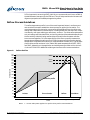
CSN33: Micron BGA Manufacturer’s User Guide Introduction Customer Service Note BGA Manufacturer’s User Guide for Micron BGA Parts Introduction This customer service note provides information that will enable customers to easily integrate both leading-edge and legacy Micron® ball grid array (BGA) packages into their manufacturing processes. It is intended as a set of high-level guidelines and a reference manual describing typical package-related and manufacturing process-flow practices. The recommendations and suggestions provided in this customer service note serve as a guideline to help the end user to develop user-specific solutions. It is the responsibility of the end user to optimize the process to obtain the desired results. Because the package landscape changes rapidly and information can become outdated very quickly, refer to the latest product specifications. Contact your sales representative for any additional questions not covered within this guide. An overview of a typical BGA package and its components are shown in Figure 1. Figure 1: Ball Grid Array Package (Dual Die, Wire Bonded) Silicon die Die attach layer or flip chip with solder bumps Wire bond (typically gold) Mold compound PCB substrate Solder ball JEDEC Terminology This document uses JEDEC terminology. JEDEC-based BGA devices in the semiconductor industry are identified by two key attributes: • Maximum package height (profile) • Ball pitch For example: TFBGA = 1.2mm package height and less than 1.0mm ball pitch. Package descriptors F1 through F6 have been added to provide more detailed ball pitch information for devices with a ball pitch of less than 0.8mm. Within the industry, many memory manufacturers continue to use only the “F” descriptor for any ball pitch of 1.0mm or less (see JEDEC JESD30E for additional information). Maximum package height profile and ball pitch codes based on the JEDEC standard are shown in Tables 1 PDF: 09005aef8479301f/Source: 09005aef84792f7e csn33_bga_user_guide.fm - Rev. C 12/14 EN 1 Micron Technology, Inc., reserves the right to change products or specifications without notice. ©2011 Micron Technology, Inc. All rights reserved. Products and specifications discussed herein are for evaluation and reference purposes only and are subject to change by Micron without notice. Products are only warranted by Micron to meet Micron’s production data sheet specifications. All information discussed herein is provided on an “as is” basis, without warranties of any kind. CSN33: Micron BGA Manufacturer’s User Guide BGA Coplanarity and Warpage Measurement Guidelines and 2. Table 1: Table 2: Ball Pitch Dimensions and Code [JESD30E] Code Name Dimension E Blank F Enlarged Standard Fine F1 Fine F2 Fine F3 Fine F4 Fine F5 Fine F6 Fine 1.50mm 1.00mm and 1.50mm <1.00mm = 0.80mm = 0.75mm = 0.65mm = 0.50mm = 0.40mm = 0.30mm BGA Maximum Package Height Profile [JESD30E] Code Subcode Profile Description Profile Height – – B Blank L T V W U X – – – – B2 B1 – – – – – – – – X1 X2 X3 X4 Extra thick Very thick Thick Standard Low Thin Very thin Very, very thin Ultra thin Extremely thin Extra-thin Super-thin Paper-thin Die-thin 3.50mm >2.45mm and 3.50mm >2.45mm >1.70mm and 2.45mm >1.20mm and 1.70mm >1.00mm and 1.20mm >0.80mm and 1.00mm >0.65mm and 0.80mm >0.50mm and 0.65mm 0.50mm >0.40mm and 0.50mm >0.30mm and 0.40mm >0.25mm and 0.30mm 0.25mm BGA Coplanarity and Warpage Measurement Guidelines Coplanarity is the measure of deviation of the terminals (solder balls) from the seating plane. Refer to JEDEC standard 22-B108B for more definitions and coplanarity measurement methods. Micron BGAs meet the coplanarity specifications documented in the package outline drawings provided in Micron component data sheets as follows: • 100µm for 1.0/0.80/0.65mm ball pitch packages (0.35–0.40mm ball diameter) • 80µm for 0.50mm ball pitch packages (0.3, 0.25, and 0.20mm ball diameter) • This meets the standards described in JEDEC Design Guide 4.5 As part of the manufacturing process, Micron measures coplanarity at room temperature on all BGA packages before shipment to the customer. Warpage is the deformation and deviation from a package’s initial flat surface that occurs during reflow. Package warpage during board assembly can cause the package terminals (solder balls) to have open or short circuit connections after reflow soldering. Warpage is largely driven by the coefficient of thermal expansion (CTE) mismatch between the constituent materials of the BGA package and can also be affected by mois- PDF: 09005aef8479301f/Source: 09005aef84792f7e csn33_bga_user_guide.fm - Rev. C 12/14 EN 2 Micron Technology, Inc., reserves the right to change products or specifications without notice. ©2011 Micron Technology, Inc. All rights reserved. CSN33: Micron BGA Manufacturer’s User Guide Moisture Sensitivity ture absorption. The warpage signature can be either concave (-) or convex (+) (see Figure 2). Refer to JESD22-B112A or JEITA ED 7036 standards for more information and warpage measurement methods. Warpage requirements vary depending on the applications and package dimensions. Micron’s BGA products meet a variety of customer requirements and industry standards. Some BGA products (for example, package-on-package [PoP]) require tighter warpage control than others across the reflow temperature range. Refer to Micron customer service note CSN 34, PoP User Guide, for additional information on PoPs and warpage. Figure 2: Package Warpage Convention [JEITA ED-7036] Concave Convex A Reference plane A B Reference plane Measuring zone B Measuring zone Moisture Sensitivity Plastic IC packages absorb moisture when exposed to atmospheric conditions. During surface mount reflow, absorbed moisture can vaporize and damage the package if not properly controlled. To prevent damage to the package from internal stresses generated by the moisture vaporization process, it is critical that strict adherence to floor life exposure times be followed. The allowable floor life exposure time for any given part is identified on the label for each moisture barrier bag of components contained in the shipment. If the floor life exposure time is exceeded, the components need to be baked dry before surface mount. Refer to Micron’s technical note TN-00-01 and IPC/JEDEC standard J-STD-033B.1 for recommended bake-out conditions. PDF: 09005aef8479301f/Source: 09005aef84792f7e csn33_bga_user_guide.fm - Rev. C 12/14 EN 3 Micron Technology, Inc., reserves the right to change products or specifications without notice. ©2011 Micron Technology, Inc. All rights reserved. CSN33: Micron BGA Manufacturer’s User Guide Surface Mount Design, Materials, and Process Recommendations Surface Mount Design, Materials, and Process Recommendations BGA surface mount assembly typically follows the flow as shown in the Figure 3. Some of the guidelines at each step are provided and the significant factors affecting the yield through surface mount are also briefly discussed in this customer service note. Figure 3: BGA Surface Mount Technology (SMT) Process Flow PCB Design Solder Stencil Design Solder printing and inspection process Device placement Solder reflow Cleaning (optional with no-clean paste) Test/ inspection Pass Fail Rework (if needed) Printed Circuit Board Design Guidelines PCB design guidelines depend on many variables, including ball pitch, ball diameter, and PCB metal land pad type. Solder mask defined (SMD) pads have a solder mask that partially overlaps each metal land pad and defines the pad diameter. Non solder mask defined (NSMD) pads have a solder mask clearance area away from the metal land pads so that each metal land pad diameter is defined by the edges of the metal. Figure 4 and Figure 5 illustrate the difference between SMD and NSMD pads. With SMD pads, the solder flow is restricted to the top of the metallization, which prevents the solder from wetting the sides/wall of the pad as in the case of NSMD. Some of the advantages and disadvantages of the SMD and NSMD are listed below. Application should determine selection of pad type. • For NSMD, definition and control of size and location is easier than SMD (Cu etching has tighter control over the solder masking process) • NSMD pads are smaller and offer more space for trace routing than SMD pads • For fine pitch applications with NSMD, there is increased risk of bridging and so maintaining the solder mask webbing becomes difficult • SMD pads have larger surface area attachment to the laminate, which can prevent pad cratering • SMD solder joints have higher standoff, which makes the joints more robust during shock or drop events • Use of underfill may effect the choice between SMD and NSMD pads depending on application Micron recommends PCB land pad designs maintain a 1:1.2 to 1:1 ratio size between the PCB land pad and the package land pad. Refer to IPC publication 7351B (PCB Design PDF: 09005aef8479301f/Source: 09005aef84792f7e csn33_bga_user_guide.fm - Rev. C 12/14 EN 4 Micron Technology, Inc., reserves the right to change products or specifications without notice. ©2011 Micron Technology, Inc. All rights reserved. CSN33: Micron BGA Manufacturer’s User Guide Stencil Guidelines Guidelines) for additional details regarding metal land pad dimensions and other PCB design considerations. Additional board design factors to consider for maintaining high SMT yields are: • Land pads need to be planar and clean from any foreign materials • Solderability performance (finish shall meet ANSI/J-STD-003 solderability requirements) • Proper selection of pad surface finish materials Figure 4: NSMD and SMD PCB Land Pad Layouts NSMD SMD Copper Pad Copper Pad Diameter of metal land pad Solder mask away from pad Figure 5: Solder mask on pad BGA Solder Ball Attach in NSMD and SMD Pads NSMD SMD Stencil Guidelines As a general design guide, the aperture size should have a 1:1 ratio to the board land size. For BGA applications, a stencil with round or square apertures is recommended. To improve paste release, a positive taper (5° angle) with a bottom opening larger than the top can be used. To achieve good BGA print characteristics, maintain a diameter-tostencil thickness ratio of at least 3:1 (larger openings provide better print quality). Stencil design should follow the IPC stencil guideline IPC7525B as shown in Table 3 on page 6. PDF: 09005aef8479301f/Source: 09005aef84792f7e csn33_bga_user_guide.fm - Rev. C 12/14 EN 5 Micron Technology, Inc., reserves the right to change products or specifications without notice. ©2011 Micron Technology, Inc. All rights reserved. CSN33: Micron BGA Manufacturer’s User Guide Solder Paste and Stencil Printing Guidelines Table 3: General Aperture Design Guideline for BGA (from IPC 7525B Standard) Pitch Land Footprint Dimension BGA Fine pitch BGA 1.25 1.00 Circle, 0.55 Circle, 0.45 Fine pitch BGA 0.50 Circle, 0.25 Fine pitch BGA 0.40 Circle, 0.20 Part Type Aperture Dimension Circle, 0.52mm Square over print 0.42mm Square over print 0.28mm Square over print 0.23mm Stencil Thickness Range Area Ratio Range Solder Paste 0.15–0.20mm 0.115–0.135mm 0.65–0.86 0.65–0.76 Type 3 Type 3 0.075–0.125mm 0.56–0.93 Type 3 0.075–0.100mm 0.56–0.75 Type 3 Solder Paste and Stencil Printing Guidelines The quality of the solder paste is an important factor in producing high-yield assemblies. Water soluble or no-clean paste can be used for the surface mount assembly. Some of the important paste properties are alloy composition, melting point of the alloy, solder powder type/size, clean/no-clean flux, flux activity, rheology, and solder paste shelf/stencil life. Solder paste should be stored at the manufacturer’s recommended temperature and used before the expiration date. The solder paste types, their typical solder powder size, and their classifications are shown in the Table 4. Proper selection of solder paste should be made depending on the application and BGA pitch. Micron has had good surface mount results using Type 3, low residue or no-clean paste meeting the ROL 0 per J-STD-004. Table 4: Solder Paste Types and Particle Size Paste Type Mesh Size (lines-per-inch) Particle Size (µm) Type 2 Type 3 Type 4 Type 5 Type 6 –200/+352 –325/+500 –400/+635 –500 –635 75–45 45–25 38–20 25–25 15–5 To ensure good contact between the solder ball and the PCB pad, optimum solder paste volume is required in the printing step. Some of the important parameters at the printing steps are squeegee speed, force, snap-off, and so on. A stencil with different thicknesses in specific areas, either the top or bottom side(s), can be used to control the paste deposits on PCBs having both standard pitch and fine pitch components. A stepup stencil is one with an area higher and thicker than most of the stencil, and step-down stencils have areas that are lower and thinner than most of the stencil. Some of the factors to consider during solder paste printing are listed below. • Precise volume of solder paste • Stencil alignment and accuracy • Proper stencil cleaning for clogged apertures Device Pick-and-Place Guidelines As the component ball pitch decreases, accurate component placement becomes more important. There are many suppliers for pick-and-place equipment depending on the manufacturing requirements, parts, speed, and so on. Component placement with the PDF: 09005aef8479301f/Source: 09005aef84792f7e csn33_bga_user_guide.fm - Rev. C 12/14 EN 6 Micron Technology, Inc., reserves the right to change products or specifications without notice. ©2011 Micron Technology, Inc. All rights reserved. CSN33: Micron BGA Manufacturer’s User Guide Reflow Process Guidelines PCB is important to ensure high SMT yield. Micron recommends a minimum of 80% of the ball diameter intersect with the PCB land. This will help maximize the inherent selfalignment properties of the BGA package during reflow. Reflow Process Guidelines The reflow temperature profile is one of the most important factors in surface mount and must be fine tuned to establish a robust process for solder joint formation. The actual temperature of the board or components will be different from the reflow oven setting and is dependent on several factors, including board size, thermal mass, component density, oven type, solder type, reflow oven, and so on. The other reflow parameters such as heating ramp rate, dwell time, and cooling rate should be selected depending on the flux activity/chemistry being used and should closely follow the paste manufacturer’s recommendations. It is the responsibility of the user to properly measure the temperature at different locations on the PCB and components to ensure the desired temperature is reached at all locations for complete reflow of solder joint. Typical examples of reflow profile are shown in the Table 6 with peak temperatures of 260°C, 235°C, and 220°C, depending on the application and solder paste type. Refer to Micron’s technical note TN-00-15 for additional soldering and surface mount recommendations. Figure 6: Reflow Profiles Temperature 270 260 250 240 230 220 210 200 260°C 235°C 220°C 180 160 Stepped profile 140 120 Umbrella profile 100 80 60 40 20 Preheat Flux activation Reflow Cooldown 0 Time Notes: PDF: 09005aef8479301f/Source: 09005aef84792f7e csn33_bga_user_guide.fm - Rev. C 12/14 EN MAX time approximately 9 minutes 1. Contact solder paste suppliers for specific reflow profile recommendations. 7 Micron Technology, Inc., reserves the right to change products or specifications without notice. ©2011 Micron Technology, Inc. All rights reserved. CSN33: Micron BGA Manufacturer’s User Guide PCB Cleaning Figure 7: BGA Ball Attribute Before and After Reflow Before Reflow After Reflow Weight of package Package substrate Solder Solder paste Solder mask PCB PCB Cleaning After the surface mount process, some flux residues can be found on the PCB and around the solder joint, which may damage the PCB or package if not cleaned. If a noclean solder paste was used in surface mount, the flux residues don’t have to be cleaned after the soldering process. For tighter pitch and low standoff BGA packages, no-clean solder paste is generally recommended because of the difficulty a cleaning solution would have reaching the underside of the package. If a solder flux used during surface mount requires cleaning, the choice of cleaning process and cleaning solution depend on the package, PCB, and flux (Rosin/aqueous-based) used in the solder paste. Contact the solder paste suppliers for PCB cleaning recommendations. Micron also recommends completely drying the PCB after the cleaning process to remove any residual solvents. If no-clean solder pastes are used during rework or manual soldering operations, the remaining non-activated flux can cause corrosion and the PCB should be carefully inspected. Test and Inspection Some of the common defects encountered with BGA in the SMT assembly process are listed below. • Head-in-pillow: Poor wetting between the solder paste and solder balls. • Solder voids: Voids are cavities or air pockets formed in solder joints that seriously affects the reliability. Voiding can be caused by poor selection of materials, processes, and designs. • Pad crater: Crack formation within the laminate below the solder pad due to mechanical stress during in-circuit testing, board depanelization, connector insertion, or other stresses such as shock and vibration. • Tombstoning: Component tilt during reflow producing an open solder joint. • Popcorning: Moisture evaporation that creates high pressure leading to delamination within a plastic package. In the most extreme cases, the pressure may produce crack and release through the body of the package (referred to as out-gassing). Common inspection techniques to identify defects in SMT assembly can be classified as destructive and nondestructive testing. Some of these techniques are listed below. The user is responsible to identify suitable techniques depending on the application. PDF: 09005aef8479301f/Source: 09005aef84792f7e csn33_bga_user_guide.fm - Rev. C 12/14 EN 8 Micron Technology, Inc., reserves the right to change products or specifications without notice. ©2011 Micron Technology, Inc. All rights reserved. CSN33: Micron BGA Manufacturer’s User Guide Rework • Nondestructive: X-ray (low dose), electrical testing, scanning acoustic microscopy, visual or microscopic (such as 10X) inspections • Destructive: Dye and pry, and micro-section Rework Many manufacturers use a single rework station to incorporate multiple rework process steps, such as component removal, site redress, solder paste/flux application, alignment, component placement, and reflow. Characterizing and storing individual component reflow profiles and the advancement of beam-splitting imaging for alignment/ placement has simplified the rework process significantly. One area of concern with rework is thermal separation of adjoining components during the rework process. Some manufacturers have addressed this by designing hot gas nozzles that maintain the keepout zone around the reworked component to thermally isolate adjacent components during the reflow process. Original equipment manufacturer (OEM) requirements differ when it comes to solder paste and flux-only applications during the rework process. For those requiring solder pastes, microstencils and microsqueegees have been developed to correspond with multiple BGA sizes and ball array footprints. The micro stencil is aligned using the same beam-splitting imaging as component placement. Microsqueegees enable simple, uniform solder paste coverage across the microstencil. Some of the recommended instructions for the rework are listed below. • Prior to rework, parts must be free from moisture (as per supplier labels). • Under-board preheating is required. • The same profile must be used for removal and replacement. The number of times a part can be removed and replaced should be kept to a minimum to prevent internal thermal damage to the printed circuit board. While the use of flux-only attachment has been a common practice for BGA packages in component rework, solder paste is recommended for the best BGA package attachment results. Before implementing flux-only attachment, it is important to note that because this process reduces the amount of solder within the solder joint, BGA stand-off is reduced, and solder joint reliability may be compromised. Manufacturers must evaluate flux-only versus solder paste attachment to determine the most suitable process for their specific application. Reballing BGAs is not recommended for production applications. This is primarily due to the various techniques used to remove excess solder from the bottom side of the BGA following removal from the PCB. Excessive heat during the redress process can damage the BGA. However, when properly controlled, reballing can be executed successfully. Special reball fixtures and tools are available to simplify and help control this process. PDF: 09005aef8479301f/Source: 09005aef84792f7e csn33_bga_user_guide.fm - Rev. C 12/14 EN 9 Micron Technology, Inc., reserves the right to change products or specifications without notice. ©2011 Micron Technology, Inc. All rights reserved. CSN33: Micron BGA Manufacturer’s User Guide Storage and Handling of Components and Boards Storage and Handling of Components and Boards All parts, components, and boards should be stored in an oxygen free environment to prevent oxidation. The product manufacturer’s specifications should always be followed. Some of the practices to avoid when handling electronic assemblies are listed below. • Avoid touching or pressing on component leads • Avoid smashing leads—don’t coin stack units • Avoid putting excessive force on any part of the assembly • Avoid introducing foreign material to any part of the assembly BGA components are particularly susceptible to mechanical damage from mishandling. All processes where bending, flexing, impacting, or dropping the BGA, or where stresses could potentially be transferred to a component when loading it into tooling, test fixtures, sockets, cases, packaging for shipment, and so on, should be closely scrutinized and included in routine preventative maintenance checks. Use of ESD-safe trays and moisture barrier bags for storage and shipping is recommended. References 1. 2. 3. 4. 5. 6. 7. 8. 9. 10. 11. PDF: 09005aef8479301f/Source: 09005aef84792f7e csn33_bga_user_guide.fm - Rev. C 12/14 EN JESD30-B, “Descriptive Designation System for Semiconductor-Device Packages” JEDEC/IPC J-STD-020D.01 JESD22-B108A, “Coplanarity Test for Surface-Mount Semiconductor Devices” J-STD-033B.1, Joint IPC/JEDEC Standard for Handling, Packing, Shipping, and use of Moisture/Reflow Sensitive Surface-Mount Devices J-STD-020D.01, Joint IPC/JEDEC Standard for Moisture/Reflow Sensitivity Classification for Nonhermermetic Solid State Surface-Mount Devices IPC - 7526, “Stencil and Misprinted Board Handbook” IPC - 7525B, “Stencil Design Guideline” IPC - 7351, “PCB Design Guidelines” IPC - 7095B, “Design and Assembly Process Implementation for BGAs” JEITA-ED 7306, “Measurement methods of package warpage at elevated temperature and the maximum permissible warpage” Craig Hillman, “Challenges with Package on Package (PoP); part 1 Manufacturability,” DfR Solutions 10 Micron Technology, Inc., reserves the right to change products or specifications without notice. ©2011 Micron Technology, Inc. All rights reserved. CSN33: Micron BGA Manufacturer’s User Guide Revision History Revision History Rev. C . . . . . . . . . . . . . . . . . . . . . . . . . . . . . . . . . . . . . . . . . . . . . . . . . . . . . . . . . . . . . . . . . . . . . . . . . . . . . . . . . . . . . . . . . . . . . .12/14 • Changed “PCB land pad opening and the package land pad/solder mask opening...” to “PCB land pad and the package land pad” Rev. B . . . . . . . . . . . . . . . . . . . . . . . . . . . . . . . . . . . . . . . . . . . . . . . . . . . . . . . . . . . . . . . . . . . . . . . . . . . . . . . . . . . . . . . . . . . . . .11/12 • Updated all sections Rev. A . . . . . . . . . . . . . . . . . . . . . . . . . . . . . . . . . . . . . . . . . . . . . . . . . . . . . . . . . . . . . . . . . . . . . . . . . . . . . . . . . . . . . . . . . . . . . . . 7/11 • Initial release 8000 S. Federal Way, P.O. Box 6, Boise, ID 83707-0006, Tel: 208-368-3900 www.micron.com/productsupport Customer Comment Line: 800-932-4992 Micron and the Micron logo are trademarks of Micron Technology, Inc. All other trademarks are the property of their respective owners. PDF: 09005aef8479301f/Source: 09005aef84792f7e csn33_bga_user_guide.fm - Rev. C 12/14 EN 11 Micron Technology, Inc., reserves the right to change products or specifications without notice. ©2011 Micron Technology, Inc. All rights reserved.