1
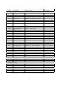
# Signals
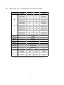
Purpose
I/O standard
4x(16+2)
4x(32+2)
4x(6+1)
32+17
8+7
12
33
4+2
4x(1+1)
4
4
4
2
4x2
4x2
5x1
4
16
DAQ link interface
L1T link interface
SyncData link to PP-FPGA’s
To RO-Tx (POS PHY L3)
ECS
FEM interface
TTCrx interface
Throttle
L1A EvID
Clock 40M Hz distribution
Clock 80M Hz distribution
Clock
Processing mode
L1T processing sync
DAQ processing sync
Initialization done
Resets
GPIO from PP-FPGA’s
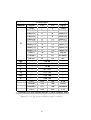
LVTTL
LVTTL
LVTTL
2.5V LVTTL
3.3V LVTTL
3.3VLVTTL
3.3V LVTTL
LVTTL
LVTTL
LVTTL
LVTTL
LVTTL
LVTTL
LVTTL
LVTTL
LVTTL
LVTTL
LVTTL
36
2
3
8x2
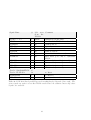
Analyzer interface
ECS I2C
Device address
Termination resister reference
LVTTL
3.3V LVTTL
LVTTL
R
464
Total
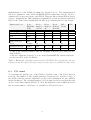
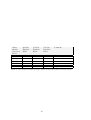
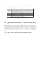
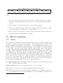
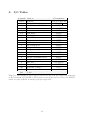
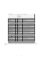
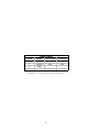
Table 11: The number of I/O’s used for the SyncLink-FPGA with the proposed partitioning of the board of 4 PP-FPGA’s.
32