1
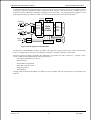
CMS FED-PMC User Manual DRAFT
CMS/FED/PMC/004/2000
CMS Front-End Driver
PMC
User Manual
Version 4.0, Jan 2000
DRAFT VERSION
PMC
CLRC Rutherford Appleton Laboratory
Version 4.0
1
Feb 2000
CMS FED-PMC User Manual DRAFT
CMS/FED/PMC/004/2000
1 Contents
1
CONTENTS . . . . . . . . . . . . . . . . . . . . . . . . . . . . . . . . . . . . . . . . . . . . . . . . . . . . . . . . . . . . . . . . . . . . . . . . . . . . . . . . . . . . . . . . . . . . . . . . . . . . . 2
2
FIGURES. . . . . . . . . . . . . . . . . . . . . . . . . . . . . . . . . . . . . . . . . . . . . . . . . . . . . . . . . . . . . . . . . . . . . . . . . . . . . . . . . . . . . . . . . . . . . . . . . . . . . . . . 4
3
TABLES . . . . . . . . . . . . . . . . . . . . . . . . . . . . . . . . . . . . . . . . . . . . . . . . . . . . . . . . . . . . . . . . . . . . . . . . . . . . . . . . . . . . . . . . . . . . . . . . . . . . . . . . . 4
4
FOREWORD . . . . . . . . . . . . . . . . . . . . . . . . . . . . . . . . . . . . . . . . . . . . . . . . . . . . . . . . . . . . . . . . . . . . . . . . . . . . . . . . . . . . . . . . . . . . . . . . . . . . 5
5
CONTACTS & ORDERING INFORMATION. . . . . . . . . . . . . . . . . . . . . . . . . . . . . . . . . . . . . . . . . . . . . . . . . . . . . . . . . . . . . 5
6
GETTING STARTED. . . . . . . . . . . . . . . . . . . . . . . . . . . . . . . . . . . . . . . . . . . . . . . . . . . . . . . . . . . . . . . . . . . . . . . . . . . . . . . . . . . . . . . . . . 6
6.1
6.2
7
INSTALLATION & JUMPER SETTINGS ................................................................................................. 6
CARRIER CONFIGURATIONS............................................................................................................. 7
INTRODUCTION. . . . . . . . . . . . . . . . . . . . . . . . . . . . . . . . . . . . . . . . . . . . . . . . . . . . . . . . . . . . . . . . . . . . . . . . . . . . . . . . . . . . . . . . . . . . . . . 8
7.1
7.2
8
GENERAL DESCRIPTION .................................................................................................................. 8
ARCHITECTURE ............................................................................................................................. 8
FED-PMC HARDWARE . . . . . . . . . . . . . . . . . . . . . . . . . . . . . . . . . . . . . . . . . . . . . . . . . . . . . . . . . . . . . . . . . . . . . . . . . . . . . . . . . . . . . 1 0
8.1
8.2
8.3
8.4
8.5
8.6
8.7
8.8
8.9
9
FRONT PANEL LAYOUT .................................................................................................................10
FORM FACTOR .............................................................................................................................10
ANALOGUE INPUTS .......................................................................................................................10
CLOCK & TRIGGER FRONT PANEL INPUTS.........................................................................................11
ADC..........................................................................................................................................11
PCI ...........................................................................................................................................11
FPGA........................................................................................................................................11
JUMPERS & SWITCHES...................................................................................................................11
LEDS .........................................................................................................................................12
FED-PMC FUNCTIONALITY . . . . . . . . . . . . . . . . . . . . . . . . . . . . . . . . . . . . . . . . . . . . . . . . . . . . . . . . . . . . . . . . . . . . . . . . . . . . . . 1 3
9.1
9.2
9.3
9.4
9.5
9.6
9.7
9.8
9.9
10
MEMORY REQUIREMENTS ..............................................................................................................13
ADC..........................................................................................................................................13
TRIGGER.....................................................................................................................................13
CLOCK .......................................................................................................................................14
COUNTERS ..................................................................................................................................14
TRIGGER THROTTLE......................................................................................................................14
TEST MODE.................................................................................................................................14
READOUT ...................................................................................................................................15
FIRMWARE..................................................................................................................................15
FED-PMC SOFTWARE . . . . . . . . . . . . . . . . . . . . . . . . . . . . . . . . . . . . . . . . . . . . . . . . . . . . . . . . . . . . . . . . . . . . . . . . . . . . . . . . . . . 1 7
10.1
SOURCE FILES .............................................................................................................................18
10.2
USER LEVEL ROUTINES API ...........................................................................................................18
10.3
PCI CONFIGURATION AND ADDRESS MAP.........................................................................................18
10.3.1
PCI Configuration .................................................................................................................20
10.3.2
Initialisation.........................................................................................................................21
10.3.3
Readout ...............................................................................................................................22
10.3.4
Miscellaneous.......................................................................................................................24
11
EXAMPLE PSEUDO-CODE . . . . . . . . . . . . . . . . . . . . . . . . . . . . . . . . . . . . . . . . . . . . . . . . . . . . . . . . . . . . . . . . . . . . . . . . . . . . . . 2 6
12
EXAMPLES OF USING CARRIERS . . . . . . . . . . . . . . . . . . . . . . . . . . . . . . . . . . . . . . . . . . . . . . . . . . . . . . . . . . . . . . . . . . . 2 9
Version 4.0
2
Feb 2000
CMS FED-PMC User Manual DRAFT
12.1
12.2
12.3
13
CMS/FED/PMC/004/2000
CES RIO2/RTPC RUNNING LYNXOS..............................................................................................29
MOTOROLA MVME2600 SERIES RUNNING LYNXOS...........................................................................29
CARRIERS USING UNIVERSE VME-PCI BRIDGE...................................................................................30
HARDWARE LEVEL DESCRIPTION . . . . . . . . . . . . . . . . . . . . . . . . . . . . . . . . . . . . . . . . . . . . . . . . . . . . . . . . . . . . . . . . . . 3 1
13.1
DIGITAL .....................................................................................................................................31
13.1.1
Dual-Port Memory.................................................................................................................31
13.1.2
PCI Bridge ...........................................................................................................................31
13.1.2.1
13.1.2.2
13.1.3
PCI Configuration Registers ...............................................................................................3 1
Local Configuration Registers .............................................................................................3 2
CPLD .................................................................................................................................32
13.1.3.1
13.1.3.2
13.1.4
Configuration Sequencing ..................................................................................................3 2
Serial Configuration Interface..............................................................................................3 2
FPGA .................................................................................................................................35
13.1.4.1
13.1.4.2
13.1.4.3
13.1.4.4
13.1.4.5
i960 Interface..................................................................................................................3 5
DPRAM Interface .............................................................................................................3 5
Registers .......................................................................................................................3 5
Trigger and Buffer Management............................................................................................3 8
Event Counters and Event FIFO ............................................................................................3 8
13.2
CPLD CONFIGURATION.................................................................................................................39
13.2.1
Lattice download cable............................................................................................................39
13.3
FPGA READ-BACK.......................................................................................................................39
13.4
BOARD SET-UP.............................................................................................................................39
13.4.1
PCI 9080 configuration ..........................................................................................................39
13.4.2
FPGA Configuration..............................................................................................................39
13.4.2.1
13.4.2.2
PCI space .......................................................................................................................3 9
Flash EEPROM ................................................................................................................3 9
13.5
BOARD OPERATION.......................................................................................................................40
13.5.1
Boot-up ...............................................................................................................................40
13.5.2
Runtime ..............................................................................................................................40
14
APV HEADER FINDING MODE . . . . . . . . . . . . . . . . . . . . . . . . . . . . . . . . . . . . . . . . . . . . . . . . . . . . . . . . . . . . . . . . . . . . . . . . 4 0
15
DEBUGGING TOOLS. . . . . . . . . . . . . . . . . . . . . . . . . . . . . . . . . . . . . . . . . . . . . . . . . . . . . . . . . . . . . . . . . . . . . . . . . . . . . . . . . . . . . . 4 1
16
WEB SERVER . . . . . . . . . . . . . . . . . . . . . . . . . . . . . . . . . . . . . . . . . . . . . . . . . . . . . . . . . . . . . . . . . . . . . . . . . . . . . . . . . . . . . . . . . . . . . . 4 1
17
TROUBLE SHOOTING . . . . . . . . . . . . . . . . . . . . . . . . . . . . . . . . . . . . . . . . . . . . . . . . . . . . . . . . . . . . . . . . . . . . . . . . . . . . . . . . . . . . 4 1
17.1
17.2
17.3
17.4
17.5
17.6
17.7
17.8
17.9
17.10
LED DOES NOT COME ON AT POWER ON? ..........................................................................................41
FED HANGS AFTER ENABLING EXTERNAL CLOCK ? ..............................................................................41
EVENT & BUNCH CROSSING COUNTERS DON’T RESET FOR A NEW RUN? ....................................................41
BUFFER OVERFLOWS OR NUMBER OF FILLED BUFFERS IS NOT AS EXPECTED?...............................................42
NO SOFTWARE TRIGGERS? ..............................................................................................................42
SAME EVENT IS READOUT MORE THAN ONCE? ....................................................................................42
NO HARDWARE TRIGGERS? .............................................................................................................42
THE DPM IS FULL OF VALUES LIKE 256,257 OR 0?..............................................................................42
THE EVENT COUNTER DOUBLE COUNTS?............................................................................................42
SPURIOUS TRIGGERS RECEIVED?...................................................................................................43
18
APPENDIX A: FED-PMC MK1. . . . . . . . . . . . . . . . . . . . . . . . . . . . . . . . . . . . . . . . . . . . . . . . . . . . . . . . . . . . . . . . . . . . . . . . . . 4 4
19
APPENDIX B: CERN TEST BEAM SETUP . . . . . . . . . . . . . . . . . . . . . . . . . . . . . . . . . . . . . . . . . . . . . . . . . . . . . . . . . . . 4 4
20
APPENDIX C: PMC J4 AUX CONNECTOR. . . . . . . . . . . . . . . . . . . . . . . . . . . . . . . . . . . . . . . . . . . . . . . . . . . . . . . . . . 4 5
21
REFERENCES . . . . . . . . . . . . . . . . . . . . . . . . . . . . . . . . . . . . . . . . . . . . . . . . . . . . . . . . . . . . . . . . . . . . . . . . . . . . . . . . . . . . . . . . . . . . . . 4 7
Version 4.0
3
Feb 2000
CMS FED-PMC User Manual DRAFT
CMS/FED/PMC/004/2000
2 Figures
FIGURE 1 JUMPERS PL10 & PL11.................................................................................................................... 6
FIGURE 2 PHOTOGRAPH SHOWING BOTH SIDES OF THE FED-PMC (MK2) ................................................................ 8
FIGURE 3 BLOCK DIAGRAM OF THE FED-PMC ................................................................................................... 9
FIGURE 4 FED-PMC FRONT PANEL LAYOUT ...................................................................................................10
FIGURE 5 EVENT FORMAT IN DPM .................................................................................................................16
FIGURE 6 LAYERED SOFTWARE DESIGN ...........................................................................................................17
FIGURE 7 FED ADDRESS MAP (AS SET UP BY USER LIBRARY ROUTINES)...................................................................19
3 Tables
TABLE 1 EXAMPLE JUMPER SETTINGS FOR VME PMC CARRIERS ............................................................................ 6
TABLE 2 CLOCK DELAY SETTINGS ...................................................................................................................14
TABLE 3 READOUT SAMPLE SIZES....................................................................................................................15
TABLE 4 PCI BRIDGE CONFIGURATION REGISTERS .............................................................................................31
TABLE 5 LOCAL BRIDGE CONFIGURATION REGISTERS..........................................................................................32
TABLE 6 SERIAL CONFIGURATION COMMANDS ..................................................................................................33
TABLE 7 SERIAL CONFIGURATION REGISTERS ....................................................................................................33
TABLE 8 CLOCK DELAY SETTINGS ...................................................................................................................34
TABLE 9 CLOCK SOURCE SELECTION................................................................................................................34
TABLE 10 SERIAL SUB-COMMANDS ..................................................................................................................34
TABLE 11 SERIAL STATUS REGISTER ................................................................................................................34
TABLE 12 DPM ADDRESS MAP........................................................................................................................35
TABLE 13 FED REGISTER MAP........................................................................................................................36
TABLE 14 FIFO CONTENTS ............................................................................................................................38
Version 4.0
4
Feb 2000
CMS FED-PMC User Manual DRAFT
CMS/FED/PMC/004/2000
4 Foreword
This document is intended for the general user of the CMS Front-End Driver PMC.
It should contain sufficient information to install and operate the FED-PMC Mk2 (and Mk11) cards.
This document together with additional FED-PMC documentation and software can be obtained from t h e
following web site:
http://hepwww.rl.ac.uk/cms_fed/default.htm
Please send any comments on the contents of this document to the editor [email protected]
Please Note: This is a working document and is subject to revision.
5 Contacts & Ordering Information
Further information concerning the FED-PMC can be obtained from the following web site:
http://hepwww.rl.ac.uk/cms_fed/default.htm
All queries concerning the operation of the FED-PMC and its associated software should be addressed to:
Dr John Coughlan
CLRC Rutherford Appleton Laboratory
Chilton
Didcot
Oxfordshire
OX11 0QX
UK
email : J.Coughlan@ rl.ac.uk
Orders for FED-PMCÕs from the CMS Tracker community should be addressed to Prof. Geoff Hall a t
Imperial College, London (contact : [email protected]).
All other orders should be addressed to the RAL Instrumentation group (contact : [email protected]).
1
The Mk1 version of the PMC is described in Appendix A: FED-PMC Mk1.
Version 4.0
5
Feb 2000
CMS FED-PMC User Manual DRAFT
CMS/FED/PMC/004/2000
6 Getting Started
The FED-PMC is delivered in a box/plastic bag with protection from electrostatic discharge.
It is recommended to observe ESD protections when handling the FED-PMC and associated carrier boards.
The reference number printed on the card is PC3109M/1 & PC3109M/2 for Mk1 & Mk2 cards respectively.
A label showing the serial number should also be clearly visible.
Sufficient LEMO connectors for all front panel inputs are supplied with each card.
6.1
Installation & Jumper Settings
The FED-PMC Mk2 is capable of being plugged on to all standard VME PMC carrier boards.
Before placing the PMC on the carrier please check the following 2 static options:
1. Jumper PL1 (the single jumper)
If the VME carrier does NOT supply 3.3 V this jumper should be OFF in order to enable the onboard
supply.
2. Jumpers PL10 & Pl11
If the VME carrier does NOT supply VCCIO both jumpers should be ON ( jumpers should be placed
VERTICALLY) (see Figure 1)
Figure 1 Jumpers PL10 & PL11
NB If your FED-PMC does NOT have these 3 jumpers then you have a Mk1 card (see Appendix A).
VME Carrier
Mk1 Usable
Jumper PL1
Jumpers PL10 & PL11
CES RIO2/RTPC
YES
ON
ON
Motorola MVME2600
YES
ON
ON
VMETRO MIDAS-20
NO
OFF
ON
Interphase 6200
NO
OFF
ON
ESD Caddy
YES
ON
ON
Table 1 Example Jumper settings for VME PMC carriers
Version 4.0
6
Feb 2000
CMS FED-PMC User Manual DRAFT
CMS/FED/PMC/004/2000
Table 1 shows some standard carrier configurations. For other cases please refer to the documentation
provided with your carrier.
The PMC is delivered with all 3 jumpers on.
The PMC has one indicator red LED (location top right of visible side of PMC when mounted).
On power up the LED should come ON. If the LED fails to come on it is likely the PMC is not receiving t h e
3.3 V supply. (NB after the FPGA is loaded the LED goes OFF).
6.2
Carrier Configurations
The FED-PMC is capable of being used on all standard VME PMC carrier boards.
At the time of writing it has been operated with the following Carrier/OS configurations:
CES RIO2/RTPC
Motorola MVME2600 series
VMETRO MIDAS-202
Interphase 62003
ESD Caddy
PowerPC SBC running LynxOS or VxWorks.
PowerPC SBC running LynxOS
Dumb Carrier
Dumb Carrier
Dumb Carrier
Refer to section 12 for examples of how to use these carriers with the FED-PMC.
2
3
MIDAS-20 does not supply 3.3 V
Interphase 6200 does not supply 3.3 V
Version 4.0
7
Feb 2000
CMS FED-PMC User Manual DRAFT
CMS/FED/PMC/004/2000
7 Introduction
7.1
General Description
The FED-PMC is an 8 channel ADC on a (32 bit at 33 MHz) PCI Mezzanine Card [1]. It represents the next
generation FED following the earlier 9U VME prototype board [2]. It incorporates on board data transfer
and buffering circuitry and outputs data over PCI bus. The Mk2 version of the card is described in this
document.
Figure 2 Photograph showing both sides of the FED-PMC (Mk2)
The choice of the PMC format, which interfaces via the popular PCI bus, allows the FED prototype to be
used on a wide variety of commercial off-the-shelf VME carrier boards. The FED-PMC is thus intended
to provide a cost effective solution to the prototyping requirements of the Tracker community. The FEDPMC ÒpackageÓ also includes all the necessary software for FED set-up and readout.
7.2
Architecture
A diagram indicating the basic functional units of the FED-PMC is shown in Figure 3. The card has 8
electrical input channels which can be configured at assembly for either differential or single-ended
inputs. Each channel utilises a commercial ADC and is capable of digitising 9 bits4 at clock speeds from
between 2 and 40 MHz.
The data is stored in contiguous blocks inside a Dual Ported Memory (DPM). The DPM is implemented as
4 x 64K x 18 bit synchronous memories and is capable of buffering the raw data from approximately 250
APV frames. The data is read out (can be done in parallel with ADC capture) over the PCI bus via a 32
bit, 33 MHz commercial bridge interface. A FIFO provides storage for event buffer pointers and event
counter information.
4
ADC’s are 10 bit devices, LSB is not readout
Version 4.0
8
Feb 2000
CMS FED-PMC User Manual DRAFT
CMS/FED/PMC/004/2000
A CPLD implements the clock and trigger control. Trigger and clock (LVDS) signals are brought in on t h e
front panel. The fine adjustment of the clock phase with respect to the data can be set under software
control in order to obtain the optimum sampling point at the ADC. For testing purposes triggers can be
generated internally by software and the card can run from the internal PCI clock (33 MHz).
address
FIFO
Channel 0
+
Net
op-amp
ADC
Dual
Ported
Memory
screen
Channel 7
+
Net
~
~
~
~
op-amp
FPGA
Xilinx
XC 4036
PCI
interface
PLX
9080
J1
J2
ADC
screen
TTC interface
address
Trigger +
LVDS
receiver
Clock +
LVDS
receiver
Trigger
CPLD
Phase Control
LVDS
receiver
J4
Clock
Figure 3 Block diagram of the FED-PMC
At the heart of the FED-PMC design is an FPGA. This permits a large fraction of the cardÕs functionality
to be re-configurable in firmware and thereby maintains a flexible hardware architecture.
The basic firmware design configures the FED-PMC to provide raw data capture in a Òdigital scopeÓ
mode. VHDL blocks implement the following functions:
- Local data and address bus (slave)
- DPM interface
- Event buffer management
- FIFO and counters control
- Register interface
- Test functions
During normal operation the FPGA is loaded on power up under software control from an on-board Flash
memory.
Version 4.0
9
Feb 2000
CMS FED-PMC User Manual DRAFT
CMS/FED/PMC/004/2000
8 FED-PMC Hardware
8.1
Front Panel Layout
The arrangement of the analogue and trigger/clock inputs (with polarities) is shown in Figure 4.
TOP
AnalogueInput #7
1
2
AnalogueInput #6
AnalogueInput #5
1 Inverting input
2 Non inverting input
AnalogueInput #4
Clock& Trigger Input
4
3
1
2
AnalogueInput #3
AnalogueInput #2
1 CLK_FP+
2 CLK_FP3 TRIG_FP 4 TRIG_FP +
AnalogueInput #1
AnalogueInput #0
Figure 4 FED-PMC Front Panel Layout
8.2
Form Factor
Single PMC
8.3
75 x 150 mm
Analogue Inputs
The Analogue Inputs can be configured as either differential or single ended at assembly.
NB By default all cards are delivered with the same configuration as those used in the CMS Tracker test
beam in April 1999 i.e. Differential inputs ±0.75V with an internal amplifier gain of 2 (to match full
ADC range 0-3V).
(Alternative assembly instructions can be implemented on request.)
Version 4.0
10
Feb 2000
CMS FED-PMC User Manual DRAFT
CMS/FED/PMC/004/2000
Number
8
Connector type
LEMO part no. FGG.00.302.CLAD35 (supplied with PMC delivery)
Differential range ±0.75V max
Single Ended Range±0.75V typ ± 1.50 V max5
Termination
8.4
100Ω
50Ω
differential
single ended
stp
co-ax
Clock & Trigger Front Panel Inputs
Connectors LEMO part no. FGG.00.304.CLAD35 (supplied with PMC delivery)
Levels
LVDS [3]
CLK
TRIG
8.5
2MHz to 40MHz
synchronous to CLK
ADC
Device used
Conversion rate
Max Resolution
8.6
SPT 7861 [4]
2MHz - 40MHz continuously sampling
9 Bit (10 Bit Converter - LSB is not used)
PCI
Connector
PMC J1, J2
Clock Speed
<33MHz
Switching regime 5V
Bus width
32 bit
Bridge
PLX PCI 9080 [5]
PCI Specification v 2.1
PCI Configuration Space (64 bytes) standard configuration header
PCI Memory Space 2 MByte occupied as one contiguous block
PCI I/O space
None
The FED-PMC is configured as a PCI Target (i.e. Slave access only).
8.7
FPGA
XILINX XC4036XL [6].
8.8
Jumpers & Switches
See section Installation & Jumper Settings.
5
Single ended input range is controlled by the gain of the input amplifier which is set during assembly.
Version 4.0
11
Feb 2000
CMS FED-PMC User Manual DRAFT
8.9
CMS/FED/PMC/004/2000
LEDs
The FED-PMC has a red LED located at the top right of the side without connectors (i.e. the side still
visible when plugged on the carrier). The LED should go ON when the card is powered up. It should go
OFF after the FPGA has been loaded.
Version 4.0
12
Feb 2000
CMS FED-PMC User Manual DRAFT
CMS/FED/PMC/004/2000
9 FED-PMC Functionality
The use of FPGA devices means that the FED-PMC functionality is re-configurable in firmware.
This section describes the functionality of the FED-PMC with the following FPGA firmware:
Version
0
Revision
2
(This is the so called ÒScope modeÓ)
In order to guard the user from future modifications in the firmware, the provided library of C routines
should be used to configure and readout the FED.
9.1
Memory Requirements
The precise arrangement of registers in memory is subject to change.
All access should be made using the software routines provided.
The card has the following PCI space requirements:
PCI Configuration Space
64 bytes
PCI Bridge (see [5] for configuration registers description)
PCI Memory Space
1 MByte
DPM
256 bytes
Registers & FIFO's
256 bytes
PCI Bridge
+ (1 MByte - 512 bytes) reserved.
TOTAL = 2 MBytes
PCI I/O Space
None Used
9.2
ADC
The 8 ADC channels are grouped into 4 pairs. The outputs of each pair can be enabled or disabled.
Normally ALL channels should be enabled.
9.3
Trigger
There are 2 possible Trigger sources (section ):
External Front Panel LVDS (Trigger pulse width = 25 nsec)
Software (only available in ÒTest ModeÓ)
After a PCI reset external triggers are ENABLED.
The only Trigger mode presently implemented is ÒStart DigitisationÓ.
In this mode a trigger pulse (either external or software) during a digitisation run causes a pre-set number
of samples to be digitised and stored in the DPM.
Version 4.0
13
Feb 2000
CMS FED-PMC User Manual DRAFT
CMS/FED/PMC/004/2000
IMPORTANT: If N further triggers arrive during the data capture period from the first trigger the data
from these N later trigger will be LOST. (What actually happens is that the data from the first trigger
is stored in DPM 1 + N times!)
E.g. If sample size is 512 and clock frequency is 40 MHz then minimum separation of triggers should be
approx. 512x25 nsec ≈ 12.8 µsec
9.4
Clock
There are 2 possible clock sources:
Front Panel LVDS
PCI clock internal (33 MHz)
After reset the internal PCI clock is ENABLED.
NB The selected clock is used to drive all the logic circuits of the FED and must ALWAYS be running (i.e.
if external clock is selected it must never be interrupted)
A delay can be introduced into the clock signal path (in 10 steps of 25 nsec) which allows the phase of t h e
clock relative to the data to be adjusted.
Delay Setting6
1
2
3
4
5
6
7
8
9
10
Delay register (nsec)
2.5
5.0
7.5
10.0
12.5
15.0
17.5
20.0
22.5
25.0
Table 2 Clock delay settings
9.5
Counters
During the digitisation run the following counters are enabled:
Event counter => counts Triggers.
Bunch Crossing counter => counts Clocks (i.e. wraps around).
After a PCI reset the counters are zeroed.
9.6
Trigger Throttle
If the number of occupied buffers exceeds a programmable limit a hardware signal line FAST_WARN
(see Appendix C: PMC J4 Aux Connector) routed via J4 connector can be generated to inhibit further
triggers.
9.7
Test Mode
If Test Mode is enabled triggers can be generated by software (NB external triggers are disabled).
After a PCI reset Test mode is DISABLED.
6
as passed to fedpmc_init() routine.
Version 4.0
14
Feb 2000
CMS FED-PMC User Manual DRAFT
9.8
CMS/FED/PMC/004/2000
Readout
On receipt of a trigger (either external or software) the data from a pre-set number of samples is captured
in the DPM.
IMPORTANT: Only certain sample sizes are permitted (see Table 3). Illegal sample sizes will result in
unpredictable readout values.
Number Samples
Number Bytes
Max Events in DPM
16
256
4K
32
512
2K
64
1K
1K
128
2K
512
256
4K
256
512
8K
128
1K
16K
64
2K
32K
32
4K
64K
16
8K
128K
8
16K
256K
4
32K
512K
2
Table 3 Readout sample sizes
The data from triggers are stored in the DPM in consecutive, contiguous buffers.
Note: The data from the 8 ADC channels of each sample are interleaved. Therefore it is NOT possible to
suppress the readout from individual ADC channels).
The format of an event (with 512 samples) in the DPM is shown in Figure 5.
9.9
Firmware
The contents of the FPGA are stored permanently in a Flash EEPROM.
The version of the firmware stored can be read back by software.
The FED-PMC hardware serial number can also be read back.
Version 4.0
15
Feb 2000
CMS FED-PMC User Manual DRAFT
CMS/FED/PMC/004/2000
Bit#
DPM Address $
31
16
24
8
0
0000
0000000
1
0000000
0
0004
0000000
3
0000000
2
0008
0000000
5
0000000
4
000C 0000000
0010 0000000
7
0000000
6
1
0000000
0
0014
0000000
3
0000000
2
0018
0000000
5
0000000
4
001C 0000000
7
0000000
6
1FF0 0000000
1
0000000
0
1FF4 0000000
3
0000000
2
1FF8 0000000
1FFC 0000000
5
0000000
4
7
0000000
6
........
Sample #
1
2
.
512
Next Event starts at $2000
Figure 5 Event Format in DPM
Version 4.0
16
Feb 2000
CMS FED-PMC User Manual DRAFT
CMS/FED/PMC/004/2000
10 FED-PMC Software
The FPGA-based open hardware architecture is complemented by the design of the software architecture
which forms an integral part of the delivered FED-PMC package. The software design follows a layered
approach from the lowest-level drivers right up to a full graphical user interface.
A layered design (Figure 6) has several advantages for the end user:
- It abstracts the details of the hardware implementation. At the simplest level a handful of routine
calls are required for card configuration and readout operation.
- It removes the need to rewrite code which has already been debugged in parallel with the hardware
- It permits upgrades to the firmware to be transparently implemented. The firmware contains a version
identifier permitting the software to recognise the design currently installed and operate accordingly.
GUI
Future Extensions
Network Layer
Calling Sequence
Network Layer
Entry Level
User
GUI
High-Level VIs
Programmer
Low-Level VIs
C Library
Low-Level C Primitives
Expert
Platform-Dependent Primitives
(BErr, Block Move…)
Front-End Driver PMC
Figure 6 Layered Software Design
The software is implemented by a comprehensive library of (open source) C routines which allow for a l l
aspects of card configuration and readout operation. This allows the FED-PMC to be integrated into a
custom system without first having to understand all the aspects of the hardware. The software assumes
the FED-PMC is memory mapped onto the host processorÕs address space.
A high-level graphical user interface for the FED-PMC, implemented using LabView, has also been
developed for the test bench at RAL.
Version 4.0
17
Feb 2000
CMS FED-PMC User Manual DRAFT
CMS/FED/PMC/004/2000
10.1 Source Files
All the necessary source and header files are available from the web server.
All files are written in ANSI C.
Header files:
fedpmc_defs.h
fedpmc.h
fedpmc_xilinx.h
fedpmc_pci9080.h
fedpmc_carrier.h
routine declarations
register definitions
FPGA definitions
PCI bridge specific definitions
PMC carrier specific definitions
Source files:
fedpmc.c
fedpmc_regs.c
fedpmc_fpga.c
fedpmc_pci9080.c
fedpmc_util.c
fedpmc_carrier.c
high level user routines
low level FED register routines
FPGA specific routines
PCI bridge specific routines
utility routines
PMC carrier specific routines
10.2 User Level Routines API
The routines described in this section should be sufficient for normal user operation of the FED-PMC.
An example of their use in a simple readout system is given in section.
10.3 PCI Configuration and Address Map
The FED-PMC has a wide community of users employing a diverse range of PMC carriers, host processors
and Operating Systems. The User Libraries have therefore been written to be as simple and portable as
possible.
The core routines required to setup and readout the FED are written in ANSI C and do not rely on
processor/OS specific calls or even on the C library functions. Where ANSI C library functions are used
this is clearly indicated.
Access to the FED is via a simple memory map. Drivers have not yet been implemented and no attempt
has been made to use interrupts.
The FED-PMC resources are located in 3 distinct PCI memory spaces (section 13.1.2.1). Before the FED
routines can be used the memory mapping to these spaces has to be set up on the bridge chip of the FEDPMC7.
The routine described in section 10.3.1 used to configure the PCI bridge has been tailored to specific PMC
carriers where necessary. This routine arranges the 3 spaces to be contiguous as shown in Figure 7.
All other routines depend on this memory mapping and are passed a single base address to allow access to
the FED resources.
7
Note that the Mk1 and Mk2 PMC’s are not equipped with a serial EEPROM attached to the PCI bridge. Therefore all the
configuration information, including address space sizes, required by the host must also be explicitly set up. Some
special handling may be necessary for certain BIOS’s.
Version 4.0
18
Feb 2000
CMS FED-PMC User Manual DRAFT
CMS/FED/PMC/004/2000
The address path between the host processor and the FED will also depend on the precise configuration of
the carrier. Hence the configuration routines are carrier dependent.
PCI Address
Local Bus
Address
FED Base = PCIBAR2
$00’0000
FED DPM
(1 MB)
PCIBAR3
(= PCIBAR2 + $10’0000)
PCIBAR0
(= PCIBAR2 + $10’1000)
$10’0000
FED FIFO (128 Bytes)
FED Registers (128 Bytes)
$10’0080
$10’1000
Bridge Local Registers
(256 Bytes)
$10’0200
Reserved
(1 MB - 512 Bytes)
$20’0000
Figure 7 FED Address Map (as set up by User Library routines)
Version 4.0
19
Feb 2000
CMS FED-PMC User Manual DRAFT
10.3.1
CMS/FED/PMC/004/2000
PCI Configuration
The first step is to set the PCI Memory base address registers for the FED. These registers are located in
standard PCI configuration space. FED library routines expect a specific mapping which is set up in t h e
following routine.
fedpmc_config_memory() should continue be used with CES RIO or Motorola PPC carriers.
(For carriers employing the Tundra Universe VME-PCI bridge chip (e.g. MIDAS20) see section N).
long fedpmc_config_memory(
long pci_cfg_base, long abs_pci_mem_base, long carrier, long device_number)
pci_cfg_base:
abs_pci_mem_base:
carrier:
device_number
return_value:
Base address in PCI configuration space for PMC slot (as seen by HOST).
Base address chosen for PCI memory space for FED (ABSOLUTE address!).(1)
Carrier board type:
1 = CES RIO2/RTPC
2 = Motorola PPC MVME2600 series
PCI device number (Carrier & PMC slot dependent):
0
OK.
(1) The corresponding address as seen by HOST = fedpmc_base is passed to all other FED_PMC routines.
IMPORTANT: The USER must ensure this space is not used by any other PCI devices.
Example: CES RIO2/RTPC lower PMC slot:
pci_cfg_base = 0x80802000 (assumes processor has direct h/w access)
abs_pci_mem_base = 0x01000000 (located in unused pci space on RIO2/RTPC)
carrier = 1
device_number = 0 (unused)
This routine initialises the PCI bridge configuration registers.
It sets up the memory mapped base addresses for all subsequent routine calls.
It MUST be the first call after a reset of the card.
NB This is the ONLY routine which accesses PCI configuration space (i.e. all other routines access PCI
memory space only).
long fedpmc_config_bridge(long fedpmc_base)
fedpmc_base:
return_code:
FED base address in PCI memory space (as seen by HOST).
0
OK
This routine completes the configuration of the PCI bridge local bridge registers.
It should be called immediately after fedpmc_config_memory().
Version 4.0
20
Feb 2000
CMS FED-PMC User Manual DRAFT
10.3.2
CMS/FED/PMC/004/2000
Initialisation
long fedpmc_status_fpga(long fedpmc_base)
fedpmc_base:
return_code:
FED base address in PCI memory space (as seen by HOST).
0
FPGA IS already Loaded.
1
FPGA is NOT yet Loaded.
This routine returns the load status of the FPGA.
NB After loading the contents in FPGA are only lost again when power is turned OFF, i.e. they are NOT
lost after a Reset.
void fedpmc_config_fpga(long fedpmc_base)
fedpmc_base:
FED base address in PCI memory space (as seen by HOST).
This routine causes the firmware (permanently stored) in Flash EEPROM to be loaded into the FPGA.
The operation takes about 5 seconds. (The LED should go OFF once FPGA is loaded.)
long
long
long
long
fedpmc_init(long fedpmc_base,
clock_source, long clock_delay, long ext_trigger_source, long trigger_mode,
adc_chan_mask, long adc_sample_freq, long adc_samples,
trigger_throttle_enable, long trigger_throttle_threshold)
fedpmc_base:
clock_source:
FED base address in PCI memory space (as seen by HOST).
0 => PCI internal
2 => Front Panel (1)
clock_delay:
[0..10] (for corresponding delay values see Table 2).
ext_trigger_source: 0 => Front Panel
trigger_mode:
0 => Start Digitisation
adc_chan_mask: [$0..$f]
bit #0 = 1/0 enables / disables ADC pair 0 & 1
bit #1 = 1/0 enables / disables ADC pair 2 & 3
bit #2 = 1/0 enables / disables ADC pair 4 & 5
bit #3 = 1/0 enables / disables ADC pair 6 & 7
adc_sample_freq:
0
No downsampling (sample every clock)
1
Downsample (sample every 2nd clock)8
adc_samples:
[16..32K] = Number of ADC samples to readout per event (2)
trigger_throttle_enable:
0
Throttle signal disabled
1
Throttle signal enab led
trigger_throttle_threshold:
Number of occupied buffers at which throttle signal appears.
return_code:
0
8
11
OK
error invalid number of ADC samples (2)
error canÕt initialise during digitisation run.
(1) NB User must ensure the Front Panel clock is running BEFORE selecting it or FED will hang up.
8
adc_samples parameter should be adjusted accordingly
Version 4.0
21
Feb 2000
CMS FED-PMC User Manual DRAFT
CMS/FED/PMC/004/2000
(2) ONLY certain values are permitted (see Table 3).
This routine should be called to configure the FED PMC registers prior to readout.
It should be called OUTSIDE of digitisation run.
10.3.3
Readout
void fedpmc_reset_counters(long fedpmc_base)
fedpmc_base:
FED base address in PCI memory space (as seen by HOST).
This routine resets the event and bunch crossing counters.
NB It should only be called DURING a digitisation run.
long fedpmc_purge_buffers(long fedpmc_base)
fedpmc_base:
return_value:
FED base address in PCI memory space (as seen by HOST).
Number of buffers that were purged.
This routine clears all pending events in the DPM.
(It does this by flushing the FED FIFO. The buffer occupancy counter is not reset to 0 until the start of t h e
next run).
In order to ensure clean buffer situation it is recommended it be called before each new digitisation run.
(It can also be called during a digitisation run.)
void fedpmc_start_digitisation(long fedpmc_base)
fedpmc_base:
FED base address in PCI memory space (as seen by HOST).
This routine turns the digitisation run ON.
(Note The ADCs run continously. This routine enables the capture of ADC output in the DPM)
void fedpmc_stop_digitisation(long fedpmc_base)
fedpmc_base:
FED base address in PCI memory space (as seen by HOST).
This routine turns the digitisation run OFF.
(Note The ADCs run continously. This routine disables the capture of ADC output in the DPM)
void fedpmc_occupied_buffers(long fedpmc_base,
long* filled_buffers)
fedpmc_base:
filled_buffers:
FED base address in PCI memory space (as seen by HOST).
Returns number of occupied buffers.
This routine returns the number of occupied buffers i.e. number of pending events for readout.
(The buffer occupancy is reset to 0 at the start of each run).
Version 4.0
22
Feb 2000
CMS FED-PMC User Manual DRAFT
CMS/FED/PMC/004/2000
long fedpmc_readout_event(long fedpmc_base,
long* dest, long* size, long* event, long* bunch_crossing,
long* number_samples, long* buffer_address, long format_flag, long dma_flag
long skip_begin, long skip_end)
fedpmc_base:
dest:
size:
event:
bunch_crossing:
number_samples:
buffer_address:
dma_flag:
format_flag:
skip_begin:
skip_end:
return_code:
FED base address in PCI memory space (as seen by HOST).
Destination address for readout data (as seen by HOST)..
Returns total number of bytes readout (including formatting data).
Returns event number counter.
Returns bunch crossing number counter.
Returns number of samples requested for this event.(1)
Returns buffer address in DPM (for debugging purposes).
0 =>DMA is NOT implemented yet.
0 => Formatting is NOT implemented yet.
Number of samples to skip in readout at beginning of data. (2)
Number of samples to skip in readout at end of data.(2)
0
OK
11
No events pending.
22
Event FIFO empty.
33
Error Illegal buffer pointer.
(1) Value should agree with value set in fedpmc_init().
(2) Useful for removing empty samples around APV frame and hence speeding up readout.
This routine reads out the next event in the DPM putting the readout data at address ÒdestÓ.
It can be called inside OR outside a digitisation run.
NB The act of reading out a buffer frees the DPM memory occupied by that event.
Version 4.0
23
Feb 2000
CMS FED-PMC User Manual DRAFT
10.3.4
CMS/FED/PMC/004/2000
Miscellaneous
These routines may be useful for testing FED-PMC status & debugging user code.
long fedpmc_status(long fedpmc_base,
long* clock_source, long* clock_delay, long* ext_trigger_source,
long* trigger_mode, long* adc_chan_mask,
long* adc_sample_freq, long* event_size,
long* trigger_throttle_enable, long* trigger_throttle_threshold)
fedpmc_base:
clock_source:
FED base address in PCI memory space (as seen by HOST).
0 => PCI internal
2 => Front Panel
clock_delay:
[0..10].
ext_trigger_source: 0 => Front Panel
trigger_mode:
0 => Start Digitisation
adc_chan_mask: [$0..$ff] (1)
adc_sample_freq:
0
No downsampling (sample every clock)
1
Downsample (sample every 2nd clock)9
adc_samples:
[16..32K] = Number of ADC samples to readout per event
trigger_throttle_enable:
0
Throttle signal disabled
1
Throttle signal enab led
trigger_throttle_threshold:
Number of occupied buffers at which throttle signal appears.
This routine simply gives the status of the fed settings set-up in fedpmc_init().
(1) adc_chan_mask returns contents of physical register and will NOT agree with value set in
fedpmc_init()
void fedpmc_enable_test_mode(long fedpmc_base)
fedpmc_base:
FED base address in PCI memory space (as seen by HOST).
This routine enables ÒTest ModeÓ.
This ENABLES software triggers and DISABLES External triggers.
void fedpmc_software_generate_trigger(long fedpmc_base)
fedpmc_base:
FED base address in PCI memory space (as seen by HOST).
This routine generates a software trigger.
ÒTest ModeÓ must first be enabled and the digitisation run must be ON.
void fedpmc_disable_test_mode(long fedpmc_base)
fedpmc_base:
9
FED base address in PCI memory space (as seen by HOST).
adc_samples parameter should be adjusted accordingly
Version 4.0
24
Feb 2000
CMS FED-PMC User Manual DRAFT
CMS/FED/PMC/004/2000
This routine disables ÒTest ModeÓ.
void fedpmc_read_serial_number(long fedpmc_base,
long* serial_number)
fedpmc_base:
serial_number:
FED base address in PCI memory space (as seen by HOST).
Returns hardware serial number => -1 = Undefined.
This routine returns the PMC serial number (stored in Flash EEPROM).
Value should agree with label on PMC.
Please note that some of the first PMCÕs delivered did not have this information stored.
void fedpmc_read_xilinx_version(long fedpmc_base
long* xilinx_version, long* xilinx_revision, long* xilinx_prototype)
fedpmc_base:
xilinx_version:
xilinx_revision:
xilinx_prototype:
FED base address in PCI memory space (as seen by HOST).
Returns FPGA load version => -1 = Undefined (1).
Returns FPGA load revision => -1 = Undefined (1).
Returns FPGA load prototype flag (0/1).
This routine returns version information on the firmware loaded in FPGA.
void fedpmc_read_lib_version(long fedpmc_base,
long* lib_version)
fedpmc_base:
lib_version:
FED base address in PCI memory space (as seen by HOST).
Returns software library revision (as packed characters).
This routine returns version information on the software library.
Version 4.0
25
Feb 2000
CMS FED-PMC User Manual DRAFT
CMS/FED/PMC/004/2000
11 Example Pseudo-code
The following Òpseudo-codeÓ indicates the use of the software routines (described in the previous section)
to set-up and readout a FED-PMC (assuming an external trigger source).
Real examples of working FED-PMC code are available from the web server.
It assumes that the carrier board is set-up to enable memory mapped access to the PMC slot of the FED.
Note also that no error checking/handling is shown in this example.
The following headers should be included.
include “fedpmc_defs.h”
include “fedpmc.h”
// routine declarations.
// fed register definitions.
1. After power on or a PCI reset the first step is to set up the memory mapping.
fedpmc_config_memory();
This step sets the FED base address for subsequent routine access.
NB The mechanisms for accessing PCI configuration space are carrier dependent.
2. Configure the PCI bridge.
fedpmc_config_bridge();
This step sets up various options for access to FED-PMC register space.
3. Load the FPGA.
The FPGA is loaded from the firmware file permanently stored in Flash EEPROM.
It is only necessary to load the FPGA once after power up. (i.e. contents are not lost after PCI reset)
The loading takes about 5 seconds so poll on the FPGA status until itÕs ready.
Once the FPGA is correctly loaded the LED (which came on at Power up) will go OFF.
if ( fedpmc_status_fpga() == 0 )
{
// FPGA is already loaded.
}
else
{
fedpmc_config_fpga();
// start load of FPGA
do
{
timer++;
} while ( fedpmc_status_fpga() != 0 && timer < 10 secs );
Version 4.0
26
Feb 2000
CMS FED-PMC User Manual DRAFT
CMS/FED/PMC/004/2000
if ( timer > 10 secs )
{
// error loading FPGA !, reset PMC and try again */
}
}
After the FPGA is loaded we can access the internal registers of the FED.
E.g. we can now check the FED-PMC configuration to verify that we have latest firmware and software.
fedpmc_read_serial_number();
fedpmc_read_xilinx_version();
fedpmc_read_lib_version();
// which card are we using.
// which firmware is loaded.
// which software is being used.
4. Initialise the FED.
fedpmc_init();
This step selects the running conditions of the FED.
i.e. selects clock & trigger source, number of ADC samples to capture etc...
5. Clean up from any previous runs.
This step checks for and purges any pending buffers from the previous run (i.e. triggers which have not
been readout).
fedpmc_purge_buffers();
if ( purged_buffers != 0 )
{
// warning some buffers were not readout from previous run
}
7. Start a digitisation run.
Note: In the current firmware the event and bunch crossing counters can only be reset when the run is ON.
Therefore we must disable external triggers before starting the run.
After the run is started we reset the counters and immediately re-enable triggers to continue.
fedpmc_enable_test_mode();
// disables external triggers.
fedpmc_start_digitisation(); // start run.
fedpmc_reset_counters();
fedpmc_disable_test_mode(); // re-enables external triggers.
8. Poll on pending events, readout and process event data.
while (
Version 4.0
run == ON )
27
Feb 2000
CMS FED-PMC User Manual DRAFT
CMS/FED/PMC/004/2000
{
fedpmc_occupied_buffers();
// check for events
if ( occupied_buffers > 0 )
{
// copy DPM contents to specified address
fedpmc_readout_event();
}
.... user’s own code to process readout data.
}
Note that readout can continue in parallel with the arrival of new triggers.
9. Stop the run disabling further triggers.
fedpmc_stop_digitisation(); // stop run
Now we are ready for another run...e.g. go back to step 4 change conditions and start another run.
Version 4.0
28
Feb 2000
CMS FED-PMC User Manual DRAFT
CMS/FED/PMC/004/2000
12 Examples of using Carriers
The great advantage of the PMC format is that it can be placed on a great variety of carrier boards.
The great disadvantage of the PMC format is that is can be placed on a great variety of carrier boards!
Here are a few hints on how to get going with various carriers.
Please also refer to the documentation of your own carrier board and OS.
12.1 CES RIO2/RTPC running LynxOS.
Either Mk1 or Mk2 cards will run on RIO2/RTPC [7].
Check the jumper settings for Mk2 card (section 6.1)
An example main routine and make file are available on the web server together with the standard FED
source files.
The main routine is located in the file fedpmc_example.c
The make file is fedpmc_example_lynx.mkk
Set up some directories on your Lynx area as follows:
fedpmc/src/
put the header and source files here
fedpmc/make/
put the make file here
fedpmc/obj/
the object files will be made here
fedpmc/bin/
the executable program Òfed_lynxÓ will be made here
fedpmc/output/
the output files should go here
Modify the makefile to compile all files with the following flags defined:
#define FEDPMC_CARRIER_CESRIO2/RTPC
#define FEDPMC_LYNX
Rebuild.
Run the executable ÒfedpmcÓ.
This simple example program initialises the FED and does a simple event loop generating software
triggers and reading out the events to a file.
The user can tailor it to use external triggers by changing the #define switches in fedpmc_example.c.
12.2 Motorola MVME2600 series running LynxOS.
Either Mk1 or Mk2 cards will run on Motorola PPC [8].
Same instructions as for CES RIO2/RTPC (section 12.1).
except..
Modify the makefile to compile all files with the following flags defined:
#define FEDPMC_CARRIER_MOTOROLA
#define FEDPMC_LYNX
Version 4.0
29
Feb 2000
CMS FED-PMC User Manual DRAFT
CMS/FED/PMC/004/2000
12.3 Carriers using Universe VME-PCI bridge.
To be completed.
Version 4.0
30
Feb 2000
CMS FED-PMC User Manual DRAFT
CMS/FED/PMC/004/2000
13 Hardware Level Description
This section is optional and is intended for those users who wish to understand the FED-PMC at t h e
detailed hardware register level.
13.1 Digital
The digital portion of the design comprises 5 parts : dual-port memory, PCI Bridge (PLX 9080), FPGA,
CPLD, and clock selection and distribution. Each of these parts will be described separately.
13.1.1
Dual-Port Memory
The dual-port memory is implemented as 4 Motorola MCM69D618 64K x 18 bit 3.3V synchronous
memories. The ÔXÕ data port of each of these memories is connected to two ADCs, by means of registered
buffers. Bits [9:1] of even-numbered ADCs are connected to bits [8:0] of memories; bits [9:1] of oddnumbered ADCs are connected to bits [17:9]. The ÔYÕ data port of each of the memories is connected to t h e
FPGA.
The ÔXÕ address bus is common across all the memories, as is the ÔYÕ address bus - both are generated by
the FPGA. Each memory has individual connections to the FPGA for enable, ÔXÕ port write enable and
pass-through, ÔYÕ port output enable and write enable.
13.1.2
PCI Bridge
The PLX PCI 9080 PCI bridge has been chosen to simplify the design of the PCI interface.
13.1.2.1
PCI Configuration Registers
The PLX PCI 9080 incorporates a standard set of PCI configuration registers. Please note that there is no
serial EEPROM attached to the PCI Bridge on Mk1 or Mk2 PMCs. Therefore, the following registers
must be explicitly programmed at each power on.
Registers that need programming, and their required values are detailed in the table below.
Register
Name
PCIIDR
PCI-CFG
address
$00
Value
Comments
$10B5
PCICR
$04
$0007
PCIBAR0
$10
PCIBAR2
$18
PCIBAR3
$1C
RAL is not currently a member of PCISIG, and thus does not
have a PCI Vendor ID. The default (Vendor ID = 10B5) will be
read.
Card needs to respond to PCI memory space accesses, and needs
PCI master capability for DMA.
Base Address Register for PCI memory space accesses to
PCI9080 Bridge local registers.
Base Address Register for PCI memory space accesses to FED
DPRAM
Base Address Register for PCI memory space accesses to FED
Registers.
Table 4 PCI Bridge Configuration Registers
The base addresses used by the FED User library routines are described in section 10.3.
Version 4.0
31
Feb 2000
CMS FED-PMC User Manual DRAFT
13.1.2.2
CMS/FED/PMC/004/2000
Local Configuration Registers
Local configuration registers (offset relative to PCIBAR0)
Register
Name
Value
Comments
LAS0RR
PCI
address
offset
$00
$FFF00000
LAS0BA
LBRD0
$04
$18
$00000001
$030300C3
LAS1RR
$F0
$FFFFFF00
LAS1BA
$F4
$00100001
LBRD1
$F8
$00000243
Value copied into PCIBAR2 to specify size of window to
DPRAM.
Maps base of DPRAM window to local address $0.
Ignore expansion ROM bus region descriptor
Enable BTERM# input, enable prefetch, enable bursting, enable
extra-long serial EEPROM load.
Value copied into PCIBAR2 to specify size of window to FEDspecific registers.
Maps base of FED-specific registers window to local address
$00100000.
Disable BTERM# input, disable prefetch, disable bursting.
Table 5 Local Bridge Configuration Registers
13.1.3
CPLD
The CPLD performs configuration sequencing functions, implements a serial configuration interface, and
provides an easy means of Ôhard wiringÕ several PCI 9080 configuration pins
13.1.3.1
Configuration Sequencing
The CPLD takes the PCI RST# signal as an input, and distributes reset signals to the PCI 9080 and t h e
FPGA as appropriate.
When RST# is released, the CPLD releases the PCI-side reset input to the PCI 9080, and awaits a
command from the serial interface as to how the FPGA is to be configured (from the Flash EEPROM or t h e
serial interface).
Once the FPGA has been configured. The CPLD expects to receive a command from the serial interface to
enter runtime mode, a command which may be preceded by commands to configure the clock sources and
delays.
13.1.3.2
Serial Configuration Interface
The serial configuration interface is designed to be used for clock source and delay configuration, and for
control of FPGA configuration. It takes advantage of the fact that there are two output pins and one input
pin on the PCI 9080 that are connected directly to a register. The input pin is USERI, the output pins are
USERO and LRESETo#; the register to which they are connected is CNTRL, at PCI address PCIBAR0 +
$6C.
Usage of LRESETo# in this manner is justified as the software reset clears the Local Configuration10 and
DMA registers, leaving the PCI Configuration and Shared Runtime registers unaffected. CNTRL[16]
(USERO) corresponds to clock for the serial interface, CNTRL[30] (LRESETO#) corresponds to serial data
out, CNTRL[17] (USERI) to serial data in.
The commands available from this interface are as follows (shifting LSB first):
10
These registers must therefore be re-initialised after each use of the serial interface.
Version 4.0
32
Feb 2000
CMS FED-PMC User Manual DRAFT
Code
CMS/FED/PMC/004/2000
Function
Data
Length
Comments
100
Write FPGA
Configuration Header
40
101
Write FPGA
Configuration Data
469
110
Write FPGA
Configuration Footer
Write Configuration
register
Read Status register
Read Configuration
register
16
Write header portion of FPGA configuration
bitstream to FPGA. See Xilinx Data book for further
details.
Write a single data block of FPGA configuration
bitstream to FPGA. The length of this data
accompanying this command is specific to the
XC4036XL. See Xilinx Data book for further details.
Write footer portion of FPGA configuration bitstream
to FPGA. See Xilinx Data book for further details.
lsb
011
111
010
8
2
8
Table 6 Serial Configuration Commands
Registers available through the serial interface have the following structure
Configuration Register (8 bits shifting LSB first):
Field
Description
Read
Write
Reset
Value
7:6
Sub-command
No
Yes
n/a
5:2
Clock Delay value
Yes
Yes
0
1:0
Clock Source selection
Yes
Yes
0
Table 7 Serial Configuration Registers
The following table shows the correlation between the clock delay value and the actual approximate
clock delay. All delays are to an accuracy of 1.0ns.
Clock Delay
Clock Delay
Value
(nsec)
lsb
Comments
0000
2.5
0001
5.0
0010
7.5
0011
10.0
0100
12.5
0101
15.0
0110
17.5
0111
20.0
1000
22.5
1001
25.0
1010
0
Bypass delay line
1011
0
Bypass delay line
Version 4.0
33
Feb 2000
CMS FED-PMC User Manual DRAFT
CMS/FED/PMC/004/2000
1100
X
Disable clock
1101
X
Disable clock
1110
X
Disable clock
1111
X
Disable clock
Table 8 Clock Delay Settings
The following table details the clock source selection options:
Clock Source
Clock Source
Value
lsb
Comments
00
PCI clock
Used for testing
01
PCI clock
10
Front Panel clock
11
J4 clock
Table 9 Clock Source Selection
The write only sub-command field is used to perform configuration state transitions. Note that a write to
the sub-command field is a write to the whole register.
Sub-command Description
lsb
01
Go into clock configuration mode. In this mode the FPGA is held reset whilst
clock sources and delays are changed, so as to minimise the likelihood of
unpredictable behaviour.
10
Exit clock configuration mode. De-asserts FPGA reset, and enters runtime mode.
Maintain LRESETO# low after this command has been executed.
11
Load FPGA from Flash EEPROM. Executing this command will enable t h e
automatic load of the FPGA from the Flash EEPROM. If this command is not
executed, the FPGA will need to be loaded directly via the serial interface.
Table 10 Serial Sub-commands
The status register gives some information as to the configuration state of the FPGA - it is recommended
that this register is read after the execution of each FPGA configuration write command.
Status Register (2 bits shifting LSB first):
Field
Description
Read
Write
Reset
Value
0
INIT pin value from FPGA - value of Ô0Õ indicates that there
has been an FPGA configuration error.
Yes
No
0
1
DONE pin value from FPGA - value of Ô1Õ indicates that
FPGA configuration has been completed successfully.
Yes
No
0
Table 11 Serial Status Register
Version 4.0
34
Feb 2000
CMS FED-PMC User Manual DRAFT
13.1.4
CMS/FED/PMC/004/2000
FPGA
The FPGA performs all of the runtime functions - memory interface, registers, buffer management etc.
13.1.4.1
i960 Interface
A conventional i960-compatible, burst capable slave interface has been implemented. The FPGA holds
i960 bus mastership following reset, although all that the arbitration logic will do is grant bus
mastership unconditionally to the PCI 9080. Various address lines are latched internally for memory
access and resource decoding - control signals are latched on input and relayed to the various internal
interfaces for modularity. The slave state machine controls the READYi# output to the PCI 9080,
indicating that data written by the PCI 9080 to the FPGA has been latched successfully, and that data
read from the FPGA by the PCI 9080 is valid. Each internal interface to the i960 bus has its own
connection to this state machine, thus facilitating the addition of extra internal interfaces without t h e
necessity for significant redesign of existing ones.
13.1.4.2
DPRAM Interface
The DPRAM interface provides a highly-pipelined interface from the 32 bit internal data bus to a 72 bit
memory port, divided into four blocks of 18 bits. The DPRAM interface is a longword-only port, byte and
halfword accesses to DPRAM will produce undefined results. Only bits 8:0 and 24:16 of the internal data
bus are mapped onto memory - bits in other locations will be ignored during a write to DPRAM; a read
returns all zeros on unimplemented bits.
Mapping of the internal bus onto the memory port is as follows
Address 7:0
internal bits
external bits
xxxx00xx
8:0
8:0
24:16
17:9
8:0
26:18
24:16
35:27
8:0
44:36
24:16
53:45
8:0
62:54
24:16
71:63
xxxx01xx
xxxx10xx
xxxx11xx
Table 12 DPM Address Map
13.1.4.3
Registers
The FED incorporates the following registers, which are mapped with a granularity of one byte.
LAS1BA +
byte offset
Byte
enable
Register
$00
0
1
2
3
FED_CTRL
ADC_CHAN_CTRL
TRIG_MODE
SAMPLE_FREQ
$04
[1:0]
[3:2]
TRIG_THROT_THRESH
Reserved
$08
0
1
FED_TEST
FLASH_PORT
Version 4.0
Comments
Write Only
35
Feb 2000
CMS FED-PMC User Manual DRAFT
CMS/FED/PMC/004/2000
[3:2]
Reserved
$0C
[1:0]
[3:2]
EVENT_SIZE
Reserved
$10
[1:0]
BUFFER_OCC
Read Only
$7C
[3:0]
FIRMWARE_VERSION
Read Only. Fixed at FPGA load time.
Table 13 FED Register Map
FED_CTRL; LAS1BA + $00
Field
Description
Read
Write
Reset
Value
7:6
Reserved.
Yes
No
0
5
TT_EN Enables trigger throttling. If this bit is set, and the
buffer occupancy (register BUFFER_OCC) is greater than
the value in TRIG_THROT_THRESH, the trigger throttle
output is asserted.
Yes
Yes
0
4
TEST_EN. Enables test mode. If this bit is set, TTC signals
can be mimicked in software through register FED_TEST. If
this bit is not set, writing to FED_TEST has no effect.
Yes
Yes
0
3:1
Reserved.
Yes
No
0
0
FED_EN. Enable FED. Setting this bit enables digitisation
mode, and prevents the modification of certain other
registers.
Yes
Yes
0
ADC_CHAN_CTRL; LAS1BA + $01 FED_CTRL[0] must be clear to enable writing to this register.
Field
Description
Read
Write
Reset
Value
7:0
To be completed.
Yes
Yes
0
TRIG_MODE; LAS1BA + $02 FED_CTRL[0] must be clear to enable writing to this register.
Field
Description
Read
Write
Reset
Value
7:4
Reserved.
Yes
No
0
3:2
TR_SRC
00
front panel
01
10
J4 LVDS trigger
11
J4 TTL trigger
Yes
Yes
0
1:0
TR_MODE
00
Start Digitisation
01
Reserved
10
Reserved
11
Reserved
Yes
Yes
0
SAMPLE_FREQ; LAS1BA + $03 FED_CTRL[0] must be clear to enable writing to this register.
Field
Version 4.0
Description
Read
36
Write
Reset
Feb 2000
CMS FED-PMC User Manual DRAFT
CMS/FED/PMC/004/2000
Value
7:0
Number of clock cycles between samples. On receiving
trigger, wait for this number of clock cycles before capturing
first sample; leave this number of clock cycles between
subsequent samples.
Yes
Yes
0
TRIG_THROT_THRESH; LAS1BA + $04
Field
Description
Read
Write
Reset
Value
15:0
Trigger throttle threshold. Value above which the buffer
occupancy must rise for the trigger throttle output to be
asserted.
Yes
Yes
0
FED_TEST; LAS1BA + $08
Field
Description
Read
Write
Reset
Value
7:3
Reserved.
Yes
No
0
2
EV_CR. Writing Ô1Õ to this bit causes a software reset of the
bunch crossing counter when FED_CTRL[4] is set.
No
Yes
n/a
1
BX_CR. Writing Ô1Õ to this bit causes a software reset of the
event counter when FED_CTRL[4] is set.
No
Yes
n/a
0
TRIG. Writing Ô1Õ to this bit causes a software trigger if the
FED is in Ôstart digitisationÕ trigger mode and FED_CTRL[4]
is set.
No
Yes
n/a
FLASH_PORT; LAS1BA + $09
Field
Description
Read
Write
Reset
Value
7:4
Reserved.
Yes
No
0
3
CP_SDI. Connection to serial data input of Flash EEPROM
via CPLD. Can be used to program Flash EEPROM in
conjunction with CP_SCLK when CP_FLASH is set.
Yes
No
0
2
CP_SDO. Connection to serial data output of Flash
EEPROM via CPLD. Can be used to read Flash EEPROM in
conjunction with CP_SCLK when CP_FLASH is set.
No
Yes
n/a
1
CP_SCLK. Connection to serial clock input of Flash
EEPROM via CPLD.
Yes
Yes
0
0
CP_FLASH. Connection to enable input of Flash EEPROM
via CPLD.
Yes
Yes
0
EVENT_SIZE; LAS1BA + $0C FED_CTRL[0] must be clear to enable writing to this register.
Field
Description
Read
Write
Reset
Value
15:0
Number of samples to capture after each trigger. Permitted
values are shown in Table 3.
Yes
Yes
0
BUFFER_OCC; LAS1BA + $10
Field
Description
Read
Write
Reset
Value
15:0
Number of events pending readout in DPM.
Yes
No
0
Version 4.0
37
Feb 2000
CMS FED-PMC User Manual DRAFT
CMS/FED/PMC/004/2000
FIRMWARE_VERSION; LAS1BA + $7C
Field
Description
Read
Write
Reset
Value
31:20
Firmware fed magic number.
Yes
No
$fed
19:8
Firmware version id.
Yes
No
7:1
Firmware revision.
Yes
No
0
Firmware prototype flag.
Yes
No
13.1.4.4
Trigger and Buffer Management
The only trigger mode implemented on the FED version 1.0 is ÔStart DigitisationÕ. In this mode, a trigger
pulse causes the number of samples given in register EVENT_SIZE to be digitised after a latency of
(number) clock cycles. Additionally, these samples may be separated by the number of clock cycles given
by register SAMPLE_FREQ.
Samples from each trigger are stored in dual port memory in consecutive, contiguous buffers
13.1.4.5
Event Counters and Event FIFO
The FED incorporates two event counters for eventual compatibility with the CMS TTC system. The
Bunch Crossing Counter counts clock cycles, the Event Number Counter counts triggers. On detection of a
trigger, both counters a copied to a temporary register - a few clock cycles later, the counters are copied
into the Event FIFO when the trigger is qualified. Trigger qualification is necessary when header
detection is implemented so as to ensure that the whole digital header from the APV6 is captured.
In addition to the two counters, a pointer to the buffer in which the current event is being stored is also
copied to the FIFO. The FIFO is 9 bits wide, data is copied bytewise into the 8 least significant bits. The
order of the data copied is as follows:
Write Buffer Number [15:8]
Write Buffer Number [7:0]
Event Number [15:8]
Event Number [7:0]
Bunch Crossing Number [15:8]
Bunch Crossing Number [7:0]
For the first five bytes, the MSB of the FIFO data is written Ô0Õ, for the last, the MSB is written Ô1Õ.
The interface between the Read port of the FIFO and the internal bus is 32 bits wide. The FIFO is located
at address (LASB1R + offset) - it is a non-prefetchable, read-only resource; attempted writes to this
address will be ignored. The structure of the 32 bit word read is given
31:18
17
16
15:0
$0
If set, FIFO is empty, and data on bits
[15:0] is invalid
If set, FIFO is nearly
empty
Data
Table 14 FIFO Contents
A read of the bunch crossing number causes the buffer in which the data to which the bunch crossing
number is related to be made available. A suggested algorithm to read out data from memory is given
below:
Read BUFFER_OCC : IF != 0 then events are stored in memory
Read FIFO to get pointer to buffer in which next available event is stored
Version 4.0
38
Feb 2000
CMS FED-PMC User Manual DRAFT
CMS/FED/PMC/004/2000
Read FIFO to get event number of data in this buffer
Calculate address of buffer and read data from it (multiply buffer number by EVENT_SIZE, and add
base address of memory window)
Read FIFO to get bunch crossing number, and thus to free the buffer.
Note that events received when all buffers are occupied will over write previous events - it is
recommended that the trigger throttle output be used to prevent this scenario occurring.
13.2 CPLD configuration
13.2.1
Lattice download cable
The lattice CPLD is configured using the software and cable supplied by Lattice - it will be necessary to
modify the standard lattice cable to have connectors compatible with the SMOX test points that are used
for CPLD configuration.
Note The CPLD is configured at RAL prior to distribution. ItÕs firmware is fixed (c.f. FPGA contents
which can be updated for firmware releases). The CPLD cannot be reconfigured without the appropiate
Lattice tools.
13.3 FPGA Read-back
Interfaces are incorporated to allow the use of the Xilinx XCHECKER system for FPGA download and
readback. The readback mode supported is Synchronous, with the clock generated by the download cable.
This will enable stepping of the clock to the FPGA and the local interface of the PCI 9080.
13.4 Board Set-up
There are several steps required to configure the FED. Some are only relevant to production, some
constitute part of the boot-up sequence.
13.4.1
PCI 9080 configuration
The PCI configuration registers must be set up in software from PCI during the boot sequence.
13.4.2
FPGA Configuration
As the FPGA is implemented in SRAM technology, it will require configuring as part of the boot sequence.
13.4.2.1
PCI space
Using the serial configuration interface built into the CPLD, the FPGA can be configured by software using
the PCI bridge local registers.
13.4.2.2
Flash EEPROM
The Flash EEPROM can be used for FPGA configuration. For this mode, the FPGA will have had to be
configured as described in 13.4.1, and then the EEPROM port in the FPGA registers used to program t h e
EEPROM by Ôbit-stuffingÕ. Reference [N] gives details of commands for reading and writing the Flash
EEPROM.
The FPGA configuration should be stored starting at address 0. To start FPGA configuration from Flash
EEPROM, a suitable serial command is issued
Version 4.0
39
Feb 2000
CMS FED-PMC User Manual DRAFT
CMS/FED/PMC/004/2000
Note that memory in Flash EEPROM that is not used for FPGA configuration data can be used for serial
numbers, or any other miscellaneous information - areas other than that occupied by FPGA configuration
data are only accessible for read and write in software.
13.5 Board Operation
13.5.1
Boot-up
Configure FPGA
Configure Clocks
Enter Runtime
13.5.2
Runtime
Set up trigger mode and source
Enable appropriate channels
Set up event size
Set up sample frequency
Set up trigger throttle threshold
Enable FED
Capture Data
14 APV Header Finding Mode
To be completed.
Version 4.0
40
Feb 2000
CMS FED-PMC User Manual DRAFT
CMS/FED/PMC/004/2000
15 Debugging Tools
A monitor/debugger program ÒfedmonÓ which provides a set of low-level tools for expert FED debugging
and FPGA development is available from the web server. This program only runs on CES RIO2/RTPC
carriers and is at present the only means of updating the contents of the Flash EEPROM (and hence t h e
FPGA firmware).
A LabView application has also been developed to aid FED-PMC testing.
Note : These specialist tools are NOT required by the general FED user. The standard User Libraries
should be sufficient for normal operation of the FED-PMC.
16 Web Server
FED-PMC Documentation, Software and latest News can be obtained from the following web site:
http://hepwww.rl.ac.uk/cms_fed/default.htm
17 Trouble Shooting
Here are a few hints on what might go wrong and what to look for.
17.1 LED does not come on at Power on?
The single red LED (location top right of visible side of PMC when mounted) should come on when t h e
FED-PMC is powered on.
Possible reason is missing 3.3 V supply.
Verify that your carrier supplies 3.3 V
If it DOESNÕT (e.g. VMETRO MIDAS-20):
If you have a Mk2 card remove the jumper PL1.
If you have a Mk1 card you cannot use it with this carrier (without patching a 3.3 V supply).
17.2 FED hangs after enabling external clock?
The FED circuitry relies on selected clock ALWAYS running.
Check that external clock is running.
17.3 Event & Bunch crossing counters don’t reset for a new run?
The event counter (counts triggers received during a run) must be explicitly reset. This can only be done
DURING a run. (It is planned in later versions of the firmware to allow resets outside of runs too).
Version 4.0
41
Feb 2000
CMS FED-PMC User Manual DRAFT
CMS/FED/PMC/004/2000
17.4 Buffer overflows or number of filled buffers is not as expected?
The FED is designed to be readout in parallel with data capture. If the readout stops there are 2 limits to
the number of events that can be stored in the FED before it fills.
The DPM will overflow if the number of pending events exceeds the maximum permitted for a given
sample size (see Table 3). In this case old events will simply be overwritten in memory.
A FIFO which stores internal pointers to the event data will overflow after approx. 680 events. If t h e
FIFO overflows the buffer management breaks down and the run must be stopped and restarted.
Recovery procedure:
Stop the run. Purge the buffers. Ensure the external trigger is correctly set-up. Restart the run.
NB One common cause of overflow is caused by a missing external trigger. If a run is started (with
external triggers selected) and the external trigger is missing (e.g. cable removed) a large number of
spurious triggers are received which immediately overflows the FED buffers.
17.5 No software triggers?
Test mode must be enabled and a run must be on before software triggers can be generated.
17.6 Same event is readout more than once?
On receipt of a trigger pulse a pre-set number of samples S is digitised and stored in the DPM.
This storage operation takes S x clock periods to complete.
However, if N further triggers arrive during the data storage period (of the first trigger) the data from
these N later trigger will be LOST.
It will appear as if the data from the first trigger has been stored 1 + N times in the DPM!
Vetoing subsequent triggers avoids this problem:
E.g. If sample size is 512 and clock frequency is 40 MHz then minimum separation of triggers should be
approx. 512x25 nsec ≈ 12.8 µsec
17.7 No hardware triggers?
Check triggers arriving at front panel.
Test mode must be disabled and a run must be on before triggers can be received.
17.8 The DPM is full of values like 256,257 or 0?
If inputs are differential and no input is connected to a channel you should read half full scale
i.e. ≈ 0.5 x 512 ≈ 256.
If inputs are single-ended and no input is connected to a channel you should read ≈ 0.
17.9 The event counter double counts?
If running with external triggers the trigger pulse width should be set to the clock period.
E.g. If clock freq = 40MHz Trigger pulse width should be ≈ 25nsec
If pulse width = 50nsec event counter will count twice on each trigger.
If pulse width = 75nsec event counter will count 3 times on each trigger ...etc.
Version 4.0
42
Feb 2000
CMS FED-PMC User Manual DRAFT
17.10
CMS/FED/PMC/004/2000
Spurious triggers received?
The FED-PMC triggers on rising edge of any signal on trigger line (i.e. including APV resets and
calibration signals!). Only send genuine event triggers to the FED.
Version 4.0
43
Feb 2000
CMS FED-PMC User Manual DRAFT
CMS/FED/PMC/004/2000
18 Appendix A: FED-PMC Mk1
IMPORTANT: The Mk1 FED-PMC (serial numbers 1-12) does NOT have the option of an on-board 3.3 V
supply (NB There are no Jumpers on Mk1 card). Therefore it cannot be operated on carriers which do not
provide 3.3V (such as VMETRO MIDAS-20).
(NB Mk1 cards CAN be used on CES RIO2/RTPC and Motorola PowerPC SBCÕs).
In ALL other respects the Mk1 card is functionally IDENTICAL to the Mk2 card.
19 Appendix B: CERN Test Beam Setup
The FED-PMC was first commissioned during the October 1998 Tracker test beam run at CERN in T9 area.
FED-PMCÕs were used during the 1999 T9 and X5 test beam runs under the following conditions:
Total of 4 x FED-PMC Mk2 providing a total of 32 APV [9] channels.
Carrier 2 x RIO2 running LynxOS.
FED-PMC was interfaced to APV via the TRI card from Perugia.
FED-PMC inputs were configured for Differential inputs ±0.75V with an internal amplifier gain of 2.
Clock frequency = 40 MHz. Therefore APV frame (running at 20MHz) was double sampled.
Trigger source external via TTC system.
Sample size = 1024 ( necessary to capture APV frame arriving much later than external trigger).
FPGA firmware used :
Version 4.0
version 0 / revision 2 (original scope mode)
44
Feb 2000
CMS FED-PMC User Manual DRAFT
CMS/FED/PMC/004/2000
20 Appendix C: PMC J4 Aux Connector
NB The J4 Interface signals are NOT yet implemented in the Mk2 PMC FPGA Firmware.
The PMC Aux connector (J4) is used to optionally receive the TTC signals [6] from a VME transition module
mounted on the VME backplane.
The following signals are provided:
Trigger LVDS
Trigger TTL
Clock LVDS
Additionally there is an optional output fast warning signal, so called Ò trigger throttleÓ, to the DAQ
system to signal that the buffers are becoming full.
When the PMC is mounted on a suitably equipped VME module the PMC standard routes the 64 Pins of
the J4 PMC Auxiliary connector to the VME J2 spare pins. The pin-out of the PMC J4 and mapping to t h e
VME J2 on CES RIO2/RTPC [7] is given in Appendix A.
Connectors PMC J4 on CES RIO2/RTPC [7]
CLK_J4
TRIG_J4
Other Signals
Version 4.0
LVDS
LVDS
CMOS
45
Feb 2000
CMS FED-PMC User Manual DRAFT
SIGNAL NAME
CLK_J4+
TRIG_J4+
CLK_J4TRIG_J4GND
GND
TRIG_J4_TT
GND
GND
BXCNTRES
SINERRSTR
GND
GND
EVCNTRES
DBERRSTR
GND
GND
SER_B_CHAN
GND
GND
FAST_WARN#
nc
GND
nc
nc
nc
nc
nc
nc
nc
nc
nc
Version 4.0
CMS/FED/PMC/004/2000
PMC #2
J4=JN24
33
34
35
36
37
38
39
40
41
42
43
44
45
46
47
48
49
50
51
52
53
54
55
56
57
58
59
60
61
62
63
64
VME64
P2
1C
1A
2C
2A
3C
3A
4C
4A
5C
5A
6C
6A
7C
7A
8C
8A
9C
9A
10C
10A
11C
11A
12C
12A
13C
13A
14C
14A
15C
15A
16C
16A
46
PMC #1
J4=JN14
33
34
35
36
37
38
39
40
41
42
43
44
45
46
47
48
49
50
51
52
53
54
55
56
57
58
59
60
61
62
63
64
VME64
P2
17C
17A
18C
18A
19C
19A
20C
20A
21C
21A
22C
22A
23C
23A
24C
24A
25C
25A
26C
26A
27C
27A
28C
28A
29C
29A
30C
30A
31C
31A
32C
32A
Feb 2000
CMS FED-PMC User Manual DRAFT
CMS/FED/PMC/004/2000
21 References
[1]
PMC
[2]
FED 9U User Manual ftp://ftp.te.rl.ac.uk/cms/fed/FED_UM_2.0.pdf
[3]
LVDS
http://www.national.com/appinfo/lvds/
[4]
ADC SPT7861
http://www.spt.com/datasheets/datasht1.html
[5]
PLX PCI 9080
http://www.plxtech.com/products/prodset.htm
[6]
XILINX 4036XL
http://www.xilinx.com/products/xc4000xl.htm
[7]
CES RIO2/RTPC
[8]
Motorola PPC SBC
http://www.motorola.com
[9]
APV6 User Manual
ftp://ftp.te.rl.ac.uk/apv6/user_manual/apv6_user_manual_2.0.ps
Version 4.0
IEEE P1386 Draft 2.0 PCI Mezzanine Card Specification
http://www.ces.ch/Products/Products.html
47
Feb 2000