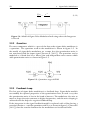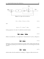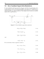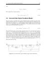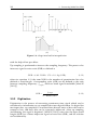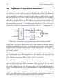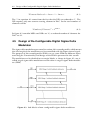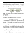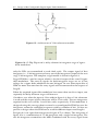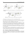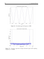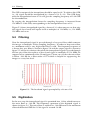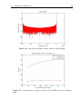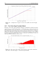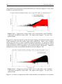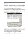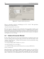
1
Institutionen för systemteknik Department of Electrical Engineering Examensarbete Design of an all-digital, reconfigurable sigma-delta modulator Examensarbete utfört i Elektroniksystem vid Tekniska högskolan vid Linköpings universitet av Sohaib A. Qazi and S. Asmat Ali Shah LiTH-ISY-EX--12/4557--SE Linköping 2012 Department of Electrical Engineering Linköpings universitet SE-581 83 Linköping, Sweden Linköpings tekniska högskola Linköpings universitet 581 83 Linköping Design of an all-digital, reconfigurable sigma-delta modulator Examensarbete utfört i Elektroniksystem vid Tekniska högskolan vid Linköpings universitet av Sohaib A. Qazi and S. Asmat Ali Shah LiTH-ISY-EX- -12/4557- -SE Handledare: Nadeem Afzal isy, Linköpings universitet Examinator: Dr. J. Jacob Wikner isy, Linköpings universitet Linköping, 17 maj 2012 Avdelning, Institution Division, Department Datum Date Avdelningen för Elektroniksystem Department of Electrical Engineering SE-581 83 Linköping 2012-05-17 Språk Language Rapporttyp Report category ISBN Svenska/Swedish Licentiatavhandling ISRN Engelska/English Examensarbete C-uppsats D-uppsats — LiTH-ISY-EX- -12/4557- -SE Serietitel och serienummer Title of series, numbering Övrig rapport ISSN — URL för elektronisk version http://urn.kb.se/resolve?urn=urn:nbn:se:liu:diva-XXXXX Titel Title Författare Author Design of an all-digital, reconfigurable sigma-delta modulator Sohaib A. Qazi and S. Asmat Ali Shah Sammanfattning Abstract This thesis presents a model of reconfigurable sigma-delta modulator. These modulators are intended for high speed digital Digital to Analog Converters. The modulators are intended to reduce complexity of current steering DACs and also considered as a front end of data converters. Quantization noise present in digital signal is pushed to higher frequencies by sigma-delta modulators. Noise in high band frequencies can be removed by a low pass filter. A test methodology involving generation of baseband signal, interpolation and digitization is opted. Topologies tested in MATLAB® include signal feedback and error feedback models of first-order and second-order sigma-delta modulators. Error feedback and signal feedback first-order modulators’ performance is quite similar. The SNR of a first-order error feedback model is 52.3 dB and 55.9 dB for 1 and 2 quantization bits, respectively. In second-order SDM, signal feedback provides best performance with 80 dB SNR. The other part of the thesis focuses on the implementation of the sigma-delta modulator (SDM) using faster time to market approach. SoC Encounter, a tool from Cadence, is the easiest way to do this job. The modulators are implemented in 65-nm technology. The reconfigurable sigma-delta modulator is designed using Verilog-HDL language. Switches are introduced to control the reconfigurable SDM for different input word lengths. Word-length can vary from 0 to 4 bits. Modulator is designed to work for frequencies of 2 GHz. To netlist the design, Design Compiler is used which is a tool from Synopsys®. The area of the chip reported by design compiler is 563.68 um. When the design is implemented in SoC Encounter, area of the chip is increased, because the core utilization, while designing, is only 60%, which is 556.8 um. Remaining 40% area is used by buffers, inverter and filler cells during clock tree synthesis. The buffers and inverters are added to remove the clock phase delay between different registers. Power consumption of the chip is 319 mW. Internal power of the modulators is 219.1 mW. Switching power of output capacitances is 99.9 mW, which is 31% of the total power consumed. Main concern of the power loss is considered to be power leakage. To reduce the leakage power and achieve high speed design CORE65GPHVT libraries are used. Leakage power of the design is 2.825 uW which is 0.00088% of the total power. Nyckelord Keywords problem, lösning Abstract This thesis presents a model of reconfigurable sigma-delta modulator. These modulators are intended for high speed digital Digital to Analog Converters. The modulators are intended to reduce complexity of current steering DACs and also considered as a front end of data converters. Quantization noise present in digital signal is pushed to higher frequencies by sigma-delta modulators. Noise in high band frequencies can be removed by a low pass filter. A test methodology involving generation of baseband signal, interpolation and digitization is opted. Topologies tested in MATLAB® include signal feedback and error feedback models of first-order and second-order sigma-delta modulators. Error feedback and signal feedback first-order modulators’ performance is quite similar. The SNR of a first-order error feedback model is 52.3 dB and 55.9 dB for 1 and 2 quantization bits, respectively. In second-order SDM, signal feedback provides best performance with 80 dB SNR. The other part of the thesis focuses on the implementation of the sigma-delta modulator (SDM) using faster time to market approach. SoC Encounter, a tool from Cadence, is the easiest way to do this job. The modulators are implemented in 65-nm technology. The reconfigurable sigma-delta modulator is designed using Verilog-HDL language. Switches are introduced to control the reconfigurable SDM for different input word lengths. Word-length can vary from 0 to 4 bits. Modulator is designed to work for frequencies of 2 GHz. To netlist the design, Design Compiler is used which is a tool from Synopsys®. The area of the chip reported by design compiler is 563.68 um. When the design is implemented in SoC Encounter, area of the chip is increased, because the core utilization, while designing, is only 60%, which is 556.8 um. Remaining 40% area is used by buffers, inverter and filler cells during clock tree synthesis. The buffers and inverters are added to remove the clock phase delay between different registers. Power consumption of the chip is 319 mW. Internal power of the modulators is 219.1 mW. Switching power of output capacitances is 99.9 mW, which is 31% of the total power consumed. Main concern of the power loss is considered to be power leakage. To reduce the leakage power and achieve high speed design CORE65GPHVT libraries are used. Leakage power of the design is 2.825 uW which is 0.00088% of the total power. iii Acknowledgments First of all, all the praise and gratitude is for Allah SWT, who gave us strength and courage to complete this thesis in time. We would like to thank our supervisor Mr. Nadeem Afzal who helped us through out our thesis work. A special thanks to our examiner Dr. J. Jacob Wikner for his kind support throughout our thesis. Mr J. Jacob Wikner’s several years of experience helped us to gain hands-on experience on different tools. The format of meetings was really very helpful to judge the progress of the thesis work. We also thank our seniors for their kind support throughout this thesis. We like to say thanks to our friends Muaz-un-Nabi, Shehryar Khan, Abdul Mateen Malik, Muhammad Suleman Khan and Muhammad Touqeer Pasha for proofreading our report. At the end thanks to our family especially our parents, without their prayers and support this would not even happen. Linköping, May 2012 Sohaib A. Qazi and S. Asmat Ali Shah v Contents List of Figures ix List of Tables xii Notation xv I Background 1 Introduction II 3 Sigma Delta Modulators 2 Sigma Delta Modulators 2.1 Introduction . . . . . . . . . . . . . . . . . 2.2 Signal Feedback Sigma Delta Modulators . 2.2.1 Accumulator . . . . . . . . . . . . . 2.2.2 Quantizer . . . . . . . . . . . . . . 2.2.3 Feedback Loop . . . . . . . . . . . . 2.3 Error Feedback Sigma Delta Modulators . 2.4 Second-Order Signal Feedback Model . . . 2.5 Conclusion . . . . . . . . . . . . . . . . . . III . . . . . . . . . . . . . . . . . . . . . . . . . . . . . . . . . . . . . . . . . . . . . . . . . . . . . . . . . . . . . . . . . . . . . . . . . . . . . . . . . . . . . . . . . . . . . . . . . . . . . . . . . . . . . . . . 9 9 10 11 12 12 14 15 16 . . . . . . . . . . . . . . . . . . . . . . . . . . . . . . . . . . . . . . . . . . . . . . . . . . . . . . . . . . . . . . . . . . . . . . . . . . . . . . . . . . . . 19 19 19 20 20 24 25 Processing Model for SDM 3 Processing Model for SDM 3.1 Introduction . . . . . . 3.2 Signal Generation . . . 3.3 Interpolation . . . . . . 3.3.1 Sampling . . . . 3.3.2 Digitization . . 3.4 Conclusion . . . . . . . . . . . . . . . . . . . . . . . . . . . . . . . . . . . . . vii . . . . . . . . . . . . . . . . . . . . . . . . . . . . . . . . . . . . viii IV CONTENTS Digital Modelling of SDM 4 Digital Modeling of SDM 4.1 Introduction . . . . . . . . . . . . . . . . . . . . . . . . . . 4.2 SoC Encounter Design Flow . . . . . . . . . . . . . . . . . 4.3 Design Libraries . . . . . . . . . . . . . . . . . . . . . . . . 4.4 Top Model of Sigma Delta Modulator . . . . . . . . . . . . 4.5 Design of Re-Configurable Digital Sigma Delta Modulator 4.5.1 Subtractor Module . . . . . . . . . . . . . . . . . . 4.5.2 Delay Stage . . . . . . . . . . . . . . . . . . . . . . 4.5.3 Integrators for Stage0 . . . . . . . . . . . . . . . . . 4.5.4 Extension of Stage0 for Re-Configurability . . . . . 4.5.5 Pipelining for Higher Number of Bits . . . . . . . 4.6 Modeling Language for SDM . . . . . . . . . . . . . . . . . 4.7 Test Methodology for Simulations . . . . . . . . . . . . . . 4.8 Testbench for Simulations . . . . . . . . . . . . . . . . . . 4.8.1 MATLAB Environment . . . . . . . . . . . . . . . . 4.8.2 Interfaces . . . . . . . . . . . . . . . . . . . . . . . . 4.8.3 Cadence Environment . . . . . . . . . . . . . . . . 4.9 Conclusion . . . . . . . . . . . . . . . . . . . . . . . . . . . . . . . . . . . . . . . . . . . . . . . . . . . . . . . . . . . . . . . . . . . . . . . . . . . . . . . . . . . . . . . . . . . . . . . . . . . . . . . . . . . . . . . . 29 29 29 31 32 33 34 34 34 36 38 38 40 40 42 42 43 44 . . . . . . . . . . . . . . . . . . . . . . . . . . . . . . . . . . . . . . . . . . . . . . . . . . . . . . . . . . . . . . . . . . . . . . . . . . . 47 47 47 47 49 49 50 52 53 54 55 55 57 57 59 59 6 SoC Encounter Manual 6.1 Introduction . . . . . . . . . . . . . . . . . . . . . . . . . . . . . . . 6.2 Behavioral Modeling (MODELSIM) . . . . . . . . . . . . . . . . . . 63 63 63 V Simulation Results 5 Simulation Results 5.1 Introduction . . . . . . . . . . . . . . . . . . . 5.2 Baseband Signal Generator . . . . . . . . . . . 5.3 Interpolation . . . . . . . . . . . . . . . . . . . 5.4 Filtering . . . . . . . . . . . . . . . . . . . . . 5.5 Digitization . . . . . . . . . . . . . . . . . . . . 5.6 Sigma Delta Modulators . . . . . . . . . . . . 5.6.1 First-Order Signal Feedback Model . . 5.6.2 First-Order Error Feedback Model . . 5.6.3 Second-Order Signal Feedback Model 5.6.4 Second-Order Error Feedback Model . 5.6.5 Comparison of Modulators . . . . . . . 5.7 Hardware Implementation Results . . . . . . 5.7.1 Area Consumed . . . . . . . . . . . . . 5.7.2 Power Utilization . . . . . . . . . . . . 5.8 Conclusion . . . . . . . . . . . . . . . . . . . . VI . . . . . . . . . . . . . . . . . . . . . . . . . . . . . . . . . . . . . . . . . . . . . . . . . . . . . . . . . . . . . . . . . . . . . . . . . . . . . . . . . . . . . . . . . . . . . . . . . . . . . . . . . SoC Encounter Manual 6.3 Synthesis and Netlist (Design Compiler) . . 6.3.1 Analyze Design . . . . . . . . . . . . 6.3.2 Elaborate Design . . . . . . . . . . . 6.3.3 Linking Design . . . . . . . . . . . . 6.3.4 Design Constraints . . . . . . . . . . 6.3.5 Compiling Design . . . . . . . . . . . 6.3.6 Design Reports . . . . . . . . . . . . 6.3.7 Verilog Netlist File . . . . . . . . . . 6.3.8 Timing and Design Constraints File . 6.4 Cadence Encounter Manual . . . . . . . . . 6.4.1 Importing Design . . . . . . . . . . . 6.4.2 Floor Planning the Design . . . . . . 6.4.3 Power Planning . . . . . . . . . . . . 6.4.4 Placing Standard Cells . . . . . . . . 6.4.5 Timing Optimization . . . . . . . . . 6.4.6 Finishing Design . . . . . . . . . . . 6.4.7 Checking Design . . . . . . . . . . . 6.4.8 Export Design . . . . . . . . . . . . . 6.5 Import Design Netlist in Cadence . . . . . . VII . . . . . . . . . . . . . . . . . . . . . . . . . . . . . . . . . . . . . . . . . . . . . . . . . . . . . . . . . . . . . . . . . . . . . . . . . . . . . . . . . . . . . . . . . . . . . . . . . . . . . . . . . . . . . . . . . . . . . . . . . . . . . . . . . . . . . . . . . . . . . . . . . . . . . . . . . . . . . . . . . . . . . . . . . . . . . . . . . . . . . . . . . . . . . . . . . . . . . . . . . . . . . . . . . . . . . . . . . . . . . . . . . . . . . . . . . . . . . . . . . . . . . . . 64 65 66 66 66 67 68 69 69 70 73 76 77 83 84 91 94 97 98 Conclusion and Future Work 7 Conclusion and Future Work 103 A IO Assignment File 105 B Configuration File 107 C Clock Tree Synthesis File 111 Bibliography 113 List of Figures 1.1 Spread noise over wide range of frequencies (a) Typical Nyquist conversion, (b) SDM noise spread . . . . . . . . . . . . . . . . . . . 1.2 Filtering the quantization noise in higher frequencies . . . . . . . . ix 3 4 x LIST OF FIGURES 1.3 Filtering technique used in modulator (a) High pass filter for baseband signal (b) Low pass filter for baseband signal . . . . . . . . . 2.1 2.2 2.3 2.4 2.5 2.6 2.7 2.8 3.1 3.2 3.3 3.4 3.5 3.6 3.7 3.8 3.9 4.1 4.2 4.3 4.4 4.5 4.6 4.7 4.8 4.9 4.10 4.11 4.12 4.13 4.14 4.15 Basic sigma-delta modulator. . . . . . . . . . . . . . . . . . . . . . . First-order sigma-delta modulator. . . . . . . . . . . . . . . . . . . Integrator stage of sigma-delta modulator. . . . . . . . . . . . . . . Model of Sigma Delta Modulator Indicating where the Integrator is Placed. . . . . . . . . . . . . . . . . . . . . . . . . . . . . . . . . . Quantizer stage of SDM. . . . . . . . . . . . . . . . . . . . . . . . . Sigma-delta modulator. . . . . . . . . . . . . . . . . . . . . . . . . . Error feedback sigma-delta modulator. . . . . . . . . . . . . . . . . Second-order signal feedback sigma-delta modulator . . . . . . . . 5 9 10 11 12 12 13 14 15 Design flow for thesis. . . . . . . . . . . . . . . . . . . . . . . . . . . Process of sampling the signal. . . . . . . . . . . . . . . . . . . . . . Graphical explanation of sampling process. . . . . . . . . . . . . . Input signal in time domain and frequency domain. . . . . . . . . Frequency spectrum of sampled data. . . . . . . . . . . . . . . . . . Concept of aliasing. . . . . . . . . . . . . . . . . . . . . . . . . . . . Interpolation. . . . . . . . . . . . . . . . . . . . . . . . . . . . . . . Steps involved in interpolation. . . . . . . . . . . . . . . . . . . . . Interpolation and sampling, (a) Baseband signal, (b) Interpolation, (c) Recovered signal. . . . . . . . . . . . . . . . . . . . . . . . . . . . 20 20 21 22 22 23 23 24 Steps involved in designing layout using SoC Encounter. . . . . . . Controlled, re-configurable sigma-delta modulator (SDM). . . . . Sub-blocks of non-configurable sigma-delta modulator. . . . . . . Architecture of stage0 sigma-delta modulator with integrators and a subtractor. . . . . . . . . . . . . . . . . . . . . . . . . . . . . . . . Architecture of 1-bit subtractor module. . . . . . . . . . . . . . . . D-Flip Flop used as delay element in integrator stage of sigmadelta modulator. . . . . . . . . . . . . . . . . . . . . . . . . . . . . . Internal structure of integrators. (a) 2-bit integrator and (b) 3-bit integrator. . . . . . . . . . . . . . . . . . . . . . . . . . . . . . . . . Internal structure of stage0 sigma-delta modulator. . . . . . . . . . Splitting 3-bit integrator in two stages, one stage is 2-bit wide and other is 1-bit. (a) Non-controlled splitting (b) Controlled splitting. Structure of stageN used for extension of stage0 for high order SDM. Top symbol of re-configurable sigma-delta modulator. . . . . . . . Architecture of reconfigurable sigma-delta modulator. . . . . . . . MODELSIM test-bench. . . . . . . . . . . . . . . . . . . . . . . . . . Test methodology for re-configurable SDM using MATLAB and Cadence. . . . . . . . . . . . . . . . . . . . . . . . . . . . . . . . . . . . MATLAB environment (a) Generate baseband signal, (b) Post processing after simulations. . . . . . . . . . . . . . . . . . . . . . . . . 30 32 33 25 34 35 35 36 36 37 38 38 39 40 41 42 LIST OF FIGURES 4.16 Interface between MATLAB and Cadence (a) Read-in data from MATLAB, (b) Write-out data from Cadence. . . . . . . . . . . . . . 4.17 Test-bench for real time simulations in Cadence. . . . . . . . . . . xi 43 43 5.1 Baseband signal of frequency 8 MHz. . . . . . . . . . . . . . . . . . 5.2 Frequency spectrum of input baseband signal with sampling frequency at 128 MHz. . . . . . . . . . . . . . . . . . . . . . . . . . . . 5.3 The baseband signal upsampled by a factor of 16. . . . . . . . . . . 5.4 Frequency response of anti-aliasing filter with order of 974. . . . . 5.5 Spectrum of output signal after anti-aliasing filter. . . . . . . . . . 5.6 Spectrum of digital signal with 16 word-length. . . . . . . . . . . . 5.7 Comparison of signal to noise ratio (SNR) and over sampling ratio. 5.8 Comparison of signal to noise ratio (SNR) and word-length (NOB). 5.9 Spectrum of first-order signal feedback sigma-delta modulator with OSR = 64, word-length = 16 and 2-bit quantization. . . . . . . . . 5.10 Spectrum of first order error feedback sigma-delta modulator with OSR = 64, word-length = 16 and 2-bit quantization. . . . . . . . . 5.11 Spectrum of second-order signal feedback sigma-delta modulator with OSR = 64, input word-length = 16 and 2-bit quantization. . . 5.12 Spectrum of second-order error feedback sigma-delta modulator with OSR = 64, input word-length = 16 and 2-bit quantization. . . 5.13 Comparison of first-order and second-order signal feedback sigmadelta modulator with OSR = 64, input word-length = 16 and 2-bit quantization. . . . . . . . . . . . . . . . . . . . . . . . . . . . . . . . 5.14 Comparison of first-order and second-order error feedback sigmadelta modulator with OSR = 64, input word-length = 16 and 2-bit quantization. . . . . . . . . . . . . . . . . . . . . . . . . . . . . . . . 5.15 Comparison of First-Order Signal and Error Feedback Sigma Delta Modulator with OSR = 64, Input Word-length = 16 and 2-bit Quantization. . . . . . . . . . . . . . . . . . . . . . . . . . . . . . . . . . . 5.16 Comparison of second-order signal and error feedback sigma-delta modulator with OSR = 64, input word-length = 16 and 2-bit quantization. . . . . . . . . . . . . . . . . . . . . . . . . . . . . . . . . . . 48 6.1 6.2 6.3 6.4 6.5 6.6 6.7 6.8 65 67 68 69 70 71 73 Set-up design parameters for analysis. . . . . . . . . . . . . . . . . Symbol of top level design schematic for sigma-delta modulator. . Parameters set-up for clock specification. . . . . . . . . . . . . . . . Setting design constraints for design . . . . . . . . . . . . . . . . . Compile window parameters. . . . . . . . . . . . . . . . . . . . . . Gate level schematic of 4-bit sigma-delta modulator. . . . . . . . . Data model of syn2tlf. . . . . . . . . . . . . . . . . . . . . . . . . . Design import window with parameters to set-up to import design in Encounter. . . . . . . . . . . . . . . . . . . . . . . . . . . . . . . . 6.9 Design imported in Encounter with rows of the core area. . . . . . 6.10 Set-up parameters for floor planning. . . . . . . . . . . . . . . . . . 6.11 Complete floor planned design including IO ports in place. . . . . 48 49 50 50 51 51 52 52 53 54 55 56 56 57 58 74 75 77 78 6.12 Global net connection window. . . . . . . . . . . . . . . . . . . . . 6.13 Set-up parameters to place power rings around the core. . . . . . . 6.14 Selecting power rails around the core. (a) Worst selection, (b) Best selection. . . . . . . . . . . . . . . . . . . . . . . . . . . . . . . . . . 6.15 Design with added rails around the core. . . . . . . . . . . . . . . . 6.16 Parameter set-up to add power stripes through the core. . . . . . . 6.17 Design including power stripes within core. . . . . . . . . . . . . . 6.18 SRoute window to route power nets. . . . . . . . . . . . . . . . . . 6.19 Placing standard cells in design. . . . . . . . . . . . . . . . . . . . . 6.20 Core area with standard cells placed. . . . . . . . . . . . . . . . . . 6.21 Design optimization window with pre-CTS, post-CTS and post-Route options. . . . . . . . . . . . . . . . . . . . . . . . . . . . . . . . . . . 6.22 Clock tree synthesis (CTS) window. . . . . . . . . . . . . . . . . . . 6.23 Selecting buffers and inverters to generate clock tree specification (*.ctstch) file. . . . . . . . . . . . . . . . . . . . . . . . . . . . . . . . 6.24 Display clock tree window to display phase delay and clock tree. . 6.25 Clock phase delay variation is shown in different colors. . . . . . . 6.26 Nano router settings. . . . . . . . . . . . . . . . . . . . . . . . . . . 6.27 Adding fillers in design. (a) Selected fillers for placement, (b) Filler select window. . . . . . . . . . . . . . . . . . . . . . . . . . . . . . . 6.28 Complete routed design after nano router. . . . . . . . . . . . . . . 6.29 Complete design with place & routed and empty spaces filled. . . 6.30 Settings for geometry verification. . . . . . . . . . . . . . . . . . . . 6.31 Verifying connectivity of design. . . . . . . . . . . . . . . . . . . . . 6.32 Export design to a *.gds file. . . . . . . . . . . . . . . . . . . . . . . 6.33 Import netlist design in Cadence for simulations. . . . . . . . . . . 79 80 81 82 83 84 85 85 86 87 87 88 89 90 91 92 93 94 95 96 97 99 List of Tables 5.1 Comparison of SNR for different quantization bits in first-order signal feedback SDM. . . . . . . . . . . . . . . . . . . . . . . . . . . 5.2 Comparison of SNR for different quantization bits in first-order error feedback SDM. . . . . . . . . . . . . . . . . . . . . . . . . . . 5.3 Comparison of SNR for different quantization bits in second-order signal feedback SDM. . . . . . . . . . . . . . . . . . . . . . . . . . . 5.4 Comparison of SNR for different quantization bits in second-order error feedback SDM. . . . . . . . . . . . . . . . . . . . . . . . . . . 5.5 Area of design (netlist). . . . . . . . . . . . . . . . . . . . . . . . . . xii 53 54 54 55 57 LIST OF TABLES xiii 5.6 Chip core area. . . . . . . . . . . . . . . . . . . . . . . . . . . . . . . 5.7 Power utilization. . . . . . . . . . . . . . . . . . . . . . . . . . . . . 58 59 6.1 Registers indicated by elaborate process. . . . . . . . . . . . . . . . 6.2 Summary of optimized design after pre-CTS . . . . . . . . . . . . . 66 85 Notation Notations Abbreviation SDM MSB LSB DRC DAC HVT LVT RTL CTS WNS LEF SNR OSR CT SOSDM Significance Sigma Delta Modulator Most Significant Bit Least Significant Bit Design Rule Check Digital to Analog Converter High Voltage Temperature Low Voltage Temperature Register Transfer Language Clock Tree Synthesis Worst Negative Slack Library Exchange Format Signal to Noise Ratio Oversampling Ratio Clock Tree Second Order Sigma Delta Modulator xv Part I Background 1 Introduction The sigma-delta converters have been in use for many years but the recent advancement in the technology has made it possible to use them widely. We can find the applications of these converters in homes such as communication systems, consumer and professional audio and precision measurement devices. One of the key properties of these converters is that they are the only one low cost conversion method which will provide a high dynamic range and flexibility in converting narrow-band signals. While understanding the operation of sigma delta converters; the key areas which need to be addressed are oversampling (interpolation), digital filtering, noise shaping and decimation, which are discussed in chapter 2. (a) (b) Figure 1.1: Spread noise over wide range of frequencies (a) Typical Nyquist conversion, (b) SDM noise spread 3 4 1 Introduction The interpolation will be carried out in two steps; up sampling and filtering. When the signal is oversampled it means that the sampling rate (sampling frequency) has been increased by inserting zeros, then the signal should be limited to a band by using a digital low pass filter. The desired response of the digital filter should be set such that the output signal has same spectral contents as that of the input signal. So the transfer function HL (f ) of an interpolation filter is characterized by 1, 0, f 0 < f < 2si fsi Lfsi 2 <f < 2 (1.1) Where ‘fsi0 is the sampling frequency and ‘L’ is an up sampling factor. By taking samples at a much higher rate we are not changing the signal and quantization noise power; however the quantization noise power is spread over a larger frequency range. So it decreases the spectral density of the quantization noise. Now if comparison is made with the original Nyquist rate the quantization noise power is reduced by 3 dB for every doubling of the oversampling ratio (OSR) as discussed in section 3.3.2. In this way oversampling decreases the quantization noise in the band of interest. Figure 1.1 shows the concept of spreading the noise over a larger frequency range and a typical Nyquist type converter [Jarman [1995]]. (a) (b) Figure 1.2: Filtering the quantization noise in higher frequencies One of the advantages of using oversampling ratio is that the image frequencies can be moved away from the signal of interest and then we can use a less complex low cost filter that has a wider transition band. An essential factor, that makes sigma-delta modulator (SDM) more attractive is noise shaper or integrator which distributes the noise in such a way that is very low in the intended signal or at the lower frequencies as shown in figure 1.2a. With the help of a digital low pass filter, sharp cutoff (edges) at the band of interest will be defined which will be helpful for removing out of band quantization noise and also the unwanted signals or images. Figure 1.2b demonstrates the idea of digital filtering. 5 The sigma-delta modulators tend to push the noise from the band of interest to a higher frequency band. So the modulator acts like a low pass filter for input signal (figure 1.3a) and a high pass filter for noise part as shown in figure 1.3b. A detailed analysis of how the noise is pushed to higher frequencies is explained in chapter 2. (a) (b) Figure 1.3: Filtering technique used in modulator (a) High pass filter for baseband signal (b) Low pass filter for baseband signal Part II Sigma Delta Modulators 2 Sigma Delta Modulators 2.1 Introduction Sigma-delta modulators are considered to be at the front end of the data converters. Digitization is carried out in two steps, i.e., sampling and quantization. When a signal is digitized a quantization error is introduced. Sigma-delta modulator moves the quantization noise to higher frequencies. After the modulator, a low pass filter can be used to extract the original signal. This chapter will present a detailed discussion about the sigma-delta modulators. A generalized structure of this sigma-delta modulator consists of a digital signal as an input, an integrator, a quantizer and a feedback loop as shown in figure 2.1. Figure 2.1: Basic sigma-delta modulator. There are different topologies involved in sigma-delta modulators, like signal feedback and error feedback models. Both topologies are discussed in detail in 9 10 2 Sigma Delta Modulators the following sections of this chapter. 2.2 Signal Feedback Sigma Delta Modulators As depicted in figure 2.2, for signal feedback model, output signal is fed back and subtracted from the input of the modulator. The model for the signal feedback consists of an input signal X[n], eQ defines the quantization bits and Y[n] is the output of the modulator. Figure 2.2: First-order sigma-delta modulator. The mathematical modeling of figure 2.2 is given by the following equations X1 [n] = X[n] − Y [n], (2.1) X2 [n] = X1 [n] + X2 [n − 1], (2.2) Y [n] = X2 [n − 1] + eQ . (2.3) and Taking the z-transform of the equations (2.1, 2.2 and 2.3) will give and X1 (z) = X(z) − Y (z), (2.4) X2 (z) = X1 (z) + X2 (z).z −1 , (2.5) 2.2 Signal Feedback Sigma Delta Modulators Y (z) = X2 (z)z −1 + eQ 11 (2.6) output, respectively. The output Y(z) of the model is calculated by solving the equations (2.4, 2.5 and 2.6) in terms of X(z) and eQ . The output Y(z) is given by Y (z) = Y (z) = X(z)z −1 + eQ (1 − z −1 ). 2.2.1 (2.7) Accumulator An integrator shown in figure 2.3, consists of an adder and a delay element, is a part of signal feedback model. The adder accumulates delayed output with the next input of the sigma-delta modulator. Figure 2.3: Integrator stage of sigma-delta modulator. The integrator can be described by the difference equations X1 [n] = X[n] + Y [n] (2.8) Y [n] = X1 [n − 1]. (2.9) and Taking the z-transform will result in X1 (z) = X(z) + Y (z) (2.10) Y (z) = X1 (z)z −1 . (2.11) and Solving (2.10 and 2.11) yields the transfer function 12 2 Sigma Delta Modulators Y (z) z −1 . = X(z) 1 − z −1 (2.12) Figure 2.4: Model of Sigma Delta Modulator Indicating where the Integrator is Placed. 2.2.2 Quantizer The next component which is a part of the first-order sigma-delta modulator is a quantizer. The quantizer used in the modulator is shown in figure 2.5. In the model of sigma-delta modulator we assume that the quantization noise is not correlated with the input signal [Janssen E. [2011]]. The quantizer can be modeled as a block that has a linear gain and independent noise source which adds quantization noise as shown in figure 2.5. Figure 2.5: Quantizer stage of SDM. 2.2.3 Feedback Loop The last part of sigma-delta modulator is a feedback loop. Sigma-delta modulators modify the spectral properties of the quantization noise, in such a way that the quantization noise is low in the band of interest. The modulator also tries to move or shape the noise contents to higher frequencies, and this noise shaping is achieved with the help of a negative feedback loop. If the integrator in the signal feedback model is replaced with a filter having a transfer function z −1 and the quantizer with N(z) as shown in figure 2.6 [Janssen E. [2011]]; then the transfer function for the modulator can be derived from 2.2 Signal Feedback Sigma Delta Modulators 13 Figure 2.6: Sigma-delta modulator. Y (z) = ((X)(z) − Y (z))(z −1 ) + N (z) (2.13) Y (z)(1 + z −1 ) = X(z)z −1 + N (z). (2.14) and Solving equations 2.14 and 2.15 yields the transfer function Y (z) N (z) z −1 = + . X(z) 1 + z −1 1 + z −1 (2.15) When we consider N(z) = 0, in equation 2.15 and solve for Y (z)/X(z), will give us Y (z) z −1 = . X(z) 1 + z −1 (2.16) Equation 2.16 shows that the modulator acts like a low pass filter for the input signal. Similarly, replacing X(z) with zero in equation 2.15, and solving for Y(z)/N(z) yields in Y (z) 1 = N (z) 1 + z −1 (2.17) which realizes that the modulator is working as a high pass filter for the noise. 14 2.3 2 Sigma Delta Modulators Error Feedback Sigma Delta Modulators In error feedback model presented in [Lovgren [2001]]; the quantization noise or quantization error is fed back and added to the input of the modulator as depicted in figure 2.7. In error feedback model, quantizer input eQ defines output word-length for sigma-delta modulator. The complete flow of the error feedback model can be represented by Figure 2.7: Error feedback sigma-delta modulator. X1 [n] = X[n] + Y2 [n], (2.18) Y [n] = X1 [n] + eQ , (2.19) Y1 [n] = X1 [n] + Y [n], (2.20) Y2 [n] = Y1 [n − 1]. (2.21) and The z-transform of above equations results in X1 (z) = X(z) + Y2 (z), (2.22) Y (z) = X1 (z) + eQ , (2.23) Y1 (z) = X1 (z) + Y (z), (2.24) 2.4 Second-Order Signal Feedback Model 15 and Y2 (z) = Y (z)Z −1 . (2.25) The output Y(z) is represented as Y (z) = X(z) + eQ (1 − z −1 ). 2.4 (2.26) Second-Order Signal Feedback Model Figure 2.8 shows a second-order signal feedback model, in which two first-order signal feedback models are cascaded. In second-order model two additional scaling factors are involved, i.e., two multipliers whose lengths can be varied from ‘zero’ to ‘one’ depending upon the requirements. The transfer function for secondorder signal feedback model is given by Y (z) = X(z)z −1 + E(z)(1 − z −1 )2 . (2.27) The modulator for the second-order apprehend that the signal transfer function is Hx (z) = z −1 and the noise transfer function is N (z) = ((l − z −1 ))2 . It is obvious from equation 2.27, that the noise suppression in case of the second-order modulator is more in the lower frequency band, and noise is amplified more outside the band of interest. While comparing with first-order noise power is pushed more outside the band of interest, i.e., the signal band. Figure 2.8 depicts two integrators used in the model, where the transfer function of the first integrator is 1/(1 − z −1 ) and the second integrator has the transfer function z −1 /(1 − z −1 ) [Pervez M. Aziz [1996]]. Figure 2.8: Second-order signal feedback sigma-delta modulator 16 2.5 2 Sigma Delta Modulators Conclusion In this chapter different topologies of sigma-delta modulators were discussed. The discussion is based on a detailed analysis of various components within the sigma-delta modulators. Part III Processing Model for SDM 3 Processing Model for SDM 3.1 Introduction Testing and comparing results of the modulators are the important parts of this thesis. Without verification of the modulators, it is hard to choose between different available modulator topologies. This chapter presents a complete processing model for the modulators which includes, baseband signal generation, interpolation of the signal, digitizing up-sampled signal and simulating the modulators. 3.2 Signal Generation In signal generation block a continuous time coherent signal is generated and that signal can be characterized by X(t) = Asin(2πf t + φ), (3.1) where ‘A’ is the amplitude which defines voltage swing of sine function, ‘f’ is the frequency corresponding to the number of times a signal repeats itself in unit time and φ represents the phase of the signal. There are some other parameters related to the signal; one of them is bandwidth. The bandwidth can also be defined as range of frequencies an electronic signal uses over an electronic medium for its transmission. 19 20 3 Processing Model for SDM Figure 3.1: Design flow for thesis. 3.3 Interpolation Interpolation is a process of increasing the sampling frequency. Interpolation consist of two steps; first to increase input sampling rate by inserting zeros in between existing samples, called as zero stuffing. The second step is to band limit the signal using a digital low pass filter. 3.3.1 Sampling Sampling is a process of converting a continuous time signal to a discrete time signal, simply multiplying a continuous time signal to an impulse train will give sampled data. The impulse train is defined mathematically as ∆T (t) = ∞ X δ(t − nT ), (3.2) n=−∞ where delta function δ(t) can be defined by the relation 1, 0, t=0 elsewhere (3.3) Impulse train, in equation 3.2, is represented by delayed versions of delta function. In the equation 3.2 ‘n’ is integer value and ‘T’ is the sampling period. The process of sampling is shown in figure 3.3. Figure 3.2: Process of sampling the signal. Figure 3.2 demonstrates graphical model for sampling. Figure 3.3 elaborates the graphical steps involved in sampling, in order to achieve sampled data at the output. 3.3 21 Interpolation Figure 3.3: Graphical explanation of sampling process. Figure 3.2 and figure 3.3 explains graphical steps involved in sampling. For detailed mathematical analysis, sampled signal can be represented by Xs (t) = X(t)δT (t), (3.4) where Xs (t) is the sampled output, X(t) is the continuous signal and δT (t) is the impulse train. Now substituting value of δT (t) from equation 3.2 in equation 3.4 will result in sampled signal in time domain as Xs (t) = ∞ X X(t)δ(t − nT ). (3.5) n=−∞ In time domain these signals are multiplied while in frequency domain these signals are convolved. For frequency domain analysis, the Fourier transform is used and the Fourier transform of equation 3.5 is Xs (jΩ) = 1 X(jΩ)δT (iΩ) 2π (3.6) and the Fourier transform of the impulse train is δT (jΩ) = ∞ 2π X δ(Ω − nΩs ). T n=−∞ Substituting value from equation 3.7 to equation 3.6 will result in (3.7) 22 3 Processing Model for SDM ∞ 1 X X(j(Ω − nΩs )). Xs (jΩ) = T n=−∞ (3.8) Equation 3.8 defines the Fourier transform of input signal and shows that the images are replicated at integer multiples of sampling frequency. The Fourier transform of the input signal is shown in figure 3.4. Figure 3.4: Input signal in time domain and frequency domain. The mathematical behavior defined in equation 3.8 can be demonstrated graphically by figure 3.5. Observe input spectrum is repeating itself at integer multiples of sampling frequency. Figure 3.5: Frequency spectrum of sampled data. For sampling a signal there are some limitations and constraints. If these limitations and constraints are not satisfied then the reconstruction of sampled signal is not possible. One of the constraints is that, the sampling frequency should be twice the highest frequency component of the input signal, i.e., defined by the Nyquist criteria. When the said condition is satisfied then resulted signal will look like as shown in figure 3.5. If this condition is not fulfilled then aliasing will occur, and lower side band of the first spectrum will interfere with upper side band of the second spectrum laying near at integer multiples of sampling frequency and consequently the original information cannot be recovered, as shown in figure 3.6. Interpolation consists of two steps; first is up sampler in which continuous time signal sampled at a much higher rate than the Nyquist rate and second step is filtering. Figure 3.7 shows the steps involved in interpolation. Interpolation by a factor of ‘L’ is performed by inserting ‘L-1’ zeros in between each pair of samples of the input signal. Then a low pass filter is used to get the desired sample having pass band edge at ‘pi/L’, and filter will remove all mirrored frequency components of the signal. Figure 3.8 presents the graphical 3.3 23 Interpolation Figure 3.6: Concept of aliasing. Figure 3.7: Interpolation. concept of interpolation when a continuous time signal is interpolated by a factor of ‘L’ equals to “three”. Figure 3.8 shows x(n) which is achieved through uniform sampling in which the sampling frequency is fs = 1/T , i.e., x(n) = xc (nT ). From x(n) a new sequence is obtained in which the sampling frequency is ‘L’ times higher than the uniform sampling, i.e., Y (m) = xc (mT /L). The sampling period for the signal x(n) was ‘T’, and now after interpolation the sampling period for w(m) is reduced to T 1 = T /L [Lowenborg [2006]]. For frequency domain analysis the Fourier transform of w(m) is given by W (e jωT1 ) = ∞ X w(m)e−jωT1 m , (3.9) m=−∞ the Fourier transform of W(n) in terms of x(n) is represented as W (e jωT1 ) = ∞ X x(n)e−jωT1 Ln . (3.10) n=−∞ and the Fourier transform of signal x(n) is given by X(e jωT ) = ∞ X x(n)e−jωT n . (3.11) n=−∞ Figure 3.9 from [Lowenborg [2006]] shows graphical steps involved in interpolation, initially the signal is interpolated by a factor of L, and then digitally filtered 24 3 (a) Processing Model for SDM (b) (c) Figure 3.8: Steps involved in interpolation. with the help of low pass filter. Up sampling is performed to increase the sampling frequency. The process also increases signal to noise ratio (SNR) as defined as SN R = 6.02 · N OB + 1.76 + 10 · log(OSR), (3.12) where in equation 3.12 the term NOB is the number of quantization bits also defined as word-length. Oversampling ratio (OSR) can be defined as the ratio 0 between sampling frequency ‘fsample and base band signal bandwidth [Afzal N [2010]] OSR = 3.3.2 fsample 2 · “Bandwidth00 . (3.13) Digitization Digitization is the process of converting continuous time signal which can be considered as information or up sampled data into digital format. In digital format input data (up sampled) is structured into discrete units of data that can be termed as bits, and those bits can be separately addressed. After up sampling and filtering, the signal is digitized. [Afzal N [2010]] states that the input wordlength (NOB) has a direct impact on signal to noise ratio (SNR), and the relation can be defined by 3.4 25 Conclusion (a) (b) (c) Figure 3.9: Interpolation and sampling, (a) Baseband signal, (b) Interpolation, (c) Recovered signal. SN R = 6.02 · N OB + 1.76. (3.14) Equation 3.14 realizes the fact that if word-length (NOB) is increased, the SNR will increase by a factor of 6 dB. 3.4 Conclusion In this chapter the process, that defines the input signal to the sigma-delta modulator, is discussed in detail. This process includes base band signal generation, up sampling, filtering and quantization. Part IV Digital Modelling of SDM 4 Digital Modeling of SDM 4.1 Introduction This chapter discusses digital modeling of the sigma-delta modulators which are described in chapter 2. The aim of this thesis is to implement a reconfigurable sigma delta modulator in hardware. The hardware implementation of sigma delta modulator means the design is implemented using automatically generated layouts. The layout design is quite laborious which requires long design time if done manually. To skip the manual layout design process and minimize design effort; a design tool from Cadence® named SoC Encounter is used. This tool minimizes the effort of layout design by automatically generating layout design from Verilog netlist. 4.2 SoC Encounter Design Flow In this thesis, a reconfigurable sigma-delta modulator is designed, which is a part of all-digital DACs. The sigma-delta modulator is designed using RTL language, i.e., Verilog. SoC Encounter is then used to generate a layout design from Verilog netlist, generated by a tool named Design Compiler. The complete design flow of SoC Encounter is shown in figure 4.1. Encounter has three types of input files; one is Verilog netlist file which is generated using a Design Compiler. The Design Compiler is an RTL synthesis tool from Synopsys which is used to convert RTL design file into Verilog netlist. The compiler takes care of the timing information and the standard cells that will be placed during layout generation process. The second input is timing information 29 30 4 Digital Modeling of SDM Figure 4.1: Steps involved in designing layout using SoC Encounter. 4.3 Design Libraries 31 file (*.tlf), which contains timing information of the standard cells available in current standard cells library; provided by the foundry. The last file used to import design in Encounter is Library Export Format (LEF) file. These files contain definitions of routing layers, vias, metal capacitances and design rules etc. In the second step, floor planning is performed. While floor planning one should know available core size, size of the chip and location of IO ports. The floor plan defines outer boundaries of the chip being designed. Power planning step defines how power will be distributed throughout the chip. There are several ways to distribute power in chip, which are explained in detail in section 6.4.3 of chapter 6. In the next step the standard cells are placed and optimized for timing. Any differences in clock phase delays will be removed in this step by adding inverters and buffers in design. The design is then routed and once again checked for the clock phase delays. After routing and optimizing design for the timing constraints it is necessary to verify the design. There are several verification options available like connectivity verification, geometry verification and design rule check (DRC) verification to verify successful placement of the design. After successful verification of the design, final step is to export the design in *.gds file and netlist (*.v) file. This new netlist also contains the inverters and buffers added in timing optimization process. The *.gds file can be used to import layout in cadence and both netlist files can be used to import design schematic in cadence. 4.3 Design Libraries While working with Encounter; the choice of libraries is one of the critical steps of designing. Several libraries are available in Encounter kit with different specifications of power, voltage, speed and leakage; some of the available libraries are GPHVT, GPLVT, GPSVT, LPHVT, LPLVT and LPSVT. GP libraries are the fastest libraries while the LVT libraries provide good performance at high data rates. There is a trade-off between speed and power leakage. With increase in the speed, the leakage will also be increased. So the HVT options typically give best performance in terms of speed and power leakage [Pullini. A [2007]]. The modulators presented in this thesis are intended to be used with high speed applications. Leakage is desired to be reduced for high speed applications; so the libraries used in this thesis were from CORE65GPHVT library. GP are the fastest and HVT will provide the best performance as compared with speed. 32 4.4 4 Digital Modeling of SDM Top Model of Sigma Delta Modulator The digital DACs need to operate at high frequencies. For high speed operations it is critical to achieve high precision, resolution and accuracy. Resolution of the DACs depends on input word-length of the DAC. The complexity of a DAC greatly depends on number of current steering elements which will be used for the DAC [Jui-Yuan Yu [2006]]. The current steering elements are considered in this thesis as this thesis is a sub-project of All-Digital Current Steering DACs (STUCK) at Linköing University. The number of current steering elements used in a DAC depends on input word-length of the DAC. Current steering elements are increased by power of ‘2’ if number of bits are increased. For a 8 bit wordlength DAC; number of current steering elements will be 28 − 1; which are 255. Figure 4.2: Controlled, re-configurable sigma-delta modulator (SDM). Digital DACs are hard to design with such a high number of elements because of the design complexity and area. The model presented in this report reduces word-length; that will be the input of the current steering DACs. In figure 4.2, a model is presented which will generate a weighted output with less number of bits [Noli S. [2009]]. The bit splitter, shown in figure 4.2, is used to separate MSBs and LSBs. Since this is a reconfigurable sigma-delta modulator, so the number of bits split will vary depending on the control signal. The least significant bits can be varied from ‘0’ to ‘4’; which means that the MSBs will be ‘8’ to ‘4’, respectively. The sigma-delta modulator will take the LSBs and will accumulate them to generate a weighted output. In figure 4.8 there is only one delay element in critical path of second-order sigma-delta modulator. This also means that the sigmadelta modulator takes one extra clock cycle to accumulate and generate output. The path of MSBs does not have any delay which causes the mismatch in phase delays. To balance out this phase delay difference; a delay is added in path of MSBs. At the last stage, MSBs and LSBs are added together to generate an output of MSB+1 bits; the number of bits is quite less than the original number of bits. So the number of current steering elements of DAC are reduced by 4.5 Design of Re-Configurable Digital Sigma Delta Modulator “ElementsReduced 00 = 2N OB − 1 − 2MSB+1 . 33 (4.1) The ‘1’ in equation 4.1 comes from the fact that the LSBs are reduced to ‘1’. The LSB requires only one current steering element in DAC. So the total number of elements will be “N umberof Elements00 = 2MSB+1 . (4.2) In figure 4.2 consider MSBs and LSBs are ‘4’; so reduced number of elements for DAC are 32. 4.5 Design of Re-Configurable Digital Sigma Delta Modulator The sigma-delta modulator presented in section 4.4 is reconfigurable, which means that the length of the modulator can be controlled with the input control signal. The purpose of this reconfigurable SDM is to use same SDM for different input word lengths. Functionality and design of the SDM is presented in this section. The modulator can be divided in two major blocks as shown in figure 4.3, one is called stage0 sigma-delta modulator and the other is stageN sigma-delta modulator (SDM). Figure 4.3: Sub-blocks of non-configurable sigma-delta modulator. 34 4 Digital Modeling of SDM Stage0 of SDM has one bit input, which is MSB of the input signal that is passed to the sigma-delta modulator. The stage0 of SDM shown in figure 4.4, has three submodules named subtractor, 2-bit integrator and last module is 3-bit integrator. The accumulated output is fed back to the subtractor and is subtracted from the input signal. The output of the subtractor is fed to a 2-bit accumulator which will accumulate the signal and result of accumulation is passed to a 3-bit integrator. Figure 4.4: Architecture of stage0 sigma-delta modulator with integrators and a subtractor. 4.5.1 Subtractor Module The subtractor is modeled using simple 2’s complement logic. In 2’s complement logic a subtractor is designed using an adder; which is explained by Out = in1 − in2 = in1 + (in2 + Cin ). (4.3) In equation 4.3, input in2 is inverted and fed to the adder which is only 1’s complement of the in2 signal. In figure 4.5 the carry in signal Cin of the adder is set to ‘1’, i.e., high voltage, so that the inverted signal can be converted to 2’s complement. The two’s complement signal is added to input in1 to get the 2-bit subtracted output. 4.5.2 Delay Stage The delay stage of an integrator is modeled as a D-Flip Flop. The reset signal is active high which means output of the flip flop will be set to zero when the reset signal is high; otherwise will work normally. A normal operation of a flip-flop is to hold the input data for a single clock cycle and send to output when next positive clock edge is detected. 4.5.3 Integrators for Stage0 The stage0 uses two types of integrators; one is a 2-bit integrator and the other is a 3-bit integrator, since 2-bit and 3-bit adders were used in integrators and are shown in figure 4.7a & figure 4.7b. The output of each integrator is accumulated with input at next clock cycle. In integrator MSB is considered to be the carry bit and is not fed back to the adder, 4.5 Design of Re-Configurable Digital Sigma Delta Modulator 35 Figure 4.5: Architecture of 1-bit subtractor module. Figure 4.6: D-Flip Flop used as delay element in integrator stage of sigmadelta modulator. only the LSBs are accumulated at each clock cycle. The output signal of first integrator, i.e., 2-bit integrator and carry out of the integrator is input of the next stage 3-bit integrator. The complete stage0 model is shown in figure 4.8. Stage0 SDM has a one bit output which is also final output of the overall sigmadelta modulator. The carry-in signals for both integrator stages are set to low voltage for a sigma-delta modulator for one bit input. In case when input bits of SDM are more than one then the carry signals will be connected to the outputs of StageN. When the required sigma-delta modulator have more than one bit as input, consequently the delay between stages will increase. Consider a case when the input is 2 bits wide in figure 4.8, then a 2 bit subtractor is used and the output of the subtractor will be 3 bits wide. The two integrators required in this case will be 3 and 4 bits wide, respectively. If the modulator is designed using this strategy then it cannot be a reconfigurable SDM, because the integrators cannot be controlled to operate with less number of bits. So here we present a design where the SDM can be used for different input word lengths. In figure 4.9a an equivalent integrator of figure 4.7b is shown. The integrator of figure 4.9a is a combination of a 2-bit integrator and a single bit integrator. The two bit integrator accumulates the MSBs combined with the carry signal from 36 4 (a) Digital Modeling of SDM (b) Figure 4.7: Internal structure of integrators. (a) 2-bit integrator and (b) 3-bit integrator. Figure 4.8: Internal structure of stage0 sigma-delta modulator. 1-bit integrator, which at the same time is accumulating the LSBs. By following this methodology one can select between two types of integrators using a switch. This switch is added between carry out and carry input signal, as shown in figure 4.9b, and is controlled by an input signal. Consider in figure 4.9b the control signal of switch is set to high, i.e., ‘1’. The carry input of the 2-bit integrator will be connected to the output of 1-bit integrator. In this case the circuit will work as 3-bit integrator. If required integrator is of 2-bits then the control of the switch is set to low voltage, i.e., ‘0’. Carry in of the integrator will be connected to the input carry in signal which is always set to zero. In this way the circuit is disconnected from the 1-bit integrator and works as a 2-bit integrator. When the lower integrator is disconnected there is a possibility of power loss if we leave the lower part connected to LSBs. To reduce power loss the lower part should be completely disconnected from all sources like LSBs, clock and power. 4.5.4 Extension of Stage0 for Re-Configurability Figure 4.10 shows StageN of overall SDM that is shown in figure 4.12. The StageN is basically not an SDM; it is only used for the extension of the Stage0 SDM. This stage is designed on the basis of integrator extension which was explained in section 4.5.3. 4.5 Design of Re-Configurable Digital Sigma Delta Modulator 37 (a) (b) Figure 4.9: Splitting 3-bit integrator in two stages, one stage is 2-bit wide and other is 1-bit. (a) Non-controlled splitting (b) Controlled splitting. This stage consists of two integrators shown in figure 4.10. These two integrators are single bit and are already explained in section 4.5.3. Combining all the blocks and sub modules that are explained here will give an N bit reconfigurable sigma-delta modulator which is shown in figure 4.11. This module has all the input and output ports including control signals. Figure 4.12 explains working of an N-bit reconfigurable sigma-delta modulator. Input word is split into 1-bit wise signals, which are fed to each stage of SDM. The modulator is configured using switches, connected between each stage and are controlled by a “control” signal. Notice that one switch is required for each stage even for the last stage, because if the last stage is not used then the carry in of the last stage should be disconnected from rest of the circuit. 38 4 Digital Modeling of SDM Figure 4.10: Structure of stageN used for extension of stage0 for high order SDM. Figure 4.11: Top symbol of re-configurable sigma-delta modulator. 4.5.5 Pipelining for Higher Number of Bits When the number of input bits, i.e., word-length increases, the delay between SDM stages will also increase. Increased word-length will also affect the adder module. The adder works on the logic of adding two bits and passes the carry to the next adder, which might result in delayed carry propagation till the last stages of the adder. Pipeline adders are used for high speed DSDM [Bhansali P. [2006]]. The pipeline adders may be introduced between SDM stages. In this thesis the input wordlength is not large enough to consider this problem, so the pipelining issue is not considered in this thesis work. 4.6 Modeling Language for SDM The complete model of the modulator is designed in MODELSIM using RTL language. There are two basic modules, subtractor and integrator for each stage in sigma-delta modulator. The integrators are further divided into delay elements and adders. The division of the modules in different sub blocks made coding of modules easy. 4.6 Modeling Language for SDM Figure 4.12: Architecture of reconfigurable sigma-delta modulator. 39 40 4.7 4 Digital Modeling of SDM Test Methodology for Simulations The design needs to be verified before exporting to cadence. Model presented in section 4.5.4 is verified using a test-bench in MODELSIM. Figure 4.13: MODELSIM test-bench. The basic idea is to compare the outputs of two modulators; one modulator is presented in this chapter and the other modulator is designed to test the functionality of the modulator. Both modulators have same inputs like clock signal, reset, carry in signals and also the input data. One modulator is reconfigurable and the other is a static. Figure 4.13 explains the testing methodology of the modulators in MODELSIM. The reconfigurable modulator is controlled by control signals from test-bench. The outputs of both modulators are compared in test-bench and a low signal (‘0’) is generated if the outputs are equal and a high signal is generated if the outputs do not match. 4.8 Testbench for Simulations In MODELSIM, the working functionality of the model can only be verified but not the actual performance in a real time system. These types of simulations are performed by importing the design to cadence environment. The design can be imported in cadence by following instructions given in chapter 6. So to verify the actual performance in a real time environment, test-bench of figure 4.14 is used. The idea of using such test-benches is to mix different environments like MATLAB and Cadence. MATLAB is used to generate test vectors and to test corresponding output. The cadence environment simulates the system using standard cell libraries. Figure 4.14: Test methodology for re-configurable SDM using MATLAB and Cadence. 4.8 Testbench for Simulations 41 42 4 (a) Digital Modeling of SDM (b) Figure 4.15: MATLAB environment (a) Generate baseband signal, (b) Post processing after simulations. 4.8.1 MATLAB Environment MATLAB is used to perform two tasks one is to generate the input signal and the other is to post process the output after simulations; which is to test the output of the modulators. As shown in figure 4.15a, signal generation block will generate a digital base band signal. As the modulator is intended to work for 2 GHz frequency, so the sampling frequency of the input signal is 2 GHz and the baseband signal is at 50 MHz. The other task of MATLAB is to analyze the data after simulations in cadence. The simulated output is read through a text file. 4.8.2 Interfaces The interfaces shown in figure 4.16 provide a link between MATLAB and Cadence. Text file which has input data, is read by file-reader of figure 4.16a. This input data is fed to the sigma-delta modulator. The file reader also needs a clock of the same frequency as sampling frequency of the data; as this clock also defines the data rate of the input signal. The output of the sigma-delta modulator is stored in a file using a file-writer. The file writer writes the data in text file and is read by MATLAB for post processing. The file writer writes the data in binary form; which should be kept in mind while reading the data in MATLAB. Again the clock frequency of the file-writer is also same as the sampling frequency of the input data. 4.8 43 Testbench for Simulations (a) (b) Figure 4.16: Interface between MATLAB and Cadence (a) Read-in data from MATLAB, (b) Write-out data from Cadence. 4.8.3 Cadence Environment In cadence real model of sigma-delta modulator is simulated. Carry signals, design clock and the reset signals are generated in cadence. The control signals generated in cadence enables the reconfigurability of the sigma-delta modulator. The control signal can select between ‘0’ to ‘4’ bits of sigma-delta modulator to be tested. Having control signals in place it is possible to use sigma-delta modulator for ‘4’ bit input or the modulator can be completely bypassed. The input of the SDM comes from the interface part of the test-bench and output of the sigma-delta modulator is passed to other interface, i.e., file-writer. Figure 4.17: Test-bench for real time simulations in Cadence. 44 4.9 4 Digital Modeling of SDM Conclusion This chapter presents the re-configurable sigma-delta modulator that can be used for variable input word lengths. The SDM can be controlled by the input control signal. A test methodology is also presented to check the working of sigma-delta modulators for different environments like MODELSIM, MATLAB and Cadence etc. Part V Simulation Results 5 Simulation Results 5.1 Introduction Up till now all the discussions were about selecting the right architecture for sigma-delta modulators and to model that architecture using RTL language. Testing models for re-configurable sigma-delta modulators are presented. This chapter presents simulation results of different modulator topologies and hardware implementation results. 5.2 Baseband Signal Generator A function generation block is described previously in section 3.2 which generates a coherent sine wave of 8.031250 MHz with fixed amplitude of 0.5 and bandwidth of 16 MHz as shown in figure 5.1. Frequency spectrum of the input coherent is shown in figure 5.2. In figure 5.2 the first harmonic is observed at 8.031250 MHz and the second harmonic appears at (128 MHz – 8.031250 MHz) 119.968750 MHz, where 128 MHz is the sampling frequency. 5.3 Interpolation According to the design flow described in section 3.3, baseband signal is fed to the interpolation block, which over samples the signal by a factor of L. The interpolation factor is varied from 2 to 16, as multiples of 2. In this case initial oversampling ratio (OSR) is set to 4; before interpolation. 47 48 5 Simulation Results Figure 5.1: Baseband signal of frequency 8 MHz. Figure 5.2: Frequency spectrum of input baseband signal with sampling frequency at 128 MHz. 5.4 Filtering 49 The OSR at output of the interpolator should be equal to 64. To achieve this OSR, i.e., 64, signal should be interpolated by a factor of 16 (L=16). This OSR along with the interpolation factor of 16 will give the sampling frequency of 2.04 GHz for the modulator. By varying the interpolation factor the sampling frequency is increased from 128 MHz to 2.048 GHz, corresponding to the interpolation factor of 16. Figure 5.3 shows interpolated signal by a factor of 16, where one can see that original signal (base band) will repeat itself at multiples of 128 MHz, i.e., 128 MHz, 256 MHz and so on. 5.4 Filtering Now the interpolated signal is passed through a low pass filter which removes the images at multiples of the sampling frequency. In order to keep noise floor to a minimum value a very high order filter is used. The frequency response of a chosen low pass filter is shown in figure 5.4 and the output signal is shown in figure 5.5, where it is obvious that when the interpolated signal is passed through the low pass filter the replicas of base band signal at multiples of 128 MHz are suppressed to a minimum value. From figure 5.4 one can see that the noise floor is below -300 dB for a filter order of 974 which is helpful in suppressing the images to a very low level. Figure 5.3: The baseband signal upsampled by a factor of 16. 5.5 Digitization In the next step the interpolated signal is quantized into 16 bits which increases the noise floor to -100 dB. The frequency spectrum of the digitized signal is shown in figure 5.6. The noise floor is reduced to -100 dB because the maximum allowed theoretical SNR for 16 bit signal is around -98 dB. 50 5 Simulation Results Figure 5.4: Frequency response of anti-aliasing filter with order of 974. Figure 5.5: Spectrum of output signal after anti-aliasing filter. As shown in equation 3.12 in section 3.3.1 the SNR increases by a factor of 3 dB with increase in OSR as a multiple of 2. Figure 5.7 shows the direct relation of SNR and OSR. The simulated SNR cannot exceed -98 dB because of quantization limitations as shown in figure 5.7. The equation depicting the relation between the number of quantization bits and SNR is given in section 3.3.2. From these equations observe that increasing the number of quantization bits improves the SNR. Theoretically for each additional bit SNR increases by 6 dB. Figure 5.8 shows the relationship of theoretical and simulated SNR, when quantization bits are varied. After a certain limit there is no effect of increasing quantization bits on the simulated SNR, because of the tool limitations. MATLAB can only work for words that are 44 bits wide. 5.6 Sigma Delta Modulators The digitized signal is input of the sigma-delta modulator as discussed in chapter 2. Different types of SDM are used to study their noise shaping behavior of the input signal. 5.6 Sigma Delta Modulators 51 Figure 5.6: Spectrum of digital signal with 16 word-length. Figure 5.7: Comparison of signal to noise ratio (SNR) and over sampling ratio. 52 5 Figure 5.8: (NOB). 5.6.1 Simulation Results Comparison of signal to noise ratio (SNR) and word-length First-Order Signal Feedback Model Initially, a first-order signal feedback topology is modeled for which the quantization bits ‘Q’ is varied starting from ‘1’. Increasing the ‘Q’ factor increases the SNR and SNDR at the output, because the ‘Q’ factor will describe the number of bits which represent the output data. By increasing the value of ‘Q’ to ‘2’ higher SNR can be achieved as shown in figure 5.9, where noise shaping is more refined in order to get better SNR. Table 5.1 shows simulated and theoretical values of SNR and SNDR for different values of ‘Q’. Figure 5.9: Spectrum of first-order signal feedback sigma-delta modulator with OSR = 64, word-length = 16 and 2-bit quantization. 5.6 53 Sigma Delta Modulators Table 5.1: Comparison of SNR for different quantization bits signal feedback SDM. S.No. First-Order Signal Feedback Model Q=1 1 Theoretical SNR 56.79 2 Simulated SNR 52.32 3 SNDR 49.19 in first-order Q=2 62.81 55.95 52.12 Table 5.1 concludes that increasing ‘Q’ bits will increase the SNR and SNDR at the output. Increasing one bit will increase theoretical SNR by a factor of 6 dB whereas the same increase in bits for simulated result reflects the increase of 3 dB. 5.6.2 First-Order Error Feedback Model Secondly, an error feedback model is used instead of signal feedback and quantization level is varied as in the previous case, for which the quantization bits Q are 1 and 2. When the quantization bits ‘Q’ are 2, frequency response is shown in figure 5.10. Increasing the Q factor increases, the SNR and SNDR at the output. Table 5.2 shows the simulated and theoretical values of the SNR and SNDR for different values of Q. Figure 5.10: Spectrum of first order error feedback sigma-delta modulator with OSR = 64, word-length = 16 and 2-bit quantization. As far as the comparison of first-order signal feedback and error feedback are concerned, the simulated SNR and SNDR are approximately same when the quantization bits are 1 and 2. Obviously theoretical values will be same for both the cases. Next we employ the second-order sigma-delta modulators with error and signal feedback loops. 54 5 Simulation Results Table 5.2: Comparison of SNR for different quantization bits error feedback SDM. S.No. First-Order Error Feedback Model Q=1 1 Theoretical SNR 56.79 2 Simulated SNR 52.34 3 SNDR 48.56 in first-order Q=2 62.81 55.98 52.1 Figure 5.11: Spectrum of second-order signal feedback sigma-delta modulator with OSR = 64, input word-length = 16 and 2-bit quantization. 5.6.3 Second-Order Signal Feedback Model In this section, second-order modulator models are implemented, which have second-order signal feedback and error feedback loops that has already been discussed in section 2.4. The digital signal is fed to a second-order signal feedback model in which quantization bits (Q) are varied from 1 to 2 and corresponding frequency spectrum for 2 quantization bits is shown in figure 5.11. Table 5.3 shows simulated and theoretical values of the SNR and SNDR for different values of Q. Table 5.3: Comparison of SNR for different quantization bits in second-order signal feedback SDM. S.No. Second-Order Signal Feedback Model Q=1 Q=2 1 Theoretical SNR 85.19 91.21 2 Simulated SNR 70.54 80.11 3 SNDR 69.51 78.69 5.6 Sigma Delta Modulators 55 Table 5.4: Comparison of SNR for different quantization bits in second-order error feedback SDM. S.No. Second-Order Error Feedback Model Q=1 Q=2 1 Theoretical SNR 85.19 91.21 2 Simulated SNR 71.09 61.9 3 SNDR 69.92 60.67 The theoretical and simulated values of SNR and SNDR are presented in table 5.3, which depicts a relation of increasing Q bits will increase the SNR and SNDR at the modulator’s output. 5.6.4 Second-Order Error Feedback Model Now we will present the results for a second-order error feedback model by changing the quantization bit (Q), and the frequency spectrum for Q equals to 2 is shown in figure 5.12. Similarly theoretical and simulated values of SNR and SNDR are shown in table 5.4. Figure 5.12: Spectrum of second-order error feedback sigma-delta modulator with OSR = 64, input word-length = 16 and 2-bit quantization. The theoretical and simulated SNR and SNDR for second-order error feedback model is given in table 5.4 for various quantization bits. From these two tables (Table 5.2 and Table 5.4) it is unambiguous that signal feedback is preferable. 5.6.5 Comparison of Modulators The noise shaping in case of a second-order sigma-delta modulator is more refined as compared to a first-order modulator and noise power will be pushed 56 5 Simulation Results away from lower frequencies or band of interest as shown in figure 5.13 for same number of quantization bits. Figure 5.13: Comparison of first-order and second-order signal feedback sigma-delta modulator with OSR = 64, input word-length = 16 and 2-bit quantization. In figure 5.13 one can clearly see that the noise shaping is far better for the secondorder modulator than first-order sigma-delta modulator. Better noise shaping means that the noise is more shaped in higher frequencies. In spectrum of firstorder SDM noise components appear close to the baseband signal while in secondorder modulator, noise components are pushed to higher frequencies. Similarly comparison of the error feedback model is shown in figure 5.14. Figure 5.14: Comparison of first-order and second-order error feedback sigma-delta modulator with OSR = 64, input word-length = 16 and 2-bit quantization. Figure 5.15 shows a comparison of first-order models, in which there is not much 5.7 57 Hardware Implementation Results difference when the quantization bits (Q) are 2. Figure 5.15: Comparison of First-Order Signal and Error Feedback Sigma Delta Modulator with OSR = 64, Input Word-length = 16 and 2-bit Quantization. Similarly the comparison for second-order signal feedback and error feedback model is given in figure 5.16. This comparison gives some better results for two modulators, which shows that in the second-order signal feedback modulator noise is pushed to higher frequencies to achieve better SNR. Figure 5.16 shows that the signal feedback model gives better result at same input level than the error feedback model. 5.7 Hardware Implementation Results The design described in chapter 2 is implemented in SoC Encounter, a tool from Cadence Design Systems. This section presents area and power consumption results for the design. 5.7.1 Area Consumed The area of design reported by design compiler is given in table 5.5. The combinational area is approximately 3 times bigger than the non-combinational area which is clear from the design logic. Table 5.5: Area of design (netlist). Combinational Area 435.76 Non-Combinational Area 127.92 Total Area 563.68 58 5 Simulation Results Figure 5.16: Comparison of second-order signal and error feedback sigmadelta modulator with OSR = 64, input word-length = 16 and 2-bit quantization. The Floor-planning is done by using 60% core utilization. The core utilization is set to 60%, because in sigma-delta modulator there are lots of delay elements which require a clock signal to operate. While routing the design, clock-treesynthesis (CTS) is performed to remove clock phase delays between different delay elements. The re-configurable sigma-delta modulator’s core area and area including IO boundaries is shown in table 5.6. The core area including IO boundaries is greater which is obvious from the fact that the area between core and IO boundaries is used for power rails. These power rails will be used for the power distribution along the core using power stripes. The detailed discussion about the power planning is in chapter 6. Table 5.6: Chip core area. Core Area Height Width 29 um 32 um Core Area (including I/O) 39 um 42 um 5.8 59 Conclusion 5.7.2 Power Utilization The operating conditions of Encounter include 1.02 volt supply; frequency of operation is 2 GHz and the temperature is 125 F. The power utilization of the design is given in table 5.7, which is 219.1 mW. The libraries used in this design are CORE65GPHVT, for best speed and leakage performance. Table 5.7 shows that the leakage power is minimized. Charging and discharging of output capacitance causes the power loss which is known as switching power. In the design presented here the switching power is also reduced that is around 31% of the total power. Table 5.7: Power utilization. Internal Power Switching Power Leakage Power Total Power 5.8 Power (W) 0.2191 0.0999 2.825 x 10⁻⁶ 0.3191 Percentage (%) 68.67 31.33 0.00088 Conclusion The comparison of different modulator topologies is made during this chapter. The signal feedback models are more accurate than the error feedback models. If the comparison is made with ascending order of the modulators then the secondorder modulators give better results than the first-order modulator. The digital model consumes 319 mW of power while the total re-configurable sigma-delta modulator covers 563 um of area. When the layout of the design is made using the SoC Encounter tool the area is increased, because some area is occupied by the inverters and buffers which are added during timing optimization process. Part VI SoC Encounter Manual 6 SoC Encounter Manual 6.1 Introduction One aim of the thesis was to work on SoC Encounter to generate the layout. This chapter presents a user manual for SoC Encounter, which can be considered as one of the product of this thesis work. This manual is only intended to be used in Institutionen för Systemteknik (ISY) at Linköing University, as the file paths mentioned in this manual are only intended for Linköping University’s server. 6.2 Behavioral Modeling (MODELSIM) This section presents a step by step guide to design a digital model using vsim (MODELSIM). Open MODELSIM using the command module load mentor/modeltech10.0 vsim Create a new project by “File → New → Project”. Make sure the project is created in a new directory. If the directory is not present then create a new directory by mkdir digRfDacSdm_Top Better strategy is to work in a single directory, so that one can keep track of all the designs. So create a new project in the directory which is already created. Modules and sub-modules can be created using Verilog/VHDL language; Verilog 63 64 6 SoC Encounter Manual is used in this manual. Before continuing to the synthesis of the design; verify the model using behavioral simulations in MODELSIM. 6.3 Synthesis and Netlist (Design Compiler) In this section the design is synthesized and a netlist will be created using design compiler. Design compiler can be launched by following instructions. Open terminal window and go to project directory that is created for the Top model and create a new directory named “synopsys”, using mkdir synopsys Copy 2010.12 file to synopsys directory by cp path_of_file_to_copy/2010.12 digRfDacSdm_Top/synopsys / module use digRfDacSdm_Top cd digRfDacSdm_Top module load synopsys/2010.12 design_vision When the compiler is launched the first and the most important task is to setup the default libraries. The libraries can be chosen according to the requirements of your design. The GP libraries are considered to be the fastest ones as compared to the LP. Different options are available for GP and LP like HVT, LVT and SVT. There are tradeoffs between all available libraries. LVT libraries give the best performance with high speed applications; however the leakage is very high. Typically HVT option is considered to have the best tradeoff between speed vs. leakage, more discussion has already been done in section 4.3 of chapter 4. To setup libraries open “File → Setup → defaults”. Remember to update the libraries according to the file extensions mentioned in default field. The best libraries for high speed and low leakage are CORE65GPHVT. Select the following libraries from directory /sw/cadence/libraries/cmos065RF_534_IC615.010/CORE65GPHVT_5.1/libs/ Select the libraries as Link Library = CORE65GPHVT_bc_1.02V_125C.db Target Library = CORE65GPHVT_bc_1.02V_125C.db Symbol Library = CORE65GPHVT.sdb 6.3 Synthesis and Netlist (Design Compiler) 6.3.1 65 Analyze Design Every RTL code is not necessarily synthesizable even if it has passed the behavioral simulations. This could happen because of using statements that do not make any sense for synthesis or if some functions are used which are not synthesizable. So the better thing is to write a synthesizable code than using functions. First task of synthesis is checking syntax of code. Analysis phase compiles and checks whether the Verilog/VHDL designs are synthesizable or not. Designs must be analyzed in ascending order; top design must be analyzed last. Up/down buttons can be used to arrange the designs in bottom-up order. Use Figure 6.1 as a reference; where the top most design is at the bottom, i.e., digRfDacSdm_BitSpliter.v. When the designs are loaded press OK to analyze the modules; this will also store design units in WORK directory. Figure 6.1: Set-up design parameters for analysis. Any warnings and errors will be displayed in console or log view. The warning or error messages contain detailed description of errors or warnings. Before continuing all the errors should be removed otherwise no design will be loaded in design compiler. It is better to remove all the warnings in design also as compiler may create some extra hardware or latches which are not desirable. Analysis can be initialized from console terminal using command analyze -library WORK -format Verilog/VHDL Mention all Verilog files in top-down order, separated by a “space”. 66 6 SoC Encounter Manual Table 6.1: Registers indicated by elaborate process. Register Name Type Width Bus MB AR AS SR int_delay_in_reg Flip-Flop 4 Y N N N N out_reg Flip-Flop 1 N N N N N int_delayout_reg Flip-Flop 3 Y N N N N int_delayout_reg Flip-Flop 4 Y N N N N 6.3.2 SS N N N N ST N N N N Elaborate Design When the design is analyzed, a pre-synthesis of the analyzed design is required, which is performed in elaboration phase. Pre-synthesis is to identify all the registers, flip-flops and gates; that are necessary to be used with the design. To run elaborate go to “File → Elaborate”. A window will pop-up where library, top design and parameters need to be specified. Library will be set to default and the design field should select the top RTL design. If generic VHDL design is used then its generic ports’ parameters will appear in parameters field. By setting these parameters one can change the size of the design. If “Reanalyze out-of-date libraries” field is checked all the design files, which are modified after the analysis phase will be analyzed again. The elaboration of design gives number of registers used in design that are displayed in console window. In “types” column of table 6.1, only flip-flops are mentioned no latches. 6.3.3 Linking Design The design should be elaborated without any warnings of missing registers. This means that any missing registers indicated by the design compiler, should not be used. If there are any registers then link the design to libraries according to the warnings displayed in console. The design can be linked using “File → Link Design” or through console using equivalent command set link_library "$link_library path_to_*.db_library" link After all the libraries (*.db), containing missing register definitions, are linked the warnings should be removed. If there are still warnings then modify the design or check the linked libraries. 6.3.4 Design Constraints Timing and area are two basic constraints required by almost every design. If the design is clocked then the timing constraints are set before compiling. Area 6.3 Synthesis and Netlist (Design Compiler) 67 constraints only define the minimum area that will be used while optimizing the design. Figure 6.2: Symbol of top level design schematic for sigma-delta modulator. To set timing constraints select top design model digrfDacSdm_BitSplitter from logical hierarchy window. Click “Create Schematic” icon to create a symbol of your design which will include all the input and output ports. In design symbol click clock port and open “Attributes → Specify Clock”. A window will pop-up where clock name, period, rising and falling edges are required. Write clock name as specified in RTL design and specify a period of clock according to the maximum frequency at which the design will be working. Clock period field is defined in nano-seconds (in this manual); this time scale is defined in cell libraries. If design is to be operated at 2 GHz then specify 0.5 in period field. Then the rising and falling edges have to be setup to complete the clock specification. When the desired duty cycle is 50% then rising edge should be set to 0 and falling edge should be at period/2. When the edges are setup, the portion below the edge specification field in figure 6.3 shows the clock which is specified by the settings described above. It depends on the designer if he wants to have a duty cycle of 50% or not. It is also possible to set a variable duty cycle. Timing constraints are the most important constraints of all, as without timing constraints there will be problems of synchronization. When the timing constraints are met the design compiler tries to optimize the area. To set the area constraints select the top cell in logical hierarchy window and open area constraints window by “Attributes → Optimization Constraints → Design Constraints” In figure 6.4 set “Max Area” field to zero which means that the design compiler will try to use minimum area possible. Equivalent commands to set timing and area constraints are create_clock -name "clk" -period 0.5 -waveform 0 0.25 clk set_max_area 0 6.3.5 Compiling Design After specifying all the design constraints now the Verilog design is translated to a gate level netlist. Compilation phase translates the generic gates, defined in elaboration phase, in logic gates from standard cell libraries. 68 6 SoC Encounter Manual Figure 6.3: Parameters set-up for clock specification. Select the top design in logical hierarchy and open the compile window shown in figure 6.5 by “Design → Compile Design’’. In window popped-up un-check the “Exact Map” box and keep the default options. Just click “OK” to run the compiler. Equivalent command to compile the design from console is compile -map_effort medium -area_effort medium. When synthesizing large designs use medium area and map effort as the large effort may cause large delays in synthesizing. Now the mapped schematic of any design can be viewed through schematic viewer. Click on any design in logical hierarchy and click “Create Design Schematic” icon to view the schematic. The design schematic is generated using standard cells defined in a netlist. 6.3.6 Design Reports Different reports of the synthesized design can be generated in design compiler which are helpful to investigate the mapped design. Different reports can be generated by selecting “Design” in top menu of design compiler. The different reports available are “Report Constraints”, “Area Report”, “Critical Path Report” and “Resource Usage Report”. Reports related to timing can be viewed by clicking “Timing” and then selecting a related report. 6.3 Synthesis and Netlist (Design Compiler) 69 Figure 6.4: Setting design constraints for design 6.3.7 Verilog Netlist File In this step Verilog netlist file of mapped design is generated which contains the standard cells information. This file can be used for post-synthesis simulations and will also be the input of the SoC Encounter Tool. To save a Verilog netlist file just click “File → Save As” and save the file using *.v file extension. Alternatively we can also save the netlist file using a command write -format Verilog -hierarchy -output netlist_file_name.v 6.3.8 Timing and Design Constraints File The synthesized netlist will be used for place and route. So we have to generate SDF timing file and design constraints file for place and route tool (SoC Encounter). These files can be generate by using write_sdf -version 2.1 file_name.sdf write_sdc -nosplit file_name.sdc A good practice is to save the design after each step which will be helpful in reloading the design at any desired stage. The design can be saved by “File → Save As” and saving the design as *.ddc file. The equivalent command to save the design is write -hierarchy -format ddc -output outputfile_name.ddc 70 6 SoC Encounter Manual Figure 6.5: Compile window parameters. When it is desired to reload a saved design, use “File → Read”. The equivalent command to read the design is read_file -format ddc file_to_read.ddc This entire process will generate the netlist file of the top module, which is used for post-synthesis simulations and place and route. An SDF timing file and SDC file containing design constraints for place and route will also be the outcome of this process. It also estimates the design’s dynamic and static power consumption and required area for a design. 6.4 Cadence Encounter Manual In this section all necessary steps are presented which are required to place and route the Verilog netlist using the place and route tool (SoC Encounter) from “Cadence Design Systems”. Cadence SoC Encounter can be instantiated by using following commands. setenv LM_LICENSE_FILE [email protected] setenv DD_DONT_DO_OS_LOCKS set setenv PATH $PATH/sw/cadence/EDI101/tools/bin:/sw/cadence/EDI101/bin xterm -e encounter & When Encounter is launched two different windows appear, one is the GUI of Encounter and the other is Encounter’s console. The main focus of this tutorial is to use Encounter with GUI but equivalent commands will also be presented. GUI is a better way to use Encounter for a new user, because one can visualize Figure 6.6: Gate level schematic of 4-bit sigma-delta modulator. 6.4 Cadence Encounter Manual 71 72 6 SoC Encounter Manual everything while designing. For more advanced users scripts are recommended for more precise and accurate designs. The main window has three different design views; Floorplan, Amoeba and Physical. Floorplan view displays the core area, power railings and the IO boundary. Global net connections are also displayed by the floorplan view. Amoeba view displays standard cell boundaries which are placed inside the core area. By amoeba view one can visualize the physical placement of all the modules in a design. Physical view displays all the standard cell blocks and interconnection of the blocks. When Encounter is invoked, it creates two very useful files in current working directory. One is “encounter.cmdx” which stores all the executed commands. If one is using GUI for designing, all the equivalent commands are also generated and stored in the file. The second file is “encounter.logx”, which has all the log information of the current Encounter’s session. Before continuing to import the design and routing stuff some files are prepared which have all definitions of standard cells (Library Exchange Format, LEF, files), clock buffers, inverters, Verilog netlist file, IO mapping file, timing information for the design to be imported and Timing Library Format (tlf) file. The Verilog netlist file is generated in section 6.3 using design compiler. LEF files are considered to be the most important as they have physical layout definitions for the standard cells used in design. The LEF files contain information about metal and via layers and via generate rules [Systems [2003]]. These LEF files provide an abstract view of the layout and the tool doesn’t need to create the full layout, it just creates the abstract layout. Order of LEF files, in which these files are loaded, is very important. Encounter kit’s LEF file should be loaded first. Secondly CORE library file, which is used earlier in design compiler, will be loaded. At the end, all other files which contain definitions of clock buffers, clock inverters and fillers should be loaded. Design constraints file (SDC) was also generated at the end of design synthesis in previous section. Timing library file can be generated using syn2tlf tool from Synopsys. Syn2tlf is a translator from Synopsys to Timing Library Format (TLF). Syn2tlf is used to translate the Synopsys library to TLF. This translator can also translate table_lookup, generic_cmos and cmos2 delay models to TLF’s table model [Synopsys [2005]]. One can generate the tlf file for the libraries used in synthesis process by running this command in terminal. syn2tlf input_library_to_tlf_translator.lib Library input_library_to_tlf_translator.lib is same library which was used to create the synthesized netlist of the design. In last section about generation of netlist file, CORE65GPHVT_bc_1.02V_125C.db is used, so the same file will be used by translator. Figure 6.7 shows the data model (input and output) of the translator. Input file is a *.lib and the output is the corresponding *.tlf file. The data model indicates that we have several options available for the translator. The above com- 6.4 Cadence Encounter Manual 73 mand is the simplest one to execute. Detailed information about how to use the syn2tlf tool can be found in syn2tlf user guide [Synopsys [2005]]. Figure 6.7: Data model of syn2tlf. When all the design files are ready then one can start importing design, power planning, placing standard cells and routing the design. 6.4.1 Importing Design Importing of design includes specification of the files that is prepared in previous section. When all the specification files are ready then these files can be saved in a configuration file. One can use this configuration file to load all the files using a single command through console. The configuration file includes all the files created in section 6.2 and section 6.3. Select “File → Import Design”, which will open design import window as shown in figure 6.8. Fill out the design import form one by one. First select the Verilog netlist file which contains the design to be placed and routed. Click on browse button next to the LEF files’ field and select the required LEF files and remember to select the LEF files in order as mentioned in section 4.2. If the LEF files are loaded; then there is no need of loading OA reference Libraries, OA abstract View names and OA Layout view names. In “floorplan” section select the IO assignment file, which contains information about how the pins will be mapped in the design. It is possible to load the IO assignment file after the floor planning step, as it will be easy at that point to decide the placement of pins. A sample IO file is shown in appendix A. Now click the “Advanced” tab and select “Power” and write the power names. Remember that power pin names should be the same as were defined in Encounter kit’s technology file. Otherwise Encounter will not be able to connect the global nets and route the power properly. 74 6 SoC Encounter Manual Figure 6.8: Design import window with parameters to set-up to import design in Encounter. Save the configuration file by clicking save button and choosing a suitable name. Saving configuration file will save the time to go through above process all the time. In future whenever it is required to import the same design just open the design import window and load the saved configuration by clicking “Load” button. An example configuration file can be seen in appendix B. You may have observed in this process that the design constraints (SDC) file and timing library format (TLF) file is not loaded, because Encounter’s version 10.0 does not have the option of loading the timing information files. To load the timing files, edit the configuration file. Open configuration file in any available text editor. Locate the property “set rda_Input(ui_timelib)” and write the *.tlf file in double quotes like "/bin/CORE65GPHVT_bc_110V_125C.tlf". Remember to write complete path to the file if not located in current working directory. To load design constraints (SDC) file locate the property “set rda_Input(ui_timingcon_file)” and fill quotes with SDC file name with complete path. After changing the configuration file save the file and click OK in the design import window. The imported design in cadence will look like as shown in figure 6.9. A good practice is to read the log file at each step as errors and unwanted warnings are hard to track later. Log can be read from Encounter’s console or from the file “encounter.logx”, generated in current working directory. This report also includes equivalent commands which are helpful in complete 6.4 Cadence Encounter Manual 75 Figure 6.9: Design imported in Encounter with rows of the core area. process from importing the design till the exporting of the design. All the equivalent commands can be used to write scripts. All the commands mentioned here can be executed through Encounter’s console. If the configuration file is already created then load the file using the command loadConfig config_file_name.conf In case the configuration file is not available then parameters can be loaded manually by these commands. Load the LEF files by setUIVar rda_Input ui_leffile file1.lef file2.lef file3.lef . . . .. filex.lef Again remember the *.lef files are loaded in a specific order to load the correct technical information as mentioned in section 4.2. If the *.lef files are not in current working directory then complete path to the *.lef files should be provided. All the LEF files are separated by a “space”. Following command sets top design name. ‘0’ means that the tool will automatically assign a name to the top design, otherwise write the name of the top module used in RTL coding. setUIVar rda_Input ui_settop 0 Following commands load the necessary files, design netlist, design constraints, timing library format and IO assignment, mentioned above. setUIVar rda_Input ui_netlist netlist_file_name.v 76 6 SoC Encounter Manual setUIVar rda_Input ui_timingcon_file design_constraints_file.sdc setUIVar rda_Input ui_timelib timing_library_format_file.tlf setUIVar rda_Input ui_io_file IO_assignment_file.io After loading the configuration file or the parameters file, which will load the design, run the “commitConfig” to import the design. Again the good practice is to save the design at each major step so that one can restore the design in future from a desired step. The design can be saved by “File → Save Design” or using this command in Encounter’s console. saveDesign design_name_to_save.enc A naming convention for saving is better choice which will later be helpful in tracking stage of the design. After import we can save the design with name including keyword import “design_name_to_save_import.enc”. The design can be restored by “File → Restore Design” and selecting the appropriate design needs to be restored. 6.4.2 Floor Planning the Design Floor plan defines the actual size of the core used, number of rows that will be used by standard cells, area of power rings and distance of core to IO boundaries. Floor planning is also important as one can define the exact area of the chip used by design. If the chip area is known then the floor planning is done according to the limitations of the available area. Open the floor planning window as shown in figure 6.10, by “Floorplan → Specify Floorplan”. Normally if chip area is not provided then the core area is set by selecting “Size” in “Design Dimensions”. Aspect ratio (H/W) is ratio between height (H) and width (W) of the core area. Aspect ratio ‘1’ means that area of core will be a square and for a rectangle area choose ‘2’ in aspect ratio field. Core utilization defines the core area that will be used by the standard cell blocks defined in Verilog netlist. Core utilization ‘1’ means that hundred percent core will be used by the blocks. That should not be the case as there should be some free space for power planning. Timing optimization is the most critical part of the place and route which may also add inverters and buffers to remove the difference in clock delays between different blocks. So the “Core Utilization” should be kept around 60 to 70 percent. While defining core to IO boundary, one thing should be kept in mind that power rails will be added later, so leave some space for power rails in between core and IO boundary. When all the parameters are setup; click OK to get floorplan similar to figure 6.11. 6.4 Cadence Encounter Manual 77 Figure 6.10: Set-up parameters for floor planning. You may have noticed that the IO pins are not aligned as desired, so change the IO assignment file according to the floorplan that is just setup. Ruler can be used to measure sides and to define distance between IO pins. Ruler is invoked by pressing ‘k’ or clicking on “ruler icon” in top of Encounter menu. Equivalent commands for the floorplan process are given here floorPlan -site CORE -r 1 0.8 3.0 5.0 3.0 5.0 The parameters used in floorplan command are defined as 1 = Height / Width Ratio, 0.8 = Core Utilization, 3 = Core to IO boundary (Core to Left), 5 = Core to IO boundary (Core to Top), 3 = Core to IO boundary (Core to Right), 5 = Core to IO boundary (Core to Bottom). 6.4.3 Power Planning In power planning the power rails and stripes are added which connect the blocks to the power rails. Although the Verilog netlist file does not contain the information about supplies like “vdd” or “gnd” but the standard cells which will be added later have the power connections. 78 6 SoC Encounter Manual Figure 6.11: Complete floor planned design including IO ports in place. Connecting Global Nets Standard cells include the power connections which are to be connected to global nets, so the global nets need to be defined. Open “Global Net Connection” window shown in figure 6.12; by selecting “Power → Connect Global Nets”. Click “Pin” in “Connect” section and write “vdd” in “Pin Name” field and also in “To Global Net” field, then click “Add to List”. To connect “gnd” to the global pins repeat the same. Global pins need to be tied to some low/high voltage. Select ‘Tie High’ in “Connect” section and write “vdd” in “Pin Name” and in “To Global Net” field. Then click “Add to List” and repeat same for “gnd” to tie it to a low voltage. Then click “Apply” and close the window. Equivalent commands are clearGlobalNets globalNetConnect vdd -type pgpin -pin vdd -inst * -module -override globalNetConnect gnd -type pgpin -pin gnd -inst * -module -override globalNetConnect vdd -type tiehi -pin vdd -inst * -module -override globalNetConnect gnd -type tiehi -pin gnd -inst * -module -override 6.4 Cadence Encounter Manual 79 Figure 6.12: Global net connection window. Adding Power Rails Power rails will be added around the core. These rails are used to connect the stripes which will be placed through the rows of the core. Open “Add Rings” window by “Power → Power Planning → Add Ring”. Net field of figure 6.13 defines nets that will be added to the rails. In “Nets” field write “gnd” and “vdd” in order, as the first one will be the inner rail and the second will be the outer rail. Like if “gnd” and “vdd” are mentioned then the inner rail will be “gnd” and outer will be “vdd”. In “Ring Configuration” area “Layer” field is used to define the layers used for all four sides and which metal layers will be used; default options are good. “Width” filed defines the width of the power rails and the “Spacing” field defines distance between the power rails. If the “Offset” is set to “Centre in Channel”; this will place the power rails between the core and IO boundary. Click on advanced tab which will show up a window similar to figure 6.14a. Here one can select sides on which the rails will be placed. If we want the rails to be placed on each side then set the blocks according to figure 6.14a. This may not be the best option to add rails in a design as this could cause the power issues for blocks placed in upper left or bottom left corner of the cores; so the better option is to choose the extension on all sides of the core as shown in figure 6.14b. This means that the power pins will be available on all sides of the core and all blocks will share equal power. Click OK to generate the power rails according to the properties that were set 80 6 SoC Encounter Manual Figure 6.13: Set-up parameters to place power rings around the core. above. In figure 6.15 power rails are shown. Encounter’s console can also be used to generate the power rails by using following commands. addRing -spacing_bottom 0.16 -spacing_top 0.16 -spacing_right 0.16 -spacing_left 0.16 -width_left 1 -width_bottom 1 -width_top 1 -width_right 1 -layer_bottom M1 -layer_top M1 -layer_right M2 -layer_left M2 -center 1 -around core -offset_bottom 2.5 -offset_left 2.5 -offset_right 2.5 -offset_top 2.5 -nets gnd vdd Adding Stripes Power stripes are added across the core to ensure that power is properly divided throughout the core. 6.4 81 Cadence Encounter Manual (a) (b) Figure 6.14: Selecting power rails around the core. (a) Worst selection, (b) Best selection. Before continuing to add the stripes, necessary thing is to understand orientation of the rows. In figure 6.16, observe that all the rows have straight line on one side and on the other side there is a cut mark on left side. The straight indicates the “vdd” and the side with cut mark indicates “gnd”. Open the “Add Stripes” window, as shown in figure 6.16, by “Power → Power Planning → Add Stripe”. The better option is to add stripes one by one; first “vdd” and then “gnd”. So first select “vdd” in “Nets” field set width according to the design requirements. The spacing is selected according to the width of the blocks defined in Encounter kit’s *.lef file. One can read the technology file to know the exact width of the blocks or can just measure the width of the rows. “Number of sets” defines how many sets of “vdd” or “vss” will be added. “Stripes Boundary” should be set to “Core Ring”, as all the stripes will be connected to the power rings around the core. Similarly place of first and last stripe is also defined in field “First/Last Stripe”. One can measure the relative distance by the ruler to mention in this field. Click OK to generate the power stripes similar to figure 6.17. Equivalent commands required to generate the stripes are addStripe -max_same_layer_jog_length 6 -number_of_sets 6 -ybottom_offset -0.25 -ytop_offset -0.25 -spacing 2 -merge_stripes_value 2.5 -direction horizontal 82 6 SoC Encounter Manual Figure 6.15: Design with added rails around the core. -layer M1 -width 0.5 -nets vdd gnd Remember both stripes, ‘vdd’ and ‘vss’, can be added at the same time or one by one, but the better option is to add them one after the other. Routing Power Nets Now when all the power nets are setup then power structure has to be routed. Click “Route → Special Route” to open the “SRoute” window. In figure 6.18 uncheck the “Pad pins” and “Pad rings” and click Ok to route the power structure. Notice that here we have the option of limiting the routing layers. It is also possible that the power routing is done using Encounter’s console. Equivalent commands used for the power routing are; sroute -connect blockPin corePin floatingStripe -blockPin useLef -layerChangeRange M1 M4 -nets gnd vdd 6.4 Cadence Encounter Manual 83 Figure 6.16: Parameter set-up to add power stripes through the core. -allowJogging 1 Again the design should be saved when the power planning is done, so save the design by saveDesign design_to_save_power.enc 6.4.4 Placing Standard Cells In this step standard cells will be placed which are defined in Verilog netlist. Click “Place → Place Standard Cells” to open the window of figure 6.19. Click on “Mode” and check the timing driven placement in window that appears. Click Ok to place the standard cells and change current view to “physical view”, which will show the blocks placed in rows. While placing standard cells Encounter also runs trial route. So if one wants to see only the blocks placed as shown in figure 6.20 delete trial route using command deleteTrialRoute 84 6 SoC Encounter Manual Figure 6.17: Design including power stripes within core. The design placement can be verified by “Place → Check Placement”. This generates a report indicating the number of cells placed, number of unplaced cells and the density of the cells. Equivalent commands to place standard cells are setPlaceMode -timingDriven true placeDesign -prePlaceOpt setDrawView place checkPlace 6.4.5 Timing Optimization pre-CTS Timing Optimization To optimize design for clock delays timing optimization is performed. First step is to run pre-CTS (pre Clock Tree Synthesis). Open the “Optimization” window by selecting “Optimize → Optimize Design” and set the parameters as shown in figure 6.21. When pre-CTS is completed Encounter’s console gives a message similar to the one shown in table 6.2. 6.4 Cadence Encounter Manual 85 Figure 6.18: SRoute window to route power nets. Figure 6.19: Placing standard cells in design. Slack of critical path in design is given by worst negative slack (WNS). If the value of the slack is negative then the timing constraints are not met and positive value means that the timing constraints are already met. During pre-CTS some standard cells may be replaced by newer ones to meet the timing constraints; which may result in an increase or a decrease in density of the core. Equivalent command to perform pre-CTS is optDesign -preCTS -outDir file_name_to_save_pre_CTS_report Clock Tree Synthesis When the tool places the standard cells it does not take into account the clock route. So the delay in clock phase for different cells is not constant which may result in a faulty chip. So we need to perform clock tree synthesis. Clock tree synthesis needs a “tree specification file” which contains information Table 6.2: Summary of optimized design after pre-CTS Setup mode all reg2reg in2reg WNS (ns) 0.093 0.093 0.106 TNS (ns) 0.000 0.000 0.000 Violating Paths 0 0 0 All Paths 16 12 16 Density 72.339% Routing Overflow 0.00% and 0.00% V 86 6 SoC Encounter Manual Figure 6.20: Core area with standard cells placed. about the tree synthesis. If you don’t have “tree specification file”, then use Encounter to create a sample specification file. This sample file can be edited later accordingly, for newer design requirements. A sample “tree specification file” is listed in appendix C. Click “Clock → Synthesize Clock Tree” in main menu of Encounter window. To generate new “tree specification file” click on “Gen Spec. . . ” in basic tab of figure 6.22. This will open a window which has an option of selecting the clock buffers and inverters which will be placed during clock tree synthesis. Select all available clock buffers and inverter from “Cells List” and add them to “Selected Cells” list by clicking add button. In “Output Specification file” field write the name of the specification file. Compare settings with figure 6.23 and click OK to generate the specification file. The control returns to the window of figure 6.22; verify that the file selected in file field is the same as the one just generated. Click OK to run clock tree synthesis. Equivalent commands to run CTS from console are createClockTreeSpec -output cts_file_name.cts -bufferList add buffers and inverters separated by a “space”. For example: 6.4 Cadence Encounter Manual 87 Figure 6.21: Design optimization window with pre-CTS, post-CTS and postRoute options. Figure 6.22: Clock tree synthesis (CTS) window. -bufferList HS65_LH_CNBFY10 HS65_LH_CNBFY103 HS65_LH_CNBFY124 clockDesign -specFile cts_file_name.cts -outDir path_ and_name_of_CTS_file_to_be_loaded When the CT synthesis is complete one would like to check what improvements CT synthesis have done to the design. Open the “Clock tree Display” by “Clock → Display → Display Clock Tree” to check the clock phase delay in different levels of CTS. In figure 6.24 select the “Display Clock Phase Delay” in “Display Selection” area. To see the clock phase delays for different CTS levels, select CTS level from “Route Selection” field and click apply. 88 6 SoC Encounter Manual Figure 6.23: Selecting buffers and inverters to generate clock tree specification (*.ctstch) file. 6.4 Cadence Encounter Manual 89 Figure 6.24: Display clock tree window to display phase delay and clock tree. If the phase delay is not optimized during the CTS process then different delays will be there in a design and are highlighted in different colors as shown in figure 6.25. All blocks in blue area have same clock phase delay which is also the phase of input clock. But the blocks under the red area do not have the same phase delay as the blue ones and are critical as indicated by the color. Equivalent commands to display clock phase delay are displayClockPhaseDelay -clkRouteOnly displayClockPhaseDelay -preRoute displayClockPhaseDelay -postCTS displayClockPhaseDelay -postRoute clearClockDisplay The last command is used to clear the clock phase delay displayed in the design. post-CTS Timing Optimization To remove difference in phase delay, post-CTS is performed by following steps mentioned in section 6.4.5 and selecting post-CTS from figure 6.21. 90 6 SoC Encounter Manual Figure 6.25: Clock phase delay variation is shown in different colors. When post-CTS is complete the console displays the results and improvements in worst negative slack (WNS) is seen. Equivalent command for post-CTS is optDesign -postCTS -outDir name_of_file_where_report_will_be_saved Routing Design In this step all the wires and nets defined in Verilog netlist file will be generated and routed. Start “Nano Router” using “Route → NanoRoute → Route”. In figure 6.26 check the timing driven parameter. If the “effort” is increased then the tool will put more effort in meeting the timing constraints. For the time being, the “Effort” can be left to its default value, i.e., 5. Click OK to run the router. The router will route wires to connect all the blocks and will also place the “vias” required to connect the metals. A sample routed design is shown in figure 6.28. Equivalent commands to run the nanorouter are setNanoRouteMode -routeWithTimingDriven true -routeTdrEffort 5 routeDesign 6.4 Cadence Encounter Manual 91 Figure 6.26: Nano router settings. Post Route CTS When the routing is complete; CTS has to be performed for last time. Post-CTS can be initialized by selecting post-Route from figure 6.21 or using the following command in Encounter’s console. optDesign -postRoute -outDir file_name_that_will_store_post_CTS_report It should be observed that the worst negative slack “WNS” has been reduced which results in a better clock phase delay. 6.4.6 Finishing Design Now we are moving to final steps of finishing the design. Adding Fillers One may have noticed that there are some empty spaces in core area shown in figure 6.28. The empty spaces need to be filled using dummy cells called “fillers”. To add fillers open add filler window of figure 6.27a by selecting “Place → Physical Cells → Add Filler”. Click on select button next to the “Cell Names(s)” field in “Add Filler” window of figure 6.27a. A new window will appear asking to select the filler cells that will be added to the design in this process. Select the desired filler cells from “Cell List” and add them to “Selected Cells List”. Remember to select the larger filler 92 6 (a) SoC Encounter Manual (b) Figure 6.27: Adding fillers in design. (a) Selected fillers for placement, (b) Filler select window. cell first and select the smallest filler cell at the end. Click OK to return to “Add Filler” window and again click OK to add fillers in design. 6.4 Cadence Encounter Manual Figure 6.28: Complete routed design after nano router. 93 94 6 SoC Encounter Manual Figure 6.29: Complete design with place & routed and empty spaces filled. One can see that all the empty spaces in figure 6.29 will be filled with filler cells. Equivalent commands to add fillers using Encounter’s console are addFiller -cell All filler cells that will be added will be listed here separated by a space -prefix FILLER 6.4.7 Checking Design At this point, the design is ready to be exported to a gds file but before the design is exported a verification of design should be performed. There are several ways in which the design can be verified. Verify Geometry In this step, geometry of the design is verified. Figure 6.30 shows the options available to verify. Here different options are available like minimum width of metals, minimum spacing between metals, short circuits, minimum cut and via enclosure etc. Select the options to be verified and click OK. In figure 6.30 the most common options are selected which are verified here. Warnings and errors will be marked by white box in design. Console results in ******** Start: VERIFY CONNECTIVITY ******** 6.4 Cadence Encounter Manual Figure 6.30: Settings for geometry verification. Start Time: Thu Apr 26 10:55:32 2012 Design Name: digRfDacSdm_BitSplitter Database Units: 1000 Design Boundary: (0.0000, 0.0000) (42.8500, 38.6000) Error Limit = 1000; Warning Limit = 50 Check all nets Time Elapsed: 0:00:00.0 Begin Summary Found no problems or warnings. End Summary End Time: Thu Apr 26 10:55:32 2012 ******** End: VERIFY CONNECTIVITY ******** Verification Complete : 0 Viols. 0 Wrngs. (CPU Time: 0:00:00.0 MEM: 1.000M) 95 96 6 SoC Encounter Manual If one wants to have a detailed look into the warnings and errors then open violation browser from “Tools → Violation Browser”. In violation browser all violations are categorized according to the nature of the violation. Violation browser can be used to point a specific violation in layout window. Equivalent command to verify the geometry is verifyConnectivity -type all -report name_of_geometry_violation_report.rpt Verify Connectivity This step makes sure that all the modules/blocks are connected properly. Open figure 6.31 by selecting “Verify → Verify Connectivity” in main menu. Select the default options which are selected in figure 6.31. Figure 6.31: Verifying connectivity of design. A summary of violations will be displayed in console. Equivalent command of connectivity verification is verifyConnectivity -type all -error 1000 -warning 50 Check DRC Before exporting the design to a GDS file, the DRC should be checked using the following command in Encounter terminal. checkDrc DRC errors in the design will be highlighted in physical window. 6.4 Cadence Encounter Manual 6.4.8 97 Export Design Here design can be exported in several formats like gds file, Verilog netlist design and the SDF timing file. Export GDS File GDS file can be exported by opening GDS export window from “File → Save → GDS/OASIS”. Set all the fields as shown in figure 6.32. Figure 6.32: Export design to a *.gds file. Map file field is important, because the design will be mapped to the technology, i.e., cmos065. So the map file should be chosen from the directory, where the standard cell libraries were placed. Like in section 6.3 standard cell libraries were chosen from the path /sw/cadence/libraries/cmos065RF_534_IC615.010/CORE65GPHVT_5.1/libs/ In “libs” folder there is a *.map file; use this map file in “Map File” field to map the design to the desired technology library. Clicking OK will generate the *.gds file. Design can be exported to gds file using the following commands. streamOut output_gds_file_name.gds -mapFile path_and_file_name_if_not_in_current_directory.map -libName Library_name_in_which_design_is_imported_in_cadence -units 1000 -mode ALL The parameters used in streamout command area are Output .gds file = output_gds_file_name.gds, Output map file = path_and_file_name_if_not_in_current_directory.map, Library Name = Library_name_in_which_design_is_imported_in_cadence, 98 6 SoC Encounter Manual Units = 1000 (100, 200, 1000, 2000, 10000, 20000), Mode = ALL (ALL, FILLONLY, NOFILL, NOINSTANCES). Export Placed and Routed Net-list During CTS process some buffers and inverters were added in design to overcome the phase delay. Fillers were also added to fill the empty spaces in design. This means that the new design has some extra design cells than the one which was imported initially. To save the place and routed netlist file including all fillers and clock buffers and inverters, select “File → Save → Netlist” and uncheck the “Include Leaf Cell Definition”. Click ‘OK’ to save the netlist. Equivalent command to run from console is saveNetlist -excludeLeafCell name_of_palce_and_routed_netlist.v Export SDF Timing File To generate the SDF timing file open “Timing → Write SDF” from main menu. Uncheck the “Ideal Clock” field and click OK to generate the SDF timing file. Following command can be used to generate SDF timing file from Encounter console. write_sdf SDF_file_name.sdf 6.5 Import Design Netlist in Cadence The design netlist can be imported to cadence environment to simulate the schematic level design. Import the design using the following steps. 1 Open cadence virtuoso window. 2 Select File -> Import -> Netlist. 3 Fill out the “Verilog In” window as shown in figure 6.33. 4 Click OK to import schematic in cadence. 6.5 Import Design Netlist in Cadence Figure 6.33: Import netlist design in Cadence for simulations. 99 Part VII Conclusion and Future Work 7 Conclusion and Future Work The goal of the thesis was to design an all digital re-configurable sigma-delta modulator. The project was divided in sub modules to make things simpler during the project phase. Different typologies of the sigma-delta modulators like signal feedback and error feedback models were verified in MATLAB. The signal feedback model provides best performance in terms of SNR as compared to error feedback model. Modulators are also tested for different order of quantization levels; like firstorder and second-order modulators. First-order modulators are quite same in performance but the second-order modulators are different. The second part of the thesis was to implement sigma-delta modulator in digital domain using SoC Encounter. On the basis of the simulation results that were carried out in MATLAB, signal feedback modulator is the appropriate choice to model it using Verilog-HDL language for the hardware implementation. The modulators were designed in 65-nm technology and re-configurability of the modulator is designed using MODELSIM. Designing a chip through SoC Encounter is less time consuming as compared to manual layout design methods, so saving time saves money, through this aspect designed chip would be cost efficient. One of the other advantages of the reconfigurable sigma-delta modulator is that by changing input word-length of the sigma-delta modulator will automatically adjust itself through different switches to meet the required specifications. The disadvantage of using SoC Encounter is the chip area which is increased when an automatic layout is generated. In the future one can work on power planning of the chip. The addition of pipeline adders are suggested when the word-length is increased. 103 A IO Assignment File Cadence Design Systems, Inc. Cadence(R) Encounter(TM) IO Assignments ======================================== Version: 2 Offset: 9.75 Pin: out[0] E 2 0.180 0.180 Offset: 14.5 Pin: out[1] E 2 0.180 0.180 Offset: 19.25 Pin: out[2] E 2 0.180 0.180 Offset: 24 Pin: out[3] E 2 0.180 0.180 Offset: 28.75 Pin: out[4] E 2 0.180 0.180 Offset: 7.85 Pin: in[0] W 2 0.180 0.180 Offset: 10.7 Pin: in[1] W 2 0.180 0.180 105 106 Offset: 13.55 Pin: in[2] W 2 0.180 0.180 Offset: 16.4 Pin: in[3] W 2 0.180 0.180 Offset: 19.25 Pin: in[4] W 2 0.180 0.180 Offset: 22.1 Pin: in[5] W 2 0.180 0.180 Offset: 24.95 Pin: in[6] W 2 0.180 0.180 Offset: 27.8 Pin: in[7] W 2 0.180 0.180 Offset: 15 Pin: reset N 1 0.180 0.180 Offset: 25 Pin: clk N 1 0.180 0.180 A IO Assignment File B Configuration File Generated by: Cadence Encounter 10.10-p003_1 OS: Linux x86_64(Host ID sob-00.edu.isy.liu.se) Generated on: Mon Apr 16 11:51:38 2012 Design: global rda_Input set cwd path_of_current_working_directory. set rda_Input(import_mode) -treatUndefinedCellAsBbox 0 -keepEmptyModule 1 set rda_Input(ui_netlist) "digRfDacSdm_Integrator_netlist_GPHVT.v" set rda_Input(ui_netlisttype) Verilog set rda_Input(ui_rtllist) "" set rda_Input(ui_ilmdir) "" set rda_Input(ui_ilmlist) "" set rda_Input(ui_ilmspef) "" set rda_Input(ui_fmdir) set rda_Input(ui_settop) 0 set rda_Input(ui_topcell) set rda_Input(ui_celllib) "" 107 108 B Configuration File set rda_Input(ui_iolib) "" set rda_Input(ui_areaiolib) "" set rda_Input(ui_blklib) "" set rda_Input(ui_kboxlib) "" set rda_Input(ui_gds_file) "" set rda_Input(ui_oa_oa2lefversion) set rda_Input(ui_view_definition_file) "" set rda_Input(ui_timelib,max) "" set rda_Input(ui_timelib,min) "" set rda_Input(ui_timelib) "../../bin/CORE65GPHVT_bc_110V_125C.tlf" set rda_Input(ui_smodDef) "" set rda_Input(ui_smodData) "" set rda_Input(ui_locvlib) "" set rda_Input(ui_dpath) "" set rda_Input(ui_tech_file) "" set rda_Input(ui_io_file) "digRfDacSdm_Integrator_map.io" set rda_Input(ui_timingcon_file,full) "" set rda_Input(ui_timingcon_file) "digRfDacSdm_Top_SDC.sdc" set rda_Input(ui_latency_file) "" set rda_Input(ui_scheduling_file) "" set rda_Input(ui_buf_footprint) set rda_Input(ui_delay_footprint) set rda_Input(ui_inv_footprint) set rda_Input(ui_leffile) "file1.lef file2.lef file3.lef ....." set rda_Input(ui_cts_cell_footprint) set rda_Input(ui_cts_cell_list) set rda_Input(ui_core_cntl) aspect set rda_Input(ui_aspect_ratio) 1.0 set rda_Input(ui_core_util) 0.7 set rda_Input(ui_core_height) set rda_Input(ui_core_width) 109 set rda_Input(ui_core_to_left) 0 set rda_Input(ui_core_to_right) 0 set rda_Input(ui_core_to_top) 0 set rda_Input(ui_core_to_bottom) 0 set rda_Input(ui_max_io_height) 0 set rda_Input(ui_row_height) set rda_Input(ui_isHorTrackHalfPitch) 0 set rda_Input(ui_isVerTrackHalfPitch) 1 set rda_Input(ui_ioOri) R0 set rda_Input(ui_isOrigCenter) 0 set rda_Input(ui_isVerticalRow) 0 set rda_Input(ui_exc_net) "" set rda_Input(ui_delay_limit) 1000 set rda_Input(ui_net_delay) 1000.0ps set rda_Input(ui_net_load) 0.5pf set rda_Input(ui_in_tran_delay) 0.1ps set rda_Input(ui_captbl_file) "" set rda_Input(ui_preRoute_cap) 1 set rda_Input(ui_postRoute_cap) 1 set rda_Input(ui_postRoute_xcap) 1 set rda_Input(ui_preRoute_res) 1 set rda_Input(ui_postRoute_res) 1 set rda_Input(ui_shr_scale) 1.0 set rda_Input(ui_rel_c_thresh) 0.03 set rda_Input(ui_tot_c_thresh) 5.0 set rda_Input(ui_cpl_c_thresh) 3.0 set rda_Input(ui_time_unit) none set rda_Input(ui_cap_unit) set rda_Input(ui_oa_reflib) set rda_Input(ui_oa_abstractname) set rda_Input(ui_oa_layoutname) 110 set rda_Input(ui_sigstormlib) "" set rda_Input(ui_cdb_file,min) "" set rda_Input(ui_cdb_file,max) "" set rda_Input(ui_cdb_file) "" set rda_Input(ui_xtwf_file) "" set rda_Input(ui_qxtech_file) "" set rda_Input(ui_qxlayermap_file) "" set rda_Input(ui_qxlib_file) "" set rda_Input(ui_qxconf_file) "" set rda_Input(ui_pwrnet) vdd set rda_Input(ui_gndnet) gnd set rda_Input(flip_first) 1 set rda_Input(double_back) 1 set rda_Input(assign_buffer) 1 set rda_Input(use_io_row_flow) 0 set rda_Input(ui_pg_connections) "" set rda_Input(ui_gen_footprint) 0 B Configuration File C Clock Tree Synthesis File - Generated by: Cadence Encounter 10.10-p003_1 - OS: Linux x86_64(Host ID sob-00.edu.isy.liu.se) - Generated on: Thu Apr 26 10:43:43 2012 - Design: digRfDacSdm_BitSplitter - Command: clockDesign -genSpecOnly digRfDacSdm.ctstch - Encounter(R) Clock Synthesis Technology File Format – MacroModel – -MacroModel pin <pin> <maxRiseDelay> <minRiseDelay> <maxFallDelay> <minFallDelay> <inputCap> – Special Route Type – -RouteTypeName specialRoute -TopPreferredLayer 4 -BottomPreferredLayer 3 -PreferredExtraSpace 1 -End – Regular Route Type – -RouteTypeName regularRoute -TopPreferredLayer 4 -BottomPreferredLayer 3 -PreferredExtraSpace 1 111 112 C Clock Tree Synthesis File -End – Clock Group – -ClkGroup -+ <clockName> ———————————————————— Clock Root : clk Clock Name : clk Clock Period : 0.5ns ———————————————————— AutoCTSRootPin clk Period 0.5ns MaxDelay 0.01ns - sdc driven default MinDelay 0ns - sdc driven default MaxSkew 20ps - sdc driven default SinkMaxTran 200ps - sdc driven default BufMaxTran 200ps - sdc driven default Buffer HS65_GH_BFX106 HS65_GH_BFX13 HS65_GH_BFX142 HS65_GH_BFX18 HS65_GH_BFX2 HS65_GH_BFX213 HS65_GH_BFX22 HS65_GH_BFX27 HS65_GH_BFX284 HS65_GH_BFX31 HS65_GH_BFX35 HS65_GH_BFX4 HS65_GH_BFX40 HS65_GH_BFX44 HS65_GH_BFX49 HS65_GH_BFX53 HS65_GH_BFX62 HS65_GH_BFX7 HS65_GH_BFX71 HS65_GH_BFX9 HS65_GH_IVX106 HS65_GH_IVX13 HS65_GH_IVX142 NoGating NO DetailReport YES SetDPinAsSync NO SetIoPinAsSync NO SetASyncSRPinAsSync NO SetTriStEnPinAsSync NO SetBBoxPinAsSync NO RouteClkNet YES PostOpt YES OptAddBuffer YES RouteType specialRoute LeafRouteType regularRoute END Bibliography Wikner J.J. Afzal N. Study of modified noise-shaper architectures for oversampled sigma-delta dacs. NORCHIP, 2010, pages 1–4, 2010. Cited on page 24. Kennedy M.P. Bhansali P., Hosseini K. Performance analysis of low power high speed pipelined adders for digital sigma delta modulators. Electronic Letters, 42(25):1442–1444, 2006. Cited on page 38. A.R Duggal. Calibration of delta-sigma data converters in synchronous demodulation sensing applications. IEEE Sensors, Journal, 11(1):16–22, 2011. Not cited. Van Roermund A. Janssen E. Look-Ahead Based Sigma-Delta Modulation. Analog Circuits and Signal Processing. Springer, 2011. ISBN 9789400713864. URL http://books.google.se/books?id=HJtrNwXKk6IC. Cited on page 12. David Jarman. A brief introduction to sigma delta conversion. 1995. Cited on page 4. Chen-Yi Lee Jui-Yuan Yu, Wan-Chun Liao. A mt-cdma based wireless body area network for ubiquitous healthcare monitoring. Biomedical Circuits and Systems Conference, 2006., pages 98–101, 2006. Cited on page 32. Marcus Lovgren. Design of sigma delta modulators for oversampling digital to analog converters. 2001. Cited on page 14. Per Lowenborg. Mixed-Signal Processing Systems. 2nd edition, 2006. Cited on page 23. Bonizzoni E. Maloberti F. Noli S., Perez A.P. Sigma delta time interleaved current steering dac with dynamic elements matching. 52nd IEEE International Midwest Symposium on Circuits and Systems, 2009. MWSCAS ’09, 2009. Cited on page 32. Jan Van der Spiegel Pervez M. Aziz, Henrik V. Sorensen. An overview of sigmadelta converters: How a 1-bit adc achieves more than 16-bit resolution. IEEE Signal Processing Magazine, 13(1):61–84, 1996. Cited on page 15. 113 114 Bibliography Murali S. Atienza D. De Micheli G. Benini L. Pullini. A, Angiolini F. Bringing nocs to 65 nm. IEEE Micro, 27(5):75–85, 2007. Cited on page 31. Synopsys. SYN2TLF User Guide. 2005. Cited on pages 72 and 73. Cadence Systems. LEF / DEF Language Reference Manual. 5.4 edition, 2003. Cited on page 72. Upphovsrätt Detta dokument hålls tillgängligt på Internet — eller dess framtida ersättare — under 25 år från publiceringsdatum under förutsättning att inga extraordinära omständigheter uppstår. Tillgång till dokumentet innebär tillstånd för var och en att läsa, ladda ner, skriva ut enstaka kopior för enskilt bruk och att använda det oförändrat för ickekommersiell forskning och för undervisning. Överföring av upphovsrätten vid en senare tidpunkt kan inte upphäva detta tillstånd. All annan användning av dokumentet kräver upphovsmannens medgivande. För att garantera äktheten, säkerheten och tillgängligheten finns det lösningar av teknisk och administrativ art. Upphovsmannens ideella rätt innefattar rätt att bli nämnd som upphovsman i den omfattning som god sed kräver vid användning av dokumentet på ovan beskrivna sätt samt skydd mot att dokumentet ändras eller presenteras i sådan form eller i sådant sammanhang som är kränkande för upphovsmannens litterära eller konstnärliga anseende eller egenart. För ytterligare information om Linköping University Electronic Press se förlagets hemsida http://www.ep.liu.se/ Copyright The publishers will keep this document online on the Internet — or its possible replacement — for a period of 25 years from the date of publication barring exceptional circumstances. The online availability of the document implies a permanent permission for anyone to read, to download, to print out single copies for his/her own use and to use it unchanged for any non-commercial research and educational purpose. Subsequent transfers of copyright cannot revoke this permission. All other uses of the document are conditional on the consent of the copyright owner. The publisher has taken technical and administrative measures to assure authenticity, security and accessibility. According to intellectual property law the author has the right to be mentioned when his/her work is accessed as described above and to be protected against infringement. For additional information about the Linköping University Electronic Press and its procedures for publication and for assurance of document integrity, please refer to its www home page: http://www.ep.liu.se/ © Sohaib A. Qazi and S. Asmat Ali Shah