1
LABORATORY MANUAL
DEPARTMENT OF
ELECTRICAL & COMPUTER ENGINEERING
UNIVERSITY OF CENTRAL FLORIDA
EEL 3552
Signal Analysis & Communications
Revised
UCF Valencia West
January 2012
Table of Contents
1. Safety Rules and Operating Procedures
i ⎯ ii
2. Experiment 1 (Spectrum Analysis)
1.1 ⎯ 1.5
3. Experiment 2 (Periodic Signal Spectra)
2.1 ⎯ 2.21
4. Experiment 3 (Low Pass Filter)
3.1 ⎯ 3.30
5. Experiment 4 (Amplitude Modulation)
4.1 ⎯ 4.42
6. Experiment 5 (Frequency Modulation)
5.1 ⎯ 5.25
Safety Rules and Operating Procedures
1. Note the location of the Emergency Disconnect (red button near the door) to shut off power
in an emergency. Note the location of the nearest telephone (map on bulletin board).
2. Students are allowed in the laboratory only when the instructor is present.
3. Open drinks and food are not allowed near the lab benches.
4. Report any broken equipment or defective parts to the lab instructor.
Do not open, remove the cover, or attempt to repair any equipment.
5. When the lab exercise is over, all instruments, except computers, must be turned off.
Return substitution boxes to the designated location. Your lab grade will be affected if your
laboratory station is not tidy when you leave.
6. University property must not be taken from the laboratory.
7. Do not move instruments from one lab station to another lab station.
8. Do not tamper with or remove security straps, locks, or other security devices.
Do not disable or attempt to defeat the security camera.
9. ANYONE VIOLATING ANY RULES OR REGULATIONS MAY BE DENIED
ACCESS TO THESE FACILITIES.
I have read and understand these rules and procedures. I agree to abide by these rules and
procedures at all times while using these facilities. I understand that failure to follow these
rules and procedures will result in my immediate dismissal from the laboratory and additional
disciplinary action may be taken.
________________________________________
Signature
Date
i
________________
Lab #
Laboratory Safety Information
Introduction
The danger of injury or death from electrical shock, fire, or explosion is present while
conducting experiments in this laboratory. To work safely, it is important that you understand
the prudent practices necessary to minimize the risks and what to do if there is an accident.
Electrical Shock
Avoid contact with conductors in energized electrical circuits. Electrocution has been reported
at dc voltages as low as 42 volts. 100ma of current passing through the chest is usually fatal.
Muscle contractions can prevent the person from moving away while being electrocuted.
Do not touch someone who is being shocked while still in contact with the electrical
conductor or you may also be electrocuted. Instead, press the Emergency Disconnect (red
button located near the door to the laboratory). This shuts off all power, except the lights.
Make sure your hands are dry. The resistance of dry, unbroken skin is relatively high and thus
reduces the risk of shock. Skin that is broken, wet, or damp with sweat has a low resistance.
When working with an energized circuit, work with only your right hand, keeping your left
hand away from all conductive material. This reduces the likelihood of an accident that results
in current passing through your heart.
Be cautious of rings, watches, and necklaces. Skin beneath a ring or watch is damp, lowering
the skin resistance. Shoes covering the feet are much safer than sandals.
If the victim isn’t breathing, find someone certified in CPR. Be quick! Some of the staff in the
Department Office are certified in CPR. If the victim is unconscious or needs an ambulance,
contact the Department Office for help or call 911. If able, the victim should go to the Student
Health Services for examination and treatment.
Fire
Transistors and other components can become extremely hot and cause severe burns if
touched. If resistors or other components on your proto-board catch fire, turn off the power
supply and notify the instructor. If electronic instruments catch fire, press the Emergency
Disconnect (red button). These small electrical fires extinguish quickly after the power is shut
off. Avoid using fire extinguishers on electronic instruments.
Explosions
When using electrolytic capacitors, be careful to observe proper polarity and do not exceed
the voltage rating. Electrolytic capacitors can explode and cause injury. A first aid kit is
located on the wall near the door. Proceed to Student Health Services, if needed.
ii
Laboratory 1
SPECTRUM ANALYSIS
OBJECTIVE:
Analyze the spectral content of a simple signal.
EQUIPMENT:
TDS5052B Oscilloscope
Function Generator
You should bring a floppy disk to store your waveforms.
BACKGROUND:
A waveform representing amplitude, as a function of time, is called a time domain
display. It is also possible for a waveform to represent amplitude as a function of
frequency. This is called a frequency domain display. A Spectrum Analyzer is an
instrument, which can display the frequency domain of a signal. However, the
TDS5052B Oscilloscope has the capability of producing both time domain and frequency
domain displays (see Figure 1.1).
A sine wave is the simplest signal for spectral analysis. The amplitude of the sine wave
can be determined on the vertical scale and the frequency can be determined on the
horizontal scale.
The units of amplitude used in this experiment will be dBV, which is dB relative to 1
VRMS (0 dBV =1 VRMS ), according to the formula:
⎛ Vsignal ⎞
⎟⎟
dBV = 20 log⎜⎜
⎝ Vref ⎠
where Vsignal is the RMS voltage of the signal and Vref = 1 volt RMS.
Another common unit of amplitude used for spectrum analysis is dBm, which is dB
relative to 1 milliwatt ( 0dBm = 1mW ), according to the formula:
⎛ Psignal ⎞
dBm = 10 log⎜
⎟
⎝ 1mW ⎠
where Psignal is the power of the signal in milliwatts.
1-1
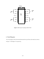
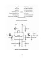
1. Front Panel of TDS 5052B
(a)
CURSORS turn cursors on and off.
Push DEFAULT SETUP to return
settings to factory-default values
INTENSITY
FINE
Push AUTOSET to automatically set up
the vertical, horizontal, and trigger
controls based on selected channels
Select the multipurpose knobs to
adjust parameters selected from
the screen interface. Push a fine
button to toggle between normal
and fine adjustment with the
corresponding multipurpose
knob.
Turn the channel displays on and off.
Vertically scale, position, or change the
input termination.
DEFAULT
SETUP
PRINT
CURSORS
HORIZONTAL
DELAY
FastAcq
TRIGGER
POSITION
ADVANCED
EDGE
SOURCE COUPLING SLOPE
RESOLUTION
FINE
MultiView
Zoom TM
MORE
SAMPLES
SCALE
CH 1
DC
POS
CH 2
AC
NEG
EXT
LINE
HORIZ
TOUCH SCREEN
OFF
Push MultiView Zoom to add a
magnified graticule to the display. Push
HORIZ or VERT to assign the
multipurpose knobs to the horizontal or
vertical scale and position parameters
AUTOSET
RUN/
STOP
SINGLE
NF REJ
ARM
LF REJ
READY
NOISE
REJECT
TRIG’D
MODE
NORM
AUTO
LEVEL
PUSH TO SET 50%
VERT
VERTICAL
POSITION
CH1
POSITION
CH2
1MO
1MO
50O
50O
SCALE
SCALE
(b)
Figure 1.1 (a) Front Panel (b) Control Panel (Tektronix User Manual reference)
1-2
PREPATATION:
a. Calculate the amplitude in dBV of a 1 KHz 2 volt peak-to-peak sine wave.
b. Calculate the peak-to-peak voltage of a –10 dBV 4 KHz sine wave.
EXPERIMENT:
1. TIME DOMAIN DISPLAY
a. Turn on the Oscilloscope and allow a minute for the instrument to boot and stabilize.
Then, press Default Setup to clear settings made by other students. Set the Vertical
scale to 500 mv and the Horizontal scale to 1.0 ms per division.
b. Turn on the Function Generator and connect the output to Channel 1 input of the
oscilloscope.
c. Set the Function Generator for a sine wave output with a frequency of 1 KHz. Adjust
the amplitude to 2 volt peak-to-peak with zero DC offset. The Oscilloscope should
now display 10 cycles of a sine wave. Do not change the Horizontal scale from 1.0
ms through the remainder of this experiment.
Note. Displaying fewer cycles in the time domain display would result in lower
frequency resolution for the frequency domain display. Displaying less than 4 cycles
would result in poor frequency resolution when the frequency domain of the sine wave is
displayed.
2. FREQUENCY DOMAIN DISPLAY
a. Use the mouse to click the Math Button on the Toolbar and select Spectral Setup to
open the Control Window.
b. Under the Create tab, click the Magnitude icon and click Channel 1 as source. Click
Apply.
c. Click the Mag tab. Select dB for the vertical scale factor. Click the Reference Level
Offset, set it to 1000 mV (1 Volt), and click enter. Click Apply.
d. In this experiment, a Gaussian window will be used, which is the default setting.
e. Click OK to close the Control Window.
f. Turn the time domain display off by pressing the CH1 button.
The frequency domain is now displayed. The orange M1 label on the left edge of the
screen indicates the 0dB level. The orange label at the bottom left of the screen now says
Math 1 20.0 dB 25.0KHz. This means each vertical division is 20dBV and each
1-3
horizontal division is 25.0 KHz. Thus, the frequency spectrum is displayed from 0 Hz (on
the left) to 250 KHz on the right.
g. Press the Zoom icon that is located in the Multiview section of the Oscilloscope
Control Panel. Zoom allows detailed analysis of a narrower frequency range.
The waveform in the upper portion of the screen displays the spectrum from 0 to 250
KHz and the lower waveform is the frequency range that is being expanded. A box
appears in the upper waveform to identify the range that is being expanded. Adjust the
upper Multipurpose knob to set the Position to 1% and adjust the lower Multipurpose
knob to set the Factor to 50.
A Zoom Factor of 50 results in a display of
25 KHz 50 = 500 Hz per division.
The white label at the bottom edge of the screen confirms that the Zoom display is set to
20 dB and 500 Hz per division.
Setting the position to 1%, sets the frequency at the center of the screen to
1% of 250 KHz = 2.5 KHz.
Thus, the Zoom is now set to display from 0 Hz to 5 KHz.
The 1 KHz signal should now be visible in the lower waveform.
h. Use the mouse to click the Cursors button on the toolbar. Select Cursors On. Click the
Cursors button again, select Cursor Type, and then click Waveform. Two cursors
appear in the upper waveform, both outside of the zoomed frequency range. Use the
mouse to drag one of the cursors into the zoomed frequency range and position it at
the peak of the 1 KHz signal. Does the amplitude agree with the value that you
calculated in the Preparation?
i. Change the frequency of the Function Generator to 2 KHz. Does this accurately
represent the input signal?
On the Toolbar, click File, click Save As, and save to your floppy disk.
Note. Do not (ever) save to the Local Disk (C:).
j. Change the frequency of the Function Generator to 4 KHz.
Does the frequency domain waveform confirm that the signal is 4 KHz?
k. Decrease the amplitude of the Function Generator output to –10 dBV as measured in
the frequency domain display. Turn the time domain on again by pressing the CH1
button. Turn the Zoom off by pressing the Zoom icon. Read the peak-to-peak voltage
measurement. Does this measurement agree with the value that you calculated in the
Preparation?
1-4
REPORT:
In your report, describe what you have learned in this experiment. Compare your
experimental measurements with the theoretical calculations. Remember to insert the
picture that you saved as part of your report. Write all conclusions.
REFERENCES:
1-5
EXPERIMENT 2
Periodic Signal Spectra
1 Objective
To understand the relationships between time waveforms and frequency spectra.
2 Theory
2.1
Motivation
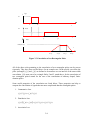
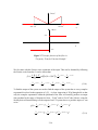
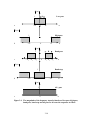
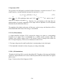
Consider for a moment the special class of systems that are called linear time-invariant
systems. When a signal is applied to this system, the output can be expressed in terms of linear
differential equations with constant coefficients. An example of such a system is shown in
Figure 2.1. The differential equation that describes the input/output relationship in such a
system is given below
d
R
R
v0 (t ) + v0 (t ) = vi (t )
dt
L
L
(2.1)
L
+
+
vi (t )
R
−
vo (t )
−
Figure 2.1 A Simple linear Time-invariant system
For a finite input v i (t ) we expect to solve this differential equation to find the corresponding
output v 0 (t ) . The difficulty involved in this task is that the input has to be a very simple signal.
One way out from this complication is to express the input as a linear combination of simpler to
deal with inputs. The choice of simpler inputs will affect the difficulty which we may encounter
2-1
in solving the problem.
There is an intriguing possibility regarding the simpler input signals. Let us for a moment
assume that we choose as an input a function that repeats itself under the operation of
differentiation. We can show that such a function at the input will yield the same function as an
output multiplied by some algebraic polynomial involving the parameters of the function and
the parameters of the differential equation.
A function that demonstrates this behavior, that is to repeat itself under the operation of
differentiation, is the function e st , where s = σ + jω is a complex number. Since some of the
signals that we are interested in are energy-type signals that may exist for positive or negative
time it is wise to choose σ = 0 . This discussion indicates that if the input signal vi (t ) in
equation (2.1) is of the form e jω t , then we can readily find the output v0 (t) of the system.
Furthermore, if we can express the input signal vi (t ) as a linear combination of complex
exponential signals (of the form e jω t ), we can still find, without difficulty, the output v0 (t ) of
the system (the reason being that the system in (2.1) is linear, and as a result if the input ( v i (t ) )
is a linear combination of complex exponentials ,then the output ( v0 (t ) ) can be expressed as a
linear combination of the outputs of the complex exponentials involved in the input). One
version of the Fourier series expresses an arbitrary signal (like vi (t ) ) as a linear combination of
complex exponentials. This is the first reason that the Fourier series representation of a signal is
so useful.
A close relative of a complex exponential e jω t are the signals cos ω t and sin ω t (remember
Euler’s identity: e jω t = cos ω t + j sin ω t ). Consider now the following set of familiar signals.
f1 (t ) = a sin ω o t
f 2 (t ) = a sin 2ω o t
f 3 (t ) = a sin 3ω o t
.
.
.
.
.
.
(2.2)
f n (t ) = a sin nω o t
In Figure 2.2 we show a plot of f1 (t ) and f 2 (t ) . More generally, we can say that as n increase
2-2
the rate of variation of f n (t ) increases as well.
One way to quantify the above qualitative statements is to take the derivative of f n (t ) with
respect to time. In particular,
d
f (t ) = anω 0 cos nω 0 t
dt
(2.3)
From the above equation we observe that as n increases the maximum rate of variation of
f n (t ) with respect t time increases. We can represent each one of the f n (t ) functions in a little
bit different way than the one used in Figure 2.2. That is, we can represent these functions by
plotting the maximum amplitude of f n (t ) (i.e., a ) versus the angular frequency of the sinusoid
(i.e., nω 0 ). The product of these two values gives you the maximum rate of variation for the
signal under consideration. In Figure 2.3 we are representing the functions f1 (t ) , f 2 (t ) , and
f 3 (t ) following the aforementioned convention. Obviously, larger values for the location of the
plotted amplitudes imply faster varying time signals; also the larger the amplitudes plotted at a
particular location the faster the corresponding signals vary with respect to time.
f1(t)
f2(t)
t
Figure 2.2 Plots of f1(t) and f2(t)
Representation of f1(t),
f2(t),
f3(t)
a
ω0
2ω0
3ω0
ω
Figure 2.3 Reresentation of f1(t), f2(t), f3(t)
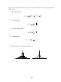
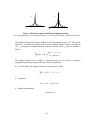
Now consider a simple example of an amplitude-modulated signal.
2-3
f (t ) = A(1 + cos ω m t ) cos ω 0 t ω m << ω 0
(2.4)
In Figure 2.4 we plot the aforementioned signal f(t). As we can see from the figure, the
amplitude varies slowly between 0 and 2A. Its rate of variation is given by ωm, the modulating
frequency; ω0 is referred to as the carrier frequency. The amplitude variations form the
envelope of the complete signal, and represent any information being transmitted. Note that
A(1 + cos ω m t ) cos ω 0 t = A cos ω 0 t +
A
[cos(ω 0 − ω m )t + cos(ω 0 + ω m )t ]
2
(2.5)
The representation of the aforementioned signal, using the new conventions, is illustrated in
Figure 2.5. As we observe from Figure 2.5, larger carrier frequency corresponds to a faster
varying signal; also larger modulating frequency results in a faster varying signal.
f(t)
2A
t
-2A
Figure 2.4 Plot of an amplitude-modulated signal f(t)
A
A/2
ω
ω0 - ωm
ω0
ω0+ωm
Figure 2.5 Representation of the
amplitude-modulated signal f(t)
The previously discussed signals vary in some sinusoidal fashion. They do not carry any
information but we have used them to focus on an alternative representation of the signal, that
conveys to us the information of how fast the signal changes with respect to time. Another
variation of the Fourier series representation of a signal represents the signal as a linear
combination of sines and cosines of appropriate frequencies. As a result, the Fourier series
representation of the signal, which is an extension of the alternative representation of the
2-4
simple signals that we discussed above, gives us an idea of how fast the signal changes with
respect to time. This is the second reason that the Fourier series representation of a signal is so
useful.
2.2 Fourier Series
Let our space S of interest be the set of piecewise continuous real time signals, defined over an
interval (0, T ) . Let us also consider the set of signals
φ10 (t ) =
φ1n (t ) =
1
(2.6)
T
2
φ 2 n (t ) =
(2.7)
cos nω 0 t
T
2
T
sin nω 0 t
n = 1,2, L
(2.8)
where ω 0 = 2π T . The aforementioned signals (see equations (2.6), (2.7) and (2.8)) are
orthonormal. They also constitute a complete set of functions. These two properties allow us to
state that an arbitrary signal in S can be expressed as a linear combination of the signals in
equations (2.6)-(2.8), such that
∞
∞
n=1
n=1
f (t ) = C10φ10 + ∑C1nφ1n + ∑C2nφ2n
(2.9)
and the coefficients in the linear expansion above can be computed through the following
equations:
C10 = ∫ f (t )
T
1
dt
0
T
C1n =
2
T
∫0 f (t ) cos nω 0 tdt
n = 1,2, L
C 2n =
2
T
∫0 f (t ) sin nω 0 tdt
n = 1,2, L
T
T
(2.10)
The above expansion, due to Fourier, is referred to as the Trigonometric Fourier Series
expansion of a signal f (t ) . A more common form for the trigonometric Fourier series
expansion of a signal is given below.
2-5
f (t ) = a0 +
∞
∑
an cosnω0t +
n=1
∞
∑bn sinnω0t
(2.11)
n=1
where
1 T
f (t )dt
T ∫0
2 T
a n = ∫ f (t ) cos nω 0 tdt n = 1,2,L
T 0
2 T
bn = ∫ f (t )sin nω 0 tdt n = 1,2,L
T 0
a0 =
(2.12)
(2.13)
(2.14)
By a simple trigonometric manipulation we get that
f (t ) = a 0 +
∞
∑
n =1
⎧− b ⎫
a n2 + bn2 cos(nω 0 t + θ n ) θ n = arctan ⎨ n ⎬
⎩ an ⎭
(2.15)
The above equation puts f (t ) in the desired form. In other words, we have now expressed f (t )
as a linear combination of sinusoids, and as a result we can represent this signal f (t ) by
plotting the amplitude of each one of its sinusoids at the corresponding angular frequency
location. This will give rise to the amplitude — frequency plot of f (t ) . Observe though that in
equation (2.15) each sinusoid involved in the expansion of f (t ) has a phase associated with it.
Hence, in order to completely describe the signal f (t ) we need to draw another plot that
provides the information of the phase associated with each sinusoid. This plot is denoted as the
phase — frequency plot and it corresponds to a plot of θ n at the location ω n .
It is worth mentioning that the aforementioned expansion of f (t ) in terms of sinusoidal signals
of frequencies that are integer multiples of the frequency ω 0 is often referred to as the
expansion of f (t ) in terms of its harmonic components. The frequency ω 0 is called the
fundamental frequency, or first harmonic, while multiples of the first harmonic frequency are
referred to as the second harmonic, third harmonic, and so on. The corresponding signals in the
expansion are named first harmonic component, second harmonic component, third harmonic
component, and so on. The component a 0 in the above expansion is called the DC component
of the signal f (t ) .
Since we shall frequently be interested in the amplitudes,
a n2 + bn2 ’s, and phases, θ n ’s, of our
signal f (t ) it would be simpler to obtain these directly from f (t ) , rather than by first finding
a n and bn . In order to achieve this, let us consider the functions
2-6
φ n (t ) =
1
T
e jnω 0t
(2.16)
2π
The above set of functions is a complete, orthonormal set. Therefore, any
T
function f (t ) , defined over an interval of length T , can be expanded as a linear combination of
the φ n (t ) ’s. In particular,
where ω 0 =
f (t ) =
∞
∞
∑ C φ (t ) = ∑ C
n = −∞
n
n
n = −∞
1
n
T
e jnω 0t
(2.17)
The coefficients C n in the above expansion are chosen according to the rules specified by the
Orthogonality Theorem. That is,
T
1 jnω 0t
C n = ∫ f (t )
e
dt
(2.18)
0
T
The above equation is denoted as the Exponential Fourier Series expansion of the signal f (t ) .
Actually, in most instances, the exponential Fourier series expansion of a signal is provided by
the following equation:
f (t ) =
∞
∑F e
n=−∞
jnω0t
n
(2.19)
where
Fn =
1 T
f (t )e − jnω0t dt
∫
0
T
(2.20)
Our original goal has now been accomplished, since we can now derive the amplitude —
frequency plot of f (t ) by plotting the magnitude of Fn , with respect to frequency, and we can
also derive the phase — frequency plot of f (t ) by plotting the phase of Fn with respect to
frequency. Note that, in general, the Fn ’s are complex numbers and a complex number Fn , can
be written as the product of its magnitude ( Fn ) times e j∠Fn . One can show that the coefficients
of the exponential Fourier series expansion of f (t ) and the coefficients of the trigonometric
Fourier series expansion of f (t ) are related as follows:
2-7
F0 = a 0
Fn =
1
(a n − jbn ) 1 ≤ n ≤ ∞
2
F− n =
1
(a n + jbn ) 1 ≤ n ≤ ∞
2
(2.21)
The following are some comments:
♦ The exponential Fourier series and the trigonometric Fourier series expansion were
introduced for a signal f (t ) defined over the interval (0, T ) . Actually, the formulas provided
are valid for any signal f (t ) defined over any interval of length T (the starting and the
ending points of they interval are immaterial, as far as the length of the interval is equal to
T ).
♦ We expanded so far a signal f (t ) , defined over an interval of length T , in terms of a linear
combination of sinusoids (Trigonometric Fourier Series expansion), or complex
exponentials (Exponential Fourier Series expansion). It is worth noting, that the
trigonometric or exponential Fourier series expansion of a signal defined over an interval T
is a periodic signal of period T; that is it repeats itself with period T . Hence, if the signal of
interest f (t ) is not periodic the trigonometric or exponential Fourier series expansion of the
signal is only valid for the interval over which the signal is defined.
♦ Due to the periodicity nature of the Fourier series expansion, Fourier series is primarily used
to represent signals of periodic nature. Signals of aperiodic nature can also be represented as
a “sum” of sinusoids or complex exponentials, but this “sum” is in reality an integral and it
is designated by the name Fourier Transform. The Fourier transform of an aperiodic signal
will be introduced later as an extension of the Fourier series of a periodic signal.
2.3
Examples
2.3.1 Example 1
(a) Evaluate the trigonometric Fourier series expansion of a signal f (t ) , which is
depicted in Figure 2.6.
2-8
f(t)
1
cos(t)
-π/2
t
+π/2
Figure 2.6 plot of f(t)=cost for [-π/2, π/2]
and zero elsewhere
The interval of interest is (− π 2,π 2 ) . Hence T = π , and as a result ω 0 = 2π T = 2 . The
trigonometric Fourier series of a signal f (t ) is therefore of the form
∞
∞
n =1
n =1
f (t ) = a 0 + ∑ a n cos 2nt + ∑ bn sin 2nt
a0 =
1 T2
1
f (t )dt =
∫
T
2
−
T
π
an =
2 T2
2 π2
f (t ) cos 2ntdt = ∫ cos t cos 2ntdt =
∫
T
2
−
T
π −π 2
1
π
π 2
∫π
−
cos tdt =
2
π 2
2
bn =
(2.23)
π
∫−π 2 [cos(2n − 1)t + cos(2n + 1)t ]dt =
(2.22)
n +1
(− 1)n ⎤
2 ⎡ (− 1)
+
⎢
⎥
π ⎣ 2n − 1 2n + 1 ⎦
2 T2
2 π2
(
)
f
t
sin
2
ntdt
=
cos t sin 2ntdt = 0
π ∫−π 2
T ∫−T 2
(2.24)
(2.25)
The last equation is a result of the fact that f (t ) is even and sin 2nt is odd. Consequently,
f (t )sin 2nt is odd, and whenever an odd function is integrated over an interval which is
symmetric around zero, the result of the integration is zero. Based on the above equations we
can write:
n +1
(− 1)n+1 ⎤ ⎫⎪ cos 2nt
2 ∞ ⎪⎧ 2 ⎡ (− 1)
f (t ) = + ∑ ⎨ ⎢
(2.26)
+
⎥⎬
π n =1 ⎪⎩π ⎣ 2n − 1 2n + 1 ⎦ ⎪⎭
2-9
Also, if we write out a couple of terms from the above equation we get:
f (t ) =
2
2
2⎡ 2
⎤
t
t
cos 6t + L⎥
+
−
+
cos
4
cos
2
1
⎢
π⎣ 3
35
15
⎦
(2.27)
(b) Find the exponential Fourier series of the signal f (t ) in Figure 2.6.
We can proceed via two different paths. We can either find, directly, the exponential Fourier
series expansion of f (t ) by applying the pertinent formulas, or we can use the trigonometric
Fourier series expansion already derived to generate the exponential Fourier series expansion.
We choose the latter approach, because it is easier. Recall that
f (t ) =
2
π
∞
+ ∑ a n cos 2nt
(2.28)
n =1
where
n +1
n +1
(
2 ⎡ (− 1)
− 1) ⎤
an = ⎢
+
⎥
π ⎣ 2n − 1 2n + 1 ⎦
(2.29)
Due to Euler’s identity we can write
e j 2 nt + e − j 2 nt
cos 2nt =
2
(2.30)
Using Euler’s identity in equation (2.30) we get:
f (t ) =
2
π
∞
a n j 2 nt ∞ a n − j 2 nt
e
+∑ e
n =1 2
n =1 2
+∑
(2.31)
Notice also that the exponential Fourier series expansion of the signal f(t) has the following
form:
2-10
∞
∞
∞
−∞
n =1
n =1
f (t ) = ∑ Fn e j 2 nt = F0 + ∑ Fn e j 2 nt + ∑ F−n e − j 2 nt
(2.32)
Comparing, one by one, the terms of equations (2.31) and (2.32) we deduce the following
identities:
F0 = a0
(2.33)
an
2
(2.34)
Fn =
F− n =
an
2
(2.35)
In particular,
f (t ) =
2
π
+
2 j 2t
2 − j 2t
2 j 4t
2 − j 4t
e +
e
−
e −
e
3π
3π
15π
15π
(2.36)
Based on equations (2.33) through (2.35) we can plot the amplitude - frequency, and the phase
- frequency plots for the signal f (t ) . In the case where the coefficients Fn are real we can
combine these two plots into one plot; this plot is denoted as the line spectrum of f (t ) . The
line spectrum of a signal f (t ) corresponds to the plot of Fn ’s with respect to frequency. The
line spectrum of the signal f (t ) in this example is depicted in Figure 2.7.
2
2/π
3π
2
35π
-3ω0
2
3π
-2ω0
−2
15π
2ω0
-ω0
ω0
−2
15π
2
35π
3ω0
Figure 2.7 Line Spectrum of f(t) of figure 2.6
2-11
ω
(c) Plot the right hand sides (RHS’s) of equations (2.27) and (2.36)
The plot is shown in Figure 2.8. Note that the RHS’s of equation (2.27) and (2.36) is equal to
the signal f (t ) (see Figure 2.6) in the interval (− π 2,π 2 ) . Also the RHS’s of equation (2.27)
and (2.36) are periodic with period π . Hence the plot of Figure 2.8 is produced by reproducing
the plot of Figure 2.7 every π units of time.
cos(t)
ω
-5π/2
-3π/2
-π/2
π/2
3π/2
π5/2
Figure 2.8 Plot of the RHS of equation (2.27)
2.3.2 Example 2
Evaluate the trigonometric Fourier series expansion of the periodic signal f (t ) which is
depicted in Figure 2.9.
f(t)
+1
-π/2
π/4
-π/4
π/2
-1
t
Figure 2.9 plot of f(t)
Let us concentrate on one period of the signal, that is the interval (− π 2,π 2 ) . Knowing that
T = π we conclude that ω 0 = 2π T = 2 . The trigonometric Fourier series of a signal f (t ) is
therefore of the form
∞
∞
n =1
n =1
f (t ) = a 0 + ∑ a n cos 2nt + ∑ bn sin 2nt
2-12
(2.37)
where
a0 =
1
T
an =
2 T2
f (t ) cos 2ntdt
T ∫−T 2
=
2
T 2
−T 2
f (t )dt =
1
π∫
T 2
−T 2
f (t )dt = 0
(2.38)
2
2
∫−π 2 (− cos 2nt )dt + ∫−π 4cos 2ntdt + ∫π 4 (− cos 2nt )dt
−π 4
π
=2
∫
π 4
π
π 2
π
sin (nπ 2)
nπ 2
bn =
(2.39)
2 T2
f (t )sin 2ntdt = 0
T ∫−T 2
(2.40)
The last equation is a result of the fact that f (t ) is even and sin 2nt is odd. Consequently,
f (t )sin 2nt is odd, and whenever an odd function is integrated over an interval which is
symmetric around zero, the result of the integration is zero. Based on the above equations we
can write:
∞
⎧ sin (nπ 2 ) ⎫
(2.41)
f (t ) = ∑ ⎨2
⎬ cos 2nt
nπ 2 ⎭
n =1 ⎩
Also, if we write out a couple of terms from the above equation we get:
f (t ) =
1
1
4⎡
1
⎤
t
t
t
cos14t + L⎥
−
−
+
cos
10
cos
6
cos
2
⎢
π⎣
7
5
3
⎦
(2.42)
3 Power — Parseval’s Relation
3.1 Definitions
The power Pf of a real signal f (t ) is defined as follows:
1
T0 → ∞ T
0
Pf = lim
∫
T /2
−T / 2
f
2
2-13
(t )dt
(2.43)
It is not difficult to show that if the signal f (t ) is periodic with period T , then its power Pf
can be computed as follows:
Pf =
1 T /2
f
T ∫−T / 2
2
(t )dt
(2.44)
Parseval’s relation for periodic signals says that the power content of a periodic signal is the
sum of the power contents of its components in the Fourier series representation of the signal.
In particular, if the exponential Fourier series coefficients of f (t ) is given by the following
equation:
f (t ) =
∞
∑F e
n = −∞
jnω 0t
(2.45)
n
then Parseval’s theorem says that the power Pf of f (t ) is equal to:
2
∞
∑
n = −∞
In the above equation F n
2
(2.46).
Fn
is the magnitude square of the complex number Fn. An alternative
expression of Parseval’s theorem for periodic signals, says that the power of a periodic signal
f(t) is equal to:
1 ∞
2
2
2
a 0 + ∑ a n + bn
(2.47)
2 n =1
(
)
where the a n ’s and bn ’s in the above equation are the trigonometric Fourier series coefficients
of the periodic signal f (t ) .
Besides being an alternative way of calculating the power of a periodic signal, Parseval’s
relation allows us to calculate the amount of power of a periodic signal that is allocated to each
one of its harmonic components.
3.2 Example 3
(a)Find the power contained in the first harmonic of the periodic signal f (t ) of Example 1
2-14
From the trigonometric Fourier series expansion of f (t ) (see equation (2.27)) we observe that
the first harmonic of f (t ) is equal to:
4
cos(2t )
3π
(2.48)
It is not difficult to show that the amount of power contained in the first harmonic is equal to
[4 (3π )]2 as Parseval’s relation predicts.
2
(b) Find the power contained in the first and second harmonics of the periodic signal f (t )
of Example 1
From the trigonometric Fourier series expansion of f (t ) (see equation (2.27), we observe that
the first and second harmonic of f (t ) is equal to:
4
4
(2.49)
cos(4t )
cos(2t ) +
15π
3π
It is not difficult to show that the amount of power contained in the first two harmonics is equal
2
2
[
4 (3π )] [4 (15π )]
+
as Parseval’s relation predicts.
to
2
2
(c) Find the power contained in the DC component of the periodic signal f (t ) of Example 1
From the trigonometric Fourier series expansion of f (t ) , (see equation (2.27)) we observe that
the DC component of f (t ) is equal to 2 π . Hence the amount of power contained in the DC
component is equal to (2 π ) .
2
2-15
4 Pre-lab Questions
1. Find both the trigonometric and the exponential Fourier series expansion of the signal
f(t) in Figure 2.9. Plot the amplitude frequency for the signal. Identify the first three
harmonics and their amplitude. Find the power content from the time domain
representation of the signal and from the first three harmonics of the Fourier series
expansion, and make appropriate remarks.
2. What is the difference between an energy signal and a power signal? Give two
examples of each.
5 Implementation
In this lab you will be introduced to the relationship between pulse shapes and their spectra.
There are some important concepts to recognize when performing the experiment, such as:
1. When a pulse becomes narrower in the time domain its energy becomes more spread out in
frequency.
2. The envelope of the spectrum of a periodic signal is the Fourier transform of the pulse shape.
To illustrate the first concept given above, consider the Fourier Transform of a rectangular
pulse shown in Figure 2.11. It can be found from the frequency domain graph (Figure 2.11) that
90% of the energy is concentrated within the main lobe in frequency. As the pulse width is
decreased in time, or T decreases, the width of the main lobe in the frequency domain spreads,
thus spreading out the energy of the signal.
To illustrate the second concept, recall that when two signals are convolved in the time domain,
their transforms are multiplied in the frequency domain.
Any periodic signal can be represented mathematically described as the basic pulse shape
convolved with a time sequence of pulses. Thus the spectrum of the periodic signal can be
derived as shown in Figure 2.12.
6 Procedure
EQUIPMENT:
TDS5052B Oscilloscope
Function Generator
You should bring a floppy disk to store your waveforms.
2-16
6.1. Sine Wave
In this section you will observe when the signal frequency of a sine wave is shifted, the spectral
line will also shift in frequency.
a. Turn on the Oscilloscope and allow a minute for the instrument to boot and stabilize. Then,
press Default Setup to clear settings made by other students. Turn on the Function
Generator and connect the output to Channel 1 input of the oscilloscope. Adjust the
function generator for the oscilloscope to display 10 cycles of a 1 KHz, 0.5 volt peak sine
wave with zero DC offset. Do not change the Horizontal scale setting of the oscilloscope
during the remainder of the experiment. Do not change the amplitude or DC offset settings
of the Function Generator during the remainder of the experiment.
Note. Be sure the Function Generator Duty Cycle knob is set to Cal.
b. Use the mouse to click the Math Button on the Toolbar and select Spectral Setup to open
the Control Window. Under the Create tab, click the Magnitude icon and click Channel 1
as source. Click Apply.
c. Click the Mag tab and select Linear for the vertical scale factor. Click the Scale, set the
vertical scale to 100 mv rms per division, and click Enter. Click Apply. Click OK to close
the Control Window.
d. Press the Zoom icon. Set the Zoom Position to 2.5% and the Zoom Factor to 20.
e. Determine the amplitude and frequency displayed for the spectrum of the sine wave. Save
the waveform to include in your report.
f. Change the Function Generator frequency to 5 KHz. Determine the amplitude and
frequency displayed and save the waveform to include in your report.
6.2. Square and Rectangular Waves
A rectangular wave contains many sine wave harmonic frequencies. When the reciprocal of
the duty cycle (either the positive or negative duty cycle) is a whole number, the harmonics
corresponding to multiples of that whole number will be missing. For example, if the duty
cycle is 50%, then 1/0.5 = 2. Thus, the 2nd, 4th, 6th, etc. harmonics will be missing, i.e. zero.
A rectangular wave with a 50% duty cycle is a square wave. For the square wave, the
magnitude of the harmonic will be inversely proportional to the harmonic’s number. For
example, if the magnitude of the 1st harmonic is A, then the magnitude of the 3rd harmonic is
A/3, the 5th harmonic’s magnitude is A/5, etc.
2-17
a. Change the Function Generator frequency to 1 KHz and function to square wave.
b. Determine the amplitude and frequency displayed for the 1st, 3rd, 5th, and 7th harmonics in
the spectrum of the square wave. Identify the zeros of the spectrum envelope (i.e. the
frequency locations at which harmonic amplitudes are zero). Save the waveform to include
in your report.
c. The duty cycle of a pulse is measured as illustrated in Figure 2-10. The TDS5052B
Oscilloscope can automatically measure duty cycle. Click Measure on the Toolbar and
click Measurement Setup. Under Source, click Channel 1. Click the Time tab and click +
Duty Cyc. Click Freq. Click Close. Duty cycle and frequency should now be displayed on
the right edge of the screen.
d. Change the duty cycle of the 1 KHz rectangular wave to 10%. Hint: Pull the Duty Cycle
Knob to invert the waveform for duty cycles of less than 50%. Changing the duty cycle also
changes the frequency, so you will also need to readjust the frequency until you attain both
1 KHz and 10% duty cycle. Notice that a DC component appears in the frequency domain
display. The DC component of the signal from the Function Generator is negative.
However, the DC component observed in the frequency domain display is positive because
the magnitude is the rms value, which is always positive. Determine the amplitude and
frequency of the 1st, 2nd, 3rd, 4th, and 5th harmonics. Determine the location of zeros.
Save the waveform.
e. Change the duty cycle of the 1 KHz rectangular wave to 25%. Determine the amplitude and
frequency of the 1st, 3rd, 5th, 6th, and 7th harmonics. Determine the location of zeros.
Save the waveform.
f. Change the duty cycle of the 1 KHz square wave to 90%. Determine the amplitude and
frequency of the 1st, 2nd, 3rd, 4th, and 5th harmonics. Determine the location of zeros.
Save the waveform.
tw
tp
duty cycle = (tw/tp) * 100%
Figure 2.10 Duty cycle of a square
wave signal
2-18
6.3. Triangular Wave
The triangular wave, like the square wave, only contains odd numbered harmonics. The
magnitude of the harmonics is inversely proportional to the square of the harmonic’s number.
For example, if the 1st harmonic’s magnitude is A, then the 3rd harmonic’s magnitude will be
A/9, the 5th harmonic’s magnitude will be A/25, etc.
a. Set the Function Generator Duty Cycle knob to Cal and switch the function to triangular
wave. Set the frequency to 1 KHz. Determine the amplitude and frequency of the 1st, 3rd,
and 5rd harmonics.
b. Determine the location of zeros. Save the waveform.
7 Calculations and Questions
1. Compare the waveforms you obtained for rectangular waves on the basis of harmonic
location, zero location, and peak spectrum amplitude (i.e. first harmonic level). Explain the
results on the basis of the pulse width and signal frequency.
2. Use your data to show that the spectrum of a triangular wave is equal to the spectrum of a
square wave squared.
3. The spectrum of the square wave should decay proportional to 1 ω (where ω = 2πf ). The
spectrum of the triangular wave should decay proportional to (1 ω ) . Verify this using your
measurements.
2
2-19
Time Domain
A rect(t/ T)
A
-T/2
0 T/2
F(A rect(t/T) = ATSin(πfT)/( πfT)
ATSin(πfT)/( πfT)
AT
AT
-2/T
-1/T
0
-1/T
-2/T
MAIN LOBE
Figure 2.10 Rectangular Function and its
frequency representation (Fourier transform)
2-20
Time Domain
Frequency Domain
ATsin(πfT1)/( πf T1)
A rect(t/ T1)
A T1
A
0 T1/2
-T1/2
-1/ T1
0
-1/ T1
+1/ T2
-T2
0
-4
T2
T2
-3
T2
-2
T2
-1
T2
1
T2
0
2
T2
AT1
T2
-T2+ T1 -T1 0
2 2
T1 T2- T1
2
2
T2+ T1
2
F(f)
f(t)
Figure 2.11 Mathematic representation of a periodic signal in the
time and frequency domain
2-21
3 4
T2 T2
EXPERIMENT 3
Low Pass Filter
1 Objective
To observe some applications of low-pass filters and to become more familiar with working in
the frequency domain.
2 Theory
2.1 Systems
A communication system consists of three major components: the transmitter, the channel and
the receiver. The transmitter and the receiver are comprised of a cascade of black boxes that
accept input signals, produce output signals, and they are referred to as systems. This section is
devoted to understanding what a system does, and clarifying the various types of systems used
in the transmitter and receiver for a communication system.
Definition: A system is a rule for producing an output signal (g (t )) due to an input signal ( f (t )) .
. , then
If we denote the rule as T []
g (t ) = T [ f (t )]
(3.1)
An electric circuit with some voltage source as the input and some current branch as the output
is an example of a system.
Note that for two systems in cascade, the output of the first system forms the input to the
second system, thus forming a new overall system. If the rule of the first system is T1 and the
rule of the second system is T2 , then the output of the overall system due to an input
f (t ) applied to the first system is equal to g (t ) , such
g (t ) = T2 [T1 [ f (t )]]
(3.2)
There are a variety of classifications of systems that owe their name to their properties. In this
section we will focus only in the classification of systems into the linear versus nonlinear
categories and the time-invariant versus time-variant categories.
If a system is linear then the principle of superposition applies. The output of a system with rule
T []
. that satisfies the principle of superposition exhibits the following property:
T [a1 f1 (t ) + a 2 f 2 (t )] = a1T [ f1 (t )] + a 2T [ f 2 (t )]
3-1
(3.3)
Where a1 and a 2 are arbitrary constants. A system is nonlinear if it is not linear. A linear system
(friendly system) is usually described by a linear differential equation of the following form:
a n (t )g n (t ) + a n −1 (t )g n −1 (t ) + K a1 (t )g 1 (t ) + a0 (t )g 0 (t ) = f (t )
(3.4)
Where g (t ) designates the output of the system, while f (t ) designates the input of the system.
In the above equation g k (t ) denotes the k − th time derivative of the function g (t ) .
Virtually every system that you consider in your circuit classes (e.g., first order
R − C , R − L circuit, second order R − L − C circuits) is an example of linear systems. Any
circuit that has components, whose v − i curve is nonlinear (e.g., a diode) is likely to be a
nonlinear system.
Another useful classification of systems is into the categories of Time-Invariant versus TimeVarying systems. A system is time-invariant if a time-shift in the input results in a
corresponding time-shift in the output. Quantitatively, a system is time-invariant if
g (t − t 0 ) = T [ f (t − t 0 )]
(3.5)
For any t 0 and any pair of f (t ) and g (t ) , where f (t ) denotes an input to the system and g (t ) ,
denotes its corresponding output. A system is time-varying if it is not time-invariant.
As we emphasized before, a linear system is described by a linear differential equation of the
form shown in equation (3.4). If in the differential equation (3.4) the coefficients a k (0 ≤ k ≤ n )
are constants and not functions of time, then we are dealing with a linear time-invariant system.
Otherwise, we are dealing with a linear time-varying system. Examples of linear time-varying
systems from your circuit classes were circuits consisting of R, L and C components and
involving one or more switches that were ON or OFF at special instances.
2.2 The Convolution Integral
The convolution integral appears quite often in situations where we deal with a linear time
invariant system (LTI). If this system is excited by an input f (t ) and the impulse response of
the system is h(t ) , then the output g (t ) of the system is equal to the convolution of f (t ) and
h(t ) , as illustrated below
g (t ) = f (t ) * h(t ) =
∞
∫
−∞
f (t − τ )h(τ )dτ =
∞
∫ h(t − τ ) f (τ )dτ
(3.6)
−∞
Note that the impulse response of a linear, time-invariant system is defined to be the output of
the system due to an input that is equal to an impulse function, located at t = 0 . In this manual
we are going to demonstrate the convolution of two rectangular pulses.
3-2
2.3 Convolution Examples
Consider two rectangular pulses, f 1 and f 2 , depicted in Figure 3.1. We are going to find the
convolution of these two rectangular pulses. We designate the convolution by f 3 (t ) . That is
f 3 (t ) = f1 (t ) * f 2 (t ) =
∞
∫ f (t − τ ) f (τ )dτ
1
(3.7)
2
−∞
f1(t)
0
1
2
3
4
1
2
3
4
5
6
f2(t)
0
5
6
Figure 3.1 two rectangular pulses to be convolved
We want to compute the convolution of f1 (t ) and f 2 (t ) . It seems that we have to compute the
convolution integral for infinitely many instances of time t (see equation (3.7)). A more
careful observation though allows us to distinguish the distinct t -range over which the
convolution integral needs to be evaluated. One way of finding the distinct t -range is by
remembering that equation (3.7) tells us that we need to slide the rectangle f1 with respect to
the stationary rectangle f 2 and identify the product of these two pulses over the common
interval of overlap. It is not difficult to show that the sliding rectangle f 1 (actually f1 (t − τ ) ) is
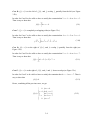
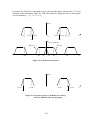
nonzero over the τ -interval (t − 2, t − 1) . We now distinguish five cases:
Case A: f1 (t − τ ) is to the left of f 2 (τ ) , and f1 and f 2 do not overlap (see Figure 3.2a).
In order for Case A to be valid we have to satisfy the constraint that t − 1 < 3 or t < 4 . Then is
easy to show that
f 3 (t ) = 0
(3.8)
3-3
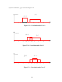
Case B: f1 (t − τ ) is to the left of f 2 (τ ) , and f1 overlap f 2 partially from the left (see Figure
3.2b).
In order for Case B to be valid we have to satisfy the constraint that 3 < t − 1 < 4 or 4 < t < 5 .
Then is easy to show that
f 3 (t ) =
t −1
∫ dτ = t − 4
(3.9)
3
Case C: f1 (t − τ ) is completely overlapping with (see Figure 3.2c).
In order for Case C to be valid we have to satisfy the constraint that 4 < t − 1 < 5 or 5 < t < 6 .
Then is easy to show that
f 3 (t ) =
t −1
∫ dτ = (t − 1) − (t − 2) = 1
(3.10)
t −2
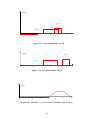
Case D: f1 (t − τ ) is to the right of f 2 (τ ) , and f 1 overlap f 2 partially from the right (see
Figure 3.2d).
In order for Case D to be valid we have to satisfy the constraint that 5 < t − 1 < 6 or 6 < t < 7 .
Then is easy to show that
f 3 (t ) =
5
∫ dτ = 5 − (t − 2) = 7 − t
(3.11)
t −2
Case E: f1 (t − τ ) is to the right of f 2 (τ ) , and f1 and f 2 do not overlap (see Figure 3.2e).
In order for Case E to be valid we have to satisfy the constraint that 6 < t − 1 or t > 7 . Then is
easy to show that
f 3 (t ) = 0
(3.12)
Hence, combining all the previous cases, we get
⎧ 0 for t < 4
⎪ t − 4 for 4 < t < 5
⎪⎪
f 3 (t ) = ⎨1
for 5 < t < 6
⎪7 − t for 6 < t < 7
⎪
⎪⎩ 0 for t > 7
3-4
(3.13)
A plot of the function f 3 (t ) is shown in Figure 3.2f
Case A
1
0
f 2 (τ )
f1 (t − τ )
t-2
2
t-1
3
4
5
6
τ
Figure 3.2 a : Convolution under Case A
Case B
1
0
f1 (t − τ )
2
t-2
3
f 2 (τ )
t-1
4
5
6
τ
6
τ
Figure 3.2 b : Convolution under Case B
Case C
0
f1 (t − τ )
f 2 (τ )
1
2
3
t-2
4
t-1
5
Figure 3.2 c : Convolution under Case C
3-5
Case D
f1 (t − τ )
f 2 (τ )
1
0
2
3
4
t-2
5
t-1
τ
6
Figure 3.2 d : Convolution under Case D
Case E
f 1 (t − τ )
f 2 (τ )
0
1
2
3
4
5
t-2
6 t-1
τ
Figure 3.2 e : Convolution under Case E
f 3 (t )
t
0
1
2
3
4
5
6
7
Figure 3.2 f Function f 3 (t ) (The result of convolution of f1(t) and f2(t))
3-6
Based on our previous computations we can state certain rules pertaining to the convolution of
two rectangles. These rules can be proven following the technique laid out in the previous
example. These rules can be used to find the convolution of two rectangle pulses, without
actually having to compute the convolution.
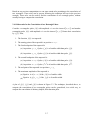
2.4 Golden rules for the Convolution of two Rectangle Pulses.
Consider a rectangular pulse f1 (t ) with amplitude A1 over the interval [x1 , x 2 ] , and another
rectangular pulse f 2 (t ) with amplitude A2 over the interval [ y1 , y 2 ] . Denote their convolution
by f 3 (t ) . Then,
1. The function f 3 (t ) is a trapezoid.
2. The starting point of the trapezoid is at position x1 + y1 .
3. The first breakpoint of the trapezoid is
(a) At position x1 + y 2 if pulse f 2 (t ) is of smaller width than pulse f1 (t ) .
(b) At position x 2 + y1 if pulse f1 (t ) is of smaller width than pulse f 2 (t ) .
4. The second breakpoint of the trapezoid is
(a) At position x 2 + y1 if pulse f 2 (t ) is of smaller width than pulse f1 (t ) .
(b) At position x1 + y 2 if pulse f1 (t ) is of smaller width than pulse f 2 (t ) .
5. The end point of the trapezoid is at position x 2 + y 2
6. The maximum amplitude of the trapezoid is
(a) Equal to A1 A2 ( x 2 − x1 ) if the f1 (t ) is of smaller width.
(b) Equal to A1 A2 ( y 2 − y1 ) if the f 2 (t ) is of smaller width.
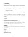
A plot of f1 (t ) , f 2 (t ) and f 3 (t ) is shown in Figure 3.3. The technique, described above, to
compute the convolution of two rectangular pulses can be generalized, in a trivial way, to
compute the convolution of arbitrary shaped, finite-duration pulse.
3-7
f1(t)
A1
x1
A2
x2
t
F2(t)
y1
F3(t)
t
y2
A1A2(x2-x1)
t
x1+y1
x1+y2
x2+y1
x2+y2
Figure 3.3 Convolution of two Rectangular Pulse
All of the above rules pertaining to the convolution of two rectangular pulses can be proven
rigorously. They have been verified above for an example case. In the special case where the
pulse (rectangle) f1 (t ) and f 2 (t ) are defined to be nonzero over an interval of the same width
convolution f 3 (t ) turns out to be a triangle. Rules 2 and 5, stated above, for the convolution of
two rectangular pulsed extend for the case of the convolution of arbitrary shaped, finiteduration pulses.
Some useful properties of the convolution are listed below. These properties can help us
compute the convolution of signals that are more complicated than the rectangular pulses.
1. Commutative Law.
f1 (t ) * f 2 (t ) = f 2 (t ) * f1 (t )
2. Distributive Law
f1 (t ) * [ f 2 (t ) + f 3 (t )] = f 1 (t ) * f 2 (t ) + f 1 (t ) * f 3 (t )
3. Associative Law
3-8
f1 (t ) * [ f 2 (t ) * f 3 (t )] = [ f 1 (t ) * f 2 (t )]* f 3 (t )
4. Linearity Law
[α f1 (t )]* f1 (t ) = α [ f1 (t ) * f1 (t )]
Where α in the above equation is a constant.
2.5 Impulse Function
The impulse function showed up in the discussion of the convolution integral and linear timeinvariant system. We said then, that the convolution integral allows us to compute the output of
a linear time-invariant system if we know the system’s impulse response. The impulse response
of a system is defined to be the response of the system due to an input that is the impulse
function located at t = 0 .
The impulse or delta function is a mathematical model for representing physical phenomena
that take place in a very small time duration, so small that it is beyond the resolution of the
measuring instrument involved, and for all practical purposes, their duration can be assumed to
be equal to zero. Examples of such phenomena are a hammer blow, a very narrow voltage or
current pulse, etc. In the precise mathematical sense, the impulse signal, denoted by
δ (t )
is not a function (signal), it is a distribution or a generalized function. A distribution is defined
in terms of its effect on another function (usually called “test function”) under the integral sign.
The impulse distribution (or signal) can be defined by its effect on the “test function” φ (t ) ,
which is assumed to be continuous at the origin, by the following relation:
b
⎧φ (0 ) : a < 0 < b ⎫
⎬
otherwise ⎭
∫ φ (t )δ (t )dt = ⎨⎩ 0 :
a
This property is called the sifting property of the impulse signal. In other words, the effect of
the impulse signal on the “test function” φ (t ) under the integral sign is to extract or sift its
value at the origin. As it is seen, δ (t ) is defined in terms of its action on φ (t ) and not in terms of
its value for different values of t .
One way to visualize the above definition of the impulse function is to think of the impulse
function as a function determined via a limiting operation applied on a sequence of well-known
3-9
signals. The defining sequence of signals is not unique and many sequences of signals can be
used, such as
1. Rectangular Pulse:
1⎡ ⎛ τ ⎞
⎛ τ ⎞⎤
δ (t ) = lim ⎢U ⎜ t + ⎟ − U ⎜ t − ⎟⎥
2⎠
⎝ 2 ⎠⎦
τ →0 τ ⎣ ⎝
2. Triangular Pulse:
1⎡
t⎤
δ (t ) = lim ⎢1 − ⎥
τ⎦
τ →0 τ ⎣
3. Two-sided exponential
δ (t ) = lim e − 2 t
τ →0 τ
1
τ
4. Gaussian Pulse
δ (t
) = lim 1
τ
τ → 0
e
−π
( t τ )2
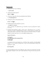
The above functions are depicted in Figure 3.4
1/τ
1/τ
−τ/2
τ/2
t
−τ
0
τ
0
(a)
(b)
3-10
t
1/τ
1/τ
t
(c)
t
(d)
Figure 3.4 Function sequence definition of impulse function:
(a) rectangular pulses; (b) triangular pulses; (c) two-sided exponentials; (d)Gaussian pulses.
The impulse function that we have defined so far was positioned at time t = 0 . In a similar
fashion we can define the shifted version of the impulse function. Hence, the function
δ (t − t 0 ) designates an impulse function located at position (time) t 0 , and it is defined as
follows:
⎧φ (t 0 ) : a < t 0 < b
(
)
(
)
t
t
t
dt
φ
δ
−
=
⎨
0
∫
b
⎩ 0 : otherwise
a
The impulse function has a number of properties that are very useful in analytical
manipulations involving impulse functions: They are listed below:
♦ Area (Strength): The impulse function δ (t ) has unit area. That is
b
∫ δ (t − t )dt = 1
0
a < t0 < b
a
♦ Amplitude:
δ (t − t 0 ) = 0
for all t ≠ t 0
♦ Graphic representation
See Figure 3.5
3-11
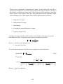
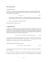
δ(t)
t
Figure 3.5 Function δ(t)
♦ Symmetry
δ (t ) = δ (− t )
♦ Time Scaling
δ (at ) =
1
δ (t )
a
♦ Multiplication by a time function
f (t )δ (t − t 0 ) = f (t 0 )δ (t − t 0 )
♦ Relation to the Unit Step Function:
The unit step function is the function defined by
⎧1 : t > t 0
U (t − t 0 ) = ⎨
⎩0 : t < t 0
It is not difficult to see that
t
∫ δ (τ − t )dτ = U (t − t )
0
−∞
And that
3-12
0
δ (τ − t 0 ) =
d
U (t − t 0 )
dt
♦ Convolution Integral.
f (t ) * δ (t ) = f (t )
f (t ) * δ (t − t 0 ) = f (t − t 0 )
Similar to the definition of δ (t ) we can define δ (1) (t ) , δ ( 2 ) (t ) , K , δ (n ) (t ) , the generalized
derivatives of δ (t ) by the following equation:
b
∫δ
a
(n )
⎧
dn
⎪(− 1)n n φ (t ) t =0 : a < 0 < b
(t )φ (t )dt = ⎨
dt
⎪⎩
0 : otherwise
We can generalize this result to
b
∫δ
a
(n )
⎧
dn
⎪(− 1)n n φ (t ) t =t0 : a < t 0 < b
(t − t 0 )φ (t )dt = ⎨
dt
⎪⎩
0 : otherwise
For even values of n , δ '(n ) (t ) is even, and for odd values of n , δ '(n ) (t ) is odd.
2.6 The Frequency Transfer Function
Consider a linear-time invariant system, which is described by the following differential
equation.
M
∑ am
m =0
d m g (t ) K
d k f (t )
b
=
∑
k
dt m
dt k
k =0
(3.14)
In the above equation, f (t ) represents the input to the system, and g (t ) represents the output of
d 0 f (t )
denote 0-th derivative of f (t ) ; same convention holds for
the system. The expression
dt 0
g (t ) .
3-13
Assume for a moment that the input f (t ) to the above system is equal to e jωt . Then, we prove
that the output of the system is equal to g (t ) = H (w)e jωt with
K
H (ω ) =
∑ b ( jω )
k
k
k =0
M
∑ a ( jω )
m =0
(3.15)
m
m
In actuality we are contending that if the input to the system is a complex exponential function
( e jωt ) the output of the system will be the same exponential function times a constant ( H (ω ) )
which depends on the input parameters ( ω ) and the system parameters (the a ’s and b ’s) when
we are referring to H (ω ) as being a constant we mean that it is independent of time. The
constant H (ω ) is called the transfer function of the system. When the Fourier transform is
introduced it will be easy to prove that the transfer function of a system is the Fourier transform
of the impulse response of the system. We have already stated that the impulse response of a
linear time invariant system describes the system completely. We can make a similar statement
about the transfer function of a linear, time-invariant system. That is, if we know the transfer
function of a LTI system we can compute the output of this system due to an arbitrary input.
Since, we are still operating in the context of Fourier series expansions, and since Fourier series
expansions are most appropriate for periodic signals, consider for a moment a periodic input
f (t ) applied to the system of equation (3.14). Obviously, f (t ) has a Fourier series expansion
whose form is given below.
f (t ) =
∞
∑F
n = −∞
n
e jnω 0t
(3.16)
It is not difficult to demonstrate that in this case the output g (t ) of our system will be equal to
g (t ) =
∞
∑ H (nω )F
n = −∞
0
n
e jnω 0t
(3.17)
Equation (3.17) validates out claim that the frequency transfer function of a linear time
invariant system is sufficient to describe the output of the system due to an arbitrary input (at
least for the case of an input which is periodic). After the Fourier transform is introduced we
will be able to extend this result to aperiodic inputs as well. Looking at equation (3.17) more
carefully we can make a number of observations:
Observation 1: If the input to a linear time-invariant system is periodic with period T0 =
2π
ω0
,
then the output of this system is periodic with the same period.
Observation 2: Only the frequency components that are present in the input of a LTI system
can be present in the output of the LTI system. This means that a LTI system cannot introduce
3-14
new frequency components other than those present in the input. In other words all systems
capable of introducing new frequency are either nonlinear systems or time-varying systems or
both.
2.7 Frequency transfer Function Example
Let f (t ) be a signal as shown in Figure 3.6. This signal is passed through a system (filter) with
transfer function as shown in Figure 3.7. Determine the output g (t ) of the filter.
f(t)
−T0
−T0/2
T0/2
T0
Figure 3.6 input signal f(t) to the filter in
“Frequency Transfer Function Example”
3-15
t
⏐H (ω)⏐
−12π ×105
12π ×105
ω
∠H (ω)
π/2
ω
−π/2
Figure 3.7 Transfer function of the filter in
“Frequency Transfer Function Example”
We first start with the Fourier series expansion of the input. This can be obtained by following
the Fourier series formulas. It can be shown that
n
5
5
4 ∞ (− 1)
2
2
f (t ) = ∑
cos 2π (2n + 1)10 5 t = e j 2π 10 t + e − j 2π 10 t
π n = 0 2n + 1
π
π
[
−
]
2 j 6π 105 t 2 − j 6π 105 t
2 j10π 105 t
2 − j10π 105 t
e
−
e
+
e
+
e
+K
3π
3π
5π
5π
(3.18)
To find the output of the system we need to find the output of the system due to every complex
exponential involved in the expansion of f (t ) . A closer inspection of H (ω ) though tells us that
only the complex exponential within the passband of the filter will actually produce an output
(the passband is the range of frequencies from − 12π 10 5 rads to 12π 10 5 rads.) Hence, using the
already derived formula that gives the output of an LTI system due to a periodic input, we can
write:
5
5
5
2
2
2
g (t ) = e j (2π 10 t +π 2 ) + e − j (2π 10 t +π 2 ) − e j (6π 10 t +π 2 )
π
−
2
π
π
e j (6π 10
5
t +π 2
π
) + 2 e j (10π 10 t +π 2 ) 2 e − j (10π 10 t +π 2 )
π
π
5
3-16
5
(3.19)
2.8 Filters
Filtering has a commonly accepted meaning of separation - something is retained and
something is rejected. In electrical engineering, we filter signals usually frequencies. A signal
may contain single or multiple frequencies. We reject frequency components of a signal by
designing a filter that provides attenuation over a specific band of frequencies, and we retain
components of a signal through the absence of attenuation or perhaps even gain over a
specified band of frequencies. Gain may be defined as how much the input is amplified at the
output.
Filters are classified according to the function they have to perform. Over the frequency
range we define pass band and stop band. Ideally pass band is defined as the range of
frequencies where gain is 1 and attenuation is 0, and stop band is defined, as the range of
frequencies where the gain is 0 and the attenuation is infinite.
Filters can be mainly classified as low pass, high pass, band pass and band stop filters.
A low pass filter can be characterized by the property that the pass band extends from
frequency ω = 0 to ω = ±ω c , where ω c is known to be the cutoff frequency. (See Figure
3.8(a))
A high pass filter is the complement of a low pass filter. Here the previous frequency range
ω = 0 to ω = ω c is the stop band and the frequency range from ω = ω c to positive infinity and
ω = −ω c to negative infinity is the pass band. (See Figure 3.8(b))
A band pass filter is defined as the one where frequencies from ω1 to ω 2 are passed while all
other frequencies are stopped. (See Figure 3.8(c))
3-17
H (ω )
1
B
− ωc
a
Low-pass
ωc
0
ω
H (ω )
1
b
High-pass
− ωc
ωc
0
ω
H (ω )
B
Band-pass
ω1 ω 0 ω 2
ω
1
c
− ω 2 − ω 0 − ω1
0
H (ω )
Band-stop
1
d
− ω2
− ω1
0
ω1
− ω2
ω
H (ω )
1
e
All - pass
ω
0
Figure 3.8 The magnitude of the frequency transfer function of low-pass, high-pass,
band-pass, band-stop and all-pass. In all cases the responses are ideal
3-18
A band stop filter is the compliment of the band pass filter. Frequencies from ω1 to ω2 are
stopped here and all other frequencies are passed. (See Figure 3.8(d))
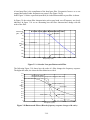
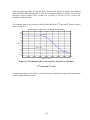
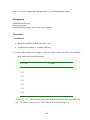
In the Figure 3.9 below a practical (non-ideal) 6th order Butterworth low-pass filter is shown.
In Figure 3.9 the various filter characteristics such as pass band, cut-off frequency are clearly
indicated. In figure 3.10 we are illustrating how the filter characteristics change with the
order of the filter.
5
6 order Low-pass Butterworth Filter
Passband
0
gain
3 dB point
-5
-10
-15
Gain
-20
dB
Passband
-25
-30
-35
-40
0
Cut-off Frequency
500
1000
1500
2000 2500 3000
Frequency (Hz)
3500
4000
4500
5000
Figure 3.9 6-th order Low-pass Butterworth Filter
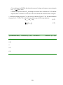
The following Figure 3.10 shows how the order of a filter changes the frequency response.
The higher the order, the closer the filter behaviors as ideal.
1.2
1.1
1
Butterworth Filter:
How the frequency response changes with order
0.9
0.8
Cutoff frequency
0.7
Gain
0.6
2nd order
0.5
0.4
0.3
24th order
6th order
0.2
Figure
0.13.10 Butterworth Filters (How the frequency response changes with order)
0
0
1000 Filters (How
2000 the frequency
3000 response4000
Figure 3.10
Butterworth
changes with 5000
order)
Frequency (Hz)
Figure 3.10 Butterworth Filters (How the frequency response changes with order)
3-19
Filters are key components in communication systems. An ideal filter will only allow a
specified set of frequencies to pass from input to output with equal gain. However, no filter is
ideal, and as a result there are many types of filters, that are used in modeling an ideal filter
closely in one or more aspects. Filters have many applications besides separating a signal
form surrounding noise or other signals. Some of these applications are listed below.
1. Integration of a signal
2. Differentiation of a signal
3. Pulse shaping
4. Correcting for spectral distortion of a signal
5. Sample and hold circuits
Two Butterworth low pass filters (LPF’s) will be used in this lab: a first order and a fourthorder Butterworth filter. The general transfer function of a Butterworth LPF is:
H (ω ) =
2
A
(1 + ω ω 0 )2 n
Where ω 0 = the filter cutoff frequency and
n = the order of the filter
The actual transfer functions of the filters that are going to be used in this lab are:
1st order LPF: H (s ) =
1
1 + RCS
(3.20)
4th order LPF:
H L (s ) =
⎛
⎜ (RCS )4
⎜
⎝
⎛
R ⎞⎛ R ⎞
⎜⎜1 + 2 ⎟⎟⎜⎜1 + 4 ⎟⎟
R1 ⎠⎝
R3 ⎠
⎝
⎞
⎞⎞
⎛ ⎛ R + R2 ⎞
⎛ ⎛ R + R2 ⎞
⎟⎟ RCS + 1⎟(RCS )2 + ⎜ 3 − ⎜⎜ 1
⎟⎟ RCS + 1⎟ ⎟
+ ⎜⎜ 3 − ⎜⎜ 1
⎟
⎟⎟
⎜
⎠
⎠⎠
⎝ ⎝ R1 ⎠
⎝ ⎝ R1 ⎠
Where ω 0 = 1 RC for both filters
3-20
Two applications for low pass filters will be illustrated in this lab:
1. A LPF used as an integrator
2. A LPF used as a first harmonic isolator (square-to-sine conversion).
2.8.1 Integrator
The Laplace representation of integration is 1 s (where s = jω ). A first order low pass filter
can approximate an integrator when ω >> ω 0 {then V0 Vin = 1 (s ω 0 )}
For an n th order low-pass filter, the transfer function will approximate n integrators in series at
V (s )
1
ω >> ω 0 , or 0
=
Vin (s ) (s ω 0 )n
For simplicity, in this lab a first order LPF will be used to perform a single integration on a
signal.
2.8.2 Square-to-sine-Converter
Any periodic signal can be expressed as an infinite sum of orthogonal sinusoids. For
orthogonality, each sinusoid (or “harmonic”) must have a different frequency, and frequency
must be an integer multiple of the frequency of the periodic signal.
For example, if the frequency of a square wave is f s , then the n th harmonic will have a
frequency of n * f s (where n is any integer from one to infinity). You will see that some of
these harmonics will have zero or negative amplitude.
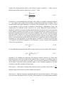
The harmonics of a square wave of frequency f s are shown in Figure 3.11 (Not to scale); the
DC component of the square wave is assumed to be equal to zero.
3 fs
f
s
2 fs
4 fs
5 fs
f
Figure 3.11 The harm onics of a square wave form of frequency
3-21
fs
If the square wave excites the input of the low pass filter such that the first harmonic is in the
pass band of the filter transfer function and the remaining harmonic are outside of the pass
band, then the output of the low pass filter will be a single-tone signal (sinusoid).
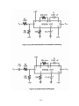
3. Simulation
We will use Matlab simulation to see the response of our filter circuits. For simulation you will
need the transfer functions of both filter circuits shown in figure 3.15 and 3.16. The transfer
functions were given earlier in this manual (See equation 3.20 and 3.21.)
In both filters R = 1.6kΩ and C = 0.01μF . For the second filter R1 = 10kΩ , R2 = 12kΩ ,
R3 = 10kΩ , R4 = 1.5kΩ and C = 0.01μF . With the above values for resistors and capacitors
the transfer functions will have the following form (notice that the coefficients are in
descending order of s ).
H1 =
H2 =
1
1 + (RC ) s
2.2 × 1.5
( RC ) s + 2.65( RC ) s + 3.48( RC ) 2 s 2 + 2.65 RCs + 1
4
4
3 3
Construct a frequency array as following.
w=[0:100:100000];
Construct the coefficient vectors as follows:
b=[coefficients of numerator separated by comma];
a=[ coefficients of denominator separated by comma];
Use the MATLAB ‘freqs’ function to generate frequency response of the corresponding filter.
Plot the frequency response of both filters in a single graph using the following a Matlab
function.
Note: The freqs function is not available in all MatLab installations. It is installed in all EE
Labs at UCF.
3-22
Apply the above procedure for both the filters. Note that the frequency response you obtained
from the MATLAB simulation that is gain versus angular frequency in radian. You can also
plot gain versus frequency (Hz). In that case you have to use the f=w/2π vector as the
parameter in plot function.
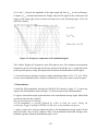
The simulated gain versus frequency (Hz) plot for both filters (2nd order and 6th order) is shown
below as Figure 3.12.
Frequency response of Butterwoth Filter
3
2.8
2.6
6th order
2.4
2.2
2
Gain
1.8
1.6
1.4
1.2
1
2nd order
0.8
0.6
0.4
0.2
0
0
2000
4000
6000
8000
10000
Frequency (Hz)
12000
14000
16000
Figure3.12 The simulated gain versus frequency (Hz) plot for both filters
(2nd order and 4th order)
Compare the response of two filters. After the hardware experiment compare the experimental
results with the simulated results.
3-23
4. Prelab Questions:
1. Calculate the Trigonometric Fourier Series of a square wave with the parameters shown
(assume it is periodic with periodic T):
+ A
0
−T 2
T 2
−A
Figure 3.13 a pe riodic square wave with pe riod T
You may find it easier to add a DC level of A volts. This will only change your spectrum at
f=0, where you can subtract the DC back out.
2. Assuming an ideal filter with a cutoff frequency of ω c ( ω c = 2π T ), show graphically, in
the frequency domain, why the first harmonic of the square wave should be the only
harmonic at the output.
3. Suppose you have an input signal with frequency components from 0 to 2 KHz. Is it
possible to design a filter, which will produce an output with frequency components 4 to 6
KHz? Why or why not?
4. What is the difference between dB/octave and dB/decade?
5. Component
In this lab, we will use OpAmp module TL084 which is shown in figure 3.14
3-24
TL084
Amp
#1
Out 1
14 + Out
- In 2
13 - In
+ In 3
+ Vcc 4
Amp
#2
Top
View
Amp
#4
12 + In
11 -VEE
+ In 5
10 + In
- In 6
9 - In
Out 7
8 Out
Amp
#3
Figure 3.14 Pin layout of OpAmp module TL084
6. Circuit Diagrams:
The circuit diagram of the first order and fourth order low-pass filter used in this lab are shown
in Figure 3.15 and Figure 3.16 respectively.
3-25
7. Procedure
7.1 Filters
a)
Build the lowpass filter shown in Figure 3.15.
b) Using either the oscilloscope, AC voltmeter or spectrum analyzer, determine the
cutoff frequency of the filter (-3 dB from the passband), the passband gain, and the
filter rate of rolloff (in dB/decade or dB/octave).
c)
Build the lowpass filter shown in Figure 3.16 and repeat step (b). Keep both circuit
built for the remainder of the lab.
R
vin
vout
C
Figure 3.15 First order low-pass filter
C
C
C
C
vi
R
R
R
+
R
+
vo
-
R1
R2
R3
Figure 3.16 4th-order low-pass filter
3-26
R4
R = 1.6 K
C = 0.01µF
R1 = 10 K
R2 = 12 K
R3 = 10 K
R4 = 1.5 K
Calculating Filter Parameters
The following procedures will help you understand how to measure filter parameters on the
scope or AC voltmeter:
7.2 Cutoff frequency
a)
From the function generator, obtain a .2 volt, low frequency (10 or 100 Hz range)
sine wave. It is important to use a sine wave because there is only one harmonic in a
sinusoid, and you only want to test the transfer function at one point in frequency at
time. Connect the function generator output to the filter input.
b) Connect the filter output to the oscilloscope (See Figure 3.18) or AC voltmeter input
(See Figure 3.17).
c)
Vary the input frequency by a factor of 2 or 3 either way and make sure the output
level doesn’t vary significantly. If it doesn’t, then your input frequency. is within the
pass band. When you know you are within the pass band, measure the output voltage
level (or dB level). This will be your reference level.
d) Vary the input frequency until the output level drops 3 dB below the reference level.
On the AC voltmeter this can be read directly. On the oscilloscope, -3 dB is
equivalent to the voltage level reduced by a factor of .707 (or, at –3 dB point, Vout(3dB) = .707 (Vout(ref)). Note this frequency. This is your cutoff frequency.
7.3 Passband gain
a)
Using the function generator, generate a .2 volt sine wave at a frequency that you
know to be within the filter passband. Connect the function generator output to the
filter input.
b) Measure the output voltage ( V0 ). The filter passband gain is equal to
V0 Vin = V0 .2 (See Figure 3.18).
7.4 Rate of rolloff
a)
Use the function generator to generate a sinusoid at a frequency that is higher than
the cutoff frequency of the filter (maybe by a factor of 2 or so). Record the input
amplitude ( Vin ) or measure in dB on the AC voltmeter (you may want to use an
input amplitude of 1 volt or more since the output will be attenuated).
3-27
b)
Connect the function generator output to the filter input. Measure the filter output
in volts ( Vo ) or dB. Calculate Vo Vin and convert to dB ( 20 log(Vo Vin ) or subtract
the input dB level from the output dB level. This will give you the attenuation, in
dB, at your selected frequency.
c)
Repeat steps 1 and 2 with a frequency that is a factor of 2 higher than the first
frequency used. If you take the difference between the two calculated values of
attenuation, in dB, this will be your rate of rolloff in dB/octave. If you want to
convert, (N) dB/octave corresponds to ( (N) * (20/6)) dB/decade.
7.5 Square Wave Spectrum
a) Use the function generator to generate a square wave of 0.2 volts amplitude and 1kHz
frequency, and connect its output to Cannel 1 input of the oscilloscope.
b) Set up the display of the Oscilloscope in order to see 10cycles of the square wave.
c) Generate a spectrum analysis waveform in dBV with a reference voltage offset of
1Volt.
• From the Math Menu, select Spectral Set Up. Create the Magnitude spectra by
clicking in the Magnitude and channel-1 icons respectively.
• Click Mag Tab and click the dB icon for vertical scale factor.
• At the reference menu:
Set the Level to 0dB (This will place the M1 label at the upper side of the screen.)
Set the Level offset to 1 volt (Reference voltage for dBV scale.)
Set the scale to 10 dB (10dB per division in the vertical scale.)
d) Clear the time domain waveform turning OFF Channel 1.
e) Using Zoom option from the Multiview section. Adjust the Multipurpose Knobs to
Factor of 10 (narrows the width of the zoom window to 12.5KHz) and to a Position
of 5% (place the left side limit of the zoom window to 0dB.) You may need to press
the HORIZ bottom to re-adjust your measurements.
You should see the first six nonzero harmonics of the square wave displayed. Record the
amplitude (in dBV) and frequency of each harmonic. You can use the Cursor in cursor
window type.
3-28
7.6 Integrator
a)
Generate a square wave of amplitude 5V (peak) and frequency= 10 × ω c (ten times
the cutoff frequency). Apply this signal to the input of the filter from Figure 3.15
(the first order filter)
b)
Sketch the output of the filter from the oscilloscope, recording signal peak-to-peak
amplitude.
7.7 Square-to-Sine conversion (First Harmonic Isolation)
a)
Obtain a .2 volt peak square wave with frequency f = .75 × f c from the function
generator.
b)
Apply the signal from (a) to the input of the filter in Figure 3.15. Sketch the output
signal in both the time and frequency domains, scaling axes.
c)
Repeat b) with the filter in Figure 3.16
PWR 1M
100K
10K
1K
DUTY
100
10
TTL
1
DC OFFSET AMPLITUDE
FUNCTION GENERATOR
AC MILIVOLTMETER
OUTPUT
FREQUENCY
R.M.S. VOLTS
DECIBELS
dB mV
0 300
INPUT
in
DUT
out
1
0
-10 100
3 +10
-20 30
10 +20
-30 10
30 +30
-40 3
100 +40
-50 1
300 +50
Figure 3.17 Measuring cutoff frequency using AC Voltmeter
3-29
V dB POWER
ON
PW 1M 100
R
K
10
K
1K
DUTY
10
0
TTL
10
1
DC
AMPLITU
OFFSET
DE
OUTPUT
FREQUEN
CY
in
DUT
ou
t
Figure 3.18 Measuring passband using the oscilloscope.
8 Calculations and Questions
1.Convert the values you measured from the spectrum analyzer in dBV to volts and
compare to your Fourier Series Coefficients from (1). Recall that the measured
amplitudes are RMS amplitudes, so the values must be multiplied by the square root of 2.
2. Compare your results from section IV parts (b) and (c) on the basis of filter gain and
filter roll off rate that you measured.
3. Using the waveform shown in question (1), Integrate (in time) to show that the integral
of a square wave is a triangular wave. What peak amplitude do you calculate? Recall that
you have to solve an indefinite integral to get an answer in functional form.
4. When the first harmonic of the input signal is well beyond the filter cutoff frequency, a
first order low pass filter cutoff frequency, a first order low pass filter approximates an
integrator (shown in ‘Integrator‘ section of lab introduction). Show that this transfer
function, when applied to your square wave, will closely predict the output amplitude you
measured. Note that this transfer function can be reduced to a constant multiplied by the
integral of the input signal. Also note that your DC level may vary from that calculated,
because the DC level will depend on at what point on the square wave the integration
began.
3-30
Laboratory 4
Amplitude Modulation
1 Objective
To understand the amplitude modulation.
2 Theory
2.1 From Fourier series to the Fourier Integral
The Fourier series is a means for expanding a periodic signal in terms of complex exponentials.
This expansion considerably decreases the complexity of the description of the signal, and
simultaneously, this expansion is particularly useful when we analyze LTI systems.
We can extend the idea of the Fourier series representation from periodic signals to the case of
nonperiodic signals. That is the expansion of a nonperiodic signal in terms of complex
exponentials is still possible. However, the resulting spectrum is not discrete any more. In other
words, the spectrum of nonperiodic signals covers a continuous range of frequencies. To be
able to demonstrate our point, consider for a moment the periodic signal shown in Figure 4.1.
fT(t)
1
τ
-T
τ
-T/2
-τ/2
0
τ/2
T/2
T
t
Figure 4.1 A periodic signal fT(t)
We call this periodic signal f T (t ) to remind ourselves that we are dealing with a periodic signal
of period T . We can write:
−T
T
⎧⎪
f (t ) :
<t<
(4.1)
f T (t ) = ⎨
2
2
⎪⎩ 0 : otherwise
4-1
where f (t ) is equal to the periodic signal f T (t ) over the interval (− T 2,T 2 ) and zero
otherwise. Obviously, f T (t ) has a Fourier series expansion, such that
f T (t ) =
∞
∑F e
n = −∞
jnω 0t
(4.2)
n
With
Fn =
1 T2
1 T2
f T (t )e − jnω 0t dt = ∫ f (t )e − jnω 0t dt
∫
T −T 2
T −T 2
(4.3)
Also, since f T (t ) and f (t ) are equal over the interval (− T 2,T 2 ) we can write that
f (t ) =
∞
∑ Fn e jnω0t =
n = −∞
where
∞
1
∑ T F (ω )e ω
j
n
n = −∞
nt
(4.4)
F (ω n ) = TFn
(4.5)
ω n = nω 0
(4.6)
and
Let us now define
Δω = ω n +1 − ω n = ω 0 =
2π
T
(4.7)
Then, from equation (4.7) we get
f (t ) =
Δω
F (ω n )e jω nt
n = −∞ 2π
∞
∑
(4.8)
Let now T go to ∞ , or equivalently, Δω goes to zero. It is easy to see that the equation (4.8)
becomes:
1 ∞
(4.9)
f (t ) =
F (ω )e jωt dω
∫
−
∞
2π
Also, it is not difficult to show that
∞
F (ω ) = ∫ f (t )e − jωt dt
−∞
(4.10)
Equations (4.9) and (4.10) are referred to as the Fourier Transform pair, that allows us to
transform the aperiodic time signal f (t ) into the frequency signal F (ω ) , and vice versa. Based
4-2
on the aforementioned discussion we can now formally introduce the Fourier transform
theorem.
2.2 Fourier Transform Theorem
If the signal f (t ) , satisfies certain conditions known as the Dirichlet conditions, namely,
1. f (t ) is absolutely integrable on the real line, that is,
∫
∞
f (t ) dt < ∞
−∞
2. The number of maxima and minima of f (t ) in any finite interval of the real line is finite.
3. The number of discontinuities of f (t ) in any finite interval of the real line is finite.
then, the Fourier transform (FT) of f (t ) , defined by
F (ω ) = ∫
∞
−∞
f (t ) e − jωt dt
(4.11)
exists and the original signal can be obtained from its FT by following the rule
f ± (t ) =
1
2π
∫
∞
−∞
F (ω ) e jωt dω
(4.12)
where
if f (t ) is continuous at t
⎧ f (t ) :
⎪
f ± (t ) = ⎨ f (t + ) + f (t − )
: if f (t )is continuous at t
⎪⎩
2
(4.13)
Observation 1:
The Fourier transform, F(ω) of a signal, f(t), is, in general, a complex function. Its magnitude
F (ω ) and phase represent the amplitude and phase of various frequency components of f (t ) .
4-3
Observation 2:
If the independent variable in the FT of a signal is chosen to be the frequency f instead of the
angular frequency ω we have the following Fourier transform pair:
∞
X ( f ) = ∫ x(t )e − j 2π ft < ∞
(4.14)
−∞
and
∞
x(t ) = ∫ X ( f )e j 2π ft df
(4.15)
−∞
2.3 Fourier Series to Fourier Transform Example
Let f T0 (t ) be a periodic signal depicted in Figure 4.2.
f T0 (t)
1
τ
- T0
τ
- T0 /2
τ/2
0
-τ/2
T0/2
T0
t
Figure 4.2 A periodic signal fT0 (t)
The Fourier series expansion of this signal, of period T0 , is given by the following equation.
f T0 (t ) =
∞
∑F e
n = −∞
jnω 0t
n
(4.16)
f (t ) e − jnω 0t dt
(4.17)
where
Fn =
and
1
T0
∫
T0 2
−T0 2
4-4
ω0 =
2π
T0
(4.18)
We can compute Fn ’s as follows:
Fn =
=
1
T0
∫
T0 2
−T0 2
f (t ) e − jn 2πt / T0 dt =
[
1 T0
e − jnπτ
T0 − jn 2π
T0
1
T0
− e + jnπτ
T0
τ
∫ τ f (t ) e
2
− jn 2πt / T0
− 2
dt
nπτ T ) τ
] = sinn(πτ
⋅
T
T
0
0
(4.19)
0
The line spectrum of the signal f T0 (t ) is shown in Figure 4.3 for τ T0 = k −1 . Note that the
separation of two consecutive lines in the line spectrum of f (t ) is equal to 2π T0 . Hence, as
T0 gets larger and larger (i.e., as f T0 (t ) becomes less and less periodic-looking) the line
spectrum of f T0 (t ) becomes denser and denser. Also, note that the envelope of line spectrum of
f T0 (t ) is the Fourier transform (within a constant of proportionality) of the aperiodic pulse of
width τ , centered at t = 0 . It can be shown that most of the power of f T0 (t ) is located within
the frequency interval [− 2π τ , − 2π τ ] . This indicates to us that as we make the signal faster in
the time domain (by decreasing the duration τ of the pulses) the frequency content of the
signal gets expanded in the frequency domain. This statement is a manifestation of what is
called in communication theory the "time-bandwidth" product. It can be shown that the timebandwidth" product is constant; that is if we expand the signal in the time domain, we shrink
the frequency content of the signal in the frequency domain, and vice versa.
_τ sinc(xτ/2)
T0*
-2kπ
T0
= -2π
τ
2π
T0
4π
T0
x
2kπ = 2π
T0
τ
Figure 4.3. The line spectrum of the signal f T0 (t)
4-5
2.4. Fourier Transform Properties
The Fourier transform of an aperiodic signal is as useful as the Fourier series of a periodic
signal. As a reminder, the Fourier series of a periodic signal allows us to compute the output of
a LTI system due to a periodic input, without having to compute the convolution. Furthermore,
the Fourier series of a periodic signal provides us with information pertaining to the frequency
content of the signal. Similarly, the Fourier transform of a signal allows to compute the output
of a LTI system due to an input, without having to compute the convolution. Also, the Fourier
transform of the signal contains information about the frequency content of the signal.
Equations (4.11) and (4.12) or equations (4.14) and (4.15) are rarely used for the computation
of the Fourier transform of signals. Normally, the Fourier transform of a signal is computed by
utilizing Fourier transforms of well known signals (see Table 4.1) and Fourier Transform
Properties (see Table 4.2).
The Linearity Property says that the Fourier Transform (FT) is a linear operation and if We
know the FT of two signals We can easily compute the FT of any linear combination of these
two signals. The Scaling Property says that by contracting (expanding) the signal in the time
domain (through multiplication with an appropriate time constant) results in the expansion
(contraction) of the FT of the signal (through multiplication with the inverse of the constant);
this is another ramification of the "time-bandwidth" product principle. Note that contraction
(expansion) of the signal in the time domain corresponds to making the signal faster (slower).
The Delay Property illustrates something that you might have suspected all along. Delaying a
signal in the time domain does not change the frequency content of the signal. The frequency
content of the signal is determined by looking at the magnitude of the FT of the signal. The
delay property reiterates that a time shift will produce a phase shift in the FT of the signal but it
will leave the magnitude of the FT unaltered. The Convolution Property assures us that we do
not need to perform convolution to produce the output of a LTI system due to an arbitrary
input; simply multiplying the FT of the input and the FT of the impulse response of the system
allows us to compute the FT of the output of the system. The Time Differentiation and Time
Integration properties demonstrate that making the signal faster/slower (differentiate/integrate)
in the time domain results in an expanded/contracted frequency spectrum (FT). The Duality
Property provides us with a new FT pair, every time a FT pair is computed. In particular, if F is
the FT of f, the duality property says that F would a FT that is proportional to the mirror image
of f with respect to the ω = 0 axis. Finally, the Amplitude Modulation property tells us that we
can shift the frequency content of a signal at an arbitrary frequency by multiplying the signal
with a sinusoid. AM systems are based on this property of the FT.
2.5 Introduction to Communication Systems
The primary function of most communication systems is to transmit information from point A
to point B. Consider, for example, the situation where we have to transmit human voice from
point A to point B and the channel between points A and B is the air. The human voice at point
A is first converted, via a microphone, to an electrical signal. Then, we have to transform this
4-6
electrical signal into an electromagnetic wave and send it to destination B. The way to achieve
that is by using an antenna. Knowing though that the maximum frequency content of a voice
signal is around 15 KHz we come to the conclusion that the antenna required must be many
miles long! A reasonable size antenna could adapt the signal to the channel only if the signal's
lower frequency is higher than 800 KHz. Hence, in our case, where a voice signal needs to be
transmitted using a reasonable-size antenna it suffices to raise the frequency content of the
voice signal to the vicinity of 800 KHz. To accomplish the aforementioned goal we ought to
multiply the voice signal with a sinusoidal signal. The result of this multiplication is to latch
our f (t ) (the voice signal) on the amplitude of the sinusoid, or to modulate the original
amplitude of the sinusoid with f (t ) . This procedure gives rise to a class of systems that are
called amplitude modulation systems.
We distinguish four major classes of amplitude modulation systems: Double Sideband
Suppressed Carrier Systems (DSB-SC), Single Sideband Suppressed Carrier Systems (SSBSC), Double Sideband Large Carrier Systems (DSB- LC), and Vestigial Sideband Suppressed
Carrier Systems (VSB-SC).
2.6 Double Sideband Suppressed Carrier System (DSB-SC)
Basically double sideband suppressed carrier (DSB-SC) modulation arises by multiplying the
information signal f (t ) and the carrier wave c(t ) , as follows:
m(t ) = c (t ). f (t ) = Ac cos(ω c t ) f (t )
(4.20)
Consequently, the modulated signal m(t ) undergoes a phase reversal whenever the formation
signal f (t ) crosses zero as indicated in Figure 4.4. The envelope of a DSB-SC modulated
signal is therefore different from the information signal.
4-7
Figure 4.4 The information signal f(t) and modulated signal m(t)
The Fourier transform of m(t ) can easily be determined from the Fourier transform properties
of Table 4.2. That is,
1
(4.21)
M (ω ) = Ac [F (ω − ω c ) + F (ω + ω c )]
2
For the case when the baseband signal f (t ) is bandlimited to the interval [− ω m , ω m ] , as in
Figure 4.5(a), we thus -find that the spectrum of m(t ) is as illustrated in Figure 4.5(b). Except
for a change in scale factor, the modulation process simply translates the spectrum of the
baseband signal by ± ω c . Note that the transmission bandwidth required by DSB-SC
modulation is equal to 2ω m , where ( ω m stands for the maximum frequency content of the
signal f (t ) .
4-8
F(ω)
F(0)
-ωm
ωm
0
ω
M(ω)
½AcF(0)
-ωc
0
ωc
-2ωm
ω
2ωm
Figure 4.5 (a) Spectrum of baseband signal. (b) Spectrum of DSB-SC modulated wave
The baseband signal f (t ) can be uniquely recovered from a DSB-SC wave m(t ) by first
multiplying m(t ) with a locally generated sinusoidal wave and then low pass filtering the
product, as in Figure 4.6. It is assumed that the local oscillator signal is exactly coherent or
synchronized, in both frequency and phase, with the carrier wave c(t ) , used in the product
modulator to generate f (t ) . This method of demodulation is known as coherent detection or
synchronous demodulation.
m(t)
Product
modulator
Low –pass
filter
e(t)
o(t)
'
A c cos(ωct+ф)
Local
oscillator
Figure 4.6 Coherent detection of DSB-SC modulated wave.
4-9
It is instructive to derive coherent detection as a special case of the more general demodulation
process using a local oscillator signal of the same frequency but arbitrary phase difference φ ,
measured with respect to the carrier wave c(t ) . Thus, denoting the local oscillator signal by
A ' c cos(ω c t + φ ) and using equation (4.1) for the DSB-SC wave, we find that the product
modulator output in Figure 4.7 is
e(t ) = A ' c cos(ω c t + φ )m(t )
= Ac A ' c cos(ω c t ) cos(ω c t + φ ) f (t )
=
1
1
Ac A ' c cos(2ω c t + φ ) f (t ) + Ac A ' c cos φf (t )
2
2
(4.22)
E(ω)
½*AcAc’F(0)cosφ
¼ *AcAc’F(0)
-2ωc
2ωm
2ωc
2ωm
2ωm
ω
Figure 4.7 Illustrating the spectrum of a product modulator
out put with a DSB-SC modulated wave as input
The first term in equation (4.22) represents the DSB-SC modulated signal with a carrier
frequency of 2ω c , whereas the second term is proportional to the baseband signal f (t ) . This is
further illustrated by the spectrum (Fourier Transform) E (ω ) shown in Figure 4.7, where it is
assumed that the baseband signal f (t ) is limited to the interval [− ω m , ω m ] . It is therefore
apparent that the first term in equation (4.22) is removed by the low-pass filter in Figure 4.6,
provided that the cut-off frequency of this filter is greater than ω m but less than 2ω c − ω m . This
is satisfied by choosing ω c > ω m . At the filter output we then obtain a signal given by
1
o(t ) = Ac A ' c cos(φ ) f (t )
(4.23)
2
The demodulated signal o(t ) is therefore proportional to f (t ) when the phase error φ is a
constant. The amplitude of this demodulated signal is maximum when φ = 0 , and is minimum
4-10
(zero) when φ = ±
π
. The zero demodulated signal, which occurs for φ = ±
π
, represents the
2
2
quadrature null effect of t.he coherent detector. Thus the phase error φ in the local oscillator
causes the detector output to be attenuated by a factor equal to cos φ . As long as the phase
error φ is a constant, the detector output provides an undistorted version of the original
baseband signal f (t ) . In practice, however, we usually find that the phase error φ varies
randomly with time, due to random variations in the communications channel. The result is that
at the detector output, the multiplying factor cos φ also varies randomly with time, which is
obviously undesirable. Therefore, provision must be made in the system to maintain the local
oscillator in the receiver in perfect synchronism, in both frequency and phase, with the carrier
wave used to generate the DSB-SC modulated signal in the transmitter.
2.7 Quadrature-Carrier Multiplexing
The quadrature null effect of the coherent detector may also be put to good use in the
construction of the so-called quadrature-carrier multiplexing or quadrature-amplitude
modulation (QAM). This scheme enables two DSB-SC modulated waves (resulting from the
application of two physically independent information signals) to occupy the same channel
bandwidth, and yet it allows for the separation of two information signals at the receiver output.
It is therefore a bandwidth conservation scheme.
4-11
Message
signal
f1(t)
Product
modulator
+
Multiplexed
signal
m(t)
Σ
+
Accos(ωct)
-900
phase-shifter
Acsin(ωct)
Message
signal
f2(t)
Product
modulator
(a)
Product
modulator
Ac’cos(ωct)
m(t)
Multiplexed
signal
½* Ac Ac’f1(t)
Low-pass
filter
-900
phase-shifter
Ac’sin(ωct)
½* Ac Ac’f2(t)
Product
modulator
Low-pass
filter
(b)
Figure 4.8 Quadrature-carrier multiplexing system.
(a) Transmitter. (b) Receiver.
4-12
A block diagram of the quadrature-carrier multiplexing system is shown in Figure 4.8. The
transmitter part of the system shown in Figure 4.8(a), involves the use of two separate product
modulators that are supplied with two carrier waves of the same frequency but differing in
phase by -90 degrees. The transmitted signal m(t ) consists of the sum of these two product
modulator outputs, as shown by
m(t ) = Ac f1 (t ) cos(ω c t ) + Ac f 2 (t )sin (ω c t )
(4.24)
where f1 (t ) and f 2 (t ) denote the two different information signals applied to the product
modulators. Thus m(t ) occupies a channel bandwidth of 2ω m centered at the carrier frequency
ω c , where ω m is the maximum frequency content of the signals f1 (t ) and f 2 (t ) .
The receiver part of the system is shown in Figure 4.8(b) .The multiplexed signal m(t ) is
applied simultaneously to two separate coherent detectors that are supplied with two local
carriers of the same- frequency but differing in phase by -90 degrees. The output of the top
1
1
detector is Ac A ' c f 1 (t ) , whereas the output of the bottom detector is Ac A ' c f 2 (t ) . For the
2
2
system to operate satisfactorily it is important to maintain the correct phase and frequency
relationships between the local oscillators used in the transmitter and receiver parts of the
system.
To maintain this synchronization, we may use a Costas receiver. Another commonly used
method is to send a pilot signal outside the passband of the modulated signal. In the latter
method, the pilot signal typically consists of a low-power sinusoidal tone whose frequency and
phase are related to the carrier wave c(t ) ; at the receiver the pilot signal is extracted by means
of a suitably tuned circuit and then translated to the correct frequency for use in the coherent
detector.
2.8 The Single Sideband Suppressed Carrier System (SSB-SC)
The DSB-SC system discussed so far sends the signal m(t ) over the channel with Fourier
transform shown in Figure 4.9. One important observation regarding the Fourier transform of
m(t ) is that is consists of two sidebands, the upper sideband and the lower sideband. There is
no need to send both sidebands over the channel, since the FT of the information signal f (t )
can be constructed from either the upper or the lower sideband. The single sideband suppressed
carrier (SSB-SC), that we intend to discuss in the following, takes advantage of the above
observation by sending only one of the sidebands over the channel.
4-13
Figure 4.9 An amplitude modulation suppressed-carrier transmission
Hence, the SSB-SC system differs from the DSB-SC system because just before the modulated
wave m(t ) is ready to head-off for the channel, one of the sidebands is chopped off. The block
diagram of an SSB-SC system is shown in Figure 4.10. Furthermore, the sequence of Fourier
transform plots shown in Figure 4.11 (upper sideband) demonstrate that the system works. The
only problem with the block diagram of the system shown in Figure 4.10 is that it requires the
utilization of a "perfect filter" that eliminates completely the frequencies a little bit below ω c
and passes without distortion the frequencies a little bit above ω c (we are referring only to the
positive frequencies of the upper sideband signal). To relax the requirement for such a "perfect"
filter we will consider another way of generating the upper sideband version of the signal m(t ) .
4-14
f(t)
Χ
m(t)
Sideband
Remover
m’(t)
Channel
coswct
m’(t)
Amplifier
e(t)
Χ
Low –pass
filter
coswct
Figure 4.10 Block diagram of a SSB-SC system
4-15
o(t)
F(ω)
1
1/2
ωm
-ωm
ω
M(ω)
1/2
1/4
-ωc
ωc
ω
ωc
ω
M’(ω)
1/2
1/4
-ωc
E(ω)
1/4
1/4
1/8
-2ωc
1/8
ωm
-ωm
ω
2ωc
O(ω)
-ωm
ωm
Figure 4.11: FT’s at various stage of the SSB-SC system of Figure 4.10
4-16
ω
For the sake of simplicity consider first the case where the information signal is sinusoidal (i.e.,
f (t ) = cos(ω m t ) . Then, the Fourier transform of m(t ) = cos(ω m t ) cos(ω c t ) is given in Figure
4.12. From Figure 4.12, it is easy to identify the upper sideband of m(t ) in the frequency
domain; also, the time-domain representation of this upper sideband is readily defined as
follows:
1
m + (t ) = cos(ω c + ω m )t
(4.25)
2
or
1
1
m+ (t ) = cos(ω c t ) cos(ω m t ) − sin (ω c t )sin (ω m t )
(4.26)
2
2
M(ω)
upper sideband
-ωc-ωm
-ωc
-ωc+ωm
ωc-ωm
ωc
ωc+ωm
ω
lower sideband
Figure 4.12 Fourier transform of m(t) = cos(ωm+ωc)t
In Figure 4.13 we depict a way of constructing the upper sideband signal of equation (4.26)
without having to resort to the design of perfect filters. In Figure 4.13 there is a system
designated by a block with the -90 notation inside it. We know what this block does to an input
signal that is sinusoidal; it shifts the phase of the sinusoidal signal by -90 degrees. We want to
be able to characterize this block in the frequency domain. To do so let us identify the Fourier
transforms of an input signal to this block, equal to cos(ω m t ) and the output signal produced by
this block, equal to cos(ω m t − 90 ) = sin (ω m t ) . Obviously,
FT [sin (ω m t )] = − jπδ (ω − ω m ) + jπδ (ω + ω m )
(4.27)
FT [cos(ω m t )] = πδ (ω − ω m ) + πδ (ω + ω m )
Based on the above equations it is straightforward to derive the result that
4-17
(4.28)
FT [sin (ω m t )] = − jsignum(ω )FT [cos(ω m t )]
(4.29)
where the function signum(ω ) is equal to 1 when ω > 0 and equal to -1 when ω < 0 . Equation
(4.29) tells us that the transfer function of the block designated by the notation -90 is equal to
− jsignum(ω ) . Now we are ready to generalize the construction of an upper sideband signal
using the block diagram of Figure 4.13 for the case where the information signal f (t ) is of
arbitrary nature (i.e., not necessarily sinusoidal). In Figure 4.14, we provide a block diagram for
the construction of the upper sideband signal of a modulated wave m(t ) when the information
signal f (t ) is arbitrary. Comparing Figures 4.13 and 4.14 we see that they are identical, where
in both figures the block designated by the notation -90 corresponds to a system with transfer
function equal to − jsignum(ω ) .
In Figure 4.15 we show, in a pictorial fashion, why the block diagram of Figure 4.14 works.
What is worth noting is that the output of a -90 degree shift system is called the Hilbert
transform of the input. Furthermore, if we designate by f (t ) the input to a -90 degree shift
∧
system the output (Hilbert transform) of this system is designated by f (t ) . Finally, it is easy to
show that
1
(4.30)
f (t ) = f (t ) ∗
πt
4-18
cosωct
cosωmt
+
-900
m+(t)= cos(ωc+ωm) t
-
sinωct
sinωmt
Figure 4.13 Block diagram of a system that generates the
upper sideband of m(t) ( f(t)=cosωmt , c(t) = cosωct )
½*F(ω+ωc)+½*F(ω-ωc)
cosωct
+
f(t)
-900
m+(t)
-
sinωct
-900
∧
∧
∧
f(t)
F(ω) = - j sgn(ω)F(ω)
∧
j/2* F(ω+ωc) - j/2* F(ω-ωc)
= ½*sgn(ω+ωc)F(ω+ωc)
- ½* sgn(ω-ωc)F(ω-ωc)
Figure 4.14 Block diagram of a system that generates the upper sideband of m(t)
4-19
F(ω)
1
ωm
-ωm
ω
½*F(ω+ωc)+ ½*F(ω-ωc)
1/2
-ωc-ωm
-ωc
ωc-ωm
-ωc+ωm
ωc
ωc+ωm
ω
-½*sgn(ω+ωc) F(ω+ωc)- ½*sgn(ω-ωc) F(ω-ωc)
1/2
ωc-ωm
-ωc+ωm
-ωc-ωm
ωc
-ωc
ω
ωc+ωm
M+(ω)
1
1/4
-ωc-ωm
ωc
-ωc
ωc+ωm
Figure 4.15: FT at various stages of the block diagram of Figure 4.14
4-20
ω
2.9 Double Sideband Large Carrier (DSB-LC) System
The main idea behind this system is money. Its claim to fame comes from the use of a very
cheap receiver called peak or envelope detector. To understand this detector let us first look at
the modulated signal m(t ) for two examples of information signals f (t ) . In Figure 4.16 we
show m1 (t ) for an information signal f1 (t ) and m2 (t ) for an information signal f 2 (t ) . The
difference between the two information signals f1 (t ) and f 2 (t ) is that f1 (t ) is always positive,
while f 2 (t ) assumes positive and negative values. If we now look at the positive peaks of
m1 (t ) we see that a line through them produces the information signal f1 (t ) . On the other hand
if we look at the positive peaks of m2 (t ) a line through them produces the information signal
f 2 (t ) only when f 2 (t ) is positive and it produces the negative of f 2 (t ) when the signal is
negative. The reason that the positive peaks of m1 (t ) and m2 (t ) are important is because we
can design an inexpensive receiver that traces these positive peaks. Hence, when the signal
f (t ) is always positive, this receiver will be able to reproduce the information signal f (t ) from
m(t ) ; this is not the case though when the signal m(t ) assumes positive and negative values.
Unfortunately, information signals can be positive or negative. To remedy the problem of a
negative information signal we can add a constant to the signal that is larger than or equal to the
most negative signal value. Hence, now
m(t ) = [A + f (t )]cos(ω c t ) = A cos(ω c t ) + f (t ) cos(ω c t )
(4.31)
The Fourier transform of m(t ) is shown in Figure 4.17 and it is provided by the following
expression.
1
M (ω ) = Aπ [δ (ω − ω c ) + δ (ω + ω c )] + [F (ω − ω c ) + F (ω + ω c )] (4.32)
2
By looking at Figure 4.17 we can justify the name DSB-LC for this communication system.
The Fourier transform of the modulated wave m(t ) has both of the sidebands (upper and
lower). Furthermore, the presence of the pure carrier A cos(ω c t ) is evident by the presence of
the two impulses in the Fourier transform of m(t ) .
4-21
f1(t)
f2(t)
2T
T
t
T
m1(t
)
t
m2(t)
2T
t
t
T
Figure 4.16 DSB-LC Signals for two information signals f1(t) and f2(t)
F(ω)
1
ωm
-ωm
ω
M(ω)
Aπ
-ωc-ωm
Aπ
1/2
-ωc
ωc-ωm
-ωc+ωm
ωc
ωc+ωm
ω
Figure 4.17: FT of a DSB-LC signal
Consider now the special case where the information signal f (t ) is of the form.
f (t ) = K cos(ω m t )
4-22
(4.33)
Based on our previous discussion, the maximum amplitude of the pure carrier that we need to
add to the DSB-SC modulated signal to make it a legitimate DSB-LC signal must satisfy the
following inequality:
A≥ K
(4.34)
Then,
⎛ K
⎞
m(t ) = A⎜1 + cos(ω m t )⎟ cos(ω c t )
A
⎝
⎠
(4.35)
We usually define
m=
K
A
(4.36)
the modulation index of the system. Since m 's maximum value is one and its minimum value is
zero, it is often given in percent. In Figure 4.18 we show the DSB-LC signal for the case of an
information signal that is sinusoidal and for various m values (i.e., m = 1, m < 1 and m > 1 ). The
case m > 1 is not allowed because then we are not going to be able to recover the information
signal f (t ) .In Figure 4.19 we show a modulated wave for an arbitrary information signal f (t )
and a modulation index m < 1 or m > 1 .
4-23
Figure 4.18 Effects of varying modulation indixes
4-24
Figure 4.19 Importance of sufficient carrier
in DSB-LC waveform
Figure 4-20 Envelop Detector
(a) Circuit Diagram
4-25
(b)
(c)
Figure 4.20 Envelop detector.
(a) Circuit diagram. (b) AM wave input (c) Envelop detector output
As we emphasized before, the information signal f (t ) can be recovered from a DSB-LC signal
by utilizing a peak (envelope) detector. An envelope detector consists of a diode and a resistorcapacitor (RC) filter (see Figure 4.20). The operation of this envelope detector is as follows. On
a positive half-cycle of the input signal, the diode is forward biased and the capacitor C
charges up rapidly to the peak value of the input signal. When the input signal falls below this
value, the diode becomes reverse-biased and the capacitor C discharges slowly through the
load resistor Rl . The discharging process continues until the next positive half-cycle. When the
input signal becomes greater than the voltage across the capacitor, the diode conducts again and
4-26
the process is repeated. We assume that the diode is ideal, presenting resistance r f to current
flow in the forward-biased region, and infinite resistance in the reverse-biased region. We
further assume that the AM wave applied to the envelope detector is supplied by a voltage
source of internal impedance Rs . The charging time constant (r f + Rs )C must be short
compared with the carrier period 2π ω c , that is
(r f + Rs )C << 2π
(4.37)
ωc
so that the capacitor C charges rapidly and thereby follows the applied voltage up to the
positive peak when the diode is conducting. On the other hand, the discharging time constant
Rl C must be long enough to ensure that the capacitor discharges slowly through the load
resistor Rl , between positive peaks of the modulated wave, but not so long that the capacitor
voltage will not discharge at the maximum rate of change of the modulating wave, that is
2π
ωc
<< Rl C <<
1
(4.38)
ωm
where ω m is the information signal bandwidth. The result is that the capacitor voltage or
detector output is nearly the same as the envelope of the AM wave, as shown in Figure (4.20).
One of the serious flaws of a DSB-LC system is that it wastes transmitter power. To illustrate
that consider the DSB-LC signal of equation (4.31). It is easy to show that
Power of m(t ) = Power of {A cos(ω c t )}+ Power of { f (t ) cos(ω c t )} +
Power of
{ 2 Af (t )cos(ω t )}
c
(4.39)
The power of A cos(ω c t ) is equal to A 2 2 , while the power of f (t ) cos(ω c t ) can be shown to
be equal to the one-half the power of f (t ) ; the latter result is valid under the legitimate
assumption that the bandwidth of the information signal is much smaller than the carrier
frequency ω c . Finally, the power of 2 Af (t ) cos(ω c t ) is equal to zero under the assumptions
that (i). the DC value of f(t) is zero and (ii) the bandwidth of the information signal is much
smaller than the carrier frequency. Consequently,
A 2 Power of f (t )
+
Power of m(t ) =
2
2
(4.40)
For the special case where f (t ) = K cos(ω m t ) we can conclude that
Power of m(t ) =
A2 A 2 m 2 A2 ⎛ m 2 ⎞
⎟
⎜1 +
+
=
2 ⎟⎠
2
4
2 ⎜⎝
4-27
(4.41)
It is worth noting that from the power dedicated to transmit the modulated signal, A 2 2 goes to
the transmission of the pure carrier and the rest goes to the transmission of the useful signal. If
we define the efficiency of our system as the ratio of the power dedicated to the transmission of
the useful signal versus the power dedicated to the transmission of the modulated signal we
conclude that the efficiency of our DSB-LC system (for a sinusoidal information signal) is
equal to
m2
(4.42)
Efficiency = η = 2
m +2
The best we can do is to let η assume its maximum value; this happens when m = 1 . Then,
η = 0.33 (33% )
(4.43)
So 67% of the available transmitter power goes to the carrier (alarming quantity!) Usually, we
do not know K so we might operate at less than 33 % efficiency.
The notion of the modulation index can be extended to all signals, as long as they are
normalized so that their maximum negative value is unity. To be more specific consider the
DSB-LC signal corresponding to an information signal whose maximum negative value is
different than unity. Then,
m(t ) = A cos(ω c t ) + f (t ) cos(ω c t )
= A cos(ω c t ) + min{ f (t )}
f (t )
cos(ω c t )
min{ f (t )}
(4.44)
⎡
min{ f (t )} ' ⎤
f (t )⎥ cos(ω c t )
= A⎢1 +
A
⎣
⎦
where f ' (t ) is the normalized version of f (t ) . Note that f ' (t ) has minimum value of -1. In the
above equation we define the modulation index m to be equal to the ratio
min{ f (t )}
(4.45)
A
Actually, the aforementioned definition is applicable independently of whether f (t ) has
minimum value of unity or not.
2.10 Vestigial Sideband Suppressed Carrier (VSB-SC)
The stringent frequency-response requirements on the sideband remover of a SSB-SC system
can be relaxed by allowing a part, called vestige, of the unwanted sideband to appear at the
4-28
output of the modulator. Thus, we simplify the design of the sideband filter at the cost of a
modest increase in the channel bandwidth required to transmit the signal. The resulting signal is
called vestigial/-sideband suppressed carrier (VSB-SC) system. The suppressed carrier name
sterns from the fact that one more time no pure carrier is sent over the channel.
To generate a VSB-SC signal, we begin by generating a DSB-SC signal and passing it through
a sideband filter with frequency response H (ω ) as shown in Figure 4.21. In the time domain
the VSB-SC signal may be expressed as
m(t ) = [ f (t ) cos(ω c t )] ∗ h(t )
(4.46)
where h(t ) is the impulse response of the VSB-SC filter. In the frequency domain the
corresponding expression is
1
M (ω ) = [F (ω − ω c ) + F (ω + ω c )]H (ω )
(4.47)
2
m(t)
Sideband filter H(f)
f(t)
VSB-SC signal
cosωct
~
Figure 4.21 Generation of a VSB-SC signal
To determine the frequency-response characteristics of the filter, let us consider the
demodulation of the VSB-SC signal m(t ) . We multiply m(t ) by the carrier component
cos(ω c t ) and pass the result through an ideal lowpass filter, as shown in Figure 4.22. Thus the
product signal is
e(t ) = m(t ) cos(ω c t )
(4.48)
or, equivalently
E (ω ) =
1
[M (ω − ω c ) + M (ω + ω c )]
2
4-29
(4.49)
If we substitute for M (ω ) from equation (4.47) into equation (4.48), we obtain
1
M (ω ) = [F (ω − 2ω c ) + F (ω )]H (ω − ω c )
4
1
+ [F (ω ) + F (ω + 2ω c )]H (ω + ω c )
4
(4.50)
The lowpass filter rejects the double frequency components and passes only the components in
the frequency range ω < ω m . Hence the signal spectrum at the output of the ideal lowpass
filter is
O(ω ) =
1
F (ω )[H (ω − ω c ) + H (ω + ω c )]
4
VSB-SC signal
(4.51)
o(t)
Lowpass filter
m(t)
cosωct
~
Figure 4.22 Demodulation of the VSB-SC signal m(t)
We require that the information signal at the output of the lowpass filter be undistorted.
Therefore the VSB-SC filter characteristic must satisfy the condition:
H (ω − ω c ) + H (ω + ω c ) = constant ω ≤ ω m
(4.52)
The condition is satisfied by a filter that has the frequency response characteristic shown in
Figure 4.23. We note that H (ω ) selects the upper sideband and a vestige of the lower sideband.
It has an odd symmetry about the carrier frequency ω c , in the frequency range
ω c − ω a < ω < ω c + ω a , where ω a is a conveniently selected frequency that is some small
fraction of ω m , i.e., ( ω a << ω m . Thus, we obtain an undistorted version of the transmitted
signal. Figure 4.24 illustrates the frequency response of a VSB filter that selects the lower
sideband and a vestige of the upper sideband.
4-30
In practice, the VSB filter is designed to have some specified phase characteristics. To avoid
distortion of the information signal, the VSB filter should be designed to have a linear phase
over its passband ω c − ω a < ω < ω c + ω a
H(ω)
-ωc-ωm -ωc-ωa
ωm
-ωc+ωa
ωc-ωa
-ωm
ωc+ωa ωc+ωm
ω
-ωm
H(ω-ωc)+H(ω+ωc)
H(ω+ωc)
-2ωc
H(ω-ωc)
-ωm
ωa
-ωa
ωm
ω
2ωc
Figure 4.23: VSB filter characteristics
H(ω)
-ωc-ωa
-ωc+ωm
0
ωc-ωm
-ωc
ωc+ωa
-ωc
Figure 4.24: Frequency response of VSB filter for selecting
the lower sideband of the message signals.
4-31
ω
2.11 Why modulation?
Modulation is the process by which a property of a parameter of a signal in proportion to a
second signal. The primary reason for using modulation in communication is:
1. To raise up the frequency of a signal to reduce the wavelength such that a relatively
small antenna can transmit or receive the signal.
2. To separate base band signals in frequency (or time) so that more than one signal can be
transmitted on the same channel.
3. To have the base band signal transformed for ease of transmission.
The degree to which a signal is modulated is measured by a modulation index, which will have
a different physical significance for each type of modulation. Every form of modulation has
advantages and disadvantages when compared to the others. FM has more strengths than
weaknesses compared to the others. Delta Modulation has more weakness than strengths, but
all have their applications. Some modulation techniques and their characteristics are listed in
the table 4.3.
2.12 Aliasing
Aliasing occurs in most forms of modulation when the sampling rate or the carrier frequency is
not large enough compared to the maximum message frequency.
Once the spectra have overlapped there is no way to separate the two signals. The nyquist
theorem states that for a sampled signal, such as PAM, the sampling frequency f s must be at
least twice the maximum frequency of the signal to prevent aliasing from occurring.
3 Simulation
In this simulation we are going to see the amplitude modulation and demodulation with
different parameters.
Let us consider a sinusoidal message signal of 100 Hz and a sinusoidal carrier in the transmitter
of 1000 Hz.
f = 100;
fc = 1000;
Modulation index, m = 0.5;
Sampling frequency, fs=16384.
4-32
MODULATION
1) Construct the time array as following
t = [0:1/fs:0.05];
2) Construct the message signal as
signal = sin(2πft)
3) Calculate the required dc offset from modulation index definition
A = abs(min(signal))/m
4) Construct the carrier at the transmitter end as
carrier1 = sin(2πfct);
5) Modulated output of the transmitter is given by
x = (signal+A).*carrier1;
(Notice a dot before the multiplication sign. In Matlab it represents multiplication element
by element.)
6) Find the Fourier transform of ‘signal’, ‘carrier1’ and ‘x’. Name them say ‘S1’, ‘C1’ and ‘X’
respectively. Use the ‘ft’ function for this. You have to create your own ‘ft’ function. The
code for this function is given below. Make sure that you saved this function as a separate
Matlab file with the same name ‘ft.m’ in the Matlab working directory.
function [X]=ft(x,fs)
n2=length(x);
n=2^(max(nextpow2(fs),nextpow2(n2)));
X1=fft(x,n)/fs;
X=X1(1:n/8);
An example has been given below how you find the fourier transform using this Matlab
function. You can write the following line of code in your main program to find fourier
transform of a signal.
[S1]=ft(signal,fs);
For good demodulation of the received signal, the carrier at the receiver end needs to be of the
same frequency and phase as the carrier of the transmitter end. In practice this may not be the
case.
4-33
7) Carrier at the receiver (demodulator) is given by the following equation.
carrier2=sin(2π(fc+delta)t+phi);
Where delta is the frequency error and phi is the phase error. Initially assume that both of them
are zero.
8) For demodulation multiply the received signal by the carrier and name it ‘x1’ and then do a
low pass filtering.
For low pass filtering use the following piece of Matlab code.
b=fir1(24,500/fs);
(The first parameter gives you the order of the filter. The second
parameter is the cutoff frequency. Here it is 200 Hz.)
x_demod=conv2(x1,b,'same'); Here ‘b’ is the coefficient of the filter. So to find the
filtered output we did the convolution of ‘x1’ and ‘b’.
9) Find the Fourier transform of ‘carrier2’ and ‘x_demod’. Name them C2 and S2.
10) Plot the following:
message signal before modulation versus time
‘signal’:
‘x’:
modulated signal versus time
‘x_demod’: demodulated signal versus time
message signal in frequency domain
‘S1’:
‘C1’:
carrier at transmitter end in frequency domain
‘X’:
modulated signal in frequency domain
C2:
carrier at the receiver end in frequency domain
S2:
demodulated signal in the frequency domain
You may use following Matlab functions to plot all of them together.
Subplot
Plot
11) Repeat the simulation using square wave carrier at both ends. What happens if you use
different wave shapes? Explain. Actually in the hardware experiments that follow you will
be using a square wave carrier.
12) Repeat the above simulation with a ‘sinc’ function as the message signal.
13) Repeat the above simulation with phi = π/4, π/2 in step 7). What happens? Explain.
What happens if delta = 200/400 Hz?
4-34
4 Pre-lab questions
Non sinusoidal carrier
Consider a case of double-sideband suppressed carrier amplitude modulation (DSB-SC AM),
where instead of having a sinusoid to modulate our signal we use some other periodic signal
p(t) with Fourier series expansion:
p(t ) =
∑−∞ Pn e jnω t
∞
(4.53)
0
1. By providing a qualitative example (i.e. assume a specific p(t), say square wave that we
will be using in our lab) show how the spectrum of the modulated signal will look like.
2. How can we demodulate a signal of this kind?
Explain and illustrate all your answers.
5 Implementation
By this time you already know that in amplitude modulation, the amplitude of the carrier
frequency varies with the amplitude of the desired message signal. Typically the carrier will be
a cosine or some sine wave but in this lab a square wave is used as the carrier for simplicity in
implementation. Amplitude Modulation is implemented by multiplying the message signal with
the carrier as in the theory part, which can be expressed as:
m(t ) = f (t ).c(t ) = f (t ). cos(ω c t )
(For a cosine carrier)
(4.54)
The end result with sinusoidal modulation is such that the spectrum of X ( f ) remains
unchanged but is removed in frequency and centered about ω c . For any general carrier, the
multiplication of two signals in time yields convolution in frequency.
A DSB AM signal is described by the equation:
m(t ) = f (t ).c(t ) = ( f (t ) + A) cos(ω c t )
(4.55)
A is the average value of the signal, or the dc component. Typically a message signal will have
no dc component.
When A > 0 , the m(t ) is a DSB-LC (Large Carrier) AM signal. In this case the dc term must
be added to the message signal. The case when A = 0 is called Suppressed Carrier (DSB-SC)
4-35
AM. The modulated index for AM is a measure of how large A is with respect to the
amplitude of f (t ) .
f (t )min
m=
(4.56)
A
Where f (t )min is the minimum value of the message signal before any dc is added and A is the
amount of dc added. Note that m = 100% for A = f (t )min .
There are two forms of demodulation used in this lab:
1. Synchronous: The modulated waveform is multiplied by another carrier of (hopefully)
identical frequency and phase to the AM carrier. High frequency terms that result from
the multiplication are removed with a filter and only the message is left. Note that the
carrier must be regenerated for an actual receiver.
2. Envelop Detection: When m < 100% , peak detection (sample and hold) can be used.
Sample and hold means that the amplitude of the signal at a given point in time is
sampled and held until the next sample pulse arrives.
The FET used in the AM modulator and demodulator (Figure 4.25 and Figure 4.26) is used
as a variable resistor, where the resistance between the drain (D) and the source (S) varies
proportional to the voltage applied to the gate (G).
Since there is a square wave varying from 0 to − Vcc volts been applied to the gate, the
resistance across the source and the drain can be thought as either an open ( R = ∞ ) when
V g = −Vcc or a short ( R = 0 ) for V g = 0 . Analysis of the circuit shows a gain of
Vout Vin = 1 for R = ∞ (differential amplifier configuration) and a gain of Vout Vin = −1
when R = 0 (inverting amplifier configuration).
6 Procedure
6.1 AM Modulation
1) Build the modulator shown in Figure 4.25 and Figure 4.26.
2) Connect the oscilloscope to the function generator output (or the message oscillator
output), Vin (t ) and to the modulator output, Vo (t ) , using direct coupling (DC)
throughout. Set Vin (t ) to a sinewave with f m = 100 Hz.
4-36
3) Adjust the dc offset and amplitude of the message of the message oscillator to yield a
DSB-LC modulated waveform having a modulation index m = .75 . Sketch Vin (t ) and
Vo (t ) . Change Vin (t ) to a triangular waveform and sketch Vin (t ) and Vo (t ) .
4) Adjust the dc offset of the message oscillator to zero, thus producing DSB-SC. Again
sketch Vin (t ) and Vo (t ) first for Vin (t ) sinusoid and then Vin (t ) triangular.
5) Obtain once again the DSB-SC signal for Vin (t ) sinusoidal and f m = 100 Hz. Observe
and sketch the spectra of Vin (t ) and Vo (t ) , using the spectrum analyzer. To see the
modulated output you may adjust the frequency display of the spectrum analyzer to the
value equal to the value of the carrier frequency.
6) Repeat part 5 for DSB-LC. Furthermore, using the spectrum analyzer, determine the
modulation index, m .
R
-
Vin
-
R
+
Vo
+
R
Message
input
G
Carrier
input
D
S
R = 11K
Figure 4.25 AM Modulation
R
C = 1500 pF
R = 11 K
To FET gate
input
-
C
+
R
R
R
Figure 4.26 Carrier generator
4-37
6.2 Amplitude Demodulation
The overall general communication system block diagram is given in Figure 4.27. You have
already built the modulator. As a channel, use a small length of wire. There are two types of
AM demodulator: the envelop detector (no carrier waveform is required), and the synchronous
demodulator (carrier waveform is needed).
f(t)
Modulator
Channel
Demoodulator
LPF
Figure 4.27 AM Block Diagram
6.3 Envelope detection
1) Connect the envelope detector of Figure 4.28.
2) Adjust the oscillator for a DSB-LC modulated waveform using sinusoidal modulation
with f m = 100 Hz. Connect Vd (t ) to the oscilloscope input.
3) Set C to the minimum value of the capacitor substitution box, noting the output
waveform as C is increased. Sketch the optimum demodulated waveform. Compare
Vd (t ) with the modulating waveform Vin (t ) . Comment.
4) Repeat part 3) for a triangular modulating signal.
5) Now adjust for a DSB-SC waveform, comparing Vd (t ) with the modulating waveform
Vin (t ) . Does the envelope detector demodulate DSB-SC?
4-38
f(t)
1.6 K
MODULATOR
Vd(t)
Figure 4.28 Envelope detector
6.4 Synchronous detection
1) Connect the synchronous detector of Figure 4.29.
2) Adjust for a DSB-LC signal. Compare Vin (t ) with Vd (t ) . Sketch the waveforms. Has
the message been recovered?
3) Adjust for a DSB-SC signal. Again compare Vin (t ) with Vd (t ) . Sketch the waveforms.
Is it possible to retrieve the original message? Explain.
4) Is it possible to demodulate a DSB-LC signal? A DSB-SC signal?
LPF
R
Vo(t)
VD(t)
-
R
+
R1
R
Carrier
Local
Oscillator
G
C
D
R = 11 K
R1 =10 K
C = 0.001 µF
S
Figure 4.29 Synchronous Demodulation
7 Questions and Calculations
1. Why must m be less than 100% for envelope detection?
2. Compare Envelope Detection to Synchronous Detection and list at least one advantage
and one disadvantage of each.
4-39
TABLE 4.1 Some Selected Fourier Transform Pairs
f (t )
− at
1. e u (t )
2. te − at u (t )
−a t
3. e
2
2
4. e −t ( 2σ )
5. sgn(t )
6. j (πt )
7. u (t )
8. δ (t )
9. 1
2
2
e ± jω 0 t
cos ω 0 t
sin ω 0 t
rect (t τ )
W
Sa (Wt 2)
14.
2π
W
15.
Sa (Wt )
π
16. Λ (t τ )
W
[Sa(Wt 2)]2
2π
18. cos (π t τ )rect (t τ )
17.
2W
1 (a + jω )
2a (a 2 + ω 2 )
2
σ 2π e −σ ω / 2
2 ( jω )
sgn (ω )
πδ (ω ) + 1 ( jω )
10.
11.
12.
13.
19.
F (ω ) = ℐ { f (t )}
1 (a + jω )
cos(Wt )
π 1 − (2Wt π )2
20. δ T (t )
1
2πδ (ω )
2πδ (ω m ω 0 )
π [δ (ω − ω 0 ) + δ (ω + ω 0 )]
− jπ [δ (ω − ω 0 ) − δ (ω + ω 0 )]
τSa (ωτ 2 )
rect (ω W )
rect (ω 2W )
τ [Sa(ωτ 2 )]2
Λ (ω W )
2τ cos(ωτ 2 )
π 1 − (ωτ π )2
cos[πω (2W )]rect[ω (2W )]
2
ω 0δ ω (ω ) where ω 0 = 2π T
0
4-40
TABLE 4.2 Fourier Transforms Properties
Operation
f (t )
Linearity (Superposition)
Complex conjugate
Scaling
a1 f1 (t ) + a 2 f 2 (t )
Delay
Frequency translation
Amplitude modulation
f (t − t 0 )
Time convolution
f (t )
f (αt )
*
e jω0t f (t )
f (t ) cos ω 0 t
∫
∞
−∞
f1 (τ ) f 2 (t − τ )dτ
Frequency convolution
f1 (t ) f 2 (t )
Duality: time-frequency
F (t )
Symmetry: even-odd
f e (t )
f o (t )
d
f (t )
dt
Time differentiation
Time integration
↔
∫
t
−∞
F (ω )
a1 F1 (ω ) + a 2 F2 (ω )
F * (− ω )
1 ⎛ω ⎞
F⎜ ⎟
α ⎝α ⎠
e − jωt0 F (ω )
F (ω − ω 0 )
1
1
F (ω + ω 0 ) + F (ω − ω 0 )
2
2
F1 (ω )F2 (ω )
1 ∞
F1 (u )F2 (ω − u )du
2π ∫−∞
2πf (− ω )
Fe (ω ) [real]
Fo (ω ) [imaginary]
jωF (ω )
1
F (ω ) + πF (0 )δ (ω ),
jω
f (τ )dτ
where
4-41
+∞
F (0) = ∫ f (t )dt
−∞
Table 4.3 Characteristics of Modulation
MODULATION
CHARACTERISTICS
1. AMPLITUDE (AM)
•
Disregarding noise, original signal can be
reproduced exactly at the receiver.
•
Very susceptible to noise of all kinds.
•
Can transmit and decode wide band width
signals
2. FREQUENCY (FM)
•
Disregarding noise, original signal can be
reproduced exactly at receiver.
3. PULSE WIDTH (PWM)
•
Not very susceptible to noise.
•
Limited bandwidth
•
Similar to fm except some accuracy in
reproducing the message is lost.
4. PULSE AMPLITUDE (PAM)
5. PULSE CODED (PCM)
•
Easy to demodulate (LPF)
•
Similar to AM except some accuracy is lost.
•
Can be used in multiplexing
•
Only discrete voltage levels can be encoded.
•
Repeaters can be used to reduce noise in long
distance transmission since the code is binary.
•
Inefficient use of time because it requires
synchronization bits.
6. DELTA (Δm)
7. DELTA SIGMA(Δ-Σm)
•
Can handle fast slew rates.
•
Does not need synchronization.
•
Simple, 2-bit code.
•
Cannot accurately encode fast slew rates
•
Same as delta except it can handle fast slew
rates.
4-42
Laboratory 5
Frequency Modulation
1 Objective
To understand the principles of frequency modulation and demodulation.
2 Theory
2.1 Introduction
A sinusoidal carrier c(t ) = A cos(ω c t + θ 0 ) has three parameters that can be modified
(modulated) according to an information signal f (t ) .
1. Its amplitude A, which leads us to the class of systems designated as amplitude
modulating (AM) systems.
2. Its frequency ω c , which leads us to a class of systems designated as frequency
modulating (FM) systems.
3. Its phase θ 0 , which leads us to a class of systems designated as phase modulating (PM)
systems.
We have already discussed the class of AM systems. In the sequel we focus on the class of FM
and PM systems. Note that we can write that
c(t ) = A cos(ω c t + θ 0 ) = A cos(θ (t ))
(5.1)
where θ (t ) is often called the angle of the sinusoid. That's why FM and PM systems are
sometimes referred to as angle modulating systems.
2.2 Preliminary notions of FM and PM Systems
Consider the carrier c(t ) = A cos(ω c t + θ 0 ) . We can write
c(t ) = A cos(θ (t ))
5-1
(5.2)
where we call θ (t ) the instantaneous phase of the carrier. If we differentiate θ (t ) with respect
to time t we get a time function that we designate by ω (t ) and we call it the instantaneous
frequency. That is
dθ
(5.3)
ω (t ) =
dt
It is easy to see that the above definition of instantaneous frequency makes sense if we apply it
to a pure carrier c(t ) = A cos(ω c t + θ 0 ) , because then we get
ω (t ) = ω c
(5.4)
From equation (5.3), above, we see that if you have the instantaneous phase of a sinusoid, you
can compute its instantaneous frequency by differentiation. Furthermore, if you know the
instantaneous frequency ω (t ) of a sinusoid you can compute its instantaneous phase by
integration as follows:
θ (t ) = ∫ ω (τ )dτ + θ 0
t
0
Obviously if we start with ω (t ) = ω c we get
θ (t ) = ω c t + θ 0
(5.5)
(5.6)
Phase and frequency modulations are techniques that modify the instantaneous phase and
frequency, respectively, of a sinusoid in a way dictated by an information signal f (t ) .
2.3 Phase Modulation
Here the information signal f (t ) is placed as a linear term in the instantaneous phase of the
carrier. That is
θ (t ) = ω c (t ) + θ 0 + k p f (t )
(5.7)
where k p is a constant of the modulating device. Hence, the PM modulated signal is equal to
m p (t ) = A cos(ω c t + θ 0 + k p f (t ))
(5.8)
2.4 Frequency Modulation
Here the information signal gets inserted as a linear term into the instantaneous frequency of
the carrier. That is,
ω (t ) = ω c + k f f (t )
(5.9)
5-2
where k f is a constant due to the modulator. In this case the instantaneous phase is equal to
θ (t ) = ω c t + θ 0 + k f ∫ f (τ )dτ
t
0
(5.10)
and as a result, the FM modulated signal looks like
t
m f (t ) = A cos⎛⎜ ω ct + θ 0 + k f ∫ f (u )du ⎞⎟
0
⎝
⎠
A plot of FM and PM signals is shown in Figure 5.1.
Figure 5.1 Examples of frequency and phase modulation
5-3
(5.11)
Now let us discuss FM and PM simultaneously and get a better insight into their similarities
and differences. For simplicity assume that θ 0 = 0 . Then,
m p (t ) = A cos(ω c t + k p f (t ))
(5.12)
m f (t ) = A cos⎛⎜ ω c t + k f
⎝
(5.13)
and
∫ f (u )du ⎞⎟⎠
t
0
Let us take m p (t ) and find its instantaneous frequency ω (t ) . Indeed,
ω (t ) = ω c + k p
df (t )
dt
(5.14)
The above equation tells us that in the PM case the instantaneous frequency has a linear term
proportional to the derivative of the information signal f (t ) . So, we can say that the PM case is
in reality the FM case but with an information signal being the derivative of the actual
information signal. In other words, if we have a device that produces FM signals we can make
it to produce PM signals by giving it as an input the derivative of the information signal. The
above equation also tells us that the FM case is in reality a PM case with the modulating signal
being the integral of the information signal. Also, if we have a device that produces PM, we can
make it to produce FM by providing to it as an input the integral of the information signal.
Hence, what it boils down to is that we need to discuss either PM or FM and not both. We
choose to focus on FM, which is used to transmit baseband analog signals, such as speech or
music. PM is primarily used in transmitting digital signals.
Our primary focus in the examination of FM signals will be the analysis of its frequency
characteristics. Although it has been a straightforward task to find the Fourier transform of an
AM signal the same is not true for FM signals. Let us again consider the general form of an FM
signal
m f (t ) = A cos(ω c t ) cos(k f g (t )) − A sin (ω c t )sin (k f g (t ))
(5.15)
Where g (t ) = ∫ f (u )du . If we are able to find the FT of cos(k f g (t )) and sin (k f g (t )) we can
t
0
produce the FT of the signal m f (t ) without a lot of effort. The FT of cos(k f g (t )) and
sin (k f g (t )) cannot be found for any g (t ) and in fact it has been found for few f (t ) ’s. To get a
deeper insight consider cos(k f g (t )) and expand it in terms of its Taylor series.
cos(k f g (t )) = 1 −
k 2f g 2 (t )
5-4
2!
+
k 4f g 4 (t )
4!
−
k 6f g 6 (t )
6!
+L
(5.16)
If the signal f (t ) is known, its Fourier transform F (ω ) is also known, and the Fourier
transform of g (t ) can be computed. In particular, from well known Fourier transform
properties we can deduce that
g 2 (t ) → G (ω ) ∗ G (ω )
g 4 (t ) → G (ω ) ∗ G (ω ) ∗ G (ω ) ∗ G (ω )
M
(5.17)
→M
Based on the above two equations (5.16) and (5.17) we can state that to compute the Fourier
transform of cos(k f g (t )) for an arbitrary signal g (t ) becomes a formidable task (we need to
compute a lot of convolutions). Furthermore, it seems that the bandwidth of cos(k f g (t )) is
infinite (note that every time we multiply a signal with itself in the time-domain we double its
bandwidth in the frequency domain). Hence if the bandwidth of g (t ) is ω m , the bandwidth of
g 2 (t ) is 2ω m , the bandwidth g 4 (t ) is 4ω m , and so on. In reality though not all the terms in
the Taylor series expansion of cos(k f g (t )) contribute equally to the determination of the signal
cos(k f g (t )) . Notice that in the Taylor series expansion of cos(k f g (t )) the coefficients
multiplying the powers of g (t ) get smaller and smaller. This observation will leads us into the
conclusion that the bandwidth of the terms cos(k f g (t )) and sin (k f g (t )) is indeed finite, and as a
result the bandwidth of the FM signal m f (t ) is also finite.
To investigate the bandwidth of an FM signal thoroughly we will discriminate two cases of FM
signals: The case of Narrowband FM and the case of Wideband FM.
2.6 Narrowband FM
Consider again the FM signal m f (t ) given by the following equation.
m f (t ) = A cos(ω c t ) cos(k f g (t )) − A sin (ω c t )sin (k f g (t ))
(5.18)
The terms for which FT is difficult to evaluate are: cos k f g (t ) and sin k f g (t ) . Each one of these
terms has a Taylor series expansion involving infinitely many terms. Let us see what happens if
each one of these terms is approximated only by their first term in the Taylor series expansion.
Then,
cos k f g (t ) ≈ 1
(5.19)
sin k f g (t ) ≈ k f g (t )
Obviously if we make the above substitutions in equation (5.18) we get
m f (t ) = A cos(ω c t ) − Ak f g (t )sin (ω c t )
5-5
(5.20)
The advantage of the above equation is that we can evaluate its FT, and consequently the FT of
m f (t ) . It is not difficult to see that the bandwidth of m f (t ) is approximately equal to 2 times
the bandwidth of f (t ) ( f (t ) is the information signal). Hence, when the above approximations
are accurate we are generating an FM signal whose bandwidth is approximately equal to the
bandwidth of an AM signal. Since, in most cases an FM signal will occupy much more
bandwidth than an AM signal, the aforementioned type of FM signal is called narrowband FM.
In the sequel, we are going to identify (quantitatively) conditions under which we can call an
FM signal narrowband. These conditions will be a byproduct of our discussion of wideband
FM systems.
2.7 Wideband FM
To illustrate the ideas of wideband FM let us start with the simplest of cases where the
information signal is a single sinusoid. That is,
f (t ) = a cos(ω m t )
(5.21)
Then, the instantaneous frequency of your FM signal takes the form:
ω (t ) = ω c + k f a cos(ω m t )
(5.22)
Integrating the instantaneous frequency ω (t ) we obtain the instantaneous phase θ (t ) :
θ (t ) = ω c t +
kfa
ωm
sin (ω m t )
(5.23)
Consequently, the FM modulated wave is
kfa
⎞
⎛
sin (ω m t )⎟⎟
m f (t ) = A cos⎜⎜ ω c t +
ωm
⎠
⎝
(5.24)
The quantity k f a ω m is denoted by β and it is referred to as the modulation index of the FM
system. Let us now write the above expression for the signal m f (t ) in a more expanded form.
m f (t ) = A cos(ω c t ) cos(β sin ω m t ) − A sin (ω c t )sin (β sin ω m t )
(5.25)
To simplify our discussion, from now on, we will be referring to the quantity cos(β sin (ω m t ))
as term A and to the quantity sin (β sin (ω m t )) as term B. Terms A and B are the real and the
imaginary part of the following complex exponential function
e jβ sin ω mt
(5.26)
5-6
which is a periodic function with period
2π
ωm
. The above function can be expanded as an
exponential Fourier series, as follows:
∞
∑C e
e jβ sin ω mt =
n = −∞
jnω m t
(5.27)
n
where the coefficients C n are calculated by the equation:
Cn =
ωm
2π
π ωm
∫π ω e
−
j ( β sin ωt − nωt )
dt
(5.28)
m
Let us now make a substitution of variables in the above equation. In particular, let us substitute
ω m t with x . Then,
1 π j ( β sin x −nx )
Cn =
e
dx
(5.29)
2π ∫π
The above integral cannot be evaluated in closed form, but it has been extensively calculated
for various values of β ’s and most n ’s of interest. It has a special name, called the nth order
Bessel function of the first kind and argument β . This function is commonly denoted by the
symbol J n (β ) . Therefore, we can write:
C n = J n (β )
(5.30)
As a result,
e jβ sin ω mt =
∞
∑ J (β )e
n = −∞
jnω m t
n
(5.31)
often called the Bessel Jacobi equation. If we evaluate the real and imaginary parts of the right
hand side of equation (5.31) we will be able to calculate term A and term B, respectively. It
turns out that if we substitute these values for term A and term B in the original equation for
m f (t ) (see equation (5.25)) we will end up with
∞
m f (t ) = ∑ J n (β ) cos(ω c + nω m )t
(5.32)
−∞
The property of the Bessel function coefficients (actually Property 1) that led us to the above
results is listed below. Some additional properties of the Bessel function coefficients are also
listed.
1. J n (β ) is real valued.
2. J n (β ) = J − n (β ) for n even.
5-7
3. J n (β ) = − J −n (β ) for n odd.
∞
4.
∑ J (β ) = 1
n = −∞
2
n
The advantage of equation (5.32) compared to the original equation (5.24) that defined the FM
signal m f (t ) is that now, through equation (5.32), we can compute the FT of the signal m f (t ) .
It will consist of an infinite sequence of impulses located at positions ω c + nω m , where n is an
integer. In reality though, no matter how big β is, the significant J n (β ) 's will be only for
indices n ≤ β + 1 . Hence, the approximate bandwidth of your FM signal, when the information
signal is of sinusoidal nature, is given by the following equation.
B = 2(β + 1)ω m
(5.33)
In Figure 5.2 various plots of the Bessel function coefficients J n (β ) are shown. As we can see
these plots verify our claim, above, that J n (β ) become small for indices n > β + 1 . In Figures
5.3 we show the FT of signals m f (t ) for various β values.
Figure 5.2 Plot of Bessel function of the first kind, J n (β )
5-8
β=1
β=1
ωc
ω
ωc
Δω
Δω
β=2
ω
ωc
ωm
ω
Δω
β=10
ωc
ω
ωc
β=5
ωc
Δω
β=10
ω
Δω
Δω
β=5
β=2
ωc
ω
ωc
ω
Δω
ω
Δω
Figure 5.3: Magnitude line spectra for FM waveforms with sinusoidal modulation
(a) for constant ωm; (b) for constant Δω
In Table 5.1 the values of the Bessel function coefficients J n (β ) are shown for various β
values. We can use the values of the Table 5.1 to evaluate the bandwidth of the signal m f (t ) as
follows. We are still operating under the assumption that the information signal is of sinusoidal
nature. As a result, expression (5.32) is a valid representation of our signal m f (t ) . Let us now
impose the criterion that for the evaluation of the bandwidth of the signal m f (t ) we are going
to exclude all terms of the infinite sum with index nmax , such that J n (β ) < 0.01 for n > nmax .
This criterion is often called the 1% criterion for the evaluation of bandwidth. If we find that
nmax is the minimum index n that does not violate the 1% criterion then we can claim that the
approximate bandwidth of our signal, according to the 1% criterion, is:
B = 2nmaxω m
(5.34)
5-9
It is worth mentioning that the evaluation of bandwidth based on equation (5.33) corresponds to
the bandwidth of your FM signal according to a 10% criterion.
The above procedure followed for the evaluation of the FT of m f (t ) , can be extended to the
cases where the information signal f (t ) is a sum of sinusoidal signals, or a periodic signal. In
particular, if
f (t ) = a1 cos(ω1t ) + a 2 cos(ω 2 t )
(5.35)
then the phase of our FM signal m f (t ) is provided by the following equation.
θ (t ) = ω c t +
k f a1
ω1
sin (ω1t ) +
k f a2
ω2
sin (ω 2 t )
(5.36)
Omitting the details, we arrive at a representation of the signal m f (t ) such that
+∞
m f (t ) = A ∑
+∞
∑J
n = −∞ k = −∞
n
( β 1 ) J k ( β 2 ) cos(ω c + nω1 + kω 2 )t
(5.37)
where β 1 = a1 k f ω1 and β 2 = a 2 k f ω 2 . As we can see from the above equation, we now
have impulses at ω c ± nω1 , ω c ± kω 2 as well as ω c ± nω1 ± kω 2 .
Most of the aforementioned discussion regarding the FT and the bandwidth of an FM signal
m f (t ) is based on the assumption that the information signal f (t ) is a sinusoid, a sum of
sinusoids, or a periodic signal. We want to be able to derive a formula for the bandwidth of an
FM signal m f (t ) for an arbitrary information signal f (t ) . Let us revisit the approximate FM
signal bandwidth formula (5.33) derived for a sinusoidal information signal
B = 2(β + 1)ω m = 2(ak f + ω m )
(5.38)
The second equality in (5.38) is obtained by substituting the value of β with its equal. Now let
us pay a closer look at the two terms involved in the evaluation of the approximate bandwidth
B . The first term ak f is the maximum frequency deviation of the instantaneous frequency
ω (t ) from the carrier frequency ω c ; it is often denoted by Δω . The second term ω m is the
maximum frequency content of the information signal f (t ) . Keeping these two clarifications in
mind, we now define the approximate bandwidth of an FM signal f (t ) to be equal to
B = 2(Δω + ω m )
5-10
(5.39)
where Δω is the maximum frequency deviation from the carrier frequency, and ω m is the
maximum frequency content of the information signal f (t ) . It is not difficult to show that for
an arbitrary information signal f (t ) , Δω = k f max f (t ) . Furthermore, to find ω m we first need
t
to compute the FT of the information signal f (t ) . Hence, based on the above equation we can
claim that the approximate bandwidth of an FM signal is computable even for the case of an
arbitrary info signal. It is worth pointing out that the bandwidth formula given above has not
been proven to be true for FM signals produced by arbitrary info signals; but it has been
verified experimentally in a variety of cases. Equation (5.39) is referred to as Carson's formula
(rule) for the evaluation of the bandwidth of an FM signal, and from this point on it can be
applied freely, independently of whether the information signal is of sinusoidal nature or not.
One of the ramifications of Carson's rule is that we can increase the bandwidth of an FM signal
at will, by increasing the modulation constant k f , or equivalently, by increasing the peak
frequency deviation Δω . One of the advantages of increasing the bandwidth of the FM signal
is that larger bandwidths result in FM signals that exhibit better tolerances to noise.
Unfortunately the peak frequency deviation of an FM signal is constrained by other
considerations, such as a limited overall bandwidth that needs to be shared by a multitude of
FM users. For example, in commercial FM the peak frequency deviation is specified to be
equal to 75 KHz.
Let us now say a word about PM. From our previous discussions the form of a PM signal
produced by a sinusoidal modulating signal is as follows:
m p (t ) = A cos(ω c t + k p a cos(ω m t ))
(5.40)
and the instantaneous frequency is equal to
ω (t ) = ω c − k p aω m sin ω m t
(5.41)
Δω = ak pω m
(5.42)
Hence,
That is Δω depends on ω m . This is considered a disadvantage compared to commercial FM,
where Δω is fixed. Carson's rule is also applicable for PM systems but to find the peak
frequency deviation of a PM system you need to find the maximum, with respect to time, of
•
•
f (t ) . where f (t ) is the time derivative of f (t ) . Actually, for PM systems
5-11
•
Δω = k p max f (t )
(5.43)
One last comment to conclude our discussion of angle modulation systems. It can be shown
that the power of an FM or PM signal of the form
m(t ) = A cos(θ (t ))
(5.44)
is equal to A 2 2
3 Pre-lab Questions
1 Provide a paragraph, where you compare AM and FM modulation (advantages,
disadvantages)
2 Why is the use of FM more preferred than PM? Explain your answer. (Hint: Compare the
frequency deviations in both cases)
3 Give a short qualitative justification of the fact that FM is more noise immune than AM.
4 Simulation
We are going to do the simulation in Simulink of Matlab. To run the Simulink, enter the
‘simulink’ command in the Matlab command window. It should look as it is shown in the
following. Open a new window using the left icon.
5-12
Construct the following block diagram for the FM modulation and demodulation simulation.
The following blocks will be necessary for your simulation. The paths of the blocks have been
given as well.
5-13
Block
Path
Signal Generator
Simulink -> Source
Discrete time VCO
Communications Block set -> Comm Sources->Controlled Sources
Phase Lock Loop
Communications Block set -> Synchronization
Scope
Simulink -> Sink
Just drag and drop the blocks you need for your simulation in your work window. Click the left
mouse button, hold and drag to connect the blocks by wire. The parameters for the individual
module have been given as an example. To set the parameters of a block just double click on it.
5-14
♦
Signal Generator
Wave form: sine
Amplitude: 1
Frequency: 1000
♦
Discrete time VCO
5-15
♦
Phase Lock Loop
Set the simulation stop time at say 0.002 from the simulation -> parameters menu.
Run the simulation from the simulation -> start menu. Then double click on the scopes to see
the time domain signals.
Do the simulation with square wave input signal. Is the demodulated signal the faithful
reproduction of the input signal? Why?
5 Implementation
In linear FM (frequency modulation), the instantaneous frequency of the output is linearly
dependent on the voltage at the input. Zero volts at the input wil1 yield a sinusoid at center
frequency f c at the output. The equation for a FM signal is:
m f (t ) = cos(ω c t + g (t ))
(5.45)
Where ω c t + g (t ) = φ f (t ) (instantaneous phase) and the instantaneous angular frequency is:
5-16
ω f (t ) = ω c +
dg (t )
dt
(5.46)
In linear FM the instantaneous frequency can be approximated by a straight line.
ω f (t ) = ω c + k f f (t )
(5.47)
Where k f is a constant and f (t ) is the input signal.
φ i (t ) = ∫ (ω c + k f f (t ))dt =ω c t + 2πk f
(
m f (t ) = cos ω c t + 2πk f
∫ f (t )dt )
∫ f (t )dt
(5.48)
(5.49)
Note that the amplitude of an FM signal never varies.
For a sinusoid input and positive k f , the modulated FM waveform wil1 relate to the input as
shown in figure 5.1.
Depending on the VCO, k f can be positive or negative and f c can also vary and is a function
of external timing resistor and capacitor values. The relationship between input voltage and
output frequency at any given point in time is:
f out = f c + k f Vin
(5.50)
where k f is positive for figure 5.1 and has units of Hz/Volt.
Let f (t ) = A cos ω m t , then
ak f
⎛
⎞
sin ω m t ⎟⎟
m f (t ) = cos⎜⎜ ω c t +
fm
⎝
⎠
(5.51)
The peak frequency deviation from ω c is ak f 2π (radian/sec), and the total peak-to-peak
deviation is 2(ak f 2π ) . The modulation index β for this signal is:
β=
ak f
(5.52)
fm
Note that β will vary for each frequency component of the signal.
5-17
5.1 Spectrum of FM
The spectrum of an FM signal is described by Bessel functions. As shown in section 2.7, for a
single frequency, constant amplitude message, the spectrum of m f (t ) is:
m f ( f ) = ∑ J n (β ) cos(ω c t + nω m t )
ak f
(5.53)
= β = FM modulation index and J n (β ) =
1
e jβ sin β − J n ( β ) dθ , which is the n th
fm
2π ∫
order Bessel function eva1uated at β . Therefore, for each frequency at the input there are
infinite number of spectral components at the output with the amplitude or each component
determined by the modu1ation index β .
where
The amplitude of the higher order terms will decrease, on the average, such that there will be a
limited bandwidth where most of the energy is concentrated.
5.2 VCO (FM modulator)
A voltage-controlled oscil1ator (VCO) converts the voltage at its input to a corresponding
frequency at its output. This is accomplished by a variable reactor (varactor) where the
reactance varies with the voltage across it. The varactor is part of a timing circuit, which sets
the VCO output frequency. There are two limitations for most VCO's:
1. The input voltage must be small (usually there is an attenuating circuit at the input).
2. The bandwidth is limited for a linear frequency-to-voltage relationship.
5.3 PLL (FM demodulator)
The phase-locked loop (PLL) is used to demodulate FM. The phases of the input and feedback
signals are compared and the PLL works to make the phase difference between the two signa1s
equa1 to zero.
Figure 5.4 shows a basic block diagram of a PLL.
5-18
mf(t)
Phase
Comparator
F(t)
Loop
Filter
A
e(t)
VCO
(ωc)
Figure 5.4. Phase Locked Loop (PLL) block diagram
The VCO in the feedback is an FM modu1ator, and the center frequency .can be set equal to the
center frequency of m f (t ) .
The equation for m f (t ) is
(
m f (t ) = cos ω c t + 2πk f
where k f
∫ f (α )dα = θ t
1
∫ f (α )dα )
(5.54)
)
(5.55)
and the equation of e(t ) is
(
e(t ) = cos ω c t + k d ∫ F (α )dα
where k d ∫ f (α )dα = θ 2 t
Since each signal has the same center frequency ω c , the phase comparator compares the
instantaneous values of θ 1 (t ) and θ 2 (t ) . The difference in phase is transformed into a DC
voltage level proportiona1 to the phase difference and then amplified to yield F (t ) . This
voltage is the input for the VCO in the feedback. As a result, the difference between θ 1 (t ) and
θ 2 (t ) will be made smaller. This process occurs continually, such that θ 1 (t ) = θ 2 (t ) at all times.
Substituting for θ 1 (t ) = θ 2 (t )
k d ∫ F (α )dα = k f
∫ f (α )dα
5-19
and F (t ) =
kf
kd
f (t ) .
(5.56)
where f (t ) was the original message signal and F (t ) is the demodulated output.
6 Equipment
TDS5052B Oscilloscope
Function Generator
You should bring a floppy disk to store your waveforms.
7 Procedure
7.1 Modulation
a. Build the modulator as shown in Figure 5.5(a).
b. Determine the constant k f from the following:
1) Use your triple output power supply to apply the input voltages specified in the following
table and record the output frequency.
Vin (Volts)
f out (KHz)
0.0
+1.0
+2.0
+3.0
+4.0
+5.0
+6.0
2) Plot f out vs Vin . Draw the best straight line through these points. The slope of this line
is k f . Note that k f has units of Hz/Volts. What is the measured value of k f ?
5-20
(3) According to the XR2206 data sheet, the expected voltage-to-frequency conversion gain
is k f = − R01.32
C1 Hertz / Volts .
Calculate the expected value of kf. Assuming the resistors have a tolerance of ±10% and the
capacitors have a tolerance of ±20%, how do the measured and calculated values compare?
c. Add input coupling capacitor C2 to the circuit as shown in Figure 5.5 (b). Set the modulation
frequency to fm = 2 KHz. Fill in the following table using the following equations:
Δf peak = βf m = αk f
(5.57)
Viv = Δf peak k f
β (modulation index)
Calculated Δf peak (Hz) Calculated Vin
4.5
5.25
9
10.5
12.3
5-21
(5.58)
Measured Δf peak (Hz)
5-22
d. Use the Vin found as the amplitude of the input signal and find Δf peak on the oscilloscope.
Compare Δf peak calculated and measured. Display only the FM signal on the oscilloscope and
trigger on the rising edge of the waveform such that you see the following Figure 5.6 (it will
look like a ribbon):
fmax=1/tmin
fmin=1/tmax
Δfpeak=( fmax - fmin )/2
Figure 5.6: Frequency components of the modulated signal
This "ribbon" displays all frequencies in the FM signal at once. The minimum and maximum
frequencies can be easily detected and directly measured. Recall that Δf peak is only half of the
peek-to-peak frequency swing. What parameters determine the bandwidth of an FM signal?
e. View the frequency domain waveform to obtain modulation indices of 2.4, 5.52, 8.65. These
are zero carrier amplitude indices. Include calculations to verify your results in your lab report.
7.2 Demodulation
a. Build the FM demodulator utilizing the LM565N PLL shown in Figure 5.7. Connect the
output of the FM modulator shown in Figure 5.5 (b) to the input of the FM demodulator.
b. Apply a sinusoidal message signal and observe the demodulated message signal. Sketch both
waveforms. How do they compare?
Hint for the Tektronix Oscilloscope:
An FM demodulator is typically followed by a filter to block the carrier. Setting the
oscilloscope Trigger Coupling to HF REJ will help sync on the modulation frequency.
c. Apply a square wave message signal and observe the demodulated message signal. Sketch
both waveforms. How do they compare? Why is the demodulated sinusoidal message more
faithfully reproduced than the demodulated square wave?
5-23
5-24
Table 5.1
Bessel Functions of the first kind, J n ( x )
x
0.0
0.2
0.4
0.6
0.8
1.0
1.2
1.4
1.6
1.8
2.0
2.2
2.4
2.6
2.8
3.0
3.2
3.4
3.6
3.8
4.0
4.2
4.4
4.6
4.8
5.0
5.2
5.4
5.6
5.8
J0
1.00
0.99
0.96
0.91
0.85
0.77
0.67
0.57
0.46
0.34
0.22
0.11
0.00
-0.10
-0.19
-0.26
-0.32
-0.36
-0.39
-0.40
-0.40
-0.38
-0.34
-0.30
-0.24
-0.18
-0.11
-0.04
0.03
0.09
J1
J2
J3
J4
J5
J6
J7
J8
J9
J 10
0.10
0.20
0.29
0.37
0.44
0.50
0.54
0.57
0.58
0.58
0.56
0.52
0.47
0.41
0.34
0.26
0.18
0.10
0.01
-0.07
-0.14
-0.20
-0.26
-0.30
-0.33
-0.34
-0.35
-0.33
-0.31
0.02
0.04
0.08
0.11
0.16
0.21
0.26
0.31
0.35
0.40
0.43
0.46
0.48
0.49
0.48
0.47
0.44
0.41
0.36
0.31
0.25
0.18
0.12
0.05
-0.02
-0.09
-0.15
-0.20
0.01
0.02
0.03
0.05
0.07
0.10
0.13
0.16
0.20
0.24
0.27
0.31
0.34
0.37
0.40
0.42
0.43
0.43
0.43
0.42
0.40
0.36
0.33
0.28
0.23
0.17
0.01
0.01
0.01
0.02
0.03
0.05
0.06
0.08
0.11
0.13
0.16
0.19
0.22
0.25
0.28
0.31
0.34
0.36
0.38
0.39
0.40
0.40
0.39
0.38
0.01
0.01
0.02
0.02
0.03
0.04
0.06
0.07
0.09
0.11
0.13
0.16
0.18
0.21
0.23
0.26
0.29
0.31
0.33
0.35
0.01
0.01
0.01
0.02
0.02
0.03
0.04
0.05
0.06
0.08
0.09
0.11
0.13
0.15
0.18
0.20
0.22
0.01
0.01
0.01
0.02
0.02
0.03
0.03
0.04
0.05
0.07
0.08
0.09
0.11
0.01
0.01
0.01
0.01
0.02
0.02
0.03
0.04
0.05
0.01
0.01
0.01
0.01
0.02
0.01
5-25