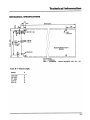
1
SBS–2400H
User’s Manual
Part #02416
Rev 0592
OCTAGON SYSTEMS®
6510 W. 91st Avenue Westminster CO 80030 USA
TEL: 303–430–1500 FAX: 303–426–8126 Tech Support: 303–426–4521
COPYRIGHT
NOTICE TO USER
Copyright 1989–93—Octagon Systems. All
rights reserved. However, any part of this
document may be reproduced provided that
Octagon Systems Corporation is cited as the
source.
The information contained in this document is
believed to be correct. However, Octagon
assumes no responsibility for any of the circuits
described herein, conveys no license under any
patent or other right and makes no representations that the circuits are free from patent
infringement. Octagon makes no representation or warranty that such applications will be
suitable for the use specified without further
testing or modification.
The contents of this document and the specifications herein may change without notice.
TRADEMARKS
Octagon Systems general policy does not
recommend the use of its products in life
support applications where the failure or
malfunction of a component may directly
threaten life or injury. It is a Condition of Sale
that the user of Octagon products in life support
applications assumes all the risk of such use
and indemnifies Octagon against all damages.
Octagon Systems™, the Octagon logo,
CAMBASIC™ and PC SmartLINK™ are
trademarks of Octagon Systems.
IBM PC™ is a registered trademark of IBM.
Microsoft BASIC™ is a trademark.
Opto 22™ is a trademark of Opto 22.
2
SBS-150-RI, SBS-250-R3, SBS-2300-R3,
SBS-2400-R1, SBS-R5, 7100-R5, 7200-R1, 8410-R2
8420-R1, 9500/9510-R3, 9600-R1-2/90
Autorun Notice
Effective 2–19–90
Octagon does not recommend autorunning from system RAM. System noise will eventually corrupt the
program and cause it to crash. If you wish to autorun from RAM, do so only as an interim method or over
a short period of time.
Table Of Contents
Preface
Chapter 4—Serial Ports
Manual Organization ..................................... i
SYMBOLS AND TERMINOLOGY .................... i
PRODUCT SUPPORT ....................................... ii
Technical Support ......................................... ii
DESCRIPTION .............................................. 4–1
Console Port—(J1) ..................................... 4–1
Primary Port—(J4) .................................... 4–2
RS-422 Port—(P3) ..................................... 4–3
SERIAL PORT FILE NUMBERS ................. 4–3
CHANGING THE BAUD RATE ................... 4–3
SERIAL I/O COMMANDS ............................ 4–3
Chapter 1—Overview
SBS–2400 DESCRIPTION ............................ 1–1
MAJOR FEATURES ..................................... 1–1
Chapter 2—Setup and Operation
OPERATING PRECAUTIONS ..................... 2–1
GETTING STARTED .................................... 2–1
DEVELOPMENT SYSTEM SETUP ............. 2–2
Installing Your Equipment ....................... 2–2
SYSTEM SETUP ........................................... 2–3
Installing Your Equipment ....................... 2–3
TROUBLESHOOTING ................................. 2–4
No Power to SBS–2400 ............................. 2–4
No Sign–On Message ................................ 2–4
Test Program Does Not Work ................... 2–4
Chapter 5—Memory Sockets
MEMORY DEVICES ..................................... 5–1
EPROM ...................................................... 5–1
EEPROM ................................................... 5–1
Battery–Backed RAM ............................... 5–1
DS–1213C & DS-1213D SMARTSOCKETS . 5–1
DS–1216EM REAL TIME CLOCK ............. 5–1
SAVING PROGRAMS IN NONVOL. MEMORY 5–2
Saving Programs To EPROM ................... 5–2
Saving Programs to EEPROM or BB RAM 5–3
COMBINING PROGRAM AND DATA ........ 5–3
WRITE–PROTECTION ................................. 5–4
LOADING PROGRAM INTO RAM .............. 5–4
Chapter 6—Speaker Output
Chapter 3—Parallel I/O Lines
J2 I/O LINES DESCRIPTION ...................... 3–1
J3 I/O LINES DESCRIPTION ...................... 3–1
J3 High Current Outputs ......................... 3–1
CONSIDERATIONS .................................... 3–1
INTERFACING TO AN OPTO MODULE
RACK .............................................................. 3–2
INTERFACING TO SWITCHES .................. 3–2
CONFIGURING PARALLEL I/O LINES .... 3–3
PROGRAMMING EXAMPLE—J2 ............... 3–3
Program Explanation ................................ 3–3
COMMANDS ................................................. 3–3
DESCRIPTION .............................................. 6–1
Connecting a Speaker to the SBS–2400 ... 6–1
PROGRAMMING EXAMPLE ....................... 6–1
Chapter 7—Keypad Port
DESCRIPTION .............................................. 7–1
Scanning the Keypad ................................ 7–1
PROGRAMMING EXAMPLE ....................... 7–1
Program Explanation ................................ 7–1
COMMANDS ................................................. 7–1
1
Table Of Contents
Chapter 8—Counter Inputs
SOFTWARE COUNTER/TIMERS ............... 8–1
Using CAMBASIC II for Counter Control .. 8–1
PROGRAMMING EXAMPLE ....................... 8–1
Program Explanation ................................ 8–1
HARDWARE COUNTER/TIMERS .............. 8–2
COMMANDS ................................................. 8–3
Chapter 9—Interrupt Inputs
DESCRIPTION .............................................. 9–1
Interrupt Generation ................................ 9–1
PROGRAMMING EXAMPLE ....................... 9–1
Program Explanation ................................ 9–2
COMMANDS ................................................. 9–2
Chapter 10—Analog Outputs
OPTO-ISOLATORS ......................................... A–3
ACCESSORIES ............................................ A–4
Appendix B—Technical Info.
TECHNICAL SPECIFICATIONS ...............
MECHANICAL SPECIFICATIONS ............
JUMPER DESCRIPTIONS ..........................
MEMORY MAP ............................................
I/O MAP ........................................................
CONNECTOR PINOUTS .............................
Console Serial Port (J1) ...........................
Parallel I/O Port (J2) ................................
High Current Output Port (J3)................
Primary Serial Port (J4) ..........................
Keypad Port (J5) .......................................
Analog Output Port (J6)...........................
Counter/Timer Input Port (J7) ................
Expansion Bus Edge ................................
B–1
B–3
B–4
B–5
B–5
B–5
B–5
B–5
B–6
B–6
B–6
B–6
B–6
B–7
DESCRIPTION ............................................ 10–1
Installing an Anolog Channel ................. 10–1
Sending Data to an Analog Output ........ 10–1
Power Supply Requirements .................. 10–1
COMMANDS ............................................... 10–1
Appendix C—82C54 Data Sheet
Chapter 11—Watchdog Timer
SBS–2400 ...................................... PAGE 1 OF 3
SBS–2400 ...................................... PAGE 2 OF 3
SBS–2400 ...................................... PAGE 3 OF 3
DESCRIPTION ............................................ 11–1
OPERATION ................................................ 11–1
Appendix A—Options and Accessories
USING THE SBS–2400 W/O CARD CAGE A–1
ADDING CUSTOM CIRCUITRY ................ A–1
ADDING I/O LINES ..................................... A–1
Sup–6C Counter and I/O Card ................ A–1
Sup–7C Expansion Card .......................... A–1
CREATING A CUSTOM COMM. CABLE .. A–1
USING OTHER COMM. SOFTWARE ........ A–2
USING SBS–2400 IN MULTIDROP NETWORK A–2
AUTORUNNING OPTIONS ........................ A–2
Disabling the Autorun Feature ............... A–2
Loading a Program w/o Autorunning ...... A–2
2
Schematics
Warranty
Preface
This manual provides all the information
required to install, configure and operate the
SBS–2400 Microcontroller.
Chapter 7
Presents technical information
on the Keypad Port.
Chapter 8
Presents technical information
on the Counter Inputs.
Chapter 9
Presents technical information
on the Interrupt Inputs.
Chapter 10
Presents technical information
on the Analog Outputs.
Chapter 11
Presents technical information
on the Watchdog Timer.
Appendix A
Presents technical information
on options and accessories for
the SBS–2400.
Appendix B
Presents technical specifications, jumper information,
memory and I/O maps, and
connector pinouts for the SBS–
2400.
With this information you can accomplish the
following:
1. Set up communications between the
SBS–2400 and a terminal or PC.
2. Interface the SBS–2400 to the Expansion Bus and peripheral cards.
3. Gain an understanding of the operation
of the SBS–2400 hardware using
CAMBASIC II programming software.
This manual assumes that you are familiar
with some type of BASIC programming software. If you have not used this language, refer
to the CAMBASIC II Programming Guide
for information and examples of all the commands.
NOTE: The SBS–2400 uses a 64180 processor.
Additional information on this component can be obtained from your local
Hitachi representative (hardware
manual #U77, software manual #U92,
phone: 800–447–8440).
Schematics
Warranty
SYMBOLS AND TERMINOLOGY
Manual Organization:
Chapter 1
Chapter 2
Chapter 3
Describes the SBS–2400 Microcontroller and its major features.
Presents setup and operation
information for the SBS–2400
Development System as well as
information for installing
systems with nonOctagon
components.
Presents technical information
on the Parallel I/O Lines.
Chapter 4
Presents technical information
on the Serial Ports.
Chapter 5
Presents technical information
on the Memory Sockets.
Chapter 6
Presents technical information
on the Speaker Output.
Throughout this manual, the following symbols
and terminology are used:
< >
W[
A character within “< >”
indicates a single key.
– ]
Denotes a jumper block
and the pins to connect.
NOTE:
Information under this
heading presents helpful
tips for using the SBS–
2400.
CAUTION
Information under this
heading shows you how
to avoid potential
problems.
i
Preface
WARNING
Information under this
heading warns you of
situations which might
cause catastrophic or
irreversible software or
hardware damage.
Autorun
Automatic execution of a
program on power up or
reset.
Download
Transferring a program
or data from a PC to the
SBS–2400.
Free Memory
The amount of memory
available for program
and data storage.
Industrial Command
Specialized CAMBASIC
II
commands designed for
industrial programming
applications e.g. AIN,
AOT, BIT.
Extensions
Multidrop Network
A method of multiprocessor communication using RS–485.
PC
Any personal computer
with terminal emulation
software, such as an
IBM PC™ with PC
SmartLINK™.
PC SmartLINK
Refers to all versions of
PC SmartLINK.
Reset
Resetting the SBS–2400
hardware or software by
pushing its reset switch.
Stand Alone Mode
SBS–2400 is not connected to peripheral
equipment via a bus.
System RAM
Memory used by CAMBASIC II for maintenance and operating
functions.
Terminal
Any “dumb” terminal,
such as a Wyse 30 or
VT–100.
2ii
TTL Compatible
0 to +5V logic levels.
Upload
Transferring a program
or data from the SBS–
2400 to a PC.
XON/XOFF
A sender/receiver
protocol in which data
transmission is suspended until the receiving device is ready to
accept the incoming
information.
&
A prefix “&” denotes a
hexadecimal number. A
decimal number has no
prefix. For example,
&1000 and 4096 are
equivalent.
PRODUCT SUPPORT
If you have a question about the SBS–2400
Microcontroller and can’t find the answer in
this manual, call Technical Support. They will
be ready to give you assistance.
When you call, please have the following at
hand:
●
Your SBS–2400 User’s manual
●
A description of your problem
Technical Support:
PHONE:
303–426–4521
FAX:
303–426–8126
HOURS:
Eastern
Central
Mountain
Pacific
11–2 & 3–6
10–1 & 2–5
9–12 & 1–4
8–11 & 12–3
Chapter 1
Overview
SBS–2400 DESCRIPTION
MAJOR FEATURES
The SBS–2400 Microcontroller is a 4.5" x 8"
computer board that contains all the hardware
and software necessary to create a control
system. It uses a 64180 CPU (9.216 MHz) and
can be operated in a stand–alone mode or in
conjunction with other peripheral boards.
The SBS–2400 comes with CAMBASIC II
software for program development. This
language was specifically developed for control
and data acquisition applications. For a
complete description of CAMBASIC II and its
commands, refer to the CAMBASIC II Programming Guide.
If you wish to use your PC’s editing and merging features for program development, the
SBS–2400 can be linked to your PC using PC
SmartLINK. For a complete description of PC
SmartLINK and its operation, refer to the PC
SmartLINK Manual.
●
Resident CAMBASIC II Software
The SBS–2400 provides CAMBASIC II
software for program development.
This software is designed for developing
control and data acquisition programs.
Its syntax is very similar to Microsoft
BASIC™. However, industrial command extensions have been added to
help you interface with both built–in
and external real time hardware.
●
Autoruns On Power Up
Autorun refers to the automatic execution of a program on power up or reset.
Autorun programs can be stored in
EPROM, EEPROM or battery–backed
RAM and will automatically execute
when placed in socket U3.
●
AutoBaud
The autobaud feature automatically
determines and operates at the baud
rate of your terminal or PC.
RS–232
Interface
Data Bus
Address
Bus
64180
CPU
2–channel
D/A
Converter
Option
16 Digital
I/O Lines
RS–422
Interface
3–channel
Counter/
Timer
32K/128K
System RAM
CAMBASIC II
ROM
J4
Primary
Serial Port
P3
RS–422
Serial Port
J6
Analog Output
Port
J5
Keypad Port
High Current
Drivers
Control Bus
J1
Console
Serial Port
32K RAM
EPROM/
EEPROM
Socket
24 Digital
I/O Lines
Push Button
Reset
J3
8–Channel
High Current Port
J2
24–Channel
Digital I/O Port
J7 CTC
I/O Port
Figure 1–1—SBS–2400 Block Diagram
1–1
Overview
●
Serial Ports
The SBS-2400 has two programmable
RS–232 serial ports. Baud rate, parity,
length, and number of stop bits are
software programmable for both ports
using the CONFIG COM$ command.
●
Keypad Port
The keypad port accepts a 4 x 4 matrix
keypad. The keypad is automatically
scanned and can be read using the
KEYPAD$ command. When a key is
pressed, a software interrupt is generated.
●
Real Time Clock Support
An optional battery–backed calendar
clock module can be installed on the
SBS–2400. The time resolution is 0.01
seconds. Both the time and date are
readable.
An additional timer output can be
provided via the 82C54. This output
can be connected to a 9.216 MHz input
and cascaded to give a range of over 400
seconds.
●
●
High Current Outputs
The SBS–2400 has eight high current
sinking outputs for driving relays,
lamps, small solenoids, etc.
●
On–Card Programmers
Once your program has been debugged,
it can be stored into an EPROM or
EEPROM device using the on–card
programmer.
●
Pulse Width Modulators
The SBS–2400 has four pulse width
modulation (pwm) outputs. Two of the
outputs are controlled through software
and two can be configured via the
82C54. The ON and OFF times are
independently variable.
●
●
1–2
Software Event Counters
There are eight event counters which
can accumulate up to 65,535 events.
These are a part of the CAMBASIC II
multitasking system. They operate over
a 0–40 Hz range and can generate a
software interrupt on a preset count.
Timer Outputs
Up to eight I/O lines can be designated
as software timed outputs with a range
of 0.01 to 655.35 seconds. These are a
part of the CAMBASIC II tasking
system.
Counter Inputs
The SBS–2400 provides nine software
and three hardware counters. Eight of
the software counters are a part of the
multitasking operating system and will
count events. They accept count rates
from 0 to 40 Hz. The remaining software counter is interrupt–driven and
can accept count rates from 0 to 2 kHz.
The three 16–bit, hardware counters
are supplied from a 82C54. These
counters are programmable and can be
configured as frequency inputs, PWM
outputs, and high speed counters.
Frequencies as high as 10 MHz can be
measured. Optionally, these outputs
can interface to opto–isolated input
signals.
●
Analog Outputs
There are two optional analog outputs
with 12 bits of resolution. Three output
ranges are available: 0–5V, 0–10V, and
+5V.
●
Parallel I/O Lines
The SBS–2400 has 40 parallel I/O lines
which are logic level compatible and can
drive Opto 22™ style modules.
●
Data Storage
The SBS–2400 provides space for as
much as 512K of RAM for storing and
retrieving your process data. The RAM
can be optionally battery–backed. The
maximum program size does not increase beyond 32K (EPROM limited).
●
Battery–Backed Memory
The Battery–backed RAM option
automatically saves your process
variables and data when power fails.
●
Watchdog Timer
A watchdog timer is provided as a
failsafe against program crashes or
processor lockups. The watchdog will
reset the SBS–2400 approximately
every 150 mS unless reset by an I/O
read at address (&E8).
Chapter 2
Setup and Operation
OPERATING PRECAUTIONS
GETTING STARTED
The SBS–2400 contains static sensitive CMOS
components. To avoid damaging these components, observe the following precautions before
installing your SBS–2400 system:
Before installing your SBS–2400, become
familiar with the location of various connectors
and jumpers. Refer to Figure 2–1.
Throughout this manual there are references to
jumper block W1 and W6. The jumpers configure the modes of the device located at U2 and
U3.
1) GROUND YOURSELF BEFORE
HANDLING THE SBS MICROCONTROLLER OR PLUGGING IN
CABLES.
Table 2–1 shows the jumpers associated with
each device.
2) DO NOT REMOVE OR INSERT THE
SBS–2400 FROM A CARD CAGE
WITH THE POWER APPLIED.
Table 2–1 — U2 Memory Device Size
Jumper
Socket U2
Description
____________________________________________
3) DO NOT INSERT OR REMOVE
COMPONENTS WHEN POWER IS
APPLIED.
W6–default
[1–2]
32K or 128K RAM
device
W6–option
[2–3]
256K or larger RAM
device
When burning an EPROM or EEPROM,
place the components in their sockets
before applying power. However, you
can install or remove jumpers when the
power is applied.
RS–232/422
Select
R–
U13
T–
GD
W5
U15
W4
W1
U10
U5
WD
1
U6
2
Watchdog Timing
(hardwired
jumpers)
J6
W2
P2
U7
Alternate
+5V Input
2
21
U4
1
U18
U19
W3
DAC Voltage Analog Output
Supply Select Range Select
Parallel
I/O Port
Pushbutton
Reset
J7
U17
1
1
U3 RAM/ROM
Select
J2
Counter/Timer
Configuration
Analog
Output Port
J5
Keypad
Port
J3
U24
U9
U16
U3
User RAM/ROM 1
U23
High Current Driver/
Keypad Interface
2
1
J1
Console Serial
Port
U22
Parallel I/O Lines
R+
U12
U20
64180 CPU
U2
System RAM
T+
U21
U8
W6
1
Primary Serial
Port
J4
XTAL
U1
CAMBASIC II
U2 System
RAM Size
RS–422
Port
High Current
Output Port
Counter/Timer
I/O Port
Figure 2–1—SBS–2400 Component Diagram
2–1
Setup and Operation
Table 2–2 — U3 Memory Device Type
Jumper
Socket U3
Description
____________________________________________
W1–ROM
configurations
W1–RAM
configurations
NOTE:
[1–2]
[6–7]
[9–10]
EPROM programming
voltage
Programming Control
Chip select
[2–3]
[5–6]
[9–10]
RAM address line
RAM WRITE line
Chip select
Pins 4 and 8 are nonfunctional and never used.
DEVELOPMENT SYSTEM SETUP
If you ordered a development system, it will
contain all the necessary components to get a
system up and running in just a few minutes.
Follow the installation instructions in this
section if you have a SBS–2400 development
system or the following Octagon components:
●
●
●
●
●
SBS–2400 Microcontroller
PS–1020 Power Supply
EB–3000 Enclosure Base
VTC–series serial cable for your PC
PC SmartLINK software.
If you have neither of these configurations,
refer to “SYSTEM SETUP” in this chapter.
Installing Your Equipment:
The SBS–2400 jumpers are set to match PC
SmartLINK communications software. Jumper
changes are not necessary to operate your
system.
1. Place the EB–3000 Enclosure Base
before you with the rubber feet resting
on the table surface.
2. Place the PS–1020 Power Supply in the
bottom slot, making sure that the unit
is pushed completely into the connector
on the EB–3000. Confirm that the
POWER and PROGRAM switches are
in their OFF positions.
3. Plug the power cord on the PS–1020
into a 120 VAC source.
2–2
4. Place the SBS–2400 into the top slot of
the card cage so that the components
are facing up.
5. Ground yourself and plug the 10–pin
connector on the serial cable into J1 on
the SBS–2400. This is the Console
serial port.
Plug the other connector into COM1 of
your PC. If your PC has only one serial
port, it is probably COM1. If you have
two serial ports, check your computer
manual to see which is COM1. If you
are already using COM1, you can use
COM2. Refer to the PC SmartLINK
Manual for information on using COM2
rather that COM1.
6. Place your PC SmartLINK disk into
drive “A:” and type.
A:SL
Press <ENTER> and PC SmartLINK
will initialize your PC to match the
SBS–2400.
7. Move the power switch on the PS–1020
to the ON position. A green LED will
light.
8. In a few seconds a logon message will
display similar to the following (assuming the baud rate is set to 9600):
CAMBASIC II (tm) (c) 1985–90
Octagon Systems Corporation
All
rights
reserved
Vers 3.xx–24 - Free _
9. Press the <ESC> key. A logon message
will display showing the current version
of CAMBASIC II and the amount of free
memory available. If you have more
than 32K of RAM in the system, more
memory will be shown and an additional message will confirm its existence.
CAMBASIC II (tm) (c) 1985-90
Octagon Systems Corporation
All
rights
reserved
Vers 3.xx–24 - Free - 29950
Setup and Operation
10. The system is now ready for you to start
programming. If the system has not
responded as described, refer to
“TROUBLESHOOTING” in this chapter.
11. Type in the following test program:
10
20
30
40
FOR X=0 TO 2
PRINT “Hello
NEXT
PRINT
“;
12. Type RUN. The system will display:
range. Any well–regulated supply that
can furnish at least 100 mA at +5V and
±40 mA at ±12V can be used. “Switching” power supplies are not recommended since analog output voltage
may exhibit switching noise. With the
supply off, connect the +5V lead to pins
1 and A of a 44–pin connector (CE–44).
Connect the ground lead to pins 22 and
Z. Connect the +12V lead to pin X and
the –12V lead to pin 21. Place a normally open switch between pins X and
20. This is used to switch the programming voltage. Place the connector on
P1.
Hello Hello Hello
_
This concludes the quick setup using a development system. If you have a hard disk, you may
want to move PC SmartLINK to drive “C:”.
Refer to the PC SmartLINK Manual for more
information.
Chapter 3 contains the information necessary to
connect your card to external I/O devices.
3. The serial cable for the SBS–2400 is
terminated with a 10–pin IDC connector on the SBS–2400 end and a connector that is appropriate to the PC or
terminal that you are using. Plug the
10–pin connector on the cable into J1 on
the SBS–2400.
Refer to Appendix A, “Creating a
Custom Communications Cable”, if you
will be making your own cable.
4. You can use either a PC or CRT terminal as a programming device.
SYSTEM SETUP
If you are using components other than those
listed below, use the following instructions to
install your SBS–2400:
●
●
●
●
PS–1020 Power Supply
EB–3000 Enclosure Base
VTC–series serial cable for your PC
PC SmartLINK software
Installing Your Equipment:
SBS–2400 jumpers have been set at the factory
for the most common configuration. Jumper
changes are not necessary to operate your
system.
1. Make sure that the SBS–2400 is not
laying on a conducting surface. It is
advisable to mount standoffs in each
corner of the board.
2. The SBS–2400 needs a +5V and +12V
supply. –12V is also required if you are
using analog outputs with the ±5V
Using a PC:
Plug the other end of the serial cable
into COM1 of your PC. If your PC has
only one serial port, it is probably
COM1. If you have two serial ports,
check your computer manual to see
which is COM1. If you are already
using COM1, you can use COM2. See
the PC SmartLINK Manual for
information on using COM2 rather that
COM1. If you are not using PC
SmartLINK, refer to Appendix A,
“Using Other Serial Communications
Software”.
Using a Terminal:
Follow the terminal instruction manual
and initialize your terminal to 9600
baud, 8 data bits, no parity and 1 stop
bit. If your terminal cannot operate at
this baud rate, the SBS–2400 will adapt
to 1200, 2400, 4800, or 19.2K baud. The
number of data bits, parity and stop bits
remain the same.
2–3
Setup and Operation
5. After connecting the terminal or PC to
the SBS–2400, you are ready to establish communications. Turn on your
terminal or boot up your communications program on your PC.
6. Turn on your power supply. On power
up a copyright message is printed. If a
nonsense message appears, your terminal is not set at 9600 baud. In either
case, press the <ESC> key. The system
will adapt to your baud rate and display
a logon message showing the current
version of CAMBASIC II and the
amount of free memory available:
CAMBASIC II (tm) (c) 1985-90
Octagon Systems Corporation
All
rights
reserved
Vers 3.xx–24 - Free -29950
If you don’t get the proper logon, check
the serial parameters (other than the
baud rate) to make sure they are set
correctly. If the system still does not
respond, refer to “TROUBLESHOOTING” in this chapter.
7. The system is now ready for you to start
programming.
8. Type the following test program:
10
20
30
40
FOR X=0 TO 2
PRINT “Hello “;
NEXT
PRINT
TROUBLESHOOTING
No Power To SBS–2400:
1. Make sure the power cord is properly
connected between the power supply
and SBS–2400.
2. If you are using a PS–1020 Power
Supply, make sure its fuse (located
under the power transformer) is not
blown.
No Sign–On Message:
1. Check the serial parameters on your PC
or terminal. The default setting should
be:
9600 baud, no parity, 8 data bits, 1
stop bit
2. Make sure the serial cable is properly
connected between the SBS–2400 and
your PC or terminal.
3. Make sure the serial cable is working
properly by performing a point–to–point
check on the connectors. Refer to Table
A–1 in Appendix A for corresponding
connector, signal and pin numbers.
4. Make sure the SBS–2400 is receiving
power. It requires +5V and +12 VDC. –
12V is also required if you are using
analog outputs with the ±5V range.
Test Program Does Not Work:
9. Type RUN. The system will display:
Hello Hello Hello
_
NOTE: If you are using a terminal and program
development takes more than one day,
you should consider saving your program to on–card memory. This allows
you to retrieve your program at a later
date. Refer to Chapter 5, Memory
Sockets, for information on saving
programs to memory devices.
2–4
If you are using PC SmartLINK and the test
program does not work, call the Octagon Technical Support Department.
If you are using other serial communications
software and your test program does not work,
it is probably due to noncommunication between the PC and the SBS–2400. To verify that
the SBS–2400 is communicating with your PC:
1. Connect an oscilloscope to U12, pin 8 on
the SBS–2400.
2. Press any key on the PC keyboard to
verify that the signal switches between
+5V and ground.
Setup and Operation
3. If the signal does not switch between
+5V and ground, check U12, pin 10 on
the SBS–2400 for a signal change of at
least ±3V.
4. If you cannot get a signal at U12, pin
10, check your computer and make sure
it is transmitting.
If you are using a communications package
other than PC SmartLINK, note the following:
●
The SBS–2400 does not send a CTS
signal to the host. Your PC or terminal
must tie this line high. If your terminal
or communications software requires
other signals (DCD, DSR), you may
have to tie these signals to the appropriate levels. You may be able to ignore
these lines in software.
2–5
Setup and Operation
2–6
Chapter 3
Parallel I/O Lines
WARNING
APPLY POWER TO THE SBS–2400
BEFORE APPLYING AN INPUT VOLTAGE TO THE PARALLEL I/O LINES.
This prevents excessive currents from
flowing and damaging input devices. If you
cannot apply power to the SBS–2400 first,
contact the Technical Support Department
for suggestions appropriate to your application.
J2 I/O LINES DESCRIPTION
An 82C55 (U22) is used to control 24 parallel I/
O lines at connector J2. All lines are TTL logic
level compatible (0 to +5V) and have 10K pull–
up resistors. I/O address is 40H-43H.
The three ports of the 82C55 are organized as
follows:
Port A
Eight lines that can be programmed
as all inputs or all outputs. Directly
interfaces to connector J2. I/O
address is 0.
Port B
Eight lines that can be programmed
as all inputs or all outputs. Directly
interfaces to connector J2. I/O
address is 1.
Port C
Eight lines which can be programmed in one group of eight lines
or two groups of four lines as all
inputs or all outputs. Bits 0 and 1 of
Port C can be used as inputs,
outputs, interrupts, or a counter. I/
O address is 2. Refer to Chapter 8,
“Counter Inputs,” for more information.
J3 I/O LINES DESCRIPTION
An 82C55 (U23) is used to control 8 parallel
output lines at connector J3. All lines are TTL
logic level compatible (0 to +5V) and have 10K
pull–up resistors. These lines interface to a
high current driver and connector J3. I/O
address is 0-3.
All eight lines can be used as general purpose
TTL I/O lines by replacing the 2804 at U24 with
a dip shunt jumper.
J3 High Current Outputs:
The eight I/O lines at J3 (pins
1,3,5,7,9,11,13,14) can be used as high current
drivers. These outputs will switch loads to
ground.
NOTE: When on, the saturation voltages are
incompatible with TTL logic levels and
should not be used to drive other logic
devices.
The logic outputs from the high current port are
inverted. That is, a “1” or “ON” written to the
high current port causes the output to switch on
or go low. The output driver chip, U24, can be
replaced with DIP shunt jumpers so that it is
TTL compatible like the other ports.
CONSIDERATIONS FOR HIGH CURRENT OUTPUTS:
●
Each of the high current outputs can sink
500 mA at +50V. However, the package
dissipation will be exceeded if all outputs
are used at the maximum rating. The
following conservative guidelines assume
the number of outputs are on simultaneously:
3–1
Parallel I/O Lines
# of Outputs
Max Current per Output
_______________________________________________________
1
500 mA
2
400 mA
3
275 mA
4
200 mA
5
160 mA
6
135 mA
7
120 mA
8
100 mA
Since the thermal time constant of the
package is very short, the number of outputs that are on at any one time should
include those that overlap even for a few
milliseconds.
●
●
Incandescent lamps have a “cold” current of
11 times that of its “hot” current. It is
recommended that lamps requiring more
than 50 mA not be used.
●
When inductive loads are used, protection
diodes or other schemes must be used.
Refer to Figure 3–1.
+ Supply
WARNING
If external devices, such as 24 VDC relays
are driven, the ground of the external +24V
supply must be connected to J3, pins 4, 6, 8,
10, or 12 and NOT the digital ground.
Failure to do so will produce a ground loop
within the SBS–2400 and can cause erratic
operation.
INTERFACING TO AN OPTO–MODULE
RACK
Parallel I/O lines can be interfaced to an 8–, 16–
or 24–position opto–module rack with an ORI–
24 cable assembly. One end of the ORI–24
plugs into J2 and the other plugs into a PB–8,
PB–16, or PB–24 mounting rack. Ground and
+5V are furnished through the ORI–24. However, it is recommended that a separate line be
run to +5V and ground on the opto–module
rack.
Use the following table to determine the corresponding opto channel for a particular 82C55
port:
OPTO
Channels
J2, 82C55
Port
I/O
Address
______________________________________
1N4002
(To High Current Output)
Figure 3–1 — Inductive Load Protection
Circuitry
●
3–2
Paralleling outputs for higher drive is NOT
recommended and could result in damage
since the outputs will not share current
equally.
0–3
4–7
8–15
16–23
Lower C
Upper C
A
B
2
2
0
1
INTERFACING TO SWITCHES OR
OTHER DEVICES
The UTB–26 and UTB–14 terminal boards
provide a convenient way of interfacing
switches or other parallel I/O devices to a
82C55 converter on the SBS–2400. I/O lines at
connector J2 can be connected to the UTB–26
with a CMA–26 cable. I/O lines at connector J3
can be connected to the UTB–14 with a CMA–
14 cable. Parallel I/O devices are then connected to the screw terminals on the UTB
board.
Parallel I/O Lines
CONFIGURING PARALLEL I/O LINES
COMMANDS
On power up or reset, all parallel I/O lines are
inputs. All lines have 10K pull up resistors to
the +5V supply. To reconfigure I/O lines as
outputs, use the CONFIG 4 and CONFIG 5
command. When a line is configured as an
output, it can sink a maximum of 2.5 mA at
+0.4V and can source a minimum of 2.5 mA at
+2.4V. When driving opto modules, the output
can sink 15 mA at 1.0V. Refer to the
CAMBASIC II Programming Guide for
configuring information.
Table 3–1 shows the CAMBASIC II commands
used for parallel I/O functions:
PROGRAMMING EXAMPLE—J2
PARALLEL I/O
10 ..Connect a UTB–26 to J2
20 CONFIG 4,0
30 CONFIG 5,0,0,0,1,1
40 ..Perform other initialization
routines
100 OUT 0,1
110 D = INP(2)
120 B = BIT(2,1)
130 BIT 1,3,1
Program Explanation:
20
30
100
110
120
130
Tells CONFIG 5 where 8255 is located
Configures 8255 ports A & B as low
outputs, C as all inputs
Sets Port A, bit 0 to a 1
Reads all lines on Port C
Reads Port C, bit 1
Turns on bit 3 of high current port
Table 3–1 — Parallel I/O commands
Command
Function
________________________________________________________________________
BIT
Function returns status of bit at I/O
address
BIT
Statement sets a bit to 0 or 1 at an I/O
address
CHAN
Reads status of opto–isolated module
CONFIG 4
Sets address for 8255 driver and CHAN
and OPTO commands
CONFIG 5
Initializes 8255 drivers at J2
CONFIG 8
Initializes 8254 at J7.
CONFIG COUNT Configures an I/O line for a counter input
CONFIG FREQ
Sets I/O address of the frequency inputs
CONFIG TIMER Configures an I/O line for a timed output
DINP
Returns 16–bit value from I/O
DOUT
Writes 16–bit value to I/O
FREQ
Measures frequency at an I/O port
INP
Returns a byte from I/O
ON BIT
Declares I/O line to monitor logic level
OPTO
Controls opto–isolated output modules
OUT
Writes a byte to I/O
PWM
Outputs a pulse width modulation signal
to an I/O port
NOTE: For Port A on J3, a “1” turns on a high
current line while a “0” turns it off.
3–3
Parallel I/O Lines
3–4
Chapter 4
Serial Ports
DESCRIPTION
The SBS–2400 has two serial ports that can be
used for interfacing to a printer, terminal or
other serial device. The Console port is used
primarily for program development. During
run time it can be used for other functions. The
Primary port can be used for interfacing the
SBS–2400 to a multidrop network or to devices
that require handshaking. Both ports support
XON/XOFF protocol to slow down data transmissions. The RS–422 port (P3) is used for
interfacing the SBS–2400 to serial devices that
require long distance data transmission and use
the RS–422 communication standard.
Default parameters are 9600 baud, 8 data bits,
no parity, and 1 stop bit. These parameters can
be changed with the CONFIG 3 command.
Refer to the CAMBASIC II Programming
Guide for further information.
Console Port – (J1):
The console port is located at J1. A VTC–10
style cable is required. This port has an RTS
input line so that the receiving device can
control the output of the Console port.
CAMBASIC II provides a 256 character output
buffer that is interrupt driven and sends
characters out the serial port without slowing
down program execution. When you execute any
of the PRINT statements, the characters to be
printed are turned over to the multitasker for
transmission and CAMBASIC II continues
program execution. However, if you try to fill
the output buffer with more than 256 characters, program execution will stop until all the
characters have been sent to the buffer. Any
character from 0 to 255 can be transmitted.
An input character automatically generates an
interrupt and the character is then stored into a
256 byte input buffer. Thus, your program can
be executing simultaneously with the reception
of characters.
This port is normally used in programming the
SBS–2400. However, during run time it may be
used as a general purpose serial port. When
used for programming or with the INPUT
statement, it will only accept ASCII characters
with values from 0 to 127. When used with the
INKEY$ and COM$ functions, it will return all
data from 0 to 255.
You can access the buffer in three ways. You
may need to consult the CAMBASIC II Programming Guide for more information.
1) In the first method, executing the
INPUT statement will remove all
characters in the buffer up to the
terminator character and put them into
a CAMBASIC II variable.
In this mode you have access to the full
256 bytes. If the buffer is not read and
the buffer fills, all subsequent characters will be discarded. A possible
disadvantage of using the INPUT
statement is that the program will halt
until the terminator is received. If the
operator is on a coffee break . . . .
2) The second method is to use the
INKEY$ function. Characters may be
removed one at a time with this function. When the buffer is empty, a null
string will be returned.
In this mode you have access to the full
256 bytes. If the buffer is not read and
the buffer fills, all subsequent characters will be discarded. The INKEY$
function may be used anywhere in the
program.
3) The last method uses the multitasking
statement, ON COM$. When this is
executed, characters are automatically
buffered until a termination condition
(which you specify) is reached. The
program will then jump to a subroutine
that removes the entire string from the
buffer.
In this mode you have access to only
128 of the 256 bytes at a time. If the
number of characters in the buffer
reaches 128 before meeting your termination conditions, the program will still
jump to the subroutine mentioned
above. If the buffer is not read and the
buffer fills to 256 characters, all subsequent characters will be discarded. The
advantage of this method is that the
whole string is captured without halting
program execution.
4–1
Serial Ports
Primary Port–(J4):
The Primary port is located at J4. A VTC–10
style cable is required. This port can be used
for general purpose serial data transfer or when
the SBS–2400 is part of a multidrop communications network. Programming may not be
done through this port.
NOTE: W5 [5–6] must be jumpered to use the
Primary port. The RS–422 (P3) port
cannot be used when the SBS–2400 is
jumpered to use the Primary port
CAMBASIC II provides a 256 character output
buffer that is interrupt driven and sends
characters out the serial port without slowing
down program execution. When you execute
any of the PRINT statements, the characters to
be printed are turned over to the multitasker
for transmission and CAMBASIC II continues
program execution. However, if you try to fill
the output buffer with more than 256 characters, program execution will stop until all the
characters have been sent to the buffer. Any
character from 0 to 255 can be transmitted.
An input character automatically generates an
interrupt hand the character is then stored in a
256 byte input buffer. Thus, your program can
be executing simultaneously with the reception
of characters.
You can access the buffer in three ways. You
may need to consult the CAMBASIC II Programming Guide for more information.
1) In the first method, executing the
INPUT statement will remove all
characters in the buffer up to the
terminator character and put them into
a CAMBASIC II variable. Only characters from 0 to 127 can be used with he
INPUT statement.
In this mode you have access to the full
256 bytes. If the buffer is not read and
the buffer fills, all subsequent characters will be discarded. A possible
disadvantage of using the INPUT
statement is that the program will halt
until the terminator is received. If the
operator is on a coffee break . . . .
4–2
2) The second method is to use the
INKEY$ function. Characters may be
removed one at a time with this function. When the buffer is empty, a null
string will be returned. Any character
from 0 to 255
can be returned.
In this mode you have access to the full
256 bytes. If the buffer is not read and
the buffer fills, all subsequent incoming
characters will be discarded. The
INKEY$ function may be used anywhere in the program.
3) The last method uses the multitasking
statement ON COM$. When this is
executed, characters are automatically
buffered until a termination condition
(which you specify) is reached. The
program will then jump to a subroutine
that removes the entire string from the
buffer. Any character from 0 to 255 can
be returned.
In this mode you have access to only
128 of the 256 bytes at a time. If the
number of characters in the buffer
reaches 128 before meeting your termination conditions, the program will still
jump to the subroutine mentioned
above. If the buffer is not read and the
buffer fills to 256 characters, all subsequent characters will be discarded. The
advantage of this method is that the
whole string is captured without halting
program execution.
The RTS line may be read using the following
BASIC statement:
100 B = BIT (130,5)
The CTS line may be controlled to hold off the
sending device from transmitting. Use the
following BASIC statements:
400 BIT 128,4,1
500 BIT 128,4,0
Line 400 sets the CTS line low, requesting the
transmitting device to hold off. Line 500 sets
the CTS line high, signaling the transmitting
device it is OK to send.
Serial Ports
RS–422 Port–(P3):
CHANGING THE BAUD RATE
The RS–422 port is located at P3. This port is
designed to interface to serial devices that use
the RS–422 communications standard and
require long distance data transmission. RS–
422 serial connections to the SBS–2400 are
made through screw terminals on P3.
Use CONFIG 3 to change the baud rate of
the Console and Primary serial ports. 150K
and 38.4K baud rates are not available on
the SBS–2400.
NOTE: W5 [3–4] must be jumpered to use the
RS–422 port. The Primary port cannot
be used when the SBS–2400 is
jumpered to use the RS–422 port.
SERIAL I/O COMMANDS
Table 4–1 shows the CAMBASIC II commands
used for serial I/O functions:
Table 4–1—Serial I/O Commands
SERIAL PORT FILE NUMBERS
CAMBASIC II references the serial I/O ports by
file numbers. The following table shows the
corresponding file number to serial I/O port:
Description
File#
Example
Console Port (J1)
0
PRINT "hello" or
PRINT #0,
"hello"
Primary Port (J4)
"hello"
1
PRINT #1,
RS–422 Port (P3)
1
PRINT #1, "hello"
Command
Function
CLS
COM$
DISPLAY
INKEY$
INPUT
LIST
ON COM$
string
PRINT
PRINT!
PRINT$
TAB
Clears screen
Returns string from autobuffer
Sends data to serial display
Returns character from serial buffer
Receives data from serial port
Outputs program listing
Jumps to subroutine on serial
Outputs data through serial ports
Prints formatted strings or number
Prints list of numbers as characters
Tabs to specified position
4–3
Serial Ports
4–4
Chapter 5
Memory Sockets
MEMORY DEVICES
Programs and data can be saved to a 16K
EPROM or 8K or 32K EEPROM located in
socket U3. U2 is the system RAM and will
accept static RAM devices from 32K (supplied)
to 512K. 128K is currently available. 256K and
512K will be offered when available.
The following is a description of the types of
memory devices that are compatible with the
SBS–2400:
DS–1216EM REAL TIME CLOCK
The DS–1216EM Real Time Clock module is an
option with the SBS–2400. The Clock has a
built–in, dual battery system with a minimum
life of 5 years. Accuracy is 1 min./mon. at 25°
C.
WARNING
The DS–1216EM is a modified version of the
standard DS–1216E. The standard part will
not function properly and will be damaged
during EPROM programming.
EPROM:
Any 27C128 EPROM with a speed of 250 nS or
faster and a programming voltage of +12.5V.
EEPROM:
Any 28C64 (8K) or 28C256 (32K) EEPROM with
a speed of 250 nS or faster.
Battery–Backed RAM:
DS–1213C AND DS–1213D SMARTSOCKETS
The DS–1213C and DS–1213D SmartSockets
are options with this system. These modules
have DIP sockets with built–in power fail
circuitry and a dual battery system with a
minimum life of 5 years. The DS–1213C provides battery–backup for a low power, 32K
CMOS RAM. The DS–1213D provides battery–
backup for a low power, 128K CMOS RAM.
CAUTION
Do not put a DS–1216EM Real Time Clock
into the top of the SmartSocket. This will
seriously shorten the battery life of the
SmartSocket.
To install a SmartSocket on the SBS–2400:
1. Remove the existing RAM from the
socket you wish to use (U2 or U3.)
2. Install the SmartSocket into the empty
socket with the index mark pointing
towards the SBS–2400 contact fingers.
3. Install the RAM into the top of the
SmartSocket. Make sure pin 1 on the
RAM module is aligned with pin 1 of the
SmartSocket.
Real Time Clock Installation—
The U3 socket may contain either a 32K
EEPROM or 16K EPROM.
1. Jumper this socket for the device that
you will be using. Refer to Appendix B,
“Jumper Descriptions” for jumpering
information.
If you will not be using this socket for
memory, jumper:
W1 [1–2], [6–7], [9–10]
No other jumpers at W1 are used.
2. After the appropriate jumpering, install
the DS–1216EM in U3 with the index
mark on the Clock pointing towards the
SBS–2400 contact fingers.
3. Plug an EPROM or EEPROM into the
top of the Clock with the index notch on
the RAM pointing the same way.
4. The Clock is shipped with its internal
oscillator turned off to maximize battery
life. To turn it on, type:
TIME ON
You need to do this only once.
5. To test the Clock, type:
DATE 11,15,88,1
Then type:
PRINT DATE$(0)
5–1
Memory Sockets
6. If it prints out as shown below, the
Clock is working properly.
11/15/88
You can now set the time. For more
information see the CAMBASIC II
Programming Guide for the TIME,
DATE, TIME$ and DATE$ commands.
To make the memory nonvolatile,
remove the W1 [5–6] write–enable
jumper so that data cannot be accidentally written to this socket.
Refer to Appendix B “Jumper Descriptions” for
information on jumpering the SBS–2400 for the
above options.
Saving Programs To EPROM:
Writing to the Clock will not affect any EPROM
or EEPROM that may be plugged into it. The
write–enable jumper, W1 [5–6], does not need
to be installed to use the Clock. However, the
chip select jumper, W1 [9–10], must be installed. The DS–1216EM does not provide
battery–backup for a plug–in RAM, only for the
internal clock circuitry.
CAMBASIC II programs can be saved to a 16K
byte EPROM using the SBS–2400 on–board
EPROM programmer.
To save programs to EPROM:
1. Remove power from the SBS–2400.
2. Make sure the following jumpers are
installed:
SAVING PROGRAMS IN
NONVOLATILE MEMORY
Programs can be saved to a nonvolatile memory
device in socket U3. U3 is mapped as the lower
32K I/O addresses. CAMBASIC II moves a
program from U3 down into system RAM before
running the program. When your program is
finalized, the SAVE command can be used to
store the program to a memory device in U3.
The following are considerations for storing
your program to nonvolatile memory:
●
An autorun program may only reside in
socket U3.
●
Programs up to 8K can be stored in an
8K EEPROM (28C64).
●
Programs up to 16K can be stored in a
16K EPROM (27C128).
One advantage of using EEPROMs is
you do not need to erase them as you
would EPROMs. Another advantage is
that EEPROMs program much faster
than EPROMs. The disadvantage of
using EEPROMs is that they cost more
than EPROMs.
●
5–2
Programs up to 32K can be stored in a
32K RAM (43256C with DS–1213C) or a
32K EEPROM (28C256) in U3.
W1 [1–2], [6–7], [9–10]
No other jumpers at W1 are used.
3. Make sure the program switch on the
PS–1020 is OFF. The red LED should
NOT be on.
4. Install a 27C128 EPROM into socket U3
.
5. Apply power to the SBS–2400.
6. Download your program from the PC to
the SBS–2400 by following the download procedure in the PC SmartLINK
Manual.
7. Save your program in EPROM by
entering:
SAVE 0
8. The following prompt will be displayed:
+12V ON <ENT>
9. Turn on the PS–1020 PROGRAM
switch. The red LED on the PS–1020
will illuminate when the programming
supply is active, and the system will
begin programming the EPROM. Press
the <ENTER> key.
Memory Sockets
10. The next prompt will indicate the
number of bytes that will be saved. The
remaining bytes will be decremented
during programming.
xxxx bytes
If the EPROM fails to program, an error
message will display:
6. Save your program by typing:
SAVE 2
7. Since EEPROMs program quickly, no
time message is displayed. If the
program was stored, the following
message will display:
xxxx bytes
<Fail @ xxx>
NOTE: Programming takes approximately 20–40 mS per byte. The
total time to burn your program
depends upon program length
and EPROM characteristics. A
typical 16K program would take
about 8 minutes.
If the RAM or EEPROM fails to program, an error message will display:
–<Fail @ xxx>
8. To load the program back into RAM for
modification, type:
LOAD
11. When programming is complete, the
following prompt will display:
+12V OFF <ENT>
12. Turn off the PROGRAM switch on the
PS–1020 and press the <ENTER> key.
NOTE: Programming will be virtually
instantaneous for battery–
backed RAM and may take
several seconds for EEPROMs.
The exact speed depends upon
program length and EEPROM
characteristics.
13. To load the program back into RAM for
modification, type:
LOAD
Saving Programs To EEPROM Or
Battery–Backed RAM:
To save CAMBASIC II programs to EEPROM
or battery–backed RAM:
1. Remove power from the SBS–2400.
2. Install the jumpers as follows:
W1[2–3], [5–6], [9–10]
No other jumpers at W1 are used.
3. Install a memory device into socket U3.
4. Apply power to the SBS–2400.
5. Transfer your program to the SBS–2400
by following the download procedure in
the PC SmartLINK Manual.
COMBINING PROGRAM AND DATA
ON ONE MEMORY DEVICE
To save both program and data to a memory
device in U3, data must be placed in a memory
location that does not conflict with the memory
location of your program.
To determine an appropriate memory location
for your data:
1. Save your CAMBASIC program first
and record the number of bytes that are
displayed.
2. Use the following formula to determine
the address to start your data:
start address = &304 + program length
To save a block of data, you must use the
CAMBASIC II SAVE! command. Use the
starting address calculated above. Refer to the
CAMBASIC II Programming Guide for more
information.
5–3
Memory Sockets
The following program assumes that a program
or data has been put into RAM starting at
address &8500.
Data stored from &8500 to &8700 will be stored
to EPROM beginning at its address of &1000.
SAVE!
&8500,&8700,&1000
WRITE–PROTECTION
An EEPROM device or battery–backed RAM
can be write–protected by removing the following jumpers:
U1:
W1[5–6]
No other jumper changes are necessary.
Your program must be located below &1000 or
else the data saved to EPROM will be invalid.
One way to check for the end of a program in
EPROM is to execute the statement:
LOADING PROGRAMS INTO RAM
You may wish to load your autorun program
back into RAM for modification or reference.
PR%%&100
To load a program:
Pressing the space bar will cause the listing to
continue. Keep pressing the space bar until the
screen displays FF’s. This is the place to store
save to.
A 27C128 can save up to 16K bytes of data ,
resulting in a maximum address to the EPROM
of &3FFF. If your SAVE! is longer than the
EPROMs capacity, the lower addresses in the
EPROM will be over written and corrupted.
5–4
1. Enter:
LOAD
2. Your program will be transferred to
system RAM.
3. You can now view or modify your
program. If you change your program
and want to save the new version, refer
to “SAVING PROGRAMS TO EEPROM
OR BATTERY–BACKED RAM” in this
chapter. Make sure the write–enable
jumper is installed before saving your
program.
Chapter 6
Speaker Output
DESCRIPTION
PROGRAMMING EXAMPLE
Pin 16 on the Expansion Bus is the speaker
output from the 64180 CPU chip. This port can
be used to connect a speaker to the SBS–2400.
The SOUND command is used for frequency
generation. Refer to the CAMBASIC II Programming Guide for programming information.
The following generates a frequency at 1024 Hz
for a 10 second duration:
10 SOUND
1024,10
NOTE: The SOUND statement is cancelled
when program execution halts.
Connecting a Speaker to the SBS–2400:
Refer to Figure 6–1 for circuit connections to a
speaker. The series resistor determines the
volume. The capacitor size sets the lower
frequency limit. Generally, values from 100 µF
to 470 µF are adequate. The speaker can be
any impedance but those with 50 ohms or
greater will produce a higher sound level.
The output capability is limited to applications
with low ambient noise. An amplifier may be
required in some applications.
CAUTION
DO NOT connect pin 16 directly to a speaker,
ground or +5V, even momentarily, as damage
to the CPU may result.
Expansion Bus
pin 16
100 µF
100 ohm
+
To Speaker
Expansion Bus
pins Z, 22
Figure 6–1—Speaker Interface Circuitry
6–1
Speaker Output
6–2
Chapter 7
Keypad Port
DESCRIPTION
Connector J5 serves as the keypad interface to
the SBS–2400. The KP–1, KP–2, or KP–3
keypad can connect to J5 via a 10–pin cable
assembly supplied with the keypad.
Scanning the Keypad:
On power up, the keypad is configured with
lower port C as inputs and upper port C as
outputs. Scanning is enabled using the ON
KEYPAD$ command. The keypad is then
scanned every 80 mS which is the debounce
time. It can be changed using the CONFIG
KEYPAD$ command. The keypad value is read
into the interrupt subroutine declared by ON
KEYPAD$ using the KEYPAD$ function. You
can customize the response to the KEYPAD$
function by poking into memory locations
starting with the address returned by SYS(12).
Refer to the CAMBASIC II Programming
Guide for additional initializing and programming information.
Program Explanation:
10
40
50
500
510
540
570
Changes debounce time to 40 mS
rather than defaulting to 80 mS
Get address of keypad character
string, add offset to eighth key
Set up interrupt
Get keypad value
Clear buffer if “C” is pressed
Build string
The variable FL is a flag read by the
main program to determine if a
keypad string has been entered. The
flag should be cleared for subsequent
tests. B$ must be cleared before
subsequent characters are entered.
COMMANDS
Table 7–1 shows the CAMBASIC II commands
for the keypad:
Table 7–1 — Keypad Commands
Command
Function
______________________________________________________________
PROGRAMMING EXAMPLE:
The following example shows how to use each of
the functions and commands described above.
Your application may not need all of the commands.
10 CONFIG KEYPAD$ 4
20 ..optionally change a keypad
value.
30 .. change the “B” key to the
letter “M”
(ASCII
77)
40 POKE SYS(12) + 8,77
50 ON KEYPAD$ GOSUB 500
60 ..
70 GOTO 60
.
.
.
500 A$=KEYPAD$(0)
510 IF A$=”C” THEN B$=” “
520 IF A$=”#” THEN ..enter
530 PRINT A$;
540 B$=B$+A$
550 RETURN
560 ..enter
570 FL=1
600 RETURN
CONFIG KEYPAD$
KEYPAD$(0)
ON KEYPAD$
SYS(12)
Changes the debounce constant
Returns the last key from the
keypad port
Causes a program branch when a
key is pressed on keypad
Returns keypad string table
address
7–1
Keypad Port
7–2
Chapter 8
Counter Inputs
SOFTWARE COUNTER/TIMERS
The SBS–2400 has nine software counter/
timers that are designed to count low speed
events. Eight are part of the CAMBASIC II
multitasking system and accept count rates
from 0 to 40 Hz. One is interrupt driven and
designed to accept count rates from 0 to 2 kHz.
J2, pin 13 (or P1, pin 19 on the Expansion Bus)
is the software counter/timer input for the SBS–
2400. You can apply any TTL level signal up to
2000 Hz to this input. Changes faster than this
will be ignored. Counting occurs on a high to
low transition.
Before using a software counter, configure the
four bits of lower Port C (located on 82C55,
U22) as inputs. Use the CONFIG 4 and
CONFIG 5 commands to configure these ports.
Refer to the CAMBASIC II Programming
Guide for more information.
Using CAMBASIC II Commands for
Software Counter Control:
The CONFIG COUNT command is used to
define a software counter and has the following
syntax:
CONFIG COUNT number, address, bit
[,preset][,AUTO]
number is the counter number which ranges
from 0 to 8. Counters 0–7 are low speed
counter/timers and counter 8 is a high speed
counter/timer.
address is the I/O address of the port to serve as
the count input. The range is 0 to 255.
bit is the bit at that port which will act as an
input. This parameter ranges from 0 to 8.
preset is an optional parameter. If it is not zero,
a program branch will occur when the preset
count is reached. The branch is declared with
the ON COUNT statement. The use of the
optional AUTO parameter causes the counter to
be reset to zero. Thus, you will not miss any
count while the program branch is occurring.
Other CAMBASIC II commands are used to
control the software counter/timers. The ON
COUNT command is used to generate an
interrupt when a predetermined number of
counts is reached. Counts are read using the
COUNT function. CLEAR COUNT zeros out
the counter while START COUNT enables
counting. Counting can be stopped at any time
using STOP COUNT. Refer to the CAMBASIC
II Programming Guide for more information.
NOTE: J2, pin 13 can also be used as an interrupt. If you are using this connection as
an interrupt, use the ON ITR0 command for program branching. Do not
use the ON COUNT 8 command.
PROGRAMMING EXAMPLE—
SOFTWARE COUNTERS
The following example shows how to set up a
software counter interrupt:
10 CONFIG COUNT 8,0,0,500, AUTO
20 ON COUNT 8 GOSUB 1000
30 START COUNT 8
.
.
your program continues
.
100 A=COUNT(8)
110 IF (A > 100) AND (BD = 1) THEN
STOP
COUNT 8
.
.
your program continues
.
1000 .. counter interrupt here
1010 CC = COUNT(8)
1020 F1 = 0
1030 RETURN
Program Explanation:
10
Set up counter 8 to auto reload the
counter at 500 counts. For counter 8
the address and bit parameters are
always set to zero since they do not
apply to an interrupt input.
20
Causes a branch to line 1000 every
500 counts
30
Enables counting
100
Gets the current count
110
Stops count on some other condition
set by BD
1010 Gets the count
1020 Sets the flag
8–1
Counter Inputs
HARDWARE COUNTER/TIMERS
The SBS–2400 has three hardware counter/
timers. These counters are available from an
82C54 (U10) and can be programmed as frequency inputs, PWM outputs and high speed
counters. Connections to SBS–2400 hardware
counter/timers are made via connector J7.
NOTE: NMI must be enabled before COUNT 8
is usable. Refer to “NMI Control” in
Chapter 9 for more information.
Inputs to the counter/timer may be isolated by
installing an HCPL–2631 (Octagon part number 2394) opto isolater IC into U16 or U17. To
install the IC’s, remove the dip shunt(s). Note
the orientation of pin 1 by the notch outline on
the board and IC. Install the IC.
Appendix A, OPTO–ISOLATORS, has more
information on adding and interfacing to these
devices.
The opto isolators provide 100 volts of isolation.
The limiting factor in the isolation is not IC’s
themselves but the ribbon cable and connectors.
Signal flow to and from the 8254 is partially
determined by jumper block W4. The following
jumper block table shows the various I/O
combinations possible. Additional combinations
are possible by wire wrapping desired inputs
and outputs.
W4
Jumper Description
___________________________________________
1–3
2.304 Mhz input to counter 2
3–4
Counter 2 clock input
5–6
Counter 2 output to J7–4
5–7
Counter 2 output to counter 1 clock
input
7–8
Counter 1 clock input
9–10
Counter 1 output to J7–8
9–11
Counter 1 output to counter 0 clock
input
11–12
Counter 0 clock input
13–14
Counter 0 output to J7–10
13–15
Counter 0 output to INT2
15–16
INT2 external input from J7
8–2
Counters 1 and 2 may be cascaded for increased
times or counts.
Signal I/O is through connector J7. What pins
are used for inputs depend upon whether an
opto isolator is installed or not. The following
table shows signal I/O without an opto isolator
installed. One isolator IC is good for two
inputs. U16 is used for counter 2 and 3 inputs.
U17 is used for counter 0 and INT2.
J7
Signal
Pin With isolator
Without isolator
___________________________________________
1
Counter 2 low input
none
2
Gate 2 input
Gate 2 input
3
Counter 2 high input Counter 2 input
4
Counter 2 output
Counter 2 output
5
Counter 2 low input
none
6
Gate 1 input
Gate 1 input
7
Counter 1 high input Counter 1 input
8
Counter 1 output
Counter 2 output
9
Counter 0 low input
none
10
Gate 0 input
Gate 0 input
11
Counter 0 high input Counter 0 input
12
Counter 0 output
Counter 0 output
13
INT2 low input
INT2 input
14
INT2 high input
none
15
+5
+5
16
Ground
Ground
Example:
The following example outputs a PWM signal.
The program requests a frequency and duty
cycle from the operator. Counter 1 and 2 are
then set up using CONFIG 8 statements.
Counter 2 is configured for 8254 mode 3, which
is a square wave mode. Counter 1 is configured
for 8254 mode 1, which is a hardware
retriggerable one shot. The output is from
counter 1, which goes to J7–8.
Make sure the following are jumpered before
running the program.
W4 [1–3] (use wire wrap)
W4 [1–7]
W4 [9–10]
J7–4 to J7–6
Counter Inputs
10 Input "Enter frequency from
100 to
1000 hz: ";FR
20 Input "Enter the duty cycle
from 1 to
99%: ";DU
30 FD = 2.304E+06/FR
40 CONFIG 8,2,3,0,FD
50 DX = 1 - DU/100
60 PD = FD * DX
70 CONFIG 8,1,1,0,PD
80 GOTO 10
Line by line explanation
30 Calculate preload value. 2.304E+06 is the
clock freguency.
40 Configure counter 2 for mode 3. Preload
with the frequency.
50 Calculate inverse duty cycle (1 - % of duty
cycle).
60 Calculate preload value for one shot.
70 Configure counter 1 for mode 1. Preload one
shot with PD.
COMMANDS
Table 8–1 shows the CAMBASIC II commands
used for counter functions:
Table 8–1 — Counter Commands
Command
Function
___________________________________________
CLEAR COUNT
CONFIG COUNT
CONFIG 8
COUNT(n)
ON COUNT
RESUME COUNT
STOP COUNT
START COUNT
Clears out the counter
Sets up software counters
Configures 8254 counter/timer
Gets current count value
Executes a subroutine when preset
count is reached
Restarts counter without reset
Stops or suspends counting
Resets and starts counter
Refer to Appendix C for 82C54 programming
information.
8–3
Counter Inputs
8–4
Chapter 9
Interrupt Inputs
DESCRIPTION
External interrupt devices can be connected to
the SBS–2400 via connectors J2, J7 and P1
(Expansion Bus). A switch closure, magnetic
pick up, or other device capable of switching
from +5V to ground are examples of the devices
that can be used for external interrupt generation.
Refer to Table 9–1 for the SBS–2400 connector
and pin numbers to connect to an external
interrupt device.
Table 9–1 — Interrupt Input
Connector, pin #
Interrupt #
____________________________________________
J2, pin 13 and P1, pin 19
P1, pin U
J2, pin 16
J7, pins 13 & 14 (see note below)
or
J7, pin 13 (see note below)
0
1
2
NOTE: An interrupt can be generated from J7,
pins 13 & 14 with the opto–isolator
module installed in U17. If an opto–
isolator is not installed in U17, an
interrupt can be generated via J7, pin
13 by switching pin 13 to ground. Use
ITR3 to process interrupts.
J2, pin 13 can be also be used as a
counter. If you are using this connection as a counter, use the ON COUNT 8
command for program branching. Do
not use the ON ITR0 command.
NMI Control:
On power up NMIs are disabled. NMIs are
enabled through a latch that is shared with
other control lines (watchdog timer and
EPROM programmer). The control bit must be
set high before COUNT 8 or ONITR are used.
NMIs are enabled by setting bit 2 at I/O address 65 high. NMIs go through a 500 µS one–
shot to reduce noise. To disable NMIs, set bit 2
at I/O address 65 low.
Care must be taken to make sure bits 1 and 2
are not modified. Bit 2 is normally low. Bit 1
can be set low if the watchdog timer is enabled.
Example:
The following example enables and disables
NMIs without affecting other bits:
BIT
BIT
65,2,1
65,2,0
Enables NMIs
Disables NMIs
Interrupt Generation:
When a +5V signal level on an interrupt input
switches from high to low an interrupt is
generated. If an ON ITR n command is included in your program, it will branch to a
subroutine when an interrupt is generated.
The subroutine designated by this command
will be executed at the end of the current
CAMBASIC II command (about 1 mS).
To generate an interrupt from an external
device located at J7, make sure W4 [15–16] is
jumpered. To generate an interrupt from the
counter/timer chip (U10), make sure W4[13–
15] is jumpered.
NOTE: Interrupts at P1, pin U and 19 are not
limited by the counts per second. This
can be useful for assembly language
routines since CAMBASIC II responds
to the interrupt at assembly language
speed. However, it can take 1 mS or
longer for CAMBASIC II to execute the
subroutine.
PROGRAMMING EXAMPLE
The following programming example shows
how to set up the interrupt and service routine.
An interrupt is generated when the line at J2,
pin 13 goes low. When an interrupt is detected, the message “Door Open” will be
printed.
10 CONFIG 5,1,0,0,1,1
20 ON ITR 0 GOSUB 500
.
.
your program continues
.
500 .. interrupt routine here
510 PRINT “Door Open”
520 DR = 1
530 RETURN ITR 0
9–1
Interrupt Inputs
Program Explanation:
10
20
520
Sets up 82C55 with Ports A and B as
high outputs and Port C as inputs
Sets up interrupt for line 500
Sets flag to signal door is open
COMMANDS
Table 9–2 shows the CAMBASIC II commands
used for interrupt functions:
Table 9–2 — Interrupt Commands
Command
Function
___________________________________________
ON ITR
RETURN ITR
9–2
Enables a program branch on an
interrupt
Reenables an interrupt and returns
program control
Chapter 10
Analog Outputs
DESCRIPTION
The two optional analog output channels can be
configured to operate in three voltage ranges.
The voltage ranges must be jumpered in hardware. Refer to Table 10–1.for jumper settings
for each output channel.
Table 10–1 — Analog Output Jumpers
Voltage
Range
Channel 0
Jumpers
W2
0–5V
0–10V
±5V
[2–4]
[8–10]
[6–8]
The following examples show how to specify a
voltage:
0–10V range:
AOT channel , 409.5 * volt
0–5V range:
Channel 1
Jumpers
W3
W2
W3
[3–4]
[3–4]
[1–2]
[1–3]
[7–9]
[5–7]
[7–8]
[7–8]
[5–6]
The output for channel 0 is located at pin 1 on
J7. The output for channel 1 is located at pin 3
on J7.
Installing an Analog Channel:
An DA–12 (part #1758) A/D converter can be
placed in socket U18 and/or U19 to provide
analog output capability on the SBS–2400. An
DA–12 placed in U18 provides analog output for
channel 0. An DA–12 placed in U19 provides
analog output for channel 1.
Before installing an DA–12, ground yourself
and make sure power is removed from the SBS–
2400. Align pin one on the DA–12 with pin one
on the socket and insert. Pin one on both the
socket and DA–12 device should be marked
with either a “1”, dot or notch.
AOT channel ,819 * volt
±5V range:
AOT channel , voltage * 819 +
2047.5
Refer to the CAMBASIC II Programming
Guide for more information on the AOT statement.
Power Supply Requirements:
If you are using the ±5V range, –12V must be
provided by an external power supply. Refer to
Table 10–1 for jumper information. Your
power supply should provide 30 mA to meet
current requirements for the analog outputs.
COMMANDS
Table 10–2 shows the CAMBASIC II command
used for analog output functions.
Table 10–2 — Analog Output Command
Command
Sending Data to an Analog Output:
The AOT command is used to send data to an
analog output. The syntax is:
Function
_______________________________________________
AOT
Sends data to a digital to analog
converter
AOT channel, value
channel specifies the analog channel to write
data to and can be either 0 or 1.
value indicates the binary value you wish to
output. It is specified from 0 to 4,095.
10–1
Analog Outputs
10–2
Chapter 11
Watchdog Timer
DESCRIPTION
Examples:
The watchdog timer is a timing IC that periodically resets the SBS–2400 unless strobed by
your program. This is useful as a failsafe
against program crashes and processor lockups.
It also ensures that your program does not get
into an infinite loop.
Control bit 1 must be set low before the BASIC
program can clear the watchdog timer. To do
this, initialize the watchdog timer as follows:
OPERATION
The watchdog timer will issue a reset pulse
every 150 mS unless cleared before it times out.
Under SBS–2400 power up reset conditions, the
processor clears the watchdog timer every
memory access. This condition can be changed
so that the watchdog timer is cleared by your
BASIC program by reading I/O address 232.
Refer to the example below for information on
how to enable and clear the watchdog timer via
software.
100 BIT 65,1,0
During the course of your program you may
want to effectively disable the watchdog timer.
This is useful when you don’t know how long a
BASIC statement will take to execute (i.e.
INPUT) or you wish to exit your program. To
disable the timer, execute the following:
1000 BIT 65,1,1
The watchdog timer is cleared by performing a
read at address 232. During the course of your
program, the following statement should be
executed before the watchdog timer times out:
100 A = INP (232)
The timeout period can be modified on REV 2 or
later boards by making changes to the SBS–
2400 card. Timeout can be increased to 600 mS
by cutting the trace between pads 2 and 3
located between U5 and U6 (box marked WD).
Refer to Figure 2–1 in Chapter 2. Timeout can
be changed to 1.2 seconds by cutting the trace
between pads 2 and 3 and then hardwiring pads
1 and 2 together.
A is a dummy variable and is not used anywhere else in the program.
Precautions:
The watchdog timer control latch is shared with
other control lines (NMI and the EPROM
programmer). Control line bits 0 and 2 should
not be modified unless you specifically wish to
enable the NMI and EPROM programmer. The
EPROM programmer is enabled by setting bit 0
at address 65 high. The NMI is enabled by
setting bit 2 at address 65 high.
The watchdog timer continues to be active once
you have broken out of your program
(i.e. syntax error, END or STOP statements,
<CTL C>). Under these conditions the SBS–
2400 will reset unless the watchdog timer is
disabled. Refer to the examples below for
information on disabling the watchdog timer.
11–1
Watchdog Timer
11–2
Appendix A
Options & Accessories
USING THE SBS–2400 WITHOUT A
CARD CAGE
If you are NOT using a card cage, configure
your SBS–2400 as follows:
1. Turn off your power supply. (The power
supply must deliver at least 100 mA at
+5V and 40 mA at +12V. If you are
using the ±5V voltage range on the
SBS–2400 with analog outputs, your
power supply must also provide –12V.)
2. Connect ground to pins 22 and Z on P1.
Connect +5V to pins A and 1 on P1.
3. Connect +12V to pin X and –12V to pin
21.
4. Place a normally open switch between
pins X and 20. This is used only when
programming EPROMs.
SUP–6C Counter and I/O Card:
The SUP–6C has 16 input and 16 output lines
and a 3–channel, 16–bit hardware counter/
timer. When added to the SBS–2400 system, it
expands the number of I/O lines for reading
switch status, controlling relays, or counting
high speed (5 MHz) pulses.
The BIT, INP and OUT commands can be used
to control the SUP–6C. Its default I/O address
is &F600. Refer to the SUP–6C User’s
Manual for setting optional addresses.
SUP–7C I/O Expansion Card:
The SUP–7C can be used to add 24 I/O lines
and interface an opto–module rack to the SBS–
2400 system. Each of its 24 I/O lines can be
programmed as an input or output.
The BIT, INP and OUT commands can be used
to control the SUP–7C. Its default I/O address
is &F700. Refer to the SUP–7C User’s
Manual for setting optional addresses.
ADDING CUSTOM CIRCUITRY WITH
THE PT–1000
Custom circuitry can be added to the SBS–2400
system with the PT–1000 Prototype Card.
Data bus buffering and first level address
decoding are included on the card. Addresses
are decoded every &800 starting from address
&8000.
RAM or other memory devices may be placed
and decoded as I/O on the PT–1000. The
memory device must be mapped out of the
memory locations used by your circuitry.
NOTE: The EB–3000 is a long slot card cage and
is required when installing a PT–1000.
CREATING A CUSTOM
COMMUNICATIONS CABLE
The SBS–2400 requires a RS–232 serial communications cable to interface to a PC or
terminal. If you are not using a VTC series
cable, you can make your own communications
cable.
1. Determine if your terminal or PC
requires a male or female connector.
2. Refer to Table A–1 for cable connections needed with the SBS–2400.
Table A–1 — Console Serial Cable Pin Out
ADDING I/O LINES
I/O lines can be added with a SUP–6C or SUP–
7C card. These cards are briefly discussed
below. For additional information on these
cards, refer to their manuals.
J1
Signal
Function
DB-25
DB–9
___________________________________________
5
3
2
GND
TxD
RxD
Common
Transmitted data
Received Data
7
3
2
5
3
2
NOTE: A card cage is necessary to install a
peripheral card in the SBS–2400
system. Due to the unbuffered nature
of the Expansion Bus, only one card can
be installed.
A–1
Options & Accessories
USING OTHER SERIAL
COMMUNICATIONS SOFTWARE
USING THE SBS–2400 IN A
MULTIDROP NETWORK
Serial communications packages other than PC
SmartLINK may be successful, but they cannot
be supported by Octagon.
The MTB–485 can be used to place the SBS–
2400 in a multidrop environment along with 21
other cards or devices. The MTB–485 is a 2" x
2" card that converts RS–232 signals to RS–
485. RS–485 allows transmission lengths up to
4,000 feet.
The following are considerations for using other
serial communications software:
1. Saving and loading CAMBASIC II
programs using another communications program depends upon its command set. Usually, you must enable
your communications program to
receive or transmit a file. To save a
program, type “LIST” before receiving a
file. After an <ENTER> is sent, the
listing will follow.
2. Put your serial communications software in “transmit mode” to download a
program to the SBS–2400.
3. CAMBASIC II compiles each line of
code as it is entered. Your communications program should wait for a “>”
character at the beginning of each line.
This indicates the SBS–2400 is ready.
If your communications program cannot
look for a prompt, set it to delay transmission after a line is sent. The delay
varies depending upon the program line
length and complexity. Usually, a 100
mS delay is adequate. However, the
compiling time increases as the program gets larger or if the downloaded
program is replacing an existing program.
The MTB–485 connects to the Primary serial
port (J4) on the SBS–2400. The transmitter on
the MTB–485 is enabled whenever a character
is transmitted. A one–shot multivibrator will
time out when the character is finished transmitting. Be sure to set the jumpers on the
MTB–485 for the appropriate baud rate.
The SBS–2400 with its power supply is floating
from ground. Be sure the device equipment
signal ground is connected to the MTB–485’s
ground.
AUTORUNNING OPTIONS
Disabling the autorun feature:
Remove jumper W1 [9–10]
No other jumper changes are necessary.
Loading a program without
autorunning: (for viewing or editing)
1. Apply power to the SBS–2400 system.
2. Install jumper:
4. CAMBASIC II sends out escape sequences to control functions on your PC
or terminal. If you are not using PC
SmartLINK or a WYSE–30 terminal,
you may get unpredictable results on
your software package or terminal.
If you are having problems, turn off
escape sequences while in CAMBASIC
II by typing:
CONFIG 6,1
A–2
W1 [9–10]
No other jumper changes are necessary.
3. Type:
LOAD
4. Save your program as described in
Chapter 5.
Options & Accessories
OPTO–ISOLATORS
Table A–2 —Opto–Isolator Series Resistors
The three hardware counter/timers can optionally be used as opto–isolator inputs by inserting an HP2631 (Octagon part #2394) into
socket U16 and/or U17. Once installed, external devices such as relay contacts, switches,
lamps, etc. can be optically–isolated when
connected to J7. For convenience, external
devices can be connected to J7 via a UTB–16
Terminal board. Refer to Figure A–1 for a
pictorial explanation.
Series
Resistor
3.1–7.5V
6.5–19V
12–38V
23–75V
None
680 ohm
2K
5100 ohms
NOTE: Due to connector spacing, we do not
recommend applying more than 100V to
inputs or having more than 100V
difference between opto–isolator channels.
In order to activate the opto–isolators, your
external device(s) must supply at least 3.1V
and 15 mA. For voltages higher than 7.5V, a
resistor must be added in series with the opto–
isolated channel. Refer to Table A–2 for a
description of the required resistance value for
corresponding voltage ranges. Figure A–1
shows one method for adding a series resistor
to an opto–isolated channel.
UTB–16
To J7
Voltage
Range
1
2
3
4
5
6
7
8
9
10
11
12
13
14
15
16
Series Resistor
(if required)
To External Devices
(relays, switches,
lamps, etc.)
Figure A–1 — Connecting external devices to the SBS–2400 via UTB–16
A–3
Options & Accessories
To optically–isolate external devices:
1. Install a HP2631 in socket U16 if you
wish to use channels 1 and 2. Install a
HP2631 into socket U17 if you wish to
use channel 0 and the interrupt.
2. Connect your external devices to J7.
Refer to Table A–3 for the corresponding J7 pin number for each channel.
Table A–3 — Opto–Isolator Connections
Socket/
Pin #
J7
Pin #
Description
U16, pin 1
U16, pin 2
U16, pin 3
U16, pin 4
U17, pin1
U17, pin 2
U17, pin 3
(INT2)
U17, pin 4
1
3
5
7
9
11
13
Anode, channel 2 input
Cathode, channel 2 input
Cathode, channel 1 input
Anode, channel 1 input
Anode, channel 0 input
Cathode, channel 0 input
Cathode, interrupt input
14
Anode, interrupt input (INT2)
NOTE: Connect the negative lead on your
external device to the cathode of the
channel you wish to optically–isolate.
Connect the positive lead on your
external device to the anode of the
channel you wish to optically–isolate.
If polarity is reversed, the maximum
applied voltage can be –5V. If this
voltage is exceeded, damage to the opto–
isolators may result.
NOTE: Counter/Timer functions can be used
with opto–isolated channels if your
external frequencies do not exceed
5 MHz.
A–4
ACCESSORIES
The following accessories are available from
Octagon:
Part #
1740
2128
1219
2223
1731
1732
1240
1241
1242
1257
1172
1729
1256
1733
1131
1132
1218
1736
1737
1723
1200
1201
1202
1175
1474
Model #
DS–1213C
DS–1213D
DS–1216–EM
MTB–485
EB–3000
EB–3000–1
VTC–10
VTC–10/IBM
VTC–10/AT
CMA–26
UTB–26
ATB–20
CMA–20
PS–1020
SUP–6C
SUP–7C
KP–1
KP–2–16
KP–3
SDA–1
DP–1x16
DP–2x20
DP–2x40
ORI–24
128K x 8
Description
32K Smart Socket
128K SmartSocket
Real Time Clock Module
RS–485 Serial Converter
Enclosure Base, 3–slot
Enclosure Base, 1–slot
Serial Cable (for CRTs)
Serial Cable (PCs/XTs)
Serial Cable (for ATs)
Cable Assembly
Universal Term. Board
Analog Board
Cable Assembly
Power Supply
I/O/Counter Exp. Card
I/O Expansion Card
Keypad & Cable
Relegendable Keypad
Sealed Keypad
Serial Display Adapter
16–Character Display
40–Character Display
80–Character Display
OPTO Rack Adapter
128K Static RAM
Appendix A
Technical Information
B–8
Warranty
Octagon Systems Corporation (Octagon), warrants that its standard hardware products will be free from
defects in materials and workmanship under normal use and service for the current established warranty period. Octagon’s obligation under this warranty shall not arise until Buyer returns the defective
product, freight prepaid to Octagon’s facility or another specified location. Octagon’s only responsibility
under this warranty is, at its option, to replace or repair, free of charge, any defective component part of
such products.
LIMITATIONS ON WARRANTY
The warranty set forth above does not extend to and shall not apply to:
1. Products, including software, which have been repaired or altered by other than Octagon personnel,
unless Buyer has properly altered or repaired the products in accordance with procedures previously
approved in writing by Octagon.
2. Products which have been subject to power supply reversal, misuse, neglect, accident, or improper
installation.
3. The design, capability, capacity, or suitability for use of the Software. Software is licensed on an “AS
IS” basis without warranty.
The warranty and remedies set forth above are in lieu of all other warranties expressed or implied, oral
or written, either in fact or by operation of law, statutory or otherwise, including warranties of merchantability and fitness for a particular purpose, which Octagon specifically disclaims. Octagon neither
assumes nor authorizes any other liability in connection with the sale, installation or use of its products.
Octagon shall have no liability for incidental or consequential damages of any kind arising out of the
sale, delay in delivery, installation, or use of its products.
SERVICE POLICY
1. Octagon’s goal is to ship your product within 5 working days of receipt.
2. If a product should fail during the warranty period, it will be repaired free of charge. For out of
warranty repairs, the customer will be invoiced for repair charges at current standard labor and
materials rates.
3. Customers that return products for repairs, within the warranty period, and the product is found to
be free of defect, may be liable for the minimum current repair charge.
RETURNING A PRODUCT FOR REPAIR
Upon determining that repair services are required, the customer must:
1. Obtain an RMA (Return Material Authorization) number from the Customer Service Department,
303-430-1500.
2. If the request is for an out of warranty repair, a purchase order number or other acceptable information must be supplied by the customer.
3. Include a list of problems encountered along with your name, address, telephone, and RMA number.
4. CAUTION: Carefully package the product in an antistatic bag. (Failure to package in antistatic
material will VOID all warranties.) Then package in a safe container for shipping.
5. Write RMA number on the outside of the box.
6. For products under warranty, customer pays for shipping to Octagon. Octagon pays for shipping
back to customer.
7. Other conditions and limitations may apply to international shipments.
NOTE: PRODUCTS RETURNED TO OCTAGON FREIGHT COLLECT OR WITHOUT AN RMA NUMBER CANNOT BE ACCEPTED AND WILL BE RETURNED FREIGHT COLLECT.
RETURNS
There will be a 15% restocking charge on returned product that is unopened and unused, if Octagon
accepts such a return. Returns will not be accepted 30 days after purchase. Opened and/or used products, non-standard products, software and printed materials are not returnable without prior written
agreement.
Warranty
GOVERNING LAW
This agreement is made in, governed by and shall be construed in accordance with the laws of the State
of Colorado
The information in this manual is provided for reference only. Octagon does not assume any liability
arising out of the application or use of the information or products described in this manual. This
manual may contain or reference information and products protected by copyrights or patents. No
license is conveyed under the rights of Octagon or others.