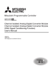
1
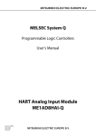
MELSEC System Q
Programmable Logic Controllers
User’s Manual
HART Analog Input Module
ME1AD8HAI-Q
Art. no.: 229753
28 01 2013
Version E
INDUSTRIAL AUTOMATION
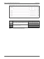
Version check
About this Manual
The texts, illustration, diagrams and examples in this manual are provided for information
purposes only. They are intended as aids to help explain the installation, operation,
programming and use of the programmable logic controllers of
the MELSEC System Q.
If you have any questions about the installation and operation of any of the products described in this
manual please contact your local sales office or distributor (see back cover).
You can find the latest information and answers to frequently asked questions
on our website at www.mitsubishi-automation.com.
MITSUBISHI ELECTRIC EUROPE BV reserves the right to make changes to this manual or the technical
specifications of its products at any time without notice.
© 2009 –2013
A
B
Version
10/2009
pdp-dk
03/2010
pdp-dk
C
12/2010
pdp-dk
D
02/2012
pdp-dk
E
01/2013
pdp-dk
HART Analog Input Module
ME1AD8HAI-Q
User´s Manual
Art.-no.: 229753
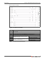
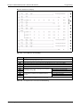
Changes / Additions / Corrections
First edition
앫 New section 3.5.25: HART device information refresh interval (Un\G191)
앫 Addition of Un\G191 to buffer memory assignment in section 3.5.1
앫 Correction in section 3.2 (Specifications, accuracy): "digital output value" was
changed to "digital output range";
"Photo coupler isolation" was changed to "Digital isolator insulation"
앫 Correction in section 3.2.2 (Accuracy)
앫 Correction in section 4.1: Subitem "A protective film is attached to the…" was
removed – Modul has no protective film.
앫 Correction in section 6.4: "…, the LED ON status…" in the first sentence was
removed.
앫 Correction on page 1-2 and corresponding on page 3-6: "…is output…" was
changed to …is triggered…" in 3 sentences.
앫 Correction on page 3-47: Meaning of the bits in buffer memory address 53 in
Fig. 3-29
앫 New chapter 5: "Intelligent Function Utility (GX Works2)"
앫 Addition of the "Intelligent function utility" in section 1.1
앫 Update of table 2-1 and the item "Supported software packages" in section 2.1
앫 Changes in section 2.2
앫 Note in table 3-8 (entry for X9)
앫 Note regarding initial settings in Fig. 6-1
Safety Guidelines
For use by qualified staff only
This manual is only intended for use by properly trained and qualified electrical technicians who are
fully acquainted with the relevant automation technology safety standards. All work with the hardware described, including system design, installation, configuration, maintenance, service and testing of the equipment, may only be performed by trained electrical technicians with approved qualifications who are fully acquainted with all the applicable automation technology safety standards
and regulations. Any operations or modifications to the hardware and/or software of our products not
specifically described in this manual may only be performed by authorised Mitsubishi Electric staff.
Proper use of the products
The programmable logic controllers of the MELSEC System Q are only intended for the specific applications explicitly described in this manual. All parameters and settings specified in this manual must
be observed. The products described have all been designed, manufactured, tested and documented
in strict compliance with the relevant safety standards. Unqualified modification of the hardware or
software or failure to observe the warnings on the products and in this manual may result in serious
personal injury and/or damage to property. Only peripherals and expansion equipment specifically
recommended and approved by Mitsubishi Electric may be used with the programmable logic controllers of the MELSEC System Q.
All and any other uses or application of the products shall be deemed to be improper.
Relevant safety regulations
All safety and accident prevention regulations relevant to your specific application must be observed
in the system design, installation, configuration, maintenance, servicing and testing of these products. The regulations listed below are particularly important in this regard. This list does not claim to
be complete, however; you are responsible for being familiar with and conforming to the regulations
applicable to you in your location.
● VDE Standards
– VDE 0100
Regulations for the erection of power installations with rated voltages below 1000 V
– VDE 0105
Operation of power installations
– VDE 0113
Electrical installations with electronic equipment
– VDE 0160
Electronic equipment for use in power installations
– VDE 0550/0551
Regulations for transformers
– VDE 0700
Safety of electrical appliances for household use and similar applications
– VDE 0860
Safety regulations for mains-powered electronic appliances and their accessories for household use and similar applications.
● Fire safety regulations
● Accident prevention regulations
– VBG Nr.4
Electrical systems and equipment
HART Analog Input Module ME1AD8HAI-Q
I
Safety warnings in this manual
In this manual warnings that are relevant for safety are identified as follows:
II
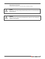
m
DANGER:
b
WARNING:
Failure to observe the safety warnings identified with this symbol can result in health and injury
hazards for the user.
Failure to observe the safety warnings identified with this symbol can result in damage to the
equipment or other property.
General safety information and precautions
The following safety precautions are intended as a general guideline for using PLC systems together
with other equipment. These precautions must always be observed in the design, installation and
operation of all control systems.
m
DANGER:
● Observe all safety and accident prevention regulations applicable to your specific application. Always disconnect all power supplies before performing installation and wiring work
or opening any of the assemblies, components and devices.
● Assemblies, components and devices must always be installed in a shockproof housing fitted
with a proper cover and fuses or circuit breakers.
● Devices with a permanent connection to the mains power supply must be integrated in the
building installations with an all-pole disconnection switch and a suitable fuse.
● Check power cables and lines connected to the equipment regularly for breaks and insulation
damage. If cable damage is found immediately disconnect the equipment and the cables
from the power supply and replace the defective cabling.
● Before using the equipment for the first time check that the power supply rating matches that
of the local mains power.
● Take appropriate steps to ensure that cable damage or core breaks in the signal lines cannot
cause undefined states in the equipment.
● You are responsible for taking the necessary precautions to ensure that programs interrupted by brownouts and power failures can be restarted properly and safely. In particular, you
must ensure that dangerous conditions cannot occur under any circumstances, even for brief
periods.
● EMERGENCY OFF facilities conforming to EN 60204/IEC 204 and VDE 0113 must remain fully
operative at all times and in all PLC operating modes. The EMERGENCY OFF facility reset
function must be designed so that it cannot ever cause an uncontrolled or undefined restart.
● You must implement both hardware and software safety precautions to prevent the possibility of undefined control system states caused by signal line cable or core breaks.
● When using modules always ensure that all electrical and mechanical specifications and
requirements are observed exactly.
HART Analog Input Module ME1AD8HAI-Q
III
IV
Contents
Contents
1
Overview
1.1
Features . . . . . . . . . . . . . . . . . . . . . . . . . . . . . . . . . . . . . . . . . . . . . . . . . . . . . . . . . . . . . . . . . . . . . . . . . 1-1
2
System Configuration
2.1
Applicable Systems. . . . . . . . . . . . . . . . . . . . . . . . . . . . . . . . . . . . . . . . . . . . . . . . . . . . . . . . . . . . . . . 2-1
2.2
How to Check the Function Version and Serial No. of the Modules . . . . . . . . . . . . . . . . . 2-3
3
Detailed Description of the Module
3.1
Part Names. . . . . . . . . . . . . . . . . . . . . . . . . . . . . . . . . . . . . . . . . . . . . . . . . . . . . . . . . . . . . . . . . . . . . . . 3-1
3.1.1
3.2
3.3
3.4
3.5
Signal Layout of the Terminal Block . . . . . . . . . . . . . . . . . . . . . . . . . . . . . . . . . . . . . . 3-2
Specifications . . . . . . . . . . . . . . . . . . . . . . . . . . . . . . . . . . . . . . . . . . . . . . . . . . . . . . . . . . . . . . . . . . . . 3-3
3.2.1
I/O conversion characteristic . . . . . . . . . . . . . . . . . . . . . . . . . . . . . . . . . . . . . . . . . . . . . 3-4
3.2.2
Accuracy . . . . . . . . . . . . . . . . . . . . . . . . . . . . . . . . . . . . . . . . . . . . . . . . . . . . . . . . . . . . . . . . 3-4
3.2.3
External Dimensions . . . . . . . . . . . . . . . . . . . . . . . . . . . . . . . . . . . . . . . . . . . . . . . . . . . . 3-5
Functions of the HART Analog Input Module . . . . . . . . . . . . . . . . . . . . . . . . . . . . . . . . . . . . . . 3-6
3.3.1
A/D conversion methods . . . . . . . . . . . . . . . . . . . . . . . . . . . . . . . . . . . . . . . . . . . . . . . . 3-7
3.3.2
Maximum and minimum values hold function . . . . . . . . . . . . . . . . . . . . . . . . . . . . 3-9
3.3.3
Input signal error detection function . . . . . . . . . . . . . . . . . . . . . . . . . . . . . . . . . . . . 3-10
3.3.4
Warning output function . . . . . . . . . . . . . . . . . . . . . . . . . . . . . . . . . . . . . . . . . . . . . . . 3-11
3.3.5
Scaling Function. . . . . . . . . . . . . . . . . . . . . . . . . . . . . . . . . . . . . . . . . . . . . . . . . . . . . . . . 3-15
3.3.6
HART Master Function . . . . . . . . . . . . . . . . . . . . . . . . . . . . . . . . . . . . . . . . . . . . . . . . . . 3-16
I/O Signals for the Programmable Controller CPU. . . . . . . . . . . . . . . . . . . . . . . . . . . . . . . . . 3-18
3.4.1
List of I/O signals . . . . . . . . . . . . . . . . . . . . . . . . . . . . . . . . . . . . . . . . . . . . . . . . . . . . . . . 3-18
3.4.2
Details of I/O signals . . . . . . . . . . . . . . . . . . . . . . . . . . . . . . . . . . . . . . . . . . . . . . . . . . . . 3-19
Buffer Memory . . . . . . . . . . . . . . . . . . . . . . . . . . . . . . . . . . . . . . . . . . . . . . . . . . . . . . . . . . . . . . . . . . 3-23
3.5.1
Buffer memory assignment . . . . . . . . . . . . . . . . . . . . . . . . . . . . . . . . . . . . . . . . . . . . . 3-24
3.5.2
A/D conversion enable/disable setting (Un\G0) . . . . . . . . . . . . . . . . . . . . . . . . . . 3-40
3.5.3
CHl Average time/Average number of times/Moving average/
Time constant settings (Un\G1 to Un\G8) . . . . . . . . . . . . . . . . . . . . . . . . . . . . . . . . 3-40
3.5.4
A/D conversion completed flag (Un\G10) . . . . . . . . . . . . . . . . . . . . . . . . . . . . . . . . 3-41
3.5.5
CHl digital output value (Un\G11 to Un\G18) . . . . . . . . . . . . . . . . . . . . . . . . . . . . 3-41
3.5.6
Write data error code (Un\G19). . . . . . . . . . . . . . . . . . . . . . . . . . . . . . . . . . . . . . . . . . 3-42
HART Analog Input Module ME1AD8HAI-Q
V
Contents
Setting range (Un\G20, Un\G21). . . . . . . . . . . . . . . . . . . . . . . . . . . . . . . . . . . . . . . . . 3-42
3.5.8
Averaging process specification (Un\G24, Un\G25). . . . . . . . . . . . . . . . . . . . . . . 3-43
3.5.9
CHl maximum value/minimum value storage area (Un\G30 to Un\G45). . . 3-44
3.5.10
Input signal error detection setting (Un\G47) . . . . . . . . . . . . . . . . . . . . . . . . . . . . 3-44
3.5.11
Warning output settings (Un\G48) . . . . . . . . . . . . . . . . . . . . . . . . . . . . . . . . . . . . . . 3-45
3.5.12
Input signal error detection flag (Un\G49) . . . . . . . . . . . . . . . . . . . . . . . . . . . . . . . 3-46
3.5.13
Warning output flag (Un\G50, Un\G51) . . . . . . . . . . . . . . . . . . . . . . . . . . . . . . . . . . 3-47
3.5.14
Scaling enable/disable setting (Un\G53) . . . . . . . . . . . . . . . . . . . . . . . . . . . . . . . . . 3-47
3.5.15
CHl scaling value storage area (Un\G54 to Un\G61) . . . . . . . . . . . . . . . . . . . . . . 3-48
3.5.16
CHl scaling upper/lower limit value (Un\G62 to Un\G77) . . . . . . . . . . . . . . . . . 3-48
3.5.17
CHl process alarm upper/lower limit value (Un\G86 to Un\G117) . . . . . . . . . 3-48
3.5.18
CHl rate alarm warning detection period (Un\G118 to Un\G125) . . . . . . . . . 3-49
3.5.19
CHl rate alarm upper/lower limit value (Un\G126 to Un\G141). . . . . . . . . . . . 3-50
3.5.20
CHl input signal error detection setting value (Un\G142 to Un\G149) . . . . . 3-50
3.5.21
HART enable (Un\G160). . . . . . . . . . . . . . . . . . . . . . . . . . . . . . . . . . . . . . . . . . . . . . . . . 3-51
3.5.22
HART scan list (Un\G161). . . . . . . . . . . . . . . . . . . . . . . . . . . . . . . . . . . . . . . . . . . . . . . . 3-51
3.5.23
HART Cycle Time (Un\G162 to Un\G164). . . . . . . . . . . . . . . . . . . . . . . . . . . . . . . . . 3-52
3.5.24
HART Maximum Retries (Un\G176 to Un\G183) . . . . . . . . . . . . . . . . . . . . . . . . . . 3-52
3.5.25
HART device information refresh interval (Un\G191) . . . . . . . . . . . . . . . . . . . . . 3-52
3.5.26
HART Field Device Status (Un\G240, Un\G252, Un\G264...) . . . . . . . . . . . . . . . 3-53
3.5.27
Extended HART Field Device Status (Un\G241, Un\G253, Un\G265...) . . . . . 3-54
3.5.28
Device Variable Status (Un\G242 & Un\G243, Un\G254 & Un\G255...) . . . . . 3-55
3.5.29
HART Process Variables (Un\G244 to Un\G251, Un\G256 to Un\G263...) . . . 3-56
3.5.30
HART Command Request (Un\G352 to Un\G483) . . . . . . . . . . . . . . . . . . . . . . . . 3-57
3.5.31
HART Command Answer (Un\G496 to Un\G627) . . . . . . . . . . . . . . . . . . . . . . . . . 3-59
3.5.32
Information about HART device (Un\G896 to Un\G966,
Un\G968 to Un\G1038...) . . . . . . . . . . . . . . . . . . . . . . . . . . . . . . . . . . . . . . . . . . . . . . . . 3-60
4
Setup and Procedures before Operation
4.1
Handling Precautions. . . . . . . . . . . . . . . . . . . . . . . . . . . . . . . . . . . . . . . . . . . . . . . . . . . . . . . . . . . . . 4-1
4.2
Setup and Procedures before Operation . . . . . . . . . . . . . . . . . . . . . . . . . . . . . . . . . . . . . . . . . . 4-2
4.3
Installation of the Module . . . . . . . . . . . . . . . . . . . . . . . . . . . . . . . . . . . . . . . . . . . . . . . . . . . . . . . . 4-3
4.4
Wiring . . . . . . . . . . . . . . . . . . . . . . . . . . . . . . . . . . . . . . . . . . . . . . . . . . . . . . . . . . . . . . . . . . . . . . . . . . . 4-4
4.5
4.6
VI
3.5.7
4.4.1
Wiring precautions . . . . . . . . . . . . . . . . . . . . . . . . . . . . . . . . . . . . . . . . . . . . . . . . . . . . . . 4-4
4.4.2
External wiring . . . . . . . . . . . . . . . . . . . . . . . . . . . . . . . . . . . . . . . . . . . . . . . . . . . . . . . . . . 4-4
PLC Parameter Setting . . . . . . . . . . . . . . . . . . . . . . . . . . . . . . . . . . . . . . . . . . . . . . . . . . . . . . . . . . . . 4-9
4.5.1
I/O assignment . . . . . . . . . . . . . . . . . . . . . . . . . . . . . . . . . . . . . . . . . . . . . . . . . . . . . . . . . . 4-9
4.5.2
Intelligent function module switch settings. . . . . . . . . . . . . . . . . . . . . . . . . . . . . . 4-10
Setting of the HART Devices . . . . . . . . . . . . . . . . . . . . . . . . . . . . . . . . . . . . . . . . . . . . . . . . . . . . . 4-11
Contents
5
Intelligent Function Utility (GX Works2)
5.1
Addition of a new Module to the Project . . . . . . . . . . . . . . . . . . . . . . . . . . . . . . . . . . . . . . . . . . 5-1
5.2
Switch Setting. . . . . . . . . . . . . . . . . . . . . . . . . . . . . . . . . . . . . . . . . . . . . . . . . . . . . . . . . . . . . . . . . . . . 5-3
5.3
Parameter Setting . . . . . . . . . . . . . . . . . . . . . . . . . . . . . . . . . . . . . . . . . . . . . . . . . . . . . . . . . . . . . . . . 5-5
5.4
Auto Refresh Settings. . . . . . . . . . . . . . . . . . . . . . . . . . . . . . . . . . . . . . . . . . . . . . . . . . . . . . . . . . . . . 5-7
5.5
Writing the Intelligent Function Module Settings to the PLC . . . . . . . . . . . . . . . . . . . . . . . 5-8
6
Programming
6.1
Programming Procedure . . . . . . . . . . . . . . . . . . . . . . . . . . . . . . . . . . . . . . . . . . . . . . . . . . . . . . . . . 6-1
6.2
Example 1: ME1AD8HAI-Q combined with PLC CPU. . . . . . . . . . . . . . . . . . . . . . . . . . . . . . . . 6-2
6.3
6.2.1
Before creating a program . . . . . . . . . . . . . . . . . . . . . . . . . . . . . . . . . . . . . . . . . . . . . . . 6-3
6.2.2
Program. . . . . . . . . . . . . . . . . . . . . . . . . . . . . . . . . . . . . . . . . . . . . . . . . . . . . . . . . . . . . . . . . 6-4
Example 2: ME1AD8HAI-Q used in Remote I/O Network. . . . . . . . . . . . . . . . . . . . . . . . . . . . 6-9
6.3.1
Before creating a program . . . . . . . . . . . . . . . . . . . . . . . . . . . . . . . . . . . . . . . . . . . . . . 6-10
6.3.2
Network Parameter and Program . . . . . . . . . . . . . . . . . . . . . . . . . . . . . . . . . . . . . . . 6-12
7
Troubleshooting
7.1
Error Code List. . . . . . . . . . . . . . . . . . . . . . . . . . . . . . . . . . . . . . . . . . . . . . . . . . . . . . . . . . . . . . . . . . . . 7-1
7.2
Troubleshooting using the LEDs of the Module . . . . . . . . . . . . . . . . . . . . . . . . . . . . . . . . . . . . 7-3
7.3
7.2.1
When the "RUN" LED is flashing or turned off . . . . . . . . . . . . . . . . . . . . . . . . . . . . . 7-3
7.2.2
When the "ERR." LED is on or flashing. . . . . . . . . . . . . . . . . . . . . . . . . . . . . . . . . . . . . 7-3
7.2.3
When the "ALM" LED is on or flashing . . . . . . . . . . . . . . . . . . . . . . . . . . . . . . . . . . . . 7-3
When the digital output values cannot be read . . . . . . . . . . . . . . . . . . . . . . . . . . . . . . . . . . . . 7-4
7.3.1
7.4
When A/D conversion completed flag does not turn ON . . . . . . . . . . . . . . . . . . 7-4
Checking the Analog Input Module Status. . . . . . . . . . . . . . . . . . . . . . . . . . . . . . . . . . . . . . . . . 7-5
Index
HART Analog Input Module ME1AD8HAI-Q
VII
Contents
VIII
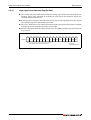
Features
1
Overview
Overview
This User's Manual describes the specifications, handling and programming methods for the HART
analog input module ME1AD8HAI-Q (hereinafter referred to as the ME1AD8HAI-Q) which is used with
the CPU modules of the MELSEC System Q. The ME1AD8HAI-Q is exclusively used for current input.
1.1
Features
Multi-channel analog input is available.
By using a single ME1AD8HAI-Q, analog current inputs of 8 points (8 channels) are available. Standard
analog input devices with 4 to 20 mA or 0 to 20 mA range can be mixed with HART devices. The analog
input range is selectable by the intelligent function module switch setting in GX(IEC) Developer. 2wire or 4-wire analog transmitters can be connected.
HART master function
The ME1AD8HAI-Q can communicate with up to eight HART-enabled devices. (One HART device connected to each channel.) HART* is a bi-directional industrial field communication protocol used to
communicate between intelligent field instruments and host systems.
For this communication no additional wiring is required. Additional device information is communicated using a digital signal that is superimposed on the analog signal. The digital signal contains information from and to the device including device configuration or re-configuration, device status, diagnostics, additional measured or calculated values, etc.
The ME1AD8HAI-Q can operate as a HART master with protocol revision 6.
* HART stands for Highway Addressable Remote Transducer. Fore more information about the HART protocol please refer to
section 3.3.6.
FDT/DTM function support
The FDT/DTM can be used for setting and monitoring the HART devices.To use this function, the HART
device must have DeviceDTM.
Power supply to 2-wire transmitter
The ME1AD8HAI-Q supplies power to the connected 2-wire transmitters.
Module protection provided by short-circuit protection circuit
If an excessive current flows into the module due to a short circuit of the wiring, the short-circuit protection circuit limits the current, thus protecting the module.
High accuracy
The accuracy is as high as ±0.15 % over the specified operating temperature range for the MELSEC
System Q.
HART Analog Input Module ME1AD8HAI-Q
1–1
Overview
Features
Changing the input range
The input range (4 to 20 mA or 0 to 20 mA) can easily be set from the GX (IEC) Developer.
A/D conversion system
There are the following five A/D conversion systems.
● Sampling processing
Analog input values are converted into digital values one by one on a channel basis and the digital
output value is triggered at every conversion.
● Averaging processing
– Time averaging
A/D conversion is averaged in terms of time on a channel basis and a digital average value is
output.
– Count averaging
A/D conversion is averaged in terms of count on a channel basis and a digital average value
is output.
– Move averaging
The specified number of digital output values measured per sampling time are averaged.
● Primary delay filter
A digital output value is smoothed according to the preset time constant.
Refer to section 3.3.1 for the details of the A/D conversion system.
Input signal error detection function
A current outside the setting range can be detected.
Warning output
There are the following two warning outputs.
● Process alarm
A warning is triggered if a digital output value falls outside the setting range.
● Rate alarm
A warning is triggered if the varying rate of a digital output value falls outside the preset varying
rate range.
Scaling function
A/D conversion values can be converted to percentage values (%) in the preset range and be
loaded into the buffer memory. This function can reduce the time required for programming.
(Refer to section 3.3.5)
Easy settings using the "Intelligent function utility"
The "Intelligent function utility" is not a required item, however, it is useful for on-screen setting of the
intelligent function module parameters (initial setting/auto refresh setting).*
* The "Intelligent function utility" is supported by the ME1AD8HAI-Q if the first 5 digits of the serial number are "14102" or
higher.
1–2
Applicable Systems
System Configuration
2
System Configuration
2.1
Applicable Systems
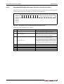
Applicable modules, base units, and No. of modules
● When mounted with a CPU module
The table below shows the CPU modules and base units applicable to the HART Analog Input Module
ME1AD8HAI-Q and quantities for each CPU model.
Depending on the combination with other modules or the number of mounted modules, power supply capacity may be insufficient. Pay attention to the power supply capacity before mounting modules, and if the power supply capacity is insufficient, change the combination of the modules.
Applicable CPU module
CPU type
CPU model
No. of
ME1AD8HAI-Q that
can be installed*1
Q00JCPU
Basic model
QCPU
Q00CPU
Q01CPU
Base unit*2
Main base unit
Extension base unit
Up to 64
Up to 64
Up to 53
—
Up to 64
Up to 16
Up to 24
Q02CPU
High
performance
model QCPU
Q02HCPU
Q06HCPU
Q12HCPU
Q25HCPU
Q02PHCPU
Process CPU
Programmable
controller CPU
Q06PHCPU
Q12PHCPU
Q25PHCPU
Redundant
CPU
Q12PRHCPU
Q25PRHCPU
Q00UJCPU
Q00UCPU
Q01UCPU
Universal
model QCPU
Q02UCPU
Up to 16
Up to 24
Up to 36
QUD(E)CPU
Q50UDEHCPU
Up to 64
Q100UDEHCPU
Safety CPU
QS001CPU
Q06CCPU-V-H01
C Controller module
Q06CCPU-V
Q06CCPU-V-B
Q12DCCPU-V
Tab. 2-1:
Applicable base units and number of mountable modules
: Applicable, : N/A
*1 Limited within the range of I/O points for the CPU module.
*2 Can be installed to any I/O slot of a base unit.
NOTE
A ME1AD8HAI-Q can not installed at the main base in a redundant system with QnPRHCPU.
HART Analog Input Module ME1AD8HAI-Q
2–1
System Configuration
Applicable Systems
● Mounting to a MELSECNET/H remote I/O station
The table below shows the network modules and base units applicable to the analog input module
ME1AD8HAI-Q and quantities for each network module model.
Depending on the combination with other modules or the number of mounted modules, power supply capacity may be insufficient. Pay attention to the power supply capacity before mounting modules, and if the power supply capacity is insufficient, change the combination of the modules.
Applicable network module
No. of ME1AD8HAI-Q that
can be installed*1
Base unit*2
Main base unit
of remote I/O station
Extension base unit
of remote I/O station
QJ72LP25-25
QJ72LP25G
Up to 64
QJ72LP25GE
QJ72BR15
Tab. 2-2:
Applicable base units and number of mountable modules in a MELSECNET/H remote I/O
station
: Applicable, : N/A
*1 Limited within the range of I/O points for the network module.
*2 Can be installed to any I/O slot of a base unit.
NOTE
The Basic model QCPU or C Controller module cannot create the MELSECNET/H remote I/O network.
Support of the multiple CPU system
The function version of the HART analog input module supports the multiple CPU system. When
using the ME1AD8HAI-Q in a multiple CPU system, refer to the following manual first.
– QCPU User's Manual (Multiple CPU System)
● Intelligent function module parameters
Write intelligent function module parameters to only the control CPU of the ME1AD8HAI-Q.
Compatibility with online module change
The ME1AD8HAI-Q does not support online module change.
Supported software packages
For setting the PLC parameters for a system containing the ME1AD8HAI-Q and programming, the
software packages GX Developer, GX IEC Developer and GX Works2 can be used.
In addition, the Intelligent Function Utility of GX Works2 can be used to set the intelligent function
module parameters (initial settings/auto refresh settings) of the ME1AD8HAI-Q.
Depending on the CPU module used, a certain version of the software is needed since newly CPU
modules are not supported by previous versions.
NOTE
2–2
Please check whether the mounted CPU module is supported or not by your version of the programming software.
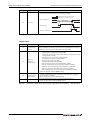
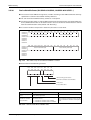
How to Check the Function Version and Serial No. of the Modules
2.2
System Configuration
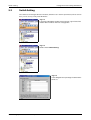
How to Check the Function Version and Serial No. of the
Modules
Using the programming software GX Developer, GX IEC Developer or GX Works2, the serial No. and
the function version can be checked while the PLC is operating.
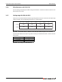
From the Diagnostics menu select System Monitor and then select Product Inf. List.
Serial number
(first 5 digits)
Fig. 2-1:
NOTE
Function
version
Product Information List for a PLC with a ME1AD8HAI-Q
The serial number displayed on the product information screen of GX Developer, GX IEC Developer or GX Works2 describes the function information of the product. The function information of
the product is updated when a new function is added.
HART Analog Input Module ME1AD8HAI-Q
2–3
System Configuration
2–4
How to Check the Function Version and Serial No. of the Modules
Part Names
Detailed Description of the Module
3
Detailed Description of the Module
3.1
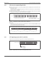
Part Names
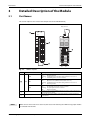
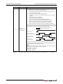
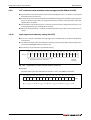
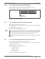
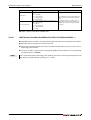
This section explains the names of the components for the ME1AD8HAI-Q.
Bottom view
�
ME1AD8HAI-Q
ALM
RUN
ERR.
2Wire
(4Wire)
C + (NC)
H – (In)
1
C + (NC)
1
2
3
H – (In)
2
C + (NC)
4
H – (In)
3
C + (NC)
6
H – (In)
4
C + (NC)
8
H – (In)
5
C + (NC)
10
H – (In)
6
C + (NC)
12
H – (In)
7
C + (NC)
14
7
0V
9
0V
H – (In)
8
IN
24VDC
�
5
�
11
13
15
16
17
18
A/D
0~20mA
�
Fig. 3-1:
No.
Name
�
LEDs
Description
RUN
Displays the operating status of the ME1AD8HAI-Q.
On:
Normal operation
Flashing: Intelligent function module setting switch 4 is not set to "0".
Off:
A watchdog timer error has occurred.
ERR.
Displays the error status of the ME1AD8HAI-Q.
On:
Operation error (HART communication error etc.)
Flashing: Intelligent function module setting switch 5 is not set to "0".
Off:
Normal operation
ALM
Indicates the warning status of the ME1AD8HAI-Q.
On:
An alarm (process alarm etc.) has occurred.
Flashing: An input signal error has occurred.
Off:
Normal operation
�
Detachable terminal block
Used for connection of the HART input devices (slaves), analog input devices
and external power supply.
�
0V/FG connector
Used for FG connection and for connection with the ‘- (minus)’ terminal of
4 wire devices.
Tab. 3-1:
NOTE
Names of parts
Description of the LEDs and the terminal blocks of the ME1AD8HAI-Q
When two or more errors have occurred, the latest error found by the HART analog input module
is indicated with the LED.
HART Analog Input Module ME1AD8HAI-Q
3–1
Detailed Description of the Module
3.1.1
Part Names
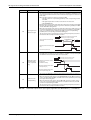
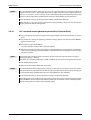
Signal Layout of the Terminal Block
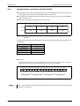
Tab. 3-2: Signal layout for the detachable
terminal block of the ME1AD8HAI-Q
Terminal No.
1
2
3
4
5
6
7
8
9
10
11
12
13
14
15
16
17
18
Signal name
CH1
CH2
CH3
CH4
CH5
CH6
CH7
CH8
External power
supply
+ (NC)
– (In)
+ (NC)
– (In)
+ (NC)
– (In)
+ (NC)
– (In)
+ (NC)
– (In)
+ (NC)
– (In)
+ (NC)
– (In)
+ (NC)
– (In)
+ 24VDC
0V
For the wiring of the HART analog input module ME1AD8HAI-Q please refer to section 4.4.
3–2
Specifications
3.2
Detailed Description of the Module
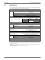
Specifications
The specifications for the ME1AD8HAI-Q are shown in the following table. For general specifications,
refer to the operation manual for the CPU module being used.
Item
Specifications
Number of analog input points
8 points (8 channels)
0 to 20 mA DC
4 to 20 mA DC
Current
Analog input
Absolute maximum input
± 30 mA
Input resistance
250
Short-circuit protection
Available
Primary filter
5 Hz (3 dB), HART signal is 1200 Hz with 1 mAP-P
Digital output
16-bit signed binary (–768 to 32767)
Analog input range
I/O characteristics, maximum resolution
0 to 20 mA
4 to 20 mA
Digital output
value
0 to 32000
625.0 nA
500.0 nA
±0.15% (±48 digit*2)
Accuracy*1 (relative to digital output range)
Cycle time
80 ms (Independent to the number of used channels)
Between the I/O terminals and
PLC power supply
Insulation
method
Photo-coupler insulation
Between analog input
channels
Non-insulated
HART modem
FSK Physical Layer, multiplexed
– Protocol Revision 6 support
– 4 Process variables support (PV, SV, TV, QV)
– FDT/DTM support
HART functions
Number of I/O occupied points
32 points (I/O assignment: Intelligent 32 points)
External wiring connection system
Applicable wire size
18-points terminal block
Refer to the HART specification for more details.
The external power supply voltage of the ME1AD8HAI-Q should be enough
for correct operation of the analog transmitter. *3 *4
Applicable solderless terminals
Voltage
External supply power
Current
Inrush current
Online module change
R1.25-3 (Solderless terminals with sleeves cannot be used.)
24 V DC (+20%, -15%); ripple, spike within 500mVP-P
0.3 A
5.5 A within 200 μs
Not supported
Internal current consumption (5 VDC)
0.32 A
Weight
0.19 kg
Tab. 3-3:
Maximum
resolution
Specifications of ME1AD8HAI-Q
*1 ME1AD8HAI-Q needs to be powered on 30 minutes prior to operation for compliance to the specification (accuracy).
*2 "digit" indicates a digital value.
*3 Use case:
For distances up to 800 m, the wire size of 0.51 mm diameter with 115 nF/km cable capacitance and 36.7 /km cable
resistance can be applied.
*4 Refer to the calculation example shown in section 4.4.2 (External wiring).
HART Analog Input Module ME1AD8HAI-Q
3–3
Detailed Description of the Module
3.2.1
Specifications
I/O conversion characteristic
The I/O conversion characteristic represents the angle formed by a straight line when the analog current signals from outside the programmable controller are converted to digital values.
Digital output value
Practical analog input range
Analog input current [mA]
Fig. 3-2:
Current input characteristics of the ME1AD8HAI-Q
쐃 Analog input range setting: 4 to 20 mA
쐇 Analog input range setting: 0 to 20 mA
NOTES
Choose the appropriate analog input range for each channel according to the specifications of the
connected analog input device.
If these ranges are exceeded, the maximum resolution and accuracy may not fall within the performance specifications. (Avoid use shown by the dotted lines in the above table.)
Do not input an analog input current of ±30 mA or more. The input elements may be damaged.
When an analog value that exceeds the range of the digital output value is entered, the digital
output value will be fixed at the maximum or minimum value (32767 resp. -768).
3.2.2
Accuracy
The reference accuracy is the accuracy relative to the digital output range.
An accuracy of ±0.15 % is maintained over the whole operating temperature range of the MELSEC System Q (0 to +55 C).
3–4
Specifications
3.2.3
Detailed Description of the Module
External Dimensions
27.4
90
22
ME1AD8HAI-Q
ALM
RUN
ERR.
2Wire
(4Wire)
1
2
3
H – (In)
2
C + (NC)
4
H – (In)
3
C + (NC)
6
H – (In)
4
C + (NC)
8
H – (In)
5
C + (NC)
10
H – (In)
6
C + (NC)
12
H – (In)
7
C + (NC)
14
H – (In)
8
IN
24VDC
5
7
98
C + (NC)
H – (In)
1
C + (NC)
9
11
13
15
16
17
18
A/D
0~20mA
10
40
0V
0V
Fig. 3-3:
Dimensions of the ME1AD8HAI-Q
(Unit: mm)
HART Analog Input Module ME1AD8HAI-Q
3–5
Detailed Description of the Module
3.3
Functions of the HART Analog Input Module
Functions of the HART Analog Input Module
Item
Function
A/D conversion
enable/disable setting
Specifies whether to enable or disable the A/D conversion for each
channel.
Reference
section
Section 3.5.2
Sampling processing
The A/D conversion for analog input values is performed successively
for each channel, and the digital output value is output upon each
conversion.
Averaging processing
– Time averaging
A/D conversion method
A/D conversion is averaged in terms of time on a channel basis and
a digital average value is output.
– Count averaging
Section 3.3.1
A/D conversion is averaged in terms of count on a channel basis
and a digital average value is output.
– Move averaging
The specified number of digital output values measured per cycle
time are averaged.
Primary delay filter
A digital output value is smoothed according to the preset time constant.
Maximum and minimum
values hold function
The maximum and minimum values of the digital output values are
retained in the module.
Section 3.3.2
Input signal error
detection function
A current outside the setting range can be detected.
Section 3.3.3
Warning output function
Process alarm
A warning is output if a digital output value falls outside the setting
range.
Rate alarm
A warning is output if the varying rate of a digital output value falls
outside the preset varying rate range.
Section 3.3.4
Scaling function
Conversion of A/D conversion values to preset percentage values and
loading into the buffer memory is available. Programming steps for the
scaling can be eliminated.
Section 3.3.5
HART Master function
HART communication support
The ME1AD8HAI-Q can communicate with up to eight HART-enabled
devices. (One HART device connected to each channel.) Communication occurs using standard instrumentation grade wire and using standard wiring and termination practices – no additional wiring is
required.
FDT/DTM function support
Using a commercially available FDT, reading/writing the HART transmitter’s parameters and monitoring the HART transmitter status are
executable via the ME1AD8HAI-Q.
Section 3.3.6
Tab. 3-4:
3–6
Functions of the ME1AD8HAI-Q
Functions of the HART Analog Input Module
3.3.1
Detailed Description of the Module
A/D conversion methods
Sampling processing
A/D conversion is performed successively for analog input values, and the converted digital output
values are stored in the buffer memory.
Averaging processing
● Time averaging
A/D conversion is made for the preset period of time, the sum of values other than the maximum
and minimum values is averaged, and the result is stored into the buffer memory.
The number of processing within the set time depends on the cycle time (Fixed to 80 ms
independently to the number of channels enabled for A/D conversion) and can be calculated
using the following formula:
Number of processings [times] = Set time [ms] /80 [ms]
Example:
Number of processings when setting 500 ms for the set time: 500/80 = 6.25 [times] 6 [times]
● Count averaging
A/D conversion is made the preset number of times, the sum of values other than the maximum
and minimum values is averaged, and the result is stored into the buffer memory.
The time required for the count-based average value to be stored into the buffer memory varies
depends on the cycle time (Fixed to 80 ms independently to the number of channels enabled for
A/D conversion) and can be calculated using the following formula:
Processing time [ms] = Set count x 80 [ms]
Example:
Processing time when setting 5 (times) for the average processing count: 5 x 80 = 400 [ms]
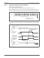
● Moving average
The specified count of digital output values imported per sampling period are averaged to find
a value, which is then stored into the buffer memory. Since average processing is performed with
data shifted per sampling, the most recent digital output value is obtainable.
A/D conversion
value
Sampling period
12000
3)
2)
4)
5)
1)
6)
7)
8)
9)
12)
10) 11)
Buffer memory
6000
First storage
Second storage
Third storage
0
A/D conversion completed flag ON
Digital output value
Time [ms]
Data transition inside buffer memory
Fig. 3-4:
First storage
Second storage
Third storage
1)+2)+3)+4)
2)+3)+4)+5)
3)+4)+5)+6)
4
4
4
Moving average processing at the preset count of 4 times
HART Analog Input Module ME1AD8HAI-Q
3–7
Detailed Description of the Module
Functions of the HART Analog Input Module
Primary delay filter
A digital value whose transient noise has been smoothed is output according to the preset time constant. The degree of smoothing varies with the time constant setting.
The relational expression of the time constant and digital output value is indicated below.
[If n = 1]
Yn = 0
[If n = 2]*
Yn = yn-1 +
t
t + TA
(yn - yn-1)
[If n 욷 3]
Yn = Yn-1 +
t
(yn - Yn-1)
t + TA
Yn: Current digital output value
Yn-1: Immediately preceding digital
output value
n:
Sampling count
TA: Time constant [s]
yn: Pre-smoothing digital output value
Yn-1: Immediately preceding presmoothing
digital output value
욼t: Cycle time (0.08)[s]
*The A/D conversion completed flag turns ON when n 욷 2.
Example 1:
Digital output value when the analog input value varies from 4 to 10 mA
The variation of the digital output value at the time constant setting of 1000 ms (1 s) is as shown below.
1000 ms (1 s) after the analog input value has reached 10 mA, the digital output value reaches 63.2 %
of the value attained when the sampling processing is selected.
12000
9
10000
8
8000
7
6000
6
4000
5
2000
4
3–8
Digital output value
0
0
1000
Elapsed time (ms)
Digital output value
Analog input value (mA)
Analog input value
10
Functions of the HART Analog Input Module
Detailed Description of the Module
Example 2:
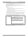
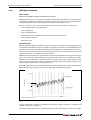
Digital output value when the variation of the analog input value has a ringing waveform
The variations of the digital output values at the time constant setting of 2000 ms (2 s), at the time
constant setting of 1000 ms (1 s), and at the moving average processing of 16 times are as shown
below.
Digital output value
(moving average processing: 16 times)
Digital output value
(time constant setting: 2000ms)
12000
9
10000
8
8000
7
6000
6
4000
5
2000
4
3.3.2
Digital output value
(time constant setting: 1000ms)
0
Digital output value
Analog input value (mA)
10
Analog input value
0
Elapsed time (ms)
Maximum and minimum values hold function
The maximum and minimum values are held in the buffer memory channel by channel.
The maximum and minimum values are cleared to 0 when the maximum value/minimum value reset
request (YD) or operating condition setting request (Y9) is turned ON, and new maximum and minimum values are stored when conversion is started.
Since the area for storing the maximum and minimum values can be rewritten with the sequence program, the maximum and minimum values within a specific period of time can be checked.
When the scaling function is enabled, values after scaling conversion are stored as the maximum and
minimum values. For the scaling function, refer to section 3.3.5
HART Analog Input Module ME1AD8HAI-Q
3–9
Detailed Description of the Module
3.3.3
Functions of the HART Analog Input Module
Input signal error detection function
If the input current rose to or above the input signal error detection upper limit value or fell to or below
the lower limit value, the input signal error detection flag (Un\G49) and input signal error detection
signal (XC) turn ON and the ALM LED flickers to indicate the error.
When the input signal error detection flag (Un\G49) turns ON for a channel, a digital output value
immediately before the error detection is held for the channel, and the A/D conversion completed
flag (Un\G10) of the corresponding channel turns OFF.
By bringing the analog input value within the setting range and then turning ON the error clear
request (YF), the input signal error detection flag (Un\G49) and input signal error detection signal (XC)
turn OFF.
When the analog input value returns to within the setting range, A/D conversion is resumed independently of whether the input signal error detection flag (Un\G49) and input signal error detection
signal (XC) are reset or not, the A/D conversion completed flag (Un\G10) of the corresponding channel turns ON again after the first updating. (The ERR. LED remains flickering.)
Analog input value
Error detection
Upper limit
value
CH1 analog
input value
Input value
normal
Lower limit
value
Time
CH1 input signal error detection flag
(Un\G49, b0)
Input signal error detection signal
(XC)
CH1 A/D conversion completed flag
(Un\G10, b0)
Error clear request (YF)
Fig. 3-5:
Input signal error detection function
This function is executed at every sampling processing. Perform the following procedure to use this
function.
– Set the input signal error detection setting value for the corresponding channel.
– Enable the A/D conversion of the corresponding channel.
– Enable the input signal error detection of the corresponding channel.
– Turn ON the operating condition setting request (Y9).
3 – 10
Functions of the HART Analog Input Module
3.3.4
Detailed Description of the Module
Warning output function
Process alarm
If the detected digital output value rose to or above the process alarm upper upper limit value or fell
to or below the process alarm lower lower limit value and entered the warning output range zone, the
warning output flag (process alarm)(Un\G50) and warning output signal (X8) turn ON and the ALM
LED is lit to indicate the warning.
A warning will be output according to the following digital output values.
Item
Digital value causing warning output
Value set in scaling enable/disable setting
(Un\G53)
Tab. 3-5:
0: Disable
CH digital output value (Un\G11 to Un\G18)
1: Enable
CH scaling value (Un\G54 to Un\G61)
The source for the warning depends on the setting in the buffer memory address Un\G53
The warning output signal (X8) turns OFF only when all channels return to within the setting range.
Digital output value
Warning
occurrence
Upper upper
limit value
Upper lower
limit value
Warning output range
Warning output range outside
Included
Warning
occurrence
Warning cancel
CH1 digital output
value
Warning cancel
Warning cancel
Lower upper
limit value CH2 digital
output value
Lower lower
limit value
Warning
occurrence
Time
CH1 process alarm upper limit value
(Un\G50,b0)
CH1 process alarm lower limit value
(Un\G50,b1)
CH2 process alarm upper limit value
(Un\G50,b2)
Warning output signal (X8)
Fig. 3-6:
Warning output function (process alarm)
When time or count averaging is specified, this function is executed at intervals of the preset averaging time or averaging count. When any other A/D conversion system (sampling processing, moving
average, primary delay filter) is specified, this function is executed at intervals of the cycle time.
To use the scaling function, be sure to consider the scaling conversion before setting the CH process
alarm upper/lower limit value.
HART Analog Input Module ME1AD8HAI-Q
3 – 11
Detailed Description of the Module
Functions of the HART Analog Input Module
Rate alarm
If the range of change in the digital output value sampled at intervals of the rate alarm warning detection period is equal to or greater than the rate alarm upper limit value or is equal to or less than the rate
alarm lower limit value, the warning output flag (rate alarm) (Un\G51) and warning output signal (X8)
turn ON and the ALM LED is lit to indicate the warning of the rate alarm.
If, after the output of the warning, the rate fell below the rate alarm upper limit value or rose above the
rate alarm lower limit value and returned to within the setting range, "0" is stored into the bit position
corresponding to the channel number of the warning output flag (rate alarm) (Un\G51). The warning
output signal (X8) turns OFF only when all channels return to within the setting range
Digital output value
Rate alarm
warning detection
period
CH1 digital
output value
CH2 digital
output value
Varying rate (%) of
digital output value
Rate alarm
warning detection
period
Varying rate of
CH2 digital
output value
Time
Rate alarm
upper limit
value
Rate alarm
lower limit
value
Varying rate of
CH1 digital
output value
Time
CH1 rate alarm upper limit value
(Un\G51,b0)
CH1 rate alarm lower limit value
(Un\G51,b1)
CH2 rate alarm lower limit value
(Un\G51,b2)
Warning output signal (X8)
Fig. 3-7:
Warning output function (rate alarm)
Set the rate alarm upper limit value/lower limit value in 0.1 %/s increments relative to the maximum
value (32000) of the digital output value. The setting range is -32768 to 32767 (-3276.8 % to 3276.7 %).
The setting range of the rate alarm warning detection period is 80 to 5000 ms. When the period is set
to 5000 ms, the digital values are compared at intervals of 5 seconds to detect the varying rate.
3 – 12
Functions of the HART Analog Input Module
Detailed Description of the Module
The rate alarm is judged by converting the rate alarm upper/lower limit value into the digit value per
rate alarm warning detection period. The expression for the value used to make judgment per rate
alarm warning detection period is as follows:
Value used to make judgment per rate alarm warning detection period [digit] =
rate alarm upper limit value or lower limit value x 0.001 x maximum value of the digital output value
x rate alarm warning detection period 앦 1000
● Example
The following is set for channel 1:
– Upper limit value of change rate: 30 % per second (300 is stored in buffer memory)
– Maximum digital output value: 32000
– Rate alarm warning detection period: 80 ms
The value [digit] used at every rate alarm warning detection period can be calculated as follows:
300 x 0.001 x 32000 x 80 / 1000 = 768 (digit)
Therefore, the current value is compared with the previous value every 80 ms in channel 1, and
whether a difference of 768 (digit) or more is identified between them or not is determined.
The rate alarm is useful to watch the varying rate of the digital output value in a limited range.
● Example of setting the rate alarm upper limit value/lower limit value when it is desired to watch
that the digital output value increases within the specified range
Varying rate (%) of
digital output value
+30%
Rate alarm upper limit value
+20%
Rate alarm lower limit value
0
Time
Fig. 3-8:
Rate alarm for increasing values
HART Analog Input Module ME1AD8HAI-Q
3 – 13
Detailed Description of the Module
Functions of the HART Analog Input Module
● Example of setting the rate alarm upper limit value/lower limit value when it is desired to watch
that the digital output value decreases within the specified range
Varying rate (%) of
digital output value
0
Rate alarm upper limit value
-20%
-30%
Rate alarm lower limit value
Time
Fig. 3-9:
Rate alarm for decreasing values
● Example of setting the rate alarm upper limit value/lower limit value when it is desired to watch
that the digital output value increases/decreases within the specified range
Varying rate (%) of
digital output value
Rate alarm upper limit value
+10%
0
-10%
Rate alarm lower limit value
Time
Fig. 3-10: Rate alarm for increasing and decreasing values
3 – 14
Functions of the HART Analog Input Module
3.3.5
Detailed Description of the Module
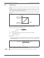
Scaling Function
With this function, A/D conversion values are converted to rate values and loaded into the buffer
memory.
A digital value stored in CH digital output value (Un\G11 to Un\G18) is converted to a value in the
range set by CH scaling upper/lower limit value (Un\G62 to Un\G77). The converted value is stored
in CH scaling value storage area (Un\G54 to Un\G61).
The scaling function is used for processed values when using the averaging processing or primary
delay filter.
Digital output value
Scaling
upper limit value
Analig input
current (mA)
Scaling
lower limit value
Fig. 3-11: Scaling function for input range settings 0 to 20 mA and 4 to 20 mA
How to calculate a scaling value is explained below.
Scaling value =
DX × (SH-SL)
+ SL
Dmax
Dx:
Digital output value
DMax:
The maximum digital output value in the input range being used (32000)
SH :
Scaling upper limit value
SL :
Scaling lower limit value
● Example
Using the input range from 4 to 20 mA, 14 mA input result in a digital output value (DX) of 20000.
With a scaling upper limit value (SH) of 2000 and a scaling lower limit value (SL) of 500 the scaling
value for 14 mA input is:
Scaling value =
20000 x (2000 - 500)
+ 500
32000
= 1437.5....
= 1437
Fig. 3-12: Example for the calculation of the scaling value
NOTE
In the calculation of the scaling value, the digits following the decimal point are omitted.
HART Analog Input Module ME1AD8HAI-Q
3 – 15
Detailed Description of the Module
3.3.6
Functions of the HART Analog Input Module
HART Master Function
What is HART?
HART stands for Highway Addressable Remote Transducer.
HART Communication is a bi-directional industrial field communication protocol used to communicate between intelligent field instruments and host systems. A host system can be a handheld device,
a Distributed Control System, Asset Management System, Safety System or a PLC.
There are several reasons to have a host communicate with a field instrument. These include:
– Device Configuration or re-configuration
– Device Diagnostics
– Device Troubleshooting
– Reading the values of additional measurements provided by the device
– Device Health and Status
– And much more!
How HART Works
When using the ME1AD8HAI-Q, HART communication takes place between the analog input module
and an HART-enabled field device, for example a temperature transmitter. The ME1AD8HAI-Q can
communicate with up to eight HART-enabled devices. (One HART device connected to each channel.)
Communication occurs using standard instrumentation grade wire and using standard wiring and
termination practices – no additional wiring is required.
HART provides two simultaneous communication channels: the 4 to 20 mA analog signal and a digital
signal. The 4 to 20 mA signal communicates the primary measured value fast robust and reliable.
Additional device information is communicated using a digital signal that is superimposed on the
analog signal. The digital signal contains information from the device including device status, diagnostics, additional measured or calculated values, etc.
The HART protocol makes use of the Bell 202 Frequency Shift Keying (FSK) standard to superimpose
digital communication signals at a low level on top of the 4 to 20 mA analog signal.
20 mA
Input current
Digital signal
앧0.5 mA
"1"
"0"
"0"
"1"
"1"
"0"
"1"
"1"
"0"
Analog signal
4 mA
Note: Drawing not to scale
Time
Fig. 3-13: Digital communication is superimposed on the analog signal
A digital signal with a frequency of 2200 Hz is interpreted as logical "0", whereas a frequency of
1200 Hz is interpreted as logical "1".
The HART protocol communicates without interrupting the 4 to 20 mA signal and allows a host appli-
3 – 16
Functions of the HART Analog Input Module
Detailed Description of the Module
cation (in this case the ME1AD8HAI-Q) to get two or more digital updates per second from a field
device. As the digital FSK signal is phase continuous, there is no interference with the analog 4 to
20 mA signal.
HART is a master/slave protocol which means that a field (slave) device only speaks when spoken to
by the ME1AD8HAI-Q (master). This is done by commands send by the ME1AD8HAI-Q. Codes vary by
manufacturer/device.
Examples for commands:
– Set Primary Variable Units
– Set Upper Range
– Set Lower Range
– Set Damping Value
– Set Tag
– Set Date
– Set Descriptor
– Perform Loop Test - Force loop current to specific value
– Initiate Self Test - Start device self test
– Get More Status Available Information
NOTE
The supported commands are depended on the specification of the HART transmitter.
The ME1AD8HAI-Q can operate as a HART master with protocol revision 6.
HART Data
The following list is only a brief overview of the data transmitted via the HART protocol. Fore more
information please refer to the description of the buffer memory (Section 3.5.1).
● Digital data: 35 to 40 valuable data items standard in every HART device
● Device identification: device tag, supplier, device type and revision, device serial number
● Calibration data: upper and lower range values, upper and lower sensor limits, PV damping, last
calibration date
● Process variables: primary variable plus secondary measurements and multivariable parameters
● Status/diagnostic alerts: device malfunction, configuration change, power fail restart, loop current fixed or saturated, primary or secondary variable out of limits, communication error etc.
More information
This short overview about the HART protocol is only a extract of the information provided on the website of the HART Communication Foundation. You can find much more information about HART and
answers to frequently asked questions on their website at www.hartcomm2.org.
FDT/DTM function support
Support of FDT/DTM function.
Using a commercially available FDT, reading/writing the HART transmitter’s parameters and monitoring the HART transmitter status are executable via the ME1AD8HAI-Q.
Refer to section 4.6 (Setting of the HART Devices) for more details about the FDT/DTM system
structure.
HART Analog Input Module ME1AD8HAI-Q
3 – 17
Detailed Description of the Module
I/O Signals for the Programmable Controller CPU
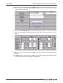
3.4
I/O Signals for the Programmable Controller CPU
3.4.1
List of I/O signals
Note that I/O numbers (X/Y) shown in this chapter and thereafter are the values when the start I/O
number for the ME1AD8HAI-Q is set to 0 (i.e. the module is mounted to the I/O slot 0 of the main base
unit).
Signal direction CPU Module ME1AD8HAI-Q
Device No. (Input)
Signal name
X0
Module ready
X1
X2
X3
Use prohibited
HART device variables access flag
X4
X5
X6
Use prohibited
Warning output signal
X9
Operating condition setting completed flag
Y3
HART device variables access request
Y5
Y6
Use prohibited
Use prohibited
Y8
Y9
Operating condition setting request
YA
YB
Use prohibited
Input signal error detection signal
YC
XD
Maximum value/minimum value
reset completed flag
YD
Maximum value/minimum value
reset request
XE
A/D conversion completed flag
YE
Use prohibited
XF
Error flag
YF
Error clear request
Use prohibited
Y10
to
Y1F
Use prohibited
Tab. 3-6:
3 – 18
Use prohibited
Y2
XC
X10
to
X1F
NOTE
Y1
Y7
X8
XB
Y0
Y4
X7
XA
Signal direction CPU Module ME1AD8HAI-Q
Device No. (Output) Signal name
I/O signals of the ME1AD8HAI-Q
The "Use prohibited" signals cannot be used by the user since they are for system use only.
If these are turned ON/OFF by the sequence program, the performance of the HART analog input
module cannot be guaranteed.
I/O Signals for the Programmable Controller CPU
3.4.2
Detailed Description of the Module
Details of I/O signals
Input signals
Device No.
X0
Signal Name
Description
Module ready
When the programmable controller CPU is powered on or reset, this signal turns
on once the preparation for A/D conversion has been completed. Afterwards A/D
conversion processing is performed.
When the analog input module has a watchdog timer error*1, "Module ready" (X0)
turns OFF (In this case A/D conversion processing is not performed.)
X3
X8
HART device variables access flag
Warning output
signal
This signal turns ON while the HART device variables and device variable status
(Buffer Memory Un\G240 to Un\G335) are accessed for update.
If data consistency for the HART device variables and device variables status is
required, do not read the variables while this signal is ON and set the Y3 signal
when reading the variables.
The Warning output signal (X8) turns ON at detection of a process alarm or rate
alarm.
Process alarm
– This signal turns ON when the digital output value falls outside the setting
range set to the process alarm upper/lower limit values (Un\G86 to Un\G117)
on any of the channels enabled for A/D conversion after the process alarm
function has been made valid.
– As soon as the digital output values return to within the setting ranges on all
channels enabled for A/D conversion, this signal turns OFF automatically and
the ALM LED is also extinguished.
Rate alarm
– This signal turns ON when the varying rate of the digital output value falls
outside the varying rate range set to the rate alarm upper/lower limit values
(Un\G126 to Un\G141) on any of the channels enabled for A/D conversion
after the rate alarm function has been made valid.
– As soon as the varying rates of the digital output values return to within the
preset varying ranges on all channels enabled for A/D conversion, this signal
turns OFF automatically and the ALM LED is also extinguished.
Performed by the HART Analog Input module
Performed by the sequence program
Warning output flag
(Un\G50, Un\G51)
0
Warning occurrence
(Process alarm, rate alarm)
0
Warning output signal (X8)
Tab. 3-7:
Detailed description of the input signals (Signal direction ME1AD8HAI-Q CPU Module)
*1 A watchdog timer error occurs when the program calculations are not completed within the scheduled time due to
malfunctions of the analog input module hardware.
When a watchdog timer error occurs, the RUN LED of the analog input module turns off.
HART Analog Input Module ME1AD8HAI-Q
3 – 19
Detailed Description of the Module
Device No.
Signal Name
I/O Signals for the Programmable Controller CPU
Description
This signal is used as an interlock condition to turn ON/OFF the Operating condition setting request (Y9) when any of the following settings has been changed.
– A/D conversion enable/disable setting (Un\G0)
– CH Average time/Average number of times/Moving average/Time constant settings (Un\G1 to Un\G8)
– Averaging process specification (Un\G24, Un\G25)
– Input signal error detection extended/input signal error detection setting
(Un\G47)
– Warning output settings (Un\G48)
– Scaling enable/disable setting(Un\G53)
– CH scaling upper/lower limit value (Un\G62 to Un\G77)
– CH process alarm upper/lower limit value (Un\G86 to Un\G117)
– CH rate alarm warning detection period (Un\G118 to Un\G125)
– CH rate alarm upper/lower limit value (Un\G126 to Un\G141)
– CH input signal error detection setting value (Un\G142 to Un\G149)
When the operating condition setting completed flag (X9) is OFF, A/D conversion
processing is not performed. The operating condition setting completed flag (X9)
turns OFF when operating condition setting request (Y9) is ON.
X9
Performed by the HART Analog Input Module
Performed by the sequence program
Operating
condition setting
completed flag
Module ready (X0)
Operating condition
setting completed flag (X9)
Operating condition
change request (Y9)
A/D conversion
completed flag (XE)
Digital output values are cleared immediately after the Operating condition
change request (Y9) turns ON. Therefore, check the status of the A/D conversion
completed flag before reading digital outputs.
NOTE
If the “Intelligent function utility” is used for configuration, the settings made with
this function are restored under the following conditions:
– CPU Power off CPU RUN
– CPU RESET CPU RUN
– CPU STOP CPU RUN
Tab. 3-8:
3 – 20
Detailed description of the input signals (Signal direction ME1AD8HAI-Q CPU Module)
I/O Signals for the Programmable Controller CPU
Device No.
XC
Signal Name
Input signal error
detection signal
Detailed Description of the Module
Description
This signal turns ON when the analog input value falls outside the setting range
set to the Input signal error detection setting value (Un\G142 to Un\G149) on any
of the channels enabled for A/D conversion after the Input signal error detection is
made valid.
When the Input signal error detection signal turns ON
– The A/D conversion completed flag (Un\G10) of the corresponding channel
turns OFF.
– The digital output value is held as at the time of error detection.
– The ALM LED flickers.
By bringing the analog input value within the setting range and then turning ON
the Error clear request (YF), the Input signal error detection signal (XC) turns OFF
and the ALM LED is extinguished.
When the analog input value returns to within the setting range, A/D conversion is
resumed independently of whether the Input signal error detection signal (XC) is
reset or not, and after the first updating, the A/D conversion completed flag
(Un\G10) of the corresponding channel turns ON again.
The processing, such as averaging processing or primary delay filter, starts from
the first time after resumption of A/D conversion.
Performed by the HART Analog Input Module
Performed by the sequence program
Input signal error detection flag
(Un\G49)
0
Input signal error
detection
0
Input signal error detection signal
(XC)
Error clear request (YF)
This signal turns ON when the maximum value/minimum value stored at any of
the buffer memory addresses 30 to 45 (Un\G30 to Un\G45) is reset by turning ON
the Maximum value/minimum value reset request (YD).
Performed by the A/D converter module
Performed by the sequence program
XD
Maximum value/
minimum value
reset completed
flag
Maximum and minimum values
storage area
(Un\G30 to Un\G45)
Maximum value/minimum value
reset request (YD)
Maximum value/minimum value
reset completed flag (XD)
XE
Tab. 3-8:
A/D conversion
completed flag
This signal turns ON when conversion for all of the channels that are conversion
enabled has been completed.
When the external supply power to the ME1AD8HAI-Q switches OFF, the A/D conversion completed flag turns OFF, and A/D conversions stop with the previous digital output values being held.
When the external supply power switches ON, A/D conversions resume, and as
soon as all conversion-enabled channels have completed conversions, the A/D
conversion completed flag turns ON.
The processing, such as averaging processing or primary delay filter, starts from
the first time after resumption of A/D conversion.
Detailed description of the input signals (Signal direction ME1AD8HAI-Q CPU Module)
HART Analog Input Module ME1AD8HAI-Q
3 – 21
Detailed Description of the Module
Device No.
Signal Name
I/O Signals for the Programmable Controller CPU
Description
The error flag turns ON when a write error occurs.
To clear the error code, set the error clear request (YF) to ON.
Performed by the A/D converter module
Performed by the sequence program
Error code(Un\G19)
XF
Error occurs
Error flag
Error flag (XF)
Error clear request (YF)
Tab. 3-8:
Detailed description of the input signals (Signal direction ME1AD8HAI-Q CPU Module)
Output signals
Device No.
Signal Name
Description
HART device
variables access
request
If data consistency for the HART device variables and device variables status (Buffer
Memory Un\G240 to Un\G335) is required, turn this signal ON while accessing the
variables and do not read the variables while the X3 signal is ON.
Y9
Operating
condition
setting request
Turning this signal ON makes any of the following settings valid.
– A/D conversion enable/disable setting (Un\G0)
– CH Average time/Average number of times/Moving average/Time constant
settings (Un\G1 to Un\G8)
– Averaging process specification (Un\G24, Un\G25)
– Input signal error detection setting (Un\G47)
– Warning output settings (Un\G48)
– Scaling enable/disable setting(Un\G53)
– CH scaling upper/lower limit value(Un\G62 to Un\G72)
– CH process alarm upper/lower limit value (Un\G86 to Un\G117)
– CH rate alarm warning detection period (Un\G118 to Un\G125)
– CH rate alarm upper/lower limit value (Un\G126 to Un\G141)
– CH input signal error detection setting value (Un\G142 to Un\G149)
Refer to the input X9 column for ON/OFF timing.
YD
Maximum value/
minimum value
reset request
Turning ON the Maximum value/minimum value reset request (YD) clears the
maximum value/minimum value stored at any of the buffer memory addresses
30 to 45 (Un\G30 to Un\G45).
Refer to the input XD column for ON/OFF timing.
YF
Error clear request
Turn this signal ON when clearing a write error or input signal error.
Refer to the field of XF or XC for the ON/OFF timing.
Y3
Tab. 3-9:
3 – 22
Detailed description of the output signals (Signal direction CPU Module ME1AD8HAI-Q)
Buffer Memory
3.5
Detailed Description of the Module
Buffer Memory
The HART analog input module has a memory range assigned as a buffer for temporary storage of
data, such as analog measurement values or HART device data. The PLC CPU can access this buffer and
both read the stored values from it and write new values to it which the module can then process (settings for the module’s functions etc).
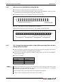
Each buffer memory address consists of 16 bits.
Fig. 3-14: Assignments of bits to a buffer memory address
NOTE
Do not write data in the "system areas" of the buffer memory. If data is written to any of the system
areas, the PLC system may not be operated properly. Some of the user areas contain partially system areas. Care must be taken when reading/writing to the buffer memory.
Also, do not write data (e.g. in a sequence program) to the buffer memory area where writing is
disabled. Doing so may cause malfunction.
Instructions for data exchange with the buffer memory
Communication between the PLC CPU and the buffer memory of special function modules is performed with FROM and TO instructions.
The buffer memory of a special function module can also accessed directly, e. g. with a MOV instruction. The special function module addressed in this way can be mounted on a base unit or an extension base unit but not in remote I/O stations.
Format of the device address: Un\Gn
– Un: Head address of the special function module
– Gn: Buffer memory address (decimal)
For example the device address U3\G11designates the buffer memory address 11 in the special function module with the head address 3 (X/Y30 to X/Y3F).
In this User´s Manual the latter form of addressing is used throughout.
For full documentation of all the instructions with examples please refer to the Programming Manual
for the A/Q series and the MELSEC System Q, art. no. 87431.
HART Analog Input Module ME1AD8HAI-Q
3 – 23
Detailed Description of the Module
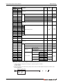
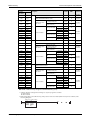
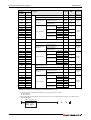
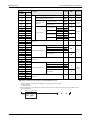
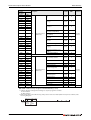
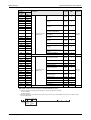
3.5.1
Buffer Memory
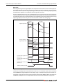
Buffer memory assignment
Address
Description
Hexadecimal
Decimal
0H
0
A/D conversion enable/disable setting
1H
1
CH1
2H
2
CH2
3H
3
CH3
4H
4
CH4
5H
5
CH5
6H
6
CH6
7H
7
CH7
8H
8
CH8
9H
9
System area
Average time/Average number of times/
Moving average/Time constant settings
AH
10
A/D conversion completed flag
BH
11
CH1 Digital output value
CH
12
CH2 Digital output value
DH
13
CH3 Digital output value
EH
14
CH4 Digital output value
FH
15
CH5 Digital output value
10H
16
CH6 Digital output value
11H
17
CH7 Digital output value
12H
18
CH8 Digital output value
13H
19
Error code
14H
20
Setting range (CH1 to CH4)
15H
21
Setting range (CH5 to CH8)
16H
22
17H
23
18H
24
Averaging process specification (CH1 to CH4)
19H
25
Averaging process specification (CH5 to CH8)
System area
Default
R/W*1
Reference
0000H
R/W*2
Section
3.5.2
0
R/W*2
Section
3.5.3
—
—
—
0
R
Section
3.5.4
0
R
Section
3.5.5
0
R
Section
3.5.6
0
R
Section
3.5.7
—
—
—
0
R/W*2
Section
3.5.8
Tab. 3-10: Buffer memory assignment of ME1AD8HAI-Q (1/16)
*1 Indicates whether reading from and writing to a sequence program are enabled.
R : Read enabled
W : Write enabled
*2 When writing data to the buffer memory, always use the interlock condition (buffer memory write condition) of the
following I/O signals.
Buffer memory writing condition
Y9
X9
Writing Operating Operating
request condition condition
setting
setting
request completed
flag
3 – 24
MOV
Buffer Memory
Detailed Description of the Module
Address
Hexadecimal
Decimal
1AH
26
to
to
1DH
29
1EH
30
1FH
31
20H
32
21H
33
22H
34
23H
35
24H
36
25H
37
26H
38
27H
39
28H
40
29H
41
2AH
42
2BH
43
2CH
44
2DH
45
2EH
46
Description
Default
R/W*1
Reference
System area
—
—
—
0
R
Section
3.5.9
—
—
—
CH1
CH2
CH3
CH4
CH5
CH6
CH7
CH8
Maximum value
Minimum value
Maximum value
Minimum value
Maximum value
Minimum value
Maximum value
Minimum value
Maximum value
Minimum value
Maximum value
Minimum value
Maximum value
Minimum value
Maximum value
Minimum value
System area
2FH
47
Input signal error detection setting
00FFH
R/W*2
Section
3.5.10
30H
48
Warning output setting
FFFFH
R/W*2
Section
3.5.11
31H
49
Input signal error detection flag
0
R
Section
3.5.12
32H
50
Warning output flag (Process alarm)
33H
51
Warning output flag (Rate alarm)
0
R
Section
3.5.13
34H
52
System area
—
—
—
00FFH
R/W*2
Section
3.5.14
0
R
Section
3.5.15
Lower limit value
0
Upper limit value
0
R/W*2
35H
53
Scaling enable/disable setting
CH1
36H
54
37H
55
CH2
38H
56
CH3
39H
57
CH4
3AH
58
CH5
3BH
59
CH6
3CH
60
CH7
3DH
61
CH8
3EH
62
3FH
63
40H
64
41H
65
42H
66
43H
67
Scaling value
CH1
Scaling
CH2
Scaling
CH3
Scaling
Lower limit value
0
Upper limit value
0
Lower limit value
0
Upper limit value
0
R/W*2
Section
3.5.16
R/W*2
Tab. 3-11: Buffer memory assignment of ME1AD8HAI-Q (2/16)
*1 Indicates whether reading from and writing to a sequence program are enabled.
R : Read enabled
W : Write enabled
*2 When writing data to the buffer memory, always use the interlock condition (buffer memory write condition) of the
following I/O signals.
Buffer memory writing condition
Y9
X9
Writing Operating Operating
request condition condition
setting
setting
request completed
flag
HART Analog Input Module ME1AD8HAI-Q
MOV
3 – 25
Detailed Description of the Module
Buffer Memory
Address
Hexadecimal
Decimal
44H
68
45H
69
46H
70
47H
71
48H
72
49H
73
4AH
74
4BH
75
4CH
76
4DH
77
4EH
78
to
to
55H
85
56H
86
57H
87
58H
88
Default
R/W*1
Lower limit value
0
Upper limit value
0
R/W*2
Description
CH4
Scaling
CH5
Scaling
CH6
Scaling
CH7
Scaling
CH8
Scaling
Lower limit value
0
Upper limit value
0
Lower limit value
0
Upper limit value
0
Lower limit value
0
Upper limit value
0
Lower limit value
0
Upper limit value
0
System area
—
Lower lower limit value
CH1
Process alarm
Lower upper limit value
0
Upper lower limit value
0
0
59H
89
Upper upper limit value
90
Lower lower limit value
0
5BH
91
Lower upper limit value
0
5CH
92
Upper lower limit value
0
5DH
93
Upper upper limit value
0
5EH
94
Lower lower limit value
0
5FH
95
Lower upper limit value
0
60H
96
Upper lower limit value
0
61H
97
Upper upper limit value
0
62H
98
Lower lower limit value
0
63H
99
Lower upper limit value
0
64H
100
Upper lower limit value
0
65H
101
Upper upper limit value
0
66H
102
Lower lower limit value
0
67H
103
Lower upper limit value
0
68H
104
Upper lower limit value
0
0
CH3
CH4
CH5
Process alarm
Process alarm
Process alarm
Process alarm
69H
105
Upper upper limit value
6AH
106
Lower lower limit value
0
6BH
107
Lower upper limit value
0
6CH
108
Upper lower limit value
0
6DH
109
Upper upper limit value
0
6EH
110
Lower lower limit value
0
6FH
111
Lower upper limit value
0
70H
112
Upper lower limit value
0
71H
113
Upper upper limit value
0
CH6
CH7
Process alarm
Process alarm
R/W*2
R/W*2
Section
3.5.16
R/W*2
R/W*2
—
—
R/W*2
Section
3.5.17
R/W*2
Section
3.5.17
R/W*2
Section
3.5.17
R/W*2
Section
3.5.17
R/W*2
Section
3.5.17
R/W*2
Section
3.5.17
R/W*2
Section
3.5.17
0
5AH
CH2
Reference
Tab. 3-12: Buffer memory assignment of ME1AD8HAI-Q (3/16)
*1 Indicates whether reading from and writing to a sequence program are enabled.
R : Read enabled
W : Write enabled
*2 When writing data to the buffer memory, always use the interlock condition (buffer memory write condition) of the
following I/O signals.
Buffer memory writing condition
Y9
X9
Writing Operating Operating
request condition condition
setting
setting
request completed
flag
3 – 26
MOV
Buffer Memory
Detailed Description of the Module
Address
Description
Default
Hexadecimal
Decimal
72H
114
Lower lower limit value
0
73H
115
Lower upper limit value
0
74H
116
Upper lower limit value
0
75H
117
Upper upper limit value
0
76H
118
77H
119
CH2
78H
120
CH3
CH8
79H
121
CH4
122
CH5
7BH
123
CH6
7CH
124
CH7
7DH
125
CH8
7EH
126
7FH
127
80H
128
129
82H
130
83H
131
84H
132
85H
133
86H
134
87H
135
88H
136
89H
137
8AH
138
8BH
139
Reference
R/W*2
Section
3.5.17
R/W*2
Section
3.5.18
CH1
7AH
81H
Process alarm
R/W*1
Rate alarm warning detection period
CH1
Rate alarm
CH2
Rate alarm
CH3
Rate alarm
CH4
Rate alarm
CH5
Rate alarm
CH6
Rate alarm
CH7
Rate alarm
CH8
Rate alarm
8CH
140
8DH
141
8EH
142
CH1
8FH
143
CH2
90H
144
CH3
91H
145
CH4
92H
146
CH5
93H
147
CH6
94H
148
CH7
95H
149
CH8
0
Upper limit value
0
Lower limit value
0
Upper limit value
0
Lower limit value
0
Upper limit value
0
Lower limit value
0
Upper limit value
0
Lower limit value
0
Upper limit value
0
Lower limit value
0
Upper limit value
0
Lower limit value
0
Upper limit value
0
Lower limit value
0
Upper limit value
0
Lower limit value
0
Input signal error detection setting value
50
R/W*2
R/W*2
R/W*2
R/W*2
R/W
*2
Section
3.5.19
R/W*2
R/W*2
R/W*2
R/W*2
Section
3.5.20
Tab. 3-13: Buffer memory assignment of ME1AD8HAI-Q (4/16)
*1 Indicates whether reading from and writing to a sequence program are enabled.
R : Read enabled
W : Write enabled
*2 When writing data to the buffer memory, always use the interlock condition (buffer memory write condition) of the
following I/O signals.
Buffer memory writing condition
Y9
X9
Writing Operating Operating
request condition condition
setting
setting
request completed
flag
HART Analog Input Module ME1AD8HAI-Q
MOV
3 – 27
Detailed Description of the Module
Buffer Memory
Address
Hexadecimal
Decimal
96H
150
to
to
9FH
159
A0H
160
A1H
161
Description
Default
R/W*1
Reference
System area
—
—
—
CH1 to CH8 enable
0000H
R/W*2
Section
3.5.21
Scan list
0000H
R
Section
3.5.22
HART
A2H
162
Current cycle time
0
R
A3H
163
Maximum cycle time
0
R
A4H
164
Minimum cycle time
0
R
A5H
165
—
—
—
3
R/W*2
Section
3.5.24
System area
—
—
—
HART device information refresh interval [seconds]
30
R/W*2
Section
3.5.25
System area
—
—
—
to
to
AFH
175
B0H
176
CH1
B1H
177
CH2
B2H
178
CH3
B3H
179
CH4
B4H
180
CH5
B5H
181
CH6
B6H
182
CH7
B7H
183
CH8
B8H
184
to
to
BEH
190
BFH
191
C0H
192
System area
HART maximum retries
Section
3.5.23
to
to
EFH
239
F0H
240
HART field device status
0000H
R
Section
3.5.26
F1H
241
HART extended field device status
0000H
R
Section
3.5.27
F2H
242
Primary value (PV),
secondary value (SV)
0000H
R
Tertiary value (TV),
fourth value (FV)
0000H
R
F3H
243
F4H
244
F5H
245
F6H
246
F7H
247
F8H
248
F9H
249
FAH
250
FBH
251
HART device variable status
CH1
Primary value (PV)
Secondary value
(SV)
Process variable
Tertiary value (TV)
Fourth value (FV)
Low word
0000H
High word
7FC0H
Low word
0000H
High word
7FC0H
Low word
0000H
High word
7FC0H
Low word
0000H
High word
7FC0H
Section
3.5.28
R
R
Section
3.5.29
R
R
Tab. 3-14: Buffer memory assignment of ME1AD8HAI-Q (5/16)
*1 Indicates whether reading from and writing to a sequence program are enabled.
R : Read enabled
W : Write enabled
*2 When writing data to the buffer memory, always use the interlock condition (buffer memory write condition) of the
following I/O signals.
Buffer memory writing condition
Y9
X9
Writing Operating Operating
request condition condition
setting
setting
request completed
flag
3 – 28
MOV
Buffer Memory
Detailed Description of the Module
Address
Hexadecimal
Decimal
FCH
252
FDH
253
FEH
254
FFH
255
Default
R/W*1
Reference
HART field device status
0000H
R
Section
3.5.26
HART extended field device status
0000H
R
Section
3.5.27
Primary value (PV),
secondary value (SV)
0000H
R
Tertiary value (TV),
fourth value (FV)
0000H
R
Description
HART device variable status
Section
3.5.28
100H
256
101H
257
102H
258
103H
259
104H
260
105H
261
106H
262
107H
263
108H
264
HART field device status
0000H
R
Section
3.5.26
109H
265
HART extended field device status
Sec 3.5.27
10AH
266
10BH
267
CH2
Primary value (PV)
Secondary value
(SV)
Process variable
Tertiary value (TV)
Fourth value (FV)
HART device variable status
Low word
0000H
High word
7FC0H
Low word
0000H
High word
7FC0H
Low word
0000H
High word
7FC0H
Low word
0000H
High word
7FC0H
R
R
Section
3.5.29
R
R
0000H
R
Primary value (PV),
secondary value (SV)
0000H
R
Tertiary value (TV),
fourth value (FV)
0000H
R
10CH
268
10DH
269
10EH
270
10FH
271
110H
272
111H
273
112H
274
113H
275
114H
276
HART field device status
0000H
R
Section
3.5.26
115H
277
HART extended field device status
Sec 3.5.27
116H
CH3
Secondary value
(SV)
Process variable
Tertiary value (TV)
Fourth value (FV)
278
117H
279
118H
280
119H
281
11AH
282
11BH
283
11CH
284
11DH
285
11EH
286
11FH
287
Primary value (PV)
HART device variable status
CH4
Low word
0000H
High word
7FC0H
Section
3.5.28
Low word
0000H
High word
7FC0H
Low word
0000H
High word
7FC0H
Low word
0000H
High word
7FC0H
R
R
Section
3.5.29
R
R
0000H
R
Primary value (PV),
secondary value (SV)
0000H
R
Tertiary value (TV),
fourth value (FV)
0000H
R
Primary value (PV)
Secondary value
(SV)
Process variable
Tertiary value (TV)
Fourth value (FV)
Low word
0000H
High word
7FC0H
Low word
0000H
High word
7FC0H
Low word
0000H
High word
7FC0H
Low word
0000H
High word
7FC0H
Section
3.5.28
R
R
Section
3.5.29
R
R
Tab. 3-15: Buffer memory assignment of ME1AD8HAI-Q (6/16)
*1 Indicates whether reading from and writing to a sequence program are enabled.
R : Read enabled
W : Write enabled
*2 When writing data to the buffer memory, always use the interlock condition (buffer memory write condition) of the
following I/O signals.
Buffer memory writing condition
Y9
X9
Writing Operating Operating
request condition condition
setting
setting
request completed
flag
HART Analog Input Module ME1AD8HAI-Q
MOV
3 – 29
Detailed Description of the Module
Buffer Memory
Address
Hexadecimal
Decimal
120H
288
121H
289
122H
290
123H
291
Default
R/W*1
Reference
HART field device status
0000H
R
Section
3.5.26
HART extended field device status
Sec 3.5.27
Description
HART device variable status
0000H
R
Primary value (PV),
secondary value (SV)
0000H
R
Tertiary value (TV),
fourth value (FV)
0000H
R
124H
292
125H
293
126H
294
127H
295
128H
296
129H
297
12AH
298
12BH
299
12CH
300
HART field device status
0000H
R
Section
3.5.26
12DH
301
HART extended field device status
0000H
R
Section
3.5.27
12EH
302
Primary value (PV),
secondary value (SV)
0000H
R
12FH
303
Tertiary value (TV),
fourth value (FV)
0000H
R
CH5
Primary value (PV)
Secondary value
(SV)
Process variable
Tertiary value (TV)
Fourth value (FV)
HART device variable status
Low word
0000H
High word
7FC0H
Section
3.5.28
Low word
0000H
High word
7FC0H
Low word
0000H
High word
7FC0H
Low word
0000H
High word
7FC0H
R
R
Section
3.5.28
304
305
132H
306
133H
307
134H
308
135H
309
136H
310
137H
311
138H
312
HART field device status
0000H
R
Section
3.5.26
139H
313
HART extended field device status
Sec 3.5.27
13AH
Secondary value
(SV)
Process variable
Tertiary value (TV)
Fourth value (FV)
314
13BH
315
13CH
316
13DH
317
13EH
318
13FH
319
140H
320
141H
321
142H
322
143H
323
HART device variable status
CH7
0000H
7FC0H
Section
3.5.29
130H
Primary value (PV)
High word
R
131H
CH6
Low word
R
Low word
0000H
High word
7FC0H
Low word
0000H
High word
7FC0H
Low word
0000H
High word
7FC0H
R
R
Section
3.5.29
R
R
0000H
R
Primary value (PV),
secondary value (SV)
0000H
R
Tertiary value (TV),
fourth value (FV)
0000H
R
Primary value (PV)
Secondary value
(SV)
Process variable
Tertiary value (TV)
Fourth value (FV)
Low word
0000H
High word
7FC0H
Low word
0000H
High word
7FC0H
Low word
0000H
High word
7FC0H
Low word
0000H
High word
7FC0H
Section
3.5.28
R
R
Section
3.5.29
R
R
Tab. 3-16: Buffer memory assignment of ME1AD8HAI-Q (7/16)
*1 Indicates whether reading from and writing to a sequence program are enabled.
R : Read enabled
W : Write enabled
*2 When writing data to the buffer memory, always use the interlock condition (buffer memory write condition) of the
following I/O signals.
Buffer memory writing condition
Y9
X9
Writing Operating Operating
request condition condition
setting
setting
request completed
flag
3 – 30
MOV
Buffer Memory
Detailed Description of the Module
Address
Hexadecimal
Decimal
144H
324
145H
325
146H
326
147H
327
148H
328
149H
329
14AH
330
14BH
331
14CH
332
14DH
333
14EH
334
14FH
335
150H
336
Default
R/W*1
Reference
HART field device status
0000H
R
Section
3.5.26
HART extended field device status
0000H
R
Section
3.5.27
Primary value (PV),
secondary value (SV)
0000H
R
Tertiary value (TV),
fourth value (FV)
0000H
R
Description
HART device variable status
CH8
Primary value (PV)
Secondary value
(SV)
Process variable
Tertiary value (TV)
Fourth value (FV)
Low word
0000H
High word
7FC0H
Low word
0000H
High word
7FC0H
Low word
0000H
High word
7FC0H
Low word
0000H
High word
7FC0H
—
to
to
15FH
351
System area
160H
352
Request flag
161H
353
Channel
0000H
162H
354
Code
0000H
163H
355
164H
356
to
to
1E3H
483
1E4H
484
HART Command (Request)
Answer flag
0000H
Channel
0000H
1F2H
498
Code
0000H
1F3H
499
1F4H
500
to
37FH
895
Section
3.5.30
—
497
628
—
R/W*2
—
496
to
—
R/W*2
1F1H
274H
R
0
1F0H
to
R
Data to be sent
to
627
Section
3.5.29
0
495
273H
R
Data size
1EFH
to
R
0
to
System area
HART Command (Answer)
Section
3.5.28
R
Section
3.5.31
Data size
0
Received data
0
R
—
—
System area
—
—
Tab. 3-17: Buffer memory assignment of ME1AD8HAI-Q (8/16)
*1 Indicates whether reading from and writing to a sequence program are enabled.
R : Read enabled
W : Write enabled
*2 When writing data to the buffer memory, always use the interlock condition (buffer memory write condition) of the
following I/O signals.
Buffer memory writing condition
Y9
X9
Writing Operating Operating
request condition condition
setting
setting
request completed
flag
HART Analog Input Module ME1AD8HAI-Q
MOV
3 – 31
Detailed Description of the Module
Buffer Memory
Address
Hexadecimal
Decimal
380H
896
to
to
383H
899
384H
900
to
to
393H
915
394H
916
to
to
39BH
923
39CH
924
39DH
925
39EH
926
39FH
927
3A0H
928
3A1H
929
3A2H
930
3A3H
931
Default
R/W*1
Tag
0000H
R
Message
0000H
R
Descriptor
0000H
R
Manufacturer ID / Expanded
manufacturer ID (HART 7)
0000H
R
Device Type / Expanded device
type (HART 7)
0000H
R
Device ID
0000H
R
Revisions
0000H
R
Device function flags
0000H
R
Long tag
0000H
R
Private label distributor code
(HART 7)
0000H
R
Device profile (HART 7)
0000H
R
—
—
Final assembly number
0000H
R
Date
0000H
R
Description
CH1
Information about
HART device
to
to
3B2H
946
3B3H
947
3B4H
948
3B5H
949
3B6H
950
3B7H
951
3B8H
952
3B9H
953
3BAH
954
Write Protect
0
R
3BBH
955
PV range unit code
0000H
R
3BCH
956
3BDH
957
PV Upper range value
0000H
R
PV Lower range value
0000H
R
PV Damping value
0000H
R
3BEH
958
System area
CH1
Information about
HART device
3BFH
959
3C0H
960
3C1H
961
3C2H
962
Transfer function
0000H
R
3C3H
963
PV Unit code
0000H
R
3C4H
964
SV Unit code
0000H
R
3C5H
965
TV Unit code
0000H
R
3C6H
966
FV Unit code
0000H
R
3C7H
967
—
—
System area
Reference
Section
3.5.32
—
Section
3.5.32
—
Tab. 3-18: Buffer memory assignment of ME1AD8HAI-Q (9/16)
*1 Indicates whether reading from and writing to a sequence program are enabled.
R : Read enabled
W : Write enabled
*2 When writing data to the buffer memory, always use the interlock condition (buffer memory write condition) of the
following I/O signals.
Buffer memory writing condition
Y9
X9
Writing Operating Operating
request condition condition
setting
setting
request completed
flag
3 – 32
MOV
Buffer Memory
Detailed Description of the Module
Address
Hexadecimal
Decimal
3C8H
968
to
to
3CBH
971
3CCH
972
to
to
3DBH
987
3DCH
988
to
to
3E3H
995
3E4H
996
3E5H
997
3E6H
998
3E7H
999
3E8H
1000
3E9H
1001
3EAH
1002
3EBH
1003
to
to
3FAH
1018
3FBH
1019
Default
R/W*1
Tag
0000H
R
Message
0000H
R
Descriptor
0000H
R
Manufacturer ID / Expanded
manufacturer ID (HART 7)
0000H
R
Device Type / Expanded device
type (HART 7)
0000H
R
Device ID
0000H
R
Revisions
0000H
R
Device function flags
0000H
R
Long tag
0000H
R
Private label distributor code
(HART 7)
0000H
R
Device profile (HART 7)
0000H
R
—
—
Final assembly number
0000H
R
Date
0000H
R
Description
CH2
Information about
HART device
3FCH
1020
3FDH
1021
3FEH
1022
3FFH
1023
400H
1024
401H
1025
402H
1026
Write Protect
0
R
403H
1027
PV range unit code
0000H
R
404H
1028
405H
1029
PV Upper range value
0000H
R
PV Lower range value
0000H
R
PV Damping value
0000H
R
406H
1030
System area
CH2
Information about
HART device
407H
1031
408H
1032
409H
1033
40AH
1034
Transfer function
0000H
R
40BH
1035
PV Unit code
0000H
R
40CH
1036
SV Unit code
0000H
R
40DH
1037
TV Unit code
0000H
R
40EH
1038
FV Unit code
0000H
R
40FH
1039
—
—
System area
Reference
Section
3.5.32
—
Section
3.5.32
—
Tab. 3-19: Buffer memory assignment of ME1AD8HAI-Q (10/16)
*1 Indicates whether reading from and writing to a sequence program are enabled.
R : Read enabled
W : Write enabled
*2 When writing data to the buffer memory, always use the interlock condition (buffer memory write condition) of the
following I/O signals.
Buffer memory writing condition
Y9
X9
Writing Operating Operating
request condition condition
setting
setting
request completed
flag
HART Analog Input Module ME1AD8HAI-Q
MOV
3 – 33
Detailed Description of the Module
Buffer Memory
Address
Hexadecimal
Decimal
410H
1040
to
to
413H
1043
414H
1044
to
to
423H
1059
424H
1060
to
to
42BH
1067
42CH
1068
42DH
1069
42EH
1070
42FH
1071
430H
1072
431H
1073
432H
1074
433H
1075
Default
R/W*1
Tag
0000H
R
Message
0000H
R
Descriptor
0000H
R
Manufacturer ID / Expanded
manufacturer ID (HART 7)
0000H
R
Device Type / Expanded device
type (HART 7)
0000H
R
Device ID
0000H
R
Revisions
0000H
R
Device function flags
0000H
R
Long tag
0000H
R
Private label distributor code
(HART 7)
0000H
R
Device profile (HART 7)
0000H
R
—
—
Final assembly number
0000H
R
Date
0000H
R
Description
CH3
Information about
HART device
to
to
442H
1090
443H
1091
444H
1092
445H
1093
446H
1094
447H
1095
448H
1096
449H
1097
44AH
1098
Write Protect
0
R
44BH
1099
PV range unit code
0000H
R
44CH
1100
44DH
1101
PV Upper range value
0000H
R
PV Lower range value
0000H
R
PV Damping value
0000H
R
44EH
1102
System area
CH3
Information about
HART device
44FH
1103
450H
1104
451H
1105
452H
1106
Transfer function
0000H
R
453H
1107
PV Unit code
0000H
R
454H
1108
SV Unit code
0000H
R
455H
1109
TV Unit code
0000H
R
456H
1110
FV Unit code
0000H
R
457H
1111
—
—
System area
Reference
Section
3.5.32
—
Section
3.5.32
—
Tab. 3-20: Buffer memory assignment of ME1AD8HAI-Q (11/16)
*1 Indicates whether reading from and writing to a sequence program are enabled.
R : Read enabled
W : Write enabled
*2 When writing data to the buffer memory, always use the interlock condition (buffer memory write condition) of the
following I/O signals.
Buffer memory writing condition
Y9
X9
Writing Operating Operating
request condition condition
setting
setting
request completed
flag
3 – 34
MOV
Buffer Memory
Detailed Description of the Module
Address
Hexadecimal
Decimal
458H
1112
to
to
45BH
1115
45CH
1116
to
to
46BH
1131
46CH
1132
to
to
473H
1139
474H
1140
475H
1141
476H
1142
477H
1143
478H
1144
479H
1145
47AH
1146
47BH
1147
to
to
48AH
1162
48BH
1163
Default
R/W*1
Tag
0000H
R
Message
0000H
R
Descriptor
0000H
R
Manufacturer ID / Expanded
manufacturer ID (HART 7)
0000H
R
Device Type / Expanded device
type (HART 7)
0000H
R
Device ID
0000H
R
Revisions
0000H
R
Device function flags
0000H
R
Long tag
0000H
R
Private label distributor code
(HART 7)
0000H
R
Device profile (HART 7)
0000H
R
—
—
Final assembly number
0000H
R
Date
0000H
R
Description
CH4
Information about
HART device
48CH
1164
48DH
1165
48EH
1166
48FH
1167
490H
1168
491H
1169
492H
1170
Write Protect
0
R
493H
1171
PV range unit code
0000H
R
494H
1172
495H
1173
PV Upper range value
0000H
R
PV Lower range value
0000H
R
PV Damping value
0000H
R
496H
1174
System area
CH4
Information about
HART device
497H
1175
498H
1176
499H
1177
49AH
1178
Transfer function
0000H
R
49BH
1179
PV Unit code
0000H
R
49CH
1180
SV Unit code
0000H
R
49DH
1181
TV Unit code
0000H
R
49EH
1182
FV Unit code
0000H
R
49FH
1183
—
—
System area
Reference
Section
3.5.32
—
Section
3.5.32
—
Tab. 3-21: Buffer memory assignment of ME1AD8HAI-Q (12/16)
*1 Indicates whether reading from and writing to a sequence program are enabled.
R : Read enabled
W : Write enabled
*2 When writing data to the buffer memory, always use the interlock condition (buffer memory write condition) of the
following I/O signals.
Buffer memory writing condition
Y9
X9
Writing Operating Operating
request condition condition
setting
setting
request completed
flag
HART Analog Input Module ME1AD8HAI-Q
MOV
3 – 35
Detailed Description of the Module
Buffer Memory
Address
Hexadecimal
Decimal
4A0H
1184
to
to
4A3H
1187
4A4H
1188
to
to
4B3H
1203
4B4H
1204
to
to
4BBH
1211
4BCH
1212
4BDH
1213
4BEH
1214
4BFH
1215
4C0H
1216
4C1H
1217
4C2
1218
4C3H
1219
Default
R/W*1
Tag
0000H
R
Message
0000H
R
Descriptor
0000H
R
Manufacturer ID / Expanded
manufacturer ID (HART 7)
0000H
R
Device Type / Expanded device
type (HART 7)
0000H
R
Device ID
0000H
R
Revisions
0000H
R
Device function flags
0000H
R
Long tag
0000H
R
Private label distributor code
(HART 7)
0000H
R
Device profile (HART 7)
0000H
R
—
—
Final assembly number
0000H
R
Date
0000H
R
Description
CH5
Information about
HART device
to
to
4D2H
1234
4D3H
1235
4D4H
1236
4D5H
1237
4D6H
1238
4D7H
1239
4D8H
1240
4D9H
1241
4DAH
1242
Write Protect
0
R
4DBH
1243
PV range unit code
0000H
R
4DCH
1244
4DDH
1245
PV Upper range value
0000H
R
PV Lower range value
0000H
R
PV Damping value
0000H
R
System area
CH5
Information about
HART device
4DEH
1246
4DFH
1247
4E0H
1248
4E1H
1249
4E2H
1250
Transfer function
0000H
R
4E3H
1251
PV Unit code
0000H
R
4E4H
1252
SV Unit code
0000H
R
4E5H
1253
TV Unit code
0000H
R
4E6H
1254
FV Unit code
0000H
R
4E7H
1255
—
—
System area
Reference
Section
3.5.32
—
Section
3.5.32
—
Tab. 3-22: Buffer memory assignment of ME1AD8HAI-Q (13/16)
*1 Indicates whether reading from and writing to a sequence program are enabled.
R : Read enabled
W : Write enabled
*2 When writing data to the buffer memory, always use the interlock condition (buffer memory write condition) of the
following I/O signals.
Buffer memory writing condition
Y9
X9
Writing Operating Operating
request condition condition
setting
setting
request completed
flag
3 – 36
MOV
Buffer Memory
Detailed Description of the Module
Address
Hexadecimal
Decimal
4E8H
1256
to
to
4EBH
1259
4ECH
1260
to
to
4FBH
1275
4FCH
1276
to
to
503H
1283
504H
1284
505H
1285
506H
1286
507H
1287
508H
1288
509H
1289
50AH
1290
50BH
1291
to
to
51AH
1306
51BH
1307
Default
R/W*1
Tag
0000H
R
Message
0000H
R
Descriptor
0000H
R
Manufacturer ID / Expanded
manufacturer ID (HART 7)
0000H
R
Device Type / Expanded device
type (HART 7)
0000H
R
Device ID
0000H
R
Revisions
0000H
R
Device function flags
0000H
R
Long tag
0000H
R
Private label distributor code
(HART 7)
0000H
R
Device profile (HART 7)
0000H
R
—
—
Final assembly number
0000H
R
Date
0000H
R
Description
CH6
Information about
HART device
51CH
1308
51DH
1309
51EH
1310
51FH
1311
520H
1312
521H
1313
522H
1314
Write Protect
0
R
523H
1315
PV range unit code
0000H
R
524H
1316
525H
1317
PV Upper range value
0000H
R
PV Lower range value
0000H
R
PV Damping value
0000H
R
526H
1318
System area
CH6
Information about
HART device
527H
1319
528H
1320
529H
1321
52AH
1322
Transfer function
0000H
R
52BH
1323
PV Unit code
0000H
R
52CH
1324
SV Unit code
0000H
R
52DH
1325
TV Unit code
0000H
R
52EH
1326
FV Unit code
0000H
R
52FH
1327
—
—
System area
Reference
Section
3.5.32
—
Section
3.5.32
—
Tab. 3-23: Buffer memory assignment of ME1AD8HAI-Q (14/16)
*1 Indicates whether reading from and writing to a sequence program are enabled.
R : Read enabled
W : Write enabled
*2 When writing data to the buffer memory, always use the interlock condition (buffer memory write condition) of the
following I/O signals.
Buffer memory writing condition
Y9
X9
Writing Operating Operating
request condition condition
setting
setting
request completed
flag
HART Analog Input Module ME1AD8HAI-Q
MOV
3 – 37
Detailed Description of the Module
Buffer Memory
Address
Hexadecimal
Decimal
530H
1328
to
to
533H
1331
534H
1332
to
to
543H
1347
544H
1348
to
to
54BH
1355
54CH
1356
54DH
1357
54EH
1358
54FH
1359
550H
1360
551H
1361
552H
1362
553H
1363
Default
R/W*1
Tag
0000H
R
Message
0000H
R
Descriptor
0000H
R
Manufacturer ID / Expanded
manufacturer ID (HART 7)
0000H
R
Device Type / Expanded device
type (HART 7)
0000H
R
Device ID
0000H
R
Revisions
0000H
R
Device function flags
0000H
R
Long tag
0000H
R
Private label distributor code
(HART 7)
0000H
R
Device profile (HART 7)
0000H
R
—
—
Final assembly number
0000H
R
Date
0000H
R
Description
CH7
Information about
HART device
to
to
562H
1378
563H
1379
564H
1380
565H
1381
566H
1382
567H
1383
568H
1384
569H
1385
56AH
1386
Write Protect
0
R
56BH
1387
PV range unit code
0000H
R
56CH
1388
56DH
1389
PV Upper range value
0000H
R
PV Lower range value
0000H
R
PV Damping value
0000H
R
56EH
1390
System area
CH7
Information about
HART device
56FH
1391
570H
1392
571H
1393
572H
1394
Transfer function
0000H
R
573H
1395
PV Unit code
0000H
R
574H
1396
SV Unit code
0000H
R
575H
1397
TV Unit code
0000H
R
576H
1398
FV Unit code
0000H
R
577H
1399
—
—
System area
Reference
Section
3.5.32
—
Section
3.5.32
—
Tab. 3-24: Buffer memory assignment of ME1AD8HAI-Q (15/16)
*1 Indicates whether reading from and writing to a sequence program are enabled.
R : Read enabled
W : Write enabled
*2 When writing data to the buffer memory, always use the interlock condition (buffer memory write condition) of the
following I/O signals.
Buffer memory writing condition
Y9
X9
Writing Operating Operating
request condition condition
setting
setting
request completed
flag
3 – 38
MOV
Buffer Memory
Detailed Description of the Module
Address
Hexadecimal
Decimal
578H
1400
to
to
57BH
1403
57CH
1404
to
to
58BH
1419
58CH
1420
to
to
593H
1427
594H
1428
595H
1429
596H
1430
597H
1431
598H
1432
599H
1433
59AH
1434
59BH
1435
to
to
5AAH
1450
5ABH
1451
Default
R/W*1
Tag
0000H
R
Message
0000H
R
Descriptor
0000H
R
Manufacturer ID / Expanded
manufacturer ID (HART 7)
0000H
R
Device Type / Expanded device
type (HART 7)
0000H
R
Device ID
0000H
R
Revisions
0000H
R
Device function flags
0000H
R
Long tag
0000H
R
Private label distributor code
(HART 7)
0000H
R
Device profile (HART 7)
0000H
R
—
—
Final assembly number
0000H
R
Date
0000H
R
Description
CH8
Information about
HART device
5ACH
1452
5ADH
1453
5AEH
1454
5AFH
1455
5B0H
1456
5B1H
1457
5B2H
1458
Write Protect
0
R
5B3H
1459
PV range unit code
0000H
R
5B4H
1460
5B5H
1461
PV Upper range value
0000H
R
PV Lower range value
0000H
R
PV Damping value
0000H
R
5B6H
1462
System area
CH8
Information about
HART device
5B7H
1463
5B8H
1464
5B9H
1465
5BAH
1466
Transfer function
0000H
R
5BBH
1467
PV Unit code
0000H
R
5BCH
1468
SV Unit code
0000H
R
5BDH
1469
TV Unit code
0000H
R
5BEH
1470
FV Unit code
0000H
R
5BFH
1471
—
—
System area
Reference
Section
3.5.32
—
Section
3.5.32
—
Tab. 3-25: Buffer memory assignment of ME1AD8HAI-Q (16/16)
*1 Indicates whether reading from and writing to a sequence program are enabled.
R : Read enabled
W : Write enabled
*2 When writing data to the buffer memory, always use the interlock condition (buffer memory write condition) of the
following I/O signals.
Buffer memory writing condition
Y9
X9
Writing Operating Operating
request condition condition
setting
setting
request completed
flag
HART Analog Input Module ME1AD8HAI-Q
MOV
3 – 39
Detailed Description of the Module
3.5.2
Buffer Memory
A/D conversion enable/disable setting (Un\G0)
● Set whether to enable or disable A/D conversion for each channel.
● It is necessary to set the operating condition setting request (Y9) to ON/OFF in order to validate
the A/D conversion enable/disable setting. (Refer to section 3.4.2)
● The ME1AD8HAI-Q is preset to enable A/D conversion on all channels.
b15 b14 b13 b12 b11
Un\G0
0
0
0
0
0
b10
b9
b8
0
0
0
b7
b6
b5
b4
b3
b2
b1
b0
CH8 CH7 CH6 CH5 CH4 CH3 CH2 CH1
0: A/D conversion enable
1: A/D conversion disable
Information of b8 to b15 is fixed to 0.
Fig. 3-15: Assignment of the bits in buffer memory address 0
Example: When channels for A/D conversion are 1 and 3, 00FAH is stored into Un\G0.
b15 b14 b13 b12 b11
0
0
0
0
0
b10
b9
b8
b7
b6
b5
b4
b3
b2
b1
b0
0
0
0
1
1
1
1
1
0
1
0
00FAH
CH8 CH7 CH6 CH5 CH4 CH3 CH2 CH1
0
0
F
A
Fig. 3-16: In this example A/D conversion for the channels 1 and 3 is enabled.
3.5.3
CH Average time/Average number of times/Moving average/Time constant
settings (Un\G1 to Un\G8)
● Set the average time, average count, moving average count or primary delay filter time constant
for each channel for which averaging processing is specified.
● To validate the setting, the operating condition setting request (Y9) must be turned ON/OFF.
(Refer to section 3.4.2)
● 0 is set as the default.
Processing method
Setting value
Time averaging
320 to 5000 (ms)
Count averaging
4 to 500 (times)
Moving average
2 to 60 (times)
Primary delay filter
80 to 5000 (ms)
Tab. 3-26: Setting ranges for processing
NOTES
Writing a value outside the range to a channel will cause an error, storing an error code in Error
code (Un\G19) and turning ON the Error flag (XF). If this occurs, A/D conversion is performed
based on the setting before the error detection.
Since the default setting is 0, change it for the selected processing method.
If a value is set to a sampling-processing channel, the value is ignored.
3 – 40
Buffer Memory
3.5.4
Detailed Description of the Module
A/D conversion completed flag (Un\G10)
● When A/D conversion of a conversion-enabled channel is complete, the A/D conversion completed flag is set to 1.
The A/D conversion completed flag (XE) turns ON when conversion for all A/D-conversionenabled channels is complete.
● When the operating condition setting request (Y9) is set to ON, the flag returns to the default
setting of 0, and changes to 1 when A/D conversion is complete.
b15 b14 b13 b12 b11
Un\G10
0
0
0
0
0
b10
b9
b8
0
0
0
b7
b6
b5
b4
b3
b2
b1
b0
CH8 CH7 CH6 CH5 CH4 CH3 CH2 CH1
1 : A/D conversion completed
0 : A/D conversion in progress or not used
Information of b8 to b15 is fixed to 0.
Fig. 3-17: Assignment of the bits in buffer memory address 10
● Example
When all A/D conversions of conversion-enabled channels 1 and 2 are completed, 0003H is stored
into the buffer memory address 10 (Un\G10).
b15 b14 b13 b12 b11
0
0
0
0
0
b10
b9
b8
b7
b6
b5
b4
b3
b2
b1
b0
0
0
0
0
0
0
0
0
0
1
1
0003H
CH8 CH7 CH6 CH5 CH4 CH3 CH2 CH1
0
0
3
0
Fig. 3-18: A/D conversion of channels 1 and 2 is completed
3.5.5
CH digital output value (Un\G11 to Un\G18)
Digital values converted from analog values are stored for respective channels.
b15 b14 b13b12 b11 b10 b9 b8 b7 b6 b5 b4 b3 b2 b1 b0
Un\G11 to Un\G18
Bit data section
Sign bit
1: Negative
0: Positive
Fig. 3-19: Digital values are stored in 16-bit signed binary format
HART Analog Input Module ME1AD8HAI-Q
3 – 41
Detailed Description of the Module
3.5.6
Buffer Memory
Write data error code (Un\G19)
An error code generated by the HART analog input module is stored here. Refer to section 6.1 for
details of the error codes.
3.5.7
Setting range (Un\G20, Un\G21)
These areas are used to confirm the input ranges of respective channels. A value set in the input range
setting is stored in the corresponding channel area as shown below.
b15
to
b12 b11
to
b8 b7
to
b4 b3
to
Un\G20
CH4
CH3
CH2
CH1
Un\G21
CH8
CH7
CH6
CH5
b0
Fig. 3-20: Each buffer memory address stores the input setting range for four channels
The correlation between the input range and the settings in Un\G20 and Un\G21 is shown in the following table.
Input range
Setting value
4 to 20 (mA)
0H
0 to 20 (mA)
1H
Illegal (not allowed)
Other settings
Tab. 3-27: Input ranges of the ME1AD8HAI-Q
3 – 42
Buffer Memory
3.5.8
Detailed Description of the Module
Averaging process specification (Un\G24, Un\G25)
● Specify whether to perform sampling processing or averaging processing (time averaging, count
averaging, moving average, or primary delay filter) for each channel.
● To validate the setting, the operating condition setting request (Y9) must be turned ON/OFF.
(Refer to section 3.4.2)
● By default, sampling processing(0H) is set for all channels.
b15
to
b12 b11
to
b8 b7
to
b4 b3
to
b0
Un\G24
CH4
CH3
CH2
CH1
Un\G25
CH8
CH7
CH6
CH5
Fig. 3-21: Each buffer memory address stores the averaging process specification for four
channels
The table below shows the correlation between the settings in Un\G24 and Un\G25 and the processing method.
Processing method
Setting value
Sampling processing
0H (Default)
Time averaging
1H
Count averaging
2H
Moving average
3H
Primary delay filter
4H
Tab. 3-28: Processing methods for the ME1AD8HAI-Q
● Example
When setting channel 1 to count averaging, channel 2 to time averaging, channel 3 to primary
delay filter, and channel 4 to sampling processing, store 412H into Un\G24.
b15 b14 b13 b12 b11
0
0
0
0
CH4
0
0
b10
b9
b8
b7
b6
b5
b4
b3
b2
b1
b0
1
0
0
0
0
0
1
0
0
1
0
CH3
4
CH2
CH1
1
2
412H
Fig. 3-22: Setting example for the channels 1 to 4 (Un\G24)
NOTE
When a value outside the above setting range has been written to a channel, sampling processing
is applied to the channel.
HART Analog Input Module ME1AD8HAI-Q
3 – 43
Detailed Description of the Module
3.5.9
Buffer Memory
CH maximum value/minimum value storage area (Un\G30 to Un\G45)
● The maximum value and minimum value of converted digital values are stored in 16-bit signed
binary format for each channel.
● The stored values for all channels will be cleared to 0 when the operating condition setting request
(Y9) is set to ON and the setting is changed or when the maximum value/minimum value reset
request (YD) is set to ON.
● The maximum and minimum values are stored at intervals of the sample processing time, even
if averaging processing is specified for the channel.
● When the scaling function is enabled, maximum/minimum values after scaling conversion are
stored.
3.5.10
Input signal error detection setting (Un\G47)
● This area is used to set whether the input signal error detection will be enabled or disabled for
each channel.
● To validate the input signal error detection setting, the operating condition setting request (Y9)
must be turned ON/OFF. (Refer to section 3.4.2)
● All channels are set to disable as the default setting.
b15 b14 b13 b12 b11
Un\G47
0
0
0
0
b10
b9
b8
0
0
0
0
b7
b6
b5
b4
b3
b2
b1
b0
CH8 CH7 CH6 CH5 CH4 CH3 CH2 CH1
0: Enable
1: Disable
Information of b8 to b15 is fixed to 0.
Fig. 3-23: Assignment of the bits in buffer memory address 47
● Example
To enable input signal error detection for channels 1 and 3, store 00FAH into Un\G47.
b15 b14 b13 b12 b11
0
0
0
0
0
b10
b9
b8
b7
b6
b5
b4
b3
b2
b1
b0
0
0
0
1
1
1
1
1
0
1
0
CH8 CH7 CH6 CH1 CH4 CH3 CH2 CH1
0
0
F
Fig. 3-24: Input signal error detection for channels 1 and 3 is enabled
3 – 44
A
00FAH
Buffer Memory
3.5.11
Detailed Description of the Module
Warning output settings (Un\G48)
● This area is used to set whether the process alarm/rate alarm warning is to be output or stopped
on a channel basis.
● To validate the warning output setting, the operating condition setting request (Y9) must be
turned ON/OFF. (Refer to section 3.4.2)
● By default, all channels are set to disable.
b15 b14 b13 b12 b11
b10
b9
b8
b7
b6
b5
b4
b3
b2
b1
b0
Un\G48 CH8 CH7 CH6 CH5 CH4 CH3 CH2 CH1 CH8 CH7 CH6 CH5 CH4 CH3 CH2 CH1
Rate alarm setting
Process alarm setting
0: Enable, 1: Disable
Fig. 3-25: Assignment of the bits in buffer memory address 48
● Example
When process alarm warning output is enabled for channel 7 and rate alarm warning output is
enabled for channel 3, FBBFH is stored into Un\G48.
b15 b14 b13 b12 b11
1
1
1
1
1
b10
b9
b8
b7
b6
b5
b4
b3
b2
b1
b0
0
1
1
1
0
1
1
1
1
1
1
FBBFH
CH8 CH7 CH6 CH5 CH4 CH3 CH2 CH1 CH8 CH7 CH6 CH5 CH4 CH3 CH2 CH1
F
B
B
F
Fig. 3-26: Rate alarm warning output is enabled for channel 3
Process alarm warning output is enabled for channel 7
HART Analog Input Module ME1AD8HAI-Q
3 – 45
Detailed Description of the Module
3.5.12
Buffer Memory
Input signal error detection flag (Un\G49)
● If the analog input value detected falls outside the setting range set to the CH input signal error
detection setting value (Un\G142 to Un\G149), the Input signal error detection flag for the
corresponding channel turns to 1.
● By bringing the analog input value within the setting range and turning ON the Error clear request
(YF), the Input signal error detection flag turns OFF.
● If an error is detected on any one of the channels for which input signal error detection is enabled,
the Input signal error detection signal (XC) also turns ON.
● When the operating condition setting request (Y9) is turned ON, the Input signal error detection
flag is cleared.
b15 b14 b13 b12 b11
Un\G49
0
0
0
0
0
b10
b9
b8
0
0
0
b7
b6
b5
b3
b2
b1
b0
CH8 CH7 CH6 CH5 CH4 CH3 CH2 CH1
Information of b8 to b15 is fixed to 0.
Fig. 3-27: Assignment of the bits in buffer memory address 49
3 – 46
b4
0: Normal
1: Input signal error
Buffer Memory
3.5.13
Detailed Description of the Module
Warning output flag (Un\G50, Un\G51)
● If the digital output value or its varying rate falls outside the setting range set in the following
buffer memory addresses, the warning output flag for the corresponding channel turns to 1:
– CH process alarm upper/lower limit value (Un\G86 to Un\G117)
– CH rate alarm upper/lower limit value (Un\G126 to Un\G141)
● For both the process alarm and rate alarm, whether the warning is for the upper or lower limit
value can be checked on a channel basis.
● When the digital output value or its varying rate returns to within the setting range, the warning
output flag is automatically reset.
● If a warning is detected on any one of the channels for which A/D conversion and process alarm
or rate alarm warning output are enabled, the Warning output signal (X8) also turns ON.
● When the operating condition setting request (Y9) is turned ON, the warning output flag is cleared.
b15 b14 b13 b12 b11
Un\G50
(Process alarm)
b10
b9
b8
b7
b6
b5
b4
b3
b2
b1
b0
CH8 CH8 CH7 CH7 CH6 CH6 CH5 CH5 CH4 CH4 CH3 CH3 CH2 CH2 CH1 CH1
Lower Upper Lower Upper Lower
limit
limit
limit
limit
limit
value value value value value
Upper Lower Upper Lower Upper Lower Upper Lower Upper Lower Upper
limit
limit
limit
limit
limit
limit
limit
limit
limit
limit
limit
value value value value value value value value value value value
0: Normal,
1: Alarm ON
b15 b14 b13 b12 b11
b10
b9
b8
b7
b6
b5
b4
b3
b2
b1
b0
CH8 CH8 CH7 CH7 CH6 CH6 CH5 CH5 CH4 CH4 CH3 CH3 CH2 CH2 CH1 CH1
Un\G51
(Rate alarm)
Lower Upper Lower Upper Lower
limit
limit
limit
limit
limit
value value value value value
Upper Lower Upper Lower Upper Lower Upper Lower Upper Lower Upper
limit
limit
limit
limit
limit
limit
limit
limit
limit
limit
limit
value value value value value value value value value value value
0: Normal,
1: Alarm ON
Fig. 3-28: For each channel two bits for upper and lower limit alarms are provided
3.5.14
Scaling enable/disable setting (Un\G53)
● Whether to enable or disable the scaling function for each channel is set in this area.
● To validate the scaling function, the operating condition setting request (Y9) must be turned ON/OFF.
(Refer to section 3.4.2)
● All channels are defaulted to "Disable".
b15 b14 b13 b12 b11
Un\G53
0
0
0
0
0
b10
b9
b8
0
0
0
b7
b6
b5
b4
b3
b2
b1
b0
CH8 CH7 CH6 CH5 CH4 CH3 CH2 CH1
Information of b8 to b15 is fixed to 0.
0: Enable the scaling function for the correspondent channel
1: Disable the scaling function for the correspondent channel
Fig. 3-29: Assignment of the bits in buffer memory address 53
NOTE
When the Scaling enable/disable setting (Un\G53) is set to "Disable", 0s are stored in the CH
scaling value storage area (Un\G54 to Un\G61).
HART Analog Input Module ME1AD8HAI-Q
3 – 47
Detailed Description of the Module
3.5.15
Buffer Memory
CH scaling value storage area (Un\G54 to Un\G61)
● Digital output values after scaling conversion are stored for respective channels.
● Scaling conversion values are stored as 16-bit signed binaries.
b15 b14 b13b12 b11 b10 b9 b8 b7 b6 b5 b4 b3 b2 b1 b0
Un\G54 to Un\G61
Bit data section
Sign bit
1: Negative
0: Positive
Fig. 3-30: Format of the scaling values
3.5.16
CH scaling upper/lower limit value (Un\G62 to Un\G77)
● Set a scaling conversion range for each channel.
● To validate the setting, the operating condition setting request (Y9) must be turned ON/OFF. (Refer
to section 3.4.2)
● The setting range is -32000 to 32000.
Refer to section 3.3.5 for details of the scaling function.
NOTES
Setting a value outside the above setting range or a value that does not meet the inequality "Upper
limit > Lower limit" will cause an error. If this occurs, an error code is stored in Error code (Un\G19) followed by ON of the Error flag (XF), and the module will operate under the setting before the error.
Since the default setting is 0, changing of the setting is required for operation.
When the Scaling enable/disable setting (Un\G53) is set to "Disable", scaling upper/lower limit values
are ignored.
3.5.17
CH process alarm upper/lower limit value (Un\G86 to Un\G117)
● Set the range of the digital output value on a channel basis.
● To validate the setting, the operating condition setting request (Y9) must be turned ON/OFF.
(Refer to section 3.4.2)
● The setting range is -32768 to 32767.
● Make four kinds of settings for process alarms:
– upper upper limit value
– upper lower limit value
– lower upper limit value
– lower lower limit value.
● Refer to section 3.3.4 for details of the process alarm.
3 – 48
Buffer Memory
NOTES
Detailed Description of the Module
If a value outside the above setting range is set or if a value that does not satisfy the condition of
“lower lower limit value 울 lower upper limit value 울 upper lower limit value 울 upper upper limit
value” is set, it results in an error. An error code is stored into the Error code (Un\G19), the Error flag
(XF) turns ON, and operation is performed based on the setting before the error detection.
Since the default setting is 0, changing of the setting is required for operation.
When "Enable" is set in the Scaling enable/disable setting (Un\G53), always take into account the
scaling conversion before setting values.
3.5.18
CH rate alarm warning detection period (Un\G118 to Un\G125)
● Set a period, with which the varying rate of the digital output value will be checked, on a channel
basis.
● To validate the setting, the operating condition setting request (Y9) must be turned ON/OFF.
(Refer to section 3.4.2)
● The setting range is 80 to 5000 ms.
The value must be a multiple of the cycle time (80 ms)
● When time averaging or count averaging has been specified for averaging process specification,
set the rate alarm warning detection period as a multiple of the time averaging or count averaging
conversion period.
NOTE
If the count value set for the count averaging is 10, the conversion cycle for count averaging is:
10 (times) x 80 (ms) = 800 (ms)
Therefore, set a multiple of 800, such as 1600 or 3200, to the rate alarm warning detection period.
● The default setting is 0 ms.
● Refer to section 3.3.4 for details of the rate alarm.
NOTES
If a value outside the above setting range is written to a channel, an error occurs, and an error code is
stored into the Error code (Un\G19). The Error flag (XF) turns ON, and the time or count averaging or
rate alarm processing is performed based on the setting before the error detection.
Since the default setting is 0, changing of the setting is required for operation.
If the upper limit value and lower limit value settings of the rate alarm are small, the warning output
may turn ON due to overreaction to disturbance or like. This overreaction can be avoided by increasing the setting of the rate alarm warning detection period.
HART Analog Input Module ME1AD8HAI-Q
3 – 49
Detailed Description of the Module
3.5.19
Buffer Memory
CH rate alarm upper/lower limit value (Un\G126 to Un\G141)
● Set the varying rate range of the digital output value on a channel basis.
● To validate the setting, the operating condition setting request (Y9) must be turned ON/OFF.
(Refer to section 3.4.2)
● The setting range is -32768 to 32767 (-3276.8 to 3276.7 %). Set the value in 0.1 %/s increments.
Example: When setting the rate alarm upper limit value to 30 % per second, store 300 into the
buffer memory.
● Refer to section 3.3.4 for details of the rate alarm.
3.5.20
CH input signal error detection setting value (Un\G142 to Un\G149)
● Set the value, by which an error of the input analog value will be detected, on a channel basis.
● To validate the setting, the Operating condition setting request (Y9) must be turned ON/OFF.
(Refer to section 3.4.2)
● The setting range is 0 to 250 (0 to 25.0 %). Set the value in 0.1 % increments.
Example: When setting the input signal error detection setting value to 15 %, store 150 into the
buffer memory.
● Based on this input signal error detection setting value, the input signal upper and lower limit
values are calculated as shown below. The calculated values vary depending on the input range.
– Input signal error detection upper limit value
= gain value of corresponding range + (gain value of corresponding range - offset value of
corresponding range) x (input signal error detection setting value /1000)
– Input signal error detection lower limit value
= offset value of corresponding range – (gain value of corresponding range - offset value of
corresponding range) x (input signal error detection setting value /1000)
NOTES
Set the input signal error detection upper limit value to less than 25 mA.
If the setting is 25 mA or more, the error may not be detected.
If a value outside the setting range is set, an error occurs and an error code is stored in the Error
code (Un\G19). In this case, the operation is performed based on the setting before the error
detection.
3 – 50
Buffer Memory
3.5.21
Detailed Description of the Module
HART enable (Un\G160)
● After the bit corresponded to each channel is set, HART communication will be automatically
started in the indicated channel.
● This setting is independent from the "A/D Conversion Enable/Disable" setting and the "Setting
Range" setting. (The HART communication can be enabled or disabled even if the A/D conversion
is disabled or the setting range is 0 to 20 mA.)
b15 b14 b13 b12 b11
Un\G160
0
0
0
0
0
b10
b9
b8
0
0
0
b7
b6
b5
b4
b3
b2
b1
b0
CH8 CH7 CH6 CH5 CH4 CH3 CH2 CH1
Information of b8 to b15 is fixed to 0.
1: HART enabled
0: HART disabled (default)
Fig. 3-31: Assignment of the bits in buffer memory address 160
3.5.22
HART scan list (Un\G161)
● After HART functionality is enabled, the ME1AD8HAI-Q will automatically detect the HART device
which is connected with the enabled channel. After the device information are stored into the
buffer memory, the corresponding bit in the "HART Scan list" is set. (Refer to the figures below.)
b15 b14 b13 b12 b11
Un\G161
0
0
0
0
0
b10
b9
b8
0
0
0
b7
b6
b5
b4
b3
b2
b1
b0
CH8 CH7 CH6 CH5 CH4 CH3 CH2 CH1
1: HART device found
0: HART device not found
Information of b8 to b15 is fixed to 0.
Fig. 3-32: Assignment of the bits in the HART scan list (buffer memory address 161)
ON
Bit of "HART enable"
(Un\G160)
�
�
Normal HART
communication
Looking for
HART device
Device Information
for each channel
(Un\G896 to
Un\G1470)
0
Device information
Looking for
HART device
Keep Device
Information
ON
Bit of "HART scan list"
(Un\G161)
Fig. 3-33: Operation when HART device is detected and missing
쐃 When a HART device is detected, the device information is stored, the HART communication is
initialized, and the corresponding bit in the HART scan list is set.
쐇 When the HART communication is interrupted due to a missing HART device, the corresponding
bit in the HART scan list is reset and the HART device information is kept.
HART Analog Input Module ME1AD8HAI-Q
3 – 51
Detailed Description of the Module
Buffer Memory
�
ON
Bit of "HART enable"
(Un\G160)
�
Normal HART
communication
Looking for
HART device
Device Information
for each channel
(Un\G896 to
Un\G1470)
0
�
Looking for
HART device
Device information
0
ON
Bit of "HART scan list"
(Un\G161)
Fig. 3-34: Operation when HART functionality is disabled
쐃 When a HART device is detected, the device information is stored, the HART communication is
initialized, and the corresponding bit in the HART scan list is set.
쐇 When the HART communication is disabled, the corresponding bit in the HART scan list is reset
and the HART device information is cleared.
쐋 Since the HART enable bit in Un\G160 is reset, the HART communication is stopped.
3.5.23
HART Cycle Time (Un\G162 to Un\G164)
● The current, maximum and minimum HART cycle time is stored in Un\G162, Un\G163 and
Un\G164 respectively.
● The HART cycle time is the total time required for accessing each HART enabled channel or rather
the time period between two accesses to the same HART channel.
● The unit of the HART cycle time is 10 ms.
● These values are reset after a power reset or PLC CPU reset.
3.5.24
HART Maximum Retries (Un\G176 to Un\G183)
● Set the maximum number of command retries for each HART channel.
● The range is 0 to 30, default is 3 retries.
3.5.25
HART device information refresh interval (Un\G191)
● Set the maximum interval in which the device information shall be read from a HART device.
● The range is 0 to 60 seconds, default is 30 seconds.
● This setting can speed up the FDT/DTM communication when changing configuration data via
the DTM. The affected HART device information data is located in the buffer memory addresses
Un\G896 to Un\G1470. The HART Process Variables (Un\G240 to Un\G335) are not affected, they
are updated cyclically.
3 – 52
Buffer Memory
3.5.26
Detailed Description of the Module
HART Field Device Status (Un\G240, Un\G252, Un\G264...)
Information about the status of the HART field device are stored in the corresponding buffer memory
address (Channel 1: Un\G240, ch. 2: Un\252, ch3: Un\G264 etc.).
Un\G240
Un\G252
Un\G264
Un\G276
Un\G288
Un\G300
Un\G312
Un\G324
b15 b14 b13 b12 b11
0
b10
b9
HART
field
0
0 device
0 error
0 codes
0
b8
0
b7
b6
b5
b4
b3
b2
b1
b0
HART field device status
Communication error
1: Bits b8 to b14 are set according to a communication error
0: Command specific response code is stored in b8 to b14
Fig. 3-35: Assignment of bits for HART field device error codes and status
The meaning of the bits b0 to b7 is as follows:
Bit
Meaning (when bit is set to "1")
b0
Primary variable out of limits
b1
Non-primary variable out of limits
b2
Loop current saturated
b3
Loop current fixed
b4
More status available
b5
Cold start
b6
Configuration changed
b7
Device malfunction
Tab. 3-29: HART field device status
Whether the bits b8 to b14 store information about a communication error or a command specific
response code is indicated by b15:
Bit
When b15 is "1": Communication error
Meaning (when bit is set to "1")
b8
—
b9
Buffer overrun
b10
—
b11
Checksum error
b12
Framing error
b13
UART overrun
b14
Parity error
When b15 is "0": Command specific response code*
The code is the binary value of the bits b8 to b14.
0: No error
5: Not enough data received
6: Device command error
7: Write protection
16: Access restricted
32: Device busy
64: Command not implemented
Tab. 3-30: HART field device error codes
*
Listed in this table are some commonly used codes. For the codes available for the connected HART field device, please
refer to the instruction manual of the device.
HART Analog Input Module ME1AD8HAI-Q
3 – 53
Detailed Description of the Module
3.5.27
Buffer Memory
Extended HART Field Device Status (Un\G241, Un\G253, Un\G265...)
Information about the extended status of the HART field device are stored in the corresponding buffer
memory address. (Channel 1: Un\G241, ch. 2: Un\253, ch3: Un\G265 etc.)
Un\G241
Un\G253
Un\G265
Un\G277
Un\G289
Un\G301
Un\G313
Un\G325
b15 b14 b13 b12 b11
0
0
0
0
0
b10
b9
b8
0
0
0
b7
b6
b5
b4
b3
b2
b1
b0
HART extended field device status
Fig. 3-36: Assignment of bits for HART extended field device status
The meaning of the bits b0 to b7 is as follows:
Bit
Meaning (when bit is set to "1")
Description
b0
Maintenance required
This bit is set to indicate that, while the device has not malfunctioned, the field device requires maintenance.
b1
Device variable alert
This bit is set if any device variable is in an alarm or warning
state.
The host should identify the device variable(s) causing this to
be set using the device variable status indicators.
b2
Critical Power Failure
For devices that can operate from stored power. This bit is
set when that power is becoming critically low.
For example, a device powered by a rechargable battery will
set this bit if the battery voltage is becoming low. Devices
must be able to sustain their network connection for at least
15 minutes from the moment when this bit is set. A device
may disconnect from the network if its power level drops too
low.
b3
—
—
b4
—
—
b5
—
—
b6
—
—
b7
—
—
Tab. 3-31: HART extended field device status
3 – 54
Buffer Memory
3.5.28
Detailed Description of the Module
Device Variable Status (Un\G242 & Un\G243, Un\G254 & Un\G255...)
● The status of each HART device (process) variable according to the HART Command summary
specification is stored in these buffer memory addresses.
● For each channel two buffer memory addresses are occupied.
● The Device Variable Status is read by HART command #9. If command #9 is not supported by the
device, HART command #3 can be used instead. In this case the Device Variable Status is derived
form the communication status ("Good" and "Bad" only).
● If a certain variable is not present in the device, the status is set to "bad".
Un\G242
Un\G254
Un\G266
Un\G278
Un\G290
Un\G302
Un\G314
Un\G326
Un\G243
Un\G255
Un\G267
Un\G279
Un\G291
Un\G303
Un\G315
Un\G327
b15 b14 b13 b12 b11
b10
b9
b8
b7
b6
Status Secondary Value (SV)
b15 b14 b13 b12 b11
b10
b5
b4
b3
b2
b1
b0
b1
b0
Status Primary Value (PV)
b9
b8
b7
b6
Status Fourth Value (FV)
b5
b4
b3
b2
Status Tertiary Value (TV)
Fig. 3-37: The status of up to four device variables is stored
● Each status has the following structure.
b15 b14 b13 b12 b11
b7
b6
b5
b4
b3
b10
b2
b9
b1
b8
b0
Device Family Specific Status
More Device Variable Status Available
Limit Status
Process Data Status
Fig. 3-38: Status structure
Item
Description
Remark
Device Family Specific
Status
Device Family depended
—
More Device Variable
Status Available
The availability of additional Device Family-specific status is stored.
1 = More Device Variable Status available
0 = More Device Variable Status not available
This bit indicates if the Device Family Specific
Status is available via the Device Family Command.
Tab. 3-32: Contents of the Device Variable status
HART Analog Input Module ME1AD8HAI-Q
3 – 55
Detailed Description of the Module
Buffer Memory
Item
Description
Limit Status
Shows whether the Device Variable value is limited.
11 = Constant
01 = Low Limited
10 = High Limited
00 = Not Limited
Process Data Status
The overall status of the Device or Dynamic Variable value is stored.
11 = Good
01 = Poor Accuracy
10 = Manual/Fixed
00 = Bad
Remark
The combinations of these 4 bits within each
status show the status of Device Variable’s
value.
For example, if the Process Data Status is
"Manual/Fixed" and the Limit Status is "Not
Limited" then the value is being manually
controlled.
Tab. 3-32: Contents of the Device Variable status
3.5.29
HART Process Variables (Un\G244 to Un\G251, Un\G256 to Un\G263...)
● The HART Devices variables as transmitted with command #9 or if not available with command #3.
● Up to four Process Variables are stored per channel.
● Each Process Variable occupies two successive buffer memory addresses. They are stored as 32bit floating point numbers.
● If a certain variable is not present the corresponding buffer memory addresses are set to NaN (not
a number) which is 7FC00000H.
NOTE
3 – 56
For a detailed description of floating point numbers please refer to the Programming Manual for
the A/Q series and the MELSEC System Q, art. no. 87431.
Buffer Memory
3.5.30
Detailed Description of the Module
HART Command Request (Un\G352 to Un\G483)
HART Command Request Flag (Un\G352)
● For execution of a HART command, the HART Command Request Flag is set to "1".
● Set the HART Command, the contents of the data buffer and data size before setting this flag.
● When the HART Command Answer Flag is "1" the HART Command Request Flag shall be reset.
b15 b14 b13 b12 b11
Un\G352
0
0
0
0
b10
b9
b8
b7
b6
b5
b4
b3
b2
b1
b0
0
0
0
0
0
0
0
0
0
0
0/1
0
Bits b1 to b15 must be set to 0.
HART Command Request Flag
1: Command execution request
0: No request
Fig. 3-39: Bit 0 of the buffer memory address Un\G352 is the request flag for a HART Command
Operation in PLC program
The operation for a HART Command Request and the appropriate answer is shown in the following
figure.
HART Command Request
– Channel
– Code
0
– Data size
– Data
(Un\G353 to Un\G483)
HART Command
Request Flag
(Un\G352)
Store HART Command Request
Copy HART command answer
to device memory of PLC
ON
ON
Operation in HART device
HART Command
Answer Acceptance
Flag (Un\G496)
ON
HART Command
Answer Execution
Completion Flag
(Un\G496)
Command
execution
HART Command Answer
– Channel
– Code
– Data size
– Data
(Un\G497 to Un\G627)
0
Command answer
0
Fig. 3-40: HART command execution chart
HART Analog Input Module ME1AD8HAI-Q
3 – 57
Detailed Description of the Module
Buffer Memory
HART Command Request Channel (Un\G353)
● Un\G353 contains the channel number (1 to 8) to which the subsequent HART Command shall
be sent.
b15 b14 b13 b12 b11
Un\G353
0
0
0
0
0
b10
b9
b8
0
0
0
b7
b6
b5
b4
b3
b2
b1
b0
HART Command Request Channel
Information of b8 to b15 is fixed to 0.
Fig. 3-41: The contents of the high byte of Un\G353 is fixed to "0"
● The relation between the setting value for the HART Command Request Channel and the channel
No. is as follows:
Setting value
Command Request Target
Channel
1
Channel 1
2
Channel 2
3
Channel 3
4
Channel 4
5
Channel 5
6
Channel 6
7
Channel 7
8
Channel 8
Tab. 3-33: Channel selection
HART Command Request Code (Un\G354)
● Stores the HART command according to HART specification or the instruction manual of the HART
transmitter.
HART Command Request Data Size (Un\G355)
● Stores the amount of valid data to be sent in the HART Data Buffer (Un\G356 to Un\G483).
● The maximum setting value is 255.
HART Command Request Data (Un\G356 to Un\G483)
● Data to be sent to a HART device is stored in these 128 buffer memory addresses.
● The amount of data is determined by the Data Size (Un\G355). Surplus data is ignored.
3 – 58
Buffer Memory
3.5.31
Detailed Description of the Module
HART Command Answer (Un\G496 to Un\G627)
HART Command Answer Flag (Un\G496)
● The high byte (b8 to b15) of Un\G496 forms the HART Command Acceptance Flag. As a reaction
of a HART Command Request (refer to section 3.5.30), the HART device writes one of the following
two values into this byte:
"0": Command not accepted or no request
"1": Command accepted
● The low byte (b0 to b7) contains the HART Command Execution Complete Flag. This byte has also
only two states and is written by the HART device:
"0": Command not complete or no request
"1"': Command complete.
b15 b14 b13 b12 b11
b10
b9
b8
b7
b6
Execution Acceptance Flag
Un\G496
b5
b4
b3
b2
b1
b0
Execution Complete Flag
Fig. 3-42: Un\G496 is shared by the Execution Acceptance Flag and the Execution Complete
Flag
HART Command Answer Channel (Un\G497)
● The channel number which has received the subsequent HART Command Answer is stored in the
low byte of Un\G497.
● Range for the channel number: 1 to 8
b15 b14 b13 b12 b11
Un\G497
0
0
0
0
0
b10
b9
b8
0
0
0
b7
b6
b5
b4
b3
b2
b1
b0
HART Command Answer Channel
Information of b8 to b15 is fixed to 0.
Fig. 3-43: The low byte of Un\G497 indicates the channel No.
HART Command Answer Code (Un\G498)
● Stores the HART command from the device's answer
HART Command Answer Data Size (Un\G499)
● Stores the amount of valid data in the HART Command Answer Data Buffer (Un\G500 to Un\G627).
HART Command Answer Data (Un\G500 to Un\G627)
● The received data from the device according to HART specification is stored in these 128 buffer
memory addresses.
● The first two bytes are the device's status.
HART Analog Input Module ME1AD8HAI-Q
3 – 59
Detailed Description of the Module
3.5.32
Buffer Memory
Information about HART device (Un\G896 to Un\G966, Un\G968 to Un\G1038...)
Detailed information about the connected HART devices is stored in the following areas of the buffer
memory:
HART device connected to
channel
Information storage area
1
Un\896 to Un\966
2
Un\968 to Un\1038
3
Un\1040 to Un\1110
4
Un\1112 to Un\1182
5
Un\1184 to Un\1254
6
Un\1256 to Un\1326
7
Un\1328 to Un\1398
8
Un\1400 to Un\1470
Tab. 3-34: Assignment of buffer memory areas
The refresh interval for the HART device information can be set in buffer memory address Un\191
(refer to section 3.5.25).
HART Tag
● The user defined HART Tag is read by HART Command #13.
● The Tag occupies four successive buffer memory addresses.
● 8 characters in ASCII format are stored, the first character in the low byte (LSB) of the lowest
address.
● End of string is filled with space characters (20H).
HART Message
● The HART Message is read by HART Command #12.
● The Message occupies 16 successive buffer memory addresses.
● 32 characters in ASCII format are stored, beginning with the first character in the low byte (LSB)
of the lowest address.
● End of string is filled with space characters (20H).
HART Descriptor
● The user defined HART Descriptor is read by HART Command #13.
● The Descriptor occupies 8 successive buffer memory addresses.
● 16 characters in ASCII format are stored, starting with the first character in the low byte (LSB) of
the lowest address.
● End of string is filled with space characters (20H).
HART Manufacturer ID
● This indicates the manufacturer of the HART device. The name is given as a code established by
the HART Communication Foundation and set by manufacturer.
● The Manufacturer ID is read by HART Command #0
● The amount of data depends on the HART Field Communications Protocol used:
– HART 5/6: 1 byte
– HART 7: 2 bytes
3 – 60
Buffer Memory
Detailed Description of the Module
Hart Device Type
● The Hart Device Type is set by the manufacturer and read by HART Command #0.
● The amount of data depends on the HART Field Communications Protocol used:
– HART 5/6: 1 byte
– HART 7: 2 bytes
HART Device ID
● The HART Device ID is read by HART Command #0.
● Two successive buffer memory addresses are reserved for the Device ID.
● The Device ID occupies 3 bytes.
HART Revisions
● The HART Revisions are set by the manufacturer and read by HART Command #0.
● The revision information occupies two successive buffer memory addresses.
Un\G928
Un\G1000
Un\G1072
Un\G1144
Un\G1216
Un\G1288
Un\G1360
Un\G1432
Un\G929
Un\G1001
Un\G1073
Un\G1145
Un\G1217
Un\G1289
Un\G1361
Un\G1433
b15 b14 b13 b12 b11
b10
b9
b8
b7
Device Revision Level
b15 b14 b13 b12 b11
Hardware Revision Level
b10
b6
b5
b4
b3
b2
b1
b0
Universal Command Major Revision
b9
b8
Physical
Signaling Code
b7
b6
b5
b4
b3
b2
b1
b0
Software Revision Level
Fig. 3-44: Various revision information is stored
HART Analog Input Module ME1AD8HAI-Q
3 – 61
Detailed Description of the Module
Buffer Memory
HART Device Function Flags
● The HART Device Function Flags are read by HART Command #0.
Un\G930
Un\G1002
Un\G1074
Un\G1146
Un\G1218
Un\G1290
Un\G1362
Un\G1434
b15 b14 b13 b12 b11
0
0
0
0
0
b10
b9
b8
0
0
0
b7
b6
b5
b4
b3
b2
b1
b0
HART Device Function Flags
Information of b8 to b15 is fixed to 0.
Fig. 3-45: The flags are stored in the low byte of the corresponding buffer memory address
The meaning of the bits b0 to b7 is as follows:
Bit
Meaning (when bit is set to "1")
b0
Multi-Sensor Field Device
b1
EEPROM Control
b2
Protocol Bridge Device
b3
IEEE 802.15.4 2.4GHz DSSS with
O-QPSK Modulation
b4
—
b5
—
b6
C8psk Capable Field Device
b7
C8psk In Multi-Drop only
Tab. 3-35: HART Device Function Flags
HART Long Tag
● The Long Tag with international (ISO Latin 1) characters allows consistent implementation of the
longer tag names required by many industry users.
● The HART Long Tag is read by HART Command #20.
● The Long Tag occupies 16 successive buffer memory addresses.
● 32 characters in ASCII format are stored, beginning with the first character in the low byte (LSB)
of the lowest address.
● End of string is filled with space characters (20H).
HART Private Label Distributor
● This function is available with HART 7 only.
● The HART Private Label Distributor is read by HART Command #0 and consists of 2 bytes.
HART Device Profile
● This function is available with HART 7 only.
● The HART Device Profile is read by HART Command #0.
● The information is stored in 1 byte and in accordance with the HART Common Tables
Specification.
3 – 62
Buffer Memory
Detailed Description of the Module
HART Final Assembly Number
● The HART Final Assembly Number is read by HART Command #16.
● Two successive buffer memory addresses are reserved for the Final Assembly Number.
● The received information is stored in 3 bytes.
HART Date
● The HART Date (date of last calibration) is read by HART Command #13.
● The received data is stored in two successive buffer memory addresses.
Un\G952
Un\G1024
Un\G1096
Un\G1168
Un\G1240
Un\G1312
Un\G1384
Un\G1456
Un\G953
Un\G1025
Un\G1097
Un\G1169
Un\G1241
Un\G1313
Un\G1384
Un\G1457
b15 b14 b13 b12 b11
b10
b9
b8
b7
b6
b5
Month of year
b15 b14 b13 b12 b11
0
0
0
0
0
b4
b3
b2
b1
b0
b2
b1
b0
Day of month
b10
b9
b8
0
0
0
b7
b6
b5
b4
b3
Year - 1900 (e. g. 2008 = 2008 -1900 = 108)
Fig. 3-46: The HART Date consists of information about day, month and year
HART Write Protect
● The HART Write Protect status is read by HART Command #15.
● One of the following three values is stored:
– Not write protected
– Write protected
– Write protection is not supported by the device
HART PV Range Unit Code
● The HART PV Range Unit Code is read by HART Command #15.
● The code indicates the units used for the range settings for the primary variable (PV). The code
values are defined in the HART specification.
HART Analog Input Module ME1AD8HAI-Q
3 – 63
Detailed Description of the Module
Buffer Memory
HART PV Upper and Lower Range Value
● Upper Range Value - Primary Variable Value in engineering units for 20 mA point, set by user
● Lower Range Value - Primary Variable Value in engineering units for 4 mA point, set by user
● The upper and lower range limits for the Primary Variable (PV) are read by command #15.
● For each range value two successive buffer memory addresses are reserved. The values are stored
as 32-bit floating point numbers.
NOTE
For a detailed description of floating point numbers please refer to the Programming Manual for
the A/Q series and the MELSEC System Q, art. no. 87431.
HART PV Damping Value
● Damping constant for the primary variable (PV) in seconds, read by HART command #15.
● The Damping Value is stored in two successive buffer memory addresses as a 32-bit floating point
number.
NOTE
For a detailed description of floating point numbers please refer to the Programming Manual for
the A/Q series and the MELSEC System Q, art. no. 87431.
HART Transfer Function
● The HART Transfer Function is read by HART command #15.
● The code values are defined in the HART specification.
HART Unit Code (PV, SV, TV and FV)
● The HART Unit Code for the process variables is read by HART Commands #3 or #9.
● The code indicates the units used for the respective data item. The code values are defined in the
HART specification.
3 – 64
Handling Precautions
Setup and Procedures before Operation
4
Setup and Procedures before Operation
4.1
Handling Precautions
● Do not drop the module or subject it to heavy impact.
● Do not remove the PCB of the module from its case. Doing so may cause the module to fail.
● Prevent foreign matter such as dust or wire chips from entering the module. Such foreign matter
can cause a fire, failure, or malfunction.
● Before handling the module, touch a grounded metal object to discharge the static electricity
from the human body.
Failure to do so may cause the module to fail or malfunction.
● Tighten the screws such as module fixing screws within the following ranges. Loose screws may
cause short circuits, failures, or malfunctions.
Screw location
Tightening torque range
Module fixing screw (M3 screw, optional)
0.36 to 0.48 Nm
Terminal block screws (M3 screws)
0.42 to 0.58 Nm
Terminal block mounting screws (M3.5 screws)
0.66 to 0.89 Nm
Terminal block screws (At the underside of the module)
0.22 to 0.25 Nm
Tab. 4-1: Tightening torques
● To mount the module on the base unit, fully insert the module fixing latch into the fixing hole in
the base unit and press the module using the hole as a fulcrum.
Improper installation may result in a module malfunction, or may cause the module to fall off.
HART Analog Input Module ME1AD8HAI-Q
4–1
Setup and Procedures before Operation
4.2
Setup and Procedures before Operation
Setup and Procedures before Operation
Start
Module mounting
Mount the ME1AD8HAI-Q in the specified slot.
Refer to section 4.3
Wiring
Connect the external power supply and the
analog input devices.
Refer to section 4.4
Make the settings required for the
ME1AD8HAI-Q in the PLC parameters.
Refer to section 4.5
Is the
setting of HART enabled devices
required?
NO
YES
Fig. 4-1:
4–2
Set the HART enabled devices.
Refer to section 4.6
Programming and debugging
Create and check the sequence program.
Refer to chapter 6
Function chart for the setup of the HART analog input module
Installation of the Module
4.3
Setup and Procedures before Operation
Installation of the Module
The ME1AD8HAI-Q can be combined with a CPU module or, when mounted to a remote I/O station,
with a master module for MELSECNET/H (refer to section 2.1).
b
CAUTION:
● Cut off all phases of the power source externally before starting the installation or wiring
work.
● Always insert the module fixing latch of the module into the module fixing hole of the base
unit. Forcing the hook into the hole will damage the module connector and module.
● Do not touch the conductive parts of the module directly.
햲 After switching of the power supply, insert the module fixing latch into the module fixing hole of
the base unit.
햳 Push the module in the direction of arrow to load it into the base unit.
햲
Base unit
햳
Module
Module fixing
hole
Module fixing
latch
Fig. 4-2:
Module installation
햴 Secure the module with an additional screw (M3 x 12) to the base unit if large vibration is expected.
This screw is not supplied with the module.
HART Analog Input Module ME1AD8HAI-Q
4–3
Setup and Procedures before Operation
4.4
Wiring
4.4.1
Wiring precautions
Wiring
In order to optimize the functions of the HART analog input module and ensure system reliability, external
wiring that is protected from noise is required. Please observe the following precautions for external wiring:
● Use separate cables for the AC control circuit and the external input signals of the analog input
module to prevent influences of AC surge or induction.
● Do not lay cables for analog signals close to the main circuit, high-voltage power lines, or load
lines. Otherwise effects of noise or surge induction are likely to take place. Keep a safe distance
of more than 100 mm from the above when wiring.
● The shield wire or the shield of the shielded cable must be grounded at one end.
● Observe the following items for wiring the terminal block. Ignorance of these items may cause
electric shock, short circuit, disconnection, or damage of the product:
– Use solderless terminals for the connection. Twist the end of stranded wires and make sure
there are no loose wires.
– Solderless terminals with insulating sleeves cannot be used for the terminal block. Covering
the cable-connection portion of the solderless terminal with a marked tube or an insulation
tube is recommended.
– Do not solder-plate the electric wire ends.
– Connect only electric wires of regular size.
– Tightening of terminal block screws should follow the torque described on the previous page.
– Fix the electric wires so that the terminal block and connected parts of electric wires are not
directly stressed.
● When wiring to the module placed on the right side of the ME1AD8HAI-Q is difficult, remove the
ME1AD8HAI-Q before wiring.
● The FG terminal of ME1AD8HAI-Q must be connected to the ground certainly.
4.4.2
External wiring
The ME1AD8HAI-Q is designed for current input only. 2-wire and 4-wire-transmitters can be connected. It is also possible to mix standard (not HART enabled) analog input devices with HART devices.
For HART enabled devices, no additional wiring is required since the analog input wiring is used for
communication between the ME1AD8HAI-Q and the device (section 3.3.6).
To each input channel of the ME1AD8HAI-Q one HART enabled device can be connected in a pointto-point configuration. Multidrop network connection (more than one device to one channel) is not
possible.
Applicable cables
Concerning to the applicable cable, refer to the HART specification for more details.
Due to the wire resistance, capacitance and length, the external power supply voltage of the
ME1AD8HAI-Q is very important for correct operation of the analog transmitter. And the external
power supply voltage of the ME1AD8HAI-Q should be enough for correct operation of the analog
transmitter.
4–4
Wiring
Setup and Procedures before Operation
Calculation of the minimum system input voltage
To ensure correct operation of the HART transmitter it is useful to calculate the minimum system input
voltage.
NOTE
No matter how high the calculated voltage is, the specified external power supply voltage range
of the ME1AD8HA-Q must never be exceeded from 24 V DC (+20%, -15%).
ME1AD8HAI-Q
+ (NC)
Wire
HART
Transmitter
– (In)
External
power
supply
+
USystem
: System input voltage
by external power supply
UModule
: Voltage drop by ME1AD8HAI-Q
(maximum 9.18 V)
UWire
: Voltage drop for wiring
–
USystem
Fig. 4-3:
Wire
UModule
UWire
UTransmitter
UTransmitter : HART transmitter supply
voltage
Voltage calculation
● Step 1: Calculate the voltage drop by wiring: UWire
The voltage drop per meter for the specified cable will be determined by the cable characteristics,
like in the table below.
Wire Size
Cable Resistance
Metric
AWG
0.5 mm2
21
36.7 /km
0.75 mm2
20
25.0 /km
2
18
18.5 /km
1.5 mm2
16
12.3 /km
1.0 mm
Tab. 4-2: Example of cable characteristics (from the datasheet of the specified cable)
UWire = Total cable length x Voltage drop per meter
= Total cable length x (Cable resistance x Maximum current)
● Step 2: Calculate the minimum system voltage by external power supply: USystem Min
USystem Min = UModule + UWire + UTransmitter Min
•
USystem Min
: Minimum system input voltage by external power supply
•
UModule
: Voltage drop by ME1AD8HAI-Q
•
UTransmitter Min : Minimum HART transmitter supply voltage
(refer to the HART transmitter specification)
The external power supply voltage must be more than USystem Min.
HART Analog Input Module ME1AD8HAI-Q
4–5
Setup and Procedures before Operation
Wiring
Example
Cable length between ME1AD8HAI-Q and HART transmitter (one way) = 100 m with 1mm² copper
cable.
UTransmitter Min = 12 V
● Step 1: Calculate the wiring voltage drop
The cable resistance for 1mm² cable is 18.5 /km.
Total cable length (two ways) = 2 x 100 m = 200 m
UWire = Total cable length x (Cable resistance x Maximum current)
= 0.2 km x (18.5 /km x 20.5 mA)
= 75.85 mV
● Step 2: Calculate the minimum system voltage
USystem Min = UModule + UWire + UTransmitter Min
= 9.18 V + 0.07585 V + 12 V
= 21.26 V
The minimum needed system voltage for this example system is 21.26 V.
This means that the external power supply voltage must be more than 21.26 V.
Cable use case:
For distances up to 800m, 0.51mm diameter with 115 nF/km cable capacitance and 36.7 /km cable
resistance.
4–6
Wiring
Setup and Procedures before Operation
2-wire transmitter input
The power for 2-wire transmitters is supplied by the ME1AD8HAI-Q.
2-core shielded twisted pair cable
2-wire analog
transmitter
(4 to 20 mA)
+ (NC)
– (In)
24VDC
250 W
24 V DC power
supply
ME1AD8HAI-Q
Input
resistance
0V
0V
Ground the shield line of
each channel.
Fig. 4-4:
Connection of a 2-wire transmitter
4-wire transmitter input
2-core shielded twisted pair cable
4-wire analog
transmitter
(4 to 20 mA)
24 V DC Input
ME1AD8HAI-Q
+ (NC)
– (In)
250 W
24 V DC power
supply
Input
resistance
24VDC
0V
0V
Ground the shield line of
each channel.
Fig. 4-5:
Connection of a 4-wire transmitter
HART Analog Input Module ME1AD8HAI-Q
4–7
Setup and Procedures before Operation
Wiring
Noise filter (external power supply line filter)
A noise filter is a component which has an effect on conducted noise.
It is not required to attach the noise filter to the external power supply line, however attaching it can
suppress more noise.
Power
supply
230 V AC
CPU
ME1
AD8
HAI-Q
Noise filter
LAMBDA
MXB-1220-33
External
power supply
(24 V DC)
HART
Noise filter connection
Fig. 4-6:
The precautions required when installing a noise filter are described below.
● Ground the noise filter grounding terminal to the control cabinet with the shortest wire possible.
● Do not bundle the wires on the external power supply side and ME1AD8HAI-Q side of the noise
filter. When bundled, the external power supply side noise will be induced into the ME1AD8HAIQ side wires from which the noise was filtered (refer to the below figure.).
Power
supply
CPU
ME1
AD8
HAI-Q
Power
supply
CPU
ME1
AD8
HAI-Q
HART
External
power supply
(24 V DC)
Noise
Noise filter
LAMBDA
MXB-1220-33
External
power supply
(24 V DC)
Noise
Noise filter
LAMBDA
MXB-1220-33
HART
The noise will be induced when the external power
supply side and ME1AD8HAI-Q side wires are
bundled.
Example for bad wiring
Fig. 4-7:
Precautions on noise filter
The following noise filter is recommended.
MXB-1220-33
Noise filter model
LAMBDA
Maker
Rated output
Tab. 4-3:
4–8
Voltage
250 V AC, 250 V DC
Current
20 A
Recommended noise filter
Separate and lay the external power supply side
and ME1AD8HAI-Q side wire.
Example for good wiring
PLC Parameter Setting
4.5
Setup and Procedures before Operation
PLC Parameter Setting
In the PLC parameters the I/O assignment for the ME1AD8HAI-Q and the analog input range for each
channel are set.
NOTE
4.5.1
For setting the parameters of the ME1AD8HAI-Q, the intelligent function utility of GX Works2 can
be used also (please refer to chapter 5).
I/O assignment
Start GX Developer or GX IEC Developer and open up the project with the ME1AD8HAI-Q. After the
selection of Parameter in the Project Navigator Window, double-click on PLC parameter. The
Q parameter setting window will appear. Click on the I/O assignment tab.
Fig. 4-8:
I/O assignment setting screen
Set the following for the slot in which the ME1AD8HAI-Q is mounted:
Type:
Select "Intelli."
Model name:
ME1AD8HAI-Q (Entering of the module model name is optional. The entry is used
for documentation only and has no effect on the function of the module.)
Points:
Select 32 points.
StartXY:
Start I/O number for the ME1AD8HAI-Q. (Assigning of the I/O address is not
necessary as the address is automatically assigned by the PLC CPU.)
Select Detailed settings to specify the control PLC for the ME1AD8HAI-Q in a multiple CPU system. It
is unnecessary to set the Error time output mode or H/W error time PLC operation mode since
these settings are invalid for the ME1AD8HAI-Q.
HART Analog Input Module ME1AD8HAI-Q
4–9
Setup and Procedures before Operation
4.5.2
PLC Parameter Setting
Intelligent function module switch settings
The analog input range for each channel of the ME1AD8HAI-Q is selected by two "switches" in the PLC
parameters. There are no switches at the module itself.
The intelligent function module switches are set using 16 bit data (4 hexadecimal digits).
b15 b14 b13 b12 b11
b10
Digit 4
Fig. 4-9:
b9
b8
b7
Digit 3
b6
b5
b4
b3
Digit 2
b2
b1
b0
Digit 1
Bit assignment for one switch
In the I/O assignment setting screen (section 4.5.1) click on Switch setting to display the screen shown
below, then set the switches as required. The switches can easily be set if values are entered in hexadecimal. Change the entry format to hexadecimal and then enter the values.
Fig. 4-10: Switch setting for intelligent function module screen
When the intelligent function module switches are not set, the default value for switches 1 to 5 is
0000H.
Switch No.
Setting item
Input range setting
CH1 to CH4
Switch 1
H
CH4 CH3 CH2 CH1
Analog input range
Input range setting
CH5 to CH8
Input range setting value
4 to 20 mA
0H
0 to 20 mA
1H
Switch 2
H
CH8 CH7 CH6 CH5
Switch 3
Reserved
Switch 4
Switch 5
Tab. 4-4:
Switch setting item
● Setting example:
– Analog input range CH1 and CH4: 4 to 20 mA
– Analog input range CH2 and CH3: 0 to 20 mA
Setting value for switch 1: 0110H
4 – 10
Fixed to 0H
Setting of the HART Devices
4.6
Setup and Procedures before Operation
Setting of the HART Devices
For setting the parameters and monitoring the status of HART devices, MX CommDTM-HART can be
used.
It supports serial CPU port connection (RS-232, USB) as well as Ethernet and MELSEC networks.
PLC CPU
ME1AD8HAI-Q
Up to eight HART analog input
devices (slaves) or normal analog
input devices
RS232 or USB
FDT
Comm DTM
Device DTM
Fig. 4-11: System configuration for the connection of MX CommDTM-HART to the PLC CPU
ETHERNET
QJ71E71
FDT
Comm DTM
Device DTM
ME1AD8HAI-Q
Up to eight HART
analog input
devices (slaves) or
normal analog
input devices
Fig. 4-12: System configuration for the Ethernet connection of MX CommDTM-HART
HART Analog Input Module ME1AD8HAI-Q
4 – 11
Setup and Procedures before Operation
Setting of the HART Devices
PLC CPU
QJ71LP21
RS232 or USB
QJ72LP25
ME1AD8HAI-Q
MELSECNET/H
FDT
Comm DTM
Device DTM
Up to eight HART analog
input devices (slaves) or
normal analog input devices
Fig. 4-13: Connection of MX CommDTM-HART via MELSECNET/H
● CommDTM for ME1AD8HAI-Q
It can be downloaded from the following web-site:
http://www.mitsubishi-automation.com/mymitsubishi_index.html
Menu "MyMitsubishi" (Login) "Downloads" "Tools"
● Device DTM for each HART transmitter
Please ask the manufacturer of each HART transmitter.
4 – 12
Addition of a new Module to the Project
5
Intelligent Function Utility (GX Works2)
Intelligent Function Utility (GX Works2)
The programming software GX Works2 allows the quick and easy parameter setting for intelligent
function modules like the ME1AD8HAI-Q.
Programming is reduced because the initial setting and automatic data exchange between PLC CPU
and ME1AD8HAI-Q can be configured on the screen. In addition, the "switches" of intelligent function
modules can be set easily.
5.1
Addition of a new Module to the Project
To add a new intelligent function module to a project, click on Intelligent Function Module in the Project Navigation window. After a right click, select New Module.
Fig. 5-1:
Addition of a new intelligent function module
The window New Module is displayed.
Fig. 5-2:
Selection of an intelligent function module
HART Analog Input Module ME1AD8HAI-Q
5–1
Intelligent Function Utility (GX Works2)
Addition of a new Module to the Project
Select HART Analog Module.
Fig. 5-3:
Selection of the HART modules
Afterwards, select ME1AD8HAI-Q.
Fig. 5-4:
Selection of the ME1AD8HAI-Q
Enter the slot No. where the module is mounted (Mounted Slot No.) and the start I/O number. As Title
you can, for instance, enter an individual name for the module. This name is then displayed in the Project Navigation window.
Afterwards click on OK.
The settings are reflected in the PLC parameters automatically. An I/O assignment (section 4.5.1) there
is no longer required.
Fig. 5-5:
5–2
Display of the I/O assignment in the PLC parameters
Switch Setting
5.2
Intelligent Function Utility (GX Works2)
Switch Setting
The "switches" of intelligent function modules, otherwise set in the PLC parameters (refer to section
4.5.2), can be set very clearly with GX Works2.
Fig. 5-6:
In the Project Navigation window, click on the plus sign in front of the
module name in order to show the setting options.
Fig. 5-7:
Double-click on Switch Setting.
Fig. 5-8:
In this dialog box the input range of each channel
can be set.
HART Analog Input Module ME1AD8HAI-Q
5–3
Intelligent Function Utility (GX Works2)
Switch Setting
Fig. 5-9:
Select the desired input range from the list and
click on OK afterwards.
The settings are reflected in the PLC parameters automatically. Therefore switch setting is no longer
required there.
Fig. 5-10: Display of the switch settings in the PLC parameters
5–4
Parameter Setting
5.3
Intelligent Function Utility (GX Works2)
Parameter Setting
Fig. 5-11:
Double-click on Parameter.
Fig. 5-12: Dialog box for parameter setting
Double-click an item to change the setting. Depending on the type of item this action displays a pulldown list with options to choose from or a setting value can be entered directly.
The individual settings are shown on the next page.
HART Analog Input Module ME1AD8HAI-Q
5–5
Intelligent Function Utility (GX Works2)
Parameter Setting
Reference
(section)
Item
Basic setting
A/D conversion enable/disable setting
3.5.2
Averaging process setting
3.5.8
Average time/Average number of times/Moving average/Time constant
settings
3.5.3
Process alarm warning output settings
3.5.11
Process alarm upper upper limit value
Process alarm upper lower limit value
Process alarm lower upper limit value
Warning output function
Process alarm lower lower limit value
Rate alarm warning output settings
3.5.11
Rate alarm warning detection period
3.5.18
Rate alarm upper limit value
Rate alarm lower limit value
Input signal error detection
Scaling function
Tab. 5-1:
5–6
3.5.19
Input signal error detection setting
3.5.10
Input signal error detection setting value
3.5.20
Scaling enable/disable setting
3.5.14
Scaling upper limit value
Scaling lower limit value
HART function
3.5.17
3.5.16
HART enable/disable setting
3.5.21
HART maximum retries
3.5.24
HART device information refresh interval
3.5.25
Adjustable parameter of the ME1AD8HAI-Q
Auto Refresh Settings
5.4
Intelligent Function Utility (GX Works2)
Auto Refresh Settings
Data in the buffer memory of an intelligent function module can be transferred to the device memory
of the PLC CPU automatically. By using the auto refresh function, the transfer of this data by the
sequence program is unnecessary.
The buffer memory that was set for automatic refresh is automatically read and written to the specified device when the END command for the programmable controller CPU is executed.
Fig. 5-13:
Double-click on Auto_Refresh
Fig. 5-14: Example for the automatic refresh of PLC devices
NOTES
Available devices for auto refresh are: X, Y, M, L, B, T, C, ST, D, W, R and ZR.
When a bit device is used, set the head address to "0" or to a value that is divisible by 16 points
(example: X10, Y120, M16).
When storing in bit devices, the data in the buffer memory are stored in 16 points of devices from
the set device No. (Example: When M16 is set, the data is stored in M16 to M31.)
HART Analog Input Module ME1AD8HAI-Q
5–7
Intelligent Function Utility (GX Works2)
5.5
Writing the Intelligent Function Module Settings to the PLC
Writing the Intelligent Function Module Settings to the PLC
When writing the settings for the intelligent function module to the PLC, make sure that the "Intelligent Function Module Parameter" are tagged in the Online Data Operation dialog box.
Fig. 5-15: Selection of intelligent function module parameters on the tab "PLC Module"
On the tab "Intelligent Function Module", select the ME1AD8HAI-Q.
Fig. 5-16: Selection of the HART analog input module
5–8
Programming Procedure
6
Programming
Programming
This chapter describes the programs of the HART analog input module ME1AD8HAI-Q.
NOTE
6.1
When applying any of the program examples introduced in this chapter to the actual system, verify the applicability and confirm that no problems will occur in the system control.
Programming Procedure
In the following procedure, create a program that will execute the analog/digital conversion of the
ME1AD8HAI-Q.
Start
A/D conversion enable/disable setting
Is averaging
processing required?
NO
YES
Set the average count.
Set the average time.
Set the move average count.
Set the time constant.
Averaging process specification
Is input signal
error detection and warning
required (process alarm, rate
alarm)?
NO
Initial settings
(not necessary if the "intelligent
function utility" is used)
YES
Input signal error detection/warning settings
Set the process alarm upper/lower limit values.
Set the rate alarm warning detection period.
Set the rate alarm upper/lower limit values.
Set the input signal error detection values.
Is the scaling
function required?
NO
YES
Scaling enable/disable setting
Turn ON the operating condition setting
request (Y9).
Read the digital output values.
End
Fig. 6-1:
Programming procedure for the ME1AD8HAI-Q
HART Analog Input Module ME1AD8HAI-Q
6–1
Programming
6.2
Example 1: ME1AD8HAI-Q combined with PLC CPU
Example 1: ME1AD8HAI-Q combined with PLC CPU
The following figure shows the system configuration used for this example. Three HART enabled analog input devices are connected to a ME1AD8HAI-Q.
Q CPU
ME1AD8HAI-Q (X/Y0 to X/Y1F)
CH1 external device
CH2 external device
CH3 external device
Fig. 6-2:
QY10 (X/Y30 to X/Y3F)
QX10 (X/Y20 to X/Y2F)
In this example the ME1AD8HAI-Q is mounted on the main base unit together with
an input and an output module.
Channel
Input range setting
CH1
CH2
4 to 20 mA
CH3
CH4 to CH8
Tab 6-1:
not used
Conditions for the intelligent function module switch setting
Program conditions
● The following averaging processing specification is used for each channel.
– CH1: Sampling processing
– CH2: Time averaging (1000 ms)
– CH3: Primary delay filtering (100 ms)
● CH1 uses the input signal error detection function (Refer to section 3.3.3.)
– Input signal error detection: 10 %
● CH2 uses the warning output setting (process alarm) (Refer to section 3.3.4.)
– Process alarm upper upper limit value: 7000
– Process alarm upper lower limit value: 6000
– Process alarm lower upper limit value: 1500
– Process alarm lower lower limit value: 1000
● CH3 uses the warning output setting (rate alarm) (Refer to section 3.3.4)
– Rate alarm warning detection period : 800 ms
– Rate alarm upper limit value: 0.3 %
– Rate alarm upper limit value: 0.1 %
● In the event of a write error, an error code shall be displayed in BCD format.
The error code shall be reset after removal of the cause.
● A warning lamp for each channel is switched ON if the connected device is malfunctioning.
6–2
Example 1: ME1AD8HAI-Q combined with PLC CPU
6.2.1
Programming
Before creating a program
Perform the following steps before creating a program.
Wiring of external devices
Mount the ME1AD8HAI-Q on the base unit and connect the external power supply and the external
devices. For details, refer to section 4.4.
ME1AD8HAI-Q
ALM
RUN
ERR.
2Wire
(4Wire)
C + (NC)
H – (In)
1
C + (NC)
CH1 external device
CH2 external device
CH3 external device
24 V DC
+
–
1
2
3
H – (In)
2
C + (NC)
4
H – (In)
3
C + (NC)
6
H – (In)
4
C + (NC)
8
H – (In)
5
C + (NC)
10
H – (In)
6
C + (NC)
12
H – (In)
7
C + (NC)
14
H – (In)
8
IN
24VDC
5
7
9
11
13
15
16
17
18
A/D
0~20mA
External wiring required for this example
Fig. 6-3:
Intelligent function module switch setting
Based on the setting conditions given on the previous page, make the intelligent function module
switch settings. Since the analog input range is 4 to 20 mA for default, no setting is necessary when a
brand-new module is used. For an module used before in an other application, checking and setting
of the switches is required.
Switch 2
0
0
0
Switch 1
0
0
H
CH8 CH7 CH6 CH5
0
0
0
H
CH4 CH3 CH2 CH1
CH1 to CH3: 0H (4 to 20 mA, default)
CH4 to CH8: 0H (not used, default)
Switches 3 to 5
0
0
0
0 H
Fixed to 0H. If any other than 0 is set to Switch 3 to 5, an error occurs.
Fig. 6-4:
Setting of the switches 1 to 5
HART Analog Input Module ME1AD8HAI-Q
6–3
Programming
Example 1: ME1AD8HAI-Q combined with PLC CPU
On GX Developer’s or GX IEC Developer’s Parameter setting screen, select the I/O assignment tab,
click Switch setting, and make settings of Switch 1 to 5 as on the screen shown below (for details
about the setting, refer to section 4.5.2).
Fig. 6-5:
6.2.2
Switch setting for this example
Program
Device
Inputs
Outputs
X0
X9
XC
XE
XF
X20
X21
X22
X23
X24
X25
Y9
YF
Y30 to Y3B
Y3C
Y3D
Y3F
Function
Module ready
Operating condition setting completed flag
Input signal error detection signal
A/D conversion completed flag
Error flag
Digital output value read command input signal
Input signal error detection reset signal
Error reset signal
CH1 HART device communication request
CH2 HART device communication request
CH3 HART device communication request
Operating condition setting request
Error clear request
Error code display (BCD 3 digits)
Warning lamp: CH1 input device malfunction
Warning lamp: CH2 input device malfunction
Warning lamp: CH3 input device malfunction
M0, M1, M2
A/D conversion completed flags CH1 to CH3
M12, M13
CH2 Warning output flag (Process alarm)
M34, M35
CH3 Warning output flag (Rate alarm)
M50
CH1 Input signal error detection flag
Internal relays
M100, M101,
M102
Register
Tab 6-2:
6–4
HART device found at CH1 to CH3
M117
CH1 device malfunction
M127
CH2 device malfunction
M137
CH3 device malfunction
D1
D2
D3
CH1 Digital output value
CH2 Digital output value
CH3 Digital output value
List of used devices
Remark
ME1AD8HAI-Q (X0 to X1F)
QX10 (X20 to X2F)
ME1AD8HAI-Q (Y0 to Y1F)
QY10 (Y30 to Y3F)
The A/D conversion completed
flags of all channels are stored in
M0 to M7.
The warning output flags for all
channels are stored in M10 to
M25 resp. M30 to M45.
The input signal error detection
flags of all channels are stored in
M50 to M57.
M100 to M107 are set when a
HART device is detected at the
channels 1 to 8.
M110 to M117: Status of HART
field device connected to CH1
M120 to M127: Status of HART
field device connected to CH2
M130 to M137: Status of HART
field device connected to CH3
Example 1: ME1AD8HAI-Q combined with PLC CPU
Programming
● Initial settings
�
�
�
�
�
�
�
�
�
쐅
쐈
쐉
Fig. 6-6:
Number
Initial settings performed by the sequence program
Description
�
A/D conversion enable/disable setting (CH1, CH2, CH3: enable)
�
�
Average time / Average number of times /Move average /
Time constant settings
�
Averaging process specification (CH1: Sampling processing, CH2: Time averaging, CH3: Primary delay filtering)
�
Input signal error detection settings (CH1: Detection enabled)
�
Warning output settings (CH2: Process alarm, CH3: Rate alarm)
�
The CH2 process alarm limit values are written to the corresponding buffer memory addresses.
�
CH3 rate alarm warning detection period (800 ms)
�
The CH3 rate alarm limit values are written to the corresponding buffer memory addresses.
쐅
CH1 input signal error detection setting value: 10%
쐈
The operation condition setting request is turned ON.
쐉
When the setting is completed, the operation condition setting request is turned OFF.
Tab 6-3:
CH2: Time averaging (1000 ms)
CH3: Primary delay filtering (100 ms)
Description of the program for the initial settings
HART Analog Input Module ME1AD8HAI-Q
6–5
Programming
Example 1: ME1AD8HAI-Q combined with PLC CPU
● Communication with HART devices
The following part of the program is optional. If the HART devices are set and monitored with the tool
MX CommDTM-HART, these instructions can be omitted.
�
�
Fig. 6-7:
Number
Communication with HART device at CH1
�
Communication with HART device at CH2
�
Communication with HART device at CH3
�
Communication with HART devices
Description
�
HART enable/disable setting (CH1, CH2, CH3: HART enabled)
�
The HART scan list is moved to the internal relays M100 to M107. Since SM400 is always ON, this MOV instruction is executed in every program cycle.
�
CH1
Sending of commands to the HART device, reading of informaCH2
tion received from the HART device etc.
CH3
�
�
Tab 6-4:
Description of the program shown above
● Reading of digital output values
�
�
�
�
Fig. 6-8:
Number
Description
�
The A/D conversion completed flags are moved to the internal relays M0 to M7.
�
CH1
When the conversion is completed the digital output value for
CH2
each channel is read.
CH3
�
�
Tab 6-5:
6–6
Reading of the digital output values
Description of the program shown above
Example 1: ME1AD8HAI-Q combined with PLC CPU
Programming
● Warning (process alarm, rate alarm) occurrence status and processing at warning occurrence
�
�
Fig. 6-9:
Number
�
�
�
Processing at warning occurrence
�
Processing at warning occurrence
�
Processing at warning occurrence
�
Description
The status of the warning output flags is moved to internal
relays. Since SM400 is always ON, these MOV instructions are
executed in every program cycle.
The warning output flags (process alarm) are
moved to the internal relays M10 to M25.
The warning output flags (rate alarm) are
moved to the internal relays M30 to M45.
CH2 process alarm upper limit value warning
Processing at warning occurrence
�
Tab 6-6:
�
For each warning separate instructions are executed
�
�
Processing at warning occurrence
CH2 process alarm lower limit value warning
CH3 rate alarm upper limit value warning
CH3 rate alarm lower limit value warning
Description of the program shown above
HART Analog Input Module ME1AD8HAI-Q
6–7
Programming
Example 1: ME1AD8HAI-Q combined with PLC CPU
● Error detection and display
�
Processing at error detection
�
�
�
�
�
�
�
�
쐅
쐈
Fig. 6-10: Error detection and handling
Number
�
The input signal error detection flags are read. This MOV instruction is executed in every program cycle since
SM400 is always ON.
�
Processing for an input signal error at CH1.
�
When an input error has been detected and the reset signal (X21) is ON, the error clear request (YF) is set.
�
In case of an error the error code is output in BCD and the error clear request (YF) is set.
�
When there is no error indicated, the error clear request (YF) is turned OFF.
�
�
�
�
쐅
쐈
Tab 6-7:
6–8
Description
Status of device connected to CH1
The HART field device status is read and stored in internal
relays (SM400 is always ON).
Status of device connected to CH2
Status of device connected to CH3
Device malfunction at CH1
A malfunction of a HART field device is indicated by a flashing
lamp. SM412 is a 1 second clock signal.
Device malfunction at CH2
Device malfunction at CH3
Description of the program shown above
Example 2: ME1AD8HAI-Q used in Remote I/O Network
6.3
Programming
Example 2: ME1AD8HAI-Q used in Remote I/O Network
System configuration
Remote master station (Network No. 1)
QJ71LP21(MELSECNET/H Master)
QX10 (X20 to X2F)
QY10 (Y30 to Y3F)
Remote I/O station (Network No. 1)
ME1AD8HAI-Q (X/Y120 to X/Y13F)
QY10 (X/Y110 to X/Y11F)
QX10 (X/Y100 to X/Y10F)
QJ72LP25
(MELSECNET/H Remote I/O station)
Fig. 6-11: For this example the ME1AD8HAI-Q is installed in a remote I/O station.
Channel
Input range setting
CH1 to CH3
4 to 20 mA
CH4 to CH8
not used
Tab 6-8:
Conditions for the intelligent function module switch setting
Program conditions
● The following averaging processing specification is used for each channel.
– CH1: Sampling processing
– CH2: Time averaging (1000 ms)
– CH3: Primary delay filtering (100 ms)
● CH1 uses the input signal error detection function (Refer to section 3.3.3)
– Input signal error detection: 10 %
● CH2 uses the warning output setting (process alarm) (Refer to section 3.3.4.)
– Process alarm upper upper limit value: 7000
– Process alarm upper lower limit value: 6000
– Process alarm lower upper limit value: 1500
– Process alarm lower lower limit value: 1000
● CH3 uses the warning output setting (rate alarm) (Refer to section 3.3.4.)
– Rate alarm warning detection period : 800 ms
– Rate alarm upper limit value: 0.3 %
– Rate alarm upper limit value: 0.1 %
● In the event of a write error, an error code is displayed in BCD format. The error code shall be reset
after removal of the cause.
● If one of the HART devices is malfunctioning, error processing is performed.
HART Analog Input Module ME1AD8HAI-Q
6–9
Programming
6.3.1
Example 2: ME1AD8HAI-Q used in Remote I/O Network
Before creating a program
Before creating the program, perform the steps described in section 6.2.1.
List of devices
Device
Inputs
(in main base unit)
Inputs
(in remote
I/O station)
Outputs
(in main base unit)
Outputs
(in remote
I/O station)
Internal relays
Link Devices
Timer
Tab 6-9:
6 – 10
Function
X20
Digital output value read command input signal
X21
Input signal error detection reset signal
X22
Error reset signal
X23
CH1 HART device communication request
X24
CH2 HART device communication request
X25
CH3 HART device communication request
X120
Module ready
X129
Operating condition setting completed flag
X12C
Input signal error detection signal
X12E
A/D conversion completed flag
X12F
Error flag
Y30 to Y3B
Error code display (BCD 3 digits)
Remark
QX10 (X20 to X2F)
ME1AD8HAI-Q (X120 to X13F)
QY10 (Y30 to Y3F)
Y129
Operating condition setting request
Y12F
Error clear request
M200
REMTO instruction is completed normally
M201
REMTO instruction is completed with an error
M300
REMFR instruction is completed normally
M301
REMFR instruction is completed with an error
M310
REMFR instruction is completed normally
M311
REMFR instruction is completed with an error
M320
REMFR instruction is completed normally
M321
REMFR instruction is completed with an error
M330
REMFR instruction is completed normally
M331
REMFR instruction is completed with an error
M340
REMFR instruction is completed normally
M341
REMFR instruction is completed with an error
M350
REMFR instruction is completed normally
M351
REMFR instruction is completed with an error
M360
REMFR instruction is completed normally
M361
REMFR instruction is completed with an error
M1000
Master control instruction for the processing concerning the ME1AD8HAI-Q
M1001
Initial setting of ME1AD8HAI-Q requested
M1002
Perform initial setting of ME1AD8HAI-Q
M1003
Initial setting of ME1AD8HAI-Q in progress/performed
M1004
Read A/D conversion flags and analog values of CH1 to CH3
SB20
Module status
SB47
Baton pass status (host)
SB49
Host data link status
SW70
Baton pass status of each station
SW74
Cyclic transmission status of each station
SW78
Parameter communication status of each station
T100
Baton pass status
T101
Data link status
T102
Baton pass status
T103
Cyclic transmission status
T104
Parameter communication status
List of used devices
ME1AD8HAI-Q (Y120 to Y13F)
REMTO instruction for initial setting of the ME1AD8HAI-Q
REMFR instruction for reading
the HART scan list
REMFR instruction for reading
the digital values
REMFR instruction for reading
the input signal error status and
the warnings
REMFR instruction for reading
the error code
REMFR instruction for reading
the status of HART field device
connected to CH1
REMFR instruction for reading
the status of HART field device
connected to CH2
REMFR instruction for reading
the status of HART field device
connected to CH3
Link status of MELSECNET/H
remote master station
Link status of MELSECNET/H
remote I/O station
(station No. 1)
Delay for network communication errors.
Example 2: ME1AD8HAI-Q used in Remote I/O Network
Device
Function
D1
CH1 Digital output value
D2
CH2 Digital output value
D3
CH3 Digital output value
D6
ME1AD8HAI-Q input signal error detection flags
D7, D8
Register
D9
ME1AD8HAI-Q error code
D10
A/D conversion completed flags CH1 to CH8
D11
CH1 Digital output value
D12
CH2 Digital output value
D13
CH3 Digital output value
D100
HART scan list
D101
Status of HART field device connected to CH1
D102
Status of HART field device connected to CH2
D103
Status of HART field device connected to CH3
D1000
to
D1160
Tab 6-9:
NOTE
Warning output flags
Temporary storage for the parameters of the
ME1AD8HAI-Q
Programming
Remark
The warning output flags for all
channels are stored in D7 (process alarms) and D8 (rate
alarms).
Temporary storage for the digital values
D100.0 to D100.7 are set when a
HART device is detected at the
channels 1 to 8.
D1000 -> Buffer memory
address Un\G0,
D1001 -> Un\G1,
D1002 -> Un\G2
....
D1160 -> Un\G160
List of used devices
For details on the MELSECNET/H remote I/O network, refer to the MELSECNET/H Network System
Reference Manual (Remote I/O Network).
HART Analog Input Module ME1AD8HAI-Q
6 – 11
Programming
6.3.2
NOTE
Example 2: ME1AD8HAI-Q used in Remote I/O Network
Network Parameter and Program
The dedicated instructions used for reading/writing the buffer memory of the intelligent function
module on a remote I/O station (REMTO and REMFR) are the execution type for which several
scans are needed. Therefore, transmissions of the execution results are not synchronized with the
I/O signal operations. When reading a digital output value on an analog input module after changing the operating condition during operation, be sure to read the A/D conversion completed flag
(buffer memory address 10) at the same time.
Also, for the case of changing the operating condition, insert an interlock to prevent the execution
of the REMFR instruction.
Network parameter setting
햲 Using the programming software, call up the Network Parameter selection box by double
clicking on the highlighted option.
햳 When the box has been opened, select Ethernet/CCIE/MELSECNET.
This opens up the dialogue box to allow the MELSECNET module to be configured which can be
seen below.
햴 In the Network type window, click on the down arrow, to show the available selections.
6 – 12
Example 2: ME1AD8HAI-Q used in Remote I/O Network
Programming
햵 Select MNET/H (Remote-Master) and enter the other items as shown below.
The dialogue box now shows the specific setting options for the module. The buttons in the
bottom half of the table that are in red are for setting the mandatory parts of the module, those
in magenta are optional.
햶 Click on Network range assignment and Switch screens to XY setting .
햷 Enter the following:
햸 Switch screens to BW setting and enter the following:
HART Analog Input Module ME1AD8HAI-Q
6 – 13
Programming
Example 2: ME1AD8HAI-Q used in Remote I/O Network
햹 When the settings have been made, click End to return to the main network parameter setting
window. Note that the Network range assignment button has now changed to blue, indicating
that changes have been made.
햺 Next, click on Refresh parameters to bring up the following dialogue. This is where the settings
for the data exchange between MELSECNET/H and PLC CPU will be made. Enter the values shown
below.
햻 When the settings have been made, click End to return to the main network parameter setting
window.
햽 Click End to check and close the main network parameter setting dialogue. These settings will be
sent to the PLC next time the parameters are downloaded.
6 – 14
Example 2: ME1AD8HAI-Q used in Remote I/O Network
Programming
Program
● Remote I/O station status checking
�
�
�
�
Fig. 6-12: Status checking of the remote I/O station
Number
�
To prevent the control from stopping even if the network detects an instantaneous error due to a cable problem, noise or any other condition, the errors are delayed. Note that the above "4" and "3" represent standard
values.
�
After the occurrence of a MELSECNET/H communication error, initial setting of the ME1AD8HAI-Q is required.
M1003 (Initial setting of ME1AD8HAI-Q in progress/performed) is reset for preparation of the initial setting.
�
When the communication with the MELSECNET/H remote I/O station is without fault, the master control
instruction is switched ON.
�
When the communication with the MELSECNET/H remote I/O station is possible and initial setting has not
been performed already, the initial setting request (M1001) is set.
Tab 6-10:
NOTE
Description
Description of the program shown above
The following program for initial setting and processing of the ME1AD8HAI-Q will only be executed if the input condition of the master control instruction is set, i.e. M1000 is "1".
HART Analog Input Module ME1AD8HAI-Q
6 – 15
Programming
Example 2: ME1AD8HAI-Q used in Remote I/O Network
● Initial settings
�
�
�
�
�
�
�
�
�
쐅
쐈
쐉
씈
씉
씊
씋
Fig. 6-13: Initial settings performed by the sequence program
Number
�
�
�
These three instructions are executed when a digital output
read command (X20) or a request for initial setting of the
ME1AD8HAI-Q (M1001) is issued.
Pulse: Perform initial setting
Initial setting request is reset
Initial setting in progress is set
�
A/D conversion enable/disable setting (CH1, CH2, CH3: enabled)
�
�
Average time / Average number of times /Move average /
Time constant settings
�
Averaging process specification (CH1: Sampling processing, CH2: Time averaging, CH3: Primary delay filtering)
Tab 6-11:
6 – 16
Description
Description of the program shown above
CH2: Time averaging (1000 ms)
CH3: Primary delay filtering (100 ms)
Example 2: ME1AD8HAI-Q used in Remote I/O Network
Number
Programming
Description
�
Input signal error detection settings (CH1: Detection enabled)
�
Warning output settings (CH2: Process alarm, CH3: Rate alarm)
쐅
The CH2 process alarm limit values are written to the corresponding buffer memory addresses.
쐈
CH3 rate alarm warning detection period (800 ms)
쐉
The CH3 rate alarm limit values are written to the corresponding buffer memory addresses.
씈
CH1 input signal error detection setting value: 10%
씉
The parameters are written to the buffer memory of the ME1AD8HAI-Q
씊
The operation condition setting request is turned ON.
씋
When the setting is completed, the operation condition setting request is turned OFF.
Tab 6-11:
Description of the program shown above
● Communication with HART devices
The following part of the program is optional. If the HART devices are set and monitored with the tool
MX CommDTM-HART, these instructions can be omitted.
�
�
Communication with HART device at CH1
�
Communication with HART device at CH2
�
Communication with HART device at CH3
�
Fig. 6-14: Communication with HART devices
Number
Description
�
HART enable/disable setting (CH1, CH2, CH3: HART enabled)
�
The HART scan list is moved to the register D100. Since SM400 is always ON, this Z.REMFR instruction is executed in every program cycle.
�
CH1
Sending of commands to the HART device, reading of informaCH2
tion received from the HART device etc.
CH3
�
�
Tab 6-12:
Description of the program shown above
HART Analog Input Module ME1AD8HAI-Q
6 – 17
Programming
Example 2: ME1AD8HAI-Q used in Remote I/O Network
● Reading of digital output values
�
�
�
�
�
Fig. 6-15: Reading of the A/D conversion completed flags and the digital output values
Number
Description
�
The digital output value read request is temporary stored in M1004.
�
The A/D conversion completed flags and the CH1 to CH3 digital output values are moved into the registers
D10 to D13.
�
�
�
Tab 6-13:
CH1
When the A/D conversion is completed the digital output values are moved to their final destinations.
CH2
CH3
Description of the program shown above
● Input signal error and warning (process alarm, rate alarm) occurrence status and processing at
warning occurrence
�
Processing at warning occurrence
�
Processing at warning occurrence
�
Processing at warning occurrence
�
Processing at warning occurrence
�
Fig. 6-16: For each warning separate instructions are executed
Number
Description
�
In every program cycle (SM400 is always ON) the status of the input signal error flags and warning output flags
is moved to the registers D6 resp. D7 and D8. (D6: input signal errors, D7: process alarms, D8: rate alarms).
�
CH2 process alarm upper limit value warning
�
�
Processing at warning occurrence
�
Tab 6-14:
6 – 18
CH2 process alarm lower limit value warning
CH3 rate alarm upper limit value warning
CH3 rate alarm lower limit value warning
Description of the above program
Example 2: ME1AD8HAI-Q used in Remote I/O Network
Programming
● Error detection and display
Processing at error detection
�
�
�
�
�
�
�
�
Processing at error detection
�
Processing at error detection
쐅
Processing at error detection
쐈
쐉
Fig. 6-17: Error detection and handling
Number
Description
�
Processing for an input signal error at CH1. (The status of the input signal error flags has been read concurrently with the warnings (refer to fig. 6-16))
�
When an input error has been detected and the reset signal (X21) is ON, the error clear request (Y12F) is set.
�
In case of an error the error code is read and stored in D9. Then the error code is output in BCD.
�
The error clear request (Y12F) is set.
�
When there is no error indicated, the error clear request (Y12F) is turned OFF.
�
�
�
�
쐅
쐈
쐉
Tab 6-15:
Status of device connected to CH1
The HART field device status is read and stored in internal
relays (SM400 is always ON).
Status of device connected to CH2
Status of device connected to CH3
Device malfunction at CH1
Processing when a malfunction of a HART field device is
detected.
Device malfunction at CH2
Device malfunction at CH3
Master control reset (Only when the input condition for the MC instruction (fig. 6-13) is set, the instructions
between the MC and the MCR instruction are executed.)
Description of the error detection and handling
HART Analog Input Module ME1AD8HAI-Q
6 – 19
Programming
6 – 20
Example 2: ME1AD8HAI-Q used in Remote I/O Network
Error Code List
7
Troubleshooting
Troubleshooting
The following section explains the types of errors that may occur when the HART analog input module
ME1AD8HAI-Q is used, and how to troubleshoot such errors.
7.1
Error Code List
If an error occurs in the analog input module while writing to or reading data from the programmable
controller CPU, an error code is written to buffer memory address 19 (Un\G19).
Error code
(decimal)
Error description
Corrective action
The input range is set with an illegal value in the
intelligent function module switch setting in the
PLC parameter.
indicates the channel number set incorrectly.
Set a correct parameter value in the parameter setting using GX Developer or GX IEC Developer. (Refer
to section 4.5.)
111
Hardware error of the module.
Turn the power OFF and ON again.
If the error occurs again, the module may be malfunctioning. Please consult your local Mitsubishi
representative, explaining the detailed description
of the problem.
112
The setting of the intelligent function module
switch 5 is other than 0.
Set a correct parameter value in the parameter setting using GX Developer or GX IEC Developer. (Refer
to section 4.5.)
HART communication error. The device answer is
erroneous or timed out.
indicates the channel number.
Make sure the HART device's polling address is
set to '0'.
Check the connection to the HART device.
Increase the "HART Maximum Retries" setting in
the buffer memory. (Refer to section 3.5.24.)
14
A/D converter faulty. The expected cycle time was
exceeded.
indicates the channel number.
Turn the power OFF and ON again.
If the error occurs again, the module may be malfunctioning. Please consult your local Mitsubishi
representative, explaining the detailed description
of the problem.
20*1
The averaging time set in Un\G1 to Un\G8 is outside
Re-set the averaging time setting to within 320 to
the range of 320 to 5000 ms.
5000 ms.
indicates the channel number set incorrectly
30*1
The averaging count set in Un\G1 to Un\G8 is outside the range of 4 to 500 times.
indicates the channel number set incorrectly.
31*1
The moving average count set in Un\G1 to Un\G8 is
Re-set the moving average count setting to within
outside the range of 2 to 60 times.
2 to 60 times.
indicates the channel number set incorrectly.
32*1
The time constant for the primary delay filter set in
Un\G1 to Un\G8 is outside the range of 80 to 5000.
indicates the channel number set incorrectly.
Re-set the time constant setting to within 80 to
5000.
34*1
In the CH rate alarm upper/lower limit value setting (Un\G126 to Un\G141), Lower limit Upper
limit.
indicates the channel number set incorrectly.
Re-set the CH rate alarm upper/lower limit value
(Un\G126 to Un\G141) so that the lower limit value
is smaller than the upper limit value.
6*1
The process alarm upper/lower limit value
(Un\G86 to Un\G117) are set contradictorily.
indicates the channel number set incorrectly.
Re-set the contents of the process alarm upper/
indicates the following state.
lower limit values (Un\G86 to Un\G117).
2: Lower lower limit value > lower upper limit value
3: Lower upper limit value > upper lower limit value
4: Upper lower limit value > upper upper limit value
70*1
The rate alarm warning detection period (Un\G118
to Un\G125) is outside the range of 80 to 5000 ms.
indicates the channel number set incorrectly.
10
13*1
*1
Tab. 7-1:
Re-set the averaging count setting to within 4 to
500 times.
Re-set the rate alarm warning detection period
(Un\G118 to Un\G125) to within 80 to 5000 ms.
Error code list
HART Analog Input Module ME1AD8HAI-Q
7–1
Troubleshooting
Error Code List
Error code
(decimal)
Error description
Corrective action
71*1
The rate alarm warning detection period
(Un\G118 to Un\G125) is not:
– A multiple of the sampling cycle or
– A multiple of the time or count averaging conversion cycle.
indicates the channel number set incorrectly.
Change the value of the rate alarm warning detection period as follows:
– For sampling processing: A multiple of conversion
cycle
– For averaging processing: A multiple of time or
count averaging conversion cycle
72*1
When the time or count averaging setting in Un\G1
to Un\G8 is changed, the rate alarm warning detection period is not a multiple of the corresponding
new time or count averaging conversion period.
indicates the channel number set incorrectly.
Re-set the time averaging or count averaging setting so that the corresponding rate alarm warning
detection period is a multiple of the time or count
averaging conversion period.
80*1
CH input signal error detection setting value
(Un\G142 to Un\G149) is outside the range of
0 to 250.
indicates the channel number set incorrectly.
Re-set the input signal error detection setting value
to within 0 to 250.
90*1
The scaling upper/lower limit value (Un\G62 to
Correct the scaling upper/lower limit value within
Un\G77) is set outside the range of –32000 to 32000.
the range of –32000 to 32000.
indicates the channel number set incorrectly.
91*1
In the scaling upper/lower limit value setting
(Un\G62 to Un\G77), Lower limit Upper limit.
indicates the channel number set incorrectly.
Tab. 7-1:
NOTES
Set them again so that the scaling upper limit value
is greater than the scaling lower limit value.
Error code list
When two or more errors have occurred, the latest error found by the analog input module is
stored.
An error described with *1 can be cleared by turning ON the error clear request (YF).
7–2
Troubleshooting using the LEDs of the Module
Troubleshooting
7.2
Troubleshooting using the LEDs of the Module
7.2.1
When the "RUN" LED is flashing or turned off
Check item
Corrective action
Is the intelligent function module setting switch 4 set to
"other than 0"?
Using GX Developer or GX IEC Developer parameter setting,
set intelligent function module setting switch 4 to “0” (Refer
to section 4.5).
Tab. 7-2:
Check item
Corrective action
Is the power being supplied?
Confirm that the supply voltage for the power supply module is within the rated range.
Is the capacity of the power supply module adequate?
Calculate the current consumption of the CPU module, I/O
modules and intelligent function modules mounted on the
base unit to see if the power supply capacity is adequate.
Has a watchdog timer error occurred?
Reset the programmable controller CPU and verify that it is
lit. If the RUN LED does not light even after doing this, the
module may be malfunctioning. Please consult your local
Mitsubishi representative, explaining the detailed description of the problem.
Is the module correctly mounted on the base unit?
Check the mounting condition of the module.
Tab. 7-3:
7.2.2
When the "RUN" LED is off
When the "ERR." LED is on or flashing
Check item
Corrective action
Is an error being generated?
Confirm the error code and take corrective action described
in section 7.1.
Tab. 7-4:
When the "ERR" LED is on
Check item
Corrective action
Is the intelligent function module setting switch 5 set to
"other than 0"?
Using GX Developer or GX IEC Developer parameter setting,
set intelligent function module setting switch 5 to “0” (Refer
to section 4.5).
Tab. 7-5:
7.2.3
When the "RUN" LED is flashing
When the "ERR" LED is flashing
When the "ALM" LED is on or flashing
Check item
Corrective action
Is a warning output being generated?
Check the warning output flag (Un\G50, Un\G51).
Tab. 7-6:
When the "ALM" LED is on
Check item
Corrective action
Is an input signal error being generated?
Check the input signal error detection flag (Un\G49).
Tab. 7-7:
When the "ALM" LED is flashing
HART Analog Input Module ME1AD8HAI-Q
7–3
Troubleshooting
7.3
When the digital output values cannot be read
When the digital output values cannot be read
Check item
Corrective action
Is 24 V DC external supply power being supplied?
Check that the external supply power terminals (terminals
17 (+24 V DC) and18 (0V)) are supplied with a 24 V DC voltage.
Is there any fault with the analog signal lines such as discon- Check for faulty condition of the signal lines by a visual
check and a continuity check.
nection or wire break?
Is the CPU module in the STOP status?
Set the CPU module to the RUN status.
Is the digital output value at 4 (or 0) mA and 20 mA correct?
If the digital output values for the limits of the input range
are not correct, the module may be malfunctioning. Please
consult your local Mitsubishi representative, explaining the
detailed description of the problem.
Is the input range setting correct?
Check the Un\G20, Un\G21 in the monitor of GX Developer
or GX IEC Developer.
If the input range setting is incorrect, redo the GX (IEC)
Developer intelligent function module switch setting
(Refer to section 4.5).
Check the ON/OFF status with Un\G0 in GX (IEC) Developer
Is the A/D conversion enable/disable setting for the channel
monitor and review the initial setting of the sequence proto be used set to A/D conversion disabled?
gram (Refer to section 3.5).
Has the operating condition setting request (Y9) been executed?
From GX Developer or GX IEC Developer, turn the operating
condition setting request (Y9) from ON to OFF to check that
the digital output values are stored into the Un\G11 to
Un\G18.
If so, review the initial setting of the sequence program
(Refer to section 3.4.)
Is the value set for the averaging processing specification
correct?
Time averaging: 320 to 5000 [ms]
Count averaging: 4 to 500 [times]
Moving averaging: 2 to 60 [times]
Primary delay filter: 80 to 5000 [ms]
If the above requirements are not met, 0 is stored as a digital
output value.
Is the voltage of the external power supply enough for correct operation of the analog transmitter?
Check how much voltage can be supplied to the analog
transmitter. If it is not enough for the analog transmitter,
increase the voltage of the external power supply (maximum 28.8 V).
Tab. 7-8:
NOTE
7.3.1
The module may be faulty if the digital output values cannot be read after proper corrective
actions have been taken according to the above check items. Please consult your local Mitsubishi
representative, explaining the detailed description of the problem.
When A/D conversion completed flag does not turn ON
Check item
Corrective action
Is 24 V DC external supply power being supplied?
Check that the external supply power terminals (terminals
17 (+24 V DC) and18 (0V)) are supplied with a 24 V DC
voltage.
Is an input signal error being generated?
Check the input signal error detection flag (Un\G49).
Tab. 7-9:
7–4
Troubleshooting when the digital output values cannot be read
Troubleshooting when the A/D conversion completed flag does not turn ON
Checking the Analog Input Module Status
7.4
Troubleshooting
Checking the Analog Input Module Status
When the analog input module detail information is selected in GX Developer or GX IEC Developer
system monitor, an error code and the status of the intelligent function module switch setting can be
checked.
● Operating GX Developer
In the Diagnostics menu select System monitor.
● Operating GX IEC Developer
In the Debug menu select System monitor.
Fig. 7-1:
The System Monitor displays comprehensive information of the connected PLC
For further information about a module, click on the module and then click Module Detailed Information.
HART Analog Input Module ME1AD8HAI-Q
7–5
Troubleshooting
Checking the Analog Input Module Status
Fig. 7-2:
Detailed information on the selected module allow an easy and quick troubleshooting
Contents of Module Detail Information
● Module
– Module Name: Shows the designation of the module, e.g. ME1AD8HAI-Q
– I/O Address: Head address of the module
– Implementation Position: Shows whether the module is mounted to the main base or to an
extension base and the position of the module.
– Product information: Serial No. of the module. The letter shows the function version.
● Module Information
– Module access: Shows whether the module is ready or not.
– Fuse status: Not relevant for the HART analog input module ME1AD8HAI-Q.
– Status of I/O Address Verify: Indicates whether the parameter set module and the installed
module are identical.
– I/O Clear / Hold Settings, Noise Filter Setting, etc.: Not relevant for the ME1AD8HAI-Q.
● Error Display
– Checking the error code
The error code stored in buffer memory address 19 (Un\G19) of the ME1AD8HAI-Q is displayed
in the Present Error field.
When the Error History button is pressed, the contents displayed in the Present Error field is
displayed in the No. 1 field.
7–6
Index
Index
Numerics
F
2-wire transmitter . . . . . . . . . . . . . . . . . . . . . . . . . . . . . . . . 4-7
4-wire transmitter . . . . . . . . . . . . . . . . . . . . . . . . . . . . . . . . 4-7
Function version . . . . . . . . . . . . . . . . . . . . . . . . . . . . . . . . . 2-3
A
A/D conversion
Completed flag (buffer memory) . . . . . . . . . . . . . 3-41
Completed flag (input signal) . . . . . . . . . . . . . . . . 3-21
Enable/disable setting . . . . . . . . . . . . . . . . . . . . . . . 3-40
Setting range . . . . . . . . . . . . . . . . . . . . . . . . . . . . . . . 3-42
Accuracy . . . . . . . . . . . . . . . . . . . . . . . . . . . . . . . . . . . . . . . . . 3-4
ALM LED . . . . . . . . . . . . . . . . . . . . . . . . . . . . . . . . . . . . . . . . . 7-3
Auto refresh . . . . . . . . . . . . . . . . . . . . . . . . . . . . . . . . . . . . . . 5-7
Average number of times setting . . . . . . . . . . . . . . . . . 3-40
Average time setting . . . . . . . . . . . . . . . . . . . . . . . . . . . . 3-40
Averaging process specification . . . . . . . . . . . . . . . . . . 3-43
B
Buffer memory
Overview . . . . . . . . . . . . . . . . . . . . . . . . . . . . . . . . . . . . 3-24
Structure . . . . . . . . . . . . . . . . . . . . . . . . . . . . . . . . . . . . 3-23
C
Count averaging
Average number of times setting . . . . . . . . . . . . 3-40
Overview . . . . . . . . . . . . . . . . . . . . . . . . . . . . . . . . . . . . . 3-7
Current input characteristics . . . . . . . . . . . . . . . . . . . . . . 3-4
D
Digital output value
Storage in buffer memory . . . . . . . . . . . . . . . . . . . 3-41
E
Enable/disable setting
A/D conversion . . . . . . . . . . . . . . . . . . . . . . . . . . . . . . 3-40
HART communication . . . . . . . . . . . . . . . . . . . . . . . 3-51
Process alarm . . . . . . . . . . . . . . . . . . . . . . . . . . . . . . . 3-45
Rate alarm . . . . . . . . . . . . . . . . . . . . . . . . . . . . . . . . . . 3-45
Scaling function . . . . . . . . . . . . . . . . . . . . . . . . . . . . . 3-47
Warning output . . . . . . . . . . . . . . . . . . . . . . . . . . . . . 3-45
ERR. LED . . . . . . . . . . . . . . . . . . . . . . . . . . . . . . . . . . . . . . . . . . 7-3
Error clear request (output signal) . . . . . . . . . . . . . . . . 3-22
Error code list . . . . . . . . . . . . . . . . . . . . . . . . . . . . . . . . . . . . . 7-1
Error flag (input signal) . . . . . . . . . . . . . . . . . . . . . . . . . . . 3-22
HART Analog Input Module ME1AD8HAI-Q
G
GX Works2
Auto refresh . . . . . . . . . . . . . . . . . . . . . . . . . . . . . . . . .
New intelligent function module . . . . . . . . . . . . .
Parameter setting for intelligent
function modules . . . . . . . . . . . . . . . . . . . . . . . . . . . .
Setting switches for intelligent
function modules . . . . . . . . . . . . . . . . . . . . . . . . . . . .
5-7
5-1
5-5
5-3
H
HART
Command request . . . . . . . . . . . . . . . . . . . . . . . . . . 3-57
Date . . . . . . . . . . . . . . . . . . . . . . . . . . . . . . . . . . . . . . . . 3-63
Descriptor . . . . . . . . . . . . . . . . . . . . . . . . . . . . . . . . . . 3-60
Device Function Flags . . . . . . . . . . . . . . . . . . . . . . . 3-62
Device ID . . . . . . . . . . . . . . . . . . . . . . . . . . . . . . . . . . . 3-61
Device Profile . . . . . . . . . . . . . . . . . . . . . . . . . . . . . . . 3-62
Device Type . . . . . . . . . . . . . . . . . . . . . . . . . . . . . . . . . 3-61
Device variables access flag (input signal) . . . . 3-19
Device variables access request
(output signal) . . . . . . . . . . . . . . . . . . . . . . . . . . . . . . 3-22
Final Assembly Number . . . . . . . . . . . . . . . . . . . . . 3-63
Long Tag . . . . . . . . . . . . . . . . . . . . . . . . . . . . . . . . . . . 3-62
Manufacturer ID . . . . . . . . . . . . . . . . . . . . . . . . . . . . . 3-60
Message . . . . . . . . . . . . . . . . . . . . . . . . . . . . . . . . . . . . 3-60
Private Label Distributor . . . . . . . . . . . . . . . . . . . . . 3-62
PV Damping Value . . . . . . . . . . . . . . . . . . . . . . . . . . 3-64
PV Range Unit Code . . . . . . . . . . . . . . . . . . . . . . . . . 3-63
PV Upper and Lower Range Value . . . . . . . . . . . . 3-64
Revisions . . . . . . . . . . . . . . . . . . . . . . . . . . . . . . . . . . . 3-61
Tag . . . . . . . . . . . . . . . . . . . . . . . . . . . . . . . . . . . . . . . . . 3-60
Transfer Function . . . . . . . . . . . . . . . . . . . . . . . . . . . 3-64
Unit Code . . . . . . . . . . . . . . . . . . . . . . . . . . . . . . . . . . . 3-64
Write Protect . . . . . . . . . . . . . . . . . . . . . . . . . . . . . . . . 3-63
I
Index
HART Command
Answer Channel . . . . . . . . . . . . . . . . . . . . . . . . . . . . . 3-59
Answer Code . . . . . . . . . . . . . . . . . . . . . . . . . . . . . . . . 3-59
Answer Data . . . . . . . . . . . . . . . . . . . . . . . . . . . . . . . . 3-59
Answer Data Size . . . . . . . . . . . . . . . . . . . . . . . . . . . . 3-59
Answer Flag . . . . . . . . . . . . . . . . . . . . . . . . . . . . . . . . . 3-59
Request Channel . . . . . . . . . . . . . . . . . . . . . . . . . . . . 3-58
Request Code . . . . . . . . . . . . . . . . . . . . . . . . . . . . . . . 3-58
Request Data . . . . . . . . . . . . . . . . . . . . . . . . . . . . . . . . 3-58
Request Data Size . . . . . . . . . . . . . . . . . . . . . . . . . . . 3-58
Request Flag . . . . . . . . . . . . . . . . . . . . . . . . . . . . . . . . 3-57
HART function
Applicable cables . . . . . . . . . . . . . . . . . . . . . . . . . . . . . 4-4
Command answer . . . . . . . . . . . . . . . . . . . . . . . . . . . 3-59
Communication enable/disable setting . . . . . . 3-51
Device variable status . . . . . . . . . . . . . . . . . . . . . . . . 3-55
Extended field device status . . . . . . . . . . . . . . . . . 3-54
Field device status . . . . . . . . . . . . . . . . . . . . . . . . . . . 3-53
Information about HART devices . . . . . . . . . . . . . 3-60
Process variables . . . . . . . . . . . . . . . . . . . . . . . . . . . . 3-56
Scan list . . . . . . . . . . . . . . . . . . . . . . . . . . . . . . . . . . . . . 3-51
Write data error code . . . . . . . . . . . . . . . . . . . . . . . . 3-42
HART Master function . . . . . . . . . . . . . . . . . . . . . . . . . . . . 3-16
I
Input signal
A/D conversion completed . . . . . . . . . . . . . . . . . . 3-21
Error flag . . . . . . . . . . . . . . . . . . . . . . . . . . . . . . . . . . . . 3-22
HART device variables access flag . . . . . . . . . . . . 3-19
Maximum/minimum value reset completed . . 3-21
Module ready . . . . . . . . . . . . . . . . . . . . . . . . . . . . . . . 3-19
Operating condition setting completed . . . . . . 3-20
Warning . . . . . . . . . . . . . . . . . . . . . . . . . . . . . . . . . . . . . 3-19
Input signal error detection
Flags in buffer memory . . . . . . . . . . . . . . . . . . . . . . 3-46
Input . . . . . . . . . . . . . . . . . . . . . . . . . . . . . . . . . . . . . . . . 3-21
Overview . . . . . . . . . . . . . . . . . . . . . . . . . . . . . . . . . . . . 3-10
Setting . . . . . . . . . . . . . . . . . . . . . . . . . . . . . . . . . . . . . . 3-44
Setting value . . . . . . . . . . . . . . . . . . . . . . . . . . . . . . . . 3-50
Input voltage . . . . . . . . . . . . . . . . . . . . . . . . . . . . . . . . . . . . . 4-5
Intelligent function module parameter setting . . . . . 4-9
Intelligent function module switches
Setting in GX Works2 . . . . . . . . . . . . . . . . . . . . . . . . . 5-3
setting in PLC parameter . . . . . . . . . . . . . . . . . . . . . 4-10
L
LEDs
ALM . . . . . . . . . . . . . . . . . . . . . . . . . . . . . . . . . . . . . . . . . . 7-3
ERR. . . . . . . . . . . . . . . . . . . . . . . . . . . . . . . . . . . . . . . . . . . 7-3
Overview . . . . . . . . . . . . . . . . . . . . . . . . . . . . . . . . . . . . . 3-1
RUN . . . . . . . . . . . . . . . . . . . . . . . . . . . . . . . . . . . . . . . . . . 7-3
II
M
Maximum value hold function . . . . . . . . . . . . . . . . . . . . 3-9
Maximum/minimum value
Reset completed flag . . . . . . . . . . . . . . . . . . . . . . . . 3-21
Reset request (output signal) . . . . . . . . . . . . . . . . 3-22
Storage area . . . . . . . . . . . . . . . . . . . . . . . . . . . . . . . . 3-44
ME1AD8HAI-Q
Accuracy . . . . . . . . . . . . . . . . . . . . . . . . . . . . . . . . . . . . . 3-4
Dimensions . . . . . . . . . . . . . . . . . . . . . . . . . . . . . . . . . . 3-5
I/O assignment . . . . . . . . . . . . . . . . . . . . . . . . . . . . . . . 4-9
I/O characteristics . . . . . . . . . . . . . . . . . . . . . . . . . . . . 3-4
Installation . . . . . . . . . . . . . . . . . . . . . . . . . . . . . . . . . . . 4-3
Intelligent function module switch settings . . 4-10
LEDs . . . . . . . . . . . . . . . . . . . . . . . . . . . . . . . . . . . . . . . . . 3-1
Parameter setting . . . . . . . . . . . . . . . . . . . . . . . . . . . . 4-9
Specifications . . . . . . . . . . . . . . . . . . . . . . . . . . . . . . . . 3-3
MELSEC System Q CPU modules . . . . . . . . . . . . . . . . . . 2-1
MELSECNET/H remote I/O station . . . . . . . . . . . . . . . . . 2-2
Minimum value hold function . . . . . . . . . . . . . . . . . . . . . 3-9
Module ready (input signal) . . . . . . . . . . . . . . . . . . . . . . 3-19
Moving average
Overview . . . . . . . . . . . . . . . . . . . . . . . . . . . . . . . . . . . . 3-7
Setting . . . . . . . . . . . . . . . . . . . . . . . . . . . . . . . . . . . . . . 3-40
Multiple CPU system . . . . . . . . . . . . . . . . . . . . . . . . . . . . . . 2-2
MX CommDTM-HART . . . . . . . . . . . . . . . . . . . . . . . . . . . . 4-11
N
Noise filter . . . . . . . . . . . . . . . . . . . . . . . . . . . . . . . . . . . . . . . . 4-8
O
Online module change . . . . . . . . . . . . . . . . . . . . . . . . . . . 2-2
Operating condition
Setting completed flag . . . . . . . . . . . . . . . . . . . . . . 3-20
Setting request (output signal) . . . . . . . . . . . . . . . 3-22
Output signal
Error clear request . . . . . . . . . . . . . . . . . . . . . . . . . . . 3-22
HART device variables access request . . . . . . . . 3-22
Maximum/minimum value reset request . . . . . 3-22
Operating condition setting request . . . . . . . . . 3-22
P
Primary delay filter
Overview . . . . . . . . . . . . . . . . . . . . . . . . . . . . . . . . . . . . 3-8
Time constant setting . . . . . . . . . . . . . . . . . . . . . . . 3-40
Process alarm
Overview . . . . . . . . . . . . . . . . . . . . . . . . . . . . . . . . . . . 3-11
Upper/lower limit value . . . . . . . . . . . . . . . . . . . . . 3-48
Warning output signal . . . . . . . . . . . . . . . . . . . . . . . 3-19
Index
R
U
Rate alarm
Overview . . . . . . . . . . . . . . . . . . . . . . . . . . . . . . . . . . . . 3-12
Upper/lower limit value . . . . . . . . . . . . . . . . . . . . . 3-50
Warning detection period . . . . . . . . . . . . . . . . . . . 3-49
RUN LED . . . . . . . . . . . . . . . . . . . . . . . . . . . . . . . . . . . . . . . . . 7-3
Upper/lower limit value
Process alarm . . . . . . . . . . . . . . . . . . . . . . . . . . . . . . . 3-48
Rate alarm . . . . . . . . . . . . . . . . . . . . . . . . . . . . . . . . . . 3-50
Scaling function . . . . . . . . . . . . . . . . . . . . . . . . . . . . . 3-48
S
Sampling processing . . . . . . . . . . . . . . . . . . . . . . . . . . . . . 3-7
Scaling function
Enable/disable settings . . . . . . . . . . . . . . . . . . . . . . 3-47
Overview . . . . . . . . . . . . . . . . . . . . . . . . . . . . . . . . . . . . 3-15
Scaling value storage area . . . . . . . . . . . . . . . . . . . 3-48
Upper /lower limit value . . . . . . . . . . . . . . . . . . . . . 3-48
Setting range . . . . . . . . . . . . . . . . . . . . . . . . . . . . . . . . . . . . 3-42
Switch settings for intelligent function module . . . 4-10
System monitor . . . . . . . . . . . . . . . . . . . . . . . . . . . . . . . . . . 7-5
W
Warning output
Enable/disable settings . . . . . . . . . . . . . . . . . . . . . . 3-45
Flags in buffer memory . . . . . . . . . . . . . . . . . . . . . . 3-47
Overview . . . . . . . . . . . . . . . . . . . . . . . . . . . . . . . . . . . 3-11
Wiring
2-wire transmitter . . . . . . . . . . . . . . . . . . . . . . . . . . . . 4-7
4-wire transmitter . . . . . . . . . . . . . . . . . . . . . . . . . . . . 4-7
T
Time averaging
Overview . . . . . . . . . . . . . . . . . . . . . . . . . . . . . . . . . . . . . 3-7
Setting . . . . . . . . . . . . . . . . . . . . . . . . . . . . . . . . . . . . . . 3-40
Troubleshooting . . . . . . . . . . . . . . . . . . . . . . . . . . . . . . . . . . 7-3
HART Analog Input Module ME1AD8HAI-Q
III
Index
IV
MITSUBISHI ELECTRIC
HEADQUARTERS
EUROPEAN REPRESENTATIVES
EUROPEAN REPRESENTATIVES
MITSUBISHI ELECTRIC EUROPE B.V.
EUROPE
German Branch
Gothaer Straße 8
D-40880 Ratingen
Phone: +49 (0)2102 / 486-0
Fax: +49 (0)2102 / 486-1120
MITSUBISHIELECTRICEUROPEB.V.-org.sl. CZECH REP.
Czech Branch
Avenir Business Park, Radlická 714/113a
CZ-158 00 Praha 5
Phone: +420 - 251 551 470
Fax: +420 - 251-551-471
MITSUBISHI ELECTRIC EUROPE B.V.
FRANCE
French Branch
25, Boulevard des Bouvets
F-92741 Nanterre Cedex
Phone: +33 (0)1 / 55 68 55 68
Fax: +33 (0)1 / 55 68 57 57
MITSUBISHI ELECTRIC EUROPE B.V.
IRELAND
Irish Branch
Westgate Business Park, Ballymount
IRL-Dublin 24
Phone: +353 (0)1 4198800
Fax: +353 (0)1 4198890
MITSUBISHI ELECTRIC EUROPE B.V.
ITALY
Italian Branch
Viale Colleoni 7
I-20041 Agrate Brianza (MB)
Phone: +39 039 / 60 53 1
Fax: +39 039 / 60 53 312
MITSUBISHI ELECTRIC EUROPE B.V.
POLAND
Poland Branch
Krakowska 50
PL-32-083 Balice
Phone: +48 (0)12 / 630 47 00
Fax: +48 (0)12 / 630 47 01
MITSUBISHI ELECTRIC EUROPE B.V.
RUSSIA
52, bld. 3 Kosmodamianskaya nab 8 floor
RU-115054 Мoscow
Phone: +7 495 721-2070
Fax: +7 495 721-2071
MITSUBISHI ELECTRIC EUROPE B.V.
SPAIN
Spanish Branch
Carretera de Rubí 76-80
E-08190 Sant Cugat del Vallés (Barcelona)
Phone: 902 131121 // +34 935653131
Fax: +34 935891579
MITSUBISHI ELECTRIC EUROPE B.V.
UK
UK Branch
Travellers Lane
UK-Hatfield, Herts. AL10 8XB
Phone: +44 (0)1707 / 27 61 00
Fax: +44 (0)1707 / 27 86 95
MITSUBISHI ELECTRIC CORPORATION
JAPAN
Office Tower “Z” 14 F
8-12,1 chome, Harumi Chuo-Ku
Tokyo 104-6212
Phone: +81 3 622 160 60
Fax: +81 3 622 160 75
MITSUBISHI ELECTRIC AUTOMATION, Inc.
USA
500 Corporate Woods Parkway
Vernon Hills, IL 60061
Phone: +1 847 478 21 00
Fax: +1 847 478 22 53
GEVA
AUSTRIA
Wiener Straße 89
AT-2500 Baden
Phone: +43 (0)2252 / 85 55 20
Fax: +43 (0)2252 / 488 60
TECHNIKON
BELARUS
Oktyabrskaya 19, Off. 705
BY-220030 Minsk
Phone: +375 (0)17 / 210 46 26
Fax: +375 (0)17 / 210 46 26
ESCO DRIVES & AUTOMATION
BELGIUM
Culliganlaan 3
BE-1831 Diegem
Phone: +32 (0)2 / 717 64 30
Fax: +32 (0)2 / 717 64 31
Koning & Hartman b.v.
BELGIUM
Woluwelaan 31
BE-1800 Vilvoorde
Phone: +32 (0)2 / 257 02 40
Fax: +32 (0)2 / 257 02 49
INEA RBT d.o.o.
BOSNIA AND HERZEGOVINA
Aleja Lipa 56
BA-71000 Sarajevo
Phone: +387 (0)33 / 921 164
Fax: +387 (0)33/ 524 539
AKHNATON
BULGARIA
4, Andrei Ljapchev Blvd., PO Box 21
BG-1756 Sofia
Phone: +359 (0)2 / 817 6000
Fax: +359 (0)2 / 97 44 06 1
INEA RBT d.o.o.
CROATIA
Losinjska 4 a
HR-10000 Zagreb
Phone: +385 (0)1 / 36 940 - 01/ -02/ -03
Fax: +385 (0)1 / 36 940 - 03
AutoCont C.S. s.r.o.
CZECH REPUBLIC
Technologická 374/6
CZ-708 00 Ostrava-Pustkovec
Phone: +420 595 691 150
Fax: +420 595 691 199
Beijer Electronics A/S
DENMARK
Lykkegårdsvej 17
DK-4000 Roskilde
Phone: +45 (0)46/ 75 76 66
Fax: +45 (0)46 / 75 56 26
Beijer Electronics Eesti OÜ
ESTONIA
Pärnu mnt.160i
EE-11317 Tallinn
Phone: +372 (0)6 / 51 81 40
Fax: +372 (0)6 / 51 81 49
Beijer Electronics OY
FINLAND
Peltoie 37
FIN-28400 Ulvila
Phone: +358 (0)207 / 463 540
Fax: +358 (0)207 / 463 541
UTECO
GREECE
5, Mavrogenous Str.
GR-18542 Piraeus
Phone: +30 211 / 1206 900
Fax: +30 211 / 1206 999
MELTRADE Kft.
HUNGARY
Fertő utca 14.
HU-1107 Budapest
Phone: +36 (0)1 / 431-9726
Fax: +36 (0)1 / 431-9727
Beijer Electronics SIA
LATVIA
Ritausmas iela 23
LV-1058 Riga
Phone: +371 (0)784 / 2280
Fax: +371 (0)784 / 2281
Beijer Electronics UAB
LITHUANIA
Savanoriu Pr. 187
LT-02300 Vilnius
Phone: +370 (0)5 / 232 3101
Fax: +370 (0)5 / 232 2980
ALFATRADE Ltd.
MALTA
99, Paola Hill
Malta- Paola PLA 1702
Phone: +356 (0)21 / 697 816
Fax: +356 (0)21 / 697 817
INTEHSIS srl
MOLDOVA
bld. Traian 23/1
MD-2060 Kishinev
Phone: +373 (0)22 / 66 4242
Fax: +373 (0)22 / 66 4280
HIFLEX AUTOM.TECHNIEK B.V.
NETHERLANDS
Wolweverstraat 22
NL-2984 CD Ridderkerk
Phone: +31 (0)180 – 46 60 04
Fax: +31 (0)180 – 44 23 55
Koning & Hartman b.v.
NETHERLANDS
Haarlerbergweg 21-23
NL-1101 CH Amsterdam
Phone: +31 (0)20 / 587 76 00
Fax: +31 (0)20 / 587 76 05
Beijer Electronics AS
NORWAY
Postboks 487
NO-3002 Drammen
Phone: +47 (0)32 / 24 30 00
Fax: +47 (0)32 / 84 85 77
Fonseca S.A.
PORTUGAL
R. João Francisco do Casal 87/89
PT - 3801-997 Aveiro, Esgueira
Phone: +351 (0)234 / 303 900
Fax: +351 (0)234 / 303 910
Sirius Trading & Services srl
ROMANIA
Aleea Lacul Morii Nr. 3
RO-060841 Bucuresti, Sector 6
Phone: +40 (0)21 / 430 40 06
Fax: +40 (0)21 / 430 40 02
INEA RBT d.o.o.
SERBIA
Izletnicka 10
SER-113000 Smederevo
Phone: +381 (0)26 / 615 401
Fax: +381 (0)26 / 615 401
SIMAP s.r.o.
SLOVAKIA
Jána Derku 1671
SK-911 01 Trencín
Phone: +421 (0)32 743 04 72
Fax: +421 (0)32 743 75 20
PROCONT, spol. s r.o. Prešov
SLOVAKIA
Kúpelná 1/A
SK-080 01 Prešov
Phone: +421 (0)51 7580 611
Fax: +421 (0)51 7580 650
INEA RBT d.o.o.
SLOVENIA
Stegne 11
SI-1000 Ljubljana
Phone: +386 (0)1 / 513 8116
Fax: +386 (0)1 / 513 8170
Beijer Electronics AB
SWEDEN
Box 426
SE-20124 Malmö
Phone: +46 (0)40 / 35 86 00
Fax: +46 (0)40 / 93 23 01
Omni Ray AG
SWITZERLAND
Im Schörli 5
CH-8600 Dübendorf
Phone: +41 (0)44 / 802 28 80
Fax: +41 (0)44 / 802 28 28
GTS
TURKEY
Bayraktar Bulvari Nutuk Sok. No:5
TR-34775 Yukarı Dudullu-Ümraniye-İSTANBUL
Phone: +90 (0)216 526 39 90
Fax: +90 (0)216 526 3995
CSC Automation Ltd.
UKRAINE
4-B, M. Raskovoyi St.
UA-02660 Kiev
Phone: +380 (0)44 / 494 33 55
Fax: +380 (0)44 / 494-33-66
EURASIAN REPRESENTATIVES
TOO Kazpromavtomatika
Ul. Zhambyla 28
KAZ-100017 Karaganda
Phone: +7 7212 / 50 10 00
Fax: +7 7212 / 50 11 50
KAZAKHSTAN
MIDDLE EAST REPRESENTATIVES
I.C. SYSTEMS LTD.
EGYPT
23 Al-Saad-Al-Alee St.
EG-Sarayat, Maadi, Cairo
Phone: +20 (0) 2 / 235 98 548
Fax: +20 (0) 2 / 235 96 625
ILAN & GAVISH Ltd.
ISRAEL
24 Shenkar St., Kiryat Arie
IL-49001 Petah-Tiqva
Phone: +972 (0)3 / 922 18 24
Fax: +972 (0)3 / 924 0761
GIRIT CELADON LTD
ISRAEL
12 H'aomanut Street
IL-42505 Netanya
Phone: +972 (0)9 / 863 39 80
Fax: +972 (0)9 / 885 24 30
CEG INTERNATIONAL
LEBANON
Cebaco Center/Block A Autostrade DORA
Lebanon - Beirut
Phone: +961 (0)1 / 240 430
Fax: +961 (0)1 / 240 438
AFRICAN REPRESENTATIVE
CBI Ltd.
Private Bag 2016
ZA-1600 Isando
Phone: + 27 (0)11 / 977 0770
Fax: + 27 (0)11 / 977 0761
SOUTH AFRICA
Mitsubishi Electric Europe B.V. /// FA - European Business Group /// Gothaer Straße 8 /// D-40880 Ratingen /// Germany
Tel.: +49(0)2102-4860 /// Fax: +49(0)2102-4861120 /// [email protected] /// www.mitsubishi-automation.com