1
User’s Manual
LG Programmable Logic Controller
GLOFA
MASTER-K
G3F-DA4V
G3F-DA4I
G4F-DA1A
LG Industrial Systems
SAFETY PRECAUTIONS
Be sure to read carefully the safety precautions given in data sheet and user’s manual before operating the module
and follow them.
The precautions explained here only apply to the G3F-DA4V, G3F-DA4I and G4F-DA1A(hereafter, called D/A conv ersion module)
For safety precautions on the PLC system, see the GLOFA GM3/4 User’s Manuals and the MASTER-K200S/300S/
1000S CPU User’s Manuals.
A precaution is given with a hazard alert triangular symbol to call your attention, and precautions are repres ented
as follows according to the degree of hazard.
!
WARNING
If not provided with proper prevention, it can cause death or fatal
injury or considerable loss of property.
!
CAUTION
If not properly observed, it can cause a hazard situation to result
in severe or slight injury or a loss of property.
!
However, a precaution followed with
can also result in serious conditions.
CAUTION
Both of two symbols indicate that an important content is mentioned, therefore, be sure to observe it.
Keep this manual handy for your quick reference in necessary.
Design Precautions
!
CAUTION
▶ Design a safety circuit in the outside of the PLC for system safety in
case of disorder of the external power or PLC module body. Otherwise, it can cause injury due to wrong output or malfunction.
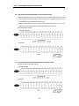
1) The following shows analog output states according to various
settings of functions that control analog output. When setting an
output state, be cautious for safety.
Channel Setting
Channel Specification
State
Used
Unused
A D/A conversion
PLC CPU in RUN state.
value is output.
PLC CPU in STOP state
A value of the speciPLC CPU in Error state
fied output state will
Voltage:
be output.
0V
0: Median value of the
Current:
Communication error of
output range
12 mA
the remote I/O station
1: Previous value
(When loaded on the 2: Max. value of the
remote I/O station)
output range
3: Min. value of the
output range
2) Sometimes, fault of output device or internal circuit can make
output abnormal. Design a supervising circuit in the outside for
output signals which can cause serious accidents.
!
CAUTION
▶ Do not run I/O
signal lines near
to high voltage
line or power line.
Separate them as
100 mm or more
as possible. Otherwise, noise can
cause
module
malfunction .
Installation Precautions
!
Wiring Precautions
!
CAUTION
▶ Operate the PLC in the environment conditions given in the
general specifications.
▶ If operated in other environment
not specified in the general
specifications, it can cause an
electric shock, a fire, malfunction
or damage or degradation of the
module
▶ Make sure the module fixing
projections is inserted into the
module fixing hole and fixed.
▶ Improper installation of the module can cause malfunction, dis order or falling.
CAUTION
▶ When grounding a FG terminal,
be sure to provide class 3
grounding which is dedicated to
the PLC.
▶ Before the PLC wiring, be sure to
check the rated voltage and terminal arrangement for the module and observe them correctly.
If a different power, not of the
rated voltage, is applied or
wrong wiring is provided, it can
cause a fire or disorder of the
nodule.
▶ Drive the terminal screws firmly
to the defined torque.
If loosely driven, it can cause
short circuit, a fire or malfunction.
▶ Be careful that any foreign matter
like wire scraps should not enter
into the module.
It can cause a fire, disorder or
malfunction.
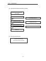
Test Run and Maintenance
Precautions
!
!
WARNING
▶ Do not contact the terminals
while the power is applied.
It can cause malfunction.
▶ When cleaning or driving a terminal screw, perform them after the
power has been turned off
▶ Do not perform works while the
power is applied, which can
cause disorder or malfunction.
CAUTION
▶ Do not separate the module from
the printed circuit board(PCB), or
do not remodel the module.
They can cause disorder, malfunction, and damage of the
module or a fire.
When mounting or dismounting
the module, perform them after
the power has been turned off.
▶ Do not perform works while the
power is applied, which can
cause disorder or malfunction.
Waste Disposal Precautions
!
CAUTION
▶ When disposing the module, do it as an industrial waste.
◎ CONTENTS ◎
Chapter 1. INTRODUCTION
1.1
1.2
Features
············································································································································1 - 1
1.1.1
G3F-DA4V G3F-DA4I ···················································································································1 - 1
1.1.2
G4F-DA1A·····································································································································1 - 1
Glossary
1.2.1
············································································································································1 - 2
A-Analog Value ·····························································································································1 - 2
1.2.2
D-Digital Value ····························································································································1 - 2
1.2 3
Digital/Analog C onversion Characteristics ···················································································1 - 3
Chapter 2. SPECIFICATIONS
2.1
General Specifications
····················································································································2 - 1
2.2
Performance Specifications················································································································2 - 2
2.3 Names of Parts and Functions ·······································································································2 - 3
2.3.1
G3F-DA4V / G3F-DA4I ···············································································································2 - 3
2.3.2
G4F-DA1A
································································································································2 - 5
2.4
External Power Supply ( ± 15 VDC Specifications)
2.5
I/O Conversion Characteristics···········································································································2 - 7
······································································2 - 6
2.5.1
Offset/Gain Value ························································································································2 - 7
2.5.2
Example for I/O Conversion Characteristic ················································································2 - 7
2.5.3
Relations between Offset/Gain Value and Analog Output ·························································2 - 8
2.5.4 I/O Conversion Characteristics According to the Offset/Gain Setting ········································2 - 9
1) Voltage Output Characteristics ··································································································2 - 9
2) Current Output Characteristics ·································································································2 - 11
2.6
D/A Conversion Speed
··················································································································2 - 12
2.7
Offset/ Gain S etting·····························································································································2 - 12
2.7.1
Notes on Setting O ffset/G ain Value ····························································································2 - 13
2.7.2
Procedures of Setting Offset/Gain
··························································································2 - 14
Chapter 3. INSTALLATION AND WIRING
3.1
3.2
Installation·············································································································································3 - 1
3.1.1
Installation A mbience····················································································································3 - 1
3.1.2
Installation Precautions·················································································································3 - 1
Wiring ··················································································································································3 - 2
3.2.1
Wiring Precautions ························································································································3 - 2
3.2.2
Wiring Examples
·······················································································································3 - 2
1) G3F-DA4V ·······································································································································3 - 2
2) G3F-DA4I ····································································································································3 - 3
3) G4F-DA1A ·······································································································································3 - 3
3.3
Wiring between the G3F-DA4I or the G3F-DA4V and DC 15V ·························································3 - 5
3.3.1
On Use of the G3F -PA1A or the G3F-PA2A ·················································································3 - 5
3.3.2
On Use of External Power Supply ······························································································3 - 6
Chapter 4. FUNCTION BLOCK
4.1 Insertion of the Function Block for the D/A Conversion Module on the GMWIN··························4 - 1
4.2
Local Function Block
······················································································································4 - 2
4.2.1 Module Initialization ··················································································································4 - 2
(G3F-DA4V / G3F-DA4I : DA4INI, G4F-DA1A : DA1INI)
4.2.2 Module Write_Array Type ···········································································································4 - 3
(G3F-DA4V / G3F-DA4I : DA4AWR, G4F-DA1A : DA1AWR)
4.2.3 Module Write_Single Type ············································································································4 - 4
(G3F-DA4V / G3F-DA4I : DA4WR, G4F-DA1A : DA1WR)
4.3
4.4
Remote Function Block ·····················································································································4 - 5
4.3.1
Module Initialization (G3F-DA4V / G3F-DA4I : DAR4INI, G4F-DA1A : DAR1INI)·······················4 - 5
4.3.2
Module Write (G 3F-DA4V / G3F-DA4I : DAR4WR, G4F-DA1A : DAR1WR)·······························4 - 6
Errors on Function Block····················································································································4 - 7
Chapter 5. GM PROGRAMMING
5.1
Programming for Controlling Inverter S peed with 5 Step Analog Output Voltage ·······················5 - 1
5.2
Programming for Displaying D/A Conversions which is S et by Digital Switch ··························5 - 6
5.3
Programming for Mounting D/A Conversion Module on Remote I/O Station ·····························5 - 9
Chapter 6. BUFFER MEMORY CONFIGURATION AND FUNCTION
6.1
6.2
Buffer Memory Configuration ···········································································································6 - 1
6.1.1
G3F-DA4V / G3F-DA4I ···············································································································6 - 1
6.1.2
G4F-DA1A
································································································································6 - 2
Buffer Memory Function······················································································································6 - 3
6.2.1
Available Channel Specification
·······························································································6 - 3
6.2.2
Data I nput Type Specification ·······································································································6 - 3
6.2.3
6.2.4
Digital Input ·································································································································6 - 4
Specification of CPU M odule's S top Condition or Disabled Channel's Output Condition············6 - 4
6.2.5
SET Data S pecification ···············································································································6 - 5
6.2.6
Channel Operation Data A rea ······································································································6 - 5
Chapter 7. SPECIAL MODULE COMMAND(BUFFER MEMORY READ/WRITE)
7.1
7.2
Local Command ···································································································································7 - 1
7.1.1
Buffer Memory Read- GET, GETP C ommand ············································································7 - 1
7.1.2
Buffer Memory Write- PUT, PUTP C ommand
··········································································7 - 2
Remote Command································································································································7 - 3
7.2.1
Buffer Memory Read- RGET ······································································································7 - 3
7.2.2
Buffer Memory Write- RPUT
····································································································7 – 4
Chapter 8. MK PROGRAMMING
8.1
Basic Programming
·························································································································8 - 1
8.1.1
G3F-DA4V / G3F- DA4I ················································································································8 - 1
8.1.2
G4F-DA1A
································································································································8 - 2
8. 2 Application Programming
···············································································································8 - 3
8.2.1
Programming for C ontrolling I nverter S peed with 5 S tep Analog O utput Voltage ·······················8 - 3
8.2.2
8.2.3
Programming for Displaying of D/A Conversions which is S et by Digital Switch ····················8 - 5
Programming for Mounting D/A Conversion M odule on Remote I/O S tation ····························8 - 7
Chapter 9. TROUBLESHOOTING
9.1
Error Code Indicated by RUN LED Flickering···················································································9 - 1
9.2
Troubleshooting Procedure················································································································9 - 1
9.2.1
RUN LED Flickering ····················································································································9 - 1
9.2.2
RUN LED O ff
9.2.3
Sudden D/A Output Value Change·······························································································9 - 3
····························································································································9 - 2
9.2.4
Digital and A nalog Value Mismatch ······························································································9 - 4
9.2.5
D/A Output Value Always deviates from Specified Value ·····························································9 - 5
9.2.6
Analog O utput Value A ccording to D/A I nput Value isn't Changed ··············································9 - 6
9.2.7
D/A Conversion Module H ardware Fault ····················································································9 - 6
Chapter 10. G3F-PA1A/G3F-PA2A POWER SUPPLY MODULE
10.1
Performance Specification ············································································································10 - 1
10.2
Notes on Handling ·························································································································10 - 2
10.3
Names of Parts ·······························································································································10 - 2
10.4
Dimensions ····································································································································10 – 3
Chapter 11. DIMENSIONS
11. 1
G3F-DA4V / G3F-DA4I Dimensions
11.2
G4F -DA1A Dimensions
·····························································································11 - 1
·················································································································11 - 2
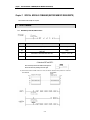
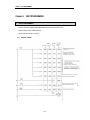
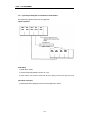
Chapter 1. INTRODUCION
Chapter 1.
INTRODUCTION
The G3F-DA4V, the G3F-DA4I and the G4F-DA1A are digital/analog conversion modules for use with the GLOFA
PLC GM 1/2/3/4 series CPU module and the MSTER-K300S/1000S series CPU module. The G4F-DA1A is used
on the GM4 series module and the K300S series module. the G3F-DA4V and the G3F-DA4I are used on the
GM1/2/3 series module and the K1000S series module. (Here-in-after the G4F -DA1A, G3F-DA4V and G3F-DA4I
are called the D/A conversion module)
The D/A conversion module is to convert a 16-bit, signed BIN digital value into an analog output signal (voltage or
current).
1.1 Features
1.1.1
G3F-DA4V / G3F- DA4I
1) Allows digital to Analog conversion for 16 channels per a module.
G3F-DA4V: 1 module can be performed for D/A conversion (voltage output) of 16 channels.
G3F-DA4I: 1 module can be performed for D/A conversion (current output) of 16 channels.
2) High resolution of 1/16000
A digital value resolution can be selected among 1/ 16000 and so the analog value of high resolution
is kept.
4) The number of the D/A conversion module mounted on one base is unlimited.
On use of power supply module of the G3F-PA1A or G3F-PA2A, the G3F-DA4V and G3F- DA4I can
be mounted up to 4.
1.1.2
G4F-DA1A
1) Allows digital to Analog conversion for 2 channels per a module.
1 module can be performed for D/A conversion (voltage or current output) of 2 channels.
2) High resolution of 1/16000
A digital value resolution can be selected among 1/ 16000 and the analog value of high resolution is
kept.
3) The number of the G4F-DA1A mounted on one base is unlimited.
1 -1
Chapter 1. INTRODUCION
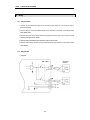
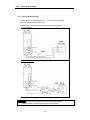
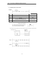
1.2 Glossary
A - Analog Value
Temperature
1.2.1
Temperature
0 ~ 1000°C
⇒
Transducer
⇒
-10 ~ 10V
voltage input to
A/D conversion
module
time
0
[Fig 1.2] Example of Transducer
[Fig 1.1] Analog Value
Analog value is a sequentially changing value such as voltage, current, temperature, speed, pressure,
flux, etc.
Temperature, for example, is sequentially changing according to the time. Because this temperature is
not input on the PLC directly, the same analog value of DC voltage (0 to ±10V) or current (4 to 20mA)
in accordance with the temperature should be input on the PLC through transducer.
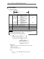
D - Digital Value
Number of man
1.2.2
Digital value is non-sequentially changing value written
as the number like 0, 1, 2, 3. The
signal of on or off is
written as digital value of 0 or 1. There are BCD value
and binary value in the range of digital value.
time
[Fig. 1.3] Digital quality
Analog value isn't written directly on the CPU. For
A/D
Conversion
CPU
(Digital
processing)
D/A
Conversion
analog input to the CPU operation, analog converted
to digital value has to be input on the CPU. and for
analog output, the digital of CPU should be
converted to analog.
Analog
0~±10V or
4~20mA
Analog
0~±10V or
4~20mA
[Fig. 1.4] conversion processing
in the PLC
1 -2
Chapter 1. INTRODUCION
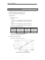
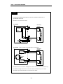
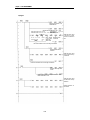
1.2.3
Digital/ Analog Conversion Characteristics
1) Voltage output
Analog
output
voltage
Analog
output
voltage
[Fig 1.5] D/A conversion characteristics(Voltage output)
Digital/analog conversion module allows digital value of the CPU to be converted into an analog value
and to be output externally. Digital input v alue of 0 leads to analog output value of -10V and 16000
leads to 10V. Digital input value of 1 is equal to 1.25mV.
2) Current output
Analog
output
current
Analog
output
current
[Fig 1.6] D/A conversion characteristics(Current output)
On current output, digital value of 0 is to be converted into 4mA and 16000. into 20mA. Digital input of 1
is equal to 1㎂.
1 -3
Chapter 2. SPECIFICATIONS
Chapter 2.
SPECIFICATIONS
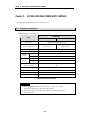
2.1 General Specifications
Table 2.1 shows the common specifications of GLOFA GM series and MASTER-K series
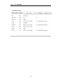
No
1
2
3
4
Items
Reference
Specification
Specifications
Operating ambient
temperature
Storage ambient
temperature
0 ~ 55℃
-25 ~ 75℃
Operating ambient
humidity
Storage ambient
humidity
5 ~ 95%RH, non-condensing
5 ~ 95%RH,
non-condensing
Occasional vibration
Frequency
5
Vibration
6
Shocks
7
8
9
10
11
Noise immunity
Operating
atmosphere
Altitude for use
Pollution degree
Cooling method
Acceleration
Amplitude
Sweep count
0.075mm
9.8 m/s 2 {1G}
10 times in
Continuous vibration
each direction
Frequency
Acceleration
Amplitude
for X, Y, Z
0.035mm
10≤f∠57 Hz
57≤f≤150 Hz 4.9 m/s 2 {0.5G}
•Maximum shock acceleration: 147 m/s2 {15G}
•Duration time :11ms
•Pulse wave: half sine wave pulse( 3 times in each of X, Y and Z directions )
10≤f∠57 Hz
57 ≤f≤150 Hz
Square wave impulse noise
±1,500 V
Electrostatic discharge
Voltage :4kV(contact discharge)
Radiated
electromagnetic field
27 to 500 MHz, 10V/m
Severity
Level
All power
modules
Digital
Digital I/Os
I/Os(U (Ue < 24 V)
Analog/Os
e≥
Fast transient /burst noise
24 V) communication
I/Os
Voltage
2kV
1kV
0.25kV
Free from corrosive gases and excessive dust
IEC 61131-2
IEC 61131-2
IEC 61131-2
IEC 1000-4-2
IEC 61131-2
IEC 1000-4-3
IEC 61131-2
IEC 1000-4-4
Up to 2,000m
2 or lower
Self-cooling
[Table 2.1 ] General Specifications
REMARK
1) IEC(International Electrotechnical Commission)
:The international civilian organization which produces standards for electrical and electronics industry..
2) Pollution degree
:It indicates a standard of operating ambient pollution level.
The pollution degree 2 means the condition in which only non conductive pollution occurs. Occasionally,
however, a temporary conductivity caused by condensation shall be expected.
2 -1
Chapter 2. SPECIFICATIONS
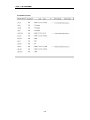
2.2 Performance Specifications
Table 2..2 shows performance specification of D/A conversion module.
Items
Specifications
G3F-DA4I
G3F-DA4V
I/O points
Digital input
Analog output
Max. resolution
16points
• 16bit(data part :14bits)signed binary
• May be set per channel by setting input data.("0" : -192~16191, "1" : -8192~-8191)
DC 4~20mA
(External load resistance
less than 510Ω)
-5~5 VDC
(External load resistance :2KΩ~
1MΩ)
-10~10 VDC
(External load resistance :2KΩ~
1MΩ)
-5~5 VDC
(External load resistance :
2KΩ~1MΩ)
DC-4~20 mA
(External l oad resistance less
than550Ω)
1μA(1/16000)
-5~5 VDC
0.625 mV(1/16000)
-10~10 VDC
1.25 mV(1/16000)
-10~10 VDC
1.25mV(1/16000)
DC4~20 mA:
1μA(1/16000)
Accuracy
Max. conversion
speed (ms/channel)
Max. absolute input
Analog output points
Isolation
Terminals connected
consumption
Internal current
ccconsumption
Voltage
External
power supply Current
Weight
G4F-DA1A
± 0.3% [Full Scale]
15ms/ 16 channels
DC 24mA
3ms/ 2 channels
Voltage: 15 VDC
Current:DC 24 mA
16 channels/1module
2channels/1module
Between input terminals and the PLC: Photo-coupler isolation
15 VDC
38-point terminal block
20-point terminal block
0.25 A
15 VDC / - 15 VDC
0.45 A
15 VDC : 0.5 A
-15 VDC : 0.1 A
15 VDC :0.5 A
-15 VDC :0.3 A
-
610 g
630 g
370 g
[Table 2.2] Performance Specifications
2 -2
Chapter 2. SPECIFICATIONS
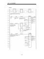
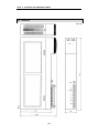
2.3 Names of Parts and Functions
Names of parts and functions are shown as below.
2.3.1
G3F-DA4V / G3F-DA4I
②
④
⑤
4~20mA
2 -3
Chapter 2. SPECIFICATIONS
No.
Descriptions
①
RUN LED
Indicates the operating condition of the D/A conversion module
* On: Normal operation
* Flickering: An error has occurred. (For more information, see the Section 6.1)
* Off : 5 VDC power off or D/A conversion module fault
②
Channel select switch
Used to set the channel of the adjustment of offset/gain in the test mode.
Setting range: 0~F
③
Offset/gain select switch
Used to select Offset/Set/Gain .
*Offset position: offset value adjustment mode
*Gain position: gain value adjustment mode
*Set position: the mode which stores offset/gain value.
(When the switch is changed to "set" position from "Offset/ Gain" position, offset/gain value
is stored in the memory of D/A conversion module.)
④
Up/Down switch
-Used to make micro adjustment of offset/gain value.
-Analog output value according to up/down location is changed as follows.:
*Up/down location of less than 2 sec :
G3F-DA4I - Add or fall of 1㎂/1 time
G3F-DA4V-Add or fall of 1.25 mV/1 time
*Up/down location of more than 2 sec :
G3F-DA4I-Add or fall of 10㎂/ 0.2 sec.
G3F-DA4V Add or fall of 12.5 mV/0.2 sec
⑤
Test terminal block
Test mode is to be a connection of terminal block 1 and 2
Normal mode is to be a disconnection of terminal block 1 and 2
Output range select switch
It's only for the G3F-DA4V.
⑥
*Factory set is made to -10~10 VDC.
2 -4
Chapter 2. SPECIFICATIONS
2.3.2
G4F-DA1A
No.
Descriptions
RUN LED
Indicates the operating status the G4F-DA1A
*Normal mode
-On: Normal operation
-Flicker: error occurring
①
-Off: 5 VDC power off or the G4F-DA1A module fault.
*Test mode
-Flicker(per 1.0 sec): Offset/G ain select switch is set to offset
condition or gain condition.
-Off: offset/gain select switch is set to Set condition.
Offset/ Set/Gain select switch
②
*Offset position: Offset value control mode
*Gain position: Gain value control mode
*Set position: Offset/ Gain value set mode
(When offset/gain position is changed to set position,
offset/gain value is stored onto G4F-DA1A buffer
memory.)
Channel select switch
③
Used to select channel for adjusting offset/gain value on test mode.
*CH0: enabled to adjust the offset/gain value on the CH0
*Neutral: disabled to adjust the offset/gain value
*CH1 :enabled to adjust the offset/gain value on the CH1.
Up/ Down switch
-Used to make micro adjustment of offset/gain value.
-Analog output value according to up/down location is changed as
follows.:
④ *Up/Down location of less than 2 sec Add or fall of 1.25mA(voltage)
Add or fall of 1.0μA(current)
*Up/Down location of more than 2 sec Add or fall of
12.5mA(voltage)
Add or fall of 10μA(current)
Test terminal block
⑤ Test mode is to be a connection of terminal block 1 and 3
Normal mode is to be a disconnection of terminal block 1 and 3
2 -5
Chapter 2. SPECIFICATIONS
2.4 External Power Supply( ± 15 VDC Specifications)
Be sure to use rated power supply on the table 2. 3 when power(±15 VDC) is supplied to D/A conversion
module for use with the GLOFA PLC GM1/2/3 series and the MASTER-K1000S series .
Specifications
Item
G3F-DA4I
+15VDC ± 3%(14.55 V~15.45 V)
Voltage
*1
Current consumption
G3F-DA4V
-15 VDC ± 3%(-15.45 V~-14.55 V)
+15 VDC
0.5 A
0.5 A
-15 VDC
0.1 A
0.3 A
Ripple voltage
less than 50 mV p-p
Spike voltage
less than 100 mVp-p
transient output change
less than ± 1 V
[Table 2.3] External power supply specifications
*1: Current consumption shown on the above table 2.3 is applicable to a piece of D/A conversion module.
2 -6
Chapter 2. SPECIFICATIONS
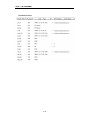
2.5 Input/Output Conversion Characteristics
I/O characteristics are displayed as a slant of the line connecting offset value and gain value in converting an
digital signal from the external PLC into an analog signal(voltage or current).
The I/O conversion characteristics of the D/A conversion module are shown.
2.5.1 Offset/ Gain Value
1) Offset and gain value is as follows
a) Offset value
Data format of -8192~8191: When digital input value is -8000, offset value is analog output value.
Data format of -192~16191: When digital input value is 0, offset value is analog output value.
b) Gain value
Data format of -8192~8191: When digital input value is 0, offset value is analog output value.
Data format of -192~16191: When digital input value is 8000, offset value is analog output value.
2) Factory set value of offset and gain value is like table 2.4.
Module name
Analog input range
Offset value
Gain value
G3F-DA4I
DC 4~20 mA
DC 4 mA
DC 12 mA
G3F-DA4V
-10 ~10 VDC
-10 VDC
0 VDC
G3F-DA1A
-10 ~10 VDC
-10 VDC
0 VDC
[Table 2.4] Factory set value of offset and gain
3) Offset and gain value can be selected per channel on test mode.
2.5.2
Example for I/O Conversion Characteristic.
Input/ output conversion characteristic example is shown on Fig 2.1
[Fig 2.1] Input/ output conversion characteristic example
2 -7
Chapter 2. SPECIFICATIONS
2.5.3 Relations between Offset/ Gain Value and Analog Output
The resolution of D/A conversion module can be changed by changing offset/ gain value. At the change of
offset/ gain value, the below formula can calculate resolution of analog value and analog output value by
digital input value.
Resolution
=
Analog output
=
Analog output
=
Gain value - Offset value
8000
Gain value
- Offset value
8000
Resolution
Ex) Gain value : 0 VDC
5
Digital input value 5
Offset value : - 10 VDC
5 Digital input value +Offset value
Offset value
Digital input value : 12000
0 – ( - 10 )
Resolution
=
= 0.00125
8000
Analog output = 0.00125 5 12000 +(- 10) = 5(V)
Since maximum resolution of D/A conversion module is like values on table2.5, if digital input value increase
or decrease one at a time, analog output value may be different with a result of above formula
Product code
Analog output range
Maximum resolution
G3F-DA4I
DC 4~20 mA
1μA
-10 ~10 VDC
1.25 mV
-5 ~5 VDC
0.625 mV
DC 4~20 mA
1μA
-10 ~10 VDC
1.25 mV
G3F-DA4V
G4F-DA1A
[Table 2.5] Maximum resolution
2 -8
Chapter 2. SPECIFICATIONS
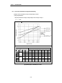
I/O Conversion Characteristics according to Offset/ Gain Setting
Input/output conversion characteristics according to offset/ gain setting are as below.
1) Voltage output characteristics
Voltage output characteristics according to offset/ gain setting are shown in the Fig2.2 and Fig2.3.
(1) -10 ~10 VDC
-10 ~10 VDC
Analog output voltage
2.5.4
No
Digital
Input
range
Offset
value
Gain
value
-8000
-4000
0
4000
8000
12000
16000
-192
~
16191
0V
5V
-
-
0V
2.5 V
5V
7.5 V
10 V
-5 V
0V
-
-
-5 V
-2.5 V
0V
2.5 V
5V
-10 V
0V
-
-
-10 V
-5 V
0V
5V
10 V
0V
5V
0V
2.5 V
5V
7.5 V
10 V
-
-
-5 V
0V
-5 V
-2.5 V
0V
2.5 V
5V
-
-
-10 V
0V
-10 V
-5 V
0V
5V
10 V
-
-
-8192
~
8191
Digital input value
[Fig 2.2] Voltage output characteristics(-10 ~ 10 VDC)
2 -9
Chapter 2. SPECIFICATIONS
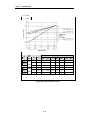
(2) -5 ~ 5 VDC
Analog output voltage
-5 ~5 VDC
No
Digital
Input
range
Offset
value
Gain
value
-8000
-4000
0
4000
8000
12000
16000
-192
~
16191
1V
3V
-
-
1V
2V
3V
4V
5V
0V
2.5 V
-
-
0V
1.25V
2.5 V
3.75V
5V
-5 V
0V
-
-
-5 V
-2.5 V
0V
2.5 V
5V
0V
3V
1V
2V
3V
4V
5V
-
-
1V
2.5 V
0V
1.25V
2.5 V
3.75V
5V
-
-
-5 V
0V
-5 V
-2.5 V
0V
2.5 V
5V
-
-
-8192
~
8191
Digital input value
[Fig 2.3] Voltage output characteristics(-5 ~ 5 VDC)
2 - 10
Chapter 2. SPECIFICATIONS
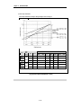
2) Current output characteristics
Current output characteristics according to offset/ gain setting are shown in the Fig2.4.
DC 4 ~20 mA
No
Digital
Input
range
-192
~
16191
-8192
~
8191
Offset
value
Gain
value
10 mA
Digital input value
-8000
-4000
0
4000
8000
12000
16000
15 mA
-
-
10 mA
12.5mA
15 mA
17.5mA
20 mA
6 mA
10 mA
-
-
6 mA
8 mA
10 mA
12 mA
14 mA
4 mA
12 mA
-
-
4 mA
8 mA
12 mA
16 mA
20 mA
10 mA
15 mA
10 mA
12.5mA
15 mA
17.5mA
20 mA
-
-
6 mA
10 mA
6 mA
8 mA
10 mA
12 mA
14 mA
-
-
4 mA
12 mA
4 mA
8 mA
12 mA
16 mA
20 mA
-
-
[Fig 2.4] Current output characteristics(DC 4 ~ 20 mA)
2 - 11
Chapter 2. SPECIFICATIONS
2.6 D/A Conversion Speed
Conversion speed indicates the period of time between D/A conversion processing and changing analog value
to Set value.
Conversion speed of each D/A conversion module is like value in the table 2.6.
Products
Conversion speed
G3F-DA4I
15 ms/ All channel
G3F-DA4V
15 ms/ All channel
G4F-DA1A
3 ms/ All channel
[Table 2.6] Conversion Speed
That is, conversion speed of each D/A conversion module is constant regardless of used channels.
2.7 Offset/ Gain Setting
- Factory set to offset/ gain value is set like below table 2.7
Products
Analog output range
Offset value
Gain value
G3F-DA4I
DC 4-20 mA
DC 4 mA
DC 12 mA
G3F-DA4V
-10~10VDC
-10 VDC
0 VDC
G4F-DA1A
-10~10 VDC
-10 VDC
0 VDC
[Table 2.7] Factory set to offset and gain value
- The setting change and micro adjustment of offset/ gain value is executed on test mode.
2 - 12
Chapter 2. SPECIFICATIONS
2.7.1 Notes on Setting Offset/ Gain Value
1) Don't make D/A conversion processing on test mode.
D/A conversion processing on test mode allows D/A conversion of every channel to be stopped and
external device not to be controlled regularly.
If test mode is changed to normal mode, D/A conversion restarts with new offset/gain value.
2) Offset/ gain setting has to be set in the range of below.
a) Voltage output range of 10 V is applicable to -10~0~10 V
b) Voltage output range of 5 V is applicable to -5V~0~5 V
c) Voltage output range of 20 mA is applicable to 4~12 mA.
The setting exceeding the above range doesn't keep accuracy from being within the range of the
performance specification.
3) When offset/gain select switch is located on "Set" position, set value of offset/gain is stored.
When offset/gain select switch is located on "offset" or "gain" position, the end of test mode allows
offset/gain value to remain previous value.
4) Change the channel setting offset/ gain value after offset/gain select switch is located on "Set" position.
If channel change is made on offset/gain select switch of "offset" or "gain” position, and set offset/gain
select switch is set on "Set" position on the other channel, offset/gain value is stored on first channel
which would be changed.
REMARK
1) When gain value of channel 3 is changed from 10 to 5 Volts, and offset/gain select switch is
located on "gain" position, channel change to 4 allows gain value to be like next.
(1)Gain value of channel 3 : 5 Votls is output.
(2)Gain value of channel 4 : Previous value is output.
-When offset /gain select switch is set to "Set" position, gain value is stored as 5 Volts on
channel 3 and previous value remains on channel 4.
5) When the range exceeds possible offset/gain setting range, "RUN" LED flickers at high speed (interval
time: 0.1 sec). When LED display writes Err 4 and "RUN" LED display flickers at high speed, readjust
offset/gain within possible offset/gain setting range, offset/gain value is operated regularly and LED display
indicates test mode.
2 - 13
Chapter 2. SPECIFICATIONS
2.7.2 Procedure of Setting Offset/ Gain
Offset/ Gain setting procedure is shown as below.
Offset/ Gain value is adjusted for each channel.
Make a connect of Test terminal blocks
Test mode condition
G3F-DA4 V/G3F-DA4I: test terminal block 1 and 2. G4F-DA1A : test terminal block 1 and
3.:RUN LED- Off
Make sure that offset/gain switch is set to "Set" position and set channel for adjusting
offset/gain by channel select switch.
Analog output channel
setting
Connect the instrumentation syste m to channel for adjusting offset/gain
Connect instrumentation
system
Locate offset/gain switch on "offset" position. RUN LED flickers (per 0.1 sec)
Adjust output value in accordance with offset value by up/own switch .:RUN LED flickers
Offset value adjustment
(per 0.1 sec)
Locate offset/Set/gain on "Set" position. :RUN LED Off
Locate offset/Set/gain on "gain" position :RUN LED flickers (per 1.0 sec)
Adjust output value in accordance with gain value by up/down switch .:RUN LED flickers
( per 0.1 sec)
Locate offset/Set/gain on "Set" position. RUN LED: Off
No
Adjust enabled channel completely?
Yes
Make no connection of Test terminal blocks
(G3F-DA4V/G3F-DA4I: Terminal block 1, 2. G4F-DA1A: terminal block 1, 3)
Completed
2 - 14
Gain value adjustment
Chapter 3. INSTALLATION AND WIRING
CHAPTER 3. INSTALLATION AND WIRING
3.1 Installation
3.1.1 Installation Ambience
This module has high reliability regardless of its installation ambience. But check the following for system in
higher reliability and stability.
1) Ambience requirements
Avoid installing this unit in locations which are subjected or exposed to :
- Water leakage and a large amount of dust, power and other conductive powder, oil mist, salt, of
organic solvent
- Mechanical vibrations of impacts transmitted directly to the module body
- Direct sunlight.
- Dew condensation due to sudden temperature change.
- High or low temperatures (outside the range of 0-55°C)
2) Installation and wiring
- During wiring or other work, do not allow any wire scraps to enter into the PLC.
- Install it on locations that are convenient for operation.
- Make sure that it is not located near high voltage equipment on the same panel.
- Make sure that the distance from the walls of duct and external equipment be 50 mm or more.
- Be sure to be grounded to locations that have good noise immunity.
3.1.2 Installation Precautions
From unpacking to installation of the D/A conversion module, be sure to check the following:
1) Do not drop it off, and make sure that strong impacts should not be applied.
2) Do not dismount printed circuit board(PCB) from the case. It can cause malfunctions.
3) During wiring, be sure to check any foreign matter like wire scraps should not enter into the upper
side of the PLC, and in the event that foreign matte entered into it, always eliminate it.
4) Be sure to disconnect electrical power before mounting or dismounting the module.
3 -1
Chapter 3. INSTALLATION AND WIRING
3.2 Wiring
3.2.1
Wiring Precautions
1) Separate AC and external input signal of D/A conversion module wiring not to be affected by surge or
induced noise in the AC.
2) External wiring has to be at least AWG22(0.3 ㎟) and be selected in consideration of operating ambience
and/or allowable current.
3) Separate wiring from devices and/or substances generating intense heat, and oil not to make short-circuit
which leads to damage and/or mis -operation.
4) Identify the polarity of terminal block before external power supply is made connected.
5) Separate external wiring sufficiently from high voltage and power supply cable not to cause induced failure
and/or malfunction.
3.2.2
Wiring Examples
1) G3F-DA4V
Motor driving
module etc.
3 -2
Chapter 3. INSTALLATION AND WIRING
2) G3F-DA4I
Motor driving
module etc.
3) G4F-DA1A
Motor driving
module etc.
Current
output
*1 For the cable, use a two-core twisted shielded wire.
3 -3
Chapter 3. INSTALLATION AND WIRING
Remark
▶ Current output module(G3F-DA4I, G4F-DA1A) cannot be connected with device which i s
grounded with common line.
Because it is not normal current output.
1) G3F-DA4I
Motor driving
module etc.
CH 0
3
4
D/A converter
curcuit
CH F
33
34
+15V
AGND
36
37
38
-15V
DC +15V
0V
DC -15V
2) G4F-DA1A (when it is used to current output type for 2 channel all)
Motor driving
module etc.
CH 0
D/A converter
circuit
Vcc
+5V
+15V
0V
GND -15V
5
7
+15V
AGND
-15V
CH 1
D/A converter
circuit
17
19
▶ The G4F-DA1A is not used to voltage and current in the one channel simultaneously.
If it is used to voltage and current in the one channel simultaneously, it is caused
abnormal output and malfunction for internal circuit failure
3 -4
Chapter 3. INSTALLATION AND WIRING
3.3 Connection of G3F-DA4I/ G3F-DA4V and ± 15 VDC
There are two ways which ±15 VDC is supplied to G3F-DA4I or G3F-DA4V.
1) When the G3F-PA1A or G3F-PA2A is used,.
; G3F- PA1A : power supply module for the 110 VAC
; G3F- PA2A : power supply module for the 220 VAC
2) When the external power supply is used,.
3.3.1 On Use of the G3F-PA1A or G3F-PA2A.
- When the G3F-PA1A or G3F-PA2A (Here-in-after called the power supply module for the D/A conversion)
is used, connect the D/A conversion module and each part of +15, 0, -15 VDC of power supply module for
the D/A conversion.
- One power supply module for the D/A conversion is performed to supply power up to 4 D/A conversion
module in block.
Connection of G3F - DA4V / G3F - DA4I and ± 15 VDC
-
Don't put the parallel connecti on of ± 15 VDC output from several power supply modules for the D/A
conversion into one D/A conversion module. For it can make the power supply module for the D/A
conversion be damaged.
3 -5
Chapter 3. INSTALLATION AND WIRING
3.3.2 On Use of the External Power Supply.
- Connect the D/A conversion module and the each part of
15, 0, -15 VDC of external power supply.
- Recommend a noise filter for the D/A conversion module.
- For the rated power of ±15 VDC for the D/A conversion module, refer to the General Remarks 2.4.
Use of no noise filter
Use of noise filter
REMARK
1) Separate the connection of noise filter and the D/A conversion module with the other wiring.
2) Make the connection of noise filter and the D/A conversion module in short distance.
3 -6
Chapter 4. FUNCITION BLOCK
Chapter 4. FUNCTION BLOCK
This chapter shows function block for the D/A conversion module on the GMWIN.
A kind of function block is as follows
NO.
G3F-DA4V, G3F-DA4I
G4F-DA1A
Function
Local
Remote
Local
Remote
1
DA4INI
DAR4INI
DA1INI
DAR1INI
Module initialization
2
DA4AWR
DAR4WR
DA1AWR
DAR1WR
Writing D/A conversion (Array type)
3
DA4WR
-
DA1WR
-
Writing D/A conversion (Single type)
REMARK
Function block of the G3F-DA4V and G3F-DA4I are same
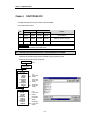
4.1 Insertion of the Function Block for D/A Conversion Module on the GMWIN
A function block can be inserted during the execution of the GMWIN according to the following procedure..
A function block can be inserted only when a project opens.
Project(P)
Select
Library insert(I)
G3F – DA4V,
G3F – DA4I
1. Special.3fb
. DA4INI
. DA4AWR
. DA4WR
2. Remote3.3fb
. DAR4INI
. DAR4WR
3. Remote4.3fb
. DAR1INI
. DAR1WR
G4F – DA1A
1. Special.4fb
. DA1INI
. DA1AWR
. DA1WR
2. Remote4.4fb
. DAR1INI
. DAR1WR
3. Remote3.4fb
. DAR4INI
. DAR4WR
Local
Function block
Inserting
Remote GM3
Function block
Inserting
Remote GM4
Function block
Inserting
Local
Function block
Inserting
Remote GM4
Function block
Inserting
Remote GM3
Function block
Inserting
4 -1
Chapter 4. FUNCITION BLOCK
4.2 Local Function Block
4.2.1
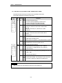
Module Initialization (G3F-DA4V/G3F-DA4I : DA4INI, G4F-DA1A : DA1INI)
A module initialization function block is a program for the use in setting a D/A conversion module base location, the
slot location number, specifying an available channel enable, a data type for D/A conversion, and output continuing
data for D/A conversion when the CPU module stops.
Function
Data
I/O Variable
Descriptions
Block
type
Input
REQ
BOOL Function Block Execution Request Area
-The execution of function block initialization is requested in this area.
-If the status connected with this area is satisfied on the programexecution and 0 is changed to
1, function block initialization for the module is executed.
Output
BASE
USINT
Base Location Number Area
-The base No. on which D/A conversion module is mounted is written on this area.
-Setting range : GM1 series( 0 to 31 ), GM2 series( 0 to 7), GM3/4 series( 0 to 3)
SLOT
USINT
CH
BOOL
[Array]
Slot Location Number Area
-The slot No. on which D/A conversion module is mounted is written on this area.
-Setting range: 0 to 7
Available Channel Specification Area
-Available channels are specified in this area.
DATA
TYPE
BOOL
[Array]
SEL
USINT
[Array]
DONE
BOOL
STAT
USINT
ACT
BOOL
[Array]
* Note 1
-Enabled channels are specified to 1 and disabled channels are specified to 0.
Input Data Type Specification Area
-Input digital data type for each channel is specified in this area.
-0 is for the range of -192 to 16191.
-1 is for the range of -8192 to 8191.
When a CPU module stops or channel is disabled, output value is specified in this area.
-"0" leads to output the medium value of the range.
-"1" leads to output the previous value.
-"2" leads to output the maximum value of the range.
-"3" leads to output th e minimum value of the range.
Function Block Execution Complete Area
-When function block initialization has been completed with no error, 1 is written and until next
execution, 1 is continuing. When error occurs, 0 is written and operation comes to stop.
Error Code Display Area
-When error occurs during function block processin g, the error code number is written.
-For error code, refer to Section 7.4.
Channel Operation Display Area
-Enabled channel specified after executing the function block initialization with no error is normal,
1 is written and, 0 is written to the non-specified channel.
REMARK
*Note 1 :The number of Array are the G3F-DA4V and G3F-DA4I of 16 and the G4F-DA1A of 2
4 -2
Chapter 4. FUNCITION BLOCK
4.2.2
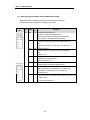
Module Write_ Array Type (G3F-DA4V / G3F-DA4I : DA4AWR, G4F-DA1A : DA1AWR)
Module write function block of the Array type is a program for the use in performing for every channel in
block and setting a digital value to be converted into a D/A conversion.
Function
Block
I/O
Variable
input
REQ
Descriptions
BOOL Function Block Execution Request Area
-The execution of function block initialization is requested in this area.
-If the status connected with this area is satisfied on the program
execution and 0 is changed to 1, function block for the module is
executed.
BASE USINT Base
Location Number Area
-The base No. on which D/A conversion module is mounted is written on
this area.
-Setting range : GM1 series( 0 to 31 ), GM2 series( 0 to 7), GM3/4
series( 0 to 3)
SLOT USINT Slot Location Number Area
-The slot No. on which D/A conversion module is mounted is written on
this area.
-Setting range: 0 to 7
CH BOOL Available Channel Specification Area
[Array] -Available channels are specified in this area.
*Note1
-Enabled channels are specified to 1 and disabled channels are specified
DATA
output
Data
Type
INT Input Data Type Specification Area
[Array] -Input digital data type for each channel is specified in this area.
*Note1
DONE BOOL Function Block Execution Complete Area
- When function block has been completed with no error, 1 is written and
until next execution, 1 is continuing. When error occurs, 0 is written and
operation come to stop.
STAT USINT Error Code Display Area
- When error occurs during function block processing, the error code
number is written.
- For error code, refer to Section 4.4.
ACT
BOOL Channel Operation Display Area
[Array] - Enabled channel specified after executing the function block with no
*Note1 error is normal, 1 is written and, 0 is written to the non-specified channel.
REMARK
* Note 1: The number of Array are the G3F-DA4V and G3F-DA4I of 16 and the G4F-DA1A of 2
4 -3
Chapter 4. FUNCITION BLOCK
4.2.3
Module Write_Single Type(G3F-DA4V / G3F-DA4I : DA4WR, G4F-DA1A : DA1WR)
Module write function block of the Single type is a program for the use in performing for a channel of D/A
conversion module and setting a digital value to be converted into a D/A conversion.
Function
block
I/O
Variable
input
REQ
BASE
SLOT
CH
Data
type
Descriptions
BOOL Function Block Execution Request Area
-The execution of function block is requested in this area.
- If the status connected with this area is satisfied on the program execution
and 0 is changed to 1, function block for the module is executed.
USINT Base Location Number Area
- The base No. on which D/A conversion module is mounted is written on this
area.
- Setting range : GM1 series( 0 to 31 ), GM2 series( 0 to 7), GM3/4 series( 0
to 3)
USINT Slot Location Number Area
- The slot No. on which D/A conversion module is mounted is written on this
area.
- Setting range: 0 to 7
USINT Available Channel Specification Area
- Available channels are specified in this area.
DATA
output
DONE
STAT
INT
-Range:0~15(G4F-DA1A : 0~1)
Input Data Type Specification Area
- Input digital data type for each channel is specified in this area.
BOOL Function Block Execution Complete Area
- When function block has been completed with no error, 1 is written and until
next execution, 1 is continuing. When error occurs, 0 is written and
operation come to stop.
USINT Error Code Display Area
- When error occurs during function block processing, the error code
number is written.
- For error code, refer to Section 4.4.
4 -4
Chapter 4. FUNCITION BLOCK
4.3 Remote Function Block
4.3.1
Module Initialization(G3F-DA4V / G3F-DA4I : DAR4INI, G4F-DA1A : DAR1INI)
A module initialization function block is a program for the use in setting the location number of the slot on
which the communication module of the master station is mounted, the address number of communication
module which is ba sed on a remote I/O station, the base location number, and the slot location number, and
specifying the available channel enable, a data type for D/A conversion, and D/A conversion module condition
when the CPU module is stopping
Function
block
I/O
Variable
input
REQ
Data
Descriptions
type
BOOL Function Block Execution Request Area at arising edge
NET-NO USINT
ST_NO USINT
BASE
USINT Base Location Number Area
SLOT
USINT
CH
BOOL
[Array]
*Note 1
DATA
TYPE
BOOL
[Array]
SEL
USINT
[Array]
*Note 1
*Note 1
output
-The execution of function block initialization is requested in this area.
-If the status connected with this area is satisfied on the program execution and 0 is changed to 1,
function block initialization for the module is executed.
Slot Location Number Area
-The slot No. on which communication module of the master station is mounted is written on this
area. -Setting range: 0 to 7
The address number of communication module which is loaded on a remote I/O station.
-Setting range 0 to 63
-The base No. on which D/A conversion module is mounted is written on this area.
-Setting range : 0 to 3
Slot Location Number Area
-The slot No. on which D/A conversion module is mounted is written on this area. -Setting range:
0 to 7
Available Channel Specification Area
-Available channels are specified in this area.
-Enabled channels are specified to 1 and disabled channels are specified to 0.
Input Data Type Specification Area
-Input digital data type for each channel is specified in this area.
-0 is for the range of -192 to 16191.
-1 is for the range of -8192 to 8191.
When a CPU module stops or enabled channel is unused, output value is specified in this area.
-"0" leads to output the medium value of the range.
-"1" leads to output the previous value.
-"2" leads to output the maximum value of the range.
-"3" leads to output the minimum value of the range.
When function block initialization has been completed with no error, 1 is written and then next scan,
0 is written.
NDR
BOOL
ERR
BOOL Error Data Display Area
STAT
USINT
ACT
BOOL
[Array]
*Note 1
When error occurs during function block processing, 1 is written and operation comes to stop. On
the next scan, 0 is written.
Error Code Display Area
-When error occurs during function block processing, the errorcode number is written. - For error
code, refer to Section 7.4.
Channel Operation Display Area
-Enabled channel specified after executing the function block initialization with no error is normal, 1
is written and, 0 is written to the non-specified channel.
REMARK
* Note 1: The number of Array are the G3F-DA4V and G3F-DA4I of 16 and the G4F-DA1A of 2
4 -5
Chapter 4. FUNCITION BLOCK
4.3.2
Module Write (G3F-DA4V / G3F-DA4I : DAR4WR, G4F-DA1A : DAR1WR)
Module write function block of the Array type is a program for the use in performing for every channel in
block and setting a digital value to be converted into a D/A conversion.
Function
block
I/O
Vari able
input
REQ
Data
Descriptions
type
BOOL Function Block Execution Request Area at a rising edge.
-The execution of function block is requested in this area.
-If the status connected with this area is satisfied on the program execution and 0 is
changed to 1, function block for the module is executed.
NET_NO USINT -The slot No. on which the communication module of the master station is mounted
- Setting range: 0 to 7
ST_NO USINT The address number of communication module which is loaded on a remote I/O station.
- Setting range 0 to 63
BASE
USINT Base Location Number Area
SLOT
USINT Slot Location Number Area
CH
-The base No. on which D/A conversion module is mounted is written on this area.
-Setting range : 0 to 3
-The slot No. on which D/A conversion module is mounted is written on this area. Setting range: 0 to 7
BOOL Available Channel Specification Area
[Array] -Available channels are specified in this area.
*Note 1
DATA
-Enabled channels are specified to 1 and disabled channels are specified to 0.
INT Input Data Type Specification Area
[Array] -Input digital data type for each channel is specified in this area.
*Note 1
output
NDR
BOOL When function block has been completed with no error, 1 is written and then next scan,
0 is written.
Error Data Display Area
When error occurs during function block processing, 1 is written and operation comes
to stop. On the next scan, 0 is written.
ERR
BOOL
STAT
USINT Error Code Display Area
ACT
BOOL Channel Operation Display Area
[Array] -enabled channel specified after executing the function block initialization with no error
-When error occurs during function block processing, the error code number is written.
-For error code, refer to Section4.4.
*Note 1
is normal, 1 is written and, 0 is written to the non-specified channel.
REMARK
* Note 1 - The number of Array are the G3F-DA4V and G3F-DA4I of 16 and the G4F-DA1A of 2
4 -6
Chapter 4. FUNCITION BLOCK
4.4 Errors on Function Block
This shows the errors on the output variable “STAT” of variables and the resolutions in accordance with them.
STAT
No.
0
Local/
Remote
Local
1
2
Descriptions
Operating with no fault
The base location number is
exceeding the proper setting range
H/W error of the base
The slot location number is
exceeding the proper setting range
3
Function Block
Write
Initiali
Array Single
zation
type
type
O
O
O
O
O
O
O
O
O
O
O
O
Resolutions
Correct the number in accordance
with the proper range
(See Section 4.2)
Contact the service station.
Set the right number to the slot
mounting the D/A conversion module
4
The D/A conversion module on the
slot is empty
O
O
O
Mount the D/A conversion module to
the specified slot
5
The module loaded isn't the D/A
module
O
O
O
Mount the D/A conversion module to
the specified slot
6
The channel number is exceeding
the proper range
-
-
O
Specify the available channel
correctly
O
O
O
O
O
O
-
O
O
O
O
O
H/W error of the communication
module for remote
O
O
The base location number is
exceeding the proper setting range
O
O
Corsets the number in accordance
with the proper range
(See Section 4.2)
131
The slot location number is
exceeding the proper setting range
O
O
Set the right number to the slot
mounting the D/A conversion module
133
The module loaded isn't the D/A
module
O
O
Mount the D/A conversion module to
the specified slot
O
O
O
O
-
O
Make a correct specification of the
available channel on the initialization
function block
O
O
Transmit the test mode to normal
mode
H/W error of the D/A conversion
module
The D/A conversion module's
shared memory error
7
8
The available channels are not
specified
9
Test mode
10
128
129
135
136
137
138
Remote
H/W error of the D/A conversion
module
The D/A conversion module's
shared memory error
The available channels are not
specified
Test mode
4 -7
-
Contact the service station.
Contact the service station.
Make a correct specification of the
available channel on the initialization
function block
Transmit the test mode to normal
mode
See the manual for the remote
communication module
Contact the service station.
Contact the service station.
Chapter 5. GM PROGRAMMING
Chapter 5. GM PROGRAMMING
5.1 Programming for Controlling Inverter Speed with 5 Step Analog Output Voltage
1) System Configuration
2) Initial Settings
(1) Enabled channel : channel 0
(2) Data input type specification :channel 0(-192 ~16191)
(3) Output condition of D/A conversion module when the CPU is stopping : minimum value output of the range.
(4) Offset : 0 V Gain :5 V
3) Descriptions of the Program
(1) %I0.0.0 turning On leads to the initial setting of D/A conversion
(2) %I0.0.1 turning On leads to output of "0"(O V) on channel 0.
(3) %I0.0.2 turning On leads to output of "4000"(2.5 V) on channel 0
(4) %I0.0.3 turning On leads to output of "8000"(5 V) on channel 0.
(5) %I0.0.4 turning On leads to output of "12000"(7.5 V) on channel 0.
(6) %I0.0.5 turning On leads to output of "16000"(10 V) on channel 0.
5 -1
Chapter 5. GM PROGRAMMING
4) Program
Execution co ndition
Execution co ndition
Execution co ndition
Execution co ndition
Execution co ndition
5 -2
Chapter 5. GM PROGRAMMING
5) Initial Value Setting of I/O Variables
(1) Channel specification (Array)
Select this
and this screen appears
This denotes
16 channels
Select this
and this screen appears
To Select
previous Ch.
Channel No.
Enable channel : 1
To Select
next Ch.
To specify channel enable/disable
Disable channel : 0
5 -3
Chapter 5. GM PROGRAMMING
(2) When the CPU module stops, output condition of D/A conversion module is specified
Channel No.
0 : Outputting the medium value of output range
1 : Outputting the previous value
2 : Outputting the maximum value of output range
3: Outputting the minimum value of output range
Specifying the output status when the
CPU module is in the stop state or
the channel is specified to disable.
5 -4
Chapter 5. GM PROGRAMMING
6) I/O Variables on Program
5 -5
Chapter 5. GM PROGRAMMING
5.2 Programming for Displaying D/A Conversions which is Set by Digital Switch
1) System Configuration
2) Initial Settings
(1) Enabled channel : channel 0, 1
(2) Data input type specification : channel:0(-8192~8191), channel 1(-192~16191)
(3) Output condition of D/A conversion module when the CPU is stopping : medium value output of the range.
3) Descriptions of the Program
(1) % I0.1.0 turning On leads to the initial setting of D/A conversion
(2) %I0.1.1 turning On leads to output of the values by digital switch on channel 0 of D/A module.
(3) %I0.1.2 turning On leads to output on channel 1.
(4) % I0.1.3 turning On leads to initialization of digital input value to "0" on channel 0 and channel 1.
5 -6
Chapter 5. GM PROGRAMMING
4) Program
INI_STAT
5 -7
Chapter 5. GM PROGRAMMING
5) I/O Variables on Program
5 -8
Chapter 5. GM PROGRAMMING
5.3 Programming for Mounting D/A Conversion Module on Remote I/O Station
This is programming for output D/A conversion value set by digital switch.
1) System Configurati on
BCD digital switch
Remote
Station No.”1”
2) Initial Settings
(1) Enabled channel : channel 0,
(2) Conversion data input type specification : channel 0(-192~16191)
(3) Output condition of D/A conversion module when the CPU is stopping : minimum value output of the range.
3) Descriptions of the Program
(1) %I0.2.0 turning On leads to displaying D/A conversion value set by digital switch on channel 0.
5 -9
Chapter 5. GM PROGRAMMING
4) Program
5 - 10
Chapter 5. GM PROGRAMMING
5) I/O Variables on Program
5 - 11
Chapter 6. BUFFER MEMORY CONFIGURATION AND FUNCTIONS
Chapter 6. BUFFER MEMORY CONFIGURATION AND FUNCTIONS
The D/A conversion module has the buffer memory for communication of data with the PLC CPU.
6.1 Buffer Memory Configuration
This shows buffer memory configuration.
6.1.1 G3F-DA4V / G3F-DA4I
Address
(decimal)
Descriptions
Detail Descriptions
Non-initialization
Remarks
0
Available channel specification
Bit On(1):channel enable
Bit Off(0): channel disable
No allowance for use
read/write
enable
1
Data input type specification
Bit On(1):-8192~8191
Bit Off(0):-192 ~16191
Set every channel to -192
~ 16191
2
Digital input value specification to channel 0
"
3
Digital input value specification to channel 1
"
4
Digital input value specification to channel 2
"
5
Digital input value specification to channel 3
"
6
Digital input value specification to channel 4
"
7
Digital input value specification to channel 5
"
8
Digital input value specification to channel 6
"
"
9
Digital input value specification to channel 7
10
Digital input value specification to channel 8
11
Digital input value specification to channel 9
"
12
Digital input value specification to channel 10
"
13
Digital input value specification to channel 11
"
14
Digital input value specification to channel 12
"
15
Digital input value specification to channel 13
"
16
Digital input value specification to channel 14
"
17
Digital input value specification to channel 15
"
18
Specified output condition to Channel 0
19
Specified output condition to Channel 1
20
Specified output condition to Channel 2
21
Specified output condition to Channel 3
22
Specified output condition to Channel 4
23
Specified output condition to Channel 5
24
Specified output condition to Channel 6
25
Specified output condition to Channel 7
Specify digital data for D/A
conversion to these areas.
Digital data is specified to
"8000".
"
"
"
When the CPU module is
stopped, or the specified channel
is disabled for conversion, output
value has to be set these areas.
"0":medium value of the range
"1":previous value
"2":maximum value
"3":minimum value
"
"
"0" is set, and medium value
remains.
"
"
"
"
"
6 -1
Chapter 6. BUFFER MEMORY CONFIGURATION AND FUNCTIONS
Address
(decimal)
Descriptions
Detail Descriptions
Non-initialization
Remarks
26
Specified output condition to Channel 8
read/write
enable
27
Specified output condition to Channel 9
"
28
29
30
31
When the CPU module is stopped, or the
Specified output condition to Channel 10 specified channel is disabled for conversion,
output value has to be set these areas.
Specified output condition to Channel 11
"0":medium value of the range
Specified output condition to Channel 12
"1":previous value
"2":maximum value
Specified output condition to Channel 13
"3":minimum value
32
Specified output condition to Channel 14
33
Specified output condition to Channel 15
34
SET data specification
35
Channel operation data
"
"0" is set, and medium value
remains.
"
"
"
"
"
Bit On(1): Update new setting value on
address 0, 1 and 18 ~ 33
Bit Off(0):Remain pervious value on address
0, 1, 18 ~ 33
Bit on(1):Operation
Bit off(0):Operation stop
Process by non-specification
"
-
Read enable
Non-initialization
Remarks
6.1.2 G4F-DA1A
Address
(decimal)
Descriptions
Detail Description
On(1):channel enabled
Off(0):channel disabled
0
available channel enabled
1
Data type input specification
2
Digital input to channel 0
3
Digital input to channel 1
4
When the CPU module is stopped, or the
specified channel is disabled for conversion,
Specified output condition to Channel 0 output value has to be set these areas.
5
Bit on(1):-8192~8191
Bit off(0):-192~16191
Specify digital data for D/A conversion to these
areas.
"0":medium value of the range
"1":previous value
Specified output condition to Channel 1 "2":maximum value
"3":minimum value
6
SET data specification
Bit On(1):Update new setting value on address
0, 1, 4 and 5
Bit Off( 0): Remain previous value on address 0,
1, 4 and 5
7
Channel operation data
Bit On(1):Operation
Bit Off(0):Operation stop
6 -2
No allowance for use
Read/write
enable
-192 ~16191 set in every
channel
"
Set digital data to "8000"
"
"
"
"0" is specified and medium
value remains.
"
non-specification process
-
"
Read enable
Chapter 6. BUFFER MEMORY CONFIGURATION AND FUNCTIONS
6.2 Buffer Memory Function
▶
Each address of buffer memory has been occupied by one word, and it is displayed as 16 Bit.
▶
Each address is composed of 16 Bit, and each Bit can be executed by specifying Bit on to 1 or Bit off to 0.
6.2.1
Available Channel Specification (G3F-DA4V/ G3F-DA4I: address 0, G4F-DA1A :address 0)
1) D/A conversion enable/disable can be specified to each channel.
2) If enable channel isn't specified, every channel comes to be disabled
3) D/A conversion enable/disable is as follows.
(1)
G3F-DA4V / G3F-DA4I
(2) G4F-DA1A
6.2.2
Data Input Type Specification (G3F-DA4V / G3F-DA4I :address 1, G4F-DA1A: address 1)
1) Digital data input type can be specified to every channel.
2) When data input type isn't specified, every channel will be set to the range -192 to 19161
3) Data input type specification is as follows
(1) G3F-DA4V / G3F-DA4I
6 -3
Chapter 6. BUFFER MEMORY CONFIGURATION AND FUNCTIONS
(2) G4F-DA1A
6.2.3
Digital Input (G3F-DA4V / G3F-DA4I : addresses 2 to 17, G4F-DA1A: addresses 2, 3)
1) Digital input value can be used within the range -192 to 16191 or -8192 to 8191 according to the data input
type specification(address 1)
2) When digital input value isn't set, digital input value has to be set to 8000.
6.2.4
Specification of CPU Module's Stop Condition or disabled Channel's Output Condition
(G3F-DA4V / G3F-DA4I :addresses 18 to 33, G4F-DA1A :addresses 4, 5)
1) When CPU module is stop, or channel is disabled, analog output value on terminal block is written onto
these addresses.
2) Output condition according to set value is as follows.
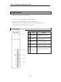
Set value
Output condition
0
Output of the medium value of setting range.
1
The previous value remains.
2
Output of the maximum value of setting range.
3
Output of the minimum value of setting range.
Excess range
Set value condition remains in the former range before exceeded
6 -4
Chapter 6. BUFFER MEMORY CONFIGURATION AND FUNCTIONS
6.2.5
SET Data Specification (G3F-DA4V/G3F-DA4I : address 34, G4F-DA1A: address 6)
1) With each channel Bit turning On(1) on SET data address, the G3F-DA4V / G3F-DA4I which a user has
set are executed for the D/A conversion to the data of address 0,1,18~33, G4F-DA1A which a user has
set is executed for the D/A conversion to the data of address 0,1,4,5.
2) Without each channel Bit turning On(1) on SET data address, the D/A module which a user has set isn't
executed for D/A conversion but the module is executed for D/A conversion to the previous set data.
3) SET data specification is as follows.
(1) G3F-DA4V / G3F-DA4I
(2) G4F-DA1A
6.2.6
Channel Operation Data Area (G3F-DA4V/G3F-DA4I :address 35, G4F-DA1A :address 7)
The operation data of each channel is stored to this area
(1) G3F-DA4V / G3F-DA4I
(2) G4F-DA1A
6 -5
Chapter 7. SPECIAL MODULE COMMAND(BUFFER MEMORY READ/ WRITE)
Chapter 7. SPECIAL MODULE COMMAND(BUFFER MEMORY READ/WRITE)
D/A conversion module occupies 16 I/O points.
7.1 LOCAL COMMAND
7.1.1
Buffer Memory Read -GET, GETP Command
Symbol
Descriptions
Device used
N1
Slot number assigned to special module
Integer
N2
Head address of buffer memory of special module which stores
data to read
Integer
D
Head address of device which stores data to read.
M, P, K, L, T, C, D, #D
N3
Number of words of data to read
Integer
< Distinction of GET and GETP>
GET: Continuously executes read while the read signal is on.
GETP: Execute read by switching on the read signal.
ex1) D/A conversion module is mounted on the slot 3 of base, and data from the buffer memory address 35 is read to the
CPU module D35.
7 -1
Chapter 7. SPECIAL MODULE COMMAND(BUFFER MEMORY READ/ WRITE)
7.1.2
Buffer Memory Write - PUT, PUTP Command
Symbol
Descriptions
Device used
n1
Slot number assigned to special module
Integer
n2
Head address of buffer memory of special module which stores
data to write.
Integer
D
Head address of device which stores data to write.
M, P, K, L, T, C, D, #D
n3
Number of words of data to write
Integer
<Distinction of PUT and PUTP>
PUT : Continuously executes write while the write signal is on.
PUTP : Execute write by switching on the write signal.
ex1) D/A conversion module is mounted on the slot 6 of base, and data from the CPU module D2 and D3 is written to the buffer
memory address 2, and 3.
7 -2
Chapter 7. SPECIAL MODULE COMMAND(BUFFER MEMORY READ/ WRITE)
7.2 REMOTE COMMAND
7.2.1
Buffer Memory Read- RGET
<Format>
RGET command
execution condition
[ RGET
Symbol
SI
St
D
S
n
SS]
D
Descriptions
Upper(AB) : the code value of D/A conversion
module
G3F-DA4I:01h, G3F-DA4V : 02h
G4F-DA1A : 81h
Lower(CD) : the slot number of communication
module of the master station(FUEA).
setting range: 0 to 7
Upper(EF) : Slot number of D/A conversion
module of remote station.
setting range: 0 to 31
Lower(GH) : Address number communication
module of remote station(RBEA).
setting range :0 to 63
Head address of device which stores data to read.
S
Head address of special module which stores data to read.
n
Number of words of data to read
Sl
St
SS
Device used
Integer
Integer
M, P, K, L, T, C, D, #D
Integer
Integer, D
condition data display space of link
M, P, K, L, T, C, D, #D
REMARK
To read buffer memory data of D/A conversion module with RGET command, configure the program so
that execution condition of 0 will be changed into 1 on rising edge.
Otherwise, buffer memory data of D/A conversion module won't be read
GM3- K7P- G3I- G3I- G3Q- G3Q- G3LPA2A 30AS D24A D22A TR4A TR2A FUEA
GM3- G3L- G3I- G3F- G3FPA2A RBEA D24A DA4V PA2A
[Buffer memory read]
1) Read buffer memory address 35(1 word) which the channel operation data of D/A conversion module is
stored.
2) Store read data to the next D300
3) Store the data of communication condition to D1.
[Program]
7 -3
Chapter 7. SPECIAL MODULE COMMAND(BUFFER MEMORY READ/ WRITE)
7.2.2
Buffer Memory Write –RPUT
<Format>
RPUT command
execution condition
[ RPUT
Symbol
Sl
St
SI
St
S
D
n
SS]
Descriptions
Upper(AB) : the code value of D/A conversion
module
G3F-DA4I : 01h, G3F-DA4V :02h
G4F-DA1A : 81h
Lower(CD) : the slot number of communication
module of the master station(FUEA).
Setting range: 0 to 7
Upper(EF): Slot number of D/A conversion module
of remote station.
Setting range: 0 to 31
Lower(GH):Address number of communication
module of remote station(RBEA).
setting range :0 to 63
Device used
Integer
Integer
S
Head address of special module which stores data to write.
D
Head address of device which stores data to write.
n
Number of words of data to write.
Integer, D
Ss
Condition data display space of link
M, P, K, L, T, C, D, #D
Integer
M, P, K, L, T, C, D, #D
REMARK
To write on buffer memory data of D/A conversion module with RPUT command, configure the program
so that execution condition of 0 will be changed into 1 on rising edge.
Otherwise buffer memory data of D/A conversion module won't be updated
GM3- K7P- G3I- G3I- G3Q- G3Q- G3LPA2A 30AS D22A D22A RY2A RY4A FUEA
GM3- G3L- G3I- G3F- G3FPA2A RBEA D24A DA4V PA2A
[Buffer memory write]
1) Write data on D100 to D134(35words) of the CPU module device
2) onto buffer memory address 0 to 34 of D/A conversion module
3) and store the data of communication to D0.
[Program]
7 -4
Chapter 8. MK PROGRAMMING
Chapter 8.
MK PROGRAMMING
8.1 BASIC PROGRAMMING
- This shows the method of operation condition setting for internal memory on the D/A conversion module.
- The D/A conversion module is mounted on the slot 2.
- D/A conversion module occupies 16 I/O points.
8.1.1
G3F-DA4V / G3F-DA4I
Buffer
Channel 0 to 3 : mediu m value is output
Channel 12 to 15 : minimum value is output
Each time to write input data, every channel
is changed to new set data specification
Input data stored on D0 to D15 by the P0 is
written to convert into D/A conversion
Device
to store
8 -1
Chapter 8. MK PROGRAMMING
8.1.2 G4F - DA1A
Input data stored on D1 and D2 by the P0 is
written to convert into D/A conversion
8 -2
Chapter 8. MK PROGRAMMING
8.2 Application Programming
8.2.1 Programming for Controlling Inverter Speed with 5-step Analog Output Voltage
1) System Configuration
GM3PA2A
Initial
K7P30AS
G3ID22A
G3FDA4V
K7SPA2A
(P0000)
(P0001)
(P0002)
(P0003)
(P0004)
(P0005)
2) Initial Settings
(1) Enabled channel : channel 0
(2) Data input type specification :channel 0(-192~16191)
(3) Output condition of D/A conversion module when the CPU is stopping : minimum value output of the range.
(4) Offset : 0 V Gain :5 V
3) Descriptions of the Program
(1) P0000 turning On leads to the initial setting of D/A conversion
(2) P0001 turning On leads to output of "0"(0 V) on channel 0.
(3) P0002 turning On leads to output of "4000"(2.5 V) on channel 0
(4) P0003 turning On leads to output of "8000"(5 V) on channel 0.
(5) P0004 turning On leads to output of "12000"(7.5 V) on channel 0.
(6) P0005 turning On leads to output of "16000"(10 V) on channel 0.
8 -3
Chapter 8. MK PROGRAMMING
4) Program
Specifying the channel 0 as
enabled channel.
initial setting command
Specifying the input data type to
–192 ~ 16191 for the channel 0
While the CPU is stopping, the
output of channel 0 is retained as
the medium valueof the range.
Specifying the SET data for
channel 0.
Setting M0 after initial setting has
been completed.
P0001 turning ON leads to output
of 0 V.
P0002 turning ON leads to output
of 2.5V.
P0003 turning ON leads to output
of 5 V.
P0004 turning ON leads to output
of 7.5 V.
P0005 turning ON leads to output
of 10 V.
8 -4
Chapter 8. MK PROGRAMMING
8.2.2
Programming for Displaying D/A Conversions which is Set by Digital Switch
1) System Configuration
GM3PA2A
K7P30AS
G3ID24A
G3ID22A
G3FDA4V
GM3PA2A
(P0020)
(P0021)
(P0000 ~ P0013)
(P0022)
(P0023)
2) Initial Settings
(1) Enabled channel : channel 0, 1
(2) Data input type specification : channel:0(-8192~8191), channel 1(-192~16191)
(3) Output condition of D/A conversion module when the CPU is stopping : medium value output of the range.
3) Descriptions of the Program
(1) P0020 turning On leads to the initial setting of D/A conversion
(2) P0021 turning On leads to output of the values by digital switch on channel 0 of D/A module.
(3) P0022 turning On leads to output on channel 1.
(4) P0023 turning On leads to initialization of digital input value to "0" on channel 0 and channel 1.
8 -5
Chapter 8. MK PROGRAMMING
4) Program
Specifying the channels 0 and 1 as
enabled channels
initial setting command
Specifying the input data type to
–192 ~ 16191
While the CPU is stopping, the
outputs of channels 0 and 1
are retained as the medium value
of the range.
Specifying the SET data for
channels 0 and 1
Setting M0 after initial setting has
been completed.
Storing the value input by the BCD
digital switch to D10.
If D10 is equal to or less than
16000, M1 is set to ON.
Output is specified to channel 0
P21 turning On makes the data of
D10 output to the channel 0 of the
D/A conversion module.
Output is specified to channel 1
P22 turning On makes the data of
D10 output to the channel 1 of the
D/A conversion module.
When a initialization command is
given, output commands for
channels 0 and 1 are disabled.
initialization
command
P23 turning On makes digital input
values to the channels 0 and 1 of
the D/A conversion module to be 0.
8 -6
Chapter 8. MK PROGRAMMING
8.2.3
Programming for Mounting D/A Conversion Module on Remote I/O Station
This is programming for output D/A conversion value set by digital switch.
1) System Configuration
GM3PA2A
K7P30AS
G3FFUEA
G3ID24A
G3ID22A
(P0030)
digital switch
Remote
Station No.”1”
(P0010 ~ P0023)
GM3PA2A
G3LRBEA
G3FDA4V
GM3PA2A
2) Initial Settings
(1) Enabled channel : channel 0,
(2) Conversion data input type specification : channel 0(-192~16191)
(3) Output condition of D/A conversion module when the CPU is stopping : minimum value output of the range.
3) Descriptions of the Program
(1) P0030 turning On leads to displaying D/A conversion value set by digital switch on channel 0.
8 -7
Chapter 8. MK PROGRAMMING
4) Program
Specifying the channels 0 as
enabled channel
Code value of D/A
conversion module
Specifying the input data type to–192 ~ 16191
Head address of
commun icati
buffer memory
Conversion module loaded where data is written on
Slot No. of the D/A
on remo te station
Slot No. of the local
communication module
Remote
station
No.
Head address Numbers of words
of the device to write data
where write
data is stored
Writing the values stored
in D0 and D1 to buffer
memories of addresses 0
and 1.
M0 is set to ON when no error occurs during communication.
Specifying the SET data for
channel 0
Writing the values stored
in D34 to buffer memory
of address 34
M10 is set to ON when no error occurs during communication.
Storing the BCD digital value
to D100
If the BCD digital switch value is equal to or less than 16000
M200 is turned ON for 1 scan.
Writing the values stored
in D100 to buffer memory
of address 2
Reading information on
run channels
8 -8
Chapter 9. TROUBLESHOOTING
Chapter 9.
TROUBLESHOOTING
This section shows the descriptions of the error code and troubleshooting during use of the D/A conversion
module.
9.1 Error Code Indicated by RUN LED Flickering
This part shows the descriptions of the error code on flickering of RUN LED of D/A conversion module.
RUN LED
Descriptions
Flickers(per 0.1sec)
WDT error
System error
Buffer memory error
Offset/Gain setting error
Flickers(per 0.2sec)
Remark
9.2 Troubleshooting Procedure
9.2.1
RUN LED Flickering
RUN LED flickering
RUN LED flickering(per 0.1 sec) ?
Change test mode condition to normal mode condition
Yes
Yes
No
G3F-DA4V/ G3F-DA4I: No connection of terminal 1 and 2
No
G4F-DA1A: No connection of terminal 1 and 3
RUN LED flickering(per 0.2sec)?
Correct Offset/ Gain setting value.
Yes
Yes
No
No
See Section 9.2.7
9 -1
Chapter 9. TROUBLESHOOTING
9.2.2
RUN LED Off
RUN LED off
Offset/Set/Gain switch is located on Set position of test mode?
Change test mode condition to normal mode condition
Yes
Yes
No
No
Install the D/A conversion module on the base?
Install the D/A conversion module on the base correctly
No
Yes
Yes
No
Capacity sufficient for the power supply module on the base?
Calculate current consumption and replace the
No
Yes
Yes
power supply module
No
If D/A conversion module on which the error has occurred
is substituted for new one, normal operation?
See Section 9.2.7
Yes
Yes
No
No
Fault of other module, not the D/A conversion module.
For more information, see the CPU module User's Manual.
9 -2
Chapter 9. TROUBLESHOOTING
9.2.3
Sudden D/A Output Value Change
Sudden D/A output value change
D/A conversion module and external device are
connected correctly
For the correct wiring, see Section 3.2
No
Yes
Yes
No
External power supply (±15 VDC) is supplied
Make external power supply (±15 VDC) be supplied.
No
Yes
Yes
No
External power supply (±15 VDC) is supplied
sufficiently
Make external power supply (±15 VDC) be supplied
No
Yes
Yes
sufficiently
No
See Section 3.2
Not to be under the effect of noise from wiring
with external device
Sudden D/A output value change
See Section 9.2.7
9 -3
Chapter 9. TROUBLESHOOTING
9.2.4
Digital and Analog Value Mismatch
Digital and analog value mismatch
D/A conversion module and external device are connected correctly.
For the correct wiring, see Section 3.2
No
Yes
Yes
No
Specify channel enable correctly
Specify channel selection correctly
No
Yes
Yes
No
Specify data type in correct
Specify data type in correct
No
Yes
Yes
No
Offset/gain has been set in correct
Set offset/gain setting in correct
No
Yes
Yes
No
See Section 9.2.7
9 -4
Chapter 9. TROUBLESHOOTING
9.2.5
D/A Output Value Always deviates from Specified Value.
Constant D/A output value deviation from reference
value
External power supply is supplied in correct
Supply external power supply in correct
No
Yes
Yes
No
Offset/ gain is adjusted correctly
Adjust offset/gain setting correctly
No
Yes
Yes
No
The D/A conversion module and external device
are connected correctly
For the correct wiring, See Section 3.2
No
Yes
Yes
No
D/A output value is exceeding the range
Set D/A input value according to the range
No
Yes
Yes
No
See Section 9.2.7
9 -5
Chapter 9. TROUBLESHOOTING
9.2.6
Analog Output Value According to the D/A Input Value isn't Changed
Analog output value according to the D/A input
value isn't changed
Available channel enable is specified correctly
Correct available channel enabled
No
Yes
Yes
No
Offset/gain value is set correctly
Set offset/ gain value correctly
No
Yes
Yes
No
Connected with external device correctly
Connect with external device correctly
No
Yes
Yes
No
See Section 9.2.7
9.2.7
D/A conversion module hardware fault
D/A conversion module hardware fault.
Please contact the service station with fault details
9 -6
Chapter 10. G3F-PA1A/ G3F-PA2A POWER SUPPLY MODULE
Chapter 10.
G3F-PA1A/G3F-PA2A POWER SUPPLY MODULE
G3F -PA1A/G3F -PA2A power supply modules are shown in this section.
10.1 Performance Specifications
Performance specification is like the table10.1.
Specifications
Items
G3F-PA1A
Baselocation
G3F-PA2A
Onslotformounting input/output module
Input power supply voltage
110 VAC (85~132 VAC)
220 VAC ( 170~264 VAC)
Input power supply current
1.3A (110 VAC)
0.65 A(220 VAC)
Input frequency
47~63 H z
current
30 Ap-p or less
Ratedoutput
current
*1 Overcurrent
protection
15 VDC
2.0 A
-15 VDC
1.2 A
15 VDC
2.2~ 3.5 A
-15 VDC
1.3~2.5 A
Efficiency
65% or more
Power supply display
LED
Relevance power cable
0.75~2 ㎟
Relevance tighten torque
12KgㆍC m
Weight
820 g
Rated fuse
250 VAC,3 A
[Table 10.1] Performance specifications
REMARK
*1 Overcurrent protection
1)When Currentm ore than reference is flow ing on the15 VDC/-15 VDC circuit, overcurrent
protection device allows the circuit and/or output value to be stopped
2)Once this device is operated, restart the circuit after getting rid of the causes such as deficiency of
current and short circuit
10 - 1
Chapter 10. G3F-PA1A/ G3F-PA2A POWER SUPPLY MODULE
10.2 Notes on Handling
From unpacking to installation, be sure to check the following:
1) Do not drop it off, and make sure that excessive shock should not be applied.
2) Do not dismount the printed circuit board(PC B )from the case. It can cause malfunctions.
3) During wiring, be sure to check any foreign matter like wire scraps should not enter into the upper side of the
PLC, and in the event that foreign matter entered into it, always eliminate it.
10.3 Names of Parts
NO
Name
①
LED display for
power supply
②
Power fuse
③
Descriptions
Indicates LED display for displaying
power input
Indicates 3 A fuse fixed for AC input
power with a fuse holder.
PA1A Connect 110 VAC intotheterm inal
Power input terminal
PA2A Connect 220 VAC intotheterminal.
④
FG
⑤
Terminal of +15 V,
0 V,-15 V
10 - 2
Indicates a term inal grounded with
shielding pattern of PCB panel
Indicates terminals for supplying±15
VDC.
Chapter 10. G3F-PA1A/ G3F-PA2A POWER SUPPLY MODULE
10.4 Dimensions
10 - 3
Chapter 11. DIMENSIONS
Chapter 11. DIMENSIONS
11.1
G3F-DA4V / G3F-DA4I Dimensions
11 - 1
Chapter 11. DIMENSIONS
11.2 G4F-DA1A Dimensions
11 - 2