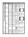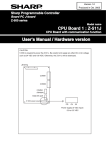
1
Version 1.0
Produced in Oct. 2005
R
Sharp Programmable Controller
Board PC J-board
Z-300 series
Model name
Serial Interface board : Z- 354J
User's Manual
Thank you for purchasing our J-board: Z-300 series programmable controller. This manual describes
specifications and discusses the use of the serial interface board.
See the "J-board Z-300 series Z-311J/312J, Z-321J: User's Manual: Hardware Version" for installation
methods and basic application of this board.
Note
- Should you have any questions or inquires, please feel free to contact one of our dealers, or our
service department.
- Copying the whole or part of this manual is prohibited.
- The contents of this manual may be revised without notice.
Table of contents
Safety Precautions
Chapter 1: Outline ...................................................................................................... 1-1
Chapter 2: Handling Precautions ............................................................................. 2-1
Chapter 3: System Configuration ............................................................................. 3-1
Chapter 4: Name and Function of Each Part ........................................................... 4-1
Chapter 5: Installation/Wiring Method ..................................................................... 5-1
5-1 Installation method .............................................................................................................................
5-2 Wiring method ....................................................................................................................................
[1] Pin assignment of CN2 external communication connector .....................................................
[2] Connection example .................................................................................................................
5-1
5-2
5-2
5-3
Chapter 6: How to Use ............................................................................................... 6-1
[1] Allocation of IO relays ............................................................................................................... 6-2
[2] Settings of parameter area, control relay area .......................................................................... 6-3
[3] Parameter setting ...................................................................................................................... 6-4
[4] Control relay .......................................................................................................................... 6-13
[5] Sending data ........................................................................................................................... 6-16
[6] Recieving data ........................................................................................................................ 6-17
Chapter 7: Program Example ................................................................................... 7-1
Chapter 8: Error and Treatment ............................................................................... 8-1
Chapter 9: Specifications ......................................................................................... 9-1
Appendix ................................................................................................................ App-1
Appendix 1. Parameter address and parameter name .............................................................. App-1
Appendix 2. Address and name of control relay ........................................................................ App-2
Safety Precautions
Read this user's manual and attached documents carefully before installation, operation, maintenance and
checking in order to use this board correctly. Understand all of this board's knowledge, safety information,
and cautions before starting to use. In this user's manual, safety precautions are ranked into "Danger" and
"Caution" as follows.
Danger
: Wrong handling may possibly lead to death or heavy injury.
Caution
: Wrong handling may possibly lead to medium or light injury or loss on properties.
Caution , a serious result may be experienced depending on the
Even in the case of
circumstances. Anyway, important points are mentioned. Be sure to observe them strictly.
The picture signs of prohibit and compel are explained below.
: It means a don’t. For example, prohibition of disassembly is indicated as (
: It means a must. For example, obligation of grounding is indicated as (
).
).
1) Installation
Caution
• Use in the environments specified in the catalog and user's manual.
Electric shock, fire or malfunction may be caused when used in the environments of high
temperature, high humidity, dusty or corrosive atmosphere, vibration or impact.
• Install according to the instruction manual and user's manual.
Wrong installation may cause a drop, trouble or malfunction.
• Never admit wire chips or foreign matters.
Or fire, trouble or malfunction may be caused.
2) Wiring
Compel
• Be sure to ground.
Unless grounded, electric shock or malfunction may be caused.
Caution
• Wiring should be done by a qualified electrician.
Wrong wiring may lead to fire, trouble or electric shock.
3) Use
Danger
• Never touch the terminals while electric power is charged.
Otherwise, you may have an electric shock.
• Assemble an emergency stop circuit and interlock circuit outside of the J-board and integrate
the J-board's halt output. Otherwise a machine breakdown or accident may be caused by the
trouble of the programmable controller.
Caution
• Manipulation for program change, forced output, RUN or STOP during operation should be
done with particular care by confirming safety. Mis-operation may lead to a machine trouble or
accident.
• Follow the power input order specified. Otherwise, the J-board malfunctions and damages
machines or cause an accident.
4) Maintenance
Prohibit
• Don’t disassemble or modify.
Or fire, trouble or malfunction may be caused.
Caution
• Make sure to turn OFF the power before removing / installing the board, installing the
connectors, or changing the switch settings.
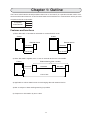
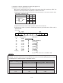
Chapter 1: Outline
The Z-354J serial interface board (hereafter referred to as "the board") is a special I/O board used to communicate with external devices. It has RS-232C/422A serial interfaces for communication with a personal
computer and a bar code reader.
Compatible
motherboards
Z-311J
Z-312J
Z-313J
Features and functions
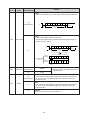
1) Either RS-232C or RS-422A is selectable as communication mode.
Z-354J
Z-354J
External device
External device
RS-232C
RS-422A
15 m or less
1 km or less
2) When RS-422A is applied, max. 15 sets of external devices are connectable.
Z-354J
External device (max. 15 sets)
RS-422A
RS-422A
RS-422A
1 km or less
3) Applicable to various data formats for exchanging data with external device.
4) Max. 512 bytes of data sending/receiving is possible.
5) Outputs error information by error codes.
1-1
Chapter 2: Handling Precautions
(1) Precautions for installation
Never install the board in the following locations.
· Where proximate to any heat generating object.
· Where temperature rapidly changes and gives dew condensation.
· Where there is flammable gas.
· Where it directly receives vibration or shocks.
· Where exposed to dust, iron powder, or salty atmosphere.
(In conditions where the printed circuit boards may be directly affected by these causes, make sure to
provide an appropriate external case to cover the J-board.)
· Where it is proximate to high voltage equipment, driving power tools, large open/close surge generating devices, and their wirings.
(2) Precautions at use
· In order to prevent personal injury or damage to equipment, construct an external emergency stop
circuit and connect it to the halt output on the J-board.
· As J-board is board structure and it’s electronic parts are exposed, be careful when handling.
1) Before you touch the board directly, be sure to eliminate static electricity in your body.
2) Do not touch directly with dirty hands such as stacked oil etc.
3) Do not put the board alone directly on conductive objects such as metallic boards.
(Once the J-board is installed on a motherboard, if it contacts a conductive object the battery on
the motherboard may be short circuited and the back up memory may be damaged.)
4) Be careful not to apply excessive force to each switch, connector, terminal block of the J-board.
· Make sure to turn OFF the power before connecting the board, installing connector, changing a
switch setting.
(3) Precautions for wiring
Do not run the communication lines parallel to or near to power lines or high voltage lines. Do not
arrange wiring so that sources of electrical noise (driver lines, high voltage lines, or I/O lines) come
close to the PC board on the J-board.
2-1
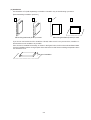
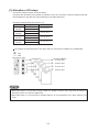
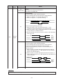
(4) Installation
Use bracket A or B (sold separately) to install the J-board in any of the following 4 positions.
[Recommending installation positions]
1
2
3
When fixing bracket A (Z-341J) is used
4
When fixing bracket B (Z-342J) is used
If you do not use bracket A or B to install the J-board, make sure it is very secure. Also, install the Jboard with as much ventilation as possible.
If the J-board is installed horizontally, as shown in the figure below, it will not be well ventilated. Make
sure the installation allows enough space above the board so that the surrounding temperature does
not rise above 55˚C.
Not good ventilation
2-2
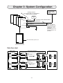
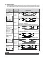
Chapter 3: System Configuration
Personal computer,
NC liquid crystal
terminal or similar
devices.
Stacking structure
(Up to 4 I/O boards or communication
boards can be connected)
Support
tool
CPU
PG port
CN (15P)
CN (9P)
Terminal block
(7P)
Proprietary cable (JW-22KC/24KC)
Upstream communication port
(RS-232C) 1 : 1
Upstream communication port
(RS-422A) N : 1
Either RS-232C or
422A standards can
be used for communication with a host
controller.
(Simultaneous use of
both standards is not
possible.)
24 VDC in
FG
Bar code reader, printer, etc.
Z-354J
Serial interface board
Data flow chart
CPU board
This board (Z-354J)
Data register
Common RAM
Sending buffer
・Add sending header/terminator
Data
Sending data
・Data
3-1
Data
Sending
terminator
Data
Receiving
terminator
Receiving buffer
Receiving data
Receiving
data
Data
Sending
header
Sending
data
Receiving
header
Data
Data
Sending
terminator
Data
transfer
・Delete receiving header
/terminator
・Data
(Non-conversion,
ASCII → BIN conversion)
Sending
header
(Non-conversion,
BIN → ASCII conversion)
Receiving
terminator
Max.
512
bytes
Data
transfer
Receiving
header
Max.
512
bytes
External device
Chapter 4: Name and Function of Each Part
SW2
2
Z-354J
1
ON
Bus connector CN1
(connection to another board)
TX
RX
RS
CS
Green
EA
EB
(CK)
FT
Red
SW1 (RACK No.)
3
2
1
ON
LED
SW3
9
6 78
SW3
F012
CD
AB E
345
Module No. switch SW4
SW4
456
23
External communication connector CN2
(D-sub 25-pin female, Details are on page 5-2)
901
78
Termination resistance switch SW5
ON
Self diagnosis switch
SW6
ON
- Setting switches
Switch name
Switch type
1
SW1
2
1
2
Setting details
OFF
Dip switch (3 poles)
3
SW2
Setting
when
delivered
OFF
Specify a rack no.
Factory setting: Rack address 0
OFF
Dip switch (2 poles)
ON
ON
Use it with the factory setting (ON).
SW3
Rotary switch (0 to F)
0
Use it with the factory setting (0).
SW4 (Module No.
switch)
Rotary switch (0 to 9)
0
Specify a parameter area and a control relay
area.
SW5 (Termination
resistance switch)
Slide switch (1 pole)
ON
Only need to set this switch when connecting
by selecting the RS-422A protocol.
("ON" enables a termination resistance, and
"OFF" removes the termination resistance)
For details, see the next page.
SW6 (Self
diagnosis switch)
Slide switch (1 pole)
OFF
The setting for this switch must not be
changed. Keep the factory settings.
(ON enables the self diagnosis)
4-1
- LED display
Indication
LED
Display details
color
TX
Green
Is ON while sending date (J-board -> external device).
RX
Green
Is ON while receiving date (J-board <- external device).
Is ON when the J-board is requesting an external device to send data (the JRS
Green
board is ready to receive).
Is ON when the J-board can send data to an external device (waiting for an
CS
Green
external device that is ready to receive).
EA
Red
Goes ON when any of the parameters or control relay settings are out of range.
EB
Red
Goes ON when a communication error occurs, such as parity error, or time out.
(CK)
Red
On during self diagnosis (goes OFF in normal use).
FT
Red
Goes ON when a hardware error occurs on the J-board.
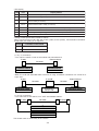
- Setting of SW5 (termination resistance switch)
When communication mode is RS-422 (2-wire system, 4-wire system), set termination resistance.
At RS-232C, this setting is not required.
Setting
Condition of the board
ON
Insert termination resistance
OFF
Do not insert termination resistance
("1" by "1" connection)
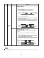
• Turn "ON" the switch on both of the module and external device.
External device
Z-354J
RS-422A
Termination
resistance switch
ON
Termination
resistance switch
ON
• When Z-101HE (RS-232C/RS-422A converter) is using, termination resistance of Z-101HE is always "ON."
Z-354J
Z-101HE
RS-422A
External device
RS-232C
Termination
resistance switch
ON
Termination
resistance switch
ON or OFF is OK
Termination
resistance is
always "ON"
("1" by "N" connection)
• Turn "ON" both of end stations, turn "OFF" intermediate stations.
RS-422A
RS-422A
RS-422A
Termination resistance switch
OFF
Termination resistance switch
ON
Thisº board need not necessarily be end station.
4-2
Chapter 5: Installation/Wiring Method
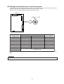
5-1. Installation method
Shown below are the PC board dimensions and assembled dimensions of the Z-354J.
- PC board dimensions
100
5
*5
[Unit: mm]
Standoff hole
4-φ4
170
180
5
Brackets are not included in the dimensions on the left.
117.5
- Assembly dimensions (when 4 sets of the Z-354J are stacked)
[Unit: mm]
25.0
CPU board *
21.6
126.4
21.6
Serial interface board Z-354J
21.6
21.6
15.0
In case of fixing bracket A
* CPU board should be installed on the top.
For the details about assembling and installing the board, see the "J-board Z-311J/312J, User's
Manual, Hardware Version."
5-1
5-2. Wiring method
This board can be connected to either an RS-232C or RS-422A (2-wire system, 4-wire system) device through external communication connector CN2.
[1] Pin assignment of CN2 external communication connector
Internal circuit diagram of this board
Communication connector
(D-sub25P)
RS-232C
FG
1
SD
2
RD
3
RS
4
CS
5
6
SG
7
8
9
SD(+) 10
RS-422
SD(-) 11
RD(+) 12
RD(-) 13
Std.
RS-232C
––
RS-422A
––
FG
14
SD
15
RD
16
RS
17
CS
18
19
SG
20
SD
1
RS-232C
2
3
RS-422
4
RS
5
CS
7
2-wire system
21
22
23
24
25
SD(+)
SD(-)
RD(+)
RD(-)
RD
4-wire system
10,22
11,23
12,24
13,25
Signal direction
Pin No.
Signal name
1
FG
Frame ground
2
SD
Sending data
Z-354J -> External device
3
RD
Receiving data
Z-354J <- External device
4
RS
Request to send
Z-354J -> External device
5
CS
Ready to send
Z-354J <- External device
6
––
Not used
––
7
SG
Signal ground
––
8, 9
––
Not used
––
10,22
SD (+)
11,23
SD (–)
12,24
RD (+)
13,25
RD (–)
14 to 21
––
Function
Sending signal
Receiving signal
Not used
5-2
––
Z-354J -> External device
Z-354J <- External device
––
[2] Connection example
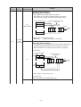
(1) RS-232C (In case of control signal: absent, XON/XOFF manual, or XON/XOFF automatic)
Z-354J
Pin No. Signal name
Shield cable
External device
Signal name
1
FG
FG
2
SD
SD
3
RD
RD
7
SG
SG
15 m or less
RS and CS of external device might be shorted in accordance with specification (available operation
when both RS and CS are "ON") of its external device.
Some external device cannot communicate unless DCD (carrier detection) is "ON."
In this case, latch DCD terminal signal at the external device side or loop back "ON" voltage signal.
(2) RS-232C (In case of control signal: RS/CS manual, or RS/CS automatic)
Z-354J
Pin No. Signal name
Shield cable
External device
Signal name
1
FG
FG
2
SD
SD
3
RD
RD
4
RS
RS
5
CS
CS
7
SG
SG
15 m or less
(3) RS-422A (4-wire system)
"1" by "N" connection is available. (Max. 15 sets for N)
Z-354J
Pin No. Signal name
1
10
11
12
13
22
23
24
25
External device 1
External device 2
Shield cable
Shield cable
Shield cable
External
device N
Signal name
Signal name
Signal name
FG
SD (+)
FG
SD (+)
FG
SD (+)
FG
SD (+)
SD (—)
RD (+)
SD (—)
RD (+)
SD (—)
RD (+)
SD (—)
RD (+)
RD (—)
RD (—)
RD (—)
RD (—)
1 km or less
This board needs not necessarily to be end station.
5-3
(4) RS-422A (2-wire system)
"1" by "N" connection is available. (Max. 15 sets for N)
Z-354J
Pin No. Signal name
External device 1
External device 2
Shield cable
Shield cable
Shield cable
Signal name
Signal name
External
device N
Signal name
1
FG
FG
FG
FG
10
SD (+)
SD (—)
SD (+)
SD (—)
SD (+)
SD (—)
SD (+)
SD (—)
11
1 km or less
This board is not necessary be an end station.
(5) Using Z-101HE (RS-232C/RS-422A converter)
1) 4-wire system
Shield cable
Z-354J
Z-101HE
RS-422A
Pin No. Signal name
Terminal name Pin No.
(4-wire system)
1
FG
Grounding
1
10
SD (+)
TD (+)
2
11
SD (—)
TD (—)
3
12
RD (+)
RD (+)
7
13
RD (—)
RD (—)
1 km or less
Shield cable
RS-232C
External
device
Signal name
FG
SD
RD
SG
15 m or less
2) 2-wire system automatic
Z-354J
Pin No. Signal name
1
Shield cable
RS-422A
(2-wire system)
Z-101HE
Terminal name Pin No.
Shield cable
RS-232C
External
device
Signal name
Grounding
RD (+)
1
FG
10
FG
SD (+)
2
SD
11
SD (—)
RD (—)
3
RD
7
SG
1 km or less
15 m or less
• RS and CS of external device might be shorted in accordance with specification (available operation when both RS and CS are "ON") of its external device.
Some external device cannot communicate unless DCD (carrier detection) is "ON."
In this case, latch DCD terminal signal at the external device side or loop back "ON" voltage signal.
• When Z-101HE automatic mode is applied, set transfer rate 2400 bits/s or up.
Notes
* Be sure to use the following shielded twisted pair cables.
Manufacturer
RS-232C, RS-422A (4-wire system)
HITACHI CABLE LTD
CO -SPEV -SB0.5
RS-422A (2-wire system)
S -IREV -SW2*0.5
* Wire the communication cable as far apart as possible from power lines or high voltage lines, so as not
to run close or parallel to them.
5-4
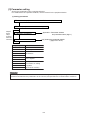
Chapter 6: How to Use
Standard operation flow is shown below. Refer to this for use.
Reference item (Pages to refer )
1. Turn OFF power supply to J -board.
(6-2)
2. Set termination switch SW1.
3. Set parameter area and control relay
area by module No. switch.
Setting of parameter area, control
relay area (6-3)
(4-2)
4. Set termination resistance switch
5. Check the switch settings
SW2-1 = ON, SW2-2 = ON
SW3 = 0
SW6 = OFF
6. Install the board together with a CPU board, etc.
Installation method (5-1)
7. Connect external devices to the board.
Wiring method (5-2 to 4)
8. Turn ON the power supply to the board
9. Set parameter.
Parameter setting (6-4 to 12)
10. Create program of J-board.
Control relay
(6-13 to 15)
Program example (7-1, 2)
11. Enter the J-board in operation
condition using a support tool.
12. Start communication between the
board and the external device.
6-1
[1] Allocation of I/O relays
This board contains 8 bytes, as shown below.
I/O relays are allocated on this board as dummies. They do not function. However, please note that
their assignment may affect I/O relay addresses on another I/O board.
Allocation example when the rack No. is 0.
Allocation
Dummy
(vacant)
I/O relay address Actual address
コ .000
R = 0, S = 0
コ .001
Dummy
(vacant)
Dummy
(vacant)
Dummy
(vacant)
コ .002
コ .003
コ .004
コ .005
コ .006
コ .007
R = 0, S = 1
R = 0, S = 2
R = 0. S = 3
- Turn SW2-1 and SW2-2 ON
An example of the assignment of I/O relays when an I/O board is installed on a motherboard.
ON
OFF
SW1 (Rack No.) SW2
I/O relay address
コ013 to コ037
64 points I/O board
Z-322J
64 points I/O board
Z-322J
コ020 to コ027
This board
Z-354J
コ010 to コ017
This board
Z-354J
コ000 to コ007
CPU board
Z-312J
* When SW1 (rack no.) is set the to same number for multiple J-boards, they may have the same I/O
allocations which can cause a malfunction.
* When SW1 (rack no.) is turned ON on multiple stations, an "I/O verification error: Error code 60" will
occur.
6-2
[2] Settings of parameter area, control relay area
Set parameter area to designate communication mode, transfer rate etc., and control relay area required for data sending/receiving programs using a module No. switch.
Be sure not to set same number with other special I/O module.
Z-354J
Module no. switch
SW4
456
901
78
23
* Parameter area
Module No. switch
Control relay area
setting value
Parameter address Register address of file 1 (byte address)
0
T- 0 (000 to 177)
000000 to 000177
コ0200 to コ0217
1
T- 1 (000 to 177)
000200 to 000377
コ0220 to コ0237
2
T- 2 (000 to 177)
000400 to 000577
コ0240 to コ0257
3
T- 3 (000 to 177)
000600 to 000777
コ0260 to コ0277
4
T- 4 (000 to 177)
001000 to 001177
コ0300 to コ0317
5
T- 5 (000 to 177)
001200 to 001377
コ0320 to コ0337
6
T- 6 (000 to 177)
001400 to 001577
コ0340 to コ0357
7
T- 7 (000 to 177)
001600 to 001777
コ0360 to コ0377
8
Prohibited to set
9
* Depending on a peripheral device used for entering parameters, addresses to enter vary. (=> Next
page)
* Only set the module no. switch when the power to the J-board is OFF. Use a slotted screwdriver.
6-3
[3] Parameter setting
Specify the parameters using a peripheral device.
For details about the operation methods, see the manual for the peripheral device.
(1) Setting procedures
① Connect the peripheral device to the CPU board of the J-board.
② Put the peripheral device in the setting mode.
Repeat
these
steps
as many
times as
necessary.
③ Read the set address.
Appendix 1: Parameter address
and parameter name (App-1)
④ Read the set value
(2) Setting the parameter details
(page 6-5 to 6-12).
Peripheral device
Address to set
JW-2PG
Parameters
JW-10PG
File 1 register
JW-11PG
JW-12PG
Parameters
JW-13PG
ZW-101PG1
File 1 register
Z-100LP2F
JW-40PG
Specify the JW21/22
JW-50PG
parameters for editing
programs
JW-92SP
(Special I/O module)
JW-52SP
* When the power is turned ON or the J-board status changes from "stop" to "operating," the J-board's
motherboard transfers the parameters to the J-board, and specifies the communication conditions.
6-4
(2) Setting the parameter details
The address shown below is parameter address. In case of register address of fiel 1, refer to appendix. 1.
Address Parameter Setting value
Details
T-0 to 7
name
(Hexadecimal)
Execution of parameter transfer
22
- Transfer parameters from CPU board's memory
Parameter
000
(Initial value: 00) to the board
transfer
- Other than 22HEX is treated as prameter transfer
error.
00
Completion of BCC calculation
(Initial value)
Execution of BCC calculation
- At changing parameter, set to 01HEX.
BCC
- When the CPU board's changes from "program
001
calculation
mode" to "date transfer mode" or it turns from
01
OFF to ON, it calculates BCC codes of
parameter setting contents and stores in
parameter address 177.
- When the calculation is completed, set to 00HEX.
RS-232C
00
(Initial value) - Transfer mode is fixed to full-duplex.
002
Communication
mode
01
02
00
(Initial value)
003
Transfer
mode
01
004
Transfer
speed
00
(Initial value)
01
02
03
04
05
RS-422A (4-wire system)
- Either full-duplex or half duplex is selectable as
transfer mode.
RS-422A (2-wire system)
- Transfer mode is fixed to half-duplex.
Full-duplex
- Both sending and receiving data at the same
time is possible.
- In case of RS-422A (2-wire system), it is fixed to
half-duplex so that this setting is invalid.
Half-duplex
- Execute sending and receiving alternately.
- In case of RS-232C, it is fixed to full-duplex so
that this setting is invalid.
19200 bits/s
9600 bits/s
4800 bits/s - Select to match the external
device's specifications
2400 bits/s
1200 bits/s
600 bits/s
6-5
Address Parameter Setting value
T-0 to 7
name
(Hexadecimal)
Details
8 bits
• Data to be subject to JIS code, binary data, special character.
00
(Initial value)
1
D0
D1
D2
Start
bit
005
D3
D4
D5
D6
D7 Parity
0
Parity Stop bit
bit (Ex.: 2 bits)
Data length
(8 bits)
7 bits
• Data to be subject to ASCII code only.
• At communication with an external device the data length of
which is fixed to 7 bits.
Data length
1
D0
D1
D2
D3
D4
D5
D6 Parity
0
Start
bit
01
At data
sending
D7
Parity Stop bit
bit (Ex.: 2 bits)
Data length
(7 bits)
D6
CPU board data
(1 byte)
D5
D4
D3
D2
D1
D0
D3
D2
D1
D0
Neglect
At data
receiving D7
D6
D5
D4
Becomes 0
006
007
Stop bit
00
(Initial value)
2 bits
01
1 bit
• Select to match the external device’s
specifications
00
(Initial value)
Even
• Set and check that length of total amount of bits of data D0 to
D7 (D0 to D6 at 7 bits data length) and "ON" bit of parity bit
becomes even.
01
Odd
• Set and check that length of total amount of bits of data D0 to
D7 (D0 to D6 at 7 bits data length) and "ON" bit of parity bit
becomes odd.
02
Absent
• Don’t set and check above parity bit.
Parity
6-6
Address Parameter Setting value
T-0 to 7
name (Hexadecimal)
00
(Initial value)
Details
Absent
• No check concerning communication.
• RS relay is normally ON.
RS/CS manual
• Communication mode: Valid at RS-232C.
• Control sending data by CS signal from external device.
1. When CS signal is 0, ready for data sending
2. When CS signal is 1, stop data sending.
Sending data
CS signal
01
010
Control
signal
1
3
4
5
6
7
0
1
→External device
←External device
• Control receiving data by RS relay.
1. When RS relay is OFF, RS signal becomes "1" and
requests to stop data sending to an external device.
2. When RS relay is "ON," RS signal becomes "0" and requests
to send data to an external device.
3. Receiving data time over error due to switch "OFF" RS relay
does not occur.
RS relay
ON
OFF
RS signal
0
1
←JW20
→External
device
Receiving data
02
2
1
2
3
4
5
6
←External
device
RS/CS automatic
• Communication mode: Valid at RS-232C
• Control sending data by CS signal from external device.
Contents is the same as RS/CS manual operation.
• Control receiving data by number of vacant data bytes of
receiving buffer.
1. When number of vacant data bytes becomes less than 16
bytes, RS signal turns to "1" and requests to stop sending
data to an external device.
2. When number of vacant data bytes becomes more than 17
bytes, RS signal turns to "0" and requests to send data to an
external device.
Number of vacant
data bytes of
receiving buffer
RS signal
16 bytes
17 bytes
0
1
←External
device
Receiving data
1
2
3
4
* Match setting of control signal at external device side to this board’s settings.
6-7
5
6
→External
device
Address Parameter Setting value
(Hexadecimal)
T-0 to 7
name
Details
XON/XOFF manual
• Transfer mode: Valid at full-duplex.
• Control sending data by XON, XOFF codes from an external
device.
1. Possible data sending by receiving XON [11HEX].
2. Data stops sending by receiving XOFF [13HEX].
Sending data
1
2
3
Receiving data
03
010
X OFF
6
External
→device
External
←device
X ON
ON
OFF
←CPU board
Sending data
X OFF
Receiving data
04
5
• Control receiving data by RS relay.
1. This board automatically sends XOFF [13HEX] by turning RS
relay from "ON" to "OFF," and requests to stop sending
data to an external device.
2. This board automatically sends XON [11HEX] by turning RS
relay from "OFF" to "ON," and requests to send data to an
external device.
3. Receiving data time over error by turning OFF RS relay
does not occurs.
RS relay
Control
signal
4
1
2
3
External
→device
X ON
4
5
6
External
←device
XON/XOFF automatic
• Transfer mode: Valid at full-duplex.
• Control sending data by XON, XOFF codes from external
device.
Contents is as same as XON/XOFF manual operation.
• Control receiving data by number of vacant data bytes of
receiving buffer.
1. When number of vacant data bytes is less than 16 bytes,
this board automatically sends XOFF [13HEX] and requests
to stop sending data to an external device.
2. When number of vacant data bytes is more than 17 bytes,
this board automatically sends XON [11HEX] and requests to
send data to an external device.
Number of vacant
data bytes of
receiving buffer
Sending data
Receiving data
1
2
16 bytes
17 bytes
X OFF
X ON
3
4
* Match setting of control signal at external device side to this board’s settings.
6-8
→External
device
5
6
←External
device
Address Parameter Setting value
T-0 to 7
name (Hexadecimal)
Details
Sending: Non-conversion
Receiving: Non-conversion
• Send CPU board’s data without conversion.
• Send data from an external device without conversion.
• JIS codes, binary data are usable (data length: 8 bits).
Inside of sending/receiving buffer
CPU board data register
of this board
Non-conversion
1st byte
Terminator
"n"th char.
Header
Sending
→
(←) External
device
Top data
"n"th byte
* Max. value of n (2 points) is 512.
* Values in (
) means conditions at receiving.
Transfer
code
conversion
Sending: BIN −> ASCII conversion
Receiving: Non-conversion
• Send data after convert BIN data of CPU board to ASCII form.
(Sending header/terminators are sent without conversion.)
• Receive data from an external device without conversion.
(At sending)
"n"th Upper
byte 4 bits
Lower
4 bits
Top data
* Max. value of n (2 points) is 512.
(At receiving)
Same as receiving of setting value 00HEX.
6-9
Terminator
2nd char.
2nd char.
01
1st char.
CPU board data register
Inside of sending buffer
MSB
LSB
of the module
1st
Upper Lower
byte 4 bits
4 bits BIN→ASCII conversion
Sending data
Header
011
2nd char.
Sending data
(Receiving data)
2nd byte
1st char.
00
(Initial value)
Sending
→
External
device
Address Parameter Setting value
(Hexadecimal)
T-0 to 7
name
Contents
Sending: Non-conversion
Receiving: ASCII −> BIN conversion
• Send CPU board’s data without conversion.
• After converting data from an external device from ASCII to
BIN, take as CPU board’s data.
• Only 0 to 9, A to F are usable as ASCII characters for receiving
data (except receiving header, terminator).
(At sending)
Same as sending of setting value 00HEX. (See previous page)
(At receiving)
"n" th Upper
byte 4 bits
Lower
4 bits
Terminator
2nd char.
2nd char.
Transfer
code
conversion
1st char.
011
Header
02
CPU board data register
Inside receiving buffer
MSB
LSB
of this board
1st Upper Lower
byte 4 bits
4 bits
ASCII→BIN conversion
Receiving data
Receiving
←
External
device
Top data
* Max. value of "n" (2 places) is 512.
* Be sure to set number of receiving characters to even by an
external device.
03
Sending: BIN −> ASCII conversion
Receiving: ASCII -> BIN conversion
• Send data after converting CPU board’s data from BIN to
ASCII. (Send header/terminators without conversion.)
• After converting data from an external device from ASCII to
BIN, take as CPU board’s data.
• Only 0 to 9, A to F are usable as ASCII characters for receiving
data (except receiving header, terminator).
(At sending)
Same as sending of setting value 01HEX. (See previous page)
(At receiving)
Same as receiving setting value 02HEX.
6-10
Address Parameter Setting value
T-0 to 7
name (Hexadecimal)
012
013
Sending
time over
interval
Receiving
time over
interval
Details
00
0 ms
(Initial value)
100 ms
01
200 ms
02
300 ms
03
400 ms
04
500 ms
05
600 ms
06
700 ms
07
800 ms
08
900 ms
09
1000 ms
0A
1100 ms
0B
1200 ms
0C
1300 ms
0D
1400 ms
0E
1500 ms
0F
1600 ms
10
1700 ms
11
1800 ms
12
1900 ms
13
2000 ms
14
Other than above Setting prohibited
00
0 ms
(Initial value)
100 ms
01
200 ms
02
300 ms
03
400 ms
04
500 ms
05
600 ms
06
700 ms
07
800 ms
08
900 ms
09
1000 ms
0A
1100 ms
0B
1200 ms
0C
1300 ms
0D
1400 ms
0E
1500 ms
0F
1600 ms
10
1700 ms
11
1800 ms
12
1900 ms
13
2000 ms
14
Other than above Setting prohibited
6-11
• While sending data, when data stops at
a middle of 1 data frame (see page 616), the timer starts.
• When this board does not send next data
until the sending time over interval, a
sending time out error occurs. When this
board sends next data, it resets the timer
and continues sending.
• Allowance of setting time is 0 to +100
ms.
(Example)
At 00HEX setting: 0 ms to 100 ms
At 01HEX setting: 100 ms to 200 ms
• While the board is receiving data, if the
receiving data stops sending at a middle
of 1 data frame (see page 6-17), the
timer starts counting.
• If the board does not receive the next
data within the receive time out interval,
the receive time out error occurs. If the
board receives the next data within the
specified time interval, the board resets
the timer and continues receiving data.
• Allowance of the specified time is the
same as the sending time out time.
• When the RS/CS manual or XON/XOFF
manual is selected as control signal, and
if the RS relay is OFF, the receiving time
over error does not occur.
Address Parameter Setting value
T-0 to 7
name
(Hexadecimal)
014
015
016
017
Details
• When EXP1 header, EXP1 terminator are set at sending
header/terminator or receiving header/terminator of a control
relay (see page 6-14), any set code in this parameter is valid
as control character.
• When NUL code [00HEX] is set, thereafter set code becomes
invalid so that header can use 1 to 4 characters and terminator can use 1 to 2 characters.
• When NUL code is set at each top address 014, 020, it
becomes header: absent, terminator: absent, conditions.
EXP1
header
(Initial value: 00)
(Setting example)
Address Setting value
020
021
EXP1
terminator
022
023
024
025
EXP2
header
026
027
EXP2
terminator
030
to
176
Not used (Initial value: 00)
177
BCC code
Character
014
3A(H)
015
3F(H)
?
016
00(H)
NUL
017
00(H)
NUL
020
40(H)
@
021
00(H)
NUL
:
Sending/receiving data
Invalid
: ?
Invalid
Header
(2 chars.)
Data
@
Terminator
(1 char.)
• When EXP2 header, EXP2 terminator are set at sending
header/terminator or receiving header/terminator of a control
relay (see page 6-14), any set code in this parameter is valid
(Initial value: 00)
as control character.
• Setting contents is as same as EXP1 header, EXP1 terminator.
––––
––––––––––––––––
• Setting is not required. (Setting by support tool is invalid).
• Store check code of parameter. (This board checks parameter setting values from CPU board using this code.)
6-12
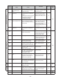
[4] Control relay
Control relays are used for a program to send and receive data.
As for programming, refer to the basic program on "Chapter 7: Program Example."
(1) Control relay contents
Addresses shown below are true when the module No. switch setting is "0." For settings of other
numbers, refer to appendix 2 .
Address
D1
コ0200
D3
D5
D1
D3
コ0201
D4
D5
D7
0202
Name of control relay Contents
- Turns "ON" when data sending to an external device is
TRDY
available.
(Ready sending
- When TRDY relay turns from OFF" to "ON," this board clears
operation)
error codes of control relay and recovers from error condition.
- Turns "ON" when the CPU board requests to send receiving
RREQ
data to this board.
(Request to transfer - While RREQ relay turns from "OFF" to "ON," when this
receiving data)
board has received data, it turns "ON" RACK relay. (It also
clears error codes.)
- Control RS (control signal of RS-232C) from the CPU board,
this signal turns "ON" when requesting to send data to an
RS
external device. (RS signal voltage is +10 V.)
(Request to send)
- Valid when parameter setting of control signal (Page 6-7 and
6-8) is "RS/CS manual" and "XON/XOFF manual."
TREQ
- Turns "ON" when there is no data in sending buffer of this
(Request to transfer
board.
sending data)
RRDY
- Turns "ON" when this board has receiving data, and ready to
(Ready to transfer
transfer to the CPU board.
receiving data)
- Turns "ON" when this board has receiving data while RREQ
RACK
turns from "OFF" to "ON."
- This board transfers receiving data to the CPU board by F-85
(Ready to transfer
instruction while RACK turns from "OFF" to "ON," and turns
receiving data)
"OFF" after completion of transfer.
- Monitors CS (control signal of RS-232C) at the CPU board,
CS
and turns "ON" when an external device is ready to receive
(Ready sending)
data. (CS signal voltage is +3 to +15 V.)
- This board turns "ON" this signal when it ready to operate,
and keeps "ON" condition with both of the below conditions.
URDY
1. Completion of transfer parameter from the CPU board to this
(Available operation
board.
of this board)
2. Mode switch is set to "0."
- This board converts errors which occurred inside to error
codes, and outputs to this address.
- Error code becomes 00HEX (normal operation) at following
Error code
conditions.
(See page 8-1 and 81. When TRDY relay turns from "OFF" to "ON."
2.)
2. J-board starts operation from stopped condition.
- When more than one errors occurs, this board outputs a
priority error code.
6-13
Name of
Setting value
control relay or output value
Details
Receiving
header/
terminator
1HEX
*1
EXP1 header
2HEX
*1
EXP2 header
3HEX
Absent
4HEX
Absent
5HEX
Absent
CR • LF
6HEX
STX
ETX
STX
ETX + BCC (1 byte)
7HEX
*2
Other than above
コ0203
Setting prohibited
Receiving
header
0HEX
D4
to
D7
Sending
header/
terminator
Absent
1HEX
*1
EXP1 header
2HEX
*1
EXP2 header
CR
4HEX
Absent
LF
5HEX
Absent
CR • LF
6HEX
STX
ETX
STX
ETX + BCC (1 byte)
Other than above
コ0204
(Lower)
0000HEX
0001HEX
コ0205
(Upper)
No. of
sending
bytes
to
0200HEX
Other than above
コ0206
(Lower)
コ0207
(Upper)
コ0210
(Lower)
]0211
(Upper)
No. of
transfer
bytes
No. of
receiving
bytes
Top data
End data
Specify these addresses in order to
Absent
determine whether the
EXP1 terminator data sent are intended
for this board or not.
EXP2 terminator
Absent
*2
Data
Receiving
terminator
3HEX
7HEX
Receiving terminator
D0
to
D3
Absent
Specify these addresses in order to
Absent
determine whether the
EXP1 terminator data received are
EXP2 terminator intended for this board
or not.
CR
(Receiving data)
LF
Setting prohibited
(Sending data)
Top data
Sending terminator
0HEX
Receiving
terminator
Receiving header
Receiving
header
Sending header
Address
Data
End data
Variable data • Set number of byte of sending data to
external device.
length
• When number of byte is set to "variable
data length," the module is unable to
1 byte
send while sending terminator is "absent," and automatically calculates
to
number of sending bytes while sending
terminator is "present."
• As for relationship with other settings,
512 bytes
see page 6-16.
Setting
prohibited
0000HEX
0 byte
to
to
0200HEX
512 bytes
0000HEX
to
0 byte
to
0200HEX
512 bytes
Other than
above
Setting
prohibited
6-14
• Setting is not required.
After calculating number of receiving
data bytes from an external device
(except receiving header/terminator),
this board outputs the result to this
address.
• As for relationship with other settings,
see page 6-17.
• Set number of bytes of receiving data
from an external device.
• This setting is valid only when both
receiving header/terminator are "absent."
• As for relationship with other settings,
see page 6-17.
*1 (4 places) – Become parameter set code (see page 6-12.)
*2 (2 places) – How to make a BCC code
BCC check is made based on the calculation of the range from STX onward up to ETX. The
calculations are all performed in bit patterns of ASCII 7-bit codes.
1) Operate XOR of the first character and the second character of the communication data.
Truth table of eXclusive OR
Symbol
A
B
C
A
B
C
0
0
0
1
0
1
0
1
1
1
1
0
2) Operate XOR of the result of that operation and the third character.
3) Determine the result of operation sequentially and, lastly, operate XOR of ETX to take it
as BCC code.
(Example)
1st 2nd
word word
STX
31
32
8th
word
33
34
35
36
37
38
ETX BCC
Calculated area of BCC check
XOR value
ASCII
Binary value
31
110001
32
110010
110001=Result (1)
33
110011
000011=
34
110100
110000=
35
110101
000100=
36
110110
110001=
37
110111
000111=
38
111000
110000=
ETX(03)
000011
001000=
BCC code
001011
* The number of transfer bytes and receiving bytes are values after converting transfer code at data
receiving. Therefore, when this board receives after conversion from ASCII to BIN (page 6-10), number
of data bytes at an external device is 1024 bytes at max.
Number of data bytes at the external device
Number of transfer bytes,
number of receiving bytes Receiving: non-conversion Receiving: ASCII -> BIN conversion
1
1
2
2
2
4
to
to
to
511
511
1022
512
512
1024
6-15
[5] Sending data
Relations between sending header/terminator, number of sending bytes (P6-14) and 1 data frame of
sending data are as follows:
Number of sending byte
Data sending terminator
[Control relay setting value] [Control relay setting value]
Variable data length
[0000HEX]
Absent
0HEX
Including setting
EXP1 terminator or
EXP2 terminator of
parameter to "absent"
at 1HEX, 2HEX settings.
Sending data
• Unable sending
(Number of sending bytes uncertain
error)
Data from CPU board
(No. of sending byte)
Sending
header
1 to 512 bytes
[0001HEX to 0200HEX]
Data
Top data
1 data frame
• Add sending header set by control
relay automatically.
Data from CPU board
(No. of sending byte)
Sending
header
Variable data length
[0000HEX]
Data
Sending
terminator
Top data
1 data frame
• Calculate the number of sending bytes
automatically.
• Setting sending header/terminator set
in the CPU board data with control
relay is required.
Present
[1HEX to 7HEX]
Data from CPU board
(No. of sending byte)
Sending
header
1 to 512 bytes
[0001HEX to 0200HEX]
Data
Sending
terminator
Top data
1 data frame
• Add sending header/terminator set by
control relay automatically.
6-16
[6] Receiving data
Relationship between receiving header/terminator, number of receiving bytes (page 6-14), receiving
time out interval (page 6-11), number of transfer bytes (page 6-14) and 1 data frame of receiving data
are as follows:
(t1, t2 are intervals between each receiving data, "T" as receiving time out interval.)
Receiving header/
Number of
terminator
receiving byte
[Control relay setting [Control relay
value]
setting value]
t1
0 byte
[0000HEX]
t2
Data
t2
1 data frame
Data
Data
Data
t1
(No. of transfer bytes)
1 data frame
Setting value:
Invalid
Receiving
terminator
1 to 512 bytes
(No. of transfer bytes = No. of receiving bytes)
[0001HEX to
0200HEX]
• When t1 is longer than "T," an interval of number of receiving
bytes becomes 1 data frame.
• When t2 passes "T" set time, the Module treats it as receiving
time out error and rejects received data.
• An interval after receipt of terminator to receipt of next terminator becomes 1 data frame.
*
Receiving
header
Receiving header:
present
Receiving terminator: present
1HEX, 2H EX
6HEX, 7HEX
Data
t1
Data
(No. of transfer bytes)
1 data frame
0 byte
[0000HEX]
Data
t1
• An interval from header to "T" time out of t1 becomes 1 data
frame.
Receiving
header
Above case
only with 1HEX,
2HEX parameter
settings.
1 data frame
(No. of transfer bytes)
Data
Data
Data
t1
(No. of transfer bytes = No. of receiving bytes)
1 to 512 bytes
1 data frame
[0001HEX to
0200HEX]
• An interval from header to number of receiving bytes becomes
*
1 data frame.
Setting value:
Receiving
header
Receiving header:
present
Receiving terminator: absent
Data
• When both t1 and t2 are longer than "T," an interval length
between each start point of t1 and t2 becomes 1 data frame.
Receiving header:
absent
Receiving terminator: present
3HEX to 5HEX
Including above
conditions at
1HEX, 2HEX
Parameter
setting.
Data
Data
Data
t1
(No. of transfer bytes)
1 data frame
Receiving
terminator
0HEX
Including
above conditions at 1HEX,
2HEX parameter setting.
Data
Receiving
terminator
Receiving header:
absent
Receiving terminator: absent
Receiving
Receivingdata
data
• An interval from header to terminator becomes 1 data frame.
* (3 places) When t1 exceeds T, it becomes receiving time out error and rejects received data.
* When number of transfer bytes exceeds 512, it becomes overflow error and rejects received data.
6-17
*
Chapter 7. Program Example
This chapter describes basic program of data sending and data receiving, and its application examples. Use
this basic program for programming.
(1) Data sending
When the start relay turns from "OFF" to "ON" while there is no sending data in the module sending
buffer, the module transfers J-board’s data to the module’s sending buffer by F-86 instruction, and
starts data send to an external device. The retry relay function is capable of re-transferring data which
was not executed data transfer by F-86 instruction. (As for functions of each control relay, see page
6-13.)
F-047
ONLS
F-044
↑
Start
F-086
TREQ
PRWR
URDY
n1
D
SW,n2
n’1
D’
SW,n’2
F-086
PRWR
Retry
・Add instruction in ( ) when number of
sending bytes is more than 257 bytes (up to
512 bytes). See the table below for each of
the setting values
F-048
ONLR
07354
07355 Non-carry
Error
TREQ
Retry
TREQ
TRDY
07356
Carry
TRDY
• Carry flag (07356) turns ON when only the data transfer is completed using F-86 instruction.
1) Set the relay number
Start, retry --- Any number
TRDY, TREQ, URDY --- The number set with the module no. switch on this board (see App-2).
2) Setting value of F-86 instruction
Number of sending bytes
0 to 256
257 to 512
Set 001OCT to 377OCT for 0 to 255,
n1 (transfer bytes) and 000OCT for 256 of number of
000OCT
sending bytes.
Set the top address of sending data
D (top address)
コ0000 to コ1577, b0000 to b1777, 09000 to 99777, E0000 to E1777
SW (switch setting) Specify the module number switch value of this board (0 to 7).
n2 (transfer data)
0
0
Set 001OCT to 377OCT for 257 to 511, and
000OCT for 512 of number of transfer bytes.
Set the 257th byte address counting from
address D.
n’1 (number of
transfer bytes)
D’ (top address)
n’2 (transfer area)
1
7-1
(2) Data receiving
When start relay turns from "OFF" to "ON" while there is data from an external device in the module
sending buffer, the module transfers data in receiving buffer to data register of J-board instruction.
The retry relay function is capable of re-transferring data which was not executed data transfer by F85 instruction. (As for functions of each control relay, see page 6-13.)
F-047
ONLS
F-044
↑
RACK
F-085
PRRD
RRDY
n1
SW,n2
D
n’1
SW,n’2
D’
F-085
PRRD
Retry
・Add instruction in ( ) when number of sending
bytes is more than 257 bytes (up to 512 bytes).
See the table below for each of the setting
values
F-048
ONLR
07354
07355 Non-carry
RRDY
Retry
07356
Error
Start
Carry
RRDY
URDY
RREQ
RREQ
• Carry flag (07356) turns ON when only the data transfer is completed using F-85 instruction.
1) Set the relay number
Start, retry --- Any number
RACK, RRDY, RREQ, URDY --- The number set with the module no. switch on this board (see App-2).
2) Setting value of F-85 instruction
Number of sending bytes
0 to 256
257 to 512
n1 (transfer bytes)
Set 001OCT to 377OCT for 0 to 255,
and 000OCT for 256 of number of
receiving bytes.
D (top address)
Set the top address which transfer the receiving data
コ0000 to コ1577, b0000 to b1777, 09000 to 99777, E0000 to E1777
SW (switch setting)
n2 (transfer data)
000OCT
Specify the module No. switch value of this board (0 to 7).
2
2
n’1 (number of transfer
bytes)
Set 001OCT to 377OCT for 257 to 511, and
000OCT for 512 of number of transfer bytes.
Set the 257th byte address counting from
address D.
D’ (top address)
n’2 (transfer area)
3
7-2
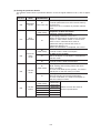
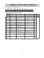
Chapter 8. Error and Treatment
When this board is abnormal, EA, EB, or FT on the LED lights (see page 4-1), and stores error code in
control relay area. (See page 6-13 and App-2.)
The stored address is fixed by module No. switch setting of the module.
Module no. switch specified
0
1
2
3
4
5
6
7
Error code storage address コ0202 コ 0222 コ 0242 コ 0262 コ 0302 コ 0322 コ 0342 コ 0362
Causes and treatments for errors
Error code
(Hexadecimal)
Cause
[(
Treatment
) means page to refer.]
Lighting
LED
—
—
Normal operation
80
Parameter transfer
error
Set other than 22HEX in parameter transfer.
81
BCC calculation
error
Setting value of BCC calculation Check setting value of BCC
value. (6-5)
is incorrect.
82
Communication
mode error
Setting value of communication
mode is outside the range.
Check setting value of communication mode (6-5)
3
Transfer mode error
Setting value of transfer mode is Check setting value of transfer
mode. (6-5)
outside the range.
4
Transfer rate error
Setting value of transfer rate is
outside the range.
Check setting value of transfer
rate. (6-5)
5
Data length error
Setting value of data length is
outside the range.
Check setting value of data
length. (6-6)
6
Stop bit error
Setting value of stop bit is
outside the range.
Check setting value of stop bit.
(6-6)
7
Parity error
Setting value of parity is outside Check setting value of parity.
(6-6)
the range.
8
Control signal error
Setting value of control signal is Check setting value of control
signal. (6-7 to 6-8)
outside the range.
9
89
Transfer code
conversion error
Check setting value of transfer
Setting value of transfer code
conversion is outside the range. code conversion. (6-9 to 6-10)
10
8A
Sending time over
interval error
Setting value of sending time
over interval is outside the
range.
Check setting value of sending
time over interval. (6-11)
11
8B
Receiving time over
interval error
Setting value of receiving time
over interval is outside the
Check setting value of receiving time over interval. (6-11)
12
84
85
86
87
88
—————
8-1
—————
Priority
00
83
Parameter setting error
Name
Check setting value of parameter transfer (6-5)
2
13
EA
Error code
(Hexadecimal)
90
Name
Control relay setting error
Priority
14
Setting value of sending,
receiving header/terminator is
outside the range.
Check control relay settings
of sending, receiving header/
terminator. (6-14)
Number of sending
bytes error
• Setting value of the number of
sending bytes is outside the
range.
• Set sending header/terminator
to "absent," and number of
sending byte setting is
"variable data length."
Check number of sending
byte setting control relay,
sending header/terminator
setting control relay. (6-14)
While number of sending bytes
being "variable data length,"
there is no sending terminator in
sending data.
Check sending data, sending
header/terminator setting
control relay, number of
sending byte setting control
relay, sending header/
terminator setting parameter.
(6-12, 6-14)
17
Number of receiving
bytes error
Setting value of number of
receiving byte is outside the
range.
Check number of receiving
byte setting control relay. (614)
16
Parity error
An error occurs by parity check
during receiving data.
• Check communication
setting with external device.
Number of sending
bytes undefined error
92
A0
Treatment
Sending, receiving
header/terminator
error
91
93
Cause
Lighting
LED
15
EA
19
• Check external device,
communication cable.
A1
Communication error
A2
Framing error
Overflow error
Number of receiving bytes
exceeds 512 bytes which is a
limit to transfer to CPU board.
Check number of sending
data of external device.
Receive unable to convert code
by ASCII −> BIN conversion of
receiving data.
Check sending data of
external device.
When receiving header/
terminator is set to STX-ETX +
BCC, BCC code calculated by
receiving data differs from
received BCC codes.
Check sending data of
external device.
BCC check error
A5
Communica- Hardware
error
tion error
21
Check number of sending
data of external device.
A4
C0
20
Receiving data exceeds
receiving buffer capacity.
Data conversion error
A7
• Check communication
setting with external device.
• Check external device,
communication cable.
Overrun error
A3
A6
Receiving data is abnormal.
EB
Sending time over
error
Prohibition to receive of an
external device continued
longer than sending time out
interval set in parameter.
Receiving time over
error
Data stopped condition while
data receiving continued longer
than receiving time out interval
set in parameter.
Hardware error
Error occurs by ROM sum
check, RAM read/write check
inside the module.
Replace this board.
When the transfer mode is half
duplex, both the module and an
external device send data, or
communication cable is shorted.
Check external device,
communication cable.
25
Module error
Watchdog timer timed over.
——
SM3 error
SM3 is set to other than 0.
Set SM3 to 0.
8-2
24
26
——
Data collision error
23
Check external device,
communication cable.
• Check sending, receiving
timing with external device.
• Check communication
cable.
Replace the module
C1
22
1
EA
18
EB
—
FT
EA
EB
—
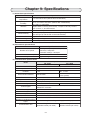
Chapter 9: Specifications
(1) Generaleral specifications
Items
Ambient operation
temperature
Storage temperature
/humidity
Vibration
Shock
Noise immunity
Installation direction
Grounding
Accessories
Specifications
0 to +55oC/35 to 90% (without dew condensation)
-20 to +70oC/35 to 90 %RH (without dew condensation)
JIS C0911 or equivalent
Duplex width: 0.15 mm (10 to 55 Hz), 1 G (55 to 150 Hz), 2 hours
each in the X, Y, and Z directions
JIS C0912 or equivalent. 10 G 3 times in X, Y, and Z directions
1000 Vp-p, 1µs (by noise simulator: Voltage charged between the 24
VDC line (pin 9) and the FG on the motherboard.)
Any of the 3 directions.
Class 3 grounding
4 screws (Semuth M3 x 6 mm), 4 standoffs (15 mm)
(2) Performance specifications
Item
Specifications
I/O relays: 64 points (dummies)
Data relay: 128 points
Parameter settings: 128 bytes
Number of I/O points
Internal current consumption
Weight
210 mA
Approx. 150 g
(3) Communication specifications
Specifications
Items
Number of serial I/F ports
Specifications
Number of connectable
modules
Data transfer standard
Transfer rate
Synchronous mode
Transfer mode
Circuit configuration
Control signal
RS -232C
RS -422A
1 (Use either RS-232C or RS-422A)
No protocol
1 set
Max. 15 sets
EIA RS-422A (2-wire system,
4-wire system)
600, 1200, 2400, 4800, 9600, 19200 bits/sec.
Start-stop system
Full-duplex/half-duplex
1:1
1:N
Absent, RS/CS manual, RS/CS automatic, XON/XOFF manual,
XON/XOFF automatic
7/8 bits
Absent, odd, even
1/2 bits
Absent, EXP1, EXP2, CR, LF, CR - LF, STX, ETX, ETX+BCC
Non-conversion, BIN <-> ASCII conversion
EIA RS-232C
Data length
Parity
Stop bit
Control character
Transfer code
Number of sending/receiving
Individual setting for sending/receiving (1 to 512 bytes)
bytes
Cable total length :Max. 15 m
Cable total length :Max. 1 km
Communication line
(Shielded twisted pair cable)
(Shielded twisted pair cable)
9-1
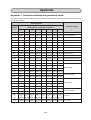
Appendix
Appendix 1. Parameter address and parameter name
The below table shows the relation between address of parameter area and name of parameter set by
module No. switches.
Parameter area
Parameter
address
T-0 to 7
Register address of file 1
(Setting value of module No. switch)
0
1
2
3
5
4
Parameter name
6
7
000
000000 000200 000400 000600 001000 001200 001400 001600 Parameter transfer
001
000001 000201 000401 000601 001001 001201 001401 001601 BCC calculation
002
000002 000202 000402 000602 001002 001202 001402 001602 Communication mode
003
000003 000203 000403 000603 001003 001203 001403 001603 Transfer mode
004
000004 000204 000404 000604 001004 001204 001404 001604 Transfer rate
005
000005 000205 000405 000605 001005 001205 001405 001605 Data length
006
000006 000206 000406 000606 001006 001206 001406 001606 Stop bit
007
000007 000207 000407 000607 001007 001207 001407 001607 Parity
010
000010 000210 000410 000610 001010 001210 001410 001610 Control signal
011
000011 000211 000411 000611 001011 001211 001411 001611 Transfer code conversion
012
000012 000212 000412 000612 001012 001212 01412 001612 Sending time over interval
013
000013 000213 000413 000613 001013 001213 001413 001613 Receiving time over interval
014
000014 000214 000414 000614 001014 001214 001414 001614
015
000015 000215 000415 000615 001015 001215 001415 001615
016
000016 000216 000416 000616 001016 001216 001416 001616
017
000017 000217 000417 000617 001017 001217 001417 001617
020
000020 000220 000420 000620 001020 001220 001420 001620
021
000021 000221 000421 000621 001021 001221 001421 001621
022
000022 000222 000422 000622 001022 001222 001422 001622
023
000023 000223 000423 000623 001023 001223 001423 001623
024
000024 000224 000424 000624 001024 001224 001424 001624
025
000025 000225 000425 000625 001025 001225 001425 001625
026
000026 000226 000426 000626 001026 001226 001426 001626
027
000027 000227 000427 000627 001027 001227 001427 001627
030
to
176
000030 000230 000430 000630 001030 001230 001430 001630
to
to
to
to
to
to
to
to
Not used
000176 000376 000576 000776 001176 001376 001576 001776
177
000177 000377 000577 000777 001177 001377 001577 001777 BCC code
App-1
EXP1 header
EXP1 terminator
EXP2 header
EXP2 terminator
Appendix 2. Address and name of control relay
The below table shows the relation between address of control relay area and name of control relay set by
module No. switches.
Control relay address
(Setting value of module No. switches)
0
1
2
3
4
5
6
Name of control relay
(Bit address)
7
コ0200 コ0220 コ0240 コ0260 コ0300 コ0320 コ0340 コ0360
Signal
D7
D6
D5
D4
D3
D2
D1
D0
direction
––
––
RS
––
RREQ
––
TRDY
––
CPU board -> Z-354J
––
CS
RACK
RRDY
––
TREQ
––
CPU board <- Z-354J
コ0201 コ0221 コ0241 コ0261 コ0301 コ0321 コ0341 コ0361 URDY
Error code
コ0202 コ0222 コ0242 コ0262 コ0302 コ0322 コ0342 コ0362
コ0203 コ0223 コ0243 コ0263 コ0303 コ0323 コ0343 コ0363 Sending header/terminator
Receiving header/
コ0204 コ0224 コ0244 コ0264 コ0304 コ0324 コ0344 コ0364
Number of sending bytes (Lower)
コ0205 コ0225 コ0245 コ0265 コ0305 コ0325 コ0345 コ0365
Number of receiving bytes (Upper)
コ0206 コ0226 コ0246 コ0266 コ0306 コ0326 コ0346 コ0366
Number of transfer bytes (Lower)
コ0207 コ0227 コ0247 コ0267 コ0307 コ0327 コ0347 コ0367
Number of transfer bytes (Upper)
コ0210 コ0230 コ0250 コ0270 コ0310 コ0330 コ0350 コ0370
Number of receiving bytes (Lower)
コ0211 コ0231 コ0251 コ0271 コ0311 コ0331 コ0351 コ0371
Number of receiving bytes (Upper)
コ0212 コ0232 コ0252 コ0272 コ0312 コ0332 コ0352 コ0372
to
to
to
to
to
to
to
to
コ0217 コ0237 コ0257 コ0277 コ0317 コ0337 コ0357 コ0377
Not used
App-2
CPU board -> Z-354J
CPU board <- Z-354J
CPU board -> Z-354J
–––––
SHARP MANUFACTURING SYSTEMS CORPORATION
♦ Information about Sharp image sensor camera and programmable controller
is available at our internet homepage
http://sharp-world.com/sms/
1.0v
10.2005
(0.1I.M.S)