1
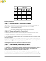
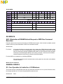
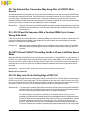
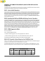
MPC823 Device Errata MPC823 Silicon Revision A—Mask Set 0H89G, 1H89G March 30, 2000 (Version 5) These errata apply to the MPC823 Revision A (CDR2) silicon. Those errata that are currently scheduled to be addressed in the future revision of the silicon are so marked. Notice that this device has soft modem specific microcode installed. There are errata that carry over from the Revision 0.x silicon and may be renumbered here. Changes to this errata are in italics. CPU ERRATA CPU1. Bus Error Not Fully Supported by the Data Cache on a Burst The data cache does not support a bus error that might occur on the second or third data beat of a burst. (burt_232). Workaround: Avoid using a bus error in this case. CPU2. Incorrect Data Breakpoint Detection on Store Instructions When a breakpoint on data occurs and you have programmed the size elements as byte or half-word, the following may occur: • A breakpoint might be detected when it should not • A breakpoint might not be detected when it should Either of these two cases can occur if the data that is programmed to be detected, matches some other portion of the register that is currently stored to memory by the store byte or store half-word instruction. For example: • Assume that you have programmed a byte data breakpoint on a store instruction and you are looking for the byte element 0x55. Assume that register R1 has the value 0x00080000, R10 has the value 0x55443322, and the stb R10,0x3(R1) store instruction is performed. What occurs is that byte 0x22 from R10 is stored to address 0x00080003, and this should not generate a breakpoint since 0x22 does not equal 0x55, but, in some cases, it can and does (in this scenario, R10 does include the data 0x55). The result is a breakpoint is executed when it should not be. This document contains information on a product under development. Motorola reserves the right to change or discontinue this product without notice. SEMICONDUCTOR PRODUCT INFORMATION 2000 Motorola, Inc.All Rights Reserved. • Assume that in the above case you are programming for byte element 0x22, maybe a breakpoint condition will not be detected, even though it should. (burt_246) Note: Workaround: These fault cases depend on the previous Load-Store instruction address. If the previous Load-Store instruction address’ LSB is different from the current instruction address’ LSB, then an incorrect breakpoint detection might occur. None. CPU3. Program Trace Mechanism Error In the following cases, there is an error in the program trace mechanism: • 0x00004ff0: divw. r25,r27,r26 • 0x00004ff4: divw. r28,r27,r26 • 0x00004ff8: unimplemented • 0x00004ffc: b 0x00005010 • and where: 0x00005010 belongs to a page where a page fault occurs The divide takes a relatively long time, so the instruction queue gets filled with the unimplemented instruction, which is the branch and the branch target (page fault). When the sequencer takes the unimplemented instruction, it releases the fetch that was blocked by the mmu error, which causes the queue to get another instruction in addition to the first page fault. Because the second fault is sequential to the branch target, it is not reported by the queue flush (VF) and this causes an incorrect value to be present in the VF flush information when the unimplemented exception occurs. (burt_251) Workaround: None. CPU4 Case of I-Cache Using Address of Old Page When Fetching New Page. The Instruction Cache uses the address associated with the old page when fetching the first data from a new page, under the following circumstances. 1.)There is a show cycle on a sequential instruction which crosses the page boundary. 2.)The internal bus is busy during the IMMU request with the old page number. Thus on the next cycle the I-Cache uses this incorrect address to access the external memory and internal cache. (burt_285) Workaround: Do not run in “show all” mode or do not put a sequential instruction in the last address of an MMU page. cpu5. Doesn’t apply to this silicon cpu6. Doesn’t apply to this silicon cpu7. Doesn’t apply to this silicon CPU8. Possible Error in Instruction Execution with Branch Prediction 2 MPC823 DEVICE ERRATA (REV. A) MOTOROLA and Sequential Branch Instructions. IF there are three branches in sequence in the run-time program flow AND the third branch is in the mis-predicted path of the second branch, THEN although the third branch is part of a predicted path, it may be "issued" from the instruction queue. If this instruction issue in the mis-predicted path happens at the same time that the condition of the prediction is resolved (thereby causing mis-predicted instructions to be flushed from the instruction queue), then the resulting instruction cancellation will back up too far into the instruction queue. This will cause the instruction sequence starting from the instruction immediately preceding the first branch to be re-issued. (burt_305) Note: 1) Other factors of the internal state of the core also affect the occurrence of this behavior. Therefore, not all occurrences of this instruction sequences necessarily exhibit this behavior. 2) This behavior is not necessarily harmful to the user application. For example, the instruction preceding the first branch could be a simple move between registers. 3) Not all compilers generate this instruction sequence. The following compilers are known never to generate code that is susceptible to this erratum: Diab Data (all versions) and Metaware. We are continuing to investigate other compilers with their vendors; their status is unknown at this time. We will update this list as our investigation progresses. Workaround: For every conditional branch preceded in program order by another branch: 1) IF the two possible targets of the conditional branch consist of a branch instruction and a non-branch instruction THEN force the prediction of the conditional branch to predict the non-branch instruction (using the ybit in the opcode of the conditional branch). 2) IF both of the possible targets of the conditional branch are branch instructions THEN insert a non-branch instruction before the branch on the predicted path OR insert an 'isync' instruction before the first branch. CPU9. Branch From Last MMU Page to Last Instruction in Other Page. If a branch from last instruction of an MMU page is performed to a last instruction of another MMU page, Then the first instruction at the target of the branch (The last instruction in the target MMU page) is skipped (i.e. it is not executed). A MMU page is defined as naturally aligned 4K page. If the MMU is disabled, then this behavior happens when Instruction cache is active and not serialized mode. (burt_306) Workaround: Avoid branches form last instruction of page to last instruction of another page. CPU10. Instruction Sequencer Error When Modifying MSR With Interrupts Enabled. IF the following instructio n sequence occurs: mtmsr Rx # change IR (Instruction Relocate) bit or PR (Problem # State) bit in MSR MOTOROLA MPC823 DEVICE ERRATA (REV. A) 3 op1 op2 AND external interrupts were previously enabled (or are being enabled by this mtmsr instruction) AND an external interrupt or decrementer interrupt occurs (or is already pending) AND op1 not in the Instruction cache AND the first instruction in the interrupt handler is fetched at the same clock that the op2 instruction is prefetched from external memory (as seen on the internal bus) THEN the sequencer takes op2 as the first instruction in the interrupt handler. Also the sequencer and Instruction cache are out of sync in subsequent instruction fetched in the interrupt handler until a change of flow is executed. (“Change of flow” can also be isync and mtmsr commands.) Workaround: Do not execute mtmsr that changes IR or PR bits when external interrupt (and decrementer interrupt) are enabled (i.e. when MSR[EE]=1). Allow at least two sequential instructions after the mtmsr that changes IR or PR before enabling interrupts. CPM ERRATA CPM1. Port A Pin (PA13) May Consume Excess Current When the Port A pin PA13 is configured as the SCC2 function RXD2 and the IrDA logic is not enabled (i.e.,the EN=0 in the IRMODE register), then the MPC823 may consume excess current due to internal contention after entering low power modes. Other than the approximate 1mA of excess current, there are no operational issues. This current consumption is most noticeable in the lower power modes. Workaround: Before entering deep-sleep mode, configure PA13 as a general-purpose input. When you exit deep-sleep mode, reconfigure PA13 as the SCC2-controlled RXD2, as required. Will be fixed in revision B. CPM2. Improper Initialization May Cause Excess Current Consumption An initialization problem in the USB block might cause excess current in the deep-sleep mode. This current consumption is most noticeable in the lower power modes. Workaround: As part of the power-on initialization sequence, the software should enable the baud rate generator clock1 (BRGC1) by setting the EN bit to 1 and leaving it set for at least 16 system clocks before changing the serial interface clock route register from its default value (0x00000000). Will be fixed in revision B. CPM3. I2C Master Fails to Receive After Executing Read or Write If the I2C channel is in master mode, after the I2C channel performs a transaction (read or write command), the I2C channel will fail to receive a transmission from another master. It will respond with NACK.Furthermore, after the failed reception, if the I2C master then attempts to perform another transaction (read or write command), the transaction will fail with an underrun error. Workaround: 4 After the master I2C channel completes its transmission, disable and re-enable the channel in the I2MOD register (thereby resetting it). MPC823 DEVICE ERRATA (REV. A) MOTOROLA Will be fixed in revision B. CPM4. I2C Receives Single-Byte Buffers After Failed Transaction A. If the I2C channel is in master mode, then: IF the I2C master attempts a transaction (read or write command) which receives a NACK, AND the I2C master then attempts to execute a read to another slave, THEN the master will receive the first byte of the slave’s message in one buffer and will close the BD, and then will continue to receive the rest of the message in the next BDs. This reception of the first byte in a single-byte buffer will happen regardless of the MRBLR B. If the I2C channel is in slave mode, then: IF the I2C slave responds to a read command (i.e. performs a transmission), AND the I2C slave then responds to a write command THEN the v slave will receive the first byte of the master’s message in one buffer and will close the BD, and then will continue to receive the rest of the message in the next BDs. This reception of the first byte in a single-byte buffer will happen regardless of the MRBLR. Workaround: After the I2C channel performs a transmission (master read or write, or slave response to read), disable and re-enable the channel in the I2MOD register (thereby resetting it). Will be fixed in revision B. CPM5. I2C receiver locked, holding the I2CSDA line low The I2C receiver may lock up, holding the I2CSDA line low, in a system that has slow rise/fall time on the I2C clock (I2CSCL) or if the environment is noisy. Workaround: Set the I2C pre-divider to 32 (by setting I2MOD[PDIV]=00), and restrict rise/fall time of I2CSCL to 0.5 microseconds. Will be fixed in revision B. CPM6. Assignment of Timer Pairs to Port B Pins for Pulse-Width Modulation Channels Changed The RISC timer pairs that are connected to the Port B pins for Pulse-Width Modulation are different from revision 0.x silicon. The following table shows the differences. MOTOROLA MPC823 DEVICE ERRATA (REV. A) 5 TIMER PAIRS PIN MPC823 REV. 0.X MPC823 REV. A MPC823 REV. B PB[23] 0, 1 0, 1 0, 1 PB[22] 2, 3 4, 5 2, 3 PB[19] 8, 9 6, 7 8, 9 PB[18] 10, 11 10, 11 10, 11 PB[17] 12, 13 12, 13 12, 13 PB[16] 14, 15 14, 15 14, 15 Will be fixed in revision B. CPM7. I2C Receive Problem in Arbitration-Lost State If the MPC821 I2C master transmitter loses arbitration to another I2C master which is transmitting to the MPC821, the 821 receiver will not accept the message (address byte not acknowledged). Workaround: 1. Avoid multimaster configuration 2. The operation should be retried by the other master through software. CPM8. I2C Master Collision After ‘Double Start’. The following situation will result in the I2C controller colliding with the transmission of another master: 1) Another I2C master performs a ‘master write’ to the I2C controller of the MPC821. 2) The I2C controller of the MPC821is waiting for the I2C bus to become idle in order to become the master and perform a transaction. 3) The other I2C master asserts a new ‘START’ condition without asserting a ‘STOP’ condition. In this case, the I2C master of the MPC821 will incorrectly interpret the new ‘START’ condition as generated by itself, and will therefore drive the I2C bus concurrently with the other master. Workaround: Avoid performing back-to-back START conditions on the I2C bus. CPM9. I2C Short Aborted Transmission After NACK. The following situation will cause the I2C controller of the MPC821 to send a short aborted transmission: 1) The MPC821’s I2C controller performs a transaction, transmitting a buffer which has no STOP condition at the end. The next buffer (not yet transmitted) will issue a START condition, producing back-to-back transactions without an intervening STOP (also known as ‘double start’). 2) The MPC821’s I2C controller receives a NACK on the last or next-to-last byte of the buffer. If this case occurs, then the MPC821’s I2C controller will assert a STOP condition (as expected by the I2C protocol). However, when software subsequently issues a new start command (I2COM = 0x81), the I2C master will begin 6 MPC823 DEVICE ERRATA (REV. A) MOTOROLA its next transaction erratically. It will issue a START condition and drive one bit of the message, then drive a new START condition and restart the transmission (including the first bit). Workaround: Do not set up the MPC821’s I2C controller to perform ‘double start.’ CPM10. I2C Split Receive Buffer Between Loopback and Read. IF the MPC821’s I2C master performs a loopback transaction (i.e. a master write to its own I2C address or a master write to the General Call address with General Call reception enabled). AND the MPC821’s I2C master then performs a master read transaction THEN the receive buffer used for the loopback transaction will not be closed after the loopback transaction. Instead, it will be closed after the first byte of the read transaction is received. Thus, the received data from the read transaction will be split between the loopback buffer and the intended receive buffer. Workaround: Avoid performing loopback transactions during normal operation. CPM11. I2C Spurious BUSY Errors After Reception in I2C Master Mode. IF the MPC821’s I2C controller is configured as an I2C master AND the I2C controller is the target of another master’s write, THEN after the MPC821 receives the data from the master (and thus closes the receive buffer appropriately), it will attempt to open the next receive buffer (even though there is no receive data). If there is no buffer available, it will generate a BUSY error. Workaround: Ignore BUSY errors in this case. CPM12. Aggressive Mode Frequency Limitation The use of aggressive mode (as determined by the LAM, RAID and LAID fields of the SDCR, page 16-87 of the MPC823 UM) is not recommended for use above waiting on response. If used above waiting on response unexpected behavior will result. This behavior is caused by edge conflicts in the internal logic for this mode of operation. CPM13. USB NACK (threshold) Problem get information from emails. waiting on more details from Yehuda. I think these should be two separate errata. 1) transmission from endpoint is conditioned by the transmit fifo reaching a certain water mark. If the condition is not met, the endpoint response with NACK. This will eliminate the underrun problem, and the workaround sequence. 2) an endpoint that responds with NACK (transmit data not ready) will not set the TXE (Transmit Error) interrupt. The fix will also eliminate the problems with fifo flush that were caused as side effect. 3) the design will be more robust for detecting the start of a packet. We had problems with some PCs that drove the D+ and D- lines asymmetrically. MOTOROLA MPC823 DEVICE ERRATA (REV. A) 7 Workaround: workaround for the underrun problem : should implement the following procedure for FIFO flush: 1. issue a stop_transmit host command via CPCR. 2. (clear the ready bit (R) of the current Tx BD). 3. issue the flush command. when you are ready to send the new packet: 1. setup the new Tx BD list 2. set the endpoint to ignore IN 3. issue a restart_tx command via CPCR 4. set the STR bit to fill the fifo 5. delay, then return to normal handshake mode. fifo fill workaround : - configure the port to ignore IN token - set the BD ready bit - set STR bit - delay ~4us (short loop to insure the fifo is filled with enough data) - return to normal handshake mode CPM14. RCCR and RMDS Should Be Written To As A Single 32-bit Register The ERAM4K bit is cleared in the RISC Microcode Development Support Control Register, RMDS, if the register’s location is accessed as either part of a half-word or byte access. Workaround: If the ERAM4K is to be set, the RMDS must be accessed as part of a word starting at IMMR+0x9C4 to IMMR+0x9C7. It is best to write to these two registers as if they were a single 32-bit register. See register table below. 8 MPC823 DEVICE ERRATA (REV. A) MOTOROLA RCCR-RMDS BIT FIELD 0 1 2 3 4 TIME RES 5 6 7 8 9 TIMEP DR2M DR1M 10 11 12 13 14 15 DRQP EIE SCD ERAM RESET 0 0 0 0 0 0 0 0 0 R/W R/W R/W R/W R/W R/W R/W R/W R/W R/W 28 29 ADDR BIT (IMMR & 0xFFFF0000) + 0x9c4 16 17 18 19 20 21 22 23 24 25 26 27 FIELD RESERVED ERAM4K RESERVED RESET 0 0 0 R/W R/W R/W R/W ADDR 30 31 (IMMR & 0xFFFF0000) + 0x9c6 SIU ERRATA SIU1. Elimination of DRAM Refresh Request or MCR Run Command Execution External master access may cause elimination of a DRAM refresh request. Also if refresh is enabled, external master access may cause elimination of MCR run command execution Workarounds: For refresh: If the system includes an external master on the system bus, DRAM refresh should be done by software. This can be accomplished by using the Periodic Interrupt Timer with an interrupt service routine which activates a DRAM refresh pattern from the UPM via a RUN command in Memory Command Register (MCR) of the memory controller. In this case, the hardware refresh mechanism of the memory controller should be disabled. For other MCR run commands (e.g. initializing SDRAM): If the system includes an active external master on the system bus, then make sure hardware refresh is disabled. Will be fixed in revision B. GENERAL ERRATA G1. Core Operation Is Limited to a 3.0V Minimum The current versions of the MPC823 silicon are only tested and verified at 3.0V–3.6V power. Because of this, low voltage operation at 2.2V cannot be guaranteed to power the core. Workaround: MOTOROLA None. MPC823 DEVICE ERRATA (REV. A) 9 G2. The External Bus Transaction May Hang After a PLPRCR Write Access An endless external bus transaction can occur on the next external bus access after executing a PLPRCR write command that changes the MF field. The PLPRCR write command causes the PLL to freeze the clocks until it is locked again, according to the new MF value. The failure mechanism occurs because the clock unit indicates operation complete before all necessary tasks are actually completed. The next external bus request is driven by the system interface unit and suddenly all clocks are stopped. Workaround: The store instruction to the PLPRCR register should be in a burst-aligned address (cache line) followed by an isync instruction. The instruction cache should be enabled while executing this code sequence. G3. LCD Off and On Sequence With a Pending SDMA Cycle Causes Wrong Data Fetch If the LCD controller is turned off and there is a pending SDMA cycle for the LCD controller, and then the LCD is turned on again before the SDMA cycle completes, the LCD controller will start fetching from the start address + 16 instead of the start address. Workaround: Make sure that the pending SDMA cycle is completed before turning on the LCD controller. This can be done by performing an access to external memory before turning on the LCD controller. G4. EXTCLK and CLKOUT Clocks May Not Be In Phase In Half Bus Speed Mode When the MPC823 uses EXTCLK as an input clock source and MF=2 in the PLPRCR (i.e., the frequency of EXTCLK is 1/2 of the internal clock) and the half bus speed mode is used (EBDF=1 in the SCCR), the output clock from CLKOUT could be 180° out of phase from the input clock. This will affect synchronous designs in which the same clock source (EXTCLK) is shared between the MPC823 and another synchronous device. (burt 293) Workaround: Use the CLKOUT as the only source clock to all synchronous devices. Will be fixed in revision B. G5. PLL May Lock On the Falling Edge of EXTCLK The PLL of the MPC823 locks on the falling edge of the input clock EXTCLK. This will affect the skew between EXTCLK and CLKOUT at the rising edge. The skew depends on the duty-cycle of the input clock, but a 50% duty-cycle will not exceed 2nS. This will affect synchronous designs in which the same clock source is used as an input to EXTCLK, as well as to an external synchronous device (a peripheral or ASIC). Workarounds: 1) In cases where multiple external devices need to operate synchronously with the MPC823, use the CLKOUT pin of the MPC823 as the clock source for all external synchronous devices. CLKOUT is the effective system master clock to be used for distribution. 2) In cases where it is necessary to synchronize an external master clock (e.g. from a backplane), an MPC823 and external peripherals to allow data transfers in all three directions, insert a PLL between the external master clock and the EXTCLK pin of the MPC823. Connect the phase comparison pin of the PLL to the CLKOUT pin of the MPC823. Also use the CLKOUT signal as the reference clock for distribution to the local external peripherals. The PLL device used has to be capable of operating with a permanent offset of -2nS, so the range 10 MPC823 DEVICE ERRATA (REV. A) MOTOROLA of lock should extend to about -4nS. NOTE: This workaround is a concept only. It has not been verified in hardware. Will be fixed in revision B. G6. LCD Controller Off Sequence When LAM Bit Is Set May Cause the CPU to Lock Up The LCD aggressive mode (LAM) bit of the SDCR register allows aggressive arbitration for the LCD controller when doing DMAs to system memory. If this bit is set and the LCD controller is turned off, the LCD controller generates a spurious request to the SDMA that may cause the CPU to lockup. Workaround: Clear the LAM bit before turning off the LCD controller. G7. Possible External Bus Hang Occurs Under Certain Error Conditions The external bus cycle may hang when the following sequence of events occur: 1. The transaction on the external bus ends as a result of TEA assertion OR a bus monitor timeout occurs. AND 2. The next transaction also ends with a TEA assertion or a bus monitor timeout. (burt 300) Workaround: None. G8. Higher Than Normal Current Consumption Without Executing a MULLW instruction In the integer multiply module in the core, there are internal latches that do not get initialized properly during reset. Due to this improper initialization there is a 1:8 chance of a driver contention which may create higher than normal current consumption in various modes. This current consumption is most noticeable in the lower power modes. (burt_361) Workaround: Adding a mullw instruction puts the two control lines into a valid state, eliminating the contention. G9. DOESN’T APPLY TO THIS SILICON. G10. DOESN’T APPLY TO THIS SILICON. G11. DOESN’T APPLY TO THIS SILICON. G12. Incorrect Reporting of Loss-of-Lock Reset Status. The RSR[LLRS] bit is set by both unintentional and software-initiated loss-of-lock. The RSR[LLRS] bit should be set only by an unintentional loss-of-lock. Software-initiated loss-of-lock (e.g. changing the SPLL multiplication factor or entering low-power modes) should not set this bit. Workaround: The PLPRCR[SPLSS] functions as intended. Reference this bit instead. G13. Conflict Between Data Show Cycles and SDMA Burst Writes. IF data show cycles are enabled via SIUMCR[DSHW] ANDan internal register or dual-port RAM access is made immediately following an SDMA burst write, THEN the SDMA burst write may be corrupted. The observed phenomenon is that a burst write with four operands will hold the second MOTOROLA MPC823 DEVICE ERRATA (REV. A) 11 operand into the third and fourth burst beats. For example, a burst write of A-B-C-D will be observed on the bus as A-B-B-B. Note: This behavior can also occur when the SDMA burst is to burst-inhibited memory. Setting the memory to burst-inhibited will not solve the problem. Workarounds: Do not use data show cycles in a system that performs SDMA bursts. These include systems that use ATM,Fast Ethernet, and memory-to-memory IDMA. G14. CPU Receives A Machine Check After Writing to the PLPRCR The CPU may receive a machine check after writing to the PLPRCR. This error is caused by an extra clock generated by the clock block after the SIU releases the bus. When the internal bus is released the CPU begins a transaction. The CPU’s clocks are then stopped mid-cycle and it never receives the acknowledge from the bus. The failure mechanism occurs due to an internal logic synchronization issue aggravated by memory refreshes performed by the UPM. The problem is only evident when entering and exiting doze mode frequently, such as when using doze to conserve power. The possibility of encountering this problem is small but finite (1 in a million entries). Workaround: Prevent the CPU from getting the bus during the extra clock. To do so you must enable the instruction cache and insert a delay. To calculate how long of a delay is necessary, take the longest bus transaction including memory refresh and PCMCIA (in CPU clocks). The resultant number of clocks must be executed using instructions such as NOP (1 clock), ISYNC (2 clocks) or DIVW (13 clocks). If you use the DIVW instruction, then divide the resultant number by 13 and round up. Then insert this many DIVW instructions (dividing by one) after the isync (see errata G9). If more than 2 DIVWs are required then the additional CACHE lines must be loaded and locked into the ICACHE. For example, If your longest transaction is 16 CPU clocks, then you must add 2 DIVW instructions: .align 16 .global SetPLPRCR SetPLPRCR: addi r5, r0, 1 nop nop nop # these NOPs keep STW CACHE aligned stw r4, PLPRCR(r3) isync divw r4, r4, r5 divw r4, r4, r5 blr G15. Address Bus May Consume Excess Current in Low Power Modes When entering Sleep or Deep Sleep Mode, normally PLPRCR[FIOPD] is set to 1 to enable internal pulldowns on the Address and Data Bus. In some units, the Address Bus pins are not sufficently pulled down. This may cause excess current draw. The Data Bus is not affected. 12 MPC823 DEVICE ERRATA (REV. A) MOTOROLA Workaround: None. Fixed in Rev. B G16. Open Drain Pins Do Not Allow 5 Volt Pullups The Open Drain pins on the MPC823 will not allow external pullups to raise the voltage to the normal levels. Workaround: None. MOTOROLA MPC823 DEVICE ERRATA (REV. A) 13 GENERAL CUSTOMER INFORMATION Although not generally considered to be errata, the following items are guidelines for using the device appropriately. CI-100. External Interrupt Handling For external interrupt pins, if a request signal is a pulse, the interrupt request pin should be configured to “edge detect mode”. This ensures that the interrupt will be recognized even if interrupts are temporarily blocked or disabled by the software. The interrupt service routine (ISR) should clear the edge status flag after the ISR is entered and prior to setting the MSR’s EE bit (if it waits until after the EE bit is set, a second interrupt may be taken). If a request signal is a “standard handshake”, the assertion is asynchronous, but the negation occurs upon request from the ISR. This ensures that the interrupt is taken and the source of the interrupt is known. The timing with respect to the EE bit is the same. To avoid spurious interrupts, interrupt masks should not be set while interrupts might be sent to the core. Likewise, no interrupts should be disabled while the interrupt might be pending at the core. That way, when the core responds to the interrupt request, the request will still be pending and the core can determine the source of the interrupt. To accomplish all of the above, the EE bit should be disabled when masks are set or when interrupt enables are cleared. CI-101. Move to Special Register (mtspr) Access to ICTRL Register If you use mtspr to set the Ignore First Match (IFM) bit of the ICTRL register to 1 at the same time that you set an instruction breakpoint on this instruction, the chip will behave unpredictably. Workaround: Disable instruction breakpoints when setting the IFM bit. CI-102. Concurrent Operation Of Ethernet & I2C or SPI has Overlapping Parameter RAM Tables. When concurrent operation for the Ethernet protocol and either I2C or SPI is set up and used at the same timer, there is an overlap in the parameter RAM. Workaround: There is microcode available that moves the I2C/SPI parameter RAM entries to another location in the dual port RAM. To use this, download the description of the change and the object code file from the website at: http://www.mot.com/SPS/ADC/pps/_subpgs/_etoolbox/8XX/i2c_spi.html. This package is called the MPC8XX I2C/SPI Microcode Package. CI-103. Port A Pins (PA9 and PA11) May Consume Excess Current in Low Power Modes When the Port A pins PA9 and PA11 are configured as General Purpose Outputs, then the MPC823 may consume excess current in Sleep or Deep-Sleep mode due to internal floating nodes. Other than the 1mA of typical excess current, there are no operational issues. Workaround: Before entering Deep Sleep Mode, set PAPAR[DD9,DD11] and PADIR[DR9,DR11] to 1 to configure them as TDM pins. See Section 16.14.3 on page 16-470 of the MPC823 User's Manual. Be sure to read CI04 below. CI-104. PORT A PINS (PA9 AND PA11) MAY CONSUME EXCESS 14 MPC823 DEVICE ERRATA (REV. A) MOTOROLA CURRENT IN LOW POWER MODES WHILE IN TDM MODE When the Port A pins (PA9 and PA11) are configured as TDM pins, the MPC823 may consume excess current in Sleep or Deep Sleep modes. If the TDM is not active these pins are tristated, causing excess current consumption. Other than the 100 uA of typical excess current, there are no operational issues. Workaround: Set SIGMR[ENA] and SIMODE[STZA] to 1 before entering Sleep or Deep Sleep modes. See Section 16.7.5 on page 16-126 of the MPC823 User's Manual. MOTOROLA MPC823 DEVICE ERRATA (REV. A) 15 GENERAL DOCUMENTATION ERRATA ASSOCIATED WITH SILICON OPERATION The following items reflect additional information about the operation of the MPC823 and references made in the MPC823 User’s Manual. Please refer to the manual for clarification. DOC1. Cache-Inhibit Operation In some cases, the last instruction executed from a certain page gets the caching inhibited attribute of the next page when the page change occurs between the time a fetch request was issued to the instruction cache and the time the instruction cache delivers the instruction to the sequencer. Since the instruction cache-inhibit is only used for performance reasons (mostly for not caching very fast memories or pages that include non real-time programs), the performance effect of this feature is negligible. See Section 9 Instruction Cache for more information. (burt_237) DOC2. Updating the DAR and DSISR with Debug Counter Operation If a load/store breakpoint occurs as a result of debug counter expiration when oa machine check interrupt due to an error in a load/store cycle, a data storage interrupt, or an alignment interrupt occurs, set the DAR and DSISR registers to the effective address associated with the interrupting instruction. In some cases, when a load/store breakpoint occurs when one of the debug counters expires just before one of the above interrupts occur, the value of the DAR and DSISR is changed. Although the interrupt is after the breakpoint and, therefore, should be ignored by the processor, the DAR and DSISR are updated. The value of the DAR and DSISR is normally used by the software inside these interrupt routines and may influence program flow only if these interrupts are nested one inside the other and a load/store breakpoint is used inside one of these interrupt routines. See Section 6 Core and Section 20 Development Support for details. (burt_253) DOC3. SDMA Aggressive Mode Bit 25 of the SDCRLAM: LAM - LCD(Video) Aggressive Mode 0 = Disable LCD/Video aggressive mode. Priority depend on the LAID field. 1 = Enable LCD/Video aggressive mode. The LAID and RAID fields must be equal to 00. This bit affects all SDMA transfers including LCD and Video Controller transfers. D0C4. XFC Capacitor Values Based on the PLPRCRMF Field Table 5-4. XFC Capacitor Values Based on the MF Field in the PowerPC MPC823 User’s Manual on page 523 shows the recommended values for UDR2 (MPC823 rev. 0) silicon. The following table shows the recommended values for the XFC Capacitor for CDR2 (MPC823 rev. A and later) silicon, along with the minimum and maximum values, as determined by the multiplication factor (MF). XFC CAPACITOR VALUES 16 MF RANGE MINIMUM CAPACITANCE RECOMMENDED CAPACITANCE MAXIMUM CAPACITANCE UNIT MF =< 4 580 *MF - 100 680 * MF - 120 780 * MF - 140 pF MPC823 DEVICE ERRATA (REV. A) MOTOROLA XFC CAPACITOR VALUES MF RANGE MINIMUM CAPACITANCE RECOMMENDED CAPACITANCE MAXIMUM CAPACITANCE UNIT MF > 4 830 * MF 1100 * MF 1470 * MF pF DOC5. I2C Address Register Not Cleared on Reset The I2C Address Regsiter (I2ADD) is not cleared by reset. This may cause a nonzero value to be present on reset. If this value matches the address of a slave device on the I2C bus, it will cause reception problems over I2C. This errata has no other effect on operation. Workaround: If using I2C Master Mode, reset I2ADD to 0x0 during your I2C initialization routine. MOTOROLA MPC823 DEVICE ERRATA (REV. A) 17