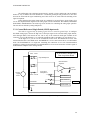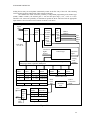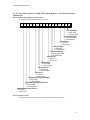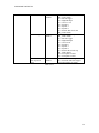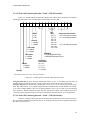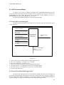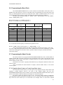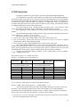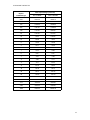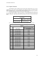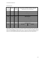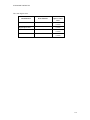
1
PCI4520/DM7520/DM7530
PCI4520
DM7520
DM7530
User’s Manual
Version 2.0
PCI4520 -High-speed Bus Master 12bit Analog Data Acquisition Slot
Board for IBM PC AT with PCI bus
DM7520 - High-speed Bus Master 12bit Analog Data Acquisition
PC/104plus Board with McBSP for DSP communication
DM7530 - Bus Master 16bit Analog Data Acquisition PC/104plus Board
with McBSP for DSP communication
EPLD versions:
PCI4520 – V.7.
DM7520 - V.13.
DM7530 - V.13.
7520v20
3/21/2003 2:09 PM
®
USA
ISO9001 and AS9100 Certified
1
PCI4520/DM7520/DM7530
REAL TIME DEVICES USA, INC.
103 Innovation Blvd
State College, PA 16803
Phone: +1-814-234-8087
FAX: +1-814-234-5218
E-mail
[email protected]
[email protected]
web site
http://www.rtdusa.com
2
PCI4520/DM7520/DM7530
Revision History
11.15.01
1.0 New
11.27.01
1.1 with Ver 11 EPLD for free running D/A clock to be software compatible with the
previous versions
01.07.02
1.2 McBSP control address fix
04.11.02
1.3 DM7530 extension
05.06.02
1.4 DM7530 EPLD ver12. For DM7530
06.28.02
1.5 PCI4520 Timer-counter description fix
01.03.03
1.6 Extension of the sample counter description.
03.18.03
2.0 Updated for the new EPLD Ver13.
Publication PCI4520/DM7520/DM7530 V2.1 2003.04.01
Published by:
Real Time Devices USA, Inc.
103 Innovation Boulevard
State College, PA 16803
Copyright 2001 by Real Time Devices, Inc.
All rights reserved
Printed in U.S.A.
The Real Time Devices USA Logo is a registered trademark of Real Time Devices USA. dspModule,
cpuModule, and utilityModule are trademarks of Real Time Devices USA. PC/104 is a registered
trademark of PC/104 Consortium. TMS320C62x, VelociTI, and C62x are trademarks of Texas
Instraments. All other trademarks appearing in this document are the property of their respective owners.
3
PCI4520/DM7520/DM7530
1. OVERVIEW ..................................................................................................................................... 10
1. OVERVIEW ..................................................................................................................................... 10
1.1. ANALOG-TO-DIGITAL CONVERSION ................................................................................................. 11
1.2. DIGITAL-TO-ANALOG CONVERSION ................................................................................................. 12
1.3. TIMER/COUNTERS ............................................................................................................................ 12
1.4. DIGITAL I/O ..................................................................................................................................... 12
1.5. HIGH-SPEED DIGITAL INPUT ............................................................................................................ 12
1.6. SYNCBUS ......................................................................................................................................... 13
1.7.MCBSP MULTI-CHANNEL BUFFERED SERIAL PORT .......................................................................... 13
1.8. WHAT COMES WITH YOUR BOARD .................................................................................................. 13
1.9. BOARD ACCESSORIES ....................................................................................................................... 13
1.10. HARDWARE ACCESSORIES ............................................................................................................. 13
1.11. USING THIS MANUAL ..................................................................................................................... 13
1.12. WHEN YOU NEED HELP ................................................................................................................. 13
2. INSTALLATION ............................................................................................................................. 15
2.1. BOARD INSTALLATION ..................................................................................................................... 15
2.2. EXTERNAL I/O CONNECTIONS .......................................................................................................... 16
2.3. CONNECTING THE ANALOG INPUT PINS............................................................................................ 19
2.3.1. Ground Referenced Single-Ended (GRSE) input mode............................................................ 20
2.3.2.Non Referenced Single-Ended (NRSE) input mode................................................................... 21
2.3.3. Differential (DIFF) input mode................................................................................................ 22
2.4. CONNECTING THE ANALOG OUTPUTS .............................................................................................. 23
2.5. CONNECTING THE TIMER/COUNTERS AND DIGITAL I/O ................................................................... 23
2.6. CONNECTING THE SYNCBUS ............................................................................................................ 23
2.7. CONNECTING THE MCBSP ............................................................................................................... 24
3. HARDWARE DESCRIPTION ....................................................................................................... 25
3.1. THE OPERATION OF ANALOG INPUT AND HIGH-SPEED DIGITAL INPUT SECTION ............................. 25
3.1.1. Overall Description.................................................................................................................. 25
3.1.2 Channel Gain Latch (CGL) and Channel Gain Table (CGT) ................................................... 25
3.1.3. A/D Converter .......................................................................................................................... 27
3.1.4. A/D FIFO - Sample Buffer ....................................................................................................... 27
3.1.5. Data Transfer ........................................................................................................................... 27
3.1.6. High-Speed Digital Input section ............................................................................................. 28
3.2. THE OPERATION OF ANALOG OUTPUT ............................................................................................. 28
3.3. TIMER/ COUNTERS ........................................................................................................................... 29
3.4. DIGITAL I/O ..................................................................................................................................... 29
3.5. SYNCBUS ......................................................................................................................................... 29
4. REGISTER ADDRESS SPACES OF PCI4520/DM7520/DM7530.............................................. 30
4. 1. LOCAL ADDRESS SPACE 0 (LAS0) - RUNTIME AREA...................................................................... 31
4.1.1. Local Address Space 0 + 000h: Read Master / Target Only mode jumper (JP1) / Firmware
version number - DM7520/DM7530 Only (Read only)...................................................................... 33
4.1.2. Local Address Space 0 + 008h: User Input read / User Output Write (Read/write) ............... 33
4.1.3. Local Address Space 0 + 010h: FIFO Status Register / A/D Conversion Start (Read/write).. 35
4.1.4. Local Address Space 0 + 014h: Software update D/A1 (Write only)....................................... 36
4.1.5. Local Address Space 0 + 018h: Software update D/A2 (Write only)....................................... 36
4.1.6. Local Address Space 0 + 024h: Simultaneous Software Update D/A1 and D/A2 (Write only)36
4.1.7. Local Address Space 0 + 028h: Pacer Clock Software Start trigger / Pacer Clock Software Stop
trigger (Read/Write) ........................................................................................................................... 36
4.1.8. Local Address Space 0 + 02Ch: Pacer and Burst Clock Timer Status Register / Software Highspeed Input Sample command (Read/Write) ...................................................................................... 37
4
PCI4520/DM7520/DM7530
4.1.9. Local Address Space 0 + 030h: Interrupt Status/Mask Register Read/write).......................... 38
4.1.10. Local Address Space 0 + 034h Interrupt Clear Register (Read/Write) ................................. 41
4.1.11. Local Address Space 0 + 038h: Interrupt Overrun Register (Read/Write)............................ 42
4.1.12. Local Address Space 0 + 040h, Pacer Clock Counter (Read/Write) .................................... 43
4.1.13. Local Address Space 0 + 044h, Burst Clock Counter (Read/Write) ...................................... 43
4.1.14. Local Address Space 0 + 048h, A/D Sample Counter (Read/Write)...................................... 44
4.1.15. Local Address Space 0 + 04Ch, D/A1 Update Counter (Read/Write) ................................... 44
4.1.16. Local Address Space 0 + 050h, D/A2 Update Counter (Read/Write).................................... 45
4.1.17. Local Address Space 0 + 054h, Delay Counter (Read/Write) ............................................... 45
4.1.18. Local Address Space 0 + 058h, About Counter (Read/Write) ............................................... 45
4.1.19. Local Address Space 0 + 05Ch, DAC Clock Counter (Read/Write) ...................................... 46
4.1.20. Local Address Space 0 + 060h, 064h, 068h: User Timer/Counter 0, 1, 2 (Read/Write) ...... 46
4.1.21. Local Address Space 0 + 06Ch User Timer/Counter control word (Write Only).................. 47
4.1.22. Local Address Space 2 + 070h - Digital I/O chip Port 0, Bit Programmable Port (Read/Write)
............................................................................................................................................................ 47
4.1.23. Local Address Space 0 + 074h - Digital I/O chip Port 1, Byte Programmable Port (Read/Write)
............................................................................................................................................................ 48
4.1.24. Local Address Space 0 + 78h - Read/Program Port 0 Direction/ Mask/ Compare Registers
(Read/Write) ....................................................................................................................................... 48
4.1.25. Local Address Space 0 + 07Ch - Read Digital IRQ Status/Program Digital Mode (Read/Write)
............................................................................................................................................................ 50
4. 2. LOCAL ADDRESS SPACE 0 (LAS0) - SETUP AREA .......................................................................... 51
4.2.1. Software Reset of the board - LAS0 + 100h (Write Only)........................................................ 61
4.2.2. DMA0 Request Source Select - LAS0 + 104h (WriteOnly) ...................................................... 61
4.2.3. DMA1 Request Source Select - LAS0 + 108h (WriteOnly) ...................................................... 61
4.2.4. Reset DMA0 Request machine - LAS0 + 1CCh (WriteOnly) ................................................... 61
4.2.5. Reset DMA1 Request machine - LAS0 + 1D0h (WriteOnly).................................................... 61
4.2.6. A/D Conversion Signal Select - LAS0 + 10Ch (WriteOnly)..................................................... 62
4.2.7. A/D Burst Clock start trigger select - LAS0 + 110h (WriteOnly) ............................................ 62
4.2.8. Pacer Clock start trigger select - LAS0 + 114h (WriteOnly)................................................... 62
4.2.9. Pacer Clock Stop Trigger select - LAS0 + 118h (WriteOnly) .................................................. 64
4.2.10. About Counter Stop Enable - LAS0 + 11Ch (WriteOnly) ...................................................... 65
4.2.11. Pacer Start Trigger Mode select - LAS0 + 120h (WriteOnly)................................................ 65
4.2.12. Sampling Signal for High Speed Digital Input Select - LAS0 + 124h (WriteOnly) ............... 65
4.2.13. Clear High Speed Digital Input FIFO - LAS0 + 128h (WriteOnly)....................................... 65
4.2.14. Clear A/D FIFO - LAS0 + 12Ch (WriteOnly)........................................................................ 65
4.2.15. Write ADC channel gain table - LAS0 + 130h (WriteOnly)................................................... 66
4.2.16. Write ADC channel gain latch - LAS0 + 134h (WriteOnly)................................................... 66
4.2.17. Write Digital table - LAS0 + 138h (WriteOnly) ..................................................................... 67
4.2.18. Enable Channel Gain Table - LAS0 + 13Ch (WriteOnly)...................................................... 67
4.2.19. Enable Digital Table - LAS0 + 140h (WriteOnly) ................................................................. 67
4.2.20. Table Pause enable - LAS0 + 144h (WriteOnly).................................................................... 67
4.2.21. Reset Channel Gain Table - LAS0 + 148h (WriteOnly)......................................................... 68
4.2.22. Clear Channel Gain Table - LAS0 + 14Ch (WriteOnly)........................................................ 68
4.2.23. D/A1 output type / range - LAS0 + 150h (WriteOnly) ........................................................... 68
4.2.24. D/A1 update source - LAS0 + 154h (WriteOnly) ................................................................... 68
4.2.25. D/A1 Cycle Mode - LAS0 + 158h (WriteOnly)....................................................................... 68
4.2.26. Reset D/A1 FIFO - LAS0 + 15Ch (WriteOnly) ...................................................................... 68
4.2.27. Clear D/A1 FIFO - LAS0 + 160h (WriteOnly) ...................................................................... 68
4.2.28. D/A2 output type / range - LAS0 + 164h (WriteOnly) ........................................................... 69
4.2.29. D/A2 update source - LAS0 + 168h (WriteOnly) ................................................................... 69
4.2.30. D/A2 Cycle Mode - LAS0 + 16Ch (WriteOnly)...................................................................... 69
4.2.31. Reset D/A2 FIFO - LAS0 + 170h (WriteOnly)....................................................................... 69
4.2.32. Clear D/A2 FIFO - LAS0 + 174h (WriteOnly) ...................................................................... 69
4.2.33. A/D Sample Counter Source Select - LAS0 + 178h (WriteOnly) ........................................... 70
4.2.34. Pacer Clock Select - LAS0 + 180h (WriteOnly)..................................................................... 70
5
PCI4520/DM7520/DM7530
4.2.35. SyncBus 0 Source Select - LAS0 + 184h (WriteOnly) ............................................................ 70
4.2.36. Enable SyncBus 0 - LAS0 + 188h (WriteOnly) ...................................................................... 70
4.2.37. SyncBus 1 Source Select - LAS0 + 18Ch (WriteOnly) ........................................................... 71
4.2.38. Enable SyncBus 1 - LAS0 + 190h (WriteOnly) ...................................................................... 72
4.2.39. SyncBus 2 Source Select - LAS0 + 198h (WriteOnly) ............................................................ 72
4.2.40. Enable SyncBus 2 - LAS0 + 19Ch (WriteOnly)...................................................................... 72
4.2.41. External Trigger polarity select - LAS0 + 1A4h (WriteOnly) ................................................ 72
4.2.42. External Interrupt polarity select - LAS0 + 1A8h (WriteOnly).............................................. 72
4.2.43. User Timer/Counter 0 Clock Select - LAS0 + 1ACh (WriteOnly).......................................... 73
4.2.44. User Timer/Counter 0 Gate Select - LAS0 + 1B0h (WriteOnly) ............................................ 73
4.2.45. User Timer/Counter 1 Clock Select - LAS0 + 1B4h (WriteOnly) .......................................... 73
4.2.46. User Timer/Counter 1 Gate Select - LAS0 + 1B8h (WriteOnly) ............................................ 73
4.2.47. User Timer/Counter 2 Clock Select - LAS0 + 1BCh (WriteOnly).......................................... 74
4.2.48. User Timer/Counter 2 Gate Select - LAS0 + 1C0h (WriteOnly)............................................ 74
4.2.49. User Output 0 Signal Select - LAS0 + 1C4h (WriteOnly)...................................................... 74
4.2.50. User Output 1 Signal Select - LAS0 + 1C8h (WriteOnly)...................................................... 75
4.2.51. McBSP A/D FIFO control - LAS0 + 1ECh (WriteOnly) ........................................................ 75
4.2.52. McBSP D/A1 and D/A2 FIFO control - LAS0 + 1F0h (WriteOnly) ...................................... 75
4.3. LOCAL ADDRESS SPACE 1 (LAS1)................................................................................................... 76
4.3.1. Local Address Space 1 +0h: Read A/D FIFO (Read only) ...................................................... 77
4.3.2. Local Address Space 1 +4h: Read High Speed Digital Input FIFO (Read only) .................... 77
4.3.3. Local Address Space 1 +8h: Write D/A1 FIFO (Write only)................................................... 78
4.3.4. Local Address Space 1+Ch: Write D/A2 FIFO (Write only) ................................................... 79
5. A/D CONVERSION ......................................................................................................................... 80
5.1. BEFORE STARTING CONVERSIONS: INITIALIZING THE BOARD .......................................................... 80
5.1.1. Before Starting Conversions (single-channel mode): Programming Channel, Gain, Input Range
and Type using Channel Gain Latch (CGL)....................................................................................... 80
5.1.2. Before Starting Conversions (multi-channel mode): Programming the Channel-Gain Table (CGT)
............................................................................................................................................................ 80
5.1.3. 16-Bit A/D Table ...................................................................................................................... 80
5.1.4. Channel Select, Gain Select, Input Range and Input Type....................................................... 81
5.1.5. Pause bit................................................................................................................................... 81
5.1.6. D/Ax update bits ....................................................................................................................... 81
5.1.7. Skip bit...................................................................................................................................... 81
5.1.8. 8-Bit Digital Table.................................................................................................................... 82
5.1.9. Setting Up A/D part and Digital part of Channel Gain Table ................................................. 82
5.1.10. Using the Channel Gain Table for A/D Conversions ............................................................. 82
5.1.11. Channel-gain Table and Throughput Rates ........................................................................... 84
5.2. A/D CONVERSION MODES ............................................................................................................... 85
5.2.1. Start A/D Conversion signal..................................................................................................... 85
5.2.2. Pacer Clock Start/Stop Trigger Select. .................................................................................... 85
5.2.3. Types of Conversions................................................................................................................ 87
5.3. READING THE CONVERTED DATA .................................................................................................... 89
5.4. USING THE A/D DATA MARKERS ..................................................................................................... 90
5.5. PROGRAMMING THE PACER CLOCK .................................................................................................. 90
5.6. PROGRAMMING THE BURST CLOCK .................................................................................................. 91
5.7. PROGRAMMING THE ABOUT COUNTER ............................................................................................. 91
5.7.1. Using the About Counter to Create Large Data Arrays........................................................... 91
6. D/A CONVERSION ......................................................................................................................... 93
6.1. 1024 SAMPLE BUFFER...................................................................................................................... 96
6.2. D/A CYCLED OR NOT CYCLED MODE .............................................................................................. 97
6.3. D/A UPDATE COUNTERS .................................................................................................................. 97
6.4. D/A DATA MARKERS ....................................................................................................................... 97
7. DATA TRANSFER USING DMA .................................................................................................. 98
6
PCI4520/DM7520/DM7530
7.1 NON-CHAINING MODE DMA ............................................................................................................ 98
7.2 CHAINING MODE DMA..................................................................................................................... 98
7.3 DMA DATA TRANSFERS ................................................................................................................... 99
7.3.1 Demand Mode DMA.................................................................................................................. 99
7.3.2. DMA Priority............................................................................................................................ 99
7.4 DMA REGISTERS ............................................................................................................................ 100
7.4.1. (DMAMODE0; PCI:80h) DMA Channel 0 Mode Register.................................................... 101
7.4.2. (DMAPADR0; PCI:84h) DMA Channel 0 PCI Address Register.......................................... 102
7.4.3. (DMALADR0; PCI:88h) DMA Channel 0 Local Address Register ....................................... 102
7.4.4. (DMASIZ0; PCI:8Ch) DMA Channel 0 Transfer Size (Bytes) Register................................. 102
7.4.5. (DMADPR0; PCI:90h) DMA Channel 0 Descriptor Pointer Register .................................. 103
7.4.6. (DMAMODE1; PCI:94h) DMA Channel 1 Mode Register.................................................... 104
7.4.7. (DMAPADR1; PCI:98h) DMA Channel 1 PCI Address Register.......................................... 105
7.4.8. (DMALADR1; PCI:9Ch) DMA Channel 1 Local Address Register....................................... 105
7.4.9. (DMASIZ1; PCI:A0h) DMA Channel 1 Transfer Size (Bytes) Register................................. 105
7.4.10. (DMADPR1; PCI:A4h) DMA Channel 0 Descriptor Pointer Register................................ 106
7.4.11. (DMACSR0; PCI:A8h) DMA Channel 0 Command/Status Register ................................... 106
7.4.12. (DMACSR1; PCI:A9h) DMA Channel 1 Command/Status Register ................................... 107
7.4.13. (DMAARB; PCI:ACh) DMA Arbitration Register ............................................................... 107
7.4.14. (DMATHR; PCI:B0h) DMA Threshold Register.................................................................. 108
8. INTERRUPS................................................................................................................................... 109
8.1. THE OVERRAL INTERRUPT STRUCTURE OF PCI4520/DM7520/DM7530....................................... 109
8.1.1. The Interrupt Sources of PCI4520/DM7520/DM7530........................................................... 109
8.1.2. The Interrupt Registers of PCI4520/DM7520/DM7530......................................................... 110
8.2. THE OPERATION OF ON-BOARD PRIORITY INTERRUPT CONTROLLER ............................................. 111
8.3. ADVANCED DIGITAL INTERRUPTS .................................................................................................. 112
8.3.1. Event Mode............................................................................................................................. 112
8.3.2. Match Mode............................................................................................................................ 112
8.3.3. Sampling Digital Lines for Change of State........................................................................... 112
9. TIMER/COUNTERS ..................................................................................................................... 113
9.1. THE INTERNAL TIMER TIMER/COUNTERS ....................................................................................... 113
9.2. USER TIMER TIMER/COUNTERS...................................................................................................... 113
10. DIGITAL I/O................................................................................................................................ 115
10.1. THE DIGITAL I/O CHIP ................................................................................................................. 116
10.1.1 Port 0, Bit Programmable Digital I/O .................................................................................. 116
10.1.2. Advanced Digital Interrupts: Mask and Compare Registers ............................................... 116
10.1.3. Port 1, Port Programmable Digital I/O ............................................................................... 117
10.1.4. Resetting the Digital Circuitry ............................................................................................. 117
10.1.5. Strobing Data into Port 0..................................................................................................... 117
10.2. HIGH-SPEED DIGITAL INPUT ........................................................................................................ 117
10.3. DIGITAL INPUT DATA MARKERS .................................................................................................. 117
11. CALIBRATION ........................................................................................................................... 118
11.1. REQUIRED EQUIPMENT ................................................................................................................. 118
11.2. A/D CALIBRATION ....................................................................................................................... 118
11.2.1. Bipolar Calibration .............................................................................................................. 118
11.2.3. Unipolar Calibration............................................................................................................ 120
11.2.4. Gain Adjustment ................................................................................................................... 121
11.3. D/A CALIBRATION ....................................................................................................................... 122
12. SPECIFICATIONS ...................................................................................................................... 124
12.1. COMPUTER INTERFACE................................................................................................................. 124
12.2. ANALOG INPUT CIRCUITRY........................................................................................................... 124
7
PCI4520/DM7520/DM7530
12.3. A/D CONVERTER ......................................................................................................................... 124
12.4. A/D SAMPLE BUFFER ................................................................................................................... 124
12.5. CHANNEL GAIN TABLE ................................................................................................................. 125
12.6. CLOCKS AND COUNTERS .............................................................................................................. 125
12.7. DIGITAL I/O ................................................................................................................................. 125
12.8. D/A CONVERTER AND D/A CIRCUITRY ........................................................................................ 125
12.9. D/A SAMPLE BUFFER ................................................................................................................... 125
APPENDIX A - THE PCI CONFIGURATION REGISTERS, LOCAL CONFIGURATION
REGISTERS, RUNTIME REGISTERS, DMA REGISTERS, LOCAL ADDRESS SPACE 0 AND 1
.............................................................................................................................................................. 126
A1. PCI CONFIGURATION REGISTERS ................................................................................................... 133
A.1.1. PCIIDR - Device ID, Vendor ID (PCI CFG offset:00, EEPROM offset:00) ......................... 135
A.1.2. PCICCR - Class Code (PCI CFG offset:09- 0B, EEPROM offset:04) .................................. 135
A.1.3. PCICLSR, PCI LTR, PCI HTR, PCIIPR PCIILR - (PCI CFG offset:0C.. 0E, 3D, 3C, EEPROM
offset:08)........................................................................................................................................... 135
A.1.4. PCISVID - PCI Subsystem Vendor ID (PCI CFG offset:2C, EEPROM offset:44)................ 135
A.1.5. PEROMBA - Expansion ROM PCI Base Address Register(PCI CFG offset:30, EEPROM
offset:54)........................................................................................................................................... 135
A.2. LOCAL CONFIGURATION REGISTERS ............................................................................................. 136
A.2.1. Range for PCI-to-Local Address Space 0 Register (LAS0RR, PCI:00h, EEPROM offset: 14)137
A.2.2 Local Base Address (Remap) for PCI-to-Local Address Space 0 Register (LAS0BA, PCI: 04,
EEPROM offset: 18)......................................................................................................................... 137
A.2.3 Mode/Arbitration Register (MARBR, PCI: 08, EEPROM offset: 1C) .................................... 137
A.2.4 Big/Little Endian Descriptor Register (BIGEND, PCI:0Ch, EEPROM offset: 20h) .............. 138
A.2.5 Expansion ROM Range Register (EROMRR, PCI:10h, EEPROM offset: 24h) ..................... 139
A.2.6 Expansion ROM Local Base Address (Remap) Register and BREQo Control (EROMBA, PCI:14h,
EEPROM offset: 28h)....................................................................................................................... 139
A.2.7 Local Address Space 0/Expansion ROM Bus Region Descriptor Register (LBRD0; PCI:18h,
EEPROM offset: 2Ch) ...................................................................................................................... 140
A.2.8 Local Range Register for Direct Master to PCI (DMRR; PCI:1Ch, EEPROM offset: 30h) .. 141
A.2.9 Local Bus Base Address Register for Direct Master to PCI Memory (DMLBAM; PCI:20h,
EEPROM offset: 34h)....................................................................................................................... 141
A.2.10 Local Base Address Register for Direct Master to PCI IO/CFG (DMLBAI; PCI:24h, EEPROM
offset: 38h)........................................................................................................................................ 141
A.2.11 PCI Base Address (Remap) Register for Direct Master to PCI Memory(DMPBAM; PCI:28h,
EEPROM offset: 3Ch) ...................................................................................................................... 142
A.2.12 PCI Configuration Address Register for Direct Master to PCI IO/CFG (DMCFGA; PCI:2Ch,
EEPROM offset: 40h)....................................................................................................................... 143
A.2.13 PCI Local Address Space 1 Range Register for PCI-to-Local Bus (LAS1RR; PCI:F0h, EEPROM
offset: 48h)........................................................................................................................................ 143
A.2.14 Local Address Space 1 Local Base Address (Remap) Register(LAS1BA; PCI:F4h, EEPROM
offset: 4Ch) ....................................................................................................................................... 144
A.2.15 Local Address Space 1 Bus Region Descriptor Register (LBRD1; PCI:F8h, EEPROM offset:
50h)................................................................................................................................................... 144
A.3. RUNTIME REGISTERS ..................................................................................................................... 145
A.3.1 Serial EEPROM Control, PCI Command Codes, User I/O Control, Init Control ((CNTRL;
PCI:6Ch, no EEPROM loadable) .................................................................................................... 146
A.4. DMA REGISTERS .......................................................................................................................... 146
A.5. LAS0 REGISTER AREA .................................................................................................................. 146
A.6. LAS1 REGISTER AREA .................................................................................................................. 146
APPENDIX B - THE PLX9080 EEPROM CONTENT.................................................................. 147
APPENDIX C - DIFFERENCIES BETWEEN THE PCI4520 AND THE DM7520, DM7530
BOARDS ............................................................................................................................................. 148
8
PCI4520/DM7520/DM7530
LIMITED WARRANTY ................................................................................................................... 149
9
PCI4520/DM7520/DM7530
1. Overview
The PCI4520/DM7520/DM7530 boards turn your desktop PC or PC/104 stack into a high-speed,
high-performance data acquisition and control system. The PCI4520/DM7520/DM7530 bus master
(DM7520/DM7530 can be jumpered to target only mode) DAQ boards are basically equivalent systems.
There are some differences which are discussed in the appropriate place of the manual. There is a list about
the differences in Appendix C.
Boards features:
•
•
•
•
•
•
•
•
•
•
•
•
•
•
•
•
•
•
•
•
•
•
8 differential, 16 single-ended analog input channels,
12-bit, 1.25 Msample/s –DM7520/PCI4520, 16-bit, 100KHz - DM7530 analog-to-digital converter,
Programmable input ranges: +-5, +-10, or 0 to +10 volts, (+-5V range only for DM7530)
Programmable gains of 1, 2, 4, 8, 16, 32, PCI4520 has 64 & 128 gain factors also,
1024 (8192 – optional) x 24 channel-gain scan memory with skip bit,
Software, pacer clock and external trigger modes,
Scan, burst and multi-burst using the channel-gain table,
10/16-bit programmable high speed sample counter and 16-bit delay counter,
1024 / 8192 sample A/D buffer for gap-free full-speed sampling under WindowsTM and DOS
Pre-, post- and about-trigger modes,
8-bit High-Speed Digital Input with 1Ksample FIFO,
8 bit programmable digital I/O lines with Advanced Digital Interrupt modes,
8 bit port programmable digital I/O lines,
24.. 10-bit timer/counters (three software configurable available to user in well known 8254 chip) and
on-board 8 MHz clock,
Two 12/16-bit , 10 microsecond digital-to-analog output channels with 100 kHz throughput,
+-5V, 0 to +5, +-10V, or 0 to +10 Volt (+-10V for DM7530) analog output ranges ,
Two 1024/8192 sample D/A buffers for gap-free full-speed output under WindowsTM and DOS
2-bit analog output data trigger/marker,
three-line SyncBus for synchronized multiboard operation
built-in interrupt priority controller for several simultaneous interrupt source handling,
PCI Busmaster Interface with max. 20MSample/s Burst mode data transfer with built-in two-channel
DMA controller
McBSP for high speed data transfer between the connected dspModule
The following paragraphs briefly describe the major functions of the PCI4520/DM7520/DM7530. A
detailed discussion of board functions is included in subsequent chapters. The Figure 1.1 shows the
simplified block diagram of the board.
10
PCI4520/DM7520/DM7530
SyncBus
Signals
User Clock
User Gate
User Out
McBSP
DSP
connection
Analog
Inputs
3-line
SyncBus
Interface
McBSP
interface
Control Logic
3*16bit User
Timer/
Counter
Analog Input
Multiplexer
Channel
Select
from
CGT
Gain
Select
from
CGT
Sample
clock
Programmable
Gain
(1,2,4,8,16,32,
64,128)
12/16bit
1.25M/500ks/s
A/D
Converter
Pacer clock/
Burst Clock
Timer/
Counter
Digital I/O
Lines (8) P1
A/D, D/A1, Delay, About,
D/A2 Sample
D/A clock
Timer/
Timer/
Counter
Counter
Digital I/O
interface
P1 - byte
programmable
P0 - bit
programmable
Channel
Gain Control
FIFO
1/8KW
Digital I/O
Lines (8) P0
High-Speed
Digital Inputs
Sample
clock
A/D
FIFO
1KW
Analog Outputs
Digital
Sampler
Circuit
Update
clocks
High-Speed
Digital Input
FIFO 1KB
two 12/16bit
10 us
D/A
Converters
D/A1
FIFO
1KW
D/A2
FIFO
1KW
BusMaster PCI Interface
PCI bus
Figure 1.1. PCI4520/DM7520/DM7530 Block Diagram
1.1. Analog-to-Digital Conversion
The PCI4520/DM7520/DM7530 is software configurable on a channel-by-channel basis for up to
16 single-ended (Ground referenced or Non ground referenced) or 8 differential analog inputs. Software
programmable unipolar and bipolar input ranges and gains allow easy interfacing to a wide range of
sensors. Over voltage protection to +-12 volts is provided at the inputs. The common mode input voltage
for differential operation is +-10 volts.
A/D conversions are typically performed in 0.8 (10 – DM7530) microseconds, and the maximum
throughput rate of the board is 1.25 MHz (100kHz –DM7530). In the case of multi-channel operation the
Channel Gain Table FIFO controls the analog multiplexers, the gain, and The A/D conversion.
11
PCI4520/DM7520/DM7530
Conversions can be controlled by software command, by an on-board pacer clock, by using triggers to start
and stop sampling, or by using the sample counter to acquire a specified number of samples. Several
trigger sources can be used to turn the pacer clock on and off, giving you exceptional flexibility in data
acquisition. Scan, burst, and multi-burst modes are supported by using the channel-gain scan memory. A
first in, first out (FIFO) sample buffer helps your computer manage the high throughput rate of the A/D
converter by acting as an elastic storage bin for the converted data. Even if the computer does not read the
data as fast as conversions are performed, conversions can continue until the FIFO is full.
The converted data can be transferred using the programmed I/O mode or the interrupt mode, or
using the on-board two-channel DMA controller. A special interrupt mode using a REP INS (Repeat Input
String) instruction supports very high speed data transfers by generating an interrupt when the FIFO halffull flag is set, or a specified number of data are converted, a REP INS instruction can be executed,
transferring data to PC memory and emptying the FIFO buffer at the maximum rate allowed by the data
bus. The data transfer can be done in burst mode of the PCI bus. The on-board DMA controller assures the
highest efficiency data transfer between the board and the memory of the PC in burst mode without CPU
intervention.
1.2. Digital-to-Analog Conversion
The digital-to-analog (D/A) circuitry features two independent 12/16-bit analog output channels
with individually programmable output ranges of -5 to +5 volts, 0 to +5 volts, -10 to +10 volts or 0 to +10
volts. Each channel has it's own 1024/8192 sample FIFO buffer (DM7530 has no D/A FIFO) for data
storage before being output. Data can be continuously written to the buffer producing a non-repetitive
output waveform or a set of data can be written into the buffer and continuously cycled to produce a
repeating waveform. Data can be written into the output buffers by memory write instruction. Updating of
the analog outputs can be done through software or by several different clocks and triggers. The outputs
can be updated simultaneously or independently.
1.3. Timer/Counters
Eight programmable internal timers 10.. 24-bit to support a wide range of board operations and an
8254 User TC for user timing and counting functions. One internal timer is used for the pacer clock, one is
used for the burst clock, one is used for the A/D sample counter, one is used for the D/A1 sample counter,
one is used for the D/A2 sample counter, one is used for the A/D delay counter, one is used for the A/D
about counter, one is used for D/A output clock,. The three channel timer/counters of 8254 are available
for user functions.
1.4. Digital I/O
The PCI4520/DM7520/DM7530 has 16 buffered TTL/CMOS digital I/O lines with eight
independent, bit programmable lines at Port 0, and an 8-bit programmable port Port 1. The bit
programmable lines support RTD's two Advanced Digital Interrupt modes. An interrupt can be generated
when any bit changes value (event interrupt), or when the lines match a programmed value (match
interrupt). For either mode, masking can be used to monitor selected lines. Lines are pulled up by 10kOhm
resistors. Port 0 and Port 1 are accessed through the 68 pin I/O connector.
1.5. High-Speed Digital Input
The PCI4520/DM7520/DM7530 has 8bit buffered TTL/CMOS High speed digital Input lines
with 1/8K Sample FIFO buffer. These lines are shared with the Digital I/O P0 port. Lines are pulled up by
10kOhm resistors and can be accessed through the 68 pin I/O connector.
The sampling signal can be programmed, the FIFO status can be monitored, or the number of
sampled data can be counted by User TC1.
12
PCI4520/DM7520/DM7530
1.6. SyncBus
The three-line SyncBus assures the possibility of using multiply PCI4520/DM7520/DM7530 in
one computer synchronously.
1.7.McBSP Multi-channel Buffered Serial Port
This feature cannot be reached on all models.
The ten-line (including GNDs) McBSP (defined by Texas Instruments) assures the possibility of
using a dspModule with DAQ boards together. This means, that the connected DSP (f. e. RTD SPM
6020/6030) has a direct connection to the analog world using the DM7520/DM7530 as a front-end board.
1.8. What Comes With Your Board
You receive the following items in your board package:
• PCI4520/DM7520/DM7530 DAQ board
• Software Support
• Manual(s)
If any item is missing or damaged, please call Real Time Devices' Customer Service Department
at (814) 234-8087. If you require service outside the US, contact your local distributor.
1.9. Board Accessories
In addition to the items included in your PCI4520/DM7520/DM7530 package, Real Time Devices
offers a full line of software and hardware accessories. Call your local distributor or our main office for
more information about these accessories and for help in choosing the best items to support your board's
application.
1.10. Hardware Accessories
Hardware accessories for the PCI4520/DM7520/DM7530 include the TMX32 analog input
expansion board with thermocouple compensation which can expand a single input channel on your
PCI4520/DM7520/DM7530 to 16 differential or 32 single-ended input channels, the OP series optoisolated digital input boards, the MR series mechanical relay output boards, the OR16 opto-isolated digital
input/mechanical relay output board, the USF8 universal sensor interface with sensor excitation, the TS16
thermocouple sensor board, the TB68 terminal board and XB68 prototype/terminal board for easy signal
access and prototype development, and XD68 wire flat ribbon cable assembly for external interfacing.
1.11. Using This Manual
This manual is intended to help you install your new board and get it running quickly, while also
providing enough detail about the board and its functions so that you can enjoy maximum use of its
features even in the most complex applications. We assume that you already have an understanding of data
acquisition principles and that you can customize the example software or write your own application
programs.
1.12. When You Need Help
This manual and the example programs in the software package included with your board provide
enough information to properly use all of the board's features. If you have any problems installing or using
this board, contact our Technical Support Department, (814) 234-8087, during regular business hours,
13
PCI4520/DM7520/DM7530
eastern standard time or eastern daylight time, or send a FAX requesting assistance to (814) 234-5218.
When sending a FAX request, please include your company's name and address, your name, your
telephone number, and a brief description of the problem. You can also contact us through our E-mail
address [email protected].
14
PCI4520/DM7520/DM7530
2. Installation
The PCI4520/DM7520/DM7530 is easy to install in your PC computer with PCI bus. This chapter
tells you step-by-step how to install and connect the board.
After you have installed the board and made all of your connections, you can turn your system on
and run the board diagnostics program included on your example software disk to verify that your board is
working.
2.1. Board Installation
Keep the board in its antistatic bag until you are ready to install it in your computer. When
removing it from the bag, hold the board at the edges and do not touch the components or connectors.
This section describes the PCI4520 installation.
Before installing the board in your computer, check the switch settings (SW1 and SW2) of analog
input lines. There are no other switch or jumper on the board. Chapter 3 explains the role of switches
(SW1), (SW2) and reviews the factory settings and how and why to change them.
To install the PCI4520 board:
1. Turn OFF the power to your PC.
2. Remove the top cover of the computer housing (refer to your owner’s manual if you do not already
know how to do this).
3. Select any unused PCI BusMaster expansion slot (rev. 2.0 or greater) and remove the slot bracket.
4. Touch the metal housing of the computer to discharge any static buildup and then remove the board
from its antistatic bag.
5. Holding the board by its edges, orient it so that its card edge (bus) connectors line up with the expansion
slot connectors in the bottom of the selected expansion slot.
6. After carefully positioning the board in the expansion slot so that the card edge connectors are resting on
the computer’s bus connectors, gently and evenly press down on the board until it is secured in the slot.
NOTE: Do not force the board into the slot. If the board does not slide into place, remove it and try again.
Wiggling the board or exerting too much pressure can result in damage to the board or to the computer.
7. After the board is installed, secure the slot bracket back into place and put the cover back on your
computer. The board is now ready to be connected via the external I/O connector at the rear panel of your
computer. Be sure to observe the keying when connecting your external cable to the I/O connector.
To install the DM7520/DM7530 board:
1. Turn OFF the power to your PC/104plus stack power.
2. Remove the cover of the stack.
3. Touch the metal housing of the PC/104plus stack to discharge any static buildup and then remove the
board from its antistatic bag.
4. Finding slot position and setting rotary switch and JP1 BusMaster/Target only mode jumper.
a.) JP1 installed – BusMaster mode. Select any unused PCI BusMaster board position and set the rotary
switch (RSW1) on the DM7520 to the position number. The closest position to the cpuModule is the 0
the next is the 1 etc. Be careful, this DAQ board needs a busmaster position.
b.) b.) JP1 not installed – Target Only mode. If you are short of BusMaster positions or you have any
other reason, why you want to use the DM7520/30/40 as target only mode follow these instructions.
Select any unused PCI target only board position and set the rotary switch (RSW1) on the DM7520 to
the proper position number. The closest position to the cpuModule is the 0 the next is the 1 etc..
5. Install the board into your PC/104 system. Use Metal holders to the keep the appropriate distances
between the boards.
6. The board is now ready to be connected via the external I/O connector. Be sure to observe the keying
when connecting your external cable to the I/O connector.
15
PCI4520/DM7520/DM7530
2.2. External I/O Connections
Figure 2.1. shows the PCI4520 Con2 68pin male I/O connector at the backplate,
and the Table 2.1. shows the pinouts while
Table 2.2. gives the description of signals.
Refer to these diagrams as you make your
I/O connections.
Pin2
Pin1
Pin68
Pin67
The type of the 68 pin male
connector is:
AMP 2-174-341-5
or
HONDA PCS-E68LMD
Figure 2.2.1
Figure 2.1. shows the DM7520/DM7530 CN2 68pin male I/O connector at the left side of the
PC/104plus board, and the Table 2.1. shows the
pinouts while Table 2.2. gives the description of
signals.
Refer to these diagrams as you make your I/O
connections.
Pin1
Pin2
Pin67
Pin68
Figure 2.2.2
16
PCI4520/DM7520/DM7530
AIN 9 / AIN1AIN 10 / AIN2AIN 11 / AIN3AIN 12 / AIN4AGND
AIN 13 / AIN5AIN 14 / AIN6AIN 15 / AIN7AIN 16 / AIN8AGND
Reserved
Reserved
AGND
AGND
D/A 2 DATA MARKER 0
P1.7 / DIG TABLE 7
2
4
6
8
10
12
14
16
18
20
22
24
26
28
30
32
1
3
5
7
9
11
13
15
17
19
21
23
35
27
29
31
P1.6 / DIG TABLE 6
34
33
P1.5 / DIG TABLE 5
36
35
P1.4 / DIG TABLE 4
P1.3 / DIG TABLE 3
P1.2 / DIG TABLE 2
P1.1 / DIG TABLE 1
P1.0 / DIG TABLE 0
DGND
RESET
DGND
USER INPUT 1
USER OUTPUT 1
DGND
EXTERNAL TC GATE 1
TC OUT 2
EXTERNAL TC GATE 2
DGND
DGND
38
40
42
44
46
48
50
52
54
56
58
60
62
64
66
68
37
39
41
43
45
47
49
51
53
55
57
59
61
63
65
67
AIN 1 / AIN1+
AIN 2 / AIN2+
AIN 3 / AIN3+
AIN 4 / AIN4+
AINSENSE
AIN 5 / AIN5+
AIN 6 / AIN6+
AIN 7 / AIN7+
AIN 8 / AIN8+
AGND
AOUT 1
AOUT 2
Reserved
AGND
D/A 1 DATA MARKER 0
HIGH SPEED INPUT 7 / P0.7 / A/D
DM2
HIGH SPEED INPUT 6 / P0.6 / A/D
DM1
HIGH SPEED INPUT 5 / P0.5 / A/D
DM0
HIGH SPEED INPUT 4 / P0.4
HIGH SPEED INPUT 3 / P0.3
HIGH SPEED INPUT 2 / P0.2
HIGH SPEED INPUT 1 / P0.1
HIGH SPEED INPUT 0 / P0.0
TRIGGER INPUT
EXTERNAL PACER CLOCK INPUT
EXTERNAL INTERRUPT INPUT
USER INPUT 0
USER OUTPUT 0
TC OUT 0
EXTERNAL TC CLOCK 1
TC OUT 1
EXTERNAL TC CLOCK 2
+5 VOLTS
+5 VOLTS
Table 2.2.1
17
PCI4520/DM7520/DM7530
AINx / AINx+/
AINxAGND
AINSENSE
AOUT x
Reserved
D/A x DATA
MARKER 0
HIGH SPEED
INPUT x / P0.x /
Digital Input Data
Markers
P1.x / DIG TABLE x
DGND
TRIGGER INPUT
EXTERNAL PACER
CLOCK INPUT
EXTERNAL
INTERRUPT INPUT
USER INPUT x
USER OUTPUT x
TC OUT x
EXTERNAL TC
CLOCK x
EXT GATE x
RESET
+5 VOLTS
Signal
Type
Analog
Analog
Input
Analog
Output
Digital
Output
Digital
Input /
Output
Digital
Input /
Output
Digital
Digital
Input
Digital
Input
Digital
Input
Digital
Input
Digital
Output
Digital
Output
Digital
Input
Digital
Input
Digital
Output
Power
SE Analog input high sides / DIFF analog input high sides /
DIFF analog inputs low sides.
Analog ground.
Reference Signal in Non ground referenced Single Ended
(NRSE) input mode.
Analog outputs.
Not connected pins.
D/A 1 and D/A 2 0 th.output data markers.
High speed inputs to digital input FIFO / Bit programmable P0
lines from digital I/O Chip.
Port programmable lines from digital I/O Chip. Outputs from
digital part of channel gain table.
Digital ground.
External trigger input to trigger A/D pacer clock. (LS TTL)
External pacer clock to clock A/D. (LS TTL)
Programmable rising or falling edge external Interrupt source.
(LS TTL)
User Input 0 and User Input 1 can be read by the LAS0+04h I/O
read instruction. . (LS TTL)
The source of these buffered lines can be programmed. (LS
TTL)
Buffered outputs from the user timer/counters. (LS TTL)
External clock signals that go to the software programmable
clock source select circuit for the user timer/counters. (LS TTL)
External gate signals that go to the software programmable
clock source select circuit for the user timer/counters. (LS TTL)
Active low reset output line asserted when the host PC is in
hardware reset, or the Board Clear Command is active. (LS
TTL)
+5 Volts from the computer power supply to power front end
boards. (Max. 2A)
Table 2.2.2. - The I/O Connector Signal Description
18
PCI4520/DM7520/DM7530
2.3. Connecting the Analog Input Pins
The PCI4520/DM7520/DM7530 provides flexible input connection capabilities to accommodate a
wide range of sensors. You can mix several input modes:
• Ground Referenced Single-Ended (GRSE),
• Non Referenced Single-Ended (NRSE),
• Differential (DIFF) without ground reference, Differential with a dedicated ground, Differential with a
separate ground reference through a 10 kOhm resistor.
All of three modes are software selectable. Inside the differential mode the no grounding, the
grounding directly or via a 10kOhm resistor of low side of source can be done by setting the DIP switches
on SW1 and SW2. The position of the SW1 and SW2 Switches can be seen in the Figure 2.3.1.
AIN1/AIN1+
PCI4520/DM7520/DM7530
Data Acquisition Board
AIN2/AIN2+
AIN3/AIN3+
AIN4/AIN4+
AIN5/AIN5+
AIN6/AIN6+
AIN7/AIN7+
AIN8/AIN8+
AIN9/AIN1-
SW1-1*
SW2-1*
AIN10/AIN2-
10k
AIN11/AIN3AIN12/AIN4AIN13/AIN5-
.
.
.
.
.
.
AIN14/AIN6AIN15/AIN7AIN16/AIN8-
SW1-8*
SW2-8*
10k
AINSENSE
AGND
*:DM7520/7530/DM67430 has no SW1
and SW2
Figure 2.3.1.
19
PCI4520/DM7520/DM7530
The Differential with a dedicated ground mode is actually a single ended mode, but the channel
number is only 8 channel and each channel have a dedicated ground pin and ground wire in the cable
between the board and the signal conditioning card. This mode can be useful when the shielding of the
signal is important.
In the followings the analog input modes are explained by text and Figures. In the Figures You
can see the simplified block diagram of the analog input section of the Board. The NRSEH, ADCDIFFH
INSTGNDH, AINSENSEH are the inside logic state variables for controlling the analog input operation.
The switches are realized by analog multiplexers.
2.3.1. Ground Referenced Single-Ended (GRSE) input mode
This mode is suggested only for floating signal sources to avoid the ground loops. To configure
the GRSE analog input, connect the high side of the input signal to the selected analog input channel,
AIN1 through AIN16, and connect the low side to any of the ANALOG GND pins available at the
connector. If you use the channels 9.. 16 switch the appropriate SW1-x and SW2-x off. (See Figure 2.3.1.)
In the Figure 2.3.2 you can see the switch states of this mode. The NRSEH bit is in low state
which means that this is not NRSE mode. ADCDIFFH bit is in low state because this is not a differential
mode. The INSTGNDH bit is in high state controlling the connection of low side of Instrumentation
Amplifier to Analog Ground (AGND). The AINSENSEH bit is in low state because the reference signal of
Instrumentation Amplifier is the Analog Ground.
PCI4520/DM7520/DM7530
Data Acquisition Board
AIN1.. AIN8
Input Multiplexers
Instrumentation
Amplifier
+
+
Floating
Signal
Source
To A/D
Converter
AIN9.. AIN16
From Input
Multiplexers
ADCDIFFH=L
INSTGNDH=H
NRSEH=L
AINSENSE
AINSENSEH=L
AGND
Figure. 2.3.2. Ground Referenced Single Ended input mode
20
PCI4520/DM7520/DM7530
2.3.2.Non Referenced Single-Ended (NRSE) input mode
This mode can be used - first of all - for grounded signal sources (in the Figure 2.3.3.), but can be
used for floating sources too. In the case of floating sources an external resistor is needed to ground the
AINSENSE signal. To configure the NRSE analog input, connect the high side of the input signal to the
selected analog input channel, AIN1 through AIN16, and connect the low side to the AINSENSE pin
available at the connector. If you use the channels 9.. 16 switch the appropriate SW1-x and SW2-x off.
(See Figure 2.3.1.)
In the Figure 2.3.3 You can see the switch states of this mode. The NRSEH bit is in high state
which means that this is the NRSE mode. ADCDIFFH bit is in low state because this is not a differential
mode. The AINSENSEH bit is in high state controlling the connection of low side of Instrumentation
Amplifier to AINSENSE signal. The INSTGNDH bit is in low state because the reference signal of
Instrumentation Amplifier is the AINSENSE signal.
AIN1.. AIN16
PCI4520/DM7520/DM7530
Data Acquisition Board
Instrumentation
Amplifier
+
Grounded
Signal
Source
Input Multiplexers
+
To A/D
Converter
-
-
From Input Multiplexers
ADCDIFFH=L
INSTGND=L
NRSEH=H
AINSENSE
AINSENSEH=H
AGND
Figure. 2.3.3 Non Referenced Single-Ended input mode
21
PCI4520/DM7520/DM7530
2.3.3. Differential (DIFF) input mode
For differential inputs, your signal source may or may not have a separate ground reference.
When using the differential mode, you may need to close the selected channel’s DIP switch on SW2 to
provide a reference to ground for a signal source without a separate ground reference. (In the Figure 2.3.4.)
When you close a DIP switch on SW2, make sure that the corresponding DIP switch on SW1 is open, or
the resistor will be bypassed. If you want to use direct grounding the appropriate SW1 switch can be
switched on. On DM7520 there are no switches, therefore you must use external components.
Connect the high side of the analog input to the selected analog input channel, AIN1+ through
AIN8+, and connect the low side to the corresponding AIN- pin.
In the Figure 2.3.4 You can see the switch states of this mode. The state of NRSEH bit is
indifferent in the DIFF mode. The ADCDIFFH bit is in high state controlling the connection of low side of
Instrumentation Amplifier to AIN- signal. The INSTGNDH bit is in low state because the reference signal
of Instrumentation Amplifier is the AIN- signal. The AINSENSEH bit is in low state because the reference
signal of Instrumentation Amplifier is the AIN- signal in DIFF mode.
PCI4520/DM7520 Data Acquisition Board
AIN1+.. AIN8+
+
Floating
Signal
Source
Instrumentation
Amplifier
Input Multiplexers
-
+
AIN1-.. AIN8-
To A/D
Converter
-
10k
ADCDIFFH=H
INSTGND=L
NRSEH=X
AINSENSE
AINSENSEH=L
AGND
SW2 DIP SW
Figure 2.3.4. Differential input mode
22
PCI4520/DM7520/DM7530
2.4. Connecting the Analog Outputs
For each of the two D/A outputs, connect the high side of the device receiving the output to the
AOUT channel and connect the low side of the device to an ANALOG GND.
2.5. Connecting the Timer/Counters and Digital I/O
For all of these connections, the high side of an external signal source or destination device is
connected to the appropriate signal pin on the I/O connector, and the low side is connected to any
DIGITAL GND.
The termination circuit of digital input/output can be seen in the Figure 2.5.1. In the case of digital
input lines the serial 10Ohm resistor is missing, and in the case of digital output lines the 10kOhm pullup
resistor is missing.
+5V
10kOhm
To/From Digital
Circuitry
10 Ohm
Digital I/O Line
at the External
I/O connecor
Digital Ground
DGND
Figure 2.5.1.
2.6. Connecting the SyncBus
The SyncBus is an RTD defined digital bus for synchronous operation with other RTD’s boards.
The signaling level is TTL, the bus is 5Vcompliant.
The SyncBus connector is the (10 pin right-angle 100mil header) P3 Connector at the right top corner of
the board. The SyncBus is TTL signaling level and 5V compliant. See Table 4.2.1.f. There are no pull-up
resistors on the bus-type lines. If a line is used, there need to be exist a master/driver of this line
somewhere in the system.
SyncBus0
GND
SyncBus1
GND
SyncBus1
1
2
3
4
5
6
7
8
9
10
Table 2.6.1
GND
GND
GND
GND
GND
23
PCI4520/DM7520/DM7530
2.7. Connecting the McBSP
The McBSP Multichhannel Buffered Serial a Texas Instruments defined serial bus for DSP and
front-end communication. This port is 5Vcompliant.
The McBSP connector is a 10 pin right-angle 100mil header – P4 Connector at the right mid
corner of the board. These lines must be connected directly to the appropriate DSP signals. This means,
that the DAQ board drives the DR signals, and receives the DX signals.
This connection needs a straight 10-pin cable.
CLKS
CLKR
CLKX
DR
DX
1
2
3
4
5
6
7
8
9
10
Table 2.7.1
GND
FSR
GND
FSX
GND
24
PCI4520/DM7520/DM7530
3. Hardware Description
This chapter describes the features of the PCI4520/DM7520/DM7530 hardware. The major
circuits are the A/D, the D/A, the timer/counters, and the digital I/O lines. This chapter describes the
hardware which makes up the major circuits.
3.1. The Operation of Analog Input and High-Speed Digital Input Section
3.1.1. Overall Description
The Figure 3.1.1. shows the structure of Analog and High-Speed Digital Input Section of the
Board. The Board has 16 Se. (ground referenced or non ground referenced) or 8 Diff. inputs which are
multiplexed. The input voltage range is software programmable for -5 to +5 volts, -10 to +10 volts, or 0 to
+10 volts. Overvoltage protection to ±12 volts is provided at the inputs. The multiplexed signal can be
amplified with programmable gain. Software programmable binary gains of 1, 2, 4, 8, 16, 32, 64, and 128
let you amplify lower level signals to more closely match the board’s input ranges. The multiplexed and
gained analog signal is converted by the A/D converter. The converted data is written to the 1/8KW FIFO.
The High-Speed Digital Input lines can be simultaneously sampled with the analog lines. This mode is the
Input Data Marker Mode which can be used to sample digital data synchronized with analog signals. The
Sampling Signal of the High-Speed Digital Input can be selected to other sources too. The sampled digital
data are written to the High-Speed Digital Input FIFO. The channel type, the channel gain and other
control bits may come from the channel gain latch or from the channel gain table. The Channel Gain Latch
can be used in single-channel operation mode, and the Channel Gain Table can be used in multi-channel
operation mode.
3.1.2 Channel Gain Latch (CGL) and Channel Gain Table (CGT)
In the case of single-channel operation the Channel Gain Latch mode must be set by appropriate
software instruction. Then the Channel Gain Latch must be loaded. This mode assures the highest sampling
rate at the highest accuracy. This mode can be used for analog trigger function. You can use one of the
input channels as Analog Trigger Input. Set the Channel input type, the number and gain according to the
signal source from software. Reading the converted data from the input channel the analog trigger event
can be detected. When the trigger event has been detected, the multi-channel -Channel Gain Table mode
can be started.
The Channel-Gain Table lets you sample channels in any order, at high speeds, with a different
gain on each channel. This 1024 x 24-bit memory supports complex channel-gain scan sequences,
including digital output control. Using the digital output control feature, you can control external input
expansion boards such as the TMX32 to expand channel capacity to up to 512 channels. When used, these
control lines are output on Port 1. When the digital lines are not used for this feature, they are available for
other digital control functions.
A skip bit is provided in the channel-gain data word to support different sampling rates on
different channels. When this bit is set, an A/D conversion is performed on the selected channel but not
stored in the FIFO.
In the case of multi-channel operation the Channel Gain Table must be enabled by appropriate
software instruction. Then the Channel Gain Table must be cleared and filled with the appropriate entries
by the appropriate software instruction. After this setup the read pointer of the Channel Gain Table points
to the first entry. The first A/D conversion works according to the first entry of CGT. After an active
Conversion Signal (See 2.3 The A/D Conversion Signal) the A/D Converter asserts the End of Conversion
Signal. This signal increases the read pointer of the Channel Gain Table and writes the converted data to
the A/D FIFO and the sampled High-Speed Digital Input lines to the FIFO if the High Speed Digital Input
is in Data Marker Mode. The next conversion works according to the second entry of CGT etc. After
25
PCI4520/DM7520/DM7530
reading the last entry, the read pointer automatically returns to the first entry of the CGT. This returning
can be activated by Reset Channel Gain Table software instruction.
The Channel Gain Table assures the possibility of independent programming of the channel type
(GRSE., NRSE or DIFF.), the channel gain (1..128) and the input range (+-5V, +-10V or 0..10V).
Therefore CGT assures the possibility of simultaneous update the D/A1 and D/A2 with the appropriate
input channels. These functions can be reached via the bits CGT entries.
Analog
Inputs
AIN1
Input
MUX
A/D
Converter
12/16bit
1.25Ms/s/
500kHz
Program
mable
Gain
AINM*
1/8K*16
bit
A/D
FIFO
Full
Half
Empty
Start of
Conver.
End of
Conver.
*:Diff. M=8
Se.: M=16
Conversion
Signal
Sources
Data to
Host PC
A/D
FIFO
Status
flags
Conversion
Signal
Control Logic
Channel Gain Table - Multichannel Operation / Channel Gain Latch - Single Channel
(Analog trigger mode) Operation Multiplexer
Entry
Number
Channel
Number
0
1
2
0.. 16
0.. 16
0.. 16
Channel
Gain
1.. 128
1.. 128
1.. 128
Control
Section
Channel
Number
Control bits
Control bits
Control bits
Max. 1023
0.. 16
1.. 128
Control bits
Analog Channel Gain Table (CGT) Memory
P1-0
P1
Digital
Output
Line
P1-7
driver
Digital
Table
Enable
Entry
Number
0
1
0.. 16
Read
CGT
Table
Channel
Gain
Analog
CGT
Enable
Control
Section
1.. 128
Control bits
Channel Gain Latch
CGT Pointer
Increment
Logic
End of
Conversion
Signal
External MUX
control 8bit
0.. 31
0.. 31
Max. 1023
0.. 31
Digital Table Memory
Figure 3.1.1.
26
PCI4520/DM7520/DM7530
3.1.3. A/D Converter
The 12/16-bit successive approximation A/D converter accurately digitizes dynamic input
voltages in 0.8 microseconds, for a maximum throughput rate of 1.25M/100kHz. The converter IC contains
a sample-and-hold amplifier, a 12-bit/16-bit A/D converter, a 2.5-volt reference, a clock, and a digital
interface to provide a complete A/D conversion function on a single chip. Its low power CMOS logic
combined with a high precision, low noise design give you accurate results.
Conversions are controlled by software command, by pacer clock, by using triggers to start and
stop sampling, or by the sample counter to acquire a specified number of samples. An on-board or external
pacer clock can be used to control the conversion rate. Conversion modes are described in Chapter 5, A/D
Conversions.
3.1.4. A/D FIFO - Sample Buffer
A first in, first out (FIFO) 1024/8194 sample buffer helps your computer manage the high
throughput rate of the A/D converter by providing an elastic storage bin for the converted data. Even if the
computer does not read the data as fast as conversions are performed, conversions will continue until a
FIFO full flag is sent to stop the converter.
The sample buffer does not need to be addressed when you are writing to or reading from it;
internal addressing makes sure that the data is properly stored and retrieved. All data accumulated in the
sample buffer is stored intact until the PC is able to complete the data transfer. Its asynchronous operation
means that data can be written to or read from it at any time, at any rate. When a transfer does begin, the
data first placed in the FIFO is the first data out.
3.1.5. Data Transfer
The converted data can be transferred to PC memory in one of three ways. Data can be transferred
using the programmed I/O mode, the interrupt mode or using the on-board DMA controller. A special
interrupt mode using a REP INS (Repeat Input String) instruction supports very high speed data transfers.
By generating an interrupt when the FIFO’s half full flag is set, a REP INS instruction can be executed,
transferring data to PC memory and emptying the sample buffer at the maximum rate allowed by the data
bus. The DMA mode assures the fastest burst mode busmaster data transfer.
27
PCI4520/DM7520/DM7530
3.1.6. High-Speed Digital Input section
The Figure 3.1.2. shows the block diagram of High-Speed Digital Input section.
The sampling signal can be software selectable.
High-Speed Digital
Input - 8 bit
P0-0
Digital
Sampling
Circuit
P0-7
Software Command
A/D Conversion Signal
Multiplexer
Sampling
1K*8bit
HighSpeed
Digital
input
FIFO
Full
Half
Empty
Data to
Host PC
Flags to
Host PC
User Timer/Counter 0
User Timer/Counter 1
User Timer/Counter 2
External Pacer Clock
External Trigger
Software
Selection
Figure 3.1.2.
The Sampled data are written automatically to the High-Speed Digital Input FIFO. Data can be
transferred to PC memory in one of two ways. Data can be transferred using the programmed I/O mode,
the interrupt mode or using the on-board DMA controller. The Interrupt mode assures the possibility
getting Interrupt after an appropriate number of data. The number of data in High-Speed Digital Input
FIFO can be counted by the User TC1. User TC1 can be an interrupt Source.
3.2. The Operation of Analog Output
The digital-to-analog (D/A) circuitry features two independent 12/16-bit analog output channels
with individually programmable output ranges of -5 to +5 volts, 0 to +5 volts, -10 to +10 volts or 0 to +10
volts. Each channel has it's own 1024/8192 sample buffer for data storage before being output. Data can be
continuously written to the buffer producing a non-repetitive output waveform or a set of data can be
written into the buffer and continuously cycled to produce a repeating waveform. Data can be written into
the output buffers by memory write instruction or by DMA transfer. Updating of the analog outputs can be
done through software or by several different clocks and triggers. The outputs can be updated
simultaneously or independently.
28
PCI4520/DM7520/DM7530
3.3. Timer/ Counters
One 8254 programmable 16-bit, 8-MHz interval timer, and internal 10.. 16.. 24 bit timers provide
to support a wide range of timing and counting functions.
The internal timers works in binary count down mode.
The 8254 is the User TC. All three counters on this chip are available for user functions. Each 16bit timer/counter has two inputs, CLK in and GATE in, and one output, timer/counter OUT. The sources
of User TC clock and gate inputs can be programmed. Each TC can be programmed as binary or BCD
down counters by writing the appropriate data to the command word, as described in Chapter 4. The
command word also lets you set up the mode of operation. The six programmable modes are:
Mode 0
Mode 1
Mode 2
Mode 3
Mode 4
Mode 5
Event Counter (Interrupt on Terminal Count)
Hardware-Retriggerable One-Shot
Rate Generator
Square Wave Mode
Software-Triggered Strobe
Hardware Triggered Strobe (Retriggerable)
These modes are detailed in the 8254 Data Sheet, reprinted from Intel in Appendix C.
3.4. Digital I/O
The 16 digital I/O lines can be used to transfer data between the computer and external devices.
Eight lines are bit programmable and eight lines are byte, or port, programmable.
Port 0 provides eight bit programmable lines which can be independently set for input or output. These
ports support RTD’s two Advanced Digital Interrupt modes. An interrupt can be generated when the lines
match a programmed value or when any bit changes its current state. A Mask Register lets you monitor
selected lines for interrupt generation.
Port 1 can be programmed as an 8-bit input or output port.
Chapter 10 details digital I/O operations and Chapter 8 explains digital interrupts.
3.5. SyncBus
The SyncBus is an RTD defined bus for synchronous operation with other RTD’s boards.
The SyncBus connector is the (10 pin right-angle 100mil header) P3 Connector at the right top corner of
the board. The SyncBus is TTL signaling level and 5V compliant. See Table 4.2.1.f.
29
PCI4520/DM7520/DM7530
4. Register Address Spaces of PCI4520/DM7520/DM7530
The PCI4520/DM7520/DM7530 is a PCI bus board with a PCI Bus Master Interface. (The
DM7520/DM7530 is jumper configurable to target only mode) The board has four configuration register
areas and two operation register areas.
The configuration Registers are the PCI Configuration Register and the Local Configuration
Register, the Runtime Registers and the DMA Registers.
The PCI Configuration Registers, Runtime Registers and the Local Configuration Registers are
filled out from an EEPROM on the board after power up. The description of the registers and the content
of the EEPROM can be found in the Appendix.
The most interesting areas for the user - described in this Chapter - are the operation register
address spaces of the board. There are two operation address spaces, the Local Address Space 0.. 1 LAS0,
LAS1. These spaces can be accessed by memory instructions and - in the case of LAS1 - the on-board
DMA controller. The base addresses of these spaces can be read from the PCI configuration area.
LAS0 is a 512 byte long 32 bit wide memory-mapped area. It can be used to runtime control and
setup, configure of the PCI4520/DM7520/DM7530 board.
LAS1 is a 16 byte long 16 bit wide register area for transferring data from/to the board.
The Runtime registers can be used to control the EEPROM access, and the Interrupt operation of
the board.
The DMA registers can be used to control the two-channel on-board DMA controllers to make
fast data transfer between the FIFO and the PC.
30
PCI4520/DM7520/DM7530
4. 1. Local Address Space 0 (LAS0) - Runtime Area
The LAS0 memory mapped address space can be used to runtime control, setup, and configure the
PCI4520/DM7520/DM7530 board. It is a 32 bit wide area, it can be accessed by Lword, Word, or Byte
wide direct slave single cycle memory read or write instructions. This area cannot be burst read or written.
Range size is 128 Lword, 512 byte. The LAS0 area is divided into two parts. These are the Runtime and
the Setup Area. The Runtime Area of LAS0 is on the Table 4.1.2.:
Address
Local Address Space 0
LAS0 base offeset (hexa)
000
0FF
Runtime Area
100
1FF
Setup Area
Table 4.1.1.
Read Function
Write Function
Local Address
Space 0 Offset
I2C Clock line Write
Read Master / Target
000h
(planned feature)
Only mode jumper (JP1)
(PCI4520 is always
busmaster)
I2C Data line Read
I2C Data line Write
004h
(planned feature)
(planned feature)
Read User Inputs
Write User Outputs
008h
Software DAC clock
Start
Read FIFO Status
Software DAC clock Stop
00Ch
Software A/D Start
010h
-
Software D/A1 Update
014h
-
Software D/A2 Update
018h
-
-
01Ch
-
-
020h
-
Software Simultaneous
D/A1 and D/A2 Update
Software Pacer Stop
024h
Software high-speed input
Sample Command
Write Interrupt Enable
Mask Register
Set Interrupt Clear Mask
02Ch
Clear Interrupt Overrun
Register
038h
I2C Data line Write enable
(planned feature)
03Ch
Software Pacer Start
Read Timer Counters
Status
Read Interrupt Status
Clear Interrupt set by the
Clear Mask
Read Interrupt Overrun
Register
-
028h
030h
034h
Table 4.1.2.
31
PCI4520/DM7520/DM7530
The Timer/Counter section and the Digital I/O section of the Runtime Area:
Read Function
Write Function
Local
Address
Space 0
Offset
040h
Read Pacer Clock
Counter value (24 bit)
Read Burst Clock Counter value
16bit
Read A/D Sample counter value
16bit
Read D/A1 Update counter value
16bit
Read D/A2 Update counter value
16bit
Read Delay Counter value
16 bit
Read About Counter value
16 bit
Read DAC clock value
16 bit – PCI4520
24 bit – DM7520/DM7530
Read 8254 User TC 0 value
Load count in Pacer Clock Counter
(24 bit)
Load count in Burst Clock Counter
16bit
Load count in A/D Sample counter
16bit
Load count in D/A1 Update counter
16bit
Load count in D/A2 Update counter
16bit
Load count in Delay Counter
16 bit
Load count in About Counter
16 bit
Load count in DAC clock
16 bit – PCI4520
24 bit – DM7520/DM7530
Load count in 8254 User TC 0
Read 8254 User TC 1 value
Load count in 8254 User TC 1
064h
Read 8254 User TC 2 value
Load count in 8254 User TC 2
068h
Program counter mode for 8254
06Ch
Reserved
044h
048h
04Ch
050h
054h
058h
05Ch
060h
User TC
Read Port 0 digital input lines
Program Port 0 digital output lines
070h
Read Port 1 digital input lines
Program Port 1 digital output lines
074h
Clear digital IRQ status flag/read Port
0 direction, mask or compare register
Read Digital I/O Status word
Clear digital chip/program Port 0
direction, mask or compare register
Program Digital Control Register &
Digital Interrupt enable
Table 4.1.3.
078h
07Ch
32
PCI4520/DM7520/DM7530
4.1.1. Local Address Space 0 + 000h: Read Master / Target Only mode jumper (JP1)
/ Firmware version number - DM7520/DM7530 Only (Read only)
Read operation (32-bit, one bit is used)
A read provides the Read Master / Target Only mode jumper state as below.
D31 D30 D29 D28 D27 D26 D25 D24 D23 D22 D21 D20 D19 D18 D17 D16
x
x
x
x
x
x
x
D15 D14 D13 D12 D11 D10
x
x
x
x
x
x
x
D9
x
x
D8
x
D7
x
D6
x
D5
x
D4
x
x
D3
x
ID3 ID2 ID1 ID0
ID3.. 0 is a 4bit wide
code which
contains the EPLD
firmware version
number
x
D2
x
x
D1
D0
x
0 = Target Only mode
1 = Master mode
4.1.2. Local Address Space 0 + 008h: User Input read / User Output Write
(Read/write)
Read operation (32-bit, two bits are used)
A read provides the User Input 0 and User Input 1 bits as below. These digital input lines come
from the External I/O connector. The User Input bits are sampled by the read instruction.
D31 D30 D29 D28 D27 D26 D25 D24 D23 D22 D21 D20 D19 D18 D17 D16
x
x
x
x
x
x
x
D15 D14 D13 D12 D11 D10
x
x
x
x
x
x
x
D9
x
x
D8
x
x
D7
x
x
D6
x
x
D5
x
x
D4
x
x
D3
x
x
D2
x
D1
D0
x
User Input 0 state
User Input 1 state
33
PCI4520/DM7520/DM7530
Write operation (32-bit, two bits are used)
These bits go to the External I/O connector of the board. If the source of the User Output x is set
to the Software Programmable state by the 0x070E and 0x070F Functions, the state of the User Output bits
can be programmed by this write operation.
D15 D14 D13 D12 D11 D10
x
x
x
x
x
x
D9
x
D8
x
D7
x
D6
x
D5
x
D4
x
D3
x
D2
D1
D0
x
User Output 0 state
User Output 1 state
34
PCI4520/DM7520/DM7530
4.1.3. Local Address Space 0 + 010h: FIFO Status Register / A/D Conversion Start
(Read/write)
Read operation (32-bit, upper word is not used)
A read provides the status bits of FIFOs as bellow.
D15 D14 D13 D12 D11 D10
0
0
D9
D8
D7
0
D6
D5
D4
D3
D2
D1
D0
0
D/A1 FIFO Empty
0 = FIFO empty
1 = FIFO not empty
D/A1 FIFO Half Empty
0 = FIFO not half empty
1 = FIFO half empty
D/A1 FIFO Full
0 = FIFO full
1 = FIFO not full
D/A2 FIFO Empty
0 =FIFO empty
1 = FIFO not empty
D/A2 FIFO Half Empty
0 = FIFO not half empty
1 = FIFO half empty
D/A2 FIFO Full
0 = FIFO full
1 = FIFO not full
A/D FIFO Empty
0 = FIFO empty
1 = FIFO not empty
A/D FIFO Half Full
0 = FIFO half full
1 = FIFO not half full
A/D FIFO Full
0 = FIFO full
1 = FIFO not full
High-Speed Digital Input FIFO Empty
0 =FIFO empty
1 = FIFO not empty
High-Speed Digital Input FIFO Half Full
0 = FIFO half full
1 = FIFO not half full
High-Speed Digital Input FIFO Full
0 = FIFO full
1 = FIFO not full
Write operation (16-bit)
A write means a Software A/D Start command. The written data does not care.
35
PCI4520/DM7520/DM7530
4.1.4. Local Address Space 0 + 014h: Software update D/A1 (Write only)
Write operation (32-bit)
A write updates the D/A1 if the update source is software update. The written data does not care.
You can use byte, word or long word write instructions.
4.1.5. Local Address Space 0 + 018h: Software update D/A2 (Write only)
Write operation (32-bit)
A write updates the D/A2 if the update source is software update. The written data does not care.
You can use byte, word or long word write instructions.
4.1.6. Local Address Space 0 + 024h: Simultaneous Software Update D/A1 and D/A2
(Write only)
Write operation (32-bit)
A write simultaneously updates the D/A1 and D/A2 converters if the update source is software
update. The written data does not care. You can use byte, word or long word write instructions.
4.1.7. Local Address Space 0 + 028h: Pacer Clock Software Start trigger / Pacer
Clock Software Stop trigger (Read/Write)
Read operation (32-bit)
A read means a software start trigger of the Pacer Clock if the start trigger source of the pacer
clock is software trigger. The read data does not care.
Write operation (32-bit)
A write means a software stop trigger of the Pacer Clock if the stop trigger source of the pacer
clock is software trigger. The written data does not care.
36
PCI4520/DM7520/DM7530
4.1.8. Local Address Space 0 + 02Ch: Pacer and Burst Clock Timer Status Register /
Software High-speed Input Sample command (Read/Write)
Read operation (32-bit, upper word is not used)
A read provides the status of the gate of the Timer Counter circuits.
D15 D14 D13 D12 D11 D10
D9
D8
D7
D6
D5
Halt flag
0 = Analog sampling is not halted
1 = Analog sampling is halted by A/D FIFO full.
It can be cleared by A/D FIFO clear command (DM7520/DM7530 only).
D4
D3
D2
D1
D0
Pacer Clock Gate
0 = Pacer clock gated
1 = Pacer clock enabled
Burst Clock Gate
0 = Bust clock disabled
1 = Burst clock running
Pacer Clock Delayed
Start Trigger
0 = delay over
1 = in progress
Pacer Clock About Trigger
0 = completed
1 = in progress
Pacer Clock Shut-down flag
0 = Pacer Clock cannot be start triggered,
only by Software Pacer Start Command
1 = Pacer Clock can be start triggered
Write operation (32-bit)
A write means a software Sample command for 8 bit High-Speed Digital Input lines if the
sampling source is the software command. This command means a High-Speed Digital Input FIFO write
procedure. The written data does not care.
37
PCI4520/DM7520/DM7530
4.1.9. Local Address Space 0 + 030h: Interrupt Status/Mask Register Read/write)
The PCI4520/DM7520/DM7530 board has a built-in Priority Interrupt Controller that assures the
possibility of multiply interrupt sources can generate interrupt ordered by their priority order. The highest
priority is numbered by 0. The usage of the built-in Priority Interrupt controller is very easy:
1. Set the Interrupt Mask Register (Write LAS0 + 030h) in your initialization part of the software. Enable
the required interrupt sources by ones
2. The built-in Priority Interrupt Controller orders the interrupt requests and transmits them to the PC. If
an interrupt occurs, you can identify the active source by reading the Interrupt Status Register (Read
LAS0 + 30h) in the Interrupt Service Routine. In the Interrupt Status Register always one bit is high
indicating the active interrupt source. After identifying the source the request can be serviced.
3. Clear the serviced Interrupt request by the Interrupt Clear register. First write the clear mask writing
the appropriate bit pattern to the address LAS0 + 034h. Then a dummy read from LAS0 + 034h
executes the clear.
If you want to check that during servicing the interrupt a new interrupt has not come yet, after clearing the
interrupt request read the Interrupt Overrun Register. Zero bits mean, that all interrupt have been serviced
correctly. One means that a new interrupt occurred before the previous service was finished. After reading
the Interrupt Overrun Register, clear it.
38
PCI4520/DM7520/DM7530
Read operation (32 bit, upper word does not used) A read provides the status flag of the interrupt.
Lowest Priority
Highest Priority
D15 D14 D13 D12 D11 D10
D9
D8
D7
D6
D5
D4
D3
D2
D1
D0
Board FIFO Write
0 = inactive
1 = active
Reset Channel-gain table
0 = inactive
1 = active
Reserved
Pause Channel-gain table
0 = inactive
1 = active
About Counter Out
0 = inactive
1 = active
Delay Counter Out
0 = masked
1 = enabled
A/D Sample Counter
0 = inactive
1 = active
D/A1 Update Counter
0 = inactive
1 = active
D/A2 Update Counter
0 = inactive
1 = active
User TC 1 out
0 = inactive
1 = active
User TC 1 inverted out
0 = inactive
1 = active
User TC 2 out
0 = inactive
1 = active
Digital interrupt
0 = inactive
1 = active
External Interrupt (programmable rising or falling edge)
0 = inactive
1 = active
External Trigger rising edge
0 = inactive
1 = active
External Trigger Inverted (falling edge)
0 = inactive
1 = active
Write operation (32 bit, upper word does not used) The interrupt mask register:
39
PCI4520/DM7520/DM7530
D15 D14 D13 D12 D11 D10
D9
D8
D7
D6
D5
D4
D3
D2
D1
D0
Board FIFO Write
0 = disabled
1 = enabled
Reset Channel-gain table
0 = disabled
1 = enabled
Reserved
Pause Channel-gain table
0 = disabled
1 = enabled
About Counter Out
0 = disabled
1 = enabled
Delay Counter Out
0 = disabled
1 = enabled
A/DSample Counter
0 = disabled
1 = enabled
D/A1 Update Counter
0 = disabled
1 = enabled
D/A2 Update Counter
0 = disabled
1 = enabled
User TC 1 out
0 = disabled
1 = enabled
User TC 1 inverted out
0 = disabled
1 = enabled
User TC 2 out
0 = disabled
1 = enabled
Digital interrupt
0 = disabled
1 = enabled
External Interrupt (programmable rising or falling edge)
0 = disabled
1 = enabled
External Trigger (rising edge)
0 = disabled
1 = enabled
External Trigger Inverted (falling edge)
0 = disabled
1 = enabled
40
PCI4520/DM7520/DM7530
4.1.10. Local Address Space 0 + 034h Interrupt Clear Register (Read/Write)
Write operation (32 bit, upper word does not used)
D15 D14 D13 D12 D11 D10
D9
D8
D7
D6
D5
D4
D3
D2
D1
D0
Board FIFO Write clear
0 = disabled
1 = enabled
Reset Channel-gain table clear
0 = disabled
1 = enabled
Reserved for future
usage
Pause Channel-gain table clear
0 = disabled
1 = enabled
About Counter Out clear
0 = disabled
1 = enabled
Delay Counter Out clear
0 = disabled
1 = enabled
A/D Sample Counter clear
0 = disabled
1 = enabled
D/A1 Update Counter clear
0 = disabled
1 = enabled
D/A2 Update Counter clear
0 = disabled
1 = enabled
User TC 1 out clear
0 = disabled
1 = enabled
User TC 1 inverted out clear
0 = disabled
1 = enabled
User TC 2 out clear
0 = disabled
1 = enabled
Digital interrupt clear
0 = disabled
1 = enabled
External Interrupt (programmable rising or falling edge) clear
0 = disabled
1 = enabled
External Trigger (rising edge) clear
0 = disabled
1 = enabled
External Trigger Inverted (falling edge) clear
0 = disabled
1 = enabled
Read operation (32 bit, upper word does not used) A read clears the interrupt status flags of the selected
source set by the clear mask.
41
PCI4520/DM7520/DM7530
4.1.11. Local Address Space 0 + 038h: Interrupt Overrun Register (Read/Write)
D15 D14 D13 D12 D11 D10
D9
D8
D7
D6
D5
D4
D3
D2
D1
D0
Board FIFO Write clear
0 = no overrun
1 = overrun
Reset Channel-gain table clear
0 = no overrun
1 = overrun
Reserved
Pause Channel-gain table clear
0 = no overrun
1 = overrun
About Counter Out
0 = no overrun
1 = overrun
Delay Counter Out
0 = no overrun
1 = overrun
A/D Sample Counter clear
0 = no overrun
1 = overrun
D/A1 Update Counter clear
0 = no overrun
1 = overrun
D/A2 Update Counter clear
0 = no overrun
1 = overrun
User TC 1 out clear
0 = no overrun
1 = overrun
User TC 1 inverted out clear
0 = no overrun
1 = overrun
User TC 2 out clear
0 = no overrun
1 = overrun
Digital interrupt clear
0 = no overrun
1 = overrun
External Interrupt (programmable rising or falling edge) clear
0 = no overrun
1 = overrun
External Trigger (rising edge) clear
0 = no overrun
1 = overrun
External Trigger Inverted (falling edge) clear
0 = no overrun
1 = overrun
Write operation (32 bit, upper word does not used)
A write clears all bits of the Interrupt Overrun Register.
Read operation (32 bit, upper word does not used)
42
PCI4520/DM7520/DM7530
A read provides the Interrupt Overrun Register. If the interrupts serviced in time all bits are zeros. If a new
interrupt request comes before the pervious has been serviced and the request is cleared, the appropriate
overrun bit goes into high.
4.1.12. Local Address Space 0 + 040h, Pacer Clock Counter (Read/Write)
The Pacer Clock Counter is a 24 bit wide down counter synthesized in the control EPLD of the
board. Its clock signal is the 20 or 8MHz clock. This primary frequency is initially 8MHz, but can be
modified by writing LAS0+ 1DCh. The output signal is the Pacer Clock signal, which is in high state
during counting, except the zero state of the counter. If the counter value is zero, the Pacer clock output is
in low state.
D31 D30 D29 D28 D27 D26 D25
x
x
x
x
x
x
D15 D14 D13 D12 D11 D10
x
24
x
D9
D23 D22 D21 D20 D19 D18 D17 D16
P23 P22 .....
D8
D7
D6
D5
D4
D3
D2
D1
..
D0
P0
Read operation (32bit ,24 bits are used)
A read shows the 24bit Pacer Clock counter.
Write operation 32bit ,24 bits are used)
A write loads the 24 bit wide Pacer Clock counter. Down counting begins as soon as the count is
loaded.
4.1.13. Local Address Space 0 + 044h, Burst Clock Counter (Read/Write)
The Burst Clock Counter is a 16 bit wide down counter synthesized in the control EPLD of the
board. Its clock signal can be 8MHz or 20MHz clock signal (see the function at LAS0+1E0h). The output
signal is the Burst Clock signal, which is in high state during counting, except the zero state of the counter.
If the counter value is zero, the Burst clock output is in low state. The 16 bit wide burst clock counter
assures the 122Hz minimum Burst clock frequency.
D15 D14 D13 D12 D11 D10
P15
D9
D8
D7
D6
....
D5
D4
D3
D2
D1
D0
P0
Read operation (32bit, 16 bit is used)
A read shows the 16 bit Burst Clock Counter.
Write operation (32bit, 16 bit is used)
A write loads the 10 (16) bit wide Burst Clock Counter.
43
PCI4520/DM7520/DM7530
4.1.14. Local Address Space 0 + 048h, A/D Sample Counter (Read/Write)
The A/D Sample Counter is a 16 bit wide down counter synthesized in the control EPLD of the
board. Its clock signal can be programmed by writing the LAS0 +170h address. The output signal is the
A/D Sample Counter signal, which is in high state during counting, except the zero state of the counter.
This signal can be an interrupt source. If the counter value is zero, the A/D Sample Counter output is in
low state and the high-low transition can generate an interrupt. After loading the sample counter, an
interrupt is immediately generated. This can be eliminated by disabling the interrupt during the loading
process. If a number n is written into the Sample Counter, then the counter content will reach the zero
value, and generates an inteerupt after n+1 event.
The 16 bit wide A/D Sample Counter assures the 65536 maximum value of counting A/D
samples.
D15 D14 D13 D12 D11 D10
D9
P15 P14 P13 P12 P11 P10
P9
D8
D7
D6
D5
D4
D3
D2
D1
D0
P0
Read operation (32bit, 16 bit is used)
A read shows the 16 A/D Sample Counter.
Write operation (32bit, 16 bit is used)
A write loads the 16 bit wide A/D Sample Counter.
4.1.15. Local Address Space 0 + 04Ch, D/A1 Update Counter (Read/Write)
The D/A1 Update Counter is a 10 (16 –DM7520/30/40) bit wide down counter synthesized in the
control EPLD of the board. Its clock signal is the D/A1 update signal. The output signal is the D/A1
Update Counter signal, which is in high state during counting, except the zero state of the counter. If the
counter value is zero, the D/A1 Update Counter output is in low state. The 10/16 bit wide D/A1 Update
Counter assures the 1024/65536 maximum value of counting D/A1 updates.
D15 D14 D13 D12 D11 D10
D9
D8
P15 P14 P13 P12 P11 P10
P9 ....
D7
D6
D5
D4
D3
D2
D1
D0
P0
Read operation (32bit, 10/16 bit is used)
A read shows the 10 (16 –DM7520/30/40) bit D/A1 Update Counter.
Write operation (32bit, 10/16 bit is used)
A write loads the 10 (16 –DM7520/30/40) bit wide D/A1 Update Counter.
44
PCI4520/DM7520/DM7530
4.1.16. Local Address Space 0 + 050h, D/A2 Update Counter (Read/Write)
The D/A2 Update Counter is a 16bit wide down counter synthesized in the control EPLD of the
board. Its clock signal is the D/A2 update signal. The output signal is the D/A2 Update Counter signal,
which is in high state during counting, except the zero state of the counter. If the counter value is zero, the
D/A2 Update Counter output is in low state. The 10 bit wide D/A2 Update Counter assures the 65536
maximum value of counting D/A2 updates.
D15 D14 D13 D12 D11 D10
P15 P14 P13 P12 P11 P10
D9
D8
D7
D6
D5
D4
D3
D2
P9 ....
D1
D0
P0
Read operation (32bit, 10 (16) bit is used)
A read shows the 10 (16) bit D/A2 Update Counter.
Write operation (32bit, 10 (16) bit is used)
A write loads the 10 bit wide D/A2 Update Counter.
4.1.17. Local Address Space 0 + 054h, Delay Counter (Read/Write)
The Delay Counter is a 16 bit wide down counter synthesized in the control EPLD of the board.
Its clock signal is the same frequency clock signal as the Pacer Clock. During the down counting process
the Pacer clock is shut down. The 16 bit wide Delay Counter assures the 65535 maximum value of Pacer
clock period delaying the Start Pacer Clock..
D15 D14 D13 D12 D11 D10
P15 P14 P13 P12 P11 P10
D9
D8
D7
D6
D5
D4
D3
D2
P9 ....
D1
D0
P0
Read operation (32bit, 16 bit is used)
A read shows the 16 bit Delay Counter.
Write operation (32bit, 16 bit is used)
A write loads the 16 bit wide Delay Counter.
4.1.18. Local Address Space 0 + 058h, About Counter (Read/Write)
The About Counter is used for delayed Pacer Clock Stop function. If the sampling clock is the
Pacer Clock the number of samples to acquire after stop trigger is programmed in the About Counter
The about Counter is a 16 bit wide down counter synthesized in the control EPLD of the board. The 16 bit
wide About Counter assures the 65535 maximum value of samples delaying the Stop Pacer Clock..
D15 D14 D13 D12 D11 D10
P15 P14 P13 P12 P11 P10
D9
P9 ....
D8
D7
D6
D5
D4
D3
D2
D1
D0
P0
Read operation (32bit, 16 bit is used)
A read shows the 16 bit About Counter.
Write operation (32bit, 16 bit is used)
45
PCI4520/DM7520/DM7530
A write loads the 16 bit wide About Counter.
4.1.19. Local Address Space 0 + 05Ch, DAC Clock Counter (Read/Write)
The DAC Clock Counter is a 16 bit wide down counter synthesized in the control EPLD of the
board. Its clock signal is the 8 / 20MHz clock. The output signal is the DAC Clock signal , which is in high
state during counting, except the zero state of the counter. If the counter value is zero , the DAC clock
output is in low state. The DAC Clock may be the update signal of the D/A converters.
D15 D14 D13 D12 D11 D10
D9
D8
P15 ...
D7
D6
D5
D4
D3
D2
D1
D0
P0
Read operation (32bit ,16 bit is used)
A read shows the 16bit DAC Clock Counter.
Write operation 32bit ,16 bit is used)
A write loads the 16 bit wide DAC Clock Counter. Down counting begins as soon as the count is
loaded.
4.1.20. Local Address Space 0 + 060h, 064h, 068h: User Timer/Counter 0, 1, 2
(Read/Write)
The PCI4520/DM7520/DM7530 DAQ Board has an 8254 Timer Counter chip for the user. The clock
sources and gates can be programmed.
Read operation (2 times 8-bit)
A read in two 8-bit steps shows the count in the User Timer Counter 0, 1, 2.
Write operation (2 times 8-bit)
A write loads the User Timer Counter 0, 1, 2 with a new 16 bit value in two 8-bit steps, LSB
followed by MSB. The counter must be loaded in two 8-bit steps!
46
PCI4520/DM7520/DM7530
4.1.21. Local Address Space 0 + 06Ch User Timer/Counter control word (Write
Only)
Write operation (32bit, 8 bits are used)
Accesses the timer/counter’s control register to directly control the three 16-bit counters, 0, 1, and 2.
D7
D6
D5
D4
D3
D2
D1
D0
BCD/Binary
0 = binary
1 = BCD
Counter Mode Select
000 = Mode 0, event count
001 = Mode 1, programmable 1-shot
010 = Mode 2, rate generator
011 = Mode 3, square wave rate generator
100 = Mode 4, software triggered strobe
101 = Mode 5, hardware triggered strobe
Read/Load
00 = Latching operation
01 = Read/Load LSB only
10 = Read/Load MSB only
11 = Read Load LSB then MSB
Counter Select
00 = Counter 0
01 = Counter 1
10 = Counter 2
11 = read back setting
4.1.22. Local Address Space 2 + 070h - Digital I/O chip Port 0, Bit Programmable
Port (Read/Write)
32bit, 8bits are used.
D7
D6
D5
D4
D3
D2
D1
D0
P0.7 P0.6 P0.5 P0.4 P0.3 P0.2 P0.1 P0.0
This port transfers the 8-bit Port 0 bit programmable digital input/output data between the board
and external devices. The bits are individually programmed as input or output by writing to the Direction
Register at LAS0+078h. For all bits set as inputs, a read reads the input values and a write is ignored. For
all bits set as outputs, a read reads the last value sent out on the line and a write writes the current loaded
value out to the line.
Note that when any reset of the digital circuitry is performed (clear chip or computer reset), all
digital lines are reset to inputs and their corresponding output registers are cleared.
47
PCI4520/DM7520/DM7530
4.1.23. Local Address Space 0 + 074h - Digital I/O chip Port 1, Byte Programmable
Port (Read/Write)
32bit, 8bits are used.
D7
D6
D5
D4
D3
D2
D1
D0
P1.7 P1.6 P1.5 P1.4 P1.3 P1.2 P1.1 P1.0
This port transfers the 8-bit Port 1 digital input or digital output byte between the board and an
external device. When Port 1 is set as inputs, a read reads the input values and a write is ignored. When
Port 1 is set as outputs, a read reads the last value sent out of the port and a write writes the current loaded
value out of the port.
Note that when any reset of the digital circuitry is performed (clear chip or computer reset ), all
digital lines are reset to inputs and their corresponding output registers are cleared.
4.1.24. Local Address Space 0 + 78h - Read/Program Port 0 Direction/ Mask/
Compare Registers (Read/Write)
32bit, 8bits are used.
D7
D6
D5
D4
D3
D2
D1
D0
P1.7 P1.6 P1.5 P1.4 P1.3 P1.2 P1.1 P1.0
A read clears the IRQ status flag or provides the contents of one of digital I/O Port 0’s three
control registers; and a write clears the digital chip or programs one of the three control registers,
depending on the setting of bits 0 and 1 at LAS0 + 07Ch. When bits 1 and 0 at LAS0 + 07Ch are 00, the
read/write operations clear the digital IRQ status flag (read) and the digital chip (write). When these bits
are set to any other value, one of the three Port 0 registers is addressed.
Direction Register (LAS0 + 07Ch, bits 1 and 0 = 01):
This register programs the direction, input or output, of each bit at Port 0.
D7
D6
D5
D4
D3
D2
D1
D0
P0.7 P0.6 P0.5 P0.4 P0.3 P0.2 P0.1 P0.0
For all bits:
0 = input
1 = output
Mask Register (LAS0 +07Ch, bits 1 and 0 = 10):
D7
D6
D5
D4
D3
D2
D1
D0
P0.7 P0.6 P0.5 P0.4 P0.3 P0.2 P0.1 P0.0
For all bits:
0 = bit enabled
1 = bit masked
In the Advanced Digital Interrupt modes, this register is used to mask out specific bits when
monitoring the bit pattern present at Port 0 for interrupt generation. In normal operation where the
Advanced Digital Interrupt feature is not being used, any bit which is masked by writing a 1 to that bit will
not change state, regardless of the digital data written to Port 0. For example, if you set the state of bit 0
low and then mask this bit, the state will remain low, regardless of what you output at Port 0 (an output of
1 will not change the bit’s state until the bit is unmasked).
48
PCI4520/DM7520/DM7530
Compare Register (LAS0 + 07Ch, bits 1 and 0 = 11):
This register is used for the Advanced Digital Interrupt modes. In the match mode where an
interrupt is generated when the Port 0 bits match a loaded value, this register is used to load the bit pattern
to be matched at Port 0. Bits can be selectively masked so that they are ignored when making a match.
NOTE: Make sure that bit 3 at LAS0 + 07Ch is set to 1, selecting match mode, BEFORE writing the
Compare Register value at this address. In the event mode where an interrupt is generated when any Port 0
bit changes its current state, the value which caused the interrupt is latched at this register and can be read
from it. Bits can be selectively masked using the Mask Register so a change of state is ignored on these
lines in the event mode.
49
PCI4520/DM7520/DM7530
4.1.25. Local Address Space 0 + 07Ch - Read Digital IRQ Status/Program Digital
Mode (Read/Write)
32bit, 8bits are used.
Digital IRQ/Strobe Status (Read):
A read shows you whether a digital interrupt has occurred (bit 6), whether a strobe has occurred
(bit 7, when using the strobe input as described in Chapter 7), and lets you review the states of bits 0
through 5 in this register. If bit 6 is high, then a digital interrupt has taken place. If bit 7 is high, a strobe
has been issued.
D7
D6
D5
D4
D3
D2
D1
D0
LAS0 + 078h Port 0
Register Select
Port 1
Direction
Digital IRQ Mode
Digital IRQ Enable
Digital Sample Clock Select
Digital IRQ Status
0 = no digital interrupt
1 = digital interrupt
Strobe Status
0 = no strobe
1 = strobe
Digital Mode Register (Write):
D7
D6
Reserved
D5
D4
D3
D2
D1
D0
LAS0 + 078h Port 0
Register Select
00 = clear mode
01 = Direction Register
10 = Mask Register
11 = Compare Register
Port 1 Direction
0 = input
1 = output
Digital IRQ Mode
0 = event mode
1 = match mode
Digital IRQ Enable
0 = disabled
1 = enabled
Digital Sample Clock Select
0 = 8MHz system clock
1 = programmable clock
50
PCI4520/DM7520/DM7530
Bits 0 and 1 – Select the clear mode initiated by a read/write operation at LAS0 + 078h or the Port 0
control register you talk to at LAS + 078h (Direction, Mask, or Compare Register).
Bit 2 – Sets the direction of the Port 1 digital lines.
Bit 3 – Selects the digital interrupt mode: event (any Port 0 bit changes state) or match (Port 0 lines match
the value programmed into the Compare Register at LAS0 + 078h).
Bit 4 – Disables/enables digital interrupts.
Bit 5 – Sets the clock rate at which the digital lines are sampled when in a digital interrupt mode. Available
clock sources are the 8 MHz system clock and the output of User TC Counter 1 (16-bit programmable
clock). When a digital input line changes state, it must stay at the new state for two edges of the clock
pulse (62.5 nanoseconds when using the 8 MHz clock) before it is recognized and before an interrupt can
be generated. This feature eliminates noise glitches that can cause a false state change on an input line and
generate an unwanted interrupt. This feature is detailed in Chapter 7.
Bit 6 – Reserved.
Bit 7 – Reserved.
4. 2. Local Address Space 0 (LAS0) - Setup Area
The LAS0 Setup Area (LAS0 + 100.. 1FF) is used to program the operating modes of
PCI4520/DM7520/DM7530 Board. The functionality of this area is the same as the Function Select /
Argument of older PCI4400 board. The following tables show the programming possibilities of the DAQ
board.
After power up the registers of PCI4520/DM7520/DM7530 is in initial state. This initial state can
be reached also by Software Reset. The initial state is signed by!.
The 4.2.1.Table show the LAS0 Setup area. Function Code are the PCI4400 style Function Code
Function select Code information.
LAS0
Function argument
Function group
Function name
Offset
Address /
Function
code (hex)
Board Control
Software Reset of the
100h
board
0x000F
Demand Mode
DMA0 Request source
104h
0x00 = Request disable !
0x01 = A/D Sample Counter
DMA Control
Select
0x0100
0x02 = D/A1 Sample Counter
0x03 = D/A2 Sample Counter
0x04 = User TC 1
0x08 = A/D FIFO half full
0x09 = D/A1 FIFO half Empty
0x0A = D/A2 FIFO half Empty
DMA1 Request source
108h
0x00 = Request disable !
0x01 = A/D Sample Counter
Select
0x0101
0x02 = D/A1 Sample Counter
0x03 = D/A2 Sample Counter
0x04 = User TC 1
0x08 = A/D FIFO half full
0x09 = D/A1 FIFO half Empty
0x0A = D/A2 FIFO half Empty
Reset DMA0 Request
1CCh
machine
0x0710
Reset DMA1 Request
1D0h
machine
0x0711
Table 4.2.1.a
51
PCI4520/DM7520/DM7530
A/D Conversion
and High Speed
Digital Input
Control
A/D Conversion Signal
Select
10C
0x0200
Burst Clock start trigger
select
110
0x0201
Pacer Clock start trigger
select
114
0x0202
0x0 = Software A/D Start!
(WR_LAS0 + 010h)
0x1 = Pacer Clock
0x2 = Burst Clock
0x3 = Digital Interrupt
0x4 = D/A 1 Data Marker 1 (except
DM7530)
0x5 = D/A 2 Data Marker 11 (except
DM7530)
0x6 = SyncBus 0
0x7 = SyncBus 1
0x8 = SyncBus 2
0x0 = Software A/D Start!
(WR_LAS0 + 010h)
0x1 = Pacer Clock
0x2 = External Trigger
0x3 = Digital Interrupt
0x4 = SyncBus 0
0x5 = SyncBus 1
0x6 = SyncBus 2
0x0 = Software Pacer Start !
(RD_LAS0 + 028h)
0x1 = External trigger
0x2 = Digital interrupt
0x3 = User TC 2 out
0x4 = SyncBus 0
0x5 = SyncBus 1
0x6 = SyncBus 2
0x7 = Reserved
0x8 = Delayed Software Pacer Start
0x9 = Delayed external trigger
0xA = Delayed digital interrupt
0xB = Delayed User TC 2 out
0xC = Delayed SyncBus 0
0xD = Delayed SyncBus 1
0xE = Delayed SyncBus 2
0xF = External Trigger Gated
controlled mode
Table 4.2.1.b
52
PCI4520/DM7520/DM7530
Function group
A/D Conversion and
High Speed Digital
Input Control
Pacer Clock Stop
Trigger select
LAS0 Offset
Address /
Function
code (hex)
118
0x0203
About Counter Stop
Enable
Pacer Start Trigger
Mode select
11C
0x0204
120
0x0205
Sampling Signal for
High Speed Digital
Input Select
124
0x0206
Function name
Clear High Speed
Digital Input FIFO
Clear A/D FIFO
128
0x020E
12C
0x020F
Table 4.2.1.c
Function argument
0x0 = Software Pacer Stop !
(WR_LAS0 + 028h)
0x1 = External Trigger
0x2 = Digital Interrupt
0x3 = About Counter
0x4 = User TC2 out
0x5 = SyncBus 0
0x6 = SyncBus 1
0x7 = SyncBus 2
0x8 = About Software Pacer Stop
0x9 = About External Trigger
0xA = About Digital Interrupt
0xB = Reserved
0xC = About User TC2 out
0xD = About SyncBus 0
0xE = About SyncBus 1
0xF = About SyncBus 2
0 = Stop enabled!
1 = Stop disabled
0x0 = Single Cycle Mode - new cycle
can be possible after a Software
Pacer Start command!
0x1 = Trigger Repeat Mode - Pacer
can be started by the selected Pacer
Start Trigger
0x0 = Software (Write LAS0 +
02Ch)
0x1 = A/D Conversion Signal!
0x2 = User TC out
0x3 = User TC out 1
0x4 = User TC out 2
0x5 = External Pacer Clock
0x6 = External Trigger
-
53
PCI4520/DM7520/DM7530
Function group
Function name
Channel Gain /
Digital Table Control
Write Channel Gain
Table
(Multi-channel mode)
Write Channel Gain
Latch
(Single-channel
mode)
Write Digital Table
(To control external
MUX)
Enable Channel Gain
Table
Enable Digital Table
Table Pause enable
Reset Channel Gain
Table
Clear Channel Gain
Table
LAS0 Offset
Address /
Function
code (hex)
130h
0x0300
Function argument
see 4.2.13.
134h
0x0301
see 4.2.14.
138h
0x0302
see 4.2.15.
13Ch
0x0303
0x0 = Channel Gain Table disabled
!
Channel Gain Latch enabled !
0x1 = Channel Gain Table enabled
Channel Gain Latch disabled
0x0 = Digital Table disabled !
Digital I/O P1 port enabled !
0x1 = Digital Table enabled
Digital I/O P1 port disabled
0x0 = Table Pause disabled !
0x1 = Table Pause enabled
-
140h
0x0304
144h
0x0305
148h
0x030E
14Ch
0x030F
Table 4.2.1.d
-
54
PCI4520/DM7520/DM7530
Function group
D/A 1Control
Function name
D/A1 output type /
range
D/A1 update source
154h
0x0401
D/A1 Cycle Mode
158h
0x0402
15Ch
0x0406
160h
0x0407
164h
0x0408
Reset D/A1 FIFO
Clear D/A1 FIFO
D/A 2Control
LAS0 Offset
Address /
Function
code (hex)
150h
0x0400
D/A2 output type /
range
D/A2 update source
D/A2 Cycle Mode
Reset D/A2 FIFO
Clear D/A2 FIFO
168h
0x0409
16Ch
0x040A
170h
0x040E
174h
0x040F
Table 4.2.1.e
Function argument
0x0 = unipolar 0..5V(except DM7530)!
bipolar ±5V (DM7530)!
0x1 = unipolar 0.. 10V (except DM7530)
bipolar ±10V (DM7530)
0x2 = bipolar ±5V
0x3 = bipolar ±10V
0x0 = Software D/A1 Update !
0x1 = CGT controlled D/A1 Update
0x2 = D/A Clock
0x3 = External pacer clock
0x4 = SyncBus 0
0x5 = SyncBus 1
0x6 = SyncBus 2
0x0 = not cycle!
0x1 = cycle
0x0 = unipolar 0..5V(except DM7530)!
bipolar ±5V (DM7530)!
0x1 = unipolar 0.. 10V (except DM7530)
bipolar ±10V (DM7530)
0x2 = bipolar ±5V
0x3 = bipolar ±10V
0x0 = Software D/A2 Update !
0x1 = CGT controlled D/A2 Update
0x2 = D/A Clock
0x3 = External Pacer Clock
0x4 = SyncBus 0
0x5 = SyncBus 1
0x6 = SyncBus 2
0x0 = not cycle!
0x1 = cycle
-
55
PCI4520/DM7520/DM7530
D/A Clock control
D/A clock start select
1D4h
0x0410
D/A clock stop select
1D8h
0x0411
D/A clock free-run or
start–stop mode
select
1E8h
0x0412
0x0 = Software Pacer Start !
(RD_LAS0 + 028h)
0x1 = External trigger
0x2 = Digital interrupt
0x3 = User TC 2 out
0x4 = SyncBus 0
0x5 = SyncBus 1
0x6 = SyncBus 2
0x7 = Software D/A clock start
(RD_LAS0 + 00Ch)
0x0 = Software Pacer Stop !
(WR_LAS0 + 028h)
0x1 = External Trigger
0x2 = Digital Interrupt
0x3 = User TC2 out
0x4 = SyncBus 0
0x5 = SyncBus 1
0x6 = SyncBus 2
0x7 = Software D/A clock stop
(WR_LAS0 + 00Ch)
0x8 = D/A1 update counter
0x9 = D/A2 update counter
0x0 = D/A clock is running free !
0x1 = D/A clock started or stopped
by functions 0x0410 or 0x0411
Table 4.2.1.f
56
PCI4520/DM7520/DM7530
Function group
Function name
Timer / Counter
Control
A/D Sample Counter
Source Select
Pacer Clock Primary
frequency Select
Burst Clock Primary
frequency Select
DAC Clock Primary
frequency Select
Pacer Clock Select
SyncBus Setup
SyncBus 0 Source
Select
Enable SyncBus 0
SyncBus 1 Source
Select
Enable SyncBus 1
SyncBus 2 Select
Enable SyncBus 2
LAS0
Offset
Address /
Function
code (hex)
178h
0x0500
1DCh
0x0501
1E0h
0x0502
1E4h
0x0503
180h
0x0509
184h
0x0510
188h
0x0511
18Ch
0x0512
190h
0x0513
198h
0x0518
19Ch
0x0519
Table 4.2.1.g
Function argument
0x0 = Reset Channel Gain Table !
0x1 = A/D FIFO write
0x0 = 8MHz!
0x1 = 20MHz
0x0 = 8MHz!
0x1 = 20MHz
0x0 = 8MHz!
0x1 = 20MHz
0x0 = External Pacer Clock!
0x1 = Internal Pacer Clock
0x0 = Software A/D Start!
(WR_LAS0 + 010h)
0x1 = Pacer Clock
0x2 = Burst Clock
0x3 = Digital Interrupt
0x4 = External Trigger
0x5 = Software Simultaneous D/A1
and D/A2 Update
0x6 = D/A Clock
0x7 = User TC2 out
0x0 = disable !
0x1 = enable
0x0 = Software A/D Start!
(WR_LAS0+ 010h)
0x1 = Pacer Clock
0x2 = Burst Clock
0x3 = Digital Interrupt
0x4 = External Trigger
0x5 = Software Simultaneous D/A1
and D/A2 Update
0x6 = D/A Clock
0x7 = User TC2 out
0x0 = disable !
0x1 = enable
0x0 = Software A/D Start!
(WR_LAS0+ 010h)
0x1 = Software Pacer Start
0x2 = Software Pacer Stop
0x3 = Software D/A1 Update
0x4 = Software D/A2 Update
0x5 = External Pacer Clock
0x6 = External Trigger
0x7 = User TC2 out
0x0 = disable !
0x1 = enable
57
PCI4520/DM7520/DM7530
External Trigger and
External Interrupt
Configuration
External Trigger
polarity select
External Interrupt
polarity select
1A4h
0x0601
1A8h
0x0602
Table 4.2.1.h
0x0 = positive edge !
0x1 = negative edge
0x0 = positive edge !
0x1 = negative edge
58
PCI4520/DM7520/DM7530
Function group
User TimerCounter Control
Function name
User Timer/Counter 0
Clock Select
User Timer/Counter 0
Gate Select
User Timer/Counter 1
Clock Select
User Timer/Counter 1
Gate Select
User Timer/Counter 2
Clock Select
User Timer/Counter 2
Gate Select
User Output
Signal Control
User Output Signal 0
select
User Output Signal 1
select
LAS0
Offset
Address /
Function
code (hex)
1ACh
0x0700
Function argument
0x0 = 8MHz!
0x1 = Ext. TC Clock 1
0x2 = Ext. TC Clock 2
0x3 = Ext. Pacer Clock
1B0h
0x0 = Not gated!
0x0701
0x1 = Gated
0x2 = Ext. TC Gate 1
0x3 = Ext. TC Gate 2
1B4h
0x0 = 8MHz!
0x0702
0x1 = Ext. TC Clock 1
0x2 = Ext. TC Clock 2
0x3 = Ext. Pacer Clock
0x4 = User Timer/Counter 0 out
0x5 = High-Speed Digital Input Sampling
signal
1B8h
0x0 = Not gated!
0x0703
0x1 = Gated
0x2 = Ext. TC Gate 1
0x3 = Ext. TC Gate 2
0x4 = User Timer/Counter 0 out
1BCh
0x0 = 8MHz!
0x0704
0x1 = Ext. TC Clock 1
0x2 = Ext. TC Clock 2
0x3 = Ext. Pacer Clock
0x4 = User Timer/Counter 1 out
1C0h
0x0 = Not gated!
0x0705
0x1 = Gated
0x2 = Ext. TC Gate 1
0x3 = Ext. TC Gate 2
0x4 = User Timer/Counter 1 out
1C4h
0x0 = A/D Conversion Signal!
0x070E
0x1 = D/A1 Update
0x2 = D/A2 Update
0x3 = Software Programmable by
WR_LAS0 + 008h
1C8h
0x0 = A/D Conversion Signal!
0x070F
0x1 = D/A1 Update
0x2 = D/A2 Update
0x3 = Software Programmable by
WR_LAS0 + 008h
Table 4.2.1.i
59
PCI4520/DM7520/DM7530
Function group
Function name
McBSP control
(DM7520/
DM7530 only)
A/D FIFO data to
DSP enable
D/A FIFO data
from DSP enable
FIFO addressing
mode
FIFO addressing mode
LAS0
Offset
Address /
Function
code (hex)
1ECh
0x0800
1F0h
0x0801
0x0 = A/D FIFO data to DSP is disabled !
0x1 = A/D FIFO data to DSP is enabled
0x0 = D/A1 and D/A2 FIFO data from DSP is disabled !
0x1 = D/A1 and D/A2 FIFO data from DSP is enabled
1F4h
0x0802
0x0 = FIFO addressing mode !
0x1 = 4M step FIFO addressing (planned feature)
Function argument
Table 4.2.1.j
60
PCI4520/DM7520/DM7530
4.2.1. Software Reset of the board - LAS0 + 100h (Write Only)
Writing a dummy value to this address means a Software Reset.
Software Reset of the board resets all inside logic variables of the board, equivalently with the
power-up states. (!).
4.2.2. DMA0 Request Source Select - LAS0 + 104h (WriteOnly)
The DMA0 Request Source Signal can be selected by writing these values to LAS0+104h:
0x00
0x01
0x02
0x03
0x04
0x08
0x09
0x0A
=
=
=
=
=
=
=
=
Request disable !
A/D Sample Counter*
D/A1 Sample Counter*
D/A2 Sample Counter*
User TC 1*
A/D FIFO half full
D/A1 FIFO half Empty
D/A2 FIFO half Empty
The selected source controls the DMA request signal of the PCI9080 chip (DREQ0). The signals
signed by * set a request flip-flop only. These setups need the Reset DMA0 Request Machine command.
The FIFO flags control the DMA request signal directly, so they do not need the Reset command.
4.2.3. DMA1 Request Source Select - LAS0 + 108h (WriteOnly)
The DMA1 Request Source Signal can be selected by writing these values to LAS0+108h:
0x00
0x01
0x02
0x03
0x04
0x08
0x09
0x0A
=
=
=
=
=
=
=
=
Request disable !
A/D Sample Counter*
D/A1 Sample Counter*
D/A2 Sample Counter*
User TC 1*
A/D FIFO half full
D/A1 FIFO half Empty
D/A2 FIFO half Empty
The selected source controls the DMA request signal of the PCI9080 chip (DREQ1). The signals
signed by * set a request flip-flop only. These setups need the Reset DMA1 Request Machine command.
The FIFO flags control the DMA request signal directly, so they do not need the Reset command.
4.2.4. Reset DMA0 Request machine - LAS0 + 1CCh (WriteOnly)
The Reset DMA0 Request machine command resets the DMA0 Request to the PCI9080 PCI
interface chip. This command can be activated by writing to LAS0+1CCh a dummy value. This command
has effect only in Demand Mode of the PCI9080. It is needed only with DMA request sources signed by *
in 4.2.2.
4.2.5. Reset DMA1 Request machine - LAS0 + 1D0h (WriteOnly)
The Reset DMA0 Request machine command resets th DMA0 Request to the PCI9080 PCI interface chip.
This command can be activated by writing to LAS0+1D0h a dummy value. This command has effect only
in Demand Mode of the PCI9080. It is needed only with DMA request sources signed by * in 4.2.3.
61
PCI4520/DM7520/DM7530
4.2.6. A/D Conversion Signal Select - LAS0 + 10Ch (WriteOnly)
The A/D conversion Signal can be selected by writing these values to LAS0+108h:
0x0
0x1
0x2
0x3
0x4
0x5
0x6
0x7
0x8
=
=
=
=
=
=
=
=
=
Software A/D Start (Write_LAS0+010h)
Pacer Clock (Ext. or Int.)
Burst Clock
Digital Interrupt
D/A1 Data Marker 1
D/A2 Data Marker 1
SyncBus0
SyncBus1
SyncBus2
The A/D Conversion signal select Function is used to choose the A/D Sapling signal:
• 0x0 means that conversions are controlled by writing dummy data to LAS0+10h
• 0x1 means that conversions are controlled by the internal or an external pacer clock.
• 0x2 means that conversions are controlled by the burst clock.
• 0x3 means that conversions are controlled by the Digital I/O chip digital interrupt output
• 0x4 means that conversions are controlled by the D/A 1 digital output data marker 1 which is updated
simultaneously with the analog output 1. The conversion is started at the rising edge of data marker. It
means, that this data marker must be held in low state until you want to start a conversion. After the
conversion this data marker must be cleared.
• 0x5 means that conversions are controlled by the D/A 2 digital output data marker 1 which is updated
simultaneously with the analog output 2. The conversion is started at the rising edge of data marker. It
means, that this data marker must be held in low state until you want to start a conversion. After the
conversion this data marker must be cleared.
• 0x6.. 8 means that conversions are controlled by one of the 3-line SyncBus signals.
4.2.7. A/D Burst Clock start trigger select - LAS0 + 110h (WriteOnly)
If you want to use the burst clock as conversion signal source the start trigger must be set by
writing this address. The stop trigger of the burst clock is generated automatically, because the stop signal
basically is the CGT reset signal that occurs at the end of the whole CGT cycle.
0x0
0x1
0x2
0x3
0x4
0x5
0x6
•
•
•
•
•
=
=
=
=
=
=
=
Software A/D Start (WR_LAS0+010h)
Pacer Clock
External Trigger
Digital Interrupt
SyncBus 0
SyncBus 1
SyncBus 2
0x0 means that burst clock will be started after writing dummy data to LAS0+010h
0x1 means that burst clock will be started by the internal or an external pacer clock
0x2 means that burst clock will be started by the External Trigger Input
0x3 means that burst clock will be started by the Digital I/O chip digital interrupt output
0x4.. 6 means that burst clock will be started by one of the 3-line SyncBus signals.
4.2.8. Pacer Clock start trigger select - LAS0 + 114h (WriteOnly)
If you want to use the Pacer Clock you must specify the start and stop conditions. The Pacer
Clock Start Trigger Function selects the start signal of the Pacer Clock:
62
PCI4520/DM7520/DM7530
0x0
0x1
0x2
0x3
0x4
0x5
0x6
0x7
0x8
0x9
0xA
0xB
0xC
0xD
0xE
0xF
=
=
=
=
=
=
=
=
=
=
=
=
=
=
=
=
Software Pacer Start E (RD_LAS0+14h)
External trigger
Digital interrupt
User TC 2 out
SyncBus 0
SyncBus 1
SyncBus 2
Reserved
Delayed Software Pacer Start
Delayed external trigger
Delayed digital interrupt
Delayed User TC 2 out
Delayed SyncBus 0
Delayed SyncBus 1
Delayed SyncBus 2
External Trigger Gated controlled
•
•
•
•
•
•
•
0x0 means that the pacer clock is started by reading a dummy data from LAS0+14h
0x1 means that the pacer clock is started by an External Trigger Input signal
0x2 means that the pacer clock is started by a digital interrupt.
0x3 means that the pacer clock is started when the output of User TC Counter 2 reaches 0.
0x4 means that the pacer clock is started by by SyncBus0
0x5 means that the pacer clock is started by by SyncBus1
0x6 means that the pacer clock is started by by SyncBus2
The following start trigger sources provide delayed triggering. When the trigger is issued, the A/D
Delay Counter, counts down and conversions are started when the A/D Delay Counter reaches 0. The A/D
Delay Counter counts at the pacer clock rate.
• 0x8 means that the pacer clock is started by reading a dummy data from LAS0+14h
• 0x9 means that the pacer clock is started by an External Trigger Input signal
• 0xA means that the pacer clock is started by a digital interrupt.
• 0xB means that the pacer clock is started when the output of User TC Counter 2 reaches 0.
• 0xC means that the pacer clock is started by SyncBus0
• 0xD means that the pacer clock is started by SyncBus1
• 0xE means that the pacer clock is started by SyncBus2
• 0xF means the Gate Mode: the pacer clock runs as long as the External Trigger Input line is held high
or low, depending on the trigger polarity. This mode does not use a stop trigger.
63
PCI4520/DM7520/DM7530
4.2.9. Pacer Clock Stop Trigger select - LAS0 + 118h (WriteOnly)
The Pacer Clock Stop Trigger Function selects the stop signal of the Pacer Clock:
0x0
0x1
0x2
0x3
0x4
0x5
0x6
0x7
0x8
0x9
0xA
=
=
=
=
=
=
=
=
=
=
=
Software Pacer Stop E (WR_LAS0+14h)
External Trigger
Digital Interrupt
About Counter
User TC2 out
SyncBus 0
SyncBus 1
SyncBus 2
About Software Pacer Stop
About External Trigger
About Digital Interrupt
•
•
•
•
0x0 means that the pacer clock is stopped by writing a dummy data to LAS0+14h
0x1 means that the pacer clock is stopped by an External Trigger signal
0x2 means that the pacer clock is stopped by a digital interrupt
0x3 means that the pacer clock is stopped by the About Counter. The About Counter is clocked by the
A/D converted samples writing in the A/D FIFO. This mode assures the desired number of samples can
be sampled (count reaches 0)
• 0x4 means that the pacer clock is stopped by User TC2 output
• 0x5 means that the pacer clock is stopped by SyncBus0 signal
• 0x6 means that the pacer clock is stopped by SyncBus1 signal
• 0x7 means that the pacer clock is stopped by SyncBus2 signal
The following stop trigger sources provide about triggering, where data is acquired from the time
the start trigger is received, and continues for a specified number of samples after the stop trigger is
received. The number of samples taken after the stop trigger is received is set by the About Counter which
is clocked by the writing signal of A/D FIFO.
• 0x8 means that the pacer clock is stopped by the delayed version (by a specified number of samples) of
writing a dummy data to LAS0+14h.
• 0x9 means that the pacer clock is stopped by the delayed version (by a specified number of samples) of
External Trigger signal
• 0xA means that the pacer clock is stopped by the delayed version (by a specified number of samples) of
a digital interrupt
• 0xB Reserved
• 0xC means that the pacer clock is stopped by the delayed version (by a specified number of samples) of
User TC2 output
• 0xD means that the pacer clock is stopped by the delayed version (by a specified number of samples) of
SyncBus0 signal
• 0xE means that the pacer clock is stopped by the delayed version (by a specified number of samples) of
SyncBus1 signal
• 0xF means that the pacer clock is stopped by the delayed version (by a specified number of samples) of
SyncBus2 signal
64
PCI4520/DM7520/DM7530
4.2.10. About Counter Stop Enable - LAS0 + 11Ch (WriteOnly)
If the Pacer Clock is the source of A/D Conversion signal and the Pacer Clock Stop comes from
the About Counter counting the samples in the A/D FIFO you can extend the counting capability highest
number than 10 bit defined 1024 samples.
Writing this address you can enable or disable the stop function:
0 = Stop enabled !
1 = Stop disabled
4.2.11. Pacer Start Trigger Mode select - LAS0 + 120h (WriteOnly)
When set to single cycle, a trigger will initiate one conversion cycle and then stop, regardless of
whether the trigger line is pulsed more than once; when set to repeat, a new cycle will start each time a
trigger is received, and the current cycle has been completed. Triggers received while a cycle is in progress
will be ignored.
Writing this address you can select single cycle or repeat mode:
0x0 = Single Cycle Mode - new cycle can be possible after a Software
Pacer Start command!
0x1 = Trigger Repeat Mode - Pacer can be started by the selected Pacer
Start Trigger
4.2.12. Sampling Signal for High Speed Digital Input Select - LAS0 + 124h
(WriteOnly)
The sampling signal of High-Speed Digital Input can be selected by writing this address. If you
select the A/D conversion signal, the 8-bit digital input lines are simultaneously sampled with the analog
signals.
0x0
0x1
0x2
0x3
0x4
0x5
0x6
=
=
=
=
=
=
=
Software (Write LAS0+16h)
A/D Conversion Signal!
User TC out
User TC out 1
User TC out 2
External Pacer Clock
External Trigger
4.2.13. Clear High Speed Digital Input FIFO - LAS0 + 128h (WriteOnly)
Writing a dummy data to this address clears the 1K FIFO of High-Speed Digital Input.
4.2.14. Clear A/D FIFO - LAS0 + 12Ch (WriteOnly)
Writing a dummy data to this address clears the A/D FIFO.
The Table 4.1.4. shows the Channel Gain Table Control Functions. The Figure 4.1.1. shows the
bits of Channel Gain Latch - single-channel mode and the bits of the Channel Gain Table -multichannel
mode.
65
PCI4520/DM7520/DM7530
4.2.15. Write ADC channel gain table - LAS0 + 130h (WriteOnly)
In the case of multi-channel operation the Channel Gain Table must be used. Before writing the
channel gain table entries write a dummy data toLAS0+144h to clear the table.
D15 D14 D13 D12 D11 D10
D9
D8
D7
Pause Bit
0 = disabled
1 = enabled
D/A2 Update
0 = disabled
1 = enabled
Skip Bit
0 = disabled
1 = enabled
Reserved
D5
D4
D3
D2
D1
D0
Gain
Select:
Analog Input Channel Select:
0x0 = X1
0x0 = 1th analog input channel
0x1 = X2
0x1 = 2th analog input channel
0x2 = X4
.
0x3 = X8
.
0x4 = X16
0x5 = X32
0xF = 16th analog input channel
0x6 = X64*
0x7 = X128*
SE/DIFF
0 = SE
1= DIFF
D/A1 Update
0 = disabled
1 = enabled
D6
NRSE Mode
0 = AGND Referenced SE Input
1= AINSENSE Referenced SE Input
Input Range/
Polarity Select
00 = ±5 V
01 = ±10 V
10 = 0..10V
11 = reserved
*: The DM752/30/40 has no 64, and 128 gain factors
Figure 4.2.1. Channel-gain select latch/ Channel-gain table entry
Using the pause bit: The pause bit of the channel-gain word is set to 1 if you want to stop at an entry in
the table and wait for the next trigger to resume conversions. In burst mode, the pause bit is ignored.
Using the skip bit: The skip bit of the channel-gain word is set to 1 if you want to skip an entry in the
table. This feature allows you to sample multiple channels at different rates on each channel. For example,
if you want to sample channel 1 once each second and channel 4 once every 3 seconds, you can set the skip
bit on channel 4. With the skip bit set on the four table entries; these entries will be ignored, and no A/D
conversion will be performed. This saves memory and eliminates the need to throw away unwanted data.
4.2.16. Write ADC channel gain latch - LAS0 + 134h (WriteOnly)
In the case of single-channel operation the Channel Gain Latch must be used. The data structure is
the same as in the Channel Gain Table but there are no meaning of the skip bit, D/Ax Update and the Pause
Bit. These bits must be zero.
66
PCI4520/DM7520/DM7530
4.2.17. Write Digital table - LAS0 + 138h (WriteOnly)
The Digital Table is part of the Channel Gain Table, and can be used to control external devices.
Using this function you can fill the 8bit wide Digital Table. Reading of the Digital Table is simultaneous
with reading the Channel Gain Table. Figure 4.1.2. shows the bit structure of Digital Table.
D15 D14 D13 D12 D11 D10
x
x
x
x
x
x
D9
x
D8
x
D7
D6
D5
D4
D3
D2
D1
D0
P1-7 P1-6 P1-5 P1-4 P1-3 P1-2 P1-1 P1-0
8bit Digital Output table bits
Figure 4.2.2. Digital Output Table bits
The Digital Output Table bits use the same lines as the Digital I/O Chip Port 1 I/O port. In the
case of usage the P1 digital I/O lines the Digital Table bits cannot be used. The Enable Digital Table
Function (0x0304) can be used to select between the Digital I/O P1 port and the Digital Output Table bits.
The digital portion of the channel-gain table provides 8 bits to control devices such as external
expansion boards. For example, if you have connected one of your input channels on the
PCI4520/DM7520/DM7530 to RTD’s TMX32 input expansion board, you can use the bottom 5 bits in this
byte to control the TMX32 board channel selection. To load digital information into this portion of the
channel, use this function. This information will be output on the Port 1 lines when you run through the
table. The format shown above is for controlling the TMX32’s channel selection (32 single-ended or 16
differential). The first load operation will be in the first entry slot of the table (lining up with the first entry
in the A/D table), and each load thereafter fills the next position in the channel-gain table. Note that when
you are using the digital table, all 8 bits are used and controlled by the table, regardless of the number of
bits you may actually need for your digital control application.
4.2.18. Enable Channel Gain Table - LAS0 + 13Ch (WriteOnly)
Writing to this address you can select the Channel Gain Latch or the Channel Gain Table
controlled operation.
0x0 = Channel
Channel
0x1 = Channel
Channel
Gain
Gain
Gain
Gain
Table
Latch
Table
Latch
disabled!
enabled!
enabled
disabled
4.2.19. Enable Digital Table - LAS0 + 140h (WriteOnly)
Writing to this address you can select the P1 port of Digital I/O chip or the output of the Digital
Table on the pin 32..46 of External I/O connector.
0x0 = Digital
Digital
0x1 = Digital
Digital
Table disabled!
I/O P1 port enabled!
Table enabled
I/O P1 port disabled
4.2.20. Table Pause enable - LAS0 + 144h (WriteOnly)
The pause bit of the Channel Gain Table is set to 1 if you want to stop at an entry in the table and
wait for the next trigger to resume conversions. In burst mode, the pause bit is ignored. Writing this
address this mode can be enabled:
0x0 = Table Pause disabled!
0x1 = Table Pause enabled
67
PCI4520/DM7520/DM7530
4.2.21. Reset Channel Gain Table - LAS0 + 148h (WriteOnly)
Writing a dummy data to this address sets the read pointer of the Channel Gain Table to the
beginning of the Table. The write pointer of the Table does not change.
4.2.22. Clear Channel Gain Table - LAS0 + 14Ch (WriteOnly)
Writing a dummy data to this address sets the read and the write pointer of the Channel Gain
Table to the beginning of the Table.
The Table 4.1.5. shows the D/A Control Function Group. This functions is used to configure the
D/A output channels, DAC1 and DAC2, on the PCI4520/DM7520/DM7530 as follows:
4.2.23. D/A1 output type / range - LAS0 + 150h (WriteOnly)
Writing this address sets the voltage output range and polarity for DAC1:
0x0
0x1
0x2
0x3
=
=
=
=
unipolar 0..5V!
unipolar 0.. 10V
bipolar ±5V
bipolar ±10V
4.2.24. D/A1 update source - LAS0 + 154h (WriteOnly)
Writing this address selects the update source for D/A 1.
0x0
0x1
0x2
0x3
0x4
0x5
0x6
=
=
=
=
=
=
=
Software D/A1 Update !
CGT controlled D/A1 Update
D/A Clock
External pacer clock
SyncBus 0
SyncBus 1
SyncBus 2
Software uses the Software D/A1 Update command (Write a dummy data to LAS0 + 014h) to
update the DAC1 output; the CGT Controlled Update assures simultaneous D/A update with the A/D
conversion; D/A Clock is the output of the D/A clock counter, External Pacer Clock is a signal at the
External I/O connector., SyncBus0.. 2 can update source also.
4.2.25. D/A1 Cycle Mode - LAS0 + 158h (WriteOnly)
This bits enables the cycle mode for the D/A converters. By setting these bits to a 1, the D/A1 will
continuously repeat the data that is stored in the D/A1 FIFO. This is useful for waveform generation.
0x0 = not cycle!
0x1 = cycle
4.2.26. Reset D/A1 FIFO - LAS0 + 15Ch (WriteOnly)
Writing a dummy data to this address sets the read pointer of the D/A1 FIFO to the beginning of
the FIFO. The write pointer of the FIFO does not change.
4.2.27. Clear D/A1 FIFO - LAS0 + 160h (WriteOnly)
Writing a dummy data to this address sets the read and the write pointer of the D/1 FIFO to the
beginning of the FIFO.
68
PCI4520/DM7520/DM7530
4.2.28. D/A2 output type / range - LAS0 + 164h (WriteOnly)
Writing this address sets the voltage output range and polarity for DAC1:
0x0
0x1
0x2
0x3
=
=
=
=
unipolar 0..5VE
unipolar 0.. 10V
bipolar ±5V
bipolar ±10V
4.2.29. D/A2 update source - LAS0 + 168h (WriteOnly)
Writing this address selects the update source for D/A 1.
0x0
0x1
0x2
0x3
0x4
0x5
0x6
=
=
=
=
=
=
=
Software D/A2 Update !
CGT controlled D/A2 Update
D/A Clock
External Pacer Clock
SyncBus 0
SyncBus 1
SyncBus 2
Software uses the Software D/A1 Update command (Write a dummy data to LAS0 + 018h) to
update the DAC1 output; the CGT Controlled Update assures simultaneous D/A update with the A/D
conversion; D/A Clock is the output of a 16 bit wide internal counter, External Pacer Clock is a signal at
the External I/O connector., SyncBus0.. 2 can update source also.
4.2.30. D/A2 Cycle Mode - LAS0 + 16Ch (WriteOnly)
This bit enables the cycle mode for the D/A2 converter. By setting these bits to a 1, the D/A will
continuously repeat the data that is stored in the D/A FIFO. This is useful for waveform generation.
0x0 = not cycle!
0x1 = cycle
4.2.31. Reset D/A2 FIFO - LAS0 + 170h (WriteOnly)
Writing a dummy data to this address sets the read pointer of the D/A2 FIFO to the beginning of
the FIFO. The write pointer of the FIFO does not change.
4.2.32. Clear D/A2 FIFO - LAS0 + 174h (WriteOnly)
Writing a dummy data to this address sets the read and the write pointer of the D/A2 FIFO to the
beginning of the FIFO.
69
PCI4520/DM7520/DM7530
The following section shows the Timer/Counter Control Function Group.
4.2.33. A/D Sample Counter Source Select - LAS0 + 178h (WriteOnly)
Writing this address the A/D Sample Counter Clock can be selected:
0x0 = Reset Channel Gain Table !
0x1 = A/D FIFO write
If you want to count all of the sampled analog data select the A/D FIFO write argument. If you
want to count the CGT periods select the Reset Channel Gain Table argument.
4.2.34. Pacer Clock Select - LAS0 + 180h (WriteOnly)
Selects the internal Pacer Clock, which is the output of internal Pacer Clock generator or an
external Pacer Clock routed onto the board through External I/O connector:
0x0 = External Pacer Clock!
0x1 = Internal Pacer Clock
The maximum Pacer Clock rate supported by the board is 1.25 MHz.
The following section shows the SyncBus Setup Function Group.
4.2.35. SyncBus 0 Source Select - LAS0 + 184h (WriteOnly)
This function selects the source of the SyncBus 0 signal:
0x0
0x1
0x2
0x3
0x4
0x5
0x6
0x7
=
=
=
=
=
=
=
=
Software A/D Start!
Pacer Clock
Burst Clock
Digital Interrupt
External Trigger
Software Simultaneous D/A1 and D/A2 Update
D/A Clock
User TC2 out
The SyncBus is a 3-line synchronization purpose bus to synchronize the operation of multiply
PCI4520/DM7520/DM7530 or other RTD DAQ Boards (PCI4400). The source of signals can be the same
and can be on the other PCI4520/DM7520/DM7530 boards.
4.2.36. Enable SyncBus 0 - LAS0 + 188h (WriteOnly)
This function enables the SyncBus 0 buffer (see Figure 4.1.6.)
0x0 = disable !
0x1 = enable
Important, that one SyncBus signal may have only one enabled active buffer.
70
PCI4520/DM7520/DM7530
SyncBus0 source
SyncBus0 enable
SyncBus1 source
SyncBus1 enable
SyncBus2 source
SyncBus2 enable
SyncBus
to other
boards
SyncBus
to other
boards
SyncBus0 buffered
SyncBus1 buffered
SyncBus2 buffered
Figure 4.2.3. The SyncBus structure
4.2.37. SyncBus 1 Source Select - LAS0 + 18Ch (WriteOnly)
This function selects the source of the SyncBus 1 signal:
0x0
0x1
0x2
0x3
0x4
0x5
0x6
0x7
=
=
=
=
=
=
=
=
Software A/D Start!
Pacer Clock
Burst Clock
Digital Interrupt
External Trigger
Software Simultaneous D/A1 and D/A2 Update
D/A Clock
User TC2 out
The SyncBus is a 3-line synchronization purpose bus to synchronize the operation of multiply
PCI4520/DM7520/DM7530 or other RTD DAQ Boards. The source of signals can be the same and can be
on the other PCI4520/DM7520/DM7530 boards.
71
PCI4520/DM7520/DM7530
4.2.38. Enable SyncBus 1 - LAS0 + 190h (WriteOnly)
This function enables the SyncBus 1 buffer (see Figure 4.1.6.)
0x0 = disable !
0x1 = enable
Important, that one SyncBus signal may have only one enabled active buffer.
4.2.39. SyncBus 2 Source Select - LAS0 + 198h (WriteOnly)
This function selects the source of the SyncBus 2 signal:
0x0
0x1
0x2
0x3
0x4
0x5
0x6
0x7
=
=
=
=
=
=
=
=
Software
Software
Software
Software
Software
External
External
User TC2
A/D Start!
Pacer Start
Pacer Stop
D/A1 Update
D/A2 Update
Pacer Clock
Trigger
out
The SyncBus is a 3-line synchronization purpose bus to synchronize the operation of multiply
PCI4520/DM7520/DM7530 or other RTD DAQ Boards. The source of signals can be the same and can be
on the other PCI4520/DM7520/DM7530 boards.
4.2.40. Enable SyncBus 2 - LAS0 + 19Ch (WriteOnly)
This function enables the SyncBus 2 buffer (see Figure 4.1.6.)
0x0 = disable !
0x1 = enable
Important, that one SyncBus signal may have only one enabled active buffer.
The following section shows the External Trigger and External Interrupt Configuration Function
Group.
4.2.41. External Trigger polarity select - LAS0 + 1A4h (WriteOnly)
This function selects the active polarity of External Trigger signal:
0x0 = positive edge!
0x1 = negative edge
The External Trigger signal comes from the External I/O connector.
4.2.42. External Interrupt polarity select - LAS0 + 1A8h (WriteOnly)
This function selects the active polarity of External Interrupt signal:
0x0 = positive edge !
0x1 = negative edge
The External Interrupt signal comes from the External I/O connector. The External Interrupt may be a
source of built-in priority Interrupt Controller.
72
PCI4520/DM7520/DM7530
The following section shows the User TC Configuration Function Group. The User TC is a 8254
chip (U43) with three timer, which can be used by the user. The clock gate sources can be programmed by
this Function Group.
4.2.43. User Timer/Counter 0 Clock Select - LAS0 + 1ACh (WriteOnly)
This function selects the source of the User TC 0 clock signal:
0x0
0x1
0x2
0x3
=
=
=
=
8MHz!
Ext. TC Clock 1
Ext. TC Clock 2
Ext. Pacer Clock
The source of the clock may be the internal 8MHz clock signal, and the External TC Clock x, and the
External Pacer Clock signal from the External I/O connector.
4.2.44. User Timer/Counter 0 Gate Select - LAS0 + 1B0h (WriteOnly)
This function selects the source of the User TC 0 gate signal:
0x0
0x1
0x2
0x3
=
=
=
=
Not gated!
Gated
Ext. TC Gate 1
Ext. TC Gate 2
The source of the gate may be a fix logic high - not gated, free running mode or fix logic low - gated shutdown mode, and the External TC Gate x from the External I/O connector.
4.2.45. User Timer/Counter 1 Clock Select - LAS0 + 1B4h (WriteOnly)
This function selects the source of the User TC 1 clock signal:
0x0
0x1
0x2
0x3
0x4
0x5
=
=
=
=
=
=
8MHzE
Ext. TC Clock 1
Ext. TC Clock 2
Ext. Pacer Clock
User Timer/Counter 0 out
High-Speed Digital Input Sampling signal
The source of the clock may be the internal 8MHz clock signal, and the External TC Clock x, and the
External Pacer Clock signal from the External I/O connector, therefore you can cascade the timer TC 0
using the User Timer/Counter 0 Out signal. You can use User TC 1 as a Sample Counter for the HigSpeed Digital Input FIFO.
4.2.46. User Timer/Counter 1 Gate Select - LAS0 + 1B8h (WriteOnly)
This function selects the source of the User TC 1 gate signal:
0x0
0x1
0x2
0x3
0x4
=
=
=
=
=
Not gatedE
Gated
Ext. TC Gate 1
Ext. TC Gate 2
User Timer/Counter 0 out
The source of the gate may be a fix logic high - not gated, free running mode or fix logic low - gated shutdown mode, and the External TC Gate x from the External I/O connector. You can gate the user TC1 by
the output of the User TC 0
73
PCI4520/DM7520/DM7530
User TC 0 Clock
User TC 0 Gate
User TC 0 Out
U43
Clock 0
Gate 0 User TC 0
Out 0
User TC 1 Clock
User TC 1 Gate
User TC 1 Out
Clock 0
Gate 0 User TC 1
Out 0
User TC 2 Clock
User TC 2 Gate
User TC 2 Out
Clock 0
Gate 0 User TC 2
Out 0
Figure 4.2.4. User TC section
4.2.47. User Timer/Counter 2 Clock Select - LAS0 + 1BCh (WriteOnly)
This function selects the source of the User TC 2 clock signal:
0x0
0x1
0x2
0x3
0x4
=
=
=
=
=
8MHz!
Ext. TC Clock 1
Ext. TC Clock 2
Ext. Pacer Clock
User Timer/Counter 1 out
The source of the clock may be the internal 8MHz clock signal, and the External TC Clock x, and the
External Pacer Clock signal from the External I/O connector, therefore you can cascade the timer TC 1
using the User Timer/Counter 1out signal. You can use User TC 1 as a Sample Counter for the HigSpeed Digital Input FIFO.
4.2.48. User Timer/Counter 2 Gate Select - LAS0 + 1C0h (WriteOnly)
This function selects the source of the User TC 2 gate signal:
0x0
0x1
0x2
0x3
0x4
=
=
=
=
=
Not gated!
Gated
Ext. TC Gate 1
Ext. TC Gate 2
User Timer/Counter 1 out
The source of the gate may be a fix logic high - not gated, free running mode or fix logic low - gated shutdown mode, and the External TC Gate x from the External I/O connector. You can gate the user TC 2 by
the output of the User TC 1
The following section shows the User Output Configuration Function Group.
4.2.49. User Output 0 Signal Select - LAS0 + 1C4h (WriteOnly)
The source of the User Out 0 can be programmed this function:
0x0
0x1
0x2
0x3
=
=
=
=
A/D Conversion Signal!
D/A1 Update
D/A2 Update
Software Programmable by LAS 0+8h
74
PCI4520/DM7520/DM7530
The selected sources are buffered an connected to the External I/O connector. In the case of software
source the User Output lines can be programmed by writing the LAS 0 +8h address. (User Input lines
which come from the External I/O connector can be read by reading the LAS 0+8h address.)
4.2.50. User Output 1 Signal Select - LAS0 + 1C8h (WriteOnly)
The source of the User Out 0 can be programmed this function:
0x0
0x1
0x2
0x3
=
=
=
=
A/D Conversion Signal!
D/A1 Update
D/A2 Update
Software Programmable by LAS 0+8h
The selected sources are buffered an connected to the External I/O connector. In the case of software
source the User Output lines can be programmed by writing the LAS 0 +8h address. (User Input lines
which come from the External I/O connector can be read by reading the LAS 0+8h address.)
4.2.51. McBSP A/D FIFO control - LAS0 + 1ECh (WriteOnly)
This Function enables the automatic A/D FIFO data sending to the connected DSP via the McBSP
serial connection:
0x0 = A/D FIFO data to DSP is disabled !
0x1 = A/D FIFO data to DSP is enabled
If this Function is enabled, the new A/D data in the A/D FIFO will be read and sent automatically
to the DSP via the serial port. This means that this data cannot be read by the host (or other PCI master) via
the PCI bus.
4.2.52. McBSP D/A1 and D/A2 FIFO control - LAS0 + 1F0h (WriteOnly)
This Function enables to the connected DSP to write the D/A1 and D/A2 FIFO via the McBSP
serial connection:
0x0 = D/A1 and D/A2 FIFO data from DSP is disabled !
0x1 = D/A1 and D/A2 FIFO data from DSP is enabled
If this Function is enabled, the sent data from the DSP via the serial connection will be
automatically written to the appropriate D/A FIFO.
75
PCI4520/DM7520/DM7530
4.3. Local Address Space 1 (LAS1)
This is a 16bit wide memory mapped address space. It can be accessed by word wide (16 bit)
single cycle, or double word-wide (32bit) DMA controlled Burst mode read/write instructions.
The range size is 16 byte.
This address space is used to transfer data from A/D input FIFO, High Speed Digital Input FIFO,
and to the D/A output FIFOs.
You can use 16 bit wide (word) or 32 bit wide (Lword) direct slave read/write instructions. In the
case of Lword instruction two word long burst cycle is generated by the CPU. If you use the onboard DMA
controller you can use long burst cycles that assures fast data transfer between the board and the CPU.
Read Function
Local Address Space 1 Offset
Hexa
16-bit
Write Function
Read A/D FIFO
-
0h
Read High Speed
Digital Input FIFO
-
4h -
-
Write D/A1 FIFO
-
Write D/A2 FIFO
Local bus Address
hexa
40000000h
40000004h
0x802 function set to 0
400000h - 0x802 function set to 1 (planned
feature)
40400000h (planned
feature)
8h 0x802 function set to 0
800000h - 0x802 function set to 1 (planned
feature)
40800000h (planned
feature)
Ch 0x802 function set to 0
C00000h - 0x802 function set to 1 (planned
feature)
40C00000h (planned
feature)
40000008h
4000000Ch
Table 4.3.1.
76
PCI4520/DM7520/DM7530
4.3.1. Local Address Space 1 +0h: Read A/D FIFO (Read only)
4.3.1.1. 12Bit Boards – PCI4520/DM7520
A read provides the 12-bit A/D converted data as shown below. Bit 15 is the sign bit extension.
This sign bit extension gives the opportunity to read the converted data as two’s complement number in
either unipolar or bipolar mode.
The bottom three bits are the samples of the buffered version of the External I/O connector Port 0
Digital I/O port P0-5, P0-6, P0-7 lines. The sampling is simultaneous with this read instruction.
D15 D14 D13 D12 D11 D10
Sign Bit Bit
12 11
(MSB)
Bit
10
Bit
9
Bit
8
D9
Bit
7
D8
Bit
6
D7
Bit
5
D6
Bit
4
D5
Bit
3
D4
Bit
2
D3
D2
D1
D0
Bit P0-7 P0-6 P0-5
1 DM2 DM1 DM0
(LSB) Digital Input
Data Markers
Figure 4.3.1.1.
4.3.1.2. 16Bit Board DM7530
A read provides the 16-bit A/D converted data as shown below. The data format is two’s complement in
bipolar mode, and straight code in unipolar mode.
D15 D14 D13 D12 D11 D10
D9
D8
D7
D6
D5
D4
D3
D2
D1
Bit Bit
15 14
(MSB)
Bit
9
Bit
8
Bit
7
Bit
6
Bit
5
Bit
4
Bit
3
Bit
2
Bit Bit
1
0
(LSB)
Bit
13
Bit
12
Bit
11
Bit
10
D0
Figure 4.3.1.2.
4.3.2. Local Address Space 1 +4h: Read High Speed Digital Input FIFO (Read only)
A read provides the 8-bit High Speed Digital Input Data bits which are programmable source
sampled. The High Speed Digital Input lines are commonly used with the Digital I/O , bitprogrammable P0
port. The upper byte is undefined.
D15 D14 D13 D12 D11 D10
x
x
x
x
x
x
D9
x
D8
x
D7
D6
D5
D4
D3
D2
D1
D0
P0-7 P0-6 P0-5 P0-4 P0-3 P0-2 P0-1 P0-0
DM7 DM6 DM5 DM4 DM3 DM2 DM1 DM0
Figure 4.3.2.
77
PCI4520/DM7520/DM7530
4.3.3. Local Address Space 1 +8h: Write D/A1 FIFO (Write only)
4.3.3.1. 12Bit Boards – PCI4520/DM7520
A write programs the D/A1 FIFO in the format shown below. Because of the extended sign bit in
a bipolar and in unipolar mode also the data format is two’s complement.
A write also sets the D/A1 data markers. The buffered version of D/A1 data marker 0 is connected
to the I/O connector. The D/A1 data marker 1 can be used as a source of A/D Sample signal.
This register can be written from the connected DSP using the McBSP connection. In this mode
the D/A selection bit controls the data direction to the D/A1 or D/A2 FIFO. PCI4520 has no McBSP
connection.
D15 D14 D13 D12 D11 D10
Sign Bit Bit
12 11
(MSB)
Bit
10
Bit
9
Bit
8
D9
Bit
7
D8
Bit
6
D7
Bit
5
D6
Bit
4
D5
Bit
3
D4
D3
D2
D1
D0
Bit Bit D/A DA1
DA1
2
1 sel. DM1 DM0
(LSB D/A1 D/A2 D/A1 Digital
select Output Data
)
bit:
Markers
0-D/A1
1-D/A2
McBSP
mode only
Figure 4.3.3.1
4.3.3.2. 16Bit Board – DM7530
A write programs D/A1 in the format shown below. This board has only bipolar output modes the
data format is two’s complement. The written data must be updated. After update the value will be
converted into analog value.
D15 D14 D13 D12 D11 D10
D9
D8
D7
D6
D5
D4
D3
D2
D1
D0
Bit15 Bit14 Bit 13 Bi12 Bit11 Bi 10 Bit 9 Bit 8 Bit 7 Bit 6 Bit 5 Bit 4 Bit 3 Bit 2 Bit 1 Bit 0
(MSB)
(LSB)
Figure 4.3.3.2.1.
In the case of DM7530 McBSP operation the 16 bit analog value is mapped the 20 bit serial data
format according to the Figure 4.3.3.2.1. The analog value is updated automatically, when the data is sent
out from the dspModule.
D19 D18 D17 D16 D15 D14 D13 D12 D11 D10
6
D9
D8
D7
D6
D5
D4
Bit15 Bit14 Bit 13 Bi12 Bit11 Bi 10 Bit 9 Bit 8 Bit 7 Bit 6 Bit 5 Bit 4 Bit 3 Bit 2 Bit 1 Bit 0
(MSB)
(LSB)
D3
D2
D/A sel. D/A1 D/A2
select
bit:
0-D/A1
1-D/A2
McBSP
mode only
D1
D0
-
-
Figure 4.3.3.2.2
78
PCI4520/DM7520/DM7530
4.3.4. Local Address Space 1+Ch: Write D/A2 FIFO (Write only)
4.3.4.1. 12Bit Boards – PCI4520/DM7520
A write programs the D/A2 FIFO in the format shown below. Because of the extended sign bit in
a bipolar and in unipolar mode also the data format is two’s complement.
A write also sets the D/A2 data markers. The buffered version of D/A2 data marker 0 is connected
to the I/O connector. The D/A2 data marker 1 can be used as source of A/D Sample signal.
This register can be written from the connected DSP using the McBSP connection. In this mode
the D/A selection bit controls the data direction to the D/A1 or D/A2 FIFO.
D15 D14 D13 D12 D11 D10
Sign Bit Bit
12 11
(MSB)
Bit
10
Bit
9
Bit
8
D9
Bit
7
D8
Bit
6
D7
Bit
5
D6
Bit
4
D5
Bit
3
D4
D3
D2
D1
D0
Bit Bit D/A DA1
DA1
2
1 sel. DM1 DM0
(LSB) D/A1 D/A2 Digital
D/A2 Output Data
Markers
select
bit:
0-D/A1
1-D/A2
McBSP
mode
only
Figure 4.3.4.1.1
4.3.4.2. 16Bit Board – DM7530
A write programs the D/A2 in the format shown below. This board has only bipolar output modes
the data format is two’s complement. The written data must be updated. After update the value will be
converted into analog value.
D15 D14 D13 D12 D11 D10
D9
D8
D7
D6
D5
D4
D3
D2
D1
D0
Bit15 Bit14 Bit 13 Bi12 Bit11 Bi 10 Bit 9 Bit 8 Bit 7 Bit 6 Bit 5 Bit 4 Bit 3 Bit 2 Bit 1 Bit 0
(MSB)
(LSB)
Figure 4.3.4.2.1.
In the case of DM7530 McBSP operation the 16 bit analog value is mapped the 20 bit serial data
format according to the Figure 4.3.3.2.1. The analog value is updated automatically, when the data is sent
out from the dspModule.
D19 D18 D17 D16 D15 D14 D13 D12 D11 D10
6
D9
D8
D7
D6
D5
D4
Bit15 Bit14 Bit 13 Bi12 Bit11 Bi 10 Bit 9 Bit 8 Bit 7 Bit 6 Bit 5 Bit 4 Bit 3 Bit 2 Bit 1 Bit 0
(MSB)
(LSB)
D3
D2
D/A sel. D/A1 D/A2
select
bit:
0-D/A1
1-D/A2
McBSP
mode only
D1
D0
-
-
Figure 4.3.4.2.2
79
PCI4520/DM7520/DM7530
5. A/D Conversion
This chapter shows you how to program your PCI4520/DM7520/DM7530 to perform A/D
conversions and read the results. Included in this discussion are instructions on setting up the Channel Gain
Table (CGT), the on-board clocks and sample counter, and various conversion and triggering modes. The
following paragraphs walk you through the programming steps for performing A/D conversions. Detailed
information about the conversion modes and triggering is presented in this section. You can follow these
steps in the example programs included with the board.
5.1. Before Starting Conversions: Initializing the Board
Regardless of the conversion mode you wish to set up, you should always start your program with
a board initialization sequence. This sequence should include:
•
•
•
•
•
•
Clear Board command
Clear IRQ command
Clear Channel Gain Table command
Clear A/D FIFO command
Clear D/A FIFOs commands
Clear Digital I/O chip
This initialization procedure clears all board registers, empties the Channel Gain Table, resets the
digital I/O chip and empties the A/D and D/A FIFOs.
5.1.1. Before Starting Conversions (single-channel mode): Programming Channel,
Gain, Input Range and Type using Channel Gain Latch (CGL)
Setting up these things can be done using the Channel Gain Latch (single-channel mode) or using
the Channel Gain Table (multi-channel mode) The CGL can be filled up by Fuction 0x301. The Channel
Gain Latch has very similar structure to the Channel Gain Table, so all operation are explained in the next
sections of CGT.
5.1.2. Before Starting Conversions (multi-channel mode): Programming the
Channel-Gain Table (CGT)
The Channel Gain Table can be programmed with 1024 24-bit entries in tabular format. Sixteen
bits contain the A/D channel-gain data (A/D Table), and 8 bits contain digital control data (Digital Table)
to support complex channel-gain sequences. To load a new Channel Gain Table, first clear the Channel
Gain Table by Function 0x030F (see Table 4.1.4.). To add entries to an existing table, simply write to the
A/D Table (and Digital Table if used) as described in the following paragraphs. Note that writing beyond
the end of the table is ignored.
5.1.3. 16-Bit A/D Table
The A/D portion of the Channel Gain Table with the channel, gain, input range, input type, pause and skip
bit information is programmed into the channel-gain scan memory using the Function 0x300. If you have
cleared the existing table, the first word written will be placed in the first entry of the table, the second
word will be placed in the second entry, and so on. If you are adding to an existing table, the new data
written will be added at the end.
80
PCI4520/DM7520/DM7530
5.1.4. Channel Select, Gain Select, Input Range and Input Type
The channel number, gain value, input range and input type are entered in the table using bits 0
through 10. Each of these parameters can be set independently for every entry in the table. This allows you
to set up a complex array of sampling sequences mixing channels, gains, input ranges and input types. Care
must be taken in selecting the proper input type. The board is capable of 16 single-ended inputs or 8
differential inputs. You can select combinations of single-ended and differential but each differential
channel actually uses 2 single-ended channels. If you select channel 1 to be a differential channel, you
must connect your signal to AIN1+ and AIN1-. Channel 8 now is not available as a single-ended channel.
In the case of single ended mode you can choose the Ground Referenced Single Ended (GRSE mode) or
the Non Referenced Single Ended Mode (NRSE). See Chapter 2.
5.1.5. Pause bit
Bit 11 is used as a pause bit. If this bit is set to a "1" and the Pause function is enabled by
Function 0x0305, the A/D conversions will stop at this entry in the table and resume on the next Start
Trigger. This is useful if you have 2 different sequences loaded in the table. You can enable and disable
this bit's function by Function 0x305. In the case of single channel mode, when the CGL is used this
function is meaningless.
NOTE: This bit is ignored in the Burst sampling modes.
5.1.6. D/Ax update bits
Bit 12, 13 is used for simultaneous update the D/Ax converter with the sampling of the
appropriate analog input channel. When these bits are in high state a D/A update signal is generated at the
sampling time of the analog input.
5.1.7. Skip bit
If bit 14 of the data loaded is set to 1, then the skip bit is enabled and this entry in the channelgain table will be skipped, meaning an A/D conversion will be performed but the data is not written into
the A/D FIFO. This feature provides an easy way to sample multiple channels at different rates without
saving unwanted data. A simple example illustrates this bit’s function.
In this example, we want to sample channel 1 once each second and channel 4 once every three seconds.
First, we must program 6 entries into the channel-gain table. The channel 4 entries with the skip bit set will
be skipped when A/D conversions are performed. The table will continue to cycle until a stop trigger is
received.
Next, we will set the pacer clock to run at 2 Hz (0.5 seconds). This allows us to sample each
channel once per second, the maximum sampling rate required by one of the channels (pacer clock rate =
number of different channels sampled x fastest sample rate). The first clock pulse starts an A/D conversion
according to the parameters set in the first entry of the channel-gain table, and each successive clock pulse
incrementally steps through the table entries. As shown in Figure 5-1 and Figure 5-2, the first clock pulse
starts a sample on channel 1. The next pulse looks at the second entry in the channel-gain table and sees
that the skip bit is set to 1. No A/D data is stored. The third pulse starts a sample on channel 1 again, the
fourth pulse skips the next entry, and the fifth pulse takes our third reading on channel 1. On the sixth
pulse, the skip bit is disabled and channel 4 is sampled. Then the sequence starts over again. Samples are
not stored when they are not wanted, saving memory and eliminating the need to throw away unwanted
data.
81
PCI4520/DM7520/DM7530
5.1.8. 8-Bit Digital Table
The digital portion of the channel-gain table can be programmed with digital control information
using the Write Digital Table Function 0x0302. If you have cleared the existing table by the CGT clear
Function 0x030F, the first byte written will be placed in the first entry of the table, the second byte will be
placed in the second entry, and so on. If you are adding to an existing table, the new data written will be
added at the end. The first entry made into the Digital Table lines up with the first entry made into the A/D
Table, the second entry made into the Digital Table lines up with the second entry made into the A/D
Table, and so on. Make sure that, if you add to an existing table and did not program the Digital Table
portion when you made your A/D Table entries previously, you fill those entries with digital data first
before entering the desired added data. Since the first digital entry you make always lines up with the first
A/D entry made, failure to do this will cause the A/D and digital control data to be misaligned in the table.
You cannot turn the digital control lines off for part of a conversion sequence and then turn them on for the
remainder of the sequence. Note that the digital data programmed here is sent out on the Port 1 digital I/O
lines whenever this portion of the table is enabled by the Function 0x0304.
These lines can be used to control input expansion boards such as the TMX32 analog input
expansion board at the same speed as the A/D conversions are performed with no software overhead.
NOTE: If you only need to use the A/D part of the table, you do not have to program the Digital Table.
However if you only want to use the Digital part of the table you must program the A/D part of the table.
5.1.9. Setting Up A/D part and Digital part of Channel Gain Table
Let’s look at how the Channel Gain Table is set up for a simple example using both the A/D and
Digital Tables. In this example, we have a TMX32 expansion board connected to channel 1 on the
PCI4520/DM7520/30/40. Load the channel-gain sequence into the A/D Table (Function 0x0300):
Entry
Entry
Entry
Entry
Entry
Entry
1
2
3
4
5
6
0000
0000
0100
0000
0000
0000
0000
0000
0000
0000
0000
0000
0000
0010
0000
0010
0000
0010
0000
0000
0000
0000
0000
0000
gain
gain
skip
gain
gain
gain
= 1, channel
= 4, channel
sample
= 4, channel
= 1, channel
= 4, channel
number = 1
number = 1
number = 1
number = 1
number = 1
Load the digital data into the Digital Table by Function 0x0302. The first digital word loaded lines
up with the first A/D Table entry, and so on:
Entry 1 0000
channel=1
Entry 2 0000
channel=4
Entry 3 0000
Entry 4 0000
channel=4
Entry 5 0000
channel=1
Entry 6 0000
channel=4
0000 0000 0000 gain=1 PCI4520/DM7520/DM7530 channel=1 0000 0000 TMX32
0000 0010 0000 gain=4 PCI4520/DM7520/DM7530 channel=1 0000 0011 TMX32
1000 0000 0000 skip sample
0000 0000 TMX32 channel=1 (skip)
0000 0010 0000 gain=4 PCI4520/DM7520/DM7530 channel=1 0000 0011 TMX32
0000 0000 0000 gain=1 PCI4520/DM7520/DM7530 channel=1 0000 0000 TMX32
0000 0010 0000 gain=4 PCI4520/DM7520/DM7530 channel=1 0000 0011 TMX32
5.1.10. Using the Channel Gain Table for A/D Conversions
After the Channel Gain Table is programmed, it must be enabled in order to be used for A/D
conversions by Function 0x0303. The Digital Table can be enabled by Function 0x0304 when the digital
control data is stored. You cannot use the Digital Table without enabling the Channel Gain Table. When
the Digital Table is enabled, the 8-bit data is sent out on the Port 1 digital I/O lines.
When you are using the channel-gain table to take samples, it is strongly recommended that you
do not enable, disable, and then re-enable the table while performing a sequence of conversions. This
82
PCI4520/DM7520/DM7530
causes skipping of an entry in the table. In this case you should issue a reset table command by Function
0x030E.
83
PCI4520/DM7520/DM7530
5.1.11. Channel-gain Table and Throughput Rates
When using the Channel Gain Table, you should group your entries to maximize the throughput
of your module. Low-level input signals and varying gains are likely to drop the throughput rate because
low level inputs must drive out high level input residual signals. To maximize throughput:
• Keep channels configured for a certain range grouped together, even if they are out of sequence.
• Use external signal conditioning if you are performing high speed scanning of low level signals. This
increases throughput and reduces noise.
• If you have room in the channel-gain table, you can make an entry twice to make sure that sufficient
settling time has been allowed and an accurate reading has been taken. Set the skip bit for the first entry
so that it is ignored.
• For best results, do not use the channel-gain table when measuring steady-state signals. Use the single
convert mode to step through the channels.
84
PCI4520/DM7520/DM7530
5.2. A/D Conversion Modes
To support a wide range of sampling requirements, the PCI4520/DM7520/DM7530 provides
several conversion modes with a selection of trigger sources to start and stop a sequence of conversions.
Understanding how these modes and sources can be configured to work together is the key to
understanding the A/D conversion capabilities of your module.
The following paragraphs describe the conversion and trigger modes.
5.2.1. Start A/D Conversion signal
Using the Function 0x0200 one of nine modes can be selected as A/D conversion signal as can be
seen on Figure 5.2.1.
Software A/D Start
Pacer Clock
Burst Clock
Digital Interrupt
D/A 1 Data Marker 1
A/D Conversion
Signal Select
Multiplexer
A/D Conversion
Signal
D/A 2 Data Marker 1
SyncBus0
SyncBus1
SyncBus2
A/D Conversion Signal
Select
by Function 0x0200
Figure 5.2.1.
•
•
•
•
•
•
•
Software A/D Start (by writing LAS0+8h to initiate a Start Convert)
Pacer Clock (internal TC - see Figure 4.1.4 -or external)
Burst Clock (internal TC - see Figure 4.1.4 )
Digital Interrupt generated by the Advanced Digital Interrupt circuit
D/A 1 Data Marker 1* for simultaneous A/D conversion with D/A update
D/A 2 Data Marker 1* for simultaneous A/D conversion with D/A update
SyncBus signals (three lines)
5.2.2. Pacer Clock Start/Stop Trigger Select.
The Pacer Clock start trigger can be set by the Function 0x0202. The Pacer Clock stop trigger can
be set by the Function 0x0203. This functions can be used to turn the pacer clock (internal or external) on
and off. Through these different combinations of start and stop triggers, the PCI4520/DM7520/DM7530
supports pre-trigger, post-trigger, and about-trigger modes with various trigger sources.
85
PCI4520/DM7520/DM7530
The Pacer Clock start trigger sources are:
• Software Pacer Start When selected, a read at LAS0+14h will start the Pacer Clock.
• External trigger When selected, a positive- or negative-going edge (depending on the setting of the
trigger polarity, Function 0x0601) on the external TRIGGER INPUT line, will start the pacer clock.
The pulse duration should be at least 100 nanoseconds.
• Digital interrupt When selected, a digital interrupt -generated by Advanced Digital I/O chip - will start
the Pacer Clock.
• User TC 2 out When selected, a pulse on the User Timer/Counter 2 - see Figure 4.1.7. - output line
(Counter 2’s count reaches 0) will start the pacer clock.
• SyncBus 0 When selected a positive edge on the SyncBus 0 line will start the pacer clock.
• SyncBus 1 When selected a positive edge on the SyncBus 1 line will start the pacer clock.
• SyncBus 2 When selected a positive edge on the SyncBus 2 line will start the pacer clock.
The following start trigger sources provide delayed triggering. When the trigger is issued, the A/D
delay counter - see Figure 4.1.5. -, counts down and conversions are started when the A/D delay counter
reaches 0. The A/D delay counter counts at the pacer clock rate.
• Delayed Software Pacer Start. When selected, a read at LAS0+14h will start the delay counter.
• Delayed external trigger. When selected, a positive- or negative-going edge (depending on the setting
of the trigger polarity, bit 11 in the Control Register) on the external TRIGGER INPUT line, will start
the delay counter. The pulse duration should be at least 100 nanoseconds.
• Delayed digital interrupt. When selected, a digital interrupt will start the delay counter.
• Delayed User TC Counter 2 output. When selected, a pulse on the Counter 2 output line (Counter 2’s
count reaches 0) will start the delay counter.
• Delayed SyncBus 0. When selected, a pulse on the SyncBus0 will start the delay counter.
• Delayed SyncBus 1. When selected, a pulse on the SyncBus1 will start the delay counter.
• Delayed SyncBus 2. When selected, a pulse on the SyncBus2 will start the delay counter.
• External Trigger Gated mode. When selected, the pacer clock runs when the external TRIGGER
INPUT line is held high. When this line goes low, conversions stop. This trigger mode does not use a
stop trigger. If the trigger polarity bit is set for negative, the pacer clock runs when this line is low and
stops when it is taken high.
The Pacer Clock stop trigger sources are:
• Software Pacer Stop trigger. When selected, a write at LAS0+14h will stop the Pacer Clock.
• External trigger. When selected, a positive- or negative-going edge (depending on the setting of the
trigger polarity, setting up by Function 0x602) on the external TRIGGER INPUT line, will stop the
Pacer Clock. The pulse duration should be at least 100 nanoseconds.
• Digital interrupt. When selected, a digital interrupt will stop the pacer clock.
• About Counter. When selected, the Pacer Clock stops when the About Counter’s count reaches 0.
About Counter counts samples which are written into the A/D FIFO
• User TC2 out When selected, the Pacer Clock stops when the User TC 2 counter’s count reaches 0.
• SyncBus0.. 2 signals When selected, the Pacer Clock stops when there is a rising edge on the SyncBus
line.
The next stop trigger sources provide about triggering, where data is acquired from the time the
start trigger is received, and continues for a specified number of samples after the stop trigger. The number
of samples to acquire after the stop trigger is programmed in the About Counter. About Counter counts
samples which are written into the A/D FIFO
• About Software Pacer Stop trigger. When selected, a Software Pacer Stop trigger starts the About
counter, and sampling continues until the About Counter’s count reaches 0.
• About external trigger. When selected, an external trigger starts the About counter, and sampling
continues until the sample counter’s count reaches 0.
86
PCI4520/DM7520/DM7530
• About digital interrupt. When selected, a digital interrupt starts the About Counter, and sampling
continues until the About Counter’s count reaches 0.
• About User TC Counter 2 output. When selected, a pulse on the User Timer Counter 2 output line
(Counter 2’s count reaches 0) starts the About Counter, and sampling continues until the About
Counter’s count reaches 0.
• About SyncBus0.. 2. When selected, a rising edge on SyncBus0..2 starts the About Counter, and
sampling continues until the About Counter’s count reaches 0.
Note that the external trigger (TRIGGER INPUT) can be set to occur on a positive-going edge or
a negative-going edge, depending on the setting up the Function 0x0602.
Burst Clock Start Trigger to trigger burst sample.
The following paragraph describes the operation when the A/D conversion start signal is selected
as Burst Clock. Burst clock is an output of Timer Counter See Figure 4.1.4. The clock signal of the Burst
Clock Timer Counter is 8MHz. The gate signal of this TC is used to start and stop the Burst Clock. The
start signal can be select from the following list, and the stop is derived from the empty signal of Channel
Gain Table. The Burst Clock operation belongs to the multichannel - Channel Gain Table operation.
The start triggers can be set by Function 0x0201:
• Software A/D start (by writing LAS0+8h)
• Pacer Clock (internal or external )
• external TRIGGER INPUT
• Digital Interrupt
• SyncBus0.. 2
Single Cycle Mode, Trigger Repeat mode.
Using the Pacer Start Mode select Function 0x0205 the Single Cycle mode or the Trigger Repeat
Mode can be selected. This function controls the conversion sequence when using a trigger to start the
Pacer Clock. When the Function argument is low, the first pulse on the selected Pacer Clock Start Trigger
source will start the pacer clock. After the stop trigger has ended the conversion cycle, the triggering circuit
is disarmed and must be rearmed before another start trigger can be recognized. To rearm this trigger
circuit, you must issue a Software A/D Start command (Write LAS0+8h).
When Function argument is high, the conversion sequence is repeated each time a selected Pacer
Clock Start Trigger is received.
Pacer Clock Source.
The Pacer Clock can be generated from an internal source or an external source using the
Function 0x0509.
5.2.3. Types of Conversions
Single Conversion.
In this mode, a single specified channel is sampled whenever the Software A/D Start Command is
occurred. The active channel is the one specified in the Channel Gain Latch. This is the easiest of all
conversions. It can be used in a wide variety of applications, such as sample every time a key is pressed on
the keyboard, sample with each iteration of a loop, or watch the system clock and sample every five
seconds.
Multiple Conversions.
In this mode, conversions are continuously performed at the Pacer Clock rate, or other selected
A/D Conversion Signal rate. The pacer clock can be internal or external. The maximum rate supported by
the board is 1.25MHz. The Pacer Clock can be turned on and off using any of the start and stop triggering
87
PCI4520/DM7520/DM7530
modes using the Function 0x202, and 0x203. If you use the internal pacer clock, you must program it to
run at the desired rate.
This mode is ideal for filling arrays, acquiring data for a specified period of time, and taking a
specified number of samples.
Random Channel Scan.
In this mode, the Channel Gain Table is incrementally scanned through, with each selected A/D
Conversion Signal pulse starting a conversion at the channel and gain specified in the current table entry.
Before starting a conversion sequence Channel Gain Table, you need to load the table with the desired
data. Then make sure that the Channel Gain Table is enabled by the Function 0x0303. This enables the
A/D portion of the Channel Gain Table. If you are using the Digital Table as well, you must also enable
this using the Function 0x0304. Each rising edge of selected A/D Conversion Signal starts a conversion
using the current Channel Gain data and then increments to the next position in the table. When the last
entry is reached, the next pulse starts the table over again.
Programmable Burst.
In this mode, a single trigger initiates a scan of the entire Channel-gain table. Before starting a
burst of the channel-gain table, you need to load the table with the desired data. Then make sure that the
channel-gain table is enabled. If you are using the Digital Table as well, you must also enable it.
Burst is used when you want one sample from a specified number of channels for each trigger.
The burst trigger, which is a trigger or pacer clock, triggers the burst and the burst clock initiates each
conversion. At high speeds, the burst mode emulates simultaneous sampling of multiple input channels.
For time critical simultaneous sampling applications, a simultaneous sample-and-hold board can be used
(SS8 eight-channel boards are available from Real Time Devices).
Programmable Multiscan.
This mode - when the A/D Conversion Start Signal is the Burst Clock - lets you scan the Channel
Gain Table after a Burst Clock Start Signal. When the Channel Gain Table is empty the Burst Clock is
stopped, and waiting for a new Start Signal.
As you can see, the PCI4520/DM7520/DM7530 is designed to support a wide range of conversion
requirements. You can set the clocks, triggers, and channel and gain to a number of configurations to
perform simple or very complex acquisition schemes where multiple bursts are taken at timed intervals.
Remember that the key to configuring the board for your application is to understand what signals can
actually control conversions and what signals serve as triggers. The discussions presented in this section
and the example programs on the disk should help you to understand how to configure the board.
Starting an A/D Conversion
Depending on your conversion and trigger settings, the Software A/D Start command (Write
LAS0 + 010h) has different functions. In any mode that uses the Software A/D Start command, this
command will do the appropriate action. In any mode that does not use the Software A/D Start command
as the trigger, you will still need to do a write the LAS0 + 010h to arm (enable) the triggering circuitry. An
example of this would be, if you set the Pacer Clock Start Trigger as external trigger, write the LAS0 +
010h is required to arm the external trigger circuitry. After you have set all the trigger and conversion
registers to the proper values, the last command will need to be Software A/D Start. Any external triggers
received before this command will be ignored. It is also a good practice to clear the A/D FIFO just prior to
triggering the measurement or arming the trigger. Study the example programs to see this sequence.
Conversion Status Monitoring
The A/D conversion status can be monitored through the A/D FIFO empty flag in the FIFO status
word read at LAS0+8h. Typically, you will want to monitor the Empty flag (active low) for a transition
from low to high. This tells you that a conversion is complete and data has been placed in the sample
buffer.
Halting Conversions
88
PCI4520/DM7520/DM7530
In single convert modes, a single conversion is performed and the module waits for another
Software A/D Start command. In multi-convert modes, conversions are halted by one of two methods:
when a stop trigger has been issued to stop the pacer clock, or when the FIFO is full. The Pacer Clock Shut
Down Flag, bit 4 of the status word (LAS0 + 02Ch), is set when the sample buffer is full, disabling the
A/D converter. Even if you’ve removed data from the sample buffer since the buffer filled up and the FIFO
full flag is no longer set, the The Pacer Clock Shut Down Flag will confirm that at some point in your
conversion sequence, the sample buffer filled and conversions were halted. At this point a clear A/D FIFO
command must be issued and a Software A/D Start convert (write at LAS0 + 010h) to rearm the trigger
circuitry.
5.3. Reading the Converted Data
Each 12-bit conversion is stored in a 16-bit word in the sample buffer, in the A/D FIFO. The
buffer can store 1024 samples. This section explains how to read the data stored in the sample buffer.
The sample buffer - A/D FIFO contains the converted data and 3-bit data marker (if used) in a
16-bit word.
The 12-bit A/D data + sign bit is left justified in a 16-bit word, with the least significant three bits
reserved for the data marker. Because of this, the A/D data read must be scaled to obtain a valid A/D
reading. The data marker portion should be masked out of the final A/D result. Shifting the word three bits
to the right will eliminate the data marker from the data word. If you are using the data marker, then you
should preserve these bits someplace in your program.
The output code format is always two's complement. This is true for both bipolar and unipolar
signals since the sign bit is added above the 12-bit conversion data. For bipolar conversions, the sign bit
will follow the MSB of the 12-bit data. If this bit is a "0", the reading is a positive value. If this bit is a "1",
the reading is a negative value. When the input is a unipolar range, the coding is the same except that the
sign bit is always a "0" indicating a positive value. The data should always be read from the A/D FIFO as a
signed integer.
Voltage values for each bit will vary depending on input range and gain. For example, if the input
is set for ±5 volts and the gain = 1, the formula for calculating voltage is as follows:
Voltage = ((input range / Gain) / 4096) x Conversion Data
Voltage = ((10 / 1) / 4096) x Conversion Data
Voltage = 2.44 mV x Conversion Data
Remember that when you change the gain, you are increasing the resolution of the bit value but
you are decreasing the input range. In the above example if we change the gain to 4, each bit will now be
equal to 610 µV but our input range is decreased from 10 volts to 2.5 volts. The formula would look like
this:
Voltage = ((input range / Gain) / 4096) x Conversion Data
Voltage = ((10 / 4) / 4096) x Conversion Data
Voltage = 610 uV x Conversion Data
If we now change the input range to ±10 volts and the gain = 1, the formula would be:
Voltage = ((input range / Gain) / 4096) x Conversion Data
Voltage = ((20 / 1) / 4096) x Conversion Data
Voltage = 4.88 mV x Conversion Data
89
PCI4520/DM7520/DM7530
5.4. Using the A/D Data Markers
For certain applications where you may want to store digital information with the analog data at
the same rate the analog data is being acquired, the bottom three bits of the converted data are available for
this feature. For example, you may want to tag the acquired data with a marker so that you know when the
data was sampled. Three lines are available at I/O connector to send the data marker settings to the sample
buffer along with the 12-bit A/D converted data. These lines are P0.5, P0.6 and P0.7.
5.5. Programming the Pacer Clock
The PCI4520/DM7520/DM7530 has a 24 bit count down on-board pacer clock with
8MHz/20MHz clock signal. When you want to use the pacer clock for continuous A/D conversions, you
must select the Pacer Clock as A/D Conversion Signal and program the clock rate.
The pacer clock is accessed for programming at LAS0 + 040 address. To find the value you must
load into the clock to produce the desired rate, you first have to calculate the value of Divider for the
24-bit clock. The formulas for making this calculation are as follows:
Pacer Clock frequency = 8 (20) MHz/(Divider+1)
Divider = (8 (20) MHz / Pacer Clock Frequency) - 1
The Pacer Clock frequency range is 1.14 MHz.. 0.47Hz defined by the 8MHz clock frequency, the
24bit wide counter and the 1.25MHz maximum Sampling frequency.
Pacer Clock
Sampling Cycle
Time
Primary clock - 8MHz
See Function 0X0501 (1DCh)
1.14MHz
877ns
1MHz
1us
888.89kHz
1.125us
800kHz
1.25us
500kHz
2us
470.588kHz
2.15us
.
.
100kHz
10us
.
.
50kHz
20us
10kHz
100us
1kHz
1ms
100Hz
10ms
10Hz
100ms
1Hz
1s
477mHz
2.09s
Pacer Clock
Sampling Cycle
Time
Primary clock - 20MHz
See Function 0X0501 (1DCh)
1.25MHz
800ns
1.176MHz
850ns
.
.
250kHz
4us
.
.
125kHz
8us
25kHz
40us
2.5kHz
0.4ms
250Hz
4ms
25Hz
40ms
2.5Hz
0.4s
1.19Hz
0.84s
Table 5.5.1.
Divider
(decimal)
6
7
8
9
15
16
.
79
.
159
799
7999
79999
799999
7 999 999
16 777 216
Writing the Divide r into the LAS0 + 040h the Pacer Clock works immediately according to this
value. Writing process clears the Counter - generates a Pacer Clock pulse, and loads the Divider value to
the Counter.
90
PCI4520/DM7520/DM7530
5.6. Programming the Burst Clock
The PCI4520/DM7520/DM7530 has a 16-bit count down on-board Burst Clock timer with 8 /
20MHz clock signal. When you want to use the Burst Clock for performing A/D conversions in the burst
mode, you must program the clock rate by writing the LAS0 + 044h. To find the Divider value you must
load into the Burst Clock Counter to produce the desired rate, make the following calculation:
The Burst Clock Frequency Range is 1.14MHz.. 122Hz – 8MHz primary clock, and 1.25MHz..
305Hz – 20MHz primary clock.
Burst Clock Frequency = 8 / 20 MHz / (Divider+1)
Divider = (8 / 20 MHz / Pacer Clock Frequency) - 1
Burst Clock
Burst Clock Cycle
Time
Primary clock - 8MHz
See Function 0X0502 (1E0h)
1.14MHz
877ns
1MHz
1us
888.89kHz
1.125us
800kHz
1.25us
500kHz
2us
100kHz
10us
50kHz
20us
10kHz
100us
122Hz
8.1ms
Burst Clock
Burst Clock
Cycle Time
Primary clock - 20MHz
See Function 0X0502 (1E0h)
1.25MHz
800ns
250kHz
4us
125kHz
8us
25kHz
40us
305.17Hz
3.2ms
Table 5.5.2.
Divider (decimal)
6
7
8
9
15
79
159
799
65535
F.e. to set the burst clock frequency at 100 kHz, this equation becomes:
Divider = (8 MHz / Pacer Clock Frequency) - 1 = 8MHz/100kHz - 1 = 79
After you determine the divider value that will result in the desired clock frequency, write it into
the LAS0 + 044h. Writing the Divider into the LAS0 + 044h the Burst Clock works immediately according
to this value. Writing process clears the Counter - generates a Burst Clock pulse, and loads the Divider
value to the Counter.
5.7. Programming the About Counter
The About Counter lets you program the PCI4520/DM7520/DM7530 to take a certain number of
samples and then halt conversions. (Select A/D Conversion Signal to Pacer Clock, select the Pacer Clock
Stop Trigger to About Counter) The number of samples minus one to be taken is loaded into the 16-bit
About Counter at LAS0 + 058h.
Note that once the counter is properly loaded and starts, any subsequent countdowns of this count
will be accurate.
After you determine the desired number of samples, load the number minus 1 to the About
Counter register.
5.7.1. Using the About Counter to Create Large Data Arrays
The 16-bit About Counter allows you to take up to 65,535 samples before the count reaches 0 and
sampling is halted. Suppose, however, you want to take 100,000 samples and stop. The
PCI4520/DM7520/DM7530 provides a Function, About Counter Stop Enable 0x0204 which allows you to
use the About counter to take more than 65,535 samples in a conversion sequence.
The About Counter stop enable bit can be set to 1 to allow the sample counter to continuously
cycle through the loaded count until the stop enable bit is set to 0, which then causes the sample counter to
stop at the end of the current cycle. Let’s look back at our example where we want to take 100,000
91
PCI4520/DM7520/DM7530
readings. First, we must divide 100,000 by a whole number that gives a result of less than 65,535. In our
example, we can divide as follows:
Sample Counter Count = 100,000 / 2 = 50,000
To use the sample counter to take 100,000 samples, we will load a value of 50,000 into the
counter and cycle the counter two times. After the value is loaded, make sure that the Stop Bit is set to 1 so
that the sample counter will cycle. Then, set up the sample counter so that it generates an interrupt when
the count reaches 0. Initialize the sample counter as described in the preceding section and start the
conversion sequence. When the sample counter interrupt occurs telling you that the count has reached 0
and the cycle is starting again, set the Stop Bit to 0 to stop the sample counter after the second cycle is
completed. The result: the sample counter runs through the count two times and 100,000 samples are taken.
92
PCI4520/DM7520/DM7530
6. D/A Conversion
This chapter explains how to perform D/A conversions on the PCI4520/DM7520/DM7530.
Two independent 12-bit analog output channels are included on the PCI4520/DM7520/DM7530.
The analog outputs are generated by two 12-bit D/A converters with independent software programmable
output ranges. Each D/A channel has 1KSample D/A FIFO. The analog output signals are accompanied by
two digital data markers, DM0, and DM1. The DM0 bits are buffered and wired to the External I/O
Connector. The DM1 bits may be the Start Conversion Signal of A/D converter. The digital data markers
are updated simultaneously with the analog output signal.
D/A1 data is written to LAS1 + 8h and D/A2 data is written to LAS1 + Ch. The data are written
into the D/A FIFOs, and the Update signals read the FIFOs, and update the D/A converters.
The configuration of D/A channels can be done by D/A1 and D/A2 Function groups (0x400..
0x040F).
The Function 0x0400 (0x0407 for D/A2) sets the voltage output range and polarity for D/A1. The
output ranges are ±5, ±10, 0 to +5, or 0 to +10 volts.
The Function 0x0401 selects the update source for D/A1:
• Software D/A1 Update. Write a dummy data to LAS0+14h. (LAS0+18h for D/A2)
• CGT Controlled D/A1 Update If the D12 (D13 for D/A2) bit of CGT is 1 the D/A1 is updated
simultaneously with the A/D sampled analog input
• DAC Clock The 16 /(24bit - DM7520/DM7530) D/A clock inside the control logic.
The PCI4520/DM7520/DM7530 has a 16-bit count down on-board DAC Clock timer with 8 /
20MHz clock signal. When you want to use the DAC Clock for performing D/A conversions in the burst
mode, you must program the clock rate by writing the LAS0 + 05Ch. To find the Divider value you must
load into the DAC Clock Counter to produce the desired rate, make the following calculation:
The DAC Clock Frequency Range is 200kHz.. 0.47Hz – 8MHz primary clock, and 200kHz..
1.19Hz – 20MHz primary clock.
Burst Clock Frequency = 8 / 20 MHz / (Divider+1)
Divider = (8 / 20 MHz / Pacer Clock Frequency) - 1
DAC Clock
DAC Clock Cycle
Time
Primary clock - 8MHz
See Function 0X0503 (1E4h)
200kHz
5us
195.1kHz
5.125us
80kHz
12.5us
79208Hz
12.625us
10kHz
100us
8kHz
125us
0.47Hz
8.1ms
DAC Clock
DAC Clock
Cycle Time
Primary clock - 20MHz
See Function 0X0503 (1E4h)
200kHz
5us
198.02kHz
5.05us
25kHz
40us
20kHz
50us
1.19Hz
0.838s
Table 6.1.
Divider (decimal)
39
40
99
100
799
999
16777215
F.e. to set the DAC clock frequency at 100 kHz, this equation becomes:
Divider = (8 MHz / DAC Clock Frequency) - 1 = 8MHz/100kHz - 1 = 79
After you determine the divider value that will result in the desired clock frequency, write it into
the LAS0 + 05Ch. Writing the Divider into the LAS0 + 05Ch the DAC Clock works immediately
according to this value. Writing process clears the Counter - generates a DAC Clock pulse, and loads the
Divider value to the Counter. Note, that the DAC clock needs a start command.
• External Pacer Clock The rising edge of External Pacer Clock at the external I/O Connector updates
the D/A1. The minimum pulse with is 100ns.
93
PCI4520/DM7520/DM7530
• SyncBus0.. 2 The rising edge of SyncBus signals updates the D/A1. The source of SyncBus signls my
be on the same board or on another PCI4520/DM7520/DM7530 board.
The Function 0x0402 (0x040A for D/A2) selects the cycled or not cycled mode for D/A1. In the
case of cycled mode, emptying the D/A1 FIFO the Update pointer of the FIFO is set to the beginning of the
data array in the FIFO. This mode can be used for generating periodic signals without any processor
intervention. This means that setting this bit to a 1, the D/A1 will continuously repeat the data that is stored
in the D/A1 FIFO. This is useful for waveform generation. The not cycled mode is the normal operation
mode.
The Function 0x0406 (0x040E for D/A2) resets the D/A1 FIFO. This Function sets the update
pointer of the D/A1 FIFO to the beginning of the data array in the FIFO.
The Function 0x0407 (0x040 for D/A2) clears the D/A1 FIFO. This Function sets the update and
write pointer of the D/A1 FIFO to the beginning of. This means that the FIFO is ready to fill with new
data.
The following tables list the key digital codes and corresponding output voltages for the D/A
converters.
94
PCI4520/DM7520/DM7530
Ideal Output Voltage (millivolts)
Bipolar
D/A Bit Weight
-5 to +5 Volts
-10 to +10 Volts
2047
+4997.56
+9995.12
1024
+2500.00
+5000.00
512
+1250.00
+2500.00
256
+625.00
+1250.00
128
+312.50
+625.00
64
+156.25
+312.50
32
+78.13
+156.25
16
+39.06
+78.13
8
+19.53
+39.06
4
+9.77
+19.53
2
+4.88
+9.77
1
+2.44
+4.88
0
0.00
0.00
-1
-2.44
-4.88
-2
-4.88
-9.77
-4
-9.77
-19.53
-8
-19.53
-39.06
-16
-39.06
-78.13
-32
-78.13
-156.25
-64
-156.25
-312.50
-128
-312.50
-625.00
-256
-625.00
-1250.00
-512
-1250.00
-2500.00
-1024
-2500.00
-5000.00
-2048
-5000.00
-10000.00
95
PCI4520/DM7520/DM7530
Ideal Output Voltage (millivolts)
Unipolar
D/A Bit Weight
0 to +5 Volts
0 to +10 Volts
4095
+4998.78
+9997.56
2048
+2500.00
+5000.00
1024
+1250.00
+2500.00
512
+625.00
+1250.00
256
+312.50
+625.00
128
+156.25
+312.50
64
+78.13
+156.25
32
+39.06
+78.13
16
+19.53
+39.06
8
+9.77
+19.53
4
+4.88
+9.77
2
+2.44
+4.88
1
+1.22
+2.44
0
0.00
0.00
6.1. 1024 Sample Buffer
Each D/A channel has a 1024 sample buffer for storing data to be sent to the D/A converter (D/A
FIFO). This means that you can fill the buffer with data and set up the D/A to output this data
automatically. This is very useful for outputting high speed data or generating waveforms with precise
timing requirements. By setting the cycled mode, you can fill the buffer with one cycle of a wave, start the
D/A update clock and the buffer will continue to repeat until the clock is stopped. Combining this feature
with the variety of update sources, you can build a flexible waveform generator.
If you are trying to generate a non-repetitive waveform, you can combine the sample buffer
capability with the D/A Update Counter. To utilize this feature of the PCI4520/DM7520/DM7530
properly, you should load the buffer with data, program the D/A Update Counter for half the buffer size
(512 samples) and use the Update Counter to generate an interrupt. When an interrupt is received, you
should reload the buffer with 512 new samples. By continuing this cycle, you can generate a non-repetitive
waveform at high speeds.
Status of the FIFO buffers can be monitored at LAS0 + 010h. Any samples that are written to the
FIFO after it is full will be ignored. You can write up to 1024 samples to the buffer before it is full. Each
update pulse (either software or from one of the clocks) will remove a sample from the buffer and send it
out the D/A. Each update - read after the FIFO buffer is empty will be ignored, and the output of the D/A
remains in the last updated state.
At power-up or reset, the D/A outputs are set to 0 volts. Before loading data into the sample buffer
it is best to clear the buffer by Function 0x0407 or 0x040F. When you issue the "Clear D/A FIFO"
command, all data in the buffer is erased. If you issue the "Reset DAC FIFO" command, the data in the
buffer is not erased, however the address pointer is set back to the beginning of the buffer: This is useful
when you are generating waveforms and stop the updating in the middle of a cycle.
96
PCI4520/DM7520/DM7530
6.2. D/A Cycled or Not Cycled Mode
The cycle bit is used to make the buffer data repeat. Under normal operation, without the cycled
mode set, data is written into the buffer and the update clock reads data out of the buffer. When the buffer
is empty, the output of the D/A remains. If you set the cycle bit high, the data in the buffer will repeat. If
you load a data set into the buffer, when the update clock reaches the end of the data it will automatically
wrap around to the beginning and start over. This is useful for generating waveforms.
6.3. D/A Update Counters
The D/A1 and D/A2 16 bit wide Update Counters, are useful when using clocks to output data to
the D/As. The counters can be accessed at LAS0 + 04Ch, ill LAS0 + 050h addresses. These counters will
count update pulses sent to the D/A's and can be polled to read the current count or can be used to generate
interrupts when the count reaches 0. These counters can be loaded to any starting value and count down.
When the count reaches 0 it will automatically be reloaded with the original starting value.
6.4. D/A Data Markers
The D/A Data Markers are used to send out digital pulses synchronized to the D/A analog output.
Since each D/A FIFO buffer is 16 bits wide and the D/A only uses 12 bits, there are bits left for Data
Markers. Two of these bit locations can be filled with data and this data is sent out on the appropriate pins
synchronized to the D/A analog output. This is useful for sending out a trigger pulse each time a waveform
crosses zero or to send out pulses to trigger A/D conversions at the proper time in the D/A waveform. Each
D/A channel has 2 Data Marker bits. The DM0 outputs can be accessed at the external I/O connector
97
PCI4520/DM7520/DM7530
7. Data transfer using DMA
The PCI9080, the PCI controller chip of PCI4520/DM7520/DM7530 supports two independent
DMA channels capable of transferring data from the Local Bus to the PCI Bus or from the PCI Bus to the
Local Bus. Each channel consists of a DMA controller and a programmable FIFO. Both channels support
Chaining and Non-chaining transfers, Demand mode DMA, and End of Transfer (EOT) pins. Master mode
must be enabled in the PCI Command register. We use the Demand mode DMA and do not use the EOT
pins on the PCI4520/DM7520/DM7530 Board.
The DMA transfer on the PCI4520/DM7520/DM7530 can be used for reading or writing the
LAS1 address area which contains the input and output FIFOs. Using the onboard DMA controllers we can
transfer our data in burst mode, without CPU intervention. The Data transfer may be single cycle - NonChaining Mode or multiply cycle - Chaining mode.
The PCI4520/DM7520/DM7530 uses the demand mode DMA. This means that the DMA transfer
is started by a programmable hardware event. (See 7.3.1.)
7.1 Non-Chaining Mode DMA
The host processor sets the Local Address (LAS1 FIFO address), PCI Address, transfer count and
transfer direction. The host processor then sets a control bit to initiate the transfer or in Demand Mode a
DMA request event can initiate the transfer. The PCI 9080 arbitrates the PCI and Local Buses and transfer
data. Once the transfer is complete, the PCI 9080 sets the Channel Done bit to a value of 1 and generates
an interrupt to the PCI Host (programmable). DMA Done bit in the internal DMA register can be pooled to
indicate the status of DMA transfer. DMA registers are accessible from the PCI Bus and Local Bus.
The Local processor or PCI requires DMA. The PCI 9080 is Master on both the PCI and Local
Buses. Direct Slave or Direct Master pre-empts DMA. The PCI 9080 releases the PCI Bus if one of the
following occurs :·
• FIFO (of PCI9080) is full
• Terminal count is reached
• PCI Latency Timer (PCILTR[7:0]) expires—normally programmed by the Host PCI BIOS—and PCI
GNT# de-asserts
• PCI Host asserts STOP
• Direct Master request pending
The PCI9080 releases the Local Bus if one of the following occurs
•
•
•
•
•
FIFO (of PCI9080) is empty
Terminal count is reached
Local Bus Latency Timer (MARBR[7:0]) expires
BREQ# input is asserted
Direct Slave request is pending
7.2 Chaining Mode DMA
In Chaining mode DMA, the Host Processor sets up descriptor blocks in local or host memory that
are composed of a PCI Address, Local Address, transfer count, transfer direction, and address of the next
descriptor block (refer to Figure 3-18). Host then sets up the address of the initial descriptor block in the
Descriptor Pointer register of the PCI9080 and initiates the transfer by setting a control bit. The PCI9080
loads the first descriptor block and initiates the Data transfer. The PCI 9080 continues to load descriptor
blocks and transfer data until it detects the End of Chain bit is set in the Next Descriptor Pointer register.
The PCI9080 can be programmed to interrupt the Local processor by setting the Interrupt after Terminal
Count bit or PCI Host upon completion of each block transfer and after all block transfers are complete
(done). If chaining descriptors are located in Local memory, the DMA controller can be programmed to
clear the transfer size at the completion of each DMA (DMAMODE0[16] and DMAMODE1[16]).
Notes: In Chaining mode DMA, the descriptor includes PCI Address, Local Address, Transfer Size and the
Next Descriptor Pointer (DMAPADR0-DMADPR0). The Descriptor Pointer register contains the End of
98
PCI4520/DM7520/DM7530
Chain bit, Direction of Transfer, Next Descriptor Address, and Next Descriptor Location. The DMA
descriptor can be on Local or PCI memory, or both (first descriptor on Local memory, and second
descriptor on PCI memory).
7.3 DMA Data Transfers
The PCI 9080 DMA controller can be programmed to transfer data from the Local Bus side to the
PCI Bus side or from the PCI Bus side to the Local Bus side.
7.3.1 Demand Mode DMA
The Demand Mode DMA is used on the PCI4520/DM7520/DM7530 board. This means that a
programmable hardware event generate DREQ0 or DREQ1 signal for the DMA controller to start the
DMA transfer. Before this process the DMA registers must be initialized by software.
You can select from the following DMA request sources by writing the LAS0+101h and
LAS0+102h the addresses:
0x0
0x1
0x2
0x3
=
=
=
=
A/D Sample Counter !
D/A1 Sample Counter
D/A2 Sample Counter
User TC 1
The Counter values must be integer*2 because the Demand mode DMA transfers longwords.
7.3.2. DMA Priority
DMA Channel 0 priority, DMA Channel 1 priority, or rotating priority can be specified in the
DMA Arbitration register.
99
PCI4520/DM7520/DM7530
7.4 DMA Registers
The DMA operation is controlled via the DMA registers:
PCI
(Offset
from
PCIBAR0
Base
Address)
80h
84h
88h
8Ch
90h
94h
98h
9Ch
A0h
A4h
A8h
Local
Access
(Offset
from Chip
Select
Address)
100h
104h
108h
10Ch
110h
114h
118h
11Ch
120h
124h
128h
ACh
B0h
12Ch
130h
To ensure software compatibility with other versions
of the PCI 9080 family and to ensure compatibility
with future enhancements, write 0 to all unused bits.
31
0
DMA Ch 0 Mode
DMA Ch 0 PCI Address
DMA Ch 0 Local Address
DMA Ch 0 Transfer Byte Count
DMA Ch 0 Descriptor Pointer
DMA Ch 1 Mode
DMA Ch 1 PCI Address
DMA Ch 1 Local Address
DMA Ch 1 Transfer Byte Count
DMA Ch 1 Descriptor Pointer
Reserved
DMA Channel1 DMA Channel0
Command/
Command/
Status Register
Status Register
Mode/Arbitration Register
DMA Threshold Register
Table 7.1. DMA Registers
PCI/
Local
Writable
Serial
EEPROM
Writable
Y
Y
Y
Y
Y
Y
Y
Y
Y
Y
Y
N
N
N
N
N
N
N
N
N
N
N
Y
Y
N
N
100
PCI4520/DM7520/DM7530
7.4.1. (DMAMODE0; PCI:80h) DMA Channel 0 Mode Register
Value in
PCI4520
DM7520/
DM7530
01
Bit
Description
Read
Write
Value
after
Reset
1:0
Local Bus Width. Value of 00 indicates bus width of 8 bits.
Value of 01 indicates bus width of 16 bits. Value of 10 or 11
indicates bus width of 32 bits.
Internal Wait States (data to data).
Ready Input Enable. Value of 1 enables Ready input. Value of 0
disables Ready input.
BTERM# Input Enable. Value of 1 enables BTERM# input.
Value of 0 disables BTERM# input. If set to 0, the PCI 9080
bursts four Lword maximum at a time.
Local Burst Enable. Value of 1 enables bursting. Value of 0
disables local bursting. If burst is disabled, Local Bus performs
continuous single cycles for Burst PCI Read/Write cycles.
Chaining. Value of 1 indicates Chaining mode is enabled. For
Chaining mode, DMA source address, destination address and
byte count are loaded from memory in PCIaddress Spaces. Value
of 0 indicates Non-chaining mode is enabled.
Done Interrupt Enable. Value of 1 enables interrupt when done.
Value of 0 disables interrupt when done. If DMA Clear Count
mode is enabled, interrupt does not occur until byte count is
cleared.
Local Addressing Mode. Value of 1 indicates Local Address
LA[31:2] to be held constant. Value of 0 indicates Local Address
is incremented.
Demand Mode. Value of 1 causes DMA controller to operate in
Demand mode. In Demand mode, DMA controller transfers data
when its DREQ[1:0]# input is asserted. Asserts DACK[1:0]# to
indicate current Local Bus transfer is in response to DREQ[1:0]#
input. DMA controller transfers Lwords (32 bits) of data. May
result in multiple transfers for 8- or 16-bit bus
Write and Invalidate Mode for DMA Transfers. When set to 1,
the PCI 9080 performs Write and Invalidate cycles to PCI Bus.
The PCI 9080 supports Write and Invalidate sizes of 8 or 16
Lwords. Size specified in PCI Cache Line Size Register. If size
other than 8 or 16 is specified, the PCI 9080 performs Write
transfers rather than Write and Invalidate transfers. Transfers
must start and end at Cache Line boundaries.
DMA EOT (End of Transfer) Enable. Value of 1 enables
EOT[1:0]# input pin. Value of 0 disables EOT[1:0]# input pin.
DMA Stop Data Transfer Mode. Value of 0 sends BLAST to
terminate DMA transfer. Value of 1 indicates EOT asserted or
DREQ[1:0]# de-asserted during Demand mode DMA terminates
a DMA transfer. (Refer to Section 3.7.6.1, “End of Transfer
(EOT0# or EOT1#) Input.”)
DMA Clear Count Mode. When set to 1, if it is in Local memory,
byte count in each chaining descriptor is cleared when
corresponding DMA transfer completes.
Note: If the chaining descriptor is in PCI memory, the count is
not cleared. (This is the PCI4520/DM7520/DM7530 situation)
DMA Channel 0 Interrupt Select. Value of 1 routes DMA
Channel 0 interrupt to PCI interrupt. Value of 0 routes DMA
Channel 0 interrupt to Local Bus interrupt.
Reserved.
Yes
Yes
Yes
Yes
Yes
Yes
S = 01
J = 11
C = 11
0
0
Yes
Yes
0
0
Yes
Yes
0
1
Yes
Yes
0
1 or 0
Yes
Yes
0
1 or 0
Yes
Yes
Yes
Yes
0
1
Yes
Yes
0
0
Yes
Yes
0
0
Yes
Yes
0
0
Yes
Yes
0
0
Yes
Yes
0
1
Yes
No
0
0.. 0
5:2
6
7
8
9
10
11
12
13
14
15
16
17
31:18
000
1
1
101
PCI4520/DM7520/DM7530
7.4.2. (DMAPADR0; PCI:84h) DMA Channel 0 PCI Address Register
Bit
Description
Rea
d
Write
Value
after
Reset
31:0
PCI Address Register. Indicates from where in PCI
memory space the DMA transfers (reads or writes) start.
Yes
Yes
0
Value in
PCI4520
DM7520
DM7530
PCI Data
Buffer
Address
7.4.3. (DMALADR0; PCI:88h) DMA Channel 0 Local Address Register
Bit
Description
Rea
d
Write
Value
after
Reset
31:0
Local Address Register. Indicates from where in Local
memory space the DMA transfers (reads or writes) start.
Yes
Yes
0
Value in
PCI4520
DM7520
DM7530
LAS1 +
offset
7.4.4. (DMASIZ0; PCI:8Ch) DMA Channel 0 Transfer Size (Bytes) Register
Bit
Description
Rea
d
Write
Value
after
Reset
22:0
DMA Transfer Size (Bytes). Indicates number of bytes
to transfer during DMA operation.
Reserved.
Yes
Yes
0
Yes
No
0
31:23
Value in
PCI4520
DM7520
DM7530
Byte
number
0.. 0
102
PCI4520/DM7520/DM7530
7.4.5. (DMADPR0; PCI:90h) DMA Channel 0 Descriptor Pointer Register
Bit
Description
Rea
d
Write
Value
after
Reset
0
Descriptor Location. Value of 1 indicates PCI Address
space. Value of 0 indicates Local Address Space.
End of Chain. Value of 1 indicates end of chain. Value
of 0 indicates not end of chain descriptor. (Same as Nonchaining Mode.)
Interrupt after Terminal Count. Value of 1 causes
interrupt to be generated after terminal count for this
descriptor is reached. Value of 0 disables interrupts from
being generated.
Direction of Transfer. Value of 1 indicates transfers from
the Local Bus to PCI Bus. Value of 0 indicates transfers
from the PCI Bus to Local Bus.
Next Descriptor Address. Quad word aligned (bits [3:0]
= 0000).
Yes
Yes
0
Yes
Yes
0
Value in
PCI4520
DM7520
DM7530
1 (No local
memory)
0 or 1
Yes
Yes
0
0 or 1
Yes
Yes
0
0 or 1
Yes
Yes
0
Address
1
2
3
31:4
103
PCI4520/DM7520/DM7530
7.4.6. (DMAMODE1; PCI:94h) DMA Channel 1 Mode Register
Bit
Description
Read
Write
After
Reset
1:0
Local Bus Width. Value of 00 indicates bus width of 8 bits. Value
of 01 indicates bus width of 16 bits. Value of 10 or 11 indicates
bus width of 32 bits.
Internal Wait States (data to data).
Ready Input Enable. Value of 1 enables Ready input. Value of 0
disables Ready input.
BTERM# Input Enable. Value of 1 enables BTERM# input. Value
of 0 disables BTERM# input. If set to 0, the PCI 9080 bursts four
Lword maximum at a time.
Local Burst Enable. Value of 1 enables bursting. Value of 0
disables local bursting. If burst is disabled, Local Bus performs
continuous single cycles for Burst PCI Read/Write cycles.
Chaining. Value of 1 indicates Chaining mode is enabled. For
Chaining mode, DMA source address, destination address and
byte count are loaded from memory in PCI address Spaces. Value
of 0 indicates Non-chaining mode is enabled.
Done Interrupt Enable. Value of 1 enables interrupt when done.
Value of 0 disables interrupt when done. If DMA Clear Count
mode is enabled, interrupt does not occur until byte count is
cleared.
Local Addressing Mode. Value of 1 indicates Local Address
LA[31:2] to be held constant. Value of 0 indicates Local Address
is incremented.
Demand Mode. Value of 1 causes DMA controller to operate in
Demand mode. In Demand mode, DMA controller transfers data
when its DREQ[1:0]# input is asserted. Asserts DACK[1:0]# to
indicate current Local Bus transfer is in response to DREQ[1:0]#
input. DMA controller transfers Lwords (32 bits) of data. May
result in multiple transfers for 8- or 16-bit bus
Write and Invalidate Mode for DMA Transfers. When set to 1, the
PCI 9080 performs Write and Invalidate cycles to PCI Bus. The
PCI 9080 supports Write and Invalidate sizes of 8 or 16 Lwords.
Size specified in PCI Cache Line Size Register. If size other than 8
or 16 is specified, the PCI 9080 performs Write transfers rather
than Write and Invalidate transfers. Transfers must start and end at
Cache Line boundaries.
DMA EOT (End of Transfer) Enable. Value of 1 enables
EOT[1:0]# input pin. Value of 0 disables EOT[1:0]# input pin.
(EOT0# or EOT1#) Input.”)
DMA Stop Data Transfer Mode. Value of 0 sends BLAST to
terminate DMA transfer. Value of 1 indicates EOT asserted or
DREQ[1:0]# de-asserted during Demand mode DMA terminates a
DMA transfer. (Refer to Section 3.7.6.1, “End of Transfer (EOT0#
or EOT1#) Input.”)
DMA Clear Count Mode. When set to 1, if it is in Local memory,
byte count in each chaining descriptor is cleared when
corresponding DMA transfer completes.
Note: If the chaining descriptor is in PCI memory, the count is not
cleared. (This is the PCI4520/DM7520/40 situation)
DMA Channel 0 Interrupt Select. Value of 1 routes DMA Channel
0 interrupt to PCI interrupt. Value of 0 routes DMA Channel 0
interrupt to Local Bus interrupt.
Reserved.
Yes
Yes
Yes
Yes
Yes
Yes
S = 01
J = 11
C = 11
0
0
Yes
Yes
0
0
Yes
Yes
0
1
Yes
Yes
0
1 or 0
Yes
Yes
0
1 or 0
Yes
Yes
Yes
Yes
0
1
Yes
Yes
0
0
Yes
Yes
0
0
Yes
Yes
0
0
Yes
Yes
0
0
Yes
Yes
0
1
Yes
No
0
0.. 0
5:2
6
7
8
9
10
11
12
13
14
15
16
17
31:
18
Value in
PCI4520/7520
DM7530
01
000
1
1
104
PCI4520/DM7520/DM7530
7.4.7. (DMAPADR1; PCI:98h) DMA Channel 1 PCI Address Register
Bit
Description
Read
Write
Value
after
Reset
31:0
PCI Address Register. Indicates from where in PCI
memory space the DMA transfers (reads or writes)
start.
Yes
Yes
0
Value in
PCI4520
DM7520
DM7530
PCI Data
Buffer
Address
7.4.8. (DMALADR1; PCI:9Ch) DMA Channel 1 Local Address Register
Bit
Description
Read
Write
Value
after
Reset
31:0
Local Address Register. Indicates from where in Local
memory space the DMA transfers (reads or writes)
start.
Yes
Yes
0
Value in
PCI4520
DM7520
DM7530
40000000..
4000000C
7.4.9. (DMASIZ1; PCI:A0h) DMA Channel 1 Transfer Size (Bytes) Register
Bit
Description
Read
Write
Value
after
Reset
22:0
DMA Transfer Size (Bytes). Indicates number of bytes
to transfer during DMA operation.
Reserved.
Yes
Yes
0
Yes
No
0
31:23
Value in
PCI4520
DM7520
DM7530
Byte
number
0.. 0
105
PCI4520/DM7520/DM7530
7.4.10. (DMADPR1; PCI:A4h) DMA Channel 0 Descriptor Pointer Register
Bit
Description
Read
Write
Value
after
Reset
0
Descriptor Location. Value of 1 indicates PCI Address
space. Value of 0 indicates Local Address Space.
End of Chain. Value of 1 indicates end of chain. Value
of 0 indicates not end of chain descriptor. (Same as
Non-chaining Mode.)
Interrupt after Terminal Count. Value of 1 causes
interrupt to be generated after terminal count for this
descriptor is reached. Value of 0 disables interrupts
from being generated.
Direction of Transfer. Value of 1 indicates transfers
from the Local Bus to PCI Bus.Value of 0 indicates
transfers from the PCI Bus to Local Bus.
Next Descriptor Address. Quad word aligned (bits
[3:0] = 0000).
Yes
Yes
0
Yes
Yes
0
Value in
PCI4520
DM7520
DM7530
1 (No local
memory)
0 or 1
Yes
Yes
0
0 or 1
Yes
Yes
0
0 or 1
Yes
Yes
0
Address
1
2
3
31:4
7.4.11. (DMACSR0; PCI:A8h) DMA Channel 0 Command/Status Register
Bit
Description
Read
Write
Value
after
Reset
Value in
PCI4520
DM7520
0
Channel 0 Enable. Value of 1 enables channel to
transfer data. Value of 0 disables channel from starting
DMA transfer and if in process of transferring data
suspend transfer (pause).
Channel 0 Start. Value of 1 causes channel to start
transferring data if channel is enabled.
Channel 0 Abort. Value of 1 causes channel to abort
current transfer. Channel Enable bit must be cleared.
Channel Complete bit is set when abort is complete.
Clear Interrupt. Writing 1 to this bit clears Channel 0
interrupts.
Channel 0 Done. Value of 1 indicates channel’s
transfer is complete. Value of 0 indicates channel’s
transfer is not complete.
Reserved.
Yes
Yes
0
0 or 1
Yes
Yes/Set
0
0 or 1
Yes
Yes/Set
0
0 or 1
Yes
Yes/Clr
0
0 or 1
Yes
No
1
-
Yes
No
0
-
1
2
3
4
7:5
106
PCI4520/DM7520/DM7530
7.4.12. (DMACSR1; PCI:A9h) DMA Channel 1 Command/Status Register
Bit
Description
Read
Write
Value
after
Reset
0
Channel 1 Enable. Value of 1 enables channel to
transfer data. Value of 0 disableschannel from starting
DMA transfer and if in process of transferring data
suspendtransfer (Pause).
Channel 1 Start. Value of 1 causes channel to start
transferring data if channe lis enabled.
Channel 1 Abort. Value of 1 causes channel to abort
current transfer. Channel Enable bit must be cleared.
Channel Complete bit is set when abort is complete.
Clear Interrupt. Writing 1 to this bit clears Channel 0
interrupts.
Yes
Yes
0
Value in
PCI4520
DM7520
DM7530
0 or 1
Yes
Yes/Set
0
0 or 1
Yes
Yes/Set
0
0 or 1
Yes
Yes/Clr
0
0 or 1
Channel 1 Done. Value of 1 indicates channel’s
transfer is complete. Value of 0 indicates channel’s
transfer is not complete.
Reserved.
Yes
No
1
-
Yes
No
0
-
1
2
3
4
7:5
7.4.13. (DMAARB; PCI:ACh) DMA Arbitration Register
Same as Mode/Arbitration register (MARBR) at address PCI:08h.
107
PCI4520/DM7520/DM7530
7.4.14. (DMATHR; PCI:B0h) DMA Threshold Register
Bit
Description
Read
Write
3:0
0 DMA Channel 0 PCI-to-Local Almost Full
(C0PLAF). Number of full entries (divided by two,
minus one) in the FIFO before requesting Local Bus
for writes. (C0PLAF+1) + (C0PLAE+1) should be £
FIFO Depth of 32.
DMA Channel 0 Local-to-PCI Almost Empty
(C0LPAE). Number of empty entries (divided by two,
minus one) in the FIFO before requesting Local Bus
for reads.(C0LPAF+1) + (C0LPAE+1) should be £
FIFO depth of 32.
DMA Channel 0 Local-to-PCI Almost Full (C0LPAF).
Number of full entries (divided by two, minus one) in
the FIFO before requesting PCI Bus for writes.
DMA Channel 0 PCI-to-Local Almost Empty
(C0PLAE). Number of empty entries (divided by two,
minus one) in the FIFO before requesting PCI Bus for
reads.
DMA Channel 1 PCI-to-Local Almost Full (C1PLAF).
Number of full entries(minus one) in the FIFO before
requesting Local Bus for writes. (C1PLAF+1) +
(C1PLAE+1) should be £ FIFO depth of 16.
DMA Channel 1 Local-to-PCI Almost Empty
(C1LPAE). Number of empty entries (minus one) in
the FIFO before requesting Local Bus for reads.
(C1PLAF) + (C1PLAE) should be £ FIFO depth of 16.
DMA Channel 1 Local-to-PCI Almost Full (C1LPAF).
Number of full entries (minus one) in the FIFO before
requesting PCI Bus for writes.
DMA Channel 1 PCI-to-Local Almost Empty
(C1PLAE). Number of empty entries (minus one) in
the FIFO before requesting PCI Bus for reads.
Yes
Yes
Value
after
Reset
0
Yes
Yes
0
Yes
Yes
0
Yes
Yes
0
Yes
Yes
0
Yes
Yes
0
Yes
Yes
0
Yes
Yes
0
7:4
11:8
15:12
19:16
23:20
27:24
31:28
Note: If the number of entries needed is x, then the value is one less than half the number of entries
(DMA Channel 0 only).
108
PCI4520/DM7520/DM7530
8. Interrups
This chapter explains the possible interrupt sources and the priority Interrupt Controller of the
board.
The PCI4520/DM7520/DM7530 uses the INTA# interrupt line which are assigned to one of the
free IRQ channels by the PCI BIOS.
Because of the several interrupt sources on the board a Priority Interrupt Controller was built on
the board. This controller assures even usage all of the interrupt sources on the board.
8.1. The Overral Interrupt Structure of PCI4520/DM7520/DM7530
8.1.1. The Interrupt Sources of PCI4520/DM7520/DM7530
The PCI4520/DM7520/DM7530 PCI interrupt (ITA#) can be generated one of the following:
•
•
•
The On-board Priority Interrupt Controller
DMA Ch 0/Ch 1 Done
DMA Ch 0/Ch 1 Terminal Count reached
INTA#, or individual sources of an interrupt, can be enabled or disabled with the PCI 9080
Interrupt Control/Status register (INTCSR). This register also provides interrupt status for each interrupt
source. The PCI 9080 PCI Bus interrupt is level output. Disabling an Interrupt Enable bit or clearing the
cause(s) of the interrupt can clear an interrupt.
The On Board Priority Interrupt Controller
The On-board Priority Interrupt controller can assert the Local Bus input pin. Asserting Local Bus
input pin LINTi# can generate a PCI Bus interrupt. PCI Host processor can read the PCI 9080 Interrupt
Control/Status register to determine that an interrupt is pending due to the LINTi# pin being asserted. The
interrupt remains asserted as long as the LINTi# pin is asserted and the Local interrupt input is enabled.
Clearing the Interrupt Request Register (LAS0+034h) can be taken by the PCI Host processor to cause the
Local Bus to release LINTi#.
DMA Channel 0/1 Interrupts
A DMA channel can generate a PCI interrupt when done (transfer complete) or after a transfer is
complete for a descriptor in Chaining mode. A bit in the DMA mode register determines whether to
generate a PCI or Local interrupt. (The Local interrupt does not make sense because there are no Local
Processor) The PCI processor can then read the PCI 9080 Interrupt Control/Status register (INTCSR) to
determine whether a DMA channel interrupt is pending. A Done Status Bit in the Control/Status register
can be used to determine whether the interrupt is
•
•
a done interrupt
the result of a transfer for a descriptor in a chain that is not yet complete
The mode register of a channel enables a Done Interrupt. In Chaining mode, a bit in the Next Descriptor
Pointer register of the channel specifies whether to generate an interrupt at the end of the transfer for the
current descriptor. A DMA channel interrupt is cleared by writing a 1 to the Clear Interrupt bit in the DMA
Command/Status register (DMACSR0[3] and DMACSR1[3]).
109
PCI4520/DM7520/DM7530
8.1.2. The Interrupt Registers of PCI4520/DM7520/DM7530
The PCI4520/DM7520/DM7530 has two Interrupt register groups. The first is inside the PCI9080
Interface chip the other is inside the Control Logic of the board.
The PCI9080 Interrupt Control/Status Register is at the PCI:68h address: INTCSR:
(INTCSR; PCI:68h) Interrupt Control/Status Register:
Bit
Description
Read
Write
Value
after
Reset
0
Enable Local Bus LSERR#. Value of 1 enables the PCI
9080 to assert LSERR# interrupt output when PCI Bus
Target Abort or Master Abort Status bit is set in PCI Status
Configuration register.
Enable Local Bus LSERR# when PCI parity error occurs
during a PCI 9080 Master Transfer or a PCI 9080 Slave
access or an Outbound Free List FIFO Overflow Init.
Generate PCI Bus SERR# When this bit is set to 0, writing
1 generates a PCI bus SERR#.
Mailbox Interrupt Enable. Value of 1 enables a Local
interrupt to be generated whenPCI Bus writes to Mailbox
registers 0 through 3. To clear a Local interrupt, the Local
Master must read the Mailbox. Used in conjunction with
Local interrupt enable.
Reserved.
PCI Interrupt Enable. Value of 1 enables PCI interrupts.
PCI Doorbell Interrupt Enable. Value of 1 enables doorbell
interrupts. Used in conjunction with PCI interrupt enable.
Clearing doorbell interrupt bits that caused interrupt also
clears interrupt.
PCI Abort Interrupt Enable. Value of 1 enables Master
abort or Master detect of Target abort to generate PCI
interrupt. Used in conjunction with PCI interrupt enable.
Clearing abort status bits also clears PCI interrupt.
PCI Local Interrupt Enable. Value of 1 enables Local
interrupt input to generate a PCI interrupt. Use in
conjunction with PCI interrupt enable. Clearing the Local
Bus cause of interrupt also clears interrupt.
Retry Abort Enable. Value of 1 enables the PCI 9080 to
treat 256 Master consecutive retries to a Target as a Target
Abort. Value of 0 enables the PCI 9080 to attempt Master
Retries indefinitely.
Note: For iagnostic purposes only.
Value of 1 indicates PCI doorbell interrupt is active.
Value of 1 indicates PCI abort interrupt is active
Value of 1 indicates Local interrupt is active (LINTi#).
Local Interrupt Output Enable. Value of 1 enables Local
interrupt output.
Yes
Yes
0
Value in
PCI4520/
DM7520/
DM7530
0
Yes
Yes
0
0
Yes
Yes
0
0
Yes
Yes
0
0
Yes
Yes
Yes
No
Yes
Yes
0
1
0
0
1
0
Yes
Yes
0
0
Yes
Yes
0
1
Yes
Yes
0
0
Yes
Yes
Yes
Yes
Yes
Yes
Yes
Yes
0
0
0
1
0
0
0
0
Description
Read
Write
Value
Value in
1
2
3
7:4
8
9
10
11
12
13
14
15
16
Bit
110
PCI4520/DM7520/DM7530
after
Reset
17
18
19
20
21
22
23
24
25
26
27
28
29
30
31
Local Doorbell Interrupt Enable. Value of 1 enables
doorbell interrupts. Used in conjunction with Local
interrupt enable. Clearing local doorbell interrupt bits that
caused interrupt also clears interrupt.
Local DMA Channel 0 Interrupt Enable. Value of 1
enables DMA Channel 0 interrupts. Used in conjunction
with Local interrupt enable. Clearing DMA status bits lso
clears interrupt.
Local DMA Channel 1 Interrupt Enable. Value of 1
enables DMA Channel 1 interrupts. Used in conjunction
with Local interrupt enable. Clearing DMA status bits also
clears interrupt.
Value of 1 indicates local doorbell interrupt is active.
Value of 1 indicates DMA Ch 0 interrupt is active.
Value of 1 indicates DMA Ch 1 interrupt is active.
Value of 1 indicates BIST interrupt is active. Writing 1 to
bit 6 of PCI Configuration BIST Register generates BIST
(Built-In Self-Test) interrupt. Clearing bit 6 clears
interrupt. For description of self-test, refer to PCI BISTR.
Value of 0 indicates Direct Master was Bus Master during
a Master or Target abort. (Not valid until abort occurs.)
Value of 0 indicates DMA CH 0 was Bus Master during a
Master or Target abort. (Not valid until abort occurs.)
Value of 0 indicates DMA CH 1 was Bus Master during a
Master or Target abort. (Not valid until abort occurs.)
Value of 0 indicates Target Abort was generated by the
PCI 9080 after 256 consecutive Master retries to Target.
(Not valid until abort occurs.)
Value of 1 indicates PCI wrote data to MailBox #0.
Enabled only if MBOXINTENB is enabled (bit 3 high).
Value of 1 indicates PCI wrote data to MailBox #1.
Enabled only if MBOXINTENB is enabled (bit 3 high).
Value of 1 indicates PCI wrote data to MailBox #2.
Enabled only if MBOXINTENB is enabled (bit 3 high).
Value of 1 indicates PCI wrote data to MailBox #3.
Enabled only if MBOXINTENB is enabled (bit 3 high).
Yes
Yes
0
PCI4520/
DM7520/
DM7530
0
Yes
Yes
0
0 or 1
Yes
Yes
0
0
Yes
Yes
Yes
Yes
No
No
No
No
0
0
0
0
0
0
0
0
Yes
No
1
1
Yes
No
1
1
Yes
No
1
1
Yes
No
1
1
Yes
No
0
N/A
Yes
No
0
N/A
Yes
No
0
N/A
Yes
No
0
N/A
The other group of interrupt registers are the on-board priority interrupt controller registers of he board
(LAS0 + 030h.. 038h).
8.2. The Operation of On-board Priority Interrupt Controller
After power-up all of the interrupt sources are disabled on the board. In this state place your
Interrupt Service Routine which will be used in the case of an interrupt generated by the board.
The initialization process of the controller is:
• Set all bits to 1 in the Interrupt Clear Mask Register.
• Read a dummy data from Clear Interrupt set by Clear Mask address. These two steps means that all
Interrupt requests are cleared
• Write Interrupt mask register. If an interrupt source must be used, that position in the register must be
set to 1.
111
PCI4520/DM7520/DM7530
After this initialization process the Interrupt Controller receives the interrupt requests, and
according to their priority order transmits them to the PC. One time one request.
In the Interrupt service routine you must identify the current interrupt source reading by
(INTCSR; PCI:68h) Interrupt Control/Status Register of PCI9080, and then the Interrupt Status Register of
on-board Priority Interrupt Controller. The INTCSR description can be found in the Chapter 8.1.2. In the
on-board priority register there is a position where the bit is high, signaling the active interrupt source from
the priority interrupt sources. All of the other bits are zero. Identifying the source, it can be serviced. After
servicing, the request must be cleared by accessing the Interrupt clear mask and the Clear Interrupt set by
Clear Mask registers.
In the normal operation, the next interrupt request comes later than clearing of the previous. If this
is override, it can be detected by the Interrupt Overrun register. If the interrupts serviced in time all bits are
zeros in the overrun register. If a new interrupt request comes before the previous has been serviced and
the request is cleared, the appropriate overrun bit goes into high signaling the faulty - too slow interrupt
service - operation.
8.3. Advanced Digital Interrupts
The bit programmable digital I/O circuitry supports two Advanced Digital Interrupt modes, event
mode or match mode. These modes are used to monitor digital input lines (P0..7) for state changes. The
mode is selected at LAS2+13h, D3 and enabled at LAS2+13h, D4.
8.3.1. Event Mode
When enabled, this mode samples the Port 0 input lines at a specified clock rate (using the 8 MHz
system clock or a programmable clock in User TC Counter 1), looking for a change in state in any one of
the eight bits. When a change of state occurs, an interrupt is generated and the input pattern is latched into
the Compare Register. You can read the contents of this register at LAS2+12h to see which bit caused the
interrupt to occur. Bits can be masked and their state changes ignored by programming the Mask Register
with the mask at LAS2+12h.
8.3.2. Match Mode
When enabled, this mode samples the Port 0 input lines at a specified clock rate (using the 8 MHz
system clock or a programmable clock in User TC Counter 1) and compares all input states to the value
programmed in the Compare Register at LAS2+12. When the states of all of the lines match the value in
the Compare Register, an interrupt is generated. Bits can be masked and their states ignored by
programming the Mask Register with the mask at LAS2+12h.
8.3.3. Sampling Digital Lines for Change of State
In the Advanced Digital Interrupt modes, the digital lines are sampled at a rate set by the 8 MHz
system clock or the clock programmed in User TC Counter 1. With each clock pulse, the digital circuitry
looks at the state of the next Port 0 bits. To provide noise rejection and prevent erroneous interrupt
generation because of noise spikes on the digital lines, a change in the state of any bit must be seen for two
edges of a clock pulse to be recognized by the circuit.
112
PCI4520/DM7520/DM7530
9. Timer/Counters
The Timer/Counter section contains internal TCs in the Control EPLD and an 8254 programmable
interval timers (U43) for User Timer Counter.
9.1. The internal Timer Timer/Counters
The internal Timer Counters works similar
PCI4520/DM7520/DM7530 has 8 internal timer counter:
1.
2.
3.
4.
5.
6.
7.
8.
to
the
8254
in
rate
mode.
The
Pacer Clock - 24bit - Clock Signal is 8 –(8/20 DM7520/DM7530) MHz
Burst Clock - 10bit (16bit DM7520/DM7530) - Clock Signal is 8MHz
A/D Sample counter - 10 bit (16bit DM7520/DM7530) - Clock signal can be programmed
D/A1 Update counter - 10 bit (16bit DM7520/DM7530) - Clock signal is D/A1 update
D/A2 Update counter - 10 bit (16bit DM7520/DM7530) - Clock signal is D/A2 update
Delay Counter - 16 bit - Clock signal can be programmed
About Counter - 16 bit - Clock signal can be programmed
D/A Clock – 16 (24bit-DM7520/DM7520/DM7530) bit - Clock Signal is 8MHz
9.2. User Timer Timer/Counters
The 8254 at U43 is the User TC. All three counters on this chip are available for user functions.
For details on the programming modes of the 8254, see the data sheet in Appendix.
Each timer/counter has two inputs, CLK in and GATE in, and one output, timer/counter OUT.
They can be programmed as binary or BCD down counters by writing the appropriate data to the command
word, as described in the I/O map discussion in Chapter 4. See Figure 9.2.1. The sources of the user TC
clocks and gates can be programmed by User Timer address area is the LAS0+1A0.. 1B4. It is important,
that the registers of the Timer Counter can be accessed by byte wide instructions. the 16 bit wide word
must be created from the bytes.
User TC 0 Clock
User TC 0 Gate
User TC 0 Out
U43
Clock 0
Gate 0 User TC 0
Out 0
User TC 1 Clock
User TC 1 Gate
User TC 1 Out
Clock 0
Gate 0 User TC 1
Out 0
User TC 2 Clock
User TC 2 Gate
User TC 2 Out
Clock 0
Gate 0 User TC 2
Out 0
Figure 9.2.1.
The timers can be programmed to operate in one of six modes, depending on your application.
The following paragraphs briefly describe each mode.
Mode 0, Event Counter (Interrupt on Terminal Count). This mode is typically used for event counting.
While the timer/counter counts down, the output is low, and when the count is complete, it goes high. The
output stays high until a new Mode 0 control word is written to the timer/counter.
113
PCI4520/DM7520/DM7530
Mode 1, Hardware-Retriggerable One-Shot. The output is initially high and goes low on the clock pulse
following a trigger to begin the one-shot pulse. The output remains low until the count reaches 0, and then
goes high and remains high until the clock pulse after the next trigger.
Mode 2, Rate Generator. This mode functions like a divide-by-N counter and is typically used to generate
a real-time clock interrupt. The output is initially high, and when the count decrements to 1, the output
goes low for one clock pulse. The output then goes high again, the timer/counter reloads the initial count,
and the process is repeated. This sequence continues indefinitely.
Mode 3, Square Wave Mode. Similar to Mode 2 except for the duty cycle output, this mode is typically
used for baud rate generation. The output is initially high, and when the count decrements to one-half its
initial count, the output goes low for the remainder of the count. The timer/counter reloads and the output
goes high again. This process repeats indefinitely.
Mode 4, Software-Triggered Strobe. The output is initially high. When the initial count expires, the
output goes low for one clock pulse and then goes high again. Counting is “triggered” by writing the initial
count.
Mode 5, Hardware Triggered Strobe (Retriggerable). The output is initially high. Counting is triggered
by the rising edge of the gate input. When the initial count has expired, the output goes low for one clock
pulse and then goes high again.
114
PCI4520/DM7520/DM7530
10. Digital I/O
The PCI4520/DM7520/DM7530 has several digital circuitry to receive and transmit digital data
from, or to the external digital world. This chapters describes only the 31.. 46 pins of External I/O
connector. These 16 Digital Input/Output lines are multifunctions and assures a flexible connection with
the digital world.
The connections of odd numbered pin is shown in the Figure 10.1. These lines are monitored by
the high-speed digital input circuitry, and the least significant three bits of the A/D FIFO as data markers,
therefore these lines can be read or driven by the Port 0 of Digital I/O Chip.
Pin45
Pin43
Pin41
Pin39
Pin37
Pin35
Pin33
Pin31
Digital
Sample
circuit
.
.
High-speed
digital input
FIFO
1K*16bit
Sampling
signal
Digital I/O
Chip
Port 0
Function 0x0206
P0.0
P0.1
P0.2
P0.3
P0.4
P0.5
P0.6
P0.7
A/D FIFO
12 bit A/D
Converter
1K*16bit
12bit A/D data +
sign bit
LAS2+10h.. 13h
address area
PCI Bus
Fig
ure 10.1.
115
PCI4520/DM7520/DM7530
The connections of even numbered pin is shown in the Figure 10.2. These lines can be driven by
the digital part of the CGT, therefore these lines can be read or driven by the Port 1 of Digital I/O Chip.
Pin46
Pin44
Pin42
Pin40
Pin38
Pin36
Pin34
Pin32
Digital Part
of CGT
.
.
Line Driver
FIFO
1K*8bit
Digital I/O
Chip
Port 1
Function 0x0304
Analog part
of CGT
FIFO
1K*16bit
P1.0
P1.1
P1.2
P1.3
P1.4
P1.5
P1.6
P1.7
LAS2+10h.. 13h
address area
PCI Bus
Figure 10.2.
10.1. The Digital I/O Chip
The PCI4520/DM7520/DM7530 has 16 buffered TTL/CMOS digital I/O lines available for digital
control applications. These lines are grouped in two 8-bit ports. The sixteen bits in Port 0 can be
independently programmed as input or output. Port 1 can be programmed as 8-bit input or output ports.
These lines are grouped in digital I/O chip with sixteen lines. The Digital I/O chip is addressed at LAS0 +
070h.. LAS0 + 07Fh.
All digital inputs are pulled up to +5V by 10kOhm resistors. All digital outputs are terminated by
series 10Ohm resistors.
10.1.1 Port 0, Bit Programmable Digital I/O
The eight Port 0 digital lines are individually set for input or output by writing to the Direction
Register at LAS0 + 078h. The input lines are read and the output lines are written at LAS0 + 070h.
10.1.2. Advanced Digital Interrupts: Mask and Compare Registers
The Port 0 bits support two Advanced Digital Interrupt modes. An interrupt can be generated
when the data read at the port matches the value loaded into the Compare Register. This is called a match
interrupt. Or, an interrupt can be generated whenever any bit changes state. This is an event interrupt. For
either interrupt, bits can be masked by setting the corresponding bit in the Mask Register high. In a digital
interrupt mode, this masks out selected bits when monitoring the bit pattern for a match or event. In normal
operation where the Advanced Digital Interrupt mode is not activated, the Mask Register can be used to
preserve a bit’s state, regardless of the digital data written to Port 0.
116
PCI4520/DM7520/DM7530
When using event interrupts, you can determine which bit caused an event interrupt to occur by
reading the contents latched into the Compare Register.
10.1.3. Port 1, Port Programmable Digital I/O
The direction of the eight bit Port 1 digital lines is programmed at LAS0 + 07Ch, bit 2. These
lines are configured as all inputs or all outputs, with their states read and written at LAS0 + 074h.
10.1.4. Resetting the Digital Circuitry
When a digital chip clear (LAS0 + 07Ch bits 1 and 0 = 00 followed by a write to LAS0 + 078h),
Software Reset of the board (Function 0x000F), all of the digital I/O lines are set up as inputs.
10.1.5. Strobing Data into Port 0
When not in an Advanced Digital Interrupt mode, external data can be strobed into Port 0 by
connecting a trigger pulse through the External Pacer Clock pin at the External I/O Connector. This data
can be read from the Compare Register at LAS0 + 078h.
10.2. High-Speed Digital Input
As you can see in the Figure 9.1. the Pin 31.. 45 digital pins of external I/O connector can be
sampled by high -speed digital input circuitry. The sampling signal can be selected by the Function
0x0206. Samples are written automatically into the high-speed digital input FIFO. The status bits of FIFO
can be monitored at the address LAS0+8h.
If you want to get an interrupt at a required number of samples in the FIFO, use User Timer
Counter 1 as high speed digital input sample counter. Select the high-speed digital input sampling signal as
clock of user TC1 by the Function 0x0702.
All digital inputs are pulled up to +5V by 10kOhm resistors.
10.3. Digital Input Data Markers
As you can see in the Figure 10.1. the digital pin 31, 33, 35 can be sampled nearly simultaneously
with the analog input signal by the A/D FIFO. The delay time between the analog input sampling and the
digital input sampling is app. 800 ns. If you want to sample the digital lines with the analog lines really
simultaneously, use the high-speed digital input with A/D Conversion Signal as sampling signal of highspeed digital input.
All digital inputs are pulled up to +5V by 10kOhm resistors.
117
PCI4520/DM7520/DM7530
11. Calibration
This chapter tells you how to calibrate the PCI4520/DM7520/DM7530 using the CAL5420
program included in the software package and the trimpots on the board. These trimpots calibrate the A/D
converter gain and offset, and the D/A outputs.
This chapter tells you how to calibrate the A/D converter gain and offset, and the D/A output
multiplier. The offset and full-scale performance of the board’s A/D and D/A converters is factorycalibrated. Any time you suspect inaccurate readings, you can check the accuracy of your conversions
using the procedure below, and make adjustments as necessary. Using the CAL5420 program is a
convenient way to monitor conversions while you calibrate the board.
Calibration is done with the board installed in your system. You can access the trimpots at the top
edge of the board. Power up the system and let the board circuitry stabilize for 15 minutes before you start
calibrating.
11.1. Required Equipment
The following equipment is required for calibration:
• Precision Voltage Source: -10 to +10 volts
• Digital Voltmeter: 5-1/2 digits
• Small Screwdriver (for trimpot adjustment)
While not required, the CAL5420 program (included software) is helpful when performing
calibrations.
11.2. A/D Calibration
Two procedures are used to calibrate the A/D converter for all input voltage ranges. The first
procedure calibrates the converter for the bipolar ranges (±5, ±10 volts), and the second procedure
calibrates the unipolar range (0 to +10 volts). Table 12-1 shows the ideal input voltage for each bit weight
for the bipolar ranges, and Table 12-2 shows the ideal voltage for each bit weight for the unipolar range.
11.2.1. Bipolar Calibration
Bipolar Range Adjustments: -5 to +5 Volts
Two adjustments are made to calibrate the A/D converter for the bipolar range of -5 to +5 volts.
One is the offset adjustment, and the other is the full scale, or gain, adjustment. Trimpot TR4 is used to
make the offset adjustment, and trimpot TR5 is used for gain adjustment. Before making these adjustments,
make sure that the board is programmed for a range of ±5 volts.
Use analog input channel 1 and set it for a gain of 1 while calibrating the board. Connect your
precision voltage source to channel 1. Set the voltage source to -1.22070 millivolts, start a conversion, and
read the resulting data. Adjust trimpot TR4 until the reading flickers between the values listed in the table
below. Next, set the voltage to -4.99878 volts, and repeat the procedure, this time adjusting TR5 until the
data flickers between the values in the table.
Data Values for Calibrating Bipolar 10 Volt Range (-5 to +5 volts)
A/D Converted Data
Offset (TR4)
Input Voltage = -1.22 mV
Converter Gain (TR5)
Input Voltage = -4.99878V
0000 0000 0000
1111 1111 1111
1000 0000 0000
1000 0000 0001
•
118
PCI4520/DM7520/DM7530
Bipolar Range Adjustments: -10 to +10 Volts
To adjust the bipolar 20-volt range (-10 to +10 volts), program the board for ± 10 volt input range.
Then, set the input voltage to +5.0000 volts and adjust TR2 until the output matches the data in the table
below.
Data Value for Calibrating Bipolar 20 Volt Range (-10 to +10 volts)
TR2
Input Voltage = +5.0000V
A/D Converted Data
0100 0000 0000
Below is a table listing the ideal input voltage for each bit weight for the bipolar ranges.
Table 12-1 A/D Converter Bit Weights,
Bipolar
Ideal Input Voltage (millivolts)
SIGN
A/D Bit Weight
-5 to +5 Volts
-10 to +10 Volts
1
1111 1111 1111
-2.44
-4.88
1
1000 0000 0000
-5000.00
-10000.00
0
0100 0000 0000
+2500.00
+5000.00
0
0010 0000 0000
+1250.00
+2500.00
0
0001 0000 0000
+625.00
+1250.00
0
0000 1000 0000
+312.50
+625.00
0
0000 0100 0000
+156.25
+312.50
0
0000 0010 0000
+78.13
+156.25
0
0000 0001 0000
+39.06
+78.13
0
0000 0000 1000
+19.53
+39.06
0
0000 0000 0100
+9.77
+19.53
0
0000 0000 0010
+4.88
+9.77
0
0000 0000 0001
+2.44
+4.88
0
0000 0000 0000
0.00
0.00
119
PCI4520/DM7520/DM7530
11.2.3. Unipolar Calibration
One adjustment is made to calibrate the A/D converter for the unipolar range of 0 to +10 volts.
Trimpot TR6 is used to make the offset adjustment. This calibration procedure is performed with the
module programmed for a 0 to +10 volt input range. Before making these adjustments, make sure that the
module is programmed properly and has been calibrated for the bipolar ranges.
Use analog input channel 1 and set it for a gain of 1 while calibrating the board. Connect your
precision voltage source to channel 1. Set the voltage source to +1.22070 millivolts, start a conversion, and
read the resulting data. Adjust trimpot TR6 until the data flickers between the values listed in the table
below.
Data Values for Calibrating Unipolar 10 Volt Range
(0 to +10 volts)
Offset (TR6)
Input Voltage = +1.22070 mV
A/D Converted Data
0000 0000 0000
0000 0000 0001
Below is a table listing the ideal input voltage for each bit weight for the unipolar range.
Table 12-2 A/D Converter Bit Weights,
Unipolar
Ideal Input Voltage (millivolts)
SIGN
A/D Bit Weight
0 to +10 Volts
0
1111 1111 1111
+9997.6
0
1000 0000 0000
+5000.0
0
0100 0000 0000
+2500.0
0
0010 0000 0000
+1250.0
0
0001 0000 0000
+625.00
0
0000 1000 0000
+312.50
0
0000 0100 0000
+156.25
0
0000 0010 0000
+78.125
0
0000 0001 0000
+39.063
0
0000 0000 1000
+19.531
0
0000 0000 0100
+9.7656
0
0000 0000 0010
+4.8828
0
0000 0000 0001
+2.4414
0
0000 0000 0000
0
120
PCI4520/DM7520/DM7530
11.2.4. Gain Adjustment
Should you find it necessary to check any of the programmable gain settings, the following table
will show the proper trimpot to adjust.
Trimpots for Calibrating Gains
Gain
Trimpot
x2
TR7
x4
TR8
x8
TR9
x16
TR10
x32
TR11
x64
TR12
x128
TR13
121
PCI4520/DM7520/DM7530
11.3. D/A Calibration
The D/A circuit requires no calibration for the 0 to +5 and ±5 volts ranges. The following
paragraph describes the calibration procedure for the 0 to +10 and ±10 volt ranges.
To calibrate for the 0 to +10 and ±10 volt ranges, program the DAC outputs for a 0 to +10 volt
range. Now program the D/A outputs with a digital value of 2048. The ideal D/A output for a code of 2048
is +5.000 volts. Connect a voltmeter to the D/A outputs and adjust TR14 for D/A1 and TR15 for D/A2
until 5.000 volts is read on the meter.
The following tables show the ideal output voltage per bit weight for unipolar,
Ideal Output Voltage (millivolts)
Unipolar
D/A Bit Weight
0 to +5 Volts
0 to +10 Volts
4095
+4998.78
+9997.56
2048
+2500.00
+5000.00
1024
+1250.00
+2500.00
512
+625.00
+1250.00
256
+312.50
+625.00
128
+156.25
+312.50
64
+78.13
+156.25
32
+39.06
+78.13
16
+19.53
+39.06
8
+9.77
+19.53
4
+4.88
+9.77
2
+2.44
+4.88
1
+1.22
+2.44
0
0.00
0.00
122
PCI4520/DM7520/DM7530
and bipolar ranges.
Ideal Output Voltage (millivolts)
Bipolar
D/A Bit Weight
-5 to +5 Volts
-10 to +10 Volts
2047
+4997.56
+9995.12
1024
+2500.00
+5000.00
512
+1250.00
+2500.00
256
+625.00
+1250.00
128
+312.50
+625.00
64
+156.25
+312.50
32
+78.13
+156.25
16
+39.06
+78.13
8
+19.53
+39.06
4
+9.77
+19.53
2
+4.88
+9.77
1
+2.44
+4.88
0
0.00
0.00
-1
-2.44
-4.88
-2
-4.88
-9.77
-4
-9.77
-19.53
-8
-19.53
-39.06
-16
-39.06
-78.13
-32
-78.13
-156.25
-64
-156.25
-312.50
-128
-312.50
-625.00
-256
-625.00
-1250.00
-512
-1250.00
-2500.00
-1024
-2500.00
-5000.00
-2048
-5000.00
-10000.00
123
PCI4520/DM7520/DM7530
12. Specifications
Typical @ 25 C.
12.1. Computer Interface
IBM PC/AT – PC/104plus 5V/3V -Universal 32bit PCI Busmaster or target only device. Two
memory mapped address area for configuration, mode control, data transfer and timer-counter, digital I/O
area. The data transfer area is burst accessed for fast data transfer. The onboard two DMA controllers can
generate burst cycles. The maximum data transfer rate in burst mode is 16Msample/s
12.2. Analog Input circuitry
Up to 8 Differential 8 SE with dedicate ground, 16 SE inputs Ground or non ground referenced, software
selectable
Input impedance, each channel
>10 MOhm
Gains, Software selectable
1, 2, 4, 8, 16, 32, 64, 128
Gain error
0.05%, typ. max 0.1%
Input ranges
+-5, +-10, or 0.. 10V
Overvoltage protection
+-15V max.
Common mode input voltage
+-10V max.
Channel scanning error (Gain=1):
Scanning Rate (kHz)
10.. 500
600
700
800
900
1000
1250
Scanning error
(% of +-full scale)
0.0000 %
0.05% max.
0.075% max.
0.25% max.
0.4% max.
0.45% max.
1% max.
12.3. A/D Converter
Type
Resolution
Linearity error
Sampling Rate
-3dB bandwith (for undersampling application)
11 effective bit bandwith (for undersampling application)
Successive approximation
12bit (2.44mV/4.88mV)
+-1 LSB max. +-0.3 LSB typ.
1.25MHz max.
4.2MHz
2.5MHz
12.4. A/D Sample Buffer
FIFO size
1K/8K*16bits
124
PCI4520/DM7520/DM7530
12.5. Channel Gain table
Size
1024*24bits
12.6. Clocks and Counters
Based on
ALTERA EPLD and CMOS 82C54
12.7. Digital I/O
Input Output type
Numer of lines
Isource
Isink
Input termination
Output termination
TTL compatible
8bit bit-programmable, 8bit byte programmable
-8 mA
8 mA
10 kOhm up to +5V
10 Ohm series resistor
12.8. D/A Converter and D/A circuitry
Analog outputs
Resolution
Output ranges
Relative accuracy
Full-scale accuracy
Non-linearity
Settling time
Output current
Short circuit time at the external I/O connector
2 channels
12bit
+-5V, +-10V, 0.. 5V, 0.. 10V
+-1LSB max.
+-5LSB max
+-1LSB max.
5us typ.
5mA max.
unlimited
12.9. D/A Sample Buffer
FIFO size (each channel)
1K/8K*16 bits
125
PCI4520/DM7520/DM7530
Appendix A - The PCI Configuration Registers, Local
Configuration Registers, Runtime Registers, DMA registers,
Local Address Space 0 and 1
The first part of the Appendix shows the maps of all register areas.
PCI Configuration Registers:
Configuratio
n Address
Offset
00h
04h
08h
0Ch
PCI
Writable
10h
No
Yes
No
Yes
(7..0)
Yes
14h
18h
1Ch
20h
24h
28h
2Ch
30h
34h
38h
3Ch
Yes
Yes
Yes
Yes
Yes
No
No
Yes
No
No
Yes(7..0)
Byte3
Byte2
Device Identification
Status
Class Code
BIST
Header Type
Byte1
Byte0
Vendor Identification
Command
Revision
PCI Latency Timer
Cache Line Size
PCI Base Address 0 for Memory Mapped Local Configuration Registers
PCIBAR0
PCI Base Address 1 for I/O Mapped Local Configuration Registers PCIBAR1
PCI Base Address 2 for Local Address Space 0 (LAS0)
PCI Base Address 3 for Local Address Space 1 (LAS1)
Reserved
Reserved
Reserved
Subsystem ID
Subsystem Vendor ID
PCI Base Address for Local Expansion ROM
Reserved
Reserved
Max_Lat
Min_Gnt
Interrupt Pin
Interrupt Line
126
PCI4520/DM7520/DM7530
Local Configuration Registers:
PCI Address
Offset from
Local
Configuration
Registers Base
Address
00h
04h
08h
0Ch
10h
14h
18h
1Ch
20h
24h
28h
2Ch
PCI and
Serial
EEPROM
Writable
F0h
F4h
F8h
Yes
Yes
Yes
Yes
Yes
Yes
Yes
Yes
Yes
Yes
Yes
Yes
Yes
Yes
Yes
To ensure software compatibility with other versions of the PCI 9080 family
and to ensure compatibility with future enhancements, write 0 to all unused
bits.
31
0
LAS0RR - Range for PCI-to-Local Address Space 0
LAS0BA - Local Base Address (Remap) for PCI-to-Local Address Space 0
MARBR - Mode/Arbitration Register
BIGEND - Big/Little Endian Description Register
EROMRR - Range for Expansion ROM
EROMBA - Local Base Address (Remap) for PCI to ROM
LBRD0 - Local Address Space 0 Bus Region Description Register
DMRR - Local Range Register for Direct Master to PCI
DMLBAM - Local Base Address Register for Direct Master to PCI memory
DMLBAI - Local Base Address Register for Direct Master to PCI IO/CFG
DMPBAM - PCI Base Address Register for Direct Master to PCI memory
DMCFGA - PCI Configuration Address Reg. for Direct Master to PCI
IO/CFG
LAS1RR - Range for PCI-to-Local Address Space 1
LAS1BA - Local Base Address (Remap) for PCI-to-Local Address Space 0
LBRD1 - Local Address Space 1 Bus Region Description Register
127
PCI4520/DM7520/DM7530
Runtime Registers:
PCI
(Offset
from Base
Address)
40h
44h
48h
4Ch
50h
54h
58h
5C
60h
64h
68h
6Ch
PCI
Writable
Serial
EEPROM
Writable
Yes
Yes
Yes
Yes
Yes
Yes
Yes
Yes
Yes
Yes
Yes
Yes
Yes
Yes
No
No
No
No
No
No
No
No
No
No
70h
74h
78h
7Ch
No
No
Yes
Yes
No
No
No
No
To ensure software compatibility with other versions of the
PCI 9080 family and to ensure compatibility with future
enhancements, write 0 to all unused bits.
31
0
Mailbox Register 0 (see Note)
Mailbox Register 1 (see Note)
Mailbox Register 2
Mailbox Register 3
Mailbox Register 4
Mailbox Register 5
Mailbox Register 6
Mailbox Register 7
PCI-to-Local Doorbell Register
Local-to-PCI Doorbell Register
Interrupt Control / Status
Serial EEPROM Control, PCI Command Codes, User I/O
Control, Init Control
Device ID
Vendor ID
Unused
Revision ID
Mailbox Register 0 (see Note)
Mailbox Register 1 (see Note)
Note: Mailbox registers 0 and 1 are always accessible at addresses 78h/C0h and 7Ch/C4. When the I2O
feature is disabled (QSR[0]=0), Mailbox registers 0 and 1 are also accessible at PCI Addresses 40h and
44h for PCI 9060compatibility. When the I2O feature is enabled, the Inbound and Outbound Queue
pointers are accessed at addresses40h and 44h, replacing the Mailbox registers in PCI Address space.
128
PCI4520/DM7520/DM7530
DMA Registers:
PCI
(Offset
from
PCIBAR0
Base
Address)
80h
84h
88h
8Ch
90h
94h
98h
9Ch
A0h
A4h
A8h
Local
Access
(Offset
from Chip
Select
Address)
100h
104h
108h
10Ch
110h
114h
118h
11Ch
120h
124h
128h
ACh
B0h
12Ch
130h
To ensure software compatibility with other versions of
the PCI 9080 family and to ensure compatibility with
future enhancements, write 0 to all unused bits.
31
0
DMA Ch 0 Mode
DMA Ch 0 PCI Address
DMA Ch 0 Local Address
DMA Ch 0 Transfer Byte Count
DMA Ch 0 Descriptor Pointer
DMA Ch 1 Mode
DMA Ch 1 PCI Address
DMA Ch 1 Local Address
DMA Ch 1 Transfer Byte Count
DMA Ch 1 Descriptor Pointer
Reserved
DMA Channel1 DMA Channel0
Command/
Command/
Status Register
Status Register
Mode/Arbitration Register
DMA Threshold Register
PCI/
Local
Writable
Serial
EEPROM
Writable
Y
Y
Y
Y
Y
Y
Y
Y
Y
Y
Y
N
N
N
N
N
N
N
N
N
N
N
Y
Y
N
N
129
PCI4520/DM7520/DM7530
LAS0 register area:
Address
LAS0 base
offeset (hexa)
000
Local Address Space 0
Runtime Area
0FF
100
Setup Area
1FF
The first part of Runtime Area of LAS0:
Read Function
-
Local Address
Space 0 Offset
000h
-
-
004h
Read User Inputs
Write User Outputs
008h
-
-
00Ch
Read FIFO Status
Software A/D Start
010h
-
Software D/A1 Update
014h
-
Software D/A2 Update
018h
-
-
01Ch
-
-
020h
-
Software Simultaneous
D/A1 and D/A2 Update
Software Pacer Stop
024h
Software high-speed input
Sample Command
Write Interrupt Enable
Mask Register
Set Interrupt Clear Mask
02Ch
Clear Interrupt Overrun
Register
-
038h
Software Pacer Start
Read Timer Counters
Status
Read Interrupt Status
Clear Interrupt set by
the Clear Mask
Read Interrupt Overrun
Register
-
Write Function
028h
030h
034h
03Ch
130
PCI4520/DM7520/DM7530
The Timer/Counter section and the Digital I/O section of the Runtime Area:
Read Function
Read Pacer Clock
Counter value (24 bit)
Read Burst Clock
Counter value (10 bit)
Read A/D Sample
counter value (10 bit)
Read D/A1 Update
counter value (10 bit)
Read D/A2 Update
counter value (10 bit)
Read Delay Counter
value (16 bit)
Read About Counter
value (16 bit)
Read DAC clock value
(16 bit)
Read 8254 User TC 0
value
Read 8254 User TC 1
value
Read 8254 User TC 2
value
Reserved
Read Port 0 digital
input lines
Read Port 1 digital
input lines
Clear digital IRQ status
flag/read Port 0
direction, mask or
compare register
Read Digital I/O Status
word
Write Function
Load count in Pacer
Clock Counter (24 bit)
Load count in Burst
Clock Counter (10 bit)
Load count in A/D
Sample counter (10 bit)
Load count in D/A1
Update counter (10 bit)
Load count in D/A2
Update counter (10 bit)
Load count in Delay
Counter (16 bit)
Load count in About
Counter (16 bit)
Load count in DAC clock
(16 bit)
Load count in 8254 User
Local Address
Space 0 Offset
040h
044h
048h
04Ch
050h
054h
058h
05Ch
060h
TC 0
Load count in 8254 User
064h
TC 1
Load count in 8254 User
068h
TC 2
Program counter mode for
8254 User TC
Program Port 0 digital
output lines
Program Port 1 digital
output lines
Clear digital chip/program
Port 0 direction, mask or
compare register
06Ch
Program Digital Control
Register & Digital
Interrupt enable
07Ch
070h
074h
078h
131
PCI4520/DM7520/DM7530
The LAS1 Register Area:
Read Function
Write Function
Read A/D FIFO
-
Read High Speed
Digital Input FIFO
-
Write D/A1 FIFO
-
Write D/A2 FIFO
Local Address
Space 1 Offset
hexa
0h
(16-bit)
4h
(16-bit)
8h
(16-bit)
Ch
(16-bit)
132
PCI4520/DM7520/DM7530
A1. PCI Configuration Registers
The PCI configuration registers can be accessed by PCI BIOS calls. The meaning of the PCI
configuration register is on the Table A1.2. If You use the board via RTD's software driver you do not
have any doing with this area.
Configuration
Address
Offset
00h
04h
08h
0Ch
PCI
Writable
10h
No
Yes
No
Yes
(7..0)
Yes
14h
Yes
18h
1Ch
20h
24h
28h
2Ch
30h
34h
38h
3Ch
Yes
Yes
Yes
Yes
No
No
Yes
No
No
Yes(7..0)
Byte3
Byte2
Device Identification
Status
Class Code
BIST
Header Type
Byte1
Byte0
Vendor Identification
Command
Revision
PCI Latency
Cache Line Size
Timer
PCI Base Address 0 for Memory Mapped Local Configuration Registers
PCIBAR0
PCI Base Address 1 for I/O Mapped Local Configuration Registers
PCIBAR1
PCI Base Address 2 for Local Address Space 0 (LAS0)
PCI Base Address 3 for Local Address Space 1 (LAS1)
Reserved
Reserved
Reserved
Subsystem ID
Subsystem Vendor ID
PCI Base Address for Local Expansion ROM
Reserved
Reserved
Max_Lat
Min_Gnt
Interrupt Pin
Interrupt Line
Table A.1.1.
The content of the registers are described on the Table A.1.2
133
PCI4520/DM7520/DM7530
Field
Vendor Identification
Contents
1435h
Device Identification
Class Code
Cache Line Size
PCI Latency Timer
Header Type
BIST
PCI Base Address 0 for Memory Mapped
Local Configuration Registers
PCI Base Address 1 for I/O Mapped Local
Configuration Registers
PCI Base Address 2 for Local Address
Space 0 (LAS0)
4520h
FF0000h
00h
00h
00h
00h
Assigned by
the PCI BIOS
Assigned by
the PCI BIOS
Assigned by
the PCI BIOS
PCI Base Address 3 for Local Address
Space 1 (LAS1)
Assigned by
the PCI BIOS
Subsystem ID
Subsystem Vendor ID
PCI Base Address for Local Expansion
ROM
Interrupt Line
Interrupt Pin
Min_Gnt
Max_Lat
9080h
10B5h
00000000h
0xh
01h
00h
00h
Table A.1.2.
Comment
Value Assigned to Real Time Devices
Inc. by the PCI Special Interest Group
Type number of the Board
No Applicable Class Code
Single Function PCI Device
The Bulit In Self Test is not Supported
Controls the operation of local system
Controls the operation of local system
LAS0 is the base address of the
configuration/setup area and
Timer/Counter, Digital I/O chip of
PCI4520/DM7520/DM7530
LAS1 is the base address of the A/D,
D/A, and High-Speed Digital Input
data transfer area of
PCI4520/DM7520/DM7530
No external BIOS
Interrupt Line Assigned by the BIOS
INTA# Interrupt
134
PCI4520/DM7520/DM7530
A.1.1. PCIIDR - Device ID, Vendor ID (PCI CFG offset:00, EEPROM offset:00)
31
28
27
0100
4
45201435
24
23
0101
5
20
19
0010
2
16
15
0000
0
12
11
0001
1
8
7
0100
4
4
3
0011
3
0
0101
5
A.1.2. PCICCR - Class Code (PCI CFG offset:09- 0B, EEPROM offset:04)
31
28
27
1111
F
FF000000
24
23
1111
F
20
19
0000
0
16
15
0000
0
12
11
0000
0
8
7
0000
0
4
3
0000
0
0
0000
0
A.1.3. PCICLSR, PCI LTR, PCI HTR, PCIIPR PCIILR - (PCI CFG offset:0C.. 0E,
3D, 3C, EEPROM offset:08)
31
28
27
0000
0
00000100
24
23
0000
0
20
19
0000
0
16
15
0000
0
12
11
0000
0
8
7
0001
1
4
3
0000
0
0
0000
0
A.1.4. PCISVID - PCI Subsystem Vendor ID (PCI CFG offset:2C, EEPROM
offset:44)
31
28
27
1001
9
908010B5
24
23
0000
0
20
19
1000
8
16
15
0000
0
12
11
0001
1
8
7
0000
0
4
3
1011
B
0
0101
5
A.1.5. PEROMBA - Expansion ROM PCI Base Address Register(PCI CFG
offset:30, EEPROM offset:54)
31
28
0000
0
00000000
27
24
0000
0
23
20
0000
0
19
16
0000
0
15
12
0000
0
11
8
0000
0
7
4
0000
0
3
0
0000
0
135
PCI4520/DM7520/DM7530
A.2. Local Configuration Registers
PCI Address
Offset from
Local
Configuration
Registers Base
Address
00h
04h
08h
0Ch
10h
14h
18h
1Ch
20h
24h
28h
2Ch
F0h
F4h
F8h
PCI and
Serial
EEPROM
Writable
32 bit registers
Yes
Yes
Yes
Yes
Yes
Yes
Yes
Yes
Yes
Yes
Yes
Yes
Yes
Yes
Yes
LAS0RR - Range for PCI-to-Local Address Space 0
LAS0BA - Local Base Address (Remap) for PCI-to-Local Address Space 0
MARBR - Mode/Arbitration Register
BIGEND - Big/Little Endian Description Register
EROMRR - Range for Expansion ROM
EROMBA - Local Base Address (Remap) for PCI to ROM
LBRD0 - Local Address Space 0 Bus Region Description Register
DMRR - Local Range Register for Direct Master to PCI
DMLBAM - Local Base Address Register for Direct Master to PCI memory
DMLBAI - Local Base Address Register for Direct Master to PCI IO/CFG
DMPBAM - PCI Base Address Register for Direct Master to PCI memory
DMCFGA - PCI Configuration Address Reg. for Direct Master to PCI IO/CFG
LAS1RR - Range for PCI-to-Local Address Space 1
LAS1BA - Local Base Address (Remap) for PCI-to-Local Address Space 0
LBRD1 - Local Address Space 1 Bus Region Description Register
Table 4.2.1.
136
PCI4520/DM7520/DM7530
A.2.1. Range for PCI-to-Local Address Space 0 Register (LAS0RR, PCI:00h,
EEPROM offset: 14)
The Local Address Space 0 (LAS0) is a 32 bit wide, 512 byte long Memory-mappedarea with zero Wait
states without burst access.
31
28
27
1111
F
FFFFFE00
24
23
1111
F
20
19
1111
F
16
15
1111
F
12
11
1111
F
8
7
1110
E
4
3
0000
0
0
0000
0
bit 0:
1 Memory Space Indicator
bit 2..1: 00 Locate anywhere in 32 bit PCI adress sape
bit 3:
0 - No prefetch
bit 31.. 4: Specifies PCI address bits used to decode PCI access to local bus Space Each of the bits
correspond to an address bit. Bit 31 corresponds to address bit 31. A value of 1 indicates the bits should be
included in decode. Write a value of 0 to all others.
A.2.2 Local Base Address (Remap) for PCI-to-Local Address Space 0 Register
(LAS0BA, PCI: 04, EEPROM offset: 18)
The Local Address Space 0 (LAS0) is a 16 bit wide, 32 byte long I/O area without Wait states, without
burst access.
31
28
27
0000
0
00000001
24
23
0000
0
20
19
0000
0
16
15
0000
0
12
11
0000
0
8
7
0000
0
4
3
0000
0
0
0001
1
bit 0:
1 Space 0 enable. A value of 1 enables decode of PCI Aaddresse for direct slave access to local
space0
bit 1: Unused 0
bit 3.. 2: Not used
bit 31.. 4: The bits in this register replace the PCI address bits used in decode as the local address bits.
A.2.3 Mode/Arbitration Register (MARBR, PCI: 08, EEPROM offset: 1C)
31
28
0000
0
00200000
27
24
0000
0
23
20
0010
2
19
16
0000
0
15
12
0000
0
11
8
0000
0
7
4
0000
0
3
0
0000
0
bit 7:0: Local Bus Latency Timer. Number of Local Bus Clock cycles before de-asserting HOLD and
releasing the Local Bus. Also used with bit 27 to delay BREQ input to give up the Local Bus only when
this timer expires.
bit 15:8: Local Bus Pause Timer. Number of Local Bus Clock cycles before reasserting
HOLD after releasing the Local Bus.
Note: Applicable only to DMA operation.
bit 16 Local Bus Latency Timer Enable. Value of 1 enables latency timer.
bit 17 Local Bus Pause Timer Enable. Value of 1 enables pause timer.
137
PCI4520/DM7520/DM7530
bit 18 Local Bus BREQ Enable. Value of 1 enables Local Bus BREQ input. When BREQ input is active,
the PCI 9080 de-asserts HOLD and releases Local Bus.
bit 20:19 DMA Channel Priority. Value of 00 indicates rotational priority scheme. Value of 01 indicates
Channel 0 has priority. Value of 10 indicates Channel 1 has priority. Value of 11 is reserved.
bit 21 Local Bus Direct Slave Give up Bus Mode. When set to 1, the PCI 9080 de-asserts HOLD and
releases the Local Bus when the Direct Slave Write FIFO becomes empty during a Direct Slave Write or
when the Direct Slave Read FIFO becomes full during a Direct Slave Read.
bit 22 Direct Slave LLOCKo# Enable. Value of 1 enables PCI Direct Slave locked sequences. Value of 0
disables Direct Slave locked sequences.
bit 23 PCI Request Mode. Value of 1 causes the PCI 9080 to de-assert REQ when it asserts FRAME
during a Master cycle. Value of 0 causes the PCI 9080 to leave REQ asserted for the entire Bus Master
cycle.
bit 24 PCI Specification v2.1 Mode. When set to 1, the PCI 9080 operates in Delayed Transaction mode
for Direct Slave Reads. The PCI 9080 issues a Retry and prefetches Read data.
bit 25 PCI Read No Write Mode. Value of 1 forces Retry on Writes if Read is pending. Value of 0 bit
allows Writes to occur while Read is pending.
bit 26 PCI Read with Write Flush Mode. Value of 1 submits request to flush pending a Read cycle if a
Write cycle is detected. Value of 0 submits request to not effect pending Reads when a Write cycle occurs
(PCI Specification v2.1 compatible).
bit 27 Gate Local Bus Latency Timer with BREQ. If set to 0, the PCI 9080 gives up the Local Bus during
Direct Slave or DMA transfer after the current cycle (if enabled and BREQ is sampled). If set to 1, the PCI
9080 gives up the Local Bus only if BREQ is sampled and the Local Bus Latency Timer is enabled and
expired during a Direct Slave or DMA transfer.
bit 28 PCI Read No Flush Mode. Value of 1 submits a request to not flush the Read FIFO if a PCI Read
cycle completes (Read Ahead mode). Value of 0 submits a request to flush the Read FIFO if a PCI Read
cycle completes.
bit 29 If set to 0, reads from PCI Configuration register address 00h and returns Device ID and Vendor ID.
If set to 1, reads from PCI Configuration Register address 00h and returns Subsystem ID and Subsystem
Vendor ID.
bit 31:30 Reserved.
A.2.4 Big/Little Endian Descriptor Register (BIGEND, PCI:0Ch, EEPROM offset:
20h)
31
28
0000
0
00000000
27
24
0000
0
23
20
0000
0
19
16
0000
0
15
12
0000
0
11
8
0000
0
7
4
0000
0
3
0
0000
0
bit 0: Configuration Register Big Endian Mode. Value of 1 specifies use of Big Endian data ordering for
Local accesses to the Configuration registers. Value of 0 specifies Little Endian ordering. Big Endian mode
can be specified for Configuration Register accesses by asserting BIGEND# pin during Address phase of
access.
bit 1: Direct Master Big Endian Mode. Value of 1 specifies use of Big Endian data ordering for Direct
Master accesses. Value of 0 specifies Little Endian ordering. Big Endian mode can be specified for Direct
Master accesses by asserting the BIGEND# input pin during Address phase of access.
bit 2: Direct Slave Address Space 0 Big Endian Mode. Value of 1 specifies use of Big Endian data
ordering for Direct Slave accesses to Local Address Space 0. Value of 0 specifies Little Endian ordering.
bit 3: Direct Slave Address Expansion ROM 0 Big Endian Mode. Value of 1 specifies use of Big Endian
data ordering for Direct Slave accesses to Expansion ROM. Value of 0 specifies Little Endian ordering.
bit 4: Big Endian Byte Lane Mode. Value of 1 specifies that in Big Endian mode, use byte lanes [31:16] for
16-bit Local Bus and byte lanes [31:24] for 8-bit Local Bus. Value of 0 specifies that in Big Endian mode,
byte lanes [15:0] be used for 16-bit Local Bus and byte lanes [7:0] for 8-bit Local Bus.
138
PCI4520/DM7520/DM7530
bit 5: Direct Slave Address Space 1 Big Endian Mode. Value of 1 specifies use of Big Endian data
ordering for Direct Slave accesses to Local Address Space 1. Value of 0 specifies Little Endian ordering.
bit 6: DMA Channel 1 Big Endian Mode. Value of 1 specifies use of Big Endian data ordering for DMA
Channel 1 accesses to the Local Address Space. Value of 0 specifies Little Endian ordering.
bit 7: DMA Channel 0 Big Endian Mode. Value of 1 specifies use of Big Endian data
ordering for DMA Channel 0 accesses to the Local Address Space. Value of 0
specifies Little Endian ordering.
bit 31:8: Reserved.
A.2.5 Expansion ROM Range Register (EROMRR, PCI:10h, EEPROM offset: 24h)
31
28
27
0000
0
00000000
24
23
0000
0
20
19
0000
0
16
15
0000
0
12
11
0000
0
8
7
0000
0
4
3
0000
0
0
0000
0
bit 10:0: Reserved.
bit 31:11: Specifies which PCI Address bits to use for decoding PCI-to-Local Bus Expansion ROM. Each
bit corresponds to a PCI Address bit. Bit 31 corresponds to Address bit 31. Write 1 to all bits to be
included in decode and 0 to all others (used in conjunction with PCI Configuration register 30h). Default is
64 KB.
Note: Range (not Range register) must be power of 2. “Range register value” is inverse of range.
A.2.6 Expansion ROM Local Base Address (Remap) Register and BREQo Control
(EROMBA, PCI:14h, EEPROM offset: 28h)
31
28
0000
0
00000000
27
24
0000
0
23
20
0000
0
19
16
0000
0
15
12
0000
0
11
8
0000
0
7
4
0000
0
3
0
0000
0
bit 3:0: Direct Slave BREQo (Backoff Request Out) Delay Clocks. Number of Local Bus clocks in which
Direct Slave HOLD request is pending and a Local Direct Master access is in progress and not being
granted the bus (LHOLDA) before asserting BREQo. Once asserted, BREQo remains asserted until the
PCI 9080 receives LHOLDA (LSB = 8 or 64 clocks).
bit 4: Local Bus BREQo Enable. Value of 1 enables the PCI 9080 to assert BREQo output.
5 BREQo Timer-Resolution. Value of 1 changes LSB of the BREQo timer from 8 to 64 clocks.
bit 10:6: Reserved. Yes No 0
bit 31:11: Remap of PCI Expansion ROM Space into a Local Address Space. Remap (replace) PCI
Address bits used in decode as Local Address bits.
Note: Remap Address value must be multiple of Range (not Range register).
139
PCI4520/DM7520/DM7530
A.2.7 Local Address Space 0/Expansion ROM Bus Region Descriptor Register
(LBRD0; PCI:18h, EEPROM offset: 2Ch)
31
28
0100
4
42000143
27
24
0010
2
23
20
0000
0
19
16
0000
0
15
12
0000
0
11
8
0001
1
7
4
0100
4
3
0
0011
3
bit 1:0: Memory Space 0 Local Bus Width. Value of 00 indicates bus width of 8 bits. Value of 01 indicates
bus width of 16 bits. Value of 10 or 11 indicates bus width of 32 bits. S = 01, J = 11, C = 11
bit 5:2: Memory Space 0 Internal Wait States (data to data; 0-15 wait states).
6 Memory Space 0 Ready Input Enable. Value of 1 enables Ready input. Value of 0 disables Ready input.
bit 7: Memory Space 0 BTERM# Input Enable. Value of 1 enables BTERM# input. Value of 0 disables
BTERM# input. If set to 0, the PCI 9080 bursts four Lword maximum at a time.
bit 8: Memory Space 0 Prefetch Disable. If mapped into memory space, value of 0 enables Read
prefetching. Value of 1 disables prefetching. If prefetching is disabled, the PCI 9080 disconnects after each
memory read.
bit 9: Expansion ROM Space Prefetch Disable. Value of 0 enables Read prefetching. Value of 1 disables
prefetching. If prefetching is disabled, the PCI 9080 disconnects after each memory read.
bit 10: Read Prefetch Count Enable. When set to 1 and memory prefetching is enabled, the PCI 9080
prefetches up to the number of Lwords specified in prefetch count. When set to 0, the PCI 9080 ignores the
count and continues prefetching until terminated by PCI Bus.
bit 14:11: Prefetch Counter. Number of Lwords to prefetch during Memory Read cycles (0-15). Count of
zero selects prefetch of 16 Lwords.
bit 15: Reserved.
bit 17:16: Expansion ROM Space Local Bus Width. Value of 00 indicates bus width of 8 bits. Value of 01
indicates bus width of 16 bits. Value of 10 or 11 indicates bus width of 32 bits. S = 01,J = 11, C = 11
bit 21:18: Expansion ROM Space Internal Wait States (data to data; 0-15 wait states).
bit 22: Expansion ROM Space Ready Input Enable. Value of 1 enables Ready input. Value of 0 disables
Ready input.
bit 23: Expansion ROM Space Bterm Input Enable. Value of 1 enables BTERM# input. Value of 0 disables
Bterm input. If set to 0, the PCI 9080 bursts four Lword maximum at a time.
bit 24: Memory Space 0 Burst Enable. Value of 1 enables bursting. Value of 0 disables bursting. If burst is
disabled, Local Bus performs continuous single cycles for Burst PCI Read/Write cycles.
bit 25: Extra Long Load from Serial EEPROM. Value of 1 loads Subsystem ID and Local Address Space 1
registers. Value of 0 indicates not to load them.
bit 26: Expansion ROM Space Burst Enable. Value of 1 enables bursting. Value of 0 disables bursting. If
burst is disabled, Local Bus performs continuous single cycles for Burst PCI Read/Write cycles.
bit 27: Direct Slave PCI Write Mode. Value of 0 indicates the PCI 9080 should disconnect when the Direct
Slave Write FIFO is full. Value of 1 indicates the PCI 9080 should de-assert TRDY# when the Write FIFO
is full.
bit 31:28: PCI Target Retry Delay Clocks. Contains value (multiplied by 8) of the number of PCI Bus
clocks after receiving PCI -to-Local Read or Write access and not successfully completing a transfer. Only
pertains to Direct Slave Writes when bit 27 is set to 1.
140
PCI4520/DM7520/DM7530
A.2.8 Local Range Register for Direct Master to PCI (DMRR; PCI:1Ch, EEPROM
offset: 30h)
31
28
27
0000
0
00000000
24
23
0000
0
20
19
0000
0
16
15
0000
0
12
11
0000
0
8
7
0000
0
4
3
0000
0
0
0000
0
bit 15:0: Reserved (64 KB increments).
bit 31:16: Specifies which Local Address bits to use for decoding Local-to-PCI Bus access. Each bit
corresponds to a PCI Address bit. Bit 31 corresponds to Address bit 31.Write 1 to all bits that must be
included in decode and 0 to all others. Used for Direct Master Memory, I/O, or Configuration accesses.
Note: Range (not Range register) must be power of 2. “Range register value” is inverse of range.
A.2.9 Local Bus Base Address Register for Direct Master to PCI Memory
(DMLBAM; PCI:20h, EEPROM offset: 34h)
31
28
27
0000
0
00000000
24
23
0000
0
20
19
0000
0
16
15
0000
0
12
11
0000
0
8
7
0000
0
4
3
0000
0
0
0000
0
bit 15:0: Reserved. Yes No 0
bit 31:16: Assigns value to bits to use for decoding Local-to-PCI Memory access.
Note: Local Base Address value must be multiple of Range (not Range register).
A.2.10 Local Base Address Register for Direct Master to PCI IO/CFG (DMLBAI;
PCI:24h, EEPROM offset: 38h)
31
28
0000
0
00000000
27
24
0000
0
23
20
0000
0
19
16
0000
0
15
12
0000
0
11
8
0000
0
7
4
0000
0
3
0
0000
0
bit 15:0: Reserved.
bit 31:16: Assigns value to bits to use for decoding Local-to-PCI I/O or Configuration access.Used for
Direct Master I/O and Configuration accesses.
Notes: Local Base Address value must be multiple of Range (not Range register). Refer to DMPBAM[13]
for I/O Remap Address option.
141
PCI4520/DM7520/DM7530
A.2.11 PCI Base Address (Remap) Register for Direct Master to PCI
Memory(DMPBAM; PCI:28h, EEPROM offset: 3Ch)
31
28
0000
0
00000000
27
24
0000
0
23
20
0000
0
19
16
0000
0
15
12
0000
0
11
8
0000
0
7
4
0000
0
3
0
0000
0
bit 0: Direct Master Memory Access Enable. Value of 1 enables decode of Direct Master Memory
accesses. Value of 0 disables decode of Direct Master Memory accesses.
bit 1: Direct Master I/O Access Enable. Value of 1 enables decode of Direct Master I/O accesses. Value of
0 disables decode of Direct Master I/O accesses.
bit 2: LLOCK# Input Enable. Value of 1 enables LLOCK# input, enabling PCI-lockedsequences. Value of
0 disables LLOCK# input.
bit 12, 3: Direct Master Read Prefetch Size control. Values:
00 = The PCI 9080 continues to prefetch Read data from the PCI Bus until the Direct Master access is
finished. May result in additional four unneeded Lwordsbeing prefetched from the PCI Bus.
01 = Prefetch up to four Lwords from the PCI Bus
10 = Prefetch up to eight Lwords from the PCI Bus
11 = Prefetch up to 16 Lwords from the PCI Bus
If PCI memory prefetch is not wanted, performs Direct Master Single cycle. Direct Master Burst reads
must not exceed programmed limit.
bit 4: Direct Master PCI Read Mode. Value of 0 indicates the PCI 9080 should release PCI Bus when the
Read FIFO becomes full. Value of 1 indicates the PCI 9080 should keep PCI Bus and de-assert IRDY
when the Read FIFO becomes full.
bit 10, 8:5: Programmable Almost Full Flag. When the number of entries in the 32-word Direct Master
Write FIFO exceeds this value, output pin DMPAF# is asserted low.
bit 9: Write and Invalidate Mode. When set to 1, the PCI 9080 waits for 8 or 16 Lwords to be written from
the Local Bus before starting PCI access. When set, all Local Direct Master to PCI Write accesses must be
8- or 16-Lword bursts. Use in conjunction with PCICR[4] and Section 3.6.1.9.2, “Direct Master Write and
Invalidate”.
bit 11: Direct Master Prefetch Limit. If set to 1, don’t prefetch past 4 KB (4098 bytes) boundaries.
bit 13: I/O Remap Select. When set to 1, forces PCI Address bits [31:16] to all zeros. When set to 0, uses
bits [31:16] of this register as PCI Address bits [31:16].
bit 15:14: Direct Master Write Delay. Used to delay PCI Bus request after Direct Master Burst Write cycle
has started. Values:
00 = No delay; start cycle immediately
01 = Delay 4 PCI clocks
10 = Delay 8 PCI clocks
11 = Delay 16 PCI clocks
bit 31:16: Remap of Local-to-PCI Space into PCI Address Space. Remap (replace) Local Address bits used
in decode as PCI Address bits. Used for Direct Master Memoryand I/O accesses.
Note: Remap Address value must be multiple of Range (not Range register).
142
PCI4520/DM7520/DM7530
A.2.12 PCI Configuration Address Register for Direct Master to PCI IO/CFG
(DMCFGA; PCI:2Ch, EEPROM offset: 40h)
31
28
27
0000
0
00000000
24
23
0000
0
20
19
0000
0
16
15
0000
0
12
11
0000
0
8
7
0000
0
4
3
0000
0
0
0000
0
bit 1:0: Configuration Type (00=Type 0, 01=Type 1). 0
bit 7:2: Register Number. If different register Read/Write is needed, value must be programmed and new
PCI Configuration cycle must be generated.
bit 10:8: Function Number.
bit 15:11: Device Number.
bit 23:16: Bus Number.
bit 30:24: Reserved.
bit 31: Configuration Enable. Value of 1 allows Local-to-PCI I/O accesses to be converted to a PCI
Configuration cycle. Parameters in this table are used to generate PCI configuration address.
Note: Refer to Configuration Cycle Generation example in Section 3.6.1.6, “CFG (PCI Configuration
Type 0 or Type 1Cycles).”
A.2.13 PCI Local Address Space 1 Range Register for PCI-to-Local Bus (LAS1RR;
PCI:F0h, EEPROM offset: 48h)
The Local Address Space 1 (LAS1) is a 16 bit wide, 16 byte long Memory-mapped area with zero Wait
states with burst access.
31
28
1111
F
FFFFFFF0
27
24
1111
F
23
20
1111
F
19
16
1111
F
15
12
1111
F
11
8
1111
F
7
4
1111
F
3
0
0000
0
bit 0: Memory Space Indicator. Value of 0 indicates Local Address Space 1 maps into PCI memory space.
Value of 1 indicates Address Space 1 maps into PCI I/O space.
bit 2:1: If mapped into memory space, encoding is as follows:
00 Locate anywhere in 32-bit PCI Address space
01 Locate below 1 MB in PCI Address space
10 Locate anywhere in 64-bit PCI Address space
11 Reserved
If mapped into I/O space, bit 1 must be set to 0.Bit 2 is included with bits [31:3] to indicate decoding
range.
bit 3: If mapped into memory space, value of 1 indicates reads are prefetchable (does not ffect operation of
the PCI 9080, but is used for system status). If mapped into I/O space, bit is included with bits [31:2] to
indicate decoding range.
bit 31:4: Specifies which PCI Address bits to use for decoding PCI access to Local Bus Space 1. Each bit
corresponds to a PCI Address bit. Bit 31 corresponds to Address bit 31. Write 1 to all bits that must be
included in decode and 0 to all others (used in conjunction with PCI Configuration Register Ch 1). Default
is 1 MB.
Notes: Range (not Range register) must be power of 2. “Range register value” is inverse of range.User
should limit all I/O spaces to 256 bytes per PCI Specification v2.1.If QSR bit 0 is set, defines PCI Base
Address 0.
143
PCI4520/DM7520/DM7530
A.2.14 Local Address Space 1 Local Base Address (Remap) Register(LAS1BA;
PCI:F4h, EEPROM offset: 4Ch)
31
28
27
0100
4
40000001
24
23
0000
0
20
19
0000
0
16
15
0000
0
12
11
0000
0
8
7
0000
0
4
3
0000
0
0
0001
1
bit 0: Space 1 Enable. Value of 1 enables decoding of PCI Addresses for Direct Slave access to Local
Space 1. Value of 0 disables decoding. If set to 0, PCI BIOS may not allocate (assign) base address for
Space 1.
Note: Must be set to 1 for any Direct Slave access to Space 1.
bit 1: Reserved.
bit 3:2: If Local Space 1 is mapped into memory space, bits are not used. If mapped into I/O space, bit is
included with bits [31:4] for remapping.
bit 31:4: Remap of PCI Address to Local Address Space 1 into a Local Address Space. Remap (replace)
PCI Address bits used in decode as Local Address bits.
Note: Remap Address value must be multiple of Range (not Range register).
A.2.15 Local Address Space 1 Bus Region Descriptor Register (LBRD1; PCI:F8h,
EEPROM offset: 50h)
31
28
0000
0
000001C1
27
24
0000
0
23
20
0000
0
19
16
0000
0
15
12
0000
0
11
8
0001
1
7
4
1100
C
3
0
0001
1
bit 1:0 Memory Space 1 Local Bus Width. Value of 00 indicates bus width of 8 bits. Value of 01 indicates
bus width of 16 bits. Value of 10 or 11 indicates bus width of 32 bits.
J = 11
C = 11
bit 5:2: Memory Space 1 Internal Wait States (data to data; 0-15 wait states).
bit 6: Memory Space 1 Ready Input Enable. Value of 1 enables Ready input. Value of 0disables Ready
input.
bit 7: Memory Space 1 BTERM# Input Enable. Value of 1 enables BTERM# input. Value of 0 disables
BTERM# input. If set to 0, the PCI 9080 bursts four Lword maximum at a time.
bit 8: Memory Space 1 Burst Enable. Value of 1 enables bursting. Value of 0 disables bursting. If burst is
disabled, Local Bus performs continuous single cycles for Burst PCI Read/Write cycles.
bit 9: Memory Space 1 Prefetch Disable. If mapped into memory space, value of 0 enables Read
prefetching. Value of 1 disables prefetching. If prefetching is disabled, the PCI 9080 disconnects after each
memory read.
bit 10: Read Prefetch Count Enable. When set to 1 and memory prefetching is enabled, the PCI 9080
prefetches up to the number of Lwords specified in prefetch count. When set to 0, the PCI 9080 ignores the
count and continues prefetching until terminated by PCI Bus.
bit 14:11: Prefetch Counter. Number of Lwords to prefetch during memory Read cycles(0-15).
bit 31:15: Reserved.
144
PCI4520/DM7520/DM7530
A.3. Runtime Registers
The Mailbox registers and dorbell registers are not used in PCI4520/DM7520/DM7530), there are
no local processor on the board. Therefore the Mailbox Register 0 and 1 can be downloaded from serial
EEPROM. The Mailbox Register 0 is used to store the Date of EEPROM content creation
inYear/Month/Day format in Hex.
The Interrup Control /Status Register is described in Interrupt chapter.
Runtime Registers:
PCI
PCI
(Offset
Writable
from Base
Address)
40h
Yes
44h
Yes
48h
Yes
4Ch
Yes
50h
Yes
54h
Yes
58h
Yes
5C
Yes
60h
Yes
64h
Yes
68h
Yes
6Ch
Yes
70h
74h
78h
7Ch
No
No
Yes
Yes
Serial
EEPROM
Writable
Yes
Yes
No
No
No
No
No
No
No
No
No
No
No
No
No
No
To ensure software compatibility with other versions of the PCI
9080 family and to ensure compatibility with future enhancements,
write 0 to all unused bits.
31
0
Mailbox Register 0 (see Note)
Mailbox Register 1 (see Note)
Mailbox Register 2 - Not used in
Mailbox Register 3- Not used
Mailbox Register 4- Not used
Mailbox Register 5- Not used
Mailbox Register 6- Not used
Mailbox Register 7- Not used
PCI-to-Local Doorbell Register
Local-to-PCI Doorbell Register
Interrupt Control / Status
Serial EEPROM Control, PCI Command Codes, User I/O Control,
Init Control
Device ID
Vendor ID
Unused
Revision ID
Mailbox Register 0 (see Note)
Mailbox Register 1 (see Note)
Note: Mailbox registers 0 and 1 are always accessible at addresses 78h/C0h and 7Ch/C4. When the I2O
feature is disabled (QSR[0]=0), Mailbox registers 0 and 1 are also accessible at PCI Addresses 40h and
44h for PCI 9060compatibility. When the I2O feature is enabled, the Inbound and Outbound Queue
pointers are accessed at addresses40h and 44h, replacing the Mailbox registers in PCI Address space.
For the Interrupt Control/Status register description see the Chapter of Interrupt.
The only register described here is the Serial EEPROM Control Register.
145
PCI4520/DM7520/DM7530
A.3.1 Serial EEPROM Control, PCI Command Codes, User I/O Control, Init
Control ((CNTRL; PCI:6Ch, no EEPROM loadable)
31
28
0000
0
0000767E
27
24
0000
0
23
20
0000
0
19
16
0000
0
15
12
0111
7
11
8
0110
6
7
4
0111
7
3
0
1110
E
bit 3:0: PCI Read Command Code for DMA. Sent out during DMA Read cycles.
bit 7:4: PCI Write Command Code for DMA. Sent out during DMA Write cycles.
bit 11:8: PCI Memory Read Command Code for Direct Master. Sent out during Direct Master Read cycles.
bit 15:12 PCI Memory Write Command Code for Direct Master. Sent out during Direct Master Write
cycles.
bit 16 General Purpose Output. Value of 1 causes USERO output to go high. Value of 0 causes USER0
output to go low. Not used on PCI4520/DM7520/DM7530.
bit17 General Purpose Input. Value of 1 indicates USERI input pin is high. Value of 0 indicates USERI pin
is low. Not used.
bit 23:18 Reserved.
bit 24: Serial EEPROM Clock for Local or PCI Bus Reads or Writes to Serial EEPROM. Toggling this bit
generates serial EEPROM clock. (Refer to manufacturer’s data sheet for particular serial EEPROM being
used.)
bit 25: Serial EEPROM Chip Select. For Local or PCI Bus Reads or Writes to serial EEPROM, setting this
bit to 1 provides serial EEPROM chip select.
bit 26: Write Bit to serial EEPROM. For Writes, this output bit is input to serial EEPROM.Clocked into
serial EEPROM by serial EEPROM clock.
bit 27: Read Serial EEPROM Data. For Reads, this input bit is output of serial EEPROM. Clocked out of
serial EEPROM by serial EEPROM clock.
bit 28: Serial EEPROM Present. Value of 1 indicates serial EEPROM is present.
bit 29: Reload Configuration Registers. When set to 0, writing 1 causes the PCI 9080 to reload Local
Configuration registers from serial EEPROM.
bit 30: PCI Adapter Software Reset. Value of 1 holds Local Bus logic in the PCI 9080 reset and
LRESETo# asserted. Contents of PCI Configuration registers and Shared Run Time registers are not reset.
Software Reset can only be cleared from the PCI Bus. (Local Bus remains reset until this bit is cleared.)
bit 31: Local Init Status. Value of 1 indicates Local Init done. Responses to PCI accesses are Retrys until
this bit is set. While input pin NB# is asserted low, this bit is forced to 1.
A.4. DMA Registers
The DMA registers are described in Chapter7.
A.5. LAS0 Register Area
TheLAS0 Register Area is described in Chapter4.
A.6. LAS1 Register Area
TheLAS1 Register Area is described in Chapter4.
146
PCI4520/DM7520/DM7530
Appendix B - The PLX9080 EEPROM content
The EEPROM can be programmed in an external programmer or using the Serial EEPROM
Control, PCI Commad Codes Register.
Serial
EEPROM
Offset
00
02
04
06
08
0A
0C
0E
10
12
14
16
18
1A
1C
1E
20
22
24
26
28
2A
2C
2E
30
32
34
36
38
3A
3C
3E
40
42
44
46
48
4A
4C
4E
50
52
54
56
Value
(Hex)
Description
4520
1435
ff00
0000
0000
0100
1999
0126
0000
0000
ffff
fe00
0000
0001
0020
0000
0000
0000
0000
0000
0000
0000
4200
0143
0000
0000
0000
0000
0000
0000
0000
0000
0000
0000
9080
10B5
FFFF
FFF0
4000
0001
0000
01C1
0000
0000
Device ID (7520, 7530 or 7540)
Vendor ID
PCICCR; Class Code
PCICCR; Class Code rev.
Maximum Latency, Minimum Grant,
Int Pin, Int Routing
MSW of Mailbox 0 (EEPROM Content Creation Date)
LSW of Mailbox 0 (EEPROM Content Creation Date)
MSW of Mailbox 1
LSW of Mailbox 1
MSW of LAS0RR; Local Address Space 0 Range - 512 byte
LSW of LAS0RR; Local Address Space 0 Range - 512 byte
MSW of LAS0BA; Local Address Space 0 Base Address (Re-Map)
LSW of LAS0BA; Local Address Space 0 Base Address (Re-Map)
MSW of MARBR; Mode, Arbitration Register
LSW of MARBR; Mode, Arbitration Register
MSW of BIGEND; Big/Little Endian Descrtiptor Register
LSW of BIGEND; Big/Little Endian Descrtiptor Register
MSW of EROMRR; Expansion ROM Range
LSW of EROMRR; Expansion ROM Range
MSW of EROMBA; Expansion ROM Base Address (ReMap)
LSW of EROMBA; Expansion ROM Base Address (ReMap)
MSW of LBRD0; Local Address Space 0 Bus Region Descriptors
LSW of LBRD0; Local Address Space 0 Bus Region Descriptors
MSW of DMRR; Range Register for Direct Master To PCI
LSW of DMRR; Range Register for Direct Master To PCI
MSW of DMLBAM; Base Address Register for Direct Master to PCI
LSW of DMLBAM; Base Address Register for Direct Master to PCI
MSW of DMLBAI; Base Addr. Reg. for Direct Master to PCI IO/CFG
LSW of DMLBAI; Base Addr. Reg. for Direct Master to PCI IO/CFG
MSW of DMPBAM; PCI Base Addr. R. for Dir. Master to PCI (ReMap)
MSW of DMPBAM; PCI Base Addr. R. for Dir. Master to PCI (ReMap)
MSW of DMCFGA; PCI Conf. Addr. R. for Dir. Master to PCI IO/CFG
LSW of DMCFGA; PCI Conf. Addr. R. for Dir. Master to PCI IO/CFG
Subsystem ID,
Subsystem Vendor ID
MSW of LAS1RR; Local Address Space 1 Range-16 byte (FF00-16MB)
LSW of LAS1RR; Local Address Space 1 Range-16 byte (0000-16MB)
MSW of LAS1BA; Local Address Space 1 Base Address ReMap
MSW of LAS1BA; Local Address Space 1 Base Address ReMap
MSW of LBRD1; Local Address Space 1 Bus Region Descriptors
LSW of LBRD1; Local Address Space 1 Bus Region Descriptors
MSW of PEROMBA;Expansion ROM PCI Base Address Register
LSW of PEROMBA;Expansion ROM PCI Base Address Register
147
PCI4520/DM7520/DM7530
Appendix C - Differencies between The PCI4520 and the DM7520,
DM7530 boards
1.
2.
3.
4.
5.
6.
7.
8.
The PCI4520 is a PCI slot board, the DM7520/DM7530 is a PC/104plus board. It means that before
you use the DM7520/DM7530 you must set the rotary switch in the appropriate state before you fit
tyour board in your PC/104plus system. It needs a bus master board position.
The DM7520/DM7530 does not have SW1 and SW2 switches, but PCI4520 has. It means that the user
should terminate the differential lines externally.
The DM7520/DM7530 has no Gain factor 64 and 128.
The DM7520/DM7530 has a Master / Target only Jumper. The state of the jumper can be read
(Chapter 4.1)
The DM7520/DM7530 has a 24-bit DAC clock with new DAC clock circuitry (Start/Stop/Free run Firmware Ver.11).
The DM7520/DM7530 has a 20 MHz clock as primary pacer clock source to have finer frequency
resolution of pacer clock frequency. (Firmware Ver.11)
The DM7520/DM7530 has an McBSP serial connection to the SPM6030/6020 board.
The DM7530 is a 16 bit 500MHz input and 16bit 100kHz output board.
148
PCI4520/DM7520/DM7530
Limited Warranty
Real Time Devices USA, Inc. warrants the hardware and software products it manufactures and
produces to be free from defects in materials and workmanship for one year following the date of
shipment from REAL TIME DEVICES USA, INC. This warranty is limited to the original
purchaser of product and is not transferable.
During the one year warranty period, REAL TIME DEVICES USA will repair or replace, at its
option, any defective products or parts at no additional charge, provided that the product is
returned, shipping prepaid, to REAL TIME DEVICES USA. All replaced parts and products
become the property of REAL TIME DEVICES USA. Before returning any product for repair,
customers are required to contact the factory for an RMA number.
THIS LIMITED WARRANTY DOES NOT EXTEND TO ANY PRODUCTS WHICH HAVE
BEEN DAMAGED AS A RESULT OF ACCIDENT, MISUSE, ABUSE (such as: use of
incorrect input voltages, improper or insufficient ventilation, failure to follow the operating
instructions that are provided by REAL TIME DEVICES USA, "acts of God" or other
contingencies beyond the control of REAL TIME DEVICES USA), OR AS A RESULT OF
SERVICE OR MODIFICATION BY ANYONE OTHER THAN REAL TIME DEVICES USA.
EXCEPT AS EXPRESSLY SET FORTH ABOVE, NO OTHER WARRANTIES ARE
EXPRESSED OR IMPLIED, INCLUDING, BUT NOT LIMITED TO, ANY IMPLIED
WARRANTIES OF MERCHANTABILITY AND FITNESS FOR A PARTICULAR PURPOSE,
AND REAL TIME DEVICES USA EXPRESSLY DISCLAIMS ALL WARRANTIES NOT
STATED HEREIN. ALL IMPLIED WARRANTIES, INCLUDING IMPLIED WARRANTIES
FOR MECHANTABILITY AND FITNESS FOR A PARTICULAR PURPOSE, ARE LIMITED
TO THE DURATION OF THIS WARRANTY. IN THE EVENT THE PRODUCT IS NOT
FREE FROM DEFECTS AS WARRANTED ABOVE, THE PURCHASER'S SOLE REMEDY
SHALL BE REPAIR OR REPLACEMENT AS PROVIDED ABOVE. UNDER NO
CIRCUMSTANCES WILL REAL TIME DEVICES USA BE LIABLE TO THE PURCHASER
OR ANY USER FOR ANY DAMAGES, INCLUDING ANY INCIDENTAL OR
CONSEQUENTIAL DAMAGES, EXPENSES, LOST PROFITS, LOST SAVINGS, OR OTHER
DAMAGES ARISING OUT OF THE USE OR INABILITY TO USE THE PRODUCT.
SOME STATES DO NOT ALLOW THE EXCLUSION OR LIMITATION OF INCIDENTAL
OR CONSEQUENTIAL DAMAGES FOR CONSUMER PRODUCTS, AND SOME STATES
DO NOT ALLOW LIMITATIONS ON HOW LONG AN IMPLIED WARRANTY LASTS, SO
THE ABOVE LIMITATIONS OR EXCLUSIONS MAY NOT APPLY TO YOU.
THIS WARRANTY GIVES YOU SPECIFIC LEGAL RIGHTS, AND YOU MAY ALSO HAVE
OTHER RIGHTS WHICH VARY FROM STATE TO STATE.
149
PCI4520/DM7520/DM7530
Real Time Devices USA, Inc.
P.O. Box 906
103 Innovation Blvd.
State College PA 16803
USA
Our website: www.rtdusa.com
150