1
1
FEUL671000-01
ML671000
Users’ Manual
CMOS 32-Bit Single-Chip Microcontroller
FIRST EDITION
ISSUE DATE: Jul. 2001
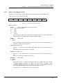
NOTICE
1.
The information contained herein can change without notice owing to product and/or technical
improvements. Before using the product, please make sure that the information being referred to is
up-to-date.
2.
The outline of action and examples for application circuits described herein have been chosen as an
explanation for the standard action and performance of the product. When planning to use the
product, please ensure that the external conditions are reflected in the actual circuit, assembly, and
program designs.
3.
When designing your product, please use our product below the specified maximum ratings and
within the specified operating ranges including, but not limited to, operating voltage, power
dissipation, and operating temperature.
4.
Oki assumes no responsibility or liability whatsoever for any failure or unusual or unexpected
operation resulting from misuse, neglect, improper installation, repair,
alteration or accident,
improper handling, or unusual physical or electrical stress including, but not limited to, exposure
to parameters beyond the specified maximum ratings or operation outside the specified operating
range.
5.
Neither indemnity against nor license of a third party's industrial and intellectual property right, etc.
is granted by us in connection with the use of product and/or the information and drawings
contained herein. No responsibility is assumed by us for any infringement of a third party’s right
which may result from the use thereof.
6.
The products listed in this document are intended for use in general electronics equipment for
commercial applications (e.g., office automation, communication equipment, measurement
equipment, consumer electronics, etc.). These products are not authorized for use in any system or
application that requires special or enhanced quality and reliability characteristics nor in any
system or application where the failure of such system or application may result in the loss or
damage of property, or death or injury to humans. Such applications include, but are not limited to,
traffic and automotive equipment, safety devices, aerospace equipment, nuclear power control,
medical equipment, and life-support systems.
7.
Certain products in this document may need governmental approval before they can be exported to
particular countries. The purchaser assumes the responsibility of determining the legality of export
of these products and will take appropriate and necessary steps at their own expense for these.
8.
No part of the contents contained herein may be reprinted or reproduced without our prior
permission.
9.
ARM, ARM POWERED logo and Thumb are registered trademarks of ARM Limited.
ARM7TDIM and Multi-ICE are trademarks of ARM Limited.
Copyright 2001 OKI ELECTRIC INDUSTRY CO., LTD.
Preface
The ML671000 is a 32-bit CMOS single-chip microcontroller combining a 32-bit ARM7TDMI RISC
CPU core developed by ARM Limited with a broad set of peripheral functions that make it ideal for
controlling PC peripherals, communications terminals, and the like.
This User’s Manual primarily covers the ML671000 hardware.
Application developers should also refer to the following related manuals and documents.
!
!
!
!
!
!
!
ARM7TDMI Data Sheet
ARM Software Development Toolkit User Guide
ARM Software Development Toolkit Reference Guide
Multi-ICE User Guide
OKI ADI-BOARD User’s Guide
ML671000 CPU BOARD User’s Guide
CAB_671000_P Board Kit Printer Interface Application Manual
(Sample program for USB device controller)
! USB Standard
- UNIVERSAL SERIAL BUS Specification Version 1.0
- UNIVERSAL SERIAL BUS Specification Version 1.1
This document is subject to change without notice.
Contents
Chapter 1
Overview
1.1. Features .................................................................................................................................1-2
1.2. Block Diagram ......................................................................................................................1-4
1.3. Pins........................................................................................................................................1-5
1.3.1. Pin Descriptions...............................................................................................................1-6
1.3.2. Pin Structure ..................................................................................................................1-11
1.3.3. Pin Treatment ................................................................................................................1-12
Chapter 2
CPU
2.1. Overview ...............................................................................................................................2-2
2.2. CPU Operating States............................................................................................................2-2
2.3. Switching State......................................................................................................................2-2
2.4. Memory Formats ...................................................................................................................2-2
2.5. Instruction Length .................................................................................................................2-3
2.6. Data Types ............................................................................................................................2-3
2.7. Operating Modes...................................................................................................................2-3
2.8. Registers................................................................................................................................2-4
2.8.1. The ARM state register set ..............................................................................................2-4
2.8.2. The Thumb state register set............................................................................................2-6
2.8.3. The relationship between ARM and Thumb state registers .............................................2-7
2.8.4. Accessing Hi registers in Thumb state.............................................................................2-7
2.9. The Program Status Registers ...............................................................................................2-8
2.9.1. The condition code flags..................................................................................................2-8
2.9.2. The control bits................................................................................................................2-8
2.10. Exceptions ...........................................................................................................................2-10
2.10.1. Action on entering an exception ....................................................................................2-10
2.10.2. Action on leaving an exception......................................................................................2-11
2.10.3. Exception entry/exit summary .......................................................................................2-11
2.10.4. FIQ.................................................................................................................................2-12
2.10.5. IRQ ................................................................................................................................2-12
2.10.6. Software interrupt ..........................................................................................................2-12
2.10.7. Undefined instruction ....................................................................................................2-12
2.10.8. Exception vectors ..........................................................................................................2-13
2.10.9. Exception priorities........................................................................................................2-13
2.11. Reset....................................................................................................................................2-14
Chapter 3
CPU Control Functions
3.1. Overview ...............................................................................................................................3-2
3.1.1. Pins ..................................................................................................................................3-3
3.1.2. Control Registers .............................................................................................................3-3
3.2. Detailed Control Register Descriptions.................................................................................3-4
3.2.1. Standby Control Register (SBYCON) .............................................................................3-4
3.2.2. Clock Control Register (CKCON)...................................................................................3-5
3.2.3. Clock Supply Wait Control Register (CKWTCON)........................................................3-6
3.2.4. Reset Status Register (RSTST)........................................................................................3-7
3.3. System Resets........................................................................................................................3-8
3.3.1. Resetting with External Input ..........................................................................................3-8
3.3.2. Resetting with Watchdog Timer Overflow ......................................................................3-8
3.4. System Clock (SYSCLK)......................................................................................................3-9
Contents-1
3.5. Standby Modes....................................................................................................................3-10
3.5.1. HALT Mode ..................................................................................................................3-10
3.5.2. STOP Mode...................................................................................................................3-11
3.6. Clock Supply Delay.............................................................................................................3-12
Chapter 4
Interrupt Controller
4.1. Overview ..................................................................................................................................4-2
4.1.1. Block Diagram ....................................................................................................................4-3
4.1.2. Pins......................................................................................................................................4-4
4.1.3. Control Registers.................................................................................................................4-4
4.2. Interrupt Sources ......................................................................................................................4-5
4.2.1. External FIQ Interrupt Requests..........................................................................................4-5
4.2.2. External Interrupt Requests.................................................................................................4-5
4.2.3. Internal Interrupt Requests ..................................................................................................4-5
4.2.4. Interrupt Sources, Interrupt Numbers, and Control Registers .............................................4-6
4.3. Detailed Control Register Descriptions ....................................................................................4-8
4.3.1. Interrupt Number Register (INR) ........................................................................................4-8
4.3.2. Current Interrupt Level Register (CILR).............................................................................4-8
4.3.3. Interrupt Request Level Register (IRLR) ............................................................................4-9
4.3.4. External FIQ Control Register (EFIQCON)........................................................................4-9
4.3.5. External Interrupt Control Register (EIRCON).................................................................4-10
4.3.6. Interrupt Request Registers (IRR0 and IRR1)...................................................................4-10
4.3.7. Interrupt Level Control Registers (ILCONn, n=0 to 5).....................................................4-11
4.4. Interrupt Processing................................................................................................................4-12
4.4.1. External FIQ Interrupts .....................................................................................................4-12
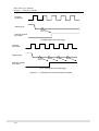
4.4.1.1. Interrupt Sequence ......................................................................................................4-12
4.4.2. External and Internal Interrupts.........................................................................................4-13
4.4.2.1. Interrupt Priority Levels..............................................................................................4-13
4.4.2.2. Interrupt Sequence ......................................................................................................4-14
4.4.2.3. Interrupt Level Control Example ................................................................................4-15
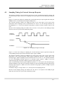
4.5. Sampling Timing for External Interrupt Requests..................................................................4-17
4.6. Interrupt Latency ....................................................................................................................4-19
4.7. Notes on Processing Interrupts...............................................................................................4-20
Chapter 5
I/O Ports
5.1. Overview ...............................................................................................................................5-2
5.1.1. Control Registers .............................................................................................................5-4
5.2. Detailed Control Register Descriptions.................................................................................5-5
5.2.1. Port Output Registers (POn, n=0 to 3).............................................................................5-5
5.2.2. Port Input Registers (PIn, n=0 to 3).................................................................................5-6
5.2.3. Port Mode Registers (PMn, n=0 to 3)..............................................................................5-7
5.2.4. Port Function Selection Registers (PFSn, n=0 to 3) ........................................................5-8
Chapter 6
Time Base Generator
6.1. Overview ...............................................................................................................................6-2
6.1.1. Block Diagram.................................................................................................................6-2
6.1.2. Control Registers .............................................................................................................6-3
6.2. Detailed Control Register Descriptions.................................................................................6-4
6.2.1. Watchdog Timer Control Register (WDTCON)..............................................................6-4
6.2.2. Time Base Control Register (TBGCON).........................................................................6-5
6.3. Time Base Generator Operation............................................................................................6-6
6.3.1. Time Base Counter (TBC)...............................................................................................6-6
Contents-2
6.3.2.
6.3.3.
6.3.4.
6.3.5.
Chapter 7
Watchdog Timer (WDT) .................................................................................................6-7
Watchdog Timer Overflow Interval (tWDT)...................................................................6-8
Watchdog Timer Operation .............................................................................................6-9
Interval Timer Operation ...............................................................................................6-11
Timers
7.1. Overview ...............................................................................................................................7-2
7.1.1. Block Diagram.................................................................................................................7-2
7.1.2. Pins ..................................................................................................................................7-4
7.1.3. Control Registers .............................................................................................................7-5
7.2. Detailed Control Register Descriptions.................................................................................7-6
7.2.1. Flexible Timer Control Registers (TMnCON, n=0 to 1) .................................................7-6
7.2.2. General-Purpose Timer Control Registers (TMnCON, n=2 to 3)....................................7-7
7.2.3. Flexible Timer Status Registers (TMnST, n=0 to 1) .......................................................7-8
7.2.4. General-Purpose Timer Status Registers (TMnST, n=2 to 3)..........................................7-8
7.2.5. Timer Counters (TMnC, n=0 to 3) ..................................................................................7-9
7.2.6. Timer Registers (TMnC, n=0 to 3) ..................................................................................7-9
7.2.7. Flexible Timer General-Purpose Registers (TMnGR, n=0 to 1)....................................7-10
7.2.8. Flexible Timer I/O Level Registers (TMnIOV, n=0 to 1) .............................................7-11
7.2.9. Flexible Timer Output Registers (TMnOUT, n=0 to 1).................................................7-12
7.2.10. Timer Enable Register (TMEN) ....................................................................................7-13
7.2.11. Timer Disable Register (TMDIS) ..................................................................................7-14
7.3. Timer Operation ..................................................................................................................7-15
7.3.1. Flexible Timer Operation ..............................................................................................7-15
7.3.1.1. Auto Reload Timer Mode ........................................................................................7-15
7.3.1.2. Compare Out Mode..................................................................................................7-16
7.3.1.3. Pulse Width Modulation (PWM) Mode...................................................................7-17
7.3.1.4. Capture Mode ..........................................................................................................7-18
7.3.2. General-Purpose Timer Operation.................................................................................7-18
7.3.3. Selecting Clock..............................................................................................................7-19
7.3.4. Starting/Stopping Timer ................................................................................................7-19
7.4. Timer I/O Timing ................................................................................................................7-20
7.4.1. Sampling External Clock Signal ....................................................................................7-20
7.4.2. Sampling Capture Trigger Input ....................................................................................7-21
7.4.3. Timer Output Timing.....................................................................................................7-22
Chapter 8
Universal Asynchronous Receiver/Transmitter (UART)
8.1. Overview ..................................................................................................................................8-2
8.1.1. Block Diagram ....................................................................................................................8-3
8.1.2. Pins......................................................................................................................................8-4
8.1.3. Control Registers.................................................................................................................8-5
8.2. Detailed Control Register Descriptions ....................................................................................8-6
8.2.1. UART Buffer Register (RBR/THR)....................................................................................8-6
8.2.2. UART Shift Registers (TSR and RSR) ...............................................................................8-6
8.2.3. FIFO Control Register (FCR) .............................................................................................8-7
8.2.4. Line Control Register (LCR)...............................................................................................8-8
8.2.5. Line Status Register (LSR)................................................................................................8-10
8.2.6. Modem Control Register (MCR) ......................................................................................8-13
8.2.7. Modem Status Register (MSR) .........................................................................................8-14
8.2.8. Scratch Pad Register (SCR) ..............................................................................................8-15
8.2.9. Interrupt Identification Register (IIR) ...............................................................................8-16
8.2.10. Interrupt Enable Register (IER) ......................................................................................8-18
8.2.11. Divisor Latch (DLL and DLM).......................................................................................8-19
Contents-3
8.2.12. Clock Select Register (CSR) ...........................................................................................8-20
8.3. Interrupts during Buffered Operation .....................................................................................8-21
8.3.1. Receive Interrupts .............................................................................................................8-21
8.3.2. Transmit Interrupts............................................................................................................8-23
8.4. Polled Operation.....................................................................................................................8-24
8.5. DMA Transfer Requests.........................................................................................................8-24
8.5.1. TXRDY.............................................................................................................................8-24
8.5.2. RXRDY.............................................................................................................................8-25
Chapter 9
Serial Communications Interface (SCI)
9.1. Overview ..................................................................................................................................9-2
9.1.1. Block Diagram ....................................................................................................................9-3
9.1.2. Pins......................................................................................................................................9-4
9.1.3. Control Registers.................................................................................................................9-4
9.2. Detailed Control Register Descriptions ....................................................................................9-5
9.2.1. SCI Transmit Control Register (STCON) ...........................................................................9-5
9.2.2. SCI Receive Control Register (SRCON) ............................................................................9-6
9.2.3. SCI Status Register (SCIST) ...............................................................................................9-7
9.2.4. SCI Buffer Register (SBUF) ...............................................................................................9-8
9.2.5. SCI Shift Registers ..............................................................................................................9-8
9.2.6. SCI Timer Counter (STMC) ...............................................................................................9-8
9.2.7. SCI Timer Register (STMR) ...............................................................................................9-9
9.2.8. SCI Timer Control Register (STMCON) ............................................................................9-9
9.3. Asynchronous (ASI) Operation ..............................................................................................9-10
9.3.1. Calculating Baud Rate.......................................................................................................9-10
9.3.2. Frame Formats ..................................................................................................................9-11
9.3.3. Transmitting Data..............................................................................................................9-12
9.3.4. Receiving Data ..................................................................................................................9-13
9.4. Clock Synchronous (CSI) Operation ......................................................................................9-14
9.4.1. Frame Formats ..................................................................................................................9-14
9.4.2. Transmitting Data..............................................................................................................9-14
9.4.2.1. Transmitting as Master ...............................................................................................9-15
9.4.2.2. Transmitting as Slave..................................................................................................9-16
9.4.3. Receiving Data ..................................................................................................................9-17
9.4.3.1. Receiving as Master....................................................................................................9-17
9.4.3.2. Receiving as Slave ......................................................................................................9-18
Chapter 10 Direct Memory Access Controller (DMAC)
10.1. Overview ..............................................................................................................................10-2
10.1.1. Block Diagram ................................................................................................................10-2
10.1.2. Pins..................................................................................................................................10-4
10.1.3. Control Registers.............................................................................................................10-5
10.2. Detailed Control Register Descriptions ................................................................................10-6
10.2.1. DMA Source Address Register 0 (DSAL0 and DSAH0)................................................10-6
10.2.2. DMA Destination Address Register 0 (DDAL0 and DDAH0) .......................................10-6
10.2.3. DMA Transfer Count Register 0 (DTC0) .......................................................................10-6
10.2.4. DMA Transfer Request Select Register 0 (DTRS0) .......................................................10-7
10.2.5. DMA Channel Mode Register 0 (DCM0) .......................................................................10-8
10.2.6. DMA Source Address Register 1 (DSAL1 and DSAH1)..............................................10-10
10.2.7. DMA Destination Address Register 1 (DDAL1 and DDAH1) .....................................10-10
10.2.8. DMA Transfer Count Register 1 (DTC1) .....................................................................10-10
10.2.9. DMA Transfer Request Select Register 1 (DTRS1) .....................................................10-11
10.2.10. DMA Channel Mode Register 1 (DCM1) ...................................................................10-12
Contents-4
10.2.11. DMA Command Register (DCMD) ............................................................................10-14
10.2.12. DMA End Status Register (DMAEST) .......................................................................10-15
10.2.13. DMA Status Register (DMAST) .................................................................................10-16
10.2.14. DMA Request Status Register (DREQST)..................................................................10-17
10.3. Operational Description .....................................................................................................10-18
10.3.1. Transfer Requests..........................................................................................................10-18
10.3.2. Addressing Mode ..........................................................................................................10-21
10.3.3. Transfer Modes .............................................................................................................10-23
10.3.4. Access Data Sizes .........................................................................................................10-25
10.3.5. Channel Priority Order ..................................................................................................10-25
10.3.6. DMA Transfer End Conditions .....................................................................................10-25
10.4. DMA Transfer Timing .......................................................................................................10-27
10.4.1. DMA Transfer Start Timing..........................................................................................10-27
10.4.2. Examples of DMA transfer timing ................................................................................10-28
10.5. Usage Notes........................................................................................................................10-32
Chapter 11 Universal Serial Bus Device Controller (USBC)
11.1. Overview .............................................................................................................................11-2
11.1.1. Block Diagram...............................................................................................................11-3
11.1.2. Pins ................................................................................................................................11-4
11.1.3. Control Registers ...........................................................................................................11-4
11.2. Detailed Control Register Descriptions...............................................................................11-6
11.2.1. Device Address Register (DVCADR) ...........................................................................11-6
11.2.2. Device Status Register (DVCSTAT) .............................................................................11-6
11.2.3. Packet Error Register (PKTERR)..................................................................................11-7
11.2.4. FIFO Status Registers (FIFOSTATn, n=1 to 2).............................................................11-8
11.2.5. Frame Number Register Pair (FRAMEMSB and FRAMELSB) ...................................11-9
11.2.6. Endpoint Packet Ready Register (PKTRDY) ..............................................................11-10
11.2.7. Endpoint 0 Receive Byte Count Register (EP0RXCNT).............................................11-12
11.2.8. Endpoint 1 Receive Byte Count Register (EP1RXCNT).............................................11-12
11.2.9. Endpoint 2 Receive Byte Count Register (EP2RXCNT).............................................11-13
11.2.10. Endpoint 3 Receive Byte Count Register Pair
(EP3RXCNTMSB and EP3RXCNTLSB)...................................................................11-14
11.2.11. Transmit FIFO Buffer Clear Register (CLRFIFO) ......................................................11-15
11.2.12. Software Reset Register (SOFTRST) ..........................................................................11-15
11.2.13. Request Setup Registers...............................................................................................11-16
11.2.14. Interrupt Enable Registers (INTENBLn, n=1 to 2) .....................................................11-18
11.2.15. Interrupt Status Registers (INTSTATn, n=1 to 2) .......................................................11-19
11.2.16. Endpoint 2 DMA Control Register (DMACON2).......................................................11-22
11.2.17. Endpoint 2 DMA Interval Register (DMAINTVL2) ...................................................11-22
11.2.18. Endpoint 3 DMA Control Register (DMACON3).......................................................11-23
11.2.19. Endpoint 3 DMA Interval Register (DMAINTVL3) ...................................................11-24
11.2.20. Endpoint 0 Receive Control Register (EP0RXCON) ..................................................11-24
11.2.21. Endpoint 0 Receive Data Toggle Register (EP0RXTGL) ...........................................11-25
11.2.22. Endpoint 0 Receive Payload Register (EP0RXPLD) ..................................................11-25
11.2.23. Endpoint 1 Control Register (EP1CON) .....................................................................11-26
11.2.24. Endpoint 1 Data Toggle Register (EP1TGL) ..............................................................11-27
11.2.25. Endpoint 1 Payload Register (EP1PLD)......................................................................11-27
11.2.26. Endpoint 0 Transmit Control Register (EP0TXCON) .................................................11-28
11.2.27. Endpoint 0 Transmit Data Toggle Register (EP0TXTGL) ..........................................11-28
11.2.28. Endpoint 0 Transmit Payload Register (EP0TXPLD) .................................................11-29
11.2.29. Endpoint 0 Status Register (EP0STAT) ......................................................................11-29
11.2.30. Endpoint 2 Control Register (EP2CON) .....................................................................11-30
11.2.31. Endpoint 2 Data Toggle Register (EP2TGL) ..............................................................11-31
Contents-5
11.2.32. Endpoint 2 Payload Register (EP2PLD)......................................................................11-31
11.2.33. EP3 Endpoint 3 Control Register (EP3CON)..............................................................11-32
11.2.34. Endpoint 3 Data Toggle Register (EP3TGL) ..............................................................11-33
11.2.35. Endpoint 3 Payload Register Pair (EP3PLDLSB and EP3PLDMSB).........................11-33
11.2.36. Endpoint 0 FIFO Buffer Register (EP0RXFIFO/EP0TXFIFO) ..................................11-34
11.2.37. Endpoint 1 FIFO Buffer Register (EP1RXFIFO/EP1TXFIFO) ..................................11-34
11.2.38. Endpoint 2 FIFO Buffer Register (EP2RXFIFO/EP2TXFIFO) ..................................11-34
11.2.39. Endpoint 3 FIFO Buffer Register (EP3RXFIFO/EP3TXFIFO) ..................................11-35
11.2.40. Wake-up Control Register (AWKCON)......................................................................11-35
11.3. Paired FIFO buffers Operation..........................................................................................11-36
11.3.1. Bulk (Interrupt) Transfers............................................................................................11-36
11.3.2. Isochronous Transfers..................................................................................................11-37
11.4. DMA Transfer Control......................................................................................................11-39
11.4.1. Transfer Request Conditions .......................................................................................11-39
11.4.2. Transfer Request Timing .............................................................................................11-40
11.5. Power Conservation Function ...........................................................................................11-41
11.6. Usage Notes ......................................................................................................................11-42
Chapter 12 External Memory Controller (XMC)
12.1. Overview .............................................................................................................................12-2
12.1.1. Block Diagram...............................................................................................................12-3
12.1.2. Pins ................................................................................................................................12-5
12.1.3. Control Registers ...........................................................................................................12-6
12.1.4. Address Space ...............................................................................................................12-7
12.2. Detailed Control Register Descriptions...............................................................................12-9
12.2.1. Bus Width Control Register (BWCON) ........................................................................12-9
12.2.2. WAIT Input Control Register (WICON).....................................................................12-10
12.2.3. Off Time Control Register (OTCON)..........................................................................12-11
12.2.4. Programmable Wait Control Register (PWCON)........................................................12-12
12.2.5. Bus Access Control Register (BACON) ......................................................................12-13
12.2.6. DRAM Bank 2 Control Register (DR2CON) ..............................................................12-14
12.2.7. DRAM Bank 3 Control Register (DR3CON) ..............................................................12-15
12.2.8. DRAM Bank 2 Access Timing Control Register (AT2CON)......................................12-16
12.2.9. DRAM Bank 3 Access Timing Control Register (AT3CON)......................................12-16
12.2.10. DRAM Bank 2 Programmable Wait Control Register (DW2CON) ............................12-17
12.2.11. DRAM Bank 3 Programmable Wait Control Register (DW3CON) ............................12-17
12.2.12. Refresh Timer Counter (RFTCN)................................................................................12-18
12.2.13. Refresh Cycle Control Register (RCCON) ..................................................................12-18
12.2.14. Refresh Timing Control Register (RTCON)................................................................12-19
12.2.15. Refresh Control Register (RFCON).............................................................................12-20
12.3. Accessing Address Space ..................................................................................................12-22
12.3.1. Data Bus Width ...........................................................................................................12-22
12.3.2. Accessing Bank 0/1 External Memory Space ..............................................................12-23
12.3.2.1. Basic Access ..........................................................................................................12-23
12.3.2.2. Wait Cycles............................................................................................................12-24
12.3.2.3. Half-Word Access..................................................................................................12-25
12.3.3. Accessing Bank 2/3 External Memory (DRAM) Space ..............................................12-26
12.3.3.1. Address Multiplexing.............................................................................................12-26
12.3.3.2. Basic Access ..........................................................................................................12-27
12.3.3.3. Wait Cycles............................................................................................................12-28
12.3.3.4. Half-Word Access..................................................................................................12-32
12.3.3.5. Fast page (Burst) Access.....................................................................................12-33
12.3.3.6. Refresh Access.......................................................................................................12-33
Contents-6
12.3.4. External Memory Space Access for All Banks............................................................12-37
12.3.4.1. Off Time Control ...................................................................................................12-37
12.3.4.2. Store Buffer............................................................................................................12-38
12.3.5. Accessing Bank 0 Internal Memory Space ..................................................................12-39
12.4. Bus Arbitration..................................................................................................................12-40
12.4.1. Bus Access Priority......................................................................................................12-40
12.4.2. Requesting and obtaining Access to External Bus..................................................... -12-40
12.4.3. Bus Lock Operation.....................................................................................................12-42
12.5. Standby Modes..................................................................................................................12-43
12.5.1. Shifting to HALT Mode ..............................................................................................12-43
12.5.2. Shifting to STOP Mode ...............................................................................................12-43
12.6. Connecting External Memory ...........................................................................................12-44
12.6.1. Connecting ROM.........................................................................................................12-44
12.6.2. Connecting SRAM.......................................................................................................12-46
12.6.3. Connecting DRAM ......................................................................................................12-48
Chapter 13 Electrical Characteristics
13.1. Absolute Maximum Ratings .................................................................................................13-2
13.2. Recommended Operating Conditions...................................................................................13-2
13.3. DC Characteristics................................................................................................................13-3
13.4. AC Characteristics................................................................................................................13-4
13.4.1. Clock Timing ..................................................................................................................13-4
13.4.2. Control Signal Timing.....................................................................................................13-4
13.4.3. External Bus Timing .......................................................................................................13-5
13.5. Timing Diagram ...................................................................................................................13-6
13.5.1. Clock Timing ..................................................................................................................13-6
13.5.2. Control Signal Timing.....................................................................................................13-7
13.5.3. DMA Timing...................................................................................................................13-8
13.5.4. nXWAIT Signal Input Timing ........................................................................................13-8
13.5.5. External Bus Release Timing ..........................................................................................13-9
13.5.6. Bank 0, 1 Write Cycle...................................................................................................13-10
13.5.7. Bank 0, 1 Read Cycle....................................................................................................13-11
13.5.8. Bank 2, 3 Write Cycle...................................................................................................13-12
13.5.9. Bank 2, 3 Read Cycle....................................................................................................13-13
13.5.10. CAS Before RAS (CBR) Refresh................................................................................13-13
13.5.11. Self-Refresh.................................................................................................................13-14
Appendix
A. List of Control Registers........................................................................................................... A-2
B. Sample Circuits......................................................................................................................... A-8
B.1. Crystal Oscillation circuit..................................................................................................... A-8
B.2. USB Interface Circuit........................................................................................................... A-9
B.3. JTAG Interface Circuit....................................................................................................... A-10
C. Package Dimensions............................................................................................................... A-11
Contents-7
Chapter 1
Overview
1-1
ML671000 User’s Manual
Chapter 1 Overview
1.1.
Features
This high-performance 32-bit single-chip microcontroller combines a 32-bit ARM7TDMI RISC
CPU core developed by ARM Limited with such peripheral functions as USB device controller,
DMA controller (DMAC), universal asynchronous receiver transmitter (UART), serial
communications interface, and 16-bit timers. It therefore offers a highly optimized combination of
32-bit data processing capabilities, built-in memory, and on-chip peripherals for controlling PC
peripherals and communications devices. A built-in external memory controller (XMC) supports
direct connection to memory—SRAM and DRAM, for example—and peripheral devices for adding
even more functionality.
The following is a list of features.
!
!
CPU
•
32-bit RISC CPU core (ARM7TDMI)
•
Two instruction sets: Rich set of 32-bit ARM instructions and a subset, the 16-bit Thumb
instructions, offering higher code efficiency.
•
29 32-bit general-purpose registers
•
Built-in multiplication unit
Internal Memory
•
!
I/O Ports
•
!
!
•
Two flexible 16-bit timers offering a choice of four operation modes: auto reload timer
(ART), compare out (CMO), pulse width modulation (PWM), or capture input (CAP)
•
Two general-purpose 16-bit auto reload timers
Universal Asynchronous Receiver/Transmitter (UART)
Functionally equivalent to the 16550A, this block includes 16-byte FIFO buffers for both
transmit and receive and a built-in baud rate generator.
Serial Communications Interface (SCI)
•
!
64 individually configurable, bidirectional I/O pins
Timers
•
!
4 kilobytes of RAM
This supports two communications modes: asynchronous (UART) and clock synchronous.
It includes a built-in baud rate generator.
USB Device Controller (USBC)
•
Full-speed (12 Mbps) operation compliant with USB 1.1.
•
Transfer types: Control, bulk, isochronous, and interrupt
•
Four bidirectional endpoints with the following buffers
Endpoint 0 64 bytes each for transmit and receive
Endpoint 1 64 bytes×1 (bidirectional)
Endpoint 2 64 bytes×2 (bidirectional, alternating)
Endpoint 3 256 bytes×2 (bidirectional, alternating)
1-2
ML671000 User’s Manual
Chapter 1 Overview
!
!
DMA Controller (DMAC)
•
Two channels
•
Single and dual addressing
•
Cycle steal and burst transfers
•
8- and 16-bit data transfers
•
Maximum number of data items per transfer: 65,536
•
Addressing space: 64 megabytes
Interrupt Controller
•
Maximum of 22 interrupt sources
One external fast interrupt request (FIQ)
Eight external interrupts
Thirteen internal interrupts
•
!
!
!
!
External Memory Controller (XMC)
•
Direct connection of ROM, SRAM, DRAM, and external peripheral devices
•
Memory control for four banks: Two for ROM, RAM, or peripheral devices; two for
DRAM
•
Separate wait control and other parameters for each bank
•
Bus arbitration
Clock generator
•
Built-in crystal oscillator circuit
•
Built-in ×4 phase-locked loop (PLL) allowing a single 12-MHz crystal oscillator to supply
both a 48-MHz clock signal to the USB device controller and a 24-MHz (max.) one to the
CPU and the built-in peripheral devices Clock gear shifting for switching operating clock
frequency with processing load over fourfold range: ×1/2, ×1, ×2
Time Base Generator (TBG)
•
Time base clock supplies for built-in peripheral devices
•
12-bit watchdog timer
Standby Functions
•
!
HALT and STOP modes
Onboard debugging function
•
!
Interrupt sources are assigned one of eight priority levels.
JTAG interface allowing onboard debugging
Package:
128 pin QFP
1-3
ML671000 User’s Manual
Chapter 1 Overview
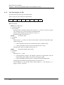
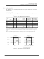
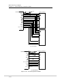
Block Diagram
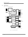
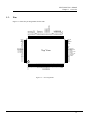
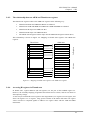
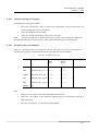
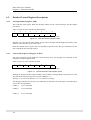
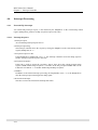
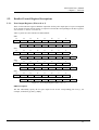
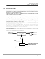
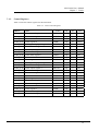
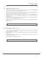
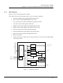
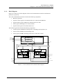
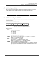
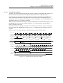
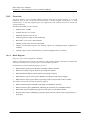
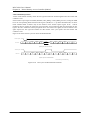
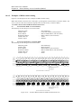
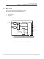
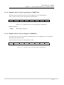
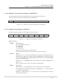
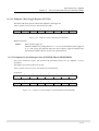
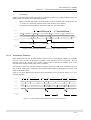
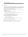
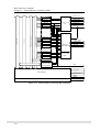
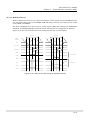
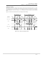
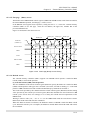
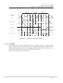
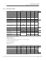
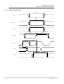
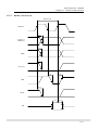
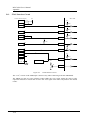
Figure 1-1 gives a block diagram for this LSI.
nRST
nEA
DBSEL
TEST
TMS
nTRST
TDI
TCK
TDO
ARM7DTMI
P0[7:0]/XA[23:16]
XA[15:1]
RAM
XA0/nLB
XD[15:0]
nR/W
nCS0
nRD
nWRE/nWRL
P1.7/nXWAIT
P1.6/nCS1
P1.5/nHB/nWRH
P1.4/nRAS1
P1.3/nWH/nCASH
P1.2/nRAS0
P1.1/nCAS/nCASL
P1.0/nWL/nWE
32-bit Core Address Bus
VDD
VSS
32-bit Core Address Bus
Bus Controller for Internal Bus and
External Memory
P6.7/nBACK
P6.6/nBREQ
nEFIQ
2-channel
DMAC
Interrupt Controller
P5.7/ DTR
P5.6/ RTS
P5.5/ CTS
P5.4/ DSR
P5.3/ DCD
P5.2/ RI
P5.1/OUT1
P5.0/OUT2
P4.7/SOUT
P4.6/ SIN
UART Port
(16550A compatible)
P4.5/TXD0
P4.4/RXD0
P4.3/ TXC
P4.2/ RXC
Serial
Communications
Interface
P2[7:0]/EIR[7:0]
Peripheral Address Bus
(16 bits)
Time Base Generator
Flexible & GeneralPurpose Auto Reload
Timer
(two each)
Peripheral Data Bus
P6.5/nDACK1
P6.4/nDACK0
P6.3/nDREQ1
P6.2/nDREQ0
P3.7/TMCLK3
P3.6/TMCLK2
P3.5/TMCLK1
P3.4/TMCLK0
P3.3/TMIN3/TMOUT3
P3.2/TMIN2/TMOUT2
D+
USBC
D-
PLL
I/O Ports
OSC0
OSC1
CLKOUT
PLLEN
P0[7:0]*
P1[7:0]*
P2[7:0]*
P3[7:0]*
P4[7:0]*
P5[7:0]*
P7[7:0]
OSCVDD
OSCVSS
P6[7:0]*
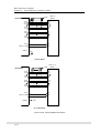
1.2.
Asterisks indicate pins with secondary functions.
Figure 1-1 ML671000 Block Diagram
1-4
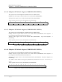
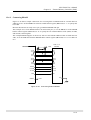
nEFIQ
nRST
nTRST
TDO
TDI
TMS
TCK
TEST
P6.0
P6.1
P6.2/nDREQ0
P6.3/nDREQ1
P6.4/DACK0
P6.5/DACK1
P6.6/nBREQ
P6.7/nBACK
VSS
VDD
P7.0
P7.1
P7.2
P7.3
P7.4
P7.5
P7.6
P7.7
103
104
105
106
107
108
109
110
111
112
113
114
115
116
117
118
119
120
121
122
123
124
125
126
127
128
1
2
3
4
5
6
7
8
9
10
11
12
13
14
15
16
17
18
19
20
21
22
23
24
25
26
27
28
29
30
31
32
33
34
35
36
37
38
102
101
100
99
98
97
96
95
94
93
92
91
90
89
88
87
86
85
84
83
82
81
80
79
78
77
76
75
74
73
72
71
70
69
68
67
66
65
P5.7/DTR
P5.6/RTS
P5.5/CTS
P5.4/DSR
P5.3/DCD
P5.2/RI
P5.1/OUT2
P5.0/OUT1
VDD
VSS
P4.7/SOUT
P4.6/SIN
P4.5/TXD
P4.4/RXD
P4.3/TXC
P4.2/RXC
P4.1
P4.0
P3.7/TMCLK3
P3.6/TMCLK2
P3.5/TMCLK1
P3.4/TMCLK0
P3.3/TMIN1/TMOUT1
P3.2/TMIN0/TMOUT0
P3.1
P3.0
VDD
VSS
P2.7/nEIR7
P2.6/nEIR6
P2.5/nEIR5
P2.4/nEIR4
P2.3/nEIR3
P2.2/nEIR2
P2.1/nEIR1
P2.0/nEIR0
PLLEN
CLKOUT
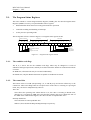
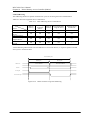
1.3.
XA0/nLB
XA1
XA2
XA3
XA4
XA5
XA6
XA7
XA8
XA9
XA10
XA11
XA12
XA13
XA14
XA15
P0.0/XA16
P0.1/XA17
P0.2/XA18
P0.3/XA19
P0.4/XA20
P0.5/XA21
P0.6/XA22
P0.7/XA23
VSS
VDD
XD0
XD1
XD2
XD3
XD4
XD5
XD6
XD7
XD8
XD9
XD10
XD11
ML671000 User’s Manual
Chapter 1 Overview
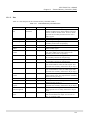
Pins
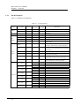
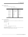
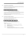
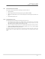
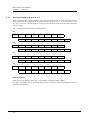
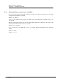
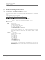
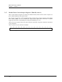
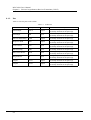
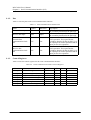
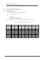
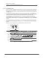
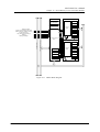
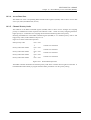
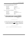
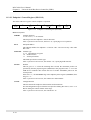
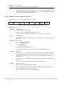
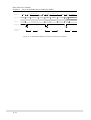
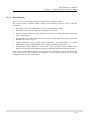
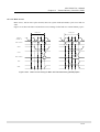
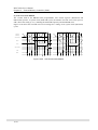
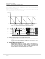
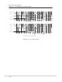
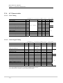
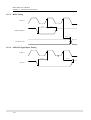
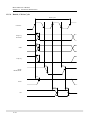
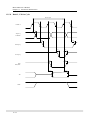
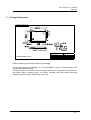
Figure 1-2 shows the pin assignments for this LSI.
Top View
64
63
62
61
60
59
58
57
56
55
54
53
52
51
50
49
48
47
46
45
44
43
42
41
40
39
OSCVSS
OSC1
OSC0
OSCVDD
nEA
DBSEL
DD+
VDD
VSS
P1.7/nXWAIT
P1.6/nCS1
P1.5/nHB/nWRH
P1.4/nRAS1
P1.3/nWH/nCASH
P1.2/nRAS0
P1.1/nCAS/nCASL
P1.0/nWL/nWE
nWRE/nWRL
nRD
nCS0
nR/W
XD15
XD14
XD13
XD12
Figure 1-2 Pin Assignments
1-5
ML671000 User’s Manual
Chapter 1 Overview
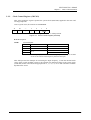
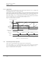
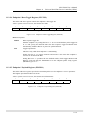
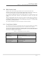
1.3.1.
Pin Descriptions
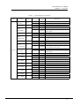
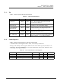
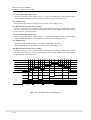
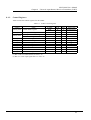
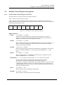
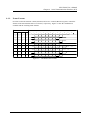
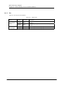
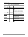
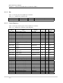
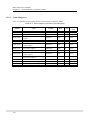
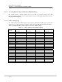
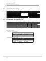
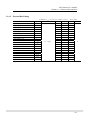
Table 1-1 summarizes pin functions.
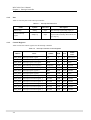
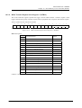
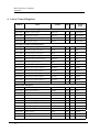
Table 1-1 Pin Descriptions
Type
Address
bus
Data bus
Bus
control
Pin Name
Number
I/O
Direction
Primary/
secondary
XA15 to XA1
nLB/XA0
16 to 2
1
O
O
-
XD15 to XD0
nCS0
nRD
nR/W
nWRE/nWRL
42 to 26
44
45
43
46
I/O
O
O
O
-
OSC0
62
I
OSC1
63
O
CLKOUT
PLLEN
65
66
O
I
-
OSCVDD
61
I
-
OSCVSS
64
I
-
P0.7 / XA23
24
P0.6 / XA22
23
P0.5 / XA21
22
P0.4 / XA20
21
P0.3 / XA19
20
P0.2 / XA18
19
P0.1 / XA17
18
P0.0 / XA16
17
I/O
O
I/O
O
I/O
O
I/O
O
I/O
O
I/O
O
I/O
O
I/O
O
Primary
Secondary
Primary
Secondary
Primary
Secondary
Primary
Secondary
Primary
Secondary
Primary
Secondary
Primary
Secondary
Primary
Secondary
O
-
Clock
control
I/O ports
1-6
Description
External address bus bits 15 to 1
Bank 0/1 lower byte select or external address
bus bit 0
External data bus (XD)
Bank 0 chip select signal
Bank 0/1 read signal
Read strobe signal
Bank 0/1 write enable or lower byte write
enable signal
Connection pin for crystal oscillator or ceramic
resonator. Alternatively, external clock input.
Connection pin for crystal oscillator or ceramic
resonator. Leave open when using an external
clock supply.
Internal system clock output
Built-in PLL enable pin. Input “H” level when
using phase-locked loop.
Power supply for oscillation circuit and phaselocked loop. Connect to the power supply.
Ground for internal oscillation circuit and
phase-locked loop. Connect to ground.
Port 0 bit 7
External address bus bit 23
Port 0 bit 6
External address bus bit 22
Port 0 bit 5
External address bus bit 21
Port 0 bit 4
External address bus bit 20
Port 0 bit 3
External address bus bit 19
Port 0 bit 2
External address bus bit 18
Port 0 bit 1
External address bus bit 17
Port 0 bit 0
External address bus bit 16
ML671000 User’s Manual
Chapter 1 Overview
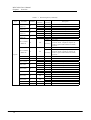
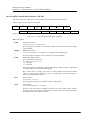
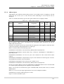
Table 1-1 Pin Descriptions (continued)
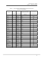
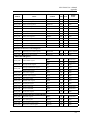
Type
I/O ports
Pin Name
Number
P1.7 /
nXWAIT
54
P1.6 / nCS1
53
P1.5 /
nHB/nWRH
52
P1.4 / nRAS1
51
P1.3 /
nWH/nCASH
50
P1.2 / nRAS0
49
P1.1/
nCAS/nCASL
48
P1.0 /
nWL/nWE
47
P2.7 / nEIR7
74
P2.6 / nEIR6
73
P2.5 / nEIR5
72
P2.4 / nEIR4
71
P2.3 / nEIR3
70
P2.2 / nEIR2
69
P2.1 / nEIR1
68
P2.0 / nEIR0
67
I/O
Direction
Primary/
secondary
I/O
I
I/O
O
I/O
Primary
Secondary
Primary
Secondary
Primary
O
Secondary
I/O
O
I/O
O
Primary
Secondary
Primary
Secondary
I/O
O
I/O
Primary
Secondary
Primary
O
Secondary
I/O
Primary
O
Secondary
I/O
I
I/O
I
I/O
I
I/O
I
I/O
I
I/O
I
I/O
I
I/O
I
Primary
Secondary
Primary
Secondary
Primary
Secondary
Primary
Secondary
Primary
Secondary
Primary
Secondary
Primary
Secondary
Primary
Secondary
Description
Port 1 bit 7
External wait cycle extension
Port 1 bit 6
Bank 1 chip select signal
Port 1 bit 5
Bank 0/1 upper byte select or upper byte write
enable signal
Port 1 bit 4
Bank 3 row address strobe signal
Port 1 bit 3
Bank 2/3 upper byte column address strobe
signal
Port 1 bit 2
Bank 2 row address strobe signal
Port 1 bit 1
Bank 2/3 column address strobe or lower byte
column address strobe signal
Port 1 bit 0
Bank 2/3 lower byte write enable or write
enable signal
Port 2 bit 7
External interrupt 7 input pin
Port 2 bit 6
External interrupt 6 input pin
Port 2 bit 5
External interrupt 5 input pin
Port 2 bit 4
External interrupt 4 input pin
Port 2 bit 3
External interrupt 3 input pin
Port 2 bit 2
External interrupt 2 input pin
Port 2 bit 1
External interrupt 1 input pin
Port 2 bit 0
External interrupt 0 input pin
1-7
ML671000 User’s Manual
Chapter 1 Overview
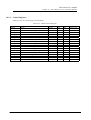
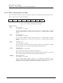
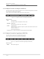
Table 1-1 Pin Descriptions (continued)
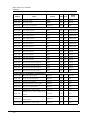
Type
Pin Name
P3.7 /
TMCLK3
P3.6 /
TMCLK2
P3.5 /
TMCLK1
P3.4 /
TMCLK0
P3.3 / TMIN1
/ TMOUT1
Number
84
83
82
81
80
I/O
Direction
Primary/
secondary
I/O
I
I/O
I
I/O
I
I/O
I
Primary
Secondary
Primary
Secondary
Primary
Secondary
Primary
Secondary
Primary
I/O
Secondary
Primary
P3.2 / TMIN0
/ TMOUT0
79
I/O
P3.1
P3.0
78
77
P4.7 / SOUT
92
P4.6 / SIN
91
P4.5 / TXD
90
P4.4 / RXD
89
I/O
I/O
I/O
O
I/O
I
I/O
O
I/O
I
P4.3 / TXC
88
I/O
P4.2 / RXC
87
I/O
P4.1
P4.0
86
85
I/O
I/O
Secondary
I/O ports
1-8
Primary
Secondary
Primary
Secondary
Primary
Secondary
Primary
Secondary
Primary
Secondary
Primary
Secondary
-
Description
Port 3 bit 7
Timer 3 external clock input
Port 3 bit 6
Timer 2 external clock input
Port 3 bit 5
Timer 1 external clock input
Port 3 bit 4
Timer 0 external clock input
Port 3 bit 3
Timer 1 input for capture input (CAP)
operation; Timer 1 output for compare out
(CMO) or pulse width modulation (PWM)
operation
Port 3 bit 2
Timer 0 input for capture input (CAP)
operation; Timer 0 output for compare out
(CMO) or pulse width modulation (PWM)
operation
Port 3 bit 1
Port 3 bit 0
Port 4 bit 7
UART serial data output
Port 4 bit 6
UART serial data input
Port 4 bit 5
SCI transmit data output
Port 4 bit 4
SCI receive data input
Port 4 bit 3
SCI transmit clock I/O
Port 4 bit 2
SCI receive clock I/O
Port 4 bit 1
Port 4 bit 0
ML671000 User’s Manual
Chapter 1 Overview
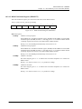
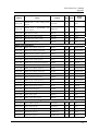
Table 1-1 Pin Descriptions (continued)
Type
Pin Name
P5.7 / DTR
I/O ports
Number
Primary/
secondary
I/O
Primary
O
I/O
O
I/O
I
I/O
I
I/O
I
I/O
I
I/O
O
I/O
O
I/O
O
I/O
I
I/O
O
I/O
O
I/O
I
I/O
I
I/O
I/O
I/O
I/O
I/O
I/O
I/O
I/O
I/O
I/O
Secondary
Primary
Secondary
Primary
Secondary
Primary
Secondary
Primary
Secondary
Primary
Secondary
Primary
Secondary
Primary
Secondary
Primary
Secondary
Primary
Secondary
Primary
Secondary
Primary
Secondary
Primary
Secondary
Primary
Secondary
-
Description
Port 5 bit 7
102
P5.6 / RTS
101
P5.5 / CTS
100
P5.4 / DSR
99
P5.3 / DCD
98
P5.2 / RI
97
P5.1 / OUT1
96
P5.0 / OUT2
95
P6.7 / nBACK
118
P6.6 / nBREQ
117
P6.5 / DACK1
116
P6.4 / DACK0
115
P6.3 /
nDREQ1
P6.2 /
nDREQ0
P6.1
P6.0
P7.7
P7.6
P7.5
P7.4
P7.3
P7.2
P7.1
P7.0
I/O
Direction
114
113
112
111
128
127
126
125
124
123
122
121
UART DTR signal output
Port 5 bit 6
UART RTS signal output
Port 5 bit 5
UART CTS signal
Port 5 bit 4
UART DSR signal
Port 5 bit 3
UART DCD signal
Port 5 bit 2
UART RI signal input pin
Port 5 bit 1
UART OUT1 signal output
Port 5 bit 0
UART OUT2 signal output
Port 6 bit 7
Bus release request accept signal output
Port 6 bit 6
Bus release request signal
Port 6 bit 5
Data transfer request 1 accept signal output
Port 6 bit 4
Data transfer request 0 accept signal output
Port 6 bit 3
Data transfer request 1 signal
Port 6 bit 2
Data transfer request 0 signal
Port 6 bit 1
Port 6 bit 0
Port 7 bit 7
Port 7 bit 6
Port 7 bit 5
Port 7 bit 4
Port 7 bit 3
Port 7 bit 2
Port 7 bit 1
Port 7 bit 0
1-9
ML671000 User’s Manual
Chapter 1 Overview
Table 1-1 Pin Descriptions (continued)
Type
USB port
Debugging
interface
Interrupts
System
control
Pin Name
I/O
Direction
Primary/
secondary
Description
D+
DTCK
TMS
TDI
TDO
nTRST
nEFIQ
nEA
nRST
57
58
109
108
107
106
105
103
60
104
I/O
I/O
I
I
I
O
I
I
I
I
-
DBSEL
59
I
-
I
-
TEST
110
I
-
Power supply pins. Connect all VDD pins to
the power supply.
I
-
Power supply ground pins. Connect all VSS
pins to ground.
VDD
Power
supply
VSS
1-10
Number
26,56,
76,94,
120
25,55,
75,93,
119
USB data I/O
Test clock input
Test mode select input
Test data input
Test data output
Boundary scan logic reset input
External fast interrupt request (FIQ) input
Connect this pin to ground.
LSI system reset signal input
Bank 0 data bus width select, read only during a
system reset. Input “H” level for 16 bits; “L”
level for 8 bits.
Test and debugging mode select input.
Normally connect to ground. Input “H” level
when using debugging mode.
ML671000 User’s Manual
Chapter 1 Overview
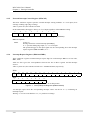
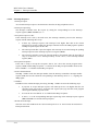
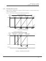
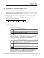
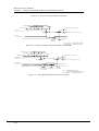
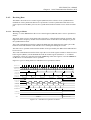
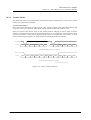
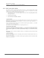
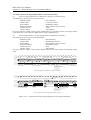
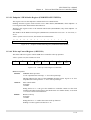
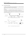
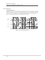
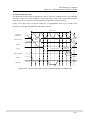
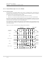
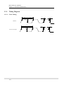
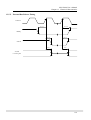
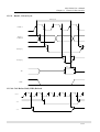
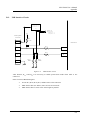
Pin Structure
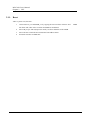
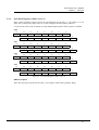
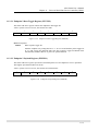
Figure 1-3 shows the structures of the I/O pins.
Pin names:
TDI,TMS,
TCK,
(2) nRST
Pin names:
P7[7:0],P6[7:0],
P6[7:0],P5[7:0],
P4[7:0],P3[7:0],
P2[7:0],P1[7:0],
(1)
P0[7:0]
5-V tolerant
VDD
50KΩ
Input
Control
I
O
Output
Enable
Input/output pins
Input pins
Pin names:
PLLEN,
DBSEL,
(1) nEA,
nEFIQ,
TEST
5-V tolerant; CMOS level inputs
Pin names:
XD[15:0]
Input
Control
I
Pin names:
nTRST
(2)
O
(3)
50KΩ
Output
Enable
5-V tolerant, TTL level inputs
Output pins
1.3.2.
Pin names:
XA0/nLB,
XA[15:1],
nR/W,nCS0,nRD
nWRE/nWRL,
CLKOUT,TDO
Figure 1-3 Pin Structures
1-11
ML671000 User’s Manual
Chapter 1 Overview
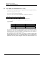
1.3.3.
Pin Treatment
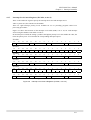
Table 1-2 gives pin treatments when pins are not used.
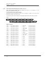
Table 1-2 Pin Treatments
Pin name
In use
Not in use
-
“H” or “L” level for input.
P7[7:0] to P0[7:0]
Leave open for output.
nEFIQ
-
Input “H” level.
nEA
Always connect to ground.
XD[15:8]
-
Leave open.
D+
-
Connect with 1.5kΩ pull-up.
D-
-
Connect to ground.
JTAG operation requires a pull-up resistor
Leave open.
of approximately 5.1 kΩ. (Note that this
nTRST
resistor is not necessary with Oki in-circuit
emulators.)
TDI,TMS,TCK,TDO
-
Leave open.
Input “H” level when debugging with the
Connect to ground.
TEST
JTAG interface.
1-12
Chapter 2
CPU
2-1
ML67100 User’s Manual
Chapter 2 CPU
2.1.
Overview
This LSI uses as its CPU the ARM7TDMI core developed by ARM Limited. This CPU offers the
programmer a choice of two states: ARM state, executing 32-bit ARM instructions, and Thumb
state, executing 16-bit Thumb instructions, a subset of ARM instructions.
2.2.
CPU Operating States
From the programmer's point of view, the CPU can be in one of two states:
ARM state
which executes 32-bit, word-aligned ARM instructions.
Thumb state
which operates with 16-bit, halfword-aligned Thumb instructions.
In this state, the PC uses bit 1 to select between alternate halfwords.
Note:
2.3.
Transition between these two states does not affect the CPU mode or the contents of
the registers.
Switching State
Entering Thumb state
Entry into Thumb state can be achieved by executing a BX instruction with the state bit (bit0)
set in the operand register.
Transition to Thumb state will also occur automatically on return from an exception (IRQ, FIQ,
UNDEF, SWI etc.), if the exception was entered with the processor in Thumb state.
Entering ARM state
Entry into ARM state happens:
2.4.
•
On execution of the BX instruction with the state bit clear in the operand register.
•
On the processor taking an exception (IRQ, FIQ, RESET, UNDEF, SWI etc.).
In this case, the PC is placed in the exception mode's link register, and execution
commences at the exception's vector address.
Memory Formats
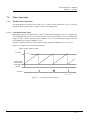
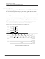
The CPU views memory as a linear collection of bytes numbered upwards from zero.
Bytes 0 to 3 hold the first stored word, bytes 4 to 7 the second and so on. The CPU can treat
words in memory as being stored in Little Endian format.
Note:
2-2
The core architecture supports both big- and little- endian formats, but this LSI uses
only the latter.
ML671000 User’s Manual
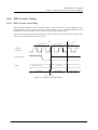
Chapter 2 CPU
Higher Address
31
11
7
3
24
23
10
6
2
16
15
9
5
1
8
7
8
4
0
0
Word Address
8
4
0
Lower Address
-Least significant byte is at lowest address
-Word is addressed by byte address of least significant byte
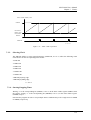
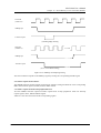
Figure 2-1
2.5.
Little endian addresses of bytes within words
Instruction Length
Instructions are either 32 bits long (in ARM state) or 16 bit long (in Thumb state).
2.6.
Data Types
The CPU supports byte (8-bit), halfword (16-bit) and word (32-bit) data types.
Words must be aligned to four-byte boundaries and half words to two-byte boundaries.
2.7.
Operating Modes
The CPU supports six modes of operation:
User (usr):
The normal ARM program execution state
FIQ(fiq): Designed to support a data transfer or channel process
IRQ(irq): Used for general-purpose interrupt handling
Supervisor (svc):
Protected mode for the operating system.
System (sys):
A privileged user mode for the operating system
Undefined(und):
Entered when an undefined instruction is executed
Note:
it.
The core architecture offers an additional mode, Abort mode, but this LSI does not use
Mode changes may be made under software control, or may be brought about by interrupts or
exception processing. Most application programs will execute in User mode.
The non-user modes -known as privileged modes- are entered in order to service interrupts or
exceptions, or to access protected resources.
2-3
ML67100 User’s Manual
Chapter 2 CPU
2.8.
Registers
The CPU has a total of 34 registers -29 general-purpose 32-bit registers and five status
registers- but these cannot all be seen at once. The CPU state and operating mode dictate
which registers are available to the programmer.
Note:
The core architecture offers an additional two general-purpose registers and one
status register for use with the Abort mode, which this LSI does not support.
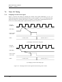
2.8.1.
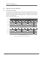
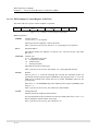
The ARM state register set
In ARM state, 16 general registers and one or two status registers are visible at any one time. In
privileged (non-User) modes, mode-specific banked registers are switched in.
Figure 2-2 : Register organization in ARM state shows which registers are available in each
mode: the banked registers are marked with a shaded triangle.
The ARM state register set contains 16 directly accessible registers: R0 to R15. All of these
except R15 are general-purpose, and may be used to hold either data or address values.
In addition to these, there is a seventeenth register used to store status information.
Register 14
is used as the subroutine link register. This receives a copy of R15 when a
Branch and Link (BL) instruction is executed. At all other times it may be
treated as a general-purpose register. The corresponding banked registers
R14_svc, R14_irq, R14_fiq, and R14_und are similarly used to hold the
return values of R15 when interrupts and exceptions arise, or when Branch
and Link instructions are executed within interrupt or exception routines.
Register 15
holds the Program Counter (PC). In ARM state, bits [1:0] of R15 are zero
and bits [31:2] contain the PC. In Thumb state, bit [0] is zero and bits
[31:1] contain the PC.
Register 16
is the CPSR (Current Program Status Register). This contains condition
code flags and the current mode bits.
FIQ mode has seven banked registers mapped to R8-14 (R8_fiq-R14_fiq). In ARM state, many
FIQ handlers do not need to save any registers. User, IRQ, Supervisor and Undefined each have
two banked registers mapped to R13 and R14, allowing each of these modes to have a private
stack pointer and link registers.
2-4
ML671000 User’s Manual
Chapter 2 CPU
ARM State General Registers and Program Counter
System & User
R0
R1
R2
R3
R4
R5
R6
R7
R8
R9
R10
R11
R12
R13
R14
R15(PC)
FIQ
Supervisor
R0
R1
R2
R3
R4
R5
R6
R7
R8_fiq
R9_fiq
R10_fiq
R11_fiq
R12_fiq
R13_fiq
R14_fiq
R15(PC)
R0
R1
R2
R3
R4
R5
R6
R7
R8
R9
R10
R11
R12
R13_svc
R14_svc
R15(PC)
IRQ
Undefined
R0
R1
R2
R3
R4
R5
R6
R7
R8
R9
R10
R11
R12
R13_irq
R14_irq
R15(PC)
R0
R1
R2
R3
R4
R5
R6
R7
R8
R9
R10
R11
R12
R13_und
R14_und
R15(PC)
CPSR
SPSR_irq
CPSR
SPSR_und
ARM State Program Status Registers
CPSR
CPSR
SPSR_fiq
CPSR
SPSR_svc
=banked register
Figure 2-2
Register organization in ARM state
2-5
ML67100 User’s Manual
Chapter 2 CPU
2.8.2.
The Thumb state register set
The Thumb state register set is a subset of the ARM state set. The programmer has direct access
to eight general registers, R0-R7, as well as the Program Counter (PC), a stack pointer register
(SP), a link register (LR), and the CPSR. There are banked Stack Pointers, Link Registers and
Saved Program Status Registers (SPSRs) for each privileged mode. This is shown in Figure 2-3:
Register organization in Thumb state.
Thumb State General Registers and Program Counter
System & User
R0
R1
R2
R3
R4
R5
R6
R7
SP
LR
PC
FIQ
R0
R1
R2
R3
R4
R5
R6
R7
SP _fiq
LR_fiq
PC
Supervisor
IRQ
R0
R1
R2
R3
R4
R5
R6
R7
SP_svc
LR_svc
PC
Undefined
R0
R1
R2
R3
R4
R5
R6
R7
SP_irq
LR_irq
PC
R0
R1
R2
R3
R4
R5
R6
R7
SP_und
LR_und
PC
CPSR
SPSR_irq
CPSR
SPSR_und
Thumb State Program Status Registers
CPSR
CPSR
SPSR_fiq
CPSR
SPSR_svc
=banked register
Figure 2-3
2-6
Register organization in Thumb state
ML671000 User’s Manual
Chapter 2 CPU
2.8.3.
The relationship between ARM and Thumb state registers
The Thumb state registers relate to the ARM state registers in the following way:
•
Thumb state R0-R7 and ARM state R0-R7 are identical
•
Thumb state CPSR and SPSRs and ARM state CPSR and SPSRs are identical
•
Thumb state SP maps onto ARM state R13
•
Thumb state LR maps onto ARM state R14
•
The Thumb state Program Counter maps onto the ARM state Program Counter (R15)
This relationship is shown in Figure 2-4: Mapping of Thumb state registers onto ARM state
registers.
Stack Pointer (SP)
Link Register (LR)
Program Counter (PC)
CPSR
SPSR
Figure 2-4
2.8.4.
R0
R1
R2
R3
R4
R5
R6
R7
R8
R9
R10
R11
R12
Stack Pointer (R13)
Link Register (R14)
Program Counter (R15)
CPSR
SPSR
Lo Registers
R0
R1
R2
R3
R4
R5
R6
R7
ARM State
Hi Registers
Thumb State
Mapping of Thumb state registers onto ARM state registers
Accessing Hi registers in Thumb state
In Thumb state, registers R8-R15 (the Hi registers) are not part of the standard register set.
However, the assembly language programmer has limited access to them, and can use them for
fast temporary storage.
A value may be transferred from a register in the range R0-R7 (a Lo register) to a Hi register, and
from a Hi register to a Lo register, using special variants of the MOV instruction. Hi register
values can also be compared against or added to Lo register values with the CMP and ADD
instructions.
2-7
ML67100 User’s Manual
Chapter 2 CPU
2.9.
The Program Status Registers
The CPU contains a Current Program Status Register (CPSR), plus four Saved Program Status
Registers (SPSRs) for use by exception handlers. These registers
•
hold information about the most recently performed ALU operation
•
control the enabling and disabling of interrupts
•
set the processor operating mode
The arrangement of bits is shown in Figure 2-5: Program status register format.
condition code flags
31
30
29
28
N
Z
C
V
(reserved)
27
26
25
24
control bits
23
8
7
6
5
I
F
T
4
3
Overflow
Carry/Borrow/Extend
Zero
Negative/Less Than
Figure 2-5
2.9.1.
2
1
0
M4 M3 M2 M1 M0
Mode bits
State bit
FIQ disable
IRQ disable
Program status register format
The condition code flags
The N, Z, C and V bits are the condition code flags. These may be changed as a result of
arithmetic and logical operations, and may be tested to determine whether an instruction should be
executed.
In ARM state, all instructions may be executed conditionally.
In Thumb state, only the Branch instruction is capable of conditional execution.
2.9.2.
The control bits
The bottom 8 bits of a PSR (incorporating I, F, T and M [4:0]) are known collectively as the
control bits. These will change when an exception arises. If the CPU is executing in a privileged
mode, they can also be manipulated by software.
The T bit
This reflects the operating state. When this bit is set, the CPU is executing in Thumb state,
otherwise it is executing in ARM state. Note that the software must never change the state of
the TBIT in the CPSR. If this happens, the CPU will enter an unpredictable state.
Interrupt disable bits
The I and F bits are interrupt disable bits.
When set, these disable the IRQ and FIQ interrupts respectively.
2-8
ML671000 User’s Manual
Chapter 2 CPU
The mode bits
The M4, M3, M2, M1 and M0 bits (M[4:0]) are the mode bits.
These determine the CPU's operating mode, as shown in Table 2-1 PSR mode bit values. Not
all combinations of the mode bits define a valid CPU mode. Only those explicitly described
shall be used.
The user should be aware that if any illegal value is programmed into the mode
then the CPU will enter an unrecoverable state.
bits,M[4:0],
If this occurs, reset should be applied.
Reserved bits
The remaining bits in the PSRs are reserved. When changing a PSR's flag or control bits, you
must ensure that these unused bits are not altered. Also, your program should not rely on them
containing specific values, since in future CPUs they may read as one or zero.
Table 2-1
PSR mode bit values
M[4:0]
Mode
Visible Thumb state registers
Visible ARM state registers
10000
User
R7..R0,
LR, SP
PC, CPSR
R14..R0,
PC, CPSR
10001
FIQ
R7..R0,
LR_fiq, SP_fiq
PC, CPSR, SPSR_fiq
R7..R0,
R14_fiq..R8_fiq,
PC, CPSR, SPSR_fiq
10010
IRQ
R7..R0,
LR_irq, SP_irq
PC, CPSR, SPSR_irq
R12..R0,
R14_irq..R13_irq,
PC, CPSR, SPSR_irq
10011
Supervisor
R7..R0,
LR_svc, SP_svc,
PC, CPSR, SPSR_svc
R12..R0,
R14_svc..R13_svc,
PC, CPSR, SPSR_svc
11011
Undefined
R7..R0
LR_und, SP_und,
PC, CPSR, SPSR_und
R12..R0,
R14_und..R13_und,
PC, CPSR
11111
System
R7..R0,
LR, SP
PC, CPSR
R14..R0,
PC, CPSR
2-9
ML67100 User’s Manual
Chapter 2 CPU
2.10.
Exceptions
Exceptions arise whenever the normal flow of a program has to be halted temporarily, for
example to service an interrupt from a peripheral. Before an exception can be handled, the current
CPU state must be preserved so that the original program can resume when the handler routine
has finished.
It is possible for several exceptions to arise at the same time. If this happens, they are dealt with in
a fixed order -see 2.10.9 Exception priorities.
2.10.1. Action on entering an exception
When handling an exception, the CPU:
1.
Preserves the address of the next instruction in the appropriate Link Register. If the
exception has been entered from ARM state, then the address of the next instruction is
copied into the Link Register (that is, current PC + 4 or PC + 8 depending on the exception.
See Table 2-2 Exception entry/exit for details). If the exception has been entered from
Thumb state, then the value written into the Link Register is the current PC offset by a
value such that the program resumes from the correct place on return from the exception.
This means that the exception handler need not determine which state the exception was
entered from.
For example, in the case of SWI, MOVS PC, R14_svc will always return to the next
instruction regardless of whether the SWI was executed in
ARM or Thumb state.
1.
Copies the CPSR into the appropriate SPSR
2.
Forces the CPSR mode bits to a value which depends on the exception
3. Forces the PC to fetch the next instruction from the relevant exception vector
It may also set the interrupt disable flags to prevent otherwise unmanageable nestings of
exceptions.
If the CPU is in Thumb state when an exception occurs, it will automatically switch into ARM
state when the PC is loaded with the exception vector address.
2-10
ML671000 User’s Manual
Chapter 2 CPU
2.10.2. Action on leaving an exception
On completion, the exception handler:
1.
Moves the Link Resister, minus an offset where appropriate, to the PC.(The offset will
vary depending on the type of exception.)
2.
Copies the SPSR back to the CPSR
3. Clears the interrupt disable flags, if they were set on entry
Note:
An explicit switch back to Thumb state is never needed, since restoring the CPSR from
the SPSR automatically sets the T bit to the value it held immediately prior to the exception.
2.10.3. Exception entry/exit summary
Table 2-2 : Exception entry/exit summarizes the PC value preserved in the relevant R14 on
exception entry, and the recommended instruction for exiting the exception handler.
Table 2-2 : Exception entry/exit
Return Instruction
Previous
ARM
R14_x
State
Thumb
R14_x
Notes
BL
MOV PC, R14
PC + 4
PC + 2
1
SWI
MOVS PC, R14_svc
PC + 4
PC + 2
1
UDEF
MOVS PC, R14_und
PC + 4
PC + 2
1
FIQ
SUBS PC, R14_fiq, #4 PC + 4
PC + 4
2
IRQ
SUBS PC, R14_irq, #4 PC + 4
PC + 4
2
RESET
NA
-
3
-
Note:
1.
Where PC is the address of the BL/SWI/Undefined Instruction.
2.
Where PC is the address of the instruction which did not get executed since the FIQ or
IRQ took priority.
3.
The value saved in R14_svc upon reset is unpredictable.
2-11
ML67100 User’s Manual
Chapter 2 CPU
2.10.4. FIQ
The FIQ (Fast Interrupt Request) exception is designed to support a data transfer or channel
process, and in ARM state has sufficient private registers to remove the need for register saving
(thus minimizing the overhead of context switching).
Irrespective of whether the exception was entered from ARM or Thumb state, a FIQ handler
should leave the interrupt by executing
SUBS PC, R14_fig, #4
FIQ may be disabled by setting the CPSR's F flag (but note that this is not possible from User
mode).
2.10.5. IRQ
The IRQ (Interrupt Request) exception is a normal interrupt. IRQ has a lower priority than FIQ
and is masked out when a FIQ sequence is entered. It may be disabled at any time by setting the I
bit in the CPSR, though this can only be done from a privileged (non-User) mode.
Irrespective of whether the exception was entered from ARM or Thumb state, an IRQ handler
should return from the interrupt by executing.
SUBS PC, R14_irq, #4
2.10.6. Software interrupt
The software interrupt instruction (SWI) is used for entering Supervisor mode, usually to request
a particular supervisor function. A SWI handler should return by executing the following
irrespective of the state (ARM or Thumb):
MOV PC, R14_svc
This restores the PC and CPSR, and returns to the instruction following the SWI.
2.10.7. Undefined instruction
When the CPU comes across an instruction which it cannot handle, it takes the undefined
instruction trap. This mechanism may be used to extend either the Thumb or ARM instruction set
by software emulation.
After emulating the failed instruction, the trap handler should execute the following irrespective
of the state (ARM or Thumb):
MOVS PC, R14_und
This restores the CPSR and returns to the instruction following the undefined instruction.
2-12
ML671000 User’s Manual
Chapter 2 CPU
2.10.8. Exception vectors
The following table shows the exception vector addresses.
Table 2-3
Exception vectors
Address
0x00000000
Exception
Reset
Mode on entry
Supervisor
0x00000004
Undefined instruction
Undefined
0x00000008
Software interrupt
Supervisor
0x0000000C
Reserved
Reserved
0x00000010
Reserved
Reserved
0x00000014
Reserved
Reserved
0x00000018
IRQ
IRQ
0x0000001C
FIQ
FIQ
2.10.9. Exception priorities
When multiple exceptions arise at the same time, a fixed priority system determines the order in
which they are handled:
Highest priority:
1
Reset
2
FIQ
3
IRQ
Lowest priority:
4
Undefined Instruction, software interrupt.
Not all exceptions can occur at once:
Undefined Instruction and Software Interrupt are mutually exclusive, since they each correspond
to particular (non-overlapping) decodings of the current instruction.
2-13
ML67100 User’s Manual
Chapter 2 CPU
2.11.
Reset
After a system reset, the CPU:
1.
Overwrites R14_svc and SPSR_svc by copying the current values of the PC and
into them. The value of the saved PC and SPSR is not defined.
2-14
2.
Forces M [4:0] to 10011(Supervisor mode), sets the I and F bits in the CPSR.
3.
Forces the PC to fetch the next instruction from address 0x00.
4.
Execution resumes in ARM state.
CPSR
Chapter 3
CPU Control Functions
3-1
ML671000 User’s Manual
Chapter 3 CPU Control Functions
3.1.
Overview
This LSI has the following CPU control functions.
3-2
• Reset processing:
A system reset initializes the CPU and on-chip peripherals.
• Clock control:
The oscillation circuit based on a crystal oscillator and a built-in
phase-locked loop together generate the system clock
(SYSCLK) signal. Changing the divider ratio adjusts the
operating clock frequency to match the processing load.
• Standby operation:
This portion controls transitions to the power saving HALT and
STOP modes as well as returns to normal operation.
ML671000 User’s Manual
Chapter 3 CPU Control Functions
3.1.1.
Pins
Table 3-1 lists the pins for the CPU control block.
Table 3-1 CPU Control Block Pins
Name
Symbol
Direction
Reset input
nRST
Input
Crystal oscillator
connection pin
OSC0
Input
Crystal oscillator
connection pin
OSC1
Output
CLKOUT
Output
PLLEN
Input
System clock output
PLL enable input
3.1.2.
Description
“L” level input from this pin produces a system
reset. “H” level input then starts instruction
execution from address 0.
Connect this pin to the crystal oscillator, ceramic
resonator, or the external clock supply.
Connect this pin to the crystal oscillator or
ceramic resonator. Leave this pin open if an
external clock supply is used.
This pin supplies the internal system clock
(SYSCLK) to outside devices.
Input “H” level activate the built-in phase-locked
loop. If an external clock signal with guaranteed
duty is available, “L” level this pin instead.
Control Registers
Table 3-2 lists the control registers for the CPU control block.
A read from these control registers takes 1 clock; a write, always at least two.
Writing to the standby control register (SBYCON) or clock control register (CKCON) is a 2step process: first write 0x0000003C to the register and then the desired value. Otherwise, there
is no change in the register contents.
Table 3-2 CPU Control Block Control Registers
Address
0x040_0000
0x040_0004
0x040_0008
0x040_000C
Name
Standby control register
Clock control register
Clock supply wait control register
Reset status register
Symbol
SBYCON
CKCON
CKWTCON
RSTST
Access
W
R/W
R/W
R
Size
32
32
32
32
Initial Value
0x00000000
0x00000000
0x00000000
0x00000000
3-3
ML671000 User’s Manual
Chapter 3 CPU Control Functions
3.2.
Detailed Control Register Descriptions
3.2.1.
Standby Control Register (SBYCON)
This write-only 32-bit register controls the HALT and STOP modes.
After a system reset, the contents are 0x00000000.
Do not simultaneously write “1” to both HLT and STP bits. Operation is not guaranteed.
31
30
-
-
---
3
-
2
-
1
STP
0
HLT
Dashes indicate nonexistent bits.
Figure 3-1 Standby Control Register (SBYCON)
■ Bit Descriptions
STP:
Stop mode bit. Writing “1” to this bit suspends all operation and shifts to the
STOP mode. This bit automatically returns to “0” when the LSI wakes from the
STOP mode.
HLT:
HALT mode bit. Writing “1” to this bit suspends CPU operation and shifts to the
HALT mode. On-chip peripherals, however, continue to operate. This bit
automatically returns to “0” when the LSI wakes from the HALT mode.
The LSI ignores writes to the STP and HLT bits, however, if there are interrupts pending—that
is,
(1) if a bit in an interrupt request register (IRR0 and IRR1) is “1,” and the corresponding
interrupt level control register (ILCONn, n=0 to 5) specifies a nonzero interrupt level (1 to
7) for that interrupt
(2) if the EFIQR bit in the external FIQ control register (EFIQCON) bit is “1,” and the EFIQM
bit in EFIQCON is “0,” enabling fast interrupt requests
For (1), either reset the interrupt request flag in the interrupt request registers (IRR0 and IRR1)
to “0” or set the interrupt level in the corresponding interrupt level control register (ILCONn,
n=0 to 5) to 0 before writing to SBYCON.
For (2), either reset the EFIQR bit to “0” or, before writing to this register, set the EFIQM bit to
"1" to mask fast interrupt requests.
3-4
ML671000 User’s Manual
Chapter 3 CPU Control Functions
3.2.2.
Clock Control Register (CKCON)
This 32-bit read/write register specifies the system clock (SYSCLK) supplied to the CPU and
on-chip peripherals.
After a system reset, the contents are 0x00000000.
31
-
30
-
---
3
-
2
-
1
0
CKM
Dashes indicate nonexistent bits. Reading one returns “0” in that position.
Figure 3-2 Clock Control Register (CKCON)
■ Bit Descriptions
CKM:
Clock multiplier
CKM
00
01
10
11
PLL in use
f x 1/2
f
Note:
Base frequency, f, is the internal clock frequency from the crystal oscillator
fx2
PLL not in use
f x 1/8
f x 1/4
f x 1/2
f
circuit or the external clock frequency from the OSC0 pin.
This field specifies the multiple for converting the input frequency, f, from the internal clock
source (base crystal oscillator circuit) or the external one (OSC0 pin input) to the system clock
(SYSCLK) for the CPU and on-chip peripherals: 2, 1, 1/2, 1/4, or 1/8. The selections available
depend on the source.
3-5
ML671000 User’s Manual
Chapter 3 CPU Control Functions
3.2.3.
Clock Supply Wait Control Register (CKWTCON)
This 32-bit read/write register specifies, for the crystal oscillator circuit and phase-locked loop,
a stabilization delay between the time that the LSI wakes from the STOP mode and the time
that it resumes supplying the clock signal.
After a system reset, the contents are 0x00000000.
Do not write a value outside the range 0x00000000 to 0x00000003 to CKWTCON.
31
30
---
3
2
-
-
-
-
-
1
0
CKWT
Dashes indicate nonexistent bits. Reading one returns “0” in that position.
Figure 3-3 Clock Supply Wait Control Register (CKWTCON)
■ Bit Descriptions
CKWT :
CKWT
00
01
10
11
Clock Count
32768
16384
1024
1
Delay (@12 MHz)
2.73 ms
1.36 ms
85.3 us
83.3 ns
This field specifies how long the LSI waits after waking from the STOP mode before restarting
the clock supply. After the corresponding number of clock cycles, the LSI supplies the
specified clock, whether the internal one by the crystal oscillator circuit or the external one
from the OSC0 pin, to the CPU and on-chip peripherals.
The 11b setting is for use only when both the source clock is an external one from the OSC0
pin and the phase-locked loop is not in use. If the phase locked loop is in use, the maximum
setting is 10b. If the clock is internal, choose 01b or 00b to allow sufficient time for the crystal
oscillator circuit—and the phase-locked loop, if in use—to stabilize.
3-6
ML671000 User’s Manual
Chapter 3 CPU Control Functions
3.2.4.
Reset Status Register (RSTST)
This read-only 32-bit register indicates the source of the last system reset. It contains
0x00000000 for external reset pin (nRST) input and 0x00000001 for watchdog timer overflow.
31
-
30
-
---
3
-
2
-
1
-
0
WDTRST
Dashes indicate nonexistent bits. Reading one returns “0” in that position.
Figure 3-4 Reset Status Register (RSTST)
■ Bit Descriptions
WDTRST: System reset source bit
External reset pin (nRST) input sets this bit to “0”; watchdog timer overflow, to
“1.”
3-7
ML671000 User’s Manual
Chapter 3 CPU Control Functions
3.3.
System Resets
This LSI has the following two system reset sources.
3.3.1.
•
External reset pin (nRST) input
•
Watchdog timer (WDT) overflow
Resetting with External Input
“L” level from the external reset pin (nRST) input asserts an internal reset signal for that
interval plus nine clock cycles, resetting the CPU and on-chip peripherals.
This type of reset has the following effects on the standby control (SBYCON) and reset status
(RSTST) registers.
3.3.2.
•
SBYCON goes to 0x00000000, waking the LSI from the standby modes (STOP or
HALT).
•
RSTST goes to 0x00000000. This type of reset does not insert a stabilization delay for the
crystal oscillator circuit and the phase-locked loop. The external system must, therefore,
assert the reset signal longer than the sum of the crystal oscillator circuit stabilization time
and PLL lock time.
Resetting with Watchdog Timer Overflow
Watchdog timer (WDT) overflow asserts the internal reset signal nine clock cycles, resetting
the CPU and all on-chip peripherals except the I/O ports and the CPU control block.
This type of reset does not reset the I/O ports or the CPU control block, so the settings for I/O
port directions (input or output), I/O port primary/secondary function selections, I/O port output
values, clock control (CKCON register), and clock supply delay (CKWTCON register) remain
the same as they were before the reset.
This type of reset has the following effects on the standby control (SBYCON) and reset status
(RSTST) registers.
SBYCON goes to 0x00000000, waking the LSI from the standby modes (STOP or HALT).
RSTST goes to 0x00000001.
3-8
ML671000 User’s Manual
Chapter 3 CPU Control Functions
3.4.
System Clock (SYSCLK)
A built-in phase-locked loop and frequency divider derive the system clock (SYSCLK)
supplied to the CPU and on-chip peripherals from the input frequency, f, from the internal
clock source (base crystal oscillator circuit) or the external one (OSC0 pin input).
If the base clock signal is the internal one, the STOP mode disables the crystal oscillator circuit.
Table 3-3 Clock Sources
Oscillation source
External clock
Crystal oscillator
OSC0
OSC1
Clock input
Open
Connect to crystal oscillator
Notes
Oscillation stops in STOP mode.
The CKM field in the clock control register (CKCON) specifies the multiple for converting the
base clock to the system clock (SYSCLK) for the CPU and on-chip peripherals. It is thus
possible for the user application to switch the operating clock frequency with processing load.
Table 3-4 System Clock Frequency Multipliers
CKM
00
01
10
11
Note:
System clock (SYSCLK)
PLL in use (PLLEN = “H”)
f x 1/2
f
fx2
PLL not in use (PLLEN = “L”)
f x 1/8
f x 1/4
f x 1/2
f
Base frequency, f, is the internal clock frequency from the crystal oscillator circuit or the
external clock frequency from the OSC0 pin.
3-9
ML671000 User’s Manual
Chapter 3 CPU Control Functions
3.5.
Standby Modes
3.5.1.
HALT Mode
Writing “1” to the HLT bit in the standby control register (SBYCON) shifts to the HALT mode,
suspending CPU operation, but leaving the on-chip peripherals operational.
The following wake the LSI from the HALT mode.
•
There is an external fast interrupt request (FIQ), and such interrupt requests are enabled
by the EFIQM bit in the external FIQ control register (EFIQCON).
•
There is an external interrupt request with a nonzero interrupt level. (See Note.)
•
There is an internal interrupt request with a nonzero interrupt level. (See Note.)
•
External reset pin (nRST) input or watchdog timer (WDT) overflow produces a system
reset.
■ Note ■
If the interrupt level for an external or internal interrupt request is between 1 and the current
interrupt level, the interrupt request terminates HALT mode, but does not reach the CPU itself.
3-10
ML671000 User’s Manual
Chapter 3 CPU Control Functions
3.5.2.
STOP Mode
Writing “1” to the STP bit in the standby control register (SBYCON) shifts to the STOP mode,
shutting down the CPU, the crystal oscillator circuit, the phase-locked loop, and thus the onchip peripherals. (Note 1)
The following wake the LSI from the STOP
mode.
•
There is an external fast interrupt request (FIQ), and such interrupt requests are enabled
by the EFIQM bit in the external FIQ control register (EFIQCON).
•
There is an external interrupt request with a nonzero interrupt level. (See Note.)
•
There is a USB suspend mode start/end interrupt request with a nonzero interrupt level.
(See Note.)
•
External reset pin (nRST) input produces a system reset.
■ Note 1■
If the interrupt level for an external or internal interrupt request is between 1 and the current
interrupt level, the interrupt request terminates HALT mode, but do11s not reach the CPU
itself.
When the LSI wakes from the STOP mode, it restarts the crystal oscillator circuit, inserts a wait
to allow sufficient time for the crystal oscillator circuit—and the phase-locked loop, if in use—
to stabilize, and, when that time has elapsed, resumes supplying the system clock to the CPU
and on-chipperipherals. Note that an external reset does not insert a wait.
■ Note 2■
The crystal oscillator circuit, phase-locked loop, and USB device controller remain operational
in the STOP mode if USB device controller OSC control is enabled, and the USB device
controller is not in the suspend state.
3-11
ML671000 User’s Manual
Chapter 3 CPU Control Functions
3.6.
Clock Supply Delay
The CKWT field in the clock supply wait control register (CKWTCON) specifies how long the
LSI waits after waking from the STOP mode before restarting the clock supply to the CPU and
on-chip peripherals. Note that this setting applies even when the built-in phase-locked loop is
not in use.
An external reset during STOP mode does not insert this wait. The external system must,
therefore, assert the reset signal long enough to allow sufficient time for the crystal oscillator
circuit—and the phase-locked loop, if in use—to stabilize.
Table 3-5 Clock Supply Delay
CKWT
00
01
10
11
Clock Count
32768
16384
1024
1
Delay (@12 MHz)
2.73 ms
1.36 ms
85.3us
83.3 ns
The 11b setting is for use only when both the source clock is an external one from the OSC0
pin and the phase-locked loop is not in use. If the phase-locked loop is in use, the maximum
setting is 10b. If the clock is internal, choose 01b or 00b to allow sufficient time for the crystal
oscillator circuit—and the phase-locked loop, if in use—to stabilize.
3-12
Chapter 4
Interrupt Controller
4-1
ML671000 User’s Manual
Chapter 4 Interrupt Controller
4.1.
Overview
The interrupt controller supports up to a maximum of 22 interrupt sources: one external fast interrupt
request (FIQ), eight external interrupts, and thirteen internal interrupts. Interrupt sources are
assigned one of eight priority levels for use in providing program control over processing
precedence.
•
The interrupt controller supports external FIQ interrupts from the nEFIQ pin, eight
external interrupts from the nEIR[7:0] pins, and up to thirteen internal interrupts from the
serial communications interface and other on-chip peripherals.
•
There are eight interrupt priority levels available for use in providing program control over
processing precedence.
•
The interrupt controller maps each interrupt source to a predetermined interrupt, which the
LSI uses to quickly branch to the corresponding interrupt service routine.
4-2
ML671000 User’s Manual
Chapter 4 Interrupt Controller
4.1.1.
Block Diagram
Figure 4-1 shows a block diagram for the interrupt controller.
The interrupt controller consists of the following registers, circuits, and other components.
•
Interrupt number register (INR) holding the interrupt number for the interrupt request with the
highest priority
•
Current interrupt level register (CILR) holding the interrupt level of the interrupt currently
being processed
•
Interrupt request level register (IRLR) holding the highest interrupt level of the interrupts
currently pending
•
External FIQ control register (EFIQCON) containing control and status bits for external fast
interrupt requests (FIQs)
•
External interrupt control register (EIRCON) specifying external interrupt sensing methods
•
Interrupt request registers (IRR0 and IRR1) containing interrupt request flags for each interrupt
•
Interrupt level control registers (ILCONn, n=0 to 5) specifying the interrupt level settings for
each interrupt
•
Interrupt acceptance circuitry
•
Priority level judgment circuitry
External FIQ
acceptance
circuitry
External FIQs from
nEFIQ pin
External FIQ
control register
(EFIQCON)
nFIQ
W KUPRQ
Peripheral bus
Ext ernal
int errupt
control regist er
(EIRCON)
External interrupt
requests from
EIR[7:0] pins
Internal interrupt
requests
Int errupt level
control regist er
(ILCONn, n=0 t o 5)
Current
int errupt
level
regist er
(CILR)
Int errupt
request level
regist er
(IRLR)
Int errupt
number
regist er
(INR)
8
13
External and internal
interrupt
acceptance
circuitry
Priority level judgement circuitry
Interrupt request
registers
(IRR0,IRR1)
nIRQ
nFIQ and nIRQ are exception request signals to the CPU.
WKUPRQ is a wake-up request for releasing the LSI from standby modes (STOP or HALT).
Figure 4-1
Interrupt Controller Block Diagram
4-3
ML671000 User’s Manual
Chapter 4 Interrupt Controller
4.1.2.
Pins
Table 4-1 lists the pins for the interrupt controller.
Table 4-1
Name
External FIQ
External interrupt
request
4.1.3.
Interrupt Controller Pins
Symbol
Direction
nEFIQ
Input
nEIR[7:0]
Input
Description
Fast interrupt request (FIQ) input pin
external interrupt input pins. These
represent the secondary functions for the
pins P2[7:0].
Control Registers
Table 4-2 lists the control registers for the interrupt controller.
Table 4-2
Address
Interrupt Controller Control Registers
Name
Symbol
R/W
Size
Initial
Value
0x060_0000
Interrupt number register
INR
R
8
Indeterminate
0x060_0004
Current interrupt level register
CILR
R/W
8
0x00
0x060_0008
Interrupt request level register
IRLR
R
8
0x00
0x060_000C
External FIQ control registers
EFIQCON
R/W
8
0x04/06
0x060_0010
External interrupt control registers
EIRCON
R/W
8
0x00
0x060_0014
Interrupt request register 0
IRR0
R/W
8/16
0x060_0018
Interrupt request register 1
IRR1
R/W
8
0x060_0020
Interrupt level control register 0
ILCON0
R/W
8/16
0x0000
0x060_0024
Interrupt level control register 1
ILCON1
R/W
8/16
0x0000
0x060_0028
Interrupt level control register 2
ILCON2
R/W
8/16
0x0000
0x060_002C
Interrupt level control register 3
ILCON3
R/W
8/16
0x0000
0x060_0030
Interrupt level control register 4
ILCON4
R/W
8/16
0x0000
0x060_0034
Interrupt level control register 5
ILCON5
R/W
8/16
0x0000
4-4
0x0000
0x00
ML671000 User’s Manual
Chapter 4 Interrupt Controller
4.2.
Interrupt Sources
There are two basic interrupt sources: external FIQ interrupt requests generating FIQ exceptions and
external and internal interrupt requests generating IRQ exceptions. External FIQ interrupt requests,
if enabled, always produce FIQ exception requests to the CPU.
External and internal interrupt requests, if enabled, produce IRQ exception requests to the CPU only
if the interrupt level specified for the source is higher than the current interrupt level, the level for
the interrupt currently being processed. If the former is the same as or lower than the latter, the
interrupt request is held pending until the current interrupt level drops below the corresponding
interrupt level.
4.2.1.
External FIQ Interrupt Requests
If the EFIQM bit in the external FIQ control register (EFIQCON) is “0” indicating no masking, a
falling edge in the input signal from the external FIQ interrupt request pin (nEFIQ) produces an FIQ
exception request to the CPU. The CPU only accepts the request, however, if the F bit in its current
program status register (CPSR) is “0.”
In the STOP mode, the trigger is always “L” level input.
4.2.2.
External Interrupt Requests
If the interrupt level specified for the source is higher than the current interrupt level, a falling edge
or “L” level input—the corresponding bits in the external interrupt control register (EIRCON)
specifies which—in an nEIR[7:0] input signal produces an IRQ exception request to the CPU. The
CPU only accepts the request, however, if the I bit in its current program status register (CPSR) is
“0.”
In the STOP mode, the trigger is always “L” level input regardless of the EIRCON setting.
4.2.3.
Internal Interrupt Requests
The following on-chip peripherals generate internal interrupt requests.
•
USB device controller (USBC)
•
UART
•
Serial communications interface (SCI)
•
Time base generator (TBG)
•
Timers (TMn, n=0 to 3)
•
DMA controller (DMAC)
If the interrupt level specified for the interrupt request is higher than the current interrupt level—that
is higher in priority—the interrupt controller sends an IRQ exception request to the CPU. The CPU
only accepts the request, however, if the I bit in its current program status register (CPSR) is “0.”
4-5
ML671000 User’s Manual
Chapter 4 Interrupt Controller
4.2.4.
Interrupt Sources, Interrupt Numbers, and Control Registers
Table 4-3 lists the interrupt sources, their interrupt numbers, the corresponding request flags in the
interrupt request registers (IRR0 and IRR1), the interrupt level control register (ILCONn, n=0 to 5)
fields specifying their interrupt levels, and, in the last column, the precedence for simultaneously
arriving multiple interrupts with the same interrupt levels.
The symbols in the first column the following meanings.
EFIQ
:
Fast interrupt request (FIQ) from nEFIQ pin
EIR[n] (n=0 to 7)
:
External interrupt request from nEIR[n] pin
TMEVENT0
:
Capture event/compare match interrupt from Timer 0
TMEVENT1
:
Capture event/compare match interrupt from Timer 1
TMOV0
:
Timer overflow interrupt from Timer 0
TMOV1
:
Timer overflow interrupt from Timer 1
TMOV2
:
Timer overflow interrupt from Timer 2
TMOV3
:
Timer overflow interrupt from Timer 3
WDINT
:
Overflow interrupt from time base generator
USBEVENT
:
Event interrupt from USB device controller
DMAEVENT
:
Event interrupt from DMA controller
SCIEVENT
:
Event interrupt from serial communications interface
BGINT
:
Baud rate generator interrupt from serial communications interface
UARTEVENT
:
Event interrupt from UART port
USBSINT
:
Suspended state interrupt from USB device controller
4-6
ML671000 User’s Manual
Chapter 4 Interrupt Controller
Table 4-3
Source
Interrupt Sources, Interrupt Numbers, Interrupt Request Flags,
and Level Control Registers
Interrupt
Interrupt
Number
Request Flag
Interrupt Level Field in
Interrupt Level Control
Registers
EFIQ
–
EFIQR
–
EIR[7]
23
IRR1[7]
ILR23
EIR[6]
22
IRR1[6]
ILR22
EIR[5]
21
IRR1[5]
ILR21
EIR[4]
20
IRR1[4]
ILR20
EIR[3]
19
IRR1[3]
ILR19
EIR[2]
18
IRR1[2]
ILR18
EIR[1]
17
IRR1[1]
ILR17
EIR[0]
16
IRR1[0]
ILR16
Reserved
15
IRR0[15]
ILR15
Reserved
14
IRR0[14]
ILR14
Reserved
13
IRR0[13]
ILR13
USBEVENT
12
IRR0[12]
ILR12
TMEVENT1
11
IRR0[11]
ILR11
TMOV1
10
IRR0[10]
ILR10
TMEVENT0
9
IRR0[9]
ILR9
TMOV0
8
IRR0[8]
ILR8
TMOV3
7
IRR0[7]
ILR7
TMOV2
6
IRR0[6]
ILR6
WDINT
5
IRR0[5]
ILR5
DMAEVENT
4
IRR0[4]
ILR4
SCIEVENT
3
IRR0[3]
ILR3
BGINT
2
IRR0[2]
ILR2
UARTEVENT
1
IRR0[1]
ILR1
USBSINT
0
IRR0[0]
ILR0
Predetermined
Priority Level
–
High
Low
4-7
ML671000 User’s Manual
Chapter 4 Interrupt Controller
4.3.
Detailed Control Register Descriptions
4.3.1.
Interrupt Number Register (INR)
This read-only 8-bit register holds the interrupt number for the current interrupt with the highest
precedence.
After a system reset, the contents are indeterminate.
7
-
6
-
5
-
4
3
2
1
0
Dashes indicate nonexistent bits. Reading one returns “0” in that position.
Figure 4-2
Interrupt Number Register (INR)
INR bits 4 to 0 give the interrupt number for the current interrupt with the highest precedence. This
number, between 0 and 23, gives the source.
Read the contents of this register only once per IRQ exception because they are invalid between the
first read and the next interrupt request.
4.3.2.
Current Interrupt Level Register (CILR)
This 8-bit read/write register holds the current interrupt level, the interrupt level specified for the
interrupt currently being processed.
After a system reset, the contents are 0x00.
7
6
5
4
3
2
1
0
-
Dashes indicate nonexistent bits. Reading one returns “0” in that position.
Figure 4-3
Current Interrupt Level Register (CILR)
Reading the interrupt number register (INR) sets the CILR bit corresponding to interrupt level value
specified in the interrupt request level register (IRLR) to “1.”
Writing “1” to a bit resets that bit to “0”; “0” produces no change.
The interrupt controller uses the top seven CILR bits to mask lower level interrupts. The following is
a list of the correspondences.
CILR[7]
level 7 interrupts
CILR[6]
level 6 interrupts
:
CILR[1]
4-8
:
level 1 interrupts
ML671000 User’s Manual
Chapter 4 Interrupt Controller
4.3.3.
Interrupt Request Level Register (IRLR)
This read-only 8-bit register holds the interrupt level, specified in the corresponding interrupt level
field (ILRn, n=0 to 23) in the interrupt level control registers (ILCONn, n=0 to 5), for the currently
pending unmasked interrupt with the highest precedence.
After a system reset, the contents are 0x00.
7
-
6
-
5
-
4
-
3
-
2
1
0
Dashes indicate nonexistent bits. Reading one returns “0” in that position.
Figure 4-4
Interrupt Request Level Register (IRLR)
This register holds the interrupt level for the currently pending unmasked interrupt with the highest
precedence. The contents are the number, between 1 and 7, from the corresponding interrupt level
field (ILRn, n=0 to 23) in the interrupt level control registers (ILCONn, n=0 to 5).
The IRQ handler must read this register before the interrupt number register (INR) because reading
the latter resets the contents to 0x00.
4.3.4.
External FIQ Control Register (EFIQCON)
This 8-bit read/write register controls masking of external FIQ interrupt requests, monitors the
nEFIQ pin input level, and holds the FIQ interrupt request flag.
After a system reset, the contents are 0x04 or 0x06.
7
-
6
-
5
-
4
-
3
-
2
1
0
EFIQM
EFIQS
EFIQR
Dashes indicate nonexistent bits. Reading one returns “0” in that position.
Figure 4-5
External FIQ Control Register (EFIQCON)
■ Bit Descriptions
EFIQM:
External FIQ mask bit
Setting this bit to “1” masks external FIQ interrupts; “0” disables masking.
EFIQS:
nEFIQ pin level monitor
Reading this bit yields “0” for “L” level input from nEFIQ; “1” for “H” level.
Writes to this bit are ignored.
EFIQR:
External fast interrupt request (FIQ)
A falling edge in the input signal from the nEFIQ sets this bit to “1,” indicating an
external FIQ request. Writing “1” to this bit resets it to “0”; “0” produces no change.
4-9
ML671000 User’s Manual
Chapter 4 Interrupt Controller
4.3.5.
External Interrupt Control Register (EIRCON)
This 8-bit read/write register specifies external interrupt sensing methods: “L” level input (level
sensing) or falling edge (edge sensing).
After a system reset, the contents are 0x00.
In the STOP mode, the trigger is always “L” level input regardless of the EIRCON setting.
7
6
5
4
3
2
1
0
EIR7
EIR6
EIR5
EIR4
EIR3
EIR2
EIR1
EIR0
Figure 4-6
External Interrupt Control Register (EIRCON)
■ Bit Descriptions
EIRn:
4.3.6.
(n=0 to 7)
Sensing control for external interrupt pin nEIR[n]
A “1” specifies falling edge input; “0,” “L” level input.
The specified trigger in the input signal sets the corresponding bit in the interrupt
request registers (IRR0 and IRR1) to “1.”
Interrupt Request Registers (IRR0 and IRR1)
These read/write registers contain interrupt request flags for each interrupt. IRR0 is 16 bits wide;
IRR1, 8 bits.
Table 4-3 above gives the correspondences between the bits in these registers and the interrupt
sources.
After a system reset, the contents are both zero—0x0000 and 0x00, respectively.
IRR0
15
-
14
-
13
-
12
11
10
9
8
6
5
4
3
2
1
0
7
6
5
4
3
2
1
IRR1
7
Dashes indicate nonexistent bits. Reading one returns “0” in that position.
Figure 4-7
Interrupt Request Registers (IRR0 and IRR1)
An interrupt request from the corresponding interrupt source sets the bit to “1,” indicating an
interrupt request.
Writing “1” to a bit resets that bit to “0”; “0” produces no change.
4-10
0
ML671000 User’s Manual
Chapter 4 Interrupt Controller
4.3.7.
Interrupt Level Control Registers (ILCONn, n=0 to 5)
These 16-bit read/write registers specify the interrupt levels for each interrupt source.
After a system reset, the contents are all 0x0000.
There are eight interrupt priority levels available for use in providing program control over
processing precedence.
Figure 4-8 shows the locations of the interrupt level fields (ILRn, n=0 to 23) for each interrupt
source using the numbers from Table 4-3 above.
In an interrupt level field, the setting 7 produces the highest priority level. The smaller the value, the
lower the priority level. Level 0 masks the corresponding interrupt requests.
ILCON0
15
14
-
13
12
ILR3
11
10
-
9
8
ILR2
7
6
-
5
4
ILR1
3
2
-
1
0
ILR0
ILCON1
15
14
-
13
12
ILR7
11
10
-
9
8
ILR6
7
6
-
5
4
ILR5
3
2
-
1
0
ILR4
ILCON2
15
14
-
13
12
ILR11
11
10
-
9
8
ILR10
7
6
-
5
4
ILR9
3
2
-
1
0
ILR8
ILCON3
15
14
-
13
12
(ILR15)
11
10
-
9
8
(ILR14)
7
6
-
5
4
(ILR13)
3
2
-
1
0
ILR12
ILCON4
15
14
-
13
12
ILR19
11
10
-
9
8
ILR18
7
6
-
5
4
ILR17
3
2
-
1
0
ILR16
ILCON5
15
-
14
13
12
ILR23
11
-
10
9
ILR22
8
7
-
6
5
ILR21
4
3
-
2
1
ILR20
Dashes indicate nonexistent bits. Reading one returns “0” in that position.
Figure 4-8
Interrupt Level Control Registers (ILCONn, n=0 to 5)
4-11
0
ML671000 User’s Manual
Chapter 4 Interrupt Controller
4.4.
Interrupt Processing
4.4.1.
External FIQ Interrupts
An external FIQ interrupt request, if not masked by the EFIQM bit in the external FIQ control
register (EFIQCON), produces an FIQ exception request to the CPU.
4.4.1.1. Interrupt Sequence
1. Interrupt request:
An external FIQ interrupt request arrives.
2. Interrupt request flag:
The interrupt controller notes the request by setting the EFIQR bit in the external FIQ control
register (EFIQCON) to “1.”
3. Exception request to CPU:
If the EFIQM bit in EFIQCON is not “1,” the interrupt controller asserts the nFIQ signal to
produce an FIQ exception request to the CPU.
4. Exception acceptance:
If the CPU is ready to accept the exception—that is, the F bit in the current program status
register (CPSR) enables FIQ exceptions—it switches to the FIQ exception handler and sets the
F and I bits in CPSR to “1” to disable further FIQ and IRQ exceptions.
5. Handler:
In addition to the normal interrupt processing, the FIQ handler writes “1” to the EFIQR bit to
clear the interrupt request and negate the nFIQ signal.
6. Return from interrupt:
The CPU executes the return from interrupt instruction.
4-12
ML671000 User’s Manual
Chapter 4 Interrupt Controller
4.4.2.
External and Internal Interrupts
The interrupt controller determines the following as specified in Table 4-3.
•
Interrupt number
•
Request flag position in the interrupt request registers (IRR0 and IRR1)
•
Interrupt level field (ILRn, n=0 to 23) in the interrupt level control registers (ILCONn, n=0
to 5)
•
Predetermined priority level
4.4.2.1. Interrupt Priority Levels
The following procedure determines the interrupt request priority level.
1.
If the interrupt request interrupt level is higher than the current interrupt level, the interrupt
level specified for the interrupt currently being processed, the interrupt controller asserts the
nIRQ signal to produce an IRQ exception request to the CPU.
2.
If there are multiple interrupt requests, the one with the highest interrupt level takes precedence.
3.
If there are multiple interrupt requests with that interrupt level, the one with the highest
predetermined interrupt level takes precedence.
The interrupt controller copies the interrupt level specified for interrupt request thus selected to the
interrupt request level register (IRLR) and its interrupt number to the interrupt number register
(INR).
4-13
ML671000 User’s Manual
Chapter 4 Interrupt Controller
4.4.2.2. Interrupt Sequence
1. Interrupt request:
An external interrupt request or an internal one from the on-chip peripherals arrives.
2. Interrupt request flag:
The interrupt controller notes the request by setting the corresponding bit in the interrupt
request registers (IRR0 and IRR1) to “1.”
3. Exception request to CPU:
If the interrupt level is not 0, the mask state, the interrupt controller processes the interrupt
request with the following three steps.
•
If there any interrupt requests with interrupt levels higher than that in the current
interrupt level register (CILR), the interrupt controller asserts the nIRQ signal to produce
an IRQ exception request to the CPU.
•
The interrupt controller copies the highest such interrupt level found among the pending
interrupt requests to the interrupt request level register (IRLR).
•
The interrupt controller copies the interrupt number, determined using the procedure in
step (2) in Section 4.4.2.1 “Interrupt Priority Levels” above, to the interrupt number
register (INR).
4. Exception acceptance:
If the CPU is ready to accept the exception—that is, the I bit in the current program status
register (CPSR) enables IRQ exceptions—it switches to the IRQ exception handler and sets the
I bit in CPSR to “1” to disable further IRQ exceptions.
5. Source determination:
The IRQ handler reads the interrupt number from the interrupt controller's interrupt number
register (INR) and sets the CILR bit corresponding to that interrupt level to “1,” negating the
nIRQ signal.
6. Handler:
In addition to the normal interrupt processing, the IRQ
handler executes the following steps.
•
It prepares to accept interrupt requests with interrupt levels even higher than the one
currently being processed by saving the link register (R14_irq) and the saved program
status register (SPSR_irq) to the stack.
•
It resets the I bit in CPSR to “0” to enable further IRQ exceptions.
•
It writes “1” to the corresponding interrupt request flag in the interrupt request registers
(IRR0 and IRR1) to clear the interrupt request.
7. Return from interrupt:
The CPU resets the CILR bit for the current interrupt level to “0” and executes the return from
interrupt instruction.
4-14
ML671000 User’s Manual
Chapter 4 Interrupt Controller
4.4.2.3. Interrupt Level Control Example
Figure 4-9 gives an example of a level 2 interrupt service routine interrupted by a level 7 interrupt
request, which in turn is interrupted by an FIQ interrupt request.
t1. Level 2 interrupt request
The interrupt controller sets the interrupt request level register (IRLR) to 2. It simultaneously
asserts the nIRQ signal to produce an IRQ exception request to the CPU.
t2. IRQ exception acceptance
The CPU accepts the request and switches to the IRQ handler.
t3. INR readout
The IRQ handler reads the interrupt number register (INR). Because the interrupt request
level register (IRLR) contains 2, the interrupt controller sets bit 2 (CILR[2]) in the current
interrupt level register (CILR) to “1,” negating the nIRQ signal.
t4. Shift to level 2 interrupt service routine
To prepare to accept interrupt requests with higher interrupt levels, the level 2 interrupt service
routine saves the link register (R14_irq) and the saved program status register (SPSR_irq) to
the stack. It then resets the I bit in CPSR to “0.”
t5. Level 7 interrupt request
The interrupt controller sets the interrupt request level register (IRLR) to 7. It simultaneously
asserts the nIRQ signal to produce an IRQ exception request to the CPU.
t6. IRQ exception acceptance
The CPU accepts the request and switches to the IRQ handler.
t7. INR readout
The IRQ handler reads the interrupt number register (INR). Because the interrupt request level
register (IRLR) contains 7, the interrupt controller sets bit 7 (CILR[7]) in the current interrupt
level register (CILR) to “1,” negating the nIRQ signal.
t8. Shift to level 7 interrupt service routine
To prepare to accept interrupt requests with higher interrupt levels, the level 7 interrupt service
routine saves the link register (R14_irq) and the saved program status register (SPSR_irq) to
the stack. It then resets the I bit in CPSR to “0.”
t9. FIQ interrupt request
The interrupt controller asserts the nFIQ signal to produce an FIQ exception request to the
CPU.
t10. FIQ exception acceptance
The CPU accepts the request and switches to the FIQ handler.
t11. EFIQR clear
The FIQ handler resets the EFIQR bit to “0” to clear the interrupt request, negating the nFIQ
signal.
t12. Return from FIQ handler
The FIQ handler executes the SUBS PC, R14_fiq, #4 instruction to restore the link register
(R14_irq) and the saved program status register (SPSR_irq) to their contents before the FIQ
interrupt request.
4-15
ML671000 User’s Manual
Chapter 4 Interrupt Controller
t13. Level 7 interrupt request clear
The level 7 interrupt service routine writes “1” to the corresponding bit in the interrupt request
registers (IRR0 and IRR1) to clear the interrupt request currently being processed.
t14. CILR[7] clear
Before returning, the level 7 interrupt service routine resets CILR[7] to “0.”
t15. Return from interrupt service routine
The level 7 interrupt service routine executes the SUBS PC, R14_fiq, #4 instruction to restore
the link register (R14_irq) and the saved program status register (SPSR_irq) to their contents
before the level 7 interrupt request.
t16. Level 2 interrupt request clear
The level 2 interrupt service routine writes “1” to the corresponding bit in the interrupt request
registers (IRR0 and IRR1) to clear the interrupt request currently being processed.
t17. CILR[2] clear
The CPU sets the I bit in CPSR to “1” to disable further IRQ exceptions.
Before returning, the level 2 interrupt service routine resets CILR[2] to “0.”
t18. Return from interrupt service routine
The level 2 interrupt service routine executes the SUBS PC, R14_fiq, #4 instruction to restore
the link register (R14_irq) and the saved program status register (SPSR_irq) to their contents
before the level 2 interrupt request.
t1
t2
t3
t4
t5
t6
t7
t8
t9
t 10
t 11
t 12
t 13
t 14
t 15
t 16
t 17
t 18
Interrupt p roces s in g
FIQ h andler
Level 7 interrup t
proces s ing
Level 2 interrup t
proces s ing
IRQ h andler
Normal p roces s in g
Interrupt controller
nFIQ
nIRQ
CILR
IRLR
Interrupt requ es t
00 000 00
0
00 000 100
2
0
Level 2 in t errup t request
Level 7 in t errup t
request
Figure 4-9
4-16
10 000 100
7
00 000 100
00 000 00
Ex t ernal FIQ in t errup t
request
Interrupt Level Control Example
00 000 000
ML671000 User’s Manual
Chapter 4 Interrupt Controller
4.5.
Sampling Timing for External Interrupt Requests
The interrupt controller sets the interrupt request bits for the external FIQ interrupt requests and
external interrupt requests based on its sampling of the input signals from the nEFIQ and nEIR[7:0]
pins.
Figure 4-10 shows the timing for sampling the external FIQ interrupt request signal and setting the
EFIQR bit in the external FIQ control register (EFIQCON).
The interrupt controller samples the nEFIQ pin input at the rising edges of the system clock
(SYSCLK). If this sampling reveals a transition from “H” level to “L,” the interrupt controller sets
the EFIQR bit to “1” at the next SYSCLK rising edge to produce an FIQ exception request to the
CPU.
Because of this sampling timing, the width of the “H” and “L” level pulses in the nEFIQ pin input
must be at least two system clock (SYSCLK) periods.
SYSCLK
(CLKOUT)
nEFIQ pin
Set to "1"
EFIQR bit
Figure 4-10
Sampling Timing for FIQ Input
Figure 4-11 shows the timing for sampling the external interrupt request signal and setting the
corresponding interrupt request bit in interrupt request register 1(IRR1).
The interrupt controller samples the nEIR[7:0] pin input at the rising edges of the system clock
(SYSCLK). If the external interrupt control register (EIRCON) specifies a falling edge as the
interrupt trigger, and this sampling reveals a transition from “H” level to “L,” the interrupt controller
sets the corresponding interrupt request bit in interrupt request register 1 (IRR1) at the next
SYSCLK rising edge to produce an IRQ exception request to the CPU.
If the external interrupt control register (EIRCON) specifies “L” level input as the interrupt trigger,
and this sampling reveals same, the interrupt controller sets the corresponding interrupt request bit in
interrupt request register 1 (IRR1) at the next SYSCLK rising edge to produce an IRQ exception
request to the CPU.
It continues doing so as long as there is “L” level input at each sampling interval.
Because of this sampling timing, the width of the “H” and “L” level pulses in the nEIR[7:0] pin
input must be at least two system clock (SYSCLK) periods.
4-17
ML671000 User’s Manual
Chapter 4 Interrupt Controller
SYSCLK
(CLKOUT)
nEIR[7:0] pin
Set to "1"
Interrupt request
bit in IRR1
(a) falling edge as interrupt trigger
SYSCLK
(CLKOUT)
nEIR[7:0] pin
Set to "1"
Interrupt request
bit in IRR1
(b) “L” level input as interrupt trigger
Figure 4-11
4-18
Sampling External Interrupt Request Signals
ML671000 User’s Manual
Chapter 4 Interrupt Controller
4.6.
Interrupt Latency
Table 4-4 summarizes the interrupt latency (response time) between the interrupt request and the
fetching of the instruction at the exception vector address.
Note that CPU acceptance of FIQ and IRQ exceptions is delayed until the following obstacles have
been removed.
•
The interrupt is masked inside the interrupt controller.
•
The interrupt level for the interrupt being processed is the same as or lower than the
current interrupt level.
•
The F or I bit in the CPU's current program status register (CPSR) is “1.”
Table 4-4
Interrupt Latency
Clock cycles
Item
Delay between interrupt
trigger at interrupt signal pin
and setting of interrupt
request flag
External interrupt
request (FIQ
interrupt or external
interrupt)
Internal
interrupt request
2
–
Time required to complete
currently executing
instruction
X (at least 1)
The minimum is one clock
cycle. The maximum, 20 clock
cycles, is for an LDM
instruction loading all 16
general-purpose registers.
2M
M is the instruction fetch
cycle. Before fetching the
instruction at the vector
address, the CPU executes two
dummy instruction fetches.
Time to save PC and CPSR
to the stack and fetch
instruction at vector address
Interrupt
latency
Notes
Total
X+2M+2
X+2M
Minimum delay
5
3
4-19
ML671000 User’s Manual
Chapter 4 Interrupt Controller
4.7.
Notes on Processing Interrupts
1.
Reading interrupt number register (INR)
Read the contents of this register only once per IRQ exception because they are invalid
between the first read and the next interrupt request.
2.
Reading interrupt request level register (IRLR)
The IRQ handler must read this register before the interrupt number register (INR) because
reading the latter resets the contents to 0x00.
3.
Processing invalid interrupt requests
In the interval between when the CPU accepts an IRQ exception request and when it transfers
control to the IRQ handler, the following actions trigger spurious interrupt requests that
invalidate the contents of both the interrupt number (INR) and interrupt request level (IRLR)
registers.
•
Setting the interrupt request's interrupt level lower than the current interrupt level.
•
Masking the interrupt request by setting its interrupt level to zero.
•
Clearing the interrupt request by setting its interrupt request flag in the interrupt request
registers (IRR0 and IRR1) to "0."
These spurious interrupt requests reset both the interrupt number (INR) and interrupt request
level (IRLR) registers to 0x00. They do not affect the contents of the current interrupt level
register (CILR).
If the user application program changes interrupt levels or clears interrupt requests outside the
IRQ handler and initialization routine, therefore, the IRQ handler must incorporate the
following logic to detect these spurious interrupt requests.
(1) Read the contents of the interrupt request level register (IRLR).
(2) If the contents are 0x00, return from the IRQ handler.
If the IRLR contents are not 0x00, it is safe for the IRQ handler to read the contents of the
interrupt number register (INR) and continue.
If changing the interrupt level produces a spurious interrupt request, there is an IRQ exception
request when that interrupt's interrupt level becomes higher than the current interrupt level.
4-20
Chapter 5
I/O Ports
5-1
ML671000 User’s Manual
Chapter 5 I/O Ports
5.1.
Overview
There are eight 8-bit I/O ports: P0, P1, P2, P3, P4, P5, P6, and P7. I/O direction is specified at the
pin level. All pins use high-impedance input.
In addition to their primary function as I/O ports, some pins have such secondary functions as
external bus expansion and I/O pins for on-chip peripherals. The I/O direction for a pin's secondary
function depends on the operation and settings for the corresponding on-chip peripheral. Table 5-1
lists these secondary functions.
A system reset as the result of external reset pin (nRST) input configures I/O pins P1[7] and P2[7:0]
to P7[7:0] for their primary function of input ports and P0[7:0]* to P1[6:0] for their secondary
functions.
A system reset as the result of time base generator watchdog timer overflow does not affect the I/O
port configurations. The settings remain the same as before the reset.
* A system reset as the result of external reset pin (nRST) input configures I/O pins P1[7] and
P2[7:0] to P7[7:0] for their primary function of input ports and P0[7:0] to P1[6:0] for their secondary
functions. P0[7:0] remain in the high-impedance state as long as nRST is at “L” level. Using their
secondary functions, address bus (XA[23:16]), therefore requires external pull-up resistances or
other measures.
5-2
ML671000 User’s Manual
Chapter 5 I/O Ports
Table 5-1 I/O Port Pin Secondary Functions
Pin(s)
P0[7:0]
P1[7]
P1[6]
P1[5]
P1[4]
P1[3]
P1[2]
P1[1]
P1[0]
P2[7:0]
P3[7:4]
P3[3:2]
P3[1:0]
P4[7]
P4[6]
P4[5]
P4[4]
P4[3]
P4[2]
P4[1:0]
P5[7]
P5[6]
P5[5]
P5[4]
P5[3]
P5[2]
P5[1]
P5[0]
P6[7]
P6[6]
P6[5]
P6[4]
P6[3]
P6[2]
P6[1:0]
P7[7:0]
Secondary Function
Signal Name
XA[23:16]
nXWAIT
nCS1
nHB/nWRH
nRAS1
nWH/nCASH
nRAS0
nCAS/nCASL
nWL/nWE
nEIR[7:0]
TMCLK[3:0]
TMIN[1:0]/TMOUT[1:0]
None
SOUT
SIN
TXD
RXD
TXC
RXC
None
DTR
RTS
CTS
DSR
DCD
RI
OUT1
OUT2
nBACK
nBREQ
DACK1
DACK0
nDREQ1
nDREQ0
None
None
I/O Direction
Output
Input
Output
Output
Output
Output
Output
Output
Output
Input
Input
Input/Output
Output
Input
Output
Input
Input/Output
Input/Output
Output
Output
Input
Input
Input
Input
Output
Output
Output
Input
Output
Output
Input
Input
-
5-3
ML671000 User’s Manual
Chapter 5 I/O Ports
5.1.1.
Control Registers
Table 5-2 lists the control registers for the I/O ports.
Table 5-2 I/O Port Control Registers
Address
0x060_0600
0x060_0604
0x060_0608
0x060_060C
0x060_0610
0x060_0614
0x060_0618
0x060_061C
0x060_0620
0x060_0624
0x060_0628
0x060_062C
0x060_0630
0x060_0634
0x060_0638
0x060_063C
Name
Port output register 0
Port output register 1
Port output register 2
Port output register 3
Port input register 0
Port input register 1
Port input register 2
Port input register 3
Port mode register 0
Port mode register 1
Port mode register 2
Port mode register 3
Port function selection register 0
Port function selection register 1
Port function selection register 2
Port function selection register 3
Symbol
PO0
PO1
PO2
PO3
PI0
PI1
PI2
PI3
PM0
PM1
PM2
PM3
PFS0
PFS1
PFS2
PFS3
R/W
Size
Access size
Initial value
R/W
Indeterminate
R
16
8/16*1
R/W
0x0000
R/W
0x7FFF
0x0000
0x0000
0x00
8
8(/16)*2
*1 The address for byte access to the upper byte of a 16-bit register is one greater than the address in the first
column.
*2 The 8-bit port function selection register 3 (PFS3) also supports 16-bit access. A 16-bit read, however, returns
indeterminate data in the upper byte.
5-4
ML671000 User’s Manual
Chapter 5 I/O Ports
5.2.
Detailed Control Register Descriptions
5.2.1.
Port Output Registers (POn, n=0 to 3)
These 16-bit read/write registers hold the output bits for the port's output pins. If a pin is configured
for its primary function and for output, its output level tracks the corresponding bit in these registers:
“H” level for “1” and “L” level for “0.”
After a system reset, the contents are indeterminate.
PO0
15
14
13
12
11
10
9
8
P1O_7
P1O_6
P1O_5
P1O_4
P1O_3
P1O_2
P1O_1
P1O_0
7
6
5
4
3
2
1
0
P0O_7
P0O_6
P0O_5
P0O_4
P0O_3
P0O_2
P0O_1
P0O_0
15
14
13
12
11
10
9
8
P3O_7
P3O_6
P3O_5
P3O_4
P3O_3
P3O_2
P3O_1
P3O_0
7
6
5
4
3
2
1
0
P2O_7
P2O_6
P2O_5
P2O_4
P2O_3
P2O_2
P2O_1
P2O_0
PO1
PO2
15
14
13
12
11
10
9
8
P5O_7
P5O_6
P5O_5
P5O_4
P5O_3
P5O_2
P5O_1
P5O_0
7
6
5
4
3
2
1
0
P4O_7
P4O_6
P4O_5
P4O_4
P4O_3
P4O_2
P4O_1
P4O_0
PO3
15
14
13
12
11
10
9
8
P7O_7
P7O_6
P7O_5
P7O_4
P7O_3
P7O_2
P7O_1
P7O_0
7
6
5
4
3
2
1
0
P6O_7
P6O_6
P6O_5
P6O_4
P6O_3
P6O_2
P6O_1
P6O_0
Figure 5-1 Port Output Registers (POn, n=0 to 3)
■ Bit Descriptions
The bits individually specify the I/O port output levels for the corresponding pins. P7O_7, for
example, controls P7[7]; P0O_0, P0[0].
5-5
ML671000 User’s Manual
Chapter 5 I/O Ports
5.2.2.
Port Input Registers (PIn, n=0 to 3)
These 16-bit read-only registers track the I/O levels for the port's pins. If a pin is configured for its
primary function, the corresponding bit in these registers gives its level: “1” for “H” level; “0” for
“L” level. The level is that appropriate to the pin's I/O direction: input level for input and output
level for output.
After a system reset, the contents are indeterminate.
PI0
15
14
13
12
11
10
9
8
P1I_7
P1I_6
P1I_5
P1I_4
P1I_3
P1I_2
P1I_1
P1I_0
7
6
5
4
3
2
1
0
P0I_7
P0I_6
P0I_5
P0I_4
P0I_3
P0I_2
P0I_1
P0I_0
PI1
15
14
13
12
11
10
9
8
P3I_7
P3I_6
P3I_5
P3I_4
P3I_3
P3I_2
P3I_1
P3I_0
7
6
5
4
3
2
1
0
P2I_7
P2I_6
P2I_5
P2I_4
P2I_3
P2I_2
P2I_1
P2I_0
PI2
15
14
13
12
11
10
9
8
P5I_7
P5I_6
P5I_5
P5I_4
P5I_3
P5I_2
P5I_1
P5I_0
7
6
5
4
3
2
1
0
P4I_7
P4I_6
P4I_5
P4I_4
P4I_3
P4I_2
P4I_1
P4I_0
15
14
13
12
11
10
9
8
P7I_7
P7I_6
P7I_5
P7I_4
P7I_3
P7I_2
P7I_1
P7I_0
7
6
5
4
3
2
1
0
P6I_7
P6I_6
P6I_5
P6I_4
P6I_3
P6I_2
P6I_1
P6I_0
PI3
Figure 5-2 Port Input Registers (PIn, n=0 to 3)
■ Bit Descriptions
These bits give the pin's I/O level. P7I_7, for example, tracks P7[7]; P0I_0, P0[0].
If a pin is configured for its secondary function, the contents of the corresponding bit in these
registers is indeterminate.
5-6
ML671000 User’s Manual
Chapter 5 I/O Ports
5.2.3.
Port Mode Registers (PMn, n=0 to 3)
These 16-bit read/write registers specify the port directions for the pins: “1” for output or “0” for
input. These settings only apply, however, to pins configured for their primary function.
A system reset as the result of external reset pin (nRST) input initializes these registers to 0x0000.
PM0
15
14
13
12
11
10
9
8
P1M_7
P1M_6
P1M_5
P1M_4
P1M_3
P1M_2
P1M_1
P1M_0
7
6
5
4
3
2
1
0
P0M_7
P0M_6
P0M_5
P0M_4
P0M_3
P0M_2
P0M_1
P0M_0
PM1
15
14
13
12
11
10
9
8
P3M_7
P3M_6
P3M_5
P3M_4
P3M_3
P3M_2
P3M_1
P3M_0
7
6
5
4
3
2
1
0
P2M_7
P2M_6
P2M_5
P2M_4
P2M_3
P2M_2
P2M_1
P2M_0
15
14
13
12
11
10
9
8
P5M_7
P5M_6
P5M_5
P5M_4
P5M_3
P5M_2
P5M_1
P5M_0
7
6
5
4
3
2
1
0
P4M_7
P4M_6
P4M_5
P4M_4
P4M_3
P4M_2
P4M_1
P4M_0
PM2
PM3
15
14
13
12
11
10
9
8
P7M_7
P7M_6
P7M_5
P7M_4
P7M_3
P7M_2
P7M_1
P7M_0
7
6
5
4
3
2
1
0
P6M_7
P6M_6
P6M_5
P6M_4
P6M_3
P6M_2
P6M_1
P6M_0
Figure 5-3 Port Mode Registers (PMn, n=0 to 3)
■ Bit Descriptions
These bits specify pin I/O directions. P7M_7, for example, controls P7[7]; P0M_0, P0[0].
5-7
ML671000 User’s Manual
Chapter 5 I/O Ports
5.2.4.
Port Function Selection Registers (PFSn, n=0 to 3)
These 16-bit read/write registers specify the function for the pins: “1” for secondary or “0” for
primary. Note that PFS3 has only 8 bits.
(1) Port function selection register 0 (PFS0)
This register specifies pin functions for Ports 0 and 1: bits P0FS_7 to P0FS_7 for I/O port 0 (P0);
bits P1FS_7 to P1FS_7 for I/O port 1 (P1).
A system reset as the result of external reset pin (nRST) input initializes this register to 0x7FFF.
PFS0
15
14
13
12
11
10
9
8
P1FS_7
P1FS_6
P1FS_5
P1FS_4
P1FS_3
P1FS_2
P1FS_1
P1FS_0
7
6
5
4
3
2
1
0
P0FS_7
P0FS_6
P0FS_5
P0FS_4
P0FS_3
P0FS_2
P0FS_1
P0FS_0
Figure 5-4 Port Function Selection Register 0 (PFS0)
■ Bit Descriptions
P1FS_7 :
P1[7] function selection;
1: nXWAIT
0: I/O port pin P1[7]
P1FS_6 :
P1[6] function selection;
1: nCS1
0: I/O port pin P1[6]
P1FS_5 :
P1[5] function selection;
1: nHB/nWRH
0: I/O port pin P1[5]
P1FS_4 :
P1[4] function selection;
1: nRAS1
0: I/O port pin P1[4]
P1FS_3 :
P1[3] function selection;
1: nWH/nCASH
0: I/O port pin P1[3]
P1FS_2 :
P1[2] function selection;
1: nRAS0
0: I/O port pin P1[2]
P1FS_1 :
P1[1] function selection;
1: nCAS/nCASL
0: I/O port pin P1[1]
P1FS_0 :
P1[0] function selection;
1: nWL/nWE
0: I/O port pin P1[0]
P0FS_7 :
P0[7] function selection;
1: XA23
0: I/O port pin P0[7]
P0FS_6 :
P0[6] function selection;
1: XA22
0: I/O port pin P0[6]
P0FS_5 :
P0[5] function selection;
1: XA21
0: I/O port pin P0[5]
P0FS_4 :
P0[4] function selection;
1: XA20
0: I/O port pin P0[4]
P0FS_3 :
P0[3] function selection;
1: XA19
0: I/O port pin P0[3]
P0FS_2 :
P0[2] function selection;
1: XA18
0: I/O port pin P0[2]
P0FS_1 :
P0[1] function selection;
1: XA17
0: I/O port pin P0[1]
P0FS_0 :
P0[0] function selection;
1: XA16
0: I/O port pin P0[0]
5-8
ML671000 User’s Manual
Chapter 5 I/O Ports
(2) Port function selection register 1 (PFS1)
This register specifies pin functions for Ports 2 and 3: bits P2FS_7 to P2FS_7 for I/O port 2 (P2);
bits P3FS_7 to P3FS_7 for I/O port 3 (P3).
A system reset as the result of external reset pin (nRST) input initializes this register to 0x0000.
PFS1
15
14
13
12
11
10
9
8
P3FS_7
P3FS_6
P3FS_5
P3FS_4
P3FS_3
P3FS_2
-
-
7
6
5
4
3
2
1
0
P2FS_7
P2FS_6
P2FS_5
P2FS_4
P2FS_3
P2FS_2
P2FS_1
P2FS_0
Dashes indicate nonexistent bits. Reading one returns “0” in that position.
Figure 5-5 Port Function Selection Register 1 (PFS1)
■ Bit Descriptions
P3FS_7 :
P3[7] function selection;
1: TMCLK[3]
0: I/O port pin P3[7]
P3FS_6 :
P3[6] function selection;
1: TMCLK[2]
0: I/O port pin P3[6]
P3FS_5 :
P3[5] function selection;
1: TMCLK[1]
0: I/O port pin P3[5]
P3FS_4 :
P3[4] function selection;
1: TMCLK[0]
0: I/O port pin P3[4]
P3FS_3 :
P3[3] function selection;
1: TMIN[1]/TMOUT[1]
0: I/O port pin P3[3]
P3FS_2 :
P3[2] function selection;
1: TMIN[0]/TMOUT[0]
0: I/O port pin P3[2]
P2FS_7 :
P2[7] function selection;
1: nEIR[7]
0: I/O port pin P2[7]
P2FS_6 :
P2[6] function selection;
1: nEIR[6]
0: I/O port pin P2[6]
P2FS_5 :
P2[5] function selection;
1: nEIR[5]
0: I/O port pin P2[5]
P2FS_4 :
P2[4] function selection;
1: nEIR[4]
0: I/O port pin P2[4]
P2FS_3 :
P2[3] function selection;
1: nEIR[3]
0: I/O port pin P2[3]
P2FS_2 :
P2[2] function selection;
1: nEIR[2]
0: I/O port pin P2[2]
P2FS_1 :
P2[1] function selection;
1: nEIR[1]
0: I/O port pin P2[1]
P2FS_0 :
P2[0] function selection;
1: nEIR[0]
0: I/O port pin P2[0]
5-9
ML671000 User’s Manual
Chapter 5 I/O Ports
(3) Port function selection register 2 (PFS2)
This register specifies pin functions for Ports 4 and 5: bits P4FS_7 to P4FS_7 for I/O port 4 (P4);
bits P5FS_7 to P5FS_7 for I/O port 5 (P5).
A system reset as the result of external reset pin (nRST) input initializes this register to 0x0000.
PFS2
15
14
13
12
11
10
9
8
P5FS_7
P5FS_6
P5FS_5
P5FS_4
P5FS_3
P5FS_2
P5FS_1
P5FS_0
7
6
5
4
3
2
1
0
P4FS_7
P4FS_6
P4FS_5
P4FS_4
P4FS_3
P4FS_2
-
-
Dashes indicate nonexistent bits. Reading one returns “0” in that position.
Figure 5-6 Port Function Selection Register 2 (PFS2)
■ Bit Descriptions
P5FS_7 :
P5[7] function selection;
1: DTR
0: I/O port pin P5[7]
P5FS_6 :
P5[6] function selection;
1: RTS
0: I/O port pin P5[6]
P5FS_5 :
P5[5] function selection;
1: CTS
0: I/O port pin P5[5]
P5FS_4 :
P5[4] function selection;
1: DSR
0: I/O port pin P5[4]
P5FS_3 :
P5[3] function selection;
1: DCD
0: I/O port pin P5[3]
P5FS_2 :
P5[2] function selection;
1: RI
0: I/O port pin P5[2]
P5FS_1 :
P5[1] function selection;
1: OUT1
0: I/O port pin P5[1]
P5FS_0 :
P5[0] function selection;
1: OUT2
0: I/O port pin P5[0]
P4FS_7 :
P4[7] function selection;
1: SOUT
0: I/O port pin P4[7]
P4FS_6 :
P4[6] function selection;
1: SIN
0: I/O port pin P4[6]
P4FS_5 :
P4[5] function selection;
1: TXD
0: I/O port pin P4[5]
P4FS_4 :
P4[4] function selection;
1: RXD
0: I/O port pin P4[4]
P4FS_3 :
P4[3] function selection;
1: TXC
0: I/O port pin P4[3]
P4FS_2 :
P4[2] function selection;
1: RXC
0: I/O port pin P4[2]
5-10
ML671000 User’s Manual
Chapter 5 I/O Ports
(4) Port function selection register 3 (PFS3)
This register specifies pin functions for Port 6.
A system reset as the result of external reset pin (nRST) input initializes this register to 0x00.
PFS3
7
P6FS_7
6
P6FS_6
5
P6FS_5
4
P6FS_4
3
P6FS_3
2
P6FS_2
1
-
0
-
Dashes indicate nonexistent bits. Reading one returns “0” in that position.
Figure 5-7 Port Function Selection Register 3 (PFS3)
■ Bit Descriptions
P6FS_7 :
P6[7] function selection;
1: nBACK
0: I/O port pin P6[7]
P6FS_6 :
P6[6] function selection;
1: nBREQ
0: I/O port pin P6[6]
P6FS_5 :
P6[5] function selection;
1: DACK1
0: I/O port pin P6[5]
P6FS_4 :
P6[4] function selection;
1: DACK0
0: I/O port pin P6[4]
P6FS_3 :
P6[3] function selection;
1: nDREQ1
0: I/O port pin P6[3]
P6FS_2 :
P6[2] function selection;
1: nDREQ0
0: I/O port pin P6[2]
5-11
Chapter 6
Time Base Generator
6-1
ML671000 User’s Manual
Chapter 6 Time Base Generator
6.1.
Overview
The time base generator (TBG) consists of the time base counter (TBC), which drives frequency
dividers converting the system clock (SYSCLK) into time base clock signals for the on-chip
peripherals, and the watchdog timer (WDT), which counts time base clock cycles and triggers a
system reset if allowed to overflow.
The time base counter (TBC) counts SYSCLK cycles, starting at 0 after a system reset.
WDT, on the other hand, starts off disabled.
Block Diagram
Figure 6-1 gives a block diagram for the time base generator.
The time base generator (TBG) consists of the time base counter (TBC), which drives frequency
dividers converting the system clock (SYSCLK) into time base clock signals for the on-chip
peripherals; the watchdog timer (WDT), which counts time base clock cycles for use in preventing
the system from running out of control; a control register (TBGCON) for controlling time base
generator operation; and a control register (WDTCON) for cyclically resetting WDT.
Selector
2TBCCLK
4TBCCLK
8TBCCLK
16TBCCLK
32TBCCLK
64TBCCLK
128TBCCLK
256TBCCLK
6.1.1.
SYSCLK
12-bit
WDT
8-bit
TBC
Control circuitry
TBGCON
WDTCON
Peripheral bus
WDTOV: System reset signal from WDT (watchdog timer operation)
WDINT: Interrupt request signal (interval timer operation)
Figure 6-1 Time Base Generator Block Diagram
6-2
WDTOV
WDINT
ML671000 User’s Manual
Chapter 6 Time Base Generator
6.1.2.
Control Registers
Table 6-1 lists the control registers for the time base generator.
Table 6-1 Time Base Generator Control Registers
Address
0x060_0200
0x060_0204
Name
Watchdog timer control
register
Time base control register
Symbol
R/W
Size
Initial Value
WDTCON
W
8
Timer disabled
TBGCON
R/W
8
0x00
6-3
ML671000 User’s Manual
Chapter 6 Time Base Generator
6.2.
Detailed Control Register Descriptions
6.2.1.
Watchdog Timer Control Register (WDTCON)
This write-only 8-bit register is for starting the watchdog timer (WDT) and resetting its counter to 0.
During watchdog timer operation, writing 0x3C to WDTCON starts the timer. Thereafter, alternately
writing 0xC3 and 0x3C resets the counter to 0.
During interval timer operation, however, a single write of 0x3C starts the timer. Subsequent writes
of the same value reset the counter to 0.
7
6
5
4
3
2
1
0
Figure 6-2 Watchdog Timer Control Register (WDTCON)
6-4
ML671000 User’s Manual
Chapter 6 Time Base Generator
6.2.2.
Time Base Control Register (TBGCON)
This 8-bit read/write register controls time base generator operation.
After a system reset, the contents are 0x00, selecting 32TBCCLK as the watchdog timer (WDT)
count clock.
Writing to this register is a 2-step process: first write 0x5A to the register and then the desired value.
Otherwise, there is no change in the register contents. Note that a successful update automatically
resets the WDT counter to 0.
7
6
5
4
3
2
-
-
-
ITEN
ITM
-
1
0
WDCKS
Dashes indicate nonexistent bits. Reading one returns “0” in that position.
Figure 6-3 Time Base Control Register (TBGCON)
■ Bit Descriptions
ITEN:
Interval timer enable: “0” to disable; “1” to enable
Writing “1” to this bit configures the WDT for interval timer operation. Writing
0x3C to the watchdog timer control register (WDTCON) then starts the timer.
Subsequent writes of the same value reset the counter to 0.
ITM:
Interval timer mode: “0” for watchdog timer operation; “1” for interval timer
operation
This bit specifies the WDT operation mode.
WDCKS:
Watchdog timer clock select
[1 0] Bit numbers in register
0 0 : 32TBCCLK
0 1 : 64TBCCLK
1 0 : 128TBCCLK
1 1 : 256TBCCLK
This field specifies the WDT count clock supplied by the time base counter:
32TBCCLK, 64TBCCLK, 128TBCCLK, or 256TBCCLK.
6-5
ML671000 User’s Manual
Chapter 6 Time Base Generator
6.3.
Time Base Generator Operation
6.3.1.
Time Base Counter (TBC)
This 8-bit counter drives frequency dividers converting the system clock (SYSCLK) into time base
clock signals for the on-chip peripherals. Figure 6-4 shows the relationships between the input clock
signal SYSCLK and the output clock signals 2TBCCLK to 256TBCCLK. The output signal
transitions are synchronized with SYSCLK falling edges. The waveforms represent binary frequency
divisions of the SYSCLK input.
After a system reset, the outputs are all “0.”
SYSCLK
2TBCCLK
4TBCCLK
1
1
2
3
1
8TBCCLK
4
5
2
6
7
3
4
1
16TBCCLK
8
2
1
32TBCCLK
(a) 2TBCCLK to 32TBCCLK
32TBCCLK
64TBCCLK
128TBCCLK
1
2
1
3
4
5
2
6
3
1
8
4
2
1
256TBCCLK
(b) 64TBCCLK to 256TBCCLK
Figure 6-4 System Clock and Time Base Clocks
6-6
7
ML671000 User’s Manual
Chapter 6 Time Base Generator
6.3.2.
Watchdog Timer (WDT)
This 12-bit counter counts cycles from the selected time base clock (32TBCCLK to 256TBCCLK).
As an alternative to its function as a watchdog timer triggering a system reset signal upon overflow,
this block can be configured as an interval timer.
Although it is possible, with writes to the watchdog timer control register (WDTCON), to reset this
counter to 0, there is no way to read its contents.
After a system reset, the watchdog timer starts off disabled.
During watchdog timer operation, writing 0x3C to WDTCON starts the timer. Thereafter,
alternately writing 0xC3 and 0x3C resets the counter to 0. Failure to reset the counter in a timely
manner leads to overflow and a system reset signal (WDTOV). Note that counting continues in the
HALT mode. To shut down the watchdog timer before such a suspension, set the ITM bit in the time
base control register (TBGCON) to “1” and the ITEN bit to “0.” This combination configures the
block for interval timer operation with counting stopped.
To resume watchdog timer operation, set the ITM bit to “0” to switch back to watchdog timer
operation and automatically start counting from 0.
For interval timer operation, set both the ITM and ITEN bits in the time base control register
(TBGCON) to “1.” Writing 0x3C to the watchdog timer control register (WDTCON) then starts the
timer. Subsequent writes of the same value reset the counter to 0.
During interval timer operation, overflow triggers not a system reset signal, but an overflow interrupt
request signal (WDINT).
Figure 6-5 gives a block diagram for the watchdog timer.
Overflow
32TBCCLK to
256TBCCLK
12-bit WDT
R
WDTOV
WDINT
Reset
WDTCON
Reset WDT by writing 0xC
and 0x3C alternately.
Figure 6-5 Watchdog Timer Block Diagram
6-7
ML671000 User’s Manual
Chapter 6 Time Base Generator
6.3.3.
Watchdog Timer Overflow Interval (tWDT)
If f is the system clock (SYSCLK) frequency in MHz, the following formula gives the WDT
overflow interval, tWDT, in seconds.
tWDT = m × 4096 / f
where m is the number from the name of the WDT count clock 32TBCCLK to 256TBCCLK: 32, 64,
128, or 256.
Because resetting the counter to 0 does not immediately change the contents of TBC, there is the
following maximum minus deviation, in seconds.
∆WDT = m / f (seconds)
For a system clock of 24 MHz and m of 32, for example, tWDT and ∆WDT have the following
values.
tWDT = 5.46 ms
∆WDT = 1.33 µs
6-8
ML671000 User’s Manual
Chapter 6 Time Base Generator
6.3.4.
Watchdog Timer Operation
Figure 6-6 shows watchdog timer operation (a) when the program is executing normally and (b)
when it has run out of control.
Figure 6-7 show the three checks that the watchdog timer implements.
Counter
contents
0xFFF
0x000
Program execution timeline
Write 0x3C to
start counter
Write 0xC3 to
reset counter
Write 0x3C to
reset counter
Write 0xC3 to
reset counter
t
Less than
tWDT
Less than
tWDT
Less than
tWDT
(a) Program executing normally
Program execution timeline
Counter
contents
0xFFF
Write 0x3C to
start counter
Write 0xC3 to
reset counter
Overflow triggers
system reset
t
0x000
tWDT
WDTOV
(b) Program out of control
Figure 6-6 Watchdog Timer Operation
6-9
ML671000 User’s Manual
Chapter 6 Time Base Generator
Write 0x3C to WDTCON to
start counter
(a) No write to WDTCON
Write 0xC3 to WDTCON
to reset counter
(b) Two 0xC3 writes in a row
Write 0x3C to WDTCON to
reset counter
(c) Two 0x3C writes in a row
: Nornal program flow
: Program out of control
Figure 6-7 Examples of Programs Running Out of Control
6-10
ML671000 User’s Manual
Chapter 6 Time Base Generator
6.3.5.
Interval Timer Operation
Figure 6-8 shows WDT interval timer operation.
Overflow triggers an overflow interrupt request signal (WDINT).
Counter
contents
0xFFF
Program execution timeline
Overflow
Overflow
Overflow
t
0x000
Count operation
WDINT
Figure 6-8 Interval Timer Operation
6-11
Chapter 7
Timers
7-1
ML671000 User’s Manual
Chapter 7 Timers
7.1.
Overview
The timer block provides four 16-bit timers. The first two are flexible timers offering the four
operation modes listed below; the other two, general-purpose timers. All four offer a choice of count
clocks—including external ones.
! Flexible Timer Operation Modes
• Auto reload timer (ART) mode
• Compare out (CMO) mode
• Pulse width modulation (PWM) mode
• Capture (CAP) mode
! Timer Synchronization Operation
The block supports simultaneous starting and stopping of timers.
7.1.1.
Block Diagram
Figure 7-1 gives a block diagram for the timer block.
The block consists of control registers for starting and stopping the timers and the following
registers.
7-2
•
Control registers specifying operation modes and count clocks
•
Status registers containing overflow and event flags
•
Timer counters that count clock cycles
•
Timer registers holding reload values for the timer counters
•
Timer general-purpose registers for holding values for comparing with the timer
counter contents and for saving timer counter contents upon event detection
(flexible timers only)
•
Comparators for comparing timer counter contents with those of timer generalpurpose registers (flexible timers only)
ML671000 User’s Manual
Chapter 7 Timers
Flexible timer 0
Flexible timer 1
Timer 0
Control
circuitry
TMIN[0]
TM0GR
Comparator
Timer 1
Control
circuitry
TM0CON
TM1CON
TM0ST
TM1ST
TM0IOLV
TM1IOLV
TM0C
TMIN[1]
TM1GR
Comparator
TM1C
TM0OUT
TM1OUT
TM0R
TM1R
TMCLK[0]
TMCLK[1]
TMOUT[0]
TMOUT[1]
EVENT[0]
EVENT[1]
TMOV[0]
TMOV[1]
General-purpose timer 2
General-purpose timer 3
Timer 2
TM2C
TMCLK[2]
Timer 3
Control
circuitry
Control
circuitry
TM2CON
TM3CON
TM2ST
TM3ST
TM3C
TM3R
TM2R
TMCLK[3]
TMOV[3]
TMOV[2]
Timer start/stop control
TMEN
TMDIS
TMOVn, n=0 to 3: Timer n overflow interrupt request signals
EVENTn, n=0 to 1: Timer n capture event/compare match
interrupt request signals
Figure 7-1 Timer Block Diagram
7-3
ML671000 User’s Manual
Chapter 7 Timers
7.1.2.
Pins
Table 7-1 lists the pins for the timer block.
Table 7-1 Timer Pins
Name
Timer
Input/Output
Timer clock input
7-4
Symbol
TMIN[1:0]/
TMOUT[1:0]
TMCLK[3:0]
Direction
Description
I/O
Capture trigger input pins TMIN[1:0] for
Timer 1/0 capture mode; output pins
TMOUT[1:0] for compare out and pulse
width modulation modes. These represent the
secondary functions for the pins P3[3:2].
Input
Timer 3 to 0 external clock inputs. These
represent the secondary functions for the
pins P3[7:4].
ML671000 User’s Manual
Chapter 7 Timers
7.1.3.
Control Registers
Table 7-2 lists the control registers for the timer block.
Table 7-2 Timer Control Registers
Address
Name
0x060_0100
Initial
Value
Symbol
R/W
Size
Timer control register 0
TM0CON
R/W
8
0x00
0x060_0104
Timer status register 0
TM0ST
R/W
8
0x00
0x060_0108
Timer counter 0
TM0C
R/W
16
0x0000
0x060_010C
Timer register 0
TM0R
R/W
16
0x0000
0x060_0110
Timer general-purpose register 0
TM0GR
R/W
16
0x0000
0x060_0114
Timer I/O level register 0
TM0IOLV
R/W
8
0x00
0x060_0118
Timer output register 0
TM0OUT
R/W
8
0x00
0x060_0120
Timer control register 1
TM1CON
R/W
8
0x00
0x060_0124
Timer status register 1
TM1ST
R/W
8
0x00
0x060_0128
Timer counter 1
TM1C
R/W
16
0x0000
0x060_012C
Timer register 1
TM1R
R/W
16
0x0000
0x060_0130
Timer general-purpose register 1
TM1GR
R/W
16
0x0000
0x060_0134
Timer I/O level register 1
TM1IOLV
R/W
8
0x00
0x060_0138
Timer output register 1
TM1OUT
R/W
8
0x00
0x060_0140
Timer control register 2
TM2CON
R/W
8
0x00
0x060_0144
Timer status register 2
TM2ST
R/W
8
0x00
0x060_0148
Timer counter 2
TM2C
R/W
16
0x0000
0x060_014C
Timer register 2
TM2R
R/W
16
0x0000
0x060_0150
Timer control register 3
TM3CON
R/W
8
0x00
0x060_0154
Timer status register 3
TM3ST
R/W
8
0x00
0x060_0158
Timer counter 3
TM3C
R/W
16
0x0000
0x060_015C
Timer register 3
TM3R
R/W
16
0x0000
0x060_0160
Timer enable register
TMEN
R/W
8
0x00
0x060_0164
Timer disable register
TMDIS
W
8
0x00
7-5
ML671000 User’s Manual
Chapter 7 Timers
7.2.
Detailed Control Register Descriptions
7.2.1.
Flexible Timer Control Registers (TMnCON, n=0 to 1)
These 8-bit read/write registers specify the operation modes and count clocks for the corresponding
timers.
After a system reset, the contents are 0x00.
7
6
5
-
-
-
4
3
2
MOD
1
0
TMCLK
Dashes indicate nonexistent bits. Reading one returns “0” in that position.
Figure 7-2 Flexible Timer Control Registers (TMnCON, n=0 to 1)
! Bit Descriptions
MOD:
Operation mode
[4 3] Bit numbers in register
0 0: Auto reload timer (ART) mode
0 1: Compare out (CMO) mode
1 0: Pulse width modulation (PWM) mode
1 1: Capture (CAP) mode
This field specifies the operation mode for the corresponding timer: auto reload
timer (ART), compare out (CMO), pulse width modulation (PWM), or capture
(CAP).
TMCLK:
Count clock
[2 1 0] Bit numbers in register
0 0 0 : SYSCLK
0 0 1 : 2TBCCLK
0 1 0 : 4TBCCLK
0 1 1 : 8TBCCLK
1 0 0 : 16TBCCLK
1 0 1 : 32TBCCLK
1 1 0: TMCLK rising edge
1 1 1: TMCLK falling edge
This field specifies the count clock for the corresponding timer: a time base clock
(2TBCCLK to 32TBCCLK) from the time base generator or an external clock from
the TMCLK pin.
7-6
ML671000 User’s Manual
Chapter 7 Timers
7.2.2.
General-Purpose Timer Control Registers (TMnCON, n=2 to 3)
These 8-bit read/write registers specify the count clocks for the corresponding timers.
After a system reset, the contents are 0x00.
7
6
5
4
3
-
-
-
-
-
2
1
0
TMCLK
Dashes indicate nonexistent bits. Reading one returns “0” in that position.
Figure 7-3 General-Purpose Timer Control Registers (TMnCON, n=2 to 3)
! Bit Descriptions
TMCLK:
Count clock
[2 1 0] Bit numbers in register
0 0 0 : SYSCLK
0 0 1 : 2TBCCLK
0 1 0 : 4TBCCLK
0 1 1 : 8TBCCLK
1 0 0 : 16TBCCLK
1 0 1 : 32TBCCLK
1 1 0: TMCLK rising edge
1 1 1: TMCLK falling edge
This field specifies the count clock for the corresponding timer: a time base clock
(2TBCCLK to 32TBCCLK) from the time base generator or an external clock from
the TMCLK pin.
7-7
ML671000 User’s Manual
Chapter 7 Timers
7.2.3.
Flexible Timer Status Registers (TMnST, n=0 to 1)
These 8-bit read/write registers contain flags indicating counter overflow and events for the
corresponding timers.
Writing “1” to a bit resets that bit to “0”; “0” produces no change.
After a system reset, the contents are 0x00.
7
6
5
4
3
2
1
0
-
-
-
-
-
-
EVENT
OVF
Dashes indicate nonexistent bits. Reading one returns “0” in that position.
Figure 7-4 Flexible Timer Status Registers (TMnST, n=0 to 1)
! Bit Descriptions
EVENT:
Event flag: “0” for no event; “1” for event
This flag goes to “1,” triggering an interrupt request, to indicate an event. It does not
change in the flexible timer (Timer 0 or 1) auto reload and pulse width modulation
modes.
In the compare out mode, the event is a match between the timer counter contents
and those in the timer general-purpose register.
In the capture mode, the event is capture trigger input from the timer input pin
(TMIN0 or TMIN1).
OVF:
Overflow flag: “0” for no overflow; “1” for overflow
This flag goes to “1” to indicate timer counter overflow regardless of the flexible
timer operation mode.
7.2.4.
General-Purpose Timer Status Registers (TMnST, n=2 to 3)
These 8-bit read/write registers contain a flag indicating counter overflow for the corresponding
timers.
Writing “1” to a bit resets that bit to “0”; “0” produces no change.
After a system reset, the contents are 0x00.
7
6
5
4
3
2
1
0
-
-
-
-
-
-
-
OVF
Dashes indicate nonexistent bits. Reading one returns “0” in that position.
Figure 7-5 General-Purpose Timer Status Registers (TMnST, n=2 to 3)
! Bit Descriptions
OVF:
Overflow flag: “0” for no overflow; “1” for overflow
This flag goes to “1” to indicate timer counter overflow.
7-8
ML671000 User’s Manual
Chapter 7 Timers
7.2.5.
Timer Counters (TMnC, n=0 to 3)
These 16-bit read/write counters count cycles from the clock source specified by the TMCLK field
in the corresponding timer control register (TMnCON, n=0 to 3).
Always access the register with 16-bit data read/write instructions. Operation with 8-bit instructions
is not guaranteed. After a system reset, the contents are 0x0000.
Writing “1” to the corresponding bit (TMnEN, n=0 to 3) in the timer enable register (TMEN) starts
the counter; writing “1” to the corresponding bit (TMnDIS, n=0 to 3) in the timer enable register
(TMDIS) stops it.
Overflow triggers a timer overflow interrupt request (TMOVn, n=0 to 3) and reloads this register
from the corresponding Timer Register (TMnC, n=0 to 3).
Writing to this register simultaneously writes the same value to the corresponding Timer Register
(TMnC, n=0 to 3).
15
14
13
12
11
10
9
8
7
6
5
4
3
2
1
0
Figure 7-6 Timer Counters (TMnC, n=0 to 3)
7.2.6.
Timer Registers (TMnC, n=0 to 3)
These 16-bit read/write registers hold the values loaded into the corresponding timer counter (TMnC,
n=0 to 3) when the latter overflows.
Always access the register with 16-bit data read/write instructions. Operation with 8-bit instructions
is not guaranteed.
Writing to a timer counter (TMnC, n=0 to 3) simultaneously writes the same value to the
corresponding timer register.
After a system reset, the contents are 0x0000.
15
14
13
12
11
10
9
8
7
6
5
4
3
2
1
0
Figure 7-7 Timer Registers (TMnC, n=0 to 3)
7-9
ML671000 User’s Manual
Chapter 7 Timers
7.2.7.
Flexible Timer General-Purpose Registers (TMnGR, n=0 to 1)
These 16-bit read/write registers are used by the flexible timers (Timers 0 and 1) in the compare out,
pulse width modulation, and capture modes.
The compare out and pulse width modulation modes compare these registers with the corresponding
timer counter (TMnC, n=0 to 1) contents; the capture mode updates them when there is capture
trigger input from the corresponding timer input pins (TMIN[n], n=0 to 1).
Always access the register with 16-bit data read/write instructions. Operation with 8-bit instructions
is not guaranteed.
After a system reset, the contents are 0x0000.
15
14
13
12
11
10
9
8
7
6
5
4
3
2
Figure 7-8 Flexible Timer General-Purpose Registers (TMnGR, n=0 to 1)
7-10
1
0
ML671000 User’s Manual
Chapter 7 Timers
7.2.8.
Flexible Timer I/O Level Registers (TMnIOV, n=0 to 1)
These 8-bit read/write registers contain control specifications (IOLV) for the flexible timer (Timer 0
or 1) compare out, pulse width modulation, and capture modes.
In the compare out and pulse width modulation modes, this field specifies the strategy for updating
the TMOUT bit in the corresponding timer output register (TMnOUT, n=0 to 1) and thus the timer
output pin (TMOUT[n], n=0 to 1) output level.
In the capture mode, this field specifies the capture trigger from the timer input pin (TMIN[n], n=0
to 1) input signals.
In the auto reload timer mode, these fields are ignored, and reads return indeterminate values.
After a system reset, the contents are 0x00.
7
6
5
4
3
2
-
-
-
-
-
-
1
0
IOLV
Dashes indicate nonexistent bits. Reading one returns “0” in that position.
Figure 7-9 Flexible Timer I/O Level Registers (TMnIOV, n=0 to 1)
! Bit Descriptions
IOLV:
I/O level strategy
[1 0] Bit numbers in register
Compare out mode
00:
A match sets the TMOUT bit to “0.”
01:
A match sets the TMOUT bit to “1.”
10:
A match inverts the TMOUT bit contents.
1 1 : Not allowed. (Operation is not guaranteed)
This field specifies the strategy for updating the TMOUT bit in the corresponding timer
output register (TMnOUT, n=0 to 1) and thus the timer output pin (TMOUT[n], n=0 to
1) output level when there is a match between the timer counter (TMnC, n=0 to 1)
contents and those in the timer general-purpose register (TMnGR, n=0 to 1).
[1 0] Bit numbers in register
Pulse width modulation mode
00:
01:
The TMOUT bit goes to “0” if timer counter is equal to or less than
timer general-purpose register and to “1” otherwise.
The TMOUT bit goes to “1” if timer counter is equal to or less than
timer general-purpose register and to “0” otherwise.
10:
Not allowed. (Operation is not guaranteed)
11:
This field specifies the strategy for updating the TMOUT bit in the corresponding timer
output register (TMnOUT, n=0 to 1) and thus the timer output pin (TMOUT[n], n=0 to
1) output level based on the result of comparing the timer counter (TMnC, n=0 to 1)
contents and those in the timer general-purpose register (TMnGR, n=0 to 1).
7-11
ML671000 User’s Manual
Chapter 7 Timers
[1 0] Bit numbers in register
Capture mode
00:
Disable capture trigger.
01:
Use rising edge as trigger.
10:
Use falling edge as trigger.
1 1 : Use both rising and falling edges as trigger.
This field specifies the capture triggers, the timer input pin (TMIN[n], n=0 to 1) input
signal edges that force copying of the timer counter (TMnC, n=0 to 1) contents to the
timer general-purpose register (TMnGR, n=0 to 1). The choices are rising edges, falling
edges, both, and neither.
7.2.9.
Flexible Timer Output Registers (TMnOUT, n=0 to 1)
These 8-bit read/write registers contain one bit each controlling the timer output pin (TMOUT[n],
n=0 to 1) output levels.
After a system reset, the contents are 0x00.
7
6
5
4
3
2
-
-
-
-
-
-
1
0
TMOUT
Dashes indicate nonexistent bits. Reading one returns “0” in that position.
Figure 7-10 Flexible Timer Output Registers (TMnOUT, n=0 to 1)
! Bit Descriptions
TMOUT:
“0” for “L” level output; “1” for “H” level
This bit specifies the timer output pin (TMOUT[n], n=0 to 1) output level for the
flexible timer (Timer 0 or 1) compare out and pulse width modulation modes: “1”
for “H” level output; “0” for “L” level.
Using the strategy specified by the IOLV field in the corresponding timer I/O level
register (TMnIOV, n=0 to 1), these two modes update this bit based on the result of
comparing the timer counter (TMnC, n=0 to 1) contents and those in the timer
general-purpose register (TMnGR, n=0 to 1).
If a timer update is simultaneous with a program write to this bit, the write takes
precedence. Note, however, that the result of any program write to this bit only
remains in effect until the event—next compare match (compare auto mode) or
count clock cycle (pulse width modulation)—at which time the IOLV field
automatically updates this bit.
7-12
ML671000 User’s Manual
Chapter 7 Timers
7.2.10. Timer Enable Register (TMEN)
This 8-bit read/write register contains control bits for enabling individual timers.
After a system reset, the contents are 0x00.
Writing “1” to a bit starts the corresponding timer counter; “0” produces no change.
7
6
5
4
3
2
1
0
-
-
-
-
TM3EN
TM2EN
TM1EN
TM0EN
Dashes indicate nonexistent bits. Reading one returns “0” in that position.
Figure 7-11 Timer Enable Register (TMEN)
! Bit Descriptions
TM3EN:
Timer 3 status/enable bit
For a read, this bit gives the Timer 3 status: “0” for stopped; “1” for operational.
Writing “1” to it starts the timer counter. To stop the timer counter and reset this bit
to “0,” write “1” to the TM3DIS bit in the timer disable register (TMDIS).
TM2EN:
Timer 2 status/enable bit
For a read, this bit gives the Timer 2 status: “0” for stopped; “1” for operational.
Writing “1” to it starts the timer counter. To stop the timer counter and reset this bit
to “0,” write “1” to the TM2DIS bit in the timer disable register (TMDIS).
TM1EN:
Timer 1 status/enable bit
For a read, this bit gives the Timer 1 status: “0” for stopped; “1” for operational.
Writing “1” to it starts the timer counter. To stop the timer counter and reset this bit
to “0,” write “1” to the TM1DIS bit in the timer disable register (TMDIS).
TM0EN:
Timer 0 status/enable bit
For a read, this bit gives the Timer 0 status: “0” for stopped; “1” for operational.
Writing “1” to it starts the timer counter. To stop the timer counter and reset this bit
to “0,” write “1” to the TM0DIS bit in the timer disable register (TMDIS).
7-13
ML671000 User’s Manual
Chapter 7 Timers
7.2.11. Timer Disable Register (TMDIS)
This 8-bit write-only register contains control bits for disabling individual timers.
After a system reset, the contents are 0x00.
Writing “1” to a bit stops the corresponding timer counter; “0” produces no change.
7
6
5
4
3
2
1
0
-
-
-
-
TM3DIS
TM2DIS
TM1DIS
TM0DIS
Dashes indicate nonexistent bits.
Figure 7-12 Timer Disable Register (TMDIS)
! Bit Descriptions
TM3DIS:
Timer 3 disable bit
Writing “1” to this bit resets the TM3EN bit in the enable register (TMEN) to “0”
and stops the timer counter.
TM2DIS:
Timer 2 disable bit
Writing “1” to this bit resets the TM2EN bit in the enable register (TMEN) to “0”
and stops the timer counter.
TM1DIS:
Timer 1 disable bit
Writing “1” to this bit resets the TM1EN bit in the enable register (TMEN) to “0”
and stops the timer counter.
TM0DIS:
Timer 0 disable bit
Writing “1” to this bit resets the TM0EN bit in the enable register (TMEN) to “0”
and stops the timer counter.
7-14
ML671000 User’s Manual
Chapter 7 Timers
7.3.
Timer Operation
7.3.1.
Flexible Timer Operation
The MOD fields in a flexible timer (Timer 0 or 1) control register (TMnCON, n=0 to 1) switches
among the four operation modes available for the corresponding timer.
7.3.1.1. Auto Reload Timer Mode
Writing 00b (ART) to the MOD field in a timer control register (TMnCON, n=0 to 1) configures the
corresponding flexible timer as an auto reload timer. Timer counter (TMnC, n=0 to 1) overflow then
triggers a timer overflow interrupt request (TMOVn, n=0 to 1) and reloads this register from the
corresponding timer register (TMnR, n=0 to 1).
The auto reload timer mode does not change the timer output pin (TMOUT[n], n=0 to 1) level.
Figure 7-13 illustrates auto reload timer operation.
Timer counter (TMnC) value
0xFFFF
Initial timer
counter value
from TMnC
0x0000
FTMOVn
n = 0 or 1
Figure 7-13 Auto Reload Timer Operation
7-15
ML671000 User’s Manual
Chapter 7 Timers
7.3.1.2. Compare Out Mode
Writing 01b (CMO) to the MOD field in a timer control register (TMnCON, n=0 to 1) configures
the corresponding flexible timer as a compare out mode timer.
A match between the timer counter (TMnC, n=0 to 1) contents and those in the timer generalpurpose register (TMnGR, n=0 to 1) then updates the TMOUT bit in the corresponding timer output
register (TMnOUT, n=0 to 1) and thus the timer output pin (TMOUT[n], n=0 to 1) output level
using the strategy specified by the IOLV field in the corresponding timer I/O level register
(TMnIOV, n=0 to 1).
0 0: A match sets the TMOUT bit to “0.”
0 1: A match sets the TMOUT bit to “1.”
1 0: A match inverts the TMOUT bit contents.
1 1: Not allowed. (Operation is not guaranteed)
Timer counter (TMnC, n=0 to 1) overflow then triggers a timer overflow interrupt request (TMOVn,
n=0 to 1); a match, an event interrupt request (EVENTn, n=0 to 1).
Figure 7-14 illustrates compare out operation.
Timer counter (TMnC) value
0xFFFF
TMnGR value
Initial timer
counter value
from TMnC
0x0000
FTMOVn
EVENTn
TMOUT[n] output for
IOLV of 00b and initial
TMOUT bit of "1"
TMOUT[n] output for
IOLV of 01b and initial
TMOUT bit of "0"
TMOUT[n] output for
IOLV of 10b and initial
TMOUT bit of "0"
n = 0 or 1
Figure 7-14 Compare Out Operation
7-16
ML671000 User’s Manual
Chapter 7 Timers
7.3.1.3. Pulse Width Modulation (PWM) Mode
Writing 10b (PWM) to the MOD field in a timer control register (TMnCON, n=0 to 1) configures
the corresponding flexible timer as a pulse width modulation timer with the period in the timer
register (TMnR, n=0 to 1) and the length of the first half of the PWM output in the timer generalpurpose register (TMnGR, n=0 to 1).
The result of comparing the timer counter (TMnC, n=0 to 1) contents with those in the timer
general-purpose register (TMnGR, n=0 to 1) updates the TMOUT bit in the corresponding timer
output register (TMnOUT, n=0 to 1) and thus the timer output pin (TMOUT[n], n=0 to 1) output
level using the strategy specified by the IOLV field in the corresponding timer I/O level register
(TMnIOV, n=0 to 1).
0 0:
The TMOUT bit goes to “0” if timer counter is equal to or less than timer general-purpose
register and to “0” otherwise.
0 1:
The TMOUT bit goes to “1” if timer counter is equal to or less than timer general-purpose
register and to “0” otherwise.
Timer counter (TMnC, n=0 to 1) overflow then triggers a timer overflow interrupt request (TMOVn,
n=0 to 1).
Figure 7-15 illustrates PWM operation.
Timer counter (TMnC) value
0xFFFF
TMnGR value
Initial timer
counter value
from TMnC
0x0000
FTMOVn
TMOUT[n] output for
IOLV of 00b
TMOUT[n] output for
IOLV of 01b
n = 0 or 1
Figure 7-15 PWM Mode Operation
7-17
ML671000 User’s Manual
Chapter 7 Timers
7.3.1.4. Capture Mode
Writing 11b (CAP) to the MOD field in a timer control register (TMnCON, n=0 to 1) configures the
corresponding flexible timer as a capture mode timer.
Capture triggers, the timer input pin (TMIN[n], n=0 to 1) input signal edges specified by the IOLV
field in the corresponding timer I/O level register (TMnIOV, n=0 to 1), then force copying of the
timer counter (TMnC, n=0 to 1) contents to the timer general-purpose register (TMnGR, n=0 to 1).
Timer counter (TMnC, n=0 to 1) overflow then triggers a timer overflow interrupt request (TMOVn,
n=0 to 1); a capture trigger, an event interrupt request (EVENTn, n=0 to 1).
Figure 7-16 illustrates capture in operation.
Timer counter (TMnC) value
0xFFFF
Value 1
Value 2
Initial timer
vounter value
from TMnC
0x0000
TMIN[n] input for
IOLV of 01b
Value 1
TMnGR value
Value 2
FTMOVn
EVENTn
n = 0 or 1
Figure 7-16 Capture Mode Operation
7.3.2.
General-Purpose Timer Operation
Timers 2 and 3 are general-purpose timers offering only auto reload operation.
Timer counter (TMnC, n=2 to 3) overflow then triggers a timer overflow interrupt request (TMOVn,
n=2 to 3) and reloads the timer counter from the corresponding timer register (TMnR, n=2 to 3).
Figure 7-17 illustrates Timer 2 and 3 operation.
7-18
ML671000 User’s Manual
Chapter 7 Timers
Timer counter (TMnC) value
0xFFFF
Initial timer
counter value
from TMnC
0x0000
FTMOVn
n = 2 or 3
Figure 7-17 Timer 2 and 3 Operation
7.3.3.
Selecting Clock
The TMCLK field in a Timer Control Registers (TMnCON, n=0 to 3) offers the following count
clock choices for the corresponding timer counter.
• SYSCLK
• 2TBCCLK
• 4TBCCLK
• 8TBCCLK
• 16TBCCLK
• 32TBCCLK
• TMCLK[n] rising edge
• TMCLK[n] falling edge
n = 0 to 3
7.3.4. Starting/Stopping Timer
Writing “1” to the corresponding bit (TMnEN, n=0 to 3) in the timer enable register (TMEN) starts
the counter; writing “1” to the corresponding bit (TMnDIS, n=0 to 3) in the timer enable register
(TMDIS) stops it.
Note that the program can start or stop multiple timers simultaneously with a single write to TMEN
or TMDIS, respectively.
7-19
ML671000 User’s Manual
Chapter 7 Timers
7.4.
Timer I/O Timing
7.4.1.
Sampling External Clock Signal
Figure 7-18 shows the timing for sampling the external clock signal (TMCLK[n], n=0 to 3) at
SYSCLK rising edges and incrementing the Timer Counters (TMnC, n=0 to 3) two SYSCLK rising
edges later for the two external clock choices available: (a) rising edges (signal transitions from “L”
level to “H”) and (b) falling edges (signal transitions from “H” level to “L”).
SYSCLK
(CLKOUT)
TMCLK[n]
Timer counter
count clock
TMnC
Counter value
Counter value + 1
(a) Sampling external clock rising edge
SYSCLK
(CLKOUT)
TMCLK[n]
Timer counter
count clock
TMnC
Counter value
Counter value + 1
(b) Sampling external clock falling edge
Figure 7-18 Sampling External Clock Signal and Incrementing Timer Counter
7-20
ML671000 User’s Manual
Chapter 7 Timers
7.4.2.
Sampling Capture Trigger Input
Specifying capture mode for a flexible timer (Timer 0 or 1) configures the corresponding timer I/O
pins (TMIN[n]/TMOUT[n], n=0, 1) for high-impedance input and the input pin TMIN[n] for capture
trigger input.
Figure 7-19 shows the timing for sampling the capture trigger input (TMIN[n]) at SYSCLK rising
edges and copying the timer counter (TMnC, n=0 to 1) contents to the timer general-purpose register
(TMnGR, n=0 to 1) for two of the choices offered by the IOLV field in the corresponding timer I/O
level register (TMnIOV, n=0 to 1): (a) rising edges (signal transitions from “L” level to “H”) and (b)
falling edges (signal transitions from “L” level to “L”).
Because of this sampling timing, the width of the “H” and “L” level pulses in the capture trigger
input (TMIN[n]) must be at least two system clock (SYSCLK) periods.
SYSCLK
(CLKOUT)
TMIN[n]
Load signal to
TMnGR
TMnC
TMnGR
Counter value
Old data
Counter value
(a) Sampling rising edges
SYSCLK
(CLKOUT)
TMIN[n]
Load signal to
TMnGR
TMnC
TMnGR
Counter value
Old data
Counter value
(b) Sampling falling edge
Figure 7-19 Timing for Sampling Capture Trigger Signal and Loading TMnGR from TMnC
7-21
ML671000 User’s Manual
Chapter 7 Timers
7.4.3.
Timer Output Timing
Specifying flexible timer (Timer 0 or 1) compare out or pulse width modulation mode configures the
output pin TMOUT[n] for timer output.
Figure 7-20 shows the timing for updating timer output in the compare out mode. This mode updates
the timer output at the falling edge ofthe next count clock pulse after a match between the timer
counter (TMnC, n=0 to 1) contents and those in the timer general-purpose register (TMnGR, n=0 to
1).
Count clock
TMnC
TMnGR-1
TMnGR
TMnGR+1
TMnGR+2
TMOUT[n]
Figure 7-20 Timer Output Timing in Compare Auto Mode
Figure 7-21 shows the timing for updating timer output in the pulse width modulation mode. This
mode updates the timer output at the falling edge of the next count clock pulse after the condition
specified for a match between the timer counter (TMnC, n=0 to 1) contents and those in the timer
general-purpose register (TMnGR, n=0 to 1).
Count clock
TMnC
TMnGR-1
TMnGR
TMnGR+1
TMOUT[n]
Figure 7-21 Timer Output Timing in PWM Mode
7-22
TMnGR+2
Chapter 8
Universal Asynchronous
Receiver/Transmitter (UART)
8-1
ML671000 User’s Manual
Chapter 8 Universal Asynchronous Receiver/Transmitter (UART)
8.1.
Overview
Functionally equivalent to the industry-standard 16550A, the built-in universal asynchronous
receiver/transmitter (UART) includes separate 16-byte FIFO buffers for transmit and receive
operations.
After a reset, this block start out functions as the older 16450.
8-2
•
Full duplex, buffered operation
•
Complete status reporting
•
Built-in baud rate generator
•
Modem control signals: CTS, DCD, DSR, DTR, RI, and RTS
•
Word lengths: 5 to 8 bits
•
Stop bits: 1, 1.5, or 2
•
Parity: even, odd, or none
•
Detection of receive errors (parity, overrun, and framing) and of break interrupts
•
Unique method of analyzing input timing
Chapter 8
Block Diagram
Figure 8-1 gives a block diagram for the UART.
The UART consists of the following registers, circuits, and other components.
•
Transmitter holding register (THR) holding transmit data
•
Receiver buffer register (RBR) holding receive data
•
Line control register (LCR) controlling the data character format
•
Line status register (LSR) giving UART status
•
Modem control register (MCR) controlling modem interface
•
Modem status register (MSR) giving modem interface status
•
Interrupt enable register (IER) controlling interrupts
•
Interrupt identification register (IIR) giving interrupt status
•
FIFO control register (FCR) controlling FIFO buffers
•
Baud rate generator
•
Clock select register (CSR), divisor latch LSB (DLL), and divisor latch MSB (DLM)
controlling baud rate
CTS,DSR,DCD,RI
Control and Select
Logic
Control
Circuitry
Interrupt Logic
Transmitter FIFO
Baud rate Generator
SYSCLK
2TBCCLK
4TBCCLK
8TBCCLK
OUT2,OUT1,DTR,RTS
Modem Control
Logic
Peripheral Bus
8.1.1.
ML671000 User’s Manual
Universal Asynchronous Receiver/Transmitter (UART)
nUARTINT
Transmitter Shift Register
SOUT
Baud rate CLOCK
Receiver Control and
Timing
Clock
Selector
Receiver FIFO
Receiver Shift Register
SIN
Control and Status
Register
RXRDY
TXRDY
Figure 8-1 UART Block Diagram
8-3
ML671000 User’s Manual
Chapter 8 Universal Asynchronous Receiver/Transmitter (UART)
8.1.2.
Pins
Table 8-1 lists the pins for the UART.
Table 8-1 UART Pins
Name
Symbol
Direction
Serial Output
SOUT
Output
Serial Input
SIN
Input
Data Terminal Ready
DTR
Output
Request to Send
RTS
Output
Clear to Send
CTS
Input
Data Set Ready
DSR
Input
Data Carrier Detect
DCD
Input
Ring Indicator
RI
Input
Output1
OUT1
Output
Output2
OUT2
Output
8-4
Description
Serial data output. This represents the
secondary function for the pin P4[7].
Serial data input. This represents the
secondary function for the pin P4[6].
DTR signal output. This represents the
secondary function for the pin P5[7].
RTS signal output. This represents the
secondary function for the pin P5[6].
CTS signal input. This represents the
secondary function for the pin P5[5].
DSR signal input. This represents the
secondary function for the pin P5[4].
DCD signal input. This represents the
secondary function for the pin P5[3].
RI signal input. This represents the
secondary function for the pin P5[2].
OUT1 signal output. This represents the
secondary function for the pin P5[1].
OUT2 signal output. This represents the
secondary function for the pin P5[0].
Chapter 8
8.1.3.
ML671000 User’s Manual
Universal Asynchronous Receiver/Transmitter (UART)
Control Registers
Table 8-2 lists the control registers for the UART.
Table 8-2 UART Control Registers
Address
Name
0x060_0300
UART buffer register
0x060_0304
Interrupt enable register
Interrupt identification register
FIFO control register
Line control register
Modem control register
Line status register
Modem status register
Scratch pad register
Divisor latch LSB
Divisor latch MSB
Clock select register
0x060_0308
0x060_030C
0x060_0310
0x060_0314
0x060_0318
0x060_031C
0x060_0320
0x060_0324
0x060_0328
Symbol
RBR
THR
IER
IIR
FCR
LCR
MCR
LSR
MSR
SCR
DLL
DLM
CSR
R/W
R
W
R/W
R
W
R/W
R/W
R
R
R/W
R/W
R/W
R/W
Size
8
8
8
8
8
8
8
8
8
8
8
8
8
Initial value
Indeterminate
Indeterminate
0x00
0x01
0x00
0x00
0x00
0x*0 (1)
0x*0 (2)
0x00
Indeterminate
Indeterminate
0x00
(1) Bits 5 and 6 are indeterminate; the others, “0.”
(2) Bits 7 to 4 track input signals. Bits 3 to 0 are “0.”
8-5
ML671000 User’s Manual
Chapter 8 Universal Asynchronous Receiver/Transmitter (UART)
8.2.
Detailed Control Register Descriptions
8.2.1.
UART Buffer Register (RBR/THR)
This 8-bit read/write register is a dual-purpose one for reading receive data and writing transmit data.
Reading it returns the contents of the receive buffer register (RBR); writing to it updates the transmit
hold register (THR).
Serial data transfers into or out of these registers are always LSB first--that is, starting from bit 0. If
the word length is less than 8 bits, only that many bits at the lower end of the register are valid.
After a system reset, the contents are indeterminate.
7
6
5
4
3
2
1
0
Figure 8-2 UART Buffer Register (RBR/THR)
8.2.2.
UART Shift Registers (TSR and RSR)
These 8-bit registers are internal ones not accessible to program reads or writes.
The transmit shift register (TSR) converts the outgoing parallel data from the transmit hold register
(THR) or transmit FIFO buffer into serial data for output. The receive shift register (RSR) converts
the incoming serial data into parallel data for transfer to the receive buffer register (RBR) or receive
FIFO buffer.
8-6
Chapter 8
8.2.3.
ML671000 User’s Manual
Universal Asynchronous Receiver/Transmitter (UART)
FIFO Control Register (FCR)
This 8-bit write-only register controls FIFO buffer operation and specifies the DMA mode.
After a system reset, the contents are 0x00.
7
6
RFTL
5
4
3
2
1
0
-
-
DMS
TFR
RFR
FIFOE
Dashes indicate nonexistent bits. Always write “0” to them.
Figure 8-3 FIFO Control Register (FCR)
■ Bit Descriptions
RFTL:
Receiver FIFO buffer interrupt trigger level
[7 : 6] Bit numbers in register
0 0 : 1 byte
0 1 : 4 bytes
1 0 : 8 bytes
1 1 : 16 bytes
This field specifies the receive FIFO buffer interrupt trigger level. This setting affects
both interrupts and the DMA transfer request (RXRDY) signal.
DMS:
0 : mode 0
1 : mode 1
DMA mode
This field specifies the DMA transfer interrupt request mode. For further details, see
Section 8.4 “DMA Transfer Requests.”
TFR: Transmit FIFO reset
Writing “1” to this bit clears the transmit FIFO buffer and resets the internal counter to
zero.
The transmit shift register (TSR) is not cleared.
RFR:Receiver FIFO reset
Writing “1” to this bit clears the receive FIFO buffer and resets the internal counter to
zero.
The receive shift register (RSR) is not cleared.
FIFOEN:
0 : Disable
1 : Enable
FIFO enable
Setting this bit to “1” enables the transmit and receive FIFO buffers for 16550Acompatible buffered operation; “0” disables the FIFO buffers, producing 16450compatible unbuffered operation. Switching between the two automatically clears the
data in the both FIFO buffers and resets the internal counters to zero.
Setting this bit to “1” enables the other bits in this register.
8-7
ML671000 User’s Manual
Chapter 8 Universal Asynchronous Receiver/Transmitter (UART)
8.2.4.
Line Control Register (LCR)
This 8-bit read/write register specifies the data character format.
After a system reset, the contents are 0x00.
7
6
5
4
3
2
DLAB
BC
SP
EPS
PE
SBS
1
0
WLS
Figure 8-4 Line Control Register (LCR)
■ Bit Descriptions
DLAB:
Divisor latch access bit
0 : RBR/THR,IER Access
1 : DLL,DLM Access
Setting this bit to “1” enables access to the divisor latch (DLL and DLM) at the
addresses 0x060_0300H and 0x060_0304H.
Setting this bit to “0” enables access to the UART buffer register (RBR/THR) and
interrupt enable register (IER) at these addresses.
Leave this bit at “0” if access to DLL and DLM via these addresses is not required.
BC: Break Control
0 : Disable
1 : Enable
Setting this bit to “1” configures the serial data output pin (SOUT) in the spacing
(logical “0”) state. This setting affects only the SOUT output and not the transmit logic.
Enabling break control allows this LSI to issue warnings to the computer
communications system terminal. Use the following sequence to prevent breaks from
transmitting invalid data.
•
Fill the transmit hold register (THR) bits with “0,” the pad character, as the
response to the transmitter holding register empty (THRE) .
•
Specify break as the response to the next THRE .
•
Wait for the TEMT bit to go to “1,” indicating transmitter idle, clear the break,
and return to the normal transmit state.
SP: Stick parity
0 : Disable
1 : Enable
Setting this bit to “1” reverses the parity bit logic specified by EPS bit for transmitting
and checking data. It is ignored, however, if the PE bit is “0.”
EPS: Even parity enable
0 : Disable
1 : Enable
Setting this bit to “1” specifies even parity for transmitting and checking data. Setting it
to “0” specifies odd parity.
8-8
Chapter 8
ML671000 User’s Manual
Universal Asynchronous Receiver/Transmitter (UART)
PE: Parity enable
0 : Disable
1 : Enable
Setting this bit to “1” enables the transmitting and checking of parity bits.
SBS: Stop bit select
0 : 1 Stop bit
1 : 2/1.5 Stop bit
Setting it to “1” checks for two stop bits and makes the number transmitted dependent
on word length: 1.5 bits for word length 5; 2 for word lengths 6 to 8.
WLS:
Word length select
[ 1:0 ] Bit numbers in register
0 0 : 5 data bit
0 1 : 6 data bit
1 0 : 7 data bit
1 1 : 8 data bit
This field specifies the word length, in bits, for both transmit and receive operations.
8-9
ML671000 User’s Manual
Chapter 8 Universal Asynchronous Receiver/Transmitter (UART)
8.2.5.
Line Status Register (LSR)
This 8-bit read-only register gives the UART status.
After a system reset, the contents are indeterminate.
7
6
5
4
3
2
1
0
RFR
TEMT
THRE
BI
FE
PE
OE
DR
Figure 8-5 Line Status Register (LSR)
■ Bit Descriptions
RFR:Receiver FIFO error
0 : No Error in FIFO
1 : Error in FIFO
During 16550A-compatible operation, this bit goes to “1” if there is a data error (parity
error, framing error, or break interrupt) in the buffered data.
During 16450-compatible operation, this bit is always “0.”
Reading the LSR resets this bit to “0.”
TEMT:
Transmitter empty
0 : Not Empty
1 : Empty
This bit goes to “1” if there is no data to transmit--that is, both the transmit shift register
(TSR) is empty and
•
16450-compatible operation: The transmit hold register (THR) is empty.
•
16550A-compatible operation: The transmit FIFO buffer is empty.
Writing transfer data to the THR resets this bit to “0.”
THRE:
Transmitter holding register empty
0 : Not Empty
1 : Empty
This bit goes to “1” when
•
16450-compatible operation: The hardware transfers the transmit data from the
transmit hold register (THR) to the transmit shift register (TSR).
•
16550A-compatible operation: There is no data in the transmit FIFO buffer.
Writing data to the THR or transmit FIFO buffer resets this bit to “0.”
If the ETHREI bit in the interrupt enable register (IER) is “1,” the transition to “1”
triggers a priority 3 interrupt.
8-10
Chapter 8
ML671000 User’s Manual
Universal Asynchronous Receiver/Transmitter (UART)
BI: Break Interrupt
0 : No Break
1 : Break
This bit goes to “1” when
•
16450-compatible operation: The receive data input is in the spacing (logical “0”)
state longer than the time required to transmit a complete frame (start bit, data bits,
parity bit, and stop bits).
•
16550A-compatible operation: A break has placed a zero data character at the
head of the receive FIFO buffer.
Reading the LSR resets this bit to “0.”
If the ELSI bit in the interrupt enable register (IER) is “1,” the transition to “1” triggers
a priority 1 interrupt.
FE: Framing Error
0 : No Error
1 : Error
This bit goes to “1” when
•
16450-compatible operation: The stop bit received for the data character is logical
“0,” not “1.”
•
16550A-compatible operation: There is a framing error in the data character at the
head of the receive FIFO buffer.
Reading the LSR resets this bit to “0.”
If the ELSI bit in the interrupt enable register (IER) is “1,” the transition to “1” triggers
a priority 1 interrupt.
PE: Parity Error
0 : No Error
1 : Error
This bit goes to “1” when
•
16450-compatible operation: The parity bit logic in the received data character
does not match that specified by the EPS and SP bits in the line control register
(LCR).
•
16550A-compatible operation: There is a parity error in the data character at the
head of the receive FIFO buffer.
Reading the LSR resets this bit to “0.”
If the ELSI bit in the interrupt enable register (IER) is “1,” the transition to “1” triggers
a priority 1 interrupt.
8-11
ML671000 User’s Manual
Chapter 8 Universal Asynchronous Receiver/Transmitter (UART)
OE: Overrun Error
0 : No Error
1 : Error
This bit goes to “1” when
•
16450-compatible operation: The receive buffer register (RBR) contents are
overwritten before being read.
•
16550A-compatible operation: The receive FIFO buffer is full, and the next
incoming data character is complete. Note that this last received data character is
not transferred to the receive FIFO buffer. It is lost when the next incoming data
character overwrites the receive shift register (RSR) contents.
Reading the LSR resets this bit to “0.”
If the ELSI bit in the interrupt enable register (IER) is “1,” the transition to “1” triggers
a priority 1 interrupt.
DR: Data Ready
0 : No Ready
1 : Ready
This bit goes to “1” when the hardware transfers the receive data from the receive shift
register (RSR) to the receive buffer register (RBR).
Reading the RBR resets this bit to “0.”
8-12
ML671000 User’s Manual
Universal Asynchronous Receiver/Transmitter (UART)
Chapter 8
8.2.6.
Modem Control Register (MCR)
This 8-bit read/write register controls the modem and data set interface.
After a system reset, the contents are 0x00.
7
6
5
4
3
2
1
0
-
-
-
LOOP
OUT2
OUT1
RTS
DTR
Dashes indicate nonexistent bits. Reading one returns “0” in that position.
Figure 8-6 Modem Control Register (MCR)
■ Bit Descriptions
LOOP:
0 : Disable
1 : Enable
Loop back test
Setting this bit to “1” configures the UART for the local loop back test:
•
disconnecting the serial data input pin (SIN), the four modem control input pins
(DSR, CTS, RI, and DCD), and the four modem control output pins (DTR, RTS,
OUT1, and OUT2)
•
fixing the serial data output pin (SOUT) in the marking (logical “1”) state
•
fixing the four modem control output pins in the inactive (“H” level) state
•
internally connecting the transmit shift register (TSR) output to the receive shift
register (RSR) input
•
internally connecting the four modem control output bits (DTR, RTS, OUT1, and
OUT2) in this register to the corresponding bits (DSR, CTS, RI, DCD) in the
modem status register (MSR)
This diagnostic configuration provides immediate reception of all data transmitted,
making it easy to verify the data transmitted and received by the UART.
Interrupt control with the interrupt enable register (IER) remains available. Modem
status interrupts, however, have as their sources not the modem control input pins, but
the bits DTR, RTS, OUT1, and OUT2 in this register.
OUT2:
Output2
This bit drives the OUT2 pin: “1” for “L” level; “0” for “H” level.
OUT1:
Output1
This bit drives the OUT1 pin: “1” for “L” level; “0” for “H” level.
RTS: Request to send
This bit drives the RTS pin: “1” for “L” level; “0” for “H” level.
The program sets this bit to “1” when it has data ready to send.
DTR:
Data terminal ready
This bit drives the DTR pin: “1” for “L” level; “0” for “H” level.
8-13
ML671000 User’s Manual
Chapter 8 Universal Asynchronous Receiver/Transmitter (UART)
8.2.7.
Modem Status Register (MSR)
This 8-bit read-only register gives the current status of the modem input lines from a modem or other
peripheral device.
The upper four bits track the input signal states; the lower ones indicate changes in those signal
states since the last register readout.
After a system reset, the lower four bits are all “0.” The input signal states determine the contents of
the upper four bits.
7
6
5
4
3
2
1
0
DCD
RI
DSR
CTS
DDCD
TERI
DDSR
DCTS
Figure 8-7 Modem Status Register (MSR)
■ Bit Descriptions
DCD:
Data Carrier Detect
This bit normally tracks the DCD pin input level: “1” for “L” level; “0” for “H” level.
This flag goes to “1” to indicate that the modem or peripheral device has detected the
data carrier.
During local loop back testing, however, this bit tracks the OUT2 bit in the modem
control register (MCR).
RI:
Ring indicator
This bit normally tracks the RI pin input level: “1” for “L” level; “0” for “H” level.
This flag goes to “1” to indicate that the modem or peripheral device has detected the
telephone ring signal.
During local loop back testing, however, this bit tracks the OUT1 bit in the modem
control register (MCR).
DSR: Data set ready
This bit normally tracks the DSR pin input level: “1” for “L” level; “0” for “H” level.
This flag goes to “1” to indicate that the modem or peripheral device is ready to
establish a communications link with the UART.
During local loop back testing, however, this bit tracks the DTR bit in the modem
control register (MCR).
CTS: Clear to send
This bit normally tracks the CTS pin input level: “1” for “L” level; “0” for “H” level.
This flag goes to “1” to indicate that the UART is able to transmit data.
During local loop back testing, however, this bit tracks the RTS bit in the modem
control register (MCR).
8-14
ML671000 User’s Manual
Universal Asynchronous Receiver/Transmitter (UART)
Chapter 8
Delta Data Carrier Detect
DDCD:
This flag goes to “1” to indicate a change in the DCD pin state since the last read of the
modem status register (MSR).
If the EDSSI bit in the interrupt enable register (IER) is “1,” this transition to “1”
triggers a priority 4 interrupt.
Reading the MSR resets this bit to “0.”
Trailing edge of ring indicator
TERI:
This flag goes to “1” to indicate a change in the RI pin state since the last read of the
modem status register (MSR).
If the EDSSI bit in the interrupt enable register (IER) is “1,” this transition to “1”
triggers a priority 4 interrupt.
Reading the MSR resets this bit to “0.”
Delta data set ready
DDSR:
This flag goes to “1” to indicate a change in the DSR pin state since the last read of the
modem status register (MSR).
If the EDSSI bit in the interrupt enable register (IER) is “1,” this transition to “1”
triggers a priority 4 interrupt.
Reading the MSR resets this bit to “0.”
Delta clear to send
DCTS:
This flag goes to “1” to indicate a change in the CTS pin state since the last read of the
modem status register (MSR).
If the EDSSI bit in the interrupt enable register (IER) is “1,” this transition to “1”
triggers a priority 4 interrupt.
Reading the MSR resets this bit to “0.”
8.2.8.
Scratch Pad Register (SCR)
This 8-bit read/write register is temporary storage. It is totally unrelated to UART control.
After a system reset, the contents are indeterminate.
7
6
5
4
3
2
1
0
Figure 8-8 Scratch Pad Register (SCR)
8-15
ML671000 User’s Manual
Chapter 8 Universal Asynchronous Receiver/Transmitter (UART)
8.2.9.
Interrupt Identification Register (IIR)
This 8-bit read-only register contains flags indicating interrupts.
To minimize the software overhead, there are four interrupt priority levels.
Reading this register freezes all interrupts so far from the UART and returns the interrupt ID
(INTID) for the one with the highest priority.
This register preserves these contents until the indicated interrupt is processed.
After a system reset, the contents are 0x01.
7
6
FIFOEN
5
4
-
-
3
2
1
INTID
0
INTP
Dashes indicate nonexistent bits. Reading one returns “0” in that position.
Figure 8-9 Interrupt Identification Register (IIR)
■ Bit Descriptions
FIFOEN:
FIFO enabled
This field goes to “11” during 16550A-compatible operation.
INTID:
Interrupt ID
This field gives shows the interrupt with the highest priority.
During 16450-compatible operation, the middle bit, INTID[2] or IIR bit 3, is always
“0.”
Table 8-3 lists the supported INTIDs and interrupt types.
INTP:
Interrupt Pending
This flag goes to “1” to indicate a pending interrupt.
8-16
Chapter 8
ML671000 User’s Manual
Universal Asynchronous Receiver/Transmitter (UART)
Table 8-3 Interrupt Control Functions
IIR
Setting and resetting interrupt requests
INTID
INTP
Priority
Interrupt
Type
Interrupt Source
None
None
[2]
[1]
[0]
0
0
0
1
-
0
1
1
0
1
0
1
1
1
0
0
0
0
Receiver Line OE,PE,FE,BI
Status
Interrupt Reset
Control
Program reads LSR.
Program reads RBR or
receive FIFO buffer
drops below trigger
level.
Received
Data
Available
There is receive data
or the receive FIFO
buffer has reached
the trigger level.
2
Character
Timeout
Indication
There is at least one
data character in the
receive FIFO buffer
and there has been
no data character
Program reads RBR.
input to or readout
from the receive
FIFO buffer for an
interval equivalent to
four data characters.
2
0
0
1
0
3
Transmitter
Holding
Register
Empty
0
0
0
0
4
MODEM
Status
THRE
CTS,DSR,RI,DCD
Program reads IIR or
writes to THR.
Program reads MSR.
8-17
ML671000 User’s Manual
Chapter 8 Universal Asynchronous Receiver/Transmitter (UART)
8.2.10. Interrupt Enable Register (IER)
This 8-bit read/write register contains control bits for enabling interrupt request (nUARTINT).
After a system reset, the contents are 0x00.
7
6
5
4
3
2
1
0
-
-
-
-
EDSSI
ELSI
ETBEI
ERBFI
Dashes indicate nonexistent bits. Reading one returns “0” in that position.
Figure 8-10 Interrupt Enable Register (IER)
■ Bit Descriptions
EDSSI:
0 : Disable
1 : Enable
Enable modem status interrupt
Setting this bit to “1” enables modem status interrupts; “0” disables them.
ELSI:
0 : Disable
1 : Enable
Enable receiver line status interrupt
Setting this bit to “1” enables receiver line status interrupts; “0” disables them.
ETBEI:
0 : Disable
1 : Enable
Enable transmitter holding register empty interrupt
Setting this bit to “1” enables transmitter holding register empty interrupts; “0” disables
them.
THRE interrupt is reset by reading Interrupt identification register (IIR). After that,
setting ETBEI as “1” makes THRE interrupt and updates IIR. Even since, setting
ETBEI as “0” makes THRE interrupt but does not updates IIR.
Therefore, when ETBEI is set as “0” from “1”, it should be check THRE interrupt never
happened.
For example, when THR and/or Transmit FIFO is not empty, THRE interrupt is not
happened.
ERBFI:
0 : Disable
1 : Enable
Enable received data available interrupt
Setting this bit to “1” enables received data available interrupts; “0” disables them.
8-18
ML671000 User’s Manual
Universal Asynchronous Receiver/Transmitter (UART)
Chapter 8
8.2.11. Divisor Latch (DLL and DLM)
These 8-bit read/write registers specify the baud rate clock from the baud rate generator.
They are accessible at two address pairs:
•
0x060_0300 and 0x060_0304: Only if the DLAB bit in the line control register (LCR) is
“1.”
•
0x060_0320 and 0x060_0324: Regardless of the DLAB bit contents.
After a system reset, the contents are indeterminate.
DLL
7
6
5
4
3
2
1
0
6
5
4
3
2
1
0
DLM
7
Figure 8-11 Divisor Latch (DLL and DLM)
The UART includes a built-in baud rate generator that divides the clock specified by the clock select
register (CSR) by a divisor between 1 and 216-1.
DLM holds the upper half of this 16-bit, binary divisor; DLL, the lower half.
To ensure normal baud rate generator operation, write the divisor latch to these registers as part of
the UART initialization.
The following formula calculates the corresponding divisor (D) for the desired baud rate (B).
D = f/(B×16)
D: Divisor
f: frequency specified by CSR
B: Baud rate
Table 8-4 lists the D values for generating representative baud rates for the count clock frequencies
available in CSR.
8-19
ML671000 User’s Manual
Chapter 8 Universal Asynchronous Receiver/Transmitter (UART)
Table 8-4 Divisors for Representative Baud Rates
SYSCLK=24MHz
SYSCLK
f
(24 MHz)
Deviation
(%)
0
0
0
0
0.160
0.160
0.160
0.160
0.160
0.160
Baud Rate D
300
600
1200
2400
4800
9600
19200
38400
57600
115200
1388
09C4
04E2
0271
0139
009C
004E
0027
001A
000D
2TBCCLK
(12 MHz)
Deviation
D
(%)
09C4
0
04E2
0
0271
0
0139
0.160
009C
0.160
004E
0.160
0027
0.160
0014
2.344
000D
0.160
-
4TBCCLK
(6 MHz)
Deviatio
D
n (%)
04E2
0
0271
0
0139
0.160
009C
0.160
004E
0.160
0027
0.160
0014
2.344
000A
2.344
-
8.2.12. Clock Select Register (CSR)
This 8-bit read/write register specifies the input clock for the baud rate generator.
After a system reset, the contents are 0x00.
7
6
5
4
3
2
-
-
-
-
-
-
1
0
BGCLK
Dashes indicate nonexistent bits. Reading one returns “0” in that position.
Figure 8-12 Clock Select Register (IER)
■ Bit Descriptions
BGCLK:
Baud rate generator input clock
[1 0] Bit numbers in register
0 0 : SYSCLK
0 1 : 2TBCCLK
1 0 : 4TBCCLK
1 1 : 8TBCCLK
8-20
8TBCCLK
(3 MHz)
Deviatio
D
n (%)
0271
0
0139
0.160
009C
0.160
004E
0.160
0027
0.160
0014
2.344
000A
2.344
0005
2.344
-
Chapter 8
ML671000 User’s Manual
Universal Asynchronous Receiver/Transmitter (UART)
8.3.
Interrupts during Buffered Operation
8.3.1.
Receive Interrupts
Buffered receive operations offer the following interrupts.
Receiver line status interrupt:
This interrupt request signals an error indication (OE, PE, FE, or BI) for the first byte in the
receive [FIFO] buffer. Reading the line status register (LSR) reveals the exact error
indications and automatically clears the interrupt request.
Trigger level (or received data available) interrupt:
This interrupt request indicates that the number of bytes in the receive [FIFO] buffer has
reached the trigger level. It clears when the number of bytes drops below the trigger level as
the result of reads via the receive buffer register (RBR).
Character timeout indication interrupt:
This interrupt request indicates that there is at least one byte in the receive [FIFO] buffer and
an interval longer than the time equivalent of 3.5 to 4.5 frames has elapsed since the last
•
input to the buffer. (Note that the delay counter includes the second stop bit if specified by
the frame format.)
•
readout from the buffer. The maximum possible such delay is 160 ms at 300 baud for 12bit (start, eight data, parity, and two stop) frames.
■ Notes ■
•
The time equivalent of a frame can be calculated from the frequency of the baud rate clock
from the baud rate generator.
•
Reading from the buffer clears the character timeout indication interrupt and resets the
timeout timer.
•
If there is no character timeout indication interrupt pending, receiving new data also resets
the timeout timer.
Figure 8-13 shows the receive timing for unbuffered operation.
Figures 8-14 and 8-15 show the read timing for the first byte and the remaining bytes, respectively,
during buffered operation.
8 Clock
Baud rate Clock
Sample CLK
SIN
Start
Data bit (5
to 8)
Parity
Stop
Sample CLK
nUARTINT
(Received Data Available)
tRINT
tSINT
nUARTINT
(Receiver Line Status)
tRINT
RD
LSR read
RBR read
tSINT :MAX
tRINT :MAX
1000ns
1Baud rate Clock
8-21
ML671000 User’s Manual
Chapter 8 Universal Asynchronous Receiver/Transmitter (UART)
Figure 8-13 Receive Timing (Unbuffered Operation)
to 8) Parity Stop
Start Data bit (5
SIN
Sample CLK
FIFO below Trigger Level
nUARTINT
(Trigger Level, Trigger Level = 1byte )
tSINT
tRINT
nUARTINT
(Receiver Line Status)
FIFO at or above Trigger Level
tRINT
RD
RBR read
LSR read
tSINT :MAX
tRINT :MAX
3 Baud rate Clocks
1 Baud rate Clock
Figure 8-14 Reading First Byte from Receive Buffer (Setting RDR)
SIN
Start
Data bit (5
to 8)
Parity
Stop
Sample CLK
FIFO below Trigger Level
nUARTINT
(Trigger Level or Timeout)
tRINT
tSINT
nUARTINT
(Receiver Line Status)
tSINT
FIFO at or above Trigger Level
Top Byte of FIFO
tRINT
RD
RBR read
LSR read
(Previous Byte read
from FIFO)
RBR read
tSINT : 3 Baud rate Clocks
For a timeout, 8 Baud rate Clo
1 Baud rate Clock
tRINT : MAX
Figure 8-15 Reading Remaining Bytes from Receive Buffer
8-22
Chapter 8
8.3.2.
ML671000 User’s Manual
Universal Asynchronous Receiver/Transmitter (UART)
Transmit Interrupts
Buffered transmit operations offer the following interrupt.
Transmitter holding register empty (THRE) interrupt: This interrupt request indicates that there is no
data in the transmit [FIFO] buffer. Writing data to the transmit hold register (THR) or reading from
the interrupt identification register (IIR) clears the interrupt request.
■ Notes ■
•
After the THRE bit goes to “1,” the indication of the THRE bit is always delayed by the
time equivalent of one frame less the last stop bit if both the THRE bit is still “1” and the
buffer does not contain a minimum of two bytes.
•
Enabling THRE interrupts does not immediately produce an interrupt request because
there is the delay described above between the first write to the buffer and the first
interrupt request.
Figure 8-16 shows the transmit timing.
SOUT
Start
Data bit (5
to 8)
Parity
Stop
(1 or 2)
Start
tIRS
tSTI
nUARTINT
(THRE)
tSI
WR (THR)
RD
IIR read
tIRS : < 16 Baud rate Clocks
tSI : 8 to 16 Baud rate Clocks
tSTI : 8 Baud rate Clocks
Figure 8-16 Transmit Timing
8-23
ML671000 User’s Manual
Chapter 8 Universal Asynchronous Receiver/Transmitter (UART)
8.4.
Polled Operation
During buffered operation, writing 0x00 to the interrupt enable register (IER) disables trigger level
and character timeout indication interrupts, configuring the UART for polling operation of the
receive channel, transmit channel, or both. Buffering continues, however.
8.5.
DMA Transfer Requests
The UART offers program control over the following two DMA transfer requests.
8.5.1.
TXRDY
The DMS bit in the FIFO buffer control register (FCR) controls DMA transfer request operation for
this signal during buffered operation.
Mode 0: The UART emulates unbuffered operation, asserting the signal if the buffer is empty and
deasserting it when the program writes the first transmit data.
Mode 1: The UART asserts the signal if the buffer is empty and deasserts it when the buffer is full.
Figures 8-17 and 8-18 show the TXRDY timing for modes 0 and 1, respectively.
WR (THR)
SOUT
Data
Parity
TXRDY
Stop
Start
tSXA
tSXA : < 8 Baud rate Clocks
Figure 8-17 TXRDY Timing (Mode 0)
WR (THR)
SOUT
Data
Parity
Stop
Start
tSXA
TXRDY
FIFO Full
tSXA : < 8 Baud rate Clocks
Figure 8-18 TXRDY Timing (Mode 1)
8-24
Chapter 8
8.5.2.
ML671000 User’s Manual
Universal Asynchronous Receiver/Transmitter (UART)
RXRDY
The DMS bit in the FIFO buffer control register (FCR) controls DMA transfer request operation for
this signal during buffered operation.
Mode 0: The UART emulates unbuffered operation, asserting the signal if there is data in the buffer
and deasserting it otherwise.
Mode 1: The UART asserts the signal when the number of bytes in the buffer has reached the
trigger level or there is a timeout and deasserts it when the buffer is empty.
Figures 8-19 and 8-20 show the RXRDY timing for modes 0 and 1, respectively.
RD (RBR)
SIN
STOP
(First Byte)
Sample CLK
RXRDY
tSINT
tSINT : If FCR=1, then tSINT =3 Baud rate Clocks
For a timeout, tSINT = 8 Baud rate Clocks
Figure 8-19 RXRDY Timing (Mode 0)
RD (RBR)
SIN
STOP
(First Byte that reaches
the trigger level)
This is the reading of
the last byte in the FIFO
Sample CLK
RXRDY
tSINT
tSINT : 3 Baud rate Clocks
For a timeout, tSINT = 8 Baud rate Clocks
Figure 8-20 RXRDY Timing (Mode 1)
8-25
Chapter 9
Serial Communications Interface (SCI)
9-1
ML671000 User’s Manual
Chapter 9 Serial Communication Interface (SCI)
9.1.
Overview
The serial communications interface supports both asynchronous (ASI) and clock synchronous (CSI)
operation.
A dedicated baud rate generator provides the baud rate and shift clocks. It can also be used as an 8bit auto reload timer.
9-2
•
Operation: Choice of asynchronous (ASI) or clock synchronous (CSI) operation
•
Word length: 7 or 8 bits
•
Stop bits: 1 or 2 (ASI mode only)
•
Parity: Even, odd, or none (ASI mode only)
•
Error cheking: Parity, framing, and overrun (only overrun for CSI operation)
•
Full duplex communications available
Chapter 9
9.1.1.
ML671000 User’s Manual
Serial Communication Interface (SCI)
Block Diagram
Figures 9-1 and 9-2 give block diagrams for the serial communications interface and baud rate
generator, respectively.
The serial communications interface includes the following components.
•
Baud rate generator
•
Separate control registers for transmit and receive (STCON and SRCON)
•
Separate buffer registers (SBUF) for transmit and receive data
•
Status register indicating receive status (SCIST)
•
Separate shift registers for transmit and receive
The baud rate generator includes the following components.
•
Control register (STMCON) selecting clock, controlling count operation, etc.
•
Timer counter (STMC) for incrementing count
•
Timer register (STMR) containing reload value for the timer counter
2TBCCLK
Baud rate generator
(BRG)
Timer counter
(STMC)
4TBCCLK
8TBCCLK
Timer register
(STMR)
16TBCCLK
Control register
(STMCON)
BGINT
Peripheral bus
Transmitter
Transmit buffer register
(SBUF)
Transmit control
register
(STCON)
Clock
driver
Transmit control circuitry
Status register
(SCIST)
Receive buffer register
(SBUF)
Clock
driver
Receiver
Receive control
register
(SRCON)
Receive control circuitry
SCIRCEND
Transmit shift register
Receive shift register
SCIEVENT
RXD
TXD
TXC
SCITREMP
RXC
Figure 9-1
Serial Communications Interface Block Diagram
9-3
ML671000 User’s Manual
Chapter 9 Serial Communication Interface (SCI)
9.1.2.
Pins
Table 9-1 lists the pins for the serial communications interface.
Table 9-1
9.1.3.
Serial Communications Interface Pins
Name
Symbol
Direction
Transmit data output
TXD
Output
Receive data input
RXD
Input
Transmit data
synchronization clock
I/O
TXC
I/O
Receive data
synchronization clock
I/O
RXC
I/O
Description
SCI transmit data output. This represents
the secondary function for the pin P5[5].
SCI receive data input. This represents
the secondary function for the pin P5[4].
Data transmit clock I/O for synchronous
(CSI) operation. This represents the
secondary function for the pin P5[3]. It is
an output pin for master operation and an
input pin for slave operation.
Data receive clock I/O for synchronous
(CSI) operation. This represents the
secondary function for the pin P5[2]. It is
an output pin for master operation and an
input pin for slave operation.
Control Registers
Table 9-2 lists the control registers for the serial communications interface.
Table 9-2
Serial communication interface Control Registers
Address
0x060_0400
Name
SCI buffer register
Symbol
SBUF
R/W
R/W
Size
8
0x060_0404
0x060_0408
0x060_040C
0x060_0410
0x060_0414
0x060_0418
SCI status register
SCI transmit control register
SCI receive control register
SCI timer counter
SCI timer register
SCI timer control register
SCIST
STCON
SRCON
STMC
STMR
STMCON
R/W
R/W
R/W
R/W
R/W
R/W
8
8
8
16
16
8
9-4
Initial Value
Indeterminat
e
0x00
0x00
0x00
0x0000
0x0000
0x00
ML671000 User’s Manual
Serial Communication Interface (SCI)
Chapter 9
9.2.
Detailed Control Register Descriptions
9.2.1.
SCI Transmit Control Register (STCON)
This 8-bit read/write register controls SCI transmit operation.
After a system reset, the contents are 0x00.
Always wait for current transmit operations to terminate before modifying the contents of this
register. Modification in the middle of such operations interferes with not only the current operation,
but subsequent operations as well.
7
6
5
4
3
2
1
0
STNIE
STMIE
STODD
STPEN
STSTB
/STSLV
-
STLN
STMOD
Dashes indicate nonexistent bits. Reading one returns “0” in that position.
Figure 9-2
SCI Transmit Control Register (STCON)
■ Bit Descriptions
STNIE:
“0” to disable; “1” to enable
This bit controls interrupt requests when the transmit operation is complete.
Writing “0” to this bit means that completion of the transmit operation does not
produce an interrupt request to the interrupt controller.
STMIE:
“0” to disable; “1” to enable
This bit controls interrupt requests when the transmit buffer is empty. Writing “0” to
this bit means that exhausting the transmit buffer does not produce an interrupt
request to the interrupt controller.
STODD:
“0” for even; “1” for odd
This bit specifies the logic of the parity bits added to the transmit data. It is ignored,
however, when the STPEN bit is “0” (no parity) or the STMOD bit is “1” (CSI
mode).
STPEN:
“0” to disable; “1” to enable
This bit controls the parity bit added to the transmit data. It is ignored, however,
when the STMOD bit is “1” (CSI mode).
STSTB/STSLV:
“0” for 2 stop bits or master mode; “1” for 1 stop bit or slave mode
The name and function of this bit differs with the SCI operation mode.
In ASI mode, it is STSTB, which specifies the number of stop bits.
In CSI mode, it is STSLV, which specifies the operation mode. As master, the serial
communications interface generates, for output to the TXC pin, the shift clock for
synchronizing transmit data. As slave, the serial communications interface takes the
shift clock from the TXC pin.
STLN:
“0” for 8 bits; “1” for 7
This bit specifies the word length for transmit data.
STMOD: “0” for ASI; “1” for CSI
This bit specifies the operation mode for transmitting.
9-5
ML671000 User’s Manual
Chapter 9 Serial Communication Interface (SCI)
9.2.2.
SCI Receive Control Register (SRCON)
This 8-bit read/write register controls SCI receive operation.
After a system reset, the contents are 0x00.
Always wait for current receive operations to terminate before modifying the contents of this register.
Modification in the middle of such operations interferes with not only the current operation, but
subsequent operations as well.
7
6
5
4
3
2
1
0
SRREN
SRNIE
SRODD
SRPEN
SRSLV
*
SRLN
SRMOD
Asterisk indicate reserved bits. Reading one returns “0” in that position.
Figure 9-3
SCI Receive Control Register (SRCON)
■ Bit Descriptions
SRREN:
“0” to disable; “1” to enable
This bit controls receive operation. Writing “0” to this bit disables all sampling of
stop and data bits with the shift clock for synchronizing receive data.
This bit automatically goes to “0” when a CSI receive operation completes as
master.
SRNIE:
“0” to disable; “1” to enable
This bit controls interrupt requests when the receive operation is complete.
Writing “0” to this bit means that completion of the receive operation does not
produce an interrupt request to the interrupt controller.
SRODD:
“0” for even; “1” for odd
This bit specifies the logic of the parity bits added to the receive data. It is ignored,
however, when the SRPEN bitis “0” (no parity) or the SRMOD bit is “1” (CSI
mode).
SRPEN:
“0” to disable; “1” to enable
This bit controls the parity bit added to the receive data. It is ignored, however, when
the SRMOD bit is “1” (CSI mode).
SRSLV:
“0” for master mode; “1” for slave mode
This bit specifies the CSI operation mode. As master, the serial communications
interface generates, for output to the RXC pin, the shift clock for synchronizing
receive data. As slave, the serial communications interface takes the shift clock from
the RXC pin.
SRLN:
“0” for 8 bits; “1” for 7
This bit specifies the word length for receive data.
SRMOD:
“0” for ASI; “1” for CSI
This bit specifies the operation mode for receiving.
9-6
ML671000 User’s Manual
Serial Communication Interface (SCI)
Chapter 9
9.2.3.
SCI Status Register (SCIST)
This 8-bit read/write register contains the serial communications interface transmit/receive status and
error flags.
The lowest three bits are error flags that go to "1" to indicate errors during receive operation; three
more are status flags that go to "1" to indicate special states.
A SCIST flag, once set, remains "1" until the program overtly resets it to "0" by writing "1" to it.
Writing "0" produces no change.
After a system reset, the contents are 0x00.
7
6
5
4
3
2
1
0
-
-
RCEND
TREND
TREMP
PERR
OERR
FERR
Dashes indicate nonexistent bits. Reading one returns “0” in that position.
Figure 9-4
SCI Status Register (SCIST)
■ Bit Descriptions
RCEND:
Receive end. “1” for complete
This status flag/bit goes to “1” to indicate completion of a receive operation. Reset
with “1”.
TREND:
Transmit end. “1” for complete
This status flag/bit goes to “1” to indicate completion of a transmit operation. Reset
with “1”.
TREMP:
Transmit buffer empty. “1” for empty
This status flag/bit goes to “1” when the serial communications interface copies the
transmit data from the transmit buffer to the transmit shift register. Reset with “1”.
PERR:
Parity error. “1” for error
This error flag/bit goes to “1” to indicate a parity error--that is, the parity for the
received data does not match the received parity bit. Reset with “1”.
OERR:
Overrun error. “1” for error
This error flag/bit goes to “1” to indicate an overrun error--that is, extra data left
over in the receive buffer at the end of a receive operation. Reset with “1”.
FERR:
Framing error. “1” for error
This error flag/bit goes to “1” to indicate a framing error--that is, a stop bit of “0”
instead of “1,” indicating loss of frame synchronization. Reset with “1”.
9-7
ML671000 User’s Manual
Chapter 9 Serial Communication Interface (SCI)
9.2.4.
SCI Buffer Register (SBUF)
This 8-bit read/write register is a dual-purpose one for reading receive data and writing transmit data.
The receive buffer receives a copy of each incoming frame from the receive shift register at the end
of the transfer regardless of any errors detected. If the word length is seven bits, bit 7 holds a dummy
“1.”
The transmit buffer is for writing transmit data. If a transmit operation is not underway, this data
moves immediately to the transmit shift register.
After a system reset, the contents are indeterminate.
7
6
5
4
3
2
Figure 9-5
9.2.5.
1
0
SCI Buffer Register (SBUF)
SCI Shift Registers
These 8-bit register are internal ones not accessible to program reads or writes.
The receive shift register converts the incoming serial data for a receive operation into parallel data.
At the end of the frame, the serial communications interface automatically copies the data portion to
the receive buffer, where it becomes accessible for readout.
The transmit shift register converts the outgoing parallel data into serial data for a transmit operation.
The transmit operation starts when the serial communications interface copies the data from the
transmit buffer.
Serial data transfers into or out of these registers are always LSB first.
9.2.6.
SCI Timer Counter (STMC)
This 16-bit read/write register provides access to the counter inside the baud rate generator (BRG).
Overflow generates the baud rate clock and interrupt requests. The register then automatically
reloads its starting value from the SCI timer register (STMR) and resumes incrementing.
After a system reset, the contents are 0x0000.
15
14
13
12
11
10
9
Figure 9-6
9-8
8
7
6
5
SCI Timer Counter (STMC)
4
3
2
1
0
ML671000 User’s Manual
Serial Communication Interface (SCI)
Chapter 9
9.2.7.
SCI Timer Register (STMR)
This 16-bit read/write register holds the starting value for automatic reloading into the SCI timer
counter (STMC). Writing to STMC automatically writes the same data to this register.
After a system reset, the contents are 0x0000.
15
14
13
12
11
10
9
Figure 9-7
9.2.8.
8
7
6
5
4
3
2
1
0
SCI Timer Register (STMR)
SCI Timer Control Register (STMCON)
This 8-bit read/write register specifies the SCI timer counter (STMC) count clock and other
operating parameters.
After a system reset, the contents are 0x00.
7
6
-
5
BGCK
4
3
2
1
0
BGRUN
-
QSTM
-
BGMOD
Dashes indicate nonexistent bits. Reading one returns “0” in that position.
Figure 9-8
SCI Timer Control Register (STMCON)
■ Bit Descriptions
BGCK:
[6 5] Bit numbers in register
0 0 : SYSCLK
0 1 : 2TBCCLK
1 0 : 4TBCCLK
1 1 : 8TBCCLK
This bit specifies the STMC count clock.
BGRUN:
For a read, this bit gives the STMC status: “0” for stopped; “1” for operational.
Writing “1” to it starts the timer counter.
QSTM:
“0” for no overflow; “1” for overflow
This flag goes to “1” to indicate timer counter overflow.
Writing “1” to this bit resets it to “0”; “0” produces no change.
BGMOD:
“0” for auto reload timer; “1” for baud rate generator
This bit selects baud rate generator function. Setting it to “1” enables use as the baud
rate clock for the serial communications interface; “0” disables the baud rate clock,
producing an auto reload timer.
9-9
ML671000 User’s Manual
Chapter 9 Serial Communication Interface (SCI)
9.3.
Asynchronous (ASI) Operation
9.3.1.
Calculating Baud Rate
The following is the formula for calculating the baud rate, B.
B = f×1/(16×(216-D))
where
B: Baud rate
f: STMC count clock frequency
D: Initial value for STMC and STMR
Table 9-3 lists the D values for generating representative STMC count clock frequencies.
Table 9-3
D Values for Representative Baud Rates
SYSCLK=24MHz
f
Baud rate
300
600
1200
2400
4800
9600
19200
38400
57600
115200
9-10
SYSCLK
(24 MHz)
Deviation
D
(%)
EC78
0
F63C
0
FB1E
0
FD8F
0
FEC7
0.160
FF64
0.160
FFB2
0.160
FFD9
0.160
FFE6
0.160
FFF3
0.160
2TBCCLK
(12 MHz)
Deviation
D
(%)
F63C
0
FB1E
0
FD8F
0
FEC7
0.160
FF64
0.160
FFB2
0.160
FFD9
0.160
FFEC
2.344
FFF3
0.160
-
4TBCCLK
(6 MHz)
Deviation
D
(%)
FB1E
0
FD8F
0
FEC7
0.160
FF64
0.160
FFB2
0.160
FFD9
0.160
FFEC
2.344
FFF6
2.344
-
8TBCCLK
(3 MHz)
Deviation
D
(%)
FD8F
0
FEC7
0.160
FF64
0.160
FFB2
0.160
FFD9
0.160
FFEC
2.344
FFF6
2.344
FFFB
2.344
-
ML671000 User’s Manual
Serial Communication Interface (SCI)
Chapter 9
9.3.2.
Frame Formats
Four bits each in the transmit control (STCON) and receive control (SRCON) registers control the
formats of the ASI transmit and receive frames, respectively. Figure 9-9 lists the combinations
available and the resulting frame formats.
STCON/
SRCON
Frame format
STPEN/
SRPEN
STSTB/
-
STLN/
SRLN
STMOD/
SRMOD
0
0
0
0
0
0
1
0
1
0
bit
1
2
3
4
5
6
7
8
9
10
START
D0
D1
D2
D3
D4
D5
D6
D7
STOP
0
START
D0
D1
D2
D3
D4
D5
D6
STOP
0
0
START
D0
D1
D2
D3
D4
D5
D6
D7
1
1
0
START
D0
D1
D2
D3
D4
D5
D6
STOP
1
0
0
0
START
D0
D1
D2
D3
D4
D5
D6
D7
1
0
1
0
START
D0
D1
D2
D3
D4
D5
D6
1
1
0
0
START
D0
D1
D2
D3
D4
D5
D6
1
1
1
0
START
D0
D1
D2
D3
D4
D5
D6
Figure 9-9
PARITY
D7
PARITY
11
12
STOP
STOP
STOP
PARITY
STOP
PARITY
STOP
STOP
STOP
STOP
STOP
ASI Mode Frame Formats
9-11
ML671000 User’s Manual
Chapter 9 Serial Communication Interface (SCI)
9.3.3.
Transmitting Data
Writing to the SCI transmit buffer register (SBUF) starts a transmit operation.
One SYSCLK cycle later, the serial communications interface copies this data to the transmit shift
register and transmits the start bit from the TXD pin at the falling edge of a shift clock signal with a
frequency 1/16 that of the baud rate clock supplied from the baud rate generator. The eight or seven
bits of data, the parity bit (if enabled), and stop bit (or bits) making up the remainder of the frame
follow at subsequent falling edges.
When the serial communications interface copies the data to the transmit register, it sets the TREMP
flag in the SCI status register (SCIST) to “1” to indicate that the transmit buffer is empty, ready for
the next byte.
If the transmit buffer is still empty when the serial communications interface finishes transmitting
the current frame, the TREND flag in SCIST goes to “1” to indicate that the transmit operation is
complete.
Figure 9-10 gives the timing chart for an ASI data transmit operation.
Baud rate clock
Baud rate counter
(for dividing
frequency by 16)
F
0
1
2
3
4
5
6
7
8
9
A
B
C
D
E
F
0
1
2
3
4
5
6
Transmit shift clock
Write to SBUF
Copy to transmit shift
register
Transmit shift clock
Transmit data
(from TXD pin)
TREMP flag
...
...
START DATA
bit
(LSB)
DATA
...
DATA
DATA PARITY
(MSB)
bit
STOP
bit
STOP
bit
START DATA
bit
(LSB)
DATA
...
DATA
DATA PARITY
(MSB)
bit
Clear flag
SCITREMP signal
TREND flag
Figure 9-10
9-12
ASI Mode Data Transmit Timing (8 Bits, Parity, 2 Stop Bits)
STOP
bit
STOP
bit
ML671000 User’s Manual
Serial Communication Interface (SCI)
Chapter 9
9.3.4.
Receiving Data
If the SRREN bit in the receive control register (SRCON) is “1,” an RXD pin transition from “H”
level to “L” starts a receive operation.
This transition starts the 1/16 frequency divider circuit, which counts cycles from the baud rate clock
supplied by the baud rate generator.
If sampling the RXD pin state with the baud rate clock during the next six to eight count cycles
reveals an “L” level pulse at least two clock cycles long, the serial communications interface
interprets it as the start bit and continues the receive operation. Otherwise, it reinitializes the
circuitry and stops the receive operation.
If sampling the RXD pin state with the baud rate clock during the next six to eight count cycles
reveals the same level twice in a row, the serial communications interface considers the data valid
and shifts the level during the ninth cycle into the receive shift register.
This process continues through to the end of the frame format specified by the receive control
register (SRCON). The receive operation stops after the first stop bit. (The serial communications
interface ignores the second stop bit, if specified.)
When the frame is complete, the serial communications interface copies the receive shift register
contents to the SCI receive buffer register (SBUF), sets the RCEND bit in the SCI status register
(SCIST) to “1” to indicate completion, reports any errors detected in the PERR, OERR, and FERR
flags in the same register, and ends the receive operation.
Figure 9-11 gives the timing chart for an ASI data receive operation.
Baud rate clock
Baud rate counter
(for dividing
frequency by 16)
3
4
5
6
7
8
9
A
B
C
D
E
F
0
1
2
3
4
5
6
7
8
9
A
Sampling clock
Receive shift clock
RXD pin
DATA
(LSB)
START bit
DATA
...
Start baud rate counter
DATA
DATA
(MSB)
PARITY bit
STOP
bit
STOP
bit
Stop baud rate counter
Sampling clock
...
Receive shift clock
...
RCEND flag
Copy to SBUF
Old receive
data
SBUF
Figure 9-11
New receive
data
ASI Mode Data Receive Timing (8 Bits, Parity, 2 Stop Bits)
9-13
ML671000 User’s Manual
Chapter 9 Serial Communication Interface (SCI)
9.4.
Clock Synchronous (CSI) Operation
9.4.1.
Frame Formats
Two bits each in the transmit control (STCON) and receive control (SRCON) registers control the
formats of the CSI transmit and receive frames, respectively. Figure 9-12 lists the combinations
available and the resulting frame formats.
STCON/
SRCON
Frame format
STLN/
SRLN
STMOD/
SRMOD
0
1
bit
1
2
3
4
5
6
7
8
1
D0
D1
D2
D3
D4
D5
D6
D7
1
D0
D1
D2
D3
D4
D5
D6
Figure 9-12
9.4.2.
CSI Mode Frame Formats
Transmitting Data
The STSLV bit in the transmit control register (STCON) offers a choice of two synchronization
methods for clock synchronous data transmit operations: as master synchronized with the transmit
clock output sent to the TXC pin or as slave synchronized with an external transmit clock from that
pin.
9-14
ML671000 User’s Manual
Serial Communication Interface (SCI)
Chapter 9
9.4.2.1. Transmitting as Master
As master, the serial communications interface supplies a transmit clock signal with a frequency 1/4
that from the baud rate generator to the TXC pin and synchronizes the output data with it.
One SYSCLK cycle after the program writes data to the SCI transmit buffer register (SBUF), the
serial communications interface copies this data to the transmit register and transmits the least
significant bit from the TXD pin at the falling edge of this clock signal. After transmitting the most
significant bit (bit 7 or 6), the frame is complete.
When the serial communications interface copies the SBUF data to the transmit shift register, it sets
the TREMP flag in the SCI status register (SCIST) to “1” to indicate that the transmit buffer is
empty, ready for the next byte.
If the transmit buffer is still empty when the serial communications interface finishes transmitting
the current frame, the TREND flag in SCIST goes to “1” to indicate that the transmit operation is
complete.
Figure 9-13 gives the timing chart for a CSI data transmit operation from the master.
Baud rate clock
Baud rate counter
(for dividing
frequency by 4)
3
0
1
2
3
0
1
2
3
0
1
2
3
0
1
2
3
0
1
2
3
0
1
2
Transmit data shift
clock
Transmit clock
(to TXC pin)
Copy to SBUF
Copy to transmit shift
register
Transmit data shift
clock
Transmit data
(to TXD pin)
DATA
(LSB)
DATA
DATA
DATA
DATA
DATA
DATA
(MSB)
DATA
(LSB)
DATA
DATA
DATA
DATA
DATA
DATA
(MSB)
Transmit clock
(to TXC pin)
TREMP flag
Clear flag
SCITREMP signal
TREND flag
Figure 9-13
CSI Data Transmit Operation as Master
9-15
ML671000 User’s Manual
Chapter 9 Serial Communication Interface (SCI)
9.4.2.2. Transmitting as Slave
As slave, the serial communications interface derives its transmit shift clock signal by sampling the
TXC pin input at the rising edges of the system clock (SYSCLK). Note that the width of the TXC
“H” and “L” level pulses must be at least four SYSCLK periods for proper detection of both rising
and falling edges.
One SYSCLK cycle after the program writes data to the SCI transmit buffer register (SBUF), the
serial communications interface copies this data to the transmit shift register and transmits the least
significant bit from the TXD pin at the next falling edge in the derived shift clock signal.
After transmitting the most significant bit (bit 7 or 6), the frame is complete. When the serial
communications interface copies the SBUF data to the transmit shift register, it sets the TREMP flag
in the SCI status register (SCIST) to “1” to indicate that the transmit buffer is empty, ready for the
next byte.
If the transmit buffer is still empty when the serial communications interface finishes transmitting
the current frame, the TREND flag in SCIST goes to “1” to indicate that the transmit operation is
complete.
Figure 9-14 gives the timing chart for a CSI data transmit operation from a slave.
System clock
TXC pin
Edge detection
Transmit shift clock
Transmit clock
(to TXC pin)
Copy to SBUF
Copy to transmit shift
register
Transmit data shift
clock
Transmit data
(to TXD pin)
TREMP flag
DATA
(LSB)
DATA
DATA
DATA
DATA
DATA
DATA
(MSB)
DATA
(LSB)
DATA
DATA
DATA
DATA
Clear flag
SCITREMP signal
TREND flag
Figure 9-14
9-16
CSI Data Transmit Operation as Slave
DATA
DATA
(MSB)
Chapter 9
9.4.3.
ML671000 User’s Manual
Serial Communication Interface (SCI)
Receiving Data
The SRSLV bit in the receive control register (SRCON) offers a choice of two synchronization
methods for clock synchronous data receive operations: as master synchronized with the receive
clock output sent to the RXC pin or as slave synchronized with an external receive clock from that
pin.
9.4.3.1. Receiving as Master
Writing “1” to the SRREN bit in the receive control register (SRCON) starts a receive operation as
master.
This write starts a receive clock signal with a frequency 1/4 that from the baud rate generator. The
highest bit in the frequency divider circuit's baud rate clock counter drives the RXC pin to provide
the synchronization clock.
The serial communications interface samples the RXD pin state during the first count cycle of the
baud rate clock and shifts the result into the receive shift register during the second.
The data receive operation ends when the number of bits specified by the SRLN bit in SRCON have
been received.
The serial communications interface then copies the receive shift register contents to the SCI receive
buffer register (SBUF), sets the RCEND bit in the SCI status register (SCIST) to “1” to indicate
completion, reports any errors detected in the OERR flag in the same register, resets the SRREN bit
in SRCON to “0” and ends the receive operation.
Figure 9-15 gives a timing chart for a CSI data receive operation as master.
Baud rate clock
Baud rate counter
3
(dor dividing
(11)
frequency by 4)
0
(00)
1
(01)
2
(10)
3
(11)
0
(00)
1
(01)
2
(10)
3
(11)
0
(00)
1
(01)
2
(10)
3
(11)
0
(00)
1
(01)
2
(10)
3
(11)
0
(00)
1
(01)
2
(10)
3
(11)
0
(00)
1
(01)
2
(10)
Receive data shift
clock
Receive data
sampling clock
Receive clock
(to RXC pin)
SRREN flag
Reset automatically
Set flag by program
Receive clock
(to RXC pin)
Receive data
(to RXD pin)
DATA
(LSB)
DATA
DATA
DATA
DATA
DATA
DATA
(MSB)
Receive data
sampling clock
Receive data shift
clock
RCEND flag
Copy to SBUF
SBUF
Old receive
data
Figure 9-15
New receive data
Data Receive Operation as Master
9-17
ML671000 User’s Manual
Chapter 9 Serial Communication Interface (SCI)
9.4.3.2. Receiving as Slave
If the SRREN bit in the receive control register (SRCON) is “1,” a falling edge in the RXD pin data
input starts a receive operation.
The serial communications interface samples the RXD pin state at falling edges in the sampling
clock derived by sampling the RXC clock pin input at the rising edges of the system clock
(SYSCLK) and shifts the results into the receive shift register. Note that the width of the incoming
“H” and “L” level pulses must be at least four SYSCLK periods for proper detection of both rising
and falling edges.
The data receive operation ends when the number of bits specified by the SRLN bit in SRCON have
been received.
The serial communications interface then copies the receive shift register contents to the SCI receive
buffer register (SBUF), sets the RCEND bit in the SCI status register (SCIST) to “1” to indicate
completion, reports any errors detected in the OERR flag in the same register, and ends the receive
operation.
The serial communications interface does not reset the SRREN bit in SRCON to “0,” so a new
receive operation automatically begins if there are clock pulses from the RXC pin.
Figure 9-16 gives a timing chart for a CSI data receive operation as slave.
System clock
RXC pin
Edge detection
Receive shift clock
Sampling clock
RXD pin
DATA(bit0)
DATA(bit1)
DATA(bit2)
DATA(bit3)
DATA(bit4)
DATA(bit5)
DATA(bit6)
Sampling clock
Receive shift clock
RDEND flag
SRREN flag
Copy to SBUF
Old receive
data
SBUF
Figure 9-16
9-18
Data Receive Operation as Slave
New receive
data
Chapter 10
Direct Memory Access Controller
(DMAC)
10-1
ML671000 User’s Manual
Chapter 10 Direct Memory Access Controller (DMAC)
10.1.
Overview
The direct memory access controller (DMAC) transfers data between built-in memory or a on-chip
peripheral device on the one hand and external memory, a memory mapped external device, or other
external device on the other Bypassing the CPU lightens the CPU load and thus boosts overall LSI
operating efficiency.
The ML671000 DMAC has two channels.
•
Address space: 64 MB
•
Transfer data size: 8 or 16 bits
•
Maximum transfer count: 65,536
•
Addressing modes: Single or dual addressing
•
Bus modes: Cycle steal or burst/demand
•
Channel priority order: Fixed or round robin
•
Transfer end interrupt requests: An interrupt request for indicating transfer completion is
available.
•
Transfer request sources: External devices, built-in peripheral devices, software
10.1.1. Block Diagram
Figure 10-1 gives a block diagram for the DMAC.
There are three main blocks: One each for channels 0 and 1 and the channel control block controlling bus
arbitration, channel priority, and other aspects of overall DMAC operation.
Each channel provides the following registers (n=0 to 1).
•
DMA channel mode register (DCMx) controlling channel operation
•
DMA source address register (DSAx) specifying from address
•
DMA destination address register (DDAx) specifying to address
•
DMA transfer request select register (DTRSx) specifying transfer request triggers
•
DMA transfer count register (DTCx) specifying number of bytes/half-words to transfer
The channel control block provides the following registers.
•
DMA command register (DCMD) controlling overall DMAC operation
•
DMA end status register (DMAEST) indicating the end status for each DMA channel
•
DMA status register (DMAST) giving the current status of each DMA channel
•
Request status register (DREQST) giving the signal states for transfer request signals using “L”
level input
10-2
ML671000 User’s Manual
Chapter 10 Direct Memory Access Controller (DMAC)
Ch0
DSAL
Bus Arbitration
DSAH
Priority control
Control
block
TXRDY,RXRDY
BGINT1,SCITREMP,SCIRCEND
TM0OV,TM1OV,TM2OV,TM3OV
EVENT0,EVENT1
USB_DREQ0,USB_DREQ1
WDINT
nDREQ0,nDREQ1
DDAL
DDAH
DTC
DCM
Core address/data bus pair
Peripheral bus
DTRS
Channel control
block
Ch1
DSAL
DSAH
DCMD
Control
block
DDAL
DDAH
DMAES
DTC
DMAST
DCM
DREQS
DTRS
Figure 10-1 DMAC Block Diagram
10-3
ML671000 User’s Manual
Chapter 10 Direct Memory Access Controller (DMAC)
10.1.2. Pins
Table 10-1 lists the pins for the DMAC.
Table 10-1 DMAC Pins
Name
DMA transfer
request
Transfer request
acknowledge
10-4
Symbol
Direction
nDREQ0
Input
nDREQ1
Input
DACK0
DACK1
Output
Output
Description
Transfer request signal from external device assigned to
channel 0
Transfer request signal from external device assigned to
channel 1
Transfer request acknowledge signal from channel 0
Transfer request acknowledge signal from channel 1
ML671000 User’s Manual
Chapter 10 Direct Memory Access Controller (DMAC)
10.1.3. Control Registers
Table 10-2 lists the control registers for the DMAC.
Table 10-2 DMAC Control Registers
Address
0x060_0800
0x060_0804
0x060_0808
0x060_080C
0x060_0810
0x060_0814
0x060_0818
0x060_0820
0x060_0824
0x060_0828
0x060_082C
0x060_0830
0x060_0834
0x060_0838
0x060_0840
0x060_0844
0x060_0848
0x060_084C
Name
DMA source address register L0
DMA source address register H0
DMA destination address register L0
DMA destination address register H0
DMA transfer count register 0
DMA transfer request select register 0
DMA channel mode register 0
DMA source address register L1
DMA source address register H1
DMA destination register L1
DMA destination register H1
DMA transfer count register L1
DMA transfer request select register 1
DMA channel mode register 1
DMA command register
DMA end status register
DMA status register
DMA request status register
Symbol
DSAL0
DSAH0
DDAL0
DDAH0
DTC0
DTRS0
DCM0
DSAL1
DSAH1
DDAL1
DDAH1
DTC1
DTRS1
DCM1
DCMD
DMAES
DMAST
DREQS
R/W
R/W
R/W
R/W
R/W
R/W
R/W
R/W
R/W
R/W
R/W
R/W
R/W
R/W
R/W
R/W
R/W
R
R
Size
16
16
16
16
16
16
16
16
16
16
16
16
16
16
8
8
8
8
Initial Value
Indeterminate
Indeterminate
Indeterminate
Indeterminate
Indeterminate
0x0000
0x0000
Indeterminate
Indeterminate
Indeterminate
Indeterminate
Indeterminate
0x0000
0x0000
0x00
0x00
0x00
Indeterminate
10-5
ML671000 User’s Manual
Chapter 10 Direct Memory Access Controller (DMAC)
10.2.
Detailed Control Register Descriptions
10.2.1. DMA Source Address Register 0 (DSAL0 and DSAH0)
This read/write register pair specifies the 26-bit source address for DMA channel 0 data transfers. DMA
source address register L0 (DSAL0) gives the lowest 16 bits; DMA source address register H0 (DSAH0),
the upper 10 bits. If the data size is 16 bits, however, the hardware ignores the lowest bit to force word
alignment.
After a system reset, the contents are indeterminate.
DSAL0
15
14
13
12
11
10
9
8
7
6
5
4
3
2
1
0
6
5
4
3
2
1
0
DSAL
DSAH0
15
14
13
12
11
10
9
8
7
DSAH
Dashes indicate nonexistent bits. Reading one returns “0” in that position.
Figure 10-2 DMA Source Address Register 0 (DSAL0 and DSAH0)
10.2.2. DMA Destination Address Register 0 (DDAL0 and DDAH0)
This read/write register pair specifies the 26-bit destination address for channel 0 data transfers. DMA
destination address register L0 (DDAL0) gives the lowest 16 bits; DMA destination address register H0
(DDAH0), the upper 10 bits. If the data size is 16 bits, however, the hardware ignores the lowest bit to
force word alignment.
After a system reset, the contents are indeterminate.
DDAL0
15
14
13
12
11
10
9
8
7
6
5
4
3
2
1
0
6
5
4
3
2
1
0
DDAL
DDAH0
15
14
13
12
11
10
9
8
7
DDAH
Dashes indicate nonexistent bits. Reading one returns “0” in that position.
Figure 10-3 DMA Destination Address Register 0 (DDAL0 and DDAH0)
10.2.3. DMA Transfer Count Register 0 (DTC0)
This 16-bit read/write register specifies the count for DMA channel 0 data transfers. Specifying a count of
“0” yields the maximum possible value of 65,536.
After a system reset, the contents are indeterminate.
15
14
13
12
11
10
9
8
7
6
5
4
DTC
Figure 10-4 DMA Transfer Count Register 0 (DTC0)
10-6
3
2
1
0
ML671000 User’s Manual
Chapter 10 Direct Memory Access Controller (DMAC)
10.2.4. DMA Transfer Request Select Register 0 (DTRS0)
This 16-bit read/write register specifies the trigger used for DMA channel 0 transfer requests. These
triggers fall into three groups: software requests, built-in peripheral device requests, and external requests.
After a system reset, the contents are 0x0000.
15
14
13
12
11
10
9
8
7
6
5
4
3
2
1
0
DTRS
Dashes indicate nonexistent bits. Reading one returns “0” in that position.
Figure 10-5 DMA Transfer Request Select Register 0 (DTRS0)
■ Bit Descriptions
Bit
43210
Transfer Request
Signal
00000
00001
Software start bit
UART transmit ready
SWS
TXRDY
00010
UART receive ready
RXRDY
00011
BG/TM1 overflow interrupt
BGINT1
00100
SCI transmit buffer empty interrupt
SCITREMP
00101
SCI receive complete interrupt
SCIRCEND
00110
Channel 1 transfer end
CH1REQ
00111
nDREQ0 pin
DREQ0
01000
Watchdog timer interrupt
WDINT
01001
TM2 overflow interrupt
TMOV2
01010
TM3 overflow interrupt
TMOV3
01011
TM0 overflow interrupt
TMOV0
01100
TM0 event interrupt
EVENT0
01101
TM1 overflow interrupt
TMOV1
01110
TM1 event interrupt
EVENT1
01111
USBC EP2 DREQ
EP2_DREQ
10000
USBC EP3 DREQ
EP3_DREQ
(10001 to 11111 are reserved)
10-7
ML671000 User’s Manual
Chapter 10 Direct Memory Access Controller (DMAC)
10.2.5. DMA Channel Mode Register 0 (DCM0)
This 16-bit read/write register specifies the parameters for DMA channel 0 data transfers.
After a system reset, the contents are 0x0000.
15
14
13
12
11
-
-
-
DACL
DRQD
7
6
LMP
5
SAM
10
9
DAM
8
DTS
4
3
2
1
0
DACS
ADM
TRM
SWS
DME
Dashes indicate nonexistent bits. Reading one returns “0” in that position.
Figure 10-6 DMA Channel Mode Register 0 (DCM0)
■ Bit Descriptions
DACL:
DACK0 level select
“0” for active “L”; “1” for active “H”
This bit specifies the DACK0 assert level for DMA transfers using the external request
signal (DREQ0).
DRQD:
DREQ0 detect select
“0” for level sensing (“L” level input); “1” for edge sensing (falling edge)
This bit specifies the sensing for the external request signal (DREQ0).
DAM:
Destination address update
[10 9] Bit numbers in register
0 * : fixed (* can be “0” or “1”)
1 0 : increment
1 1 : decrement
This field specifies the method for updating the destination address register 0 and thus the
destination address after each individual transfer.
Here “fixed” means no change. The other two settings modify the destination address
register 0 in the specified direction by one or two depending on the data size (byte or
half-word) specified by the DTS bit.
DTS:
Data size select
“0” for 8 bits; “1” for 16
This bit specifies the data size for DMA channel 0 data transfers.
LMP:
Lump enable
“0” for normal transfers; “1” for lump
This bit is only valid when the TRM bit specifies cycle steal transfers. Here “normal”
means one cycle steal transfer per DMA transfer request; “lump,” the number specified by
the DMA transfer count register 0 (DTC0).
10-8
ML671000 User’s Manual
Chapter 10 Direct Memory Access Controller (DMAC)
SAM:
Source address update
[5 4] Bit numbers in register
0 * : fixed (* can be “0” or “1”)
1 0 : increment
1 1 : decrement
This field specifies the method for updating the source address register 0 and thus the
source address after each individual transfer.
Here “fixed” means no change. The other two settings modify the source address register
0 in the specified direction by one or two depending on the data size (byte or half-word)
specified by the DTS bit.
DACS:
DACK select
“0” for source; “1” for destination
This bit specifies the transfer direction for DMA channel 0 data transfers to or from
external devices with DACK signals.
If ADM specifies dual addressing, the hardware asserts the DACK signal (a) for each data
read from the external device, ignoring the source address register contents, and (b) for
each data write to the external device, ignoring the destination register contents.
If ADM specifies single addressing, the hardware ignores the source address register 0
contents when the external device is the source and the destination address register 0
contents when the external device is the destination.
ADM:
Addressing mode
“0” for dual addressing; “1” for single
This bit specifies the addressing mode for DMA channel 0 data transfers. For further
details, see the operational description.
TRM:
Transfer mode
“0” for cycle steal transfers; “1” for burst operation
This bit specifies the channel 0 DMA transfer mode. For further details, see the
operational description.
SWS:
Software start
“0” for stop; “1” for start
Setting this bit to “1” starts DMA channel 0 data transfers—if the DMA transfer request
select register 0 (DTRS0) specifies software requests as the trigger.
This bit automatically goes to “0” at the end of the DMA transfer.
DME:
DMA channel 0 enable
“0” to disable; “1” to enable
Setting this bit to “1” enables DMA channel 0 data transfers. Note that the DMAE bit in
the DMA command register (DCMD) must also be “1.”
This bit automatically goes to “0” at the end of the DMA transfer.
10-9
ML671000 User’s Manual
Chapter 10 Direct Memory Access Controller (DMAC)
10.2.6. DMA Source Address Register 1 (DSAL1 and DSAH1)
This read/write register pair specifies the 26-bit source address for DMA channel 1 data transfers. DMA
source address register L1 (DSAL1) gives the lowest 16 bits; DMA source address register H1 (DSAH1),
the upper 10 bits. If the data size is 16 bits, however, the hardware ignores the lowest bit to force word
alignment.
After a system reset, the contents are indeterminate.
DSAL1
15
14
13
12
11
10
9
8
7
6
5
4
3
2
1
0
7
6
5
4
3
2
1
0
DSAL
DSAH1
15
14
13
12
11
10
-
-
-
-
-
-
9
8
DSAH
Dashes indicate nonexistent bits. Reading one returns “0” in that position.
Figure 10-7 DMA Source Address Register 1 (DSAL1 and DSAH1)
10.2.7. DMA Destination Address Register 1 (DDAL1 and DDAH1)
This read/write register pair specifies the 26-bit destination address for DMA channel 1 data transfers.
DMA destination address register L1 (DDAL1) gives the lowest 16 bits; DMA destination address register
H1 (DDAH1), the upper 10 bits. If the data size is 16 bits, however, the hardware ignores the lowest bit to
force word alignment.
After a system reset, the contents are indeterminate.
DDAL1
15
14
13
12
11
10
9
8
7
6
5
4
3
2
1
0
6
5
4
3
2
1
0
DDAL
DDAH1
15
14
13
12
11
10
-
-
-
-
-
-
9
8
7
DDAH
Dashes indicate nonexistent bits. Reading one returns “0” in that position.
Figure 10-8 DMA Destination Address Register 1 (DDAL1 and DDAH1)
10.2.8. DMA Transfer Count Register 1 (DTC1)
This 16-bit read/write register specifies the count for DMA channel 1 data transfers. Specifying a count of
“0” yields the maximum possible value of 65,536.
After a system reset, the contents are indeterminate.
15
14
13
12
11
10
9
8
7
6
5
4
DTC
Figure 10-9 DMA Transfer Count Register 1 (DTC1)
10-10
3
2
1
0
ML671000 User’s Manual
Chapter 10 Direct Memory Access Controller (DMAC)
10.2.9. DMA Transfer Request Select Register 1 (DTRS1)
This 16-bit read/write register specifies the trigger used for DMA channel 1 transfer requests. These
triggers fall into three groups: software requests, built-in peripheral device requests, and external requests.
After a system reset, the contents are 0x0000.
15
14
13
12
11
10
9
8
7
6
5
-
-
-
-
-
-
-
-
-
-
-
4
3
2
1
0
DTRS
Dashes indicate nonexistent bits. Reading one returns “0” in that position.
Figure 10-10 DMA Transfer Request Select Register 1 (DTRS1)
■ Bit Descriptions
Bit
43210
Transfer Request
Signal
00000
00001
Software start bit
UART transmit ready
SWS
TXRDY
00010
UART receive ready
RXRDY
00011
BG/TM1 overflow interrupt
BGINT1
00100
SCI transmit buffer empty interrupt
SCITREMP
00101
SCI receive complete interrupt
SCIRCEND
00110
Channel 0 transfer end
CH0REQ
00111
nDREQ1 pin
DREQ1
01000
Watchdog timer interrupt
WDINT
01001
TM2 overflow interrupt
TMOV2
01010
TM3 overflow interrupt
TMOV3
01011
TM0 overflow interrupt
TMOV0
01100
TM0 event interrupt
EVENT0
01101
TM1 overflow interrupt
TMOV1
01110
TM1 event interrupt
EVENT1
01111
USBC EP2 DREQ
EP2_DREQ
10000
USBC EP3 DREQ
EP3_DREQ
(10001 to 11111 are reserved)
10-11
ML671000 User’s Manual
Chapter 10 Direct Memory Access Controller (DMAC)
10.2.10. DMA Channel Mode Register 1 (DCM1)
This 16-bit read/write register specifies the parameters for DMA channel 1 data transfers.
After a system reset, the contents are 0x0000.
15
14
13
12
11
-
-
-
DACL
DRQD
7
6
5
4
3
2
1
0
DACS
ADM
TRM
SWS
DME
LMP
SAM
10
9
DAM
8
DTS
Dashes indicate nonexistent bits. Reading one returns “0” in that position.
Figure 10-11 DMA Channel Mode Register 1 (DCM1)
■ Bit Descriptions
DACL:
DACK1 level select
“0” for active “L”; “1” for active “H”
This bit specifies the DACK1 assert level for DMA transfers using the external request
signal (DREQ1).
DRQD:
DREQ1 detect select
“0” for level sensing (“L” level input); “1” for edge sensing (falling edge)
This bit specifies the sensing for the external request signal (DREQ1).
DAM:
Destination address update
[10 9] Bit numbers in register
0 * : fixed (* can be “0” or “1”)
1 0 : increment
1 1 : decrement
This field specifies the method for updating the destination address register 1 and thus the
destination address after each individual transfer.
Here “fixed” means no change. The other two settings modify the destination address
register 1 in the specified direction by one or two depending on the data size (byte or
half-word) specified by the DTS bit.
DTS:
Data size select
“0” for 8 bits; “1” for 16
This bit specifies the data size for DMA channel 1 data transfers.
LMP:
Lump enable
“0” for normal transfers; “1” for lump
This bit is only valid when the TRM bit specifies cycle steal transfers. Here “normal”
means one cycle steal transfer per DMA transfer request; “lump,” the number specified by
the DMA transfer count register 1 (DTC1).
10-12
ML671000 User’s Manual
Chapter 10 Direct Memory Access Controller (DMAC)
SAM:
Source address update
[5 4] Bit numbers in register
0 * : fixed (* can be “0” or “1”)
1 0 : increment
1 1 : decrement
This field specifies the method for updating the source address register 1 and thus the
source address after each individual transfer.
Here “fixed” means no change. The other two settings modify the source address register
1 in the specified direction by one or two depending on the data size (byte or half-word)
specified by the DTS1 bit.
DACS:
DACK select
“0” for source; “1” for destination
This bit specifies the transfer direction for DMA channel 1 data transfers to or from
external devices with DACK signals.
If ADM specifies dual addressing, the hardware asserts the DACK signal (a) for each data
read from the external device, ignoring the source address register contents, and (b) for
each data write to the external device, ignoring the destination register contents.
If ADM specifies single addressing, the hardware ignores the source address register 1
contents when the external device is the source and the destination address register 1
contents when the external device is the destination.
ADM:
Addressing mode
“0” for dual addressing; “1” for single
This bit specifies the addressing mode for DMA channel 1 data transfers. For further
details, see the operational description.
TRM:
Transfer mode
“0” for cycle steal transfers; “1” for burst operation
This bit specifies the channel 1 DMA transfer mode. For further details, see the
operational description.
SWS:
Software start
“0” for stop; “1” for start
Setting this bit to “1” starts DMA channel 1 data transfers—if the DMA transfer request
select register 1 (DTRS1) specifies software requests as the trigger.
This bit automatically goes to “0” at the end of the DMA transfer.
DME:
DMA channel 1 enable
“0” to disable; “1” to enable
Setting this bit to “1” enables DMA channel 1 data transfers. Note that the DMAE bit in
the DMA command register (DCMD) must also be “1.”
This bit automatically goes to “0” at the end of the DMA transfer.
10-13
ML671000 User’s Manual
Chapter 10 Direct Memory Access Controller (DMAC)
10.2.11. DMA Command Register (DCMD)
This 8-bit read/write register controls overall DMAC operation. The settings affect both channels 0 and 1.
After a system reset, the contents are 0x0000.
7
6
5
4
3
2
1
0
-
-
-
IE1
IE0
FDC
CPM
DMAE
Dashes indicate nonexistent bits. Reading one returns “0” in that position.
Figure 10-12 DMA Command Register (DCMD)
■ Bit Descriptions
IE1:
Interrupt enable 1
“0” to disable; “1” to enable
This bit controls channel 1 interrupt requests. Setting it to “0” disables them, so that the
interrupt controller does not receive one at the end of a successful channel 1 DMA
transfer.
IE0:
Interrupt enable 0
“0” to disable; “1” to enable
This bit controls channel 0 interrupt requests. Setting it to “0” disables them, so that the
interrupt controller does not receive one at the end of a successful channel 0 DMA
transfer.
FDC:
FIQ DMA cancel
“0” to continue; “1” to cancel
This bit specifies whether a fast interrupt request (FIQ) forces cancellation of DMA
transfers. Setting it to “1” causes an FIQ to immediately terminate them.
CPM:
Channel priority
“0” for fixed; “1” for round robin
This bit specifies the strategy for assigning channel priority.
Here “fixed” means that channel 0 always has higher priority than channel 1. The “round
robin” strategy assigns the last channel transferring data lower priority.
DMAE:
DMA master enable
“0” to disable; “1” to enable
This bit controls DMA transfers. Setting it to “0” disables both channels 0 and 1
regardless of the individual DMA channel enable (DMEx) settings in bit 0 of the DMA
channel mode registers (DCMx). The DMEx bits only apply when this bit is “1.”
10-14
ML671000 User’s Manual
Chapter 10 Direct Memory Access Controller (DMAC)
10.2.12. DMA End Status Register (DMAEST)
This 8-bit read/write register gives the current end status of each DMA channel.
After a system reset, the contents are 0x0000.
7
6
5
4
3
2
1
0
-
-
Ch1IRQ
Ch0IRQ
-
-
Ch1ERQ
Ch0ERQ
Dashes indicate nonexistent bits. Reading one returns “0” in that position.
Figure 10-13 DMA End Status Register (DMAEST)
■ Bit Descriptions
Ch1IRQ:
Channel 1 interrupt request
If the DMAE bit in the DMA command register (DCMD) and the DME1 bit in the DMA
command register (DCMD) are both “1,” this flag goes to “1” to indicate a DMA channel
1 interrupt request at the end of a successful channel 1 DMA transfer.
Writing “0” to the Ch1ERQ bit automatically resets this bit to “0.”
Ch0IRQ:
Channel 0 interrupt request
If the DMAE bit in the DMA command register (DCMD) and the DME0 bit in the DMA
command register (DCMD) are both “1,” this flag goes to “1” to indicate a DMA channel
0 interrupt request at the end of a successful channel 0 DMA transfer.
Writing “0” to the Ch0ERQ bit automatically resets this bit to “0.”
Ch1ERQ:
Channel 1 end status
This status flag/bit goes to “1” to indicate the successful completion of a channel 0/1
DMA transfer.
Writing “1” to this bit resets it to “0”; “0” produces no change.
Ch0ERQ:
Channel 0 end status
This status flag/bit goes to “1” to indicate the successful completion of a channel 0/1
DMA transfer.
Writing “1” to this bit resets it to “0”; “0” produces no change.
10-15
ML671000 User’s Manual
Chapter 10 Direct Memory Access Controller (DMAC)
10.2.13. DMA Status Register (DMAST)
This 8-bit read only register gives the current status of each DMA channel.
After a system reset, the contents are 0x0000.
7
6
5
4
-
-
-
-
3
2
DST1
1
0
DST0
Dashes indicate nonexistent bits. Reading one returns “0” in that position.
Figure 10-14 DMA Status Register (DMAST)
■ Bit Descriptions
DST1:
Channel 1 status
[3 2] Bit numbers in register
0 0 : Disable
0 1 : Enable (Request Wait)
1 0 : Bus Wait
1 1 : (Undefined)
This field gives the DMA channel 1 status. (See below.)
DST0:
Channel 0 status
[1 0] Bit numbers in register
0 0 : Disable
0 1 : Enable (Request Wait)
1 0 : Bus Wait
1 1 : (Undefined)
This field gives the DMA channel 0 status. (See below.)
Disabled:
DMA transfers are disabled for the corresponding channel—that is, either the DMAE bit
in the DMA command register (DCMD) or the corresponding DMEx bit in the DMA
command register (DCMD) is “0.”
Enabled:
DMA transfers are enabled for the corresponding channel, and the channel is waiting for a
DMA transfer request.
Bus Wait:
The channel has accepted a DMA transfer request and is waiting for the right to access
the external bus.
10-16
ML671000 User’s Manual
Chapter 10 Direct Memory Access Controller (DMAC)
10.2.14. DMA Request Status Register (DREQST)
This 8-bit read only register gives the signal states for transfer request signals using “L” level input.
A bit goes to “1” when the corresponding request signal is active (“L” level).
After a system reset, the input signal states determine the contents of the six lowest bits.
7
6
5
4
3
2
1
0
-
-
DREQ1
DREQ0
EP3_DREQ
EP2_DREQ
RXRDY
TXRDY
Dashes indicate nonexistent bits. Reading one returns “0” in that position.
Figure 10-15 DMA Request Status Register (DREQST)
■ Bit Descriptions
DREQ1:
This bit gives the external DMA request pin nDREQ1 state.
DREQ0:
This bit gives the external DMA request pin nDREQ0 state.
USB_DREQ1:
This bit gives the USB device controller EP3 DMA request status.
USB_DREQ0:
This bit gives the USB device controller EP2 DMA request status.
RXRDY:
This bit gives the receive ready request status from the UART.
TXRDY:
This bit gives the transmit ready request status from the UART.
10-17
ML671000 User’s Manual
Chapter 10 Direct Memory Access Controller (DMAC)
10.3.
Operational Description
The DMAC starts a DMA transfer when it receives a transfer request and stops the transfer after the
specified count.
A successful DMA transfer requires specifying the data transfer source, the data transfer destination, and
the combination of transfer request and transfer format matching the data transfer method and format.
10.3.1. Transfer Requests
Transfer requests are the starting triggers for DMA transfers.
These triggers have three main sources: external devices, on-chip peripherals, and software. The DMA
transfer request select registers (DTRSx, x=0 to 1) specify the source for the corresponding channel.
1. Transfer requests from external devices
The 00111B selection specifies transfer requests from external devices via the nDREQx pin. The DRQDx
bit in the corresponding DMA channel mode register (DCMx) specifies the sensing for the channel: “L”
level input or falling edge. The controller responds to the nDREQx signal by sending the corresponding
DACKx signal.
Figure 10-16 shows the timing for sampling nDREQx pin input.
Sampling is at the rising edges of the system clock (SYSCLK) signal. The DRQD bit in the corresponding
DMA channel mode register (DCMx) specifies the sensing for the channel: falling edge or "L" level input.
Because of this sampling timing, the width of the "H" and "L" level pulses in the nDREQ pin input must be
at least two system clock (SYSCLK) periods.
10-18
ML671000 User’s Manual
Chapter 10 Direct Memory Access Controller (DMAC)
SYSCLK
(CLKOUT)
nDREQx pin
Transfer request
(a) Falling Edge Sensing
SYSCLK
(CLKOUT)
nDREQx pin
Transfer request
(b) "L" Level Pulse Sensing
Figure 10-16: nDREQx Pin Sampling Timing
The microcontroller responds to the nDREQx signal by sending the corresponding DACKx signal.
2. Transfer requests from software
The 00000B selection specifies transfer requests from software. Setting the SWSx bit in the corresponding
DMA channel mode register (DCMx) starts the DMA transfer.
3. Transfer requests from internal peripheral devices
All other DTRSx selections represent transfer requests from on-chip peripherals. Some use interrupt
request signals; others, dedicated DMA signals.
Table 10-3 lists these selections and the corresponding signals.
10-19
ML671000 User’s Manual
Chapter 10 Direct Memory Access Controller (DMAC)
Table 10-3 Transfer Requests from On-Chip Peripherals
Transfer
Request
(Signal)
TXRDY
RXRDY
BGINT1
SCITREMP
Request
Source
Request Signal
UART
“L” level
SCI
“L” level pulse
DMAC
“L” level pulse
TBG
“L” level pulse
TM
“L” level pulse
USBC
“L” level
SCIRCEND
DMA0REQ
DMA1REQ
WDINT
TMOV2
TMOV3
TMOV0
EVENT0
TMOV1
EVENT1
USB_REQ0
USB_REQ1
10-20
Setup Requirements
None
None
The BGMOD bit in the SCI timer control register
(STMCON) must be “0” for auto reload timer (ART)
operation.
The STNIE bit in the SCI transmit control register
(STCON) must be “1” to enable interrupt requests.
The SRNIE bit in the SCI receive control register
(SRCON) must be “1” to enable interrupt requests.
None
None
The ITM bit in the time base control register
(TBGCON) must be “1” for interval operation.
None
None
None
Timer × (TMx) must be using compare out (CMO) or
capture input (CAP) operation.
None
Timer × (TMx) must be using compare out (CMO) or
capture input (CAP) operation.
The DMAEN bit in the endpoint 2 DMA control
register (DMACON2) must be “1” to enable the DMA
requests.
The DMAEN bit in the endpoint 3 DMA control
register (DMACON3) must be “1” to enable the DMA
requests.
ML671000 User’s Manual
Chapter 10 Direct Memory Access Controller (DMAC)
10.3.2. Addressing Mode
The ADMx bits in the corresponding DMA channel mode registers (DCMx) offer a choice of two
addressing modes.
1. Single addressing
This addressing mode is for transferring data between an external device with a DACK signal and one with
an address.
Table 10-4 shows the supported device combinations.
Table 10-4 Single Addressing Device Combinations
Destination
Source
Built-in memory
Built-in peripheral
device
External memory
External memory
mapped device
External device with
DACK
×
On-Chip
peripheral
device
×
×
×
×
×
×
×
×
×
×
×
×
×
OK
×
×
OK
OK
×
Built-in
memory
External
memory
External memory
mapped device
External device
with DACK
×
×
×
×
A single addressing DMA transfer accesses one external device, asserts the DACK signal for the duration
of that access, and accesses a second external device, so is able to transfer the data with a single access
cycle.
During a single addressing DMA transfer, the data bus (XD) pins are in their high-impedance states.
One transfer cycle
(read cycle)
One transfer cycle
(write cycle)
DACK signal
Memory-address
Address bus
mem-data
Data bus
Memory-address
dev-data
Read signal
to memory
Write enable signal to
memory
External memory
External device with DACK
External device with DACK
External memory
dev-data: Data read from external device with DACK
mem-data: Data read from external memory
Figure 10-17 DMA Transfers Using Single Addressing
10-21
ML671000 User’s Manual
Chapter 10 Direct Memory Access Controller (DMAC)
2. Dual addressing
This addressing mode uses separate read and write cycles for accessing the source and destination.
Table 10-5 shows the supported device combinations.
Table 10-5 Dual Addressing Device Combinations
Destination
Source
Built-in memory
Built-in peripheral
device
External memory
External memory
mapped device
External device with
DACK
Built-in
memory
On-Chip
peripheral
device
External
memory
External memory
mapped device
External device
with DACK
OK
OK
OK
OK
OK
OK
OK
OK
OK
OK
OK
OK
OK
OK
OK
OK
OK
OK
OK
OK
OK
OK
OK
OK
×
A dual addressing DMA transfer uses the addresses to access both devices, so requires separate read and
write cycles to transfer the data.
One transfer cycle
Read cycle
Address bus
Data bus
Write cycle
Source address
Destination address
Data
Read signal
Write enable signal
Figure 10-18 DMA Transfers Using Dual Addressing
10-22
ML671000 User’s Manual
Chapter 10 Direct Memory Access Controller (DMAC)
10.3.3. Transfer Modes
The TRMx bits in the corresponding DMA channel mode registers (DCMx) offer a choice of two transfer
modes: Cycle steal and burst/demand.
1. Cycle steal transfers
This transfer mode obtains the bus right from the CPU , transfers one data item, and releases the bus right
to the CPU. This cycle repeats for each transfer request until the transfer end condition is met.
Figure 10-19 shows how the bus cycles for this transfer mode are identical for the two types of transfer
requests: (a) intermittent ones in the form of the falling edges (“L” level pulses) in external request signals
or pulses from timers or other built-in peripheral devices and (b) continued ones in the form of “L” level
input in external request signals or in signals from the UART and USB device controller.
Transfer request
Bus access
CPU
CPU
DMAC
(R)
DMAC
(W)
CPU
CPU
CPU
CPU
DMAC
(R)
DMAC
(W)
CPU
CPU
DMAC
(W)
CPU
CPU
(a) Intermittent transfer requests ("L" level pulses)
Transfer request
Bus access
CPU
CPU
DMAC
(R)
DMAC
(W)
CPU
DMAC
(R)
DMAC
(W)
CPU
DMAC
(R)
(b) Continued transfer requests ("L" level input)
These addressing use dual addressing.
Figure 10-19 Bus Cycle Steal Transfers
10-23
ML671000 User’s Manual
Chapter 10 Direct Memory Access Controller (DMAC)
2. Burst/Demand operation
A burst mode transfer normally retains the bus right and continues transferring data until the transfer end
condition is met.
If the transfer request signal is TXRDY, RXRDY, EP2_DREQ, or EP3_DREQ, however, setting the TRM
bit in the corresponding DMA channel mode register (DCMx) to "1" produces demand mode, not burst
mode. Demand mode continues only for the duration of the transfer request signal. If the built-in
peripheral devices negates the signal, the microcontroller stops transferring data and surrenders the bus
right to the CPU. When the built-in peripheral device next asserts the signal, the microcontroller once
again acquires the bus right and resumes the data transfer. This cycle repeats until the transfer end
condition is met.
Figure 10-20 shows the bus cycles for burst and demand modes.
Transfer request
Bus access
CPU
CPU
DMAC
(R)
DMAC
(W)
DMAC
(R)
DMAC
(W)
DMAC
(R)
DMAC
(W)
DMAC
(R)
DMAC
(W)
CPU
CPU
CPU
DMAC
(R)
DMAC
(W)
CPU
CPU
(a) Bus cycles for Burst transfer
Transfer request
Bus access
CPU
CPU
DMAC
(R)
DMAC
(W)
DMAC
(R)
DMAC
(W)
CPU
(b) Bus cycles for Demand transfer
These addressing use dual addressing.
Figure 10-20 Bus Cycles for Burst/Demand Transfers
10-24
ML671000 User’s Manual
Chapter 10 Direct Memory Access Controller (DMAC)
10.3.4. Access Data Sizes
The DTSx bits in the corresponding DMA channel mode registers (DCMx) offer a choice of two data
sizes: byte (8 bits) and Half-word (16 bits).
10.3.5. Channel Priority Order
The CPM bit in the DMA command register (DCMD) offers a choice of two strategies for assigning
priority to simultaneous transfer requests from channels 0 and 1: “fixed” for always assigning channel 0
higher priority or “round robin” for assigning the last channel transferring data lower priority.
Resetting the DMAE bit in the DMA command register (DCMD) to “0” initialize priority order to ch0
high priority order, but the CPM bit is kept as it is.
Figure 10-21 shows round robin operation.
Initial priority order
Priority order after transfer
Priority order after transfer
Priority order after transfer
Priority order after transfer
Ch0 > Ch1
↓
Ch0 < Ch1
↓
Ch0 > Ch1
↓
Ch0 > Ch1
↓
Ch0 < Ch1
Transfer over channel 0
Transfer over channel 1
Transfer over channel 1
Transfer over channel 0
Figure 10-21 Round Robin Operation
The DMA controller determines the channel priority order when it obtains the bus right from the CPU. A
burst/demand transfer already in progress therefore takes precedence over this priority setting.
10-25
ML671000 User’s Manual
Chapter 10 Direct Memory Access Controller (DMAC)
10.3.6. DMA Transfer End Conditions
The following conditions terminate DMA transfers and reset to “0” either the DMA channel n enable
(DMEx) bit in the corresponding DMA channel mode register (DCMx) or the DMAE bit in the DMA
command register (DCMD) to disable further DMA transfers.
•
Count exhausted—that is, successful completion with zero in the corresponding DMA transfer
count register (DTCx)
•
Fast interrupt request (FIQ)
•
Forced termination with DMEx or DMAE
1. Count exhausted
Exhausting the count specified in the corresponding DMA transfer count register (DTCx) terminates the
DMA transfer and sets the corresponding ChxERQ bit in the DMA end status register (DMAEST) to “1”
to indicate successful completion.
If the corresponding interrupt enable (IEx) bit in the DMA command register (DCMD) is “1,” the DMA
controller also issues an interrupt request.
This condition sets only the DMEx bit for the corresponding channel to “0.”
2. Fast interrupt request (FIQ)
If the FDC bit in the DMA command register (DCMD) is “1,” a fast interrupt request (FIQ) signal from the
nEFIQ pin resets the DMAE bit in the DMA command register (DCMD) to “0” to disable DMA transfers.
It also terminates, regardless of the bus mode, any DMA transfer in progress at the end of the current data
item.
Note that this response is internal to the DMA controller, so is unaffected by interrupt controller settings
and operation.
3. Forced termination
Writing “0” to the DMEx bit for the corresponding channel terminates and disables DMA transfers over
the corresponding channel.
Writing “0” to the DMAE bit in the DMA command register (DCMD) terminates and disables DMA
transfers over both channels.
10-26
ML671000 User’s Manual
Chapter 10 Direct Memory Access Controller (DMAC)
10.4.
DMA Transfer Timing
10.4.1. DMA Transfer Start Timing
When the microcontroller receives a transfer request, it takes at least two cycles (including the cycle
during which the transfer request arrived) for the DMA transfer to start. If the DMA channel is in the
Request Wait state, bus arbitration starts in the next cycle after the transfer request.
Figure 10-22 shows the DMA transfer start timing. In this example, the delay between the transfer request
and the start of the DMA transfer is three cycles.
CPU
Read cycle(1Wait)
DMA
Read cycle(1Wait)
Read cycle
SYSCLK
(CLKOUT)
Transfer request
Status
Enable (Request wait)
Bus wait
Request wait
Bus arbitration
Start of transfer
Request accepted
Figure 10-22: DMA Transfer Start Timing
10-27
ML671000 User’s Manual
Chapter 10 Direct Memory Access Controller (DMAC)
10.4.2. Examples of DMA transfer timing
Figures 10-23 through 10-26 show examples of DMA transfer timing.
DMA data transfers, like their CPU counterparts, go through the external memory controller (XMC). The
access cycles for each device therefore depend on the external memory controller (XMC).
1. Transfers between internal RAM and external devices
(a)
From internal RAM to external memory
The following are the settings to use for the transfer.
Addressing mode
Transfer mode
Source address
Destination address
Transfer data size
Transfer request
:
:
:
:
:
:
Dual addressing
Cycle steal transfers (lump transfers)
Built-in RAM address (with increment)
Bank 1 address (with increment)
16 bits
TMOV3
(b)
From external memory to internal RAM
The following are the settings to use for the transfer.
Addressing mode
Transfer mode
Source address
Destination address
Transfer data size
Transfer request
:
:
:
:
:
:
Dual addressing
Burst operation
Bank 0 address (with increment)
Built-in RAM address (with decrement)
16 bits
SWSx
SYSCLK
Transfer
request
(TMOV3)
Internal bus
access
C-R
C-R
D-RR
Internal bus
External cycle
External data
bus (XD)
D-XW
C-R
D-RR
T_data
Read Cycle
R_D
Write Cycle
R_D
D-XW
C-W
D-RR
W_D
Read
Write Cycle
R_D
D-XW
C-R
D-RR
Write Cycle
W_D
Write Cycle
W_D
D-XW
C-R
D-RR
T_data
T_data
T_data
Read
W_D
Write Cycle
R_D
D-XW
C-R
T_data
Write Cycle
W_D
W_D
Read
R_D
D-RR: DMAC internal RAM read cycle
D-XW: DMAC external memory write cycle
C-R: CPU read cycle
C-W: CPU write cycle
T_data: Transfer data
(a) From internal RAM to external memory
SYSCLK
Transfer
request
(SWS)
DCT contents
Internal bus
access
0009
C-R
0008
C-R
D-XR
Internal bus
External cycle
External data
bus (XD)
D-RW
0007
D-XR
T_data
Read Cycle
R_D
R_D
D-RW
0006
D-XR
T_data
0005
D-RW
D-XR
T_data
D-RW
0004
D-XR
T_data
D-RW
0003
D-XR
T_data
D-RW
0002
D-XR
T_data
D-RW
0001
D-XR
T_data
D-RW
T_data
D-RW
C-R
T_data
Read
Read
Read
Read
Read
Read
Read
Read
Read
Read
R_D
R_D
R_D
R_D
R_D
R_D
R_D
R_D
R_D
R_D
D-XR: DMAC internal RAM read cycle
D-RW: DMAC internal memory write cycle
C-R: CPU read cycle
T_data: Transfer data
(b) From external memory to internal RAM
Figure 10-23 Transfers Between Built-In RAM and External Devices
10-28
0000
D-XR
ML671000 User’s Manual
Chapter 10 Direct Memory Access Controller (DMAC)
2. Transfers between on-chip peripheral devices and internal RAM
(a)
From on-chip peripheral device (UART) to internal RAM
The following are the settings to use for the transfer.
Addressing mode
Transfer mode
Source address
Destination address
Transfer data size
Transfer request
:
:
:
:
:
:
Dual addressing
Cycle steal transfers
RBR (fixed)
Built-in RAM (with increment)
8 bits
RXRDY
(b)
From internal RAM to on-chip peripheral device (UART)
The following are the settings to use for the transfer.
Addressing mode
Transfer mode
Source address
Destination address
Transfer data size
Transfer request
:
:
:
:
:
:
Dual addressing
Burst/demand operation
Built-in RAM address (with increment)
THR (fixed)
8 bits
TXRDY
SYSCLK
Transfer
request
(RXRDY)
Internal bus
access
Read out of last data item
in queue
C-R
C-R
D-PR
Internal bus
D-RW
C-R
D-PR
T_data
D-RW
D-PR
D-RW
C-R
D-PR
T_data
T_data
D-RW
C-W
C-R
T_data
D-PR: DMAC UART read cycle
D-RW: DMAC internal RAM write cycle
C-R: CPU read cycle
C-W: CPU write cycle
T_data: Transfer data
(a) From on-chip peripheral device (UART) to internal RAM
SYSCLK
Transfer
request
(TXRDY)
Internal bus
access
Internal bus
FIFO Full
C-R
C-R
D-RR
D-PW
T_data
D-RR
D-PW
T_data
D-RR
D-PW
T_data
D-RR
D-PW
FIFO Empty
C-W
C-R
C-R
D-RR
T_data
D-PW
T_data
D-RR: DMAC internal RAM read cycle
D-PW: DMAC UART write cycle
C-R: CPU read cycle
C-R: CPU write cycle
T_data: Transfer data
(b) From internal RAM to on-chip peripheral device (UART)
Figure 10-24 Transfers Between On-Chip Peripheral Devices and internal RAM
10-29
ML671000 User’s Manual
Chapter 10 Direct Memory Access Controller (DMAC)
3. Transfers between on-chip peripheral devices and external memory
(a)
From on-chip peripheral device (USB device controller) to external memory
The following are the settings to use for the transfer.
Addressing mode
: Dual addressing
Transfer mode
: Cycle steal transfers
Source address
: EP2RXFIFO (fixed)
Destination address
: Bank 1 address (with increment)
Transfer data size
: 16 bits
Transfer request
: USB_DREQ0
Set up the endpoint 2 DMA control register (DMACON2) for 16-bit data transfers with single transfer
mode. Write 0x01 to the endpoint 2 DMA interval register (DMAINTVL2).
(b)
From external memory to on-chip peripheral device (USB device controller)
The following are the settings to use for the transfer.
Addressing mode
: Dual addressing
Transfer mode
: Burst/demand operation
Source address
: Bank 0 address (with increment)
Destination address
: EP3TXFIFO (fixed)
Transfer data size
: 8 bits
Transfer request
: USB_DREQ1
Set up the endpoint 3 DMA control register (DMACON3) for 8-bit data transfers with demand transfer
mode.
SYSCLK
Transfer request
(USB_DREQ)
Internal bus
access
C-R
C-R
D-PR
Internal bus
External cycle
External data
bus (XD)
D-XW
C-R
C-R
D-PR
D-XW
T_data
Read Cycle
R_D
Write Cycle
R_D
C-W
C-R
D-PR
D-XW
W_D
Read Cycle
R_D
C-R
C-R
T_data
T_data
Write Cycle
R_D
Write Cycle
W_D
W_D
Read
Read Cycle
Write Cycle
R_D
W_D
R_D
R_D
D-PR: DMAC UART read cycle
D-XW: DMAC external memory write cycle
C-R: CPU read cycle
C-W: CPU write cycle
T_data: Transfer data
(a) From on-chip peripheral device (USB device controller) to external memory
SYSCLK
Transfer request
(USB_DREQ)
FIFO Full
Wait Cycle
Internal bus
access
C-R
C-R
D-XR
External cycle
External data
bus (XD)
D-PW
D-XR
T_data
Internal bus
Read Cycle
R_D
R_D
Wait Cycle
WCycle
D-PW
D-XR
T_data
Read
Read
R_D
R_D
WCycle
D-PW
C-R
C-R
C-R
D-XR
T_data
Read
R_D
D-PW
Read
R_D
Read Cycle
R_D
R_D
Read
Read
R_D
R_D
D-XR: DMAC external memory read cycle
D-PW: DMAC UART write cycle
C-R: CPU read cycle
T_data: Transfer data
(b) From external memory to on-chip peripheral device (USB device controller)
Figure 10-25 Transfers Between On-Chip Peripheral Devices and External Memory
10-30
D-XR
T_data
ML671000 User’s Manual
Chapter 10 Direct Memory Access Controller (DMAC)
4. Transfers between external devices with DACK and external memory
(a)
From external device with DACK to external memory
The following are the settings to use for the transfer.
Addressing mode
Transfer mode
Source address
Destination address
Transfer data size
Transfer request
DREQ0 sensing
DACK0 output
:
:
:
:
:
:
Single addressing
Cycle steal transfers
None (fixed)
Bank 1 address (with decrement)
16 bits
DREQ0
“L” level
“L” level
(b)
From external memory to external device with DACK
The following are the settings to use for the transfer.
Addressing mode
: Dual addressing
Transfer mode
: Burst operation
Source address
: Bank 1 address (with increment)
Destination address
: Bank 0 address* (fixed)
Transfer data size
: 8 bits
Transfer request
: DREQ1
DREQ0 sensing
Falling edge
DACK0 output
“H” level
* For bank 0 external devices, use an address that is not accessed by other routines.
SYSCLK
Transfer
request
(DREQ0)
Internal bus
access
C-R
C-R
D-XW
C-R
External cycle
D-XW
x
Internal bus
Read Cycle
Write Cycle
C-W
D-XW
x
Read
C-R
D-XW
C-R
x
Write Cycle
Write Cycle
D-XW
Write Cycle
Read
C-R
D-XW
x
x
Write Cycle
Read
C-W
D-XW
x
x
Write Cycle
Write Cycle
Write Cycle
DACK
External data
bus (XD)
R_D
R_D
X_D
R_D
X_D
W_D
X_D
R_D
X_D
R_D
X_D
X_D
W_D
D-XW: DMAC external memory write cycle
C-R: CPU read cycle
C-W: CPU write cycle
x : Dummy data from DMAC
X_D:Output data from external device with DACK
(a) From external device with DACK to external memory
SYSCLK
Transfer
request
(DREQ1)
Internal bus
access
C-R
C-R
D-XR
D-XW
D-XR
D-XW
D-XR
D-XW
D-XR
D-XW
D-XR
D-XW
D-XR
D-XW
D-XR
Internal bus
External cycle
Read Cycle
Read
Write Cycle
Read
Write Cycle
Read
Write Cycle
Read
Write Cycle
Read
Write Cycle
Read
Write Cycle
Read
DACK
External data
bus (XD)
R_D
R_D
R_D
W_D
R_D
W_D
R_D
W_D
R_D
W_D
R_D
W_D
R_D
W_D
R_D
D-XR: DMAC external memory read cycle
D-XW: DMAC external device with DACK write cycle
C-R: CPU read cycle
(b) From external memory to external device with DACK
Figure 10-26 Transfers Between External Devices with DACK and External Memory
10-31
ML671000 User’s Manual
Chapter 10 Direct Memory Access Controller (DMAC)
10.5.
Usage Notes
1.
2.
3.
4.
5.
6.
7.
8.
9.
Do not use 16-bit data transfers to and from 8-bit built-in peripheral devices. Writes to such devices
write only the lower eight bits of data. Reads return the same value in both halves of the 16-bit
destination.
If the interrupt specified for transfer requests is enabled, interrupt operation starts after the end of the
transfer for a burst mode transfer and after the transfer of one data item for a cycle steal transfer.
The transfer time for single addressing data transfers is the access time for accessing a device by
address. If this is less than the access time for external devices with DACK, therefore, insertion of
wait cycles with nXWAIT pin input and other measures become necessary.
If using burst transfers with transfer requests in the form of “L” level input (level sensing) from an
external device, keep the transfer request signal fixed at “L” level until the burst transfer is complete.
Such transfer requests from external devices do not support the type of burst transfer control with
transfer request signals shown in Figure 10-20 b.
If starting cycle steal transfers with a software start bit (SWS), resetting this bit to “0” suspends the
DMA transfer one data item after the reset.
If the DMA controller is transferring data to or from an external device, an external bus release
request from the nBREQ pin surrenders access to the external bus at the end of the current bus access
(read or write). Data transfer resumes when the DMA controller next obtains of the bus right.
Do not access DMA controller registers with DMA transfers.
The DMA controller cannot obtain of the bus right while the CPU is executing a data swap (SWP)
instruction. It must wait for completion of the instruction.
The DMA controller responds to transfer requests in the HALT mode.
10-32
Chapter 11
Universal Serial Bus Device Controller
(USBC)
11-1
ML671000 User’s Manual
Chapter 11 Universal Serial Bus Device Controller (USBC)
11.1.
Overview
This USB 1.1 compliant device controller supports full-speed (12 Mbps) operation using the built-in
transceiver for high-speed data transfers to and from a personal computer over the Universal Serial
Bus (USB).
■ USB 1.1 compatibility
The controller supports full-speed (12 Mbps) operation.
■ Four data transfer types
The controller supports all four data transfer types: control, bulk, interrupt, and isochronous
■ Four endpoints
The controller implements four endpoints supporting the following transfer types.
End point 0: Control
End point 1: Bulk and interrupt
End point 2: Bulk, interrupt, and isochronous
End point 3: Bulk, interrupt, and isochronous
■ Built-in data storage FIFO buffers
The controller buffers endpoint data in the following FIFO buffers.
Endpoint 0
64 bytes each for transmit and receive
Endpoint 1
64 bytes×1 (bidirectional)
Endpoint 2
64 bytes×2 (bidirectional, alternating)
Endpoint 3
256 bytes×2 (bidirectional, alternating)
■ Paired FIFO buffers
Endpoints 2 and 3 (EP2 and EP3) have paired FIFO buffers that alternate. While one is storing
incoming or outgoing data, the other is available for reading out.
■ Bidirectional endpoints
Endpoints 1, 2, and 3 (EP1, EP2, and EP3) provide separate register settings for both transmit and
receive operation.
■ DMA transfers
Endpoints 2 and 3 (EP2 and EP3) support both 8- and 16-bit DMA transfers.
This Chapter only covers USB device controller structure, registers, and functions. For further
details on control methodology, procedures, and connecting to the host, refer to the following.
• Universal Serial Bus Specifications 1.1
• Sample Software
11-2
ML671000 User’s Manual
Chapter 11 Universal Serial Bus Device Controller (USBC)
11.1.1. Block Diagram
Figure 11-1 gives a block diagram for the USB device controller.
The USB device controller consists of the following blocks.
•
USB transceiver
•
Endpoint FIFO buffers
•
Protocol engine
•
Status/control registers
•
Control block controlling DMA transfers, interrupts, etc.
PLLCLK (48MHz)
OSCCLK (12MHz)
Clock corrector
DPLL
Status/control register
OSC_Control
D-
USB
Transceiver
USBEVENT
Protocol
engine
USBSINT
Control
block
Endpoint FIFO buffer/
request setup register
D+
USB_DREQ0
USB_DREQ1
Peripheral bus
Figure 11-1
USB Device Controller Block Diagram
11-3
ML671000 User’s Manual
Chapter 11 Universal Serial Bus Device Controller (USBC)
11.1.2. Pins
Table 11-1 lists the pins for the USB device controller.
Table 11-1 USB Device Controller Pins
Name
USB port
Symbol
D+, D-
Direction
I/O
Description
USB data I/O
11.1.3. Control Registers
Table 11-2 lists the control registers for the USB device controller.
Table 11-2 USB Device Controller Control Registers
Address
0x060_0A00
0x060_0A04
0x060_0A08
0x060_0A0C
0x060_0A10
0x060_0A14
0x060_0A18
0x060_0A20
0x060_0A24
0x060_0A28
0x060_0A2C
0x060_0A30
0x060_0A34
0x060_0A38
0x060_0A3C
0x060_0A40
0x060_0A44
0x060_0A48
0x060_0A4C
0x060_0A50
0x060_0A54
0x060_0A58
0x060_0A5C
0x060_0A60
0x060_0A64
0x060_0A68
0x060_0A6C
11-4
Name
Device address register
Device status register
Packet error register
FIFO status register 1
FIFO status register 2
Frame number LSB
Frame number MSB
Endpoint packet ready register
Endpoint 0 receive byte count
register
Endpoint 1 receive byte count
register
Endpoint 2 receive byte count
register
Endpoint 3 receive byte count
LSB register
Endpoint 3 receive byte count
MSB register
Transmit FIFO buffer clear
register
Software reset register
bmRequestType setup register
bRequest setup register
wValue LSB setup register
wValue MSB setup register
wIndex LSB setup register
wIndex MSB setup register
wLength LSB setup register
wLength MSB setup register
Interrupt enable register 1
Interrupt enable register 2
Interrupt status register 1
Interrupt status register 2
Access
Size
DVCADR
DVCSTAT
PKTERR
FIFOSTAT1
FIFOSTAT2
FRAMELSB
FRAMEMSB
PKTRDY
R/W
R/W
R
R
R
R
R
R/W
8
8
8
8
8
8
8
8
Initial
Value
0x00
0x01
0x00
0x0A
0x2A
0x00
0x00
0x00
EP0RXCNT
R
8
0x00
EP1RXCNT
R
8
0x00
EP2RXCNT
R
8
0x00
EP3RXCNTLSB
R
8
0x00
EP3RXCNTMSB
R
8
0x00
CLRFIFO
W
8
-
W
R
R
R
R
R
R
R
R
R/W
R/W
R/W
R/W
8
8
8
8
8
8
8
8
8
8
8
8
8
0x00
0x00
0x00
0x00
0x00
0x00
0x00
0x00
0x01
0x00
0x00
0x00
Symbol
SOFTRST
bmRequestType
bRequest
wValueLSB
wValueMSB
wIndexLSB
wIndexMSB
wLengthLSB
wLengthMSB
INTENBL1
INTENBL2
INTSTAT1
INTSTAT2
ML671000 User’s Manual
Chapter 11 Universal Serial Bus Device Controller (USBC)
Table 11-2
USB Device Controller Control Registers (continued)
Address
Name
0x060_0A70
0x060_0A74
0x060_0A78
0x060_0A7C
0x060_0A80
Endpoint 2 DMA control register
Endpoint 2 DMA interval register
Endpoint 3 DMA control register
Endpoint 3 DMA interval register
Endpoint 0 receive control register
Endpoint 0 receive data toggle
register
Endpoint 0 receive payload
register
Endpoint 1 control register
Endpoint 1 data item toggle
register
Endpoint 1 payload register
Endpoint 0 transmit control
register
Endpoint 0 transmit data toggle
register
Endpoint 0 transmit payload
register
Endpoint 0 status register
Endpoint 2 control register
Endpoint 2 data toggle register
Endpoint 2 payload register
Endpoint 3 control register
Endpoint 3 data toggle register
Endpoint 3 payload LSB register
Endpoint 3 payload MSB register
Endpoint 0 receive FIFO buffer
register
Endpoint 0 transmit FIFO buffer
register
Endpoint 1 receive FIFO buffer
register
Endpoint 1 transmit FIFO buffer
register
Endpoint 2 receive FIFO buffer
register
Endpoint 2 transmit FIFO buffer
register
Endpoint 3 receive FIFO buffer
register
Endpoint 3 transmit FIFO buffer
register
Wake-up control register
0x060_0A84
0x060_0A88
0x060_0A90
0x060_0A94
0x060_0A98
0x060_0AC0
0x060_0AC4
0x060_0AC8
0x060_0ACC
0x060_0AD0
0x060_0AD4
0x060_0AD8
0x060_0AE0
0x060_0AE4
0x060_0AE8
0x060_0AEC
0x060_0B00
0x060_0B04
0x060_0B08
0x060_0B0C
0x060_0B10
Access
Size
R/W
R/W
R/W
R/W
R
8
8
8
8
8
Initial
Value
0x00
0x00
0x00
0x00
0x00
EP0RXTGL
R
8
Indeterminate
EP0RXPLD
R/W
8
0x08
EP1CON
EP1TGL
R/W
8
Indeterminate
R/W
8
0x00
EP1PLD
EP0TXCON
R/W
8
Indeterminate
R
8
0x00
R
8
Indeterminate
R/W
8
Indeterminate
EP0STAT
EP2CON
EP2TGL
EP2PLD
EP3CON
EP3TGL
EP3PLDLSB
EP3PLDMSB
R/W
R/W
R/W
R/W
R/W
R/W
R/W
R/W
8
8
8
8
8
8
8
8
Indeterminate
EP0RXFIFO
R
8
EP0TXFIFO
W
8
EP1RXFIFO
R
8
EP1TXFIFO
W
8
EP2RXFIFO
R
8/16
EP2TXFIFO
W
8/16
EP3RXFIFO
R
8/16
EP3TXFIFO
W
8/16
R/W
8
Symbol
DMACON2
DMAINTVL2
DMACON3
DMAINTVL3
EP0RXCON
EP0TXTGL
EP0TXPLD
Indeterminate
0x00
Indeterminate
Indeterminate
0x00
Indeterminate
Indeterminate
Indeterminate
Indeterminate
Indeterminate
Indeterminate
AWKCON
0x10
11-5
ML671000 User’s Manual
Chapter 11 Universal Serial Bus Device Controller (USBC)
11.2.
Detailed Control Register Descriptions
11.2.1. Device Address Register (DVCADR)
This 8-bit read/write register specifies the USB device address. Set it to the device address that the
host supplies with a SET_ADDRESS request. The USB device controller then only examines token
packets from the host with device addresses 0x00 and the number in this register.
After a system reset or bus reset, the contents are 0x00.
7
6
5
4
3
2
1
0
-
Dashes indicate nonexistent bits. Reading one returns “0” in that position.
Figure 11-2
Device Address Register (DVCADR)
11.2.2. Device Status Register (DVCSTAT)
This 8-bit read/write register gives the device status.
After a system reset or bus reset, the contents are 0x01.
7-
6-
5-
4-
3
SUSP
2
F2
1
PD
0
F0
Dashes indicate nonexistent bits. Reading one returns “0” in that position.
Figure 11-3
Device Status Register (DVCSTAT)
■ Bit Descriptions
SUSP:
Suspended State
This read-only bit goes to “1” when the USB device controller switches to its
suspended state. It returns to “0” when the USB device controller switches out of its
suspended state to any other state.
If the SSIE bit in interrupt enable register 1 (INTENBL1) is “1,” this transition to
“1” triggers a suspended state interrupt.
Writing to this bit produces no change.
F2:
The user has free read/write access to this bit.
After a system reset or bus reset, the bit is “0.”
PD:
Writing “1” to this bit makes USB device controller as power down mode.
In power down mode, USB device controller is cut off internal clock supply and
becomes a low power consumption state.
After a system reset, the bit is “0.”
F0:
The user has free read/write access to this bit.
After a system reset or bus reset, the bit is “1.”
11-6
ML671000 User’s Manual
Chapter 11 Universal Serial Bus Device Controller (USBC)
11.2.3. Packet Error Register (PKTERR)
This 8-bit read-only register contains error flags for errors detected in the received packet.
After a system reset or bus reset, the contents are 0x00.
7
6
5
4
3
2
1
0
-
-
-
-
PIDE
ACE
DCE
BSE
Dashes indicate nonexistent bits. Reading one returns “0” in that position.
Figure 11-4
Packet Error Register (PKTERR)
■ Bit Descriptions
PIDE:
PID Error
This flag goes to “1” to indicate a PID error in the incoming packet. It returns to “0”
when the host starts resending the packet.
ACE:
Address CRC error
This flag goes to “1” to indicate an address CRC error in the incoming packet. It
returns to “0” when the host starts resending the packet.
DCE:
Data CRC error
This flag goes to “1” to indicate a data CRC error in the incoming packet. It returns
to “0” when the host starts resending the packet.
BSE:
Bit stuff error
This flag goes to “1” to indicate a bit stuff error in the incoming packet. It returns to
“0” when the host starts resending the packet.
11-7
ML671000 User’s Manual
Chapter 11 Universal Serial Bus Device Controller (USBC)
11.2.4. FIFO Status Registers (FIFOSTATn, n=1 to 2)
These 8-bit read-only registers give the status of the FIFO buffers for the corresponding endpoints.
After a system reset or bus reset, FIFOSTAT1 contains 0x0A; FIFOSTAT2, 0x2A.
FIFOSTAT1
7
6
5
4
3
2
1
0
-
-
-
-
EP1EMP
EP1FUL
EP0RE
EP0RF
Dashes indicate nonexistent bits. Reading one returns “0” in that position.
Figure 11-5
FIFO Status Register 1 (FIFOSTAT1)
■ Bit Descriptions
Endpoint 1 FIFO buffer empty
EP1EMP:
This flag goes to “1” to indicate that the endpoint 1 FIFO buffer is empty. It returns
to “0” when the FIFO buffer receives data from the USB bus or the program.
Endpoint 1 FIFO buffer full
EP1FUL:
This flag goes to “1” to indicate that the 64-byte endpoint 1 FIFO buffer is full.
Endpoint 0 receive FIFO buffer empty
EP0RE:
This flag goes to “1” to indicate that the endpoint 0 receive FIFO buffer is empty. It
returns to “0” when the USB device controller receives data.
Endpoint 0 receive FIFO buffer full
EP0RF:
This flag goes to “1” to indicate that the 64-byte endpoint 0 receive FIFO buffer is
full.
FIFOSTAT2
7
6
5
4
3
2
1
0
-
-
EP3EMP
EP3FUL
EP2EMP
EP2FUL
EP0TE
EP0TF
Dashes indicate nonexistent bits. Reading one returns “0” in that position.
Figure 11-6
FIFO Status Register 2 (FIFOSTAT2)
■ Bit Descriptions
EP3EMP:
Endpoint 3 FIFO buffer empty
This flag goes to “1” to indicate that the endpoint 3 FIFO buffer is empty. It returns
to “0” when the FIFO buffer receives data from the USB bus or the program.
EP3FUL:
Endpoint 3 FIFO buffer full
This flag goes to “1” to indicate that one of the paired 256-byte FIFO buffer is full.
EP2EMP:
Endpoint 2 FIFO buffer empty
This flag goes to “1” to indicate that the endpoint 2 FIFO buffer is empty. It returns
to “0” when the FIFO buffer receives data from the USB bus or the program.
EP2FUL:
Endpoint 2 FIFO buffer full
This flag goes to “1” to indicate that one of the paired 64-byte FIFO buffer is full.
11-8
ML671000 User’s Manual
Chapter 11 Universal Serial Bus Device Controller (USBC)
EP0TE:
Endpoint 0 transmit FIFO buffer empty
This flag goes to “1” to indicate that the 64-byte endpoint 0 transmit FIFO buffer is
empty. It returns to “0” when the program writes transmit data to the FIFO buffer.
Endpoint 0 transmit FIFO buffer full
EP0TF:
This flag goes to “1” to indicate that the 64-byte endpoint 0 transmit FIFO buffer is
full.
11.2.5. Frame Number Register Pair (FRAMEMSB and FRAMELSB)
These 8-bit read-only registers holds the frame number from the start of frame (SOF) packet
received from the host in the isochronous transfer mode. FRAMEMSB holds the upper three bits;
FRAMELSB, the lowest eight.
The contents change only after a SOF packet has been successfully received.
After a system reset or bus reset, the contents are 0x00.
FRAMELSB
7
6
5
4
3
2
1
0
2
1
0
FRAMEMSB
7
6
5
4
3
-
-
-
-
-
Dashes indicate nonexistent bits. Reading one returns “0” in that position.
Figure 11-7
Frame Number Register (FRAMEMSB and FRAMELSB)
11-9
ML671000 User’s Manual
Chapter 11 Universal Serial Bus Device Controller (USBC)
11.2.6. Endpoint Packet Ready Register (PKTRDY)
This 8-bit read/write register gives the packet transmit/receive status for each endpoint.
After a system reset or bus reset, the contents are 0x00.
7
6
5
4
3
2
1
0
EP3TRDY
EP2TRDY
EP1TRDY
EP0TRDY
EP3RRDY
EP2RRDY
EP1RRDY
EP0RRDY
Figure 11-8
Endpoint Packet Ready Register (PKTRDY)
■ Bit Descriptions
EP3TRDY: EP3 transmit packet ready
Setting this bit to "1" starts endpoint 3 packet transmit operation. Always write the
transmit data to the FIFO buffer first, however.
If endpoint 3 is transmitting, and the EP3PRIE bit in interrupt enable register 1
(INTENBL1) is "1," the transition of EP3TRDY to "0" produces an EP3 packet
ready interrupt.
EP2TRDY: EP2 transmit packet ready
Setting this bit to "1" starts endpoint 2 packet transmit operation. Always write the
transmit data to the FIFO buffer first, however.
If endpoint 2 is transmitting, and the EP2PRIE bit in interrupt enable register 1
(INTENBL1) is "1," the transition of EP2TRDY to "0" produces an EP2 packet
ready interrupt.
EP1TRDY: EP1 transmit packet ready
Setting this bit to "1" starts endpoint 1 packet transmit operation. Always write the
transmit data to the queue first, however.
This bit returns to "0" when an ACK from the host indicates that the data was sent
successfully.
If endpoint 1 is transmitting, and the EP1PRIE bit in interrupt enable register 1
(INTENBL1) is "1," the transition of EP1TRDY to "0" produces an EP1 packet
ready interrupt.
EP0TRDY: EP0 transmit packet ready
Setting this bit to "1" starts endpoint 0 packet transmit operation. Always write the
transmit data to the queue first, however.
This bit returns to "0" when an ACK from the host indicates that the data was sent
successfully.
If the EP0PRIE bit in interrupt enable register 1 (INTENBL1) is "1," the transition
of EP0TRDY to "0" produces an EP0 packet ready interrupt.
Setting an endpoint transmit packet ready (EPxTRDY) bit to "0" before writing transmit data to the
FIFO buffer transmits a zero-length data packet.
Endpoints 2 and 3 has paired FIFO buffers.
Each FIFO buffer has its own transmit packet ready bit. Writing "1" to EP2TRDY (or EP3TRDY)
sets the transmit packet ready bits for the FIFO buffers containing transmit data to "1" and starts the
corresponding transmit operations.
11-10
ML671000 User’s Manual
Chapter 11 Universal Serial Bus Device Controller (USBC)
If both transmit packet ready bits for the paired FIFO buffers are "1," EP2TRDY (or EP3TRDY) is
also "1." The bits return to "0" when an ACK from the host indicates that the data for a FIFO buffer
was sent successfully.
EP3RRDY: EP3 receive packet ready
This flag goes to "1" when endpoint 3 has successfully received a data packet.
Writing "1" to this bit resets it to "0." Always read the receive data from the FIFO
buffer first, however.
If the endpoint 3 is receiving, and the EP3PRIE bit in interrupt enable register 1
(INTENBL1) is "1," the transition to "1" produces an EP3 packet ready interrupt.
EP2RRDY: EP2 receive packet ready
This flag goes to "1" when endpoint 2 has successfully received a data packet.
Writing "1" to this bit resets it to "0." Always read the receive data from the FIFO
buffer first, however.
If the endpoint 2 is receiving, and the EP2PRIE bit in interrupt enable register 1
(INTENBL1) is "1," the transition to "1" produces an EP2 packet ready interrupt.
EP1RRDY: EP1 receive packet ready
This flag goes to "1" when endpoint 1 has successfully received a data packet.
Writing "1" to this bit resets it to "0." Always read the receive data from the FIFO
buffer first, however.
If the endpoint 1 is receiving, and the EP1PRIE bit in interrupt enable register 1
(INTENBL1) is "1," the transition to "1" produces an EP1 packet ready interrupt.
EP0RRDY: EP0 receive packet ready
This flag goes to "1" when endpoint 0 has successfully received a data packet.
Writing "1" to this bit resets it to "0." Always read the receive data from the FIFO
buffer first, however.
If the EP0PRIE bit in interrupt enable register 1 (INTENBL1) is "1," the transition to
"1" produces an EP0 packet ready interrupt.
Resetting a receive packet ready bit to "0" without reading the receive data discards the data from
the FIFO buffer. Reading the receive data and then not resetting the receive packet ready bit to "0"
blocks receive operations for subsequent packets.
Endpoints 2 and 3 has paired FIFO buffers.
Each FIFO buffer has its own receive packet ready bit. Writing "1" to EP2RRDY (EP3RRDY) resets
the receive packet ready bits for the FIFO buffers containing receive data to "0."
If either receive packet ready bit for the two FIFO buffers is "1," EP2RRDY(EP3RRDY) is "1." The
bits return to "0" only when both receive packet ready bits are "0."
11-11
ML671000 User’s Manual
Chapter 11 Universal Serial Bus Device Controller (USBC)
11.2.7. Endpoint 0 Receive Byte Count Register (EP0RXCNT)
This 8-bit read-only register shows the number of bytes in the data packet that endpoint 0 has
received from the host.
This number represents the number of bytes that may be read from the EP0 receive FIFO buffer. The
maximum is the maximum packet size specified by EP0RXPLD.
This register goes to zero in the following situations.
•
The EP0 receive packet ready bit, bit 0 in PKTRDY, goes to “0.”
•
The USB device controller receives a setup packet.
•
The EP0 stall bit, bit 2 in EP0STAT, goes to “0.”
After a system reset or bus reset, the contents are 0x00.
7
6
5
4
3
2
1
0
-
Dashes indicate nonexistent bits. Reading one returns “0” in that position.
Figure 11-9
Endpoint 0 Receive Byte Count Register (EP0RXCNT)
11.2.8. Endpoint 1 Receive Byte Count Register (EP1RXCNT)
This 8-bit read-only register shows the number of bytes in the data packet that endpoint 1 has
received from the host.
This number represents the number of bytes that may be read from the EP1 receive FIFO buffer. The
maximum is the maximum packet size specified by EP1PLD.
The contents are not valid when endpoint 1 is transmitting.
This register goes to zero in the following situations.
•
The EP1 receive packet ready bit, bit 1 in PKTRDY, goes to “0.”
•
The USB device controller receives an OUT token.
•
The EP1 stall bit, bit 1 in EP1CON, goes to “0.”
After a system reset or bus reset, the contents are 0x00.
7
6
5
4
3
2
1
0
-
Dashes indicate nonexistent bits. Reading one returns “0” in that position.
Figure 11-10
11-12
Endpoint 1 Receive Byte Count Register (EP1RXCNT)
ML671000 User’s Manual
Chapter 11 Universal Serial Bus Device Controller (USBC)
11.2.9. Endpoint 2 Receive Byte Count Register (EP2RXCNT)
This 8-bit read-only register shows the number of bytes in the data packet that endpoint 2 has
received from the host.
This number represents the number of bytes that may be read from the EP2 receive FIFO buffer. The
maximum is the maximum packet size specified by EP2PLD.
The contents are not valid when endpoint 2 is transmitting.
This register goes to zero in the following situations.
•
The EP2 receive packet ready bit, bit 2 in PKTRDY, goes to “0.”
•
The USB device controller receives an OUT token.
•
The EP2 stall bit, bit 1 in EP2CON, goes to “0.”
After a system reset or bus reset, the contents are 0x00.
7
6
5
4
3
2
1
0
-
Dashes indicate nonexistent bits. Reading one returns “0” in that position.
Figure 11-11
Endpoint 2 Receive Byte Count Register (EP2RXCNT)
11-13
ML671000 User’s Manual
Chapter 11 Universal Serial Bus Device Controller (USBC)
11.2.10. Endpoint 3 Receive
EP3RXCNTLSB)
Byte
Count
Register
Pair
(EP3RXCNTMSB
and
This 16-bit read-only register pair holds the number of bytes in the data packet that endpoint 3 has
received from the host. EP3RXCNTMSB contains the ninth bit; EP3RXCNTLSB, the lowest eight
bits.
This number represents the number of bytes that may be read from the EP3 receive FIFO buffer. The
maximum is the maximum packet size specified by EP3PLDMSB and EP3PLDMSB.
The contents are not valid when endpoint 3 is transmitting.
This register goes to zero in the following situations.
•
The EP3 receive packet ready bit, bit 3 in PKTRDY, goes to “0.”
•
The USB device controller receives an OUT token.
•
The EP3 stall bit, bit 1 in EP3CON, goes to “0.”
After a system reset or bus reset, the contents are 0x00.
EP3RXCNTLSB
7
6
5
4
3
2
1
0
0
EP3RXCNTMSB
7
6
5
4
3
2
1
-
-
-
-
-
-
-
Dashes indicate nonexistent bits. Reading one returns “0” in that position.
Figure 11-12
11-14
Endpoint 3 Receive Byte Count Register
ML671000 User’s Manual
Chapter 11 Universal Serial Bus Device Controller (USBC)
11.2.11. Transmit FIFO Buffer Clear Register (CLRFIFO)
This write-only 8-bit register contains control bits for clearing endpoint transmit FIFO buffers. If the
endpoint is transmitting, writing “1” to a bit clears the corresponding FIFO buffer and resets the
corresponding transmit packet ready bit (EPxTRDY) to “0.”
The data written to this register is only valid for the duration of the write.
7
6
5
4
3
2
1
0
-
-
-
-
EP3TFC
EP2TFC
EP1TFC
-
Dashes indicate nonexistent bits. Writing “1” to one does nothing.
Figure 11-13
Transmit FIFO Buffer Clear Register (CLRFIFO)
■ Bit Descriptions
EP3TFC:
EP3 transmit FIFO buffer clear
If the endpoint is transmitting, setting this bit to “1” clears the corresponding FIFO
buffer and resets EP3TRDY to “0.”
EP2TFC:
EP2 transmit FIFO buffer clear
If the endpoint is transmitting, setting this bit to “1” clears the corresponding FIFO
buffer and resets EP2TRDY to “0.”
EP1TFC:
EP1 transmit FIFO buffer clear
If the endpoint is transmitting, setting this bit to “1” clears the corresponding FIFO
buffer and resets EP1TRDY to “0.”
11.2.12. Software Reset Register (SOFTRST)
Writing “1” to the sole bit in this write-only 8-bit register resets the USB device controller.
The effects on other registers are the same as a system reset.
The data written to this register is only valid for the duration of the write.
7
6
5
4
3
2
1
0
-
-
-
-
-
-
-
SR
Dashes indicate nonexistent bits. Writing “1” to one does nothing.
Figure 11-14
Software Reset Register (SOFTRST)
■ Bit Descriptions
SR:
Software reset
Writing “1” to this bit resets the USB device controller.
11-15
ML671000 User’s Manual
Chapter 11 Universal Serial Bus Device Controller (USBC)
11.2.13. Request Setup Registers
This read-only collection of 8-bit registers (bmRequestType and bRequest) and 16-bit register pairs
(wValueLSB+wValueMSB, wIndexLSB+wIndexMSB, and wLengthLSB+wLengthMSB) holds the
setup data received from the host with control transfers.
After a system reset or bus reset, the contents of each register are 0x00 .
Figures 11-15 to 11-19 show the register contents.
bmRequestType
7
6
5
4
3
2
1
0
D7
D6
D5
D4
D3
D2
D1
D0
D7:
Data transfer direction
0 = Host to device
1 = Device to host
D[6:5]:
Type
0 = Standard
1 = Class
2 = Vendor
3 = Reserved
D[4:0]:
Recipient
0 = Device
1 = Interface
2 = Endpoint
3 = Other
4-31 = Reserved
Figure 11-15
bmRequestType Setup Register
bRequest
7
6
5
4
3
Figure 11-16
2
1
0
bRequest Setup Register
wValueLSB
7
6
5
4
3
2
1
0
6
5
4
3
2
1
0
wValueMSB
7
The MSB half holds the upper 8 bits of the field; the LSB half, the lower 8 bits.
Figure 11-17
11-16
wValue Setup Register Pair
ML671000 User’s Manual
Chapter 11 Universal Serial Bus Device Controller (USBC)
wIndexLSB
7
6
5
4
3
2
1
0
6
5
4
3
2
1
0
wIndexMSB
7
The MSB half holds the upper 8 bits of the field; the LSB half, the lower 8 bits.
Figure 11-18
wIndex Setup Register Pair
wLengthLSB
7
6
5
4
3
2
1
0
6
5
4
3
2
1
0
wLengthLSB
7
The MSB half holds the upper 8 bits of the field; the LSB half, the lower 8 bits.
Figure 11-19
wLength Setup Register Pair
11-17
ML671000 User’s Manual
Chapter 11 Universal Serial Bus Device Controller (USBC)
11.2.14. Interrupt Enable Registers (INTENBLn, n=1 to 2)
These 8-bit read/write registers control interrupts.
Setting a bit to “1” enables the corresponding interrupts; “0” disables them.
After a system reset, the contents are 0x00. A bus reset does not change them.
INTENBL1
7
6
5
4
3
2
1
0
EP3PRIE
SSIE
UBRIE
EP0TPRIE
EP0RPRIE
EP2PRIE
EP1PRIE
SURIE
Figure 11-20
Interrupt Enable Register 1 (INTENBL1)
■ Bit Descriptions
EP3PRIE: Endpoint 3 packet ready interrupt enable
Setting this bit to “1” enables the interrupts; “0” disables them.
SSIE:
Suspended state interrupt enable
Setting this bit to “1” enables the interrupts; “0” disables them.
UBRIE:
USB bus reset interrupt enable
Setting this bit to “1” enables the interrupts; “0” disables them.
EP0TPRIE: Endpoint 0 transmit packet ready interrupt enable
Setting this bit to “1” enables the interrupts; “0” disables them.
EP0RPRIE: Endpoint 0 receive packet ready interrupt enable
Setting this bit to “1” enables the interrupts; “0” disables them.
EP2PRIE: Endpoint 2 packet ready interrupt enable
Setting this bit to “1” enables the interrupts; “0” disables them.
EP1PRIE: Endpoint 1 packet ready interrupt enable
Setting this bit to “1” enables the interrupts; “0” disables them.
SURIE:
Setup ready interrupt enable
Setting this bit to “1” enables the interrupts; “0” disables them.
INTENBL2
7
6
5
4
3
2
1
0
-
-
-
-
-
-
-
SOFIE
Dashes indicate nonexistent bits. Reading one returns “0” in that position.
Figure 11-21
Interrupt Enable Register 2 (INTENBL2)
■ Bit Descriptions
SOFIE:
SOF interrupt enable
Setting this bit to “1” enables the interrupts; “0” disables them.
11-18
ML671000 User’s Manual
Chapter 11 Universal Serial Bus Device Controller (USBC)
11.2.15. Interrupt Status Registers (INTSTATn, n=1 to 2)
These 8-bit read/write registers contain interrupt status flags, which go to “1” to indicate that an
interrupt request of the corresponding type is pending.
Table 11-3 on the next page lists the interrupt sources within the USB device controller together
with the corresponding interrupt status and interrupt enable registers.
After a system reset, the contents are 0x00. After a bus reset, they are indeterminate.
INTSTAT1
7
6
5
4
3
2
1
0
EP3PRIS
SSIS
UBRSIS
EP0TPRIS
EP0RPRIS
EP2PRIS
EP1PRIS
SURIS
Figure 11-22
Interrupt Status Register 1 (INTSTAT1)
■ Bit Descriptions
EP3PRIS: Endpoint 3 packet ready interrupt status
This flag goes to “1” to indicate that an interrupt request of the corresponding type is
pending.
SSIS:
Suspended state interrupt status
This flag goes to “1” to indicate that an interrupt request of the corresponding type is
pending.
UBRSIS:
USB bus reset start interrupt status
This flag goes to “1” to indicate that an interrupt request of the corresponding type is
pending.
EP0TPRIS: Endpoint 0 transmit packet ready interrupt status
This flag goes to “1” to indicate that an interrupt request of the corresponding type is
pending.
EP0RPRIS: Endpoint 0 receive packet ready interrupt status
This flag goes to “1” to indicate that an interrupt request of the corresponding type is
pending.
EP2PRIS: Endpoint 2 packet ready interrupt status
This flag goes to “1” to indicate that an interrupt request of the corresponding type is
pending.
EP1PRIS: Endpoint 1 packet ready interrupt status
This flag goes to “1” to indicate that an interrupt request of the corresponding type is
pending.
SURIS:
Setup ready interrupt status
This flag goes to “1” to indicate that an interrupt request of the corresponding type is
pending.
11-19
ML671000 User’s Manual
Chapter 11 Universal Serial Bus Device Controller (USBC)
INTSTAT2
7
6
5
4
3
2
1
0
UBREIS
SOFIS
Dashes indicate nonexistent bits. Reading one returns “0” in that position.
Figure 11-23
Interrupt Status Register 2 (INTSTAT2)
■ Bit Descriptions
UBREIS:
USB bus reset end interrupt status
This flag goes to “1” to indicate that an interrupt request of the corresponding type is
pending.
SOFIS:
SOF interrupt status
This flag goes to “1” to indicate that an interrupt request of the corresponding type is
pending.
11-20
Controller receives or automatically
generates frame start (SOF) packet.
Interrupt Trigger
EP0RRDY flag in PKTRDY goes to “1.” EP0RPRIE
EP0TRDY bit in PKTRDY goes to “0.”
Write “0” to EP0RRDY flag in PKTRDY.
Write “1” to EP0TRDY bit in PKTRDY.
Endpoint 0 receive packet
ready interrupt
Endpoint 0 transmit packet
ready interrupt
EP2PRIE
EP3PRIE
Receive operation: EP2RRDY goes to “1.” Write “0” to EP2RRDY.
Transmit operation: EP2TRDY goes to “0.” Write “1” to EP2RRDY.
Receive operation: EP3RRDY goes to “1.” Write “0” to EP3RRDY.
Transmit operation: EP3TRDY goes to “0.” Write “1” to EP3RRDY.
SUSP bit in DVCSTAT goes to “1.”
Resumes operation after leaving suspended (Not necessary)
state and Bus reset cycle starts.
EP2 packet ready interrupt
EP3 packet ready interrupt
Suspended state interrupt
Awake/USB bus reset
interrupt
-
Controller receives end of packet (EOP) or
SSIE
reset signal.
EP1PRIE
Receive operation: EP1RRDY goes to “1.” Write “0” to EP1RRDY.
Transmit operation: EP1TRDY goes to “0.” Write “1” to EP1RRDY.
EP1 packet ready interrupt
-
SSIS
EP3PRIS
EP2PRIS
EP1PRIS
EP0TPRIS
EP0RPRIS
SURIS
UBREIS
UBRSIS
USBSINT
USBEVENT
Interrupt
Request
Table 11-3
EP0TPRIE
Write “1” to SRDY bit in EP0STAT.
SURIE
UBRIE
SR bit in EP0STAT goes to “1.”
Write “1” to UBREIS bit in INTSTAT2.
Write “1” to UBRSIS bit in INTSTAT1.
SOFIS
INTENBL1, INTENBL2 INTSTAT1, INTSTAT2
Interrupt Enable Register Interrupt Status Register
Write “1” to SOFIS bit in INTSTAT2. SOFIE
Canceling Interrupt Request
Setup ready interrupt
USB bus reset end interrupt Bus reset cycle ends.
USB bus reset start interrupt Bus reset cycle starts.
SOF interrupt
Interrupt Source
ML671000 User’s Manual
Chapter 11 Universal Serial Bus Device Controller (USBC)
USB Device Controller Interrupts
11-21
ML671000 User’s Manual
Chapter 11 Universal Serial Bus Device Controller (USBC)
11.2.16. Endpoint 2 DMA Control Register (DMACON2)
This 8-bit read/write register controls access to the endpoint 2 FIFO buffer.
After a system reset, the contents are 0x00. A bus reset does not change them.
7
6
5
4
3
2
1
0
-
-
-
TRM
TDW
BCI
-
DMAEN
Dashes indicate nonexistent bits. Reading one returns “0” in that position.
Figure 11-24
Endpoint 2 DMA Control Register (DMACON2)
■ Bit Descriptions
TRM:
Endpoint 2 transfer mode
“0” for single transfer; “1” for demand transfer
This bit specifies the transfer mode for the endpoint 2 FIFO buffer. This setting
affects EP2_DREQ signal output. For further details, see Section 11.4 “DMA
Transfer Control.”
TDW:
Endpoint 2 transfer data width
“0” for 8 bits; “1” for 16
This bit specifies the data width for accessing the endpoint 2 FIFO buffer. Note the
following when using 16-bit access with packets containing an odd number of bytes.
BCI:
•
The upper byte of the last value read is “0x00.”
•
Write the last byte using 8-bit access.
Byte count insertion
“0” to disable; “1” to enable
This bit controls insertion of the byte count at the head of the received data packet.
The first 8-bit or 16-bit access then reads this count.
Isochronous transfers ignore this bit, so there is no such byte count inserted.
DMAEN:
DMA enable
“0” to disable; “1” to enable
This bit controls DMA transfer request signal (EP2_DREQ) output to the DMA
controller (DMAC).
11.2.17. Endpoint 2 DMA Interval Register (DMAINTVL2)
This 8-bit read/write register specifies the output interval for the DMA transfer request signal
(USB_REQ0) to the DMA controller (DMAC).
For further details, see Section 11.4 “DMA Transfer Control.”
After a system reset, the contents are 0x00. A bus reset does not change them.
7
6
5
Figure 11-25
11-22
4
3
2
1
Endpoint 2 DMA Interval Register (DMAINTVL2)
0
ML671000 User’s Manual
Chapter 11 Universal Serial Bus Device Controller (USBC)
11.2.18. Endpoint 3 DMA Control Register (DMACON3)
This 8-bit read/write register controls access to the endpoint 3 FIFO buffer.
After a system reset, the contents are 0x00. A bus reset does not change them.
7
6
5
4
3
2
1
0
-
-
-
TRM
TDW
BCI
-
DMAEN
Dashes indicate nonexistent bits. Reading one returns “0” in that position.
Figure 11-26
Endpoint 3 DMA Control Register (DMACON3)
■ Bit Descriptions
TRM:
Endpoint 3 transfer mode
“0” for single transfer; “1” for demand transfer
This bit specifies the transfer mode for the endpoint 3 FIFO buffer. This setting
affects EP3_DREQ signal output. For further details, see Section 11.4 “DMA
Transfer Control.”
TDW3:
Endpoint 3 transfer data width
“0” for 8 bits; “1” for 16
This bit specifies the data width for accessing the endpoint 3 FIFO buffer. Note the
following when using 16-bit access with packets containing an odd number of bytes.
BCI:
•
The upper byte of the last value read is “0x00.”
•
Write the last byte using 8-bit access.
Byte count insertion
“0” to disable; “1” to enable
This bit controls insertion of the byte count at the head of the received data packet.
The first 8-bit or 16-bit access then reads this count.
Isochronous transfers ignore this bit, so there is no such byte count inserted.
DMAEN:
DMA enable
“0” to disable; “1” to enable
This bit controls DMA transfer request signal (EP3_DREQ) output to the DMA
controller (DMAC).
11-23
ML671000 User’s Manual
Chapter 11 Universal Serial Bus Device Controller (USBC)
11.2.19. Endpoint 3 DMA Interval Register (DMAINTVL3)
This 8-bit read/write register specifies the output interval for the DMA transfer request signal
(EP3_DREQ) to the DMA controller (DMAC).
For further details, see Section 11.4 “DMA Transfer Control.”
After a system reset, the contents are 0x00. A bus reset does not change them.
7
6
5
4
Figure 11-27
3
2
1
0
Endpoint 3 DMA Interval Register (DMAINTVL3)
11.2.20. Endpoint 0 Receive Control Register (EP0RXCON)
This 8-bit read-only register contains the endpoint 0 receive operation control parameters. Note that
these parameters are all fixed for this endpoint.
After a system reset, the contents are 0x00. After a bus reset, they are 0x01.
7
6
5
4
EPA
3
2
TRTYPE
1
0
-
CONF
Dashes indicate nonexistent bits. Reading one returns “0” in that position.
Figure 11-28
Endpoint 0 Receive Control Register (EP0RXCON)
■ Bit Descriptions
EPA:
Endpoint address
The endpoint address for endpoint 0 is fixed at “000.”
TRTYPE: Transfer type
The transfer type is fixed at “00”—that is, control.
CONF:
Configuration bit
This bit controls the endpoint 0 response to packets and transactions that the host
transmits to endpoint address 0.
Setting this bit to “1” causes the controller to accept packets addressed to endpoint 0.
A bus reset sets this bit to “1.”
11-24
ML671000 User’s Manual
Chapter 11 Universal Serial Bus Device Controller (USBC)
11.2.21. Endpoint 0 Receive Data Toggle Register (EP0RXTGL)
This 8-bit read-only register gives the state of the endpoint 0 receive data toggle bit.
After a system reset or bus reset, the contents are indeterminate.
7
6
5
4
3
2
1
0
-
-
-
-
-
-
-
DTSB
Dashes indicate nonexistent bits. Reading one returns “0” in that position.
Figure 11-29
Endpoint 0 Receive Data Toggle Register (EP0RXTGL)
■ Bit Descriptions
DSTB:
Data sequence toggle bit
11.2.22. Endpoint 0 Receive Payload Register (EP0RXPLD)
This 8-bit read/write register specifies the maximum packet size for endpoint 0 receive operations.
The highest specification is 0x40.
After a system reset or bus reset, the contents are 0x40.
7
6
5
4
3
2
1
0
-
Dashes indicate nonexistent bits. Reading one returns “0” in that position.
Figure 11-30
Endpoint 0 Receive Payload Register (EP0RXPLD)
11-25
ML671000 User’s Manual
Chapter 11 Universal Serial Bus Device Controller (USBC)
11.2.23. Endpoint 1 Control Register (EP1CON)
This 8-bit read/write register controls endpoint 1 operation.
7
6
TRDIR
5
4
3
EPA
Figure 11-31
2
TRTYPE
1
0
STALL
CONF
Endpoint 1 Control Register (EP1CON)
■ Bit Descriptions
TRDIR:
Transfer direction
“0” for receive; “1” for transmit
This bit specifies the endpoint 1 transfer direction.
After a system reset or bus reset, this bit is “0,” specifying receive operation.
EPA:
End point address
The endpoint address for endpoint 1 is fixed at “001”. Do not write any value other
than “001.”
TRTYPE: Transfer type
[3 : 2] Bit numbers in register
1 0 : Bulk transfers
1 1 : Interrupt transfers
This field specifies the transfer type.
After a system reset or bus reset, this field is “10,” specifying bulk transfers.
STALL:
Stall bit
This bit goes to “1” when the incoming data exceeds the maximum packet size
specified by the EP1 payload register (EP1PLD) or the program writes “1” to it. The
USB device controller then returns the host a STALL handshake packet for the
current packet.
If this bit is “1,” the EP1RRDY flag in the endpoint packet register (PKTRDY) does
not go to “1.”
After a system reset or bus reset, the contents are indeterminate.
CONF:
Configuration bit
This bit controls the endpoint 1 data transfers and transactions.
If a SetConfiguration request from the host specifies making EP1 active, write “1” to
this bit during the control transfer status stage.
After a system reset or bus reset, the contents are “0.”
11-26
ML671000 User’s Manual
Chapter 11 Universal Serial Bus Device Controller (USBC)
11.2.24. Endpoint 1 Data Toggle Register (EP1TGL)
This 8-bit read-write register controls the endpoint 1 data toggle bit.
After a system reset or bus reset, the contents are 0x00.
7
6
5
4
3
2
1
0
-
-
-
-
-
-
TR
DTSB
Dashes indicate nonexistent bits. Reading one returns “0” in that position.
Figure 11-32
Endpoint 1 Data Toggle Register (EP1TGL)
■ Bit Descriptions
DSTB:
Data sequence toggle bit
Initialize endpoint 1 by setting this bit to “1” to reset it and the data packet toggle bit
to “0” and specify the DATA0 PID. The data sequence toggle mechanism then
automatically modifies this bit as part of its synchronization.
TR:
Toggle requirement
This bit is only valid when endpoint 1 is transmitting.
Setting this bit to “0” toggles DATA0 and DATA1 each time that endpoint 1
receives an ACK from the host.
Setting this bit to “1” produces the rate feedback mode, which toggles DATA0 and
DATA1 each time that the EP1TRDY bit in the endpoint packet ready register
(PKTRDY) goes to “1.”
11.2.25. Endpoint 1 Payload Register (EP1PLD)
This 8-bit read/write register specifies the maximum packet size for endpoint 1 receive operations.
The highest specification allowed is 0x40.
After a system reset or bus reset, the contents are indeterminate.
7
6
5
4
3
2
1
0
-
Dashes indicate nonexistent bits. Reading one returns “0” in that position.
Figure 11-33
Endpoint 1 Payload Register (EP1PLD)
11-27
ML671000 User’s Manual
Chapter 11 Universal Serial Bus Device Controller (USBC)
11.2.26. Endpoint 0 Transmit Control Register (EP0TXCON)
This 8-bit read-only register contains the endpoint 0 receive operation control parameters. Note that
these parameters are all fixed for this endpoint.
After a system reset, the contents are 0x00. After a bus reset, they are 0x01.
7
6
5
4
3
EPA
2
TRTYPE
1
0
-
CONF
Dashes indicate nonexistent bits. Reading one returns “0” in that position.
Figure 11-34
Endpoint 0 Transmit Control Register (EP0TXCON)
■ Bit Descriptions
EPA:
End point address
The endpoint address for endpoint 0 is fixed at “000.”
TRTYPE: Transfer type
The transfer type is fixed at “00”—that is, control.
CONF:
Configuration bit
This bit controls the endpoint 0 response to packets and transactions that the host
transmits to endpoint 0.
A bus reset sets this bit to “1.”
Setting this bit to “1” allows the controller to transmit packets from this endpoint.
11.2.27. Endpoint 0 Transmit Data Toggle Register (EP0TXTGL)
This 8-bit read-only register gives the endpoint 0 data toggle bit.
After a system reset or bus reset, the contents are indeterminate.
7
6
5
4
3
2
1
0
-
-
-
-
-
-
-
DTSB
Dashes indicate nonexistent bits. Reading one returns “0” in that position.
Figure 11-35
Endpoint 0 Transmit Data Toggle Register (EP0TXTGL)
■ Bit Descriptions
DSTB:
11-28
Data sequence toggle bit
ML671000 User’s Manual
Chapter 11 Universal Serial Bus Device Controller (USBC)
11.2.28. Endpoint 0 Transmit Payload Register (EP0TXPLD)
This 8-bit read/write register is available for use as a general-purpose 7-bit register.
After a system reset or bus reset, the contents are indeterminate.
7
6
5
4
3
2
1
0
-
Dashes indicate nonexistent bits. Reading one returns “0” in that position.
Figure 11-36
Endpoint 0 Transmit Payload Register (EP0TXPLD)
11.2.29. Endpoint 0 Status Register (EP0STAT)
This 8-bit read/write register gives the endpoint 0 operation status.
7
6
5
-
-
-
4
3
EP0ST
2
1
0
STALL
-
SRDY
Dashes indicate nonexistent bits. Reading one returns “0” in that position.
Figure 11-37
Endpoint 0 Status Register (EP0STAT)
■ Bit Descriptions
EP0ST:
Endpoint 0 stage
[4 : 3] Bit numbers in register
0 0 : Setup stage
0 1 : Data stage
1 0 : Status stage
This field gives the stage for control transfers.
After a system reset or bus reset, the contents specify the setup stage.
STALL:
Stall bit
This bit goes to “1” when the incoming data exceeds the maximum packet size
specified by the EP0 receive payload register (EP0RXPLD) or the program writes
“1” to it. The USB device controller then returns the host a STALL handshake
packet for the current packet.
If this bit is “1,” the EP0RRDY flag in the endpoint packet register (PKTRDY) does
not go to “1.”
After a system reset or bus reset, the contents are indeterminate.
SRDY:
Setup ready
This bit goes to “1” when endpoint 0 has successfully received a setup packet.
If the SURIE bit in interrupt enable register 1 (INTENBL1) is “1,” this transition to
“1” triggers a setup interrupt.
Writing “1” to this bit resets it to “0.” Reset it this way after reading the contents of
the request setup registers.
11-29
ML671000 User’s Manual
Chapter 11 Universal Serial Bus Device Controller (USBC)
For control write transfers, resetting this bit to “0” also resets the EP0RRDY flag in
the endpoint packet ready register (PKTRDY) to “0,” permitting endpoint 0 packet
receive operations during the data stage.
11.2.30. Endpoint 2 Control Register (EP2CON)
This 8-bit read/write register controls endpoint 2 operation.
7
6
TRDIR
5
4
3
EPA
Figure 11-38
2
TRTYPE
1
0
STALL
CONF
Endpoint 2 Control Register (EP2CON)
■ Bit Descriptions
TRDIR:
Transfer direction
“0” for receive; “1” for transmit
This bit specifies the endpoint 2 transfer direction.
After a system reset or bus reset, this bit is “0,” specifying receive operation.
EPA:
End point address
The endpoint address for endpoint 2 is fixed at “010”. Do not write any value other
than “010”.
TRTYPE: Transfer type
[3 : 2] Bit numbers in register
0 1 : Isochronous transfers
1 0 : Bulk transfers
1 1 : Interrupt transfers
This field specifies the transfer type.
After a system reset or bus reset, this field is “10,” specifying bulk transfers.
STALL:
Stall bit
This bit goes to “1” when the incoming data exceeds the maximum packet size
specified by the EP2 payload register (EP2PLD) or the program writes “1” to it. The
USB device controller then returns the host a STALL handshake packet for the
current packet.
If this bit is “1,” the EP2RRDY flag in the endpoint packet register (PKTRDY) does
not go to “1.”
After a system reset or bus reset, the contents are indeterminate.
CONF:
Configuration bit
This bit controls the endpoint 2 data transfers.
If a SetConfiguration request from the host specifies making EP2 active, write “1” to
this bit during the control transfer status stage.
After a system reset or bus reset, the contents are “0.”
11-30
ML671000 User’s Manual
Chapter 11 Universal Serial Bus Device Controller (USBC)
11.2.31. Endpoint 2 Data Toggle Register (EP2TGL)
This 8-bit read-write register controls the endpoint 2 data toggle bit.
After a system reset or bus reset, the contents are 0x00.
7
6
5
4
3
2
1
0
-
-
-
-
-
-
-
DTSB
Dashes indicate nonexistent bits. Reading one returns “0” in that position.
Figure 11-39
Endpoint 2 Data Toggle Register (EP2TGL)
■ Bit Descriptions
DSTB:
Data sequence toggle bit
Initialize endpoint 2 by setting this bit to “1” to reset it and the data packet toggle bit
to “0” and specify the DATA0 PID. The data sequence toggle mechanism then
automatically modifies this bit as part of its synchronization.
11.2.32. Endpoint 2 Payload Register (EP2PLD)
This 8-bit read/write register specifies the maximum packet size for endpoint 2 receive operations.
The highest specification allowed is 0x40.
After a system reset or bus reset, the contents are indeterminate.
7
6
5
4
3
2
1
0
-
Dashes indicate nonexistent bits. Reading one returns “0” in that position.
Figure 11-40
Endpoint 2 Payload Register (EP2PLD)
11-31
ML671000 User’s Manual
Chapter 11 Universal Serial Bus Device Controller (USBC)
11.2.33. EP3 Endpoint 3 Control Register (EP3CON)
This 8-bit read/write register controls endpoint 3 operation.
7
6
TRDIR
5
4
3
EPA
Figure 11-41
2
TRTYPE
1
0
STALL
CONF
Endpoint 3 Control Register (EP3CON)
■ Bit Descriptions
TRDIR:
Transfer direction
“0” for receive; “1” for transmit
This bit specifies the endpoint 3 transfer direction.
After a system reset or bus reset, this bit is “0,” specifying receive operation.
EPA:
End point address
The endpoint address for endpoint 3 is fixed at “011”. Do not write any value other
than “011”.
TRTYPE: Transfer type
[3 : 2] Bit numbers in register
0 1 : Isochronous transfers
1 0 : Bulk transfers
1 1 : Interrupt transfers
This field specifies the transfer type.
After a system reset or bus reset, this field is “10,” specifying bulk transfers.
STALL:
Stall bit
This bit goes to “1” when the incoming data exceeds the maximum packet size
specified by the EP3 payload register (EP3PLD) or the program writes “1” to it. The
USB device controller then returns the host a STALL handshake packet for the
current packet.
If this bit is “1,” the EP3RRDY flag in the endpoint packet register (PKTRDY) does
not go to “1.”
After a system reset or bus reset, the contents are indeterminate.
CONF:
Configuration bit
This bit controls the endpoint 3 data transfers.
If a SetConfiguration request from the host specifies making EP3 active, write “1” to
this bit during the control transfer status stage.
After a system reset or bus reset, the contents are “0.”
11-32
ML671000 User’s Manual
Chapter 11 Universal Serial Bus Device Controller (USBC)
11.2.34. Endpoint 3 Data Toggle Register (EP3TGL)
This 8-bit read-write register controls the endpoint 3 data toggle bit.
After a system reset or bus reset, the contents are 0x00.
7
6
5
4
3
2
1
0
-
-
-
-
-
-
-
DTSB
Dashes indicate nonexistent bits. Reading one returns “0” in that position.
Figure 11-42
Endpoint 3 Data Toggle Register (EP3TGL)
■ Bit Descriptions
DSTB:
Data sequence toggle bit
Initialize endpoint 3 by setting this bit to “1” to reset it and the data packet toggle bit
to “0” and specify the DATA0 PID. The data sequence toggle mechanism then
automatically modifies this bit as part of its synchronization.
11.2.35. Endpoint 3 Payload Register Pair (EP3PLDLSB and EP3PLDMSB)
This 16-bit read/write register pair specifies the maximum packet size for endpoint 3 receive
operations.
The highest specification allowed is 0x100.
After a system reset or bus reset, the contents are indeterminate.
EP3PLDLSB
7
6
5
4
3
2
1
0
7
6
5
4
3
2
1
0
-
-
-
-
-
-
-
EP3PLDMSB
Dashes indicate nonexistent bits. Reading one returns “0” in that position.
Figure 11-43
Endpoint 3 Payload Register (EP3PLDLSB and EP3PLDMSB)
11-33
ML671000 User’s Manual
Chapter 11 Universal Serial Bus Device Controller (USBC)
11.2.36. Endpoint 0 FIFO Buffer Register (EP0RXFIFO/EP0TXFIFO)
This register accesses the endpoint 0 transmit and receive FIFO buffers.
Reading from this register reads from the receive FIFO buffer (EP0RXFIFO).
Writing to this register writes to the transmit FIFO buffer (EP0TXFIFO).
After a system reset or bus reset, the contents are indeterminate.
7
6
5
Figure 11-44
4
3
2
1
0
Endpoint 0 FIFO buffer Register (EP0RXFIFO/EP0TXFIFO)
11.2.37. Endpoint 1 FIFO Buffer Register (EP1RXFIFO/EP1TXFIFO)
This register accesses the endpoint 1 transmit and receive FIFO buffers.
Reading from this register reads from the receive FIFO buffer (EP1RXFIFO) when endpoint 1 is
receiving and returns indeterminate data otherwise.
Writing to this register writes to the transmit FIFO (EP1TXFIFO)
transmitting.
only when endpoint 1 is
After a system reset or bus reset, the contents are indeterminate.
7
6
5
Figure 11-45
4
3
2
1
0
Endpoint 1 FIFO Buffer Register (EP1RXFIFO/EP1TXFIFO)
11.2.38. Endpoint 2 FIFO Buffer Register (EP2RXFIFO/EP2TXFIFO)
This register accesses the endpoint 2 transmit and receive FIFO buffers.
Reading from this register reads from the receive FIFO buffer (EP2RXFIFO) when endpoint 2 is
receiving and returns indeterminate data otherwise.
Writing to this register writes to the transmit FIFO buffer (EP2TXFIFO) only when endpoint 2 is
transmitting.
The DTW bit in the DMA control register (DMACON2) controls the access size: “0” for 8 bits; “1”
for 16.
After a system reset or bus reset, the contents are indeterminate.
15
14
13
12
11
Figure 11-46
11-34
10
9
8
7
6
5
4
3
2
1
0
Endpoint 2 FIFO Buffer Register (EP2RXFIFO/EP2TXFIFO)
ML671000 User’s Manual
Chapter 11 Universal Serial Bus Device Controller (USBC)
11.2.39. Endpoint 3 FIFO Buffer Register (EP3RXFIFO/EP3TXFIFO)
This register accesses the endpoint 3 transmit and receive FIFO buffers.
Reading from this register reads from the receive FIFO buffer (EP3RXFIFO) when endpoint 3 is
receiving and returns indeterminate data otherwise.
Writing to this register writes to the transmit FIFO buffer (EP3TXFIFO) only when endpoint 3 is
transmitting.
The DTW bit in the DMA control register (DMACON3) controls the access size: “0” for 8 bits; “1”
for 16.
After a system reset or bus reset, the contents are indeterminate.
15
14
13
12
11
10
Figure 11-47
9
8
7
6
5
4
3
2
1
0
Endpoint 3 FIFO Buffer Register (EP3RXFIFO/EP3TXFIFO)
11.2.40. Wake-up Control Register (AWKCON)
This 8-bit read/write register controls USB device controller wake-up operation.
After a system reset, the contents are 0x10.
7
6
5
4
3
2
1
0
-
-
-
SINTIS
-
-
OSCEN
RWUP
Dashes indicate nonexistent bits. Reading one returns “0” in that position.
Figure 11-48
Wake-up Control Register (AWKCON)
■ Bit Descriptions
SINTIS:
USBSINT interrupt source
“0” for suspended state interrupt; “1” for wake-up interrupt
This flag indicates the source of the USBSINT interrupt request. It goes to “0” for a
suspended state interrupt and to “1” for a wake-up interrupt.
OSCEN:
OSC control enable
0: Disable
1: Enable
Setting this bit to “1” CPU gives the USB device controller control over the clock
oscillator and phase-locked loop in the STOP mode. For further details, see Section
11.5 “Power Conservation Function.”
RWUP:
Remote wake-up
0: Disable
1: Enable
Setting this bit to “1” enables the remote wake-up function.
Sending a resume signal resets this bit to “0.”
11-35
ML671000 User’s Manual
Chapter 11 Universal Serial Bus Device Controller (USBC)
11.3.
Paired FIFO buffers Operation
Endpoints 2 and 3 has paried FIFO buffers. If either FIFO buffer is transferring data, the other is
automatically accessible for data transfers with the CPU or DMA controller.
11.3.1. Bulk (Interrupt) Transfers
1.
Receiving
Figure 11-49 shows FIFO buffer operation for a receive operation. (a) shows storage to FIFO_2
completing after read from FIFO_1 is complete; (b), before.
For a Bulk receive transfer, the FIFO buffers switch roles when a data receive operation completes
with no data remaining to be read from the other FIFO buffer.
(b) shows how the USB device controller returns a NAK for the data packet C OUT transaction
because both FIFO_1 and FIFO_2 contain receive data and thus cannot accept any more.
When data storage is complete for the FIFO buffer (FIFO_2) not currently being read, reading all
data from the FIFO buffer (FIFO_1) being read and resetting the receive packet ready bit does not
reset that bit.
Bus sequence
OUT token
packet
FIFO_1 state
Storage
possible
FIFO_2 state
Data packet A
Data packet A stored
OUT token
packet
ACK
Read possible
Read not possible (no data)
Data packet B
Read data packet A
Storage possible
Read complete
Storage possible
Read possible
Data packet B stored
Data packet C
OUT token
packet
ACK
Data packet C stored
Read data packet B
Read complete
Receive packet ready
bit
Reset receive packet ready bit to
indicate end of packet B readout
Reset receive packet ready bit to
indicate end of packet A readout
Transfer request signal
(DREQ)
Assert
Assert
(a) Storage to FIFO_2 completing AFTER read from FIFO_1 is complete
Bus sequence
OUT token
packet
FIFO_1 state
Storage
possible
FIFO_2 state
Data packet A
Data packet A stored
Read not possible (no data)
OUT token
packet
ACK
Read possible
Storage possible
Data packet B
ACK
OUT token
packet
Read data packet A
Data packet B
stored
Data packet C
OUT token
packet
NAK
Storage possible
Storage complete
Read possible
Data packet D
Data packet D stored
Read data packet B
Read complete
Receive packet ready
bit
Reset receive packet ready bit to
indicate end of packet A readout
Transfer request signal
(DREQ)
Assert
Reset receive packet ready bit to
indicate end of packet B readout
Assert
(b) Storage to FIFO_2 completing BEFORE read from FIFO_1 is complete
Figure 11-49: Dual Queue Operation for Bulk Transfer Receive
11-36
ML671000 User’s Manual
Chapter 11 Universal Serial Bus Device Controller (USBC)
2.
Transmitting
Figure 11-50 shows FIFO buffer operation for a transmit operation. For a Bulk transmit transfer, the
FIFO buffers switch roles in the following situations.
-
There is transmit data in only one FIFO buffer when the transmit packet ready bit is set to
"1." In this case, setting the transmit packet ready bit does not set that bit.
-
An ACK from the host indicates that the last data was sent successfully.
FIFO_1 state
FIFO_2 state
Data packet A
IN token
packet
Bus sequence
Write
possible
Write data packet A
Transmit not possible (no data)
Waiting to
transmit
Write
possible
Data packet A transmitted
ACK
Write possible
Transmit
possible
Write data packet B
Data packet B
IN token
packet
ACK
Waiting to transmit
Write data packet C
Transmit not
possible (no data)
Data packet B transmitted
Transmit packet ready
bit
Set transmit packet ready bit to
indicate end of packet B write
Set transmit packet ready bit to
indicate end of packet A write
Transfer request signal
(DREQ)
Assert
Assert
Assert
Figure 11-50: Paired FIFO buffers Operation for Bulk Transfer Transmit
11.3.2. Isochronous Transfers
With isochronous transfers, the FIFO buffers switch roles every time that the USB device controller
receives a start of frame (SOF) packet regardless of the direction (receive or transmit). There is
therefore no need to reset the receive packet ready bit when a data read is complete or to set the
transmit packet ready bit when a data write is complete.
Note that these data reads and writes must be complete before the USB device controller receives a
start of frame (SOF) packet. Otherwise, this automatic FIFO buffer switching during a read or write
leads to unreliable results.
Figure 11-51 shows FIFO buffer operation for an isochronous receive operation; Figure 11-52, for a
transmit operation.
Bus sequence
SOF
packet
OUT
token
packet
FIFO_1 state
Read not
possible(no data)
Data storage
possible
FIFO_2 state
Data storage
possible
Data packet A
Data packet A stored
Read not possible(no data)
SOF
packet
Storage complete
OUT
token
packet
Read
possible
Data storage
possible
Data packet B
Read data packet A
Data packet B stored
SOF
packet
OUT
token
packet
Read not possible(no data)
Data storage
possible
Storage complete
Read
possible
Data packet C
Data packet B stored
Read data packet B
SOF interrupt status
Clear status
Transfer request signal
(DREQ)
Clear status
Clear status
Assert
Assert
Figure 11-51: Paired FIFO buffers Operation for Isochronous Receive
11-37
ML671000 User’s Manual
Chapter 11 Universal Serial Bus Device Controller (USBC)
SOF
packet
Bus sequence
FIFO_1 state
IN
token
packet
Transmit not possible
Data write possible
(no data)
FIFO_2 state
Data write possible
Data packet (zero-length)
Write data packet A
Transmit not possible (no data)
SOF
packet
Write possible
IN
token
packet
Data packet A
Transmit
possible
Data write
possible
Transmit data
packet A
Write data packet B
IN
token
packet
SOF
packet
Transmit complete
Write complete
Data write
possible
Transmit
possible
Data packet B
Write data packet C
Transmit data packet B
SOF interrupt status
Clear status
Transfer request signal
(DREQ)? @
Clear status
Assert
Clear status
Assert
Figure 11-52: Paired FIFO buffers Operation for Isochronous Transmit
11-38
Assert
ML671000 User’s Manual
Chapter 11 Universal Serial Bus Device Controller (USBC)
11.4.
DMA Transfer Control
Endpoints 2 and 3 (EP2 and EP3) support DMA transfers to and from their FIFO buffers.
Matching the transfer settings in the corresponding endpoint DMA control registers (DMACONn,
n=2 to 3) to their counterparts in the DMA controller (DMAC) improves efficiency.
Do not change the DMACONn settings until the DMA transfers have completed writing to and
reading from the FIFO buffers. Otherwise, such modifications can interfere with proper data
transfer.
When an outgoing DMA transfer has read the entire contents of the FIFO buffer, the USB device
controller automatically resets the receive packet ready bit to "0." For an incoming DMA transfer,
the USB device controller automatically sets the transmit packet ready bit to "1" when the FIFO
buffer reaches the maximum packet size.
The contents of the DMA interval register do not apply to isochronous transfers.
11.4.1. Transfer Request Conditions
The conditions for activating the corresponding transfer request signal (EP2_DREQ or EP3_DREQ)
differ with the transfer mode and transfer direction. Table 11-4 summarizes these conditions.
The deactivation conditions are independent of the transfer mode: A receive operation ends when all
data in the receive FIFO buffer has been read; a transmit operation, when the transmit FIFO buffer is
full (64 bytes for endpoint 2; 256 for endpoint 3).
Table 11-4
Transfer Request Activation Conditions
Receive Operation
Bulk transfer
Data packet successfully received.
Isochronous transfer
Data packet at least one byte long successfully received and SOF
packet detected.
Transmit Operation
Bulk or interrupt transfer
Transmit FIFO buffer empty
Isochronous transfer
SOF packet detected.
11-39
ML671000 User’s Manual
Chapter 11 Universal Serial Bus Device Controller (USBC)
11.4.2. Transfer Request Timing
The TRM bits in the endpoint DMA control registers (DMACONn, n=2 to 3) and the output interval
settings in the endpoint DMA interval registers (DMAINTVLn, n=2 to 3) determine when and how
long the USB device controller asserts the transfer request signal.
Figures 11-49 and 11-50 show the transfer request timing for demand and single transfers,
respectively.
If the TRM bit is “1,” specifying demand transfers, the USB device controller ignores the output
interval setting and asserts the transfer request signal until the transfer end condition is met.
If the TRM bit is “0,” specifying single transfers, the USB device controller asserts the transfer
request signal only until there is a read from or write to the FIFO buffer. It then negates the signal
waits the interval specified by DMAINTVLn before reasserting the signal. This cycle repeats until
the transfer end condition is met.
Start of transfer request
End of transfer request
Transfer request signal
(USB_DREQ0,USB_DREQ1)
Queue read/write operation
1st Data
Figure 11-49
Last Data
Transfer Request Timing for Demand Transfers
Start of transfer request
End of transfer request
Transfer request signal
(USB_DREQ0,USB_DREQ1)
Queue read/write operation
Interval
1st Data
2nd Data
Last Data
Interval = 84 ns 5 setting from DMAINTVLn
Figure 11-50
11-40
Transfer Request Timing for Single Transfers
ML671000 User’s Manual
Chapter 11 Universal Serial Bus Device Controller (USBC)
11.5.
Power Conservation Function
This function allows the USB device controller to conserve power by shifting to a suspended state
that cuts off its internal clock supply until a controller resume signal from the bus or a reset restores
that clock signal.
Shifting the CPU to the STOP mode while the USB device controller is in this suspended state
greatly enhances the power savings.
The following procedure gives the control flow for using this combination.
1.
Set the SSIE and UBRIE bits in INTBLEN1 to "1" to enable suspended state interrupts and
USB bus resets. Set the OSCEN bit in AWKCON to "1" to give the USB device controller
control over the clock.
2.
Set the interrupt levels for USBSINT and USBEVENT to at least 1. Note that the USBEVENT
interrupt level must be higher than that for USBSINT.
3.
For USBSINT interrupt requests, read the SINTIS bit in AWKCON or the SSIS bit in
INTSTAT1 to confirm that the interrupt request represents a suspended state interrupt request
and then reset IRR0[0] to "0" in the interrupt handler.
4.
If there are any DMA or serial transfers in progress, shift to STOP mode. (Note that doing so
requires either clearing all interrupt requests with interrupt levels of 1 or higher or resetting
their interrupt levels to 0.)
Shifting to STOP mode cuts clock signals to the CPU and all built-in peripherals except
the USB device controller.
The USB device controller continues to receive a clock signal. When the USB bus enters
its inactive state, the USB device controller shuts down the clock oscillator and phaselocked loop, shifting to the SUSPEND state. A resume or reset signal from the USB bus
causes the USB device controller to restart the clock oscillator and phase-locked loop and
resume detecting signals. If signal detection reveals that the USB bus has returned to its
idle state, the USB device controller shuts down the clock oscillator and phase-locked loop
to return to the SUSPEND state.
If the USB device controller detects a resume or reset signal, however, it generates a
wake-up interrupt request and asserts USBSINT.
If the signal is a reset, the USB device controller simultaneously generates a USB bus reset
start interrupt request and asserts USBEVENT.
5.
The USBSINT signal releases the chip from the STOP mode. The CPU and built-in peripherals
resume operation after the clock stabilization interval specified in CKWTCON. The chip is then
ready to accept the USBEVENT and USBSINT interrupt requests.
If there is a USBEVENT interrupt request, the interrupt handler for the USB bus reset start
interrupt sets IRR0[0] to "0" to clear the USBSINT interrupt request.
If there is a USBSINT interrupt request, read the SINTIS bit in AWKCON or the SSIS bit
in INTSTAT1 to confirm that the interrupt request represents a wake-up interrupt request
and branch to the wake-up routine.
Note: If USBSINT has an interrupt level of 1 or higher, there is a USBSINT interrupt request after
every bus reset request.
11-41
ML671000 User’s Manual
Chapter 11 Universal Serial Bus Device Controller (USBC)
11.6.
Usage Notes
1.
The TDW bits in the endpoint DMA control registers (DMACONn, n=2 to 3) specify the data
width both for DMA transfers and for program access to endpoint FIFO buffers.
2.
Always access endpoint 2 and 3 (EP2 and EP3) FIFO buffers with the access data width
matching the transfer data width in the corresponding DMA control register (DMACONn, n=2
to 3). Mixing widths can lead to data loss or damage during read/write operations.
3.
For each FIFO buffer access, the hardware adds a wait interval to leave enough recovery time
to update the FIFO buffer counter: one SYSCLK cycle for 8-bit access and two for 16-bit
access. If the program accesses the same queue before this interval has elapsed, therefore,
access takes that much longer than the standard two SYSCLK cycles.
11-42
Chapter 12
External Memory Controller (XMC)
12-1
ML671000 User’s Manual
Chapter 12 External Memory Controller (XMC)
12.1.
Overview
The external memory controller (XMC) generates the control signals for accessing three address/data
bus pairs (external, internal core, and internal peripheral device). Using these control signals, the
LSI transfers data between CPU and the on-chip peripherals, or the devices mapped in the
external memory space (ROM, SRAM, DRAM, other memory types, and I/O peripherals).
! Direct connections to ROM, SRAM, and peripherals
•
The hardware generates the necessary strobe signals for these memory types and I/O
peripherals
! Direct connections to DRAM
•
The hardware multiplexes the row and column addresses.
•
There is a choice of access modes: random and high-speed paging (burst) access.
•
There is program control over wait cycle insertion.
•
There is a choice of CAS-before-RAS refresh or self-refresh operation.
! Memory management dividing address space into four banks
•
There are two banks for ROM, SRAM, and I/O peripherals.
•
There are two banks for DRAM.
•
Each bank has a 16-megabyte address space.
•
Each bank has its own settings for data bus width (8 or 16 bits), wait cycle, and off time.
! 32-bit access to internal RAM within a single clock cycle.
! 16-bit access to on-chip peripherals within two clock cycles
! A single-stage store buffer permitting internal access during writes to external memory.
! Controller arbitration of external device requests for access to the external bus
12-2
ML671000 User’s Manual
Chapter 12 External Memory Controller (XMC)
12.1.1. Block Diagram
Figure 12-1 gives a block diagram for the external memory controller (XMC).
The external memory controller (XMC) consists of the following registers, circuits, and other
components.
•
Bus width control register (BWCON) specifying external data bus widths
•
WAIT input control register (WICON) controlling wait insertion
•
Off time control register (OTCON) specifying off times for avoiding collisions between data
from external memory
•
Programmable wait control (PWCON) and bus access control (BACON) registers specifying
the bank 0 and 1 wait cycle, etc.
•
Control (DRnCON), access timing control (ATnCON), and programmable wait control
(DWnCON) registers controlling bank 2 and 3 address multiplexing, wait cycle, etc.
•
Refresh timer counter (RFTCN), refresh cycle control (RCCON), refresh timing control
(RTCON), and refresh control (RFCON) registers controlling bank 2 and 3 refresh operation
There are two internal address/data bus pairs: The core bus connects the CPU, internal RAM, and
CPU control block control registers; the peripheral bus, the control registers for all on-chip
peripherals outside the CPU control block.
12-3
ML671000 User’s Manual
Chapter 12 External Memory Controller (XMC)
PWCON
BACON
Peripheral device data bus
Peripheral device address bus
Core data bus
Core address bus
BWCON
WICON
OTCON
DR2CON
DR3CON
AT2CON
AT3CON
DW2CON
DW3CON
RTCON
RFCON
RFTCN
RCCON
Bank 0/1 control
block
nCS0 , nCS1
nRD
nWRE/nWRL
nHB/WRH
nLB/nXA[0]
nXWAIT
Bank 2/3
control block
nRAS0 , nRAS1
nCASH/nWH
nCASL/nCAS
nWE/nWL
Refresh control
block
Bank control
block and control
signal generator
nR/W
External data bus
Bus interface
Bus arbitration block
Figure 12-1
12-4
External Memory Controller Block Diagram
External address bus
DBSEL
nBREQ
nBACK
ML671000 User’s Manual
Chapter 12 External Memory Controller (XMC)
12.1.2. Pins
Table 12-1 lists the pins for the external memory controller (XMC).
Table 12-1
Symbol
External Memory Controller Pins
Name
External address
bus
XA23 to XA1,
nLB/XA0
Output
Direction
External data bus
Bank 0 chip select
Bank 1 chip select
XD15 to XD0
nCS0
nCS1
I/O
Output
Output
Bank 0/1 read
Bank 0/1 write
enable
Bank 0/1 write
control
nRD
nWRE/nWRL
Output
Output
nHB/nWRH
Output
Bank 2 RAS
nRAS0
Output
Bank 3 RAS
nRAS1
Output
Bank 2/3 CAS
nCASL/nCAS
Output
Bank 2/3 control
nCASH/nWH
Output
Bank 2/3 write
control
nWE/nWL
Output
Read strobe
Wait input
nR/W
nXWAIT
Output
Input
Bus release
request
Bus release
acknowledgment
nBREQ
Input
nBACK
Output
Data bus width
select
DBSEL
Input
Description
External address bus. The least significant bit
doubles as address bit 0 (XA0) and the lower byte
selector (nLB) for banks 0 and 1. XA23 to XA16
represent the secondary functions for the Port 0
(P0[7:0]) pins.
External data bus
Bank 0 chip select signal
Bank 1 chip select signal. This represents the
secondary function for the pin P1[6].
Bank 0/1 read signal
Bank 0/1 lower byte write enable (nWRL) or write
enable (WRE) signal
Bank 0/1 upper byte write enable (nWRH) or upper
byte select (nHB) signal. This represents the
secondary function for the pin P1[5].
Bank 2 row address strobe signal. This represents
the secondary function for the pin P1[2].
Bank 3 row address strobe signal. This represents
the secondary function for the pin P1[4].
Bank 2/3 column address strobe (nCAS) or lower
byte column address strobe (nCASL) signal. This
represents the secondary function for the pin P1[1].
Bank 2/3 upper byte write enable (nWH) or upper
byte column address strobe (nCASH) signal. This
represents the secondary function for the pin P1[3].
Bank 2/3 lower byte write enable (nWL) or write
enable (nWE) signal. This represents the secondary
function for the pin P1[0].
Read signal for all banks
Wait cycle extension. This represents the secondary
function for the pin P1[7].
Bus release request from external devices. This
represents the secondary function for the pin P6[6].
Bus release acknowledgment to external devices.
This represents the secondary function for the pin
P6[7].
During a reset, this input specifies the width of the
bank 0 external data bus. Input “H” level for 16
bits; “L” level for 8 bits.
12-5
ML671000 User’s Manual
Chapter 12 External Memory Controller (XMC)
12.1.3. Control Registers
Table 12-2 lists the control registers for the external memory controller (XMC).
Table 12-2
Address
0x060_0700
0x060_0704
0x060_0708
0x060_070C
0x060_0710
0x060_0714
0x060_0718
0x060_071C
0x060_0720
0x060_0724
0x060_0728
0x060_072C
0x060_0730
0x060_0734
0x060_0738
12-6
External Memory Controller Control Registers
Name
Bus width control register
WAIT input control register
Off time control register
Programmable wait control
register
Bus access control register
DRAM bank 2 control register
DRAM bank 2 access timing
control register
DRAM bank 2 programmable
wait control register
DRAM bank 3 control register
DRAM bank 3 access timing
control register
DRAM bank 3 programmable
wait control register
Refresh timer counter
Refresh cycle control register
Refresh timing control register
Refresh control register
BWCON
WICON
OTCON
R/W
R/W
R/W
8
8
8
Initial
value
0x0E/0F
0x00
0xFF
PWCON
R/W
8
0x77
BACON
DR2CON
R/W
R/W
8
8
0x00
0x00
AT2CON
R/W
8
0x05
DW2CON
R/W
8
0x03
DR3CON
R/W
8
0x00
AT3CON
R/W
8
0x05
DW3CON
R/W
8
0x03
RFTCN
RCCON
RTCON
RFCON
R/W
R/W
R/W
R/W
8
8
8
8
0xFF
0xFF
0x37
0x00
Symbol
R/W
Size
ML671000 User’s Manual
Chapter 12 External Memory Controller (XMC)
12.1.4. Address Space
Although the CPU architecture theoretically provides a 32-bit address space of 4 gigabytes, this LSI
ignores the top six bits (A31 to A26) and uses 26-bit addressing to access only the first 64
megabytes.
Table 12-3 outlines the memory types for the regions in these four 16-megabyte banks.
Table 12-3 Address Space Regions
Bank
Addresses
0x00000000 to 0x001FFFFF
0
0x00200000 to 0x003FFFFF
0x00400000 to 0x005FFFFF
0x00600000 to 0x006FFFFF
0x00700000 to 0x007FFFFF
0x00800000 to 0x00FFFFFF
1
0x01000000 to 0x01FFFFFF
2
3
0x02000000 to 0x02FFFFFF
0x03000000 to 0x03FFFFFF
Assignment
Size
Chip
Select
External ROM, RAM,
and peripherals
Internal RAM
Core bus I/O space
Peripheral bus I/O space
Internal reserved region
External ROM, RAM,
and peripherals
External ROM, RAM,
and peripherals
External DRAM
External DRAM
2MB
nCS0
Data
Bus
Width
8/16
2MB
2MB
1MB
1MB
8MB
nCS0
32
32
16
16
8/16
16MB
nCS1
8/16
16MB
16MB
nRAS0
nRAS1
8/16
8/16
The 64-megabyte address space is divided into four 16-megabyte banks specified by the top two
address bits (A25 and A24).
Each bank is assigned a specific type and provides the appropriate strobe signals to enable the direct
connection of memory and peripheral devices of that type.
Bank 0 is further divided in the following regions.
0x00000000 to 0x001FFFFF External memory (ROM, RAM, and peripherals)
0x00200000 to 0x003FFFFF Internal RAM. Only 4 kilobytes (0x00200000 to 0x00200FFF) is
physically present.
0x00400000 to 0x005FFFFF Core bus I/O space. This contains the CPU control block control
registers.
0x00600000 to 0x006FFFFF Peripheral bus I/O space. This contains the control registers for all onchip peripherals outside the CPU control block.
0x00700000 to 0x007FFFFF Reserved space not available for use.
0x00800000 to 0x00FFFFFF External memory (ROM, RAM, and peripherals)
Do not access bank 0 addresses between 0x00200000 to 0x006FFFFF that do not have internal RAM
or a control register physically present. Operation is not guaranteed.
Bank 1 is accessed as an external memory space for ROM, RAM, and I/O; banks 2 and 3, as external
DRAM spaces.
Bank 2 or 3 access uses the output signals nRAS, nCAS, and a multiplexed address.
Each bank has its own bus width setting (8 or 16 bits).
Figure 12-2 shows the address space.
12-7
ML671000 User’s Manual
Chapter 12 External Memory Controller (XMC)
Address
0x00000000
0x00200000
External ROM, RAM and peripheral
(2 MB)
Internal RAM (2 MB)
0x00400000
Core bus I/O space (2 MB)
0x00600000
0x00700000
0x00800000
Peripheral bus I/O space (1 MB)
Reserved (1 MB)
Bank 0
External ROM, RAM and peripheral
(8 MB)
0x01000000
External ROM, RAM and peripheral
(16 MB)
Bank 1
External DRAM (16 MB)
Bank 2
External DRAM (16 MB)
Bank 3
0x02000000
0x03000000
0x03FFFFFF
Figure 12-2
12-8
Address Space
ML671000 User’s Manual
Chapter 12 External Memory Controller (XMC)
12.2.
Detailed Control Register Descriptions
12.2.1. Bus Width Control Register (BWCON)
This 8-bit read/write register specifies the external data bus widths for each bank.
After a system reset, the contents depend on the bus select (DBSEL) pin connection during the reset:
0x0F for “1” (H-level) or 0x0E for “0” (L-level).
7
6
5
4
3
2
1
0
-
-
-
-
BWB3
BWB2
BWB1
BWB0
Dashes indicate nonexistent bits. Reading one returns “0” in that position.
Figure 12-3
Bus Width Control Register (BWCON)
! Bit Descriptions
BWB3:
Bank 3 external data bus width
“0” for 8 bits; “1” for 16
This bit specifies the bank 3 external data bus width.
Setting this bit to “1” sets the bus width to 16 bits; “0” to 8.
After a reset, the contents are “1.”
BWB2:
Bank 2 external data bus width
“0” for 8 bits; “1” for 16
This bit specifies the bank 2 external data bus width.
Setting this bit to “1” sets the bus width to 16 bits; “0” to 8.
After a reset, the contents are “1.”
BWB1:
Bank 1 external data bus width
“0” for 8 bits; “1” for 16
This bit specifies the bank 1 external data bus width.
Setting this bit to “1” sets the bus width to 16 bits; “0” to 8.
After a reset, the contents are “1.”
BWB0:
Bank 0 external data bus width
“0” for 8 bits; “1” for 16
This bit specifies the bank 0 external data bus width.
Setting this bit to “1” sets the bus width to 16 bits; “0” to 8.
After a reset, the contents reflect the bus select (DBSEL) pin connection during the
reset: “1” for VDD (“H” level); “0” for GND (“L” level). The program can
subsequently change this bit, however.
12-9
ML671000 User’s Manual
Chapter 12 External Memory Controller (XMC)
12.2.2. WAIT Input Control Register (WICON)
This 8-bit read/write register controls sampling of the nXWAIT pin input specifying wait cycle
insertion when accessing the external memory space for each bank. Enabling sampling inserts wait
cycles into such accesses when the nXWAIT pin is asserted.
After a system reset, the contents are 0x00.
7
6
5
4
3
2
1
0
-
-
-
-
WIB3
WIB2
WIB1
WIB0
Dashes indicate nonexistent bits. Reading one returns “0” in that position.
Figure 12-4 WAIT Input Control Register (WICON)
! Bit Descriptions
WIB3:
Bank 3 WAIT input enable
0 : Disable
1 : Enable
Setting this bit to “1” enables nXWAIT pin sampling for accesses to the bank 3
external memory space; “0” disables sampling.
WIB2:
Bank 2 WAIT input enable
0 : Disable
1 : Enable
Setting this bit to “1” enables nXWAIT pin sampling for accesses to the bank 2
external memory space; “0” disables sampling.
WIB1:
Bank 1 WAIT input enable
0 : Disable
1 : Enable
Setting this bit to “1” enables nXWAIT pin sampling for accesses to the bank 1
external memory space; “0” disables sampling.
WIB0:
Bank 0 WAIT input enable
0 : Disable
1 : Enable
Setting this bit to “1” enables nXWAIT pin sampling for accesses to the bank 0
external memory space; “0” disables sampling.
12-10
ML671000 User’s Manual
Chapter 12 External Memory Controller (XMC)
12.2.3. Off Time Control Register (OTCON)
This 8-bit read/write register specifies the off times, pauses to insert to avoid collisions between data
from external memory and devices when switching from the bank to another or from the read cycle
to the write cycle within the same bank.
After a system reset, the contents are 0xFF.
7
6
5
OTCN3
4
3
OTCN2
2
OTCN1
1
0
OTCN0
Figure 12-5 Off Time Control Register (OTCON)
! Bit Descriptions
The four fields OTCN3, OTCN2, OTCN1, and OTCN0 specify, in system clock (SYSCLK) cycles,
the off times (0 to 3) for the corresponding banks.
Field Setting
00
Off Time (Cycles)
0
01
10
11
1
2
3
OTCN3:
Bank 3 off time
This field specifies the pause inserted when switching from the bank 3 read cycle to
the write cycle or from bank 3 access to another bank.
OTCN2:
Bank 2 off time
This field specifies the pause inserted when switching from the bank 2 read cycle to
the write cycle or from bank 2 access to another bank.
OTCN1:
Bank 1 off time
This field specifies the pause inserted when switching from the bank 1 read cycle to
the write cycle or from bank 1 access to another bank.
OTCN0:
Bank 0 off time
This field specifies the pause inserted when switching from the bank 0 read cycle to
the write cycle or from bank 0 access to another bank.
12-11
ML671000 User’s Manual
Chapter 12 External Memory Controller (XMC)
12.2.4. Programmable Wait Control Register (PWCON)
This 8-bit read/write register specifies the number of wait cycles automatically inserted during
access to the bank 0 external memory space or to bank 1.
After a system reset, the contents are 0x77.
7
6
5
-
4
3
PWN1
-
2
1
0
PWN0
Dashes indicate nonexistent bits. Reading one returns “0” in that position.
Figure 12-6
Programmable Wait Control Register (PWCON)
! Bit Descriptions
The two fields PWN1 and PWN0 specify the wait length (0 to 7) in system clock (SYSCLK) cycles.
Field Setting
000
Wait Length (Cycles)
0
001
010
011
100
101
110
111
1
2
3
4
5
6
7
PWN1:
Bank 1 programmable wait cycles
This field specifies the number of programmable wait cycles inserted when
accessing bank 1.
PWN0:
Bank 0 programmable wait cycles
This field specifies the number of programmable wait cycles inserted when
accessing the bank 0 external memory space.
12-12
ML671000 User’s Manual
Chapter 12 External Memory Controller (XMC)
12.2.5. Bus Access Control Register (BACON)
This 8-bit read/write register specifies the 16-bit access signals for 16-bit external SRAM in banks 0
and 1.
Do not write values other than 0x00 or 0x11 to this register. Operation is not guaranteed.
After a system reset, the contents are 0x00.
7
6
5
4
3
2
1
0
-
-
-
BAS1
-
-
-
BAS0
Dashes indicate nonexistent bits. Reading one returns “0” in that position.
Figure 12-7
Bus Access Control Register (BACON)
! Bit Descriptions
BAS1:
Bus 1 access signals
“0” for two write enable signals; “1” for two byte select signals
This bit specifies the control signals for accessing bank 1.
Setting this bit to “1” specifies one write enable and two byte select (nWRE, nHB,
and nLB) signals; “0,” one byte select and two write enable (XA0, nWRL, and
nWRH) signals.
BAS0:
Bus 0 access signals
“0” for two write enable signals; “1” for two byte select signals
This bit specifies the control signals for accessing bank 0.
Setting this bit to “1” specifies one write enable and two byte select (nWRE, nHB,
and nLB) signals; “0,” one byte select and two write enable (XA0, nWRL, and
nWRH) signals.
These settings change the functions of the three pins nWRE/WRL, nHB/nWRH, and
nLB/XA0.
12-13
ML671000 User’s Manual
Chapter 12 External Memory Controller (XMC)
12.2.6. DRAM Bank 2 Control Register (DR2CON)
This 8-bit read/write register specifies the bank 2 DRAM access parameters: the shift size for
multiplexing the address, the control signals for 16-bit access (two CAS or two WE), and random or
fast page (burst) access.
After a system reset, the contents are 0x00.
7
6
5
4
-
-
-
-
3
2
AMUX
1
0
DBAS
BE
Dashes indicate nonexistent bits. Reading one returns “0” in that position.
Figure 12-8
DRAM Bank 2 Control Register (DR2CON)
! Bit Descriptions
AMUX:
Address multiplexing
[3 : 2] Bit numbers in register
00 : 8 bit
01 : 9 bits
10 : 10 bits
11 : 11 bits
This field specifies the number of bits to shift the row address when multiplexing the
bank 2 address. Specify the number to match the DRAM used and the specified data
bus width.
DBAS:
DRAM bank access signals
“0” for two CAS; “1” for two WE
This field specifies the 16-bit access control signals for accessing bank 2 DRAM:
two column address strobe (CAS) or two write enable (WE).
Setting this bit to “1” specifies one column address strobe and two write enable
(nCAS, nWL, and nWH) signals; “0,” one write enable and two column address
strobe (nWE, nCASH, and nCASL) signals.
This setting changes the functions of the three pins nWL/nWE, nWH/nCASH, and
nCAS/nCASL.
BE:
Burst enable
“0” for random access; “1” for fast page (burst) access
This bit specifies the bank 2 access mode: random or fast page(burst) access.
Setting this bit to “1” specifies fast page(burst) access; “0,” random access.
12-14
ML671000 User’s Manual
Chapter 12 External Memory Controller (XMC)
12.2.7. DRAM Bank 3 Control Register (DR3CON)
This 8-bit read/write register specifies the bank 3 DRAM access parameters: the shift size for
multiplexing the address, the control signals for 16-bit access (two CAS or two WE), and random or
fast page(burst) access.
After a system reset, the contents are 0x00.
7
6
5
4
-
-
-
-
3
2
AMUX
1
0
DBAS
BE
Dashes indicate nonexistent bits. Reading one returns “0” in that position.
Figure 12-9
DRAM Bank 3 Control Register (DR3CON)
! Bit Descriptions
AMUX:
Address multiplexing
[3 : 2] Bit numbers in register
00 : 8 bits
01 : 9 bits
10 : 10 bits
11 : 11 bits
This field specifies the number of bits to shift the row address when multiplexing the
bank 3 address. Specify the number to match the DRAM used and the specified data
bus width.
DBAS:
DRAM bank access signals
“0” for two CAS; “1” for two WE
This field specifies the 16-bit access control signals for accessing bank 3 DRAM:
two column address strobe (CAS) or two write enable (WE).
Setting this bit to “1” specifies one column address strobe and two write enable
(nCAS, nWL, and nWH) signals; “0,” one write enable and two column address
strobe (nWE, nCASH, and nCASL) signals.
This setting changes the functions of the three pins nWL/nWE, nWH/nCASH, and
nCAS/nCASL.
BE:
Burst enable
“0” for random access; “1” for fast page(burst) access
This bit specifies the bank 3 access mode: random or fast page(burst) access.
Setting this bit to “1” specifies fast page(burst) access; “0,” random access.
12-15
ML671000 User’s Manual
Chapter 12 External Memory Controller (XMC)
12.2.8. DRAM Bank 2 Access Timing Control Register (AT2CON)
This 8-bit read/write register optionally extends tRP, the RAS precharge time for accessing bank 2,
and tRCD, the delay between asserting the nRAS and nCAS signals for accessing bank 2, from one
system clock (SYSCLK) cycle to two.
After a system reset, the contents are 0x05.
7
6
5
4
3
2
1
0
-
-
-
-
-
RP
-
RCD
Dashes indicate nonexistent bits. Reading one returns “0” in that position.
Figure 12-10
DRAM Bank 2 Access Timing Control Register (AT2CON)
! Bit Descriptions
RP:
RAS precharge extend
“0” for 1 clock cycle ; “1” for 2
This bit specifies t RP , the RAS precharge time, for bank 2.
Setting it to “1” specifies two clock cycles; resetting it to “0,” one.
RCD:
RAS-to-CAS delay extend
“0” for 1 clock cycle ; “1” for 2
This bit specifies t RCD , the RAS-to-CAS delay, for bank 2.
Setting it to “1” specifies two clock cycles; resetting it to “0,” one.
12.2.9. DRAM Bank 3 Access Timing Control Register (AT3CON)
This 8-bit read/write register optionally extends tRP, the RAS precharge time for accessing bank 3,
and tRCD, the delay between asserting the nRAS and nCAS signals for accessing bank 3, from one
system clock (SYSCLK) cycle to two.
After a system reset, the contents are 0x05.
7
6
5
4
3
2
1
0
-
-
-
-
-
RP
-
RCD
Dashes indicate nonexistent bits. Reading one returns “0” in that position.
Figure 12-11
DRAM Bank 3 Access Timing Control Register (AT3CON)
! Bit Descriptions
RP:
RAS precharge extend
“0” for 1 clock cycle ; “1” for 2
This bit specifies t RP , the RAS precharge time, for bank 3.
Setting it to “1” specifies two clock cycles; resetting it to “0,” one.
RCD:
RAS-to-CAS delay extend
“0” for 1 clock cycle ; “1” for 2
This bit specifies t RCD , the RAS-to-CAS delay, for bank 3.
Setting it to “1” specifies two clock cycles; resetting it to “0,” one.
12-16
ML671000 User’s Manual
Chapter 12 External Memory Controller (XMC)
12.2.10. DRAM Bank 2 Programmable Wait Control Register (DW2CON)
This 8-bit read/write register specifies the number of wait cycles automatically added to the CAS
assert time for bank 2 access.
After a system reset, the contents are 0x03.
7
6
5
4
3
2
-
-
-
-
-
-
1
0
CAWA
Dashes indicate nonexistent bits. Reading one returns “0” in that position.
Figure 12-12
DRAM Bank 2 Program Wait Control Register (DW2CON)
! Bit Descriptions
CAWA:
CAS access wait addition
[1 : 0] Bit numbers in register
00 : 0 clock cycles
01 : 1 clock cycle
10 : 2 clock cycles
11 : 3 clock cycles
This field specifies the number of wait cycles (0 to 3) automatically added to the
CAS assert time for bank 2 access. Specifying 0, for example, adds no wait cycles.
12.2.11. DRAM Bank 3 Programmable Wait Control Register (DW3CON)
This 8-bit read/write register specifies the number of wait cycles automatically added to the CAS
assert time for bank 3 access.
After a system reset, the contents are 0x03.
7
6
5
4
3
2
-
-
-
-
-
-
1
0
CAWA
Dashes indicate nonexistent bits. Reading one returns “0” in that position.
Figure 12-13
DRAM Bank 3 Program Wait Control Register (DW3CON)
! Bit Descriptions
CAWA:
CAS access wait addition
[1 : 0] Bit numbers in register
00 : 0 clock cycles
01 : 1 clock cycle
10 : 2 clock cycles
11 : 3 clock cycles
This field specifies the number of wait cycles (0 to 3) automatically added to the
CAS assert time for bank 3 access. Specifying 0, for example, adds no wait cycles.
12-17
ML671000 User’s Manual
Chapter 12 External Memory Controller (XMC)
12.2.12. Refresh Timer Counter (RFTCN)
This 8-bit read/write register is the counter for generating CAS-before-RAS (CBR) refresh requests.
It counts clock cycles from the time base generator (TBG) down from the starting value specified by
the refresh cycle control register (RCCON).
Writing “1” to either CBRR bit in the refresh control register (RFCON) loads this register from
RCCON and starts the countdown.
When the contents reach 0x00, the hardware initiates a DRAM CAS-before-RAS refresh cycle.
When this refresh cycle is complete, the hardware reloads this register from RCCON and restarts the
countdown.
After a system reset, the contents are 0xFF.
7
6
5
4
3
Figure 12-14
2
1
0
Refresh Timer Counter (RFTCN)
12.2.13. Refresh Cycle Control Register (RCCON)
This 8-bit read/write register specifies the cycle interval for generating CAS-before-RAS (CBR)
refresh requests. The hardware loads the contents of this register into the refresh timer counter
(RFTCN) when the program writes “1” to a CBRR bit in the refresh control register (RFCON) or the
previous refresh operation is complete.
After a system reset, the contents are 0xFF.
7
6
5
4
Figure 12-15
12-18
3
2
1
0
Refresh Cycle Control Register (RCCON)
ML671000 User’s Manual
Chapter 12 External Memory Controller (XMC)
12.2.14. Refresh Timing Control Register (RTCON)
This 8-bit read/write register specifies, in system clock (SYSCLK) cycles, the CAS hold (tCHS) and
CAS to RAS precharge (tCRP) times for switching the DRAM back from self-refresh to normal
operation.
After a system reset, the contents are 0x37—the maximum settings.
7
6
-
-
5
4
CHS
3
-
2
1
0
CRP
Dashes indicate nonexistent bits. Reading one returns “0” in that position.
Figure 12-16
Refresh Timing Control Register (RTCON)
! Bit Descriptions
CHS:
CAS hold time
[5 : 4] Bit numbers in register
00 : 1 clock cycle
01 : 2 clock cycles
10 : 3 clock cycles
11 : 4 clock cycles
This field specifies t CHS , CAS hold time, for switching back from self-refresh mode to
normal operation mode. The range is from 1 clock cycle to 4.
CRP:
CAS to RAS precharge time
[2 : 0] Bit numbers in register
000 : 1 clock cycles
001 : 2 clock cycles
010 : 3 clock cycles
011 : 4 clock cycles
100 : 5 clock cycles
101 : 6 clock cycles
110 : 7 clock cycles
111 : 8 clock cycles
This field specifies t CRP , the CAS to RAS precharge time, for switching back from
self-refresh mode to normal operation mode. The range is from 1 clock cycles to 8.
12-19
ML671000 User’s Manual
Chapter 12 External Memory Controller (XMC)
12.2.15. Refresh Control Register (RFCON)
This 8-bit read/write register controls CAS-before-RAS (CBR) refresh and self-refresh operation.
After a system reset, the contents are 0x00.
7
6
5
-
4
CLKS
3
2
SRSM
RSR
1
0
CBRR
Dashes indicate nonexistent bits. Reading one returns “0” in that position.
Figure 12-17
Refresh Control Register (RFCON)
! Bit Descriptions
CLKS:
Clock source
[6 : 4] Bit numbers in register
000 : 2TBCCLK
001 : 4TBCCLK
010 : 8TBCCLK
011 : 16TBCCLK
100 : 32TBCCLK
101 : 64TBCCLK
110 : 128TBCCLK
111 : 256TBCCLK
This field selects the count clock for the refresh timer counter (RFTCN).
The choices are the time base generator (TBG) clock signals 2TBCCLK to
256TBCCLK.
SRSM:
STOP mode self-refresh enable
“0” to disable; “1” to enable
This bit controls the use of DRAM produces self-refresh operation while the LSI is
in the STOP mode.
Setting this bit to “1” asserts the nCAS and nRAS signals when a shift to the STOP
mode to activate DRAM self-refresh operation; “0” disables this function.
After the CPU returns from the STOP mode to normal operation, setting this bit to
“0” cancels self-refresh operation and disables this function.
Accessing a DRAM bank (2 or 3) or recognizing an external bus release request
resets this bit to “0,” producing the same results.
RSR:
Self-refresh
“0” to cancel; “1” to activate
Setting this bit to “1” asserts the nCAS and nRAS signals to activate DRAM selfrefresh operation; “0” cancels it.
Accessing a DRAM bank (2 or 3) or recognizing an external bus release request
resets this bit to “0,” producing the same results.
12-20
ML671000 User’s Manual
Chapter 12 External Memory Controller (XMC)
CBRR: CBR refresh enable
[1 : 0]
Bit numbers in register
00
: Neither
01
: Bank 2 only
10
: Bank 3 only
11
: Both
These bits specify the banks for CAS-before-RAS (CBR) refresh operation.
Do not modify the contents after setting them to a nonzero value to activate CBR
refresh operation. Operation is not guaranteed.
12-21
ML671000 User’s Manual
Chapter 12 External Memory Controller (XMC)
12.3.
Accessing Address Space
Although the CPU architecture theoretically provides a 32-bit address space of 4 gigabytes, this LSI
ignores the top six bits (A31 to A26) and uses 26-bit addressing to access only the first 64
megabytes.
Table 12-3 above outlines how the design divides this address space into four 16-megabyte banks
specified by the top two address bits (A25 and A24).
Figure 12-18 shows the address format for these banks and the bank 0 divisions.
31
30
29
28
27
26
25
24
23
22
21
20
19
18
17
16
15
14
13
12
11
10
000X: External ROM, RAM and I/O
001X: Internal RAM
010X: Core bus I/O space
0110: Peripheral device bus I/O space
0111: Internal reserved region
1XXX: External ROM, RAM and I/O
9
8
7
6
5
4
3
2
1
0
Divisions for bank 0
00: Bank 0 (ROM, RAM and I/O)
01: Bank 1 (ROM, RAM and I/O)
10: Bank 2 (DRAM)
11: Bank 3 (DRAM)
Always ignored
Figure 12-18
X: don't care
Address Format
12.3.1. Data Bus Width
The internal core bus provides a 32-bit pathway to the internal RAM and CPU control block control
registers; the internal peripheral device bus, a 16-bit one to the control registers for all built-in
peripheral devices outside the CPU control block.
The external data bus width (8 or 16 bits) depends on the bus width control register (BWCON)
setting for the bank.
The bus select (DBSEL) pin connection during the last system reset specifies the bank 0 external
data bus width. Connecting the pin to VDD(“H” level) during the reset specifies 16 bits; to GND
(“L” level), 8 bits. The program can subsequently change the corresponding bit in BWCON,
however.
Half-word (16-bit) bank access over an 8-bit bus and word (32-bit) access over a 16-bit bus both
take two consecutive bus cycles; word access over an 8-bit bus, four.
12-22
ML671000 User’s Manual
Chapter 12 External Memory Controller (XMC)
12.3.2. Accessing Bank 0/1 External Memory Space
The external memory controller (XMC) accesses the bank 0/1 external memory space with strobe
signals for what it assumes are directly connected SRAMs.
12.3.2.1. Basic Access
Basic access, with no wait cycles inserted, takes one clock cycle for a read and two for a write.
Figure 12-19 shows the basic read and write access timings for the bank 0/1 external memory space.
Read cycle
Write cycle
SYSCLK
(CLKOUT)
nCS0
XA23 to XA0
Read
Write
nRD
XD15 to XD0
Read
Write
nWRH/nWRL
nR/W
Figure 12-19
Basic Access Timing for Bank 0/1 External Memory Space
12-23
ML671000 User’s Manual
Chapter 12 External Memory Controller (XMC)
12.3.2.2. Wait Cycles
The programmable wait control register (PWCON) contains two fields specifying the number (1 to
7) of wait cycles automatically inserted during access to the bank 0 external memory space or to
bank 1.
The WAIT input control register (WICON) also provides a control bit enabling the use of nXWAIT
pin input to insert wait cycles. Sampling is at the rising edges of the system clock (SYSCLK). This
input must, however, satisfy the setup and hold time requirements for this sampling.
Figure 12-20 shows the read and write access timings for a programmable wait of two system clock
(SYSCLK) cycles. Figure 12-21 adds nXWAIT pin input extension.
Read cycle
Program 2 wait
Write cycle
Program 2 wait
SYSCLK
(CLKOUT)
nCS0
Read
XA23 to XA0
Write
nRD
Read
XD15 to XD0
Write
nWRH/nWRL
nR/W
Figure 12-20
Bank 0/1 Access Timing with 2-Cycle Programmable Wait
Read cycle
Program 2 wait + nXWAIT
Write cycle
Program 2 wait + nXWAIT
SYSCLK
(CLKOUT)
nCS0
XA23 to XA0
Read
Write
nRD
XD15 to XD0
Read
Write
nWRH/nWRL
nR/W
nXWAIT
Figure 12-21
12-24
Bank 0/1 Access Timing with 2-Cycle Programmable Wait + nXWAIT Input
ML671000 User’s Manual
Chapter 12 External Memory Controller (XMC)
12.3.2.3. Half-Word Access
Bank 0/1 half-word (16-bit) access requires selecting the control signals to match the SRAMs used:
one write enable and two byte select (nWRE, nHB, and nLB) or one byte select and two write enable
(XA0, nWRL, and nWRH).
The BAS1 and BAS0 bits in the bus access control register (BACON) configure the nHB/nWRH,
nLB/XA0, and nWRE/nWRL pins for this operation. Note that the two settings must be identical.
Figure 12-22 shows the read and write access timings for both sets of control signals.
Upper byte
Lower byte
SYSCLK
(CLKOUT)
nCS0
XA23 to XA0
Write
Write
Write
XD15 to XD0
Write
nWRH
Two write enable
nWRL
nHB
Two byte select
nLB
nWRE
nR/W
Figure 12-22
Bank 0/1 Access Timing for Half-Word Access
12-25
ML671000 User’s Manual
Chapter 12 External Memory Controller (XMC)
12.3.3. Accessing Bank 2/3 External Memory (DRAM) Space
The external memory controller (XMC) accesses the bank 2/3 external memory space with
multiplexed upper (row) and lower (column) addresses and the strobe signals (nRAS and nCAS) for
directly connected DRAMs.
12.3.3.1. Address Multiplexing
The AMUX field in the DRAM bank control registers (DR2CON and DR3CON) specifies the
number (8 to 11) of bits to shift the row address when multiplexing the corresponding bank address.
Table 12-4 shows the address output signals for the various AMUX settings.
Table 12-4
Chip pin
XA23
XA22
XA21
XA20
XA19
XA18
XA17
XA16
XA15
XA14
XA13
XA12
XA11
XA10
XA9
XA8
XA7
XA6
XA5
XA4
XA3
XA2
XA1
XA0
12-26
AMUX=00
8-bit shift
x
x
x
x
x
x
x
x
XA23
XA22
XA21
XA20
XA19
XA18
XA17
XA16
XA15
XA14
XA13
XA12
XA11
XA10
XA9
XA8
AMUX Setting and Row Address Output
AMUX=01
9-bit shift
x
x
x
x
x
x
x
x
x
XA23
XA22
XA21
XA20
XA19
XA18
XA17
XA16
XA15
XA14
XA13
XA12
XA11
XA10
XA9
AMUX=10
10-bit shift
x
x
x
x
x
x
x
x
x
x
XA23
XA22
XA21
XA20
XA19
XA18
XA17
XA16
XA15
XA14
XA13
XA12
XA11
XA10
AMUX=11
11-bit shift
x
x
x
x
x
x
x
x
x
x
x
XA23
XA22
XA21
XA20
XA19
XA18
XA17
XA16
XA15
XA14
XA13
XA12
XA11
X: Indeterminate
ML671000 User’s Manual
Chapter 12 External Memory Controller (XMC)
12.3.3.2. Basic Access
Basic access, with no wait cycles inserted, takes two system clock (SYSCLK) cycles for a read or a
write.
Figure 12-23 shows the basic read and write access timings for the bank 2/3 external memory space.
Read cycle
Write cycle
SYSCLK
(CLKOUT)
XA23 to XA0
Row
Col
Row
Col
nRAS
nCAS
XD15 to XD0
Read
Write
nWE
nR/W
Figure 12-23
Basic Access Timing for Bank 2/3 External Memory (DRAM) Space
12-27
ML671000 User’s Manual
Chapter 12 External Memory Controller (XMC)
12.3.3.3. Wait Cycles
(1) RAS precharge time
The RP bit in the access timing control registers (AT2CON and AT3CON) optionally extends tRP,
the RAS precharge time for accessing the corresponding bank, from one system clock (SYSCLK)
cycle to two. Choose the setting (1 or 2), matching the SYSCLK frequency and the DRAM used.
Figure 12-24 shows the read and write access timings for both settings.
Read cycle
Read cycle
Read cycle
SYSCLK
(CLKOUT)
XA23 to XA0
Row
Col
Row
Col
Row
1 clock cycle
Col
2 clock cycles
nRAS
nCAS
XD15 to XD0
Read
Read
nR/W
Figure 12-24
12-28
RAS Precharge Timing
Read
ML671000 User’s Manual
Chapter 12 External Memory Controller (XMC)
(2) RAS-to-CAS delay
The RCD bit in the access timing control registers (AT2CON and AT3CON) specifies, in system
clock (SYSCLK) cycles, the delay between asserting RAS and then CAS (tRCD) for accessing the
corresponding bank. Choose the setting (1 or 2), matching the SYSCLK frequency and the DRAM
used.
Figure 12-25 shows the read and write access timings for both settings.
Read cycle
Read cycle
SYSCLK
(CLKOUT)
XA23 to XA0
Row
Col
Row
Col
nRAS
1 clock cycle
2 clock cycles
nCAS
Read
XD15 to XD0
Read
nR/W
Figure 12-25
RAS-to-CAS Delay Timing
12-29
ML671000 User’s Manual
Chapter 12 External Memory Controller (XMC)
(3) CAS access wait addition
The CAWA field in the DRAM bank programmable wait control registers (DW2CON and
DW3CON) specifies, in system clock (SYSCLK) cycles, the number of nCAS access wait cycles to
add. Choose the setting (1 to 3), matching the SYSCLK frequency and the DRAM used.
Figure 12-26 shows the read and write access timings for a setting of two system clock (SYSCLK)
cycles.
Read cycle
Write cycle
SYSCLK
(CLKOUT)
XA23 to XA0
Row
Col
Row
Col
nRAS
nCAS
2 clock cycles
2 clock cycles
Read
XD15 to XD0
nWE
nR/W
Figure 12-26
12-30
CAS Access Wait Addition
Write
ML671000 User’s Manual
Chapter 12 External Memory Controller (XMC)
(4) nXWAIT pin wait cycles
The WAIT input control register (WICON) provides a control bit enabling the use of the nXWAIT
pin input to insert wait cycles. Sampling is at the rising edges of the system clock (SYSCLK). This
input must, however, satisfy the setup and hold time requirements for this sampling.
Figure 12-27 shows the read access timing for a programmable wait of two system clock
(SYSCLK) cycles plus this nXWAIT pin input extension.
Read cycle
SYSCLK
(CLKOUT)
XA23 to XA0
Row
Col
nRAS
nCAS
XD15 to XD0
2 clock cycles
nXWAIT
extension
Read
nR/W
nXWAIT
Figure 12-27
Access Timing with 2-Cycle Programmable Wait + nXWAIT Input
12-31
ML671000 User’s Manual
Chapter 12 External Memory Controller (XMC)
12.3.3.4. Half-Word Access
Bank 2/3 half-word (16-bit) access requires selecting the control signals to match the DRAMs used:
one write enable and two column address strobe (nWE, nCASH, and nCASL) or one column address
strobe and two write enable (nCAS, nWL, and nWH).
The DBAS bits in the DRAM bank control registers (DR2CON and DR3CON) configure the
nCASH/nWH, nCASL/nCAS, and nWE/nWL pins for this operation.
Figure 12-28 shows the write access timing for half-word access with both sets of control signals.
Upper byte
Lower byte
SYSCLK
(CLKOUT)
XA23 to XA0
Row
Col
Row
Col
nRAS
nCASH
nCASL
Two write enable
nWE
nWH
nWL
Two byte select
nCAS
XD15 to XD0
Write
Write
nR/W
Figure 12-28 Write Access Timing for Half-Word Access
12-32
ML671000 User’s Manual
Chapter 12 External Memory Controller (XMC)
12.3.3.5. Fast page
(Burst) Access
The BE bits in the DRAM bank control registers (DR2CON and DR3CON) switch between random,
the normal DRAM operation, and fast page , or burst, access.
If the DRAM used supports burst operation, setting this bit to “1” causes the external memory
controller (XMC) to use fast page when the row address, the upper bits, matches that of the
previous DRAM access.
Figure 12-29 illustrates this form of access.
Read cycle
Read cycle
Read cycle
Read cycle
Col + 1
Col + 2
Col + 3
SYSCLK
(CLKOUT)
XA23 to XA0
Row
Col
nRAS
nCAS
XD15 to XD0
Read
Read
Read
Read
nR/W
Figure 12-29 Fast Page (Burst) Access Timing
12.3.3.6. Refresh Access
The external memory controller (XMC) supports two DRAM refresh options: CAS-before-RAS
refresh (CBR) or self-refresh operation.
(1) CAS-before-RAS (CBR) refresh operation
The two CBRR bits in the refresh control register (RFCON) specify the banks for CAS-before-RAS
(CBR) refresh operation. The upper one is for bank 3; the lower, for bank 2. Writing “11” to the field
produces CBR refresh first for bank 2 followed immediately by CBR refresh for bank 3.
The count clock specified by the CLKS field in the refresh control register (RFCON) and the starting
value specified by the refresh cycle control register (RCCON) determine the interval between CBR
refresh cycles. Choose these two settings so as to satisfy the refresh interval requirements of the
DRAM used.
Writing a nonzero value (“01,” “10” or “11”) to the CBRR field loads the refresh timer counter
(RFTCN) from RCCON and starts the countdown.
When the RFTCN contents reach 0x00, the hardware initiates a DRAM CAS-before-RAS refresh
cycle. When this refresh cycle is complete, the hardware reloads RFTCN from RCCON and restarts
the countdown.
12-33
ML671000 User’s Manual
Chapter 12 External Memory Controller (XMC)
Do not modify the CBRR contents after setting them to a nonzero value to activate CBR refresh
operation. Operation is not guaranteed.
Figure 12-30 shows the relationship between refresh timer counter (RFTCN) operation and CBR
refresh operation; Figure 12-31, the CBR refresh timing.
RFTCN contents
RCCON
setting
0x00
Time
CBR refresh cycle
Figure 12-30
CBR refresh cycle
CBR refresh cycle
CBR refresh cycle
Refresh Timer Counter and CBR Refresh Operation
SYSCLK
(CLKOUT)
Fixed at 3 clock cycles
nRAS0
Fixed at 3 clock cycles
nRAS1
Fixed at 1 clock cycle
Fixed at 1 clock cycle
nCAS
Bank 2 CBR refresh
Figure 12-31
Bank 3 CBR refresh
CBR Refresh Timing
(a) Resolving competing bank 2/3 access and CBR refresh requests
A CBR refresh request arising during access to bank 2 or 3 waits for the access to
complete.
A bank 2/3 access request arising during a CBR refresh cycle waits for the cycle to
complete.
(b)
Initializing DRAM supporting CBR refresh
DRAM supporting CBR refresh sometimes specifies a pause followed by a
minimum number of CBR refresh cycles after the power is first applied and the
power supply reaches the specified voltage. Set up the refresh control register
(RFCON) and refresh cycle control register (RCCON) accordingly.
12-34
ML671000 User’s Manual
Chapter 12 External Memory Controller (XMC)
(2) Self-refresh operation
This function is for use with DRAM supporting self-refresh operation.
Figure 12-32 shows how, after accessing the DRAM with CAS-before-RAS refresh timing, asserting
both the nRAS and nCAS signals switches the DRAM to self-refresh mode.
There are two ways to use self-refresh operation: to immediately force it and to automatically
activate it when the CPU shifts to STOP mode.
Figure 12-32 also shows the CAS hold (tCHS) and CAS to RAS precharge (tCRP) times for
switching the DRAM back from self-refresh to normal operation. The CRP and CHS fields,
respectively, in the refresh timing control register (RTCON) control their lengths.
SYSCLK
(CLKOUT)
RFCON
RSR Flag
nRAS0
nRAS1
CRP = "010"
nCAS
Fixed at 1 clock cycle
Figure 12-32
(a)
CHS = "10"
Self-Refresh Timing
Forcing immediate self-refresh operation
Writing "1" to the RSR bit in the refresh control register (RFCON) forces completion of any current
DRAM access and activates DRAM self-refresh operation.
Resetting RSR to "0" terminates self-refresh operation.
The RSR bit goes to "0" after the following actions.
-
Writing "0" to the bit
-
Accessing DRAM bank 2 or 3
-
Recognizing an external bus release request
(b) Enabling self-refresh operation in the STOP mode
Writing "1" to the SRSM bit in the refresh control register (RFCON) shifts this LSI to STOP mode
and activates DRAM self-refresh operation.
Resetting SRSM to "0" when the LSI returns to normal operation terminates self-refresh operation.
The SRSM bit goes to "0" after the following actions.
-
Writing "0" to the bit
-
Accessing DRAM bank 2 or 3
-
Recognizing an external bus release request
12-35
ML671000 User’s Manual
Chapter 12 External Memory Controller (XMC)
12.3.4. External Memory Space Access for All Banks
12.3.4.1 Off Time Control
This LSI divides its 64-megabyte address space into four 16-megabyte banks. Connecting devices
with different data output hold times to these banks means that the following situations can produce
data collisions on the external data bus (XD15 to XD0).
•
Read access to one bank immediately followed by read access to an other
•
Read access to one bank immediately followed by write access to the same or different bank
The off time control register (OTCON) therefore provides programmable off times, wait cycles
inserted to avoid such collisions. The four fields OTCN3, OTCN2, OTCN1, and OTCN0 specify, in
system clock cycles, the off times for the corresponding banks.
The external memory controller (XMC) inserts the specified number of wait cycles between access
cycles when (a) access switches to a different bank or (b) a write cycle immediately follows a read
cycle to the same bank.
Figures 12-33 and 12-34 show the access timing for these insertions.
Bank 0 ROM
read cycle
Off time
Bank 1 RAM
read cycle
SYSCLK
(CLKOUT)
nCS0
nCS1
ROM Read
XA23 to XA0
RAM Read
nRD
nR/W
Data Hold
XD15 to XD0
ROM data
Figure 12-33
12-36
Access Inserting Off Time Cycles (a)
RAM
data
ML671000 User’s Manual
Chapter 12 External Memory Controller (XMC)
Bank 0
read cycle
Off time
Bank 0
write cycle
SYSCLK
(CLKOUT)
nCS0
XA23 to XA0
Read
Write
nRD
nWRH/nWRL
nR/W
Data Hold
XD15 to XD0
Read
Figure 12-34
Write
Access Inserting Off Time Cycles (b)
12.3.4.2. Store Buffer
The external memory controller (XMC) buffers writes to external memory in a single-stage store
buffer so that the CPU can access internal devices (internal RAM and built-in peripheral device
control registers) while the actual write is still pending. Because there is only one stage, however, a
second external memory write request must wait for the buffer to empty.
Write to the store buffer takes one clock cycle.
12-37
ML671000 User’s Manual
Chapter 12 External Memory Controller (XMC)
12.3.5. Accessing Bank 0 Internal Memory Space
The bank 0 internal memory space allocates two megabytes each for internal RAM and the control
registers in the I/O space.
Accessing internal RAM over the internal core bus takes one clock cycle; accessing the built-in
peripheral devices outside the CPU control block over the internal peripheral bus, two.
Read access to the CPU control block control registers over the internal core bus takes one clock
cycle; write access, two.
Figure 12-35 shows the access timing for internal RAM; Figure 12-36, that for the internal I/O space
on the peripheral bus.
Read cycle
Write cycle
SYSCLK
Core address bus
nRW
XD15 to XD0
Read
Figure 12-35
Write
Access Timing for Internal RAM
Read cycle
Write cycle
SYSCLK
Peripheral device bus
nRead
nWrite
Read
XD15 to XD0
Figure 12-36
12-38
Access Timing for Internal Peripheral Bus
Write
ML671000 User’s Manual
Chapter 12 External Memory Controller (XMC)
12.4.
Bus Arbitration
12.4.1. Bus Access Priority
The external memory controller (XMC) is in charge of arbitrating access to the external bus for three
types of bus masters: the CPU, DMA controller (DMAC), and external devices.
External devices do not have access to the internal core bus or peripheral bus.
An external device can obtain access to the external bus after arbitration of a bus access request.
Bus access priorities, in decreasing order, are external device, DMA controller (DMAC), and CPU.
12.4.2. Requesting and obtaining Access to External Bus
An external device requests access to the external bus by asserting the nBREQ signal. If arbitration
surrenders access to the external bus from both the CPU and the DMA controller (DMAC), the
external memory controller (XMC) places the pins for the address bus, data bus, and control signals
in their high-impedance states and asserts the nBACK signal, acknowledging the request and thus
granting the external device access to the external bus.
Figure 12-37 (a) shows the signal transitions for this operation; Table 12-5, the pin states when the
bus is free.
A DRAM CAS-before-RAS (CBR) refresh request while an external device is bus master negates
the nBACK signal, requesting bus release. The external device must immediately negate the nBREQ
signal and surrender access to the external bus. The external memory controller (XMC) then returns
the pins for the address bus, data bus, and control signals from their high-impedance states to their
normal states for the CBR refresh cycle.
Figure 12-37 (b) shows the signal transitions for this operation.
12-39
ML671000 User’s Manual
Chapter 12 External Memory Controller (XMC)
SYSCLK
(CLKOUT)
nBREQ
nBACK
High-impedance state
XA and XD
control signals
(a) Requesting and releasing bus
SYSCLK
(CLKOUT)
nBREQ
nBACK
High-impedance state
XA and XD
control signals
CBR refresh request
(b) Surrendering access to external bus for CBR refresh
Figure 12-37
12-40
Bus Access Timing
Start of CBR refresh cycle
ML671000 User’s Manual
Chapter 12 External Memory Controller (XMC)
Table 12-5 Pin States when Bus is Free
Pin changing
XA15 to 1
nLB/XA0
XD7 to 0
nCS0
nRD
nWRE/nWRL
nR/W
XA23 to 16
XD15 to 8
nCS1
nHB/nWRH
nRAS1
nWH/nCASH
nRAS0
nCAS/nCASL
nWL/nWE
DACK0
DACK1
State when bus free
High-impedance
Negated
Negated
External device access to the external bus has the following effects on accessing external memory,
shifting to the STOP mode, and initiating DRAM self-refresh operation.
•
External memory access by the CPU or DMA controller (DMAC) access blocks until the
external device surrenders access to the external bus by negating the nBREQ signal. The CPU
or DMA controller (DMAC) then obtains access to the external bus, and the external memory
access proceeds.
•
Setting the STP bit in the standby control register (SBYCON) to “1” to shift to the STOP mode
disables bus access arbitration, so the pins for the address bus, data bus, and control signals
remain in their high-impedance states even after the external device negates the nBREQ signal.
•
Setting the RSR bit in the refresh control register (RFCON) to “1” to initiate DRAM selfrefresh operation blocks until the external device surrenders access to the external bus,
returning the nCAS and nRAS pins from their high-impedance states to their normal states. The
external memory controller (XMC) then asserts the nCAS and nRAS signals to activate DRAM
self-refresh operation.
12.4.3. Bus Lock Operation
The CPU core instruction set contains an instruction, data swap (SWP), that exchanges the contents
of a general-purpose register inside the CPU core with those of a memory location. During the
execution of this instruction, the CPU does not surrender access to the external bus to external
devices or the DMA controller (DMAC) even though they have higher priority as bus masters.
12-41
ML671000 User’s Manual
Chapter 12 External Memory Controller (XMC)
12.5.
Standby Modes
12.5.1. Shifting to HALT Mode
Setting the HLT bit in the standby control register (SBYCON) to “1” shifts to the HALT mode at the
end of the current bus cycle. The external memory controller (XMC), however, continues to respond
to bus access requests from external devices by releasing the bus.
12.5.2. Shifting to STOP Mode
Setting the STP bit in the standby control register (SBYCON) to “1” shifts to the STOP mode at the
end of the current bus cycle. If the SRSM bit in the refresh control register (RFCON) is “1,”
however, the external memory controller (XMC) first asserts the nCAS and nRAS signals to activate
DRAM self-refresh operation.
The STOP mode ignores all bus release requests from external devices. It also disables CAS-beforeRAS refresh (CBR).
12-42
ML671000 User’s Manual
Chapter 12 External Memory Controller (XMC)
12.6.
Connecting External Memory
12.6.1. Connecting ROM
Figure 12-38 shows sample connections for bank 0 external ROM.
For 8-bit ROM, connect the bus select (DBSEL) pin to GND to specify an external data bus width of
8 bits. Connect the address (XA) pins to their ROM counterparts—XA0 to A0, etc.
For 16-bit ROM, connect the bus select (DBSEL) pin to VDD to specify an external data bus width
of 16 bits. Skip XA0 and connect the other address (XA) pins to their ROM counterparts one number
less—XA1 to A0, etc.
A system reset causes this LSI to execute instruction starting at address 0 in the external ROM.
12-43
ML671000 User’s Manual
Chapter 12 External Memory Controller (XMC)
VDD
ML671000
512k x 8
ROM
XA18
XA17
XA16
A18
A17
A16
XA1
XA0
A1
A0
XD7
XD6
D7
D6
XD1
XD0
D1
D0
nCS0
CE
nR/W or nRD
OE
DBSEL
(a) 8-bit ROM
VDD
ML671000
256k x 16
ROM
XA18
XA17
A17
A16
XA2
XA1
A1
A0
XD15
XD14
D15
D14
XD1
XD0
D1
D0
nCS0
CE
nR/W or nRD
OE
DBSEL
VDD
(b) 16-bit ROM
Figure 12-38
12-44
Sample ROM Connections
ML671000 User’s Manual
Chapter 12 External Memory Controller (XMC)
12.6.2. Connecting SRAM
Figure 12-39 shows sample connections for accessing 8-bit and 16-bit SRAM in bank 1 with an
external data bus width of 16 bits.
Set the BWB1 bit in the bus width control register (BWCON) to “1” to specify this bus width.
Figure 12-39 (a) uses two 8-bit SRAMs, so set the BAS1 bit in the bus access control register
(BACON) to “0” to specify the two write enable (nCAS, nWL, and nWH) control signals. Figure 1239 (b), on the other hand, uses a 16-bit SRAM with LB and UB pins, so set BAS1 to “0” to specify
the two byte select (nWRE, nHB, and nLB) control signals.
12-45
ML671000 User’s Manual
Chapter 12 External Memory Controller (XMC)
VDD
128k x 8 SRAM
ML671000
XA17
XA16
A16
A15
XA2
XA1
XD15
XD14
A1
A0
IO8
IO7
XD9
XD8
XD7
XD6
D1
D0
XD1
XD0
nWRH
nWRL
nCS1
nR/W or nRD
DBSEL
WE
CE
OE
128k x 8 SRAM
VDD
A16
A15
A1
A0
IO8
IO7
D1
D0
WE
CE
OE
(a) 8-bit SRAMs
VDD 64k x 16 SRAM
ML671000
XA16
XA15
A15
A14
XA2
XA1
A1
A0
XD15
XD14
D15
D14
XD1
XD0
nCS1
nR/W or nRD
nWRE
nHB
nLB
DBSEL
D1
D0
CE
OE
WE
UB
LB
VDD
(b) 16-bit SRAM
Figure 12-39
12-46
Connecting External SRAM
ML671000 User’s Manual
Chapter 12 External Memory Controller (XMC)
12.6.3. Connecting DRAM
Figure 12-40 shows sample connections for accessing bank 2 DRAM with an external data bus
width of 16 bits. Set the BWB2 bit in the bus width control register (BWCON) to “1” to specify this
bus width.
Because this LSI uses an early write cycle, ground the DRAM's nOE pin.
This example uses 16-bit DRAM with LCAS and UCAS pins, so set the DBAS bit in the DRAM
bank 2 control register (DR2CON) to “0” to specify the two column address strobe (nWE, nCASH,
and nCASL) control signals.
The example DRAM supports 16-bit access with row and column addresses that are both nine bits
wide, so set the AMUX field in the DRAM bank 2 control register (DR2CON) to “01” to a shift size
of 9.
VDD
ML671000
256k x 16
DRAM
XA18
XA17
A17
A16
XA2
XA1
A1
A0
XD15
XD14
DQ15
DQ14
XD1
XD0
DQ1
DQ0
nRAS0
RAS
nCASH
UCAS
nCASL
LCAS
nWE
DBSEL
WE
VDD
Figure 12-40
OE
Connecting External DRAM
12-47
Chapter 13
Electrical Characteristics
13-1
ML671000 User’s Manual
Chapter 13 Electrical Characteristics
13.1.
Absolute Maximum Ratings
Item
Supply voltage
13.2.
Symbol
VDD
Input voltage
VIN
Output current
Power dissipation
Storage temperature
IO
PD
TSTG
Condition
Rated value
Unit
VDD
GND = 0 V
Ta = 25°C
−0.3 to VDD +0.3
12
1
mA
W
—
–55 to +150
°C
−0.3 to 4.6
V
Recommended Operating Conditions
(Condition: GND = 0 V)
Item
Supply voltage
Storage holding voltage
Operating frequency
Ambient temperature
Symbol
VDD
VDDH
fC
Ta
Condition
—
fC = 0 Hz
VDD = 3.0 to 3.6
—
Min.
3.0
2.0
4
−10
Typ.
3.3
—
—
25
Input Clock Conditions
Connecting a crystal oscillator
PLLEN Pin
Input frequency
Operating frequency (fC)
“H” Level
6 to 12MHz
12 to 24MHz
“L” Level
4 to 12MHz
4 to 12MHz
Using an external clock supply
PLLEN Pin
13-2
Input frequency
Operating frequency (fC)
“H” Level
6 to 12MHz
12 to 24MHz
“L” Level
4 to 48MHz
4 to 24MHz
Max.
3.6
3.6
24
Unit
MHz
+70
°C
V
ML671000 User’s Manual
Chapter 13 Electrical Characteristics
13.3.
DC Characteristics
Item
H-level input voltage
Symbol
VIH1
1
(Conditions: VDD = 3.0 V to 3.6 V, GND = 0 V, Ta= −10 to +70°C)
Condition
Min.
Typ. (*1)
Max.
Unit
—
—
5.5
0.76 × VDD
H-level input voltage
2,3
VIH2
—
H-level input voltage
L-level input voltage
4
1,2,3
VIH3
VIL1
—
—
L-level input voltage
4
VIL2
—
H-level output voltage
VOH
IOH = −4 mA
IOH = −100 µA
L-level output voltage
Input leakage current
Output leakage current
VOL
|ILI|
|ILO|
H-level input current
3
IIH
L-level input current
2
IIL
Input pin capacitance
Output pin capacitance
I/O pin capacitance
Current consumption
(in STOP mode)
Current consumption
(in HALT mode)
Current consumption
(during operation)
CI
CO
CIO
IDDS
IDDH
IDD
IOL = 4 mA
VI = 0/VDD
VO = 0/VDD
VI=VDD
Pull-down resister
= 50kΩ
VI=0V
Pull-up resister
= 50kΩ
—
—
—
(*3)
(*4)
fC = 24 MHz
No load
0.76 × VDD
2.0
−0.3
VDD+0.3
5.5
—
0.2 × VDD
0.8
—
—
—
—
—
—
—
—
—
—
0.4
1.0 (*2)
1.0 (*2)
20
66
200
–200
–60
–20
—
—
—
—
—
6
9
10
3
20
—
—
—
150
500
—
35
50
—
70
105
−0.3
2.4
VDD−0.2
V
µA
pF
µA
mA
1.Applied to P7 to P0, nEFIQ, nEA, DBSEL, TEST, and PLLEN
2.Applied to nRST, TDI, TMS and TCK
3.Applied to nTRST
4.Applied to XD0 to XD15
(*1): Typ. indicates values for the case where VDD = 3.3 V and Ta = 25°C.
(*2): 50 µA when Ta is 50°C or above.
(*3): Ta= −10 to +50°C
(*4): Ta= +50°C to +70°C
USB Port (D+, D–)
Parameter
Differential input sensitivity
Differential common mode range
Symbol
VDI
VCM
Single ended receiver threshold
H-level output voltage
VSE
VOH
L-level output voltage
VOL
Output leakage current
ILO
(Conditions: VDD = 3.0 V to 3.6 V, GND = 0 V, Ta = 0 to +70ºC)
Condition
Min.
Typ. (*1)
Max.
Unit
0.2
—
{(D+)–(D−)}
Including VDI
part
—
0.8
2.5
15 kΩ to GND
0.8
2.8
2.0
3.6
15 kΩ to 3.6 V
0 V<VIN<VDD
−10
—
V
0.3
—
+10
µA
(*1): Typ. indicates values for the case where VDD = 3.3 V and Ta = 25°C.
13-3
ML671000 User’s Manual
Chapter 13 Electrical Characteristics
13.4.
AC Characteristics
13.4.1. Clock Timing
Parameter
Clock frequency
Clock cycle time
Clock H-level pulse width
Clock L-level pulse width
External clock input frequency
External clock input cycle time
External clock input H-level pulse width
External clock input L-level pulse width
Clock rise time
Clock fall time
External clock input rise time
External clock input fall time
(Conditions: VDD = 3.0 V to 3.6 V, GND = 0 V, Ta = –10 to +70°C)
Symbol
Condition
Min.
Typ.
Max.
Unit
fC
4
—
24
MHz
tC
42
—
250
ns
tCH
15
—
—
tCL
15
—
—
VDD = 3.0 to 3.6
fEXC
4
—
24
MHz
42
—
250
tEXC
tEXCH
15
—
—
tEXCL
15
—
—
ns
tR
—
—
—
5
tF
—
—
—
5
tEXR
—
—
—
5
tEXF
—
—
—
5
13.4.2. Control Signal Timing
Parameter
nRST pulse width (*1)
nRST pulse width (*2)
nEFIQ pulse width
nEIR pulse width
TMIN pulse width
TMCLK pulse width
TCX, RXC frequency
TXC, RXC H-level pulse width
TXC, RXC L-level pulse width
TXD delay time
RXD setup time
RXD hold time
nDREQ0, nDREQ1 setup time
nDREQ0, nDREQ1 hold time
DACK0, DACK1 delay time
(Conditions: VDD = 3.0 V to 3.6 V, GND = 0 V, Ta = –10 to +70°C)
Symbol
Condition
Min.
Typ.
Max.
Unit
tRSTW1
—
2 tC
—
—
ns
tRSTW2
Oscillation
—
stabilization
—
—
—
time
tEFIQW
—
2 tC
—
—
tEIRW
—
2 tC
—
—
ns
tTMINW
—
2 tC
—
—
tTMCLKW
—
2 tC
—
—
fSC
—
—
—
1/4 fC
MHz
tSCLKH
—
2 tC
—
—
tSCLKL
—
2 tC
—
—
tTXD
CL = 50 pF
—
—
1 tC+22
tRXS
—
0.5 tC
—
—
ns
tRXH
—
1.5 tC
—
—
tREQS
—
1.0
—
—
tREQH
—
2.6
—
—
tDACKD
CL = 50 pF
2.4
—
15.2
(1*): Not including when power is turned on and during STOP mode
(2*): When power is turned on and also during STOP mode
13-4
ML671000 User’s Manual
Chapter 13 Electrical Characteristics
13.4.3. External Bus Timing
Parameter
XA[23:1], nLB/XA0 delay time
XD[15:0] output delay time
(Conditions: VDD = 3.0 V to 3.6 V, GND = 0 V, Ta = –10 to +70°C)
Symbol
Condition
Min.
Typ.
Max.
Unit
tXAD
0
—
12
tXDOD
2
—
18
XD[15:0] output hold time
tXDOH
9
XD[15:0] input setup time
tXDIS
tXDIH
12
0
—
—
—
—
tXWAITS
tXWAITH
tHBD
tCSD
tWRD
tRDD
tR/WD
tRASD
tCASD
tWED
tBREQS
tBREQH
tBACKD
tXHD
11
0
0
0
0
0
0
1
1
1
11
0
2
3
—
—
—
—
—
—
—
—
9
10
9
8
10
10
10
12
—
—
13
12
XD[15:0] input hold time
nXWAIT setup time
nXWAIT hold time
nHB delay time
nCS[1:0] delay time
nWRE, nWRH, nWRL delay time
nRD assert delay time
nR/W assert delay time
nRAS[1:0] assert delay time
nCAS assert delay time
nWE, nWH, nWL assert delay time
nBREQ setup time
nBREQ hold time
nBACK delay time
High impedance delay time
CL = 50 pF
—
—
—
—
—
—
—
—
ns
13-5
ML671000 User’s Manual
Chapter 13 Electrical Characteristics
13.5.
Timing Diagram
13.5.1. Clock Timing
tC
tCH
tCL
tR
tF
tEXCL
tEXR
tEXF
CLKOUT
tEXC
tEXCH
External clock Input
13-6
ML671000 User’s Manual
Chapter 13 Electrical Characteristics
13.5.2. Control Signal Timing
tRSTW1,tRSTW2
nRST
tEFIQW,tEIRW
nEFIQ,nEIR
tTMINW
TMIN
tTMCLKW
tTMCLKW
TMCLK
tSCLKH
tSCLKL
TXC,RXC
tTXDH
TXD
tRXDS
tRXDH
RXD
13-7
ML671000 User’s Manual
Chapter 13 Electrical Characteristics
13.5.3. DMA Timing
CLKOUT
tREQS
tREQH
nDREQ0,nDREQ1
tDACKD
DACK0,DACK1
13.5.4. nXWAIT Signal Input Timing
CLKOUT
tXWAITS
nXWAIT
13-8
tXWAITH
ML671000 User’s Manual
Chapter 13 Electrical Characteristics
13.5.5. External Bus Release Timing
CLKOUT
tXWAITS
tXWAITH
nBREQ
tBACKD
tBACKD
tXHD
tXHD
nBACK
XA,XD
Control signals
13-9
ML671000 User’s Manual
Chapter 13 Electrical Characteristics
13.5.6. Bank 0, 1 Write Cycle
Write Cycle
CLKOUT
tXAD
XA[23:1]
nLB/XA0
tHBD
nHB
tCSD
nCS[1:0]
tWRD
tWRD
nWRE
nWRH,nWRL
tR/WD
nR/W
tXDOD
XD
13-10
tXDOH
ML671000 User’s Manual
Chapter 13 Electrical Characteristics
13.5.7. Bank 0, 1 Read Cycle
Read Cycle
CLKOUT
tXAD
XA[23:1]
nLB/XA0
tHBD
nHB
tCSD
nCS[1:0]
tRDD
tRDD
nRD
tR/WD
nR/W
tXDIS
tXDIH
XD
13-11
ML671000 User’s Manual
Chapter 13 Electrical Characteristics
13.5.8. Bank 2, 3 Write Cycle
Write Cycle
CLKOUT
tXAD
XA[23:1]
nLB/XA0
tRASD
tRASD
nRAS[1:0]
tCASD
tCASD
nCAS[1:0]
tWED
tWED
tXDOD
tXDOD
nWE
nWH,nWL
XD
nR/W
13-12
ML671000 User’s Manual
Chapter 13 Electrical Characteristics
13.5.9. Bank 2, 3 Read Cycle
Read Cycle
CLKOUT
tXAD
XA[23:1]
nLB/XA0
tRASD
tRASD
nRAS[1:0]
tCASD
tCASD
nCAS[1:0]
tXDIS
tXDIH
XD
nR/W
13.5.10. CAS Before RAS (CBR) Refresh
CLKOUT
tRASD
tRASD
nRAS
tCASD
tCASD
nCAS
13-13
ML671000 User’s Manual
Chapter 13 Electrical Characteristics
13.5.11. Self-Refresh
CLKOUT
tRASD
tRASD
nRAS
tCASD
nCAS
13-14
tCASD
Appendix
A-1
ML671000 User’s Manual
Appendix
A. List of Control Registers
Address
Name
Symbol
R/W
Size
Initial
Value
CPU Control Block Control Register
0x040_0000
Standby control register
SBYCON
W
32
0x00000000
0x040_0004
Clock control register
CKCON
R/W
32
0x00000000
0x040_0008
Clock supply wait control register
CKWTCON
R/W
32
0x00000000
0x040_000C
Reset status register
RSTST
R
32
0x00000000
Interrupt Controller Control Registers
0x060_0000
Interrupt number register
INR
R
8
Indeterminate
0x060_0004
Current interrupt level register
CILR
R/W
8
0x00
0x060_0008
Interrupt request level register
IRLR
R
8
0x00
0x060_000C
External FIQ control registers
EFIQCON
R/W
8
0x04/06
0x060_0010
External interrupt control registers
EIRCON
R/W
8
0x00
0x060_0014
Interrupt request register 0
IRR0
R/W
8/16
0x0000
0x060_0018
Interrupt request register 1
IRR1
R/W
8
0x00
0x060_0020
Interrupt level control register 0
ILCON0
R/W
8/16
0x0000
0x060_0024
Interrupt level control register 1
ILCON1
R/W
8/16
0x0000
0x060_0028
Interrupt level control register 2
ILCON2
R/W
8/16
0x0000
0x060_002C
Interrupt level control register 3
ILCON3
R/W
8/16
0x0000
0x060_0030
Interrupt level control register 4
ILCON4
R/W
8/16
0x0000
0x060_0034
Interrupt level control register 5
ILCON5
R/W
8/16
0x0000
Timer Control Registers
0x060_0100
Timer control register 0
TM0CON
R/W
8
0x00
0x060_0104
Timer status register 0
TM0ST
R/W
8
0x00
0x060_0108
Timer counter 0
TM0C
R/W
16
0x0000
0x060_010C
Timer register 0
TM0R
R/W
16
0x0000
0x060_0110
Timer general-purpose register 0
TM0GR
R/W
16
0x0000
0x060_0114
Timer I/O level register 0
TM0IOLV
R/W
8
0x00
0x060_0118
Timer output register 0
TM0OUT
R/W
8
0x00
0x060_0120
Timer control register 1
TM1CON
R/W
8
0x00
0x060_0124
Timer status register 1
TM1ST
R/W
8
0x00
0x060_0128
Timer counter 1
TM1C
R/W
16
0x0000
0x060_012C
Timer register 1
TM1R
R/W
16
0x0000
0x060_0130
Timer general-purpose register 1
TM1GR
R/W
16
0x0000
A-2
ML671000 User’s Manual
Appendix
Address
Name
Symbol
R/W
Size
Initial
Value
0x060_0134
Timer I/O level register 1
TM1IOLV
R/W
8
0x00
0x060_0138
Timer output register 1
TM1OUT
R/W
8
0x00
0x060_0140
Timer control register 2
TM2CON
R/W
8
0x00
0x060_0144
Timer status register 2
TM2ST
R/W
8
0x00
0x060_0148
Timer counter 2
TM2C
R/W
16
0x0000
0x060_014C
Timer register 2
TM2R
R/W
16
0x0000
0x060_0150
Timer control register 3
TM3CON
R/W
8
0x00
0x060_0154
Timer status register 3
TM3ST
R/W
8
0x00
0x060_0158
Timer counter 3
TM3C
R/W
16
0x0000
0x060_015C
Timer register 3
TM3R
R/W
16
0x0000
0x060_0160
Timer enable register
TMEN
R/W
8
0x00
0x060_0164
Timer disable register
TMDIS
W
8
0x00
Time Base Generator Control Registers
0x060_0200
Watchdog timer control register
WDTCON
W
8
Timer disabled
0x060_0204
Time base control register
TBGCON
R/W
8
0x00
RBR
R
8
Indeterminate
THR
W
8
Indeterminate
Interrupt enable register
IER
R/W
8
0x00
Interrupt identification register
IIR
R
8
0x01
FIFO control register
FCR
W
8
0x00
0x060_030C
Line control register
LCR
R/W
8
0x00
0x060_0310
Modem control register
MCR
R/W
8
0x00
0x060_0314
Line status register
LSR
R
8
0x*0
0x060_0318
Modem status register
MSR
R
8
0x*0
0x060_031C
Scratch pad register
SCR
R/W
8
0x00
0x060_0320
Divisor latch LSB
DLL
R/W
8
Indeterminate
0x060_0324
Divisor latch MSB
DLM
R/W
8
Indeterminate
0x060_0328
Clock select register
CSR
R/W
8
0x00
UART Control Registers
0x060_0300
0x060_0304
UART buffer register
0x060_0308
Serial communication interface Control Registers
0x060_0400
SCI buffer register
SBUF
R/W
8
Indeterminate
0x060_0404
SCI status register
SCIST
R/W
8
0x00
0x060_0408
SCI transmit control register
STCON
R/W
8
0x00
0x060_040C
SCI receive control register
SRCON
R/W
8
0x00
A-3
ML671000 User’s Manual
Appendix
Address
Name
Symbol
R/W
Size
Initial
Value
0x060_0410
SCI timer counter
STMC
R/W
16
0x0000
0x060_0414
SCI timer register
STMR
R/W
16
0x0000
0x060_0418
SCI timer control register
STMCON
R/W
8
0x00
I/O Port Control Registers
0x060_0600
Port output register 0
PO0
R/W
8/16
Indeterminate
0x060_0604
Port output register 1
PO1
R/W
8/16
Indeterminate
0x060_0608
Port output register 2
PO2
R/W
8/16
Indeterminate
0x060_060C
Port output register 3
PO3
R/W
8/16
Indeterminate
0x060_0610
Port input register 0
PI0
R
8/16
Indeterminate
0x060_0614
Port input register 1
PI1
R
8/16
Indeterminate
0x060_0618
Port input register 2
PI2
R
8/16
Indeterminate
0x060_061C
Port input register 3
PI3
R
8/16
Indeterminate
0x060_0620
Port mode register 0
PM0
R/W
8/16
0x0000
0x060_0624
Port mode register 1
PM1
R/W
8/16
0x0000
0x060_0628
Port mode register 2
PM2
R/W
8/16
0x0000
0x060_062C
Port mode register 3
PM3
R/W
8/16
0x0000
0x060_0630
Port function selection register 0
PFS0
R/W
8/16
0x7FFF
0x060_0634
Port function selection register 1
PFS1
R/W
8/16
0x0000
0x060_0638
Port function selection register 2
PFS2
R/W
8/16
0x0000
0x060_063C
Port function selection register 3
PFS3
R/W
8
0x00
External Memory Controller Control Registers
0x060_0700
Bus width control register
BWCON
R/W
8
0x0E/0F
0x060_0704
WAIT input control register
WICON
R/W
8
0x00
0x060_0708
Off time control register
OTCON
R/W
8
0xFF
0x060_070C
Programmable wait control register
PWCON
R/W
8
0x77
0x060_0710
Bus access control register
BACON
R/W
8
0x00
0x060_0714
DRAM bank 2 control register
DR2CON
R/W
8
0x00
AT2CON
R/W
8
0x05
DW2CON
R/W
8
0x03
DR3CON
R/W
8
0x00
DRAM bank 2 access timing control
0x060_0718
register
DRAM bank 2 programmable wait
0x060_071C
control register
0x060_0720
A-4
DRAM bank 3 control register
ML671000 User’s Manual
Appendix
Address
Name
Symbol
Initial
Value
R/W
Size
AT3CON
R/W
8
0x05
DW3CON
R/W
8
0x03
DRAM bank 3 access timing control
0x060_0724
register
DRAM bank 3 programmable wait
0x060_0728
control register
0x060_072C
Refresh timer counter
RFTCN
R/W
8
0xFF
0x060_0730
Refresh cycle control register
RCCON
R/W
8
0xFF
0x060_0734
Refresh timing control register
RTCON
R/W
8
0x37
0x060_0738
Refresh control register
RFCON
R/W
8
0x00
DMAC Control Registers
0x060_0800
DMA source address register L0
DSAL0
R/W
16
Indeterminate
0x060_0804
DMA source address register H0
DSAH0
R/W
16
Indeterminate
0x060_0808
DMA destination address register L0
DDAL0
R/W
16
Indeterminate
0x060_080C
DMA destination address register H0
DDAH0
R/W
16
Indeterminate
0x060_0810
DMA transfer count register 0
DTC0
R/W
16
Indeterminate
0x060_0814
DMA transfer request select register 0
DTRS0
R/W
16
0x0000
0x060_0818
DMA channel mode register 0
DCM0
R/W
16
0x0000
0x060_0820
DMA source address register L1
DSAL1
R/W
16
Indeterminate
0x060_0824
DMA source address register H1
DSAH1
R/W
16
Indeterminate
0x060_0828
DMA destination register L1
DDAL1
R/W
16
Indeterminate
0x060_082C
DMA destination register H1
DDAH1
R/W
16
Indeterminate
0x060_0830
DMA transfer count register L1
DTC1
R/W
16
Indeterminate
0x060_0834
DMA transfer request select register 1
DTRS1
R/W
16
0x0000
0x060_0838
DMA channel mode register 1
DCM1
R/W
16
0x0000
0x060_0840
DMA command register
DCMD
R/W
8
0x00
0x060_0844
DMA end status register
DMAES
R/W
8
0x00
0x060_0848
DMA status register
DMAST
R
8
0x00
0x060_084C
DMA request status register
DREQS
R
8
Indeterminate
USB Device Controller Control Registers
0x060_0A00
Device address register
DVCADR
R/W
8
0x00
0x060_0A04
Device status register
DVCSTAT
R/W
8
0x01
0x060_0A08
Packet error register
PKTERR
R
8
0x00
0x060_0A0C
FIFO status register 1
FIFOSTAT1
R
8
0x0A
0x060_0A10
FIFO status register 2
FIFOSTAT2
R
8
0x2A
A-5
ML671000 User’s Manual
Appendix
Address
Name
Symbol
R/W
Size
Initial
Value
0x060_0A14
Frame number LSB
FRAMELSB
R
8
0x00
0x060_0A18
Frame number MSB
FRAMEMSB
R
8
0x00
0x060_0A20
Endpoint packet ready register
PKTRDY
R/W
8
0x00
0x060_0A24
Endpoint 0 receive byte count register
EP0RXCNT
R
8
0x00
0x060_0A28
Endpoint 1 receive byte count register
EP1RXCNT
R
8
0x00
0x060_0A2C
Endpoint 2 receive byte count register
EP2RXCNT
R
8
0x00
Endpoint 3 receive byte count LSB
EP3RXCNTLSB
R
8
R
8
0x060_0A30
0x00
register
Endpoint 3 receive byte count MSB
EP3RXCNTMSB
0x060_0A34
0x00
register
0x060_0A38
Transmit FIFO buffer clear register
CLRFIFO
W
8
-
0x060_0A3C
Software reset register
SOFTRST
W
8
-
0x060_0A40
bmRequestType setup register
bmRequestType
R
8
0x00
0x060_0A44
bRequest setup register
bRequest
R
8
0x00
0x060_0A48
wValue LSB setup register
wValueLSB
R
8
0x00
0x060_0A4C
wValue MSB setup register
wValueMSB
R
8
0x00
0x060_0A50
wIndex LSB setup register
wIndexLSB
R
8
0x00
0x060_0A54
wIndex MSB setup register
wIndexMSB
R
8
0x00
0x060_0A58
wLength LSB setup register
wLengthLSB
R
8
0x00
0x060_0A5C
wLength MSB setup register
wLengthMSB
R
8
0x00
0x060_0A60
Interrupt enable register 1
INTENBL1
R/W
8
0x01
0x060_0A64
Interrupt enable register 2
INTENBL2
R/W
8
0x00
0x060_0A68
Interrupt status register 1
INTSTAT1
R/W
8
0x00
0x060_0A6C
Interrupt status register 2
INTSTAT2
R/W
8
0x00
0x060_0A70
Endpoint 2 DMA control register
DMACON2
R/W
8
0x00
0x060_0A74
Endpoint 2 DMA interval register
DMAINTVL2
R/W
8
0x00
0x060_0A78
Endpoint 3 DMA control register
DMACON3
R/W
8
0x00
0x060_0A7C
Endpoint 3 DMA interval register
DMAINTVL3
R/W
8
0x00
0x060_0A80
Endpoint 0 receive control register
EP0RXCON
R
8
0x00
0x060_0A84
Endpoint 0 receive data toggle register
EP0RXTGL
R
8
Indeterminate
0x060_0A88
Endpoint 0 receive payload register
EP0RXPLD
R/W
8
0x40
0x060_0A90
Endpoint 1 control register
EP1CON
R/W
8
Indeterminate
0x060_0A94
Endpoint 1 data item toggle register
EP1TGL
R/W
8
0x00
A-6
ML671000 User’s Manual
Appendix
Address
Name
Symbol
R/W
Size
Initial
Value
0x060_0A98
Endpoint 1 payload register
EP1PLD
R/W
8
Indeterminate
0x060_0AC0
Endpoint 0 transmit control register
EP0TXCON
R
8
0x00
0x060_0AC4
Endpoint 0 transmit data toggle register
EP0TXTGL
R
8
Indeterminate
0x060_0AC8
Endpoint 0 transmit payload register
EP0TXPLD
R/W
8
Indeterminate
0x060_0ACC
Endpoint 0 status register
EP0STAT
R/W
8
Indeterminate
0x060_0AD0
Endpoint 2 control register
EP2CON
R/W
8
Indeterminate
0x060_0AD4
Endpoint 2 data toggle register
EP2TGL
R/W
8
0x00
0x060_0AD8
Endpoint 2 payload register
EP2PLD
R/W
8
Indeterminate
0x060_0AE0
Endpoint 3 control register
EP3CON
R/W
8
Indeterminate
0x060_0AE4
Endpoint 3 data toggle register
EP3TGL
R/W
8
0x00
0x060_0AE8
Endpoint 3 payload LSB register
EP3PLDLSB
R/W
8
Indeterminate
0x060_0AEC
Endpoint 3 payload MSB register
EP3PLDMSB
R/W
8
Indeterminate
Endpoint 0 receive FIFO buffer register
EP0RXFIFO
R
8
Indeterminate
Endpoint 0 transmit FIFO buffer register
EP0TXFIFO
W
Endpoint 1 receive FIFO buffer register
EP1RXFIFO
R
8
Indeterminate
Endpoint 1 transmit FIFO buffer register
EP1TXFIFO
W
Endpoint 2 receive FIFO buffer register
EP2RXFIFO
R
8/16
Indeterminate
Endpoint 2 transmit FIFO buffer register
EP2TXFIFO
W
Endpoint 3 receive FIFO buffer register
EP3RXFIFO
R
8/16
Indeterminate
Endpoint 3 transmit FIFO buffer register
EP3TXFIFO
W
Wake-up control register
AWKCON
R/W
8
0x10
0x060_0B00
0x060_0B04
0x060_0B08
0x060_0B0C
0x060_0B10
A-7
ML671000 User’s Manual
Appendix
B. Sample Circuits
B.1.
Crystal Oscillation circuit
VDD
OSCVDD
ML671000
CL0
OSC0
X'tal
+
C0
CL1
OSC1
OSCVSS
Figure A-1
Crystal Oscillation circuit
Locate the crystal oscillator, CL0, and CL1 as close as possible to the OSC0 and OSC1 pins.
The oscillator circuit built into the ML671000 covers the frequency band from 4 to 12 MHz. For
higher frequencies, use an crystal resonator.
USB communications requires a crystal resonator with a frequency-temperature characteristic of +/100 ppm or better.
A-8
ML671000 User’s Manual
Appendix
B.2.
USB Interface Circuit
V bus detector
IN
Vbus = ON: OU T = "0"
Vbus = OFF: OUT = "1"
OUT
nV BU S_en
Pull_up_cont
Pull up O N = "1"
Pull up O FF = "0"
VDD
B Receptacle
Connector
+5V
1
R PU
1.5K Ω
M L671000
Rs1
3
D+
22 Ω
Rs2
2
D22 Ω
R PD 1
470K Ω
4
R PD 2
470K Ω
Figure A-2
USB interface circuit
Vbus detector, RPD1 and RPD2 are necessary to enable power-down mode when cable is not
connected.
Notes for Circuit Board Designers
•
Locate RPU, (RPD1,RPD2,) RS1, and RS2 close to the connector.
•
Make the bus line (D+ and D-) traces at least 0.3 mm wide.
•
Make the bus lines as close to the same length as possible.
A-9
ML671000 User’s Manual
Appendix
B.3.
JTAG Interface Circuit
JTAG Connecor (20pin)
1
2
5
ML671000
VDD
Target_Vtref
VDD
Target_Vsupply
50KΩ
TDI
TDI
VDD
50KΩ
7
11
9
TMS
TMS
RTCK
VDD
50KΩ
TCK
TCK
VDD
5.1KΩ
3
nTRST
nTRST
50KΩ
13
15
TDO
TDO
nSRST
VDD
17,19
4,6,8,10,
12,14,16,
18,20
N.C.
50KΩ
nRST
Reset Circuit
VDD
JP
TEST
Figure A-3
JTAG Interface Circuit
The 5.1-kΩ resistor on the nTRST pin is not necessary when connecting to the Oki ADI-Board.
The nSRST I/O pin uses open collector output. Make the reset circuit output the same or take
equivalent measures to ensure that an active low reset signal from either side produces the desired
results.
A-10
ML671000 User’s Manual
Appendix
C. Package Dimensions
QFP128-P-1420-0.50-K
Mirror finish
5
Package material
Lead frame material
Pin treatment
Package weight (g)
Rev. No./Last Revised
Epoxy resin
42 alloy
Solder plating (≥5µm)
1.19 TYP.
4/Nov. 28, 1996
Notes for Mounting the Surface Mount Type Package
The surface mount type packages are very susceptible to heat in reflow mounting and
humidity absorbed in storage.
Therefore, before you perform reflow mounting, contact Oki’s responsible sales person for
the product name, package name, pin number, package code and desired mounting
conditions (reflow method, temperature and times).
A-11
ML671000
User’s Manual
First Edition:
July 2001
2001 Oki Electric Industry Co., Ltd.
FEUL671000-01