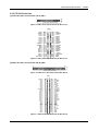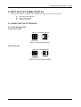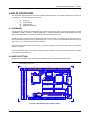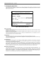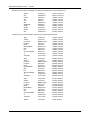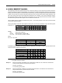
1
AR-B1375/AR-B1376
Half Size All-In-One
386SX CPU CARD
User’ s Guide
Edition: 1.51
Book Number: AR-B1375/AR-B1376-05.0517
AR-B1375/AR-B1376 User’s Guide
Table of Contents
0.
PREFACE...............................................................................................................................................................0-3
0.1
0.2
0.3
0.4
0.5
0.6
0.7
1.
OVERVIEW.............................................................................................................................................................1-1
1.1
1.2
1.3
2.
COPYRIGHT NOTICE AND DISCLAIMER............................................................................................................................ 0-3
WELCOME TO THE AR-B1375/AR-B1376 CPU BOARD ..................................................................................................... 0-3
BEFORE YOU USE THIS GUIDE.......................................................................................................................................... 0-3
RETURNING YOUR BOARD FOR SERVICE ....................................................................................................................... 0-3
TECHNICAL SUPPORT AND USER COMMENTS ............................................................................................................... 0-3
ORGANIZATION .................................................................................................................................................................... 0-4
STATIC ELECTRICITY PRECAUTIONS ............................................................................................................................... 0-4
INTRODUCTION.................................................................................................................................................................... 1-1
PACKING LIST....................................................................................................................................................................... 1-1
FEATURES ............................................................................................................................................................................ 1-2
SYSTEM CONTROLLER .......................................................................................................................................2-1
2.1
MICROPROCESSOR ............................................................................................................................................................ 2-1
2.2
DMA CONTROLLER.............................................................................................................................................................. 2-1
2.3
KEYBOARD CONTROLLER.................................................................................................................................................. 2-2
2.4
INTERRUPT CONTROLLER ................................................................................................................................................. 2-2
2.4.1
I/O Port Address Map..................................................................................................................................................... 2-3
2.4.2
I/O Channel Pin Assignment (Bus1) .............................................................................................................................. 2-3
2.5
REAL-TIME CLOCK AND NON-VOLATILE RAM.................................................................................................................. 2-5
2.6
TIMER .................................................................................................................................................................................... 2-5
2.7
SERIAL PORT........................................................................................................................................................................ 2-6
2.8
PARALLEL PORT .................................................................................................................................................................. 2-8
3.
SETTING UP THE SYSTEM...................................................................................................................................3-1
3.1
OVERVIEW ............................................................................................................................................................................ 3-1
3.2
SYSTEM SETTING ................................................................................................................................................................ 3-2
3.2.1
Keyboard Connector ...................................................................................................................................................... 3-2
3.2.2
PC/104 Connector.......................................................................................................................................................... 3-3
3.2.3
Hard Disk (IDE) Connector (CN4) .................................................................................................................................. 3-5
3.2.4
FDD Port Connector (CN5) ............................................................................................................................................ 3-6
3.2.5
Parallel Port Connector (CN6) ....................................................................................................................................... 3-6
3.2.6
Serial Port....................................................................................................................................................................... 3-7
3.2.7
Reset Header (J1) .......................................................................................................................................................... 3-8
3.2.8
LED Header.................................................................................................................................................................... 3-8
3.2.9
Power Connector (J3) .................................................................................................................................................... 3-9
3.2.10
External Speaker Header (J5).................................................................................................................................... 3-9
3.2.11
External Battery.......................................................................................................................................................... 3-9
3.2.12
CPU Base Clock Select (JP1) .............................................................................................................................................. 3-10
3.2.13
DRAM Configuration ................................................................................................................................................ 3-10
4.
CRT/LCD FLAT PANEL DISPLAY ........................................................................................................................4-1
4.1
CONNECTING THE CRT MONITOR..................................................................................................................................... 4-1
4.1.1
VGA Setting (JP5) .......................................................................................................................................................... 4-1
4.1.2
CRT Connector (CN13).................................................................................................................................................. 4-2
4.2
LCD FLAT PANEL DISPLAY ................................................................................................................................................. 4-2
4.2.1
Inverter Board Description ............................................................................................................................................. 4-3
4.2.2
LCD Connector............................................................................................................................................................... 4-3
4.3
SUPPORTED LCD PANEL .................................................................................................................................................... 4-4
5.
INSTALLATION......................................................................................................................................................5-1
5.1
OVERVIEW ............................................................................................................................................................................ 5-1
5.2
UTILITY DISKETTE ............................................................................................................................................................... 5-1
5.2.1
VGA Driver ..................................................................................................................................................................... 5-2
5.2.2
SSD Utility ...................................................................................................................................................................... 5-3
5.3
WRITE PROTECT FUNCTION .............................................................................................................................................. 5-5
5.3.1
Hardware Write Protect .................................................................................................................................................. 5-6
5.3.2
Software Write Protect ................................................................................................................................................... 5-6
5.3.3
Enable the Software Write Protect ................................................................................................................................. 5-6
5.3.4
Disable the Software Write Protect ................................................................................................................................ 5-6
5.4
WATCHDOG TIMER.............................................................................................................................................................. 5-7
5.4.1
Watchdog Timer Setting................................................................................................................................................. 5-7
5.4.2
Watchdog Timer Enabled............................................................................................................................................... 5-8
5.4.3
Watchdog Timer Trigger................................................................................................................................................. 5-8
5.4.4
Watchdog Timer Disabled .............................................................................................................................................. 5-8
6.
SOLID STATE DISK...............................................................................................................................................6-1
6.1
OVERVIEW ............................................................................................................................................................................ 6-1
0-1
AR-B1375/AR-B1376 User’s Guide
6.2
SWITCH SETTING................................................................................................................................................................. 6-1
6.2.1
Overview ........................................................................................................................................................................ 6-2
6.2.2
I/O Port Address Select (SW1-1) ................................................................................................................................... 6-2
6.2.3
SSD Firmware Address Select (SW1-2) ........................................................................................................................ 6-2
6.2.4
SSD Drive Number (SW1-3 & SW1-4) ........................................................................................................................... 6-3
6.2.5
ROM Type Select (SW1-5 & SW1-6) ............................................................................................................................. 6-4
6.3
JUMPER SETTING ................................................................................................................................................................ 6-5
6.4
ROM DISK INSTALLATION ................................................................................................................................................... 6-6
6.4.1
UV EPROM (27Cxxx)..................................................................................................................................................... 6-6
6.4.2
Large Page 5V FLASH Disk........................................................................................................................................... 6-7
6.4.3
Small Page 5V FLASH ROM Disk ................................................................................................................................. 6-9
6.4.4
RAM Disk ..................................................................................................................................................................... 6-10
6.4.5
Combination of ROM and RAM Disk............................................................................................................................ 6-11
7.
BIOS CONSOLE ....................................................................................................................................................7-1
7.1
BIOS SETUP OVERVIEW ..................................................................................................................................................... 7-1
7.2
STANDARD CMOS SETUP................................................................................................................................................... 7-2
7.3
ADVANCED CMOS SETUP................................................................................................................................................... 7-3
7.4
ADVANCED CHIPSET SETUP.............................................................................................................................................. 7-5
7.5
PASSWORD SETTING.......................................................................................................................................................... 7-6
7.5.1
Setting Password ........................................................................................................................................................... 7-6
7.5.2
Password Checking........................................................................................................................................................ 7-6
7.6
LOAD DEFAULT SETTING.................................................................................................................................................... 7-6
7.6.1
Auto Configuration with Optimal Setting ........................................................................................................................ 7-6
7.6.2
Auto Configuration with Fail Safe Setting....................................................................................................................... 7-7
7.7
BIOS EXIT.............................................................................................................................................................................. 7-7
7.7.1
Save Settings and Exit ................................................................................................................................................... 7-7
7.7.2
Exit Without Saving ........................................................................................................................................................ 7-7
7.8
BIOS UPDATE ....................................................................................................................................................................... 7-7
8.
SPECIFICATIONS & SSD TYPES SUPPORTED ..................................................................................................8-1
8.1
8.2
SPECIFICATIONS ................................................................................................................................................................. 8-1
SSD TYPES SUPPORTED.................................................................................................................................................... 8-1
9. USING MEMORY BANKS......................................................................................................................................9-1
10.
PLACEMENT & DIMENSIONS.........................................................................................................................10-1
10.1
10.2
11.
11.1
11.2
0-2
PLACEMENT ................................................................................................................................................................... 10-1
DIMENSIONS................................................................................................................................................................... 10-2
PROGRAMMING RS-485 & INDEX..................................................................................................................11-1
PROGRAMMING RS-485 ................................................................................................................................................ 11-1
INDEX .............................................................................................................................................................................. 11-3
AR-B1375/AR-B1376 User’s Guide
0.PREFACE
0.1 COPYRIGHT NOTICE AND DISCLAIMER
September 1997
This document is copyrighted, 1997, by Acrosser Technology Co., Ltd. All rights are reserved. No part of this
manual may be reproduced, copied, transcribed, stored in a retrieval system, or translated into any language in
any form or by any means, such as electronic, mechanical, magnetic, optical, chemical, manual or other means
without prior written permission of original manufacturer.
Acrosser Technology assumes no responsibility or warranty with respect to the contents in this manual and
specifically disclaims any implied warranties of merchantability or fitness for any particular purpose. Furthermore,
Acrosser Technology reserves the right to make improvements to the products described in this manual at any
times without notice. Such revisions will be posted on the Internet (WWW.ACROSSER.COM) as soon as possible.
Possession, use, or copying of the software described in this publication is authorized only pursuant to a valid
written license from Acrosser or an authorized sub licensor.
ACKNOWLEDGEMENTS
(C) Copyright Acrosser Technology Co., Ltd., 1997. All rights Reserved.
Acrosser, ALI, AMI, PC/AT, WIN31, WIN 95, Windows NT, NEC, HITACHI, ORION, SHARP, FUJITSU, SONY, AKM,
INTEL, MITSUBISHI, NS, SGS-THOMSON, TI, TOSHIBA, AMD…are registered trademarks.
All other trademarks and registered trademarks are the property of their respective holders.
This document was produced with Adobe Acrobat 3.01.
0.2 WELCOME TO THE AR-B1375/AR-B1376 CPU BOARD
This guide introduces the Acrosser AR-B1375/AR-B1376 CPU board.
The information provided in this manual describes this card’s functions, and features. It also helps you start, set
up and operate your AR-B1375/AR-B1376. General system information can also be found in this publication.
0.3 BEFORE YOU USE THIS GUIDE
Please refer to the Chapter 3, “Setting Up the System” in this guide, if you have not already installed ARB1375/AR-B1376,. Check the packing list before you install and make sure the accessories in the package.
The AR-B1375 & AR-B1376 diskette provides the newest information regarding the CPU card. Please refer to
the README.DOC file of the enclosed utility diskette. It contains the modification and hardware & software
information, and it has updated to product functions that may not be mentioned here..
0.4 RETURNING YOUR BOARD FOR SERVICE
If your board requires any services, contact the distributor or sales representative from whom you purchased the
product for service information. If you need to ship your board to us for service, be sure it is packed in a protective
carton. We recommend that you keep the original shipping container for this purpose.
You can help assure efficient servicing for your product by following these guidelines:
1.
Include your name, address, telephone and facsimile number where you may be reached during the day.
2.
A description of the system configuration and/or software at the time is malfunction.
3.
A brief description of problem occurred.
0.5 TECHNICAL SUPPORT AND USER COMMENTS
User’s comments are always welcome as they assist us in improving the quality of our products and the
readability of our publications. They create a very important part of the input used for product enhancement and
revision.
We may use and distribute any of the information you provide in any way appropriate without incurring any
obligation. You may, of course, continue to use the information you provide.
If you have any suggestions for improving particular sections or if you find any errors, please send your
comments to Acrosser Technology Co., Ltd. or your local sales representative and indicate the manual title and
book number.
Internet electronic mail to: [email protected]
0-3
AR-B1375/AR-B1376 User’s Guide
0.6 ORGANIZATION
This information for users covers the following topics (see the Table of Contents for a detailed listing):
z
z
z
z
z
z
z
z
z
z
z
Chapter 1, “Overview,” provides an overview of the system features and packing list.
Chapter 2, “System Controller,” describes the major structure.
Chapter 3, “Setting Up the System,” describes how to adjust the jumper, and the connectors setting.
Chapter 4, “CRT/LCD Flat Panel Display”, describes the configuration and installation procedure using
LCD and CRT display.
Chapter 5, “Installation,” describes the utility diskette using, solid-state disk’s writing protect function, and
the watchdog timer.
Chapter 6, “Solid State Disk,” describes the various type SSD’s installation steps.
Chapter 7, “BIOS Console,” providing the BIOS options setting.
Chapter 8, Specifications & SSD Types Supported
Chapter 9, Using Memory Banks
Chapter 10, Placement & Dimensions
Chapter 11, Programming RS-485 & Index
0.7 STATIC ELECTRICITY PRECAUTIONS
Before removing the board from its anti-static bag, read this section about static electricity precautions.
Static electricity is a constant danger to computer systems. The charge that can build up in your body may be
more than sufficient to damage integrated circuits on any PC board. It is, therefore, important to observe basic
precautions whenever you use or handle computer components. Although areas with humid climates are much
less prone to static build-up, it is always best to safeguard against accidents may result in expensive repairs. The
following measures should generally be sufficient to protect your equipment from static discharge:
•
•
•
0-4
Touch a grounded metal object to discharge the static electricity in your body (or ideally, wear a grounded
wrist strap).
When unpacking and handling the board or other system component, place all materials on an antic static
surface.
Be careful not to touch the components on the board, especially the “golden finger” connectors on the bottom
of every board.
AR-B1375/AR-B1376 User’s Guide
1. OVERVIEW
This chapter provides an overview of your system features and capabilities. The following topics are covered:
z
z
z
Introduction
Packing List
Features
1.1 INTRODUCTION
The AR-B1375 and AR-B1376 are new generation half size, 386 ISA card. This card offers much greater performance
than the older cards such as support for 32MB’s of DRAM using two 72-pin SIMMs, one RS-232C/485 and one RS-232C
port and 3/1.5MB solid state disk capacity for ROM, FLASH and SRAM.
The unit also comes with a programmable watchdog timer and other typical interfaces. These 386 CPU cards are excellent
for embedded systems, MMI’s, workstations, medical applications or POS/POI systems. As well, an RS-232C/485 port
provided remote control. RS-485 has not been offered until recently on 386 cards.
Especially the AR-B1376 with on board VGA, offers the most exciting possibilities yet to the industry. The on board
VGA/LCD controller brings about a whole new dimension of industrial computing. No longer do you have to worry about
adding an extra card to your system. Negating the need of a separate VGA card saves space. The VGA/LCD unit comes
with 1MB of V-RAM on board and uses the C&T 65545 Chipset, to support a wide range of LCD Panels.
1.2 PACKING LIST
The accessories are included with the system. Before you begin installing your AR-B1375 or AR-B1376 board,
take a moment to make sure that the following items have been included inside the AR-B1375 or AR-B1376
package.
z
z
z
z
z
z
z
The quick setup manual
1 AR-B1375 or AR-B1376 all-in-one single CPU board
1 Hard disk drive interface cable
1 Floppy disk drive interface cable
1 Parallel port interface cable
1 RS-232C interface cable
2 Software utility CD (AR-B1375 has not the VGA function, and only encloses one SSD utility
diskette).
1-1
AR-B1375/AR-B1376 User’s Guide
1.3 FEATURES
The system provides a number of special features that enhance its reliability, ensure its availability, and improve its
expansion capabilities, as well as its hardware structure.
z
z
z
z
z
z
z
z
z
z
z
z
z
z
z
z
1-2
80386SX-33/40 MHz CPU
ISA and PC/104 extension bus
Up to 32MB DRAM system
On-board CRT and LCD panel display (AR-B1375 doesn’t provide this function)
Supports IDE hard disk drives
Supports floppy disk drives
Supports 1 bi-directional parallel port
Supports 2 serial ports (RS-232C and RS-485)
PC/AT compatible keyboard
Up to 3MB solid state disk
Programmable watchdog timer
Flash BIOS
Built-in status LEDs indicator
Signal 5V power requirement
Multi-layer PCB for noise reduction
Dimensions: 185mmX122mm
AR-B1375/AR-B1376 User’s Guide
2. SYSTEM CONTROLLER
This chapter describes the major structure of the AR-B1375 and AR-B1376 CPU board. The following topics are
covered:
z
z
z
z
z
z
z
z
Microprocessor
DMA Controller
Keyboard Controller
Interrupt Controller
Real-Time Clock and Non-Volatile RAM
Timer
Serial Port
Parallel Port
2.1 MICROPROCESSOR
The AR-B1375 and AR-B1376 use the ALI M6117 CPU, it is designed to perform like Intel’s 386SX system with
deep green features.
The 386SX core is the same as M1386SX of Acer Labs. Inc. and 100% object code compatible with the Intel
386SX microprocessor. System manufacturers can provide 386 CPU based systems optimized for both cost and
size. Instruction pipelining and high bus bandwidth ensure short average instruction execution times and high
system throughput. Furthermore, it can keep the state internally from charge leakage while external clock to the
core is stopped without storing the data in registers. The power consumption here is almost zero when clock stops.
The internal structure of this core is 32-bit data and address bus with very low supply current. Real mode as well
as Protected mode are available and can run MS-DOS, MS-Windows, OS/2 and UNIX.
2.2 DMA CONTROLLER
The equivalent of two 8237A DMA controllers are implemented in the AR-B1375/AR-B1376 board. Each controller
is a four-channel DMA device that will generate the memory addresses and control signals necessary to transfer
information directly between a peripheral device and memory. This allows high speeding information transfer with less
CPU intervention. The two DMA controllers are internally cascaded to provide four DMA channels for transfers to
8-bit peripherals (DMA1) and three channels for transfers to 16-bit peripherals (DMA2). DMA2 channel 0 provides
the cascade interconnection between the two DMA devices, thereby maintaining IBM PC/AT compatibility.
Following is the system information of DMA channels:
DMA Controller 1
DMA Controller 2
Channel 0: Spare
Channel 4: Cascade for controller 1
Channel 1: IBM SDLC
Channel 5: Spare
Channel 2: Diskette adapter
Channel 6: Spare
Channel 3: Spare
Channel 7: Spare
Table 2-1 DMA Channel Controller
2-1
AR-B1375/AR-B1376 User’s Guide
2.3 KEYBOARD CONTROLLER
The 8042 processor is programmed to support the keyboard serial interface. The keyboard controller receives
serial data from the keyboard, checks its parity, translates scan codes, and presents it to the system as a byte data
in its output buffer. The controller can interrupt the system when data is placed in its output buffer, or wait for the
system to poll its status register to determine when data is available.
Data can be written to the keyboard by writing data to the output buffer of the keyboard controller.
Each byte of data is sent to the keyboard controller in series with an odd parity bit automatically inserted. The
keyboard controller is required to acknowledge all data transmissions. Therefore, another byte of data will not be
sent to keyboard controller until acknowledgment is received for the previous byte sent. The “output buffer full”
interruption may be used for both send and receive routines.
2.4 INTERRUPT CONTROLLER
The equivalent of two 8259 Programmable Interrupt Controllers (PIC) are included on the AR-B1375/AR-B1376
board. They accept requests from peripherals, resolve priorities on pending interrupts in service, issue interrupt
requests to the CPU, and provide vectors which are used as acceptance indices by the CPU to determine which
interrupt service routine to execute.
Following is the system information of interrupt levels:
Interrupt Level
In
Description
NMI
Parity check
CTRL1
IRQ 0
IRQ 1
IRQ 2
CTRL2
System timer interrupt from timer 8254
Keyboard output buffer full
IRQ8 : Real time clock
IRQ9 : Rerouting to INT 0Ah from hardware IRQ2
IRQ10 : Spare
IRQ11 : Spare
IRQ12 : Spare
IRQ13 : Math. coprocessor
IRQ14 : Hard disk adapter
IRQ15 : Reserved for watchdog
IRQ 3
IRQ 4
IRQ 5
IRQ 6
IRQ 7
Serial port 2
Serial port 1
Parallel port 2
Floppy disk adapter
Parallel port 1
Figure 2-1 Interrupt Controller
2-2
AR-B1375/AR-B1376 User’s Guide
2.4.1 I/O Port Address Map
Hex Range
Device
000-01F
DMA controller 1
020-021
Interrupt controller 1
022-023
ALI M6117
040-04F
Timer 1
050-05F
Timer 2
060-06F
8042 keyboard/controller
070-071
Real-time clock (RTC), non-maskable interrupt (NMI)
080-09F
DMA page registers
0A0-0A1
Interrupt controller 2
0C0-0DF
DMA controller 2
0F0
Clear Math Co-processor
0F1
Reset Math Co-processor
0F8-0FF
Math Co-processor
170-178
Fixed disk 1
1F0-1F8
Fixed disk 0
201
Game port
208-20A
EMS register 0
218-21A
EMS register 1
278-27F
Parallel printer port 2 (LPT 2)
2E8-2EF
Serial port 4 (COM 4)
2F8-2FF
Serial port 2 (COM 2)
300-31F
Prototype card/streaming type adapter
320-33F
LAN adapter
378-37F
Parallel printer port 1 (LPT 1)
380-38F
SDLC, bisynchronous
3A0-3AF
Bisynchronous
3B0-3BF
Monochrome display and printer port 3 (LPT 3)
3C0-3CF
EGA/VGA adapter
3D0-3DF
Color/graphics monitor adapter
3E8-3EF
Serial port 3 (COM 3)
3F0-3F7
Diskette controller
3F8-3FF
Serial port 1 (COM 1)
Table 2-2 I/O Port Address Map
2.4.2 I/O Channel Pin Assignment (Bus 1)
I/O Pin
Signal Name
A1
-IOCHCK
Input/Output I/O Pin Signal Name
Input
B1
GND
Input/Output
Ground
A2
SD7
Input/Output
B2
RSTDRV
Output
A3
SD6
Input/Output
B3
+5V
Power
A4
SD5
Input/Output
B4
IRQ9
Input
A5
SD4
Input/Output
B5
-5V
Power
A6
SD3
Input/Output
B6
DRQ2
Input
A7
SD2
Input/Output
B7
-12V
Power
A8
SD1
Input/Output
B8
-ZWS
Input
A9
SD0
Input/Output
B9
+12V
Power
A10
IOCHRDY
Input
B10
GND
Ground
A11
AEN
Output
B11
-SMEMW
Output
A12
SA19
Input/Output
B12
-SMEMR
Output
A13
SA18
Input/Output
B13
-IOW
Input/Output
A14
SA17
Input/Output
B14
-IOR
Input/Output
A15
SA16
Input/Output
B15
-DACK3
Output
A16
SA15
Input/Output
B16
DRQ3
Input
2-3
AR-B1375/AR-B1376 User’s Guide
I/O Pin
Signal Name
A17
SA14
Input/Output I/O Pin Signal Name
Input/Output
B17
A18
SA13
Input/Output
B18
DRQ1
Input
A19
SA12
Input/Output
B19
-REFRESH
Input/Output
-DACK1
Input/Output
Output
A20
SA11
Input/Output
B20
BUSCLK
Output
A21
SA10
Input/Output
B21
IRQ7
Input
A22
SA9
Input/Output
B22
IRQ6
Input
A23
SA8
Input/Output
B23
IRQ5
Input
A24
SA7
Input/Output
B24
IRQ4
Input
A25
SA6
Input/Output
B25
IRQ3
Input
A26
SA5
Input/Output
B26
-DACK2
Output
A27
SA4
Input/Output
B27
TC
Output
A28
SA3
Input/Output
B28
BALE
Output
A29
SA2
Input/Output
B29
+5V
Power
A30
SA1
Input/Output
B30
OSC
Output
A31
SA0
Input/Output
B31
GND
Ground
Table 2-3 I/O Channel Pin Assignments
I/O Pin Signal Name
Input/Output
I/O Pin
Signal Name
Input/Output
C1
-SBHE
Input/Output
D1
-MEMCS16
Input
C2
LA23
Input/Output
D2
-IOCS16
Input
C3
LA22
Input/Output
D3
IRQ10
Input
C4
LA21
Input/Output
D4
IRQ11
Input
C5
LA20
Input/Output
D5
IRQ12
Input
C6
LA19
Input/Output
D6
IRQ15
Input
C7
LA18
Input/Output
D7
IRQ14
Input
C8
LA17
Input/Output
D8
-DACK0
Output
C9
-MRD16
Input/Output
D9
DRQ0
Input
C10
-MWR16
Input/Output
D10
-DACK5
Output
C11
SD8
Input/Output
D11
DRQ5
Input
C12
SD9
Input/Output
D12
-DACK6
Output
C13
SD10
Input/Output
D13
DRQ6
Input
Output
C14
SD11
Input/Output
D14
-DACK7
C15
SD12
Input/Output
D15
DRQ7
Input
C16
SD13
Input/Output
D16
+5V
Power
C17
SD14
Input/Output
D17
-MASTER
Input
C18
SD15
Input/Output
D18
GND
Ground
Table 2-4 I/O Channel Pin Assignments
2-4
AR-B1375/AR-B1376 User’s Guide
2.5 REAL-TIME CLOCK AND NON-VOLATILE RAM
The AR-B1375/AR-B1376 contains a real-time clock compartment that maintains the date and time in addition to
storing configuration information about the computer system. It contains 14 bytes of clock and control registers
and 114 bytes of general purpose RAM. Because of the use of CMOS technology, it consumes very little power
and can be maintained for long period of time using an internal Lithium battery. The contents of each byte in the
CMOS RAM are listed as follows:
Address
Description
00
Seconds
01
Second alarm
02
Minutes
03
Minute alarm
04
Hours
05
Hour alarm
06
Day of week
07
Date of month
08
Month
09
Year
0A
Status register A
0B
Status register B
0C
Status register C
0D
Status register D
0E
Diagnostic status byte
0F
Shutdown status byte
10
Diskette drive type byte, drive A and B
11
Fixed disk type byte, drive C
12
Fixed disk type byte, drive D
13
Reserved
14
Equipment byte
15
Low base memory byte
16
High base memory byte
17
Low expansion memory byte
18
High expansion memory byte
19-2D
Reserved
2E-2F
2-byte CMOS checksum
30
Low actual expansion memory byte
31
High actual expansion memory byte
32
Date century byte
33
Information flags (set during power on)
34-7F
Reserved for system BIOS
Table 2-5 Real-Time Clock & Non-Volatile RAM
2.6 TIMER
The AR-B1375/AR-B1376 provides three programmable timers, each with a timing frequency of 1.19 MHz.
Timer 0
The output of this timer is tied to interrupt request 0. (IRQ 0)
Timer 1
This timer is used to trigger memory refresh cycles.
Timer 2
This timer provides the speaker tone.
Application programs can load different counts into this timer to generate various sound frequencies.
2-5
AR-B1375/AR-B1376 User’s Guide
2.7 SERIAL PORT
The ACEs (Asynchronous Communication Elements ACE1 to ACE4) are used to convert parallel data to a serial
format on the transmit side and convert serial data to parallel on the receiver side. The serial format, in order of
transmission and reception, is a start bit, followed by five to eight data bits, a parity bit (if programmed) and one,
one and half (five-bit format only) or two stop bits. The ACEs are capable of handling divisors of 1 to 65535, and
produce a 16x clock for driving the internal transmitter logic.
Provisions are also included to use this 16x clock to drive the receiver logic. Also included in the ACE a completed
MODEM control capability, and a processor interrupt system that may be software tailored to the computing time
required handle the communications link.
The following table is summary of each ACE accessible register
DLAB
0
Port Address
base + 0
Register
Receiver buffer (read)
Transmitter holding register (write)
0
base + 1
Interrupt enable
X
base + 2
Interrupt identification (read only)
X
base + 3
Line control
X
base + 4
MODEM control
X
base + 5
Line status
X
base + 6
MODEM status
X
base + 7
Scratched register
1
base + 0
Divisor latch (least significant byte)
1
base + 1
Divisor latch (most significant byte)
Table 2-6 ACE Accessible Registers
(1) Receiver Buffer Register (RBR)
Bit 0-7: Received data byte (Read Only)
(2) Transmitter Holding Register (THR)
Bit 0-7: Transmitter holding data byte (Write Only)
(3) Interrupt Enable Register (IER)
Bit 0: Enable Received Data Available Interrupt (ERBFI)
Bit 1: Enable Transmitter Holding Empty Interrupt (ETBEI)
Bit 2: Enable Receiver Line Status Interrupt (ELSI)
Bit 3: Enable MODEM Status Interrupt (EDSSI)
Bit 4: Must be 0
Bit 5: Must be 0
Bit 6: Must be 0
Bit 7: Must be 0
(4) Interrupt Identification Register (IIR)
Bit 0: “0” if Interrupt Pending
Bit 1: Interrupt ID Bit 0
Bit 2: Interrupt ID Bit 1
Bit 3: Must be 0
Bit 4: Must be 0
Bit 5: Must be 0
Bit 6: Must be 0
Bit 7: Must be 0
2-6
AR-B1375/AR-B1376 User’s Guide
(5) Line Control Register (LCR)
Bit 0: Word Length Select Bit 0 (WLS0)
Bit 1: Word Length Select Bit 1 (WLS1)
WLS1
WLS0
Word Length
0
0
5 Bits
0
1
6 Bits
1
0
7 Bits
1
1
8 Bits
Bit 2: Number of Stop Bit (STB)
Bit 3: Parity Enable (PEN)
Bit 4: Even Parity Select (EPS)
Bit 5: Stick Parity
Bit 6: Set Break
Bit 7: Divisor Latch Access Bit (DLAB)
(6) MODEM Control Register (MCR)
Bit 0: Data Terminal Ready (DTR)
Bit 1: Request to Send (RTS)
Bit 2: Out 1 (OUT 1)
Bit 3: Out 2 (OUT 2)
Bit 4: Loop
Bit 5: Must be 0
Bit 6: Must be 0
Bit 7: Must be 0
(7) Line Status Register (LSR)
Bit 0: Data Ready (DR)
Bit 1: Overrun Error (OR)
Bit 2: Parity Error (PE)
Bit 3: Framing Error (FE)
Bit 4: Break Interrupt (BI)
Bit 5: Transmitter Holding Register Empty (THRE)
Bit 6: Transmitter Shift Register Empty (TSRE)
Bit 7: Must be 0
(8) MODEM Status Register (MSR)
Bit 0: Delta Clear to Send (DCTS)
Bit 1: Delta Data Set Ready (DDSR)
Bit 2: Training Edge Ring Indicator (TERI)
Bit 3: Delta Receive Line Signal Detect (DSLSD)
Bit 4: Clear to Send (CTS)
Bit 5: Data Set Ready (DSR)
Bit 6: Ring Indicator (RI)
Bit 7: Received Line Signal Detect (RSLD)
2-7
AR-B1375/AR-B1376 User’s Guide
(9) Divisor Latch (LS, MS)
LS
Bit 0
Bit 1
Bit 2
Bit 3
Bit 4
Bit 5
Bit 6
Bit 7
Bit 0:
Bit 1:
Bit 2:
Bit 3:
Bit 4:
Bit 5:
Bit 6:
Bit 7:
MS
Bit 8
Bit 9
Bit 10
Bit 11
Bit 12
Bit 13
Bit 14
Bit 15
Desired
Divisor Used to
Baud Rate Generate 16x Clock
50
2304
75
1536
110
1047
134.5
857
150
768
300
384
600
192
1200
96
1800
64
2000
58
2400
48
3600
32
4800
24
7200
16
9600
12
14400
8
19200
6
28800
4
38400
3
57600
2
Table 2-7 Serial Port Divisor Latch
Present Error Difference
Between Desired and Actual
----0.026
0.058
----------0.69
---------------------
2.8 PARALLEL PORT
(1) Register Address
Port Address
Read/Write
base + 0
Write
base + 0
Read
base + 1
Read
base + 2
Write
Table 2-8 Registers’ Address
Register
Output data
Input data
Printer status buffer
Printer control latch
(2) Printer Interface Logic
The parallel portion of the SMC37C669 makes the attachment of various devices that accept eight bits of parallel
data at standard TTL level.
(3) Data Swapper
The system microprocessor can read the contents of the printer’s Data Latch through the Data Swapper by reading
the Data Swapper address.
2-8
AR-B1375/AR-B1376 User’s Guide
(4) Printer Status Buffer
The system microprocessor can read the printer status by reading the address of the Printer Status Buffer. The bit
definitions are described as follows:
7
6
5
4
3
2
1
0
X
X
X
-ERROR
SLCT
PE
-ACK
-BUSY
Figure 2-2 Printer Status Buffer
NOTE: X presents not used.
Bit 7: This signal may become active during data entry, when the printer is off-line during printing, or when the
print head is changing position or in an error state. When Bit 7 is active, the printer is busy and cannot
accept data.
Bit 6: This bit represents the current state of the printer’s ACK signal. A0 means the printer has received the
character and is ready to accept another. Normally, this signal will be active for approximately 5
microseconds before receiving a BUSY message stops.
Bit 5: A1 means the printer has detected the end of the paper.
Bit 4: A1 means the printer is selected.
Bit 3: A0 means the printer has encountered an error condition.
(5) Printer Control Latch & Printer Control Swapper
The system microprocessor can read the contents of the printer control latch by reading the address of printer
control swapper. Bit definitions are as follows:
7
6
X
X
5
4
3
2
1
0
STROBE
AUTO FD XT
INIT
SLDC IN
IRQ ENABLE
DIR(write only)
Figure 2-3 Bit’s Definition
NOTE: X presents not used.
Bit 5: Direction control bit. When logic 1, the output buffers in the parallel port are disabled allowing data driven
from external sources to be read; when logic 0, they work as a printer port. This bit is write only.
Bit 4: A1 in this position allows an interrupt to occur when ACK changes from low state to high state.
Bit 3: A1 in this bit position selects the printer.
Bit 2: A0 starts the printer (50 microseconds pulse, minimum).
Bit 1: A1 causes the printer to line-feed after a line is printed.
Bit 0: A0.5 microsecond minimum highly active pulse clocks data into the printer. Valid data must be present for
a minimum of 0.5 microseconds before and after the strobe pulse.
2-9
AR-B1375/AR-B1376 User’s Guide
3. SETTING UP THE SYSTEM
This section describes pin assignments for system’s external connectors and the jumpers setting.
Overview
System Setting
z
z
3.1 OVERVIEW
The AR-B1375 and AR-B1376 are all-in-one half size, Pentium single CPU board.
hardware’s jumpers setting, the connectors’ locations, and the pin assignment.
This section provides
CAUTION: The CPU board doesn’t support the type DRAM SIMM of two-sided, it only supports single side DRAM
SIMM.
J11
J1 J8
CN4
CN5
CN6
H4
H9
1
1
J6
P2
P1
P5
P3H5
P4
P6
CN8
U12
105
JP6
1
H6
1
104
31
81
J9
1
CN7
LED2
100
1
JP7
JP4
LED1
CN9
1
2
J3
J2
1
50
51
M1
SIMM1
SIMM2
U3
1
2
3
A B C
1
2
3
A B C
1
2
3
A B C
M3
U34
M2
MEM1
U31
105
1
104
H10 BUS2
H11
LED3
JP3
J5
1
DB1
JP5
2
1
1
JP1
JP2
SW1
U32
MEM2
U10
U33
MEM3
U11
J7
J10
1
DB2
J4
CN2
CN1
H8
BUS1
H7
CN1
1
2
1
CN3
Figure 3-1 AR-B1376 Jumpers & Connectors Placement
3-1
1
1
AR-B1375/AR-B1376 User’s Guide
3.2 SYSTEM SETTING
Jumper pins allow you to set specific system parameters. Set them by changing the pin location of jumper blocks.
(A jumper block is a small plastic-encased conductor [shorting plug] that slips over the pins.) To change a jumper
setting, remove the jumper from its current location with your fingers or small needle-nosed pliers. Place the
jumper over the two pins designated for the desired setting. Press the jumper evenly onto the pins. Be careful not
to bend the pins.
We will show the locations of the AR-B1375 and AR-B1376 jumper pins, and the factory-default setting.
CAUTION: Do not touch any electronic component unless you are safely grounded. Wear a grounded wrist strap
or touch an exposed metal part of the system unit chassis. The static discharges from your fingers can
permanently damage electronic components.
3.2.1 Keyboard Connector
(1) 6-Pin Mini DIN Keyboard Connector (CN3)
CN3 is a Mini-DIN 6-pin connector. This keyboard connector is PS/2 type keyboard connector. This connector is
also for a standard IBM-compatible keyboard with the keyboard adapter cable.
1
2
3
4
5
6
CN3
DATA
1 2
N.C.
3
4
GND
VCC
6
5
CLOCK
Front View
N.C.
Figure 3-2 CN3: 6-Pin Mini Din Keyboard Connector
(2) AUX. Keyboard Connector (J4)
We can use a PC/AT compatible keyboard to connecting the provided adapter cable between J4 and the keyboard.
The pin assignments of J4 connector are as follows:
1
2
3
4
5
J4
CLOCK
DATA
N.C.
GND
VCC
Figure 3-3 J4: AUX. Keyboard Connector
3-2
AR-B1375/AR-B1376 User’s Guide
3.2.2 PC/104 Connector
(1) 40-Pin PC/104 Connector Bus C & D (CN1)
1
2
39
40
40 Pin PC/104 Connector
Figure 3-4 CN1: 40-Pin PC/104 Connector Bus C & D
CN1
1
GND ---SBHE --LA23 --LA22 --LA21 --LA20 --LA19 --LA18 --LA17 ---MEMR ---MEMW --SD8 --SD9 --SD10 --SD11 --SD12 --SD13 --SD14 --SD15 --Not Used ---
2
C1
C2
C3
C4
C5
C6
C7
C8
C9
C10
C11
C12
C13
C14
C15
C16
C17
C18
C19
C20
D1
D2
D3
D4
D5
D6
D7
D8
D9
D10
D11
D12
D13
D14
D15
D16
D17
D18
D19
D20
--- GND
--- -MEM16
--- -IO16
--- IRQ10
--- IRQ11
--- IRQ12
--- IRQ15
--- IRQ14
--- -DACK0
--- DRQ0
--- -DACK5
--- DRQ5
--- -DACK6
--- DRQ6
--- -DACK7
--- DRQ7
--- +5 VDC
--- -MASTER
--- GND
--- GND
Figure 3-5 CN1: 40-Pin PC/104 Connector Bus C & D
(2) 64-Pin PC/104 Connector Bus A & B (CN2)
64
2
1
64-Pin PC/104 Connector
63
Figure 3-6 CN2: 64 Pin PC/104 Connector Bus A & B
-IOCHCK --SD7 --SD6 --SD5 --SD4 --SD3 --SD2 --SD1 --SD0 --IOCHRDY--AEN --SA19 --SA18 --SA17 --SA16 --SA15 --SA14 --SA13 --SA12 --SA11 --SA10 --SA9 --SA8 --SA7 --SA6 --SA5 --SA4 --SA3 --SA2 --SA1 --SA0 --GND ---
A1
A2
A3
A4
A5
A6
A7
A8
A9
A10
A11
A12
A13
A14
A15
A16
A17
A18
A19
A20
A21
A22
A23
A24
A25
A26
A27
A28
A29
A30
A31
A32
CN2
1 2
B1
B2
B3
B4
B5
B6
B7
B8
B9
B10
B11
B12
B13
B14
B15
B16
B17
B18
B19
B20
B21
B22
B23
B24
B25
B26
B27
B28
B29
B30
B31
B32
--- GND
--- RSTDRV
--- +5 VDC
--- IRQ9
--- -5 VDC
--- DRQ2
--- -12 VDC
--- -ZWS
--- +12 VDC
--- Not Used
--- -SMEMW
--- -SMEMR
--- -IOW
--- -IOR
--- -DACK3
--- DRQ3
--- -DACK1
--- DRQ1
--- -REFRSH
--- BUSCLK
--- IRQ7
--- IRQ6
--- IRQ5
--- IRQ4
--- IRQ3
--- -DACK2
--- TC
--- BALE
--- +5 VDC
--- OSC
--- GND
--- GND
Figure 3-7 CN2: 64-Pin PC/104 Connector Bus A & B
3-3
AR-B1375/AR-B1376 User’s Guide
(3) I/O Channel Signal Description
Name
Description
BUSCLK [Output]
The BUSCLK signal of the I/O channel is asynchronous to
the CPU clock.
RSTDRV [Output]
This signal goes high during power-up, low line-voltage or
hardware reset
The System Address lines run from bit 0 to 19. They are
[Input / Output] latched onto the falling edge of "BALE"
SA0 - SA19
The Unlatched Address line run from bit 17 to 23
LA17 - LA23
[Input/Output]
System Data bit 0 to 15
SD0 - SD15
[Input/Output]
BALE [Output]
The Buffered Address Latch Enable is used to latch SA0 SA19 onto the falling edge. This signal is forced high
during DMA cycles
-IOCHCK [Input]
The I/O Channel Check is an active low signal which
indicates that a parity error exist on the I/O board
This signal lengthens the I/O, or memory read/write cycle,
[Input, Open collector] and should be held low with a valid address
IOCHRDY
The Interrupt Request signal indicates I/O service request
[Input] attention. They are prioritized in the following sequence :
(Highest) IRQ 9, 10, 11, 12, 13, 15, 3, 4, 5, 6, 7 (Lowest)
IRQ 3-7, 9-12, 14, 15
-IOR
The I/O Read signal is an active low signal which instructs
[Input/Output] the I/O device to drive its data onto the data bus
-IOW [Input/Output]
The I/O write signal is an active low signal which instructs
the I/O device to read data from the data bus
-SMEMR [Output]
The System Memory Read is low while any of the low 1
mega bytes of memory are being used
The Memory Read signal is low while any memory location
[Input/Output] is being read
-MEMR
-SMEMW [Output]
The System Memory Write is low while any of the low 1
mega bytes of memory is being written
The Memory Write signal is low while any memory location
[Input/Output] is being written
-MEMW
DRQ 0-3, 5-7 [Input] DMA Request channels 0 to 3 are for 8-bit data transfers.
DMA Request channels 5 to 7 are for 16-bit data transfers.
DMA request should be held high until the corresponding
DMA has been completed. DMA request priority is in the
following sequence:(Highest) DRQ 0, 1, 2, 3, 5, 6, 7
(Lowest)
The DMA Acknowledges 0 to 3, 5 to 7 are the
[Output] corresponding acknowledge signals for DRQ 0 to 3 and 5
to 7
-DACK 0-3, 5-7
AEN [output]
The DMA Address Enable is high when the DMA controller
is driving the address bus. It is low when the CPU is driving
the address bus
This signal is used to indicate a memory refresh cycle and
[Input/Output] can be driven by the microprocessor on the I/O channel
-REFRESH
TC [Output]
Terminal Count provides a pulse when the terminal count
for any DMA channel is reached
SBHE [Input/Output] The System Bus High Enable indicates the high byte SD8 -
SD15 on the data bus
3-4
AR-B1375/AR-B1376 User’s Guide
Name
-MASTER [Input]
Description
The MASTER is the signal from the I/O processor which
gains control as the master and should be held low for a
maximum of 15 microseconds or system memory may be
lost due to the lack of refresh
-MEMCS16
The Memory Chip Select 16 indicates that the present data
[Input, Open collector] transfer is a 1-wait state, 16-bit data memory operation
The I/O Chip Select 16 indicates that the present data
[Input, Open collector] transfer is a 1-wait state, 16-bit data I/O operation
-IOCS16
OSC [Output]
The Oscillator is a 14.31818 MHz signal used for the color
graphic card
-ZWS
The Zero Wait State indicates to the microprocessor that
[Input, Open collector] the present bus cycle can be completed without inserting
additional wait cycle
Table 3-9 I/O Channel Signal’s Description
3.2.3 Hard Disk (IDE) Connector (CN4)
A 40-pin header type connector (CN4) is provided to interface with up to two embedded hard disk drives (IDE AT
bus). This interface, through a 40-pin cable, allows the user to connect up to two drives in a “daisy chain” fashion.
To enable or disable the hard disk controller, please use BIOS Setup program to select. The following table
illustrates the pin assignments of the hard disk drive’s 40-pin connector.
1
2
Figure 3-8 CN4: Hard Disk (IDE) Connector
Pin
Signal
1
-RESET
3
DATA 7
5
DATA 6
7
DATA 5
9
DATA 4
11
DATA 3
13
DATA 2
15
DATA 1
17
DATA 0
19
GROUND
21
NOT USED
23
-IOW
25
-IOR
27
-IORDY
29
NOT USED
31
IRQ 14
33
SA 1
35
SA 0
37
-CS 0
39
HD LED
Table 3-1 HDD Pin Assignment
Pin
2
4
6
8
10
12
14
16
18
20
22
24
26
28
30
32
34
36
38
40
Signal
GROUND
DATA 8
DATA 9
DATA 10
DATA 11
DATA 12
DATA 13
DATA 14
DATA 15
NOT USED
GROUND
GROUND
GROUND
BALE
GROUND
-IOCS16
NOT USED
SA 2
-CS 1
GROUND
3-5
AR-B1375/AR-B1376 User’s Guide
3.2.4 FDD Port Connector (CN5)
The AR-B1375 and AR-B1376 provide a 34-pin header type connector for supporting up to two floppy disk drives.
1
2
Figure 3-9 CN5: FDD Port Connector
Pin
Signal
Pin
Signal
1-33(odd)
GROUND
18
DIRECTION
2
-REDUCED WRITE
CURRENT
20
-STEP OUTPUT PULSE
4
NOT USED
22
-WRITE DATA
6
NOT USED
24
-WRITE ENABLE
8
-INDEX
26
-TRACK 0
10
-MOTOR ENABLE A
28
-WRITE PROTECT
12
-DRIVE SELECT B
30
-READ DATA
14
-DRIVE SELECT A
32
-SIDE 1 SELECT
34
DISK CHANGE
16
-MOTOR ENABLE B
Table 3-1 FDD Pin Assignment
3.2.5 Parallel Port Connector (CN6)
To use the parallel port, an adapter cable has connected to the CN6 (26-pin header type) connector. This adapter
cable is mounted on a bracket and is included in your AR-B1375 or AR-B1376 package. The connector for the
parallel port is a 25 pin D-type female connector.
1
2
Parallel Port Connector
13
25
1
DB-25
D-Type Connector
14
Figure 3-10 CN6: Parallel Port Connector
CN6
DB-25
Signal
CN6
DB-25
Signal
1
1
-Strobe
2
14
-Auto Form Feed
3
2
Data 0
4
15
-Error
5
3
Data 1
6
16
-Initialize
7
4
Data 2
8
17
-Printer Select In
9
5
Data 3
10
18
Ground
11
6
Data 4
12
19
Ground
13
7
Data 5
14
20
Ground
15
8
Data 6
16
21
Ground
17
9
Data 7
18
22
Ground
19
10
-Acknowledge
20
23
Ground
21
11
Busy
22
24
Ground
23
12
Paper
24
25
Ground
--
No Connect
25
13
Printer Select
26
Table 3-1 Parallel Port Pin Assignment
3-6
AR-B1375/AR-B1376 User’s Guide
3.2.6 Serial Port
(1) RS-232/RS-485 Select for COM-B (JP2)
JP2 select the on-board RS-232/RS-485 for COM B, if choose RS-232 connecting with CN7; if choose RS-485
connecting with J9.
JP2
1 2 3
RS-232C
(Factory Preset)
1 2 3
RS-485
Figure 3-11 JP2: RS-232/RS-485 Select for COM-B
(2) RS-485 Terminator (JP7)
JP7
1 2
OFF
Factory Preset
1
2
ON
Figure 3-12 JP7: RS-485 Terminator
(3) External RS-485 Adapter Select (J6 & J7)
J6 and J7 can be set independently. J7 selects COM A port and J6 selects COM A port. J6 selects the external
RS-485 for COM B connecting with CN7. J7 selects the external RS-485 for COM A connecting with DB2.
J6 & J7
1 2 3
External RS-485 Adapter
1 2 3
RS-232C
(Factory Preset)
Figure 3-13 J6 & J7: External RS-485 Adapter Select
(4) RS-485 Header (J9)
J9 is on-board RS-485 header. J9 pin assignments are as follows:
1 N485+
2 N4851 2 3
3 GND
J9 (COM B)
Figure 3-14 J9: RS-485 Header
3-7
AR-B1375/AR-B1376 User’s Guide
(5) RS-232 Connector (CN7 & DB2)
There are two serial ports with EIA RS-232 interface on the AR-B1375 or AR-B1376. COM A uses one on-board
D-type 9-pin male connector (DB2) which is located at the right side of the card, and COM B uses one 10-pin
header (CN7) which is located at the upper of the card. To configure these two serial ports, use the BIOS Setup
program to do well, and adjust the jumpers on J6 and J7.
The pin assignments of the DB2 and CN7 for serial port A & B are as follows:
DB2 (COM A)
CN7 (COM B)
GND 5
-DTR 4
TXD 3
RXD 2
-DCD 1
1
9-RI
2
8-CTS
7-RTS
6-DSR
Figure 3-15 CN7 & DB2: RS-232 Connector
CN7
DB2
Signal
CN7
DB2
Signal
1
1
-DCD
2
6
-DSR
3
2
RXD
4
7
-RTS
5
3
TXD
6
8
-CTS
7
4
-DTR
8
9
-RI
9
5
GND
10
Table 3-2 Serial Port Pin Assignment
--
Not Used
3.2.7 Reset Header (J1)
J1 is used to connect to an external reset switch. Shorting these two pins will reset the system.
1 Reset+
2 ResetFigure 3-16 J1: Reset Header
3.2.8 LED Header
(1) External Power LED Header (J2)
1 2 3
1 Power LED+
2 No Connect
3 Power LED-
Figure 3-17 J2: External Power LED Header
(2) HDD LED Header (J8)
1 LED+
2 LEDFigure 3-18 J8: HDD LED Header
3-8
AR-B1375/AR-B1376 User’s Guide
(3) Watchdog LED Header (J10)
1 LED+
2 LEDFigure 3-19 J10: Watchdog LED Header
3.2.9 Power Connector (J3)
J3 is 8-pin power connector, you can directly connect the power supply to the on board power connector for stand
alone applications.
1
GND
2
+5 VDC
+5 VDC
GND
GND
+12 VDC
-12 VDC
-5 VDC
3
4
5
6
7
8
Figure 3-20 J3: 8-Pin Power Connector
3.2.10 External Speaker Header (J5)
Besides the on board buzzer, you can use an external speaker by connecting J5 header directly.
1 Speaker+
2 Speaker3 Speaker4 SpeakerFigure 3-21 J5: External Speaker Header
3.2.11 External Battery
(1) Battery Charger Select (JP3)
JP3
1 2 3
Rechargerable
1 2 3
Non-Rechargerable
(Factory Preset)
Figure 3-22 JP3: Battery Charger Select
3-9
AR-B1375/AR-B1376 User’s Guide
(2) External Battery Connector (J11)
J11 allows users to connector an external 4.5 to 6 VDC battery to the AR-B1375 and AR-B1376 if the on-board
battery is fully discharged. The SRAM disk will draw the battery current. The battery charger on AR-B1375 and
AR-B1376 doesn’t source charge current to the external battery, which connects to J11.
1 2
1 Battery+
2 Battery-
Figure 3-23 J11: External Battery Connector
3.2.12 CPU Base Clock Select (JP1)
The CPU base clock (Input clock) is twice of its operation clock.
2
4
2
4
2
4
1
3
1
3
1
3
50MHz
80MHz
66.67MHz
Factory Preset
Figure 3-24 JP1: CPU Base Clock Select
3.2.13 DRAM Configuration
There is two 32-bit memory banks on the AR-B1375/AR-B1376 board. It can only put one-side DRAM SIMM to
SIMM Socket (Single-Line Memory Modules), which is designed to accommodate 256KX36 bit to 4MX36-SIMMs.
This provides the user with up to 32MB of main memory. The 32-bit SIMM (without parity bit) also can be used on
AR-B1375/AR-B1376 board. There are six on-board memory configurations available. Please refer to the
following table for details:
SIMM1
SIMM2
256KX32 (X36)
None
256KX32 (X36)
256KX32 (X36)
256KX32 (X36)
1MX32 (X36)
256KX32 (X36)
4MX32 (X36)
1MX32 (X36)
None
1MX32 (X36)
256KX32 (X36)
1MX32 (X36)
1MX32 (X36)
1MX32 (X36)
4MX32 (X36)
4MX32 (X36)
None
4MX32 (X36)
256KX32 (X36)
4MX32 (X36)
1MX32 (X36)
4MX32 (X36)
4MX32 (X36)
Table 3-3 DRAM Configuration
3-10
Total Memory
1MB
2MB
5MB
17MB
4MB
5MB
8MB
20MB
16MB
17MB
20MB
32MB
AR-B1375/AR-B1376 User’s Guide
4. CRT/LCD FLAT PANEL DISPLAY
This section describes the configuration and installation procedure using LCD and CRT display.
z
z
z
Connecting the CRT Monitor
LCD Flat Panel Display
Supported LCD Panel
4.1 CONNECTING THE CRT MONITOR
4.1.1 VGA Setting (JP5)
(1) IRQ 9 Used Select
JP5:Pin 1-2 Selecting IRQ 9
4
3
2
1
4
3
2
1
Disabled
Enabled
Factory preset
Figure 4-1 JP5: IRQ 9 Used Select
(2) Zero Wait State
JP5:Pin 3-4 Selecting ZWS
4
3
2
1
Disabled
4
3
2
1
Enabled
Factory preset
Figure 4-2 JP5: Zero Wait State (ZWS)
4-1
AR-B1375/AR-B1376 User’s Guide
4.1.2 CRT Connector (DB1)
DB1 is used to connect with a VGA monitor when you are using the on-board VGA controller as display adapter. Pin
assignments for the DB1 connector is as follows:
NOTE: DB1 on the AR-B1375 is not functional. Its function is always used on the AR-B1376 CPU board.
DB1 (CRT Connector)
6
11 1 Red
2 Green
3 Blue
13 Horizontial Sync
14 Vertical Sync
4, 9, 11, 12, & 15 Not Used
5 & 10 Ground
15 6, 7 & 8 AGND
1
2
3
4
5
10
Figure 4-1 DB1: CRT Connector
4.2 LCD FLAT PANEL DISPLAY
This section describes the configuration and installation procedure for a LCD display. Skip this section if you are
using a CRT monitor only.
Using the Flash Memory Writer utility to download the new BIOS file into the ROM chip to configure the BIOS
default setting for different types of LCD panel. And then set your system properly and configure the AR-B1376
VGA module for the right type of LCD panel you are using.
If you are using a different LCD panel other than those listed, choose from the panel description column which type
of LCD panel you are using.
The following shows the block diagram of using AR-B1376 for LCD display.
LCD
Panel
AR-B1376
CPU Boad
VBL Control
+12V, +5V
VEE
Inverter
Board
FL HIGH
Voltage
Figure 4-2 LCD Panel Block Diagram
The block diagram shows that the AR-B1376 still needs components to be used for LCD panel. The inverter board
provides the control for the brightness and the contrast of the LCD panel while the inverter is the one that supplies
the high voltage to drive the LCD panel. Each item will be explained further in the section.
4-2
AR-B1375/AR-B1376 User’s Guide
Pin 1
Inverter & Contrast
CN8
CN9
LCD
Panel
AR-B1376
CPU Board
Pin 1
Figure 4-3 LCD Panel Cable Installation Diagram
NOTE: Be careful with the pin orientation when installing connectors and the cables. A wrong connection can easily
destroy your LCD panel. Pin 1 of the cable connector is indicated with a sticker and pin1 of the ribbon
cable is usually has a different color.
4.2.1 Inverter Board Description
The inverter board is the one that supplies the high voltage signals to drive the LCD panel by converting the 12 volt
signal from the AR-B1376 into high voltage AC signal for LCD panel. It can be installed freely on the space
provided over the VR board. If the VR board is installed on the bracket, you have to provide a place to install the
inverter board into your system.
4.2.2 LCD Connector
The AR-B1376 supports CRT colored monitor, STN, Dual-Scan, TFT, monochrome and color panels. It can be
connected to create a compact video solution for the industrial environment. 1MB of RAM on-boarded allows a
maximum CRT resolution of 1024X768 and a LCD resolution of 640X480 with 64K colors. For different VGA
display modes, your monitor must possess certain characteristics to display the mode you want.
(1) DE/E Signal from M or LP Select (JP6)
JP6
1 2 3
DE/M
(Factory Preset)
1 2 3
E/LP
Figure 4-4 JP6: DE/E Signal from M or LP Select
(2) LCD Control Connector (CN9)
CN9 is a 5-pin connector that attaches to the Contrast and Backlight board; its pin assignment is shown below:
NOTE: AR-B1375 doesn’t provide this function.
1 ENABLK
2 ENVEE
3 +12V
4 GND
5 VEE
Figure 4-5 CN9: LCD Control Connector
4-3
AR-B1375/AR-B1376 User’s Guide
(3) LCD Panel Display Connector (CN8)
Attach a display panel connector to this 44-pin connector with pin assignments as shown below:
NOTE: AR-B1375 doesn’t provide this function.
1
2
Figure 4-6 CN8: LCD Display Connector
Pin
Signal
1
GND
3
GND
5
FLM
7
P0(B0)
9
P2(B2)
11
P4(B4)
13
GND
15
P7(B7)
17
P9(G1)
19
P11(G3)
21
P12(G4)
23
P14(G6)
25
P16(R0)
27
GND
29
P19(R3)
31
P21(R5)
33
P23(R7)
35
VCC
37
+12V
39
GND
41
DE
43
GND
Table 4-4 LCD Display Assignment
Pin
2
4
6
8
10
12
14
16
18
20
22
24
26
28
30
32
34
36
38
40
42
44
Signal
SHFCLK
LP
GND
P1(B1)
P3(B3)
P5(B5)
P6(B6)
P8(G0)
P10(G2)
GND
P13(G5)
P15(G7)
P17(R1)
P18(R2)
P20(R4)
P22(R6)
GND
VCC
+12V
GND
ENABLK
VEE
4.3 SUPPORTED LCD PANEL
At present, this VGA card can provide a solution with an inverter board for the following list of standard LCD
panels. Consult your Acrosser representative for new developments. When using other models of standard LCD
panels in the market.
NO. Manufacture
Model No.
1
NEC
NL-6448AC30-10
2
NEC
NL-6448AC32-10
3
NEC
NL-6448AC33-10
4
HITACHI
LMG5371
5
HITACHI
LMG9200
6
HITACHI
LMG9400
7
ORION
OGM-640CN03C-S
8
SHARP
LQ10D321
Table 4-5 LCD Panel Type List
Description
TFT 9.4”
TFT 10.2”
TFT 10.4”
MONO 9.4” Dual Scan
DSTN 9.4”
DSTN 10.4”
DSTN 10.4”
TFT 10.4”
CAUTION: 1. If you want to connect the LCD panel, you must update the AR-B1376’s BIOS, then you can setup
the corrected BIOS. Please contact Acrosser for the latest BIOS update.
2. If user needs to update the BIOS version or connect other LCD, please contact the sales department.
The detail supported LCDs are listed in the Acrosser Web site, user can download the suitable BIOS.
The address is as follows:
http:\\www.acrosser.com
4-4
AR-B1375/AR-B1376 User’s Guide
5. INSTALLATION
This chapter describes the procedure of the utility diskette installation. The following topics are covered:
z
z
z
z
Overview
Utility Diskette
Write Protect Function
Watchdog Timer
5.1 OVERVIEW
This chapter provides information for you to set up a working system based on the AR-B1375/AR-B1376 CPU card.
Please read the details of the CPU card’s hardware descriptions before installation carefully, especially jumpers’
settings, switch settings and cable connections.
Follow steps listed below for proper installation:
Step 1 :
Read the CPU card’s hardware description in this manual.
Step 2 :
Install any DRAM SIMM onto the CPU card.
Step 3 :
Set jumpers.
Step 4 :
Make sure that the power supply connected to your passive CPU board back plane is turned off.
Step 5 :
Plug the CPU card into a free AT-bus slot or PICMG slot on the back plane and secure it in place
with a screw to the system chassis.
Step 6 :
Connect all necessary cables. Make sure that the FDC, HDC, serial and parallel cables are
connected to pin 1 of the related connector.
Step 7 :
Connect the hard disk/floppy disk flat cables from the CPU card to the drives. Connect a power
source to each drive.
Step 8 :
Plug the keyboard into the keyboard connector.
Step 9 :
Turn on the power.
Step 10:
Configure your system with the BIOS Setup program then re-boot your system.
Step 11:
If the CPU card does not work, turn off the power and read the hardware description carefully again.
Step 12:
If the CPU card still does not perform properly, return the card to your dealer for immediate service.
5.2 UTILITY DISKETTE
AR-B1376 provides two VGA driver diskettes, supports WIN31 & WIN95. If your operation system is the other
operation system, please attach Acrosser that will provide the technical supporting for the VGA resolution.
There are two diskettes: disk 1 is for WIN31 & MS-DOS VGA resolution; disk 2 is for WIN95 and SSD utility. Every
diskette attach the README.* file. The AR-B1375 attached the SSD utility only, if you use the AR-B1375 skip the
section of VGA driver. Please refer to the file of README for any troubleshooting before install the driver.
5-1
AR-B1375/AR-B1376 User’s Guide
5.2.1 VGA Driver
(1) WIN 3.1 Driver
For the WIN31 operation system, user must in the DOS mode decompress the compress file. And then as to the
steps:
Step 1:
In the DOS mode execute the SETUP.EXE file.
A:\>SETUP
Step 2:
The screen shows the chip type, and press any key enter the main menu.
Step 3:
There is 9 items for choice to setup. Please choose the <Windows Version 3.1> item, notice the
function key defined. Press [ENTER] selected the <All Resolutions>, when this line appears [*]
symbol that means this item is selected. Press [End] starts to install.
Step 4:
The screen will show the dialog box to demand user typing the WIN31’s path.
C:\WINDOWS.
Step 5:
Follow the setup steps’ messages execute. As completed the setup procedure will generate the
message as follow.
The default is
Installation is done!
Change to your Windows directory and type SETUP to run the Windows Setup program. Choose
one of the new drivers marked by an *. Please refer to the User’s Guide to complete the installation.
Step 6:
Press [Esc] key to return the main menu, and re-press [Esc] return to the DOS mode.
Step 7:
User can enter the WIN31 so you can find the <Chips CPL> icon located in the {CONTROL PANEL}
group.
Step 8:
Adjust the <Refresh Rate>, <Cursor Animation>, <Font size>, <Resolution>, and <Big Cursor>.
(2) WIN 95 Driver
For the WIN95 operating system, user must in the DOS mode decompress the compress file. And then as to the
steps:
5-2
Step 1:
Enter the WIN95 operation system, please choose the <SETTING> item of the <DISPLAY> icon in
the {CONTROL PANEL}. Please select the <From Disk Install> item, and type the factory source
files’ path.
A:\VGAW95
Step 2:
And then you can find the <Chips and Tech 65550 PCI (new)> item, select it and click the <OK>
button.
Step 3:
Finally, user can find the <DISPLAY> icon adds the <Chips> item. You can select this item, and
adjust the <Screen Resolution>, <Refresh Rate>, <Font Size>…and other functions. Please refer to
the messages during installation.
AR-B1375/AR-B1376 User’s Guide
5.2.2 SSD Utility
To support the AR-B1375/AR-B1376 solid-state disk’s operations, the following files have been provided on the
enclosed diskette’s directory <SSD>.
(A) PGM137x.EXE
PGM137x.EXE PGM137x.EXE is used to program the 12V FLASH EPROM after the ROM pattern files are
generated by RFG.EXE. The PGM137x.EXE can also program the correctness of the ROM
pattern files onto 5V FLASH EPROM (start from MEM1) or SRAM for testing the ROM pattern
files.
To execute PGM137x.EXE, the main menu will be displayed on your screen. There are 8 options on the main
menu.
Quit to DOS
Quits and exits to the DOS.
OS Shell
Exits from PGM137x temporarily to the DOS prompt. Type EXIT to return to PGM137x main menu.
Load ROM File
If this option is used, the PGM137x will prompt you for the ROM pattern file name. This option is useful if
you have not previously entered a ROM pattern file name or if you wish to use a different ROM pattern file.
The PGM137x will check and display the ROM file name, ROM file size, (FLASH) memory capacity and the
number of ROM pattern files that will be loaded and copied onto the (FLASH) memory chips.
Verify Memory
If ROM pattern files were loaded without error, this option instructs PGM137x to verify the contents of
(FLASH) memory chips with the current ROM pattern files.
Program Memory
If there are no mistakes in your ROM pattern file, then this menu option will erase (FLASH) memory, write
the current ROM pattern files onto (FLASH) memory and verify data that was just written to (FLASH)
memory, using the ROM pattern files.
Memory Type/Mfr.
Before you program the (FLASH) memory chips, make sure that the FLASH’s type and manufactory match
the one shown on the main menu. Otherwise, you can use this option to select the proper type and
manufacture and instruct the program to use a right programming algorithm.
Select PGM Chips
Normally the PGM137x will program all ROM pattern files onto the FLASH memories with the ROM pattern
files just loaded. But you can use this option to select which memory chips that you want to program and
which memory chips need to be skipped. The PGM137x will only program the selected chips when writing
data to the FLASH memory. This is very useful when some of the memory chip were verified and
programmed previously.
Select FLASH PLSCNTs
If the 12V FLASHs have been programmed several times, please select the <Slowest> FLASH PLSCNT
mode instead of <Standard> mode. In the <Slower> or <Slowest> mode, PGM137x.EXE will retry more
times to program data onto the 12V FLASHs correctly. The default setting is <Slowest> mode.
(B) WD137x.EXE
WD137x.EXE
This program demonstrates how to enable and trigger the watchdog timer. It allows you to
test the <TIMES-OUT & RESET> function when the watchdog timer is enabled.
5-3
AR-B1375/AR-B1376 User’s Guide
(C) WP137x.EXE
WP137x.EXE
This program demonstrates how to enable and disable software write protected function. It
also shows the current protect mode of write or read only memory.
(D) RFG.EXE
RFG.EXE
This program is used to generate ROM pattern files in a binary format. Each ROM pattern file
has the same size as the FLASH or EPROM and can be easily programmed on to the FLASH
with on-board programmer or on to EPROM with any EPROM programmer. If you have
specified a DOS drive in the *.PGF file, RFG will generate bootable ROM pattern files for the
EPROM or FLASH disk. The RFG supports the following DOS:MS-DOS, PC-DOS, DR-DOS,
and X-DOS.
NOTE: If you want to use AR-B137x with any DOS, which is not supported by RFG, please send your requirement
to Acrosser Technology Co., Ltd. or contract with your local sales representative.
The RFG.EXE provided in the utility diskette is a program that converts the files you list in the PGF and convert
them into ROM pattern file. The RFG will determine how many EPROMs are needed and generate the same
number of ROM pattern files. These ROM pattern files are named with the name assigned by the ROM_NAME in
the PGF and the extension names are *.R01, *.R02….etc. To generate ROM pattern files.
The ROM File Generator main menu will be displayed on the screen. There are 7 options on the main menu. They
serve the following functions:
Quit to DOS
Quits and exits to the DOS
OS Shell
Exits from the RFG temporarily to the DOS prompt. Type <EXIT> to return to the RFG main menu.
Load PFG File
If this option is used, the RFG will prompt you for the PGF file name. This option is useful if you have not
previously entered a PGF name or you wish to use a different PGF file. The RFG will check and display the
PGF filename, ROM pattern file name, EPROM capacity, DOS version and the number of ROM pattern files
that will be generated.
Type Current PGF File
This option instructs the RFG to use the DOS type command to display the contents of the current PGF file.
Generate ROM File(s)
If there is no mistake in your *.PGF file, then this menu option will generate ROM pattern files. The number
of ROM pattern file generated by the RFG will depend on the total capacity needed by your files. For
instance, if 3 files are generated, then you will need to use 3 EPROMs (The size depends upon the number
stated in your PGF). The ROM pattern files will have the same file names, but will have different extension
names. For example:
TEST.R01, TEST.R02, TEST.R03…etc.
Display Error in PGF File
This option displays errors that were detected in your PGF.
Help to PGF File
This option gives information on how to write a PGF file and how to generate ROM pattern files. An
example PGF is also included.
Move the reverse video bar to <Generate ROM File(s)> then press [ENTER]. The ROM pattern file is a
binary file. The file size will be the same size as the EPROM that you assigned in the PGF. For example, if
you are using 128KX8 EPROM memory chips, then the size of ROM patterns file will be 131072 bytes. For
other chips the file size will be:
64KX8 EPROM----65536 bytes
256KX8 EPROM—262144 bytes
512KX8 EPROM---524288 bytes
1MX8 EPROM -----1048576 bytes
5-4
AR-B1375/AR-B1376 User’s Guide
(E) RFGDEMO.PGF
RFGDEMO.PGF This file provides a sample PROGRAM GROUP FILE, which illustrates how to create ROM
pattern files correctly.
The PGF is an ASCII text file that can be created by using any text editor, word processor or DOS <COPY CON>
command. The PGF lists what files will be copied and if DOS is going to be copied. This file can have any DOS
filename, but the extension name must be *.PGF. For example, followings are valid filenames.
RFGDEMO.PGF
MYRFG.PGF
MSDOS.PGF
….
An examples of the *.PGF file is as follow.
ROM_NAME=TEST1
DOS_DRIVE=C:
ROM_SIZE=128
; ROM pattern file name is TEST1
;The output file names will be TEST1.R01, TEST1.R02..etc.
; DOS system drive unit is drive C:
;If user does not want to copy DOS
;system files onto the ROM disk
;write as DOS_DRIVE=NONE
;128 means 128KX8 (27C/29F010) EPROM size used
;256 means 512KX8 (27C/29F020) EPROM size used
;512 means 512KX8 (27C/29F040) EPROM size used
;1024 means 1MX8 (27C080) EPROM size used
The following two files are options, which depend on whether the ROM disk is to be bootable, or not.
CONFIG.SYS
AUTOEXEC.BAT
;Below are user’s files
A:\USER1.COM ; File USER1.COM on root of drive A:
USER2.EXE ; File USER2.EXE on current directory & drive
C:\TTT\USER3.TXT ; File USER3.TXT on sub-directory TTT of drive C:
5.3 WRITE PROTECT FUNCTION
The AR-B1375 and AR-B1376 provide hardware and software write protect functions for small page 5V FLASH
disk and only software write protected function for SRAM disk. This is to prevent your data on 5V FLASH or SRAM
disk from accidental deletion or overwrite. If your FLASH/SRAM disk is write protected, any write operation to the
protected FLASH/SRAM disk will get a write protect error:
Write protect error writing drive A
About, Retry, Fail?
5-5
AR-B1375/AR-B1376 User’s Guide
5.3.1 Hardware Write Protect
To enable the hardware protect function for small page 5V FLASH disk, please refer to the “Switch Setting”.
5.3.2 Software Write Protect
If you need the write protect function and sometimes you have to write or update data on your FLASH/SRAM disk,
you can use the software write protect instead of hardware write protect. The software writes protect function is
enabled or disabled by writing a data to an I/O port.
5.3.3 Enable the Software Write Protect
Writes data 08h to the base port+0 address
Example 1: (in assembly language)
MOV DX, 210H
MOV AL, 80H
OUT DX, AL
; If the base I/O address is 210H
; Enable byte = 80h
Example 2: (in BASICA language)
OUT &H210, &H80; REM If the base I/O address is 210h
Example 3: (in Turbo C language)
Outportb (0x210, 0x80);/*If the base I/O address is 210h*/
5.3.4 Disable the Software Write Protect
Writes data 0 to the base port+0 address
Example 1: (in assembly language)
MOV DX, 210H
MOV AL, 00H
OUT DX, AL
; If the base I/O address is 210h
; Disable byte=00h
Example 2: (in BASICA language)
OUT &H210, &H00; REM If the base I/O address is 210h
Example 3: (in Turbo C language)
Outportb (0x210, 0x00);/*If the base I/O address is 210h*/
5-6
AR-B1375/AR-B1376 User’s Guide
5.4 WATCHDOG TIMER
This section describes how to use the Watchdog Timer, disabled, enabled, and trigger.
The AR-B1375/AR-B1376 is equipped with a programmable time-out period watchdog timer. User can use the
program to enable the watchdog timer. Once you have enabled the watchdog timer, the program should trigger it
every time before it times out. If your program fails to trigger or disable this timer before it times out because of
system hang-up, it will generate a reset signal to reset the system. The time-out period can be programmed to be
3 to 42 seconds.
Enable (D7)
Time Base
Time Factor (D0-D2)
Watchdog
Register
Counter
and
Compartor
Write and Trigger
Watchdog
LED
RESET
Figure 5-1 Watchdog Block Diagram
5.4.1 Watchdog Timer Setting
The watchdog timer is a circuit that may be used from your program software to detect crashes or hang-ups.
Whenever the watchdog timer is enabled, the LED will blink to indicate that the timer is counting. The watchdog
timer is automatically disabled after reset.
Once you have enabled the watchdog timer, your program must trigger the watchdog timer every time before it
times-out. After you trigger the watchdog timer, it will be set to zero and start to count again. If your program fails
to trigger the watchdog timer before time-out, it will generate a reset pulse to reset the system or trigger the IRQ15
signal to tell your program that the watchdog is times out.
The factor of the watchdog timer time-out constant is approximately 6 seconds. The period for the watchdog timer
time-out period is between 1 to 7 timer factors.
If you want to reset your system when watchdog times out, the following table listed the relation of timer factors
between time-out periods.
Time Factor
80H
81H
82H
83H
84H
85H
86H
87H
Table 5-1 Time-Out Setting
Time-Out Period (Seconds)
3
6
12
18
24
30
36
42
If you want to generate IRQ15 signal to warn your program when watchdog times out, the following table listed the
relation of timer factors between time-out period. And if you use the IRQ15 signal to warn your program when
watchdog timer out, please enter the BIOS Setup the <Peripheral Setup> menu, the <OnBoard PCI IDE> and <IDE
Prefetch> these two items must set to Primary.
Time Factor
0C0H
0C1H
0C2H
0C3H
0C4H
0C5H
0C6H
0C7H
Table 5-2 Time-Out Setting
Time-Out Period (Seconds)
3
6
12
18
24
30
36
42
5-7
AR-B1375/AR-B1376 User’s Guide
NOTE: 1. If you program the watchdog to generate IRQ15 signal when it times out, you should initial IRQ15
interrupt vector and enable the second interrupt controller (8259 PIC) in order to enable CPU to process
this interrupt. An interrupt service routine is required too.
2. Before you initial the interrupt vector of IRQ15 and enable the PIC, please enable the watchdog timer
previously, otherwise the watchdog timer will generate an interrupt at the time watchdog timer is enabled.
5.4.2 Watchdog Timer Enabled
To enable the watchdog timer, you have to output a byte of timer factor to the watchdog register whose address is
214H or Base Port. The following is a BASICA program, which demonstrates how to enable the watchdog timer
and set the time-out period at 24 seconds.
1000
REM Points to command register
1010
WD_REG% = 214H
1020
REM Timer factor = 84H (or 0C4H)
1030
TIMER_FACTOR% = %H84
1040
REM Output factor to watchdog register
1050
OUT WD_REG%, TIMER_FACTOR%
.,etc.
5.4.3 Watchdog Timer Trigger
After you enable the watchdog timer, your program must write the same factor as enabling to the watchdog register
at least once every time-out period to its previous setting. You can change the time-out period by writing another
timer factor to the watchdog register at any time, and you must trigger the watchdog before the new time-out period
in next trigger. Below is a BASICA program which demonstrates how to trigger the watchdog timer:
2000
REM Points to command register
2010
WD_REG% = 214H
2020
REM Timer factor = 84H (or 0C4H)
2030
TIMER_FACTOR% = &H84
2040
REM Output factor to watchdog register
2050
OUT WD_REG%, TIMER_FACTOR%
.,etc.
5.4.4 Watchdog Timer Disabled
To disable the watchdog timer, simply write a 00H to the watchdog register.
3000
REM Points to command register
3010
WD_REG% = BASE_PORT%
3020
REM Timer factor = 0
3030
TIMER_FACTOR% = 0
3040
REM Output factor to watchdog register
3050
OUT WD_REG%, TIMER_FACTOR%
., etc.
5-8
AR-B1375/AR-B1376 User’s Guide
6.SOLID STATE DISK
The section describes the various type SSDs’ installation steps as follows. This chapter describes the procedure of
the installation. The following topics are covered:
Overview
Switch Setting
Jumper Setting
ROM Disk Installation
z
z
z
z
6.1 OVERVIEW
The AR-B1375 and AR-B1376 provides three 32-pin JEDEC DIP sockets, which may be populated with up to 3MB
of EPROM or 1.5MB of FLASH or 1.5MB of SRAM disk. It is ideal for diskless systems, high reliability and/or high
speed access applications, controller for industrial or line test instruments, and etc.
If small page (less or equal 512 bytes per page) 5V FLASHs were used, you could format FLASH disk and copy
files onto FLASH disk just like using a normal floppy disk. You can use all of the related DOS command (such as
COPY, DEL…etc.) to update files on the 5V FLASH disk.
The write protect function allows you to prevent your data on small page 5V FLASH or SRAM disk from accidental
deletion or overwrite.
An on-board Lithium battery or an external battery pack that could be connected ensures data retention of SRAM
to the AR-B1375 and AR-B1376.
6.2 SWITCH SETTING
We will show the locations of the AR-B1375 and AR-B1376 switch, and the factory-default setting.
CAUTION: The switch setting needs to adjust with the jumpers setting, make sure the jumper settings and the
switch setting are correct.
J11
J1 J8
CN4
CN5
CN6
H4
H9
1
1
J6
P2
P1
P5
P3H5
P4
P6
CN8
U12
105
JP6
1
H6
1
104
31
1
50
81
J9
1
CN7
LED2
100
1
JP7
JP4
LED1
CN9
1
2
J3
J2
51
M1
SIMM1
SIMM2
U3
1
2
3
A B C
1
2
3
A B C
1
2
3
A B C
M3
U34
M2
MEM1
U32
MEM2
U10
U33
MEM3
U11
104
105
1
U31
J5
H10 BUS2
H11
LED3
JP3
1
DB1
JP5
2
1
1
JP1
JP2
SW1
J7
J10
1
DB2
J4
CN2
CN1
H8
BUS1
H7
CN1
1
2
1
CN3
Figure 6-1 Switch & SSD Type Jumper Location
6-1
1
1
AR-B1375/AR-B1376 User’s Guide
6.2.1 Overview
There is 1 DIP Switch located on the AR-B1375 and AR-B1376. It performs the following functions:
ON
OFF
1
2
3
4
5
6
Figure 6-2 SW1: Switch Select
SW1-1
Set the base I/O port address
SW1-2
Set the starting memory address
SW1-3 & SW1-4 Set the drive number of solid state
disk
SW1-5 & SW1-6 Set the used ROM memory chips
6.2.2 I/O Port Address Select (SW1-1)
SW1-1 is provided to select one of the four base port addresses for the watchdog timer and the solid state disk.
The AR-B1375 and AR-B1376 occupy 6 I/O port addresses. Followings state selections of base port address.
SW1-1
Base Port
Solid State Disk
OFF (*)
210h
210h-213h
ON
290h
290h-293h
Table 6-1 I/O Port Address Select
Watchdog
214h-215h
294h-295h
6.2.3 SSD Firmware Address Select (SW1-2)
The AR-B1375‘s and AR-B1376’s SSD firmware occupies 8KB of memory. SW1-2 is used to select the memory
base address. You must select an appropriate address so that the AR-B1375 or AR-B1376 will not conflict with
memory installed on other add-on memory cards. Additionally, be sure not to use shadow RAM area or EMM
driver’s page frame in this area.
SW1-2
Bank Memory Address
OFF (*)
C800:0 (8KB)
ON
D800:0 (8KB)
Table 6-2 SSD Firmware Address Select
If you are not going to use the solid state disk (SSD), you can use BIOS setup program to disable the SSD BIOS.
The AR-B1375 or AR-B1376 will not occupy any memory address if the SSD BIOS is disabled.
If you are going to install the EMM386.EXE driver, please use the [X] option to prevent EMM386.EXE from using
the particular range of segment address as an EMS page which is used by AR-B1375/AR-B1376. For example,
write a statement in the CONFIG.SYS file as follow: (If the memory configuration of AR-B1375/AR-B1376 is
C800:0)
DEVICE=C:\DOS\EMM386.EXE X=C800-C9FF
6-2
AR-B1375/AR-B1376 User’s Guide
6.2.4 SSD Drive Number (SW1-3 & SW1-4)
The AR-B1375/AR-B1376’s SSD can simulate one or two disk drives. You can assign the drive letter of the ARB1375/AR-B1376 by configuring SW1-3 & SW1-4.
You can make the computer to boot from SSD by copying DOS into the SSD. If your SSD does not have DOS, the
computer will boot from your hard disk or floppy disk. In this condition, the SSD BIOS of AR-B1375/AR-B1376 will
set the drive letter of the SSD to the desired drive letter automatically.
The SSD BIOS will simulate one disk drive when only (FLASH) EPROM or SRAM (starting from MEM1 socket) is
installed. The drive numbers with respect to the switch setting when the AR-B1375/AR-B1376 simulates single
disk drives.
SW1-3
SW1-4
Occupies floppy disk number (SSD)
OFF (*)
OFF
0 or 1 (Note 1)
ON
OFF
0 or 2 (Note 2)
OFF
ON
0
ON
ON
Table 6-3 SSD Drive Number
0
NOTE: 1. If there is no DOS on this SSD, the disk number will 1 (B:). If any DOS is found by the AR-B1375/ARB1376 SSD BIOS, the disk number will be 0 (A:) But, you can change the disk number from 0 to 1 by
pressing the <ESC> key during system bootup.
2. If there is no DOS on this SSD, the disk number will be 2 (C: or D: or…). If any DOS is found by ARB1375/AR-B1376 SSD BIOS, the disk number will be 0 (A:). But, you can change the disk number from
0 to 2 by pressing the <ESC> key during system bootup.
(1) Simulate 2 Disk Drive
When (FLASH) EPROM and SRAM are both used on the AR-B1375/AR-B1376, or you only have installed SRAM
that does not start from MEM1 socket, the AR-B1375/AR-B1376 will simulate two disk drives. The drive numbers
respect to those switch settings when AR-B1375/AR-B1376 simulates two disk drives.
SW1-3
SW1-4
OFF
ON
OFF
Occupies floppy disk number
FLASH (EPROM)
SRAM
OFF
0 or 1 (Note 1)
2
OFF
0 or 2 (Note 2)
3
ON
0
1
ON
ON
0
Table 6-4 SSD Drive Number for Simulate 2 Disk Drive
2
NOTE: 1. If there is no DOS on this SSD, the disk number will be 1 (B:). If any DOS is found by the AR-B1375/ARB1376 SSD BIOS, the disk letter will be 0 (A:). But, you can change the disk number from 0 to 1 by
pressing the <ESC> key during system bootup.
2. If there is no DOS on this SSD, the disk number will be 2 (C: or D: or….). If any DOS is found by the
AR-B1375/AR-B1376 SSD BIOS, the disk number will be 0 (A:). But, you can change the disk number
from 0 to 2 by pressing the <ESC> key during system bootup.
6-3
AR-B1375/AR-B1376 User’s Guide
(2) Disk Drive Name Arrangement
If any logical hard disk drives exist in your system, there will also be a different disk number depending on which
version DOS you are using.
The solid state disk drive number with there respective DOS drive designation are listed in table as follows. The
solid state disk drive number is changeable as the DOS version. The following table expresses the variety.
Floppy disk No.
Condition
0
1
2
3
Logical hard disk
1
2
3
4
No Logical hard disk
A:
B:
C:
D:
--
--
--
--
1 Logical hard disk
A:
B:
C:
D:
E:
--
--
--
2 Logical hard disk
A:
B:
C:
D:
E:
F:
--
--
3 Logical hard disk
A:
B:
C:
D:
E:
F:
G:
--
4 Logical hard disk
A: B: C: D: E: F: G:
Table 6-5 SSD Drive Number for DOS Version before 5.0
H:
Floppy disk No.
Condition
Logical hard disk
0
1
2
3
1
2
3
4
No Logical hard disk
A:
B:
C:
D:
--
--
--
--
1 Logical hard disk
A:
B:
D:
E:
C:
--
--
--
2 Logical hard disk
A:
B:
E:
F:
C:
D:
--
--
3 Logical hard disk
A:
B:
F:
G:
C:
D:
E:
--
4 Logical hard disk
A: B: G: H: C: D: E:
Table 6-6 SSD Drive Number for DOS Version 5.0 and Newer
F:
6.2.5 ROM Type Select (SW1-5 & SW1-6)
SW1-5 & SW1-6 are used to select the memory type of ROM disk section.
SW1-5
SW1-6
OFF
OFF
UV EPROM (27Cxxx)
ON
OFF
5V FLASH 29Fxxx (*Note)
OFF
ON
5V FLASH (29Cxxx & 28Eexxx)
ON
ON
Table 6-7 ROM Type Select
EPROM Type
12V FLASH (28Fxxx)
NOTE: It is also used to perform the hardware write protection of small page 5V FLASH (29Cxxx or 28EExxx) disk.
6-4
AR-B1375/AR-B1376 User’s Guide
6.3 JUMPER SETTING
Before installing the memory into memory sockets MEM1 through MEM3 (U31, U32 and U33 respectively), you
have to configure the memory type which will be used (ROM/RAM) on the AR-B1375 and AR-B1376. Each socket
is equipped with an jumper to select the memory type.
You can configure the AR-B1375 and AR-B1376 as a (FLASH) EPROM disk (ROM only), a SRAM disk (SRAM
only) or a combination of (FLASH) EPROM and SRAM disk.
It is not necessary to insert memory chips into all of the sockets. The number of SRAM chips required depends on
your RAM disk capacity. The number of EPROM chips required depends on the total size of files that you plan to
copy onto the ROM disk and whether or not it will be bootable.
Insert the first memory chip into MEM1 if you are going to configure it as a ROM or SRAM disk. If you use a
combination of ROM and RAM, then insert the (FLASH) EPROM chip starting with the MEM1, and insert the
SRAM chips starting from the first socket which is configured as SRAM.
z
z
z
M1:is used to configure the memory type of MEM1
M2:is used to configure the memory type of MEM2
M3:is used to configure the memory type of MEM3
CAUTION: When the power is turned off, please note the following precautions.
1. If your data has been stored in the SRAM disk, do not change the jumper position or data will be
lost.
2. Make sure jumpers are set properly. If you mistakenly set the jumpers for SRAM and you have
EPROM or FLASH installed, the EPROM or FLASH will drain the battery’s power.
A
B
C
1
2
3
JP4
1 2 3
1MX8 EPROM (Only)
M1~M3
A B C
1
2
3
M1~M3
A B C
1
2
3
JP4
1 2 3
EPROM (128KX8, 256KX8, 512KX8)
5V/12V FLASH (64KX8M 128KX8, 256KX8)
Factory Preset
JP4
1 2 3
5V FLASH (512KX8 only)
M1~M3
A B C
1
2
3
JP4
1 2 3
SRAM
M1~M3
Figure 6-3 M1~M3 & JP4: Memory Type Setting
6-5
AR-B1375/AR-B1376 User’s Guide
6.4 ROM DISK INSTALLATION
The section describes the various type SSDs’ installation steps as follows. The jumper and switch adjust as SSD’s
different type to set.
6.4.1 UV EPROM (27Cxxx)
(1) Switch and Jumper Setting
Step 1: Use jumper block to set the memory type as ROM (FLASH).
Step 2: Select the proper I/O base port, firmware address, disk drive number and EPROM type on SW1.
Step 3: Insert programmed EPROM(s) or FLASH(s) chips into sockets starting at MEM1.
ON
OFF
1
2
3
4
5
6
Figure 6-4 UV EPROM (27CXXX) Switch Setting
A
B
C
1
2
3
JP4
1 2 3
1MX8 EPROM (Only)
M1~M3
A
B
C
1
2
3
JP4
1 2 3
EPROM (128KX8, 256KX8, 512KX8
M1~M3
Figure 6-5 UV EPROM Jumper Setting
6-6
AR-B1375/AR-B1376 User’s Guide
(2) Software Programming
Use the UV EPROM, please refer to the follow steps:
Step 1: Turn on the power and boot DOS from hard disk drive or floppy disk drive.
Step 2: Making a Program Group File (*.PGF file)
Step 3: Using the RFG.EXE to generate ROM pattern files, and counting the ROM numbers as the pattern
files.
Step 4: In the DOS prompt type the command as follows.
C:\>RFG [file name of PGF]
Step 5: In the RFG.EXE main menu, choose the <Load PGF File> item, that is user editing *.PGF file.
Step 6: Choose the <Generate ROM File(s)>, the tools program will generate the ROM files, for programming
the EPROMs.
Step 7: Program the EPROMs
Using the instruments of the EPROM writer to load and write the ROM pattern files into the EPROM
chips. Make sure that the EPROMs are verified by the program without any error.
Step 8: Install EPROM chips
Be sure to place the programmed EPROMs (R01, R02….) into socket starting from MEM1 and ensure
that the chips are installed in the sockets in the proper orientation.
6.4.2 Large Page 5V FLASH Disk
If you are using large page 5V FLASH as ROM disk, it is the same procedure as step 1 to step 4 of using the UV
EPROM.
(1) Switch and Jumper Setting
Step 1: Use jumper block to set the memory type as ROM (FLASH).
Step 2: Select the proper I/O base port, firmware address, disk drive number and large page 5V FLASH type
on SW1.
Step 3: Insert programmed EPROM(s) or FLASH(s) chips into sockets starting at MEM1.
ON
OFF
1
2
3
4
5
6
Figure 6-6 5V Large FLASH (29FXXX) Switch Setting
A
B
C
1
2
3
1 2 3
5V/12V FLASH (64KX8M 128KX8, 256KX8
Factory Preset
M1~M3
A B C
1
2
3
JP4
JP4
1 2 3
5V FLASH (512KX8 Only)
M1~M3
Figure 6-7 Large Page 5V FLASH Jumper Setting
6-7
AR-B1375/AR-B1376 User’s Guide
(2) Software Programming
And then, you should create a PGF and generate ROM pattern files by using the RFG.EXE.
Step 1: Making a Program Group File (*.PGF file)
Step 2: Generate ROM pattern files
Step 3: Turn off your system, and then install FLASH EPROMs into the sockets.
NOTE: Place the appropriate number of FLASH EPROM chips (the numbers depends on the ROM
pattern files generated by RFG.EXE) into the socket starting from MEM1 and ensure that the
chips are installed in the sockets in the proper orientation. Line up and insert the ARB1375/AR-B1376 board into any free slot of your computer.
Step 4: Turn on your system, and Program FLASH EPROMs.
NOTE: The FLASH EPROM program is built-in the AR-B1375/AR-B1376 board. The FLASH EPROMs
can be programmed on the AR-B1375/AR-B1376. Before programming the FLASH EPROMs,
please insert at least the same number of FLASH EPROMs, please insert at least the same
number of FLASH EPROMs, please insert at least the same number of FLASH chips as the
ROM pattern files generated.
Step 5: The PGM137X.EXE file is a program that loads and writes the ROM pattern files onto the (FLASH)
memory chips. To program the FLASH EPROM.
Step 6: In the DOS prompt type the command as follows.
C:\>PGM137X [ROM pattern file name]
Step 7: In the main menu, choose the <Load ROM File> item, that is the ROM_NAME=[file name] in the *.PGF
file.
Step 8: Choose the <Program Memory> item, this item program will program the EPROMs.
NOTE: Move the reverse video bar to the <Program memory> option then press <ENTER>. PGM137X will
write the ROM pattern files onto the (FLASH) memories. Ensure that data is verified by the
PGM137X correctly.
Step 9: Reboot the system
NOTE: Reboot your computer by making a software or hardware reset.
6-8
AR-B1375/AR-B1376 User’s Guide
6.4.3 Small Page 5V FLASH ROM Disk
(1) Switch and Jumper Setting
Step 1: Use jumper block to set the memory type as ROM (FLASH).
Step 2: Select the proper I/O base port, firmware address, disk drive number and EPROM type on SW1.
Step 3: Insert programmed EPROM(s) or FLASH(s) chips into sockets starting at MEM1.
ON
OFF
1
2
3
4
5
6
Figure 6-8 5V FLASH (29CXXX & 28EEXXX) Switch Setting
A
B
C
1
2
3
JP4
1 2 3
5V/12V FLASH (64KX8M 128KX8, 256KX8
Factory Preset
M1~M3
A B C
1
2
3
JP4
1 2 3
5V FLASH (512KX8 only)
M1~M3
Figure 6-9 5V FLASH (29CXXX & 28EEXXX) Jumper Setting
(2) Using Tool Program
If small page 5V FLASH EPROMs are used, it is the same procedure as step 1 to step 4 of using the UV EPROM:
Step 1: Making a Program Group File (*.PGF file)
Step 2: Generating ROM pattern files
Step 3: Installing FLASH EPROMs
Step 4: Programming FLASH EPROMs
Step 5: Reboot system
6-9
AR-B1375/AR-B1376 User’s Guide
(3) Typing DOS Command
You can use another way to format and copy files to the 5V FLASH EPROM. This method provides the
convenience of using a RAM disk. You can use the DOS <FORMAT> and <COPY> command to format and copy
files. Follow the following steps to format and copy files to the FLASH disk. it is the same procedure as step 1 to
step 4 of using the UV EPROM.
Step 1: Turn on your computer, when the screen shows the SSD BIOS menu, please hit the [F1] key during the
system boot-up, this enables you to enter the FLASH setup program. If the program does not show up,
check the switch setting of SW1.
Step 2: Use <Page-Up>, <Page-Down>, <Right>, and <Left> arrow keys to select the correct FLASH memory
type and how many memory chips are going to be used.
Step 3: Press the [F4] key to save the current settings.
Step 4: After the DOS is loaded, use the DOS [FORMAT] command to format the FLASH disk.
To format the disk and copy DOS system files to the disk.
C:\>FORMAT [ROM disk letter] /S /U
To format the disk without copying DOS system files.
C:\>FORMAT [ROM disk letter] /U
Step 5: Copy your program or files to the FLASH disk by using DOS [COPY] command.
CAUTION: It is not recommended that the user formatted the disk and copy files to the FLASH disk very often.
Since the FLASH EPROM’s write cycle life time is about 10,000 or 100,000 times, writing data to the
FLASH too often will reduce the life time of the FLASH EPROM chips, especially the FLASH EPROM
chip in the MEM1 socket.
6.4.4 RAM Disk
(1) Switch and Jumper Setting
Step 1: Use jumper block to set the memory type as ROM (FLASH).
Step 2: Select the proper I/O base port, firmware address, disk drive number on SW1.
Step 3: Insert programmed SRAM chips into sockets starting at MEM1.
NOTE: If you use the SRAM, please skip the SW1-5 & SW1-6 setting.
A
B
C
1
2
3
JP4
1 2 3
SRAM
M1~M3
Figure 6-10 SRAM Jumper Setting
6-10
AR-B1375/AR-B1376 User’s Guide
(2) Software Programming
It is very easy to use the RAM disk. The RAM disk operates just like a normal floppy disk. A newly installed RAM
disk needs to be formatted before files can be copied to it. Use the DOS command [FORMAT] to format the RAM
disk.
Step 1: Use jumper block to select the memory type as SRAM refer.
Step 2: Select the proper I/O base port, firmware address and disk drive number on SW1.
Step 3: Insert SRAM chips into sockets starting from MEM1
Step 4: Turn on power and boot DOS from hard disk drive or floppy disk drive.
Step 5: Use the DOS command [FORMAT] to format the RAM disk. If you are installing SRAM for the first
time.
To format the RAM disk and copy DOS system files onto the RAM disk.
C:\>FORMAT [RAM disk letter] /S /U
To format the RAM disk without copying DOS system files into the RAM disk.
C:\>FORMAT [RAM disk letter] /U
Step 6: Use the DOS command [COPY] to copy files onto the RAM disk. For example, if you want to copy file
<EDIT.EXE> to the RAM disk from drive C: and the RAM disk is assigned as drive A:.
COPY C:EDIT.EXE A:
NOTE: In addition, you can use any other DOS command to operate the RAM disk.
6.4.5 Combination of ROM and RAM Disk
The AR-B1375/AR-B1376 can be configured as a combination of one ROM disk and one RAM disk. Each disk
occupies a drive unit.
Step 1: Use jumper block to select the proper ROM/RAM configuration you are going to use.
Step 2: Insert the first programmed EPROM into the socket mem1, the second into the socket MEM2, etc.
Step 3: Insert the SRAM chips starting from the first socket assigned as SRAM.
Step 4: Select the proper I/O base port, firmware address and disk drive number on SW1.
Step 5: Turn on power and boot DOS from hard disk drive or floppy disk drive.
Step 6: Use the DOS command [FORMAT] to format the RAM disk.
C:\>FORMAT [RAM disk letter] /U
Step 7: If 5V FLASH (small page) is being used for the first time.
And then use the DOS command [FORMAT] to format the FLASH disk.
Step 8: If large page 5V FLASH is being installed for the first time, please use the FLASH programming utility
RFG.EXE to program ROM pattern files.
NOTE: Users can only boot DOS from the ROM disk drive if the AR-B1375/AR-B1376 is configured as a ROM and
a RAM disk. You don’t need to copy DOS onto the RAM disk.
6-11
AR-B1375/AR-B1376 User’s Guide
7. BIOS CONSOLE
This chapter describes the AR-B1375/AR-B1376 BIOS menu displays and explains how to perform common tasks
needed to get up and running, and presents detailed explanations of the elements found in each of the BIOS
menus. The following topics are covered:
z
z
z
z
z
z
z
z
BIOS Setup Overview
Standard CMOS Setup
Advanced CMOS Setup
Advanced Chipset Setup
Password Setting
Load Default Setting
BIOS Exit
BIOS Update
7.1 BIOS SETUP OVERVIEW
BIOS is a program used to initialize and set up the I/O system of the computer, which includes the ISA bus and
connected devices such as the video display, diskette drive, and the keyboard.
The BIOS provides a menu-based interface to the console subsystem. The console subsystem contains special
software, called firmware that interacts directly with the hardware components and facilitates interaction between
the system hardware and the operating system.
The BIOS Default Values ensure that the system will function at its normal capability. In the worst situation the
user may have corrupted the original settings set by the manufacturer.
After the computer turned on, the BIOS will perform a diagnostics of the system and display the size of the
memory that is being tested. Press the [Del] key to enter the BIOS Setup program, and then the main menu will
show on the screen.
The BIOS Setup main menu includes some options. Use the [Up/Down] arrow key to highlight the option that you
wish to modify, and then press the [Enter] key to assure the option and configure the functions.
AMIBIOS SETUP - BIOS SETUP UTILITIES
(C) 1995 American Megatrends, Inc. All Rights Reserved
Standard CMOS Setup
Advanced CMOS Setup
Advanced Chipset Setup
Change User Password
Change Supervisor Password
Auto Configuration with Optimal Settings
Auto Configuration with Fail Safe Settings
Save Settings and Exit
Exit Without Saving
Standard CMOS setup for changing time, date, hard disk type, etc.
ESC:Exit ↑↓:Sel F2/F3:Color F10:Save & Exit
Figure 7-1 BIOS: Setup Main Menu
CAUTION: 1. AR-B1375/AR-B1376 BIOS the factory-default setting is used to the <Auto Configuration with
Optimal Settings> Acrosser recommends using the BIOS default setting, unless you are very familiar
with the setting function, or you can contact the technical support engineer.
2. If the BIOS loss setting, the CMOS will detect the <Auto Configuration with Fail Safe Settings> to
boot the operation system, this option will reduce the performance of the system. Acrosser
recommends choosing the <Auto Configuration with Optimal Setting> in the main menu. The option
is best-case values that should optimize system performance.
3. The BIOS settings are described in detail in this section.
7-1
AR-B1375/AR-B1376 User’s Guide
7.2 STANDARD CMOS SETUP
The <Standard CMOS Setup> option allows you to record some basic system hardware configuration and set the
system clock and error handling. If the CPU board is already installed in a working system, you will not need to
select this option anymore.
AMIBIOS SETUP - STANDARD CMOS SETUP
(C) 1995 American Megatrends, Inc. All Rights Reserved
Date (mm/dd/yyyy): Tue May 06,1997
Time (hh/mm/ss): 13:39:30
Floppy Drive A:
Floppy Drive B:
Not Installed
Not Installed
LBA Blk PIO 32Bit
Type
Size Cyln Head Wpcom Sec Mode Mode Mode Mode
Pri Master : Auto
Off
Off Auto Off
Pri Slave : Not Installed
Boot Sector Virus Protection
Month: Jan - Dec
Day: 01 - 31
Year: 1901 - 2099
Disabled
ESC:Exit ↑↓:Sel
PgUp/PgDn:Modify
F2/F3:Color
Figure 7-2 BIOS: Standard CMOS Setup
Date & Time Setup
Highlight the <Date> field and then press the [Page Up] /[Page Down] or [+]/[-] keys to set the current date. Follow
the month, day and year format.
Highlight the <Time> field and then press the [Page Up] /[Page Down] or [+]/[-] keys to set the current date. Follow
the hour, minute and second format.
The user can bypass the date and time prompts by creating an AUTOEXEC.BAT file. For information on how to
create this file, please refer to the MS-DOS manual.
Floppy Setup
The <Standard CMOS Setup> option records the types of floppy disk drives installed in the system.
To enter the configuration value for a particular drive, highlight its corresponding field and then select the drive type
using the left-or right-arrow key.
Hard Disk Setup
The BIOS supports various types for user settings, The BIOS supports <Pri Master> and <Pri Slave> so the user
can install up to two hard disks. For the master and slave jumpers, please refer to the hard disk’s installation
descriptions and the hard disk jumper settings.
You can select <AUTO> under the <TYPE> and <MODE> fields. This will enable auto detection of your IDE drives
during bootup. This will allow you to change your hard drives (with the power off) and then power on without
having to reconfigure your hard drive type. If you use older hard disk drives which do not support this feature, then
you must configure the hard disk drive in the standard method as described above by the <USER> option.
Boot Sector Virus Protection
This option protects the boot sector and partition table of your hard disk against accidental modifications. Any
attempt to write to them will cause the system to halt and display a warning message. If this occurs, you can either
allow the operation to continue or use a bootable virus-free floppy disk to reboot and investigate your system. The
default setting is <Disabled>. This setting is recommended because it conflicts with new operating systems.
Installation of new operating system requires that you disable this to prevent write errors.
7-2
AR-B1375/AR-B1376 User’s Guide
7.3 ADVANCED CMOS SETUP
The <Advanced CMOS SETUP> option consists of configuration entries that allow you to improve your system
performance, or let you set up some system features according to your preference. Some entries here are
required by the CPU board’s design to
remained in their default settings.
AMIBIOS SETUP - ADVANCED CMOS SETUP
(C) 1995 American Megatrends, Inc. All Rights Reserved
Pause on Config. Screen (Sec.)
BootUp Sequence
BootUp Num-Lock
Floppy Drive Swap
Floppy Drive Seek
Typematic Rate
System Keyboard
Primary Display
Password Check
Parity Check
OS/2 Compatible Mode
Wait For ‘F1’ If Error
Hit ‘DEL’ Message Display
Hard disk Delay
On Board Flash Disk
C000, 32k Shadow
C800, 32k Shadow
D000, 32k Shadow
D800, 32k Shadow
E000, 32k Shadow
E800, 32k Shadow
Onboard IDE
Onboard FDC
Onboard Serial Port 1
Serial Port1 IRQ
Onboard Serial Port 2
Onboard Serial Port 2 IRQ
Onboard Parallel port
Parallel port Mode
ECP DMA
Parallel Port IRQ
2
C:,A:,CDROM
On
Disabled
Disabled
Fast
Present
VGA/EGA
Setup
Disabled
Disabled
Enabled
Enabled
3 Sec
SSD
Enabled
Disabled
Disabled
Disabled
Disabled
Disabled
Enabled
Enabled
3F8
IRQ 4
2F8
IRQ 3
378
SPP
DMA 3
IRQ 7
Available Options :
Disabled
2
3
4
5
6
7
8
9
10
11
12
13
14
ESC:Exit ↑↓:Sel
PgUp/PgDn:Modify
F2/F3:Color
Figure 7-3 BIOS: Advanced CMOS Setup
BootUp Sequence
The option determines where the system looks first for an operating system.
BootUp Num-Lock
This item is used to activate the Num-Lock function upon system boot. If the setting is on, after a boot, the NumLock light is lit, and user can use the number key.
Floppy Drive Swap
The option reverses the drive letter assignments of your floppy disk drives in the Swap A, B setting, otherwise
leave on the default setting of Disabled (No Swap). This works separately from the BIOS Features floppy disk
swap feature. It is functionally the same as physically interchanging the connectors of the floppy disk drives. When
the setting is <Enabled>, the BIOS will be swapped floppy drive assignments so that Drive A becomes Drive B,
and Drive B becomes Drive A under DOS.
Floppy Drive Seek
If the <Floppy Drive Seek> item is setting Enabled, the BIOS will seek the floppy <A> drive one time upon bootup.
Typematic Rate
This item specifies the speed at which a keyboard keystroke is repeated.
7-3
AR-B1375/AR-B1376 User’s Guide
System Keyboard
This function specifies that a keyboard is attached to the computer.
Primary Display
The option is used to set the type of video display card installed in the system.
Password Check
This option enables password checking every time the computer is powered on or every time the BIOS Setup is
executed. If Always is chosen, a user password prompt appears every time the computer is turned on. If Setup is
chosen, the password prompt appears if the BIOS executed.
Parity Check
Set this option to Enabled to check the parity of all system memory.
Wait for ‘F1’ If Error
AMIBIOS POST error messages are followed by:
Press <F1> to continue
If this option is set to Disabled, the AMIBIOS does not wait for you to press the <F1> key after an error message.
Hit ‘DEL’ Message Display
Set this option to Disabled to prevent the message as follows:
Hit ‘DEL’ if you want to run setup
It will prevent the message from appearing on the first BIOS screen when the computer boots.
Hard Disk Delay
If this option is set to Disabled, and the system BIOS executes too fast the result may be that the BIOS can’t find
the hard disk drive. Use caution when setting this option.
On Board Flash Disk
This item is used to activate the FLASH on this CPU board.
Shadow
These options control the location of the contents of the 32KB of ROM beginning at the specified memory location.
If no adapter ROM is using the named ROM area, this area is made available to the local bus. The settings are:
SETTING
DESCRIPTION
The video ROM is not copied to RAM. The contents of
the video ROM cannot be read from or written to cache
memory.
Enabled The contents of C000h - C7FFFh are written to the same
address in system memory (RAM) for faster execution.
The
contents of the named ROM area are written to the
Cached
same address in system memory (RAM) for faster
execution, if an adapter ROM will be using the named
ROM area. Also, the contents of the RAM area can be
read from and written to cache memory.
Table 7-8 Shadow Setting
Disabled
OnBoard IDE
This option specifies the onboard IDE controller channels that will be used.
7-4
AR-B1375/AR-B1376 User’s Guide
OnBoard FDC
This option enables the floppy drive controller on the AR-B1375 and AR-B1376.
OnBoard Serial Port
This option enables the serial port on the AR-B1375 and AR-B1376.
OnBoard Parallel Port
This option enables the parallel port on the AR-B1375 and AR-B1376.
Parallel Port Mode
This option specifies the parallel port mode. ECP and EPP are both bidirectional data transfer schemes that
adhere to the IEEE P1284 specifications.
Parallel Port DMA Channel
This option is only available if the setting for the parallel Port Mode option is ECP.
7.4 ADVANCED CHIPSET SETUP
This option controls the configuration of the board’s chipset. Control keys for this screen are the same as for the
previous screen.
AMIBIOS SETUP - ADVANCED CHIPSET SETUP
(C) 1995 American Megatrends, Inc. All Rights Reserved
AT Bus Clock
Slow Refresh
Memory Hole At 15-16M
RAS Precharge time
RAS Active Time Insert Wait
CAS Precharge Time Insert Wait
Memory Write Insert Wait
ISA I/O High Speed
ISA Memory High Speed
I/O Recovery
I/O Recovery Period
16Bit ISA Insert Wait
14.318 / 2
60 us
Disable
1.5T
Disable
Disable
Disable
Disable
Disable
Disable
0 us
Disable
Available Options :
14. 318/2
PLCK2/3
PLCK2/4
PLCK2/5
PLCK2/6
PLCK2/8
PLCK2/10
PLCK2/12
ESC:Exit ↑↓:Sel
PgUp/PgDn:Modify
F2/F3:Color
Figure 7-4 BIOS: Advanced Chipset Setup
AT Bus Clock
This option sets the polling clock speed of ISA Bus (PC/104).
NOTE: 1. PCLK means the CPU inputs clock.
2. Acrosser recommends user setting at the range of 8MHz to 10MHz.
Slow Refresh
This option sets the DRAM refresh cycle time.
RAS Precharge time
The DRAM RAS precharge time.
7-5
AR-B1375/AR-B1376 User’s Guide
Time Insert Wait
The DRAM time insert wait: RAS Active and CAS Precharge function setting.
Memory Write Insert Wait
ISA bus memory write insert wait
ISA High Speed
The Speed field shows the speed at which the processor runs internally.
I/O Recovery
If I/O Recovery Feature options is enabled, the BIOS inserts a delay time between two I/O commands. The delay
time is defined in I/O Recovery Period option.
Memory Hole at 15-16 M
This option specifies the range 15MB to 16MB in memory that cannot be addressed on the ISA bus.
ISA I/O Recovery
ISA I/O Recovery Time
These options specify the length of the delay (in BUSCLK) inserted between consecutive 8-bit/16-bit I/O operations.
7.5 PASSWORD SETTING
This BIOS Setup has an optional password feature. The system can be configured so that all users must enter a
password every time the system boots or when BIOS Setup is executed. User can set either a Supervisor
password or a User password.
7.5.1 Setting Password
Select the appropriate password icon (Supervisor or User) from the Security section of the BIOS Setup main menu.
Enter the password and press [Enter]. The screen does not display the characters entered. After the new
password is entered, retype the new password as prompted and press [Enter].
If the password confirmation is incorrect, an error message appears. If the new password is entered without error,
press [Esc] to return to the BIOS Main Menu. The password is stored in CMOS RAM after BIOS completes. The
next time the system boots, you are prompted for the password function is present and is enabled.
Enter new supervisor password:
7.5.2 Password Checking
The password check option is enabled in Advanced Setup by choosing either Always (the password prompt
appears every time the system is powered on) or Setup (the password prompt appears only when BIOS is run).
The password is stored in CMOS RAM. User can enter a password by typing on the keyboard. As user select
Supervisor or User. The BIOS prompts for a password, user must set the Supervisor password before user can
set the User password. Enter 1-6 character as password. The password does not appear on the screen when
typed. Make sure you write it down.
7.6 LOAD DEFAULT SETTING
In this section permit user to select a group of setting for all BIOS Setup options. Not only can you use these items
to quickly set system configuration parameters, you can choose a group of settings that have a better chance of
working when the system is having configuration related problems.
7.6.1 Auto Configuration with Optimal Setting
User can load the optimal default settings for the BIOS. The Optimal default settings are best-case values that
should optimize system performance. If CMOS RAM is corrupted, the optimal settings are loaded automatically.
Load high performance settings (Y/N) ?
7-6
AR-B1375/AR-B1376 User’s Guide
7.6.2 Auto Configuration with Fail Safe Setting
User can load the Fail-Safe BIOS Setup option settings by selecting the Fail-Safe item from the Default section of
the BIOS Setup main menu.
The Fail-Safe settings provide far from optimal system performance, but are the most stable settings. Use this
option as a diagnostic aid if the system is behaving erratically.
Load failsafe settings (Y/N) ?
7.7 BIOS EXIT
This section is used to exit the BIOS main menu in two types situation. After making your changes, you can either
save them or exit the BIOS menu and without saving the new values.
7.7.1 Save Settings and Exit
This item set in the <Standard CMOS Setup>, <Advanced CMOS Setup>, <Advanced Chipset Setup> and the new
password (if it has been changed) will be stored in the CMOS. The CMOS checksum is calculated and written into
the CMOS.
As you select this function, the following message will appear at the center of the screen to assist you to save data
to CMOS and Exit the Setup.
Save current settings and exit (Y/N) ?
7.7.2 Exit Without Saving
When you select this option, the following message will appear at the center of the screen to help to Abandon all
Data and Exit Setup.
Quit without saving (Y/N) ?
7.8 BIOS UPDATE
The BIOS program instructions are contained within computer chips called FLASH ROMs that are located on your
system board. The chips can be electronically reprogrammed, allowing you to upgrade your BIOS firmware
without removing and installing chips.
The AR-B1375/AR-B1376 provides FLASH BIOS update function for you to easily upgrade newer BIOS version.
Please follow the operating steps for updating new BIOS:
Step 1:
Turn on your system and don’t detect the CONFIG.SYS and AUTOEXEC.BAT files. Keep your
system in the real mode.
Step 2:
Insert the FLASH BIOS diskette into the floppy disk drive.
Step 3:
In the MS-DOS mode, you can type the AMIFLASH program.
A:\>AMIFLASH
Step 4:
The screen will show the message as follow:
Enter the BIOS File name from which Flash EPROM will be programmed. The File name must and with a
<ENTER> or press <ESC> to exit.
Step 5:
And then please enter the file name to the box of <Enter File Name>. And the box of <Message>
will show the notice as follow. In the bottom of this window always show the gray statement.
7-7
AR-B1375/AR-B1376 User’s Guide
Flash EPROM Programming is going to start. System will not be usable until Programming of Flash EPROM
is successfully complete. In case of any error, existing Flash EPROM must be replaced by new program Flash
EPROM.
Step 6:
As the gray statement, press the <Y> key to updating the new BIOS.
And then the <Message> box will show the <Programming Flash EPROM>, and the gray statement
shows <Please Wait>.
Step 7:
The BIOS update is successful, the message will show <Flash Update Completed - Pass>.
NOTE: 1. After turn on the computer and the system didn’t detect the boot procedure, please press the [F5] key
immediately. The system will pass the CONFIG.SYS and AUTOEXEC.BAT files.
2. The BIOS Flash disk is not the standard accessory. Now the onboard BIOS is the newest BIOS, if user
needs adding some functions in the future please contact technical supporting engineers, they will
provide the newest BIOS for updating.
3. The file of AMIFLASH.EXE had to Version 6.31.
4. The BIOS Flash disk is not the standard accessory. It supports to add some functions, if it is necessary
to update in the future. User can download the suitable BIOS. The address is as follows:
http:\\www.acrosser.com
7-8
AR-B1375/AR-B1376 User’s Guide
8. SPECIFICATIONS & SSD TYPES SUPPORTED
8.1 SPECIFICATIONS
CPU & Chipset:
ALI M6117, 33/40 MHz
Bus Interface:
ISA and PC/104 bus
DRAM:
Supports up to 32MB (two 72-pin SIMMs)
CRT/LCD Display: 1 MB RAM (1024X768/256 colors) with 10-pin and 44-pin header
HDC:
Supports two IDE type hard disk drives
FDC:
Supports two 5.25” or 3.5” floppy disk drives
Serial Port:
Parallel Port:
1 RS-232C port with DB-9 male connector
1 RS-232C/RS-485 with DB-9 male connector and 3-pin header
1 bi-directional centronics type parallel port
Keyboard:
PC/AT compatible keyboard with 6-pin mini-din connector
Speaker:
On-board Buzzer and external speaker with 4 pin header
Real Time Clock:
BQ3287MT or compatible chips
BIOS:
Legal flashed system and video BIOS
Watchdog:
Programmable watchdog timer
Solid State Disk:
1.5MB/3MB Flash/SRAM/EPROM disk (3 sockets)
DMA Channels:
7 DMA channels
Interrupt Levels:
15 vectored interrupt levels
Bus Speed:
7.159MHz
LED Indicator:
Power LED, hard disk LED, and watchdog LED
Power Connector: One 8-pin (2.5mm) power connector
Power Req.:
+5V, 1.2A maximum (1 A maximum on AR-B1375)
Operating Temp.: 0 to 60 degree C. (140 degree F.)
Storage Temp.:
-25 to 85 degree C.
Humidity:
0 to 95% (non-condensing)
PC Board:
6 layers
Dimensions:
185 mmX122mm (7.29”X4.80”)
Weight:
AR-B1375 –260g (w/o memory chips & DRAM SIMMs)
AR-B1376 --285g (w/o memory chips & DRAM SIMMs)
8.2 SSD TYPES SUPPORTED
The following list contains SRAMs supported by the AR-B1375/AR-B1376:
AKM
HITACHI
NEC
SONY
AKM628128
HM628128
UPD431000A
CXK581000P/M
(128Kx8, 1M bits)
(128Kx8, 1M bits)
(128Kx8, 1M bits)
(128Kx8, 1M bits)
HITACHI
NEC
SONY
HM628512
UPD434000
CXK584000P/M
(512Kx8, 4M bits)
(512Kx8, 4M bits)
(512Kx8, 4M bits)
The following list contains large page 5V FLASHs supported by the AR-B1375/AR-B1376:
AMD
AMD
AMD
AMD
Am29F512
Am29F010
Am29F020
Am29F040
(64Kx8, 512K bits)
(128Kx8, 1M bits)
(256Kx8, 2M bits)
(512Kx8, 4M bits)
8-1
AR-B1375/AR-B1376 User’s Guide
The following list contains small page 5V FLASHs supported by the AR-B1375/AR-B1376:
ATMEL
SST
ATMEL
SST
SST
SST
WINBOND
ATMEL
ATMEL
ATMEL
SST
AT29C512
PH29EE512
AT29C010
28EE010
28EE011
PH29EE010
W29EE011
AT29C020
AT29C040
AT29C040A
PH28SF040
(64Kx8, 512K bits)
(64Kx8, 512K bits)
(128Kx8, 1M bits)
(128Kx8, 1M bits)
(128Kx8, 1M bits)
(128Kx8, 1M bits)
(128Kx8, 1M bits)
(256Kx8, 2M bits)
(512Kx8, 4M bits)
(512Kx8, 4M bits)
(512Kx8, 4M bits)
The following list contains EPROMs supported by the AR-B1375/AR-B1376:
8-2
AMD
ATMEL
FUJITSHU
HITACHI
INTEL
MITSHUBISHI
NEC
NS
SGS-THOMSON
TI
TOSHIBA
Am27C010
AT27C010
MBM27C1001
HN27C101
D27C010
M5M27C101
D27C1001
NM27C010
M27C1001
TMS27C010
TCS711000
(128Kx8, 1M bits)
(128Kx8, 1M bits)
(128Kx8, 1M bits)
(128Kx8, 1M bits)
(128Kx8, 1M bits)
(128Kx8, 1M bits)
(128Kx8, 1M bits)
(128Kx8, 1M bits)
(128Kx8, 1M bits)
(128Kx8, 1M bits)
(128Kx8, 1M bits)
AMD
ATMEL
FUJITSU
HITACHI
INTEL
MITSHUBISHI
NEC
NS
SGS-THOMSON
TI
TOSHIBA
Am27C020
AT27C020
MBM27C2001
HN27C201
D27C020
M5M27C201
D27C2001
NM27C020
M27C2001
TMS27C020
TCS712000
(256Kx8, 2M bits)
(256Kx8, 2M bits)
(256Kx8, 2M bits)
(256Kx8, 2M bits)
(256Kx8, 2M bits)
(256Kx8, 2M bits)
(256Kx8, 2M bits)
(256Kx8, 2M bits)
(256Kx8, 2M bits)
(256Kx8, 2M bits)
(256Kx8, 2M bits)
AMD
ATMEL
FUJITSU
HITACHI
INTEL
MITSUBISHI
NEC
NS
SGS-THOMSON
TI
TOSHIBA
Am27C040
AT27C040
MBM27C4001
HN27C401
D27C040
M5M27C401
D27C4001
NM27C040
M27C4001
TMS27C040
TCS714000
(512Kx8, 4M bits)
(512Kx8, 4M bits)
(512Kx8, 4M bits)
(512Kx8, 4M bits)
(512Kx8, 4M bits)
(512Kx8, 4M bits)
(512Kx8, 4M bits)
(512Kx8, 4M bits)
(512Kx8, 4M bits)
(512Kx8, 4M bits)
(512Kx8, 4M bits)
ATMEL
AT27C080
(1Mx8, 8M bits)
AR-B1375/AR-B1376 User’s Guide
9. USING MEMORY BANKS
This appendix provides the information about how to access the memory on the AR-B1375 and AR-B1376 without
using the AR-B1375 and AR-B1376 SSD BIOS. The AR-B1375 and AR-B1376 hardware divides every 8K bytes of
memory into a memory bank. To access the data in the memory, you have to assign the chip number and the bank
number. On every chip, the memory bank number starts from zero. The last memory bank number depends on the
size of the memory chip used on the AR-B1375 and AR-B1376. For example, if you use the 256K bytes memory
chip, the bank number on every chip would be in the range of 0 to 31. The chip numbers and the bank numbers
are determined by the bank select register on the AR-B1375 and AR-B1376.
The I/O address of these registers are determined by SW1-1. The memory address of the memory bank is located
on the range selected by SW1-2.
The I/O port address of the bank select register is base port+0, and the I/O port address of the chip select register
is base port +2. The following is the format of the bank select register and bank enable register.
Register
I/O Port
D7
D6 D5 D4 D3
Bank Select Register Base +0 WPE A6 A5 A4
Chip Select Register Base +2
Where:
WPE
A6~A0
CS1~CS0
0
0
0
1
A3
D2
D1 D0
A2
A1 A0
CS1 CS0 X
X
Write protect enable bit
Bank select bits, A0 is the LSB
Chip select bits of MEM1 to MEM3
Where:
CS1-CS0 : Chip select
CS1
0
0
1
1
CS0
0
1
0
1
Socket
Disable
MEM1
MEM2
MEM3
For different types of memory, A0 to A6 have different explanations. These bits are used to select the bank number
of specific memory located in CS0 and CS1.
Memory
A6 A5 A4 A3 A2 A1
64KB EPROM (FLASH)
0
0
1
0
BS2 BS1
128KB EPROM (FLASH)
0
0
0
BS3 BS2 BS1
256KB EPROM (FLASH)
0
BS4
1
BS3 BS2 BS1
512KB EPROM (FLASH)
0
BS4 BS5 BS3 BS2 BS1
1MB EPROM (FLASH) BS6 BS4 BS5 BS3 BS2 BS1
128KB SRAM
0
1
0
BS3 BS2 BS1
512KB SRAM
0
BS5 BS4 BS3 BS2 BS1
A0
BS0
BS0
BS0
BS0
BS0
BS0
BS0
NOTE : BS0 to BS5 are the memory bank select bits. For example, 128KB memory has sixteen 8K-byte banks, so
4 bits (BS0 to BS3) are needed.
Example 1:
Select the 10th bank of the MEM1 on the AR-B1375 and AR-B1376. The AR-B1375 and AR-B1376
is using 27C020 (256K*8), and the base port is &H210.
100 base_port=&H210
110 OUT base_port+0,&H59
Example 2:
Select the 40th bank of MEM3 on the AR-B1375 and AR-B1376. The AR-B1375 and AR-B1376 is
using 27C040 (512K*8), and the base port is &H390.
200 base_port=&H290
210 OUT base_port+0,&HD7
9-1
AR-B1375/AR-B1376 User’s Guide
10. PLACEMENT & DIMENSIONS
10.1 PLACEMENT
J11
J1 J8
CN4
CN5
CN6
H4
H9
1
J6
P2
P1
P5
P3H5
P4
P6
CN8
U12
105
JP6
1
H6
1
104
31
81
J9
1
1
JP4
CN7
LED2
100
1
JP7
LED1
CN9
1
2
J3
J2
1
50
51
M1
SIMM1
SIMM2
U3
1
2
3
A B C
1
2
3
A B C
1
2
3
A B C
M3
U34
M2
MEM1
U31
105
1
104
J5
H10 BUS2
H11
LED3
JP3
1
DB1
JP5
2
1
1
JP1
JP2
SW1
U32
MEM2
U10
U33
MEM3
U11
J7
J10
1
DB2
J4
CN2
CN1
H8
BUS1
H7
CN1
1
2
1
CN3
10-1
1
1
AR-B1375/AR-B1376 User’s Guide
10.2 DIMENSIONS
1100
200
150
825
825
150
4000
455
3950
4800
7−∅58
4150
4100
210
905
95
210
95
210
1700
3000
400
7280
Unit: mil (1 inch = 25.4 mm = 1000 mil)
10-2
95
940
600
600
450
1000
25
300
900
930
AR-B1375/AR-B1376 User’s Guide
11. PROGRAMMING RS-485 & INDEX
11.1 PROGRAMMING RS-485
The majority communicative operation of the RS-485 is in the same of the RS-232. When the RS-485 proceeds
the transmission which needs control the TXC signal, and the installing steps are as follows:
Step 1:
Enable TXC
Step 2:
Send out data
Step 3:
Waiting for data empty
Step 4:
Disable TXC
NOTE: Please refer to the section of the “Serial Port” in the chapter “System Control” for the detail description of
the COM port’s register.
(1) Initialize COM port
Step 1:
Initialize COM port in the receiver interrupt mode, and /or transmitter interrupt mode. (All of the
communication protocol buses of the RS-485 are in the same.)
Step 2:
Disable TXC (transmitter control), the bit 0 of the address of offset+4 just sets “0”.
NOTE:
Control the AR-B1375/AR-B1376 CPU card’s DTR signal to the RS-485’s TXC communication.
(2) Send out one character (Transmit)
Step 1:
Enable TXC signal, and the bit 0 of the address of offset+4 just sets “1”.
Step 2:
Send out the data. (Write this character to the offset+0 of the current COM port address)
Step 3:
Wait for the buffer’s data empty. Check transmitter holding register (THRE, bit 5 of the address of
offset+5), and transmitter shift register (TSRE, bit 6 of the address of offset+5) are all sets must be
“0”.
Step 4:
Disabled TXC signal, and the bit 0 of the address of offset+4 sets “0”
(3) Send out one block data (Transmit – the data more than two characters)
Step 1:
Enable TXC signal, and the bit 0 of the address of offset+4 just sets “1”.
Step 2:
Send out the data. (Write all data to the offset+0 of the current COM port address)
Step 3:
Wait for the buffer’s data empty. Check transmitter holding register (THRE, bit 5 of the address of
offset+5), and transmitter shift register (TSRE, bit 6 of the address of offset+5) are all sets must be
“0”.
Step 4:
Disabled TXC signal, and the bit 0 of the address of offset+4 sets “0”
(4) Receive data
The RS-485’s operation of receiving data is in the same of the RS-232’s.
11-1
AR-B1375/AR-B1376 User’s Guide
(5) Basic Language Example
a.) Initial 86C450 UART
10
20
30
40
OPEN “COM1:9600,m,8,1”AS #1 LEN=1
REM Reset DTR
OUT &H3FC, (INP(%H3FC) AND &HFA)
RETURN
b.) Send out one character to COM1
10
20
30
40
50
60
70
80
90
REM Enable transmitter by setting DTR ON
OUT &H3FC, (INP(&H3FC) OR &H01)
REM Send out one character
PRINT #1, OUTCHR$
REM Check transmitter holding register and shift register
IF ((INP(&H3FD) AND &H60) >0) THEN 60
REM Disable transmitter by resetting DTR
OUT &H3FC, (INP(&H3FC) AND &HEF)
RETURN
c.) Receive one character from COM1
10
20
30
40
50
60
70
80
11-2
REM Check COM1: receiver buffer
IF LOF(1)<256 THEN 70
REM Receiver buffer is empty
INPSTR$”
RETURN
REM Read one character from COM1: buffer
INPSTR$=INPUT$(1,#1)
RETURN
AR-B1375/AR-B1376 User’s Guide
11.2 INDEX
Name
CN1
CN2
CN3
CN4
CN5
CN6
CN7
CN8
CN9
DB1
DB2
J1
J2
J3
J4
J5
J6
J7
J8
J9
J10
J11
SIMM1
SIMM2
JP1
JP2
JP3
JP4
JP5
JP6
JP7
M1~M3
SW1
Function
40 pin PC/104 connector bus C & D
64 pin PC/104 connector bus A & B
Keyboard connector
Hard disk (IDE) connectors
Floppy disk connector
Parallel port connector
Serial port B connector
LCD panel display connector (*)
LCD control connector (*)
Analog monitor (CRT) connector (*)
Serial port A connector
Reset header
External power LED header
8 pin power connector
AUX. keyboard header
External speaker header
COM B RS-485 adapter select
COM A RS-485 adapter select
HDD LED header
RS-485 header
Watchdog LED header
External battery header
DRAM SIMM socket
DRAM SIMM socket
CPU base clock select
RS-232/RS-485 select for COM B
Battery charger select
1MX8 EPROM select
VGA setting: IRQ 9 used occupied (*)
Zero wait state (ZWS)
DE/E signal from M or LP select (*)
RS-485 terminator
Memory type setting
IO/Port, memory and SSD select
Page
3-3
3-3
3-2
3-5
3-6
3-6
3-8
4-4
4-3
4-2
3-8
3-8
3-8
3-9
3-2
3-9
3-7
3-7
3-8
3-7
3-9
3-10
3-10
3-10
3-10
3-7
3-9
6-5
4-1
4-3
3-7
6-5
6-2
NOTE: * presents AR-B1375 does not provide these functions.
Note:
If the content in Setting is inconsistent with the CD-ROM. Please refer to the Setting as priority.
11-3