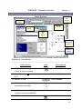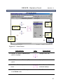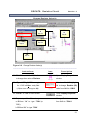
1
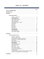
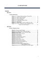
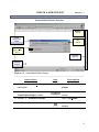
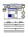
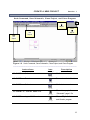
R. Moser - Desk Copy
Beginner’s User Manual for PSpice ™
Berrigan ● Beals ● Bird
TABLE OF CONTENTS
PAGE
LIST OF ILLUSTRATIONS …………….…………………………………………………
1
INTRODUCTION ……………………….…………………………………………………
2
SECTION 1 …………………………………………………………………………………
3
Create a New Project
Section 1 – Check List …………………………………………………
Create a Folder……………………………………………………………
Save to Floppy Disk ……………………………………………………
Open PSpice™ Program …………………………………………………
Open a New Project ……………………………………………………
Select a Directory…………………………………………………………
Create Blank PSpice™ Project …………………………………………
Add Libraries………………………………………………………………
Place Part …………………………………………………………………
Move Part ………………………………………………………………..
Enlarge Part ……………………………………………………………..
Shrink Part ……………………………………………………………….
Remove a Part …………………………………………………………..
Undo Command …………………………………………………………
Save Schematic …………………………………………………………
Close PSpice Project ……………………………………………………
Close Orcad Program …………………………………………………
3
4
4
5
6
7
8
9
10
11
11
11
11
12
12
12
12
SECTION 2 …………………………………………………………………………………
13
Circuits: Resistive Circuit
Section 2 – Check List …………………………………………………
Re-open Orcad Program ……………………………………………….
Re-open PSpice™ Folder and Project File …………………………..
Open PSpice™ Project Schematic Page 1 …………………………..
Place Ground …………………………………………………………….
Assign Value to Ground …………………………………………………
Place Resistor ……………………………………………………………
Rotate Resistor …………………………………………………………
Change Resistor Values…………………………………………………
Place Power Supply ……………………………………………………
Wire Circuit ………………………………………………………………
Place Junction (Node) …………………………………………………
Wire Junction to Ground ………………………………………………
Create a New Simulation File……………………………………………
Voltage Analysis ……….. ………………………………………………
Current Analysis in Amperes and Power Analysis in Watts …………
Save File, Print Schematic, and Close Program………………………
13
14
15
16
17
18
19
20
21
22
23
24
25
26
27
28
29
GLOSSARY ...........................……….……………………………………………………
30
ii
ILLUSTRATIONS
FIGURES
SECTION 1
Create a New Project
Figure
Figure
Figure
Figure
Figure
Figure
Figure
Figure
Figure
1-1
1-2
1-3
1-4
1-5
1-6
1-7
1-8
1-9
Create a Folder and Save to Floppy Disk ……………
Open PSpice™ Program ………………………………
Open a New Project …………………………………
Select a Directory ………………………………………
Create Blank PSpice Project …………………………
Add Libraries ...…………………………………………
Place Part ………………………………………………
Move, Enlarge, Shrink, and Remove a Part …………
Undo Command, Save Schematic, Close
Project, and Close Program ……………………...
4
5
6
7
8
9
10
11
12
SECTION 2
Circuits: Resistive Circuit
Figure 2-1 Re-open Orcad Program ………………….………………
Figure 2-2 Re-Open PSpice™ Folder and Project ….………………
Figure 2-3 Open PSpice™ Project Schematic Page 1 ……………
Figure 2-4 Place Ground ………………………………….……………
Figure 2-5 Assign Value to Ground …………………………………
Figure 2-6 Place Resistor ………………………………………………
Figure 2-7 Rotate Resistor ……..………………………………………
Figure 2-8 Change Resistor Value(s) ..........…………………………
Figure 2-9 Place Power Supply ………………………………………
Figure 2-10 Wire Circuit ………………………………………………
Figure 2-11 Place Junction (Node) ……………………………………
Figure 2-12 Wire Junction to Ground …………………………………
Figure 2-13 Create a New Simulation File ……………………………
Figure 2-14 Voltage Analysis……………………………………………
Figure 2-15 Current Analysis in Amperes and
Power Analysis in Watts …………………
Figure 2-16 Save File, Print Schematic, and Close Program ………
14
15
16
17
18
19
20
21
22
23
24
25
26
27
28
29
1
INTRODUCTION
For many years the Electronics Department of Penn College has relied on the PSpice™
computer program to simulate and analyze electronic circuits. “SPICE” is an acronym
for Simulation Program with Integrated Circuit Emphasis. While the PSpice™ program
is an excellent tool for evaluating circuits, it can be difficult for a beginner to learn
because of the program’s atypical format. Frustration can abound for a beginner who
uses the program without an understanding of its basic structure.
As a result, three Penn College Advanced Technical Communication students chose to
write this manual to alleviate student and faculty frustration when electronic students use
the PSpice™ program for the first time. The Beginner’s User Manual for PSpice™
explains the basic structure of the program and uses a step-by-step format to help
students succeed when they simulate and analyze the PSpice™ circuits required by the
Electronics program. When students use this manual successfully, many hours of
instructional time can be saved for the electronics faculty.
The Beginner’s User Manual for PSpice™ demonstrates how to open the Orcad®
program, create a PSpice folder, open new projects, add libraries, build resistive circuits,
and analyze the results of the circuits. The manual clarifies the libraries needed to
select components so that the analysis functions will run properly; and explains how to
correctly save projects, close projects, close the PSpice folder, and close the program.
A note to the user:
Once you understand the basic structure of the program, you can apply that knowledge
to other, more complicated procedures and circuits. This manual, however, is not an
answer key. While the manual helps you learn the basics of the PSpice™ program, it
does not contain every answer to every possible dilemma that the program may present.
As an electronics student, you can continue to explore and gain more program
knowledge on your own.
The manual is designed to help you develop a confidence in circuit simulation programs,
realize the value of SPICE programs as a circuit evaluation tool, and learn the PSpice™
program as easily as possible. With the Beginner’s User Manual for PSpice™ as a
guide, you can quickly master the skills necessary to complete your first required
assignments and have a positive experience when you simulate your first circuits.
2
CREATE A NEW PROJECT
Se ct io n 1
CHECK LIST
Before Creating a New Project, check the following:
!
IBM compatible compute is used
!
Windows 98 operating system or higher is installed on computer
!
Orcad Family Release 9.2 Lite Edition is installed on computer
!
3 ½ Floppy Disk is inserted into the (A:\) drive (for saving PSpice folder and
circuit schematic files)
MOUSE CONVENTIONS (consistent with PSpice™printed literature)
The following mouse conventions are used throughout the manual:
•
•
•
•
•
•
CLICKL (click left once) to select an item.
DCLICKL (double click left) to end a mode or edit a selection.
CLICKR (click right once) to abort a mode.
DCLICKR (double click right) to repeat an action.
CLICKLH (click left, hold down, and move mouse) to drag a selected item.
Release left button when placed.
DRAG (no clicks, move mouse) to move an item.
BOLD TEXT
A Glossary (at the end of this manual) contains bold text terms with definitions
according to their use in this manual.
3
CREATE A NEW PROJECT
Se ct io n 1
Create a Folder and Save to Floppy Disk
“PSpice” folder
Step 6
Send To ►…
3 ½ Floppy
Step 7
Folder
Step 3
Windows
Desktop
Step 1
New
Step 2
Figure 1-1 Create a Folder and Save to Floppy Disk
________________________________________________________________________
Instructions
Icon
Description
(Position on Figure)
1. CLICKR (click right mouse button)
Open pull-down menu
on Windows Desktop . . .
2. CLICKL (click left mouse button)
Open New pull-down menu
on New option . . .
3. CLICKL on Folder option.
Open New Folder
4. Type “PSpice” while New Folder
Name New Folder
is highlighted . . .
5. Use Enter ← (“key” on keyboard).
End name New Folder
6. CLICKR on “PSpice” Folder . . .
Open pull-down menu
7. CLICKL on Send To ► 3 ½ Floppy.
Send Folder to (A:) drive
4
CREATE A NEW PROJECT
Se ct io n 1
Open PSpice ™ Program
Capture Lite
Edition
Step 11
Programs
Step 9
Orcad Family
Release 9.2
Lite Edition
Step 10
Start
Step 8
Windows
Desktop
Figure 1-2 Open PSpice™ Program
________________________________________________________________________
Instructions
Icon
Description
(Position on Figure)
8. CLICKL on Start icon on
“Windows Desktop” . . .
Open Windows options
(lower left)
9. CLICKL on Programs option . . .
Open Programs menu
10. CLICKL on Orcad (Orcad Family
Open Orcad program
Release 9.2 Lite Edition) option . . .
11. CLICKL on Capture Lite Edition
option.
menu
Open Capture – [Session
Log] window
5
CREATE A NEW PROJECT
Se ct io n 1
Open a New Project
Name field
Select
Directory
window
New Document
Step 12
Type “a project name”
Step 13
Analog or Mixed A/D
Step 14
Location field
New Project
window
Browse…
Step 15
Figure 1-3 Open a New Project
________________________________________________________________________
Instructions
Icon
Description
(Position on Figure)
12. CLICKL on New Document icon.
Open New Project
(upper left)
13. Type a “project name” in the
Name Project,
Name: field window.
i.e. Circuit 1, Circuit 2, etc.
14. CLICKL on Analog or Mixed A/D
radial option.
window
Select Analog or mixed
(center left)
15. CLICKL on Browse… option.
Analog/Digital project
Open Select Directory
(lower middle)
window
6
CREATE A NEW PROJECT
S e ct io n 1
Select a Directory
OK
Step 20
Select Directory
window
OK
Step 19
Directories:
a:\ options
“PsSpice”
folder
Step 18
Drives:
Menu “▼”arrow
Step 16
Drives: field
Location field
a:
Step 17
Figure 1-4 Select a Directory
________________________________________________________________________
Instructions
Icon
Description
(Position on Figure)
16. CLICKL on Drives: “▼” arrow . . .
Open Drives: pull-down
(lower right)
menu
17. CLICKL on “a:” Drives: option . . .
Select (a:) Drive
18. DCLICKL on “PSpice” folder
Highlight and select
option in “a:\” field . . .
“PSpice” folder
19. CLICKL on OK option in
Select Directory window.
Close Select Directory
(center right)
20. CLICKL on OK option in
New Project window.
window
Close New Project window
(upper middle)
7
CREATE A NEW PROJECT
S e ct io n 1
Create Blank PSpice Project
Maximize
Step 24
Create
PSpice Project
window
OK
Step 22
“Create a blank
project” radial
Step 21
Tool Pallet
(Step 23)
Schematic
Desktop
Figure 1-5 Create Blank PSpice Project
________________________________________________________________________
Instructions
Icon
Description
(Position on Figure)
21. CLICKL on Create a blank project
Select Create a blank
radial option . . .
project
22. CLICKL on OK option in
Create PSpice Project window.
Close Create a Project
(center right)
window
23. CLICKL on “Schematic Desktop”.
Open Tool Palette
24. CLICKL on “Maximize” icon.
Maximize schematic
(upper right)
desktop
8
CREATE A NEW PROJECT
S e ct io n 1
Add Libraries
Place Part
window
Place Part
Step 25
Add Library…
Step 26
Libraries
Step 27
Open
Step 28
Figure 1-6 Add Libraries
________________________________________________________________________
Instructions
Icon
Description
(Position on Figure)
25. CLICKL on Place Part icon . . .
Open Place Part window
(upper right)
26. CLICKL on Add Library… option.
Open Browse File window
(center right)
27. While holding down Shift key
Select all Libraries
on keyboard, CLICKL (highlight) all
Library options . . .
28. CLICKL on Open option.
Open highlighted Libraries
(lower middle)
and close Browse File
9
CREATE A NEW PROJECT
Place Part
window
S e ct io n 1
Arrow
Icon
Step 32
Place Part
OK
Step 30
Part: field
Type “C”
Step 29
Place
C1
Step 31
Schematic
Desktop
Figure 1-7 Place Part
________________________________________________________________________
Instructions
Icon
Description
(Position on Figure)
29. From Place Part window, type “C”
Locate Capacitor
or “c” in Part: entry field . . .
30. CLICKL on OK option.
Select Capacitor
(upper middle)
31. CLICKL on “Schematic Desktop”
Place Capacitor on
to place capacitor (C1) . . .
schematic desktop
(center right)
32. CLICKL on “Arrow” icon . . .
End place Capacitor
(upper right)
33. CLICKL on “Schematic Desktop”.
mode
End Place Part mode
10
CREATE A NEW PROJECT
S e ct io n 1
Move, Enlarge, Shrink, and Remove a Part
Zoom Out
Step 36
Zoom In
Step 35
C1
Step 34
Highlight
C1
Step 37
Figure 1-8 Move, Enlarge, Shrink, and Remove a Part
________________________________________________________________________
Instructions
Icon
Description
(Position on Figure)
34. CLICKLH (click and hold on mouse)
Highlight entire Capacitor
on center of capacitor C1 to “drag”
(C1) and move to another
to another location . . .
(center right to left)
35. CLICKL on Zoom in icon.
Enlarge Capacitor size on
(upper center)
36. CLICKL on Zoom out icon.
37. To remove capacitor, CLICKL on
schematic desktop
Highlight Capacitor (C1)
center of capacitor “C1” to highlight
38. Press Delete key on keyboard.
schematic desktop
Shrink Capacitor size on
(upper center)
entire part . . .
location
part
(lower left)
Remove Capacitor from
schematic desktop
11
CREATE A NEW PROJECT
S e ct io n 1
Undo Command, Save Schematic, Close Project, and Close Program
“Upper”
X
Step 43
Save
Icon
Step 40
Undo
Icon
Step 39
“Lower”
X
Step 42
Figure 1-9 Undo Command, Save Schematic, Close Project, and Close Program
________________________________________________________________________
Instructions
Icon
Description
(Position on Figure)
39. CLICKL on Undo icon.
Undo last command
(upper left)
40. CLICKL on Save icon.
Save schematic to A:\ drive
(upper left)
41. CLICKL on Undo icon.
Undo last command
(upper left)
42. CLICKL on “lower X” Close icon.
Close “new project” (upper right)
43. CLICKL on “upper X” Close icon.
“Schematic” page1 file
Close “PSpice” folder
(upper right)
and Orcad® program
12
CIRCUITS: Resi st i ve Ci r cui t
Sect ion 2
CHECK LIST
Before simulating a Resistive Circuit, check the following:
!
Section 1 of this manual “Creating a New Project" is complete
!
3 ½ Floppy disk with saved PSpice folder is inserted into the correct drive
MOUSE CONVENTIONS (consistent with PSpice™printed literature)
The following mouse conventions are used throughout the manual:
•
•
•
•
•
•
CLICKL (click left once) to select an item.
DCLICKL (double click left) to end a mode or edit a selection.
CLICKR (click right once) to abort a mode.
DCLICKR (double click right) to repeat an action.
CLICKLH (click left, hold down, and move mouse) to drag a selected item.
Release left button when placed.
DRAG (no clicks, move mouse) to move an item.
BOLD TEXT
A Glossary (at the end of this manual) contains bold text terms with definitions
according to their use in this manual.
13
CIRCUITS: Resi st i ve Ci r cui t
Se ct ion 2
Re-open Orcad Program
Capture CIS
Lite Edition
Step 4
Programs
Step 2
Orcad
Step 3
Start
Step 1
Windows
Desktop
Figure 2-1 Re-open Orcad Program
________________________________________________________________________
Instructions
Icon
Description
(Position on Figure)
1. CLICKL on Start icon on
“Windows Desktop” . . .
Open Windows options
(lower left)
2. CLICKL on Programs option . . .
Open Programs menu
3. CLICKL on Orcad ( Orcad Family
Open Orcad program
Release Lite Edition) option . . .
4. CLICKL on Capture CIS Lite
Edition option . . .
menu
Open Capture – [Session
Log] window
14
CIRCUITS: Resi st i ve Ci r cui t
Se ct ion 2
Re-Open PSpice ™ Folder and Project
“▼” arrow
Step 6
Open Document
icon
Step 5
OK
Step 4
PSpice
folder
Step 8
3 1/2 Floppy (A:)
Step 7
Open
Step 10
Figure 2-2 Re-Open PSpice™ Folder and Project
________________________________________________________________________
Instructions
Icon
Description
(Position on Figure)
5. CLICKL on Open Document
icon . . .
Open Open window
(upper left)
6. CLICKL on “▼” arrow in the
Look in: filed . . .
Open My Documents pull(upper middle)
7. CLICKL on 3 ½ Floopy (A:)* . . .
*Note: (computer drive letter may vary)
down menu options
Open 3 ½ Floppy (A:) pull
(center)
8. CLICKL on PSpice folder . . .
down folder options
Select PSpice folder
(center left)
9. CLICKL on “Project Name” file . .
Select “Project Name” file
.
10. CLICKL on Open option.
Open Project file
(lower right)
15
CIRCUITS: Resi st i ve Ci r cui t
Se ct ion 2
Open PSpice ™ Project Schematic Page 1
Design Resources - Step 11
.\project name.dsn - Step 12
SCHEMATIC1 - Step 13
PAGE1 - Step 14
Figure 2-3 Open PSpice™ Project Schematic Page 1
________________________________________________________________________
Instructions
Icon
Description
(Position on Figure)
11. CLICKL on Design Resources.
Open Design Resources
(upper left)
12. DCLICKL on “.\project name.dsn
project file . . .
13. DCLICKL
on
folder
Select .\project name.dsn
(upper left)
SCHEMATIC1
project file
Open SCHEMATIC1
folder . . .
folder
(upper left)
14. DCLICKL on PAGE1.
Select PAGE1 schematic
(upper left)
16
CIRCUITS: Resi st i ve Ci r cui t
Se ct ion 2
Place Ground
Schematic
Desktop
Step 15 & 19
Tool Pallet
(Step 15)
OK
Step 18
GND/CAPSYM
Step 17
Place
Ground
Step 16
Ground
Step 19
Schematic
Desktop
Figure 2-4 Place Ground
________________________________________________________________________
Instructions
Icon
Description
(Position on Figure)
15. CLICKL (click left mouse) any where
Open Tool Palette
on Schematic Desktop.
16. CLICKL Place Ground icon
to begin to simulate resistive circuit.
Open Place Ground
(center right)
17. CLICKL GND/CAPSYM in window.
window
Select specific Ground
18. CLICKL OK to select ground.
(upper middle)
19. CLICKL on “Schematic Desktop” . .
Place Ground
(lower left)
20. CLICKR on Ground to highlight . .
Open pull-down menu
21. CLICKL on End Mode.
End Place Ground mode
17
CIRCUITS: Resi st i ve Ci r cui t
Se ct ion 2
Assign Value to Ground
Name
field
Property
Editor
Apply
Step 26
X
Close
Step 27
Ground
Step 22
Type “0”
Steps: 23,
24, 25
Figure 2-5 Assign Value to Ground
________________________________________________________________________
Instructions
Icon
Description
(Position on Figure)
22. DCLICKL on Ground symbol
Highlight Ground and open
on schematic desktop . . .
Property Editor window
(lower left)
23. * Place cursor after “D” in “GND”
*Caution:
Program will close if “GND”
in Name: field
of Property Editor window.
(upper middle)
is highlighted to delete.
24. Backspace to remove “GND” . . .
25. Type “0” in Name field of Property
Set Ground value at “0”
Editor . . .
26. CLICKL on Apply . . .
Assign Ground value “0”
(upper left)
27. CLICKL on Close icon in Property
Editor window.
Close Property Editor
(upper right)
window
18
CIRCUITS: Resi st i ve Ci r cui t
Se ct ion 2
Place Resistor
Arrow
Icon
Step 33
Type “R”
Step 29
Place Part
Step 28
OK
Step 30
Place
R1
Step 31
Place
R2 and R3
Step 32
Schematic
Desktop
Figure 2-6 Place Resistor
________________________________________________________________________
Instructions
Icon
Description
(Position on Figure)
28. CLICKL Place Part icon
to begin to place first resistor . . .
Open Place Part window
(upper right)
29. Type “R” (or “r”) in Part: entry
Locate a Resistor
field . . .
30. CLICKL on OK . . .
Select Resistor
(upper middle)
31. CLICKL on “Schematic Desktop”
Place Resister
to place first resistor (R1).
(upper middle)
32. CLICKL on “Schematic Desktop”
Place more Resistors
to place more resistors (R2, R3).
33. CLICKL on “Arrow” icon.
End Place Part mode
19
CIRCUITS: Resi st i ve Ci r cui t
Se ct ion 2
Rotate Resistor
Rotate
90û
Step 36
R2
Steps 34 & 35
Pull-down
menu
Step 35
Schematic
Desktop
Step 37
Schematic
Desktop
Figure 2-7 Rotate Resistor
________________________________________________________________________
Instructions
Icon
Description
(Position on Figure)
34. CLICKL on center of Resistor (R2)
Highlight entire R2
symbol to highlight . . .
center
35. CLICKR on center of Resistor (R2)
Open pull-down menu
symbol . . .
36. CLICKL on Rotate in pull-down
menu . . .
37. CLICKL on “Schematic Desktop”
Rotate Resistor 90û on
schematic desktop
End Rotate mode
to end Rotate mode.
20
CIRCUITS: Resi st i ve Ci r cui t
Se ct ion 2
Change Resistor Value(s)
R1 and R3
1k
Step 41a
Type “1.5Meg”
Step 39
R2
1k
Step 38
Type “750 k”
Step 41b
OK
Step 40
Figure 2-8 Change Resistor Value(s)
________________________________________________________________________
Instructions
Icon
Description
(Position on Figure)
38. DCLICKL on “1k” of R2 in the
Open Display Properties
to change ohm value of Resistor.
window
(center right)
39. *Type “1.5Meg” (MEG or meg)
* Caution: DO NOT highlight
1k to change Resistor (R2)
for 1.5 M* in Value: entry field.
(*PSpice does not recognize “M”)
(upper left)
40. CLICKL on OK to close screen.
Close Display Properties
(lower left)
41. Repeat steps 34 – 36 to change:
a. R1 from “1k” to: type “750k” (or
value from 1k Ω to 1.5M Ω
window
Change Resistors value(s)
from 1k Ω to 750k Ω
750K).
b. R3 from“1k” to: type “750k”.
21
CIRCUITS: Resi st i ve Ci r cui t
Se ct ion 2
Place Power Supply
Place Part
Step 42
Type “Vdc”
Step 43
Place Vdc
Step 45
Type “6”
Step 48
Schematic
Desktop
Figure 2-9 Place Power Supply
________________________________________________________________________
Instructions
Icon
Description
(Position on Figure)
42. CLICKL on Place Part icon
to place power supply in circuit.
Open Place Part window
(upper right)
43. Type “Vdc” in Part: entry field . . .
Locate Power Supply
44. CLICKL OK to select a dc voltage
Selects Vdc power supply
power supply (source voltage) . . .
45. CLICKL on “Schematic Desktop”.
Place Vdc in circuit
46. Press “ESC” key on upper left of
End Place Part mode
keyboard.
47. DCLICKL on “0Vdc” of Power
Supply . . .
Opens Display Properties
window
48. Type “6”Vdc in Value: field . . .
Change from 0 to 6 Vdc
49. CLICKL on OK option.
Select 6Vdc as source V
22
CIRCUITS: Resi st i ve Ci r cui t
Se ct ion 2
Wire Circuit
Red Dot
Step 52
Arrow icon
Step 54
Place Wire
Step 50
NOT
Wire
connection
Step 51
Figure 2-10 Wire Circuit
________________________________________________________________________
Instructions
Icon
Description
(Position on Figure)
50. *CLICKL on “Place Wire” icon
To begin to wire circuit . . .
* Caution: See
(upper right)
51. Place cursor over the “□” top end of
Figure 2-9
Open Place Wire mode
Attach first part of Wire
Vdc, then CLICKL . . .
52. Move cursor to end of next part (R1)
Attach last part of Wire
until the “● “ appears, then CLICKL.
53. Continue to Place Wire(s) between
Note: DO NOT wire Ground
parts until continuous path is formed.
yet
54. CLICKL on “Arrow” icon.
End Place Wire mode
(upper right)
23
CIRCUITS: Resi st i ve Ci r cui t
Se ct ion 2
Place Junction (Node)
Place
Junction
Step 55
Junction
Step 56
Figure 2-11 Place Junction (Node)
________________________________________________________________________
Instructions
Icon
Description
(Position on Figure)
55. CLICKL on “Place Junction” icon
Open Place Junction
to begin to connect Junction
to GND . . .
56. CLICKL on wire in circuit where
mode
(center right)
Place Junction in Wire
junction is desired . . .
57. CLICKR on Junction . . .
Opens pull-down menu
58. CLICKR on End Mode.
Ends Place Junction mode
24
CIRCUITS: Resi st i ve Ci r cui t
Se ct ion 2
Wire Junction to Ground
Place Wire
Step 59
NOT
Junction
Step 60
Wire
connection
Step 61
Figure 2-12 Wire Junction to Ground
________________________________________________________________________
Instructions
Icon
Description
(Position on Figure)
59. CLICKL on “Place Wire” icon
to begin to wire Junction to GND.
60. Place cursor “ ┼ ” over Junction
at node “●“; then CLICKL . . .
61. Move cursor “ ┼ ” over the top of
GND symbol until a “●“ appears,
Open Place Wire mode
(upper right)
Attach first part of Wire to
Junction
Attach last part of Wire to
Ground
then, CLICKL . . .
62. Press “ESC” key on keyboard.
End Place Wire mode
25
CIRCUITS: Resi st i ve Ci r cui t
PSpice
Step 63
Se ct ion 2
Create a New Simulation File
New
Simulation
Step 64
Create
Step 66
Name:
field
Type
“Voltage Analysis”
Step 65
OK
Step 67
Figure 2-13 Create a New Simulation File
________________________________________________________________________
Instructions
Icon
Description
(Position on Figure)
63. CLICKL on PSpice option in
menu bar . . .
Open New Simulation
(upper left)
64. CLICKL on New Simulation
Profile . . .
window
Open New Simulation
(upper left)
65. Type “Voltage Analysis” in
Profile file
Name New Simulation
Name: field . . .
Profile file
66. CLICKL on Create .
Close New Simulation
(center)
67. CLICKL on OK option.
window
Return to Schematic
(lower right)
Desktop
26
CIRCUITS: Resi st i ve Ci r cui t
Se ct ion 2
Voltage Analysis
PSpice
Step 69
V (Voltage)
icon
Step 68
Run icon
Step 70
Schematic
window
X icon
Step 71
Figure 2-14 Voltage Analysis
________________________________________________________________________
Instructions
Icon
Description
(Position on Figure)
Select Voltage analysis for
68. CLICKL on “V” (Voltage) icon
(may already be selected). . .
(upper middle)
69. CLICKL on PSpice option in menu
bar . . .
every node in circuit
Open pull-down PSpice
(upper left)
70. CLICKL on Run icon . . .
menu options
Open “New Simulation” file
(upper left)
71. CLICKL on X of Schematic
window to close and view voltage.
Close Schematic window
(upper left)
27
CIRCUITS: Resist i ve Ci rcui t
Se ct io n 2
Current Analysis in Amperes and Power Analysis in Watts
V (Voltage)
W (Power)
icon
Step 72
icon
Step 74
I (Current)
Schematic
Desktop
icon
Step 73
Relocate
I (Current) Value
Step 73
Figure 2-15 Current Analysis in Amperes and Power Analysis in Watts
________________________________________________________________________
Instructions
Icon
Description
(Position on Figure)
Deselect Voltage values
72. CLICKL on “V” (Voltage) icon.
(upper middle)
Select Current analysis for
67. CLICKL on “I” Current icon . . .
(upper middle)
every node in circuit
Select Power analysis for
68. CLICKL on “W” Power icon . . .
(upper middle)
69. CLICKH (click and hold on mouse) on
every node in circuit
Highlight and drag to new
center of any analysis value to
highlight and drag to new location. .
from every node in circuit
location
(lower middlet)
Deselect Current and
70. CLICKL on “I” and “W” icon
(upper middlet)
Voltage analysis
28
CIRCUITS: Resi st i ve Ci r cui t
Se ct ion 2
Save File, Print Schematic, and Close Program
“Upper”
X
Step 75
Print
Icon
Step 72
“Lower”
X
Step 73
Save
Icon
Step 71
Figure 2-16 Save File, Print Schematic, and Close Program
________________________________________________________________________
Instructions
Icon
Description
(Position on Figure)
71. CLICKL on Save icon.
Save schematic to A:\ drive
(upper left)
72. CLICKL on Print icon . . .
Print Resistive Circuit
(upper left)
73. CLICKL on “lower X” Close icon.
simulated schematic
Close “new project” -
(upper right)
74. CLICKL on Yes option.
“Schematic” page1 file
Save changes to schematic
page.
75. CLICKL on “upper X” Close icon . .
.
76. CLICKL on Yes All option.
Close “PSpice” folder
(upper right)
and Orcad® program
Save All to floppy disk
29
GLOSSARY
Note: The terms are defined according to their use in the manual.
Ω (symbol) Ohms, a unit of resistance
1k 1,000; a resistor value in Ohms (Ω)
1Meg 1,000,000; a resistor value in Ohms (Ω)
750k 750,000; a resistor value in Ohms (Ω)
Analog or Mixed A/D Option for Analog or Analog and Digital
Arrow (icon) End current mode
Browse Search through file directories
Capture Lite Edition Open PSpice [Session log]
CLICKL Click Left on mouse
CLICKLH Click Left and Hold on mouse to drag
CLICKR
Click Right
Create PSpice Project Open a new document and blank project
DC Direct Current
DC Direct Current
DCLICKL Double Click Left on mouse
Drag Moves the highlighted object on desktop
GND/CAPSYM Specific ground type
Edit Properties Pull-down menu with editing options
End Mode End the mode of selected function
I Current analysis option in Amperes
Junction A node or specific place in the wire of between components
New Open new folder on “Windows” desktop
New Project Menu options for new project
Orcad Family Release 9.2 Lite Edition Program that contains PSpice™
30
GLOSSARY
Continued…
Part : Entry field for part search
Place Ground Mode to place selected ground symbol on schematic desktop
Place Junction Mode to place junction node in wire
Place Part Mode to locate and place selected part on schematic desktop
Place Wire Mode to place wire between parts on schematic desktop
Power Supply Voltage source, i.e. Vdc, Vac
Programs ► Open “Program” menu options
Property Editor Window with component property options
R Resistor
R2 Resistor label for 2nd resistor
Rotate Mode to rotate a selected part 90°
Select Directory Open “Directory” options
Send To 3 ½ Floppy ► Pull-down menu option to move folder from
“Windows” desktop to (A:\) drive
V Voltage analysis option in volts
Vac Voltage source with Alternating Current
Vdc Voltage source with Direct Current
W Power analysis option in Watts
31