1
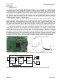
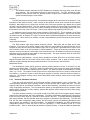
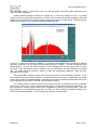
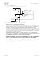
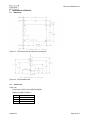
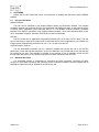
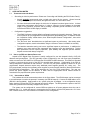
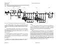
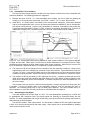
DP5 User Manual Rev A1
DP5 User Manual and Operating Instructions
Amptek, Inc.
14 DeAngelo Dr.
Bedford, MA 01730
PH: +1 781-275-2242 FAX: +1 781-275-3470
[email protected] www.amptek.com
Other DP5 related documents:
•
DP5 Quick Start Guide
•
DP5 Programmer’s Guide
•
DP5 Product Change Document
•
PC5 User Manual
•
Grounding and Shielding the DP4 Product Family
Amptek Inc.
Page 1 of 31
DP5 User Manual Rev A1
Table of Contents
1
Introduction........................................................................................................................................3
2
Understanding the DP5 .....................................................................................................................4
2.1
Major Function Blocks...................................................................................................................4
2.2
Analog Prefilter..............................................................................................................................5
2.3
Pulse Shaping ...............................................................................................................................7
2.3.2
Pulse Selection.....................................................................................................................9
2.3.3
MCA, MCS, Counters, and SCAs ......................................................................................11
2.3.4
Electrical & Software Interfaces .........................................................................................12
3
Specifications ..................................................................................................................................14
4
Electrical Interfaces .........................................................................................................................17
4.1
Electrical specifications...............................................................................................................17
4.1.1
Absolute Maximum Ratings ...............................................................................................17
4.1.2
DC Characteristic ...............................................................................................................17
4.2
Auxiliary Input and Outputs.........................................................................................................18
4.3
Timing of Auxiliary Inputs and Outputs .......................................................................................19
4.4
Analog Input ................................................................................................................................21
4.5
Interconnect ................................................................................................................................21
4.5.1
5
Power Supply Architecture .................................................................................................22
Mechanical Interface .......................................................................................................................23
5.1
Dimensions .................................................................................................................................23
5.2
Connectors..................................................................................................................................23
6
Software ..........................................................................................................................................26
6.1
Interface Software .......................................................................................................................26
6.2
Embedded Software ...................................................................................................................26
7
Application notes .............................................................................................................................27
7.1
Troubleshooting and Advice .......................................................................................................27
7.2
Use of the DP5 with Amptek Detectors ......................................................................................27
7.2.1
Users with an XR100..........................................................................................................27
7.2.2
Users with a PA-210 or PA-230 Preamplifier .....................................................................28
7.3
How to configure the analog prefilter for custom applications ....................................................29
7.3.1
Description of Analog Prefilter Circuit ................................................................................29
7.3.2
Preamplifier Tail Cancellation ............................................................................................30
7.3.3
Attenuating Preamp Signal ................................................................................................30
7.3.4
Other Custom Configurations.............................................................................................31
Amptek Inc.
Page 2 of 31
DP5 User Manual Rev A1
1
INTRODUCTION
The DP5 is a high performance digital pulse processor. It is one component in a complete nuclear
spectroscopy system, which generally also includes (1) a detector and preamplifier and (2) power supplies.
A complete system can be assembled by combining the DP5 with one of Amptek’s detectors and preamps
(several options and configurations may be used) and with Amptek’s PC5 power supply. Alternately, a user
can supply his own detector, preamplifier, and/or power supply. Although designed primarily for use with
high resolution solid state detectors, the DP5 has been used with scintillator/PMT systems, proportional
counters, and a wide variety of other detectors. The DP5 is a printed circuit board assembly, suited primarily
to OEM applications as part of a complete system.
The DP5 is a second generation digital pulse processor (DPP) which replaces both the shaping
amplifier and MCA found in analog systems. The digital technology improves several key parameters: (1)
better performance, specifically better resolution and higher count rates; (2) greater flexibility since more
configuration options are available, selected by software, and (3) improved stability and reproducibility. The
DPP digitizes the preamplifier output, applies real-time digital processing to the signal, detects the peak
amplitude, and bins this in its histogram memory. The spectrum is then transmitted to the user’s computer.
In its standard configuration, only three connections are required: power (+5 VDC), communications
(USB, RS232, or Ethernet), and an analog input from the preamplifier. An auxiliary connector provides
several additional inputs and outputs, used if the DP5 will be integrated with other equipment. This includes
an MCA gate, timing outputs, and eight SCA outputs. The DP5 also includes an “interconnect”, designed
principally to interface with Amptek’s power supply boards but available to OEMs. The DP5 is supplied with
the ADMCA data acquisition and control software, along with a DLL library of interface routines, to integrate
the unit with custom software. Optional accessories include software for analyzing X-ray spectra, several
collimation and mounting options, and X-ray tubes to complete a compact system for X-ray fluorescence.
Figure 1-1. Photograph of DP5 (left) and a typical 55Fe spectrum (right), obtained with an XR-100SDD.
USB
RS232
Ethernet
Preamp Out
PC5
XR-100SDD
X-ray Detector
and Preamplifier
Detector &
Preamp Power
Supplies
DP5
Computer
+5VDC
Control
Readout
Digital Pulse
Processor
+5VDC
AC
Power
Adapter
Detector H.V., Cooler
Power, Preamp Power
Figure 1-2. Block diagram of the X-123SDD, which uses the DP5 as part of a complete system.
Amptek Inc.
Page 3 of 31
DP5 User Manual Rev A1
2
UNDERSTANDING THE DP5
A complete, typical nuclear spectroscopy system includes a few key components: (1) the detector, (2)
the preamplifier, (3) the pulse processing electronics (which include pulse shaping, pulse selection logic,
pulse counters, a multichannel analyzer, and interfaces for data acquisition and control), (4) the power
supplies, (5) the packaging or enclosure for the system, and (6) the computer running software for instrument
control, data acquisition, and data analysis. The DP5 is a single board digital pulse processor which
implements the functions described in (3). It is one component in a complete system. It was designed for
maximum flexibility, to be tailored for use in a wide variety of systems. As a board level solution, it is most
appropriate for OEM integration into complete instruments. This section of the User’s Manual provides some
background information on the DP5 and its design and function. Later sections will provide detailed
specification and application information. 1
2.1
MAJOR FUNCTION BLOCKS
Figure 2-1 shows how a Digital Pulse Processor (DPP) is used in the complete signal processing chain
of a nuclear instrumentation system and its main function blocks. The DPP digitizes the preamplifier output,
applies real-time digital processing to the signal, detects the peak amplitude (digitally), and bins this value in
its histogramming memory, generating an energy spectrum. Pulse selection logic can reject pulses from the
spectrum, using a variety of criteria. The spectrum is then transmitted over the DPP’s interface to the user’s
computer.
Digital Pulse Shaping
Detector and
Preamplifier
Analog
Prefilter
ADC
Slow
Channel
Peak Detect
Histogram Logic
Counters
Fast
Channel
Pulse
Selection
μC and
Interface
Auxiliary
Signals
Computer
Oscilloscope or
external logic
Digital Processor (DPP)
Figure 2-1. Block diagram of a Digital Pulse Processor (DPP) in a complete system.
Analog Prefilter: The input to the DP5 is the output of a charge sensitive preamplifier. The analog prefilter
circuit prepares this signal for accurate digitization. The main functions of this circuit are (1) applying
appropriate gain and offset to utilize the dynamic range of the ADC, and (2) carrying out some filtering and
pulse shaping functions to optimize the digitization.
ADC: The 12-bit ADC digitizes the output of the analog prefilter at a 20 or 80 MHz rate. This stream of
digitized values is sent, in real time, into the digital pulse shaper.
Digital Pulse Shaper: The ADC output is processed continuously using a pipeline architecture to generate
a real time shaped pulse. This carries out pulse shaping as in any other shaping amplifier. The shaped
pulse is a purely digital entity. Its output can be routed to a DAC, for diagnostic purposes, but this is not
necessary.
There are two are two parallel signal processing paths inside the DPP, the “fast” and “slow” channels,
optimized to obtain different data about the incoming pulse train. The “slow” channel, which has a long
shaping time constant, is optimized to obtain accurate pulse heights. The peak value for each pulse in the
slow channel, a single digital quantity, is the primary output of the pulse shaper. The “fast” channel is
optimized to obtain timing information: detecting pulses which overlap in the slow channel, measuring the
incoming count rate, measuring pulse risetimes, etc. and to obtain
1
This section presumes familiarly with radiation detection. For additional information, we recommend:
G.F. Knoll, Radiation detection and measurement, 3rd edition, John Wiley & Sons, 2000.
H. Spieler, Semiconductor detector systems, Oxford University Press, 2005.
R. Jenkins, R.W. Gould, D. Gedcke, Quantitative X-ray spectrometry, 2nd edition, Marcel Dekker, Inc., 1995.
G. Gilmore, J. Hemingway, Practical gamma-ray spectrometery, John Wiley & Sons, 1995.
Amptek Inc.
Page 4 of 31
DP5 User Manual Rev A1
Pulse Selection Logic: The pulse selection logic rejects pulses for which an accurate measurement cannot
be made. It includes pile-up rejection, risetime discrimination, logic for an external gating signal, etc.
Histogram Memory: The histogram memory operates as in a traditional MCA. When a pulse occurs with a
particular peak value, a counter in a corresponding memory location is incremented. The result is a
histogram, an array containing, in each cell, the number of events with the corresponding peak value. This is
the energy spectrum and is the primary output of the DPP. The unit also includes several counters, counting
the total number of selected pulses but also counting input pulses, rejected events, etc. Auxiliary outputs
include eight different single channel analyzers, and both a DAC output and two digital outputs showing
pulse shapes selected from several points in the signal processing chain.
Interface: The DP5 includes hardware and software to interface between these various functions and the
user’s computer. A primary function of the interface is to transmit the spectrum to the user. The interface
also controls data acquisition, by starting and stopping the processing and by clearing the histogram
memory. It also controls certain aspects of the analog and digital shaping, for example setting the analog
gain or the pulse shaping time. The DPP includes USB, RS232, and Ethernet interfaces.
The DP5 also includes a power interface. It takes a loosely regulated 5VDC input and generates the various
levels required by the circuitry (+/- 5.5V, 3.3V, 2.5V).
2.2
ANALOG PREFILTER
The DP5 was designed to process signals coming directly from a charge sensitive preamplifier used
with solid-state radiation detectors. These signals typically have (1) a small amplitude, in the range of a few
mV, (2) a fast rise (tens of nsec to μsec), and (3) the small pulses “ride up” on one another as the signal
pulses accumulate. These steps can be seen in the top traces of Figure 2-2 and are not suitable to be
directly digitized, due to the small amplitude (a few mV) over the large range (many volts). The analog
prefilter prepares the signal so it can be accurately digitized.
Figure 2-2. Oscilloscope traces illustrating the signal processing. The dark blue trace on top shows the
output of the preamplifier: a series of “steps” of a few millivolts, spaced randomly in time. High frequency
white noise is clearly superimposed. The traces on the left (right) were measured with 60 (5.9) keV X-rays.
The signal to noise ratio is clearly much degraded on the right. The light blue traces show the output of the
analog prefilter, with its 3.2 μsec pole. The magenta trace shows the shaped output: it is the peak of this
which is detected and is binned in the spectrum. The green trace is a logic output indicating that a valid peak
has been detected.
The prefilter implements three functions: (1) it applies a high pass filter with a 3.2 μsec time constant, so
that the pulses no longer “ride up” on one another, (2) it applies a coarse gain so that the largest pulses are
approximately 1 V (to maximize the ADC resolution), and (3) it applies a DC offset so that the signal always
falls within the range of the unipolar ADC. The output of the prefilter can be seen as the cyan color trace in
Figure 2-2 and consists of a series of pulses with a fast rise, 3.2 μsec decay, a baseline of a few hundred
Amptek Inc.
Page 5 of 31
DP5 User Manual Rev A1
millivolts, and maximum values of around 1V. The prefilter can accommodate pulses of either polarity,
inverting the signals digitally. For opposite polarity signals, the prefilter output will have a baseline of
approximately 1.8V, with negative steps of magnitude approximately 1V.
Final Amp
Inverts
Sets offset
Anit-jitter low pass filter
Unity Gain
Buffer
-
High Pass
Filter
Coarse Gain
Two amplifiers,
four gain each
3 or 13pF
3.2 μsec
2.5kΩ
+
Preamp
Output
2.5kΩ
6.8 nF
+
460 Ω
ADC
Input
DNI
or
900 Ω
Input Offset
DAC
Figure 2-3. Block diagram of the analog prefilter in the DP5.
By default, the analog prefilter of the DP5 is configured for use with Amptek’s XR100CR family of
detectors: solid state X-ray detectors with a reset preamplifier. The DP5 can certainly be used with other
detectors, but this will most often require changing the analog prefilter settings or circuit changes. The most
common changes are discussed in section 7.3 of this document.
The key to configuring the preamplifier is that the pulses input to the ADC should have the
characteristics shown in Figure 2-2. These pulses can be viewed using the ADMCA software, by using
oscilloscope mode and showing the decimated input, or by placing an oscilloscope probe on AMP3OUT.
The pulses should have a fast rise and a 3.2 μsec decay. For a preamp with a negative going output, the
ADC input should show a baseline of a few hundred millivolts and maximum values of around 1V. For a
preamp with a positive going output, the ADC input should have a baseline of about 1.8V, with negative
going pulses of magnitude about 1V.
System Gain
The system conversion gain is expressed in units of channels/keV: it gives the MCA channel number in
which a particular energy peak will occur. It is the product of three terms: (1) the conversion gain of the
charge sensitive preamplifier (in units of mV/keV), (2) the total gain of the voltage amplifier (the product of
coarse gain and fine gain), and (3) the conversion gain of the MCA (channels per mV).
For Amptek’s XR100CR detectors, the preamp conversion gain is typically 1 mV/keV. The MCA’s
conversion gain is given by the number of channels selected (for example, 1024) divided by the voltage
corresponding to the peak channel. In Amptek’s digital processors, this is approximately 950 mV. The DP5
gain is the product of the coarse and fine gains. For example, if the fine gain is 1.00 and the coarse gain is
66.3, then the system conversion gain is (1 mV/keV)(66.3)(1.00)(1025 ch/950 mV)=71.5 channels/keV. The
inverse of this is the MCA calibration factor, 14 eV/channel. The full scale energy is 1024 channels/71.5
channels per keV, or 14.3 keV. Note that these values are approximate. Due to manufacturing tolerances in
the feedback capacitors, in resistors, etc the actual gain can vary by several percent, which will cause a
noticeable shift in the spectrum. These calculations should be used for system design and for initial
configuration. For any given system, the gain will need tuning and the spectrum will need to be calibrated.
For systems other than Amptek’s XR100 series, the preamp conversion gain can be estimated. It is the
product of three terms: (1) one over the energy required to create an electron hole pair in the detector (W),
(2) any internal detector gain, e.g. with a proportional counter or PMT, and (3) the preamp’s conversion gain,
q/CF, where CF is the feedback capacitance. For example, for a Xe proportional counter, W is 21.5 eV. At a
gain of 103 and CF=1 pF, the conversion gain is (1/21.5 eV/pair)(103)(1.6x10-19 C/10-12 F)=7.4 mV/keV.
Reset and Continuous Preamplifiers
Most spectroscopy detectors utilize a charge sensitive preamplifier, which precedes the analog prefilter
in the DP5. A charge sensitive preamplifier produces a voltage proportional to the time integral of the
current. The integrator will eventually saturate because the time integral of the current through the diode
Amptek Inc.
Page 6 of 31
DP5 User Manual Rev A1
continues to increase. There are two methods used to keep the preamplifier output within range: resets and
continuous feedback. Figure 2-4 (left) shows the output of a reset preamp over a very long time: many
small steps of a few mV each causes the output to linearly approach the negative limit (-5V) in a time of
several seconds. The reset pulse occurs so the output goes to the initial value (+5V) in a few μsec. Reset
preamplifiers provide the minimum electronic noise and so are used in Amptek’s lowest noise systems,
including the XR100. The very large transient created during reset can affect signal processing, so the DPP
includes logic to “lock out” the effects of this reset.
Figure 2-4. Oscilloscope traces showing typical preamplifier outputs, for reset preamps (a) and (b) and for
continuous feedback preamps (c).
Another traditional solution is to add a slow feedback path which restores the input to a value near
ground In the simplest case, a feedback resistor RF is placed in parallel with the feedback capacitor CF on
which the current is integrated. After the voltage step ΔV due to each signal interaction, the output slowly
drifts back to its quiescent value, with the time constant of the feedback, as illustrated in Figure 2-4 (b). This
time constant is 500 μsec in this plot. The long time permits accurate integration of the total charge but
causes the pulses to pile-up on one another. The feedback resistor adds electronic noise so is not used in
the lowest noise systems. Some Amptek detectors replace the feedback resistor with a transistor. This
offers lower noise than resistive feedback but does not match the performance of the reset preamps.
The analog prefilter of the DP5 has a standard configuration which is suitable for Amptek’s XR100
family of detectors, using reset preamplifiers with fairly high gain. By appropriate configuring the prefilter, the
DPP can be used with many other detectors and preamps. Section 7.3 describes commonly used
configurations. For example, it is straightforward to change the prefilter to accommodate preamps with
continuous feedback, e.g. traditional resistive feedback. One can easily change the gain stages to
accommodate systems with particularly high or low gains. A charge amplifier can be implemented in the
prefilter and other options are available. See Section 7.3 for configuration changes which can be
implemented by a customer or contact Amptek, Inc. for more significant changes.
2.3
PULSE SHAPING
Slow Channel
The “slow channel” of the DPP is optimized for accurate pulse height measurements. It utilizes
trapezoidal pulse shaping, with a typical output pulse shape shown in Figure 2-5. This shape provides a
near optimum signal to noise ratio for many detectors. Relative to conventional analog shapers, the
trapezoid provides lower electronic noise and, simultaneously, reduced pulse pile-up.
Figure 2-5. Pulse shape produced by the DP4.
Amptek Inc.
Page 7 of 31
DP5 User Manual Rev A1
The user can adjust the rise/fall time (the rise and fall must be equal) and the duration of the flat top
over many steps. A semi-Gaussian amplifier with shaping time τ has a peaking time of 2.2τ and is
comparable in performance with the trapezoidal shape of the same peaking time. A DPP with 2.4 μsec
peaking time will be roughly equivalent to a semi-Gaussian shaper with a 1 μsec time constant.
Adjusting the peaking time is a very important element in optimizing the system configuration. There is
usually a trade-off: the shortest peaking times minimize dead time, yielding high throughput and
accommodating high count rates, but the electronic noise usually increases at short peaking times. The
optimum setting will depend strongly on the detector and preamplifier but also on the measurement goals.
The electronic noise of a detector will generally have a minimum at some peaking time, the “noise corner.”
At peaking times shorter or longer than this, there is more noise and hence degraded resolution. If this
peaking time is long relative to the rate of incoming counts, then pulse pile-up will occur. In general, a
detector should be operated at a peaking time at the noise corner, or below the noise corner as necessary to
accommodate higher count rates.
If the risetime from the preamp is long compared with this peaking time, then the output pulses will be
distorted by ballistic deficit. In this case, the trapezoidal flat top can be extended to improve the spectrum.
The specific optimum timing characteristics will vary from one type of detector to the next and on the details
of a particular application, e.g. the incoming count rate. The user is encouraged to test the variation of
performance on these characteristics.
Fast Channel
The DPP’s “fast channel” is optimized to detect pulses which overlap in the “slow channel”. The fast
channel is used for pile-up reject logic (rejecting pulses which are so closely spaced that they cannot be
distinguished in the slow channel) and for determining the true incoming count rate (correcting for events lost
in the dead time of the slow channel). The fast channel also utilizes trapezoidal shaping, but the peaking
time is commendable to either 100 nsec or 400 nsec. The oscilloscope traces in Figure 2-6 show the
measured pulse shapes with a 100 nsec peaking time. As seen on the right, pulses which are separated by
only 120 nsec are separately counted in the fast channel.
Figure 2-6. Oscilloscope traces showing operation of the DPP “fast channel”. The magenta trace at top
shows the ADC input, the light blue trace shows the fast channel shaped output, and the dark blue trace
shows the logic output which counts the fast channel events.
Baseline Restoration
The pulse height is implicitly measured relative to a baseline. Any random fluctuation or systematic
variation in the baseline, whether high frequency noise or a slow change, will degrade the pulse height
measurement. The baseline is often assumed to be “ground”, but this is a somewhat ambiguous notion,
since “ground” represents simply the reference for voltage measurements. If this baseline changes with
time, count rate, or anything else, then distortions are introduced into measurements. In pulse height
analysis, the spectrum will appear to shift, while in counting systems, the threshold will change. In practice,
the most common baseline shift occurs with count rate.
Amptek Inc.
Page 8 of 31
DP5 User Manual Rev A1
The peak of the “baseline” of a digital processor has some significant differences from traditional analog
shaping amplifiers. Because the DPP’s transfer function has a finite impulse response, after a pulse has
passed through the processing pipeline it has no impact on the output. This is fundamentally different from
an analog differentiator and results in vastly enhanced baseline stability at high count rates. However, unlike
analog shapers the DPP has to establish a DC baseline, at all count rates, and in practice some shifts with
count rate are observed.
The DPP has an asymmetric baseline restorer with several different settings. The DPP BLR uses the
negative peaks from random noise to determine the baseline. The negative-going noise peaks only occur in
the absence of a signal, so if these are stable, then the baseline is stable, independent of counts. The BLR
generally produces an offset comparable to the rms noise value. There are two independent parameters, UP
and DOWN, each of which can be set to four values: Very Slow, Slow, Medium, and Fast. These are
essentially slew rates in the baseline response. A setting of Very Fast for both UP and DOWN means that
the BLR will respond very rapidly to any measured variation in the baseline. It must be stressed that the
optimum setting depends strongly on the details of a particular application: the nature of the baseline drifts,
etc. If the peaks are found to shift to lower channels at high count rates, then increase the UP slew rate or
decrease the DOWN slew rate. If one observes occasional “bursts” in the system which cause the spectrum
to shift to higher channels (often manifesting as bursts of noise above the threshold), then decrease the UP
slow rate or increase the DOWN slew rate.
2.3.2
Pulse Selection
Thresholds
The DPP uses thresholds to identify pulses. Both fast and slow channels have their own independent
thresholds. Noise is usually higher in the fast channel, and it is best to set the thresholds just above the
noise, so they will be different in the two channels. The DPP uses the Slow Channel Threshold to identify
events that should be added to the stored spectrum. Events with an amplitude lower than the Slow Channel
Threshold are ignored – they do not contribute to the stored spectrum. The slow channel threshold is the
equivalent of a low-level discriminator (LLD).
The Fast Channel Threshold also functions as an LLD and is used for several functions. (1) The rate of
events over the fast threshold is the DPP’s measurement of the incoming count rate (ICR). (2) Pile-Up
Rejection (PUR) logic identifies events which overlap in the slow channel but are separated in the fast
channel. (3) Rise Time Discrimination (RTD) uses the amplitude of the fast channel signal to measure the
current at the beginning of a pulse. PUR and RTD are discussed in more detail below.
Properly setting these thresholds is very important for getting the best performance from the DPP.
Under most circumstances, the thresholds should be set just above the noise, and the ADMCA software
includes an “AutoTune” function to set these. Improperly set thresholds are responsible for a large number
of problems reported by customers. If the fast channel threshold is too low, for example, and PUR is
enabled, then every event will be rejected and so there appears to be no signal. If the slow channel
threshold is too high, then it is also possible to reject all events.
Pile-Up Rejection
The goal of the pile-up reject (PUR) logic is to determine if two interactions occurred so close together in
time that they appear as a single output pulse with a distorted amplitude. The DPP PUR uses a “fast-slow”
system, in which the pulses are processed by a fast shaping channel in parallel with the slower main channel
(both channels are purely digital). Though similar in principle to the techniques of an analog shaper, the pileup reject circuitry and the dead time of the DPP differ in significant ways, resulting in much better
performance at high count rates. First, the symmetry of the shaped pulse permits the dead time and pile-up
interval to be much shorter. Second, there is no dead time associated with peak acquisition and digitization,
only that due to the pulse shaping.
Figure 2-7 illustrates the operation of the DP4 for pulses that occur close in time. Figure 2-7 (a) shows
two events that are separated by less than the rise time of the shaped signal, while Figure 2-7 (b) shows two
pulses that are separated by slightly longer than the rise time. In (a), the output is the sum of the two signals
(note that the signal amplitude is larger than the individual events in (b)) and the events are said to be piled
up. However, note that the analog prefilter outputs in (a) are separate. For a nearly triangular shape, pile-up
only occurs if the two events are separated by less than the peaking time, in which case a single peak is
Amptek Inc.
Page 9 of 31
DP5 User Manual Rev A1
observed for the two events. The interval used by the DPP for both dead time and pile-up rejection is the
sum of risetime and the flat-top duration. If two events occur within this interval and pile-up rejection is
disabled, then the single, piled-up value is in the spectrum. If pile-up rejection is enabled and two events are
separated by more than the fast channel pulse pair resolution (120 nsec) and less than this interval, both are
rejected. Events that exceed a threshold in the fast channel trigger the pile-up reject logic.
(a)
(b)
Figure 2-7. Oscilloscope traces illustrating the dead time and pile-up reject performance of the DP4
Reset Lockout
As discussed previously, many preamps use pulsed reset to prevent saturation of the preamp output.
The reset generates a very large signal in the DPP, causing its amplifiers to saturate, registers to overflow,
etc. The DPP therefore includes a reset detect circuit (which detects a very large, negative going pulse) and
logic to lock out signal processing for some time following the reset, to give time for everything to return to
stable values. The DPP permits the user to enable or disable reset (it should be disabled for preamps with
continuous feedback). The user can also select the time interval during which the signal is locked out. If the
interval chosen is too short, then there will be some distortion of the waveform (and thus spectrum) following
reset. At high count rates the reset pulses occur frequently, and if the interval chosen is too long, then a
significant dead time is observed.
Risetime Discrimination
In some types of applications, it is important to separate pulses based on the duration of the transient
current through the detector, into the preamplifier. For example, in some Si diodes there is an undepleted
region with a weak electric field. A radiation interaction in this region will generate a signal current, but the
charge motion is slow through the undepleted region. These interactions in this region can lead to various
spectral distortions: background counts, shadow peaks, asymmetric peaks, etc. In CdTe diodes, the lifetime
of the carriers is so short that slow pulses exhibit a charge deficit, due to trapping. These lower amplitude
pulses distort the spectrum. In scintillators, pulse shape discrimination is sometime used to differentiate
gamma-rays and neutrons. This pulse shape discrimination can be implemented using the DP5’s RTD
function. Most Amptek detectors do not require or benefit from RTD but for some it is quite useful.
Risetime discrimination rejects from the spectrum events with a long detector current, which leads to a
slowly rising edge in the fast and slow shaped pulses. The DP5 implements RTD by comparing the peak
height in the fast channel (which samples the charge integrated in the first 100 nsec) to the peak height in
the slow channel (which samples the charge which is eventually integrated). If this ratio is sufficiently high,
the risetime was fast and thus the pulse is accepted. If this ratio is low, the pulse is rejected. Because the
fast channel is inherently much noisier than the slower shaped channel, an RTD threshold is also
implemented on the shaped channel. Events which fall below this threshold (the “RTD Slow Threshold”) are
not processed by the RTD and are thus accepted (unless otherwise rejected by Pileup Rejection or some
other criterion). Because RTD is most often needed on interactions deep in a detector, arising from highenergy events, low-amplitude events are unlikely to benefit from RTD rejection. These fall below the RTD
Slow Threshold and are thus accepted.
Gate
The gate input is used with external circuitry to determine if events should be included or excluded from
the spectrum. The gate can be active high or active low (or disabled). If disabled, then this input is ignored
Amptek Inc.
Page 10 of 31
DP5 User Manual Rev A1
and all events (which meet the criteria above) are counted. If active high (low), then if the gate input is high
(low), the event is counted in the spectrum. When counts are gated off, the clock accumulation time counter
is also gated off so that an accurate count rate can be determined. The timing of this gate input is important.
If the gate input is active while the fast channel threshold is triggered, then the event is counted as a fast
count. If the gate input is active when the peak detect is triggered, then the event is counted as a slow count
and shows up in the spectrum. Note that the fast and slow channels are triggered at different times, since
they have different shaping times.
2.3.3
MCA, MCS, Counters, and SCAs
Multichannel Analyzer
The MultiChannel Analyzer (MCA) operates like a conventional MCA, except that the input is already
digitized. It detects the amplitude of the peak of the shaped pulse, using a digital peak detect circuit. If the
selection logic indicates that the pulse is valid, then it increments the value stored at a memory location
corresponding to the peak amplitude. The MCA supports 256, 512, 1024, 2048, 4096 or 8192 channels. The
DP5 uses 3 bytes per channel, which allows up to 16.7M counts per channel.
The MCA hardware in the DP5 can be started and stopped by commands over the serial bus. It can
also be preset to stop after a programmed acquisition time (with a minimum of 100 milliseconds) or after a
programmed number of counts has been measured within the SCA8 region of interest (see below).
Acquisition Time
The DPP measures the spectrum and counts during the “acquisition time”, which is also measured and
reported. The acquisition time is the real elapsed time during which data are being acquired. The
acquisition time clock is turned off during certain events, including data transfers over the serial bus and
including reset intervals. If a reset preamplifier is used, and the DP5 is configured for a certain reset time
period, then acquisition is shut down during the reset period and the acquisition clock is stopped. This
acquisition time is measured using a typical 50 ppm crystal oscillator so is quite accurate. The true count rate
should be computed using the actual acquisition time rather than the nominal data transfer time.
Data transfers occur based on an approximate real time clock in the host PC. For example, one might
configure ADMCA to acquire data from the DP5 every second. When the data transfer occurs, the
acquisition time is shown and this will probably differ from the nominal “1 second”, due to the approximate
clock and also due to reset losses. (A typical value is 1.05 second.) At high count rates, a reset preamp
resets more often, and so there is less acquisition time per transfer. In this case, the acquisition time might
become 0.85 seconds. On the screen, this time is displayed along with the fast counts and the slow counts
during the same interval. The actual count rate is found by dividing the observed counts by the observed
acquisition time, 0.85 seconds for this example.
Dead Time
All nuclear spectroscopy systems exhibit a dead time associated with each radiation interaction.
Following any interaction, there will be a time period during which subsequent pulses cannot be detected and
will not contribute to the output counts. Because the timing of pulses is random, there is always some
probability that pulses will occur in these dead time intervals, and therefore the output count rate (Rout)
measured by a system is always lower than the input count rate (Rin). The measurement goal is to
determine the incident spectrum and count rate, which requires correcting for these losses.
The dead time characteristics of a digital processor differ considerably from those of more traditional
analog systems. This is discussed in some detail in an Amptek application note and a research publication.
Some key points are:
•
The deadtime per pulse of a digital processor is lower than that of a comparable analog system.
There is no deadtime associated with acquiring the peak (this is termed simply the deadtime in an
analog MCA and often dominates system deadtime) and the deadtime per pulse is greatly reduced
due to the finite impulse response of the shaping.
•
The best way to determine the incoming count rate is to directly measure it, using the DP5’s fast
channel. The accuracy and precision of this method are much better than that obtained using
livetime clocks, which are traditional for analog systems, under most circumstances.
Amptek Inc.
Page 11 of 31
DP5 User Manual Rev A1
•
The ADMCA software estimates the DP5 deadtime by comparing the count rates in the fast and
slow channels. We recommend keeping this value below 50%. The DP5 operates at higher
deadtime losses and can yield very accurate results, but great care is required in configuring the
system and interpreting the count results.
Counters
The DPP has several counters which are started and stopped at the same time as the spectrum. This
includes the “fast channel counter”, which records all fast channel events which exceed the fast channel
threshold. Note that there is no upper limit, and that none of the pulse selection logic applies (this is gated
off during reset and data transfer). The slow channel counter records all events which are recorded in the
spectrum. Note that there is an upper limit: events exceeding the maximum pulse height channel are not in
the spectrum, hence not in the slow counts. The full pulse selection logic applies (PUR, RTD, etc).
An additional counter records those events rejected by PUR and RTD. This is generally not of direct
use but can be a “quality assurance” value by which one can verify system operation. The DP5 also includes
an external counter, an external TTL input to a counter which is started and stopped at the same time as the
other counters. This is useful if, for example, one has a second detector and the counts at the same time are
of interest.
Single Channel Analyzers
The DP5 contains eight single channel analyzers (SCAs). Each SCA has an upper and a lower
threshold. If an event occurs with a shaped output within the range defined by these thresholds, and is
accepted by PUR and the other pulse selection logic, then a logic pulse is generated and is output to the
AUX connector, where it can be connected to external hardware. These are commonly used when a user
needs to record count rates at a much higher time resolution than the 100 millisecond minimum for spectrum
acquisition and only needs the rates within a few energy bands. The upper and lower limits of the 8 SCAs
can be set independently in the software.
SCA8 serves a dual purpose – not only does it operate like the other SCAs, but it is also used to set the
Region-of-Interest (ROI) for the Preset Count mode of MCA operation. That is, when a Preset Count is
selected, the MCA will stop after the programmed number of counts occurs in the SCA8 ROI.
Multichannel Scaler
The MultiChannel Scaler (MCS) produces spectral packets identical to those of the MCA, but they
represent very different data. The MCS is used to measure total counts versus time rather than amplitude.
Each “channel” in the spectrum represents a time interval. The MCS time base is commanded to a certain
value, e.g. 0.5 sec. The system records all the counts in SCA8 during the first 0.5 second, writes this total
into channel 1, records the counts in SCA8 during the second 0.5 second, writes this total into channel 2,
and so on. The histogram memory can be used in either MCS or MCA mode (it cannot record in both modes
simultaneously).
2.3.4
Electrical & Software Interfaces
There are three main elements to the electrical interface: communications, power, and auxiliary. The
communications interfaces are the primary means to control the DP5 and to acquire the data. The DP5
supports USB, RS232, and Ethernet interfaces. With all three interfaces, commands are issued to set the
many configuration parameters. The unit sends three classes of data packets back to the computer: status
packets (which include the counter outputs), spectral data packets (which contain the MCA output array),
and oscilloscope packets.
The DP5’s software interface is very similar to that of the DP4 and PX4 and supports legacy software
written for the older products, with minor modification. The DP5’s configuration parameters are a superset of
those found in the PX4, which is a superset of those found in the DP4. To provide backward compatibility
with legacy software, the DP5 handles these three classes of parameters quite differently. The DP4 and
PX4 use the same configuration data packets; the DP4 simply ignores the additional parameters which
control options not available in the DP4 hardware. For backward compatibility, the DP5 recognizes the
configuration packets of either the DP4 or the PX4, operating in a “DP4 emulation mode” or a “PX4
emulation mode”. Since it needs all the parameters to operate properly, it reads the additional parameters
Amptek Inc.
Page 12 of 31
DP5 User Manual Rev A1
from nonvolatile memory. These must be set via a new data packet, after which legacy software may be
used, with minor modification.
Amptek’s ADMCA software provides the quickest way to control and readout the DP5. It provides
access to all of the configuration parameters in the DP5, lets one start and stop data acquisition, reads and
displays the data, performs very simple analyses, and saves the data in an ASCII format. The files saved by
ADMCA can be read by many spectral processing software packages.
Figure 2-8. Typical screen display for ADMCA. This shows the characteristic X-rays emitted by a stainless
steel alloy, excited by a 30 kVp X-ray tube and measured by an X-123SDD.. The main window shows the
spectral display. The user has defined regions of interest (ROIs)around the main peaks (shown in gray).
The panel on the right displays counts, acquisition time, key parameters, and data regarding the selected
ROI. The toolbar along top contains a button to access the configuration parameters, along with other
frequently used functions.
Along with ADMCA, Amptek provides a DLL library of the routines used to interface to the DPP. A user
can incorporate these into custom software. A demonstration program written in Visual Basic is provided.
Amptek also provides an “Upload Manager”, permitting new releases of the DP5s firmware and FPGA code
to be programmed into the DP5 in the field, using the RS232 interface.
The auxiliary interface provides logic inputs and outputs which are not needed for the normal operation
of the unit but which can be used for setup and debugging or for interfacing with external hardware. The
DP5 includes two auxiliary outputs which can be commanded to show any of several signals. These are
often displayed on an oscilloscope (along with the output of a DAC showing the signal processing in the
FPGA) for setup and debugging. The SCA outputs are generally counted directly.
Amptek Inc.
Page 13 of 31
DP5 User Manual Rev A1
3
SPECIFICATIONS
Spectroscopic Performance
The spectroscopic performance (energy resolution, electronic noise, energy range, peak to background
ratio, etc.) depends very strongly on the detector and preamplifier utilized.
Detector and Preamplifier Compatibility
The DP5 can be configured for use with most detectors and preamplifiers. In its usual factory
configuration, it is ready for use with semiconductor detectors using reset type preamplifiers. It accepts
inputs of either polarity. It can be configured at the factory or by the customer for use with preamps with
continuous feedback, using tail pulses. This is described in section 7.3.
Pulse Processor
Gain
Combination of coarse and fine gain yields overall gain
continuously adjustable from 0.84 to 127.5.
Coarse Gain
Software selectable from 1.12 to 102 in 16 log steps.
1.12
14.56
2.49
17.77
3.78
22.42
5.26
30.83
6.56
38.18
8.39
47.47
10.10
66.26
11.31
102.0
Fine Gain
Software selectable, 0.75 to 1.25, 10 bit resolution
Full Scale
1000 mV input pulse @ X1 gain
Gain Stability
<20 ppm/° C (typical)
Pulse Shape
Trapezoidal. (A semi-Gaussian amplifier with shaping time τ
has a peaking time of 2.2τ and is comparable in
performance with the trapezoidal shape of the same peaking
time.)
ADC Clock Rate
20 or 80 MHz, 12 bit ADC
Peaking Time
30 software selectable peaking times between 0.2 and 102
µs, corresponding to semi-Gaussian shaping times of 0.1 to
45 µs.
Flat Top
16 software selectable values for each peaking time
(depends on the peaking time), > 0.05 μsec.
Baseline Restoration
Asymmetric, 16 software selectable slew rate settings
Fast Channel Pulse Pair Resolving Time
120 nsec
Dead Time Per Pulse
1.05 times the peaking time. No conversion time.
Maximum Count Rate
4x10⁶ sec-1 (periodic). Output count rate of 7x10⁵ sec-1 for a
random input of 1.9x10⁶ sec-1.
Dead Time Correction
Manual correction based on Fast Channel measurement of
ICR. Accurate to 1% for ICR < 1 Mcps under typical
conditions.
Pulse Selection Options
Pile-up rejection, risetime discrimination, gate
Multichannel Analyzer
Number of channels
256, 512, 1024, 2048, 4096, or 8192 channels.
Bytes per channel
3 bytes (24 bits) - 16.7M counts
Acquisition Time
10 msec to 466 days
Data Transfer Time
1k channels in 12 milliseconds (USB) or 280 milliseconds (RS-232)
Conversion Time
None.
Amptek Inc.
Page 14 of 31
DP5 User Manual Rev A1
Presets
Time, total counts, counts in an ROI, counts in a channel
MCS Timebase
10 millisec/channel to 300 sec/channel
External MCA Controls
Gate input: Pulses accepted only when gated on by external logic. Input can
be active high or active low. Software controlled.
Counters
Slow channel events accepted by MCA, Incoming counts (fast channel
counts above threshold), SCA8 counts, event rejected by selection logic,
and external event counter. Sixteen ROI counters.
Auxiliary Inputs/Output
Single Channel Analyzers
8 SCAs, independent software selectable LLDs and ULDs, LVCMOS (3.3V)
level (TTL compatible)
Digital Outputs
Two independent outputs, software selectable between 8 settings including
INCOMING_COUNT, PILEUP, MCS_TIMEBASE, etc. LVCMOS (3.3V)
levels (TTL compatible).
Digital Inputs
Two independent inputs,
EXTERNAL_COUNTER
I/O
Two general purpose I/O lines for custom application
Digital Oscilloscope
Displays oscilloscope traces on the computer. Software selectable to show
shaped output, ADC input, etc., to assist in debugging or optimizing
configurations.
software
selectable
for
MCA_GATE,
Communications
USB 2.0 full speed (12 Mbps)
RS-232 at 115.2k or 57.6k baud
Ethernet (10base-T) (future release)
Hardware
Microprocessor
Silicon Labs 8051F340 (8051-compatible core)
External Memory
512kB low-power SRAM
Firmware
Signal processing is programmed via firmware,
which can be upgraded in the field.
Power
Input Range:
@ +5 VDC:
200 mA (1 W) typical with 80 MHz clock
180 mA (0.9W) typical with 20 MHz clock
+4 V to +5.5 V (at 0.25 to 0.18 A typical)
Initial transient:
2 A for <100 μsec
Power Source:
External supply or USB bus
Nominal Input:
Amptek Inc.
Page 15 of 31
DP5 User Manual Rev A1
Physical
Dimensions
8.9 x 6.4 cm (3.5 x 2.5 in)
Weight
32 g
General and Environmental
Operating temperature
-40 °C to +85 °C
Warranty Period
1 Year
Typical Device Lifetime
5 to 10 years, depending on use
Storage and Shipping
Long term storage: 10+ years in dry environment
Typical Storage and Shipping: -40 °C to +85 °C, 10 to
90% humidity non condensing
Compliance
RoHS Compliant
Customization
Amptek, Inc. provides many tailored configurations on an OEM basis and has designed the DP5 to be
easily tailored and customized. This can include interfacing to external hardware (e.g. synchronizing with an
external source or controlling external hardware), adding onboard processing, adding special purpose
counters, etc. The mechanical detector mounting configuration has been customized to fit into particular
sensor assemblies. The DP5 has been configured to utilize other detectors, such as proportional counters or
other solid state detectors. Please contact Amptek for more details.
Amptek Inc.
Page 16 of 31
DP5 User Manual Rev A1
4
ELECTRICAL INTERFACES
4.1
ELECTRICAL SPECIFICATIONS
4.1.1
Absolute Maximum Ratings
Operating Temperature
-40°C to +85°C
Power Supply Voltage
+6.0 VDC
Analog Input
+6.0 to – 6.0 V
NOTICE: Stresses above those listed under “absolute maximum ratings” may cause permanent damage to
the device. These are stress ratings only. Performance at these levels is not implied. Exposure to the
conditions of the maximum ratings for an extended period may degrade device reliability.
4.1.2
DC Characteristic
USB
□
The USB interface follows the USB 2.0 Full Speed (12 MBPS) specifications.
□
The USB transceiver is internal to the C8051F340 from Silicon Laboratories. If technical specifications
are required, please refer to the Silicon Laboratories website.
RS-232
Symbol
Min
RX input range
RX threshold low
RX threshold high
RX hysteresis
-25
0.6
RX input resistance
TX voltage swing
TX output resistance
TX short-circuit current
baud rate
baud rate accuracy
3
+/- 5
300
□
□
Typ
1.2
1.5
0.5
5
+/- 5.4
10 M
Max
Units
+25
V
V
V
V
2.4
7
+/- 60
115.2
+1.5%
57.6
KΩ
V
Ω
mA
Kbaud
Conditions
3 KΩ to ground
Unpowered
The RS232 interface uses only RXD/TXD lines (no hand-shaking).
The transceiver is a MAX3227. Please refer to the MAXIM data sheet for further specifications.
AUX OUT
Output High Voltage
VOH
Output Low Voltage
VOL
0.0
Output Resistance
AUX IN
Input Voltage
Positive-going Input
Threshold
Negative-going Input
Threshold
Input Resistance
SCA OUT
Output High Voltage
ROUT
50
Output Low Voltage
VOL
0.0
Output Resistance
ROUT
47
Amptek Inc.
3.0
1.8
3.3
0.1
1.2
V
V
V
Ω
VT+
0
1.4
5.5
2.35
V
V
VT-
0.7
1.45
V
RIN
VOH
2.9
2.0
Typ: No load Min: IOH = -100 μA
Min: IOH = -16 mA
Typ: No load Min: IOH = 100 μA
Min: IOH = 16 mA
100
KΩ
3.3
V
V
V
0.2
1.0
Typ: No load Min: IOH = -100 μA
Min: IOH = -12 mA
Typ: No load Max: IOH = 100 μA
Max: IOH = 12 mA
Ω
Page 17 of 31
DP5 User Manual Rev A1
I/O 0 – I/O 3
Output High Voltage
Output Low Voltage
VOH
VOL
IOH
3.3
0
30
IOL
10
V
V
μA
mA
300
25
VOH = GND
VOL = 1V
□
The AUX OUT lines are the output of a 74LVC2G14 (Vdd=3.3V) with 50 Ω series resistance.
□
The AUX IN lines are input to a 74LVC2G14 (Vdd=3.3V) with 100 kΩ to ground.
□
The I/O lines are connected to a MAX7328 (Vdd=3.3V), which are open-drain with a weak pull-up.
ANALOG IN
Input Range
Input Impedance
ADC IN
Range
ANALOG OUT
Output Range
Output Impedance
4.2
VIN
+4.5
90
-4.5
V
MΩ
VADC
+2.0
0
V
VDAC
+1.0
499
0
V
Ω
Standard configuration (no attenuator)
Measured at TP16, AMP3OUT
AUXILIARY INPUT AND OUTPUTS
AUX_OUT_1 and _2
•
Each of these two lines can be configured, via software, to output any one of several logic signals
in the FPGA. These logic signals are associated with pulses processed by the FPGA.
•
The pulse timing and duration depends on which output is commanded.
•
AUX_OUT_1 is connected to the Interconnect (J5), to the auxiliary connector (J6), and can be
jumpered to the stereo jack (J10). AUX_OUT_2 is only connected to the auxiliary connector (J6).
R73
49.9
6
AUX_OUT_1
/AUX_OUT_1
1
U27A
SN74LVC2G14DBVR
AUX_IN_1 and _2
•
Each of these two lines can be configured, via software, to input any one of several logic signals in
the FPGA. These logic signals are associated with pulses processed by the FPGA.
•
AUX_IN_1 is connected to the Interconnect (J5), to the auxiliary connector (J6), and can be
jumpered to the stereo jack (J10). AUX_IN_2 is only connected to the auxiliary connector (J6).
1
SHT-2,5 AUX_IN_1
R54
100K
Amptek Inc.
6
/AUX_IN_1
U22A
SN74LVC2G14DBVR
Page 18 of 31
DP5 User Manual Rev A1
Single Channel Analyzers (SCAs)
•
Each of the eight SCAs has an independently assignable LLD and a ULD. If the shaped pulse
peaks within the range of an SCA, between its LLD and ULD, then a logic signal is output.
•
These output pulses are 100 nsec wide (the ability to select longer pulse widths is a future
enhancement.)
RN1
47
SCA8
SCA7
SCA6
SCA5
SCA4
SCA3
SCA2
SCA1
8
7
6
5
4
3
2
1
9
10
11
12
13
14
15
16
3.3V
11
12
13
14
15
16
17
18
20
10
U24
SN74LVC245APWR
9
B8
A8
8
B7
A7
7
B6
A6
6
B5
A5
5
B4
A4
4
B3
A3
3
B2
A2
2
B1
A1
VCC DIR
GND OE
1
19
SCA_F_8
SCA_F_7
SCA_F_6
SCA_F_5
SCA_F_4
SCA_F_3
SCA_F_2
SCA_F_1
SCA_DIR
SCA_OE
C99
100NF
4.3
TIMING OF AUXILIARY INPUTS AND OUTPUTS
Preamp output, ADC input, shaped pulse (Tpeak of 2.4
μsec and Tflat of 0.8 μsec) and ICR (logic pulse
indicating that a fast channel pulse occurred). Note
that (1) the shaped pulse begins to rise after actual
event (due to delays in the digital pipeline), and (2)
ICR occurs when the shaped pulse begins to rise.
ICR – Measured by scope probe, 10 MΩ, 15 pF, and
300 MHz scope. One clock (12.5 nsec) wide.
Amptek Inc.
ADC input, fast channel pulse (Tpeak of 0.1 μsec) and
ICR. Similar to plot at left but at high time resolution.
ADC input, fast channel pulse, and ICR. Similar to plot
above but shows ability of fast channel to identify pulses
separated by 120 nsec.
Page 19 of 31
DP5 User Manual Rev A1
SCA output. Occurs just after the shaped pulse has
begin to fall.
Trigger. Shows when the DPP is looking for the peak
of a pulse. Falling edge indicates a peak has been
found.
Detector Reset. Shows when the DPP detected
a reset signal in the preamplifier. The lockout
period is the width of the reset signal.
Amptek Inc.
One-Shot. Shows when the DPP is looking for possible
pile-up. Triggered by the fast channel.
Pile-Up. Shows when pile-up was detected. Generated
at the end of the final event’s one-shot signal.
Gate. This is an INPUT by which external logic can
select pulses to be accepted into the spectrum. If GATE
is TRUE at the time the peak is detected (the falling edge
of trigger), the event is accepted. In this figure, the
second pulse is accepted, not the first.
Page 20 of 31
DP5 User Manual Rev A1
ANALOG INPUT
•
Shown below is a simplified schematic of the analog input. A complete schematic can be found in
section 7.3. The many zero ohm and DNI resistors permit this front end to be reconfigured for use
with a variety of different detectors and preamplifiers
R121
DNI
R19
0
R139
DNI
1
2
3
4
3
J4
RA HEADER 3
R77
0
R51
0
R22
0
R50
DNI
A
5.5VA
TP15
-
HIGHPASS
+VS
+ -VS
1
/PD
U16
ADA4841
3 +
C69
2 -
6.8NF, NPO, 1%
4
5
SIGNAL_IN
6
TP1
R23
360
-5.5VA
TP17
7
1
8
5.5VA
A
Input from
Preamp
2
5
4.4
AMP1OUT
6
U19
AD829AR
R30
R31
R38
R39
-5.5VA
R26
110
R?
900
A
A
A
4.5
•
The figure here shows the circuit configured for use with Amptek’s Si-PIN detectors using a reset
style preamplifier operating from +/-5V. There are three stages to this circuit: (1) U16 operates as
a unity gain buffer, with a single-ended input, (2) C69 and (R23+R26) operate as a high pass filter
to remove the offset from the preamp, and (3) U19 provides voltage gain. Two gain settings are
shown but there are actually four settings and then a second amplifier with four more gains.
•
The many configurations are discussed in section 7.3. Some common examples include (1)
installing resistors in R50 and R51 to attenuate the signal from a preamp with a larger reset range,
e.g. Amptek’s XR100CR, (2) removing R77 and installing R139 to obtain a differential input, or (3)
installing resistors in R19 and R121 to obtain additional gain.
•
The U16 amplifier has an input range of +4.5 to -4.5V (absolute max of +6 to -6V). The input must
be kept within this range.
INTERCONNECT
The main interconnect, J5, was designed to connect the DP5 to Amptek’s PC5 power supply board. and
to other daughter boards. J5 includes several signals, such as AUX_IN_1 and AUX_OUT_1, which have
already been described. The following signals are only found on J5.
•
C2D and /RST/C2CK: These lines connect directly to the μC. They are used during manufacturing to
initially program the μC. Additionally, pulling pin 6 low will hold the μC in reset. Floating it or pulling it
high allows normal operation.
•
PS ENABLE: Open-drain output used by the DP5 to enable the PC5 power supplies. It is pulled low to
turn OFF the PC5 supplies, and floated to turn ON the PC5 supplies. (The PC5 has a 10k pull-up to
3.3V on this signal.)
•
1-WIRE: Dallas 1-wire interface. Not currently used but available for custom configurations.
•
RX1/TX1: This is a second serial interface.
•
IO0, IO1: These two pins connect to a I2C port expander controlled by the μC. They can be used to
communicate with or control external hardware. They can be controlled via serial commands.
•
AN_IN: This is an uncommitted analog input. The DP5 μC ADC periodically converts this signal, and
the result appears in the Status Packet. The input range is 0 - 2.4V, with a high input impedance.
•
SDA, SCL: These are the I2C bus signals. The DP5 μC is the bus master, though it is possible to
communicate with another master, or other slave peripherals.
Amptek Inc.
Page 21 of 31
DP5 User Manual Rev A1
4.5.1
Power Supply Architecture
Figure 4-1 is a block diagram of the power supplies in the DP5.
F1
Power
J9
D9
3.3V supply
uC
R118 10k
USB
J7
Interconnect
J5
Power
USB+
USB-
+/-5V supply
DNI
2.5V, 1.2V
supplies
10k
PS ENABLE
Figure 4-1. Block diagram of the power supplies in the X-123SDD.
Some key points of the overall architecture are as follows:
□
The input power is nominally +5 VDC (4 V to 5.5 V acceptable). Power is usually drawn from the J9
connector. However, the DP5 may be powered from the USB bus or can be powered via the J5
interconnect. Alternately, the interconnect may be used to supply power to a daughter board.
□
To power the DP5 from the USB bus, replace R118 by a zero ohm jumper. Note that this ties the USB
bus to the J9 power input and the J5 interconnects. Only power the DP5 from one source at a time. If
one attempts to power simultaneously from the USB bus and from an external supply, the two regulators
will be “fighting” each other, which is not good.
□
Reverse polarity protection is provided by F1 and D9. There is no over or under voltage protection.
□
F1 is a polyfuse, i.e. a resettable fuse. It goes to a high impedance with very high current but returns to
low impedance after power is removed. It does not need replacing after use.
□
When the 5VDC is plugged in, the 3.3V supply in the DP5 turns on and the digital circuitry is powered.
When the DP5 is configured, it then turns on its low voltage supplies (+/-5V, 2.5V, 1.2V) and the DP5 is
powered. The DP5 can be configured for this to happen automatically when power is applied.
□
When the PC5 is used with the DP5, power is supplied to the PC5 via the J5 interconnect. The DP5
uses the PS Enable line to turn on the supplies in the PC5, after checking the HV polarity.
Nominal switching frequencies are >1 MHz.
Amptek Inc.
Page 22 of 31
DP5 User Manual Rev A1
5
5.1
MECHANICAL INTERFACE
DIMENSIONS
Figure 5-1. DP5 bottom side, showing key interconnects.
Figure 5-2. DP5 back/side view.
5.2
CONNECTORS
Power (J9)
Power Jack on DP5: Hirose MQ172-3PA(55).
Mating Plug:MQ172-3SA-CV
Pin #
1
2
3
Amptek Inc.
Name
VIN (+5 V DC)
GND
Do Not Connect
Page 23 of 31
DP5 User Manual Rev A1
Auxiliary (J6)
16-pin 2 mm spacing
Mates with cable assembly (Samtec P/N) TCSD-08-S(D)-xx.xx-01-F-N.
When looking at the connector, the upper right position is Pin 1 and the lower right position is Pin 2.
Pin #
1
3
5
7
9
11
13
15
Name
SCA1
SCA3
SCA5
SCA7
AUX_IN_1
AUX_IN_2
IO2
GND
Pin #
2
4
6
8
10
12
14
16
Name
SCA2
SCA4
SCA6
SCA8
AUX_OUT_1
AUX_OUT_2
IO3
GND
Ethernet (J2)
Standard Ethernet connector (RJ-45)
USB (J7)
Standard USB ‘mini-B’ jack. The DP5 can be configured to be “bus-powered,” i.e. to be powered from
the USB bus.
RS-232 (J10)
Standard 2.5 mm stereo audio jack.
Contact
Tip
Ring
Sleeve
Signal
TXD (from DP5)
RXD (to DP5)
GND
Main Interconnect (J5)
The primary purpose of J5 is to connect the DP5 to the PC5, Amptek’s power supply board for Amptek
preamplifiers and detectors. It provides input power in either direction, from DP5 to PC5 or vice-versa and
permits the DP5 to control PC5 supplies. Its secondary purpose is to permit addition of planned auxiliary
boards such as Bluetooth, WiFi, or X-ray tube controllers. These can connect to the DP5 or to the DP5/PC5
stack. The connector is a 2X12 Socket Strip Samtec part number SMM-112-02-S-D-LC.
Pin #
1
2
3
4
5
6
7
8
9
10
11
12
Name
GND
GND
PWR EXT
PWR EXT
C2D
/RST/C2CK
AUX IN 1
AUX OUT 1
PS ENABLE
1-WIRE
AN_IN
SPARE
Use
PC5, AUX, Test
PC5, AUX, Test
Test
Test
AUX only
AUX only
PC5 only
PC5 only
AUX only
Pin #
13
14
15
16
17
18
19
20
21
22
23
24
Name
RS232-RX
RS232-TX
RX1/IO
TX1/IO
IO0
IO1
I2C SCL
I2C SDA
USB+
USBGND
GND
Use
PC5, AUX, Test
PC5, AUX, Test
AUX only
AUX only
AUX only
AUX only
PC5, AUX, Test
PC5, AUX, Test
AUX only
AUX only
•
Mates with PCB mount connector (Samtec P/N) TMM-112-01-S-D-SM
•
This is a 24 pin connector, with 2 mm spacing.
Amptek Inc.
Page 24 of 31
DP5 User Manual Rev A1
Analog In (J4)
Pin
Signal
Comment
1
Input
IN+ of input amplifier
2
GND
Can jumper to IN- of amplifier
3
GND
DAC Out (J8)
Pin
Signal
1
Output
2
GND
Signal Input from PC5 (J3)
This is a 2 x 2 connector with 2 mm spacing used to rout the input signal from the PC5 to the DP5.
When the DP5 is used together with the PC5 and the PA-210/PA-230 preamplifier, the signal comes in on
the PC5 through the same connector that supplies the preamp and detector power. This minimizes the
connections needed to the preamplifier. J3 pin 1 (signal) connects to J4 (analog in) pin 1.
Figure 5-3. Photos of the DP5 and PC5 showing connector locations.
Amptek Inc.
Page 25 of 31
DP5 User Manual Rev A1
6
SOFTWARE
Please see the “DP5 Quick Start Guide” for instructions on installing the USB driver and the ADMCA
software.
6.1
INTERFACE SOFTWARE
ADMCA Software
The DP5 can be controlled by the Amptek ADMCA display and acquisition software. This software
completely controls and configures the DP5, and downloads and displays the data. It and supports regions
of interest (ROI), calibrations, peak searching, and so on. The ADMCA software includes a seamless
interface to the XRF-FP quantitative X-ray analysis software package. Runs under Windows 98SE or later
on PC compatible computers. Windows XP PRO SP2 or later recommended.
DPP API
The DP5 comes with an Application Programming Interface (API) in the form of a DLL library. The user
can use this library to easily write custom code to control the DP5 for custom applications or to interface it to
a larger system. Examples are provided in VB, VC++, etc. on how to use the API.
VB Demonstration Software
The VB demonstration software runs on a personal computer and permits the user to set the DP5
parameters, to start and stop data acquisition, and to save data files. It is provided with source code and can
be modified by the user. This software is intended as an example of how to manually control the DP5
through either the USB or RS-232 interface using the most basic calls without the DPP API.
6.2
EMBEDDED SOFTWARE
The embedded software is responsible for controlling the pulse processing, controlling the MCA,
carrying out some data processing, and interfacing with the personal computer. Firmware updates will be
released by Amptek and can be uploaded in the field by the user.
Amptek Inc.
Page 26 of 31
DP5 User Manual Rev A1
7
APPLICATION NOTES
7.1
TROUBLESHOOTING AND ADVICE
□
□
7.2
Grounding is critical to performance! Please see “Grounding and Shielding the DP4 Product Family.”
□
Amptek strongly recommends using a single point ground for the system. Ground currents
flowing through multiple connections, through a lab bench, etc. often induce noise.
□
We have observed several laptops in which the AC adapter introduced ground noise. In these
cases better performance was found by (1) using a 3-prong to 2-prong adapter on the power
supply of any notebook computer and (2) making a separate ground connection to the DP5.
Note that the DP5’s AC/DC supply is isolated.
Configuration suggestions
□
The ADMCA software contains default configuration settings for Amptek’s detectors. These may
not be optimum for your application but should provide a good starting point. In ADMCA, choose
the “Acquisition Setup” toolbar button, then “Read Amptek Detector Configuration”, then select
the appropriate unit.
□
The “fast” and “slow” thresholds have a significant impact on performance. After setting other
configuration options, reset the thresholds, using the “Autotune” button in ADMCA or manually.
□
The baseline restoration setting can have a significant impact on performance. It stabilizes the
spectrum over count rate but also suppresses low frequency noise and interference. Turning
BLR parameters ON will improve resolution, peak stability and suppress spectral artifacts.
Amptek recommends always using BLR.
USE OF THE DP5 WITH AMPTEK DETECTORS
Amptek’s DP5 Digital Pulse Processor is easily configured for use with Amptek’s family of XR-100
detectors and preamplifiers. The DP5 generally comes configured for use with reset type preamplifiers,
which are used in the XR-100CR for Si-PIN and the XR-100SDD for SDD detectors. This section is intended
to guide a user through the set-up of the DP5 for use with these detectors. Configuration of the DP5 for
other preamplifiers is described in later sections. The DP5 only has power supplies on-board for its own
requirements. Amptek detectors require many additional power supplies (preamp, HV, cooler, etc.). The
PC5 power board provides the necessary power supplies to power Amptek detectors (both XR100 and the
PA-210/PA-230 preamplifiers). This section assumes the use of the PC5 power board. The user can
provide the power supplies for the detector, in which case the appropriate XR100 manual should be
consulted for the proper detector power requirements.
7.2.1
Users with an XR100
The hardware should be connected as shown in the figure below. The XR100 output can be connected
to an oscilloscope to monitor the preamp if necessary (see XR100 manual). Connect the USB cable to a PC
(RS-232 is also available). Apply power to the system using the AC adapter. In the configuration shown
below, both the DP5 and the PC5 are powered from the AC adapter. The DP5 passes the power to the PC5
which then generates the necessary voltages for the XR100.
The system can be configured for custom OEM use without an AC power adapter where the user is
supplying the +5 V. In this case power is connected to the PC5 directly and the PC5 passes the +5 V to the
DP5. Please see the PC5 user manual for information on this configuration.
Amptek Inc.
Page 27 of 31
DP5 User Manual Rev A1
USB
RS232
Ethernet
Preamp Out
PC5
XR-100SDD
X-ray Detector
and Preamplifier
Detector &
Preamp Power
Supplies
DP5
Computer
+5VDC
Control
Readout
Digital Pulse
Processor
+5VDC
AC
Power
Adapter
Detector H.V., Cooler
Power, Preamp Power
Figure 7-1. Block diagram showing the connections between the DP5 and PC5 with Amptek detectors.
Figure 7-2. The DP5 and PC5 connected to an Amptek XR100 series detector.
7.2.2
Users with a PA-210 or PA-230 Preamplifier
Many OEMs use the DP5/PC5 with the PA-210 or PA-230 preamplifier. This total OEM solution is
configured as shown below. In this configuration both the signal from the preamplifier and the supply
voltages to power the preamp and detector are passes through the flex cable that connects the PA-210/PA230 to the PC5 power board. The PC5 then passes the signal to the DP5 using the J3 connector (see
section 5.2).
Figure 7-3. The DP5 and PC5 connected to the PA-230 (PA-210) preamplifier. The flex cable carries both
signal and power thereby minimizing the connections necessary in the system.
Amptek Inc.
Page 28 of 31
DP5 User Manual Rev A1
Description of Analog Prefilter Circuit
Buffer
+ -VS
3
/PD
U16
ADA4841-1Y RJZ
R23
360 10PPM
-5.5VA
A
2
6.8NF, NPO, 1%
R50
DNI
R103
DNI
R26
110 10PPM
AGAIN4
R140
900
A
TP18
AMP1OUT
+
-
C86 -5.5VA
10PF
R25
DNI
5.5VA
TP17
AGAIN3
A
AGAIN2
AGAIN1
R27
2.5K 10PPM
6
3
+
6
U19
AD829AR
2
-
U18
AD829AR
R30
499 10PPM
5.5VA
U20
ADG611Y RUZ
1
VDD
3
16
14
9
11
8
6
R31
1K 10PPM
R32
1K 10PPM
R33
1K 10PPM
2
AGAIN8
15
AGAIN7
10
AGAIN6
7
AGAIN5
GND VSS
OFFSET
4
3
+
TP16
AMP3OUT
U17
AD8005ART
1
+Vs
-Vs
C89 -5.5VA
5.5VA
10PF
U21
ADG611Y RUZ
1
VDD
3
16
14
9
11
8
6
R34
499 10PPM
R35
1K 10PPM
R36
1K 10PPM
R37
1K 10PPM
-5.5VA
R29
2.5K 10PPM
C75
2
3PF
15
10
7
GND VSS
4
5
5.5VA
AMP2OUT
7
1
8
1
HIGHPASS
5
0
5.5VA
TP15
C69
2
0
3
+VS
R20
0
13
R77
0
R22
-
4
5
J4
R51
4
Offset
R38
54.9 10PPM
R39
180 10PPM
R40
360 10PPM
G = 10.091
G = 6.556
G = 3.778
R41
8200 10PPM
4
C70
DNI
5
5.5VA
2
5
1
2
3
R139
DNI
6
SIGNAL_IN
Gain 2
7
1
8
DNI
TP1
Input from
Preamp
Gain 1
R102
DNI
R19
0
R121
A
High Pass
4
5
7.3.1
HOW TO CONFIGURE THE ANALOG PREFILTER FOR CUSTOM APPLICATIONS
13
7.3
A
-5.5VA
G = 1.122
R42
54.9 10PPM
R43
270 10PPM
R44
820 10PPM
G = 10.091
G = 4.704
G = 2.220
R45
DNI
A
-5.5VA
G = 1.000
A
A
Figure 7-4. Schematic of the analog prefilter circuit in the DP5.
The analog prefilter circuit (Figure 7-4 includes four main
elements: (1) input buffer, (2) a high pass filter with a 3.2 μsec time
constant, (3) two gain stages, and (4) an amplifier providing DC offset.
Buffer
In its standard configuration, the first stage is a unity gain buffer.
Many custom configurations involve tailoring the buffer, e.g. converting
to a differential input, dividing the preamp output so it is within the
range of the prefilter, etc.
High Pass Filter
The high pass filter, (C69)(R23 + R26) provides a 3.2 μsec pole.
This time constant is zeroed in the digital logic. For preamps with
resistive feedback, R102 zeroes the preamp pole and R103 maintains
the 3.2 μsec pole.
Gain Stages
There are two nearly identical gain stages, with gains of
approximately 1 to 10, yielding an overall system gain of 1.1 to 102.
Amptek Inc.
Offset
The “offset” amplifier provides a DC offset to keep the ADC input
within its allowable range. The polarity of the signal is inverted
digitally, so with positive or negative polarity is permissible. This stage
can also provide some gain and provides an anti-aliasing filter.
ADC Input
When customizing the configuration of the analog prefilter, the
most important consideration is the ADC input (seen at AMP3OUT).
The input range is 0 to 2V. This must include the maxima of the input
pulses and also the noise around the baseline. We recommend that
the largest steps in the spectrum be 1V at this point (to accommodate
pile-up) and a DC offset of about 200 mV (so the noise excursions are
above zero). Only resets should go below zero. Note: For noninverting preamps, the signal steps here will be negative going, the
baseline should be 1.8V, and the step size should again be 1V. The
pulses should exhibit a single pole of nearly 3.2 μsec.
Page 29 of 31
ADC IN
DP5 User Manual Rev A1
7.3.2
Preamplifier Tail Cancellation
The most common change required is to add a pole zero resistor to cancel the tail of a preamplifier with
continuous feedback. The following procedure is suggested:
1)
Estimate the value of R102. If τ is the preamplifier time constant, the time in which the preamp tail
decays to 1/e of its peak value after a step, then R102 = τ/6.8 nF. For τ=1 msec, R102=147kΩ.
2)
Install R102. It is usually best to first install a pot to accommodate tolerances. With the pot installed
and set to the approximate value, turn on the system and measure at AMP3OUT with an oscilloscope,
with signals coming through. Look for a long undershoot or overshoot, comparable to the preamp tail.
Typical waveforms are shown in Figure 7-5 (left). If there is an overshoot, decrease R102. If there is an
undershoot, increase R102. Once the precise value is found, a fixed resistor may be installed.
Incorrect
Correct
Incorrect
Figure 7-5. Left: Oscilloscope traces showing AMP3OUT under several conditions: R102 properly adjusted,
too large, and too small. When R102 is correct, there is neither undershoot nor overshoot on the tail. Right:
Oscilloscope traces showing the DAC shaped output under several conditions. When R103 is incorrect, the
top of the trapezoid is sloped and there is no undershoot or overshoot at the end.
3)
The presence of R102 will change the time constant of the high pass filter, leading to a slope on the
trapezoidal top and to an undershoot or overshoot of short time constant. Typical waveforms are shown
in Figure 7-5 (right). Using the DP4 DAC output, set the peaking time to a short value and the flat top
duration as long as permitted. Adjust R103 until the top is flat and no undershoot or overshoot is visible.
4)
The presence of R1022 also leads to a DC offset into the circuitry. A preamp generally has some DC
offset at its output, and R102 combines with (R23+R26) to form a DC divider, coupling a fraction of this
offset into the amplifiers, which is then amplified. In software, adjust the DC offset until AMP3OUT is in
the correct range.
This procedure will only work if the tail from the preamplifier is a simple exponential (a single pole) and
is constant. If there are multiple poles in the preamplifier response, then the dominant pole may be
cancelled. The remaining pole(s) may or may not affect proper operation. If the time constant varies, i.e.
with temperature or count rate, then the pole will not be cancelled under all conditions.
7.3.3
Attenuating Preamp Signal
The buffer amplifier has an input range of +/-4.5V. For reset preamplifiers operating from +/-5VDC and
for preamplifiers with continuous reset, the preamp signal can generally be connected directly into this
amplifier. For reset preamplifiers with a larger output swing, such as the XR100, the preamp output must be
attenuated into the buffer amplifier.
The XR100 includes a 100Ω output resistor. If a 0Ω resistor is installed in R50, the signal is attenuated
to 90% of its nominal value and thus falls within range. Other ranges can be accommodated by installing
nonzero values into R50 or R51.
Amptek Inc.
Page 30 of 31
DP5 User Manual Rev A1
7.3.4
Other Custom Configurations
Differential Input: Resistor R77 ties the non-inverting input to ground. A differential input can be useful in
systems with significant ground currents. Remove R77, then install 499Ω resistors into R19, R139,
R51, and R140. Install a 0Ω resistor into R50. Note that the output impedance of the preamp is now in
series with R51, so R51 may need to be reduced.
Adding Gain: Some preamplifiers with continuous feedback have low gain, so the output signals are quite
small. To improve performance, R19 and R121 can be used to provide gain before the high pass filter.
One must ensure that the output of U16 remains within range.
Implementing a charge amplifier: The U16 amplifier can be reconfigured to operate as a charge amplifier,
i.e. as a charge sensitive preamplifier. It will not be a low noise preamp, but can be adequate if used
with detectors having current gain, e.g. a scintillator and PMT. In place of R19, install the feedback cap
CF and feedback resistor RF. The preamp will have a conversion gain of 1/CF (mV per coulomb).
The product of R19 and CF sets the preamp time constant, which must be zeroed using R102 as
discussed above. Alternately, the product R19 and CF can be set to 3.2 μsec, in which case one must
short across C69 and remove R23.
Additionally, a 0Ω resistor should be installed in R139 and R77 removed. The input to the charge amp
is pin 2 of J4 (the DP5 input is usually pin 1). In some cases, a large value resistor is installed in R77
(100k) for current limiting. A 0Ω resistor should be installed in R50, while R51 should be removed.
Amptek Inc.
Page 31 of 31