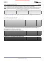
1
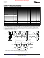
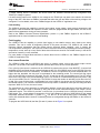
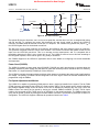
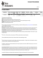
Not Recommended for New Designs
UCD9112
www.ti.com
SLVS711A – SEPTEMBER 2006 – REVISED JUNE 2007
Digital Dual-Phase Synchronous Buck Controller
Check for Samples: UCD9112
FEATURES
APPLICATIONS
•
•
•
•
•
•
•
25 CTRL
26 NC
27 CLK
28 DATA
29 EAN
30 EAP
31 VD33
1
24
CLF2
ADDR0
2
23
CLF1
IOUT_1
3
22
ALERT
VIN
4
21
PGOOD
UCD9112
DPWMA2
TRACK
8
17
SRE2
16
18
FAN_TACH
7
15
TEMP
ILIM
SRE1
14
19
CLF1
6
13
IOUT_2
FAN_PWM
DPWMA1
12
20
AVSS
5
11
VOUT
RST
•
ADDR1
10
•
•
•
•
•
•
•
•
•
•
QFN PACKAGE
(TOP VIEW)
VD25
•
•
•
DC Power Distributed Systems
Industrial / ATE
Networking Equipment
Servers
Storage Systems
Telecommunications Equipment
32 AVSS
•
Digital Dual-Phase Synchronous Buck PWM
Controller With 175ps PWM Resolution
Digital Control With Programmable
Compensation
Dual-Phase With Current Balancing Capability
VOUT from 0.4V to 4.0V
Programmable Switching Frequency,
Capable of up to 1MHz
Programmable Soft Start and Soft Stop
Supports Pre-Biased Start-Up
Supports Voltage Tracking
Supports Remote Differential Voltage Sensing
Supports Fan Speed Adjustment and Monitor
Single 3.3V Bias Supply
Internal and External Thermal Sensor
Fault Logging
Graphical User Interface Configuration
PMBus Support
– Query Voltage, Current, Faults, etc.
– Voltage Setting and Calibration
– Protection Threshold Adjustment
32-Pin QFN Package
9
2
DVSS
1
DESCRIPTION/ORDERING INFORMATION
The UCD9112 is a dual-phase synchronous buck digital PWM controller designed for point of load power
applications. This device integrates dedicated circuitry for DC/DC loop management with a microcontroller core,
flash memory and a PMBus™ interface to support configurability, monitoring and management of a point of load.
The UCD9112 is capable of operating at switching frequencies of up to 1MHz.
The UCD9112 evaluation module comes with the Fusion Digital Power Designer graphical user interface (GUI).
This GUI allows the designer to configure the operating parameters and loop response of the power supply
controller. This configuration can then be stored to the devices on chip non-volatile memory. This will enable a
synchronous buck hardware design to be dynamically calibrated and reconfigured to optimize a single hardware
design for a variety of applications.
The UCD7230 synchronous buck driver has been designed to work with the UCD9112 controller to provide a
highly integrated digital power solution. In addition to 4A output drive capability, the driver integrates current limit,
short circuit protection as well as under-voltage lockout protection. The UCD7230 also has a 3.3V, 10mA linear
regulator that provides the supply current for the controller.
1
2
Please be aware that an important notice concerning availability, standard warranty, and use in critical applications of Texas
Instruments semiconductor products and disclaimers thereto appears at the end of this data sheet.
All trademarks are the property of their respective owners.
PRODUCTION DATA information is current as of publication date.
Products conform to specifications per the terms of the Texas
Instruments standard warranty. Production processing does not
necessarily include testing of all parameters.
Copyright © 2006–2007, Texas Instruments Incorporated
Not Recommended for New Designs
UCD9112
SLVS711A – SEPTEMBER 2006 – REVISED JUNE 2007
www.ti.com
This integrated circuit can be damaged by ESD. Texas Instruments recommends that all integrated circuits be handled with
appropriate precautions. Failure to observe proper handling and installation procedures can cause damage.
ESD damage can range from subtle performance degradation to complete device failure. Precision integrated circuits may be more
susceptible to damage because very small parametric changes could cause the device not to meet its published specifications.
Table 1. ORDERING INFORMATION
(1)
PACKAGE (1)
TAPE AND REEL QUANTITY
PART NUMBER
QFN
3000
UCD9112RHBR
QFN
250
UCD9112RHBT
For the most current package and ordering information, see the Package Option Addendum located at the end of this datasheet or see
the TI website at www.ti.com.
ABSOLUTE MAXIMUM RATINGS (1)
over operating free-air temperature range (unless otherwise noted)
UCD9112
UNIT
VD33 relative to AVSS
PARAMETER
–0.3 to 3.6
V
IO pin relative to DVSS
–0.3 to 3.6
V
Maximum junction temperature, TJ
–40 to 125
°C
Storage temperature, Tstg
–65 to 150
°C
300
°C
Lead temperature (soldering for 10 seconds)
(1)
Stresses beyond those listed under absolute maximum ratings may cause permanent damage to the device. These are stress ratings
only, and functional operation of the device at these or any other conditions beyond those indicated under recommended operating
conditions is not implied. Exposure to absolute-maximum-rated conditions for extended periods may affect device reliability.
RECOMMENDED OPERATING CONDITIONS
over operating free-air temperature range (unless otherwise noted)
MIN
TYP
MAX
UNIT
VD33 relative to AVSS
3.14
3.3
3.46
V
VEAP relative to VEAN
0
2.45
V
–40
125
°C
MAX
UNIT
Operating free-air temperature
ELECTROSTATIC DISCHARGE (ESD) PROTECTION
PARAMETER
MIN
HBM (Human Body Model)
CDM (Charged Device Model)
2
Submit Documentation Feedback
TYP
2000
V
500
V
Copyright © 2006–2007, Texas Instruments Incorporated
Product Folder Link(s): UCD9112
Not Recommended for New Designs
UCD9112
www.ti.com
SLVS711A – SEPTEMBER 2006 – REVISED JUNE 2007
ELECTRICAL CHARACTERISTICS
VD33 = 3.3V, TA = –40°C to 125°C (unless otherwise noted).
PARAMETER
CONDITIONS
MIN
TYP
MAX
3.14
3.3
3.46
4
8
10
UNIT
VDD Input Supply
VD33 supply voltage
Supply current
ICC
Normal operation
VD33 rise time
1
V
mA
ms
VD25
1mF ceramic connected, without
source current
Voltage reference
2.426
2.45
2.475
V
Power on Reset (POR)
Power-on Reset 1
VD33 rising edge
3.0
V
Power-on Reset 2
VD33 falling edge
1.8
V
EAP and EAN
Input differential range
EAP - EAN
EAP bias current
EAP connected to AVSS
EAP bias current
V_EAP = 2.475V
EAN bias current
EAN connected to AVSS
–0.2
2.475
V
–15
mA
30
mA
–10
mA
Error ADC accuracy
±0.5
%
Error ADC resolution
±2.5
mV
1
°C
±3
°C
Internal Temperature Sensor
Resolution
After calibration by adjusting offset
at 25°C
Accuracy
DPWM Output
Duty cycle
0
99
%
Rise time
tr
47pF cap load
15
ns
Fall time
tf
47pF cap load
15
ns
PWM frequency
Fsw
250
Frequency set point accuracy
TA = 25°C
Frequency change
–40 to 125°C
500
1000
±5
±10
kHz
%
%
ILIM Reference Generator
PWM frequency
FILIM
25
Duty cycle range
0
kHz
100
%
0.4
V
Power Good (PGOOD)
Low-level output voltage
VOL
IPGOOD = 5 mA
High-level output voltage
VOH
IPGOOD = –5 mA
Low-level output voltage
VOL
IALERT = 5 mA
High-level output voltage
VOH
IALERT = –5 mA
High input voltage
VIH
VD33 = 3.3V
Low input voltage
VIL
VD33 = 3.3V
Output voltage high
VOH
VD33 = 3.3V, IOH = –5mA
Output voltage low
VOL
VD33 = 3.3V, IOL = 5mA
2.8
V
PMBus Alert
0.4
2.8
V
V
I/O Characteristics
2
3.45
V
0.8
V
2.8
V
0.4
Submit Documentation Feedback
Copyright © 2006–2007, Texas Instruments Incorporated
Product Folder Link(s): UCD9112
V
3
Not Recommended for New Designs
UCD9112
SLVS711A – SEPTEMBER 2006 – REVISED JUNE 2007
www.ti.com
ELECTRICAL CHARACTERISTICS (continued)
VD33 = 3.3V, TA = –40°C to 125°C (unless otherwise noted).
PARAMETER
CONDITIONS
MIN
TYP
MAX
UNIT
PMBus/SMBus
FSMB PMBus/SMBus operating frequency
Slave mode, SMBC 50% duty cycle
100
kHz
Bus free time between start and stop t(BUF)
4.7
ms
Hold time after (repeated) start
t(HD:STA)
4.0
ms
Repeated start setup time
t(SU:STA)
4.7
ms
Stop setup time
t(SU:STO)
4.0
ms
Receive Mode
0
ns
Transmit Mode
300
ns
Data hold time
t(HD:DAT)
Data setup time
t(SU:DAT)
Error signal/detect (1)
t(TIMEOUT)
25
Clock low period
t(LOW)
4.7
t(HIGH)
4.0
Clock high period
(2)
250
ns
35
ms
ms
50
ms
t(LOW:SEXT)
25
ms
Cumulative clock low master extend
time (4)
t(LOW:MEXT)
10
ms
Clock/data fall time (5)
tf
300
ns
Clock/data rise time (6)
tr
1000
ns
Cumulative clock low slave extend
time (3)
(1)
(2)
(3)
(4)
(5)
(6)
The UCD9112 times out when any clock low exceeds t(TIMEOUT).
t(HIGH), Max, is the minimum bus idle time. SMBC = SMBD = 1 for t > 50 ms causes reset of any transaction involving UCD9112 that is
in progress. This specification is valid when the NC_SMB control bit remains in the default cleared state (CLK[0]=0).
t(LOW:SEXT) is the cumulative time a slave device is allowed to extend the clock cycles in one message from initial start to the stop.
t(LOW:MEXT) is the cumulative time a master device is allowed to extend the clock cycles in one message from initial start to the stop.
Fall time tf = 0.9VDD to (VILMAX – 0.15)
Rise time tr = ( VILMAX – 0.15) to (VIHMIN + 0.15)
t(LOW)
tr
t(HD:STA)
tf
SCLK
t(HIGH)
t(HD:STA)
t(HD:DAT)
t(SU:STA)
t(SU:STO)
t(SU:DAT)
SDATA
t(BUF)
P
S
S
Start
P
Stop
t(LOW:SEXT)
SCLKACK
t(LOW:MEXT)
(1)
SCLKACK
(1)
t(LOW:MEXT)
t(LOW:MEXT)
SCLK
SDATA
NOTE: (1) SCLKACK is the acknowledge-related clock pulse generated by the master.
Figure 1. PMBus/SMBus Timing Diagram
4
Submit Documentation Feedback
Copyright © 2006–2007, Texas Instruments Incorporated
Product Folder Link(s): UCD9112
Not Recommended for New Designs
UCD9112
www.ti.com
SLVS711A – SEPTEMBER 2006 – REVISED JUNE 2007
DEVICE INFORMATION
UCD9112 Dual Phase Sync Buck Controller
Feedback Analog
Conditioning
Differential
Sense Input
Digital Error
ADC
Digital
Compensator
Compensator
Configuration 1
Precision
Reference
GPIO
32MHz
Oscillator
High Resolution
DPWM
2 PWM
Outputs
PMBus
Compensator
Configuration 2
Data Bus
6 User Configurable
Channels for Monitoring
▪ Voltage
▪ Current
▪ Temperature
CPU Core
Data Flash
Program
Flash
Figure 2. UCD9112 Block Diagram
Table 2. TERMINAL FUNCTIONS
TERMINAL PIN
DESCRIPTION
NAME
NO.
I/O
A/D
ADDR1
1
I
A
ADDR0
2
I
A
IOUT_1
3
I
A
Phase 1 inductor current, the value is amplified in the UCD7230.
VIN
4
I
A
Input DC voltage sensing through resistors.
VOUT
5
I
A
Output DC voltage sensing through resistors.
IOUT_2
6
I
A
Phase 2 inductor current sensing, the value is amplified in the UCD7230.
ADDR1 and ADDR0 signals are analog voltage inputs that are sampled when the
UCD9112 is released from reset. The voltage levels set the PMBus address that is
used. See the section, PMBus Address Configuration.
TEMP
7
I
A
Temperature remote sensing input.
TRACK
8
I
A
Voltage tracking input.
DVSS
9
-
DG
VD25
10
O
P
Internal 2.5V bypass pin for the UCD9112. A 1mF ceramic cap must be connected
from VD25 to DVSS.
RST
11
I
-
Pulling high resets the chip. Need a pull-down resistor and a 0.1mF decoupling
capacitor.
Digital ground of IC. This ground should be separate from power ground.
AVSS
12
-
AG
FAN_PWM
13
O
D
Connected to analog ground.
Output PWM pulse to drive a fan.
CLF1
14
I
D
Phase 1 over current limit flag from the UCD7230.
ILIM
15
O
D
A PWM ouptut that is used to generate an analog input to the UCD7230 current
limit. The ILIM requires an RC filter consisting of 3.83K and 0.47mF
FAN_TACH
16
I
D
Input pulses from fan tach.
SRE2
17
O
D
Phase 2 Sync FET enable.
DPWMA2
18
O
D
Phase 2 DPWM output to the driver UCD7230.
SRE1
19
O
D
Phase 1 Sync FET enable.
DPWMA1
20
O
D
Phase 1 DPWM output to the driver UCD7230.
PGOOD
21
O
D
Power good signal indicating power conversion status.
ALERT
22
O
D
Alert signal indiating PMBus status.
CLF1
23
I
D
Phase 1 over current limit flag from the UCD7230.
CLF2
24
I
D
Phase 2 over current flag from the UCD7230.
CTRL
25
I
D
ON/OFF command to turn on/off power supply output.
Submit Documentation Feedback
Copyright © 2006–2007, Texas Instruments Incorporated
Product Folder Link(s): UCD9112
5
Not Recommended for New Designs
UCD9112
SLVS711A – SEPTEMBER 2006 – REVISED JUNE 2007
www.ti.com
Table 2. TERMINAL FUNCTIONS (continued)
TERMINAL PIN
6
NAME
NO.
I/O
A/D
DESCRIPTION
NC
26
-
D
Open connection.
CLK
27
I
D
PMBus/SMBus clock input.
DATA
28
I/O
D
PMBus/SMBus data (bi-directional).
EAN
29
I
A
Output voltage remote sensing to error amplifier negative input.
EAP
30
I
A
Output voltage remote sensing to error amplifier positive input.
VD33
31
I
P
3.3V VDD bias supply.
AVSS
32
-
AG
Analog ground.
PAD GND
33
-
Pad
Thermal pad connected to analog ground.
Submit Documentation Feedback
Copyright © 2006–2007, Texas Instruments Incorporated
Product Folder Link(s): UCD9112
Not Recommended for New Designs
UCD9112
www.ti.com
SLVS711A – SEPTEMBER 2006 – REVISED JUNE 2007
APPLICATION INFORMATION
Example Dual-Phase Implementation With the UCD7230 Driver
Vin
12
PVDD
Vout
Vin
18
VDD
CS BIAS
16
5
CLF
CS+
17
19
SRE
OUT1
14
3.3V
UCD9112
RS+
21
1
2
4
5
PGOOD
ADDR1
EAP
EAN
ADDR0
BST
13
OUT2
11
ILIM
SW
15
7
AO
POS
8
1
3V3
NEG
9
3
DLY
PGND
10
20
IN
6
IO
4
30
RS+
29
RS-
VIN
CLF2
24
VOUT
SRE2
17
Iout2
Iout1
3
IOUT_1
6
IOUT_2
32
AVSS
Iout2
DPWMA2
18
ILIM
15
AGND
2
CLF1
Vout
UCD7230
Vin
12
14
PVDD
11
VD33
V_track
RST
SRE1
19
DPWMA1
20
TRACK
CLF1
23
25
CTRL
VD25
10
28
DATA
DVSS
9
31
VD33
8
18
VDD
CS BIAS
16
5
CLF
CS+
17
19
SRE
OUT1
14
UCD7230
20
IN
BST
13
6
IO
OUT2
11
4
ILIM
SW
15
7
AO
POS
8
1
3V3
NEG
9
3
DLY AGND
PGND
10
RS-
PMBus
VD33
27
CLK
22
ALERT
FAN_PWM
FAN_TACH
TEMP
Iout1
16
13
VD33
2
7
RMT
Figure 3. UCD9112 in a Dual Phase Configuration
Submit Documentation Feedback
Copyright © 2006–2007, Texas Instruments Incorporated
Product Folder Link(s): UCD9112
7
Not Recommended for New Designs
UCD9112
SLVS711A – SEPTEMBER 2006 – REVISED JUNE 2007
www.ti.com
FUNCTIONAL OVERVIEW
Reset
Power-on Reset
The UCD9112 has an integrated power-on reset (POR) circuit which monitors the supply voltage. At power-up,
the POR detects the VD33 rise. When VD33 is greater than a predetermined reference point, the device initiates
a startup delay sequence. At the end of the delay sequence, the system reset signal is de-asserted and the
device begins normal operation (See Electrical Characteristics).
External Reset
The device can be forced into the reset state by an external circuit connected to the RST pin. A logic high
voltage on this pin generates a reset signal. To avoid an erroneous trigger caused by the noise, a pull down
resistor and a decoupling capacitor is necessary.
Analog Monitoring
The UCD9112 monitors eight analog signals to determine supply operation. Table 3 shows the analog input pin
assignments.
Table 3. Analog Input Assignment
PIN NO.
PIN NAME
1
ADDR1
Address 1 voltage conversion (for PMBus address configuration)
2
ADDR0
Address 0 voltage conversion (for PMBus address configuration)
3
IOUT_1
Phase 1 current conversion
4
VIN
5
VOUT
6
IOUT_2
7
TEMP
8
TRACK
FUNCTION/DESCRIPTION
POL input voltage conversion
POL output voltage conversion
Phase 2 current conversion
Remote temperature sensing conversion
Voltage tracking reference conversion
The UCD9112 takes the proper actions based on the information acquired from these analog inputs, for example,
turning off the DC output or sending alarm signal to the host system if the output is under voltage. The internal
device temperature is monitored by internal ADC. The status of power supply can be queried any time by the
PMBus master.
Resolution
The UCD9112 uses an internal 2.45V as ADC reference, with a resolution of 2.39mV. The internal reference has
±1% accuracy over temperature. In some applications, an external voltage divider should be used to insure
analog inputs are constrained to a range of zero to 2.45V.
Input Impedance
The input impedance is typically a 250Ω (Rin) series input and a 30pF (CS/H) capacitor to ground. It is
recommended to have a 0.1mF (Cin) input capacitor at each analog input pin. Figure 4 is the equivalent ADC
sampling circuit.
8
Submit Documentation Feedback
Copyright © 2006–2007, Texas Instruments Incorporated
Product Folder Link(s): UCD9112
Not Recommended for New Designs
UCD9112
www.ti.com
SLVS711A – SEPTEMBER 2006 – REVISED JUNE 2007
Rin
SS/H
ADC
Cin
CS/H
Figure 4. Equivalent ADC sampling circuit
PMBus Address Configuration
In order to support multiple POL converters in a system, each converter needs to have the ability to be
configured with unique PMBus address. To configure the UCD9112 with a specific PMBus address, a proper
voltage needs to be applied to the pins ADDR1 and ADDR0. Figure 5 shows what PMBus addresses are
indicated by the applied voltage.
Vaddr
Address not valid when 2.2 V < Vaddr < 3.3 V
2.22
11
2.035
10
1.85
9
1.665
8
1.48
7
1.295
6
1.11
5
0.925
4
0.74
3
0.555
2
0.37
1
0.185
0
Address
Figure 5. VADDR to PMBus Address Translation
Note that the nominal value for each voltage step (and each PMBus address) is in the center of each band.
The address can be represented by the formula:
PMBus_Address = ADDR1 * 12 + ADDR0
Submit Documentation Feedback
Copyright © 2006–2007, Texas Instruments Incorporated
Product Folder Link(s): UCD9112
9
Not Recommended for New Designs
UCD9112
SLVS711A – SEPTEMBER 2006 – REVISED JUNE 2007
www.ti.com
Table 4 lists the examples of the PMBus address for the given voltage level on the ADDR0 and ADDR1.
Table 4. PMBus Address Configurations
ADDR1
ADDR0
PMBus Address
ADDR1
ADDR0
PMBus Address
<0.185
<0.185
0x00
0.185-0.37
<0.185
0x0C
0.185-0.37
0x01
0.185-0.37
0x0D
0.37-0.555
0x02
0.37-0.555
0x0E
0.555-0.74
0x03
0.555-0.74
0x0F
0.74-0.925
0x04
0.74-0.925
0x10
0.925-1.11
0x05
0.925-1.11
0x11
1.11-1.295
0x06
1.11-1.295
0x12
1.295-1.48
0x07
1.295-1.48
0x13
1.48-1.665
0x08
1.48-1.665
0x14
1.665-1.85
0x09
1.665-1.85
0x15
1.85-2.035
0x0A
1.85-2.035
0x16
2.035-2.22
0x0B
2.035-2.22
0x17
The other addresses can be figured out by using the above formula. If the voltage applied on the address pins is
over 2.22V, it is decoded as 127; or if both address pins are connected to ground, the PMBus address is
decoded as 127.
PID Compensator
The UCD9112 has a digital voltage mode controller, or compensator, that has been implemented in digital PID
format. This PID compensator allows output voltage regulation at the set point reference level with zero steady
state error and good dynamic performance. The integrator in the PID compensator results in the high DC gain in
the control loop and thereby maintains the zero steady state error. In the complex s-plane, the PID compensator
transfer function shows a single pole at s=0, two adjustable compensator zeros and an adjustable gain factor.
For good dynamic performance of the power supply output, the power supply designer needs to properly select
these compensator zeros and the gain factor in order to achieve acceptable loop bandwidth with optimum phase
and gain margin. The graphical user interface (GUI) provided with the UCD9112 allows the designer an easy way
to select these PID parameters and verify the control loop design by reviewing the loop gain Bode plots. Once a
control loop design looks acceptable, the GUI calculates the coefficients of the digital PID compensator and
generates the compensator coefficients. These coefficients can then be stored in the UCD9112’s non-volatile and
operating memory.
The synchronous buck topology is commonly used for non-isolated DC/DC converters. The choice of PID
compensator gain and zeros are determined by the power stage parameters such as input voltage, PWM
frequency, output filter inductor, capacitor, and the parasitic components. In the traditional analog power supply
design, an operational error amplifier and external compensation components are used to implement the
compensator. For the UCD9112, this is achieved by using the on-chip error ADC (EADC) and the look-up table
based PID compensator. In this case, the output voltage is first scaled and filtered appropriately before applying
it into the UCD9112 EADC. The EADC output is used by the UCD9112 on-chip PID compensator in order to
generate a control signal for use in the DPWM module. The DPWM module finally generates the required PWM
outputs for the buck converter switches based on the PID compensator control output.
10
Submit Documentation Feedback
Copyright © 2006–2007, Texas Instruments Incorporated
Product Folder Link(s): UCD9112
Not Recommended for New Designs
UCD9112
www.ti.com
SLVS711A – SEPTEMBER 2006 – REVISED JUNE 2007
Output Voltage Remote Sensing
Figure 6 shows the voltage sensing circuitry for the UCD9112. It is part of feedback loop. Two dedicated pins,
EAP and EAN, are employed to sense the output differential voltage. The differential voltage sensing can
effectively reduce the common-mode noise. The maximum voltage applied on the VEAP and VEAN pins should
be less than 2.45V. If the output voltage is higher than 2.45V, a voltage divider should be used to decrease the
voltage level applied to the pin below 2.45V to avoid error ADC saturation.
Vin
Phase 1
SW1
L
Vout
SW2
R1
C
EAP
PGND
R2
EAN
Phase 2
AVSS
UCD9112
PGND
AGND
Figure 6. Output Voltage Sensing Circuitry
OTHER FUNCTIONS
Output Enable
The UCD9112 can be configured to begin power conversion in the following ways:
1. As soon as it detects sufficient input voltage;
2. As soon as it detects sufficient input voltage and the Control line is toggled to active state by a
HOST/Sequencer;
3. As soon as it detects sufficient input voltage and the relevant PMBus command is received.
This feature is configurable and is supported by a combination of the PMBus commands and the state of the
Control signal. For more details, refer to the “PMBus Support for the UCD911X” application note.
Input Voltage Calibration
The UCD9112 periodically monitors the input voltage. The PMBus master can read the input voltage value by a
PMBus command. In most applications, the input voltage is connected to the VIN pin using an external voltage
divider. The voltage level is lowered to match the device’s internal ADC input voltage range. To compensate for
the tolerances of this voltage divider, the input voltage monitoring path might need to be calibrated. This input
voltage calibration is performed by adjusting the input voltage monitoring scale (VIN_SCALE_MONITOR) value
using the relevant PMBus command. For more details, refer to the “PMBus Support for the UCD911X”
application note.
Output Voltage Calibration
Similar to the input voltage connection, the output voltage may be connected to the UCD9112 through an
external voltage divider. The output voltage level may need to be scaled to match the device’s ADCs (Error ADC
and 10bit-ADC) input voltage ranges using two independent voltage dividers.
Submit Documentation Feedback
Copyright © 2006–2007, Texas Instruments Incorporated
Product Folder Link(s): UCD9112
11
Not Recommended for New Designs
UCD9112
SLVS711A – SEPTEMBER 2006 – REVISED JUNE 2007
www.ti.com
1. One of the voltage dividers may be used to connect the output voltage to the EAP pin. This path is used to
close the compensation loop and provides the high-speed Error-ADC with the required feedback signal. To
compensate for the tolerances of this voltage divider, the calibration of loop scale calibration is required.
Loop scale calibration is performed by adjusting the loop scale value using the VOUT_SCALE_LOOP
PMBus command.
2. The second voltage divider may be used to connect the output voltage to the VOUT pin. This path is used to
monitor the output voltage and provides the 10bit-ADC with the required signal for fault detection and output
voltage reporting purposes. To compensate for the tolerances of this voltage divider, the output voltage
monitor scale calibration is required. The output voltage monitoring signal calibration is performed by
adjusting the monitoring scale value using the VOUT_SCALE_MONITOR PMBus command.
In addition, the output voltage may be trimmed using the VOUT_TRIM command. For more details, refer to the
“PMBus Support for the UCD911X” application note.
Output Current Calibration
The UCD9112 can measure the current from each phase via the UCD7230 gate driver. The measurement of the
inductor current for each phase is made by measuring a voltage equivalent to the voltage across the DCR of
each output inductor shown in Figure 7.
L
DCR
C
R
I_sense
Figure 7. Inductor Current Sensing Circuit
The voltage across the inductor’s DCR is the equal to the voltage across capacitor C if the time constant of
L/DCR = RC is met. Slight mismatch in the time constants only affects measured accuracy during transients. The
DC value of the voltage on the C will always track the DC value of the voltage on the DCR. This voltage is
measured and amplified by the UCD7230 gate driver and reported to the UCD9112 via the IOUT_1 or IOUT_2
analog inputs, depending on the phase. The UCD9112 calculates the total current by the addition of two phase
currents. Each phase current is calculated by the formula:
IOUT_X = Offset_X = Gain_X * I_sense_X
Where: X represents the phase number.
These calibration parameters can be different on each phase due to tolerances of the selected components. The
current measurements are calibrated by adjusting the offset and gain of the phase current inputs through the
PMBus. The gain term includes the gain of the UCD7230 differential amplifier and the value of the inductor DCR.
The DCR value is assumed to have a temperature coefficient of copper. The DCR value is compensated by the
temperature value reported by the external temperature sensor. I_sense is the voltage across the DCR. A current
amplifier built in the UCD7230 is used to amplify this voltage for the UCD9112. For more details on configuration
of the gain and offset for current measurement, refer to the “PMBus Support for the UCD911X” application note.
Phase Current Balancing
The UCD9112 is a dual-phase synchronous buck PWM controller. Each phase is driven by a UCD7230 gate
driver. Each UCD7230 gate driver includes a differential amplifier for inductor current sensing. This value is also
offset so that bidirectional current can be measured. The analog value is output on the A0 pin of the UCD7230.
The UCD9112 uses two pins, IOUT_1 and IOUT_2, to sense the phase currents from each UCD7230. Since the
components in each phase are different, each of the phase currents can be different when provided with the
12
Submit Documentation Feedback
Copyright © 2006–2007, Texas Instruments Incorporated
Product Folder Link(s): UCD9112
Not Recommended for New Designs
UCD9112
www.ti.com
SLVS711A – SEPTEMBER 2006 – REVISED JUNE 2007
same duty-cycle. The UCD9112 performs phase current balancing during regulation when both phases are
enabled. It is implemented by adjusting the individual phase duty-cycles so that each phase can have matching
inductor current. The current difference between two phases is within 5% of load current when output current is
over 50% of full load. There is no current balancing implemented in the UCD9112 if the load current is less than
2A.
Output Sequencing
The UCD9112 supports output voltage sequencing. Sequencing can be implemented by configuring each
individual power supply with a different turn-on-delay (TON_DELAY), rise-time (TON_RISE), turn-off-delay
(TOFF_DELAY), and fall-time (TOFF_FALL) values. During sequencing, each power supply unit supplies power
to a separate voltage rail and all power supply units are commanded to turn their output on (or off)
simultaneously by a single via the PMBus Control line or group command. All the above parameters are
configurable using PMBus commands. This allows a user to implement different sequencing scenarios such as
Sequential, Ratiometric, Simultaneous, etc. For more details, refer to the “PMBus Support for the UCD911X”
application note.
Soft-start and Soft-stop
The UCD9112 supports soft-start and soft-stop functionality. The turn-on-delay (TON_DELAY), rise-time
(TON_RISE), turn-off-delay (TOFF_DELAY), and fall-time (TOFF_FALL) values are configurable using PMBus
commands. These parameters are specified in milli-seconds, and have a range of zero to 255 milliseconds. The
UCD9112 doesn’t support soft-stop at light load. Output voltage is turned off directly and there is no soft-stop if
load current is less than 2AThe Figure 8 illustrates the four time intervals in the soft-start/stop sequence.
Control
Rise Time
Output
Voltage
(Vout)
Turn Off Delay
Maximum Pre-bias level; 75% of Vout
Turn On Delay
SRE
Modulation
Fall Time
Figure 8. Soft start/stop timings and SRE modulation
Submit Documentation Feedback
Copyright © 2006–2007, Texas Instruments Incorporated
Product Folder Link(s): UCD9112
13
Not Recommended for New Designs
UCD9112
SLVS711A – SEPTEMBER 2006 – REVISED JUNE 2007
www.ti.com
SRE Modulation
The UCD9112 supports output voltage ramp up and ramp down, even when a voltage is already present at the
output terminals. This voltage which is persistent even when the device’s output is off is commonly referred to as
pre-bias voltage. Under typical circumstances, the power supply start-up (or shut-down) should not affect the
pre-bias voltage and the output stage switches should not draw (sink) current. In order to avoid current sink via
the lower FET (SYNC-FET), UCD7230’s SRE pin is turned off by the UCD9112 controller.
Since turning SYNC-FET on and off during the operation has adverse effect on output voltage (causes
transients), the UCD9112 turns SYNC-FET on and off gradually by varying (increasing or decreasing) the pulse
width of the signal connected to the UCD7230’s SRE pin.
In start-up (soft-start) scenario, the SRE is kept in off position as long as the output voltage is lower than the
maximum possible pre-bias voltage level (75% of the configured output voltage set point). When the maximum
pre-bias voltage is crossed, the UCD9112 gradually turns on the SRE signal. This is done by gradually
increasing the pulse width of the PWM signal generated specifically for this purpose.
In shut-down (soft-stop) scenario, the SRE is switched to off position before the output voltage gets lower than
the maximum possible pre-bias voltage level. Before the maximum pre-bias voltage is crossed, the UCD9112
gradually turns off the SRE signal. This is done by gradually decreasing the pulse width of the PWM signal
generated specifically for this purpose.
The SRE modulation does not happen during the lower 75% of ramp-up and the lower 75% of ramp-down time
intervals. Therefore, for proper start-up (or shut-down) into pre-bias, the pre-bias voltage can not be more than
75% of the configured output voltage set point. Figure 5-2 illustrates SRE modulation time intervals in the
soft-start/stop sequence.
Start-up with Pre-bias
The UCD9112 supports soft-start with existing pre-bias output voltage. When the output is enabled, the
UCD9112 checks the output for the presence of pre-bias voltage. The UCD9112 reacts to pre-bias voltage level
as follows:
If (Prebias < Prebias_min (300 mV default)), the start-up is performed assuming no pre-bias. The device
proceeds through standard soft-delay/soft-start sequence.
If (Prebias > Prebias_max (3.65 V default)), the device does not attempt start-up and reports the specific
fault in the status registers.
If (Prebias > output voltage set point), the device ramps down the output voltage to the output voltage set
point.
If (Prebias < output voltage set point), the device ramps up the output voltage to the output voltage set point.
Voltage Tracking
The UCD9112 supports output voltage tracking by following the voltage on its TRACK pin. This feature can be
enabled or disabled by the TRACKING_ENABLE. By default, the feature is disabled.
The voltage on the TRACK pin is referred as a parent’s voltage, and is usually driven by another power supply
referred as the parent or master device. When the tracking power supply (the UCD9112 in this case) is
commanded to startup, the output voltage starts to track the parent’s voltage.
The voltage tracking starts only when the voltage on the TRACK pin is greater than 300mV and ends when the
UCD9112’s output voltage reaches its configured output voltage level that is specified by VOUT_COMMAND.
During tracking, the UCD9112’s output follows the parent’s output with an accuracy of ±100mV. The UCD9112 is
capable of following the parent's voltage slew rates of up to 100mV/ms. If the parent’s voltage drops below the
commanded output voltage, the UCD9112 will follow the parent's voltage down to at least 300mV.
If the device is requested to shut down through any legal combination of the OPERATION command and/or the
CONTROL line, then it performs soft-stop according to PMBus configuration (by following TOFF_DELAY and
TOFF_FALL timings).
If any fault condition causes the output to shutdown, then the converter turns the output off according to the fault
configuration.
If the parent supply is turned on before the tracking device is commanded to start tracking, then the tracking
device will either reach its VOUT_COMMAND voltage or the parent’s output voltage; whichever is lower.
14
Submit Documentation Feedback
Copyright © 2006–2007, Texas Instruments Incorporated
Product Folder Link(s): UCD9112
Not Recommended for New Designs
UCD9112
www.ti.com
SLVS711A – SEPTEMBER 2006 – REVISED JUNE 2007
If voltage tracking feature is disabled, the device follows the standard soft-start/soft-stop configuration and
TRACK pin voltage is ignored.
Like other analog inputs on the UCD9112, the voltage on the TRACK pin may have to be scaled to fit within the
range of the ADC, and there are PMBus commands that allow the gain and offset of the tracking voltage to be
configured. For more details, refer to the “PMBus Support for the UCD911X” application note.
Fault Handling
The UCD9112 provides the capability to monitor input voltage, output voltage, output current, temperature, and
fan speed. These thresholds and responses to these faults are programmable through PMBus, as well as the
status of these parameters during converter operation.
Refer to the PMBus Command Protocol Specification (version 1.1) and “PMBus Support for the UCD911X”
application note for more information on fault handling.
Fault Logging
The UCD9112 has the capability to provide fault logging to non-volatile memory when faults occur during
operation. This can be useful for diagnosing failures of the power converter. The UCD9112 will record the
maximum lifetime temperature that the remote sensor observed during operation, once it crosses the
over-temperature warning limit. The UCD9112 will also record the reason for any operating fault as well (voltage,
temperature, current, start-up or fan). Both of these sets of faults are stored in non-volatile memory in the device
and can be cleared by a user command.
For more details on logged faults and how to retrieve them from the UCD9112, see “PMBus Support for the
UCD911X” application note.
Over-current Protection
The UCD9112 works with the UCD7230 gate driver to measure output current and provide output current
protection. The UCD9112 and UCD7230 system provides three levels of over-current protection.
First, cycle-by-cycle current is monitored in the UCD7230 by sensing the current of top MOSFET. A current limit
threshold can be configured through external resistors on the CS+ and CSBIAS inputs to the UCD7230 (See the
UCD7230 data sheet for more information). The MOSFET current is compared to the current threshold and if it is
higher than the threshold, the duty-cycle is terminated for the remaining period. The current limit flag output
(CLF) of the UCD7230 is become a logic high. The CLF is kept high for the next switching cycle. The CLF will be
reset at the rising edge of the second switching cycle if over current is not detected during the next period. If the
over current remains, the CLF remains high. The UCD9112 counts the number of switching cycles when the CLF
is high. If the count is higher than a configurable limit in the UCD9112, the device can be configured to shut off
the DPWM outputs. The converter would then enter hiccup mode or latched-off mode per the configured fault
response. When CLF is low, the count is reset.
The second level of current protection is configurable (both the current limit and what to do when that limit is
exceeded). The output current is obtained by using the DCR current method described in the Output Current
Calibration section. The UCD9112 provides a current limit (ILIM) threshold for the UCD7230 through a filtered
PWM output. The I_sense voltage is compared to VLIM/10 (the voltage on ILIM pin of UCD7230) by a high speed
comparator inside the UCD7230. If I_sense > VLIM /10, the CLF is set and the duty-cycle is terminated. The
current limit threshold and the number of switching pulses are configurable through the PMBus on the UCD9112
controller.
To program the UCD7230 ILIM, the filter (R1 and C1) shown in the Figure 9 is required.
Submit Documentation Feedback
Copyright © 2006–2007, Texas Instruments Incorporated
Product Folder Link(s): UCD9112
15
Not Recommended for New Designs
UCD9112
SLVS711A – SEPTEMBER 2006 – REVISED JUNE 2007
www.ti.com
VLIM
R1=3.83K
ILIM
3.3V
UCD7230
UCD9112
UCD7230
3.3V
R2=280K
ILIM
R2=280 K
ILIM
R3=50K
U3
C1=0.47uF
U1
R3=50K
U2
Figure 9. RC filter used for ILIM
The resistor R1 has two functions, one is to form a low pass filter, and the other is to form a voltage divider along
with R2 and R3. To configure the current limit threshold, the user simply needs to instruct the UCD9112
controller via PMBus what the desired current limit is in amperes. The controller will generate the proper VLIM to
the UCD7230 gate driver for the desired current limit.
The last level of over-current protection is provided by the UCD9112 and uses average current for protection.
This protection responds slower but can be more accurate. The UCD9112 monitors each phase current from an
input from the UCD7230 gate driver. This is an average current measurement, and it is compared with a
threshold to determine if there is over current fault or not. The UCD9112 will then act on this fault according to
the configured response, which can be ignore, retry, delay or shutdown.
See “PMBus Support for the UCD911X” application note for more details on configuring over-current thresholds
and responses.
Power Good (PGOOD)
The UCD9112 supports a power good signal (PGOOD). PGOOD can notify other devices or the host about the
operating condition of power supply at a fast speed in order that necessary actions should be taken to avoid any
data losses. It is implemented by PGOOD pin of the UCD9112.
The UCD9112 monitors the output voltage, and then either asserts or de-asserts the power good signal based on
the voltage. The polarity of PGOOD can be configured to be active high or active low and the threshold can be
programmed using the PMBus.
Fan Speed Adjustment and Monitor
The UCD9112 is capable of generating PWM pulses to drive a single fan installed in the system. The fan PWM
(FFAN) frequency generated by the UCD9112 is fixed at about 700Hz. The fan speed can be varied by adjusting
the average supplied voltage to the fan which in turn can be adjusted by changing the duty cycle. Thus, the
PMBus master can control the fan speed by issuing the relevant PMBus command. The fan’s TACH output
needs to be connected to FAN_TACH input pin of UCD9112 for fan speed monitoring. The PMBus master can
query the fan speed (in RPM) by issuing the relevant PMBus command. The number of pulses per revolution is
configurable. The UCD9112 supports 8 different fan speeds as listed in the Table 5.
16
Submit Documentation Feedback
Copyright © 2006–2007, Texas Instruments Incorporated
Product Folder Link(s): UCD9112
Not Recommended for New Designs
UCD9112
www.ti.com
SLVS711A – SEPTEMBER 2006 – REVISED JUNE 2007
Table 5. FAN duty cycle commands
COMMANDED FAN DUTY
CYCLE
ACTUAL FAN DUTY CYCLE
0% to 7%
0%
8% to 21%
14.3%
22% to 35%
28.6%
36% to 50%
43%
51% to 64%
57%
65% to 78%
71.4%
79% to 92%
85.7%
93% to 100%
100%
If the fan’s actual speed falls below the configured FAN_SPEED_FAULT_LIMIT, the fan fault is generated and
the relevant status registers get updated accordingly.
For more details, refer to the “PMBus Support for the UCD911X” application note.
Light Load Efficiency Optimization
A dual phase power supply has several advantages over a single phase supply. The two major advantages are
improved efficiency and lower output ripple.
Though a dual phase power supply has better efficiency for a typical or heavy load, it actually offers lower
efficiency for lighter loads. The UCD9112 allows phase shedding in order to boost back the efficiency at lighter
loads. The PMBus master can set the UCD9112 into light load mode by a PMBus command. In light load mode,
only one phase is operational. Due to this, switching losses are cut into half and efficiency improves.
By default, the light load mode is disabled. For more details, refer to the “PMBus Support for the UCD911X”
application note
Remote Temperature Sensing
The UCD9112 has support for internal and remote temperature sensing. The internal temperature sensor
requires no calibration and can report the device temperature via the PMBus interface. See “PMBus Support for
the UCD911X” application note on the PMBus command to access the internal temperature sensor.
The remote temperature sensor can report the remote temperature by using a configurable gain and offset for
the type of sensor that is used in the application (P-N junction or a linear temperature sensor (LTS). The
UCD9112 allows warning and fault thresholds to be configured for under and over-temperature based on the
remote temperature (and not the internal sensor). Both the configurable thresholds as well as the reported
temperature are available via the PMBus interface on the device. See “PMBus Support for the UCD911X”
application note for more details.
The remote temperature is sensed through the TEMP pin of the device. A LTS or a P-N junction can be used for
the temperature sensor. A thermistor can be configured to provide a somewhat linear response over a narrow
range of temperatures. It may be acceptable in some applications to use a thermistor where the response has
been linearized near the warning and fault thresholds. A P-N junction has an advantage of lower cost and a
linear response to temperature changes. The UCD9112 uses a P-N junction on its evaluation module (EVM) to
sense the temperature. It is located close to the inductor so that the inductor’s temperature can be sensed. It is
used for temperature protection as well as DCR compensation. The gain and offset of P-N junction can be
configured through the PMBus to calibrate the sensor. Since the gain and offset are the only variables that are
configurable to report the temperature, it is advised to use a sensor that is relatively linear over the range of
interest.
Configuration Security
The UCD9112 provides a configuration security mechanism to allow the user to protect the configuration from
unwanted changes. The device can be configured so that only an administrator will be permitted to make the
changes by entering a password and specifying which parameters users should be allowed to change via
PMBus.
Submit Documentation Feedback
Copyright © 2006–2007, Texas Instruments Incorporated
Product Folder Link(s): UCD9112
17
Not Recommended for New Designs
UCD9112
SLVS711A – SEPTEMBER 2006 – REVISED JUNE 2007
www.ti.com
For complete details on the capabilities and usage of Configuration Security, refer to the PMBus Security
Application Note.
GRAPHICAL USER INTERFACE
All TI digital controllers come with a Graphical User Interface (GUI) that supports configuration, monitoring and
design of any power converter built with the UCD9K family of digital controllers.
The key functions of the GUI for the UCD9112 are listed below:
• PID coefficients programming
• POL ON/OFF
• Voltage and current calibration
• POL parameter configuration
• Read output voltage, output current, temperature
• Fault threshold configuration
• Manufacturing information storage
In addition to the above, the GUI assists users with the design of their power converters using the UCD9112 and
UCD7230 gate driver. The design portion of the GUI allows users to simulate and model the plant, digital
compensator and loop response in both the Continuous and Discrete domains. The GUI can also help generate
the digital compensator loop coefficients and save them as a project file in your PC, and send them to the device
via the PMBus for evaluation and testing.
For more information on the capabilities of the GUI, please see the Fusion Digital Power Designer User Manual.
18
Submit Documentation Feedback
Copyright © 2006–2007, Texas Instruments Incorporated
Product Folder Link(s): UCD9112
Not Recommended for New Designs
UCD9112
www.ti.com
SLVS711A – SEPTEMBER 2006 – REVISED JUNE 2007
APPENDIX A
Table 6. List of Acronyms in the Datasheet
ACRONYM
DESCRIPTION
POL
Point of load
AG
Analog ground
DG
Digital ground
POR
Power on reset
Tj
Junction temperature
Tsj
Storage temperature
tr
Rise time
tf
Fall time
Fsw
PWM switching frequency
FFAN
Fan drive PWM frequency
VOL
Low level output voltage
VOH
High level output voltage
VIL
Low level input voltage
VIH
High level input voltage
Vout
Output voltage
Vin
Input voltage
Iout
Output current
CLF
Current limit flag
I_sense
VLIM
Current sensing voltage
Voltage on the ILIM pin of UCD7230
A
Analog
D
Digital
P
Power
VD33
3.3V supply for the device
ICC
Bias current for the device
VILMAX
Maximum input low level voltage
VIHMIN
Minimum input high level voltage
Rin
ADC input impedance
Cin
External input capacitor
SS/H
ADC sampling and hold switch
CS/H
ADC sampling and hold capacitor
PID
Proportional-integral-derivative
GUI
Graphic user interface
EADC
Error ADC
Vaddr
Voltage on ADDR0 or ADDR1 pin
T_Rise
Output rise time
T_Fall
Output fall time
SRE
Synchronous rectifier enable
FILIM
PWM frequency for ILIM
REFERENCES
• PMBus Support in UCD911x Family of Digital Power Controllers - SLUA427
• Configuration Security for UCD91xx Digital Controllers - SLUA428
Submit Documentation Feedback
Copyright © 2006–2007, Texas Instruments Incorporated
Product Folder Link(s): UCD9112
19
PACKAGE OPTION ADDENDUM
www.ti.com
2-Oct-2014
PACKAGING INFORMATION
Orderable Device
Status
(1)
UCD9112RHBT
NRND
Package Type Package Pins Package
Drawing
Qty
VQFN
RHB
32
250
Eco Plan
Lead/Ball Finish
MSL Peak Temp
(2)
(6)
(3)
Green (RoHS
& no Sb/Br)
CU NIPDAU
Level-2-260C-1 YEAR
Op Temp (°C)
Device Marking
(4/5)
-40 to 85
UCD
9112
(1)
The marketing status values are defined as follows:
ACTIVE: Product device recommended for new designs.
LIFEBUY: TI has announced that the device will be discontinued, and a lifetime-buy period is in effect.
NRND: Not recommended for new designs. Device is in production to support existing customers, but TI does not recommend using this part in a new design.
PREVIEW: Device has been announced but is not in production. Samples may or may not be available.
OBSOLETE: TI has discontinued the production of the device.
(2)
Eco Plan - The planned eco-friendly classification: Pb-Free (RoHS), Pb-Free (RoHS Exempt), or Green (RoHS & no Sb/Br) - please check http://www.ti.com/productcontent for the latest availability
information and additional product content details.
TBD: The Pb-Free/Green conversion plan has not been defined.
Pb-Free (RoHS): TI's terms "Lead-Free" or "Pb-Free" mean semiconductor products that are compatible with the current RoHS requirements for all 6 substances, including the requirement that
lead not exceed 0.1% by weight in homogeneous materials. Where designed to be soldered at high temperatures, TI Pb-Free products are suitable for use in specified lead-free processes.
Pb-Free (RoHS Exempt): This component has a RoHS exemption for either 1) lead-based flip-chip solder bumps used between the die and package, or 2) lead-based die adhesive used between
the die and leadframe. The component is otherwise considered Pb-Free (RoHS compatible) as defined above.
Green (RoHS & no Sb/Br): TI defines "Green" to mean Pb-Free (RoHS compatible), and free of Bromine (Br) and Antimony (Sb) based flame retardants (Br or Sb do not exceed 0.1% by weight
in homogeneous material)
(3)
MSL, Peak Temp. - The Moisture Sensitivity Level rating according to the JEDEC industry standard classifications, and peak solder temperature.
(4)
There may be additional marking, which relates to the logo, the lot trace code information, or the environmental category on the device.
(5)
Multiple Device Markings will be inside parentheses. Only one Device Marking contained in parentheses and separated by a "~" will appear on a device. If a line is indented then it is a continuation
of the previous line and the two combined represent the entire Device Marking for that device.
(6)
Lead/Ball Finish - Orderable Devices may have multiple material finish options. Finish options are separated by a vertical ruled line. Lead/Ball Finish values may wrap to two lines if the finish
value exceeds the maximum column width.
Important Information and Disclaimer:The information provided on this page represents TI's knowledge and belief as of the date that it is provided. TI bases its knowledge and belief on information
provided by third parties, and makes no representation or warranty as to the accuracy of such information. Efforts are underway to better integrate information from third parties. TI has taken and
continues to take reasonable steps to provide representative and accurate information but may not have conducted destructive testing or chemical analysis on incoming materials and chemicals.
TI and TI suppliers consider certain information to be proprietary, and thus CAS numbers and other limited information may not be available for release.
In no event shall TI's liability arising out of such information exceed the total purchase price of the TI part(s) at issue in this document sold by TI to Customer on an annual basis.
Addendum-Page 1
Samples
PACKAGE OPTION ADDENDUM
www.ti.com
2-Oct-2014
Addendum-Page 2
PACKAGE MATERIALS INFORMATION
www.ti.com
18-Aug-2014
TAPE AND REEL INFORMATION
*All dimensions are nominal
Device
UCD9112RHBT
Package Package Pins
Type Drawing
VQFN
RHB
32
SPQ
250
Reel
Reel
A0
Diameter Width (mm)
(mm) W1 (mm)
180.0
12.4
Pack Materials-Page 1
5.3
B0
(mm)
K0
(mm)
P1
(mm)
5.3
1.5
8.0
W
Pin1
(mm) Quadrant
12.0
Q2
PACKAGE MATERIALS INFORMATION
www.ti.com
18-Aug-2014
*All dimensions are nominal
Device
Package Type
Package Drawing
Pins
SPQ
Length (mm)
Width (mm)
Height (mm)
UCD9112RHBT
VQFN
RHB
32
250
210.0
185.0
35.0
Pack Materials-Page 2
IMPORTANT NOTICE
Texas Instruments Incorporated and its subsidiaries (TI) reserve the right to make corrections, enhancements, improvements and other
changes to its semiconductor products and services per JESD46, latest issue, and to discontinue any product or service per JESD48, latest
issue. Buyers should obtain the latest relevant information before placing orders and should verify that such information is current and
complete. All semiconductor products (also referred to herein as “components”) are sold subject to TI’s terms and conditions of sale
supplied at the time of order acknowledgment.
TI warrants performance of its components to the specifications applicable at the time of sale, in accordance with the warranty in TI’s terms
and conditions of sale of semiconductor products. Testing and other quality control techniques are used to the extent TI deems necessary
to support this warranty. Except where mandated by applicable law, testing of all parameters of each component is not necessarily
performed.
TI assumes no liability for applications assistance or the design of Buyers’ products. Buyers are responsible for their products and
applications using TI components. To minimize the risks associated with Buyers’ products and applications, Buyers should provide
adequate design and operating safeguards.
TI does not warrant or represent that any license, either express or implied, is granted under any patent right, copyright, mask work right, or
other intellectual property right relating to any combination, machine, or process in which TI components or services are used. Information
published by TI regarding third-party products or services does not constitute a license to use such products or services or a warranty or
endorsement thereof. Use of such information may require a license from a third party under the patents or other intellectual property of the
third party, or a license from TI under the patents or other intellectual property of TI.
Reproduction of significant portions of TI information in TI data books or data sheets is permissible only if reproduction is without alteration
and is accompanied by all associated warranties, conditions, limitations, and notices. TI is not responsible or liable for such altered
documentation. Information of third parties may be subject to additional restrictions.
Resale of TI components or services with statements different from or beyond the parameters stated by TI for that component or service
voids all express and any implied warranties for the associated TI component or service and is an unfair and deceptive business practice.
TI is not responsible or liable for any such statements.
Buyer acknowledges and agrees that it is solely responsible for compliance with all legal, regulatory and safety-related requirements
concerning its products, and any use of TI components in its applications, notwithstanding any applications-related information or support
that may be provided by TI. Buyer represents and agrees that it has all the necessary expertise to create and implement safeguards which
anticipate dangerous consequences of failures, monitor failures and their consequences, lessen the likelihood of failures that might cause
harm and take appropriate remedial actions. Buyer will fully indemnify TI and its representatives against any damages arising out of the use
of any TI components in safety-critical applications.
In some cases, TI components may be promoted specifically to facilitate safety-related applications. With such components, TI’s goal is to
help enable customers to design and create their own end-product solutions that meet applicable functional safety standards and
requirements. Nonetheless, such components are subject to these terms.
No TI components are authorized for use in FDA Class III (or similar life-critical medical equipment) unless authorized officers of the parties
have executed a special agreement specifically governing such use.
Only those TI components which TI has specifically designated as military grade or “enhanced plastic” are designed and intended for use in
military/aerospace applications or environments. Buyer acknowledges and agrees that any military or aerospace use of TI components
which have not been so designated is solely at the Buyer's risk, and that Buyer is solely responsible for compliance with all legal and
regulatory requirements in connection with such use.
TI has specifically designated certain components as meeting ISO/TS16949 requirements, mainly for automotive use. In any case of use of
non-designated products, TI will not be responsible for any failure to meet ISO/TS16949.
Products
Applications
Audio
www.ti.com/audio
Automotive and Transportation
www.ti.com/automotive
Amplifiers
amplifier.ti.com
Communications and Telecom
www.ti.com/communications
Data Converters
dataconverter.ti.com
Computers and Peripherals
www.ti.com/computers
DLP® Products
www.dlp.com
Consumer Electronics
www.ti.com/consumer-apps
DSP
dsp.ti.com
Energy and Lighting
www.ti.com/energy
Clocks and Timers
www.ti.com/clocks
Industrial
www.ti.com/industrial
Interface
interface.ti.com
Medical
www.ti.com/medical
Logic
logic.ti.com
Security
www.ti.com/security
Power Mgmt
power.ti.com
Space, Avionics and Defense
www.ti.com/space-avionics-defense
Microcontrollers
microcontroller.ti.com
Video and Imaging
www.ti.com/video
RFID
www.ti-rfid.com
OMAP Applications Processors
www.ti.com/omap
TI E2E Community
e2e.ti.com
Wireless Connectivity
www.ti.com/wirelessconnectivity
Mailing Address: Texas Instruments, Post Office Box 655303, Dallas, Texas 75265
Copyright © 2014, Texas Instruments Incorporated