1
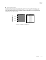
Cover
MICROCOMPUTER
MN101C
MN101C78A/F78A
LSI User’s Manual
Pub.No.21478-013E
Special Attention and Precautions
PanaXSeries is a trademark of Matsushita Electric Industrial Co., Ltd.
The other corporation names, logotype and product names written in this book are trademarks or registered trademarks of their
corresponding corporations.
Request for your special attention and precautions in using the technical information
and semiconductors described in this book
(1) An export permit needs to be obtained from the competent authorities of the Japanese Government if any of
the products or technologies described in this book and controlled under the "Foreign Exchange and Foreign
Trade Law" is to be exported or taken out of Japan.
(2) The technical information described in this book is limited to showing representative characteristics and
applied circuits examples of the products. It neither warrants non-infringement of intellectual property right
or any other rights owned by our company or a third party, nor grants any license.
(3) We are not liable for the infringement of rights owned by a third party arising out of the use of the product or
technologies as described in this book.
(4) The products described in this book are intended to be used for standard applications or general electronic
equipment (such as office equipment, communications equipment, measuring instruments and household
appliances).
Consult our sales staff in advance for information on the following applications:
• Special applications (such as for airplanes, aerospace, automobiles, traffic control equipment, combustion
equipment, life support systems and safety devices) in which exceptional quality and reliability are required,
or if the failure or malfunction of the products may directly jeopardize life or harm the human body.
• Any applications other than the standard applications intended.
(5) The products and product specifications described in this book are subject to change without notice for
modification and/or improvement. At the final stage of your design, purchasing, or use of the products,
therefore, ask for the most up-to-date Product Standards in advance to make sure that the latest specifications
satisfy your requirements.
(6) When designing your equipment, comply with the guaranteed values, in particular those of maximum rating,
the range of operating power supply voltage, and heat radiation characteristics. Otherwise, we will not be
liable for any defect which may arise later in your equipment.
Even when the products are used within the guaranteed values, take into the consideration of incidence of
break down and failure mode, possible to occur to semiconductor products. Measures on the systems such as
redundant design, arresting the spread of fire or preventing glitch are recommended in order to prevent
physical injury, fire, social damages, for example, by using the products.
(7) When using products for which damp-proof packing is required, observe the conditions (including shelf life
and amount of time let standing of unsealed items) agreed upon when specification sheets are individually
exchanged.
(8) This book may be not reprinted or reproduced whether wholly or partially, without the prior written
permission of Matsushita Electric Industrial Co., Ltd.
If you have any inquiries or questions about this book or our semiconductors, please contact one of our sales
offices listed at the back of this book.
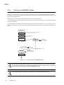
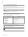
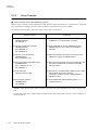
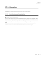
About This Manual
■Organization
In this LSI manual, this LSI functions are presented in the following order : overview, basic CPU
functions, interrupt functions, port functions, timer functions, serial functions, and other peripheral
hardware functions. Each section contains overview of function, block diagram, control register,
operation, and setting example.
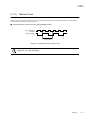
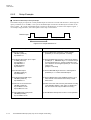
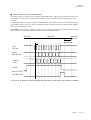
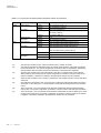
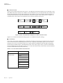
■Manual Configuration
Each section of this manual consists of a title, summary, main text, key information, precautions and
warnings, and references.The layout and definition of each section are shown below.
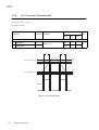
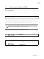
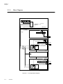
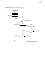
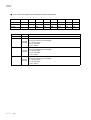
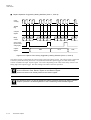
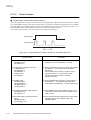
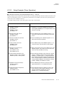
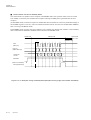
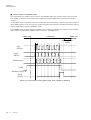
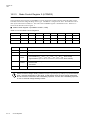
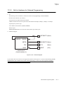
Header
Chapter number and
Chapter title
Section title
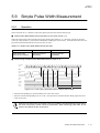
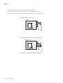
chapter 2
Basic CPU
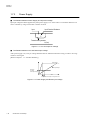
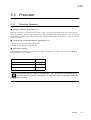
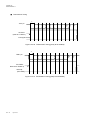
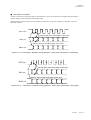
2.8 Reset
Sub section title
2.8.1
Main text
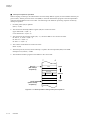
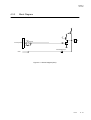
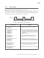
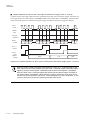
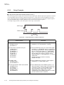
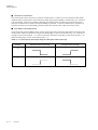
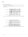
Reset operation
the CPU contents are reset and registers are intialized when the NRST pin (P
27) is pulled to low.
Initiating a Reset
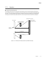
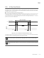
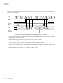
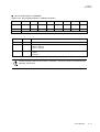
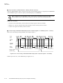
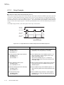
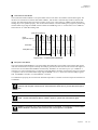
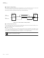
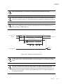
There are two methods to initiate areset.
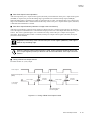
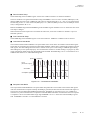
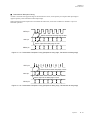
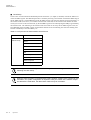
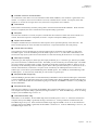
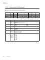
(1) Drive the NRST pin low for at least four clock cycles.
NTST pin should be holded "low" for more than 4 clock cycles (200 ns a
t a 20 NHz)
NRST pin
4 clock cycles
(200 ns at a 20 MHz)
Figure:2.8.1 MInimum Reset PUlse Width
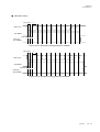
(2 Setting the P2OUT7 flag of the P2OUT register to "0" outputs low level at P
27 (NRST) pin. And transfering to reset by program (software reset) can be
executed. If the internal LSI is reset and register is initiated, the P2OUT
7 flag becomes "1" and reset is released.
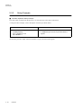
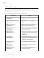
Key information
Important information
from the text.
On this LSI, the starting mode is NORMAL mode that high oscillation i
s the base clock.
When the power voltage low circuit is connected to NTST pin, circuit t
hat gives pulse for enough low level time at sudeen unconnected. And r
set can be generated even if its pulse is low level as the oscillation
clock is under 4 clocks,take notice of noise.
footer
Page # and
section title.
II-48
<About This Manual - 1>
Reset
Precautions and
warnings
Precautions are listed
in case.
Be sure to read these
of lost functionality
or damage.
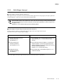
■Finding Desired Information
This manual provides three methods for finding desired information quickly and easily.
1.Consult the index at the front of the manual to locate the beginning of each section.
2.Consult the table of contents at the front of the manual to locate desired titles.
3.A chapter number and its chapter title are located at the top corner of each page, and section titles are
located at the bottom corner of each page.
■Related Manuals
Note that the following related documents are available.
• "MN101C Series LSI user's Manual"
<Describes the device hardware>
• "MN101C Series Instruction Manual"
<Describes the instruction set.>
• " Series C Compiler User's Manual: Usage Guide"
<Describes the installation, the commands, and options of the C Compiler.>
• "MN101C Series C Compiler User's Manual: Language Description"
<Describes the syntax of the C Compiler.>
• "MN101C Series C Compiler User's Manual: Library Reference"
<Describes the standard library of the C Compiler.>
• "MN101C Series Cross-assembler User's Manual"
<Describes the assembler syntax and notation.>
• "MN101C Series C Source Code Debugger User's Manual"
<Describes the use of C source code debugger.>
• About This Manual "MN101C Series PanaX Series Installation Manual"
<Describes the installation of C compiler, cross-assembler and C source code debugger and the
procedure for bringing up the in-circuit emulator.>
<About This Manual - 2>
<About This Manual - 3>
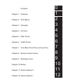
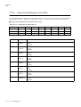
Chapter Table
Contents
Chapter 1 Overview
Chapter 2 CPU Basics
Chapter 3 Interrupts
Chapter 4 I/O Ports
Chapter 5 8-Bit Timers
Chapter 6 16-Bit Timers
Chapter 7 Time Base Timer/Free-running Timer
Chapter 8 Remote Control Career
Chapter 9 Watchdog Timer
Chapter 10 Buzzer
Chapter 11 Serial Interface 0
Chapter 12 Serial Interface 1
0
1
2
3
4
5
6
7
8
9
10
11
12
Chapter 13 Serial Interface 3
Chapter 14 Serial Interface 4
Chapter 15 A/D Converter
Chapter 16 LCD
Chapter 17 Appendix
13
14
15
16
17
Contents
Contents
0
Contents
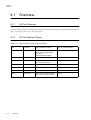
Chapter 1 Overview................................................................................................................ I-1
1.1 Overview ............................................................................................................................................. I-2
1.1.1 Overview ............................................................................................................................... I-2
1.1.2 Product Summary.................................................................................................................. I-2
1.2 Hardware Functions............................................................................................................................. I-3
1.3 Pin Description ..................................................................................................................................
1.3.1 Pin configuration .................................................................................................................
1.3.2 Pin Specification .................................................................................................................
1.3.3 Pin Functions.......................................................................................................................
I-10
I-10
I-12
I-14
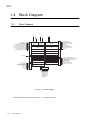
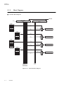
1.4 Block Diagram................................................................................................................................... I-20
1.4.1 Block Diagram .................................................................................................................... I-20
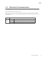
1.5 Electrical Characteristics ...................................................................................................................
1.5.1 Absolute Maximum Ratings *2,*3 ....................................................................................
1.5.2 Operating Conditions [NORMAL mode:fs=fosc/2, SLOW mode:fs=fx/2] .......................
1.5.3 DC Characteristics ..............................................................................................................
1.5.4 A/C Converter Characteristics ............................................................................................
1.5.5 A/D Converter Characteristics ............................................................................................
I-21
I-22
I-23
I-28
I-32
I-33
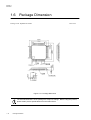
1.6 Package Dimension ........................................................................................................................... I-34
1.7 Cautions for Circuit Setup .................................................................................................................
1.7.1 General Usage .....................................................................................................................
1.7.2 Unused pins .........................................................................................................................
1.7.3 Power Supply ......................................................................................................................
1.7.4 Power Supply Circuit ..........................................................................................................
I-35
I-35
I-36
I-38
I-39
Chapter 2 CPU Basics .......................................................................................................... II-1
2.1 Overview ............................................................................................................................................ II-2
2.1.1 Block Diagram ..................................................................................................................... II-4
2.1.2 CPU Control Registers ......................................................................................................... II-6
2.1.3 Instruction Execution Controller.......................................................................................... II-7
2.1.4 Pipeline Process ................................................................................................................... II-8
2.1.5 Registers for Address ........................................................................................................... II-8
2.1.6 Registers for Data................................................................................................................. II-9
2.1.7 Processor Status Word ....................................................................................................... II-10
2.1.8 Address Space .................................................................................................................... II-12
2.1.9 Addressing Modes.............................................................................................................. II-13
2.1.10 Machine Clock ................................................................................................................. II-15
2.2 Memory Space.................................................................................................................................. II-16
<Contents - 2>
2.2.1 Memory Mode ................................................................................................................... II-16
2.2.2 Single-chip Mode............................................................................................................... II-17
2.2.3 Special Function Registers................................................................................................. II-18
2.3 Bus Interface .................................................................................................................................... II-19
2.3.1 Bus Controller.................................................................................................................... II-19
2.3.2 Control Registers ............................................................................................................... II-20
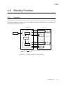
2.4 Standby Function .............................................................................................................................
2.4.1 Overview............................................................................................................................
2.4.2 CPU Mode Control Register..............................................................................................
2.4.3 Transition between SLOW and NORMAL .......................................................................
2.4.4 Transition to STANDBY Modes .......................................................................................
II-21
II-21
II-24
II-25
II-26
2.5 Clock Switching ............................................................................................................................... II-28
2.6 Reset ................................................................................................................................................. II-30
2.6.1 Reset operation .................................................................................................................. II-30
2.6.2 Oscillation Stabilization Wait time.................................................................................... II-32
Chapter 3 Interrupts ............................................................................................................. III-1
3.1 Overview ........................................................................................................................................... III-2
3.1.1 Functions............................................................................................................................. III-3
3.1.2 Block Diagram .................................................................................................................... III-4
3.1.3 Operation ............................................................................................................................ III-5
3.1.4 Interrupt Flag Setup .......................................................................................................... III-16
3.2 Control Registers............................................................................................................................. III-17
3.2.1 Registers List .................................................................................................................... III-17
3.2.2 Interrupt Control Registers ............................................................................................... III-19
3.3 External Interrupts...........................................................................................................................
3.3.1 Overview...........................................................................................................................
3.3.2 Block Diagram ..................................................................................................................
3.3.3 Control Registers ..............................................................................................................
3.3.4 Programmable Active Edge Interrupt ...............................................................................
3.3.5 Both Edges Interrupt .........................................................................................................
3.3.6 Key Input Interrupt ...........................................................................................................
3.3.7 Noise Filter .......................................................................................................................
3.3.8 AC Zero-Cross Detector ...................................................................................................
3.3.9 External Interrupt At The Standby Mode .........................................................................
III-41
III-41
III-42
III-46
III-52
III-53
III-55
III-56
III-59
III-61
Chapter 4 I/O Ports............................................................................................................... IV-1
4.1 Overview ........................................................................................................................................... IV-2
4.1.1 I/O Port Overview............................................................................................................... IV-2
4.1.2 I/O Port Status at Reset ....................................................................................................... IV-2
<Contents - 3>
4.1.3 Control Registers ................................................................................................................ IV-3
4.2 Port 1 ................................................................................................................................................. IV-5
4.2.1 Description.......................................................................................................................... IV-5
4.2.2 Registers.............................................................................................................................. IV-7
4.2.3 Block Diagram .................................................................................................................. IV-16
4.3 Port 2 ...............................................................................................................................................
4.3.1 Description........................................................................................................................
4.3.2 Registers............................................................................................................................
4.3.3 Block Diagram ..................................................................................................................
IV-22
IV-22
IV-22
IV-23
4.4 Port 3 ...............................................................................................................................................
4.4.1 Description........................................................................................................................
4.4.2 Registers............................................................................................................................
4.4.3 Block Diagram ..................................................................................................................
IV-24
IV-24
IV-26
IV-33
4.5 Port 5 ...............................................................................................................................................
4.5.1 Description........................................................................................................................
4.5.2 Registers............................................................................................................................
4.5.3 Block Diagram ..................................................................................................................
IV-39
IV-39
IV-41
IV-45
4.6 Port 7 ...............................................................................................................................................
4.6.1 Description........................................................................................................................
4.6.2 Registers............................................................................................................................
4.6.3 Block Diagram ..................................................................................................................
IV-49
IV-49
IV-51
IV-58
4.7 Port 9 ...............................................................................................................................................
4.7.1 Description........................................................................................................................
4.7.2 Registers............................................................................................................................
4.7.3 Block Diagram ..................................................................................................................
IV-66
IV-66
IV-67
IV-71
4.8 Port A ..............................................................................................................................................
4.8.1 Description........................................................................................................................
4.8.2 Registers............................................................................................................................
4.8.3 Block Diagram ..................................................................................................................
IV-72
IV-72
IV-74
IV-78
4.9 Real Time Output Control............................................................................................................... IV-82
4.9.1 Registers............................................................................................................................ IV-82
4.9.2 Operation .......................................................................................................................... IV-82
Chapter 5 8-bit Timers .......................................................................................................... V-1
5.1 Overview ............................................................................................................................................ V-2
5.1.1 Functions.............................................................................................................................. V-3
5.1.2 Block Diagram ..................................................................................................................... V-4
5.2 Control Registers................................................................................................................................ V-7
5.2.1 Registers............................................................................................................................... V-7
<Contents - 4>
5.2.2 Timer Prescaler Registers .................................................................................................... V-9
5.2.3 Programmable Timer Registers ......................................................................................... V-12
5.2.4 Timer Mode Registers ....................................................................................................... V-14
5.3 Prescaler ........................................................................................................................................... V-19
5.3.1 Prescaler Operation............................................................................................................ V-19
5.3.2 Setup Example ................................................................................................................... V-20
5.4 8-bit Timer ....................................................................................................................................... V-21
5.4.1 8-bit Timer Operation ........................................................................................................ V-21
5.4.2 Setup Example ................................................................................................................... V-24
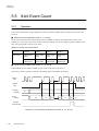
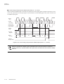
5.5 8-bit Event Count ............................................................................................................................. V-26
5.5.1 Operation ........................................................................................................................... V-26
5.5.2 Setup Example ................................................................................................................... V-29
5.6 8-bit Timer Pulse Output.................................................................................................................. V-31
5.6.1 Operation ........................................................................................................................... V-31
5.6.2 Setup Example ................................................................................................................... V-32
5.7 8-bit PWM Output............................................................................................................................
5.7.1 Operation ...........................................................................................................................
5.7.2 PWM Output with Additional Pulse..................................................................................
5.7.3 Setup Example ...................................................................................................................
V-34
V-34
V-37
V-39
5.8 Serial Transfer Clock Output ........................................................................................................... V-41
5.8.1 Operation ........................................................................................................................... V-41
5.8.2 Setup Example ................................................................................................................... V-42
5.9 Simple Pulse Width Measurement ................................................................................................... V-43
5.9.1 Operation ........................................................................................................................... V-43
5.9.2 Setup Example ................................................................................................................... V-44
5.10 Cascade Connection ....................................................................................................................... V-46
5.10.1 Operation ......................................................................................................................... V-46
5.10.2 Setup Example ................................................................................................................. V-48
Chapter 6 16-bit Timers ....................................................................................................... VI-1
6.1 Overview ........................................................................................................................................... VI-2
6.1.1 Functions............................................................................................................................. VI-2
6.1.2 Block Diagram .................................................................................................................... VI-4
6.2 Control Registers............................................................................................................................... VI-6
6.2.1 Registers.............................................................................................................................. VI-7
6.2.2 Programmable Timer Registers .......................................................................................... VI-9
6.2.3 Timer Mode Registers ...................................................................................................... VI-16
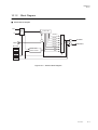
6.3 Operation......................................................................................................................................... VI-24
6.3.1 Operation .......................................................................................................................... VI-24
<Contents - 5>
6.3.2 Setup Example .................................................................................................................. VI-28
6.4 16-bit Event Count .......................................................................................................................... VI-29
6.4.1 Operation .......................................................................................................................... VI-29
6.4.2 Setup Example .................................................................................................................. VI-33
6.5 16-bit Timer Pulse Output............................................................................................................... VI-35
6.5.1 Operation .......................................................................................................................... VI-35
6.5.2 Setup Example .................................................................................................................. VI-37
6.6 16-bit Standard PWM Output (Only duty can be changed consecutively) ..................................... VI-39
6.6.1 Operation .......................................................................................................................... VI-39
6.6.2 Setup Example .................................................................................................................. VI-42
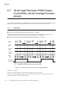
6.7 16-bit High Precision PWM Output (Cycle/Duty can be changed consecutively) ......................... VI-44
6.7.1 Operation .......................................................................................................................... VI-44
6.7.2 Setup Example .................................................................................................................. VI-47
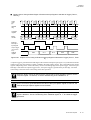
6.8 16-bit Timer Capture....................................................................................................................... VI-49
6.8.1 Operation .......................................................................................................................... VI-49
6.8.2 Setup Example .................................................................................................................. VI-55
6.9 16-bit High Precision IGBT Output (Cycle/Duty can be changed consecutively) ......................... VI-57
6.9.1 Operation .......................................................................................................................... VI-57
6.9.2 Setup Example .................................................................................................................. VI-62
6.10 16-bit Standard IGBT Output (Only duty can be changed consecutively) ................................... VI-65
6.10.1 Operation ........................................................................................................................ VI-65
6.10.2 Setup Example ................................................................................................................ VI-70
6.11 Dead Time IGBT Output .............................................................................................................. VI-72
6.11.1 Operation ........................................................................................................................ VI-72
6.11.2 Setup Example ................................................................................................................ VI-76
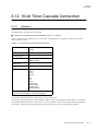
6.12 16-bit Timer Cascade Connection.................................................................................................
6.12.1 Operation ........................................................................................................................
6.12.2 Setup Example (Timer Operation)..................................................................................
6.12.3 Setup Example (PWM Operation) ..................................................................................
VI-79
VI-79
VI-81
VI-83
Chapter 7 Time Base Timer / Free-running Timer ............................................................. VII-1
7.1 Overview ......................................................................................................................................... VII-2
7.1.1 Functions........................................................................................................................... VII-2
7.1.2 Block Diagram .................................................................................................................. VII-4
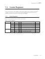
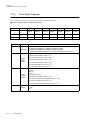
7.2 Control Registers.............................................................................................................................
7.2.1 Control Registers ..............................................................................................................
7.2.2 Programmable Timer Registers ........................................................................................
7.2.3 Timer 6 Enable Registers..................................................................................................
7.2.4 Timer Mode Registers ......................................................................................................
<Contents - 6>
VII-5
VII-5
VII-6
VII-7
VII-8
7.3 8-bit Free-running Timer................................................................................................................. VII-9
7.3.1 Operation .......................................................................................................................... VII-9
7.3.2 Setup Example ................................................................................................................ VII-13
7.4 Time Base Timer........................................................................................................................... VII-15
7.4.1 Operation ........................................................................................................................ VII-15
7.4.2 Setup Example ................................................................................................................ VII-17
Chapter 8 Remote Control Carrier Functions ................................................................... VIII-1
8.1 Overview ........................................................................................................................................ VIII-2
8.1.1 Functions.......................................................................................................................... VIII-2
8.1.2 Block Diagram ................................................................................................................. VIII-3
8.2 Control Registers............................................................................................................................ VIII-4
8.2.1 Control Registers ............................................................................................................. VIII-4
8.2.2 Remote Control Carrier Output Control Register............................................................ VIII-5
8.3 Operations ...................................................................................................................................... VIII-6
8.3.1 Operations ........................................................................................................................ VIII-6
8.3.2 Setup Examples................................................................................................................ VIII-8
Chapter 9 Watchdog Timer .................................................................................................. IX-1
9.1 Overview ........................................................................................................................................... IX-2
9.1.1 Functions............................................................................................................................. IX-2
9.1.2 Block Diagram .................................................................................................................... IX-3
9.2 Control Register ................................................................................................................................ IX-4
9.2.1 Control Registers ................................................................................................................ IX-4
9.2.2 Watchdog Timer Control Register...................................................................................... IX-4
9.3 Operation........................................................................................................................................... IX-5
9.3.1 Operation ............................................................................................................................ IX-5
9.3.2 Setup Example .................................................................................................................... IX-7
Chapter 10 Buzzer................................................................................................................. X-1
10.1 Overview .......................................................................................................................................... X-2
10.1.1 Functions............................................................................................................................ X-2
10.1.2 Block Diagram ................................................................................................................... X-3
10.2 Control Register ............................................................................................................................... X-4
10.2.1 Registers............................................................................................................................. X-4
10.2.2 Oscillation Stabilization Wait Time Control Register (DLYCTR) ................................... X-5
10.3 Operation.......................................................................................................................................... X-6
<Contents - 7>
10.3.1 Operation ........................................................................................................................... X-6
10.3.2 Setup Example ................................................................................................................... X-7
Chapter 11 Serial interface 0................................................................................................ XI-1
11.1 Overview ......................................................................................................................................... XI-2
11.1.1 Functions........................................................................................................................... XI-2
11.1.2 Block Diagram .................................................................................................................. XI-4
11.2 Control Registers.............................................................................................................................
11.2.1 Registers............................................................................................................................
11.2.2 Data Buffer Registers........................................................................................................
11.2.3 Mode Registers .................................................................................................................
11.3 Operation.......................................................................................................................................
11.3.1 Clock Synchronous Serial Interface ...............................................................................
11.3.2 Setup Example ................................................................................................................
11.3.3 UART Serial Interface ....................................................................................................
11.3.4 Setup Example ................................................................................................................
XI-5
XI-5
XI-6
XI-7
XI-13
XI-13
XI-34
XI-43
XI-60
Chapter 12 Serial interface 1............................................................................................... XII-1
12.1 Overview ....................................................................................................................................... XII-2
12.1.1 Functions......................................................................................................................... XII-2
12.1.2 Block Diagram ................................................................................................................ XII-4
12.2 Control Registers...........................................................................................................................
12.2.1 Registers..........................................................................................................................
12.2.2 Data Buffer Registers......................................................................................................
12.2.3 Mode Registers ...............................................................................................................
12.3 Operation.....................................................................................................................................
12.3.1 Clock Synchronous Serial Interface .............................................................................
12.3.2 Setup Example ..............................................................................................................
12.3.3 UART Serial Interface ..................................................................................................
12.3.4 Setup Example ..............................................................................................................
XII-5
XII-5
XII-6
XII-7
XII-13
XII-13
XII-33
XII-42
XII-59
Chapter 13 Serial Interface 3............................................................................................ XIII-1
13.1 Overview ...................................................................................................................................... XIII-2
13.1.1 Functions........................................................................................................................ XIII-2
13.1.2 Block Diagram ............................................................................................................... XIII-3
13.2 Control Registers..........................................................................................................................
13.2.1 Registers List .................................................................................................................
13.2.2 Data Buffer Register ......................................................................................................
13.2.3 Data Register..................................................................................................................
<Contents - 8>
XIII-4
XIII-4
XIII-5
XIII-5
13.2.4 Serial interface 3 Mode Register ................................................................................... XIII-6
13.3 Operation....................................................................................................................................
13.3.1 Clock Synchronous Serial Interface ............................................................................
13.3.2 Setup Example .............................................................................................................
13.3.3 Single Master IIC Serial Interface ...............................................................................
13.3.4 Setup Example .............................................................................................................
XIII-11
XIII-11
XIII-28
XIII-37
XIII-46
Chapter 14 Serial Interface 4............................................................................................ XIV-1
14.1 Overview ......................................................................................................................................
14.1.1 Functions........................................................................................................................
14.1.2 Block Diagram ...............................................................................................................
14.1.3 Control Registers ...........................................................................................................
14.1.4 Data Buffer Register ......................................................................................................
14.1.5 Mode Register................................................................................................................
XIV-2
XIV-2
XIV-3
XIV-4
XIV-5
XIV-6
14.2 Operation...................................................................................................................................... XIV-9
14.2.1 Setup Example of the Slave IIC Serial Interface ......................................................... XIV-11
Chapter 15 A/D Converter ................................................................................................. XV-1
15.1 Overview ....................................................................................................................................... XV-2
15.1.1 Functions......................................................................................................................... XV-2
15.1.2 Block Diagram ................................................................................................................ XV-3
15.2 Control Registers...........................................................................................................................
15.2.1 Registers..........................................................................................................................
15.2.2 Control Registers ............................................................................................................
15.2.3 Data Buffers ....................................................................................................................
XV-4
XV-4
XV-5
XV-7
15.3 Operation....................................................................................................................................... XV-8
15.3.1 Setup ............................................................................................................................. XV-10
15.3.2 Setup Example .............................................................................................................. XV-12
15.3.3 Cautions ........................................................................................................................ XV-14
Chapter 16 LCD ................................................................................................................ XVI-1
16.1 Functions ......................................................................................................................................
16.1.1 Functions........................................................................................................................
16.1.2 LCD Operation in Standby Mode ..................................................................................
16.1.3 Maximum Pixels ............................................................................................................
16.1.4 Switching I/O ports and LCD segment pins ..................................................................
16.1.5 Switching I/O Ports and LCD Voltage¶ ........................................................................
16.1.6 Block Diagram ...............................................................................................................
XVI-2
XVI-2
XVI-3
XVI-4
XVI-4
XVI-4
XVI-5
16.2 Control Registers.......................................................................................................................... XVI-6
<Contents - 9>
16.2.1 Registers......................................................................................................................... XVI-6
16.2.2 Mode Control Register 1 (LCDMD1) ........................................................................... XVI-7
16.2.3 Mode Control Register 2 (LCDMD2) ........................................................................... XVI-8
16.2.4 Output Control Register 1 (LCCTR1) ........................................................................... XVI-9
16.2.5 Output Control Register 2 (LCCTR2) ......................................................................... XVI-10
16.2.6 Output Control Register 3 (LCCTR3) ......................................................................... XVI-11
16.2.7 Segment Output Latch ................................................................................................. XVI-12
16.3 Operation....................................................................................................................................
16.3.1 Operation .....................................................................................................................
16.3.2 Power Supply ...............................................................................................................
16.3.3 Frame Cycle .................................................................................................................
16.3.4 Setup Example of the LCD Driver Circuit ..................................................................
XVI-13
XVI-13
XVI-14
XVI-19
XVI-20
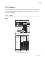
16.4 Display .......................................................................................................................................
16.4.1 Static ............................................................................................................................
16.4.2 Setup Example (Static) ................................................................................................
16.4.3 1/2duty .........................................................................................................................
16.4.4 Setup Example (1/2 duty) ............................................................................................
16.4.5 1/3 duty ........................................................................................................................
16.4.6 Setup Example (1/3 duty) ............................................................................................
16.4.7 1/4 duty ........................................................................................................................
16.4.8 Setup Example (1/4 duty) ............................................................................................
XVI-21
XVI-21
XVI-23
XVI-24
XVI-26
XVI-27
XVI-29
XVI-30
XVI-32
Chapter 17 Appendix ....................................................................................................... XVII-1
17.1 Flash EEPROM ........................................................................................................................... XVII-2
17.1.1 Overview....................................................................................................................... XVII-2
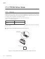
17.2 PROM Writer Mode.................................................................................................................... XVII-4
17.2.1 Overview....................................................................................................................... XVII-4
17.3 Onboard Serial Programming Mode ........................................................................................... XVII-5
17.3.1 Overview....................................................................................................................... XVII-5
17.3.2 Circuit Requirements for the Target Board .................................................................. XVII-6
17.3.3 Built-in Hardware for Onboard Programming.............................................................. XVII-7
17.3.4 MN101CF78A Clock on the Target Board................................................................... XVII-8
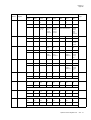
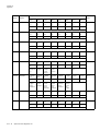
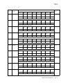
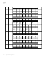
17.4 Special Function Registers List................................................................................................... XVII-9
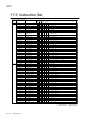
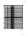
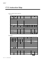
17.5 Instruction Set ........................................................................................................................... XVII-28
17.6 Instruction Map ......................................................................................................................... XVII-34
<Contents - 10>
I..
Chapter 1 Overview
1
Chapter 1
Overview
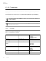
1.1 Overview
1.1.1
Overview
The MN101C series of 8-bit single-chip microcomputers incorporate multiple types of peripheral functions. This
chip series is well suited for camera, VCR, MD, TV, CD, LD, printer, telephone, home automation, pager, air conditioner, PPC, remote control, fax machine, music instrument and other applications.
This LSI brings to embedded microcomputer applications flexible, optimized hardware configurations and a simple efficient instruction set. The MN101C78A has an internal 32 KB of ROM and 1.5 KB of RAM. Peripheral
functions include 4 external interrupts, 18 internal interrupts including NMI, 9 timer counters, 4 sets of serial
interfaces, A/D converter, watchdog timer, buzzer output, and remote control output. The configuration of this
microcomputer is well suited for application as a system controller in a camera, timer selector for VCR, CD
player, or MD.
With two oscillation system (max. 10 MHz/32 kHz) contained on the chip, the system clock can be switched to
high frequency input (high speed mode), or to low frequency input (low speed mode).
The system clock is generated by dividing the oscillation clock. The best operation clock for the system can be
selected by switching its frequency by software. High speed mode has the normal mode which is based on 2cycle clock (fosc/2) and the double speed mode which is based on the same cycle clock with fosc.
A machine cycle (min. instructions execution) in the normal mode is 250 ns when fosc is 8 MHz, and when fosc
is 10 MHz, a machine cycle is 200 ns. A machine cycle in the double speed mode is 125 ns when fosc is 8 MHz,
and 100 ns when fosc is 10 MHz. Two types of packages are available, 48-pin TQFP and 44-pin QFP.
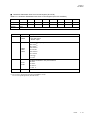
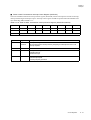
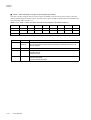
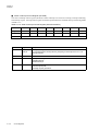
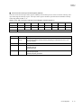
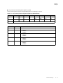
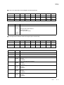
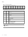
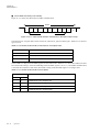
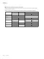
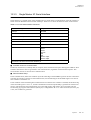
1.1.2
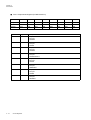
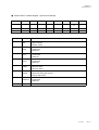
Product Summary
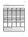
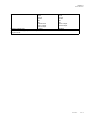
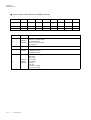
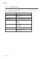
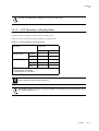
This manual describes the following models of the MN101C78 series. These products have identical functions.
However, MN101C78A is described mainly.
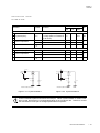
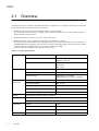
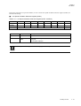
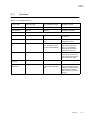
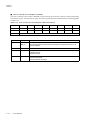
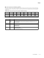
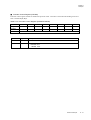
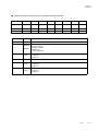
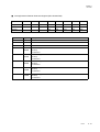
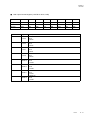
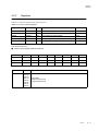
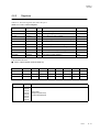
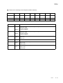
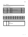
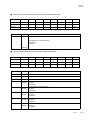
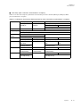
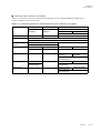
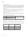
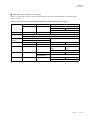
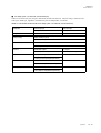
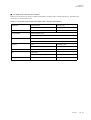
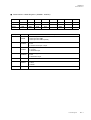
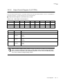
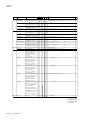
Table:1.1.1 Product Summary
I-2
Model
ROM Size
RAM Size
Classification
MN101C78A*1
32 KB
1.5 KB
Mask ROM version
MN101C789*2
24 KB
1.5 KB
Mask ROM version
MN101CF78A*1
32 KB
1.5 KB
Flash EEPROM version
Overview
*1
Under development
*2
Under consideration
Chapter 1
Overview
1.2 Hardware Functions
■ Functions
- ROM capacity:
32768x8 bit *1
- RAM capacity:
1536x8 bit *1
*1 Differs depending upon the model. Refer to [Chapter 1 1-1-2 Product Summary]
- Package:
QFP44 (10 mm square, 0.8 mm pitch)
TQFP48 (7 mm square, 0.5 mm pitch)
- Machine cycle:
High speed mode <fs=fosc/2, fosc/1>
0.125 ms / -, 8 MHz (2.7 V to 3.6 V)
0.25 ms / 8 MHz, 4 MHz (2.3 V to 3.6 V) *2
0.50 ms / 4 MHz, 2 MHz (1.8 V to 3.6 V) *2
Low speed mode <fs=fx / 2>
62.5 ms / 32 kHz (1.8 V to 3.6 V) *2
*2 The guaranteed operating range for Flash EEPROM version MN1010CF78A is 2.7 V to 3.6 V.
- Internal clock gear:
Operation speed of internal system clock is variable by changing the frequency.
(2, 4, 16, 32, 64, 128 dividing)
- Oscillating circuit:
Two oscillation circuits (high speed / low speed)
- Operation modes:
NORMAL mode
SLOW mode
HALT mode
STOP mode
(The operation clock can be switched in each model)
- Operating voltage:
1.8 V to 3.6 V (Flash version of TQFP48, MN101CF78A is 2.7 V to 3.6 V)
- Operating temperature:
-40 C to +85 C
- Interrupt:
22 levels
<External interrupts>
Edge selectable.
IRQ0: External interrupt (AC zero cross detector. With/Without noise filter)
IRQ1: External interrupt (AC zero cross detector. With/Without noise filter)
IRQ2: External interrupt (Both edges selectable IRQ3 – external interrupt)
IRQ3: (Key scan interrupt only)
Hardware Functions
I-3
Chapter 1
Overview
<Timer interrupts>
TM0IRQ: Timer 0 interrupt (8-bit timer)
TM1IRQ: Timer 1 interrupt (8-bit timer)
TM2IRQ: Timer 2 interrupt (8-bit timer)
TM3IRQ: Timer 3 interrupt (8-bit timer)
TM7IRQ: Timer 7 interrupt (16-bit timer)
T7OC2IRQ: Timer 7 compare register 2 interrupt (16-bit timer)
TM8IRQ: Timer 8 interrupt (16-bit timer)
T8OC2IRQ: Timer 8 compare register 2 interrupt (16-bit timer)
TM6IRQ: Timer 6 interrupt (8-bit timer)
TBIRQ: Time base timer interrupt
<Serial interface interrupts>
SC0RIRQ: Serial interface 0 interrupt (UART reception)
SC0TIRQ: Serial interface 0 interrupt (UART transmission, synchronous)
SC1RIRQ: Serial interface 1 interrupt (UART reception)
SC1TIRQ: Serial interface 1 interrupt (UART transmission, synchronous)
<Watchdog timer interrupt>
SC3IRQ:
Serial interface 3 interrupt (Single master IIC, synchronous)
SC4IRQ:
Serial interface 4 interrupt (Slave IIC)
NMI: Non-maskable interrupt
<A/D conversion end interrupt> ADIRQ: A/D conversion interrupt
- A/D converter:
10-bit x 7 channels
- Timer counter:
9 timers All timer counters generate interrupt
Timer 0 (8-bit timer for general use)
Square wave output, PWM output, Event count, Simple pulse width measurement,
Clock source: fosc, fosc/4, fosc/16, fosc/32, fosc/64, fs/2, fs/4, fx, external clock
P50 of the large current pin (TM0OA) or P15 (TM0OB) for PWM output
Timer 1 (8-bit timer for general use or UART baud rate timer)
Square wave output, Event count, Cascade connection to timer 0
Clock source: fosc, fosc/4, fosc/16, fosc/64, fosc/128, fs/2, fs/8, fx, external clock
Timer 2 (8-bit timer for general use or UART baud rate timer)
Square wave output, PWM output, Event count, Simple pulse width measurement
Clock source: fosc, fosc/4, fosc/16, fosc/32, fosc/64, fs/2, fs/4, fx, external clock
Added pulse (2-bit) system PWM
P52 of the large current pin (TM2OA) or P16 (TM2OB) for PWM output
I-4
Hardware Functions
Chapter 1
Overview
Timer 3 (8-bit timer for general use)
Square wave output, Event count,
Cascade connection to timer2
Clock source: fosc, fosc/4, fosc/16, fosc/64, fosc/128, fs/2, fs/8, fx, external clock
Timer 6 (8-bit timer for general use)
Combined with time base timer, it can be set to measure one minute intervals.
12
13
Clock source: fosc, fs, fx, time base output (1/2 or 1/2 )
Timer 7 (16-bit timer for general use)
Square wave output, P51 of the large-current pin (TM7O) for PWM output and IGBT control output
(Duty/Cycle continuous variable), Event count, Pulse width measurement, Input capture, Cascade
connection to timer 8 (32-bit timer, 32-bit PWM, input capture can be used)
Clock source: 1/1, 1/2, 1/4, 1/16 of any one of fosc, fx, or external clock
Timer 8 (16-bit timer double buffering)
Square wave output, P53 of the large-current pin (TM8O) for PWM output (Duty continuous variable),
Event count, pulse width measurement, Input capture
Time base timer
Clock source: fosc, fx
7
8
9
10
13
15
Interrupt enable for source clock at the dividing output of 1/2 , 1/2 , 1/2 , 1.2 , 1/2 , 1/2
Watchdog timer
16
18
Watchdog timer frequency can be selected from fs/2 , fs/2 , fs/2
20
- Buzzer output, Inverted buzzer output:
9
10
11
13
14
3
4
Output frequency can be selected from fosc/2 , fosc/2 , fosc/2 , fosc/2 , fosc/2 , fx/2 , fx/2 .
- Remote control carrier output:
Based on the timer 0 and timer 3 output, a remote control carrier with duty cycle of 1/2 or 1/3 can be
output.
- Clock output:
OSC oscillation source or system clock output can be selected.
Clock source: 1/1, 1/2, 1/4, 1/16 of any one of fosc, fx, or external clock
Hardware Functions
I-5
Chapter 1
Overview
- Serial interface:
4 types
Serial interface 0, 1: 2 channels
CH0: Duplex UART / Synchronous serial interface
- Transfer clock: focs/2, focs/4, focs/16, focs/64, fs/2, fs/4, 1/2 of timer 1 (timer 2) output
- Timer 1 (or timer2) is used as baud rate timer at UART.
- MSB/LSB can be selected as the first bit to be transferred. An arbitrate transfer size from 1 to 8
bits can be selected.
- It can be used as parity check, overrun error, framing error detection, or 2 channels serial
interface.
CH1: Duplex UART / Synchronous serial interface
- Transfer clock: focs/2, focs/4, focs/16, focs/64, fs/2, fs/4, 1/2 of timer 1 (timer 2) output
- Timer 1 (or timer2) is used as baud rate timer at UART.
- MSB/LSB can be selected as the first bit to be transferred. An arbitrate transfer size from 1 to 8
bits can be selected.
- It can be used as parity check, overrun error, framing error detection, or 2 channels serial
interface.
Serial interface 1 I/O (SBO1, SBI1, SBT1) can be switched to P15 to P17 or PA5 to PA7. (48
pin version only)
Serial interface 0 I/O (SBO0, SBI0, SBT0) can be switched to P75 to P77 or PA0 to PA2. (44
pin version/ 48 version)
Serial interface 3: 1 channel
Single master IIC / Synchronous serial interface
- Single master handling IIC communication enable (with ACK, 9 bits are transferred)
- Transfer clock: focs/2, focs/4, focs/16, focs/32, focs/64, fs/2, fs/4, timer 2 (timer 3) output
- MSB/LSB can be selected as the first bit to be transferred. An arbitrate transfer size from 1 to 8
bits can be selected.
Serial interface 4: 1 channel
IIC slave interface
- IIC high-speed transfer mode (communication speed: 400 kbps)
- 7-bit or 10-bit of slave address can be set.
- General call communication mode handling
(SCL pin, SDA pin can be switched to P10, P11, or P76, P77)
I-6
Hardware Functions
Chapter 1
Overview
- LED driver:
4 pins
LCD driver pins:
Segment output 12 pins max. (SEG0 to SEG11)
SEG0 to SEG11 are switchable to I/O ports in unit of 1 pin.
[Note: At reset, SEG0 to SEG11 are input pors.]
Common output pins: 4 pins
COM0 to COM3 are switchable to I/O port in 1 pin unit.
Display mode selection
Static
1/2 duty, 1/2 bias
1/3 duty, 1/3 bias
1/4 duty, 1/4 bias
LCD driver clock
The source clock is the main clock (fosc):
18
17
16
15
14
13
12
11
1/2 , 1/2 , 1/2 , 1/2 , 1/2 , 1/2 , 1/2 , 1/2
The source clock is the sub-clock (fx)
9
8
7
6
1/2 , 1/2 , 1/2 , 1/2
LCD power supply
Available at VDD>VLC1
External supply voltage is supplied by VLC1, VLC2, VLC3 pins or voltage applied to VLC1 is divided
by internal resistance and supplied to VLC2 and VLC3 pins
Hardware Functions
I-7
Chapter 1
Overview
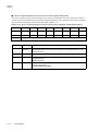
- Port:
48 pin
44 pin
version
version
39 pins
35 pins
(dual function)
(dual function)
4 pins
44 pins
LCD power supply pin
3 pins
3 pins
A/D input pin
1 pin
1 pin
A/D input/ Serial interface pin
6 pins
3 pins
Timer I/O / LCD driver/ Remote control carrier output pin
1 pin
1 pin
Timer output/ LCD driver/ Serial interface pin
2 pins
2 pins
Timer I/O /LCD driver/ Serial interface pin
1 pin
1 pin
Timer I/O /Buzzer output/ LCD driver pin
1 pin
1 pin
Timer I/O /inverted buzzer output/ LCD driver pin
1 pin
1 pin
IIC slave pin
2 pins
2 pins
Key input/ LCD driver pin
3
3
Key input/ LCD driver/ PWM output pin
2
2
Key input/ LCD driver/ Serial interface pin
1
1
Key input/ LCD driver/ Serial interface/ IIC slave pin
2
2
Common output pin
1
1
Common output/ Serial interface pin
3
3
External interrupt pin
3
3
I/O ports
1
-
XI pin
1
1
Special pin
10
10
Analog reference voltage input pin
1
1
Operation mode input pin
1
1
Reset input pin
1
1
Oscillation pin (1 pin is used as I/O pin)
4
4
Power supply pin
3
3
I/O ports
LED (large current) driver pin
(switchable to timer output)
(2 pins are used as zero cross input pin)
I-8
Hardware Functions
Chapter 1
Overview
- Pin switching:
Serial interface I/O
Option 1
Option 2
Option 3
Serial interface 0
SBT0A
SBT0B
-
Synchronous/ UART
SBO0A/TXD0A
SBO0B/TXD0B
STI0A/RXD0A
STI0B/RXD0B
*UART for onboard serial
programming
Serial interface 1
SBT1A
SBT1B
Synchronous/ UART
SBO1A/TXD1A
SBO1B/TXD1B
STI1A/RXD1A
STI1B/RXD1B
-
*44 pin version is not
available
-
-
SDA4A
SDA4B
-
SCL4A
SCL4B
Serial interface 3
SBT3
Synchronous/ IIC single
SBT03
master
SBI3
Serial interface 4
IIC slave
*D-Wire for onboard serial
programming
Timer I/O
Option 1 (I/O)
Option 2 (output 1)
Option 3 (output 2)
Timer 0
TM0IO
TM0OA
TM0OB
Timer 1
TM1IO
-
-
Timer 2
TM2IO
TM2OA
TM2OB
Timer 3
TM3IO
-
-
Timer 7
TM7IO
TM7O
-
Timer 8
TM8IO
TM8O
-
Hardware Functions
I-9
Chapter 1
Overview
1.3 Pin Description
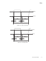
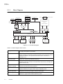
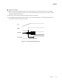
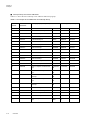
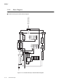
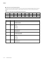
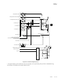
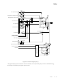
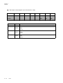
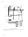
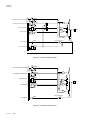
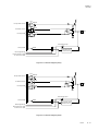
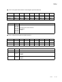
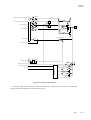
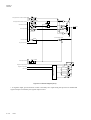
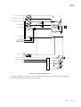
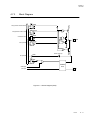
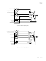
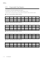
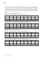
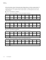
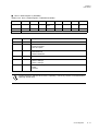
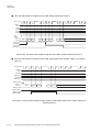
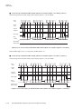
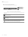
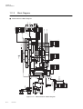
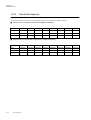
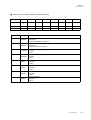
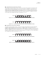
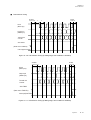
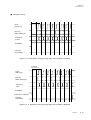
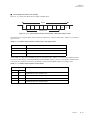
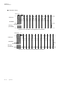
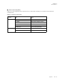
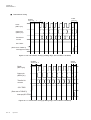
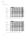
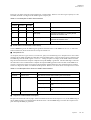
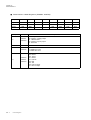
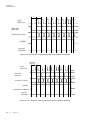
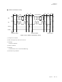
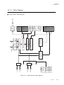
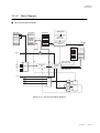
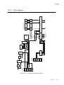
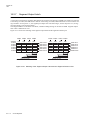
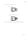
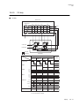
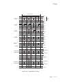
Pin configuration
P54/IRQ0/ACZ0
22
SBT1B/PA6/AN6
21
TXD1B/SBO1B/PA5/AN5
10
11
12
XI/P90
VDD
VSS
XO
P10/SDA4A
MMOD
NRST,P27
P11/SCL4A
13
7
8
9
Vref+
14
6
TXD0A/SBO0A/PA0/AN0
15
OSC1
RXD0A/SBI0A/PA1/AN1
16
OSC2
SBT0A/PA2/AN2
17
4
5
18
3
48 pin LCD version
TM8O/LED3/P53
PA3/AN3
2
RXD1B/SBI1B/PA4/AN4
19
Figure:1.3.1 Pin Configuration (48TQFP: TOP VIEW)
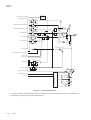
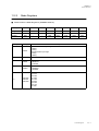
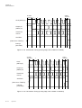
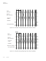
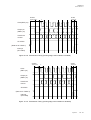
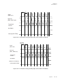
I - 10
Pin Description
VDD
MN101C78A
TM7O/LED1/P51
TM0OA/LED0/P50
24
23
20
TM2OA/LED2/P52
37
38
39
40
41
42
43
44
45
46
47
48
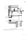
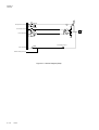
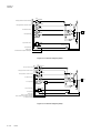
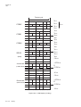
1
SEG3/P74/KEY4
SEG2/P75/KEY5/TXD0B/SBO0B
SEG1/P76/KEY6/RXD0B/SBI0B/SDA4B
SEG0/P77/KEY7/SBT0B/SCL4B
COM0/P30
COM1/P31/SBI3
COM2/P32/SBT3/SCL3
COM3/P33/SB03/SDA3
P34/VLC3
P35/VLC2
P36/VLC1
P37
34
33
32
31
30
29
28
27
26
25
36
35
SEG4/P73/KEY3
SEG5/P72/KEY2
SEG6/P71/KEY1/TM3IO
SEG7/P70/KEY0/TM1IO
SEG8/P17/SBT1A/TM2OB
SEG9/P16/TM2IO/RXD1A/SBI1A
SEG10/P15/TM0OB/TXD1A/SBO1A
SEG11/P14/TM0IO/RMOUT
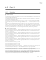
NBUZZER/P13/TM7IO/CLKOUT
BUZZER/P12/TM8IO
P56/IRQ2
P55/IRQ1/ACZ1
1.3.1
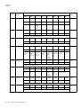
BUZZER/P12/TM8IO
P56/IRQ2
NBUZZER/P13/TM7IO/CLKOUT
SEG11/P14/TM0IO/RMOUT
SEG9/P16/TM2IO/RXD1A/SBI1A
SEG10/P15/TM0OB/TXD1A/SBO1A
27
26
25
24
23
SEG8/P17/SBT1A/TM2OB
SEG7/P70/KEY0/TM1IO
SEG6/P71/KEY1/TM3IO
SEG5/P72/KEY2
33
32
31
30
29
28
SEG4/P73/KEY3
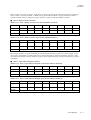
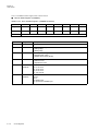
Chapter 1
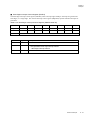
Overview
SEG3/P74/KEY4
SEG2/P75/KEY5/TXD0B/SBO0B
34
22
P55/IRQ1/ACZ1
35
21
P54/IRQ0/ACZ0
SEG1/P76/KEY6/RXD0B/SBI0B/SDA4B
36
20
VDD
SEG0/P77/KEY7/SBT0B/SCL4B
37
19
PA3/AN3
COM0/P30
38
18
SBT0A/PA2/AN2
COM1/P31/SBI3
39
17
RXD0A/SBI0A/PA1/AN1
COM2/P32/SBT3/SCL3
40
16
TXD0A/SBO0A/PA0/AN0
COM3/P33/SB03/SDA3
41
15
Vref+
P34/VLC3
42
14
P11/SCL4A
P35/VLC2
43
13
P10/SDA4A
P36/VLC1
44
12
NRST,P27
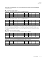
MN101C78A
4
5
6
7
8
9
10
11
TM8O/LED3/P53
OSC2
OSC1
XO
MMOD
XI/P90
3
TM2OA/LED2/P52
VDD
2
TM7O/LED1/P51
VSS
1
TM0OA/LED0/P50
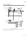
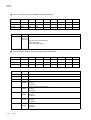
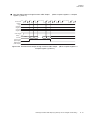
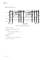
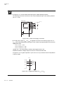
44 pin LCD version
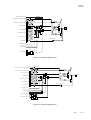
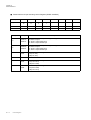
Figure:1.3.2 Pin Configuration (44QFP: TOP VIEW)
Pin Description
I - 11
Chapter 1
Overview
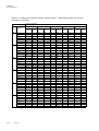
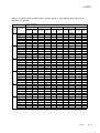
1.3.2
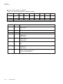
Pin Specification
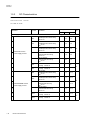
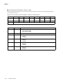
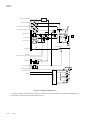
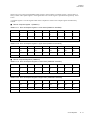
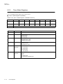
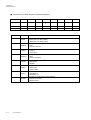
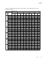
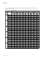
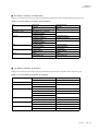
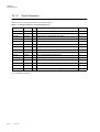
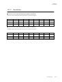
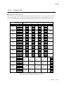
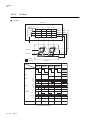
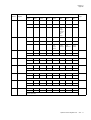
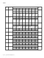
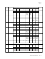
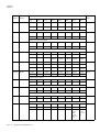
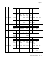
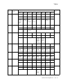
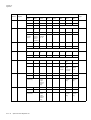
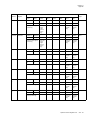
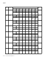
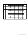
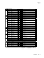
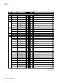
Table:1.3.1 Pin Specification
Pins
Special Functions
I/O
Direction Pin
Control
Control
P10
SDA4A
in/out
P1DIR0
P1PLU0
SDA4A: IIC4 Data I/O
P11
SCL4A
in/out
P1DIR1
P1PLU1
SCL4A: IIC4 Clock I/O
P12
TM8IO
BUZZER
in/out
P1DIR2
P1PLU2
TM8IO: Timer 8 I/O
BUZZER: Buzzer output
P13
TM7IO
NBUZZER
in/out
P1DIR3
P1PLU3
TM7IO: Timer 7 I/O
NBUZZER: Buzzer reverse output
CLKOU
T
P14
TM0IO
CLKOUT: Frequency output
RMOUT
in/out
P1DIR4
P1PLU4
SEG11
P15
P16
P17
P27
TM0IO: Timer 0 I/O
RMOUT: Remote control carrier
output
SEG11: Segment output
TM00B
SB01A
TXD1A
SEG10
TM2IO
SBI1A
in/out
in/out
RXD1A
SEG9
in/out
TM2OB
SBT1A
in/out
P1DIR5
P1PLU5
TMOOB: Timer 8 I/O
SB01A: Serial interface
transmission data output
TXD1A: UART1 transmission data
output
SEG10: Segment output
P1DIR6
P1PLU6
TM2IO: Timer 2 I/O
SBI1A: Serial interface 1 reception
data input
RXD1A: UART1 reception data input
SEG9: Segment output
P1DIR7
P1PLU7
TM2OB: Timer 2 output
SBT1A: Serial interface 1 clock I/O
SEG8
SEG8: Segment output
NRST
in
-
-
NRST: Reset
P30
COM0
in/out
P3DIR0
P3PLU0
COM0: LCD common output
P31
SBI3
COM1
in/out
P3DIR1
P3PLU1
COM1: LCD common output
SBI3: Serial interface 3 reception
data input
P32
SBT3
SCL3
in/out
P3DIR2
P3PLU2
COM2: LCD common output
SBT3: Serial interface 3 clock I/O
COM2
P33
SBO3
SCL3: IIC3 clock output
SDA3
in/out
P3DIR3
P3PLU3
COM3
P34
COM3: LCD common output
SBO3: Serial interface 3
transmission data output
SDA3: Serial data I/O
VLC3
in/out
VLC3: LCD power
P35
VLC2
in/out
P36
VLC1
in/out
-
-
in/out
P3DIR7
P3PLU7
P37 *1
VLC2: LCD power
VLC1: LCD power
P50
TM0OA
LED0
in/out
P5DIR0
P5PLU0
TM0OA: Timer 0 output
P51
TM7O
LED1
in/out
P5DIR1
P5PLU1
TM70: Timer 7 output
LED1: LED driver pin 1
P52
TM2OA
LED2t
in/out
P5DIR2
P5PLU2
TM2OA: Timer 2 output
LED2: LED driver pin 2
P53
TM8O
LED3
in/out
P5DIR3
P5PLU3
TM8O: Timer 8 output
LED3: LED driver pin 3
P54
IRQ0
ACZ0
in/out
P5DIR4
P5PLU4
IRQ0: External interrupt 0
ACZ0: Zero cross input 0
P55
IRQ1
ACZ1
in/out
P5DIR5
P5PLU5
IRQ1: External interrupt 1
ACZ1: Zero cross input 1
P56
IRQ2
in/out
P5DIR6
P5PLU6
IRQ2: External interrupt 2
P70
TM1IO
KEY0
in/out
P7DIR0
P7PLU0
TM1IO: Timer 1 I/O
P71
TM3IO
KEY1
in/out
P7DIR1
P7PLU1
TM3IO: Timer 1 I/O
SEG7
LED0: LED driver pin 0
KEYO: Key interrupt input 0
SEG7: Segment output
SEG6
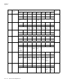
I - 12
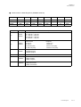
Functions Description
KEY1: Key interrupt input 1
SEG6: Segment output
P72
KEY2
SEG5
in/out
P7DIR2
P7PLU2
KEY2: Key interrupt input 2
SEG5: Segment output
P73
KEY3
SEG4
in/out
P7DIR3
P7PLU3
KEY3: Key interrupt input 3
SEG4: Segment output
P74
KEY4
SEG3
in/out
P7DIR4
P7PLU4
KEY4: Key interrupt input 4
SEG3: Segment output
Pin Description
Chapter 1
Overview
Pins
Special Functions
I/O
Direction Pin
Control
Control
Functions Description
P75
SBO0B
in/out
P7DIR5
P7PLU5
SBO0B: Serial interface 0
transmission data output
TXD0B: UART0 transmission data
output
KEY5: Key interrupt input 5
SEG2: Segment output
in/out
P7DIR6
P7PLU6
SBI0B: Serial interface 0 reception
data input
RXD0B: UART0 reception data
input
SDA4B:IIC4 data I/O
KEY6: KEY interrupt input 6
P76
TXD0B
KEY5
SEG2
SBIOB
RXDOB
SDA4B
KEY6
SEG1
P77
SEG1: Segment output
SBT0B
SCL4B
KEY7
SEG0
P90
XI
PA0
SBO0A
PA1
SBI0A
PA2
SBT0A
PA3
PA4
*1
in/out
P7DIR7
P7PLU7
SEG0: Segment 0 output
P9DIR0
P9PLU0
XI: Low speed frequency input pin
TXD0A
in/out
PADIR0
PAPLU0
SBO0A: Serial interface 0 data output TXD0A: UART0 transmission data
output
RXD0A
in/out
PADIR1
PAPLU1
SBI0A: Serial interface 0 data input
AN2
in/out
PADIR2
PAPLU2
SBT0A: Serial interface 0 clock I/O
AN3
in/out
PADIR3
PAPLU3
AN3: Analog 3 input
AN4
in/out
PADIR4
PAPLU4
AN4: Analog 4 input
AN0: Analog 0 input
AN1
SBI1B
RXD1B
SBO1B
TXD1B
in/out
PADIR5
AN6
in/out
PADIR6
SBT1B
RXD0A: UART0 reception data
input
AN1: Analog 1 input
AN2: Analog 2 input
SBI1B: Serial interface 1 data input
RXD1B: UART1 reception data
input
PAPLU5
SBO1B: Serial interface 1
transmission data output
TXD1B: UART1 transmission data
output
PAPLU6
SBT1B: Serial interface 1 clock I/O
AN5
PA6
*1
SCL4B: IIC4 clock I/O
KEY7: Key interrupt input 7
in
AN0
PA5
*1
SBT0B: Serial interface 0 clock I/O
AN5: Analog 5 input
AN6: Analog 6 input
* 1 Not available for 44 pin QFP package
Pin Description
I - 13
Chapter 1
Overview
1.3.3
Pin Functions
Table:1.3.2 Pin Functions
I - 14
Name
TQFP 48
Pin No.
QFP44
Pin No.
VSS
VDD
Vref +
5
8, 23
15
5
8, 20
15
-
Power supply pins Supply 1.8 V to 3.6 V to VDD and 0 V to VSS.
For MN101CF78A, supply 2.7 V to 3.6 V to
VDD
OSC1
OSC2
7
6
7
6
Input
Output
Clock input pins
Clock output pins
Connect these oscillation pins to ceramic or
crystal ocsillators for high-frequency clock
operation.
If the clock is an external input, connect it to
OSC1 and leave OSC2 open. The chip will
not operate with an external clock when
using either the STOP or SLOW modes.
XI
XO
9
10
9
10
Input
Output
P90
Clock input pins
Clock output pins
Connect these oscillation pins to crystal
oscillators for low-frequency clock operation.
If the clock is an external input, connect it to
XI and leave XO open. When using the
STOP mode, the chip will not operate with an
external clock. If these pins are not used,
connect XI to VSS and leave XO open.
NRST
12
12
Input
P27
Reset pins
[Active low]
This pin resets the chip when power is turned
on, is allocated as P27 and contains an
internal pull-up resistor (Type. 35 kw).
Setting this pin “L” level initialize the internal
state of the device.
Thereafter, setting the input to “H” level
releases the reset. The hardware waits for
the system clock to stabilize, then processes
the reset interrupt.
Also, if “0” is written to P27 and the reset is
initiated by software, “L” level will be output.
The output has an N-ch open-drain
configuration. If a capacitor is to be inserted
between NRST and VSS, it is recommended
that a discharge diode be placed between
NRST and VDD.
P10
P11
P12
P13
P14
P15
13
14
27
28
29
30
13
14
24
25
26
27
I/O
P16
P17
31
32
28
29
SDA4A
I/O port 0
SCL4A
TM8IO, BUZZER
TM7IO, NBUZZER, CLKOUT
TM0IO, RMOUT, SEG11
TM0OB, SBO1A, TXD1A,
SEG10
TM2IO, SBI1A, RXD1A, SEG9
TM2OB, SBI1A, SEG8
MMOD
11
11
Input
P27
12
12
Input
Pin Description
I/O
Other Function
NRST
Function
Description
8-bit COMS tri-state I/O port.
Each bit can be set individually as either an
input or output by the P1DIR register. A pullup / pull-down resistor for each bit can be
selected individually by the P1PLU register.
A pull-up / pull-down resistor for each port
can be selected individually by the SELUD
register. (However, pull-up and pull-down
resistors cannot be mixed.)
At reset, the input mode is selected and P10,
P11 are pull-up resistor enable ("H" output),
P12 to P17 are pull-up resistor disable
(output"H", "Hi-Z").
Memory mode
setting pins
Input always "L" level. It is used for Flash
programming only.
I/O port 2
Port P27 has an N-ch open-drain
configuration. When “0” is written and the
reset is initiated by software, “L” level will be
output.
Chapter 1
Overview
Name
TQFP 48
Pin No.
QFP44
Pin No.
P30
P31
P32
P33
P34
P35
P36
P37 *1
41
42
43
44
45
46
47
48
38
39
40
41
42
43
44
P50
P51
P52
P53
P54
P55
P56
1
2
3
4
24
25
26
I
2
3
4
21
22
23
P70
P71
P72
P73
P74
P75
P76
33
34
35
36
37
38
39
30
31
32
33
34
35
36
P77
40
37
P90
9
PA0
PA1
PA2
PA3
PA4 *1
PA5 *1
PA6 *1
SBO0A
SBO0B
SBO1A
SBO1B *1
SBO3
Other Function
Function
Description
COM0
SBI3, COM1
SBT3, SCL3, COM2
SBO3, SDA3, COM3
VLC3
VLC2
VLC1
I/O port 3
8-bit COMS tri-state I/O port.
Each bit can be set individually as either an
input or output by the P3DIR register. A pullup resistor for each bit can be selected
individually by the P3PLU register.
At reset, the input mode is selected and
P37is pull-up resistor enable ("H" output),
P31 to P37 are pull-up resistor disable
(output "H", "Hi-Z").
I/O
TM0OA, LED0
TM7O, LED1
TM2OA, LED2
TM8O, LED3
IRQ0, ACZ0
IRQ1, ACZ1
IRQ2
I/O port 5
7-bit COMS tri-state I/O port.
Each bit can be set individually as either an
input or output by the P5DIR register. A pullup resistor for each bit can be selected
individually by the P5PLU register.
Also, at output, LED direct drive is enabled
for P50 to P53.
At reset, the input mode is selected and pullup resistors are disabled (output “H”, “Hi-Z”).
I/O
I/O port 7
TM1IO, KEY0, SEG7
TM3IO, KEY1, SEG6
KEY2, SEG5
KEY3, SEG4
KEY4, SEG3
SBO0B, TXD0B, KEY5, SEG2
SBI0B, RXD0B, SDA4B,
KEY6, SEG1
SBT0B, SCL4B, KEY7, SEG0
8-bit COMS tri-state I/O port.
Each bit can be set individually as either an
input or output by the P7DIR register. A pullup / pull-down resistor for each bit can be
selected individually by the P7PLU register. A
pull-up / pull-down resistor for each port can
be selected individually by the SELUD
register. (However, pull-up and pull-down
resistors cannot be mixed.)
At reset, the input mode is selected and pullup resistors are disabled (output “H”, “Hi-Z”).
9
I/O
XI
I/O port 9
8-bit COMS tri-state I/O port.
Each bit can be set individually as either an
input or output by the P9DIR register. A pullup / pull-down resistor for each bit can be
selected individually by the P9PLU register.
Also, by XSEL register, the pin can be
switched to oscillation input pin which connects to crystal oscillators for low-frequency
clock operation. If the clock is an external
input, connect it to XI and leave XO open. At
the STOP mode, the chip will not operate
with an external clock.
At reset, the input mode is selected and pullup resistors are enabled (“H” output).
16
17
18
19
20
21
22
16
17
18
19
I/O
AN0, SBO0A, TXD0A
AN1, SBI0A, RXD0A
AN2, SBT0A
AN3
AN4, SBI1B, RXD1B
AN5, SBO1A, TXD1B
AN6, SBT1B
I/O port A
7-bit COMS tri-state I/O port.
Each bit can be set individually as either an
input or output by the P7DIR register.
At reset, the input mode is selected and pullup resistors are disabled (high impedance
output).
16
38
30
21
44
16
35
27
I/O
PA0, AN0, TXD0A
P75, KEY5, RXD0B, SEG2
P15, TXD1A, TM0OB, SEG10
PA5, AN5, TXD1B
P33, COM3
Serial interface
transmission data
output pins
Transmission data output pins for serial
interface 0, 1, 3.
The output configuration, either COMS pushpull or Nch open-drain can be selected at the
P1ODC, P3ODC, P7ODC, PAODC registers.
Pull-up and pull-down registers can be
selected by the P1PLUD, P3PLU, P7PLUD,
PAPLU registers. Select the output mode at
the PADIR registers and serial data output
mode by serial mode register 1 (SC0MD1,
SC1MD1, SC3MD1).
These can be used as normal I/O pins when
41
I/O
the serial interface is not used.
Pin Description
I - 15
Chapter 1
Overview
Name
TQFP 48
Pin No.
QFP44
Pin No.
SBI0A
SBI0B
SBI1A
SBI1B *1
SBI3
17
39
31
20
42
17
36
28
SBT0A
SBT0B
SBT1A
SBT1B *1
SBT3
18
40
32
22
43
18
37
29
TXD0A
TXD0B
TXD1A
TXD1B *1
16
38
30
21
RXD0A
RXD0B
RXD1A
RXD1B *1
SDA3
SDA4A
SDA4B
I/O
Other Function
Function
Description
Input
PA1, SBI0A, AN1
P76, SBI0B, SEG1, KEY6
P16, TM2IO, SBI1A, SEG9
PA4, AN4, DBI1B
P31, COM1
Serial interface
reception data
output pins
Reception data output pins for serial interface
0, 1, 3.
Pull-up and pull-down resistors can be
selected by the P1PLUD, P3PLU, P7PLUD,
PAPLU registers. Select input mode by the
P1DIR, P3DIR, P7DIR, PADIR registers and
serial input mode by the serial mode register
1 (SC0MD1, SC1MD1, SC3MD1).
These can be used as normal I/O pins when
I/O
PA2, AN2
P77, KEY7, SCL4B, SEG0
P17, TM2OB, SEG8
PA6, AN6
P32, SCL3, COM2
Serial interface
clock I/O pins
16
35
27
Output
PA0, SBO0A, AN0
UART
P75,SBO0B, SEG2, KEY5
transmission data
P15, TMO0B, SBO1B, SEG10 output pins
PA5, AN5, SBO1B
Transmission data output pin for serial interface 0, 1 in UART mode
The output configuration, either COMS pushpull or Nch open-drain can be selected at the
P1ODC, P7ODC, PAODC registers.
Pull-up and pull-down registers can be
selected by the P0PLU, P1PLUD, PAPLU
registers. Select the output mode at the
P1DIR, P7DIR, PADIR registers and serial
data output mode by serial mode register 1
(SC0MD1, SC1MD1).
These can be used as normal I/O pins when
the serial interface is not used.
17
39
31
20
17
36
28
Input
PA1, SBI0A, AN1
P76, SBI0B, SEG1, KEY6
P16, TM2IO, SBI1A, SEG9
PA4, AN4, SBI1B
UART reception
data input pins
Reception data input pin for serial interface 0,
1 in UART mode.
Pull-up and pull-down registers can be
selected by the P1PLUD, P7PLUD, PAPLU
registers. Select the input mode at the
P1DIR, P7DIR, PADIR registers and serial
input mode by serial mode register 1
(SC0MD1, SC1MD1).
These can be used as normal I/O pins when
the serial interface is not used.
44
13
39
41
13
36
Output
P33, SBBO3, COM3
P10
P76, SBI0B, RXD0B, KEY6
IIC data output
pins
Data output pin for serial interface 3, 4 in IIC
mode.
The output configuration, Nch open-drain can
be selected by P1ODC, P3ODC, P7ODC
registers and pull-up resistor can be enabled
by the P1PLUD, P3PLU, P7PLU registers.
Select output mode by the P1DIR, P3DIR,
P7DIR registers.
These can be used as normal I/O pins when
the serial interface is not used.
39
the serial interface is not used.
I - 16
Pin Description
40
Clock I/O pins for serial interface 0, 1, 3.
The output configuration, either COMS pushpull or Nch open-drain can be selected at the
P1ODC, P3ODC, P7ODC, PAODC registers.
Pull-up and pull-down registers can be
selected by the P1PLUD, P3PLU, P7PLUD,
PAPLU registers. Select clock I/O for each
communication mode by the P1DIR, P3DIR,
P7DIR, PADIR, PADIR registers and the
serial mode register 1 (SC0MD1, SC1MD1,
SC3MD1)
These can be used as normal I/O pins when
the serial interface is not used.
Chapter 1
Overview
Name
TQFP 48
Pin No.
QFP44
Pin No.
SCL3
SCL4A
SCL4B
43
14
40
TM0IO
TM1IO
TM2IO
TM3IO
I/O
Other Function
Function
Description
40
14
37
Input
P32, SBT3, COM2
P11
P77, KEY7, SBT0B, SEG0
IIC clock I/O pins
Clock I/O pin for serial interface 3, 4 in IIC
mode.
The output configuration, Nch open-drain can
be selected by P1ODC, P3ODC, P7ODC
registers and pull-up resistor can be enabled
by the P1PLUD, P3PLUD, P7PLUD registers. Select output mode by the P1DIR,
P3DIR, P7DIR registers, and select clock I/O
by the serial mode register 3 (SC3MD1) and
the serial I/O switching control register
(SCSEL).
These can be used as normal I/O pins when
the serial interface is not used.
29
33
31
34
26
30
28
31
I/O
P14, RMOUT, SEG11
P70, KEY0, SEG7
P16, RXD1A, SBI1A, SEG9
P71, KEY1, SEG6
Timer I/O pins
Event counter clock input pin, timer output
and PWM signal output pin for 8-bit timer 0 to
3.
To use this pin as event clock input, configure
this as input by the P1DIR register. In the
input mode, pull-up / pull-down resistors can
be selected by the P1PLUD, P7PLUD
register.
For timer output, PWM signal output, select
the special function pin by the port 1 output
mode register (P1OMD) and the port 7 output
mode register (P7OMD), and set to the
output mode by the P1DIR, P7DIR registers.
These can be used as normal I/O pins when
the serial interface is not used.
TM0O
TM2O
TM2OA
TM2OB
1
30
3
32
1
27
3
29
Output
P50, LED0
P70, SBO1A, TXD1A, SEG10
P52, LED2
P17, SBT1A
Timer output pins
Timer output, PWM signal output pin for 8-bit
timer 0 and 2.
To select timer output and PWM signal
output, select the special function pin by the
port 5 output mode register (P5OMD) and
port 7 output mode register (P7OMD), and
set to the output mode by the P5DIR, P7DIR
register.
These can be used as normal I/O pins when
the serial interface is not used.
RMOUT
29
26
Output
P14, TM0IO, SEG11
Remote control
transmission
signal output pins
Output pin for remote control transmission
signal with a carrier signal.
For remote control carrier output, select the
special function pin by the port 1 output mode
register (P1OMD) and set to the output mode
by the P1DIR register. At the same time,
select remote control carrier output by the
remote control carrier output control register
(RMCTR).
These can be used as normal I/O pins when
the serial interface is not used.
BUZZERA
27
NBUZZERA 28
24
25
Output
P12, TM8IO
P13, TM7IO, CLKOUT
Buzzer outputs
Piezoelectric buzzer driver pin. Buzzer
output is available. Driving frequency can be
set by the DLYCTR register.
The driving frequency can be selected by the
DLYCTR register.
To select buzzer output for port 0, select the
special function pin by the port 1 output mode
register (P1OMD) and set to the output mode
by the P1DIR register. At the same time,
select buzzer output by the oscillation
stabilization wait control register (DLYCTR).
These can be used as normal I/O pins when
the serial interface is not used.
Pin Description
I - 17
Chapter 1
Overview
Name
TQFP 48
Pin No.
QFP44
Pin No.
TM7IO
TM8IO
28
27
TM7O
TM8O
I/O
Other Function
Function
Description
25
24
I/O
P13, NBUZZER, CLKOUT
P12, BUZZER
Timer I/O pins
Event counter clock input pin, timer output
and PWM signal output pin for 16-bit timer
7and 8.
To use this pin as event clock input, configure
this as input by the P1DIR register. In the
input mode, pull-up / pull-down resistors can
be selected by the P1PLU register.
For timer output, PWM signal output, select
the special function pin by the port 1 output
mode register (P1OMD), and set to the
output mode by the P1DIR register.
These can be used as normal I/O pins when
the serial interface is not used.
2
4
2
Output
P51, LED1
P53, LED3
Timer output pins
Timer output, PWM signal output pin for 16bit timer 7 and 8.
To select timer output and PWM signal
output, select the special function pin at the
port 5 output mode register (P5OMD) and set
to the output mode by the P5DIR register.
These can be used as normal I/O pins when
the serial interface is not used.
VREF+
15
15
-
+ power supply for
A/D converter
Reference power supply pins for the A/D
converter.
Normally, the values of VREF+ = VDD is used.
AN0
AN1
AN2
AN3
AN4 *1
AN5 *1
AN6 *1
16
17
18
19
20
21
22
16
17
18
Input
PA0, SBO0A, TXD0A
PA1, SBI0A, RXD0A
PA2, SBT0A
PA3
PA4, SBI1B, RXD1B
PA5, SBO1A, TXD1B
PA6, SBT1B
Analog input pins
Analog input pins for an 7-channel, 10-bit A/D
converter.
When not used for analog input, these pins
can be used as normal input pins.
IRQ0
IRQ1
IRQ2
24
25
26
21
22
23
Input
P54, ACZ0
P55, ACZ1
P56
External interrupt
input pins
External interrupt input pins.
The valid edge for IRQ0 to 2 can be selected
by the IRQnICR register.
IRQ1 is an external interrupt pin that is able
to determine AC zero-crossings. Both edge
for IRQ2 is valid for interrupt.
When these are not used for interrupts, these
can be used as normal input pins.
ACZ0
ACZ1
24
25
21
22
Input
P54, IRQ0
P55, IRQ1
AC zero-cross
detection input
pins
An input pin for an AC zero-cross detection
circuit.
AC zero-cross detection circuit outputs a high
level when the input is at an intermediate
level. It outputs a low level at all other times.
ACZ input signal is connected to the P54
(P55) input circuit and the IRQ0 (IRQ1)
interrupt circuit.
When the AC zero-cross detection circuit is
not used, this pin can be used as a normal
P54 (P55) input.
KEY0
KEY1
KEY2
KEY3
KEY4
KEY5
KEY6
33
34
35
36
37
38
39
30
31
32
33
34
35
36
Input
Key interrupt input
pins
Input pins for interrupt based on ORed result
of pin inputs.
Key input pin for 1 bit can be selected
individually by the key interrupt control
register (KEYT3_1IMD, KEYT3_2IMD).
When not used for KEY input, these pins can
be used as a normal I/O pins.
KEY7
40
37
P70, TM1IO, SEG7
P71, TM3IO, SEG6
P72, SEG5
P73, SEG4
P74, SEG3
P75, SBO0B, TXD0B, SEG2
P76, SBI0B, RXD0B, SDA4B,
SEG1
P77, SBT0B, SCL4B, SEG0
LED0
LED1
LED2
LED3
1
2
3
4
1
2
3
4
I/O
P50, TM0OA
P51, TM7O
P52, TM2OA
P53, TM8O
LED drive pins
Large current output pins.
When not used for LED output, these pins
can be used as a normal I/O pins.
4
19
* 1 Not available for 44 pin QFP package
I - 18
Pin Description
Chapter 1
Overview
Name
TQFP 48
Pin No.
QFP44
Pin No.
I/O
Other Function
CLKOUT
28
25
Output
P13, TM7IO, NBUZZER
COM0
COM1
COM2
COM3
41
42
43
44
38
39
40
41
Output
P30
P31, SBI3
P32, SBT3, SCL3
P33, SBO3, SDA3
LCD common out- These pins output the common signal with
put pin
the required timing for the LCD display.
Connect to the common pins of LCD display
panel.
When the LCD display panel is turned off,
VSS is output.
When the LCD functions are unused, they
can be used as a normal port by setting the
LCD output control register LCCTR1.
VLC1
VLC2
VLC3
45
46
47
42
43
44
-
P36
P35
P34
LCD power pins
Supply for LCD power. Apply voltage:3.6 V ≥
VLC1 ≥ VLC2 ≥ VLC3 ≥ 0 V
When the booster voltage circuit is used,
VLC2 or VLC3 pins are selected as the
reference input pins. When the internal
voltage divider circuit is used, VLC1 pin is
selected as the reference input pin.
When the LCD functions are unused, VLC3
can be used as a normal port by setting the
LCD mode control register 3 (LCDMD3).
SEG0
SEG1
40
39
37
36
Output
P77, SBT0B, SCL4B, KEY7
P76, SBI0B, RXD0B, SDA4B,
KEY6
LCD segment
output pins
SEG2
SEG3
SEG4
SEG5
SEG6
SEG7
SEG8
SEG9
SEG10
SEG11
38
37
36
35
34
33
32
31
30
29
35
34
33
32
31
30
29
28
27
26
These pins output the segment signal with
the required timing for the LCD display.
Connect to the segment pins of the LCD
panel.
When the LCD display is turned off, VSS level
is output.
It can be used as a normal port by setting of
the LCD output control register LCCTR1,
LCCTR2, LCCTR3, LCCTR4.
Segment pin and normal port are switchable
by each bit from SEG0 to SEG11.
P75, SBO0B, TXD0B, KEY5
P74, KEY4
P73, KEY3
P72, KEY2
P71, TM3IO, KEY1
P70, TM1IO, KEY0
P17, TM2OB, SBI1A
P16, TM2IO, SBI1A, RXD1A
P15, TM0OB, SBO1A
P14, TM0IO, RMOUT
Function
Description
Oscillation clock signal output pin.
* 1 Not available for 44 pin QFP package
Pin Description
I - 19
Chapter 1
Overview
1.4 Block Diagram
VSS
VDD
OSC2
XO
ROM
32 kB
RAM
1.5 kB
8-bit Timer 0
8-bit Timer 1
Serial Interface 1
8-bit Timer 2
Serial Interface 3
8-bit Timer 3
Serial Interface 4
16-bit Timer 7
Time Base Timer 6
16-bit Timer 8
Watchdog Timer
External Interrupt
LCD
Port 5
TM0OA/LED0/P50
TM7O/LED1/P51
TM2OA/LED2/P52
TM8O/LED3/P53
P54/IRQ0/ACZ0
P55/IRQ1/ACZ1
P56/IRQ2
Vref
+
Port 3
A/D Converter
Figure:1.4.1 Block Diagram
*
I - 20
Differs depending upon the model. [ Refer to 1.1.2 Product Summary]
Block Diagram
SBT1B/PA6/AN6
SBT1B/SBO1B/PA5/AN5
PA4/AN4/RXD1B/SBI1B
PA3/AN3
SBT0A/PA2/AN2
RXD0A/SBI0A/PA1/AN1
TXD0A/SBO0A/PA0/AN0
XI/P90
Serial Interface 0
Port 7
Port 2
COM0,P30
COM1/P31/SBI3
COM2/P32/SBT3/SCL3
COM3/P33/SB03/SDA3
P34/VLC3
P35/VLC2
P36/VLC1
P37
CPU
MN101C
Port 9
NRST,P27
High-speed
Oscillator
circuit
Port A
Low-speed
Oscillator
Circuit
Port 1
SDA4A,P10
SCL4A,P11
BUZZER/P12/TM8IO
NBUZZER/P13/TM7IO/CLKOUT
SEG11/P14/TM0IO/RMOUT
SEG10/P15/TM0OB/TXD1A/SBO1A
SEG9/P16/TM2IO/RXD1A/SBI1A
SEG8/P17/SBT1A/TM2OB
SEG9/P16/TM2IO/RXD1A/SBI1A
OSC1
Block Diagram
XI/P90
1.4.1
SEG0/P77/KEY7/SBT0B/SCL4B
SEG1/P76/KEY6/RXD0B/SBI0B/SDA4B
SEG2/P75/KEY5/TXD0B/SBO0B
SEG3/P74/KEY4
SEG4/P73/KEY3
SEG5/P72/KEY2
SEG6/P71/KEY1/TM3IO
SEG7/P70/KEY0/TM1IO
Chapter 1
Overview
1.5 Electrical Characteristics
This LSI manual describes the standard specification.
Machine cycle (system clock fs) is described based on the standard mode:1/2 of high oscillation at NORMAL
mode, or on the clock frequency:1/2 of low oscillation at SLOW mode. Please ask our sales offices for the product specifications.
Model
Contents
MN101C78A
Structure
CMOS integrated circuit
Application
General purpose
Function
CMOS, 8-bit, single chip micro controller
Electrical Characteristics
I - 21
Chapter 1
Overview
1.5.1
Absolute Maximum Ratings *2,*3
VDD=1.8V to 3.6V VSS=0V
Ta=-40°C to +85°C
Parameter
Symbol
Rating
Unit
1
Power supply voltage
VDD
-0.3 to +4.6
V
2
Input clamp current
IC
-400 to +400
µA
3
Input pin voltage
VI
-0.3 to VDD + 0.3
4
Output pin voltage
VO
-0.3 to VDD + 0.3
5
I/O pin voltage
VIO1
-0.3 to VDD + 0.3 (except ACZ)
IOL1 (peak)
30
Other
than P50 IOL2 (peak)
to P53
10
P50 to
P53
6
7
Peak output current
8
All pins
IOH (peak)
-10
9
P50 to
P53
IOL1 (avg)
20
10
Average output
current *1
11
12
All pins
Total output current *1
13
I - 22
Other
than P50 IOL2 (avg)
to P53
V
mA
5
IOH (avg)
-5
ITOL
60
ITOH
-60
14
Power dissipation
PT
400(Ta=+85°C)
mW
15
Operation ambient
temperature
Topr
-40 to +85
°C
16
Storage temperature
Tstg
-55 to +125
*1
Applied to any 100-ms period.
*2
Connect at least one bypass capacitor of 0.1 µF or larger between the power supply pin and the
ground for latch-up prevention.
*3
The absolute maximum ratings are the tolerance for the LSI to be operated properly. It does not
guarantee the operation.
Electrical Characteristics
Chapter 1
Overview
1.5.2
Operating Conditions [NORMAL mode:fs=fosc/2, SLOW
mode:fs=fx/2]
VDD=1.8V to 3.6V VSS=0V
Ta=-40°C to +85°C
Rating
Parameter
Symbol
Conditions
Unit
MIN
TYP
MAX
Power supply voltage *4
1
VDD1
fosc ≤ 10.0 MHz
[Double-speed mode:fs=fosc]
3.0
-
3.6
2
VDD2
fosc ≤ 8.5 MHz
[Double-speed mode:fs=fosc]
2.7
-
3.6
VDD3
fosc ≤ 4.25 MHz
[Normal mode:fs=fosc]
1.8
-
3.6
4
VDD4
fosc ≤ 4.25 MHz
[Normal mode:fs=fosc/2]
1.8
-
3.6
5
VDD5
fx = 32.768 kHz
[Normal mode:fs=fx/2]
1.8
-
3.6
6
VDD6
fosc ≤ 5 MHz
[Double-speed mode:fs=fosc]
3.0
-
3.6
7
VDD7
fosc ≤ 4.25 MHz
[Double-speed mode:fs=fosc]
2.7
-
3.6
VDD8
fosc ≤ 10 MHz
[Normal mode:fs=fosc/2]
3.0
-
3.6
9
VDD9
fosc ≤ 8.5 MHz
[Normal mode:fs=fosc/2]
2.7
-
3.6
10
VDD10
fx = 32.768 kHz
[Normal mode:fs=fx/2]
2.7
-
3.6
VDD11
At STOP mode
1.8
-
3.6
12
tc1
VDD=3.0 to 3.6 V
[Double speed mode:fs=fosc]
0.100
-
-
13
tc2
VDD=2.7 to 3.6 V
[Double speed mode:fs=fosc]
0.118
-
-
14 Instruction execution time
tc3
VDD=1.8 to 3.6 V
[Double speed mode:fs=fosc]
0.235
-
-
15
tc4
VDD=1.8 to 3.6 V
[Normal mode:fs=fosc/2]
0.470
-
-
16
tc5
VDD=1.8 to 3.6 V
[Normal mode:fs=fx/2]
20
-
62.5
3
8
11
Mask ROM version
Power supply voltage
Flash EEPROM version
Power supply voltage
Voltage to maintain RAM
data
V
Operation speed *5
µs
Electrical Characteristics
I - 23
Chapter 1
Overview
*4
*5
I - 24
fosc
Input clock frequency to OSC1 pin
fx
Input clock frequency to XI pin
tc1 to tc4
OSC1 is the CPU clock.
tc5
XI is the CPU clock.
Electrical Characteristics
Chapter 1
Overview
VDD=1.8V to 3.6V VSS=0V
Ta=-40°C to +85°C
Rating
Parameter
Symbol
Conditions
Unit
MIN
TYP
MAX
-
10.0
Crystal oscillator 1 Figure:1.5.1
17
VDD=Within operation power supply voltage (Refer to standard rat- 1.0
ings B1 to B5.)
fxtal1
18 Crystal frequency
19
20
21
External capacitors
22 Internal feedback resistor
MHz
C11
-
20
-
C12
-
20
-
Rf10
-
1.2
-
MΩ
-
32.768 -
kHz
pF
Crystal oscillator 2 Figure:1.5.2
VDD=1.8 V to 3.6 V
23 Crystal frequency
fxtal2
24
C21
-
20
-
C22
-
20
-
Rf20
-
17.6
-
25
External capacitors
26 Internal feedback resistor
OSC1
pF
MΩ
XI
Typ
Typ
Rf10
Rf20
OSC2
XO
C12
C11
Internal Feedback resistor
Figure:1.5.1 Crystal oscillator 1
C22
C21
Internal Feedback resistor
Figure:1.5.2 Crystal oscillator 2
Connect external capacitors that suits the used pin. When crystal oscillator or ceramic oscillator is used, the frequency is changed depending on the condenser rate. Therefore, consult
the manufacturer of the pin for the appropriate external capacitor.
..
..
Electrical Characteristics
I - 25
Chapter 1
Overview
VDD=1.8V to 3.6V VSS=0V
Ta=-40°C to +85°C
Rating
Parameter
Symbol
Conditions
Unit
MIN
TYP
MAX
1.0
-
10.0
90
-
-
90
-
-
-
-
10
-
-
10
External clock input 1 OSC1 (OSC2 is unconnected)
27 Clock frequency
fOSC
28 High level pulse width *6
twh1
29 Low level pulse width *6
twl1
30 Rising time
twr1
31 Falling time
twf1
Figure:1.5.3
Figure:1.5.3s
MHz
ns
External clock input 2 XI (XO is unconnected)
32 Clock frequency
fx
32.768 -
100
33 High level pulse width *6
twh2
4.5
-
-
34 Low level pulse width *6
twl2
4.5
-
-
35 Rising time *7
twr2
-
-
20
36 Falling time *7
twf2
-
-
20
*6
I - 26
Figure:1.5.4
Figure:1.5.4
The clock duty rate in the standard mode should be 45% to 55%.
Electrical Characteristics
kHz
µs
ns
Chapter 1
Overview
0.9VDD
0.1VDD
twh1
twl1
twr1
twf1
tWC1
Figure:1.5.3 OSC1 Timing Chart
0.9VDD
0.1VDD
twh2
twl2
twr2
twf2
tWC2
Figure:1.5.4 XI Timing Chart
Electrical Characteristics
I - 27
Chapter 1
Overview
1.5.3
DC Characteristics
VDD=1.8V to 3.6V VSS=0V
Ta=-40°C to +85°C
Rating
Parameter
Symbol
Conditions
Unit
MIN
MAX
Power supply current *7
[ NORMAL mode: fs=fosc/2 SLOW mode:fs=fx/2]
1
IDD1
fosc=10 MHz
[Double-speed mode:fs=fosc]
VDD=3.0 V
-
2.5
5.5
2
IDD2
fosc=8.5 MHz
[Double-speed mode:fs=fosc]
VDD=3.0 V
-
2.0
4.0
fosc=4.25 MHz
[Double-speed mode:fs=fosc]
VDD=3.0 V
-
1.0
2.2
fosc=8.5 MHz
[Normal mode:fs=fosc/2]
VDD=3.0 V
-
1.2
2.6
fosc=4.25 MHz
[Normal mode:fs=fosc/2]
VDD=3.0 V
-
0.6
1.4
IDD3
3
4
Mask ROM version
Power supply current
IDD4
IDD5
5
6
IDD6
fx=32.768 kHz VDD=3.0 V
[fs=fx/2] Ta=25 °C
-
4
15
7
IDD7
fx=32.768 kHz VDD=3 V
[fs=fx/2] Ta=85 °C
-
-
50
8
IDD8
fosc=5 MHz
[Double-speed mode:fs=fosc]
VDD=3.3 V
-
2.4
t.b.d
9
IDD9
fosc=4.25 MHz
[Double-speed mode:fs=fosc]
VDD=3.0 V
-
2.1
t.b.d
fosc=10 MHz
[Normal mode:fs=fosc]
VDD=3.3 V
-
-
t.b.d
fosc=8.5 MHz
[Normal mode:fs=fosc/2]
VDD=3.0 V
-
2.3
t.b.d
IDD10
10 Flash EEPROM version
Power supply current
IDD11
11
I - 28
TYP
µA
mA
12
IDD12
fx=32.768 kHz VDD=3.0 V
[fs=fx/2] Ta=25 °C
-
-
t.b.d
13
IDD13
fx=32.768 kHz VDD=3 V
[fs=fx/2] Ta=85 °C
-
-
t.b.d
Electrical Characteristics
mA
µA
Chapter 1
Overview
VDD=1.8V to 3.6V VSS=0V
Ta=-40°C to +85°C
Rating
Parameter
Symbol
14 Supply current during
HALT1 mode
IDD14
15
IDD15
16 Supply current during STOP IDD16
IDD17
17 mode
*7
Conditions
Unit
fx=32.768 kHz VDD=3 .0V
Ta=25 °C
fx=32.768 kHz VDD=3.0 V
Ta=85 °C (fosc stop)
MIN
TYP
MAX
-
-
4
-
-
40
VDD=3 V
Ta=25 °C
-
-
2
VDD=3 V
Ta=85 °C
-
-
30
µA
Measured under conditions without load, Ta=25°C. (pull-up / pull-down resistors are unconnected.)
• The supply current during operation, IDD1 to IDD5 and IDD8 to IDD11 are measured under the
following conditions:
After all I/O pins are set to input mode and the oscillation is set to <NORMAL mode>, the MMOD
pin is at VSS level, the input pins are at VDD level, and a 10 MHz (8.50 MHz, 5 MHz, 4.25 MHz)
square wave of VDD and VSS amplitudes is input to the OSC1 pin.
• The supply current during operation, IDD6, IDD7, and IDD12, IDD13 are measured under the following
conditions:
After all I/O pins are set to input mode and the oscillation is set to <SLOW mode>, the MMOD pin
is at VSS level, the input pins are at VDD level, and a 32.768 kHz square wave of VDD and VSS
amplitudes is input to the XI pin.
• The supply current during HALT1 mode, IDD14, IDD15 are measured under the following conditions:
After all I/O pins are set to input mode and the oscillation is set to <HALT mode>, the input pins are
at VDD level, and an 32.768 kHz square wave of VDD and VSS amplitudes is input to the XI pin.
• The supply current during STOP mode, IDD16 , IDD17 are measured under the following conditions:
After the oscillation is set to <STOP mode>, the MMOD pin is at VSS level, the input pins are at
VDD level, and the OSC1 and XI pins are unconnected.
Electrical Characteristics
I - 29
Chapter 1
Overview
VDD=1.8V to 3.6V VSS=0V
Ta=-40°C to +85°C
Rating
Parameter
Symbol
Conditions
Unit
MIN
TYP
MAX
Input pin 1 MMOD
18 Input high voltage 1
VIH1
19 Input low voltage 1
VIL1
20 Input leakage current
ILK1
VI=0 V to VDD
0.8VDD -
VDD
0
-
0.2VDD
-
-
±2
V
µA
Input pin 2 P54 (Schmitt trigger input)
21 Input high voltage
VIH2
0.8VDD -
VDD
22 Input low voltage
VIL2
0
-
0.2VDD
23 Input leakage current
ILK2
VI=0 V to VDD
-
-
±2
µA
24 Pull-up resistor
IRH2
VDD=3.0V VI=VSS
Pull-up resistor ON
30
100
300
kΩ
25 Output high voltage
VOH2
VDD=3.0 V IOH=-2.0 mA
2.4
-
-
26 Output low voltage
VOL2
VDD=3.0 V IOL=2.0 mA
-
-
0.4
V
V
Input pin 3 P55 (Schmitt trigger input)
27 Input high voltage
VIH3
0.8VDD -
VDD
28 Input low voltage
VIL3
0
0.2VDD
29 Input leakage current
ILK3
VI=0 V to VDD
-
30 Pull-up resistor
IRH3
VDD=3.0 VI=VSS
Pull-up resistor ON
30
31 Output high voltage
VOH3
VDD=3.0 V IOH=-2.0 mA
32 Output low voltage
VOL3
VDD=3.0 V IOL=2.0 mA
-
V
±2
µA
100
300
kΩ
2.4
-
-
-
-
0.4
-
-
1.9
1.1
-
-
2.7
-
-
-
-
0.4
-
-
±2
-
-
± 400
Input pin 4 P54, P55 (Used as ACZ )
33
34
High level detection voltage
35
36
Low level detection voltage
VDLH42
VDHL42
VDHH42
VDD=3.0
Figure:1.5.5
VDLL42
37 Input leakage current
ILK42
VI=0 V to VDD
38 Input clamp current
IC42
VI > VDD
VI < 0V
V
µA
Input pin 5 P27 (NRST)
39 Input high voltage
VIH5
40 Input low voltage
VIL5
41 Pull-up resistor
IRH5
VDD=3.0V , V, VI=VSS
Internal pull-up resistor
0.8VDD -
VDD
0
-
0.15VDD
30
100
300
V
kΩ
I/O pin 6 P10 to P17, P70 to P77 (Schmitt trigger input)
I - 30
42 Input high voltage
VIH6
43 Input low voltage
VIL6
44 Input leakage current
ILK6
45 Pull-up resistor
IRH6
Electrical Characteristics
0.8VDD -
VDD
0
-
0.2VDD
VI=0 V to VDD
-
-
±2
µA
VDD=3.0 VI=VSS
Pull-up resistor ON
30
100
300
kΩ
V
Chapter 1
Overview
VDD=1.8V to 3.6V VSS=0V
Ta=-40°C to +85°C
Rating
Parameter
Symbol
Conditions
Unit
MIN
TYP
MAX
46 Pull-down resistor
IRL6
VDD=3.0 VI=VDD
Pull-down resistor ON
30
100
300
47 Output high voltage
VOH6
VDD=3.0 IOH=-2.0 mA
2.4
-
-
48 Output low voltage
VOL6
VDD=3.0 IOL=2.0 mA
-
-
0.4
kΩ
V
I/O pin 7 P56, PA0 to PA6, P30 to P37 (Schmitt trigger input)
49 Input high voltage
VIH7
0.8VDD -
VDD
50 Input low voltage
VIL7
0
-
0.2VDD
51 Input leakage current
ILK7
VI=0 V to VDD
-
-
±2
µA
52 Pull-up resistor
IRH7
VDD=3.0 VI=VSS
Pull-up resistor ON
30
100
300
kΩ
53 Output high voltage
VOH7
VDD=3.0
IOH=-2.0 mA
2.4
-
-
54 Output low voltage
VOL7
VDD=3.0
IOL=-2.0 mA
-
-
0.4
V
V
I/O pin 8 P50 to P53 (Schmitt trigger input)
55 Input high voltage
VIH8
0.8VDD -
VDD
56 Input low voltage
VIL8
0
-
0.2VDD
57 Input leakage current
ILK8
VI=0 V to VDD
-
-
±2
µA
58 Pull-up resistor
IRH8
VDD=3.0 VI=VSS
Pull-up resistor ON
30
100
300
kΩ
59 Output high voltage
VOH8
VDD=3.0 IOH=2.0 mA
2.4
-
-
V
60
Output low voltage
(output at 2 mA)
VOL80
VDD=3.0 IOL=2.0 mA
-
-
0.4
61
Output low voltage
(output at 8 mA)
VOL81
VDD=3.0 IOL=8.0 mA
-
-
0.4
VDD=3.0 IOCM=10 µA
-
-
0.6
V
VDD=3.0 IOCM=2 µA
-
-
0.6
V
Ta=+25°C
(Impedance Between VLC1 , VSS)
*11
142.5
285
570
15
30
60
V
Display output pin 1 COM0 to COM3
62 Output impedance
ZOCOM1
Display output pin 2 SEG0 to SEG11
63 Output impedance
ZOSEG1
Display power pin 1 VLC1, VLC2, VLC3
64
RVL1
65 Internal dividing resistor
VVL2
*8
However, COM0 to COM3 are also used as P30 to P33.
*9
However, SEG0 to SEG11 are also used as P14 to P17 and P70 to P77.
*10
The summation of 3 resistors among VLC1 and VLC2, VLC2 and VLC3, VLC3 and VSS.
kΩ
Electrical Characteristics
I - 31
Chapter 1
Overview
1.5.4
A/C Converter Characteristics
VDD=1.8V to 3.6V VSS=0V
Ta=-40°C to +85°C
Rating
Parameter
Symbol
Conditions
Unit
MIN
TYP
MAX
30
-
-
30
-
-
ACZ pin
1
trs
Rising time
Figure:1.5.5
2
tfs
Falling time
trs
tfs
VDD
VDHH
VDLH
Input voltage level 2
(Input)
VDHL
VDLL
VSS
Input voltage level 1
(Output)
Figure:1.5.5 XI Timing Chart
I - 32
Electrical Characteristics
µs
Chapter 1
Overview
1.5.5
A/D Converter Characteristics
VDD=1.8V to 3.6V VSS=0V
Ta=-40°C to +85°C
Rating
Parameter
Symbol
Conditions
Unit
MIN
TYP
MAX
-
-
10
-
-
±3
-
-
±3
VDD=3.0 V VSS=0 V
VREF+=3.0 V
TAD=800 ns
-
30
100
2900
2970
-
TAD=800 ns
12.25
-
-
7
fx=32.768 kHz, TAD=15.26
ms
-
-
778.31
8
TAD=800 ns
1.6
-
14.4
fx=32.768 kHz, TAD=15.26
ms
30.52
-
274.68
-
2.0
-
VDD
1
Resolution
2
Non-linearity error 1
3
Differential non-linearity
error 1
4
Zero transition voltage
5
Full-scale transition
voltage
VDD=3.0 V VSS=0 V
VREF+=3.0 V
TAD=800 ns
6
A/D conversion time
Bits
LSB
mV
ms
Sampling time
9
VREF+
10
Reference voltage
11
Analog input voltage
-
VSS
-
VREF+
12
Analog input leakage
current
When channel is OFF
VADIN=0 V to 3 V
-
-
±2
13
Reference voltage pin
input leakage current
When VREF+ is OFF
Vss≤VREF+≤VDD
-
-
±2
14
Ladder resistance
VREF+=3.0 V VSS=0 V
10
30
60
V
*11
RLADD
µA
kΩ
TAD is A/D converter clock cycle.
The values of 2 to 5 are guaranteed on the condition that VDD=Vref+=3.0 V, VSS=0 V.
Electrical Characteristics
I - 33
Chapter 1
Overview
1.6 Package Dimension
Package code: TQFP048-P-0707B
Units: mm
Figure:1.6.1 Package Dimension
The external dimensions of the package are subject to change. Before using this product,
please obtain product specifications from the sales offices.
..
I - 34
Package Dimension
Chapter 1
Overview
1.7 Cautions for Circuit Setup
1.7.1
General Usage
■ Connection of VDD pin and VSS pin
All of the VDD and VSS pins should be connected directly to the power source and ground in the external. Put
them on printed circuit board after the location of LSI (package) pin is confirmed. Connection error may lead a
fusion and breakdown of a micro controller.
■ Cautions for Operation
1. If you install the product close to high-field emissions (under the cathode ray tube, etc.), shield the package
surface to ensure normal performance.
2. Operation temperature should be well considered. Each product has different condition. For example, if the
operation temperature is over the condition, improper operation could be occurred.
3. Operation voltage should be also well considered. Each product has different operating range.
•
If the operation voltage is over the operating range, duration of the product could be shortened.
•
If the operation voltage is below the operating range, improper operation could be occurred.
Cautions for Circuit Setup
I - 35
Chapter 1
Overview
1.7.2
Unused pins
■ Unused Pins (only for input)
Insert some 10 kΩ resistor to unused pins (only for input) for pull-up or pull-down.
If the input is unstable, Pch transistor and Nch transistor of input inverter are on, and through current goes to the
input circuit. That increases current consumption and causes power supply noise.
some 10 kΩ
Input Pin
Input
Input
some 10 kΩ
Input Pin
Figure:1.7.1 Unused Pins (only for input)
Through Current
Current
Pch
Input Pin
Input
Nch
0
Input Inverter Organization
3 Input Voltage
(VDD=3 V)
Input Inverter Characteristics
Figure:1.7.2 Input Inverter Organization and Characteristics
I - 36
Cautions for Circuit Setup
Chapter 1
Overview
■ Unused Pins (for I/O)
Unused I/O pins should be set according to pins’ condition at reset. If the output is high impedance (Pch / Nch
transistor: output off) at reset, to stabilize input, set some 10 kΩ resistor to be pull-up or pull-down. If the output
is on at reset, set them open. Pins used as both LCD and port pins should be set to open to be used as LCD output
pins.
Output Control
Output Control
some 10 kΩ
Output OFF
Output OFF
Data
Data
Input
some 10 kΩ
Input
Output OFF
Output OFF
some 10 kΩ
Nch
Nch
Data
Data
Input
Input
some 10 kΩ
Figure:1.7.3 Unused I//O Pins (high impedance output at reset)
Cautions for Circuit Setup
I - 37
Chapter 1
Overview
1.7.3
Power Supply
■ The Relation between Power Supply and Input Pin Voltage
Input pin voltage should be supplied only after power supply is on. If this order is reversed the destruction of
micro controller by a large current flow could be occurred.
Input
Input Protection Resistance
P
Forward current generates
N (VDD)
Figure:1.7.4 VDD and Input Pin Voltage
■ The Relation between VDD and Reset Input Voltage
After power supply is on, reset pin voltage should be low for sufficient time before rising, in order to be recognized as a reset signal.
[Refer to Chapter 1. 1.1.2 Product Summary]
Power Voltage
Reset Input Voltage
Reset pins
Low Level
Under Input Voltage
0
Time
t
Enough time is necessary to recognize as reset.
Figure:1.7.5 Power Supply and Reset Input Voltage
I - 38
Cautions for Circuit Setup
Chapter 1
Overview
1.7.4
Power Supply Circuit
■ Cautions for Setting Circuit with VDD
The MOS logic such a microcomputer is high speed and high density. So, the power circuit should be designed,
taking into consideration of AC line noise, ripple caused by LED driver.
Figure:1.7.6 shows an example for a circuit with VDD (Emitter follower type).
■ An Example for a Circuit with VDD (Emitter follower type)
Set condensors for noise-filter near
microcomputer power pins.
VDD
+
Microcomputer
VSS
For Noise-filter
Figure:1.7.6 An Example for a Circuit of VDD Supply (Emitter follower type)
Cautions for Circuit Setup
I - 39
Chapter 1
Overview
I - 40
Cautions for Circuit Setup
II..
Chapter 2 CPU Basics
2
Chapter 2
CPU Basics
2.1 Overview
The MN101C CPU has a flexible and optimized hardware configuration. It is a high speed CPU with a simple and
efficient instruction set. Specific features are as follows:
1. Minimized code sizes with instruction lengths based on 4-bit increments:
The series keeps code sizes down by adopting a basic instruction length of one byte and variable instruction
lengths based on 4-bit increments.
2. Minimum execution instruction time is one system clock cycle.
3. Minimized register set that simplifies the architecture and supports C language:
The instruction set has been determined, depending on the size and capacity of hardware, after on analysis of
embedded application programing code and creation code by C language compiler. Therefore, the set is simple
instruction using the minimal register set required for C language compiler.
[" MN101C LSI User's Manual" (Architecture Instructions)]
Table:2.1.1 Basic Specifications
Structure
Instructions
Basic
performance
Load / store architecture
Six registers
Data : 8-bit x 4
Address : 16-bit x 2
Others
PC : 19-bit
PSW : 8-bit
SP : 16-bit
Number of instructions
37
Addressing modes
9
Instruction length
Basic portion : 1 byte (min.
Extended portion : 0.5-byte x n (0£n£9)
Internal operating frequency (max)
10 MHz
Instruction execution
Min. 1 cycle
Inter-register operation
Min. 2 cycle
Load / store
Min. 2 cycle
Conditional branch
2 to 3 cycles
Pipeline
3-stage (instruction fetch, decode, execution)
Address space
256 KB (max. 64 KB for data)
Instruction/data space
External bus
Interrupt
II - 2
Overview
Address
18-bit
Data
8-bit
Minimum bus cycle
1 system clock cycle
Vector interrupt
3 interrupt levels
Chapter 2
CPU Basics
Low-power consumption mode
STOP mode
HALT mode
Overview
II - 3
Chapter 2
CPU Basics
2.1.1
Block Diagram
Data registers
D0
Processor status word
Address registers
D1
PSW
Stack pointer
A0
D2
SP
A1
D3
clksys
Clock
generator
Source oscillation
Instruction execution
controller
ABUS
BBUS
Instruction decoder
Program
counter
Incrementer
ALU
Instruction
queue
Interrupt
controller
Operand address
Program address
Interrupt bus
Bus controller
ROM bus
RAM bus
Peripheral expansion bus
External interface
Internal ROM
Internal RAM
Internal peripheral
functions
External expansion bus
Figure:2.1.1 CPU Block Diagram
Table:2.1.2 Block Diagram and Function
II - 4
Clock generator
Uses a clock oscillator circuit driven by an external crystal or ceramic resonator
to supply clock signals to CPU blocks.
Program counter
Generates addresses for the instructions to be inserted into the instruction
queue. Normally incremented by sequencer indication, but may be set to branch
destination address or ALU operation result when branch instructions or
interrupts occur.
Instruction queue
Stores up to 2 bytes of pre-fetched instructions.
Instruction decoder
Decodes the instruction queue, sequentially generates the control signals
needed for instruction execution, and executes the instruction by controlling the
blocks within the chip.
Instruction
execution controller
Controls CPU block operations in response to the result decoded by the
instruction decoder and interrupt requests.
ALU
Executes arithmetic operations, logic operations, shift operations, and calculates
operand addresses for register relative indirect addressing mode.
Internal ROM, RAM
Assigned to the execution program, data and stack region.
Address register
Stores the addresses specifying memory for data transfer. Stores the base
address for register relative indirect addressing mode.
Overview
Chapter 2
CPU Basics
Data register
Holds data for operations. Two 8-bit registers can be connected to form a 16-bit
register.
Interrupt controller
Detects interrupt requests from peripheral functions and requests CPU shift to
interrupt processing.
Bus controller
Controls connection of CPU internal bus and CPU external bus. Includes bus
usage arbitration function.
Internal peripheral
functions
Includes peripheral functions (timer, serial interface, A/D converter, D/A
converter, etc.). Peripheral functions vary depending on the model.
Overview
II - 5
Chapter 2
CPU Basics
2.1.2
CPU Control Registers
This LSI locates the peripheral circuit registers in memory space (0x03F00 to 0x03FFF) with memory mapped I/
O. CPU control registers are also located in this memory space.
Table:2.1.3 CPU Control Registers
Registerss
Address
R/W
Function
Pages
CPUM
0x03F00
R/W
*1
CPU mode control register
II-24
II-28
MEMCTR
0x03F01
R/W
Memory control register
II-20
NMICR
0x03FE1
R/W
Non - maskable interrupt control register
III-19
xxxICR
0x03FE2
to
0x03FF7
R/W
Maskable interrupt control register
III-20 to 40
Reserved
0x03FFF
-
Reserved ( For reading interrupt vector
data on interrupt process)
-
*1 a part of bit is for read only
II - 6
Overview
Chapter 2
CPU Basics
2.1.3
Instruction Execution Controller
The instruction execution controller consists of four blocks: memory, instruction queue, instruction registers, and
instruction decoder.
Instructions are fetched in 1-byte units, and temporarily stored in the 2-byte instruction queue. Transfer is made in
1-byte or half-byte units from the instruction queue to the instruction register to be decoded by the instruction
decoder.
0
7
Memory
Fetch
1
byte
15
0
Instruction queue
1 byte or a half byte
7
0
Instruction register
Instruction decoder
Instruction decoding
CPU control signals
Figure:2.1.2 Instruction Execution Controller Configuration
Overview
II - 7
Chapter 2
CPU Basics
2.1.4
Pipeline Process
Pipeline process means that reading and decoding are executed at the same time on different instructions, then
instructions are executed without stopping. Pipeline process makes instruction execution continual and speedy.
This process is executed with instruction queue and instruction decoder.
Instruction queue is buffer that fetches the second instruction in advance. That is controlled to fetch the next
instruction when instruction queue is empty at each cycle on execution. At the last cycle of instruction execution,
the first word (operation code) of executed instruction is stored to instruction register. At that time, the next operand or operation code is fetched to instruction queue, so that the next instruction can be executed immediately,
even if register direct (da) or immediate (imm) is needed at the first cycle of the next instruction execution. But on
some other instruction such as branch instruction, instruction queue becomes empty on the time that the next
operation code to be executed is stored to instruction register at the last cycle. Therefore, only when instruction
queue is empty, and direct address (da) or immediate data (imm) are needed, instruction queue keeps waiting for a
cycle.
Instruction queue is controlled automatically by hardware so that there is no need to be controlled by software.
But when instruction execution time is estimated, operation of instruction queue should be into consideration.
Instruction decoder generates control signal at each cycle of instruction execution by micro program control.
Instruction decoder uses pipeline process to decode instruction queue at one cycle before control signal is needed.
2.1.5
Registers for Address
Registers for address include program counter (PC), address registers (A0, A1), and stack pointer (SP)
■ Program Counter (PC)
This register gives the address of the currently executing instruction. It is 19 bits wide to provide access to a 256
KB address space in half byte(4-bit increments). The LSB of the program counter is used to indicate half byte
instruction. The program counter after reset is stored from the value of vector table at the address of 0x04000.
18
0
PC
Program
counter
Figure:2.1.3 Program Counter
II - 8
Overview
Chapter 2
CPU Basics
■ Address Registers (A0, A1)
These registers are used as address pointers specifying data locations in memory. They support the operations
involved in address calculations (i.e. addition, subtraction and comparison). Those pointers are 2 bytes data.
Transfers between these registers and memory are always in 16-bit units. Either odd or even address can be transferred. At reset, the value of address register is undefined.
15
0
A0
Address register
A1
Figure:2.1.4 Address Registers
■ Stack Pointer (SP)
This register gives the address of the byte at the top of the stack. It is decremented during push operations and
incremented during pop operations. Ar reset, the value of SP is undefined.
15
0
Stack pointer
SP
Figure:2.1.5 Stack Pointer
2.1.6
Registers for Data
Registers for data include four data registers (D0, D1, D2, D3).
■ Data Registers (D0, D1, D2, D3)
Data registers D0 to D3 are 8-bit general-purpose registers that support all arithmetic, logical and shift operations.
All registers can be used for data transfers with memory.
The four data registers may be paired to form the 16-bit data registers DW0 (D0+D1) and DW1 (D2+D3). At
reset, the value of Dn is undefined.
87
15
Data register
0
D1
D0
DW0
D3
D2
DW1
Figure:2.1.6 Data Registers
Overview
II - 9
Chapter 2
CPU Basics
2.1.7
Processor Status Word
Processor status word (PSW) is an 8-bit register that stores flags for operation results, interrupt mask level, and
maskable interrupt enable. PSW is automatically pushed onto the stack when an interrupt occurs and is automatically popped when return from the interrupt service routine.
■ Processor Status Word(PSW)
Table:2.1.4 Processor Status Word(PSW)
II - 10
bp
7
6
5
4
3
2
1
0
Flag
-
MIE
IM1
IM0
VF
NF
CF
ZF
At reset
0
0
0
0
0
0
0
0
bp
Flag
Description
7
Reserved
Set always to "0".
6
MIE
Maskable interrupt enable
0: All maskable interrupts are disabled.
1: (xxxLVn,xxxIE) for each interrupt is enabled.
5-4
IM1
IM0
Interrupt mask level
Controls maskable interrupt acceptance.
3
VF
Overflow flag
0: Overflow did not occur.
1: Overflow occurred.
2
NF
Negative flag
0: MSB of operation results is "0".
1: MSB of operation results is "1".
1
CF
Carry flag
0: A carry or a borrow from MSB did not occur.
1: A carry or a borrow from MSB occurred.
0
ZF
Zero flag
0: Operation result is not "0".
1: Operation result is "0".
Overview
Chapter 2
CPU Basics
■ Zero Flag (ZF)
Zero flag (ZF) is set to "1", when all bits are '0' in the operation result. Otherwise, zero flag is cleared to "0".
■ Carry Flag (CF)
Carry flag (CF) is set to "1", when a carry from or a borrow to the MSB occurs. Carry flag is cleared to "0", when
no carry or borrow occurs.
■ Negative Flag (NF)
Negative flag (NF) is set to "1" when MSB is '1' and reset to "0" when MSB is '0'. Negative flag is used to handle
a signed value.
■ Overflow Flag (VF)
Overflow flag (VF) is set to "1", when the arithmetic operation results overflow as a signed value. Otherwise,
overflow flag is cleared to "0". Overflow flag is used to handle a signed value.
■ Interrupt Mask Level (IM1 and IM0)
Interrupt mask level (IM1 and IM0) controls the maskable interrupt acceptance in accordance with the interrupt
factor interrupt priority for the interrupt control circuit in the CPU. The two-bit control flag defines levels '0' to
'3'. Level 0 is the highest mask level. The interrupt request will be accepted only when the level set in the interrupt level flag (xxxLVn) of the interrupt control register (xxxICR) is higher than the interrupt mask level. When
the interrupt is accepted, the level is reset to IM1-IM0, and interrupts whose mask levels are the same or lower are
rejected during the accepted interrupt processing.
Table:2.1.5 Interrupt Mask Level and Interrupt Acceptance
Interrupt mask level
Priority
Acceptable interrupt level
IM1
IM0
Mask level 0
0
0
Highest
Non-maskable interrupt (NMI) only
Mask level 1
0
1
High
NMI, level 0
Mask level 2
1
0
Low
NMI, level 0 to 1
Mask level 3
1
1
Lowest
NMI, level 0 to 2
■ Maskable Interrupt Enable (MIE)
Maskable interrupt enable flag (MIE) enables/disables acceptance of maskable interrupts by the CPU's internal
interrupt acceptance circuit. A '1' enables maskable interrupts; a '0' disables all maskable interrupts regardless of
the interrupt mask level (IM1-IM0) setting in PSW. This flag is not changed by interrupts.
Overview
II - 11
Chapter 2
CPU Basics
2.1.8
Address Space
The address space of this LSI is 256 KB. (max.) The instruction and data areas are not separated.
The instruction area can be used as linear address space. The data area needs bank specification in every 64 KB.
(The initial value is first 64 KB space). The data described in this section includes RAM data and ROM table data.
The data area consists of an area of 256 bytes that supports efficient access with RAM short addressing and an
area of 256 bytes that supports efficient access with I/O short addressing.
The memory control register controls memory to be expanded.
256B 0x00000 RAM short addressing area
0x00100
16KB
Data
256B
64KB
0x03F00 Special register area
(I/O short addressing access area)
0x04000
Interrupt
vector table
0x04080
Sub routine
vector table
128B
48KB
256KB
64B
0x040C0
RAM space
Spscial register area
Instruction code/
Table data
ROM space
192KB
Instruction code
0x3FFFF
Figure:2.1.7 Address Space
II - 12
Overview
Chapter 2
CPU Basics
2.1.9
Addressing Modes
This LSI supports the nine addressing modes.
Each instruction uses a combination of the following addressing
1) Register direct
2) Immediate
3) Register indirect
4) Register relative indirect
5) Stack relative indirect
6) Absolute
7) RAM short
8) I/O short
9) Handy
These addressing modes are well-suited for C language compilers. All of the addressing modes can be used for
data transfer instructions. In modes that allow half-byte addressing, the relative value can be specified in half-byte
(4-bit) increments, so that instruction length can be shorter. Handy addressing reuses the last memory address
accessed and is only available with the MOV and MOVW instructions. Combining handy addressing with absolute addressing reduces code size. For transfer data between memory, 8 addressing modes; register indirect, register relative indirect, stack relative indirect, absolute, RAM short, I/O short, handy can be used. For operation
instruction, register direct and immediate can be used. Refer to instruction's manual for the MN101C series.
This LSI is designed for 8-bit data access. It is possible to transfer data in 16-bit increments
with odd or all even addresses.
..
Overview
II - 13
Chapter 2
CPU Basics
Addressing mode
Register direct
Immediate
Register indirect
Effective address
Explanation
Dn/DWn
An/SP
PSW
-
Directly specifies the register. Only internal
registers can be specified.
imm4/imm8
imm16
-
Directly specifies the operand or mask
value appended to the instruction code.
15
(An)
15
(d8, An)
Specifies the address using an address
register.
0
Specifies the address using an address
register with 8-bit displacement.
0
Specifies the address using an address
register with 16-bit displacement.
0H
Specifies the address using the program
counter with 4-bit displacement and H bit.
An+d8
(d16, An)
Register relative
indirect
0
An
15
An+d16
17
(d4, PC)
PC+d4
(branch instructions only)
*1
PC+d7
(branch instructions only)
(d11, PC)
*1
Specifies the address using the program
counter with 11-bit displacement and H bit.
0H
17
PC+d11
(branch instructions only)
(d12, PC)
Specifies the address using the program
counter with 7-bit displacement and H bit.
0H
17
(d7, PC)
*1
Specifies the address using the program
counter with 12-bit displacement and H bit.
0H
17
PC+d12
(branch instructions only)
*1
(d16, PC)
Specifies the address using the program
counter with 16-bit displacement and H bit.
0H
17
PC+d16
(branch instructions only)
*1
15
(d4, SP)
15
(d8, SP)
15
7
(abs8)
0
15
0
abs16
0H
17
abs18
*1
7
0
Specifies an 8-bit offset from the address
x'00000'.
0
IOTOP+io8
Specifies an 8-bit offset from the top address
(x'03F00') of the special function register area.
-
Reuses the last memory address accessed
and is only available with the MOV and
MOVW instructions. Combined use with
absolute addressing reduces code size.
* 1 H: half-byte bit
(abs8)
abs8
15
(HA)
Figure:2.1.8
Overview
Specifies the address using the operand
value appended to the instruction code.
Optimum operand length can be used to
specify the address.
abs12
(abs18)
II - 14
Specifies the address using the stack
pointer with 16-bit displacement.
0
11
(branch instructions only)
Handy
0
abs8
(abs16)
(io8)
Specifies the address using the stack
pointer with 8-bit displacement.
SP+d16
(abs12)
I/O short
0
SP+d8
(d16, SP)
RAM short
Specifies the address using the stack
pointer with 4-bit displacement.
SP+d4
Stack relative
indirect
Absolute
0
Address Space
Chapter 2
CPU Basics
2.1.10
Machine Clock
Machine clock is generated based on the system clock dividing the source oscillation frequency. The machine
clock is the base timing for control of CPU.
■ Internal Memory Access (no wait cycle) (NORMAL mode)
Source oscillation
frequency
System clock(fs)
1 machine clock
(1 bus cycle)
Figure:2.1.9 Machine Clock (no wait cycle)
Oscillation frequency of system clock differs depending on the CPUM register settings.
[Chapter 2. 2.5 Clock Switching]
..
Overview
II - 15
Chapter 2
CPU Basics
2.2 Memory Space
2.2.1
Memory Mode
ROM is the read only area and RAM is the memory area which contains readable/writable data. In addition to
these, peripheral resources such as memory-mapped special registers are allocated. The MN101C series supports
three memory modes (single chip mode, memory expansion mode, processor mode) in its memory model. This
LSI supports one memory modes (single chip mode) in its memory model. Setting of each mode is different.
In single chip mode, the system consists of only internal memory.
II - 16
Memory Space
Chapter 2
CPU Basics
2.2.2
Single-chip Mode
In single-chip mode, the system consists of only internal memory. This is the optimized memory mode and allows
construction of systems with the highest performance. The single-chip mode uses only internal ROM and internal
RAM. The MN101C series devices offer up to 11.75 KB of RAM and up to 224 KB of ROM. This LSI offers 1.5
KB of RAM and 32 KB of ROM.
0x00000
256 B
RAM short
addressing area
0x00100
Data
16 kB
0x00600
256 B
128 B
64 B
48 kB
Internal RAM
2 KB
0x02E00
LCD display data
0x02E05
0x03F00 Special function register area
(I/O short addressing area)
0x04000
Interrupt
vector table
0x04080
Sub routine
vector table
0x040C0
Internal ROM
48 KB
Instruction code/
Table data
0x0C000
0x10000
0x3BFFF
Figure:2.2.1 Single-chip Mode
The value of internal RAM is uncertain when power is applied to it.
It needs to be initialized before used.
..
..
Memory Space
II - 17
II - 18
Memory Space
0
1
TM1BC
TM0BC
TM6BC
TM7BCL
TM8BCL
SCSEL
SC3MD0
Reserved
LCDMD1
Reserved
Reserved
SC0TICR
03F5X
03F6X
03F7X
03F8X
03F9X
03FAX
03FBX
03FCX
Figure:2.2.2 Register Map
03FDX
03FEX
03FFX
SC1RICR
NMICR
Reserved
LCDMD2
Reserved
SC3MD1
SC0MD0
TM8BCH
TM7BCH
TM6OC
P1PLUD
03F4X
P1IN
P1DIR
03F2X
03F3X
MEMCTR
P1OUT
CPUM
2
SC1TICR
IRQ0ICR
Reserved
LCCTR1
Reserved
SC3MD3
SC0MD1
TM8OC1L
TM7OC1L
TM6MD
TM0OC
P2OUT
WDCTR
3
4
TM6BEN
TM0MD
Reserved
SC3ICR
IRQ1ICR
Reserved
LCCTR2
Reserved
SC3STR
SC0MD2
ADICR
IRQ2ICR
Reserved
LCCTR3
Reserved
SC3TRB
SC0MD3
TM8OC1H TM8PR1L
TM7OC1H TM7PR1L
TBCLR
TM1OC
P3PLUD
P3DIR
P3IN
P3OUT
DLYCTR
SC4ICR
Reserved
Reserved
Reserved
TXBUF3
SC0STR
TM8PR1H
TM7PR1H
TM1MD
P5PLU
P5DIR
P5IN
P5OUT
5
TM8ICR
IRQ4ICR
Reserved
Reserved
SC3CTR
RXBUF0
TM8ICL
TM7ICL
CK0MD
6
T8OC2
ICR
TM0ICR
Reserved
Reserved
SC4AD0
TXBUF0
TM8ICH
TM7ICH
CK1MD
P7PLUD
P7DIR
P7IN
P7OUT
7
TM1ICR
Reserved
Reserved
SC4AD1
TM8MD1
TM7MD1
TM2BC
8
TM2ICR
Reserved
Reserved
SC4RXB
SC1MD0
TM8MD2
TM7MD2
TM3BC
P9PLUD
P9DIR
P9IN
P9OUT
9
A
TM3ICR
Reserved
Reserved
SC4TXB
SC1MD1
TM8OC2L
TM7OC2L
TM2OC
PAPLUD
PADIR
PAIN
PAOUT
Reserved
B
C
RMCTR
TM2MD
XSEL
P7OMD
P5OMD
P1OMD
Reserved
TM6ICR
Reserved
ANCTR0
SC4STR
SC1MD2
TBICR
Reserved
ANCTR1
SC1MD3
TM8OC2H TM8PR2L
TM7OC2H TM7PR2L
TM3OC
SELUD
P3ODC
Reserved
P1ODC
Reserved
D
TM7ICR
Reserved
ANCTR2
SC1STR
TM8PR2H
TM7PR2H
PSCMD
TM3MD
P1CNT0
PAODC
P7ODC
Reserved
T7OC2
ICR
Reserved
ANBUF0
RXBUF1
TM7MD3
TM7DPR1
TM7MD4
CK2MD
PAIMD
KEYT3_1
IMD
NFCTR
EDGDT
E
F
Reserved
SC0RICR
Reserved
ANBUF1
TXBUF1
TM8MD3
TM7DPR2
TM8MD4
CK3MD
Reserved
KEYT3_2
IMD
CLKOUT
Reserved
Interrupt Control
LCD Control
Analog I/F Control
Serial I/F Control
Timer Control
I/O Port Control
CPU Mode
Memory Control
2.2.3
03F1X
03F0X
Chapter 2
CPU Basics
Special Function Registers
The MN101C series locates the special function registers (I/O spaces) at the addresses 0x03F00 to 0x03FFF in
memory space. The special function registers of this LSI are located as shown below.
Chapter 2
CPU Basics
2.3 Bus Interface
2.3.1
Bus Controller
The MN101C series provides separate buses to the internal memory and internal peripheral circuits to reduce bus
line loads and thus realize faster operation.
There are three such buses: ROM bus, RAM bus and peripheral expansion bus (I/O bus). They connect to the
internal ROM, internal RAM and internal peripheral circuits respectively. The bus control block controls the parallel operation of instruction read and data access. A functional block diagram of the bus controller is given
below.
Instruction
queue
Program address
Operand address
Interrupt
control
Bus controller
Interrupt bus
Address decode
Address decode
Memory mode setting
Bus access (wait)control
Memory control register
Instruction
input bus
Data input bus
Data output bus
MUX
MUX
ROM bus
A
D
Internal ROM
ROM bus
A
D
Internal ROM
MUX
Peripheral extension
bus(C_BUS)
A
D
Internal
peripheral functions
Figure:2.3.1 Functional Block Diagram of the Bus Controller
Bus Interface
II - 19
Chapter 2
CPU Basics
2.3.2
Control Registers
Bus interface is controlled by the memory control register (MEMCTR).
■ Memory Control Register (MEMCTR)
Table:2.3.1 Memory Control Register (MEMCTR: 0x03F01)
bp
7
6
5
4
3
2
1
0
Flag
IOW1
IOW0
IVBM
Reserved
Reserved
IRWE
Reserved
Reserved
At reset
1
1
0
0
1
0
1
1
Access
R/W
bp
Flag
Description
7-6
IOW1
IOW0
Wait cycles when accessing special register
area
00: No wait cycles
01: 1 wait cycle
10: 2 wait cycles
11: 3 wait cycles
Bus cycle at 10 MHz oscillation
200 ns
300 ns
400 ns
500 ns
5
IVBN
Base address setting for interrupt vector table
Interrupt vector base = 0x04000
Interrupt vector base = 0x00100
4
Reserved
Set always to “0”
3
Reserved
Set always to “1”
2
IRWE
Software write enable flag for interrupt request flag
Software write disable
Even if data is written to each interrupt control (register (xxxICR), the state of the
interrupt request flag (xxxIR) will not change.
1-0
Reserved
Set always to “11”
The IOW1-IOW0 wait settings affect accesses to the special registers located at the
addresses 0x3F00-0x3FFF. After reset, MEMCTR specifies the fixed wait cycle mode with
three wait cycles. Wait setting of IOW is a function, which CPU supports for special use, for
example, when special function register or I/O is expanded to external. For this LSI, wait
cycle setting is not always necessary. Select "no-wait cycle" for high performance system
construction.
..
..
II - 20
Bus Interface
Chapter 2
CPU Basics
2.4 Standby Function
2.4.1
Overview
This LSI has two sets of system clock oscillator (high speed oscillation, low speed oscillation) for two CPU operating modes (NORMAL and SLOW), each with two standby modes (HALT and STOP). Power consumption can
be decreased with using those modes.
CPU operation mode
STANDBY mode
Interrupt
STOP0
OSC: Halt
XI : Oscillation
NORMAL mode
Program 5
Reset
NORMAL
OSC: Oscillation
XI : Oscillation
Interrupt
Program 4
Program 3
HALT 0
OSC: Oscillation
XI : Oscillation
STOP mode
IDLE
OSC: Oscillation
Program 1
HALT mode
Program 2
Interrupt
SLOW
OSC: Halt
XI : Oscillation
STOP1
OSC: Halt
XI : Oscillation
Program 5
Interrupt
SLOW mode
HALT 1
OSC: Halt
XI : Oscillation
Program 4
:CPU halt
: Wait period for oscillation stabilization is inserted OSC: High-frequency oscillation clock
XI: Low-frequency oscillation clock (32 kHz)
Figure:2.4.1 Transition Between Operation Modes
Standby Function
II - 21
Chapter 2
CPU Basics
■ HALT Modes (HALT0, HALT1)
The CPU stops operating. But both of the oscillators remain operational in HALT0 and only the high-frequency
oscillator stops operating in HALT1.
An interrupt returns the CPU to the previous CPU operating mode that is, to NORMAL from HALT0 or to SLOW
from HALT1.
■ STOP Modes (STOP0, STOP1)
The CPU and both of the oscillators stop operating.
An interrupt restarts the oscillators and, after allowing time for them to stabilize, returns the CPU to the previous
CPU operating mode - that is, to NORMAL from STOP0 or to SLOW from STOP1.
■ SLOW Mode
This mode executes the software using the low-frequency clock. Since the high-frequency oscillator is turned off,
the device consumes less power while executing the software.
■ IDLE Mode
This mode allows time for the high-frequency oscillator to stabilize when the software is changing from SLOW to
NORMAL mode.
To reduce power dissipation in STOP and HALT modes, it is necessary to check the stability of both the output
current from pins and port level of input pins. For output pins, the output level should match the external level or
direction control should be changed to input mode. For input pins, the external level should be fixed.
This LSI has two system clock oscillation circuits. OSC is for high-frequency operation (NORMAL mode) and
XI is for low-frequency operation (SLOW mode). Transition between NORMAL and SLOW modes or to standby
mode is controlled by the CPU mode control register (CPUM). Reset and interrupts are the return factors from
standby mode. A wait period is inserted for oscillation stabilization at reset and when returning from STOP mode,
but not when returning from HALT mode. High/low-frequency oscillation mode is automatically returned to the
same state as existed before entering standby mode.
To stabilize the synchronization at the moment of switching clock speed between high speed
oscillation (fosc) and low speed oscillation (fx), fosc should be set to 2.5 times or higher
..
Set the bp0 of XSEL register before changing to the low speed oscillation mode.
..
..
II - 22
Standby Function
Chapter 2
CPU Basics
P90 can be used as the low speed oscillation, as well. Set the low speed oscillation selection register (XSEL) for
SLOW mode setting.
■
Low Speed Oscillation Selection Register (XSEL)
Table:2.4.1 Low Speed Oscillation Selection Register (XSEL: 0x03F4C)
bp
7
6
5
4
3
2
1
0
Flag
-
-
-
-
-
-
-
XSEL
At reset
0
0
0
0
0
0
0
0
Accesst
R
R/W
bp
Flag
Description
7-1
-
-
XSEL
P90, I/O port low speed oscillation selection
0:I/O port
1:Low speed oscillation
0
Set the bp0 of XSEL register before changing to the low speed oscillation mode.
..
..
Standby Function
II - 23
Chapter 2
CPU Basics
2.4.2
CPU Mode Control Register
Transition from one mode to another mode is controlled by the CPU mode control register (CPUM).
7
CPUM
4
3
2
1
0
Reserved OSCSEL1 OSCSEL0 OSCDBL STOP HALT OSC1 OSC0
0
At reset :
5
6
0
0
0
0
0
0
0
Status
OSCI
/OSCO
System
clock
CPU
Oscillation Oscillation*
OSCI
Operating
Oscillation Oscillation
XI
Operating
XI
Operating
OSCI
Halt
Oscillation
XI
Halt
Halt
Halt
Halt
Halt
Halt
Halt*
Halt
Halt
Operation
mode
STOP
HALT
NORMAL
0
0
0
0
IDLE
0
0
0
1
SLOW
0
0
1
1
HALT0
0
1
0
0
HALT1
0
1
1
1
Halt
STOP0
1
0
0
0
STOP1
1
0
1
1
OSC1 OSC0
Halt
XI/XO
Oscillation
Oscillation Oscillation*
* Status in NORMAL mode and HALT mode differ depending upon the XSEL.
XSEL=0 Halt
XSEL=1 Oscillation
Figure:2.4.2 Operating Mode and Clock Oscillation (CPUM: 0x3F00)
The procedure for transition from NORMAL to HALT or STOP mode is given below.
(1) If the return factor is a maskable interrupt, set the MIE flag in the PSW to "1" and set the interrupt mask (IM)
to a level permitting acceptance of the interrupt.
(2) Clear the interrupt request flag (xxxIR) in the maskable interrupt control register (xxxICR), set the interrupt
enable flag (xxxIR) for the return factor, and set the IE flag in the PSW.
(3) Set CPUM to HALT or STOP mode.
Do not change the setting of standby functions (STOP flag, HALT flag, OSC1 flag, OSC2
flag) at the same time with the setting of clock switching functions (OSCDBL flag, OSCSEL1
flag, OSCSEL0 flag).
..
..
Set the IRWE flag of the memory control register (MEMCTR) to clear interrupt request flag
by software.
..
II - 24
Standby Function
Chapter 2
CPU Basics
2.4.3
Transition between SLOW and NORMAL
This LSI has two CPU operating modes, NORMAL and SLOW. Transition from SLOW to NORMAL requires
passing through IDLE mode.
A sample program for transition from NORMAL to SLOW mode is given below.
Program 1
MOV
MOV
x'3',
D0
D0, (CPUM)
; Set SLOW mode.
Transition from NORMAL to SLOW mode, when the low-frequency clock has fully stabilized, can be done by
writing to the CPU mode control register. In this case, transition through IDLE is not needed.
For transition from SLOW to NORMAL mode, the program must maintain the idle state until high-frequency
clock oscillation is fully stable. In IDLE mode, the CPU operates on the low-frequency clock.
For transition from SLOW to NORMAL, oscillation stabilization waiting time is required same
as that after reset. Software must count that time. We recommend selecting the oscillation
stabilization time after consulting with oscillator manufacturers.
..
..
Sample program for transition from SLOW to NORMAL mode is given below.
Program 2
MOV
MOV
Program 3
MOV
LOOP ADD
BNE
SUB
MOV
x'1',
D0
D0, (CPUM)
x'0B', D0
-1, D0
LOOP
D0, D0
D0,(CPUM)
; Set IDLE mode.
; A loop to keep approx. 6.7ms with low-frequency clock (32 kHz)
; operation when changed to high-frequency clock (10 MHz).
;
;
; Set NORMAL mode.
Standby Function
II - 25
Chapter 2
CPU Basics
2.4.4
Transition to STANDBY Modes
The program initiates transitions from a CPU operating mode to the corresponding STANDBY (HALT/STOP)
modes by specifying the new mode in the CPU mode control register (CPUM). Interrupts initiate the return to the
former CPU operating mode.
Before initiating a transition to a STANDBY mode, however, the program must
(1) Set the maskable interrupt enable flag (MIE) in the processor status word (PSW) to '0' to disable all maskable
interrupts temporarily.
(2) Set the interrupt enable flags (xxxIE) in the interrupt control registers (xxxICR) to '1' or '0' to specify which
interrupts do and do not initiate the return from the STANDBY mode. Set MIE '1' to enable those maskable interrupts.
NORMAL/SLOW
SLOW mode
Disable all interrupts
Clear MIE flag in the PSW and all interrupt enable flags (xxx IE)
in the maskable interrupt control register.
Enable interrupt which
triggers return
Set the xxx IE of the return factor,
and set MIE flag in the PSW.
Set HALT/STOP
mode
(
HALT/STOP
mode
When returning from STOP
mode, wait for oscillation to
stabilize
NORMAL/SLOW
mode
(
)
Watchdog timer
HALT : restarts counting
STOP : continue counting
(
Watchdog timer
HALT : stop counting
STOP : counter clear
)
Return factor interrupt
occured
)
Interrupt acceptance
cycle
Figure:2.4.3 Transition to/from STANDBY Mode
If the interrupt is enabled but interrupt priority level of the interrupt to be used is not equal to
or higher than the mask level in PSW before transition to HALT or STOP mode, it is impossible to return to CPU operation mode by maskable interrupt.
..
..
Set the bp0 of XSEL register before changing to the low speed oscillation mode.
..
II - 26
Standby Function
Chapter 2
CPU Basics
■ Transition to HALT modes
The system transfers from NORMAL mode to HALT0 mode, and from SLOW mode to HALT1 mode. The CPU
stops operating, but the oscillators remain operational. There are two ways to leave a HALT mode: a reset or an
interrupt. A reset produces a normal reset; an interrupt, an immediate return to the CPU state prior to the transition
to the HALT mode. The watchdog timer, if enabled, resumes counting.
Program 4
MOV x'4', D0
MOV D0, (CPUM)
NOP
NOP
NOP
; Set HALT mode.
; After written in CPUM, some NOP
; instructions (three or less) are
; executed.
■ Transition to STOP mode
The system transfers from NORMAL mode to STOP0 mode, and from SLOW mode to STOP1 mode. In both
cases, oscillation and the CPU are both halted. There are two ways to leave a STOP mode: a reset or an interrupt.
When it changed to the stop mode, watchdog timer counter is cleared. Restart counting at the recovery and the
oscillation stabilization wait is done. The count is continued after the recovery to CPU operation mode.
Program 5
MOV x'8', D0
; Set HALT mode.
MOV D0, (CPUM)
NOP
; After written in CPUM, some NOP
NOP
; instructions (three or less) are
NOP
; executed.
Insert three NOP instructions right after the instruction of the transition to HALT, STOP mode.
..
Set the bp0 of XSEL register before changing to the low speed oscillation mode.
..
..
Standby Function
II - 27
Chapter 2
CPU Basics
2.5 Clock Switching
This LSI can select the best operation clock for system by switching clock cycle division factor by program. Division factor is determined by both flags of the CPU mode control register (CPUM) and the Oscillator frequency
control register (OSCMD). At the highest-frequency, CPU can be operated in the same clock cycle to the external
clock hence providing wider operating frequency range.
■ CPU Mode Control Register (CPUM)
Table:2.5.1 CPU Mode Control Register (CPUM: 0x03F00)
bp
7
6
Flag
RESERV
ED
At reset
0
Access
R/W
5
3
2
1
0
OSCSEL1 OSCSEL0 OSCDBL
STOP
HALT
OSC1
OSC0
0
0
0
0
0
0
4
0
bp
Flag
Description
7
RESERVED
Set always to "0".
OSCSEL1
OSCSEL0
Clock Frequency
00: 1
01: 4
10: 16
11: 64
OSCDBL
Internal System Clock
0: Standard (Input the oscillation clock cycle divided by 2)
1: 2x-speed (Input the oscillation clock cycle)
6-5
4
See Figure:2.4.2 for setup of bp3-0 flags of the CPU mode control register (CPUM).
..
II - 28
Clock Switching
Chapter 2
CPU Basics
High-speed
oscillation fosc
Low-speed
oscillation fx
0
001
000
011
010
101
100
111
110
2 dividing
4 dividing
8 dividing
Dividing counter 16 dividing
32 dividing
64 dividing
128 dividing
1
OSC1
M
U
X
System clock fs
OSCSEL1
OSCSEL0
OSCDBL
Figure:2.5.1 Clock Switching Circuit
OSCSEL1 OSCSEL0 OSCDBL
0
0
0
0
1
1
1
1
0
0
1
1
0
0
1
1
0
1
0
1
0
1
0
1
Oscillating frequency
2
1
8
4
32
16
128
64
Figure:2.5.2 Setting Division Factor at NORMAL mode by combination of OSCSEL and OSCDBL
Do not change the setting of standby functions (STOP flag, HALT flag, OSC1 flag, OSC2
flag) at the same time with the setting of clock switching functions (OSCDBL flag, OSCSEL1
flag, OSCSEL0 flag).
..
..
OSCDBL flag, OSCSEL1 flag and OSCSEL0 flag can be changed at the same time.
..
..
Clock Switching
II - 29
Chapter 2
CPU Basics
2.6 Reset
2.6.1
Reset operation
The CPU contents are reset and registers are initialized when the NRST pin is pulled to low.
■ Initiating a Reset
There are two methods to initiate a reset.
(1) Drive the NRST pin low. NRST pin should be held “low” for more than OSC 4 clock cycles (100 ns at a 10
MHz).
NRST pin
4 Oscillating clock
(400 ns at 10 MHz)
Figure:2.6.1 Minimum Reset Pulse Width
(2) Setting the P2OUT7 flag of the P2OUT register to "0" outputs low level at P27 (NRST) pin. And transferring
to reset by program (software reset) can be executed. If the internal LSI is reset and register is initiated, the
P2OUT7 flag becomes "1" and reset is released.
When NRST pin is connected to low power voltage detection circuit that gives pulse for
enough low level time at sudden unconnected. And reset can be generated even if NRST pin
is held "low" for less than OSC 4 clock cycles, take notice of noise.
..
..
II - 30
Reset
Chapter 2
CPU Basics
■ Sequence at Reset
(1) When reset pin comes to high level from low level, the internal 14-bit counter (It can be used as watchdog
timer, too.) starts its operation by system clock. The period from starting its count from its overflow is called
oscillation stabilization wait time.
(2) During reset, internal register and special function register are initiated.
(3) After oscillation stabilization wait time, internal reset is released and program is started from the address written at address 0x4000 at interrupt rector table.
VDD
NRST
OSC2/XO
Internal RST
Oscillation
stabilization wait time
Figure:2.6.2 Reset Released Sequence
Reset
II - 31
Chapter 2
CPU Basics
2.6.2
Oscillation Stabilization Wait time
Oscillation stabilization wait time is the period from the stop of oscillation circuit to the stabilization for oscillation. Oscillation stabilization wait time is automatically inserted at releasing from reset and at recovering from
STOP mode. At recovering from STOP mode the oscillation stabilization wait time control register (DLYCTR) is
set to select the oscillation stabilization wait time. At releasing from reset, oscillation stabilization wait time is
fixed.
The timer that counts oscillation stabilization wait time is also used as a watchdog timer. That is used as a runaway detective timer at anytime except at releasing from reset and at recovering from STOP mode. Watchdog
timer is initiated at reset and at STOP mode and starts counting from the initialize value (0x0000) when system
clock (fs) is as clock source.
■ Block Diagram of Oscillation Stabilization Wait Time (watchdog timer)
NRST
STOP
writeWDCTR
R
1/2 to 1/214
HALT
fs
DLYCTR
internal reset release
S
MUX
0
7
fs/220
fs/218
fs/216
WDCTR
WDEN
WDTS0
WDTS1
Reserved
Reserved
Reserved
-
R
fs/214
fs/210
fs/26
fs/22
internal reset release
WDEN
DLYS0
DLYS1
BUZS0
BUZS1
BUZS2
BUZOE
R
1/215 to 1/220
MUX
WDIRQ
0
7
Figure:2.6.3 Block Diagram of Oscillation Stabilization Wait Time (watchdog timer)
II - 32
Reset
Chapter 2
CPU Basics
■ Oscillation Stabilization Wait Time Control Register (DLYCTR)
Table:2.6.1 Oscillation Stabilization Wait Time Control Register (DLYCTR: 0x03F03)
bp
7
6
5
4
3
2
1
0
Flag
BUZOE
BUZS2
BUZS1
BUZS0
DLYS1
DLYS0
-
-
At reset
0
0
0
0
0
0
-
-
Access
R/W
bp
Flag
Description
BUZOE
Output selection
0: Port data output
1: Buzzer output
7
6-4
Buzzer output frequency selection
BUZS2
BUZS1
BUZS0
3-2
Oscillation stabilization wait period selection
DLYS1
DLYS0
1-0
000: fosc/214
001: fosc/213
010: fosc/212
011: fosc/211
100: fosc/210
101: fosc/29
110: fx/24
111: fx/23
-
00: fs/214
01: fs/210
10: fs/26 *1
11: fs/2 *1
-
*1 Do not use in high-speed operation (NORMAL mode).
Use in low-speed operation (SLOW mode).
Reset
II - 33
Chapter 2
CPU Basics
■ Control the Oscillation Stabilization Wait Time
At recovering from STOP mode, the bit 3-2 (DLYS1, DLYS0) of the oscillation stabilization wait time control
register can be set to select the oscillation stabilization wait time from 214, 210, 26, 22 x system clock. The
DLYCTR register is also used for controlling of buzzer functions.
At releasing from reset, the oscillation stabilization wait time is fixed to "214 x system clock". System clock is
determined by the CPU mode control register (CPUM).
Table:2.6.2 Oscillation Stabilization Wait Time
DLYS1
DLYS0
Oscillation stabilization wait time
0
0
214 x System clock
0
1
210 x System clock
1
0
26
x System clock *1
1
1
22
x System clock *1
*1 Do not use in high-speed operation (NORMAL mode).
Use in low-speed operation (SLOW mode).
II - 34
Reset
III..
Chapter 3 Interrupts
3
Chapter 3
Interrupts
3.1 Overview
This LSI speeds up interrupt response with circuitry that automatically loads the branch address to the corresponding interrupt service routine from an interrupt vector table:reset, non-maskable interrupts (NMI), 4 external
interrupts, and 17 internal interrupts (peripheral function interrupts).
For interrupts other than reset, the interrupts processing sequence consists of interrupt request, interrupt acceptance, and hardware processing. After the interrupt is accepted, the program counter (PC) and processor status
word (PSW) and handy addressing data (HA) are saved onto the stack. And an interrupts handler ends by restoring, using the POP instruction and other means, the contents of any registers used during processing and then executing the return from interrupt (RTI) instruction to return to the point at which execution was interrupted. Max.
12 machine cycles before execution, and max 11 machine cycles after execution.
Each interrupt has a interrupt control register, which controls the interrupts. Interrupt control register consists of
the interrupt level field (LV1 to 0), interrupt enable flag (IE), and interrupt request flag (IR).
Interrupt request flag (IR) is set to “1” by an interrupt request, and cleared to “0” by the interrupt acceptance.
This flag is managed by hardware, but can be rewritten by software.
Interrupt enable flag (IE) is the flag that enables interrupts in the group. There is no interrupt enable flag in nonmaskable interrupt (NMI). Once this interrupt request flag is set, it is accepted without any conditions. Interrupts
enable flag is set in maskable interrupt. Interrupt enable flag of maskable interrupt is valid when the maskable
interrupt enable flag (MIE flag) of PSW is “1”.
Maskable interrupts have had vector numbers by hardware, but their priority can be changed by setting interrupts
level field. There are three hierarchical interrupt levels. If multiple interrupts have the same priority, the one with
the lowest vector number takes priority. Maskable interrupts are accepted when its level is higher than the interrupt mask level (IM1 to 0) of PSW. Non-maskable interrupts are always accepted, regardless of the interrupt
mask level.
III - 2
Overview
Chapter 3
Interrupts
3.1.1
Functions
Table:3.1.1 Interrupt Functions
Interrupt type
Reset (interrupt)
Non-maskable interrupt
Maskable interrupt
Vector number
0
1
2 to 23
Table address
0x04000
0x04004
0x04008 to 0x0405C
Starting address
Address specified by vector address
Interrupt level
-
-
Can be set to levels 0 to 2
by software
Interrupt factor
External RST pin input
Errors detection, PI interrupt
External pin input internal
peripheral function
Generated operation
Direct input to CPU core
Input to CPU core from
non-maskable interrupt
control register (NMICR)
Input interrupt request level
set in interrupt level flag
(xxxL Vn) of maskable
interrupt control register
(xxxICR) to CPU core.
Accept operation
Always accepts
Always accepts
Acceptance only by the
interrupt control of the register (xxxICR) and the interrupt mask level in PSW.
Machine cycles until
accepted
12
12
12
PWS status after
acceptance
All flags are cleared to “0”
The interrupt mask level
flag in PSW is cleared to
“00”
Values of the interrupt level
flag (xxxLVn) are set to the
interrupt mask level (masking all interrupt requests
with the same or the lower
priority).
Overview
III - 3
Chapter 3
Interrupts
3.1.2
Block Diagram
PSW
7
6
5
4
3
2
1
0
MIE IM1 IM0
Level
determination
Interrupt
CPU core
Vector 1
IRQNMI
7
IRQLVL
2-0
5
6
4
3
2
1
0
NMICR
PI
WDOG
Vector 2
7
6
5
4
3
2
IRQ0ICR xxxLV1-0
xxxLV : Interrupt Level
xxxIE : Interrupt Enable
xxxIR : Interrupt Request
0
1
1 0
xxxIExxxIR
Peripheral
function
I/O
DEC
2
Vector N
Vector 23
7
6
xxxICR xxxLV1-0
DEC
2
Figure:3.1.1 Interrupt Block Diagram
III - 4
Overview
4
3
2
1
0
xxxIExxxIR
xxxLV : Interrupt Level
xxxIE : Interrupt Enable
xxxIR : Interrupt Request
0
1
5
Peripheral
function
I/O
Chapter 3
Interrupts
3.1.3
Operation
■ Interrupt Processing Sequence
For interrupts other than reset, the interrupt processing sequence consists of interrupt request, interrupt acceptance, and hardware processing. The program counter (PC) and processor status word (PSW) and hard addressing
data (HA) are saved onto the stack, and program is branched to the address specified by the corresponding interrupt vector. An interrupt handler ends by restoring the contents of any registers used during processing and then
executing the return from interrupt (RTI) instruction to return to the point at which execution was interrupted.
Interrupt service routine
Main program
Hardware processing
Interrupt request
flag cleared at head
Save up PC, PSW, etc.
Interrupt
generation
Max.12 machine cycles
11 machine cycles
Restart
Restore PSW, PC up, etc.
RTI
Figure:3.1.2 Interrupt Processing Sequence (maskable interrupts)
Overview
III - 5
Chapter 3
Interrupts
■ Interrupt Group and Vector Addresses
Table:3.1.2 shows the list of interrupt vector addresses and interrupt group.
Table:3.1.2 Interrupt Vector Addresses and Interrupt Group
III - 6
Vector
number
Vector
addresses
Interrupt group (interrupt factor)
0
0x04000
Reset
-
-
-
1
0x04004
Non-maskable interrupt
NMI
NMICR
0x03FE1
2
0x04008
External interrupt 0
IRQ0
IRQ0ICR
0x03FE2
3
0x0400C
External interrupt 1
IRQ1
IRQ1ICR
0x03FE3
4
0x04010
External interrupt 2
IRQ2
IRQ2ICR
0x03FE4
5
0x04014
Reserved
-
-
0x03FE5
6
0x04018
External interrupt 4
IRQ4
IRQ4ICR
0x03FE6
7
0x0401C
Timer 0 interrupt
TM0IRQ
IRQ0ICR
0x03FE7
8
0x04020
Timer 1 interrupt
TM1IRQ
IRQ1ICR
0x03FE8
9
0x04024
Timer 2 interrupt
TM2IRQ
TM2ICR
0x03FE9
10
0x04028
Timer 3 interrupt
TM3IRQ
TM3ICR
0x03FEA
11
0x0402C
Timer 6 interrupt
TM6IRQ
TM6ICR
0x03FEB
12
0x04030
Time base interrupt
TBIRQ
TBICR
0x03FEC
13
0x04034
Timer 7 interrupt
TM7IRQ
TM7ICR
0x03FED
14
0x04038
Timer 7 compere 2-match interrupt
T7OC2IR
Q
T7OC2ICR
0x03FEE
15
0x0403C
Serial 0 UART reception interrupt
SC0RIR
Q
SC0RICR
0x03FEF
16
0x04040
Serial 0 UART transmission
interrupt
SC0TIR
Q
SC0TICR
0x03FF0
17
0x04044
Serial 1 UART reception interrupt
SC1RIR
Q
SC1RICR
0x03FF1
18
0x04048
Serial 1 UART transmission
interrupt
SC1TIR
Q
SC1TICR
0x03FF2
19
0x0404C
Serial 3 interrupt
SC3IRQ
SC3ICR
0x03FF3
20
0x04050
A/D conversion interrupt
ADIRQ
ADICR
0x03FF4
21
0x04054
Serial 4 interrupt
SC4IRQ
SC4ICR
0x03FF5
22
0x04058
Timer 8 interrupt
TM8IRQ
TM8ICR
0x03FF6
23
0x0405C
Timer 8 compare 2-match interrupt
TM8OC2
IRQ
TM8OC2IC
R
0x03FF7
Overview
Control register (address)
Chapter 3
Interrupts
■ Interrupt Level and Priority
This LSI allocated vector numbers and interrupt control registers (except reset interrupt) to each interrupt. The
interrupt level (except reset interrupt, non-maskable interrupt) can be set by software, per each interrupt group.
There are three hierarchical interrupt levels. If multiple interrupts have the same priority, the one with the lowest
vector number takes priority. For example, if a vector 3 set to level 1 and a vector 4 set to level 2 request interrupt
simultaneously, vector 3 will be accepted.
Interrupt level setting range
Vector 1(Non-maskable
interrupt)
Level 0
Level 1
Level 2
Vector 2, 5, 6
Vector 3
Vector 4, 8
Priority
1
Interrupt vector No.
Vector 1
2
Vector 2
3
Vector 5
4
Vector 6
5
Vector 3
6
Vector 4
7
Vector 8
Figure:3.1.3 Example of Interrupt Level
Overview
III - 7
Chapter 3
Interrupts
■ Determination of Interrupt Acceptance
The following is the procedure from interrupt request input to acceptance.
1. The interrupt request flag (xxxR) in the corresponding external interrupt control register (IRQnICR) and internal interrupt control register (xxxICR) are set to “1”.
2. An interrupt request is input to the CPU. (If the interrupt enable flag (xxxIE) of the same register is “1”.)
3. The interrupt request signal is set for each interrupt. The interrupt level (IL) is input to the CPU.
4. The interrupt request is accepted. (If IL has higher priority than IM and MIE is “1”.)
5. Acceptance of an interrupt does not reset the corresponding interrupt enable flag (xxxIE) to “0”.
Current interrupt mask level (IM)
7
PSW
-
0
MIE IM1 IM0 VF NF CF ZF
Level judgement. Accepted if IL < IM
7
xxxICR xxxLV1 xxxLV0
0
xxxIE xxxIR
Generated interrupt level (IL)
Figure:3.1.4 Determination of Interrupt Acceptance
Acceptance of an interrupt does not reset the corresponding interrupt enable flag (xxxIE) to
“0”.
..
III - 8
Overview
Chapter 3
Interrupts
MIE = “0” and interrupts are disabled when:
• MIE in the PSW is reset to “0” by a program
• Reset is detected.
MIE = “1” and interrupts are enabled when:
• MIE in the PSW is set to “1” by a program
The interrupt mask level (IM = IM1 - IM0) in the processor status word (PSW) changes when:
• The program alters it directly,
• A reset initializes it to 0 (00b),
• Maskable interrupt is accepted (the interrupt level becomes the interrupt mask level).
• Execution of the RTI instruction at the end of an interrupt service routine restores the processor status word
(PSW) and thus the previous interrupt mask level.
The MN101C series does not reset the maskable interrupt enable (MIE) flag of the processor
status word (PSW) to “0” when accepting interrupts.
..
Non-maskable interrupts have priority over maskable ones.
..
..
Overview
III - 9
Chapter 3
Interrupts
■ Interrupt Acceptance Operation
When accepting an interrupt, this LSI hardware saves the handy address register, the return address from the program counter, and the processor status word (PSW) to the stack and branches program to the interrupt handler
using the starting address in the vector table. The following is the hardware processing sequence invoked by
interrupt acceptance.
1. the stack pointer (SP) is updated.
(SP-6) → (SP)
2. The contents of the handy address register (HA) are saved to the stack.
Upper half of HA → (SP + 5)
Lower half of HA → (SP + 4)
3. The contents of the program counter (PC) -i.e., the return address- are saved to the stack.
PC bits 18, 17, and 0 → (SP + 3)
PC bits 16-9 → (SP + 2)
PC bits 8-1 → (SP + 1)
4. The contents of the PSW are saved to the stack.
PSW → (SP)
5. The interrupt level (xxxLVn) for the interrupt is copied to the interrupt mask (IMn) in the PSW.
Interrupt level (xxxLVn) → IMn
6. The hardware branches program to the address in the vector table.
7
New SP
(after interrupt
acceptance)
0
Lower
PSW
PC8 to 1
PC16 to 19
PC0
reserved
PC18,17
Address
HA7 to 10
HA15 to 8
Old SP
(before interrupt
acceptance)
Higher
Figure:3.1.5 Stack Operation during Interrupt Acceptance
III - 10
Overview
Chapter 3
Interrupts
■ Interrupt Return Operation
An interrupt handler ends by restoring the contents of any registers saved to the stack during processing by the
POP instruction and other means, and the RTI instruction restores the program to the point at execution was interrupted.
The following is the processing sequence invoked by the RTI instruction.
1. The contents of the PSW are restored from the stack. (SP)
2. The contents of the program counter (PC) -i.e., then return address- are restored from the stack. (SP + 1 to SP
+ 3)
3. The contents of the handy address register (HA) are restored from the stack. (SP + 4, SP+ 5)
4. The stack pointer is updated. (SP +6 → SP)
5. Execution branches program to the address in the program counter.
The handy address register is an internal register used by the handy addressing function. The hardware saves its
contents to the stack to prevent the interrupt from interfering with operation of the function.
Registers such as data register, or address register are not saved, so that PUSH instruction
from program should be used to save them onto stack, if necessary.
..
The address bp6 to bp2, when program counter (PC) are saved to the stack, are reserved.
Do not change it by program.
..
..
Overview
III - 11
Chapter 3
Interrupts
■ Maskable Interrupt
Figure:3.1.6 shows the processing flow when a second interrupt with a lower priority level (xxxLV1 - xxxLV0 =
“10”) arrives during the processing of the with a higher priority level (xxxLV1 - xxxLV0 = “00”).
(
Clear MIE
IM0-1='00'
Reset
)
Main program
Set MIE
IM1-0='11'
Interrupt 1 generated
(xxxLV1-0='00')
( IM1-0='00' )
Accepted because IL < IM and MIE='1'
Interrupt acceptance cycle
*1
Interrupt 2 generated
(xxxLV1-0='10')
RTI
*2
( IM1-0='10' )
( IM1-0='11' )
Interrupt acceptance
cycle
Interrupt service routine:2
RTI
( IM1-0='11' )
Not accepted bcause IM=IL
Interrupt generated
(xxxLV1-0='11')
Parentheses ( ) indicates hardware processing.
*1 If during the processing of the first interrupt, an interrupt request with an interrupt
level (IL) numerically lower than the interrupt mask (IM) arrives, it is accepted as a nested
interrupt. If IL > IM, however, the interrupt is not accepted.
*2 The second interrupt, postponed because its interrupt level (IL) was numerically greater
than the interrupt mask (IM) for the first interrupt service routine, is accepted when the
first interrupt handler returns.
Figure:3.1.6 Processing Sequence for Maskable Interrupts
III - 12
Overview
Chapter 3
Interrupts
■ Multiplex Interrupt of Maskable Interrupt
When this LSI accepts an interrupt, it automatically disables acceptance of subsequent interrupts with the same or
lower priority level. When the hardware accepts an interrupt, it copies the interrupt level (xxxLVn) for the interrupt to the interrupt mask (IM) in the PSW. As a result, subsequent interrupts with the same or lower priority levels are automatically masked. Only interrupts with higher priority levels are accepted. The net result is that
interrupts are normally processed in decreasing order of priority. It is, however, possible to alter this arrangement.
1. To disable interrupt nesting
•
Reset the MIE bit in the PSW to “0”.
•
Raise the priority level of the interrupt mask (IM) in the PSW.
2. To enable interrupts with lower priority than the currently accepted interrupt
•
Lower the priority level or the interrupt mask (IM) in the PSW.
Multiplex interrupts are only enables for interrupts with levels higher than the PSW interrupt
mask level (IM).
..
It is possible to forcibly rewrite IM to accept an interrupt with a priority lower than the interrupt
being processed, but the careful of stack overflow.
..
Do not operate the maskable interrupt control register (xxxICR) when multiple interrupts are
enabled. If operation is necessary, first clear the PSW MIE flag.
..
..
Overview
III - 13
Chapter 3
Interrupts
■ Multiple Interrupt of Non-maskable
On the acceptance of nim interrupt, when other nmi interrupt factor is generated, this interrupt is processed right
away. Also, when the same nmi interrupt factor is generated before nmi interrupt flag is be soft cleared, it is not
accepted. (Unless nmi interrupt clears the flag by the soft, the following same nmi interrupt is not accepted and
valid.)
Main program
Main program
nmi interrupt A
generation
nmi interrupt A
generation
Interrupt acceptance cycle
Interrupt acceptance cycle
nmi interrupt A service program
nmi interrupt A
generation
If nmi interrupt A flag is
cleared, multipul interrupt
generates.
nmi interrupt A service program
nmi interrupt B
generation
Despite of nmi interrupt A flag
I/O, nmi interrupt B is serviced
with multiple interrupts.
Interrupt acceptance cycle
If nmi interrupt A flag is not
cleared , it is invalidation absolutely.
nmi interrupt B service program
RTI
RTI
* When nmi interrupt A=IRQNPG, nmi interrupt B=IRQNWDG
* When nmi interrupt A=IRQNWDG, nmi interrupt B=IRQNPG
III - 14
Overview
RTI
Chapter 3
Interrupts
Figure:3.1.7 shows the processing sequence of the multiple interrupt.
(multiple interrupt:xxxLV1 to 0 = “10”, xxxLV1 to 0 = “00”)
Main program
IM1-0='11'
Interrupt 1 generated:
(xxxLV1-0='10')
( IM1-0='10' )
Accepted because IL<IM
Interrupt acceptance cycle
Interrupt service program 1
Accepted because IL<IM
* Interrupt 2 generated:
(xxxLV1-0='00')
( IM1-0='00' )
Interrupt acceptance cycle
Interrupt service program 2
Restart interrupt service program 1
RTI
RTI
( IM1-0='10' )
( IM1-0='11' )
Parentheses ( ) indicates hardware
processing.
Figure:3.1.7 Processing Sequence for Non-Maskable Multiple Interrupt
Overview
III - 15
Chapter 3
Interrupts
3.1.4
Interrupt Flag Setup
■ Interrupt Request Flag (IR) Setup by the Software
The interrupt request flag is operated by the hardware. That is set to “1” when any interrupt factor is generated,
and cleared to “0” when the interrupt is accepted. If you want to operate it by the software, the IRWE flag of
MEMCTR should be set to “1”.
■ Interrupt Flag Setup Procedure
A setup procedure of the interrupt request flag set by the hardware and the software shows as follows;
Setup Procedure
III - 16
Description
(1) Disable all maskable interrupts.
PSW
bp6:MIE =0
(1) Clear the MIE flag of PSW to disable all maskable
interrupts. This is necessary, especially when the
interrupt control register is changed.
(2) Select the interrupt factor.
(2) Select the interrupt doctor such as interrupt edge
selection, or timer interrupt cycle change.
(3) Enable the interrupt request flag to be
rewritten.
MEMCTR(0¥03F01)
bp2:IRWE =1
(3) Set the IRWE flag of MEMCTR to enable the interrupt
request flag to be rewritten. This is necessary only
when the interrupt request flag is changed by the
software.
(4) Rewrite the interrupt request flag.
xxxICR
bp0:xxxIR
(4) Rewrite the interrupt request flag (xxxIR) of the interrupt
control register (xxxICR).
(5) Disable the interrupt request flag to be
rewritten.
MEMCTR(0¥03F01)
bp2:IRWE =0
(5) Clear the IRWE flag so that interrupt request flag can not
be rewritten by the software.
(6) Set the interrupt level.
xxxICR
bp7-6:xxxLV1-0
PSW
bp5-4:IM1-0
(6) Set the interrupt level by the xxxLV1 - 0 flag of the
interrupt control register (xxxICR).
Set the IM1 - 0 flag of PSW then the interrupt
acceptance level of CPU should be changed.
(7) Enable the interrupt.
xxxICR
bp1:xxxIE =1
(7) Set the xxxIE flag of the interrupt control register
(xxxICR) to enable the interrupt.
(8) Enable all maskable interrupts.
PSW
bp6:MIE =1
(8) Enable all maskable interrupts.
PSW
bp6:MIE =1
Overview
Chapter 3
Interrupts
3.2 Control Registers
3.2.1
Registers List
Table:3.2.1 Interrupt Control Registers
Register
Address
R/W
Functions
Page
NMICR
0x03FE1
R/W
Non-maskable interrupt control register
III-19
IRQ0ICR
0x03FE2
R/W
External interrupt 0 control register
III-20
IRQ1ICR
0x03FE3
R/W
External interrupt 1 control register
III-21
IRQ2ICR
0x03FE4
R/W
External interrupt 2 control register
III-22
IRQ4ICR
0x03FE6
R/W
External interrupt 4 control register
III-23
TM0ICR
0x03FE7
R/W
Timer 0 interrupt control register (Timer 0 compare-match)
III-24
TM1ICR
0x03FE8
R/W
Timer 1 interrupt control register (Timer 1 compare-match)
III-25
TM2ICR
0x03FE9
R/W
Timer 2 interrupt control register (Timer 2 compare-match)
III-26
TM3ICR
0x03FEA
R/W
Timer 3 interrupt control register (Timer 3 compare-match)
III-27
TM6ICR
0x03FEB
R/W
Timer 6 interrupt control register (Timer 6 compare-match)
III-28
TBICR
0x03FEC
R/W
Time base interrupt control register (Time base period)
III-29
TM7ICR
0x03FED
R/W
Timer 7 interrupt control register (Timer 7 compare-match)
III-30
T7OC2ICR
0x03FEE
R/W
Timer 7 compare register 2-match interrupt control register
III-31
SC0RICR
0x03FEF
R/W
Serial 0 UART reception interrupt control register
(SC0UART reception completion)
III-32
SC0TICR
0x03FF0
R/W
Serial 0 UART transmission interrupt control register
(SC0UART transmission completion)
III-33
SC1RICR
0x03FF1
R/W
Serial 1 UART reception interrupt control register
(SC1UART reception completion)
III-34
SC1TICR
0x03FF2
R/W
Serial 1 UART transmission interrupt control register
(SC1UART transmission completion)
III-35
SC3ICR
0x03FF3
R/W
Serial 3 interrupt control register (SC3 transfer completion)
III-36
ADICR
0x03FF4
R/W
A/D conversion interrupt control register
(A/D conversion completion)
III-37
SC4ICR
0x03FF5
R/W
Serial 4 interrupt control register
(SC4 transmission completion)
III-38
T8ICR
0x03FF6
R/W
Timer 8 interrupt control register (Timer 8 compare-match)
III-39
T8OC2ICR
0x03FF7
R/W
Timer 8 compare register 2-match interrupt control register
III-40
Control Registers
III - 17
Chapter 3
Interrupts
If the interrupt level flag (xxxLVn) is set to “level 3”, its vector is disabled, regardless of interrupt enable flag and interrupt request flag.
..
Writing to the interrupt control register should be done after that all maskable interrupts are
set to be disable by the MIE flag of the PSW register.
..
III - 18
Control Registers
Chapter 3
Interrupts
3.2.2
Interrupt Control Registers
The interrupt control registers include the non-maskable interrupt control register (NMICTR), the external interrupt control register and the internal interrupt control registers (xxxICR).
■ Non-maskable Interrupt Control Register (NMICR:0x03FE1)
The non-maskable interrupt control register (NMICTR) is stored the non maskable interrupt request. When the
non-maskable interrupt request is generated, the interrupt is accepted regardless of the interrupt mask level (IMn)
of PSW. The hardware then branches program to the address stored at location 0x04004 in the interrupt vector
table. The watchdog timer overflow interrupt request flag (WDIR) is set to “1” when the watchdog timer overflows. The program interrupt request flag (PIR) is set to “1” when the undefined instruction is executed.
Setting PIR or WDIR flag to be “1” enable non-maskable interrupt request to be set compulsory.
Table:3.2.2 Non-maskable Interrupt Control Register (NMICR:0x03FE1)
bp
7
6
5
4
3
2
1
0
Flag
-
-
-
-
-
IRQNPG
IRQNWDG
Reserved
At reset
-
-
-
-
-
0
0
0
Access
R/W
bp
Flag
Description
7-3
-
-
2
IRQNPG
Program interrupt request flag
0:No interrupt request
1:Interrupt request generated
1
IRQNWDG
Watchdog interrupt request flag
0:No interrupt request
1:Interrupt request generated
0
Reserved
Set always to “0”
When the undefined instruction is going to be executed, this LSI generates the non-maskable
interrupt at the same time of the setting of the program interrupt request flag IRQNPG.
When the setting of the IRQNPG flag is confirmed by the non-maskable interrupt process
program, the softreset is recommended by outputting “0” to the reset pin (P27).
..
..
Control Registers
III - 19
Chapter 3
Interrupts
■ External Interrupt 0 Control Register (IRQ0ICR)
The external interrupt 0 control register (IRQ0ICR) controls interrupt level of the external interrupt 0, valid edge,
interrupt enable and interrupt request. Interrupt control register should be operated when the maskable interrupt
enable flag (MIE) of PSW is “0”.
Table:3.2.3 External Interrupt 0 Control Register (IRQ0ICR:0x03FE2)
III - 20
bp
7
6
5
4
3
2
1
0
Flag
IRQ0LV1
IRQ0LV0
REDG0
-
-
-
IRQ0IE
IRQ0IR
At reset
0
0
0
-
-
-
0
0
Access
R/W
bp
Flag
Description
7-6
IRQ0LV1
IRQ0LV0
Interrupt level flag
The CPU has interrupt levels from 0 to 3. This flag sets the interrupt level for
interrupt requests.
5
REDG0
Interrupt valid edge flag (at the standby mode)
0:Falling edge (low level)
1:Rising edge (high level)
4-2
-
-
1
IRQ0IE
Interrupt enable flag
0:Disable interrupt
1:Enable interrupt
0
IRQ0IR
Interrupt request flag
0:No interrupt request
1:Interrupt request generated
Control Registers
Chapter 3
Interrupts
■ External Interrupt 1 Control Register (IRQ1ICR)
The external interrupt 1 control register (IRQ1ICR) controls interrupt level of external interrupt 1, valid edge,
interrupt enable and interrupt request. Interrupt control register should be operated when the maskable interrupt
enable flag (MIE) of PSW is “0”.
Table:3.2.4 External Interrupt 1 Control Register (IRQ1ICR:0x03FE3)
bp
7
6
5
4
3
2
1
0
Flag
IRQ1LV1
IRQ1LV0
REDG1
-
-
-
IRQ1IE
IRQ1IR
At reset
0
0
0
-
-
-
0
0
Access
R/W
bp
Flag
Description
7-6
IRQ1LV1
IRQ1LV0
Interrupt level flag
The CPU has interrupt levels from 0 to 3. This flag sets the interrupt level for
interrupt requests.
5
REDG1
Interrupt valid edge flag (at the standby mode)
0:Falling edge (low level)
1:Rising edge (high level)
4-2
-
-
1
IRQ1IE
Interrupt enable flag
0:Disable interrupt
1:Enable interrupt
0
IRQ1IR
Interrupt request flag
0:No interrupt request
1:Interrupt request generated
Control Registers
III - 21
Chapter 3
Interrupts
■ External Interrupt 2 Control Register (IRQ2ICR)
The external interrupt 2 control register (IRQ2ICR) controls interrupt level of external interrupt 2, valid edge,
interrupt enable and interrupt request. Interrupt control register should be operated when the maskable interrupt
enable flag (MIE) of PSE is “0”.
Table:3.2.5 External Interrupt 2 Control Register (IRQ2ICR:0x03FE4
III - 22
bp
7
6
5
4
3
2
1
0
Flag
IRQ2LV1
IRQ2LV0
REDG2
-
-
-
IRQ2IE
IRQ2IR
At reset
0
0
0
-
-
-
0
0
Access
R/W
bp
Flag
Description
7-6
IRQ2LV1
IRQ2LV0
Interrupt level flag
The CPU has interrupt levels from 0 to 3. This flag sets the interrupt level for
interrupt requests.
5
REDG2
Interrupt valid edge flag (at the standby mode)
0:Falling edge (low level)
1:Rising edge (high level)
4-2
-
-
1
IRQ2IE
Interrupt enable flag
0:Disable interrupt
1:Enable interrupt
0
IRQ2IR
Interrupt request flag
0:No interrupt request
1:Interrupt request generated
Control Registers
Chapter 3
Interrupts
■ External Interrupt 4 Control Register (IRQ1ICR:0x03FE3)
The external interrupt 4 control register (IRQ4ICR) controls interrupt level of external interrupt 4, valid edge,
interrupt enable flag and interrupt request. Interrupt control register should be operated when the maskable interrupt enable flag (MIE) of PSW is “0”.
Table:3.2.6 External Interrupt 4 Control Register (IRQ4ICR:0x03FE6)
bp
7
6
5
4
3
2
1
0
Flag
IRQ4LV1
IRQ4LV0
-
-
-
-
IRQ4IE
IRQ4IR
At reset
0
0
-
-
-
-
0
0
Access
R/W
bp
Flag
Description
7-6
IRQ4LV1
IRQ4LV0
Interrupt level flag
The CPU has interrupt levels from 0 to 3. This flag sets the interrupt level for
interrupt requests.
5-2
-
-
1
IRQ4IE
Interrupt enable flag
0:Disable interrupt
1:Enable interrupt
0
IRQ4IR
Interrupt request flag
0:No interrupt request
1:Interrupt request generated
Control Registers
III - 23
Chapter 3
Interrupts
■ Timer 0 Interrupt Control Register (TM0ICR)
The timer 0 interrupt control register (TM0ICR) controls interrupt level of timer 0 interrupt, interrupt enable flag
and interrupt request. Interrupt control register should be operated when the maskable interrupt enable flag (MIE)
or PSW is “0”.
Table:3.2.7 Timer 0 Interrupt Control Register (TM0ICR:0x03FE7)
III - 24
bp
7
6
5
4
3
2
1
0
Flag
TM0LV1
TM0LV0
-
-
-
-
TM0IE
TM0IR
At reset
0
0
-
-
-
-
0
0
Access
R/W
bp
Flag
Description
7-6
TM0LV1
TM0LV0
Interrupt level flag
This 2-bit flag sets the interrupt level by assigning an interrupt level of 0 to 3 to
interrupt requests.
5-2
-
-
1
TM0IE
Interrupt enable flag
0:Disable interrupt
1:Enable interrupt
0
TM0IR
Interrupt request flag
0:No interrupt request
1:Interrupt request generated
Control Registers
Chapter 3
Interrupts
■ Timer 1 Interrupt Control Register (TM1ICR)
The timer 1 interrupt control register (TM1ICR) controls interrupt level of timer 1 interrupt, interrupt enable flag
and interrupt request. Interrupt control register should be operated when the maskable interrupt enable flag (MIE)
or PSW is “0”.
Table:3.2.8 Timer 1 Interrupt Control Register (TM1ICR:0x03FE8)
bp
7
6
5
4
3
2
1
0
Flag
TM1LV1
TM1LV0
-
-
-
-
TM1IE
TM1IR
At reset
0
0
-
-
-
-
0
0
Access
R/W
bp
Flag
Description
7-6
TM1LV1
TM1LV0
Interrupt level flag
This 2-bit flag sets the interrupt level by assigning an interrupt level of 0 to 3 to
interrupt requests.
5-2
-
-
1
TM1IE
Interrupt enable flag
0:Disable interrupt
1:Enable interrupt
0
TM1IR
Interrupt request flag
0:No interrupt request
1:Interrupt request generated
Control Registers
III - 25
Chapter 3
Interrupts
■ Timer 2 Interrupt Control Register (TM2ICR)
The timer 2 interrupt control register (TM2ICR) controls interrupt level of timer 2 interrupt, interrupt enable flag
and interrupt request. Interrupt control register should be operated when the maskable interrupt enable flag (MIE)
or PSW is “0”.
Table:3.2.9 Timer 2 Interrupt Control Register (TM2ICR:0x03FE9)
III - 26
bp
7
6
5
4
3
2
1
0
Flag
TM2LV1
TM2LV0
-
-
-
-
TM2IE
TM2IR
At reset
0
0
-
-
-
-
0
0
Access
R/W
bp
Flag
Description
7-6
TM2LV1
TM2LV0
Interrupt level flag
This 2-bit flag sets the interrupt level by assigning an interrupt level of 0 to 3 to
interrupt requests.
5-2
-
-
1
TM2IE
Interrupt enable flag
0:Disable interrupt
1:Enable interrupt
0
TM2IR
Interrupt request flag
0:No interrupt request
1:Interrupt request generated
Control Registers
Chapter 3
Interrupts
■ Timer 3 Interrupt Control Register (TM3ICR)
The timer 3 interrupt control register (TM3ICR) controls interrupt level of timer 3 interrupt, interrupt enable flag
and interrupt request. Interrupt control register should be operated when the maskable interrupt enable flag (MIE)
or PSW is “0”.
Table:3.2.10 Timer 3 Interrupt Control Register (TM3ICR:0x03FEA)
bp
7
6
5
4
3
2
1
0
Flag
TM3LV1
TM3LV0
-
-
-
-
TM3IE
TM3IR
At reset
0
0
-
-
-
-
0
0
Access
R/W
bp
Flag
Description
7-6
TM3LV1
TM3LV0
Interrupt level flag
This 2-bit flag sets the interrupt level by assigning an interrupt level of 0 to 3 to
interrupt requests.
5-2
-
-
1
TM3IE
Interrupt enable flag
0:Disable interrupt
1:Enable interrupt
0
TM3IR
Interrupt request flag
0:No interrupt request
1:Interrupt request generated
Control Registers
III - 27
Chapter 3
Interrupts
■ Timer 6 Interrupt Control Register (TM6ICRB)
The timer 6 interrupt control register (TM6ICR) controls interrupt level of timer 6 interrupt, interrupt enable flag
and interrupt request. Interrupt control register should be operated when the maskable interrupt enable flag (MIE)
or PSW is “0”.
Table:3.2.11 Timer 6 Interrupt Control Register (TM6ICR:0x03FEB)
III - 28
bp
7
6
5
4
3
2
1
0
Flag
TM6LV1
TM6LV0
-
-
-
-
TM6IE
TM6IR
At reset
0
0
-
-
-
-
0
0
Access
R/W
bp
Flag
Description
7-6
TM6LV1
TM6LV0
Interrupt level flag
This 2-bit flag sets the interrupt level by assigning an interrupt level of 0 to 3 to
interrupt requests.
5-2
-
-
1
TM6IE
Interrupt enable flag
0:Disable interrupt
1:Enable interrupt
0
TM6IR
Interrupt request flag
0:No interrupt request
1:Interrupt request generated
Control Registers
Chapter 3
Interrupts
■ Time Base Interrupt Control Register (TBICR)
The time base interrupt control register (TBICR) controls interrupt level of time base interrupt, interrupt enable
flag and interrupt request. Interrupt control register should be operated when the maskable interrupt enable flag
(MIE) of PSW is “0”.
Table:3.2.12 Time Base Interrupt Control Register (TBICR:0x03FEC)
bp
7
6
5
4
3
2
1
0
Flag
TBLV1
TBLV0
-
-
-
-
TBIE
TBIR
At reset
0
0
-
-
-
-
0
0
Access
R/W
bp
Flag
Description
7-6
TBLV1
TBLV0
Interrupt level flag
This 2-bit flag sets the interrupt level by assigning an interrupt level of 0 to 3 to
interrupt requests.
5-2
-
-
1
TBIE
Interrupt enable flag
0:Disable interrupt
1:Enable interrupt
0
TBIR
Interrupt request flag
0:No interrupt request
1:Interrupt request generated
Control Registers
III - 29
Chapter 3
Interrupts
■ Timer 7 Interrupt Control Register (TM7ICR)
The timer 7 interrupt control register (TM7ICR) controls interrupt level of timer 7 interrupt, interrupt enable flag
and interrupt request. Interrupt control register should be operated when the maskable interrupt enable flag (MIE)
of PSW is “0”.
Table:3.2.13 Timer 7 Interrupt Control Register (TM7ICR:0x03FED)
III - 30
bp
7
6
5
4
3
2
1
0
Flag
TM7LV1
TM7LV0
-
-
-
-
TM7IE
TM7IR
At reset
0
0
-
-
-
-
0
0
Access
R/W
bp
Flag
Description
7-6
TM7LV1
TM0LV0
Interrupt level flag
This 2-bit flag sets the interrupt level by assigning an interrupt level of 0 to 3 to
interrupt requests.
5-2
-
-
1
TM7IE
Interrupt enable flag
0:Disable interrupt
1:Enable interrupt
0
TM7IR
Interrupt request flag
0:No interrupt request
1:Interrupt request generated
Control Registers
Chapter 3
Interrupts
■ Timer 7 Compare Register 2-match Interrupt Control Register (T7OC2ICR)
The timer 7 compare register 2-match interrupt control register (T7OC2ICR) controls interrupt level of timer 7
compare register 2-match interrupt, interrupt enable flag and interrupt request. Interrupt control register should be
operated when the maskable interrupt enable flag (MIE) of PSW is “0”.
Table:3.2.14 Timer 7 Compare Register 2-match Interrupt Control Register (T7OC2ICR:0x03FEE)
bp
7
6
5
4
3
2
1
0
Flag
T7OC2LV
1
T7OC2LV
0
-
-
-
-
T7OC2IE
T7OC2IR
At reset
0
0
-
-
-
-
0
0
Access
R/W
bp
Flag
Description
7-6
T7OC2LV1
T7OC2LV0
Interrupt level flag
This 2-bit flag sets the interrupt level by assigning an interrupt level of 0 to 3 to
interrupt requests.
5-2
-
-
1
T7OC2IE
Interrupt enable flag
0:Disable interrupt
1:Enable interrupt
0
T7OC2IR
Interrupt request flag
0:No interrupt request
1:Interrupt request generated
Control Registers
III - 31
Chapter 3
Interrupts
■ Serial 0 UART Reception Interrupt Control Register (SC0RICR)
The serial 0 UART reception interrupt control register (SC0RICR) controls interrupt level of timer 0 interrupt,
interrupt enable flag and interrupt request. Interrupt control register should be operated when the maskable interrupt enable flag (MIE) of PSW is “0”.
Table:3.2.15 Serial 0 UART Reception Interrupt Control Register (SC0RICR:0x03FEF)
III - 32
bp
7
6
5
4
3
2
1
0
Flag
SC0RLV1
SC0RLV0
-
-
-
-
SC0RIE
SC0RIR
At reset
0
0
-
-
-
-
0
0
Access
R/W
bp
Flag
Description
7-6
SC0RLV1
SC0RLV0
Interrupt level flag
This 2-bit flag sets the interrupt level by assigning an interrupt level of 0 to 3 to
interrupt requests.
5-2
-
-
1
SC0RIE
Interrupt enable flag
0:Disable interrupt
1:Enable interrupt
0
SC0RIR
Interrupt request flag
0:No interrupt request
1:Interrupt request generated
Control Registers
Chapter 3
Interrupts
■ Serial 0 UART Transmission Interrupt Control Register (SC0TICR)
The serial 0 UART transmission interrupt control register (SC0TICR) controls interrupt level of timer 0 interrupt,
interrupt enable flag and interrupt request. Interrupt control register should be operated when the maskable interrupt enable flag (MIE) of PSW is “0”.
Table:3.2.16 Serial 0 UART Transmission Interrupt Control Register (SC0TICR:0x03FF0)
bp
7
6
5
4
3
2
1
0
Flag
SC0TLV1
SC0TLV0
-
-
-
-
SC0TIE
SC0TIR
At reset
0
0
-
-
-
-
0
0
Access
R/W
bp
Flag
Description
7-6
SC0TLV1
SC0TLV0
Interrupt level flag
This 2-bit flag sets the interrupt level by assigning an interrupt level of 0 to 3 to
interrupt requests.
5-2
-
-
1
SC0TIE
Interrupt enable flag
0:Disable interrupt
1:Enable interrupt
0
SC0TIR
Interrupt request flag
0:No interrupt request
1:Interrupt request generated
Control Registers
III - 33
Chapter 3
Interrupts
■ Serial 1 UART Reception Interrupt Control Register (SC1RICR)
The serial 1 UART reception interrupt control register (SC1RICR) controls interrupt level of timer 0 interrupt,
interrupt enable flag and interrupt request. Interrupt control register should be operated when the maskable interrupt enable flag (MIE) of PSW is “0”.
Table:3.2.17 Serial 1 UART Reception Interrupt Control Register (SC1RICR:0x03FF1)
III - 34
bp
7
6
5
4
3
2
1
0
Flag
SC1RLV1
SC1RLV0
-
-
-
-
SC1RIE
SC1RIR
At reset
0
0
-
-
-
-
0
0
Access
R/W
bp
Flag
Description
7-6
SC1RLV1
SC1RLV0
Interrupt level flag
This 2-bit flag sets the interrupt level by assigning an interrupt level of 0 to 3 to
interrupt requests.
5-2
-
-
1
SC1RIE
Interrupt enable flag
0:Disable interrupt
1:Enable interrupt
0
SC1RIR
Interrupt request flag
0:No interrupt request
1:Interrupt request generated
Control Registers
Chapter 3
Interrupts
■ Serial 1 UART Transmission Interrupt Control Register (SC1TICR)
The serial 1 UART transmission interrupt control register (SC1TICR) controls interrupt level of timer 0 interrupt,
interrupt enable flag and interrupt request. Interrupt control register should be operated when the maskable interrupt enable flag (MIE) of PSW is “0”.
Table:3.2.18 Serial 0 UART Transmission Interrupt Control Register (SC0TICR:0x03FF2)
bp
7
6
5
4
3
2
1
0
Flag
SC1TLV1
SC1TLV0
-
-
-
-
SC1TIE
SC1TIR
At reset
0
0
-
-
-
-
0
0
Access
R/W
bp
Flag
Description
7-6
SC1TLV1
SC1TLV0
Interrupt level flag
This 2-bit flag sets the interrupt level by assigning an interrupt level of 0 to 3 to
interrupt requests.
5-2
-
-
1
SC1TIE
Interrupt enable flag
0:Disable interrupt
1:Enable interrupt
0
SC1TIR
Interrupt request flag
0:No interrupt request
1:Interrupt request generated
Control Registers
III - 35
Chapter 3
Interrupts
■ Serial 3 Interrupt Control Register (SC3ICR)
The serial 3 interrupt control register (SC3ICR) controls interrupt level of serial 3 interrupt, interrupt enable flag
and interrupt request. Interrupt control register should be operated when the maskable interrupt enable flag (MIE)
of PSW is “0”.
Table:3.2.19 Serial 3 Interrupt Control Register (SC3ICR:0x03FF3)
III - 36
bp
7
6
5
4
3
2
1
0
Flag
SC3LV1
SC3LV0
-
-
-
-
SC3IE
SC3IR
At reset
0
0
-
-
-
-
0
0
Access
R/W
bp
Flag
Description
7-6
SC3LV1
SC3LV0
Interrupt level flag
This 2-bit flag sets the interrupt level by assigning an interrupt level of 0 to 3 to
interrupt requests.
5-2
-
-
1
SC3IE
Interrupt enable flag
0:Disable interrupt
1:Enable interrupt
0
SC3IR
Interrupt request flag
0:No interrupt request
1:Interrupt request generated
Control Registers
Chapter 3
Interrupts
■ A/D Conversion Interrupt Control Register (ADICR)
The A/D conversion interrupt control register (ADICR) controls interrupt level of A/D conversion interrupt, interrupt enable flag and interrupt request. Interrupt control register should be operated when the maskable interrupt
enable flag (MIE) of PSW is “0”.
Table:3.2.20 A/D Conversion Interrupt Control Register (ADICR:0x03FF4)
bp
7
6
5
4
3
2
1
0
Flag
ADLV1
ADLV0
-
-
-
-
ADIE
ADIR
At reset
0
0
-
-
-
-
0
0
Access
R/W
bp
Flag
Description
7-6
ADLV1
ADLV0
Interrupt level flag
This 2-bit flag sets the interrupt level by assigning an interrupt level of 0 to 3 to
interrupt requests.
5-2
-
-
1
ADIE
Interrupt enable flag
0:Disable interrupt
1:Enable interrupt
0
ADIR
Interrupt request flag
0:No interrupt request
1:Interrupt request generated
Control Registers
III - 37
Chapter 3
Interrupts
■ Serial 4 Interrupt Control Register (SC4ICR)
The serial 4 interrupt control register (SC4ICR) controls interrupt level of serial 4 interrupt, interrupt enable flag
and interrupt request. Interrupt control register should be operated when the maskable interrupt enable flag (MIE)
of PSW is “0”.
Table:3.2.21 Serial 4 Interrupt Control Register (SC4ICR:0x03FF5)
III - 38
bp
7
6
5
4
3
2
1
0
Flag
SC4LV1
SC4LV0
-
-
-
-
SC4IE
SC4IR
At reset
0
0
-
-
-
-
0
0
Access
R/W
bp
Flag
Description
7-6
SC4LV1
SC4LV0
Interrupt level flag
This 2-bit flag sets the interrupt level by assigning an interrupt level of 0 to 3 to
interrupt requests.
5-2
-
-
1
SC4IE
Interrupt enable flag
0:Disable interrupt
1:Enable interrupt
0
SC4IR
Interrupt request flag
0:No interrupt request
1:Interrupt request generated
Control Registers
Chapter 3
Interrupts
■ Timer 8 Interrupt Control Register (TM8ICR)
The timer 8 interrupt control register (TM8ICR) controls interrupt level of timer 8 interrupt, interrupt enable flag
and interrupt request. Interrupt control register should be operated when the maskable interrupt enable flag (MIE)
of PSW is “0”.
Table:3.2.22 Timer 8 Interrupt Control Register (TM8ICR:0x03FF6)
bp
7
6
5
4
3
2
1
0
Flag
TM8LV1
TM8LV0
-
-
-
-
TM8IE
TM8IR
At reset
0
0
-
-
-
-
0
0
Access
R/W
bp
Flag
Description
7-6
TM8LV1
TM8LV0
Interrupt level flag
This 2-bit flag sets the interrupt level by assigning an interrupt level of 0 to 3 to
interrupt requests.
5-2
-
-
1
TM8IE
Interrupt enable flag
0:Disable interrupt
1:Enable interrupt
0
TM8IR
Interrupt request flag
0:No interrupt request
1:Interrupt request generated
Control Registers
III - 39
Chapter 3
Interrupts
■ Timer 8 Compare Register 2-match Interrupt Control Register (T8OC2ICR)
The timer 8 compare register 2-match interrupt control register (T8OC2ICR) controls interrupt level of timer 8
compare register 2-match interrupt, interrupt enable flag and interrupt request. Interrupt control register should be
operated when the maskable interrupt enable flag (MIE) of PSW is “0”.
Table:3.2.23 Timer 8 Compare Register 2-match Interrupt Control Register (T8OC2ICR:0x03FF7)
III - 40
bp
7
6
5
4
3
2
1
0
Flag
T8OC2LV
1
T8OC2LV
0
-
-
-
-
T8OC2IE
T8OC2IR
At reset
0
0
-
-
-
-
0
0
Access
R/W
bp
Flag
Description
7-6
T8OC2LV1
T8OC2LV0
Interrupt level flag
This 2-bit flag sets the interrupt level by assigning an interrupt level of 0 to 3 to
interrupt requests.
5-2
-
-
1
T8OC2IE
Interrupt enable flag
0:Disable interrupt
1:Enable interrupt
0
T8OC2IR
Interrupt request flag
0:No interrupt request
1:Interrupt request generated
Control Registers
Chapter 3
Interrupts
3.3 External Interrupts
There are 4 external interrupts in this LSI. The circuit (external interrupt interface), operates the external interrupt
input signal, is built-in between the external interrupt input pin and the external interrupt block. This external
interrupt interface can manage to do with any kind of external interrupts.
3.3.1
Overview
Table:3.3.1 shows the list of functions which external interrupts 0 to 2 and 4 are used.
Table:3.3.1 External Interrupt Functions
External
interrupt
input pin
Programmab
le active
edge
Both edges
interrupt
Noise filter
built-in
AC zero
cross
detection
Key input
interrupt
External interrupt 0
P54
Ο
-
Ο
Ο
-
External interrupt 1
P55
Ο
-
Ο
Ο
-
External interrupt 2
P56
Ο
Ο
-
-
-
External interrupt 3
-
-
-
-
-
Ο
Because the external interrupt event and the AC zero-cross is acknowledged by the rising of
the system clock, the pulse which is shorter than the system clock cycle is neglected.
..
..
System clock × 2 for the interrupt factor generation is needed at the maximum against the
external interrupt event from the pin because all synchronous circuits are inserted.
..
External Interrupts
III - 41
fosc
III - 42
External Interrupts
M
U
X
7
fosc/2
9
fosc/2
8
fosc/2
1
01 M
10 U
X
11
00
AC zero-cross
detection circuit
PSCMD
0
PSCEN
7
Prescaler
Noise filter
0
Synchronous
circuit
Synchronous
circuit
NFCTR
0
NF0EN
NF0SCK0
NF0SCK1
P54IM
NF1EN
NF1SCK0
NF1SCK1
P55IM
7
Rising edge
detection circuit
Falling edge
detection circuit
M
U
X
IRQ0ICR
0
IRQ0IR
IRQ0IE
REDG0
IRQ0LV0
IRQ0LV1
7
Match
detection circuit
Rising edge
detection circuit
1
0
M
U
X
Figure:3.3.1 External Interrupt 0 Interface Block Diagram
1
0
M
U
X
Standby mode
signal
1
0
1
0
M
U
X
IRQ0 interrupt request
/Data automatic transfer
3.3.2
fs
P54/IRQ0
Chapter 3
Interrupts
Block Diagram
■ External Interrupt 0 Interface Block Diagram
fs
P55/IRQ1
fosc
M
U
X
7
fosc/2
9
fosc/2
8
fosc/2
1
01 M
10 U
X
11
00
AC zero-cross
detection circuit
PSCMD
0
PSCEN
7
Prescaler
Noise filter
0
Synchronous
circuit
Synchronous
circuit
NFCTR
0
NF0EN
NF0SCK0
NF0SCK1
P54IM
NF1EN
NF1SCK0
NF1SCK1
P55IM
7
Rising edge
detection circuit
Falling edge
detection circuit
M
U
X
Match
detection
circuit
IRQ1ICR
0
IRQ1IR
IRQ1IE
REDG1
IRQ1LV0
IRQ1LV1
7
Rising edge
detection circuit
1
0
M
U
X
1
0
M
U
X
Standby mode
signal
1
0
1
0
M
U
X
IRQ1 interrupt request
/Data automatic transfer
Chapter 3
Interrupts
■ External Interrupt 1 Interface Block Diagram
Figure:3.3.2 External Interrupt 1 Interface Block Diagram
External Interrupts
III - 43
P56/IRQ2
fs
Synchronous
circuit
III - 44
External Interrupts
Rising edge
detection circuit
Falling edge
detection circuit
1
0
M
U
X
IRQ2ICR
0
IRQ2IR
IRQ2IE
REDG2
IRQ2LV0
IRQ2LV1
7
Match detection
circuit
1
0
M
U
X
M
U
X
EDGDT
0
EDGSEL1
7
1
0
Standby mode signal
IRQ2 interrupt request
/data automatic transfer
Chapter 3
Interrupts
■ External Interrupt 2 Interface Block Diagram
Figure:3.3.3 External Interrupt 2 Interface Block Diagram
L level detection
circuit
L level detection
circuit
L level detection
circuit
L level detection
circuit
L level detection
circuit
L level detection
circuit
P72/KEY2
P73/KEY3
P74/KEY4
P75/KEY5
P76/KEY6
P77/KEY7
-
KEYT3_2EN3
KEYT3_2EN2
KEYT3_2EN1
KEYT3_2EN0
7
0
L level detection
circuit
P71/KEY1
KEYT3_2IMD
L level detection
circuit
7
0
P70/KEY0
KEYT3SEL
-
KEYT3_1EN3
KEYT3_1EN2
KEYT3_1EN1
KEYT3_1EN0
KEYT3_1IMD
fs
Edge detection
circuit
1
0
M
U
X
Standby mode
signal
1
0
M
U
X
IRQ4 interrupt
request
Chapter 3
Interrupts
■ External Interrupt 4 Interface Block Diagram
Figure:3.3.4 External Interrupt 4 Interface Block Diagram
External Interrupts
III - 45
Chapter 3
Interrupts
3.3.3
Control Registers
The external interrupt input signals, which passed through each internal interrupt interface 0 to 2 and 4 generate
interrupt requests.
External interrupt 0 to 2 and 4 interface are controlled by the external interrupt control register (IRQnICR).
External interrupt interface 0 to 1 are controlled by the noise filter control register (NFCTR) and the prescaler
control register (PSCMD), and external interrupt interface 2 is controlled by the both edges interrupt control register (EDGDT), and external interrupt interface 4 is controlled by the key interrupt control register 1
(KEYT3_1IMD) and the key interrupt control register 2 (KEYT3_2IMD).
Table:3.3.2 shows the list of registers, which control external interrupt 0 to 2 and 4.
Table:3.3.2 External Interrupt Control Register
External
interrupt
Register
Address
R/W
Function
Page
External interrupt 0
IRQ0ICR
0x03FE2
R/W
External interrupt 0 control register
III-20
NFCTR
0x03F2E
R/W
Noise filter control register
III-48
PSCMD
0x03F6D
R/W
Prescaler control register
III-47
IRQ1ICR
0x03FE3
R/W
External interrupt 1 control register
III-21
NFCTR
0x03F2E
R/W
Noise filter control register
III-48
PSCMD
0x03F6D
R/W
Prescaler control register
III-47
External interrupt 2
IRQ2ICR
0x03FE4
R/W
External interrupt 2 control register
III-22
EDGDT
0x03F1E
R/W
Both edges interrupt control register
III-53
External interrupt 4
IRQ4ICR
0x03FE6
R/W
External interrupt 4 control register
III-23
KEYT3_1I
MD
0x03F3E
R/W
Key interrupt control register 1
III-50
KEYT3_2I
MD
0x03F3F
R/W
Key interrupt control register 2
III-51
External interrupt 1
R/W:Readable/Writable
III - 46
External Interrupts
Chapter 3
Interrupts
■ Prescaler Control Register (PSCMD)
Prescaler control register enables or disables the prescaler count. Prescaler is used when the dividing clock of fs
base is used at IRQ0, IRQ1.
Table:3.3.3 Prescaler Control Register (PSCMD:0x03F6D)
bp
7
6
5
4
3
2
1
0
Flag
-
-
-
-
-
-
-
PSCEN
At reset
-
-
-
-
-
-
-
0
Access
R/W
bp
Flag
Description
7-1
-
-
0
PSCEN
Prescaler count control
0:Disable count
1:Enable count
External Interrupts
III - 47
Chapter 3
Interrupts
■ Noise Filter Control Register (NFCTR)
The noise filter control register (NFCTR) sets the noise remove function to IRQ0 and IRQ1 and also selects the
sampling cycle of noise remove function. And this register also sets the AC zero cross detection function to
IRQ1.
Table:3.3.4 Noise Filter Control Register (NFCTR:0x03F2E)
III - 48
bp
7
6
5
4
3
2
1
0
Flag
P55IM
NF1SCK1
NF1SCK0
NF1EN
P54IM
NF0SCK1
NF0SCK0
NF0EN
At reset
0
0
0
0
0
0
0
0
Access
R/W
bp
Flag
Description
7
P55IM
ACZ input enable flag
0:Disable ACZ input
1:Enable ACZ input
6-5
NF1SCK1
NF1SCK0
IRQ1/noise sampling period
00:fosc
01:fosc/27
10:fosc/28
11:fosc/29
4
NF1ENM
IRQ1/noise filter setup
0:Noise filter OFF
1:Noise filter ON
3
P54IM
ACZ0 input enable flag
0:ACZ0 interrupt disable
1:ACZ0 interrupt enable
2-1
NF0SCK1
NF0SCK0
IRQ0/noise sampling period
00:fosc
01:fosc/27
10:fosc/28
11:fosc/29
0
NF0ENM
IRQ0/noise filter setup
0:Noise filter OFF
1:Noise filter ON
External Interrupts
Chapter 3
Interrupts
■ Both Edges Interrupt Control Register (EDGDT)
The both edges interrupt control register (EDGDT) selects interrupt edges of IRQ2. Interrupts are generated at
both edges, or at single edge. The external interrupt control register (IRQ2ICR) specifies whether interrupts are
generated.
Table:3.3.5 Both Edges Interrupt Control Register (EDGDT:0x03F1E)
bp
7
6
5
4
3
2
1
0
Flag
-
-
-
-
-
EDGSEL1 -
-
At reset
-
-
-
-
-
0
-
Access
R/W
bp
Flag
Description
7-3
-
-
2
EDGSEL1
IRQ2 both edges interrupt selection
0:Programmable active edge interrupt selection
1:Both edges interrupt selection
1-0
-
-
-
External Interrupts
III - 49
Chapter 3
Interrupts
■ Key Interrupt Control Register 1 (KEYT3_1IMD)
The key interrupt control register 1 selects if key interrupt is accepted. Also, this register assigns KEY input to
key interrupt in 2-bit unit.
Table:3.3.6 Key Interrupt Control Register 1 (KEYT3_1IMD:0x03F3E)
III - 50
bp
7
6
5
4
3
2
1
0
Flag
KEYT3SE L
-
-
KEYT3_1
EN3
KEYT3_1
EN2
KEYT3_1
EN1
KEYT3_1
EN0
At reset
0
-
-
0
0
0
0
Access
R/W
-
bp
Flag
Description
7
KEYT3SEL
Key interrupt control
0:Key interrupt disable
1:Key interrupt enable
6-4
-
-
3
KEYT3_1EN3 KEY3 interrupt selection
0:Disable
1:Enable
2
KEYT3_1EN2 KEY2 interrupt selection
0:Disable
1:Enable
1
KEYT3_1EN1 KEY1 interrupt selection
0:Disable
1:Enable
0
KEYT3_1EN0 KEY0 interrupt selection
0:Disable
1:Enable
External Interrupts
Chapter 3
Interrupts
■ Key Interrupt Control Register 2 (KEYT3_2IMD)
The key interrupt control register 2 assigns KEY input to key interrupt in 1-bit unit.
Table:3.3.7 Key Interrupt Control Register 2 (KEYT3_2IMD:0x03F3F)
bp
7
6
5
4
3
2
1
0
Flag
-
-
-
-
KEYT3_2
EN3
KEYT3_2
EN2
KEYT3_2
EN1
KEYT3_2
EN0
At reset
-
-
-
-
0
0
0
0
Access
R/W
bp
Flag
Description
7-4
-
-
3
KEYT3_2EN3 KEY7 interrupt selection
0:Disable
1:Enable
2
KEYT3_2EN2 KEY6 interrupt selection
0:Disable
1:Enable
1
KEYT3_2EN1 KEY5 interrupt selection
0:Disable
1:Enable
0
KEYT3_2EN0 KEY4 interrupt selection
0:Disable
1:Enable
External Interrupts
III - 51
Chapter 3
Interrupts
3.3.4
Programmable Active Edge Interrupt
■ Programmable Active Edge Interrupts (External interrupts 0 to 2)
The programmable active edge interrupt can select the rising/falling edge about the signal which is input from the
external interrupt input pin and generate the interrupt at the selected edge. Also, if the value which is set to the
external interrupt valid edge specify flag and the level of the external interrupt pin are matched, it is possible from
the standby mode.
At the standby mode, if the value that is set to the external interrupt valid specified flag and
the external interrupt pin level are matched, the interrupt is generated. (refer to Figure:3.3.1
to Figure:3.3.5.)
[Chapter 3 3.3.9. External Interrupt At the Standby Mode]
..
..
■ Programmable Active Edge Interrupt Setup Example (External interrupt 0 to 2)
External interrupt 0 (IRQ0) is generated at the rising edge of the input signal from P54.
The table below shows a setup example of IRQ0.
Setup Procedure
Description
(1) Specify the interrupt active edge
IRQ0ICR(0x03FE2)
bp5ÅFREDG0 =1
(1) Set the REDG0 flag of the external interrupt 0 control
register (IRQ0ICR) to “1” to specify the rising edge as
the active edge for interrupts.
(2) Set the interrupt level
IRQ0ICR (0x03FE2)
bp7-6:IRQ0LV1-0 =10
(2) Set the interrupt priority level in the IRQ0LV1 to 0 flag of
the IRQ0ICR register.
(3) Enable the interrupt
IRQ0ICR (0x03FE2)
bp1:IRQ0IE =1
(3) Set the IRQ0IE flag of the IRQ0ICR register to “1” enable
the interrupt.
External interrupt 0 is generated at the rising edge of the input signal from P54.
The interrupt request flag can be set at switching the interrupt edge, so specify the interrupt
valid edge before the interrupt permission.
..
The external interrupt pin is recommended to be pull-up in advance.
..
..
III - 52
External Interrupts
Chapter 3
Interrupts
3.3.5
Both Edges Interrupt
■ Both Edges Interrupt (External interrupt 2)
Both edges interrupt can generate interrupt at both the falling edge and the rising edge by the input signal from
external input pins. CPU also can be returned from standby mode.
At the standby mode, if the value that is set to the external interrupt valid specified flag and
the external interrupt pin level are matched, the interrupt is generated. (refer to Figure:3.3.1
to Figure:3.3.5.)
[Chapter 3 3.3.9. External Interrupt At the Standby Mode
..
..
■ Both Edges Interrupt Setup Example (External interrupt 2)
External interrupt 2 (IRQ2) is generated at the both edges of the input signal from P56 pin.
The table below shows a setup example of IRQ2.
Setup Procedure
Description
(1) Select the both edges interrupt
EDGDT (0x03F2E)
bp2:EDGSEL2 =1
(1) Set the EDGSEL flag of the both edges interrupt control
register (EDGDT) to “1” to select the both edges
interrupt.
(2) Set the interrupt level
IRQ2ICR (0x03FE3)
bp7-6:IRQ2LV1-0 =10
(2) Set the interrupt level by the IRQ2LV1 to 0 flag of the
IRQ2ICR register. The interrupt request flag of the
IRQ2ICR register may be set, so make sure to clear the
interrupt request flag (IRQ2IR).
[Chapter 3. 3.1.4 Interrupt flag setup]
(3) Enable the interrupt
IRQ2ICR (0x03FE3)
bp1:IRQ2IE =1
(3) Set the IRQ2IE flag of the IRQ2ICR register to “1” to
enable the interrupt.
At the both edges of the input signal from P56 pin, an external interrupt 2 is generated.
External Interrupts
III - 53
Chapter 3
Interrupts
When the both edges interrupt is selected, the interrupt request is generated at the both
edge, regardless of the REDGn flag of the external interrupt control register (IRQnICR).
..
The interrupt request flag may be set at switching the interrupt edge. So, clear the interrupt
request flag before the interrupt acceptance. Also, select the both edges interrupt before the
interrupt acceptance.
..
..
The external interrupt pis is recommended to be pull-up, in advance.
..
..
III - 54
External Interrupts
Chapter 3
Interrupts
3.3.6
Key Input Interrupt
■ Key Input Interrupt (External interrupt 4)
This LSI can set port 7 (P70 to P77) pin by 1 bit to key input pin. An interrupt can be generated at the falling
edge, if at least 1 key input pin outputs low level. (Standby mode can be recovered by the key interrupt.)
Key input pin should be pull-up in advance.
..
..
■ Key Input Interrupt Setup Example (External interrupt 4)
After P70 to P73 of port 4 are set to key input pins and key is input (low level), the external interrupt 4 (IRQ4) is
generated.
An example setup procedure, with a description of each step is shown below.
Setup Procedure
Description
(1) Set the key input to input
P7DIR (0x03F34)
bp3-0:P7DIR3-0 =0000
(1) Set the P7DIR3 to 0 flag of the port 7 direction control
register (P7DIR) to “0000” to set P70 to P73 pins to
input pins.
(2) Set the pull-up resistor
P7PLU (0x03F44)
bp3-0:P7PLU3-0 =1111
(2) Set the P7PLU3 to 0 flag of the port 7 pull-up resistor
control register (P7PLU) to “1111” to add the pull-up
resistors to P70 to P73 pins.
(3) Select the key input interrupt
KEYT3_1IMD (0x03F3E)
bp7:KEYT3_1SEL =1
(3) Set the KEYT3SEL flag of the key interrupt control
register (KEYT3_1IMD) to “1” to enable the key
interrupt.
(4) Select the key input pin
KEYT3_1IMD (0x03F3E)
bp1-0:KEYT3_1EN2-1 =11
(4) Set the KEYT3_1EN1 to 0 of the key interrupt control
register (KEYT3_1IMD) to “1111” to set P70 to P73 pins
to key input pins.
(5) Set the interrupt level
IRQ4ICR (0x03FE6)
bp7-6:IRQ4LV1-0 =10
(5) Set the interrupt level by the IRQ4LV1 to 0 flag of the
IRQ4ICR register.
If the interrupt request flag has been already set, clear
the request flag.
[Chapter 3 3.1.4. Interrupt Flag Setup]
(6) Enable the interrupt
IRQ4ICR (0x03FE6)
bp1:IRQ4IE =1
(6) Set the IRQ4IE flag of the IRQ4ICR register to “1” to
enable the interrupt.
*Above (3) and (4) can be set at the same time.
If there is at least one input signal, from the P70 to P73 pins, shows low level, the external interrupt 4 is generated
at the falling edge.
The key input should be setup before the interrupt is accepted.
External Interrupts
III - 55
Chapter 3
Interrupts
3.3.7
Noise Filter
■ Noise Filter (External interrupts 0 and 1)
Noise filter reduce noise by sampling the input waveform from the external interrupt pins (IRQ0, IRQ1). Its sampling cycle can be selected from 4 types (fosc, fosc/27, fosc/28, fosc/29)
■ Noise Remove Selection (External interrupts 0 and 1)
Noise remove function can be selected by setting the NFnEN flag of the noise filter control register (NFCTR) to
“1”.
Table:3.3.8 Addition of Noise Remove Function
NFnEN
IRQ input (P54)
IRQ input (P55)
0
IRQ0 noise filter OFF
IRQ1 noise filter OFF
1
IRQ0 noise filter ON
IRQ1 noise filter ON
■ Sampling Cycle Setup (External interrupts 0 and 1)
The sampling cycle of noise remove function can be set by the NFnSCK2 to 0 flag of the NFCTR register.
Table:3.3.9 Sampling Cycle / Time of Noise Remove Function
NFnCKS1
0
NFnCKS0
Sampling cycle
fs=10 MHz, fx/32.768 kHz
0
fosc
10 MHz
100 ns
1
fosc/27
78.125 kHz
12.80 µs
0
fosc/28
39.062 kHz
25.60 µs
1
fosc/29
19.521 kHz
51.20 µs
1
III - 56
External Interrupts
Chapter 3
Interrupts
■ Noise Remove Function Operation (External interrupts 0 and 1)
After sampling the input signal to the external interrupt pins (IRQ0, IRQ1) with the set sampling time, if the same
level comes continuously three times, that level is sent to the inside of LSI. If the same level does not come continuously three times, the previous level is sent. It means that only the signal with the amplitude of longer than
“Sampling time × 3 sampling clock” can pass through the noise filter, and other signals with amplitude shorter
than this are removed, because those are regarded as noise.
Sampling timing
IRQn pin input
signal
Signal after
filtering noise
0
0
1
1
1
1
1
0
0
Figure:3.3.5 Noise Remove Function Operation
Noise filter cannot be used at STOP mode and HALT mode.
..
Noise filter can be uses at the SLOW mode. However, sampling timing gets slow extremely.
..
..
External Interrupts
III - 57
Chapter 3
Interrupts
■ Noise Filter Setup Example (External interrupt 0 and 1)
Noise remove function is added to the input signal from P54 pin to generate the external interrupt 0 (IRQ0) at the
rising edge. The sampling clock is set to fosc/27, and the operation state is fs = 10 MHz. An example setup procedure, with a description of each step is shown below.
Setup Procedure
Description
(1) Specify the interrupt valid edge
IRQ0ICR (0x03FE2)
bp5:REDG0 =1
(1) Set the REDG0 flag of the external interrupt 0 control
register (IRQ0ICR) to “1” to specify the interrupt valid
edge to the rising edge.
(2) Select the sampling clock
NFCTR (0x03F2E)
bp2-1:NF0SCK1-0 =01
(2) Select the sampling clock to fosc/27 by the NF0SCK1 to
0 flag of the noise filter control register (NFCTR).
(3) Set the noise filter operation
NFCTR (0x03F2E)
bp0:NF0EN =1
(3) Set the NF0EN flag of the NFCTR register to “1” to add
the noise filter operation.
(4) Set the interrupt level
IRQ0ICR (0x03FE2)
bp7-6:IRQ0LV1-0 =10
(4) Set the interrupt level by the IRQ0LV1 to 0 flag of the
IRQ0ICR register.
If the interrupt request flag has been already set, clear
the request flag.
[Chapter 3 3.1.4. Interrupt Flag Setup]
(5) Enable the interrupt
IRQ0ICR (0x03FE2)
bp1:IRQ0IE =1
(5) Set the IRQ0IE flag of the IRQ0ICR register to “1” to
enable the interrupt.
*Above (2) and (3) can be set at the same time.
The input signal from P54 pin outputs the interrupt factor at the edge that is followed to the programmable active
edge after passing through the noise filter.
The noise filter should be setup before the interrupt is enabled.
..
The external interrupt pins are recommended to be pull-up in advance.
..
..
III - 58
External Interrupts
Chapter 3
Interrupts
3.3.8
AC Zero-Cross Detector
This LSI has AC zero-cross detector circuit. The P54 / ACZ0 and P55/ACZ1 pins are the input pins of AC zerocross detector circuit. AC zero-cross detector circuit output the high level when the input level is at the middle,
and outputs the low level at other level.
■ AC Zero-Cross Detector (External interrupt 0 and 1)
AC zero-cross detector set the IRQ1 pin to the high level when the input signal (P54 / ACZ0, P55/ACZ1 pins) is
at intermediate range by AC zero-cross detector circuit. At the other level, IRQ1 pin set to the low level. AC
zero-cross detector is set by setting the P55IM flag of the noise filter control register (NFCTR) to “1”. Also, it is
possible to recover from the standby mode.
approx. 10 ms at 50 Hz
approx. 8.3 ms at 60 Hz
AC line waveform
VDD
VSS
Ideal
IRQ1
Actual
IRQ1
Point A
Point B
Figure:3.3.6 AC Line Waveform and IRQ1 Generation Timing
Actual IRQ1 interrupt request is generated several times at crossing the AC line waveform and the intermediate
level (point A and B). So, the filtering operation by the program is needed.
The interrupt request is generated at the rising edge of the AC zero-cross detector signal.
..
The interrupt request is output at “H” level of the AC zero-cross detector signal at the standby
mode.
..
..
External Interrupts
III - 59
Chapter 3
Interrupts
■ AC Zero-Cross Detector Setup Example (External interrupt 0 and 1)
AC zero-cross detector generates the external interrupt 1 (IRQ1) by using P55/ACZ1 pin.
An example of the setup procedure, with a description of each step is shown below.
If the input level signal which is input from P55/ACZ1 pin cross with the intermediate level, the external interrupt
1 is generated.
Setup Procedure
Description
(1) Select the AC zero-cross detector signal
NFCTR (0x03F2E)
bp7:P55IM =1
(1) Set the P21IM flag of the noise filter control register
(NFCTR) to “1” to select the AC zero-cross detector
signal as the external interrupt 1 generation factor.
(2) Set the interrupt level
IRQ1ICR (0x03FE3)
bp7-6:IRQ1LV1-0 =10
(2) Set the interrupt level by the IRQ1LV1 to 0 flag of the
IRQ1ICR register.
If the interrupt request flag has been already set, clear
the interrupt flag.
[Chapter 3 3.1.4. Interrupt Flag Setup]
(3) Enable the interrupt
IRQ1ICR (0x03FE3)
bp1:IRQ1IE =1
(3) Set the IRQ1IE flag of the IRQ1ICR register to “1” to
enable the interrupt.
When the input level of the input signal from P55/ACZ1 pin crosses with the intermediate level, the external
interrupt 1 is generated.
III - 60
External Interrupts
Chapter 3
Interrupts
3.3.9
External Interrupt At The Standby Mode
■ External Interrupt at the Standby Mode (External interrupt 0 to 2)
It is possible to recover from the standby mode by the external interrupt.
At the standby mode, an interrupt is generated when the value set to the external interrupt valid edge specify flag
matches the external interrupt pin level. Therefore, be aware of the value of the external interrupt valid edge specify flag and the external interrupt pin level at the transition to the standby mode. If the value set to the external
interrupt valid edge specify flag matches the external interrupt pin level at the transition to the standby mode, it
recovers from the standby mode right away.
■ Setup Examples of the External Interrupt at the Standby Mode
Recovery from STOP mode can be done by generation of the external interrupt 0 (IRQ0) by the low level signal
input from P54. An example setup procedure, with a description of each step is shown below.
Setup Procedure
Description
(1) Specify the interrupt valid edge
IRQ0ICR (0x03FE2)
bp5:REDG0 =0
(1) Set the REDG0 of the external interrupt 0 control register
(IRQ0ICR) to “0” to specify the interrupt valid edge to
the rising edge.
(2) Set the external interrupt pin
The external interrupt 0 pin is pulled-up in
advance.
(2) The value of the REDG0 flag of the IRQ0ICR register
and the external interrupt pin level is different.
(3) Set the interrupt level
IRQ0ICR (0x03FE2)
bp7-6:IRQ0LV1-0 =10
(3) Set the interrupt level by the IRQ0LV1 to 0 flag of the
IRQ0ICR register.
If the interrupt request has been already set, clear the
interrupt request flag (IRQ0IR).
(4) Enable the interrupt
IRQ0ICR (0x03FE2)
bp1:IRQ0IE =1
(4) Set the IRQ0IE flag of the IRQ0ICR register to “1” to
enable the interrupt.
(5) Set the STOP mode
CPUM (0x03F00)
bp3:STOP =1
(5) Transfer to the STOP mode by setting STOP flag of the
CPU mode control register (CPUM) to “1”.
[Chapter 2 2.4.4. Transition to Standby Modes]
When the low level signal is input to P54 and the value of the external interrupt valid edge specify flag (REDG0)
matches the external interrupt 0, the external interrupt 0 is accepted and recover from the STOP mode.
External Interrupts
III - 61
Chapter 3
Interrupts
III - 62
External Interrupts
IV..
Chapter 4 I/O Ports
4
Chapter 4
I/O Ports
4.1 Overview
4.1.1
I/O Port Overview
A total of 40 pins on this LSI, including those shared with special function pins, are allocated for the I/O ports of
port 1, port 2, port 3, port 5, port 7, port 9 and port A.
4.1.2
I/O Port Status at Reset
Table:4.1.1 I/O port status at reset (single chip mode)
IV - 2
Port
I/O mode
Pull-up/Pull-down resistor
I/O port, special functions
Port 1
Input mode
P17 to P12:
No pull-up/pull-down resistor
P11, P10:
Pull-up/pull-down resistor
I/O port
Port 2
Input mode
P27:Pull-up resistor
I/O port
Port 3
Input mode
P30 to P36: No pull-up resistor
P37: Pull-down resistor
I/O port
Port 5
Input mode
No pull-up resistor
I/O port
Port 7
Input mode
No pull-up/pull-down resistor
I/O port
Port 9
Input mode
P90: Pull-down resistor
I/O port
Port A
Input mode
PA3 to PA0: No pull-up resistor
PA6 to PA4: Pull-down resistor
I/O port
Overview
Chapter 4
I/O Ports
4.1.3
Control Registers
Port 1, port 2, port3, port5, port 7, port 9 and port A are controlled by the data output register (PnOUT), the data
input register (PnIN), the I/O direction control register (PnDIR), the pull-up resistor control register (PnPLU) or
the pull-up/pull-down resistor control register (PnPLUD) and registers that control special function pin (PnOMD,
PnIMD, PnSYO, PnSEV, PnCNT0, PnODC).
Table:4.1.2 shows the registers to control port 1, port 2, port3, port5, port 7, port 9 and port A;
Table:4.1.2 I/O Port Control Registers List
Register
Address
R/W
Function
Page
P1OUT
0x03F11
R/W
Port 1 output register
IV-7
P1IN
0x03F21
R
Port 1 input register
IV-8
P1DIR
0x03F31
R/W
Port 1 direction control register
IV-8
P1PLUD
0x03F41
R/W
Port 1 pull-up/pull-down resistor control register
IV-9
P1OMD
0x03F1C
R/W
Port 1 output mode register
IV-10
P1ODC
0x03F1B
R/W
Port 1 Nch open-drain control register
IV-11
SELUD
0x03F4B
R/W
Pull-up/pull-down resistor selection register
IV-11
P1CNT0
0x03F3D
R/W
Port 1 real time output control register 0
IV-11
CLKOUT
0x03F1F
R/W
Clock output control register
IV-13
P2OUT
0x03F12
R/W
Port 2 output register
IV-22
P3OUT
0x03F13
R/W
Port 3 output register
IV-26
P3IN
0x03F23
R
Port 3 input register
IV-27
P3DIR
0x03F33
R/W
Port 3 direction control register
IV-27
P3PLUD
0x03F43
R/W
Port 3 pull-up/pull-down resistor control register
IV-28
SELUD
0x03F4B
R/W
Pull-up/pull-down resistor selection register
IV-29
P3ODC
0x03F3B
R/W
Port 3 Nch open-drain control register
IV-30
P5OUT
0x03F15
R/W
Port 5 output register
IV-41
P5IN
0x03F25
R
Port 5 input register
IV-42
P5DIR
0x03F35
R/W
Port 5 direction control register
IV-42
P5PLU
0x03F45
R/W
Port 5 pull-up resistor control register
IV-43
P5OMD
0x03F2C
R/W
Port 5 output mode register
IV-44
P7OUT
0x03F17
R/W
Port 7 output register
IV-51
P7IN
0x03F27
R
Port 7 input register
IV-52
P7DIR
0x03F37
R/W
Port 7 direction control register
IV-52
P7PLUD
0x03F47
R/W
Port 7 pull-up resistor control register
IV-53
P7OMD
0x03F3C
R/W
Port 7 output mode register
IV-53
P7ODC
0x03F1D
R/W
Port 7 Nch open-drain control register
IV-54
SELUD
0x03F4B
R/W
Pull-up/pull-down resistor selection register
IV-54
P9OUT
0x03F19
R/W
Port 9 output register
IV-67
Overview
IV - 3
Chapter 4
I/O Ports
Register
Address
R/W
Function
Page
P9IN
0x03F29
R
Port 9 input register
IV-68
P9DIR
0x03F39
R/W
Port 9 direction control register
IV-68
P9PLUD
0x03F49
R/W
Port 9 pull-up/pull-down resistor control register
IV-69
SELUD
0x03F4B
R/W
Pull-up/pull-down resistor selection register
IV-69
XSEL
0x03F4C
R/W
Port9 oscillation switching register
IV-70
PAOUT
0x03F1A
R/W
Port A output register
IV-74
PAIN
0x03F2A
R
Port A input register
IV-75
PADIR
0x03F3A
R/W
Port A direction control register
IV-75
PAPLUD
0x03F4A
R/W
Port A pull-up/pull-down resistor control register
IV-76
SELUD
0x03F4B
R/W
Pull-up/pull-down resistor selection register
IV-77
PAIMD
0x03F4E
R/W
Port A input mode register
IV-76
PAODC
0x03F2D
R/W
PortA Nch open-drain control register
IV-77
R/W = Readable/Writable
R = Readable only
IV - 4
Overview
Chapter 4
I/O Ports
4.2 Port 1
4.2.1
Description
■ General Port Setup
To output data to pin, set the control flag of the port 1 direction control register (P1DIR) to “1” and write the value
of the port 1 output register (P1OUT).
To read input data of pin, set the control flag of the port 1 direction control register (P1DIR) to “0” and read the
value of the port 1 input register (P1IN).
Each bit can be set individually as either an input or output by the port 1 I/O direction control register (P1DIR).
The control flag of the port 1 direction control register (P1DIR) is set to “1” for output mode, and “0” for input
mode.
Each bit can be set individually if pull-up or pull-down resistor is added or not, by the port 1 pull-up/pull-down
resistor control register (P1PLUD). Set the control flag of the port 1 pull-up/pull-down resistor control register
(P1PLUD) to “1” to add pull-up or pull-down resistor.
Port 1 can be selected to add pull-up resistor or pull-down resistor by bp0 of the pull-up/pull-down resistor selection register (SELUD).
Each bit can be selected individually as input mode by the port 1 input mode register (P1IMD). The control flag
of the port 1 input mode register (P1IMD) is set to “1” to output the special function data, and “0” to use as the
general port.
For P10, P11, P15 and P17, each bit can be selected individually as Nch open-drain output by the port 1 Nch
open-drain control register (P1ODC). The control flag of the port 1 Nch open-drain control register (P1ODC) is
set to “1” for Nch open-drain output, and “0” for push-pull output.
■ Special Function Pin Setup
P10 is used as the transmission/reception data I/O pin of IIC4, as well. When the SELI2C flag of the serial interface 4 addressing register 1 (SC4AD1) is “1”, P10 is the serial transmission/reception data I/O pin. Push-pull output or Nch open-drain output can be selected by setting the Port 1 Nch open-drain control register (P1ODC).
P11 is used as the clock input pin of IIC, as well. When the SCLI2C flag of the serial interface 4 addressing register 1 (SC4AD1) is “1”, P11 is the serial clock input pin. Push-pull output or Nch open-drain output can be
selected by setting the Port 1 Nch open-drain control register (P1ODC).
P12 is used as I/O pin of the timer 8, as well. The output mode can be selected by bp1 of the port 1 output mode
register (P1OMD) by each bit. The bp1 of the port 1 output mode register (P1OMD) is set to “1” to output the
special function data, and “0” to use as the general port.
P13 is used as I/O pin of the timer 7, as well. The output mode can be selected by bp3 of the port 1 output mode
register (P1OMD) by each bit. The bp3 of the port 1 output mode register (P1OMD) is set to “1” to output the
special function data, and “0” to use as the general port.
P14 is used as I/O pin of the timer 0 and as output pin of the remote control carrier, as well. The output mode can
be selected by bp4 of the port 1 output mode register (P1OMD) by each bit. The bp4 of the port 1 output mode
register (P1OMD) is set to “1” to output the special function data, and “0” to use as the general port.
P15 is used as the output pin of the timer 0, as well. The output mode can be selected by bp5 of the port 1 output
mode register (P1OMD) by each bit. The bp5 of the port 1 output mode register (P1OMD) is set to “1” to output
the special function data, and “0” to use as the general port.
Port 1
IV - 5
Chapter 4
I/O Ports
P16 is used as I/O pin of the timer 2, as well. The output mode can be selected by bp6 of the port 1 output mode
register (P1OMD) by each bit. The bp6 of the port 1 output mode register (P1OMD) is set to “1” to output the
special function data, and “0” to use as the general port.
P17 is used as the output pin of the timer 0, as well. The output mode can be selected by bp7 of the port 1 output
mode register (P1OMD) by each bit. The bp7 of the port 1 output mode register (P1OMD) is set to “1” to output
the special function data, and “0” to use as the general port.
P13 is used as the output pin of the system clock, as well. The output mode can be selected by bp0 of the clock
output control register (CLKOUT) by each bit. The bp0 of the clock output control register (CLKOUT) is set to
“1” to output the special function data, and “0” to use as the general port.
P12, P14, P16 have the functions of the real time output control and can switch pin output to “0”, “1”, “Hi-impedance (Hi-z)” at the event generation timing of the falling edge of the external interrupt 0. The real time control is
the function which can change the output signal without the interposition with synchronized to the interrupt event.
P12 is used as buzzer output pin, as well. When the bp7 of the oscillation stabilization wait control register
(DLYCTR) is set to “1” and the bp1, bp0 of the port 1 output mode register (P1OMD) are set to “01”, buzzer output is enabled.
P13 is used as inverse buzzer output pin, as well. When the bp7 of the oscillation stabilization wait control register (DLYCTR) is set to “1” and the bp3, bp2 of the port 1 output mode register (P1OMD) are set to “01”, inverse
buzzer output is enabled.
P15 is used as the output pin of the serial 1 transmission data and UART1 transmission data, as well. When the
SC1SBOS flag of the serial interface 1 mode register 1 (SC1MD1) is “1”, P15 is the serial data output pin. Pushpull output or Nch open-drain output can be selected by setting the Port 1 Nch open-drain control register
(P1ODC).
P16 is used as the input pin of the serial 1 reception data and UART1 reception data, as well.
P17 is used as the serial 1 clock I/O pin, as well. When the SC1SBTS flag of the serial interface 1 mode register 1
(SC1MD1) is “1”, P17 is the serial clock output pin. Push-pull output or Nch open-drain output can be selected
by setting the Port 1 Nch open-drain control register (P1ODC).
The I/O of the serial 4 can be selected as P10, P11, or P76, P77 by setting the serial selection register (SCSEL).
The SC4SL flag of the serial selection register (SCSEL) is set to “0”, P10, P11 are selected, to “1”, P76, P77 are
selected.
The I/O of the serial 1 can be selected as P15 to P17, or PA4 to PA6 by setting the serial selection register
(SCSEL). The SC4SL flag of the serial selection register (SCSEL) is set to “0”, P15 to P17 are selected, to “1”,
PA4 to PA6 are selected.
P14 is used as LCD segment output pin, as well. The SEG11 pin selection can be done by setting the bp7 flag
(LC2SL7) flag of the LCD output control register 2 (LCCTR2) to “1”. Port and segment switching can be
selected by each bit. At segment output, it is forcefully set to input mode and pull-up resistor is disabled.
P15 is used as LCD segment output pin, as well. The SEG10 pin selection can be done by setting the bp6 flag
(LC2SL6) flag of the LCD output control register 2 (LCCTR2) to “1”. Port and segment switching can be
selected by each bit. At segment output, it is forcefully set to input mode and pull-up resistor is disabled.
P16 is used as LCD segment output pin, as well. The SEG9 pin selection can be done by setting the bp5 flag
(LC2SL5) flag of the LCD output control register 2 (LCCTR2) to “1”. Port and segment switching can be
selected by each bit. At segment output, it is forcefully set to input mode and pull-up resistor is disabled.
P17 is used as LCD segment output pin, as well. The SEG8 pin selection can be done by setting the bp4 flag
(LC2SL4) flag of the LCD output control register 2 (LCCTR2) to “1”. Port and segment switching can be
selected by each bit. At segment output, it is forcefully set to input mode and pull-up resistor is disabled.
IV - 6
Port 1
Chapter 4
I/O Ports
4.2.2
Registers
Table:4.2.1 shows registers that control the port 1.
Table:4.2.1 Port 1 Control Register
Registers
Address
R/W
Function
Page
P1OUT
0x03F11
R/W
Port 1 output register
IV-7
P1IN
0x03F21
R
Port 1 input register
IV-8
P1DIR
0x03F31
R/W
Port 1 direction control register
IV-8
P1PLU
0x03F41
R/W
Port 1 pull-up/pull-down resistor control register
IV-9
P1OMD
0x03F1C
R/W
Port 1 output mode register
IV-10
P1ODC
0x03F1B
R/W
Port 1 Nch open-drain control register
IV-11
SELUD
0x03F4B
R/W
Pull-up/pull-down resistor selection register
IV-11
P1CNT0
0x03F3D
R/W
Port 1 real time output control register 0
IV-12
CLKOUT
0x03F1F
R/W
Clock output control register
IV-13
LCCTR2
0x03FC3
R/W
LCD output control register
IV-14
SCSEL
0x03F90
R/W
Serial I/O pin switching control register
IV-15
R/W:Readable/Writable
■ Port 1 Output Register (P1OUT:0x03F11)
bp
7
6
5
4
3
2
1
0
Flag
P1OUT7
P1OUT6
P1OUT5
P1OUT4
P1OUT3
P1OUT2
P1OUT1
P1OUT0
At reset
x
x
x
x
x
x
x
x
Access
R/W
R/W
R/W
R/W
R/W
R/W
R/W
R/W
bp
Flag
Description
7
6
5
4
3
2
1
0
P1OUT7
P1OUT6
P1OUT5
P1OUT4
P1OUT3
P1OUT2
P1OUT1
P1OUT0
Output data
0:Output L(VSS level)
1:Output H(VDD level)
Port 1
IV - 7
Chapter 4
I/O Ports
■ Port 1 Input Register (P1IN:0x03F21)
bp
7
6
5
4
3
2
1
0
Flag
P1IN7
P1IN6
P1IN5
P1IN4
P1IN3
P1IN2
P1IN1
P1IN0
At reset
x
x
x
x
x
x
1
1
Access
R
R
R
R
R
R
R
R
bp
Flag
Description
7
6
5
4
3
2
1
0
P1IN7
P1IN6
P1IN5
P1IN4
P1IN3
P1IN2
P1IN1
P1IN0
Input data
0:Pin is L(VSS level)
1:Pin is H(VDD level)
■ Port 1 Direction Control Register (P1DIR:0x03F31)
IV - 8
bp
7
6
5
4
3
2
1
0
Flag
P1DIR7
P1DIR6
P1DIR5
P1DIR4
P1DIR3
P1DIR2
P1DIR1
P1DIR0
At reset
x
x
0
0
0
0
0
0
Access
R/W
R/W
R/W
R/W
R/W
R/W
R/W
R/W
bp
Flag
Description
7
6
5
4
3
2
1
0
P1DIR7
P1DIR6
P1DIR5
P1DIR4
P1DIR3
P1DIR2
P1DIR1
P1DIR0
I/O mode selection
0:Input mode
1:Output mode
Port 1
Chapter 4
I/O Ports
■ Port 1 Pull-up/Pull-down Resistor Control Register (P1PLUD:0x03F41)
bp
7
6
5
4
3
2
1
0
Flag
P1PLUD7 P1PLUD6 P1PLUD5 P1PLUD4
P1PLUD3 P1PLUD2 P1PLUD1 P1PLUD0
At reset
0
0
0
0
0
0
1
1
Access
R/W
R/W
R/W
R/W
R/W
R/W
R/W
R/W
bp
Flag
Description
7
6
5
4
3
2
1
0
P1PLUD7
P1PLUD6
P1PLUD5
Pull-up/pull-down resistor selection
P1PLUD4
0:Not added
P1PLUD3
1:Added
P1PLUD2
P1PLUD1
P1PLUD0
Port 1
IV - 9
Chapter 4
I/O Ports
■ Port 1 Output Mode Register (P1OMD:0x03F1C)
IV - 10
bp
7
6
5
4
3
2
1
0
Flag
P1OMD7
P1OMD6
P1OMD5
P1OMD4
P1OMD3
NBUZSE
L
P1OMD2
BUZSEL
At reset
0
0
0
0
0
0
0
0
Access
R/W
R/W
R/W
R/W
R/W
R/W
R/W
R/W
bp
Flag
Description
7
P1OMD7
I/O port, TM2OB selection
0:I/O port
1:TM2OB
6
P1OMD6
I/O port, TM2IO selection
0:I/O port
1:TM2IO
5
P1OMD5
I/O port, TM0OB selection
0:I/O port
1:TM0OB
4
P1OMD4
I/O port, TM0IO/RMOUT selection
0:I/O port
1:TM0IO/RMOUT
3
P1OMD3
2
NBUZSE
L
1
P1OMD2
0
BUZSEL
Port 1
P13 I/O port, TM7IO, NBUZZER selection
1X:TM7IO
01:NBUZZER
P12 I/O port, TM8IO, BUZZER selection
1X:TM8IO
01:BUZZER
00:I/O port
Chapter 4
I/O Ports
■ Port 1 Nch Open-drain Control Register (S1ODC:0x03F1B)
bp
7
6
5
4
3
2
1
0
Flag
P17ODC
-
P15ODC
-
-
-
P11ODC
P10ODC
At reset
0
-
0
-
-
-
0
0
Access
R/W
-
R/W
-
-
-
R/W
R/W
bp
Flag
Description
7
6
5
4
3
2
1
0
P17ODC
P15ODC
P11ODC
P10ODC
Nch open-drain output selection
0:Push-pull output
1:Nch open-drain output)
■ Pull-up/pull-down Resistor Selection Register (SELUD:0x03F4B)
bp
7
6
5
4
3
2
1
0
Flag
-
-
-
PADWN
P3DWN
P9DWN
P7DWN
P1DWN
At reset
-
-
-
1
1
1
0
0
Access
-
-
-
R/W
R/W
R/W
R/W
R/W
bp
Flag
Description
7
-
-
6
-
-
5
-
-
4
PADWN
Port A pull-up/pull-down selectionl
0:Pull-up
1:Pull-down
3
P3DWN
Port 3 pull-up/pull-down selectionl
0:Pull-up
1:Pull-down
2
P9DWN
Port 9 pull-up/pull-down selectionl
0:Pull-up
1:Pull-down
1
P9DWN
Port 7 pull-up/pull-down selectionl
0:Pull-up
1:Pull-down
0
P9DWN
Port 1 pull-up/pull-down selectionl
0:Pull-up
1:Pull-down
Port 1
IV - 11
Chapter 4
I/O Ports
■ Port 1 Real Time Output Control Register 0 (P1CNT0:0x03F3D)
bp
7
6
5
4
3
2
1
0
Flag
-
-
P1CNT05
P1CNT04
P1CNT03
P1CNT02
P1CNT01
P1CNT00
At reset
-
-
0
0
0
0
0
0
Access
-
-
R/W
R/W
R/W
R/W
R/W
R/W
bp
Flag
Description
7
-
-
P1CNT05
P1CNT04
P16 real time control
00:I/O port (real time control disabled)
01:”1” (High) output
10:”0” (Low) output
11:”Hi-z” output
P1CNT03
P1CNT02
P14 real time control
00:I/O port (real time control disabled)
01:”1” (High) output
10:”0” (Low) output
11:”Hi-z” output
P1CNT01
P1CNT00
P12 real time control
00:I/O port (real time control disabled)
01:”1” (High) output
10:”0” (Low) output
11:”Hi-z” output
5
4
3
2
1
0
IV - 12
Port 1
Chapter 4
I/O Ports
■ Clock Output Control Register 0 (P1CNT0:0x03F3D)
bp
7
6
5
4
3
2
1
0
Flag
-
-
-
-
SCHMITT PDOWN
CLKSEL
OUTEN
At reset
-
-
-
-
0
0
0
0
Access
-
-
-
-
R/W
R/W
R/W
R/W
bp
Flag
Description
7-4
-
-
3
Port 1, Port 3, Port A input level switching
SCHMITT 0:VIH=0.8 VDD VIL=0.2 VDD
1:VIH=0.54 VDD VIL=0.3 VDD
2
PDOWN
Clock output capability
0:general port output capability
1:No capability
1
CLKSEL
Clock type selection
0:System clock (fx)
1:High speed oscillation (fosc)/ Low speed oscillation (fx)
0
OUTEN
Clock output permission
0:No
1:Oscillation output
Port 1
IV - 13
Chapter 4
I/O Ports
■ LCD Output Control Register 2 (LCCTR2:X’3FC3’, R/W)
IV - 14
bp
7
6
5
4
3
2
1
0
Flag
LC2SL7
LC2SL6
LC2SL5
LC2SL4
LC2SL3
LC2SL2
LC2SL1
LC2SL0
At reset
0
0
0
0
0
0
0
0
Access
R/W
R/W
R/W
R/W
R/W
R/W
R/W
R/W
bp
Flag
Description
7
LC2SL7
SEG11/P14 selection
0:P14
1:SEG11
6
LC2SL6
SEG10/P15 selection
0:P15
1:SEG10
5
LC2SL5
SEG9/P16 selection
0:P16
1:SEG9
4
LC2SL4
SEG8/P17 selection
0:P17
1:SEG8
3
LC2SL3
SEG7/P70 selection
0:P70
1:SEG7
2
LC2SL2
SEG6/P71 selection
0:P71
1:SEG6
1
LC2SL1
SEG5/P72 selection
0:P72
1:SEG5
0
LC2SL0
SEG4/P73 selection
0:P73
1:SEG4
Port 1
Chapter 4
I/O Ports
■ Serial Input/output pin switching Control Register (SCSEL:0x03F90)
bp
7
6
5
4
3
2
1
0
Flag
-
-
TEMPSC
2
TEMPSC
1
SC4SL
-
SC1SL
SC0SL
At reset
-
-
0
0
0
-
0
0
Access
-
-
R/W
R/W
R/W
-
R/W
R/W
bp
Flag
Description
7-6
-
-
5-4
TEMPSC
2
TEMPSC
1
Timer 2 output dividing switch
00:Timer 2 output
01:Timer2 output/2
10:Reserved
11:Timer 2 output/8
3
SC4SL
Serial port 4 I/O pin switch
0:A (Port A)
1:B (Port 3)
2
-
-
1
SC1SL
Serial port 1 I/O pin switch
0:A (Port A)
1:B (Port 1)
0
SC0SL
Serial port 0 I/O pin switch
0:A (Port A)
1:B (Port 7)
Port 1
IV - 15
Chapter 4
I/O Ports
4.2.3
Block Diagram
Reset
R P1ODC0
D Q
Nch open-drain control
WCK
R
Reset
R P1DWN
D Q
Pull-up/pull-down resistor selection
WCK
R
Reset
R P1PLUD0
D Q
Pull-up/pull-down resistor control
WCK
R
Reset
R P1DIR0
D Q
I/O direction control
WCK
Data bus
Port output data
R
P10
D Q
WCK
P1OUT0
0
M
U
X
1
R
Schmitt trigger input
P1IN0
Port input data
R
IIC4 reception data input
IIC transmission data output
SC4AD1 (I2CSEL)
Figure:4.2.1 Block Diagram (P10)
Reset
R P1ODC1
D Q
Nch open-drain control
WCK
R
Reset
R P1DWN
D Q
Pull-up/pull-down resistor selection
WCK
R
Reset
R P1PLUD1
D Q
Pull-up/pull-down resistor control
R
WCK
Reset
R P1DIR1
D Q
I/O direction control
WCK
Data bus
Port output data
R
P11
D Q
WCK
P1OUT1
R
Schmitt trigger input
P1IN1
Port input data
R
IIC4 clock input
Figure:4.2.2 Block Diagram (P11)
IV - 16
Port 1
Chapter 4
I/O Ports
External interrupt 0 (IRQ0)
Edge event
holding function
Reset
R P1DWN
D Q
WCK
R
Pull-up/pull-down resistor selection
Reset
R P1PLUD2
D Q
Pull-up/pull-down resistor control
R
WCK
Reset
R P1DIR2
D Q
I/O direction control
WCK
Data bus
Port output data
0
M
U
X
1
R
00,01,10
11
M
U
X
P12
01
D Q
WCK
P1OUT2
R
0
M
U
X
1
00,11 M
0
M
U
X
1
U
X
10
Reset
R BUZSEL
D Q
WCK
R
Buzzer output control
Reset
R P1OMD2
D Q
Port output control
WCK
R
Schmitt trigger input
P1IN2
Port input data
R
BUZZER output
Timer 8 input
Timer 8 output
Reset
Data bus
Output control
2
R
D Q
P1CNT01-02
W CK
R
Figure:4.2.3 Block Diagram (P12)
Reset
D
Pull-up/pull-down resistor selection
P1DWN
R
Q
WCK
R
Reset
P1PLUD3
R
D Q
R
WCK
Pull-up/pull-down resistor control
Reset
I/O direction control
D
P1DIR3
R
Q
WCK
Data bus
Port output data
D Q
WCK
0
R
P1OUT3
R
1
0
0
M
U
X
1
M
U
X
1
M
U
X
P13
0
M
U
X
1
Reset
NBUSEL
R
D Q
WCK
R
Buzzer output control
Reset
Port output control
D
P1OMD3
R
Q
WCK
R
Schmitt trigger input
P1IN3
Port input data
R
NBUZZER output
Timer 7 input
Timer 7 output
0 M
fs
fosc
Clock output control
Data bus
Clock type selection
1
Reset
U
X
CLKSEL
R
D Q
WCK
R
Reset
D
OUTEN
R
Q
WCK
R
Figure:4.2.4 Block Diagram (P13)
Port 1
IV - 17
Chapter 4
I/O Ports
Edge event
holding
function
External interrupt 0(IRQ0)
Reset
R P1ODC4
D Q
Nch open-drain control
WCK
R
Reset
R P1DWN
D Q
Pull-up/pull-down resistor selection
WCK
R
Reset
R P1PLUD4
D Q
Pull-up/pull-down resistor control
0
R
WCK
1
M
U
X
Reset
R P1DIR4
D Q
I/O direction control
WCK
Data bus
Port output data
0
R
1
M
U
X
00,01,10
11
0
M
U
X
1
M
U
X
P14
01
D Q
WCK
P1OUT4
R
0
M
U
X
1
00,11 M
U
X
10
Reset
R P1OMD4
D Q
WCK
R
Port output control
Schmitt trigger input
P1IN4
Port input data
R
Timer 0 input
Timer 0/ remote control carrier output
Reset
2
Output control
Data bus
LCD output control
R
D Q
P1CNT03-22
W CK
Reset
R
D Q
W CK
R
LC2SL7
R
Segment output control
Segment output data
VLC1
Output control logic
LCD clock
VLC2
VLC3
Figure:4.2.5 Block Diagram (P14)
* At segment output, port I/O direction control is forcefully set to input mode, pull-up resistor is disabled and segment output is executed by the segment output control.
IV - 18
Port 1
Chapter 4
I/O Ports
Reset
R P1ODC5
D Q
Nch open-drain control
WCK
R
Reset
R P1DWN
D Q
Pull-up/pull-down resistor selection
WCK
R
Reset
R P1PLUD5
D Q
R
WCK
Pull-up/pull-down resistor control
0
M
U
X
1
Reset
R P1DIR5
D Q
WCK
R
I/O direction control
Data bus
Port output data
D Q
WCK
P1OUT5
R
0
0
M
U
X
1
0
M
U
X
1
M
U
X
1
P15
0
M
U
X
1
Reset
R P1OMD5
D Q
Port output control
WCK
R
Schmitt trigger input
P1IN5
Port input data
R
Serial 1 reception data input
Serial 1/UART1 transmission data output
SC1MD1(SC1SBOS)
Timer 0 output
Data bus
LCD output control
Reset
R
D Q
W CK
LC2SL6
R
Segment output control
Segment output data
Output contro logic
LCD clock
VLC1
VLC2
VLC3
Figure:4.2.6 Block Diagram (P15)
* At segment output, port I/O direction control is forcefully set to input mode, pull-up resistor is disabled and segment output is executed by the segment output control.
Port 1
IV - 19
Chapter 4
I/O Ports
Edge event
holding
function
External interrupt 0(IRQ0)
Reset
Nch open-drain control
R P1ODC6
D Q
WCK
R
Reset
R P1DWN
D Q
Pull-up/pull-down resistor selection
WCK
R
Reset
R P1PLUD6
D Q
Pull-up/pull-down resistor control
0
R
WCK
1
M
U
X
Reset
R P1DIR6
D Q
I/O direction control
WCK
Data bus
Port output data
0
M
U
X
1
R
0
00,01,10
M
U
X
11
1
M
U
X
P16
01
D Q
WCK
P1OUT6
R
0
M
U
X
1
00,11 M
U
X
10
Reset
R P1OMD6
D Q
Port output control
WCK
R
Schmitt trigger input
P1IN6
Port input data
R
Serial 1/UART1 reception data input
Timer 2 input
Timer 2 output
Reset
2
Output control
Data bus
LCD output control
R
D Q
W CK
Reset
R
D Q
W CK
P1CNT05-42
R
LC2SL5
R
Segment output contorl
Segment output data
VLC1
Output control logic
LCD clock
VLC2
VLC3
Figure:4.2.7 Block Diagram (P16)
* At segment output, port I/O direction control is forcefully set to input mode, pull-up resistor is disabled and segment output is executed by the segment output control.
IV - 20
Port 1
Chapter 4
I/O Ports
Reset
R P1ODC7
D Q
Nch open-drain control
WCK
R
Reset
R P1DWN
D Q
WCK
R
Pull-up/pull-down resistor selection
Reset
R P1PLUD7
D Q
Pull-up/pull-down resistor control
WCK
0
R
1
M
U
X
Reset
R P1DIR7
D Q
WCK
R
I/O direction control
Data bus
Port output data
D Q
WCK
P1OUT7
R
0
0
M
U
X
1
M
U
X
1
0
M
U
X
1
P17
0
M
U
X
1
Reset
R P1OMD7
D Q
Port output control
WCK
R
Schmitt trigger input
P1IN7
Port input data
R
Serial 1 clock input
Serial 1 clock output
SC1MD1(SC1SBTS)
Timer 2 output
Data bus
LCD output control
Reset
R
D Q
W CK
LC2SL4
R
Segment output control
Segment output data
Output control logic
LCD clock
VLC1
VLC2
VLC3
Figure:4.2.8 Block Diagram (P17)
* At segment output, port I/O direction control is forcefully set to input mode, pull-up resistor is disabled and segment output is executed by the segment output control.
Port 1
IV - 21
Chapter 4
I/O Ports
4.3 Port 2
4.3.1
Description
■ General Port Setup
P27 is reset pin. When the software is reset, write “0” to the bp7 of the port 2 output register (P2OUT). Also, P27
is always added pull-up resistor.
4.3.2
Registers
Table:4.3.1 shows the registers that control the port 2.
Table:4.3.1 Port 2 Control Register
Registers
Address
R/W
Function
Page
P2OUT
0x03F12
R/W
Port 2 output register
IV-22
R/W:Readable/Writable
■ Port 2 Output Register (P2OUT:0x03F12)
IV - 22
bp
7
6
5
4
3
2
1
0
Flag
P2OUT7
-
-
-
-
-
-
-
At reset
1
-
-
-
-
-
-
-
Access
R/W
-
-
-
-
-
-
-
bp
Flag
Description
7
6
5
4
3
2
1
0
P2OUT7
-
Output data
0:Output L(VSS level)
1:Output H(VDD level)
Port 2
Chapter 4
I/O Ports
4.3.3
Block Diagram
Data bus
Port output data
P27
Reset
P2OUT7
D SQ
WCK
R
Schmitt trigger input
Reset
Figure:4.3.1 Block Diagram (P27)
Port 2
IV - 23
Chapter 4
I/O Ports
4.4 Port 3
4.4.1
Description
■ General Port Setup
To output data to pin, set the control flag of the port 3 direction control register (P3DIR) to “1” and write the value
of the port 3 output register (P3OUT).
To read input data of pin, set the control flag of the port 3 direction control register (P3DIR) to “0” and read the
value of the port 3 input register (P3IN).
Each bit can be set individually as either an input or output by the port 3 I/O direction control register (P3DIR).
The control flag of the port 3 direction control register (P3DIR) is set to “1” for output mode, and “0” for input
mode.
Each bit can be set individually if pull-up/pull-down resistor is added or not, by the port 3 pull-up/pull-down
resistor control register (P3PLUD). Set the control flag of the port 3 pull-up/pull-down resistor control register
(P3PLUD) to “1” to add pull-up resistor.
Port 3 can be selected to add pull-up resistor or pull-down resistor by bp3 of the pull-up/pull-down resistor selection register (SELUD).
For P32 and P33, each bit can be selected individually as Nch open-drain output by the port 3 Nch open-drain
control register (P3ODC). The control flag of the port 3 Nch open-drain control register (P3ODC) is set to “1” for
Nch open-drain output, and “0” for push-pull output.
■ Special Function Setup
P31 is used as the serial 3 reception data input pin and IIC3 reception data input pin, as well.
P32 is used as the serial 3 clock I/O pin, as well. When SC3SBTS flag of the serial interface 3 mode register 1
(SC3MD1) is “1”, P32 is the serial clock output pin. Push-pull output or Nch open-drain output can be selected
by setting the Port 3 Nch open-drain control register (P3ODC).
P33 is used as the output pin of the serial 3 transmission data and IIC3 transmission data, as well. When
SC3SBTS flag of the serial interface 3 mode register 1 (SC3MD1) is “1”, P32 is the serial data output pin. Pushpull output or Nch open-drain output can be selected by setting the Port 3 Nch open-drain control register
(P3ODC).
P30 is used as the LCD common output pin COM0, as well. The COM0 pin selection can be done by setting the
bit 0 flag (COMSL0) flag of the LCD output control register 1 (LCCTR1) to “1”. At common output, it is forcefully set to input mode and pull-up resistor is disabled.
P31 is used as the LCD common output pin COM1, as well. The COM1 pin selection can be done by setting the
bit 1 flag (COMSL1) flag of the LCD output control register 1 (LCCTR1) to “1”. At common output, it is forcefully set to input mode and pull-up resistor is disabled.
P32 is used as the LCD common output pin COM2, as well. The COM2 pin selection can be done by setting the
bit 2 flag (COMSL0) flag of the LCD output control register 1 (LCCTR1) to “1”. At common output, it is forcefully set to input mode and pull-up resistor is disabled.
P33 is used as the LCD common output pin COM3, as well. The COM3 pin selection can be done by setting the
bit 3 flag (COMSL0) flag of the LCD output control register 1 (LCCTR1) to “1”. At common output, it is forcefully set to input mode and pull-up resistor is disabled.
IV - 24
Port 3
Chapter 4
I/O Ports
P34 is used as voltage pin of the LCD driver circuit and VLC3, as well. The VLC3 pin selection can be done by
setting the bit 2 flag (VLC3SL) of the LCD output control register 3 (LCCTR3) to “1”.
P35 is used as voltage pin of the LCD driver circuit and VLC3, as well. The VLC2 pin selection can be done by
setting the bit 1 flag (VLC2SL) of the LCD output control register 3 (LCCTR3) to “1”.
P36 is used as voltage pin of the LCD driver circuit and VLC1, as well. The VLC1 pin selection can be done by
setting the bit 0 flag (VLC1SL) of the LCD output control register 3 (LCCTR3) to “1”.
Port 3
IV - 25
Chapter 4
I/O Ports
4.4.2
Registers
Table:4.4.1 shows the registers that control the port 3.
Table:4.4.1 Port 3 Control Register
Registers
Address
R/W
Function
Page
P3OUT
0x03F13
R/W
Port 3 output register
IV-26
P3IN
0x03F23
R
Port 3 input register
IV-27
P3DIR
0x03F33
R/W
Port 3 direction control register
IV-27
P3PLUD
0x03F43
R/W
Port 3 pull-up/pull-down control register
IV-28
SELUD
0x03F4B
R/W
Pull-up/pull-down resistor selection register
IV-29
P3ODC
0x03F3B
R/W
Port 3 Nch open-drain control register
IV-30
LCCTR1
0x03FC2
R/W
LCD output control register 1
IV-31
LCCTR3
0x03FC4
R/W
LCD output control register 3
IV-32
R/W:Readable/Writable
■ Port 3 Output Register (P3OUT:0x03F13)
IV - 26
bp
7
6
5
4
3
2
1
0
Flag
P3OUT7
P3OUT6
P3OUT5
P3OUT4
P3OUT3
P3OUT2
P3OUT1
P3OUT0
At reset
x
x
x
x
x
x
x
x
Access
R/W
R/W
R/W
R/W
R/W
R/W
R/W
R/W
bp
Flag
Description
7
6
5
4
3
2
1
0
P3OUT7
P3OUT6
P3OUT5
P3OUT4
P3OUT3
P3OUT2
P3OUT1
P3OUT0
Output data
0:Output L(VSS level)
1:Output H(VDD level)
Port 3
Chapter 4
I/O Ports
■ Port 3 Input Register (P3IN:0x03F23)
bp
7
6
5
4
3
2
1
0
Flag
P3IN7
P3IN6
P3IN5
P3IN4
P3IN3
P3IN2
P3IN1
P3IN0
At reset
1
x
x
x
x
x
x
x
Access
R
R
R
R
R
R
R
R
bp
Flag
Description
7
6
5
4
3
2
1
0
P3IN7
P3IN6
P3IN5
P3IN4
P3IN3
P3IN2
P3IN1
P3IN0
Input data
0:Pin is L(VSS level)
1:Pin is H(VDD level)
■ Port 3 Direction Control Register (P3DIR:0x03F33)
bp
7
6
5
4
3
2
1
0
Flag
P3DIR7
P3DIR6
P3DIR5
P3DIR4
P3DIR3
P3DIR2
P3DIR1
P3DIR0
At reset
0
0
0
0
0
0
0
0
Access
R/W
R/W
R/W
R/W
R/W
R/W
R/W
R/W
bp
Flag
Description
7
6
5
4
3
2
1
0
P3DIR7
P3DIR6
P3DIR5
P3DIR4
P3DIR3
P3DIR2
P3DIR1
P3DIR0
I/O mode selection
0:Input mode
1:Output mode
Port 3
IV - 27
Chapter 4
I/O Ports
■ Port 3 Pull-up Resistor Control Register (P3PLU:0x03F43)
IV - 28
bp
7
Flag
P3PLUD7 P3PLUD6 P3PLUD5 P3PLUD4 P3PLUD3 P3PLUD2 P3PLUD1 P3PLUD0
At reset
1
0
0
0
0
0
0
0
Access
R/W
R/W
R/W
R/W
R/W
R/W
R/W
R/W
bp
Flag
Description
7
6
5
4
3
2
1
0
P3PLUD7
P3PLUD6
P3PLUD5
Pull-up/pull-down resistor selection
P3PLUD4
0:Not added
P3PLUD3
1:Added
P3PLUD2
P3PLUD1
P3PLUD0
Port 3
6
5
4
3
2
1
0
Chapter 4
I/O Ports
■ Pull-up/pull-down Resistor Selection Register (SELUD:0x03F4B)
bp
7
6
5
4
3
2
1
0
Flag
-
-
-
PADWN
P3DWN
P9DWN
P7DWN
P1DWN
At reset
-
-
-
1
1
1
0
0
Access
-
-
-
R/W
R/W
R/W
R/W
R/W
bp
Flag
Description
7
-
-
6
-
-
5
-
-
4
PADWN
Port A Pull-up/pull-down selection
0:Pull-up
1:Pull-downd
3
P3DWN
Port 3 Pull-up/pull-down selection
0:Pull-up
1:Pull-downd
2
P9DWN
Port 9 Pull-up/pull-down selection
0:Pull-up
1:Pull-downd
1
P7DWN
Port 7 Pull-up/pull-down selection
0:Pull-up
1:Pull-downd
0
P1DWN
Port 1 Pull-up/pull-down selection
0:Pull-up
1:Pull-downd
Port 3
IV - 29
Chapter 4
I/O Ports
■ Port 3 Nch Open-drain Control Register (P3ODC:0x03F3B)
IV - 30
bp
7
6
5
4
3
2
1
0
Flag
-
-
-
-
P33ODC
P32ODC
-
-
At reset
-
-
-
-
0
0
-
-
Access
-
-
-
-
R/W
R/W
-
-
bp
Flag
Description
7
6
5
4
3
2
1
0
P33ODC
P32ODC
-
Nch open-drain output selection
0:Push/pull output
1:Nch open drain output
Port 3
Chapter 4
I/O Ports
■ LCD output Control Register (LCCTR1:X’3FC2’, R/W)
bp
7
6
5
4
3
2
1
0
Flag
LC1SL3
LC1SL2
LC1SL1
LC1SL0
COMSL3
COMSL2
COMSL1
COMSL0
At reset
0
0
0
0
0
0
0
0
Access
R/W
R/W
R/W
R/W
R/W
R/W
R/W
R/W
bp
Flag
Description
7
LC1SL3
SEG3/P74
0:P74
1:SEG3
6
LC1SL2
SEG2/P75
0:P75
1:SEG2
5
LC1SL1
SEG1/P76
0:P74
1:SEG1
4
LC1SL0
SEG0/P77
0:P77
1:SEG3
3
COMSL3
COM3/P33
0:P33
1:COM3
2
COMSL2
COM2/P32
0:P32
1:COM2
1
COMSL1
COM1/P31
0:P31
1:COM1
0
COMSL0
COM0/P30
0:P30
1:COM0
Port 3
IV - 31
Chapter 4
I/O Ports
■ LCD Output Control Register 3 (LCCTR3:X’3FC4’, R/W)
IV - 32
bp
7
6
5
4
3
2
1
0
Flag
-
-
-
-
-
LC3SL2
LC3SL1
LC3SL0
At reset
-
-
-
-
-
0
0
0
Access
-
-
-
-
-
R/W
R/W
R/W
bp
Flag
Description
7-3
-
-
2
LC3SL2
VLC3/P34
0:P34
1:VLC3
1
LC3SL1
VLC2/P35
0:P35
1:VLC2
0
LC3SL0
VLC1/P36
0:P36
1:VLC1
Port 3
Chapter 4
I/O Ports
4.4.3
Block Diagram
Reset
R P3DWN
D Q
Pull-up/pull-down resistor selection
WCK
R
Reset
R P3PLUD0
D Q
Pull-up/pull-down resistor control
WCK
R
0
1
M
U
X
Reset
R P3DIR0
D Q
I/O direction control
WCK
Data bus
Port output data
D Q
WCK
R
0
1
M
U
X
P30
P3OUT0
R
Schmitt trigger input
P3IN0
Port input data
R
Data bus
LCD output control
Reset
R
D Q
W CK
COMSL0
R
Common output control
Common output data
Output control logic
LCD clock
VLC1
VLC2
VLC3
Figure:4.4.1 Block Diagram (P30)
* At common output, port I/O direction control is forcefully set to input mode, pull-up resistor is disabled and
common output is executed by the common output control.
Port 3
IV - 33
Chapter 4
I/O Ports
Reset
R P3DWN
D Q
WCK
R
Pull-up/pull-down resistor selection
Reset
R P3PLUD1
D Q
R
WCK
Pull-up/pull-down resistor control
0
M
U
X
1
Reset
R P3DIR1
D Q
WCK
R
I/O direction control
Data bus
Port output data
D Q
WCK
0
1
M
U
X
P31
P3OUT1
R
Schmitt trigger input
P3IN1
Port input data
R
Serial 3 reception data input
Data bus
LCD output control
Reset
R
D Q
W CK
COMSL1
R
Common output control
Common output data
Output control logic
LCD clock
VLC1
VLC2
VLC3
Figure:4.4.2 Block Diagram (P31)
* At common output, port I/O direction control is forcefully set to input mode, pull-up resistor is disabled and
common output is executed by the common output control.
IV - 34
Port 3
Chapter 4
I/O Ports
Reset
R P3ODC2
D Q
Nch open-drain control
WCK
R
Reset
R P3DWN
D Q
Pull-up/pull-down resistor selection
WCK
R
Reset
R P3PLUD2
D Q
R
WCK
Pull-up/pull-down resistor control
0
M
U
X
1
Reset
R P3DIR2
D Q
I/O direction control
WCK
Data bus
Port output data
0
M
U
X
1
R
P3OUT2
D Q
WCK
R
0
1
P32
M
U
X
Schmitt trigger input
P3IN2
Port input data
R
Serial 3 reception data input
Serial 3/IIC3 clock output
SC3MD1(SC3SBTS)
Data bus
LCD output control
Reset
R
D Q
W CK
COMSL2
R
Common output control
Common output data
VLC1
Output control logic
LCD clock
VLC2
VLC3
Figure:4.4.3 Block Diagram (P32)
* At common output, port I/O direction control is forcefully set to input mode, pull-up resistor is disabled and
common output is executed by the common output control.
Port 3
IV - 35
Chapter 4
I/O Ports
Reset
R P3ODC3
D Q
WCK
R
Nch open-drain control
Reset
R P3DWN
D Q
WCK
R
Pull-up/pull-down resistor selection
Reset
R P3PLUD3
D Q
R
WCK
Pull-up/pull-down resistor control
0
M
U
X
1
Reset
Data bus
I/O direction control
Port output data
R P3DIR3
D Q
WCK
D Q
WCK
0
M
U
X
1
R
P3OUT3
R
P33
0
M
U
X
1
Schmitt trigger input
P3IN3
Port input data
R
Serial 3/IIC3 reception data input
Serial 3/IIC3 reception data output
SC3MD1(SC3SBOS)
Data bus
LCD output control
Reset
R
D Q
W CK
COMSL3
R
Common output control
Common output data
VLC1
Output control logic
LCD clock
VLC2
VLC3
Figure:4.4.4 Block Diagram (P33)
* At common output, port I/O direction control is forcefully set to input mode, pull-up resistor is disabled and
common output is executed by the common output control.
IV - 36
Port 3
Chapter 4
I/O Ports
Reset
R P3DWN
D Q
Pull-up/pull-down resistor selection
WCK
R
Reset
R P3PLUD4
D Q
Pull-up/pull-down resistor control
R
WCK
0
1
M
U
X
Reset
R P3DIR4
D Q
I/O direction control
WCK
Data bus
Port output data
R
D Q
0
1
M
U
X
P34
P3OUT4
WCK
R
Schmitt trigger input
P3IN4
Port input data
R
Reset
Data bus
LCD output control
VLC3SL
R
D Q
W CK
R
VLC3
Figure:4.4.5 Block Diagram (P34)
Reset
R P3DWN
D Q
Pull-up/pull-down resistor selection
WCK
R
Reset
R P3PLUD5
D Q
Pull-up/pull-down resistor control
WCK
R
0
M
U
X
1
Reset
R P3DIR5
D Q
I/O direction control
WCK
Data bus
Port output data
D Q
WCK
R
0
1
M
U
X
P35
P3OUT5
R
Schmitt trigger input
P3IN5
Port input data
R
Data bus
LCD output control
Reset
R
D Q
W CK
VLC2SL
R
VLC2
Figure:4.4.6 Block Diagram (P35)
Port 3
IV - 37
Chapter 4
I/O Ports
Reset
R P3DWN
D Q
Pull-up/pull-down resistor selection
WCK
R
Reset
R P3PLUD6
D Q
R
WCK
Pull-up/pull-down resistor control
0
1
M
U
X
Reset
R P3DIR6
D Q
I/O direction control
WCK
Data bus
Port output data
R
D Q
WCK
0
1
M
U
X
P36
P3OUT6
R
Schmitt trigger input
P3IN6
Port input data
R
Data bus
LCD output control
Reset
R
D Q
W CK
VLC1SL
R
VLC1
Figure:4.4.7 Block Diagram (P36)
Reset
R P3DWN
D Q
WCK
R
Pull-up/pull-down resistor selection
Reset
S P3PLUD7
D Q
R
WCK
Pull-up/pull-down resistor control
Reset
R P3DIR7
D Q
WCK
R
I/O direction control
Data bus
Port output data
P37
D Q
WCK
P3OUT7
R
Schmitt trigger input
P3IN7
Port input data
R
Figure:4.4.8 Block Diagram (P37)
IV - 38
Port 3
Chapter 4
I/O Ports
4.5 Port 5
4.5.1
Description
■ General Port Setup
To output data to pin, set the control flag of the port 5 direction control register (P5DIR) to “1” and write the value
of the port 5 output register (P5OUT).
To read input data of pin, set the control flag of the port 5 direction control register (P5DIR) to “0” and read the
value of the port 5 input register (P5IN).
Each bit can be set individually as either an input or output by the port 5 I/O direction control register (P5DIR).
The control flag of the port 5 direction control register (P5DIR) is set to “1” for output mode, and “0” for input
mode.
Each bit can be set individually if pull-up resistor is added or not, by the port 5 pull-up resistor control register
(P5PLU). Set the control flag of the port 5 pull-up resistor control register (P5PLU) to “1” to add pull-up resistor.
Each bit can be selected individually as output mode by the port 5 output mode regiser (P5OMD). The port 5 output mode register (P5OMD) is set to “1” to output the special function data, and “0” for the general port.
■ Special Function Pin Setup
P50 is uses as output pin of the timer 0. The output mode can be selected by each bit by bp0 of the port 5 output
mode register (P5OMD). The port 5 output mode register (P5OMD) is set to “1” to output the special function
data, and “0” for general port.
P51 is uses as output pin of the timer 7. The output mode can be selected by each bit by bp1 of the port 5 output
mode register (P5OMD). The port 5 output mode register (P5OMD) is set to “1” to output the special function
data, and “0” for general port.
P52 is uses as output pin of the timer 2. The output mode can be selected by each bit by bp2 of the port 5 output
mode register (P5OMD). The port 5 output mode register (P5OMD) is set to “1” to output the special function
data, and “0” for general port.
P53 is uses as output pin of the timer 8. The output mode can be selected by each bit by bp3 of the port 5 output
mode register (P5OMD). The port 5 output mode register (P5OMD) is set to “1” to output the special function
data, and “0” for general port.
P54 is used as the external interrupt pin, as well.
P55 is used as the external interrupt pin, as well.
P56 is used as the external interrupt pin, as well.
P54 is used as input pin of the AC zero-cross 0, as well. To read out the data of AC zero-cross, set the bp3 of the
noise filter control register (NFCTR) to “1”, and read out the value of port 5 input register (P5IN).
P55 is used as input pin of the AC zero-cross 1, as well. To read out the data of AC zero-cross, set the bp7 of the
noise filter control register (NFCTR) to “1”, and read out the value of port 5 input register (P5IN).
P50 is used as output pin of LED0, as well. Each bit can be selected as output mode by bp4 of the port 5 output
mode register (P5OMD). The port 5 output mode register (P5OMD) is set to “1” for output pin of large current
(Nch-Tr.), and “0” to use as output pin of general current. The timer 0 output or the general port output can be set
to large current with the combination of bp0 of the port 5 output mode register (P5OMD).
Port 5
IV - 39
Chapter 4
I/O Ports
P51 is used as output pin of LED1, as well. Each bit can be selected as output mode by bp5 of the port 5 output
mode register (P5OMD). The port 5 output mode register (P5OMD) is set to “1” for output pin of large current
(Nch-Tr.), and “0” to use as output pin of general current. The timer 0 output or the general port output can be set
to large current with the combination of bp1 of the port 5 output mode register (P5OMD).
P52 is used as output pin of LED2, as well. Each bit can be selected as output mode by bp6 of the port 5 output
mode register (P5OMD). The port 5 output mode register (P5OMD) is set to “1” for output pin of large current
(Nch-Tr.), and “0” to use as output pin of general current. The timer 0 output or the general port output can be set
to large current with the combination of bp2 of the port 5 output mode register (P5OMD).
P53 is used as output pin of LED3, as well. Each bit can be selected as output mode by bp7 of the port 5 output
mode register (P5OMD). The port 5 output mode register (P5OMD) is set to “1” for output pin of large current
(Nch-Tr.), and “0” to use as output pin of general current. The timer 0 output or the general port output can be set
to large current with the combination of bp3 of the port 5 output mode register (P5OMD).
IV - 40
Port 5
Chapter 4
I/O Ports
4.5.2
Registers
Table:4.5.1 shows the registers that control the port 5.
Table:4.5.1 Port 5 Control Register
Registers
Address
R/W
Function
Page
P5OUT
0x03F15
R/W
Port 5 output register
IV-41
P5IN
0x03F25
R
Port 5 input register
IV-42
P5DIR
0x03F35
R/W
Port 5 direction control register
IV-42
P5PLU
0x03F45
R/W
Port 5 pull-up resistor control register
IV-43
P5OMD
0x03F2C
R/W
Port 5 output mode register
IV-44
R/W:Readable/Writable
■ Port 5 output register (P5OUT:0x03F15)
bp
7
6
5
4
3
2
1
0
Flag
-
P5OUT6
P5OUT5
P5OUT4
P5OUT3
P5OUT2
P5OUT1
P5OUT0
At reset
-
x
x
x
x
x
x
x
Access
-
R/W
R/W
R/W
R/W
R/W
R/W
R/W
bp
Flag
Description
7
6
5
4
3
2
1
0
P5OUT6
P5OUT5
P5OUT4
P5OUT3
P5OUT2
P5OUT1
P5OUT0
Output data
0:Output L(VSS level)
1:Output H(VDD level)
Port 5
IV - 41
Chapter 4
I/O Ports
■ Port 5 Input Register (P5IN:0x03F25)
bp
7
6
5
4
3
2
1
0
Flag
-
P5IN6
P5IN5
P5IN4
P5IN3
P5IN2
P5IN1
P5IN0
At reset
-
x
x
x
x
x
x
x
Access
-
R
R
R
R
R
R
R
bp
Flag
Description
7
6
5
4
3
2
1
0
P5IN6
P5IN5
P5IN4
P5IN3
P5IN2
P5IN1
P5IN0
Input data
0:Pin is L(VSS level)
1:Pin is H(VDD level)s
■ Port 5 Direction Control Register (P5DIR:0x03F35)
IV - 42
bp
7
6
5
4
3
2
1
0
Flag
-
P5DIR6
P5DIR5
P5DIR4
P5DIR3
P5DIR2
P5DIR1
P5DIR0
At reset
-
0
0
0
0
0
0
0
Access
-
R/W
R/W
R/W
R/W
R/W
R/W
R/W
bp
Flag
Description
7
6
5
4
3
2
1
0
P5DIR6
P5DIR5
P5DIR4
P5DIR3
P5DIR2
P5DIR1
P5DIR0
I/O mode selection
0:Input mode
1:Output mode
Port 5
Chapter 4
I/O Ports
■ Port 5 Pull-up Resistor Control Register (P5PLU:0x03F45)
bp
7
6
5
4
3
2
1
0
Flag
-
P5PLU6
P5PLU5
P5PLU4
P5PLU3
P5PLU2
P5PLU1
P5PLU0
At reset
-
0
0
0
0
0
0
0
Access
-
R/W
R/W
R/W
R/W
R/W
R/W
R/W
bp
Flag
Description
7
6
5
4
3
2
1
0
P5PLU6
P5PLU5
P5PLU4
P5PLU3
P5PLU2
P5PLU1
P5PLU0
Pull-up/pull-down resistor selection
0:Not added
1:Added
Port 5
IV - 43
Chapter 4
I/O Ports
■ Port 5 Output Mode Register (P5OMD:0x03F2C)
IV - 44
bp
7
6
5
4
3
2
1
0
Flag
P5LED3
P5LED2
P5LED1
P5LED0
P5OMD3
P5OMD2
P5OMD1
P5OMD0
At reset
0
0
0
0
0
0
0
0
Access
R/W
R/W
R/W
R/W
R/W
R/W
R/W
R/W
bp
Flag
Description
7
P5LED3
I/O port, LED3 selection
0:I/O port
1:LED3 (large current output)
6
P5LED2
I/O port, LED2 selection
0:I/O port
1:LED2 (large current output)
5
P5LED1
I/O port, LED1 selection
0:I/O port
1:LED1 (large current output)
4
P5LED0
I/O port, LED0 selection
0:I/O port
1:LED0 (large current output)
3
P5OMD3
I/O port, TM8O selection
0:I/O port
1:TM8O
2
P5OMD2
I/O port, TM2O selection
0:I/O port
1:TM2O
1
P5OMD1
I/O port, TM7O selection
0:I/O port
1:TM7O
0
P5OMD0
I/O port, TM0O selection
0:I/O port
1:TM0O
Port 5
Chapter 4
I/O Ports
4.5.3
Block Diagram
Reset
R P5PLU0
D Q
Pull-up resistor control
R
WCK
Reset
R P5DIR0
D Q
I/O direction control
WCK
Data bus
Port output data
D Q
0
R
P5OUT0
WCK
R
1
M
U
X
P50
0
M
U
X
1
Reset
R P5OMD0
D Q
WCK
R
Port output control
Reset
R PSLED0
D Q
WCK
R
LED output control
Schmitt trigger input
P5IN0
Port Input Data
R
Timer 0 output
Figure:4.5.1 Block Diagram (P50)
Reset
R P5PLU1
D Q
R
WCK
Pull-up resistor control
Reset
R P5DIR1
D Q
WCK
R
I/O direction control
Data bus
Port output data
D Q
WCK
0
M
U
X
1
P5OUT1
R
P51
0
M
U
X
1
Reset
Port output control
R P5OMD1
D Q
WCK
R
Reset
LED output control
R P5LED1
D Q
WCK
R
Schmitt trigger input
P5IN1
Port input data
R
Timer 7 output
Figure:4.5.2 Block Diagram (P51)
Port 5
IV - 45
Chapter 4
I/O Ports
Reset
R P5PLU2
D Q
R
WCK
Pull-up resistor control
Reset
R P5DIR2
D Q
WCK
R
I/O direction control
Data bus
Port output data
D Q
0
M
U
X
1
P5OUT2
WCK
R
P52
0
M
U
X
1
Reset
R P5OMD2
D Q
Port output control
WCK
R
Reset
R P5LED2
D Q
LED output control
WCK
R
Schmitt trigger input
P5IN2
Port input data
R
Timer 2 output
Figure:4.5.3 Block Diagram (P52)
Reset
R P5PLU3
D Q
Pull-up resistor control
WCK
R
Reset
R P5DIR3
D Q
WCK
R
I/O direction control
Data bus
Port output data
D Q
WCK
P5OUT3
R
0
1
M
U
X
P53
0
M
U
X
1
Reset
Port output control
R P5OMD3
D Q
WCK
R
Reset
LED output control
R P5LED3
D Q
WCK
R
Schmitt trigger input
P5IN3
Port input data
R
Timer 8 output
Figure:4.5.4 Block Diagram (P53)
IV - 46
Port 5
Chapter 4
I/O Ports
Reset
R P5PLU4
D Q
Pull-up resistor control
WCK
R
Reset
R P5DIR4
D Q
I/O direction control
WCK
Data bus
Port output data
R
P54
D Q
WCK
P5OUT4
R
Schmitt trigger input
0
P5IN4
Port input data
M
U
X 1
R
Intermediate value
detection circuit
NFCTR register bp3
External interrupt 0 input
AC zero-cross 0 input
Figure:4.5.5 Block Diagram (P54)
Reset
R P5PLU5
D Q
R
WCK
Pull-up resistor control
Reset
R P5DIR5
D Q
WCK
R
I/O direction control
Data bus
Port output data
P55
D Q
WCK
P5OUT5
R
Schmitt trigger input
P5IN5
Port input data
R
0
M
U
X 1
Intermediate value
detection circuit
NFCTR register bp7
External interrupt 1 input
AC zero-cross 1 input
Figure:4.5.6 Block Diagram (P55)
Port 5
IV - 47
Chapter 4
I/O Ports
Reset
R P5PLU6
D Q
Pull-up resistor control
WCK
R
Reset
R P5DIR6
D Q
I/O direction control
WCK
Data bus
Port output data
R
P56
D Q
WCK
P5OUT6
R
Schmitt trigger input
P5IN6
Port input data
R
External interrupt 2 input
Figure:4.5.7 Block Diagram (P56)
IV - 48
Port 5
Chapter 4
I/O Ports
4.6 Port 7
4.6.1
Description
■ General Port Setup
To output data to pin, set the control flag of the port 7 direction control register (P7DIR) to “1” and write data to
the port 7 output register (P7OUT).
To read input data of pin, set the control flag of the port 7 direction control register (P7DIR) to “0” and read the
value of the port 7 input register (P7IN).
Each bit can be set individually to either an input or output by the port 7 direction control register (P7DIR). The
control flag of the port 7 direction control register (P7DIR) is set to “1” for ouput mode, and “0” for input mode.
Each bit can be set individually if pull-up/pull-down resistor is added or not, by the port 7 pull-up/pull-down
resistor control register (P7PLUD). Set the control flag of the port 7 pull-up/pull-down resistor control register
(P7PLUD) to “1” to add pull-up resistor.
Port 7 can be selected to add pull-up resistor or pull-down resistor by bp1 of the pull-up/pull-down resistor selection register (SELUD).
Each bit can be selected individually as output mode by the port 7 output mode register (P7OMD). The control
flag of the port 7 output mode register (P7OMD) is set to “1” to output the special function data, and “0” to use
as the general port.
For P75, P76 and P77, each bit can be selected individually as Nch open-drain output by the port 7 Nch opendrain control register (P7ODC). The control flag of the port 7 Nch open-drain control register (P7ODC) is set to
“1” for Nch open-drain output, and “0” for push-pull output.
■ Special Function Pin Setup
P70 can be used as the timer 1 I/O pin, as well. Each bit can be selected individually as output mode by the bp0 of
the port 7 output mode register (P7OMD). When the bp0 of the port 7 output mode register (P7OMD) is set to
“1” for the special function data output, and “0” to use as the general port.
P71 can be used as the timer 3 I/O pin, as well. Each bit can be selected individually as output mode by the bp1 of
the port 7 output mode register (P7OMD). When the bp1 of the port 7 output mode register (P7OMD) is set to
“1” for the special function data output, and “0” to use as the general port.
P75 can be used as output pin of the serial 0 transmission data and UART0 transmission data, as well. When
SC0SBOS flag of the serial interface 0 mode register 1 (SC0MD1) is set to “1”, P75 is the serial data output pin.
Push-pull output or Nch open-drain output can be selected by setting the port 7 Nch open-drain control register
(P7ODC).
P76 can be used as input pin of the serial 0 reception data and UART0 reception data, as well.
P77 can be used as the serial 0 clock input pin, as well. When the SC0SBTS flag of the serial interface 0 mode
register 1 (SC0MD1) is set to “1”, P77 is the serial clock output pin. Push-pull output or Nch open-drain output
can be selected by setting the port 7 Nch open-drain control register (P7ODC).
P70 can be used as the key interrupt input pin, as well.
P71 can be used as the key interrupt input pin, as well.
P72 can be used as the key interrupt input pin, as well.
Port 7
IV - 49
Chapter 4
I/O Ports
P73 can be used as the key interrupt input pin, as well.
P74 can be used as the key interrupt input pin, as well.
P75 can be used as the key interrupt input pin, as well.
P76 can be used as the key interrupt input pin, as well.
P77 can be used as the key interrupt input pin, as well.
P70 can be used as the LCD segment output pin, as well. The SEG7 pin selection can be done by setting the bp3
flag (LC2SL3) of the LCD output control register 2 (LCCTR2) to “1”. Port/segment switching can be selected by
2 bits. At segment output, it is forcefully set to input mode and pull-up resistor is disabled.
P71 can be used as the LCD segment output pin, as well. The SEG6 pin selection can be done by setting the bp2
flag (LC2SL2) of the LCD output control register 2 (LCCTR2) to “1”. Port/segment switching can be selected by
2 bits. At segment output, it is forcefully set to input mode and pull-up resistor is disabled.
P72 can be used as the LCD segment output pin, as well. The SEG5 pin selection can be done by setting the bp1
flag (LC2SL1) of the LCD output control register 2 (LCCTR2) to “1”. Port/segment switching can be selected by
2 bits. At segment output, it is forcefully set to input mode and pull-up resistor is disabled.
P73 can be used as the LCD segment output pin, as well. The SEG4 pin selection can be done by setting the bp0
flag (LC2SL0) of the LCD output control register 2 (LCCTR2) to “1”. Port/segment switching can be selected by
2 bits. At segment output, it is forcefully set to input mode and pull-up resistor is disabled.
P74 can be used as the LCD segment output pin, as well. The SEG3 pin selection can be done by setting the bp7
flag (LC1SL3) of the LCD output control register 2 (LCCTR2) to “1”. Port/segment switching can be selected by
2 bits. At segment output, it is forcefully set to input mode and pull-up resistor is disabled.
P75 can be used as the LCD segment output pin, as well. The SEG2 pin selection can be done by setting the bp6
flag (LC1SL2) of the LCD output control register 2 (LCCTR2) to “1”. Port/segment switching can be selected by
2 bits. At segment output, it is forcefully set to input mode and pull-up resistor is disabled.
P76 can be used as the LCD segment output pin, as well. The SEG1 pin selection can be done by setting the bp5
flag (LC1SL1) of the LCD output control register 2 (LCCTR2) to “1”. Port/segment switching can be selected by
2 bits. At segment output, it is forcefully set to input mode and pull-up resistor is disabled.
P77 can be used as the LCD segment output pin, as well. The SEG0 pin selection can be done by setting the bp4
flag (LC1SL0) of the LCD output control register 2 (LCCTR2) to “1”. Port/segment switching can be selected by
2 bits. At segment output, it is forcefully set to input mode and pull-up resistor is disabled.
P76 can be used as the IIC4 transmission/reception data I/O pin, as well. When SELI2C flag of the serial interface 4 addressing register 1 is set to “1”, P76 is the serial data I/O pin. Push-pull output or Nch open-drain output
can be selected by setting the port 7 Nch open-drain control register (P7ODC).
P77 can be used as the serial 4 clock I/O pin, as well. When SELI2C flag of the serial interface 4 addressing register 1 (SC4AD1) is set to “1”, P77 is the serial clock I/O pin. Push-pull output or Nch open-drain output can be
selected by setting the port 7 Nch open-drain control register (P7ODC).
Serial 0 I/O pin can be selected as PA0 to PA2, or P75 to P77 by setting the serial selection register (SCSEL).
When the SC0SL flag of the serial selection register (SCSEL) is set to “0”, PA0 to PA2 are selected, to “1”, P75 to
P77 are selected. For serial 4 I/O pin, when the serial selection register (SCSEL) is “0” for P10, P11, “1” for P76,
P77.
IV - 50
Port 7
Chapter 4
I/O Ports
4.6.2
Registers
Table:4.6.1 shows the registers that control the port 7.
Table:4.6.1 Port 7 Control Register
Registers
Address
R/W
Function
Page
P7OUT
0x03F17
R/W
Port 7output register
IV-51
P7IN
0x03F27
R
Port 7 input register
IV-52
P7DIR
0x03F37
R/W
Port 7 direction control register
IV-52
P7PLUD
0x03F47
R/W
Port 7 pull-up/pull-down resistor control register
IV-53
P7OMD
0x03F3C
R/W
Port 7 output mode register
IV-53
P7ODC
0x03F1D
R/W
Port 7 Nch open-drain control register
IV-54
SELUD
0x03F4B
R/W
Pull-up/pull-down resistor control register
IV-54
SCSEL
0x03F90
R/W
Serial I/O pin switching control register
IV-55
LCCTR1
0x03FC2
R/W
LCD output control register 1
IV-56
LCCTR2
0x03FC3
R/W
LCD output control register 2
IV-57
R/W:Readable/Writable
■ Port 7 output register (P7OUT:0x03F17)
bp
7
6
5
4
3
2
1
0
Flag
P7OUT7
P7OUT6
P7OUT5
P7OUT4
P7OUT3
P7OUT2
P7OUT1
P7OUT0
At reset
x
x
x
x
x
x
x
x
Access
R/W
R/W
R/W
R/W
R/W
R/W
R/W
R/W
bp
Flag
Description
7
6
5
4
3
2
1
0
P7OUT7
P7OUT6
P7OUT5
P7OUT4
P7OUT3
P7OUT2
P7OUT1
P7OUT0
Output data
0:Output L(VSS level)
1:Output H(VDD level)
Port 7
IV - 51
Chapter 4
I/O Ports
■ Port 7 Input Register (P7IN:0x03F27)
bp
7
6
5
4
3
2
1
0
Flag
P7IN7
P7IN6
P7IN5
P7IN4
P7IN3
P7IN2
P7IN1
P7IN0
At reset
x
x
x
x
x
x
x
x
Access
R
R
R
R
R
R
R
R
bp
Flag
Description
7
6
5
4
3
2
1
0
P7IN7
P7IN6
P7IN5
P7IN4
P7IN3
P7IN2
P7IN1
P7IN0
Input data
0:Pin is L(VSS level)
1:Pin is H(VDD level)
■ Port 7 Direction Control Register (P7DIR:0x03F37)
IV - 52
bp
7
6
5
4
3
2
1
0
Flag
P7DIR7
P7DIR6
P7DIR5
P7DIR4
P7DIR3
P7DIR2
P7DIR1
P7DIR0
At reset
0
0
0
0
0
0
0
0
Access
R/W
R/W
R/W
R/W
R/W
R/W
R/W
R/W
bp
Flag
Description
7
6
5
4
3
2
1
0
P7DIR7
P7DIR6
P7DIR5
P7DIR4
P7DIR3
P7DIR2
P7DIR1
P7DIR0
I/O mode selection
0:Input mode
1:Output mode
Port 7
Chapter 4
I/O Ports
■ Port 7 Pull-up/pull-down Resistor Control Register (P7PLUD:0x03F47)
bp
7
6
5
4
3
2
1
0
Flag
P7PLUD7 P7PLUD6 P7PLUD5 P7PLUD4 P7PLUD3 P7PLUD2 P7PLUD1 P7PLUD0
At reset
0
0
0
0
0
0
0
0
Access
R/W
R/W
R/W
R/W
R/W
R/W
R/W
R/W
bp
Flag
Description
7
6
5
4
3
2
1
0
P7PLUD7
P7PLUD6
P7PLUD5
Pull-up/pull-down resistor selection
P7PLUD4
0:Not added
P7PLUD3
1:Added
P7PLUD2
P7PLUD1
P7PLUD0
■ Port 7 Output Mode Register (P7OMD:0x03F3C)
bp
7
6
5
4
3
2
1
0
Flag
-
-
-
-
-
-
P7OMD1
P7OMD0
At reset
-
-
-
-
-
-
0
0
Access
-
-
-
-
-
-
R/W
R/W
bp
Flag
Description
7-2
-
-
1
P7OMD1
I/O port, TM3IO selection
0:I/O port
1:TM3IO
0
P7OMD0
I/O port, TM1IO selection
0:I/O port
1:TM1IO
Port 7
IV - 53
Chapter 4
I/O Ports
■ Port 7 Nch Open-drain Control Register (P7ODC:0x03F1D)
bp
7
6
5
4
3
2
1
0
Flag
P77ODC
P76ODC
P75ODC
-
-
-
-
-
At reset
0
0
0
-
-
-
-
-
Access
R/W
R/W
R/W
-
-
-
-
-
bp
Flag
Description
7
6
5
4
3
2
1
0
P7PLUD7
P7PLUD6
P7PLUD5
Nch open-drain output selection
0:Push-pull output
1:Nch open-drain output
-
■ Pull-up/pull-down Resistor Selection Register (SELUD:0x03F4B)
IV - 54
bp
7
6
5
4
3
2
1
0
Flag
-
-
-
PADWN
P3DWN
P9DWN
P7DWN
P1DWN
At reset
-
-
-
1
1
1
0
0
Access
-
-
-
R/W
R/W
R/W
R/W
R/W
bp
Flag
Description
7
-
-
6
-
-
5
-
-
4
PADWN
Port A pull-up/pull-down selection
0:Pull-up
1:Pull-down
3
P3DWN
Port 3 pull-up/pull-down selection
0:Pull-up
1:Pull-down
2
P9DWN
Port 9 pull-up/pull-down selection
0:Pull-up
1:Pull-down
1
P7DWN
Port 7 pull-up/pull-down selection
0:Pull-up
1:Pull-down
0
P1DWN
Port 1 pull-up/pull-down selection
0:Pull-up
1:Pull-down
Port 7
Chapter 4
I/O Ports
■ Serial I/O Pin Switching Control Register (SCSEL:0x03F90)
bp
7
6
5
4
3
2
1
0
Flag
TMPSC1
2
TMPSC11
TMPSC0
2
TMPSC0
1
SC4SL
-
SC1SL
SC0SL
At reset
0
0
0
0
0
0
0
0
Access
R/W
R/W
R/W
R/W
R/W
R/W
R/W
R/W
bp
Flag
Description
7-6
Serial 1 used timer 2 output dividing switching selection
TMPSC1
X0:Timer 2 output
2
01:Timer 2 output/2
TMPSC11
11:Timer 2 output/8
5-4
TMPSC0
2
TMPSC0
1
Serial 0 used timer 2 output dividing switching selection
X0:Timer 2 output
01:Timer 2 output/2
11:Timer 2 output/8
3
SC4SL
Serial 4 I/O pin switching selection
0:P10, P11
1:P76, P77
2
-
-
1
SC1SL
Serial 1 I/O pin switching selection
0:P15 to P17
1:PA4 to PA6
0
SC0SL
Serial 0 I/O pin switching selection
0:PA0 to PA2
1:P75 to P77
Port 7
IV - 55
Chapter 4
I/O Ports
■ LCD Output Control Register 1 (LCCTR1:X’3FC2’, R/W)
IV - 56
bp
7
6
5
4
3
2
1
0
Flag
LC1SL3
LC1SL2
LC1SL1
LC1SL0
COMSL3
COMSL2
COMSL1
COMSL0
At reset
0
0
0
0
0
0
0
0
Access
R/W
R/W
R/W
R/W
R/W
R/W
R/W
R/W
bp
Flag
Description
7
LC1SL3
SEG3/P74 selection
0:P74
1:SEG3
6
LC1SL2
SEG2/P75 selection
0:P75
1:SEG2
5
LC1SL1
SEG1/P76 selection
0:P76
1:SEG1
4
LC1SL0
SEG0/P77 selection
0:P77
1:SEG0
3
COMSL3
COM3/P33 selection
0:P33
1:COM3
2
COMSL2
COM2/P32 selection
0:P32
1:COM2
1
COMSL1
COM1/P31 selection
0:P31
1:COM1
0
COMSL0
COM0/P30 selection
0:P30
1:COM0
Port 7
Chapter 4
I/O Ports
■ LCD Output Control Register 2 (LCCTR2:X’3FC3’, R/W)
bp
7
6
5
4
3
2
1
0
Flag
LC2SL7
LC2SL6
LC2SL5
LC2SL4
LC2SL3
LC2SL2
LC2SL1
LC2SL0
At reset
0
0
0
0
0
0
0
0
Access
R/W
R/W
R/W
R/W
R/W
R/W
R/W
R/W
bp
Flag
Description
7
LC2SL7
SEG11/P14 selection
0:P14
1:SEG11
6
LC2SL6
SEG10/P15 selection
0:P15
1:SEG10
5
LC2SL5
SEG9/P16 selection
0:P16
1:SEG9
4
LC2SL4
SEG8/P17 selection
0:P17
1:SEG8
3
LC2SL3
SEG7/P70 selection
0:P70
1:SEG7
2
LC2SL2
SEG6/P71 selection
0:P71
1:SEG6
1
LC2SL1
SEG5/P72 selection
0:P72
1:SEG5
0
LC2SL0
SEG4/P73 selection
0:P73
1:SEG4
Port 7
IV - 57
Chapter 4
I/O Ports
4.6.3
Block Diagram
Reset
R P7DWN
D Q
Pull-up/pull-down resistor selection
WCK
R
Reset
R P7PLUD0
D Q
Pull-up/pull-down resistor control
WCK
0
R
1
M
U
X
Reset
R P7DIR0
D Q
I/O direction control
WCK
Data bus
Port output data
D Q
WCK
0
R
P7OUT0
R
1
M
U
X
P70
0
M
U
X
1
Reset
R
D Q
Port output control
WCK
P7OMD0
R
Schmitt trigger input
P7IN0
Port input data
R
Key interrupt input
Timer 1 input
Timer 1 output
Data bus
LCD output control
Reset
R
D Q
W CK
LC2SL3
R
Segment output control
Segment output data
VLC1
Output control logic
LCD clock
VLC2
VLC3
Figure:4.6.1 Block Diagram (P70)
* At segment output, port I/O direction control is forcefully set to input mode, pull-up resistor is disabled and
segment output is executed by the segment output control.
IV - 58
Port 7
Chapter 4
I/O Ports
Reset
R P7DWN
D Q
Pull-up/pull-down resistor selection
WCK
R
Reset
R
D Q
Pull-up/pull-down resistor control
WCK
P7PLUD1
0
R
1
M
U
X
Reset
R P7DIR1
D Q
I/O direction control
WCK
Data bus
Port output data
D Q
WCK
0
R
P7OUT1
R
1
M
U
X
P71
0
M
U
X
1
Reset
R P7OMD0
D Q
Port output control
WCK
R
Schmitt trigger input
P7IN1
Port input data
R
Key interrupt input
Timer 3 input
Timer 3 input
Data bus
LCD output control
Reset
R
D Q
W CK
LC2SL2
R
Segment output control
Segment output data
VLC1
Output control logic
LCD clock
VLC2
VLC3
Figure:4.6.2 Block Diagram (P71)
* At segment output, port I/O direction control is forcefully set to input mode, pull-up resistor is disabled and
segment output is executed by the segment output control.
Port 7
IV - 59
Chapter 4
I/O Ports
Reset
R P7DWN
D Q
Pull-up/pull-down resistor selection
WCK
R
Reset
R P7PLUD2
D Q
R
WCK
Pull-up/pull-down resistor control
0
1
M
U
X
Reset
R P7DIR2
D Q
I/O direction control
WCK
Data bus
Port output data
R
D Q
WCK
0
1
M
U
X
P72
P7OUT2
R
Schmitt trigger input
P7IN2
Port input data
R
Key interrupt input
Data bus
LCD output control
Reset
R
D Q
W CK
LC2SL1
R
Segment output control
Segment output data
VLC1
Output control logic
LCD clock
VLC2
VLC3
Figure:4.6.3 Block Diagram (P72)
* At segment output, port I/O direction control is forcefully set to input mode, pull-up resistor is disabled and
segment output is executed by the segment output control.
IV - 60
Port 7
Chapter 4
I/O Ports
Reset
R P7DWN
D Q
Pull-up/pull-down resistor selection
WCK
R
Reset
R P7PLUD3
D Q
R
WCK
Pull-up/pull-down resistor control
0
1
M
U
X
Reset
R P7DIR3
D Q
I/O direction control
WCK
Data bus
Port output data
R
D Q
WCK
0
1
M
U
X
P73
P7OUT3
R
Schmitt trigger input
P7IN3
Port input data
R
Key interrupt input
Data bus
LCD output control
Reset
R
D Q
W CK
LC2SL0
R
Segment output control
Segment output data
VLC1
Output control logic
LCD clock
VLC2
VLC3
Figure:4.6.4 Block Diagram (P73)
* At segment output, port I/O direction control is forcefully set to input mode, pull-up resistor is disabled and
segment output is executed by the segment output control.
Port 7
IV - 61
Chapter 4
I/O Ports
Reset
R P7DWN
D Q
Pull-up/pull-down resistor selection
WCK
R
Reset
R
D Q
Pull-up/pull-down resistor control
WCK
P7PLUD4
R
0
1
M
U
X
Reset
R P7DIR4
D Q
I/O direction control
WCK
Data bus
Port output data
D Q
WCK
R
0
1
M
U
X
P74
P7OUT4
R
Schmitt trigger input
P7IN4
Port input data
R
Key interrupt input
Data bus
LCD output control
Reset
R
D Q
W CK
LC1SL3
R
Segment output control
Segment output data
VLC1
Output control logic
LCD clock
VLC2
VLC3
Figure:4.6.5 Block Diagram (P74)
* At segment output, port I/O direction control is forcefully set to input mode, pull-up resistor is disabled and
segment output is executed by the segment output control.
IV - 62
Port 7
Chapter 4
I/O Ports
Reset
R P7ODC5
D Q
Nch open-drain control
WCK
R
Reset
R
D Q
Pull-up/pull-down resistor selection
WCK
P7DWN
R
Reset
R
D Q
Pull-up/pull-down resistor control
WCK
P7PLUD5
0
R
1
M
U
X
Reset
R P7DIR5
D Q
I/O direction control
WCK
Data bus
Port output data
D Q
WCK
0
R
P7OUT5
R
1
M
U
X
P75
0
M
U
X
1
Schmitt trigger input
P7IN5
Port input data
R
Key interruptinput
Serial 0 reception data input
Serial 0/UART0 transmission data output
SC0MD1(SC0SBOS)
Data bus
LCD output control
Reset
R
D Q
W CK
LC1SL2
R
Segment output control
Segment output data
VLC1
Output control logic
LCD clock
VLC2
VLC3
Figure:4.6.6 Block Diagram (P75)
* At segment output, port I/O direction control is forcefully set to input mode, pull-up resistor is disabled and
segment output is executed by the segment output control.
Port 7
IV - 63
Chapter 4
I/O Ports
Reset
R P7ODC6
D Q
Nch open-drain control
WCK
R
Reset
R P7DWN
D Q
Pull-up/pull-down resistor selection
WCK
R
Reset
R P7PLUD6
D Q
Pull-up/pull-down resistor control
WCK
R
0
1
M
U
X
Reset
R P7DIR6
D Q
I/O direction control
WCK
Data bus
Port output data
D Q
WCK
R
P7OUT6
R
0
1
M
U
X
P76
0
M
U
X
1
Schmitt trigger input
P7IN6
Port input data
R
Key interruptinput
Serial 0/UART0/IIC4 reception data input
IIC4 transmission data output
SC4AD1 (IICSEL)
Data bus
LCD output control
Reset
R
D Q
W CK
LC1SL1
R
Segment output control
Segment output data
VLC1
Output control logic
LCD clock
VLC2
VLC3
Figure:4.6.7 Block Diagram (P76)
* At segment output, port I/O direction control is forcefully set to input mode, pull-up resistor is disabled and
segment output is executed by the segment output control.
IV - 64
Port 7
Chapter 4
I/O Ports
Reset
R P7ODC7
D Q
Nch open-drain control
WCK
R
Reset
R
D Q
Pull-up/pull-down resistor selection
WCK
P7DWN
R
Reset
R
D Q
Pull-up/pull-down resistor control
WCK
P7PLUD7
0
R
1
M
U
X
Reset
R P7DIR7
D Q
I/O direction control
WCK
Data bus
Port output data
D Q
WCK
0
R
P7OUT7
R
1
M
U
X
P77
0
M
U
X
1
Schmitt trigger input
P7IN7
Port input data
R
IIC4 clock input
Key interruptinput
Serial 0 clock input
Serial 0 clock output
SC0MD1(SC0SBTS)
Data bus
LCD output control
Reset
R
D Q
W CK
LC1SL0
R
Segment output control
Segment output data
VLC1
Output control logic
LCD clock
VLC2
VLC3
Figure:4.6.8 Block Diagram (P77)
* At segment output, port I/O direction control is forcefully set to input mode, pull-up resistor is disabled and
segment output is executed by the segment output control.
Port 7
IV - 65
Chapter 4
I/O Ports
4.7 Port 9
4.7.1
Description
■ General Port Setup
To output data to pin, set the control flag of the port 9 direction control register (P9DIR) to “1” and write data to
the port 9 output register (P9OUT).
To read input data of pin, set the control flag of the port 9 direction control register (P9DIR) to “0” and read the
value of the port 9 input register (P9IN).
Each bit can be set individually to either an input or output by the port 9 direction control register (P9DIR). The
control flag of the port 9 direction control register (P9DIR) is set to “1” for ouput mode, and “0” for input mode.
Each bit can be set individually if pull-up/pull-down resistor is added or not, by the port 9 pull-up/pull-down
resistor control register (P9PLU). Set the control flag of the port 9 pull-up/pull-down resistor control register
(P9PLU) to “1” to add pull-up resistor.
Pull-up resistor or pull-down resistor can be added to port 9 by setting the bp2 flag of the pull-up/pull-down resistor selection resister (SELUD).
■ Special Function Pin Setup
P90 can be used as low-speed oscillation, as well. When the XISEL flag of the low-speed oscillation selection
register (XSEL) is set to “1”, P90 can be used as low-speed oscillation.
IV - 66
Port 9
Chapter 4
I/O Ports
4.7.2
Registers
Table:4.7.1 shows the registers that control the port 9.
Table:4.7.1 Port 9 Control Register
Registers
Address
R/W
Function
Page
P9OUT
0x03F19
R/W
Port 9 output register
IV-67
P9IN
0x03F29
R
Port 9 input register
IV-68
P9DIR
0x03F39
R/W
Port 9 direction control register
IV-68
P9PLUD
0x03F49
R/W
Port 9 pull-up/pull-down resistor control register
IV-69
SELUD
0x03F4B
R/W
Pull-up/pull-down resistor selection register
IV-69
XSEL
0x03F4C
R/W
Port 9 oscillation switching register
IV-70
R/W:Readable/Writable
■ Port 9 output register (P9OUT:0x03F19)
bp
7
6
5
4
3
2
1
0
Flag
-
-
-
-
-
-
-
P9OUT0
At reset
-
-
-
-
-
-
-
x
Access
-
-
-
-
-
-
-
R/W
bp
Flag
Description
7
6
5
4
3
2
1
0
P9OUT0
Output data
0:Output L(VSS level)
1:Output H(VDD level)
Port 9
IV - 67
Chapter 4
I/O Ports
■ Port 9 Input Register (P9IN:0x03F29)
bp
7
6
5
4
3
2
1
0
Flag
-
-
-
-
-
-
-
P9IN0
At reset
-
-
-
-
-
-
-
0
Access
-
-
-
-
-
-
-
R//W
bp
Flag
Description
7
6
5
4
3
2
1
0
P9IN0
Input data
0:Pin is L(VSS level)
1:Pin is H(VDD level)
■ Port 9 Direction Control Register (P9DIR:0x03F39)
IV - 68
bp
7
6
5
4
3
2
1
0
Flag
-
-
-
-
-
-
-
P9DIR0
At reset
-
-
-
-
-
-
-
0
Access
-
-
-
-
-
-
-
R/W
bp
Flag
Description
7
6
5
4
3
2
1
0
P9DIR0
I/O mode selection
0:Input mode
1:Output mode
Port 9
Chapter 4
I/O Ports
■ Port 9 Pull-up/pull-down Resistor Control Register (P9PLUD:0x03F49)
bp
7
6
5
4
3
2
1
0
Flag
-
-
-
-
-
-
-
P9PLUD0
At reset
-
-
-
-
-
-
-
1
Access
-
-
-
-
-
-
-
R/W
bp
Flag
Description
7
6
5
4
3
2
1
0
Pull-up/pull-down resistor selection
0:Not added
1:Added
P9PLUD0
■ Pull-up/pull-down Resistor Selection Register (SELUD:0x03F4B)
bp
7
6
5
4
3
2
1
0
Flag
-
-
-
PADWN
P3DWN
P9DWN
P7DWN
P1DWN
At reset
-
-
-
1
1
1
0
0
Access
-
-
-
R/W
R/W
R/W
R/W
R/W
bp
Flag
Description
7
-
-
6
-
-
5
-
-
4
PADWN
Port A pull-up/pull-down selection
0:Pull-up
1:Pull-down
3
P3DWN
Port 3 pull-up/pull-down selection
0:Pull-up
1:Pull-down
2
P9DWN
Port 9 pull-up/pull-down selection
0:Pull-up
1:Pull-down
1
P7DWN
Port 7 pull-up/pull-down selection
0:Pull-up
1:Pull-down
0
P1DWN
Port 1 pull-up/pull-down selection
0:Pull-up
1:Pull-down
Port 9
IV - 69
Chapter 4
I/O Ports
■ Port 9 Oscillation Switching Register (XSEL:0x03F4C)
IV - 70
bp
7
6
5
4
3
2
1
0
Flag
-
-
-
-
-
-
-
XSEL
At reset
-
-
-
-
-
-
-
0
Access
-
-
-
-
-
-
-
R/W
bp
Flag
Description
7-1
-
-
0
-
XI dual-purpose selection
0:P90
1:low-speed oscillation input XI
Port 9
Chapter 4
I/O Ports
4.7.3
Block Diagram
Reset
S P9DWN
D Q
WCK
R
Pull-up/pull-down resistor selection
Reset
S P9PLUD0
D Q
R
WCK
Pull-up/pull-down resistor control
Reset
R P9DIR0
D Q
WCK
R
I/O direction control
Data bus
Port output data
P90/XI
D Q
WCK
P9OUT0
R
Schmitt trigger input
P9IN0
Port input data
R
Reset
R XISEL
D Q
WCK
R
Oscillation
circuit
STOP signal
Clock input
XO
Figure:4.7.1 Block Diagram (P90)
Port 9
IV - 71
Chapter 4
I/O Ports
4.8 Port A
4.8.1
Description
■ General Pin Setup
To output data to pin, set the control flag of the port A direction control register (PADIR) to “1” and write data to
the port 8 output register (PAOUT).
To read input data of pin, set the control flag of the port A direction control register (PADIR) to “0” and read the
value of the port A input register (PAIN).
Each bit can be set individually to either an input or output by the port A direction control register (PADIR). The
control flag of the port A direction control register (PADIR) is set to “1” for ouput mode, and “0” for input mode.
Each bit can be set individually if pull-up/pull-down resistor is added or not, by the port A pull-up/pull-down
resistor control register (PAPLUD). Set the control flag of the port A pull-up/pull-down resistor control register
(PAPLUD) to “1” to add pull-up/pull-down resistor.
The bp4 of the pull-up/pull-down resistor selection register (SELUD) select if pull-up resistor or pull-down resistor is added.
Each bit can be selected individually as input mode by the portA input mode register (PAIMD). The control flag
of the portA input mode register (PAIMD) is set to "1" to input the special function data and 1 is read out from the
portA input register (PAIN), and "0" to use as the general port.
For PA0, PA2, PA5 and PA6, each bit can be selected individually as Nch open-drain output by the port A Nch
open-drain control register (PAODC). When the port A Nch open-drain control register (PAODC) is set to “1” for
Nch open-drain output and to “0” for push-pull output.
■ Special Function Pin Setup
PA0 is used as ouput pin of the serial 0 transmission data and UART0 transmission data, as well. When the
SC0SBOS flag of the serial interface 0 mode register 1 (SC0MD1) is set to “1”, PA0 is the serial data output pin.
Push-pull output or Nch open-drain output can be selected by setting the port A Nch open-drain control register
(PAODC).
PA1 can be used as input pin of the serial 0 reception data and UART0 reception data, as well.
PA2 can be used as the serial 0 clock I/O pin, as well. When the SC0SBTS flag of the serial interface 0 mode register 1 (SC0MD1) is set to “1”, PA2 is the serial clock output pin. Push-pull output or Nch open-drain output can
be selected by setting the port A Nch open-drain control register (PAODC).
PA4 can be used as input pin of the serial 1 reception data and UART1 reception data, as well.
PA5 is used as ouput pin of the serial 1 transmission data and UART1 transmission data, as well. When the
SC1SBOS flag of the serial interface 1 mode register 1 (SC1MD1) is set to “1”, PA5 is the serial data output pin.
Push-pull output or Nch open-drain output can be selected by setting the port A Nch open-drain control register
(PAODC).
PA6 can be used as the serial 1 clock I/O pin, as well. When the SC1SBOS flag of the serial interface1 mode register 1 (SC1MD1) is set to “1”, PA2 is the serial clock output pin. Push-pull output or Nch open-drain output can
be selected by setting the port A Nch open-drain control register (PAODC).
IV - 72
Port A
Chapter 4
I/O Ports
PA0 is used as input pin for analog, as well. Each bit can be set individually as an input by the port A input mode
register (PAIMD). When it is used as analog input pin, set the port A input mode register to “1”. Then, the value
of the port A input register is read to be “1”.
PA1 is used as input pin for analog, as well. Each bit can be set individually as an input by the port A input mode
register (PAIMD). When it is used as analog input pin, set the port A input mode register to “1”. Then, the value
of the port A input register is read to be “1”.
PA2 is used as input pin for analog, as well. Each bit can be set individually as an input by the port A input mode
register (PAIMD). When it is used as analog input pin, set the port A input mode register to “1”. Then, the value
of the port A input register is read to be “1”.
PA3 is used as input pin for analog, as well. Each bit can be set individually as an input by the port A input mode
register (PAIMD). When it is used as analog input pin, set the port A input mode register to “1”. Then, the value
of the port A input register is read to be “1”.
PA4 is used as input pin for analog, as well. Each bit can be set individually as an input by the port A input mode
register (PAIMD). When it is used as analog input pin, set the port A input mode register to “1”. Then, the value
of the port A input register is read to be “1”.
PA5 is used as input pin for analog, as well. Each bit can be set individually as an input by the port A input mode
register (PAIMD). When it is used as analog input pin, set the port A input mode register to “1”. Then, the value
of the port A input register is read to be “1”.
PA6 is used as input pin for analog, as well. Each bit can be set individually as an input by the port A input mode
register (PAIMD). When it is used as analog input pin, set the port A input mode register to “1”. Then, the value
of the port A input register is read to be “1”.
Serial 0 I/O pin can be selected to either PA0 to PA2 or P75 to P77. When the SC0SL flag of the serial selection
register (SCSEL) is set to “0”, PA0 to PA2 are selected, to “1”, P75 to P77 are selected. For serial 1 I/O pin, either
P15 to P17 or PA4 to PA6 can be selected by setting the serial selection register (SCSEL). When the SC1SL flag
of the serial selection register (SCSEL) is set to “0” for P15 to P17, to “1” for PA4 to PA6.
Port A
IV - 73
Chapter 4
I/O Ports
4.8.2
Registers
Table:4.8.1 shows the registers that control the port A.
Table:4.8.1 Port A Output Control Register
Registers
Address
R/W
Function
Page
PAOUT
0x03F1A
R/W
Port A output register
IV-74
PAIN
0x03F2A
R
Port A input register
IV-75
PADIR
0x03F3A
R/W
Port A direction control register
IV-75
PAPLUD
0x03F4A
R/W
Port A pull-up/pull-down resistor control register
IV-76
SELUD
0x03F4B
R/W
Pull-up/pull-down resistor selection register
IV-77
PAIMD
0x03F4E
R/W
Port A input mode register
IV-76
PAODC
0x03F2D
R/W
Port A Nch open-drain control register
IV-77
R/W:Readable/Writable
■ Port A output register (PAOUT:0x03F1A)
IV - 74
bp
7
6
5
4
3
2
1
0
Flag
-
PAOUT6
PAOUT5
PAOUT4
PAOUT3
PAOUT2
PAOUT1
PAOUT0
At reset
-
x
x
x
x
x
x
x
Access
-
R/W
R/W
R/W
R/W
R/W
R/W
R/W
bp
Flag
Description
7
6
5
4
3
2
1
0
PAOUT6
PAOUT5
PAOUT4
PAOUT3
PAOUT2
PAOUT1
PAOUT0
Output data
0:Output L(VSS level)
1:Output H(VDD level)
Port A
Chapter 4
I/O Ports
■ Port A Input Register (PAIN:0x03F2A)
bp
7
6
5
4
3
2
1
0
Flag
-
PAIN6
PAIN5
PAIN4
PAIN3
PAIN2
PAIN1
PAIN0
At reset
-
1
1
1
x
x
x
x
Access
-
R
R
R
R
R
R
R
bp
Flag
Description
7
6
5
4
3
2
1
0
PAIN6
PAIN5
PAIN4
PAIN3
PAIN2
PAIN1
PAIN0
Input data
0:Pin is L(VSS level)
1:Pin is H(VDD level)
■ Port A Direction Control Register (PADIR:0x03F3A)
bp
7
6
5
4
3
2
1
0
Flag
-
PADIR6
PADIR5
PADIR4
PADIR3
PADIR2
PADIR1
PADIR0
At reset
-
0
0
0
0
0
0
0
Access
-
R/W
R/W
R/W
R/W
R/W
R/W
R/W
bp
Flag
Description
7
6
5
4
3
2
1
0
PADIR6
PADIR5
PADIR4
PADIR3
PADIR2
PADIR1
PADIR0
I/O mode selection
0:Input mode
1:Output mode
Port A
IV - 75
Chapter 4
I/O Ports
■ Port A Pull-up/pull-down Resistor Control Register (PAPLUD:0x03F4A)
bp
7
6
5
4
3
2
1
0
Flag
-
PAPLUD6 PAPLUD5 PAPLUD4 PAPLUD3 PAPLUD2 PAPLUD1 PAPLUD0
At reset
-
1
1
1
0
0
0
0
Access
-
R/W
R/W
R/W
R/W
R/W
R/W
R/W
bp
Flag
Description
7
6
5
4
3
2
1
0
PAPLUD6
PAPLUD5
Pull-up/pull-down resistor selection
PAPLUD4
0:Not added
PAPLUD3
1:Added
PAPLUD2
PAPLUD1
PAPLUD0
■ Port A Input Mode Register (PAIMD:0x03F4E)
IV - 76
bp
7
6
5
4
3
2
1
0
Flag
-
PAIMD6
PAIMD5
PAIMD4
PAIMD3
PAIMD2
PAIMD1
PAIMD0
At reset
-
0
0
0
0
0
0
0
Access
-
R/W
R/W
R/W
R/W
R/W
R/W
R/W
bp
Flag
Description
7
6
5
4
3
2
1
0
PAIMD6
PAIMD5
PAIMD4
PAIMD3
PAIMD2
PAIMD1
PAIMD0
Analog input selection
0:I/O port
1:Analog input
Port A
Chapter 4
I/O Ports
■ Port A Nch Open-drain Control Register (PAODC:0x03F2D)
bp
7
6
5
4
3
2
1
0
Flag
-
PAODC6
PAODC5
-
-
PAODC2
-
PAODC0
At reset
-
0
0
-
-
0
-
0
Access
-
R/W
R/W
-
-
R/W
-
R/W
bp
Flag
Description
7
6
5
4
3
2
1
0
PAODC6
PAODC5
PAODC2
PAODC0
Nch open-drain output selection
0:Push-pull output
1:Nch open-drain output
■ Pull-up/pull-down Resistor Selection Register (SELUD:0x03F4B)
bp
7
6
5
4
3
2
1
0
Flag
-
-
-
PADWN
P3DWN
P9DWN
P7DWN
P1DWN
At reset
-
-
-
1
1
1
0
0
Access
-
-
-
R/W
R/W
R/W
R/W
R/W
bp
Flag
Description
7
-
-
6
-
-
5
-
-
4
PADWN
Port A pull-up/pull-down selection
0:Pull-up
1:Pull-down
3
P3DWN
Port 3 pull-up/pull-down selection
0:Pull-up
1:Pull-down
2
P9DWN
Port 9 pull-up/pull-down selection
0:Pull-up
1:Pull-down
1
P7DWN
Port 7 pull-up/pull-down selection
0:Pull-up
1:Pull-down
0
P1DWN
Port 1 pull-up/pull-down selection
0:Pull-up
1:Pull-down
Port A
IV - 77
Chapter 4
I/O Ports
4.8.3
Block Diagram
Reset
R PAODC0
D Q
Nch open-drain control
WCK
R
Reset
R PADWN
D Q
Pull-up/pull-down resistor selection
WCK
R
Reset
R PAPLUD0
D Q
R
WCK
Pull-up/pull-down resistor control
Reset
Port output data
Data bus
I/O direction control
R PADIR0
D Q
WCK
R
PA0
D Q
WCK
PAOUT0
R
0
M
U
X
1
Reset
DRQ
Input mode control
PAIMD0
WCK
R
Schmitt trigger input
PAIN0
Port input data
R
Analog input
Serial 0 reception data input
Serial 0/UART0 transmission data output
SC0MD1(SC0SBOS)
Figure:4.8.1 Block Diagram (PA0)
Reset
R PADWN
D Q
WCK
R
Pull-up/pull-down resistor selection
Reset
R PAPLUD1
D Q
R
WCK
Pull-up/pull-down resistor control
Reset
R PADIR1
D Q
I/O direction control
WCK
Data bus
Port output data
R
PA1
D Q
WCK
PAOUT1
R
Reset
Input mode control
DRQ
WCK
PAIMD1
R
Schmitt trigger input
PAIN1
Port input data
R
Analog input
Serial 0/UART0 reception data input
Figure:4.8.2 Block Diagram (PA1)
IV - 78
Port A
Chapter 4
I/O Ports
Reset
R PAODC2
D Q
Nch open-drain control
WCK
R
Reset
R PADWN
D Q
Pull-up/pull-down resistor selection
WCK
R
Reset
R PAPLUD2
D Q
Pull-up/pull-down resistor control
R
WCK
Reset
Data bus
I/O direction control
Port output data
R PADIR2
D Q
WCK
R
PA2
PAOUT2
D Q
WCK
R
0
M
U
X
1
Reset
DRQ
Input mode control
WCK
PAIMD2
R
Schmitt trigger input
PAIN2
Port input data
R
Analog input
Serial 0 clock input
Serial 0 clock output
SC0MD1(SC0SBTS)
Figure:4.8.3 Block Diagram (PA2)
Reset
R PADWN
D Q
Pull-up/pull-down resistor selection
WCK
R
Reset
R PAPLUD3
D Q
Pull-up/pull-down resistor control
R
WCK
Reset
R PADIR3
D Q
I/O direction control
WCK
Data bus
Port output data
R
PA3
D Q
WCK
PAOUT3
R
Reset
Input mode control
DRQ
WCK
PAIMD3
R
Schmitt trigger input
PAIN3
Port input data
R
Analog input
Figure:4.8.4 Block Diagram (PA3)
Port A
IV - 79
Chapter 4
I/O Ports
Reset
R PADWN
D Q
Pull-up/pull-down resistor selection
WCK
R
Reset
R PAPLUD4
D Q
Pull-up/pull-down resistor control
R
WCK
Reset
R PADIR4
D Q
I/O direction control
WCK
PA4
Data bus
Port output data
R
D Q
WCK
PAOUT4
R
Reset
DRQ
Input mode control
PAIMD4
WCK
R
Schmitt trigger input
PAIN4
Port input data
R
Analog input
Serial 1/UART1 reception data input
Figure:4.8.5 Block Diagram (PA4)
Reset
R PAODC5
D Q
Nch open-drain control
WCK
R
Reset
R PADWN
D Q
WCK
R
Pull-up/pull-down resistor selection
Reset
S PAPLUD5
D Q
Pull-up/pull-down resistor control
R
WCK
Reset
Port output data
Data bus
I/O direction control
R PADIR5
D Q
WCK
R
PA5
D Q
WCK
PAOUT5
R
0
M
U
X
1
Reset
Input mode control
DRQ
WCK
PAIMD5
R
Schmitt trigger input
PAIN5
Port input data
R
Analog input
Serial 1 reception data input
Serial 1/UART1 transmission data output
SC1MD1(SC1SBOS)
Figure:4.8.6 Block Diagram (PA5)
IV - 80
Port A
Chapter 4
I/O Ports
Reset
R PAODC6
D Q
WCK
R
Nch open-drain control
Reset
R PADWN
D Q
Pull-up/pull-down resistor selection
WCK
R
Reset
S PAPLUD6
D Q
Pull-up/pull-down resistor control
R
WCK
Port output data
Data bus
I/O direction control
Reset
R PADIR6
D Q
WCK
R
PA6
D Q
WCK
PAOUT6
R
0
M
U
X
1
Reset
Input mode control
DRQ
WCK
PAIMD6
R
Schmitt trigger input
PAIN6
Port input data
R
Analog input
Serial 1 clock input
Serial 1 clock output
SC1MD1(SC1SBTS)
Figure:4.8.7 Block Diagram (PA6)
Port A
IV - 81
Chapter 4
I/O Ports
4.9 Real Time Output Control
P12, P14, P16 have the real time output function that can switch pin output at the falling edge event of the external interrupt 0 pin (P54/IRQ0).
The real time control is the function that can change the timer output signal (PWM output, timer pulse output,
remote control career output) synchronized with the external event without the interposition. Switchable output
values at the event generation are “0”, “1”, “Hi-impedance (Hi-z)”.
4.9.1
Registers
Table:4.9.1 shows the real time output control registers of port 1.
Table:4.9.1 Real Time Output Control Registers
Port 1
4.9.2
Register
Address
R/
W
Function
Page
P1OUT
0x03F11
R/
W
Port 1 output register
IV-7
P1DIR
0x03F31
R/
W
Port 1 direction control register
IV-8
P1PLUD
0x03F41
R/
W
Port 1 pull-up/pull-down resistor control
register
IV-9
P1OMD
0x03F39
R/
W
Pull-up/pull-down resistor
selection register
IV-9
P1CNT0
0x03F3D
R/
W
Port 1 real time output control register
IV-11
Operation
■ Real Time Output Pin Setup
The real time output pin setup should be done at the port 1 output control register (P1CNTO). Selectable pins are
P12, P14, P16 and each of them can be specified by each bit. The output mode should be selected at the port 1
direction control register (P1DIR).
The pin output that is switched at the falling edge event of the external interrupt 0 pin (P54/IRQ0) is “0”, “1”,
“Hi-impedance”. Port is input mode at the hi-impedance.
The real time control is the function that changes the timer output signal (PWM output, timer pulse output remote
control career output) synchronized with the external event. It is also available to normal port output.
When I/O port (real time control disabled) is selected at the port 1 output control register (P1CNT0), if switching
event is generated, the value is not be changed. Set this mode when it is used as the general port.
IV - 82
Real Time Output Control
Chapter 4
I/O Ports
■ Real Time Output Control Operation
After the setup of the port 1 output control register (P1CNT0), selected function at the port 1 output mode register
(P1OMD) is output to the pin until the falling edge is generated at the external interrupt 0 pin (P54/IRQ0).
When the falling edge is generated, pin output is switched to the set value. The falling edge event is taken in the
edge event hold function that is shown below and the setup value of the port 1 output control register (P1CNT0)
is held until that information is cleared.
■ Real Time Output Release (Clearance of edge event hold function)
After the event generation, when the write operation is done to the port 1 output register (P1OUT), the information of the edge event hold function is cleared and all output pins are reset to the output data before the event generation. The event is generated again, it is switched to the setup value of the port 1 output control register
(P1CNT0). When the real time control is canceled, set the port 1 output control register (P1CNT0) to I/O port
(real time control disabled).
Regardless of the setup at the external interrupt 0 control register (IRQ0ICR), valid edge of
IRQ0 is only the falling edge.
..
When the real time output control function is used, writing operation should be done to the
port 1 output register (P1OUT) in advance and clear the information of the edge event hold
function.
..
..
■ Timing of Real Time Output Control
P1CNT0 setvalue:”0” (Low) output
Timer output
External interrupt 0
(IRQ0)
Timer output
P1TCNT
set value
Timer output
P1TCNT
set value
P1n output
(n=2,4,6)
Write operation to
P1OUT register
Figure:4.9.1 Timing of Real Time Output Control
Real Time Output Control
IV - 83
Chapter 4
I/O Ports
IV - 84
Real Time Output Control
V..
Chapter 5 8-bit Timers
5
Chapter 5
8-bit Timers
5.1 Overview
This LSI contains one general purpose 8-bit timers (Timer 0) and three 8-bit timers combined baud rate timers
(Timer 1, Timer 2, Timer 3). Timer 0 and timer 1 or timer 2 and timer 3 can be used as 16-bit timer with cascade
connection. In a cascade connection, timer o and timer 2 form the “timer 0”, or the lower 8 bits of 16-bit counter,
and timer 1 and timer 3 form the “timer 1”, or the upper 8 bits.
8-bit timer contains two prescalers which can use at the same time. Each prescaler counts fosc, fs as the base
clock. Configurations of hard ware are shown below.
Prescaler 0 (fosc base)
7 bits Prescaler
Prescaler 1 (fs base)
3 bits Prescaler
Prescaler 0 outputs fosc/4, fosc/16, fosc/32, fosc/64, fosc/128.
Prescaler 1 outputs fs/2, fs/4, fs/8.
Fosc or fs can be selected as the clock source for each timer by using the prescaler.
V-2
Overview
Chapter 5
8-bit Timers
5.1.1
Functions
Table:5.1.1 shows functions that can be used with each timer.
Table:5.1.1 Timer Functions
Timer 0
(8-bit)
Timer 1
(8-bit)
Timer 2
(8-bit)
Timer 3
(8-bit)
Interrupt source
TM0IRQ
TM1IRQ
TM2IRQ
TM3IRQ
Timer operation
Ο
Ο
Ο
Ο
Event count
TM0IO input
(P14)
TM1IO input
(P70)
TM2IO input
(P16)
TM3IO input
(P71)
Timer pulse output
TM0IO output
(P14)
TM1IO output
(P70)
TM2IO output
(P16)
TM3IO output
(P71)
PWM output
TM0IO output pin
(P14)
-
TM2IO output pin
(P16)
-
Additional pulse
method PWM
output
Ο
-
Ο
-
Timer output to
large current pin
TM0OA output pin
(P50I
-
TM2OA output pin
(P52)
-
Serial transfer
clock output
-
Serial 0
Serial 0, 2
Serial 2
Pulse width
measurement
External interrupt 0
(P54/IRQ0)
-
External interrupt 2
(P56/IRQ2)
-
Cascade
connection
Ο
Clock source
fosc
fosc/4
fosc/16
fosc/32
fosc/64
fs/2
fs/4
fx
TM0IO input
Ο
fosc
fosc/4
fosc/16
fosc/64
fosc/128
fs/2
fs/8
fx
TM1IO input
fosc
fosc/4
fosc/16
fosc/32
fosc/64
fs/2
fs/4
fx
TM2IO input
fosc
fosc/4
fosc/16
fosc/64
fosc/128
fs/2
fs/8
fx
TM3IO input
fosc:Machine clock (High frequency oscillation)
fx:Machine clock (Low frequency oscillation)
fs:System clock [Chapter 2. 2.5 Clock Switching]
-When timer 3 is used as a baud rate timer for serial function, it cannot be uses as a general timer.
-Pulse width measurement function is not available at cascade connection (16-bit counter).
-At cascade connection (16-bit counter), when the clock source is fx and TMnIO input is selected, set the
synchronous fx and synchronous TMnIO input.
This function is not available when clock source is fx and TMnIO input is selected at cascade connection.
Overview
V-3
Chapter 5
8-bit Timers
5.1.2
Block Diagram
■ Prescaler Block Diagram
TMnEN
fosc
7bit prescaler
PSC0
ck
}
CK0MD
bp0
TM0BAS
TM0PSC0
TM0PSC1
S
fs
3bit prescaler
PSC1
ck
3
TM0ADDEN
2
TM0ADD0
TM0ADD1
-
4
bp7
}
CK1MD
bp0
TM1BAS
TM1PSC0
TM1PSC1
-
2
4
M
U
X
Timer 1
M
U
X
Timer 2
M
U
X
Timer 3
3
TM2ADDEN
2
TM2ADD0
TM2ADD1
4
}
2
4
bp7
fosc/128
fosc/64
fosc/32
fosc/16
fosc/8
fosc/4
fosc/2
-
3
fs/8
fs/4
fs/2
bp7
CK3MD
bp0
TM3BAS
TM3PSC0
TM3PSC1
Figure:5.1.1 Prescaler Block Diagram
Overview
Timer 0
bp7
}
V-4
M
U
X
3
CK2MD
bp0
TM2BAS
TM2PSC0
TM2PSC1
-
S
7
TM0ADD1
TM0ADD0
TM0ADDEN
TM0PSC1
TM0PSC0
TM0BAS 0
CK0MD
}
TM0CK2
TM0EN
TM0PWM
TM0MOD
TM0POP
7
TM0CK0
TM0CK1
}
TM0MD 0
TM0IO input
fx
P54/IRQ0
M
U
X
fosc
Synchronization
tm0psc
M
U
X
TM1IO input
fx
Read/Write
M
U
X
Read
M
U
X
OVF(8bit)
10 bit counter
TM0BC RST OVF(10bit)
Match
Compare register
TM0OC
Synchronization
IRQ0=H : Count Stop
M
U
X
fosc
tm1psc
}
Prescaler
block
TM1EN
TM1CAS
7
TM1CK0
TM1CK1
TM1CK2
TM1MD 0
MUX
RST input
M
U
X
S
R Q
1/2 R
Additional
pulse timing
M
U
X
Additional
pulse
Read
M
U
X
8 bit counter
TM1BC RST
Match
Compare register
TM1OC
Read/Write
TM1IRQ
TM1IO output /
Serial transfer clock
TM0IRQ
TM0IO output/ PWM0
1/2
Chapter 5
8-bit Timers
■ Timer 0 and 1 Block Diagram
Figure:5.1.2 Timer 0 and 1 Block Diagram
Overview
V-5
Overview
Figure:5.1.3 Timer 2 and 3 Block Diagram
}
}
7
TM2ADD1
TM2ADD0
TM2ADDEN
TM2PSC1
TM2PSC0
TM2BAS 0
CK2MD
TM2POP
7
TM2CK0
TM2CK1
TM2CK2
TM2EN
TM2PWM
TM2MOD
TM2MD 0
TM2IO input
fx
P56/IRQ2
M
U
X
Prescaler
block
fosc
Synchronization
tm2psc
M
U
X
TM3IO input
fx
Read/Write
M
U
X
Read
M
U
X
OVF(8bit)
10 bit counter
TM2BC RST OVF(10bit)
Match
Compare register
TM2OC
Synchronization
IRQ2=H : Count Stop
M
U
X
fosc
tm3psc
}
V-6
TM3CK0
TM3CK1
TM3CK2
TM3EN
TM3CAS
7
TM3MD 0
MUX
RST input
M
U
X
S
Additional
pulse
1/2 R
R Q
Additional
pulse timing
Read
M
U
X
8 bit counter
TM3BC
Match
M
U
X
RST
Compare register
TM3OC
Read/Write
TM3IO output
Serial 2 transfer clock
TM2IRQ
TM2IO output / PWM2
Serial 0, 2 transfer clock
TM3IRQ
1/2
Chapter 5
8-bit Timers
■ Timer 2 and 3 Block Diagram
Chapter 5
8-bit Timers
5.2 Control Registers
Timer 0 to 3 consist of the binary counter (TMnBC) and the compare register (TMnOC). And they are controlled
by the mode register (TMnMD).
When the prescaler output is selected as the count clock source of timer 0 to 3, they should be controlled by the
prescaler selection register (CKnMD).
5.2.1
Registers
Table:5.2.1 shows registers that control timer 0 to timer 3.
Table:5.2.1 8-bit Timer Control Registers
Timer 0
Timer 1
Register
Address
R/W Function
Page
TM0BC
0x03F50
R
V-13
TM0OC
0x03F52
R/W Timer 0 compare register
V-12
TM0MD
0x03F54
R/W Timer 0 mode register
V-14
CK0MD
0x03F56
R/W Timer 0 prescaler selection register
V-9
TM0ICR
0x03FE7
R/W Timer 0 interrupt control register
III-24
P1OMD
0x03F1C
R/W Port 1 output mode register
IV-10
P1DIR
0x03F31
R/W Port 1 direction control register
IV-8
P5OMD
0x03F2C
R/W Port 5 output mode register
IV-44
P5DIR
0x03F35
R/W Port 5 direction control register
IV-42
TM1BC
0x03F51
R
V-13
TM1OC
0x03F53
R/W Timer 1 compare register
V-12
TM1MD
0x03F55
R/W Timer 1 mode register
V-15
CK1MD
0x03F57
R/W Timer 1 prescaler selection register
V-10
TM1ICR
0x03FE8
R/W Timer 1 interrupt control register
III-25
P1OMD
0x03F1C
R/W Port 1 output mode register
IV-10
P1DIR
0x03F31
R/W Port 1 direction control register
IV-8
P7OMD
0x03F3C
R/W Port 7 output mode register
IV-53
P7DIR
0x03F37
R/W Port 7 direction control register
IV-52
Timer 0 binary counter
Timer 1 binary counter
Control Registers
V-7
Chapter 5
8-bit Timers
Timer 2
Timer 3
Register
Address
R/W Function
Page
TM2BC
0x03F58
R
V-13
TM2OC
0x03F5A
R/W Timer 2 compare register
V-12
TM2MD
0x03F5C
R/W Timer 2 mode register
V-16
CK2MD
0x03F5E
R/W Timer 2 prescaler selection register
V-11
TM2ICR
0x03FE9
R/W Timer 2 interrupt control register
III-17
P1OMD
0x03F1C
R/W Port 1 output mode register
IV-10
P1DIR
0x03F31
R/W Port 1 direction control register
IV-8
P5OMD
0x03F2C
R/W Port 5 output mode register
IV-44
P5DIR
0x03F35
R/W Port 5 direction control register
IV-42
TM3BC
0x03F59
R
V-13
TM3OC
0x03F5B
R/W Timer 3 compare register
V-12
TM3MD
0x03F5D
R/W Timer 3 mode register
V-17
CK3MD
0x03F5F
R/W Timer 3 prescaler selection register
V-11
TM3ICR
0x03FEA
R/W Timer 3 interrupt control register
III-27
P1OMD
0x03F1C
R/W Port 1 output mode register
IV-10
P1DIR
0x03F31
R/W Port 1 direction control register
IV-8
P7OMD
0x03F3C
R/W Port 7 output mode register
IV-10
P7DIR
0x03F37
R/W Port 7 direction control register
IV-8
R/W:Readable / Writable
R:Readable only
V-8
Control Registers
Timer 2 binary counter
Timer 3 binary counter
Chapter 5
8-bit Timers
5.2.2
Timer Prescaler Registers
Timer prescaler selection register selects the count clock for 8-bit timer.
The register which selects prescaler output is consisted by the timer prescaler selection register (CKnMD).
■
Timer 0 prescaler selection register (CK0MD:0x03F56)
bp
7
6
5
4
3
2
Flag
-
-
TM0ADD
1
TM0ADD
0
TM0ADDEN
TM0PSC1 TM0PSC0 TM0BAS
At reset
-
-
0
0
0
0
0
0
Access
R/W
R/W
R/W
R/W
R/W
R/W
R/W
R/W
bp
Flag
Description
7-6
-
-
TM0ADD1
TM0ADD0
Additional pulse position (within PWM 4 periods)
00: None
01:2nd period
10:1st, 3rd periods
11:1st, 2nd, 3rd periods
5-4
TM0ADDEN
3
2-0
TM0PSC1
TM0PSC0
TM0BAS
1
0
Additional pulse method PWM output control
0:Disabled (8-bit PWM output)
1:Enabled
Clock source selection
000:fosc/4
010:fosc/16
100:fosc/32
110:fosc/64
X01:fs/2
X11:fs/4
Control Registers
V-9
Chapter 5
8-bit Timers
■ Timer 1 Prescaler Selection Register (CK1MD:0x03F57)
bp
7
6
5
4
3
2
Flag
-
-
-
-
-
TM1PSC1 TM1PSC0 TM1BAS
At reset
-
-
-
-
-
0
0
0
Access
R/W
R/W
R/W
R/W
R/W
R/W
R/W
R/W
bp
Flag
Description
7-3
-
-
TM1PSC1
TM1PSC0
TM1BAS
Clock source selection
000:fosc/4
010:fosc/16
100:fosc/64
110:fosc/128
X01:fs/2
X11:fs/8
2-0
V - 10
Control Registers
1
0
Chapter 5
8-bit Timers
■ Timer 2 Prescaler Selection Register (CK2MD:0x03F5E)
bp
7
6
5
4
3
2
Flag
-
-
TM2ADD
1
TM2ADD
0
TM2ADDEN
TM2PSC1 TM2PSC0 TM2BAS
At reset
-
-
0
0
0
0
0
0
Access
R/W
R/W
R/W
R/W
R/W
R/W
R/W
R/W
bp
Flag
Description
7-6
-
-
TM2ADD1
TM2ADD0
Additional pulse position (within PWM 4 periods)
00: None
01:2nd period
10:1st, 3rd periods
11:1st, 2nd, 3rd periods
1
0
5-4
TM0ADDEN
3
1
0
Additional pulse method PWM output control
0:Disabled (8-bit PWM output)
1:Enabled
Clock source selection
000:fosc/4
010:fosc/16
100:fosc/32
110:fosc/64
X01:fs/2
X11:fs/4
2-0
TM2PSC1
TM2PSC0
TM2BAS
■ Timer 3 Prescaler Selection Register (CK3MD:0x03F5F)
bp
7
6
5
4
3
2
Flag
-
-
-
-
-
TM3PSC1 TM3PSC0 TM3BAS
At reset
-
-
-
-
-
0
0
0
Access
R/W
R/W
R/W
R/W
R/W
R/W
R/W
R/W
bp
Flag
Description
7-3
-
-
2-0
TM3PSC1
TM3PSC0
TM3BAS
Clock source selection
000:fosc/4
010:fosc/16
100:fosc/64
110:fosc/128
X01:fs/2
X11:fs/8
Control Registers
V - 11
Chapter 5
8-bit Timers
5.2.3
Programmable Timer Registers
Each of timer 0 to 3 has 8-bit programmable timer registers.
Programmable timer register consists of compare register and binary counter.
Compare register is 8-bit register which stores the value to be compared to binary counter are stocked.
■ Timer 0 Compare Register (TM0OC:0x03F52)
bp
7
6
5
4
3
2
1
0
Flag
TM0OC7
TM0OC6
TM0OC5
TM0OC4
TM0OC3
TM0OC2
TM0OC1
TM0OC0
At reset
X
X
X
X
X
X
X
X
Access
R/W
R/W
R/W
R/W
R/W
R/W
R/W
R/W
■ Timer 1 Compare Register (TM1OC:0x03F53)
bp
7
6
5
4
3
2
1
0
Flag
TM1OC7
TM1OC6
TM1OC5
TM1OC4
T1OC3
TM1OC2
TM1OC1
TM1OC0
At reset
X
X
X
X
X
X
X
X
Access
R/W
R/W
R/W
R/W
R/W
R/W
R/W
R/W
■ Timer 2 Compare Register (TM2OC:0x03F5A)
bp
7
6
5
4
3
2
1
0
Flag
TM2OC7
TM2OC6
TM2OC5
TM2OC4
T2OC3
TM2OC2
TM2OC1
TM2OC0
At reset
X
X
X
X
X
X
X
X
Access
R/W
R/W
R/W
R/W
R/W
R/W
R/W
R/W
■ Timer 3 Compare Register (TM3OC:0x03F5B)
V - 12
bp
7
6
5
4
3
2
1
0
Flag
TM3OC7
TM3OC6
TM3OC5
TM3OC4
T3OC3
TM3OC2
TM3OC1
TM3OC0
At reset
X
X
X
X
X
X
X
X
Access
R/W
R/W
R/W
R/W
R/W
R/W
R/W
R/W
Control Registers
Chapter 5
8-bit Timers
Binary counter is 8-bit up counter. If any data is written to compare register the counting is stopped and binary
counter is cleared to 0x00.
■ Timer 0 Binary Counter (TM0BC:0x03F50)
bp
7
6
5
4
3
2
1
0
Flag
TM0BC7
TM0BC6
TM0BC5
TM0BC4
TM0BC3
TM0BC2
TM0BC1
TM0BC0
At reset
0
0
0
0
0
0
0
0
Access
R
R
R
R
R
R
R
R
■ Timer 1 Binary Counter (TM1BC:0x03F51)
bp
7
6
5
4
3
2
1
0
Flag
TM1BC7
TM1BC6
TM1BC5
TM1BC4
TM1BC3
TM1BC2
TM1BC1
TM1BC0
At reset
0
0
0
0
0
0
0
0
Access
R
R
R
R
R
R
R
R
■ Timer 2 Binary Counter (TM2BC:0x03F58)
bp
7
6
5
4
3
2
1
0
Flag
TM2BC7
TM2BC6
TM2BC5
TM2BC4
TM2BC3
TM2BC2
TM2BC1
TM2BC0
At reset
0
0
0
0
0
0
0
0
Access
R
R
R
R
R
R
R
R
■ Timer 3 Binary Counter (TM3BC:0x03F59)
bp
7
6
5
4
3
2
1
0
Flag
TM3BC7
TM3BC6
TM3BC5
TM3BC4
TM3BC3
TM3BC2
TM3BC1
TM3BC0
At reset
0
0
0
0
0
0
0
0
Access
R
R
R
R
R
R
R
R
Control Registers
V - 13
Chapter 5
8-bit Timers
5.2.4
Timer Mode Registers
Timer mode register is readable/writable register that controls timer 0 to 3.
■ Timer 0 Mode Register (TM0MD:0x03F54)
V - 14
bp
7
6
5
4
3
2
1
0
Flag
-
TM0POP
TM0MOD
TM0PWM
TM0EN
TM0CK2
TM0CK1
TM0CK0
At reset
-
0
0
0
0
0
0
0
Access
R/W
R/W
R/W
R/W
R/W
R/W
R/W
R/W
bp
Flag
Description
7
-
-
6
TM0POP
Output signal start polarity selection
0:Timer output L→H, PWM H→L
1:Timer output H→H, PWM L→H
5
TM0MOD
Pulse width measurement control
0:Normal timer operation
1:P54 pulse width measurement
4
TM0PWM
Timer 0 operation mode selection
0:Normal timer operation
1:PWM operation
3
TM0EN
Timer 0 count control
0:Halt the count
1:Operate the count
2-0
TM0CK2
TM0CK1
TM0CK0
Clock source selection
X00:fosc
X01:TM0PSC (Prescaler output)
010:fx
011:Synchronous fx
110:TM0IO input
111:Synchronous TM0IO output
Control Registers
Chapter 5
8-bit Timers
■ Timer 1 Mode Register (TM1MD:0x03F55)
bp
7
6
5
4
3
2
1
0
Flag
-
-
-
TM1CAS
TM1EN
TM1CK2
TM1CK1
TM1CK0
At reset
-
-
-
0
0
0
0
0
Access
R/W
R/W
R/W
R/W
R/W
R/W
R/W
R/W
bp
Flag
Description
7-5
-
-
4
TM1CAS
Timer 1 operation mode selection
0:Normal timer operation
1:Cascade connection
3
TM1EN
Timer 1 count control
0:Halt the count
1:Operate the count
2-0
TM1CK2
TM1CK1
TM1CK0
Clock source selection
X00:fosc
X01:TM1PSC (Prescaler output)
010:fx
011:Synchronous fx
110:TM1IO input
111:Synchronous TM0IO input
Control Registers
V - 15
Chapter 5
8-bit Timers
■ Timer 2 Mode Register (TM2MD:0x03F5C)
V - 16
bp
7
6
5
4
3
2
1
0
Flag
-
TM2POP
TM2MOD
TM2PWM
TM2EN
TM2CK2
TM2CK1
TM2CK0
At reset
-
0
0
0
0
0
0
0
Access
R/W
R/W
R/W
R/W
R/W
R/W
R/W
R/W
bp
Flag
Description
7
-
-
6
TM2POP
Output signal start polarity selection
0:Timer output L→H, PWM H→L
1:Timer output H→H, PWM L→H
5
TM2MOD
Pulse width measurement control
0:Normal timer operation
1:P56 pulse width measurement
4
TM2PWM
Timer 2 operation mode selection
0:Normal timer operation
1:PWM operation
3
TM2EN
Timer 2 count control
0:Halt the count
1:Operate the count
2-0
TM2CK2
TM2CK1
TM2CK0
Clock source selection
X00:fosc
X01:TM2PSC (Prescaler output)
010:fx
011:Synchronous fx
110:TM2IO input
111:Synchronous TM2IO output
Control Registers
Chapter 5
8-bit Timers
■ Timer 3 Mode Register (TM3MD:0x03F5D)
bp
7
6
5
4
3
2
1
0
Flag
-
-
-
TM3CAS
TM3EN
TM3CK2
TM3CK1
TM3CK0
At reset
-
-
-
0
0
0
0
0
Access
R/W
R/W
R/W
R/W
R/W
R/W
R/W
R/W
bp
Flag
Description
7-5
-
-
4
TM3CAS
Timer 3 operation mode selection
0:Normal timer operation
1:Cascade connection
3
TM3EN
Timer 3 count control
0:Halt the count
1:Operate the count
2-0
TM3CK2
TM3CK1
TM3CK0
Clock source selection
X00:fosc
X01:TM3PSC (Prescaler output)
010:Synchronous fx
110:TM3IO input
111:Synchronous TM3IO input
Control Registers
V - 17
Chapter 5
8-bit Timers
■ Port 1 Output Mode Register (P1OMD:0x03F1C)
V - 18
bp
7
6
5
4
3
2
Flag
P1OMD7
P1OMD6
P1OMD5
P1OMD4
P1OMD3
NBUZSEL P1OMD2
BUZSEL
At reset
0
0
0
0
0
0
0
0
Access
R/W
R/W
R/W
R/W
R/W
R/W
R/W
R/W
bp
Flag
Description
7
P1OMD7
I/O port, TM2OB selection
0:I/O port
1:TM2OB
6
P1OMD6
I/O port, TM2IO selection
0:I/O port
1:TM2IO
5
P1OMD5
I/O port, TM0OB selection
0:I/O port
1:TM0OB
4
P1OMD4
I/O port, TM0IO/RMOUT selection
0:I/O port
1:TM0IO/RMOUT
3
P1OMD3
I/O port, TM7IO selection
0:I/O port
1:TM7IO
2
NBUZSEL
I/O port, NBUZZER selection
0:I/O port
1:NBUZZER
1
P1OMD2
I/O port, TM8IO selection
0:I/O port
1:TM8IO
0
BUZSEL
I/O port, BUZZER selection
0:I/O port
1:BUZZER
Control Registers
1
0
Chapter 5
8-bit Timers
5.3 Prescaler
5.3.1
Prescaler Operation
■ Prescaler Operation (Prescaler 0 to 1)
Prescaler 0, prescaler 1 are each free-run counter of 7 bits, 3 bits and output the dividing clock of the reference
clock. This count up operation starts automatically when any TMnEN flags of 8-bit timer are set to “1” and operate the timer n counting. Also, it stops automatically when all TMnEN flags of 8-bit timer are set to “0” and stop
all timer counting.
■ Count Timing of Prescaler Operation (Prescaler 0 to 1)
Prescaler 0 counts up at the falling edge of fosc.
Prescaler 1 counts up at the rising edge of fs.
■ Peripheral Functions
Peripheral functions which can use the prescaler output dividing clock, or registers which control the dividing
clock selections are shown below.
Timer 0 Count Clock
CK0MD
Timer 1 Count Clock
CK1MD
Timer 2 Count Clock
CK2MD
Timer 3 Count Clock
CK3MD
Start the timer operation after the prescaler setup. Also, at the timer, the prescaler output
should be set up by the timer mode register. The prescaler starts counting at the start of the
timer operation.
..
..
Prescaler
V - 19
Chapter 5
8-bit Timers
5.3.2
Setup Example
■ Prescaler Operation Setup Example
fs/2 clock which is output from the prescaler 1 is selected to the count clock of the timer 0.
A setup procedure example, with a description of each step in shown below:
Setup Procedure
(1) Select the prescaler output
CK0MD(0x03F56)
bp2-1 :TM0PSC1-0 =X0
bp0 :TM0BAS =1
Description
(1) Select fs/2 to the prescaler output by the TM0PSC 1 to
0, TM0BAS flag of the timer 0 prescaler selection
register.
At the timer, prescaler output selection should be set up by the timer mode register.
V - 20
Prescaler
Chapter 5
8-bit Timers
5.4 8-bit Timer
5.4.1
8-bit Timer Operation
Timer operation can constantly generates interrupts.
■ 8-bit Timer Operation (Timer 0, 1, 2, and 3)
The generation cycle of timer interrupts is set by the clock source selection and the setting value of the compare
register (TMnOC), in advance. If the binary counter (TMnBC) reaches the setting value of the compare register,
an interrupt is generated at the next count clock, then binary counter is cleared and counting is restarted from
0x00.
Table shows clock source that can be selected by timer.
Clock source
per Count
Timer 0
(8-bit)
Timer 1
(8-bit)
Timer 2
(8-bit)
Timer 3
(8-bit)
fosc
100 ns
O
O
O
O
fosc/4
400 ns
O
O
O
O
fosc/16
1.6 µs
O
O
O
O
fosc/32
3.2 µs
O
-
O
-
fosc/64
6.4 µs
O
O
O
O
fosc/128
12.8 µs
-
O
-
O
fs/2
400 ns
O
O
O
O
fs/4
800 ns
O
-
O
-
fs/8
1.6 µs
-
O
-
O
fx
30.5 µs
O
O
O
O
fosc=10 MHz fx=32.768 kHz
fs=fosc/2=5 MHz
When fs/2, fs/4, fs/8 are used as clock source, they are counted at the rising of the count
clock and when others are used, they are counted at the falling of the count clock.
..
8-bit Timer
V - 21
Chapter 5
8-bit Timers
■ Count Timing of Timer Operation (Timer 0, 1, 2, and 3)
Binary counter counts up with selected clock source as a count clock. The basic operation of the whole function
of 8-bit timer is as follows:
Count
clock
TMnEN
flag
Compare
register
N
M
M
(D)
Binary
counter
00
(A)
01
02
N-1
N
(B)
00
01
02
(C)
03
(E)
Interrupt
request flag
Figure:5.4.1 Count Timing of Timer Operation (Timer 0, 1, 2, and 3)
• (A)If the value is written to the compare register during the TMnEN flag is stopped (“0”), the binary counter is
cleared to 0x00, at the writing cycle.
• (B)If the TMnEN flag is operated (“1”), the binary counter is started to count.
• (C)If the binary counter reaches the value of the compare register, the interrupt request flag is set at the next
count clock, then the binary counter is cleared to 0x00 and the counting is restarted.
• (D)Even if the compare register is rewritten during the TMnEN flag is enabled (“1”), the binary counter is not
changed.
• (E)If the TMnEN flag is stopped (“0”), the binary counter is stopped.
V - 22
8-bit Timer
Chapter 5
8-bit Timers
When the binary counter reaches the value in the compare register, the interrupt request flag
is set and the binary counter is cleared, at the next count clock. So set the compare register
as:
Compare register setting = (count till the interrupt request -1)
..
..
If the compare register is set to smaller than the binary counter during the count operation,
the following operations occur by the values of binary counter and compare register.
..
1. When using as the 8-bit timer, binary counter counts up until overflow once.
2. When using as the 16-bit timer with cascade connection, if the upper 8 bit value of binary
counter reaches the upper 8 bit value of compare register, binary counter counts up until
overflow once.
3. When using as the 16-bit timer with cascade connection, if the upper 8 bit value of binary
counter reaches the upper 8 bit value of compare register, binary counter is cleared as the
lower 8 bit of binary counter overflows.
..
If the interrupt is enabled, the timer interrupt request flag should be cleared before timer is
started.
..
When a timer interrupt request flag is generated, up to 3 system clock is required for the next
flag generation. Even if the binary counter reaches the value in the compare register, a timer
interrupt request flag is not generated.
..
..
When fx is used as the clock source, clear the binary counter before starting the timer operation. Also, when 0x00 is set to the compare register, use the synchronous fx.
..
When fx is used as the count clock source and the compare register is rewritten during the
count operation, it may not operate properly. To prevent, use synchronous fx.
..
When synchronous fx is used as the count clock source, binary counter may reach to unexpected value. To prevent, select synchronous fx input.
..
..
8-bit Timer
V - 23
Chapter 5
8-bit Timers
5.4.2
Setup Example
■ Timer Operation Setup Example (Timer 0, 1, 2, and 3)
Timer function can be set by using timer 0 that generates the constant interrupt. Interrupt is generated every 250
cycles (200 µs) by selecting fs/2 (at fs=2.5 MHz operation) as a clock source.
A setup procedure example, with a description of each step is shown below.
Setup Procedure
V - 24
Description
(1) Stop the counter
TM0MD(0x03F54)
bp3 :TM0EN =0
(1) Set the TM0EN flag of the timer 0 mode register
(TM0MD) to “0” to stop the counting of the timer 0.
(2) Disable the interrupt
TM0ICR(0x03FE7)
bp1 :TM0IE =0
(2) Set the TM0IE flag of the TM0ICR register to “0” to
disable the interrupt.
(3) Select the normal timer operation
TM0MD(0x03F54)
bp4 :TM0PWM =0
bp5 :TM0MOD =0
(3) Set the TM0PWM flag and the TM0MOD flag of the
TM0MD register to “0” to select the normal timer
operation.
(4) Select the count clock source
TM0MD(0x03F54)
bp2-0 :TM0CK2-0 =X01
(4) Select the prescaler output to the clock source by the
TM0CK2 to 0 flag of the TM0MD register.
(5) Select and enable the prescaler output
CK0MD(0x03F56)
bp2-1 :TM0PSC1-0 =X0
bp0 :TM0BAS =1
(5) Select fs/2 to the prescaler output by the TM0PSC 1 to 0
flag and TM0BAS flag of the timer 0 prescaler selection
register (CK0MD).
(6) Set the cycle of the interrupt generation
TM0OC (0x03F52) =0xF9
(6) Set the value of the interrupt generation cycle to the
timer 0 compare register (TM0OC). The cycle is 250,
so that the setting value is set to 249 (0x49).
At that time, the timer 0 binary counter (TM0BC) is
initialized to 0x00.
(7) Set the interrupt level
TM0ICR(0x03FE7)
bp7-6 :TM0LV1-0 =10
(7) Set the interrupt level by the TM0LV1 to 0 flag of the
timer 0 interrupt control register (TM0ICR).
If the interrupt request flag may be already set, clear
the request flag.
[Chapter 3 3.1.4. Interrupt Flag Setup]
(8) Enable the interrupt
TM0ICR (0x03FE7)
bp1 :TM0IE =1
(8) Set the TM0IE flag of the TM0ICR register to “1” to
enable the interrupt.
(9) Start the timer operation
TM0MD(0x03F54)
bp3 :TM0EN =1
(9) Set the TM0EN flag of the TM0MD register to “1” to
operate the timer 0.
8-bit Timer
Chapter 5
8-bit Timers
The TM0BC starts to count up from 0x00. When the TM0BC reaches the setting value of the TM0OC register,
the timer 0 interrupt request flag is set at the next count clock, then the value of the TM0BC becomes 0x00 and
restart to count up.
When the TMnEN flag of the TMnMD register is changed at the same time to other bit, binary
counter may start to count up by the switching operation.
..
Do not operate the TMnEN flag and the TMnCK 2 to 0 flag of the TMnMD register at the
same time. That may lead the malfunction.
..
Count clock source should be changed when the timer interrupt is disabled.
..
8-bit Timer
V - 25
Chapter 5
8-bit Timers
5.5 8-bit Event Count
5.5.1
Operation
Event count operation has 2 types;TMnIO input and synchronous TMnIO input, according to the clock source
selection.
■ 8-bit Event Count Operation (Timer 0, 1, 2, and 3)
Event count operation means that the binary counter (TMnBC) counts the input signal from external to the
TMnIO pin. If the value of the binary counter reaches the setting value of the compare register (TMnOC), interrupts can be generated at the next count clock.
Table:5.5.1 Event Count Input Clock
Event input
Timer 0
Timer 1
Timer 2
Timer 3
TM0IO input
(P14)
TM1IO input
(P70)
TM2IO input
(P16)
TM3IO input
(P71)
Synchronous
TM0IO input
Synchronous
TM1IO input
Synchronous
TM2IO input
Synchronous
TM3IO input
■ Count Timing of TMnIO Input (Timer 0, 1, 2, and 3)
When TMnIO input is selected, TMnIO is input to the count clock of the timer n.
The binary counter is started to count up at the falling edge of the TMnIO input signal.
TM7IO
Input
TM7EN
Flag
Compare
Register
Binary
Counter
M
N
00
01
02
N-1
N
00
Interrupt
Request Flag
Figure:5.5.1 Count Timing of TMnIO Input (Timer 0, 1, 2, and 3)
V - 26
8-bit Event Count
01
Chapter 5
8-bit Timers
When the TMnIO input is used as the count clock source, the value of the binary counter may
reach to an unexpected value. To prevent, select synchronous TM0IO input.
..
When TMnIO is used as the count clock source and the compare register is rewritten during
the count operation, it may not operate properly. To prevent, use synchronous TMnIO.
..
When the TMnIO input is selected for count clock source and the value of the timer n binary
counter is read out during operation, incorrect value at count up may be read out. To prevent
this, use the event count by synchronous TMnIO input, as the following page.
..
..
When the event input (TMnIO input) is used, clear the binary count before the timer operation. Also, when 0x00 is set to the compare register, use the event count by the synchronous
TMnIO input, as the following page.
..
..
Timer can be recovered from STOP mode only at the TMnIO input. When TMnIO input is
used at STOP mode, fs should be selected for the count clock and set the value to TMnOC,
then select TMnIO input.
..
..
When the event input (TMnIO) is selected as the count clock source, and the compare register is rewritten during the timer operation, the operation of the corresponding cycle to the
value cannot be guaranteed during the transition period. For proper timer operation with an
expected cycle, stop the timer, rewrite the compare register, then start the timer operation.
..
..
8-bit Event Count
V - 27
Chapter 5
8-bit Timers
■ Count Timing of Synchronous TMnIO Input (Timer 0, 1, 2, and 3)
If the synchronous TMnIO input is selected, the synchronous circuit output signal is inputted to the timer n count
clock. The synchronous circuit output signal is synchronization with the falling edge of the system clock derived
the TMnIO input signal.
TMnIO
Input
System
Clock (fs)
Synchronous
Circuit Output
(count clock)
TMnEN
Flag
Compare
Register
N
M
Binary
Counter
00
01
02
N-1
N
00
Interrupt
Request Flag
Figure:5.5.2 Count Timing of Synchronous TMnIO Input (Timer 0, 1, 2, and 3)
When the synchronous TMnIO input is selected as the count clock source, the timer n
counter counts up in synchronization with system clock, therefore the correct value is always
read out.
..
..
V - 28
8-bit Event Count
Chapter 5
8-bit Timers
5.5.2
Setup Example
■ Event Count Setup Example (Timer 0, 1, 2, and 3)
If the falling edge of the TMnIO input pin signal is detected 5 times, an interrupt is generated.
A setup procedure example, with a description of each step is shown below.
Setup Procedure
Description
(1) Stop the counter
TM0MD(0x03F54)
bp3 :TM0EN =0
(1) Set the TM0EN flag of the timer 0 mode register to “0” to
stop timer 0 counting.
(2) Enable the interrupt
TM0ICR(0x03FE7)
bp1 :TM0IE =0
(2) Set the TM0IE flag of the TM0ICR register to “0” to
disable the interrupt.
(3) _Set the special function pin to input
P1DIR(0x03F31)
bp0 :P1DIR0 =0
(3) Set the P1DIR0 flag of the port 1 direction control
register (P1DIR) to “0” to set P10 pin to input mode.
[Chapter 4. I/O Port Function]
(4) Select the count clock source
TM0MD(0x03F54)
bp2-0 :TM0CK2-0 =X01
(4) Select the prescaler output to the clock source by the
TM0CK2 to 0 flag of the TM0MD register.
(5) Select and enable the prescaler output
CK0MD(0x03F56)
bp2-1 :TM0PSC1-0 =X0
bp0 :TM0BAS =1
(5) Select the fs/2 to the prescaler output by the TM0PSC1
to 0 flag and the TM0BAS flag of the timer 0 prescaler
selection register (CK0MD).
(6) set the interrupt generation cycle
TM0OC (0x03F52) =0x04
(6) Set the interrupt generation cycle to the timer 0 compare
register (TM0OC). Counting is 5, so the setting value
should be 4.
At the time, the timer 0 binary counter (TM0BC) is
initializes to 0x00.
(7) Select the normal timer operation
TM0MD(0x03F54)
bp4 :TM0PWM =0
bp5 :TM0MOD =0
(7) Set the TM0PWM flag and the TM0MOD flag of the
TM0MD register to “0” to select the normal timer
operation.
(8) Select the count clock source
TM0MD(0x03F54)
bp2-0 :TM0CK2-0 =110
(8) Select the TM0IO input to the clock source by the
TM0CK2 to 0 flag of the TM0MD register.
(9) Set the interrupt level
TM0ICR(0x03FE7)
bp7-6 :TM0LV1-0 =10
(9) Set the interrupt level by the TM0LV1 to 0 flag of the
timer 0 interrupt control register (TM0ICR).
If the interrupt request flag may be already set, clear
the request flag.
[Chapter 3 3.1.4. Interrupt Flag Setup]
8-bit Event Count
V - 29
Chapter 5
8-bit Timers
Setup Procedure
Description
(10) Enable the interrupt
TM0ICR(0x03FE7)
bp1 :TM0IE =1
(10) Set the TM0IE flag of the TM0ICR register to “1” to
enable the interrupt.
(11) Start the event count
TM0MD(0x03F54)
bp3 :TM0EN =1
(11) Set the TM0EN flag of the TM0MD register to “1” to
operate the timer 0.
Every time TM0BC detects the falling edge of TM0IO input, TM0BC counts up from 0x00. When TM0BC
reaches the setting value of TM0OC register, the timer 0 interrupt request flag is set at the next count clock, then
the value of TM0BC becomes 0x00 and counting up is restarted.
V - 30
8-bit Event Count
Chapter 5
8-bit Timers
5.6 8-bit Timer Pulse Output
5.6.1
Operation
The TMnIO pin can output a pulse signal at any frequency.
■ Operation of Timer Pulse Output (Timer 0, 1, 2, and 3)
The timers can output signals of 2 × cycle of the setup value in the compare register (TMnOC). Output pins are as
follows;
Table:5.6.1 Timer Pulse Output Pin
Pulse output pin
Timer 0
Timer 1
Timer 2
Timer 3
TM0IO
output
(P14)
TM1IO
output
(P70)
TM2IO
output
(P16)
TM3IO
output
(P71)
■ Count Timing of Timer Pulse Output (Timer 0, 1, 2, and 3)
Count
clock
TMnEN
flag
Compare
register
Binary
counter
N
00
01
N-1
N
00
01
N-1
N
00
01
N-1
N
00
Interrupt
request flag
TMnIO output
Figure:5.6.1 Count Timing of Timer Pulse Output (Timer 0, 1, 2, and 3)
• The TMnIO pin outputs signals of 2 × cycle of the setup value in the compare register. If the binary counter
reaches the compare register, and the binary counter is cleared to 0x00, TMnIO output (timer output) is
inverted.
8-bit Timer Pulse Output
V - 31
Chapter 5
8-bit Timers
5.6.2
Setup Example
■ Timer Pulse Output Setup Example (Timer 0, 1, 2, and 3)
TM0IO pin outputs 50 kHz pulse by using timer 0. For this, select fs/2 for clock source, and set a 1/2 cycle (100
kHz) for the timer 0 compare register (at fs = 10 MHz).
An example setup procedure, with a description of each step is shown below.
Setup Procedure
Description
(1) Stop the counter
TM0MD(0x03F54)
bp3 :TM0EN =0
(1) Set the TM0EN flag of the timer 0 mode register
(TM0MD) to “0” to stop timer 0 counting.
(2) Set the special function pin to the output
mode
P1OMD(0x03F1C)
bp0 :P1OMD0 =1
P1DIR (0x03F31)
bp0 :P1DIR0 =1
(2) Set the P10MD0 flag of the port 1 output mode register
(P10MD) to “0” to set P10 pin to the special function
pin.
Set the TM0MOD flag of the port 1 direction control
register (P1DIR) to “1” to set the output mode.
[Chapter 4. I/O Port Function]
(3) Select the normal timer operation
TM0MD(0x03F54)
bp4 :TM0PWM =0
bp5 :TM0MOD =0
(3) Set the TM0MOD flag of the TM0MD register to “0” to
select the normal timer operation.
(4) Select the count clock source
TM0MD(0x03F54)
bp2-0 :TM0CK2-0 =X01
(4) Select the prescaler output to the clock source by the
TM0CK2 to 0 flag of the TM0MD register.
(5) Select and enable the prescaler output
CK0MD(0x03F56)
bp2-1 :TM0PSC1-0 =X0
bp0 :TM0BAS =1
(5) Select fs/2 to the prescaler output by the TM0PSC 1 to 0
flag and TM0BAS flag of the timer 0 prescaler selection
register (CK0MD).
(6) Set the timer pulse output cycle
TM0OC (0x03F52) =0x31
(6) Set the timer 0 compare register (TM0OC) to the 1/2 of
the timer pulse output cycle. The setting value should
be 50-1=49 (0x31), for 100 kHz to be divided by 5 MHz.
At that time, the timer 0 binary counter (TM0BC) is
initialized to 0x00.
(7) Start the timer operation
TM0MD(0x03F54)
bp3 :TM0EN =1
(7) Set the TM0EN flag of the TM0MD register to “1” to
operate the timer 0.
TM0BC counts up from 0x00. If TM0BC reaches the setting value of the TM0OC register, then TM0BC is
cleared to 0x00, TM0IO output signal is inverted and TM0BC restarts to count up from 0x00.
If any data is written to compare register when the binary counter is stopped, timer output is reset to “L”.
V - 32
8-bit Timer Pulse Output
Chapter 5
8-bit Timers
If any data is written to compare register when the binary counter is stopped, timer output is
reset to “L”.
..
[Compare register] Compare register=Timer pulse output / (Selection clock cycle × 2)−1
..
8-bit Timer Pulse Output
V - 33
Chapter 5
8-bit Timers
5.7 8-bit PWM Output
The TMnIO pin outputs the PWM waveform, which is determined by the match timing for the compare register
and the overflow timing of the binary counter.
5.7.1
Operation
■ Operation of 8-bit PWM Output (Timer 0 and 2)
The PWM waveform with an arbitrary duty cycle is generated by setting the duty cycle of PWM period to the
compare register (TMnOC). The cycle is the period from the full count to the overflow of the 8-bit timer.
Table:5.7.1 shows PWM output pins;
Table:5.7.1 Output Pins of PWM Output
PWM output pin
V - 34
8-bit PWM Output
Timer 0
Timer 2
TM0IO output pin (P14)
TM2IO output pin (P16)
Chapter 5
8-bit Timers
■ Count Timing of PWM Output (at Normal) (Timer 0 and 2)
Count
clock
TMnEN
flag
Compare
register
Binary
counter
TMnIO output
(PWM output)
N
00
(A)
01
N-1
N
N+1 N+2
FE
FF
00
01
N-1
N
N+1
(B)
Time set in the compare regiser
PWM basic components(overflow time of binary counter)
Interrupt
request flag
Figure:5.7.1 Count Timing of PWM Output (at Normal)
PWM source waveform when TMnPOP flag is set to “0”
• (A) is “H” while counting up from 0x00 to the value stored in the compare register.
• (B) is “L” after the match to the value in the compare register, then the binary counter continues counting up
till the overflow.
8-bit PWM Output
V - 35
Chapter 5
8-bit Timers
■ Count Timing of PWM Output (when the compare register is 0x00) (Timer 0 and 2)
Here is the count timing when the compare register is set to 0x00.
Count
clock
TMnEN
flag
Compare
register
00
Binary
counter
00
01
N-1
N
N+1 N+2
FE
FF
00
01
N-1
N
N+1
H
TMnIO output
(PWM output)L
Figure:5.7.2 Count Timing of PWM Output (when compare register is 0x00)
When TMnEN flag is stopped (“0”), PWM output is “H”.
■ Count Timing of PWM Output (when the compare register is 0xFF) (Timer 0 and 2)
Here is the count timing when the compare register is set to 0xFF.
Count
clock
TMnEN
flag
Compare
register
Binary
counter
FF
00
01
N-1
N
N+1 N+2
FE
FF
00
01
N-1
TMnIO output
(PWM output)
Figure:5.7.3 Count Timing of PWM Output (when compare register is 0xFF)
V - 36
8-bit PWM Output
N
N+1
Chapter 5
8-bit Timers
5.7.2
PWM Output with Additional Pulse
■ PWM Output with Additional Pulse Method (Timer 0 and 2)
In the additional pulse method, an additional bit is added to the 8-bit basic PWM output.
The bit0 to 3 can be added during 4 cycle of basic PWM output.
Whether or not, and to which the additional bit is added during 4 cycles of basic PWM output can be controlled
with the timer 0 mode register (TM0MD bit 6, 7) and the timer 2 mode register (TM2MD bit 6, 7).
■ Setting the position of the Additional Pulses
The positions of the additional pulse is set in the timer 0 prescaler selection register (CK0MD)and the timer 2
prescaler selection register (CK2MD) at the bit 5, 4. When the CK0MD and the CK2MD register bit 5 and 4 are
set as ‘00’, no additional pulse is added to the basic PWM cycle. When set as ‘11’, 3 out of the 4 periods in the
basic PWM cycle are each added with an additional bit pulse.
Table:5.7.2 shows the relationship between values of CK0MD and CK2MD bits 5 and 4, and the additional
pulses.
Figure:5.7.4 shows the relationship between values of CK0MD and CK2MD bits 6 and 7, and the position of the
additional pulses.
Table:5.7.2
CKnMD register set
value
Additional pulse position
PWM basic wave form (4-periods)
bit7
bit6
0
0
No additional pulse
0
1
2 period
1
0
1 and 3 period
1
1
1, 2 and 3 period
Interrupt generates at the 4th cycles of the basic waveform.
..
8-bit PWM Output
V - 37
Chapter 5
8-bit Timers
PWM basic waveform (4 periods)
PWM basic waveform
8bit 256 resolution
CK0MD
CK2MD bit 5,4
'00'
No additional pulse
CK0MD
CK2MD bit 5,4
'01'
Additional bit (PWM basic waveform 1/256 pulse width)
CK0MD
CK2MD bit 5,4
'10'
Additional bit
Interrupt
Request Flag
Additional bit
During 4 cycles of the PWM basic waveform, additional pulses
(1/256 pulse width of PWM basic waveform)can be added in any of the periods 0 to 3.
Figure:5.7.4
V - 38
8-bit PWM Output
Chapter 5
8-bit Timers
5.7.3
Setup Example
■ PWM Output Setup Example (Timer 0 and 2)
The 1/4 duty cycle PWM output waveform is output from the TM0IO output pin at 19.53 Hz by using the timer 0.
Fs/2 oscillates at 5 MHz. Cycle period of PWM output waveform is decided by the overflow of the binary
counter. “H” period of the PWM output waveform is decided by the setting value of the compare register.
An example setup procedure, with a description of each step is shown below.
TM0IO output
19.53 Hz
Figure:5.7.5 Output Waveform of TM0IO Output Pin
Setup Procedure
Description
(1) Stop the counter
TM0MD(0x03F54)
bp3 :TM0EN =0
(1) Set the TM0EN flag of the timer 0 mode register
(TM0MD) to “0” to stop the timer 0 counting.
(2) ìSelect the special function pin to output
P1OMD(0x03F1C)
bp0 :P1OMD0 =1
P1DIR(0x03F31)
bp0 :P1DIR0 =1
(2) Set the P10MDO flag of the port 1 output mode register
(P10MD) to “1” to set P10 pin to the special function
pin.
Set the P1DIR0 flag of the port 1 direction control
register (P1DIR) to “1” for the output mode.
[Chapter 4. I/O Ports]
(3) Select the PWM operation
TM0MD(0x03F54)
bp4 :TM0PWM =1
bp5 :TM0MOD =0
bp6 :TM0POP =0
(3) Set the TM0PWM flag of the TM0MD register to “1” and
the TM0MOD flag to “0” to select the PWM operation.
(4) Select the count clock source
TM0MD(0x03F54)
bp2-0 :TM0CK2-0 =X01
(4) Select the prescaler output to the clock source by the
TM0CK2 to 0 flag of the TM0MD register.
(5) Select and enable the prescaler output
CK0MD(0x03F56)
bp2-1 :TM0PSC1-0 =X0
bp0 :TM0BAS =1
(5) Select fs/2 to the prescaler output by the TM0PSC1 to 0
and TM0BAS flag of the timer 0 prescaler selection
register.
8-bit PWM Output
V - 39
Chapter 5
8-bit Timers
Setup Procedure
Description
(6) Set the period of PWM “H” output
TM0OC (0x03F52) =0x40
(6) Set the “H” period of PWM output to the timer 0 compare
register (TM0OC).
The setting value is set to 256/4=64 (0x40), because it
should be the 1/4 duty of the full count (256).
At that time, the timer 0 binary counter (TM0BC) is
initialized to 0x00.
(7) Start the timer operation
TM0MD(0x03F54)
bp3 :TM0EN =1
(7) Set the TM0EN flag of the TM0MD register to “1” to
operate the timer 0.
The initial setting of PWM output is changed from “L” output to “H” output at the selection of
PWM operation by the TMnPWM flag of the TMnMD register.
..
V - 40
8-bit PWM Output
Chapter 5
8-bit Timers
5.8 Serial Transfer Clock Output
5.8.1
Operation
Serial transfer clock can be created by using the timer output signal.
Serial transfer clock operation by 8-bit timer (Timer 1, 2, and 3)
• Timer 1:Serial 0
• Timer 2:Serial 0, Serial 2
• Timer 3:Serial 2
■ Timing of Serial Transfer Clock (Timer 1, 2, and 3)
Count
clock
TMnEN
flag
Compare
register
Binary
counter
0
0
0
0
0
0
0
Interrupt
request flag
Timer output
Figure:5.8.1 Timing of Serial Transfer Clock (Timer 1, 2, and 3)
• The serial transfer clock is the 1/2 of the frequency set to the compare register.
• For the baud rate calculation and the serial interface setup, refer to chapters for Serial Interface.
Serial Transfer Clock Output
V - 41
Chapter 5
8-bit Timers
5.8.2
Setup Example
■ Serial Transfer Clock Setup Example (Timer 2)
How to create a transfer clock for half duplex UART (Serial 0) using with the timer 2 is shown below. The baud
rate is selected to be 300 bps, the source clock of timer 2 is selected to be fs/2 (at fs=2 MHz).
An example setup procedure, with a description of each step is shown below.
Setup Procedure
Description
(1) Stop the counter
TM2MD(0x03F5C)
bp3 :TM2EN =0
(1) Set the TM2EN flag of the timer 2 mode register
(TM2MD) to “0” to stop the timer 2 counting.
(2) Select the normal timer operation
TM2MD(0x03F5C)
bp4 :TM2PWM =0
bp5 :TM2MOD =0
(2) Set the TM2PWM flag and the TM2MOD flag of the
TM2MD register to “0” to select the normal timer
operation.
(3) Select the count clock source
TM2MD(0x0F5C)
bp2-0 :TM2CK2-0 =X01
(3) Select the prescaler output to the clock source by the
TM2CK2 to 0 flag of the TM2MD register.
(4) Select and enable the prescaler output
CK2MD(0x0F5E)
bp2-1 :TM2PSC1-0 =X0
bp0 :TM2BAS =1
(4) Select fs/2 to the prescaler output by the TM2PSC1 to 0
flag and the TM2BAS flag of the timer 2 prescaler
selection register.
(5) Set the baud rate
TM2OC (0x0F5A) =0xCF
(5) Set the timer 2 compare register (TM2OC) such a value
that the baud rate comes to 300 bps.
At that time, the timer 2 binary counter (TM2BC) is
initialized to 0x00.
(6) Start the timer operation
TM2MD(0x0F5C)
bp3 :TM2EN =1
(6) Set the TM2EN flag of the TM2MD register to “1” to
operate the timer 2.
• TM2BC counts up from 0x00. Timer 2 output is the clock of the serial interface 0 at transmission and reception.
• For the setup value of the compare register and the setup of the serial interface operation, refer to Chapter 11
Serial interface 0.
V - 42
Serial Transfer Clock Output
Chapter 5
8-bit Timers
5.9 Simple Pulse Width Measurement
5.9.1
Operation
Timer measures the “L” duration of the pulse signal input from the external interrupt pin.
■ Simple Pulse Width Measurement Operation by 8-bit Timer (Timer 0, 2)
When the input signal of the external interrupt pin (simple pulse width) is “L”, the binary counter of the timer
counts up. Pulse width “L” period can be measured by reading the count of timer. 8-bit timers that have the simple pulse width measurement function are the timer 0, and 2.
Table:5.9.1 Simple Pulse Width Measurement Able Pins
Simple pulse width
measurement enable pin
Timer 0
Timer 2
External interrupt 0
(P54/IRQ0)
External interrupt 2
(P56/IRQ2)
■ Count Timing of Simple Pulse Width Measurement (Timer 0, 2)
Count Clock
Source
Count
Clock
External interrupt
IRQ(n)
External interrupt
Synchronous signal
TMnEN
Flag
Compare
register
Binary
Counter
FF
00
01
02
03
04
05
Figure:5.9.1 Count Timing of Measurement of Simple Pulse Width
• External interrupt IRQ(n) is synchronized by the count clock source.
• After the external interrupt IRQ(n) is set to “H”, count operation continues until the falling edge of the next
count clock source.
When the low speed clock (fx) and the event count (TMnIO) are selected as the clock source,
the value of the binary counter cannot be guaranteed. When measuring pulse width, do not
select fx and TMnIO as the clock source.
..
..
Simple Pulse Width Measurement
V - 43
Chapter 5
8-bit Timers
5.9.2
Setup Example
■ Setup Example of Simple Width Measurement by 8-bit Timer (Timer 0, 2)
The pulse width of “L” period of the external interrupt 0 (IRQ0) input signal is measured by the timer 0. The
clock source of the timer 0 is selected to fs/2.
A setup procedure example, with a description of each step is shown below.
Setup Procedure
V - 44
Description
(1) Stop the counter
TM0MD(0x03F54)
bp3 :TM0EN =0
(1) Set the TM0EN flag of the timer 0 mode register
(TM0MD) to “0” to stop the timer 0 counting.
(2) Set the pulse width measurement operation
TM0MD(0x03F54)
bp4 :TM0PWM =0
bp5 :TM0MOD =1
(2) Set the TM0PWM flag of the TM0MD register to “0” and
TM0MOD flag to “1” to enable the timer operation
during “L” period to be measured.
(3) Select the count clock source
TM0MD(0x03F54)
bp2-0 :TM0CK2-0 =X01
(3) Select the prescaler output to the clock source by the
TM0CK2 to 0 flag of the TM0MD register.
(4) Select and enable the prescaler output
CK0MD(0x03F56)
bp2-1 :TM0PSC1-0 =X0
bp0 :TM0BAS =1
(4) Select fs/2 to the prescaler output by the TM0PSC1 to 0
flag and the TM0BAS flag of the timer 0 prescaler
selection register (CK0MD).
(5) Set the compare register
TM0OC (0x03F52) =x'FF'
(5) Set the timer 0 compare register (TM0OC) to the bigger
value than the cycle of fs/2 / “L” period of measured
pulse width.
At that time, the timer 0 binary counter (TM0BC) is
initialized to 0x00.
(6) Set the interrupt level
IRQ0ICR(0x03FE2)
bp7-6 :IRQ0LV1-0 ="XX"
(6) Set the interrupt level by the IRQ0LV1 to 0 flag of the
external interrupt 0 control register (IRQ0ICR). If the
interrupt request flag is already set, clear all interrupt
request flags.
[Chapter 3. 3.1.4 Interrupt Flag Setup]
(7) Set the interrupt valid edge
IRQ0ICR(0x03FE2)
bp5 :REDG0 =1
(7) Set the REDG0 flag of the IRQ0ICR register to “1” to
specify the interrupt valid edge to the rising edge.
(8) Enable the interrupt
IRQ0ICR(0x03FE2)
bp1 :IRQ0IE =1
(8) Set the IRQ0IE flag of the IRQ0ICR register to “1” to
enable the interrupt.
(9) Enable the timer operation
TM0MD(0x03F54)
bp3 :TM0EN =1
(9) Set the TM0EN flag of the TM0MD register to “1” to
enable the timer 0 operation.
Simple Pulse Width Measurement
Chapter 5
8-bit Timers
• TM0BC starts to count up with negative edge of the external interrupt 0 (IRQ0) input as a trigger. Timer 0
continues to count up during “L” period of IRQ0 input, then stop the counting with positive edge of IRQ0
input as a trigger. At the same time, reading the value of TM0BC by interrupt handling can detects “L”
period.
When using TMnIO input or fx as the count clock source, the value of the binary counter may
be wrong at the count stop. To prevent this, use the clock source that is synchronized with
fosc or fx.
..
..
Simple Pulse Width Measurement
V - 45
Chapter 5
8-bit Timers
5.10 Cascade Connection
5.10.1
Operation
Cascading timers 0 and 1, or timers 2 and 3 forms a 16-bit timer.
■ 8-bit Timer Cascade Connection Operation (Timer 0+1, Timer 2+3)
Timer 0 and timer 1, or timer 2 and timer 3 are combined to be a 16-bit timer. Cascading timer is operated at the
clock source of timer 0 or timer 2 which are lower 8 bits.
Table:5.10.1 Timer Functions at Cascade Connection
Timer 0+Timer1
(16-bit)
Timer 2+Timer 3
(16-bit)
Interrupt source
TM1IRQ
TM3IRQ
Timer operation
O
O
Event count
O
TM0IO input
O
TM2IO input
PWM output
-
-
Clock source
fosc
fosc/4
fosc/16
fosc/32
fosc/64
fs/2
fs/4
fx
TM0IO input
fosc
fosc/4
fosc/16
fosc/32
fosc/64
fs/2
fs/4
fx
TM2IO input
fosc:Machine clock (High frequency oscillation)
fx:Machine clock (Low frequency oscillation)
fs:System clock [Chapter 2. 2.5 Clock Switching]
• At cascade connection, the binary counter and the compare register are operated as a 16-bit register. At operation, set the TMnEN flag of the upper and lower 8-bit timers to “1” to be operated.
Also, select the clock source by the lower 8-bit timer.
Other setup and count timing is the same to the 8-bit timer at independently operation.
V - 46
Cascade Connection
Chapter 5
8-bit Timers
When timer 0 and timer 1 are used in cascade connection, timer 1 is used as an interrupt
request flag. Timer pulse output of timer 0 is “L” fixed output.
An interrupt request of timer 0 is not generated, but the timer 0 interrupt should be disabled.
..
..
When timer 2 and timer 3 are used in cascade connection, timer 3 is used as an interrupt
request flag. Timer pulse output of timer 2 is “L” fixed output.
An interrupt request of timer 2 is not generated, but the timer 2 interrupt should be disabled.
..
..
At cascade connection, when the clear of the binary counter is needed by rewriting the compare register, set the TMnEM flag of both the upper 8-bit timer and the lower 8-bit timer to “0”
to stop counting.
..
..
To read out the binary counter during the timer operation, the correct value may not be read
out if it changes from lower 8 bit of upper 8 bit as it is treated as 8-bits of data in LSI internally.
Stop the timer and read out to get the correct value.
..
..
Cascade Connection
V - 47
Chapter 5
8-bit Timers
5.10.2
Setup Example
■ Cascade Connection Timer Setup Example (Timer 0 + Timer 1)
Setting example of timer function that an interrupt is constantly generated by cascade connection of the timer 0
and the timer 1, as a 16-bit timer is shown. An interrupt is generated 2500 times every 1 ms by selecting source
clock fs/2 (fs=5 MHz at operation).
An example setup procedure, with a description of each step is shown below.
Setup Procedure
V - 48
Description
(1) Stop the counter
TM0MD(0x03F54)
bp3 :TM0EN =0
TM1MD(0x03F55)
bp3 :TM1EN =0
(1) Set the TM0EN flag of the timer 0 mode register
(TM0MD) to “0”, the TM1EN flag of the timer 1 mode
register to “0” to stop the timer 0 and the timer 1
counting.
(2) Select the normal lower timer operation
TM0MD(0x03F54)
bp4 :TM0PWM =0
bp5 :TM0MOD =0
(2) Set the TM0PWM flag and the TM0MOD flag of the
TM0MD register to “0” to select the normal timer 0
operation.
(3) Set the cascade connection
TM1MD(0x03F55)
bp4 :TM1CAS =1
(3) Set the TM1CAS flag of the TM1MD register to “0” to
connect the timer 1 and the timer 0 to the cascade.
(4) Select the count clock source
TM0MD(0x03F54)
bp2-0 :TM0CK2-0 =X01
(4) Select the prescaler to the clock source by the TM0CK2
to 0 flag of the TM0MD register.
(5) Select and enable the prescaler output
CK0MD(0x03F56)
bp2-1 :TM0PSC1-0 =X0
bp0 :TM0BAS =1
(5) Select fs/2 to the prescaler output by the TM0PSC1 to 0
flag and the TM0BAS flag of the timer 0 prescaler
selection register (CK0MD).
(6) Set the interrupt generation cycle
TMnOC(0x03F52,0x03F53) =0x09C3
(6) Set the timer 1 compare register + timer 0 compare
register (TM1OC + TM0OC) to the interrupt generation
cycle (0x09C3:2500 cycles -1).
At that time, timer 1 binary counter + timer 0 binary
counter (TM1BC + TM0BC) are initialized to 0x000.
(7) Disable the lower timer interrupt
TM0ICR(0x03FE7)
bp1 :TM0IE =0
(7) Set the TM0IE flag of the timer 0 interrupt control
register (TM0ICR) to “0” to disable the interrupt.
(8) Set the level of the upper timer interrupt
TM1ICR(0x03FE8)
bp7-6 :TM1LV1-0 =10
(8) Set the interrupt level by the TM1LV1 to 0 flag of the
timer 1 interrupt control register (TM1ICR).
If any interrupt request flag may be already set, clear all
request flags.
[Chapter 3. 3.1.4 Interrupt Flag Setup]
Cascade Connection
Chapter 5
8-bit Timers
Setup Procedure
Description
(9) Enable the upper timer interrupt
TM1ICR(0x03FE8)
bp1 :TM1IE =1
(9) Set the TM1IE flag of the TM1ICR register to “1” to
enable the interrupt.
(10) Start the upper timer operation
TM1MD(0x03F55)
bp3 :TM1EN =1
(10) Set the TM1EN flag of the TM1MD register to “1” to
operate the timer 1.
(11) Start the lower timer operation
TM0MD(0x03F54)
bp3 :TM0EN =1
(11) Set the TM0EN flag of the TM0MD register to “1” to
operate the timer 0.
• TM1BC + TM0BC counts up from 0x0000 as a 16-bit timer.
When TM1BC + TM0BC reaches the set value of TM1BC + TM0BC register, the timer 1 interrupt request
flag is set at the next count clock, and the value of TM1BC + TM0BC becomes 0x0000 and restarts count up.
Use a 16-bit access instruction to set the (TM1OC + TM0OC) register.
..
Start the upper timer operation before the lower timer operation.
..
Cascade Connection
V - 49
Chapter 5
8-bit Timers
V - 50
Cascade Connection
VI..
Chapter 6 16-bit Timers
6
Chapter 6
16-bit Timers
6.1 Overview
This LSI contains two general-purpose 16-bit timers (Timer 7, Timer 8). The 16-bit timer has compare register
with double buffer. Timer 7 (High precision 16-bit timer) contains 2 sets of compare registers with double buffering and 2 sets of independent interrupt functions such as Timer 7 interrupt and Timer 7 compare register 2-match
interrupt. Timer 8 (High precision 16-bit timer) contains 2 sets of compare registers with double buffering and 2
sets of independent interrupt functions such as Timer 8 interrupt and Timer 8 compare register 2-match interrupt.
6.1.1
Functions
Table:6.1.1 shows the functions of each timer.
Table:6.1.1 16-bit Timer functions
VI - 2
Timer 7
(High precision 16-bit timer)
Timer 8
(High precision 16-bit timer)
Input source
TM7IRQ
T70C2IRQ
TM8IRQ
T8OC2IRQ
Timer operation
O
O
Event count
O TM7IO input
OTM8IO input
Timer pulse output
O TM7IO output / TM7O output
O TM8IO output / TM8O output
PWM output (duty is changeable)
O TM7IO output / TM7O output
O TM8IO output / TM8O output
High precision PWM output (duty/
cycle are changeable)
O TM7IO output / TM7O output
O TM8IO output / TM8O output
IGBT output (duty is changeable)
O TM7IO output / TM7O output,
TM8IO output / TM8O output
×
High precision IGBT output (duty/
cycle are changeable)
O TM7IO output / TM7O output,
TM8IO output / TM8O output
×
Capture function
O
O
Pulse width measurement
O
O
32-bit cascade connection
Timer operation, Event count, PWM
output, High precision PWM output,
Capture function
O
Overview
Chapter 6
16-bit Timers
Clock source
fosc
fosc/2
fosc/4
fosc/16
fs
fs/2
fs/4
fs/16
TM7IO input
TM7IO input/2
TM7IO input/4
TM7IO input/16
synchronous TM7IO input
synchronous TM7IO input/2
synchronous TM7IO input/4
synchronous TM7IO input/16
fosc
fosc/2
fosc/4
fosc/16
fs
fs/2
fs/4
fs/16
TM8IO input
TM8IO input/2
TM8IO input/4
TM8IO input/16
synchronous TM8IO input
synchronous TM8IO input/2
synchronous TM8IO input/4
synchronous TM8IO input/16
fosc:Machine clock (High frequency oscillation)
fs:System clock [Chapter 2. 2.5 Clock Switching]
Overview
VI - 3
VI - 4
Overview
TM1IRQ
TM0IRQ
TM7MD4(bp1)
T7ICT2
Synchronous
M
U
X
TM7MD1 0
}
IRQ0
IRQ1
IRQ2
M
U
X
}
}
TM7CK0
T7CKEDG
TM7CK1
TM7MD3(bp5)
TM7PS0
TM7PS1
TM7EN
TM7CL
T7ICEDG1
Reserved 7
Edge
selection
fs
fosc
Both edges
detection
specified edge
detection
TM7IO input
M
U
X
M
U
X
T7ICEDG1
T7ICEDG0
TM7MD2(bp7)
M
U
X
Capture trigger
M
U
X
1/2
1/2
Figure:6.1.1 Timer 7 Block Diagram
From TM8 at cascade
M
U
X
1/4
1
1/2
1/4
1/16
T7ONESHOT
1'b1
TM7MD3(bp2)
T7IGBTEN
TM7MD4(bp4)
M
U
X
T7CAPCLR
TM7MD4(bp0)
TM8CAS
TM8MD3(bp0) T7IGBTEN
TM7MD3(bp2)
M
U
X
T7IGBTTR
TM7MD3(bp1-0)
TM7MD3(bp4) T7IGBT1
T7IGBT0
S
S
4 bit prescaler
S
Capture operation
enable/disable
To M8 at cascade
T7ICEN
TM7MD2(bp2)
Level detection
M
U
X
M
U
X
T7CKSMP
TM7MD3(bit7)
M
U
X
Capture register
writting signal
fs
M
U
X
TM7PR1H
Match
TM7OC1H
RST
Match
TM7BCH
TM7OC2H
TM7PR2L
RST
Read
TM7PR2H
M
U
X
M
U
X
reset
1/2 R
8bit dead time pre-set register 2
8bit dead time pre-set register
8bit dead time compare register
S
T7NODED
TM7MD4(bp3)
R Q
Dead time
generation
circuit
T7ICT0
T7ICT1
T7ICEN
TM7IRS1
TM7PWM
TM7BCR
T7PWMSL
T7ICEDG0 7
TM7MD2 0
TM7CL
TM7MD1(bp5)
To TM8
at cascade
M
U
X
8bit dead time counter
T7PWMSL
TM7MD2(bp6)
OVF
Read/Write
Read
Data Load signal
16 bit pre-set register 2
TM7OC2L
16 bit output compare register 2
To TM8 at cascade
TM7BCL
16 bit binary counter
TM7OC1L
Read
Data Load signal
16 bit output compare register 1
TM7PR1L
Read
TM7ICH
Read/Write
16 bit pre-set register 1
TM7ICL
16 bit capture register
M
U
X
T7IGBTDT
TM7MD3(bp3)
M
U
X
M
U
X
To TM8
T7OC2IRQ
TM7IO output/PWM7/IGBT
TM7MD3(bp2)
T7IGBTEN
TM7IRQ
6.1.2
IRQ0
IRQ1
IRQ2
TM7MD2(bp1-0)
T7ICT0
}
T7ICT1
TM7MD1(bp6)
Chapter 6
16-bit Timers
Block Diagram
■ Timer 7 Block Diagram
}
M
U
X
M
U
X
Edge selection
TM8MD3(bp4)
fs
fosc
Both edges
detection
specified edge
detection
T8ICEDG0
TM8CKEDG
TM8IO input
TM1IRQ
TM0IRQ
T8ICT2
TM8MD4(bp1)
IRQ0
IRQ1
IRQ2
T8ICT1
T8ICT0
TM8MD2(bp1-0)
TM8MD2(bp7)
T8ICEDG1
TM8MD1(bp6)
}
T8ICEN
M
U
X
M
U
X
}
}
TM8CK0
TM8CK1
TM8PS0
TM8PS1
TM8EN
TM8CL
T8ICEDG1
Reserved 7
M
U
X
1/2
1/2
1/4
S
From TM7 at cascade
S
S
4 bit prescaler
Capture operation
enable/disable
TM8MD2(bp2)
M
U
X
TM8MD1 0
Synchronous
M
U
X
TM8MD3(bit7)
TM8CKSMP
M
U
X
Capture register
writting signal
fs
From M7 at cascade
1
1/2
1/4
1/16
M
U
X
M
U
X
TM8MD3(bp0)
TM8CAS
M
U
X
Form TM7 at cascade
TM8MD4(bp0)
T8CAPCLR
Capture trigger
TM8CAS
TM8MD3(bp0)
TM8ICH
TM8PR1H
Match
TM8OC1H
M
U
X
RST
TM8BCH
TM8OC2H
TM8PR2L
RST
Read
TM8PR2H
M
U
X
M
U
X
TM8MD2(bp6)
T8PWMSL
OVF
Read/Write
Read
Data Load signal
16 bit pre-set register 2
TM8OC2L
16 bit output compare register 2
TM8MD3(bp0) Match
TM8CAS
TM8BCL
16 bit binary counter
TM8OC1L
Read
Read/Write
Read
Data Load signal
16 bit output compare register 1
TM8PR1L
16 pre-set register 1
TM8ICL
16 bit capture register
reset
1/2 R
TM8MD3(bp2)
TM8PWMF
PWM initial condition
selection
S
R Q
IGBT wave From TM7
TM8CL
TM8MD1(bp5)
M
U
X
T8ICT0
T8ICT1
T8ICEN
TM8IRS1
TM8PWM
TM8BCR
T8PWMSL
T8ICEDG0 7
TM8MD2 0
TM8PWM
M
U TM8IO output/PWM8/NIGBT
X
T8OC2IRQ
TM8IRQ
TM8MD3(bp1) TM8MD2(bp4)
TM8PWMO
PWM polarity
selection
M
U
X
TM8MD3(bp3)
TM8SEL
To TM7 at cascade
Chapter 6
16-bit Timers
■ Timer 8 Block Diagram
Figure:6.1.2 Timer 8 Block Diagram
Overview
VI - 5
Chapter 6
16-bit Timers
6.2 Control Registers
Timer 7 contains the binary counter (TM7BC), the compare register 1 (TM7OC1) with its double buffer preset
register 1 (TM7PR1), the compare register 2 (TM7OC2) with its double buffer preset register 2 (TM7PR2), the
capture register (TM7IC), the dead time preset register 1 (TM7DPR1) and the dead time preset register 2
(TM7DPR2). Timer 7 is controlled by the mode register 1 (TM7MD1), the mode register 2 (TM7MD2), the
mode register 3 (TM7MD3), and the mode register 4 (TM7MD4). Timer 8 contains the binary counter (TM8BC),
the compare register 1 (TM8OC1) with its double buffer preset register 1 (TM8PR1), the compare register 2
(TM8OC2) with its double buffer preset register 2 (TM8PR2) and the capture register (TM8IC). Timer 8 is controlled by the mode register 1 (TM8MD1), the mode register 2 (TM8MD2), the mode register 3 (TM8MD3) and
and the mode register 4 (TM8MD4).
VI - 6
Control Registers
Chapter 6
16-bit Timers
6.2.1
Registers
Table:6.2.1 shows the registers that control timer 7.
Table:6.2.1 16-bit Timer Control Registers (1/2)
Timer 7
Register
Address
R/W
Function
Page
TM7BCL
0x03F70
R
Timer 7 binary counter (lower 8 bits)
VI-11
TM7BCH
0x03F71
R
Timer 7 binary counter (upper 8 bits)
VI-11
TM7OC1L
0x03F72
R
Timer 7 compare register 1 (lower 8 bits)
VI-9
TM7OC1H
0x03F73
R
Timer 7 compare register 1 (upper 8 bits)
VI-9
TM7PR1L
0x03F74
R/W
Timer 7 preset register 1 (lower 8 bits)
VI-10
TM7PR1H
0x03F75
R/W
Timer 7 preset register 1 (upper 8 bits)
VI-10
TM7ICL
0x03F76
R
Timer 7 capture register 1 (lower 8 bits)
VI-11
TM7ICH
0x03F77
R
Timer 7 capture register 1 (upper 8 bits)
VI-11
TM7MD1
0x03F78
R/W
Timer 7 mode register 1
VI-16
TM7MD2
0x03F79
R/W
Timer 7 mode register 2
VI-17
TM7OC2L
0x03F7A
R
Timer 7 compare register 2 (lower 8 bits)
VI-9
TM7OC2H
0x03F7B
R
Timer 7 compare register 2 (upper 8 bits)
VI-9
TM7PR2L
0x03F7C
R/W
Timer 7 preset register 2 (lower 8 bits)
VI-10
TM7PR2H
0x03F7D
R/W
Timer 7 preset register 2 (upper 8 bits)
VI-10
TM7MD3
0x03F8E
R/W
Timer 7 mode register 3
VI-18
TM7MD4
0x03F6E
R/W
Timer 7 mode register 4
VI-19
TM7ICR
0x03FED
R/W
Timer 7 interrupt control register
III-30
T7OC2ICR
0x03FEE
R/W
Timer 7 compare register 2 match interrupt control
register
III-31
P1OMD
0x03FIC
R/W
Port 1 output mode register
IV-10
P1DIR
0x03F31
R/W
Port 1 direction control register
IV-8
P5OMD
0x03F2C
R/W
Port 5 output mode register
IV-44
P5DIR
0x03F35
R/W
Port 5 direction control register
IV-42
TM7DPR1
0x03F7E
R/W
Dead time preset register 1
VI-12
TM7DPR2
0x03F7F
R/W
Dead time preset register 2
VI-12
Control Registers
VI - 7
Chapter 6
16-bit Timers
Table:6.2.2 shows the registers that control timer 8.
Table:6.2.2 16-bit Timer Control Registers (2/2)
Timer 8
VI - 8
Register
Address
R/W
Function
Page
TM8BCL
0x03F80
R
Timer 8 binary counter (lower 8 bits)
VI-15
TM8BCH
0x03F81
R
Timer 8 binary counter (upper 8 bits)
VI-15
TM8OC1L
0x03F82
R
Timer 8 compare register 1 (lower 8 bits)
VI-13
TM8OC1H
0x03F83
R
Timer 8 compare register 1 (upper 8 bits)
VI-13
TM8PR1L
0x03F84
R/W
Timer 8 preset register 1 (lower 8 bits)
VI-14
TM8PR1H
0x03F85
R/W
Timer 8 preset register 1 (upper 8 bits)
VI-14
TM8ICL
0x03F86
R
Timer 8 capture register 1 (lower 8 bits)
VI-15
TM8ICH
0x03F87
R
Timer 8 capture register 1 (upper 8 bits)
VI-15
TM8MD1
0x03F88
R/W
Timer 8 mode register 1
VI-20
TM8MD2
0x03F89
R/W
Timer 8 mode register 2
VI-21
TM8OC2L
0x03F8A
R
Timer 8 compare register 2 (lower 8 bits)
VI-13
TM8OC2H
0x03F8B
R
Timer 8 compare register 2 (upper 8 bits)
VI-13
TM8PR2L
0x03F8C
R/W
Timer 8 preset register 2 (lower 8 bits)
VI-14
TM8PR2H
0x03F8D
R/W
Timer 8 preset register 2 (upper 8 bits)
VI-14
TM8MD3
0x03F8F
R/W
Timer 8 mode register 3
VI-22
TM8MD4
0x03F6F
R/W
Timer 8 mode register 4
VI-23
TM8ICR
0x03FF6
R/W
Timer 8 interrupt control register
III-39
T8OC2ICR
0x03FF7
R/W
Timer 8 compare register 2 match interrupt control
register
III-40
P1OMD
0x03F1C
R/W
Port 1 output mode register
IV-10
P1DIR
0x03F31
R/W
Port 1 direction control register
IV-8
P5OMD
0x03F2C
R/W
Port 5 output mode register
IV-44
P5DIR
0x03F35
R/W
Port 5 direction control register
IV-42
Control Registers
Chapter 6
16-bit Timers
6.2.2
Programmable Timer Registers
Timer 7 has a set of 16-bit programmable timer registers, which contains a compare register, a preset register, a
binary counter and a capture register. Each register has 2 sets of 8-bit register. Operate these registers by 16-bit
access.
A compare register is a 16-bit register which stores comparative value of the compare register and the binary
counter.
■ Timer 7 Compare Register 1 (TM7OC1)
Table:6.2.3 Timer 7 Compare Register 1 Lower 8 bits (TM7OC1L:0x03F72)
bp
7
6
Flag
TM7OC1L TM7OC1L TM7OC1L TM7OC1L TM7OC1L TM7OC1L TM7OC1L TM7OC1L
7
6
5
4
3
2
1
0
At reset
X
Access
R
X
5
X
4
X
3
X
2
X
1
0
X
X
Table:6.2.4 Timer 7 Compare Register 1 Upper 8 bits (TM7OC1H:0x03F73)
bp
7
6
5
4
3
2
1
0
Flag
TM7OC1
H7
TM7OC1
H6
TM7OC1
H5
TM7OC1
H4
TM7OC1
H3
TM7OC1
H2
TM7OC1
H1
TM7OC1
H0
At reset
X
X
X
X
X
X
X
X
Access
R
1
0
■ Timer 7 Compare Register 2 Lower 8 bits (TM7OC2)
Table:6.2.5 Timer 7 Compare Register 2 Lower 8 bits (TM7OCS2L:0x03F7A)
bp
7
6
Flag
TM7OC2L TM7OC2L TM7OC2L TM7OC2L TM7OC2L TM7OC2L TM7OC2L TM7OC2L
7
6
5
4
3
2
1
0
At reset
X
Access
R
X
5
X
4
X
3
X
2
X
X
X
Table:6.2.6 Timer 7 Compare Register 2 Upper 8 bits (TM7OCS2H:0x03F7B)
bp
7
6
5
4
3
2
1
0
Flag
TM7OC2
H7
TM7OC2
H6
TM7OC2
H5
TM7OC2
H4
TM7OC2
H3
TM7OC2
H2
TM7OC2
H1
TM7OC2
H0
At reset
X
X
X
X
X
X
X
X
Access
R
Control Registers
VI - 9
Chapter 6
16-bit Timers
Timer 7 preset register 1 and 2 are buffer registers of the compare registers 1, 2 of timer 7. If the set value is written to the timer 7 preset registers 1, 2 when the counting is stopped, the same set value is loaded to the timer 7
compare register. If set value is written to the timer 7 preset registers 1, 2 during counting, the set value of the
timer 7 preset registers 1, 2 is loaded to the timer 7 compare registers 1, 2 at the timing that the timer 7 binary
counter is cleared. Also, If the set value is written to the timer 7 preset register 1 and 2 during IGBT operation, the
set value of the timer 7 preset register is loaded to the timer 7 compare register at the timing that the IGBT is disabled.
■ Timer 7 Preset Register 1 (TM7PR1)
Table:6.2.7 Timer 7 Preset Register 1 Lower 8 bits (TM7PR1L:0x03F74)
bp
7
6
5
4
3
2
1
0
Flag
TM7PR1L
7
TM7PR1L
6
TM7PR1L
5
TM7PR1L
4
TM7PR1L
3
TM7PR1L
2
TM7PR1L
1
TM7PR1L
0
At reset
X
X
X
X
X
X
X
X
Access
R/W
0
Table:6.2.8 Timer 7 Preset Register 1 Upper 8 bits (TM7PR1H:0x03F75)
bp
7
6
5
4
3
2
1
Flag
TM7PR1
H7
TM7PR1
H6
TM7PR1
H5
TM7PR1
H4
TM7PR1
H3
TM7PR1
H2
TM7PR1H TM7PR1
1
H0
At reset
X
X
X
X
X
X
X
X
Access
R/W
■ Timer 7 Preset Register 2 (TM7PR2)
Table:6.2.9 Timer 7 Preset Register 2 Lower 8 bits (TM7PR2L:0x03F7C)
bp
7
6
5
4
3
2
1
0
Flag
TM7PR2L
7
TM7PR2L
6
TM7PR2L
5
TM7PR2L
4
TM7PR2L
3
TM7PR2L
2
TM7PR2L
1
TM7PR2L
0
At reset
X
X
X
X
X
X
X
X
Access
R/W
0
Table:6.2.10 Timer 7 Preset Register 2 Upper 8 bits (TM7PR1H:0x03F7D)
VI - 10
bp
7
6
5
4
3
2
1
Flag
TM7PR2
H7
TM7PR2
H6
TM7PR2
H5
TM7PR2
H4
TM7PR2
H3
TM7PR2
H2
TM7PR2H TM7PR2
1
H0
At reset
X
X
X
X
X
X
X
Access
R/W
Control Registers
X
Chapter 6
16-bit Timers
Binary counter is a 16-bit up counter. If any data is written to a preset register when the counting is stopped, the
binary counter is cleared to 0x0000. At IGBT setting, when IGBT operation is stopped, the binary counter is
cleared to 0x0000. Also, by setting the register, the binary counter is cleared to 0x0000 at capture.
■ Timer 7 Binary Counter (TM7BC)
Table:6.2.11 Timer 7 Binary Counter Lower 8 bits (TM7BCL:0x03F70)
bp
7
6
5
4
3
2
1
0
Flag
TM7BCL7
TM7BCL6
TM7BCL5
TM7BCL4
TM7BCL3
TM7BCL2
TM7BCL1
TM7BCL0
At reset
X
X
X
X
X
X
X
X
Access
R
0
Table:6.2.12 Timer 7 Binary Counter Upper 8 bits (TM7BCH:0x03F71)
bp
7
6
5
4
3
2
1
Flag
TM7BCH
7
TM7BCH
6
TM7BCH
5
TM7BCH
4
TM7BCH
3
TM7BCH
2
TM7BCH1 TM7BCH
0
At reset
X
X
X
X
X
X
X
Access
R
X
Input capture register is a register that holds the value loaded from a binary counter by a capture trigger. A capture trigger is generated by an input signal from an external interrupt pin, the timer 0 interrupt, the timer 1 interrupt and when an arbitrary value is written to an input capture register (Directly writing to the register by program
is disabled.).
■ Timer 7 Input Capture Register (TM7IC)
Table:6.2.13 Timer 7 Input Capture Register Lower 8 bits (TM7ICL;0x03F76)
bp
7
6
5
4
3
2
1
0
Flag
TM7ICL7
TM7ICL6
TM7ICL5
TM7ICL4
TM7ICL3
TM7ICL2
TM7ICL1
TM7ICL0
At reset
X
X
X
X
X
X
X
X
Access
R
Table:6.2.14 Timer 7 Input Capture Register Upper 8 bits (TM7ICH;0x03F77)
bp
7
6
5
4
3
2
1
0
Flag
TM7ICH7
TM7ICH6
TM7ICH5
TM7ICH4
TM7ICH3
TM7ICH2
TM7ICH1
TM7ICH
0
At reset
X
X
X
X
X
X
X
X
Access
R
Control Registers
VI - 11
Chapter 6
16-bit Timers
■ Timer 7 Dead Time Preset Register 1 (TM7DPR1)
Table:6.2.15 Timer 7 Dead Time Preset Register 1 (TM7DPR1:0x03F7E)
bp
7
6
5
4
3
2
1
0
Flag
TM7DPR
17
TM7DPR
16
TM7DPR
15
TM7DPR
14
TM7DPR
13
TM7DPR
12
TM7DPR1 TM7DPR
1
10
At reset
X
X
X
X
X
X
X
X
Access
R/W
■ Timer 7 Dead Time Preset Register 2 (TM7DPR2)
Table:6.2.16 Timer 7 Dead Time Preset Register 2 (TM7DPR2:0x03F7F)
VI - 12
bp
7
6
5
4
3
2
1
0
Flag
TM7IDPR
27
TM7IDPR
26
TM7IDPR
25
TM7IDPR
24
TM7IDPR
23
TM7IDPR
22
TM7IDPR
21
TM7IDPR
20
At reset
X
X
X
X
X
X
X
X
Access
R/W
Control Registers
Chapter 6
16-bit Timers
Timer 8 has a set of 16-bit programmable timer registers, which contains a compare register, a preset register, a
binary counter and a capture register. Each register has 2 sets of 8-bit register. Operate these registers by 16-bit
access.
A compare register is a 16-bit register which stores comparative value of the compare register and the binary
counter.
■ Timer 8 Compare register 1 (TM8OC1)
Table:6.2.17 Timer 8 Compare register 1 Lower 8 bits (TM8OC1L:0x03F82)
bp
7
6
Flag
TM8OC1L TM8OC1L TM8OC1L TM8OC1L TM8OC1L TM8OC1L TM8OC1L TM8OC1L
7
6
5
4
3
2
1
0
At reset
X
Access
R
X
5
X
4
X
3
X
2
X
1
0
X
X
Table:6.2.18 Timer 8 Compare register 1 Upper 8 bits (TM8OC1H:0x03F83)
bp
7
6
5
4
3
2
1
0
Flag
TM8OC1
H7
TM8OC1
H6
TM8OC1
H5
TM8OC1
H4
TM8OC1
H3
TM8OC1
H2
TM8OC1
H1
TM8OC1
H0
At reset
X
X
X
X
X
X
X
X
Access
R
1
0
■ Timer 8 Compare Register 2 (TM8OC2)
Table:6.2.19 Timer 8 Compare Register 2 Lower 8bits (TM8OC2L:0x03F8A)
bp
7
6
Flag
TM8OC2L TM8OC2L TM8OC2L TM8OC2L TM8OC2L TM8OC2L TM8OC2L TM8OC2L
7
6
5
4
3
2
1
0
At reset
X
Access
R
X
5
X
4
X
3
X
2
X
X
X
Table:6.2.20 Timer 8 Compare Register 2 Upper 8bits (TM8OC2H:0x03F8B)
bp
7
6
5
4
3
2
1
0
Flag
TM7OC2
H7
TM7OC2
H6
TM7OC2
H5
TM7OC2
H4
TM7OC2
H3
TM7OC2
H2
TM7OC2
H1
TM7OC2
H0
At reset
X
X
X
X
X
X
X
X
Access
R
Control Registers
VI - 13
Chapter 6
16-bit Timers
Timer 8 preset register 1 and 2 are buffer registers of the compare registers 1, 2 of timer 8. If the set value is written to the timer 8 preset registers 1, 2 when the counting is stopped, the same set value is loaded to the timer 7
compare register. If set value is written to the timer 8 preset registers 1, 2 during counting, the set value of the
timer 8 preset registers 1, 2 is loaded to the timer 8 compare registers 1, 2 at the timing that the timer 8 binary
counter is cleared.
■ Timer 8 Preset Register 1 (TM8PR1)
Table:6.2.21 Timer 8 Preset Register 1 Lower 8 bits (TM8PR1L:0x03F84)
bp
7
6
5
4
3
2
1
0
Flag
TM8PR1L
7
TM8PR1L
6
TM8PR1L
5
TM8PR1L
4
TM8PR1L
3
TM8PR1L
2
TM8PR1L
1
TM8PR1L
0
At reset
X
X
X
X
X
X
X
X
Access
R/W
0
Table:6.2.22 Timer 8 Preset Register 1 Upper 8 bits (TM8PR1H:0x03F85)
bp
7
6
5
4
3
2
1
Flag
TM8PR1
H7
TM8PR1
H6
TM8PR1
H5
TM8PR1
H4
TM8PR1
H3
TM8PR1
H2
TM8PR1H TM8PR1
1
H0
At reset
X
X
X
X
X
X
X
X
Access
R/W
■ Timer 8 Preset Register 2 (TM8PR2)
Table:6.2.23 Timer 8 Preset Register 2 Lower 8 bits (TM8PR2L:0x03F8C)
bp
7
6
5
4
3
2
1
0
Flag
TM8PR2L
7
TM8PR2L
6
TM8PR2L
5
TM8PR2L
4
TM8PR2L
3
TM8PR2L
2
TM8PR2L
1
TM8PR2L
0
At reset
X
X
X
X
X
X
X
X
Access
R/W
0
Table:6.2.24 Timer 8 Preset Register 2 Upper 8 bits (TM8PR2H:0x03F8D)
VI - 14
bp
7
6
5
4
3
2
1
Flag
TM8PR2
H7
TM8PR2
H6
TM8PR2
H5
TM8PR2
H4
TM8PR2
H3
TM8PR2
H2
TM8PR2H TM8PR2
1
H0
At reset
X
X
X
X
X
X
X
Access
R/W
Control Registers
X
Chapter 6
16-bit Timers
Binary counter is a 16-bit up counter. If any data is written to a preset register when the counting is stopped, the
binary counter is cleared to 0x0000. During the timer counting, the binary counter is cleared to 0x0000 at capture
by setting the register.
■ Timer 8 Binary Counter (TM8BC)
Table:6.2.25 Timer 8 Binary Counter Lower 8 bits (TM8BCL:0x03F80)
bp
7
6
5
4
3
2
1
0
Flag
TM8BCL7
TM8BCL6
TM8BCL5
TM8BCL4
TM8BCL3
TM8BCL2
TM8BCL1
TM8BCL0
At reset
X
X
X
X
X
X
X
X
Access
R
0
Table:6.2.26 Timer 8 Binary Counter Upper 8 bits (TM8BCH:0x03F81)
bp
7
6
5
4
3
2
1
Flag
TM8BCH
7
TM8BCH
6
TM8BCH
5
TM8BCH
4
TM8BCH
3
TM8BCH
2
TM8BCH1 TM8BCH
0
At reset
X
X
X
X
X
X
X
Access
R
X
Input capture register is a register that holds the value loaded from a binary counter by a capture trigger. A capture trigger is generated by an input signal from an external interrupt pin, the timer 0 interrupt, the timer 1 interrupt and when an arbitrary value is written to an input capture register (Directly writing to the register by program
is disabled.).
■ Timer 8 Input Capture Register (TM8IC)
Table:6.2.27 Timer 8 Input Capture Register Lower 8 bits (TM8ICL:0x03F86)
bp
7
6
5
4
3
2
1
0
Flag
TM8ICL7
TM8ICL6
TM8ICL5
TM8ICL4
TM8ICL3
TM8ICL2
TM8ICL1
TM8ICL0
At reset
X
X
X
X
X
X
X
X
Access
R
Table:6.2.28 Timer 8 Input Capture Register Upper 8 bits (TM8ICH:0x03F87)
bp
7
6
5
4
3
2
1
0
Flag
TM8ICH7
TM8ICH6
TM8ICH5
TM8ICH4
TM8ICH3
TM8ICH2
TM8ICH1
TM8ICH0
At reset
X
X
X
X
X
X
X
X
Access
R
Control Registers
VI - 15
Chapter 6
16-bit Timers
6.2.3
Timer Mode Registers
This is a readable/writable register that controls timer 7.
■ Timer 7 Mode Register 1(TM7MD1)
Table:6.2.29 Timer 7 Mode Register 1(TM7MD1:0x03F78)
bp
7
6
5
4
3
2
1
0
Flag
Reserved
T7ICEDG
1
TM7CL
TM7EN
TM7PS1
TM7PS0
TM7CK1
TM7CK0
At reset
0
0
1
0
0
0
0
0
Access
R/W
bp
VI - 16
Flag
Description
7
Reserved
6
T7ICEDG1
Capture trigger edge selection
0:Falling edge
1:Rising edge
5
TM7CL
Timer output reset signal
0:Operate timer output
1:Disable timer output
4
TM7EN
Timer 7 count control
0:Halt the count
1:Operate the count
3-2
TM7PS1
TM7PS0
Count clock selection
00:1/1 of clock
01:1/2 of clock
10:1/4 of clock
11:1/16 of clock
1-0
TM7CK1
TM7CK0
Clock source selection
00:fosc
01:fs
10:TM7IO input
11:Synchronous TM7IO input
Control Registers
Set always “0”.
Chapter 6
16-bit Timers
■ Timer 7 Mode Register 2 (TM7MD2)
Table:6.2.30 Timer 7 Mode Register 2 (TM7MD2:0x03F79)
bp
7
6
5
4
3
2
1
0
Flag
T7ICEDG
0
T7PWMS
L
TM7BCR
TM7PWM
TM7IRS1
T7ICEN
T7ICT1
T7ICT0
At reset
0
0
0
0
0
0
0
0
Access
R/W
bp
Flag
Description
7
T7ICEDG0
Capture trigger edge selection
0:Select the both edges
1:Select the specified edge
6
T7PWMSL
PWM mode selection
0:Set duty by OC1
1:Set duty by OC2
5
TM7BCR
Timer 7 count clear factor selection
0:Full count OVF
1:Match of BC and OC1
4
TM7PWM
Timer output waveform selection
0:Output timer
1:Output PWM
3
TM7IRS1
Timer 7 interrupt factor selection
0:Counter clear
1:Match of BC and OC1
2
T7ICEN
Input capture operation enable flag
0:Disable capture operation
1:Enable capture operation
1-0
T7ICT1
T7ICT0
Capture trigger selection
00:External interrupt 0 input signal
01:External interrupt 1 input signal
10:External interrupt 2 input signal
11:Disable
Control Registers
VI - 17
Chapter 6
16-bit Timers
■ Timer 7 Mode Register 3 (TM7MD3)
Table:6.2.31 Timer 7 Mode Register 3 (TM7MD3:0x03F8E)
bp
7
6
5
4
3
2
1
0
Flag
TM7CKS
MP
Reserved
TM7CKE
DG
T7IGBTT
R
T7IGBTD
T
T7IGBTE
N
T7IGBT1
T7IGBT0
At reset
0
0
0
0
0
0
0
0
Access
R/W
bp
Flag
Description
7
TM7CKSMP Capture sampling selection
0:Count clock
1:fs
6
Reserved
5
TM7CKEDG TM7IO count edge selection
0:Rising edge
1:Both edges
4
T7IGBTTR
IGBT trigger level selection
0:H
1:L
3
T7IGBTDT
IGBT dead timer insert timing
0:Falling edge standard
1:Rising edge standard
2
T7IGBTEN
IGBT operation enable
0:Disable
1:Enable
1-0
T7IGBT1
T7IGBT0
IGBT/timer startup factor selection
01:External interrupt 0 input signal
10:Externa interrupt 1 input signal
11:External interrupt 2 input signal
00:Timer 7 count operation
Set always “0”.
When IGBT is not selected, set as
T7IGBTEN=0
T7IGBT1-0=00
..
..
VI - 18
Control Registers
Chapter 6
16-bit Timers
■ Timer 7 Mode Register 4 (TM7MD4)
Table:6.2.32 Timer 7 Mode Register 4 (TM7MD4:0x03F6E)
bp
7
6
5
4
3
2
1
0
Flag
-
-
-
T7ONES
HOT
T7NODE
D
-
T7ICT2
T7CAPCL
R
At reset
-
-
-
0
0
0
0
0
Access
R/W
bp
Flag
Description
7-5
-
-
4
T7ONESHO
T
One shot pulse selection
0:Continuous pulse
1:One shot pulse
3
T7NODED
Dead time selection
0:With dead time
1:Without dead time
2
-
-
1
T7ICT2
Capture trigger selection
0:Timer 0 interrupt
1:Timer 1 interrupt
0
T7CAPCLR
BC clearance at capture
0:Clear
1:Unclear
T7CAPCLR flag is effective when timer is operating. The binary counter is uncleared when
capturing at timer stop.
..
..
Control Registers
VI - 19
Chapter 6
16-bit Timers
This is a readable/writable register that controls timer 8.
■ Timer 8 Mode Register 1(TM8MD1)
Table:6.2.33 Timer 8 Mode Register 1(TM8MD1:0x03F88)
VI - 20
bp
7
6
5
4
3
2
1
0
Flag
Reserved
T8ICEDG
1
TM8CL
TM8EN
TM8PS1
TM8PS0
TM8CK1
TM8CK0
At reset
0
0
1
0
0
0
0
0
Access
R/W
bp
Flag
Description
7
Reserved
Set always “0”
6
T8ICEDG1
Capture trigger edge selection
0:Falling edge
1:Rising edge
5
TM8CL
Timer output reset signal
0:Operate timer output
1:Disable timer output (Reset)
4
TM8EN
Timer 8 count control
0:Halt the count
1:Operate the count
3-2
TM8PS1
TM8PS0
Count clock selection
00:1/1 of clock
01:1/2 of clock
10:1/4 of clock
11:1/16 of clock
1-0
TM8CK1
TM8CK0
Clock source selection
00:fosc
01:fs
10:TM8IO input
11:Synchronous TM8IO input
Control Registers
Chapter 6
16-bit Timers
■ Timer 8 Mode Register 2 (TM8MD2)
Table:6.2.34 Timer 8 Mode Register 2 (TM8MD2:0x03F89)
bp
7
6
5
4
3
2
1
0
Flag
T8ICEDG
0
TM8PWM
SL
TM8BCR
TM8PWM
TM8IRS1
TM8ICEN
TM8ICT1
TM8ICT0
At reset
0
0
0
0
0
0
0
0
Access
R/W
bp
Flag
Description
7
T8ICEDG0
Capture trigger edge selection
0:Select the both edges
1:Select the specified edge
6
TM8PWMS
L
PWM mode selection
0:Set duty by OC1
1:Set duty by OC2
5
TM8BCR
Timer 8 count clear factor selection
0:Full count OVF
1:Match of BC and OC1
4
TM8PWM
Timer output waveform selection
0:Output timer
1:Output PWM
3
TM8IRS1
Timer 8 interrupt factor selection
0:Counter clear
1:Match of BC and OC1
2
TM8ICEN
Input capture operation enable flag
0:Disable capture operation
1:Enable capture operation
1-0
TM8ICT1
TM8ICT0
Capture trigger selection
00:External interrupt 0 input signal
01:External interrupt 1 input signal
10:External interrupt 2 input signal
11:Timer interrupt
Control Registers
VI - 21
Chapter 6
16-bit Timers
■ Timer 8 Mode Register 3 (TM8MD3)
Table:6.2.35 Timer 8 Mode Register 3 (TM8MD3:0x03F8F)
bp
7
6
5
4
3
2
1
0
Flag
TM8CKS
MP
-
-
TM8CKE
DG
TM8SEL
TM8PWM
F
TM8PWM
O
TM8CAS
At reset
0
-
-
0
0
0
0
0
Access
R/W
bp
Flag
7
TM8CKSMP Capture sampling selection
0:Count clock
1:fs
6
-
-
5
-
-
4
TM8CKEDG TM8IO count edge selection
0:Falling edge
1:Both edges
3
TM8SEL
Timer 8 output selection
0:Timer 8 output
1:IGBT output
2
TM8PWMF
PWM output selection at timer 8 stopped
0:L
1:H
1
TM8PWMO
Timer 8 PWM output polarity selection
0:Normal turn
1:Reverse turn
0
VI - 22
TM8CAS
Control Registers
Description
Cascade selection
0:Timer 7, Timer 8 independence
1:Timer 7, Timer 8 cascade
Chapter 6
16-bit Timers
■ Timer 8 Mode Register 4 (TM8MD4)
Table:6.2.36 Timer 8 Mode Register 4 (TM8MD4:0x03F6F)
bp
7
6
5
4
3
2
1
0
Flag
-
-
-
-
-
-
T8ICT2
T8CAPCL
R
At reset
0
0
0
0
0
0
0
0
Access
R/W
bp
Flag
Description
7-2
-
-
1
T8ICT2
Capture trigger selection
0:Timer 0 interrupt
1:Timer 1 interrupt
0
T8CAPCLR
BC clearance at capture
0:Cleart
1:Unclear
T7CAPCLR flag is effective when timer is operating. The binary counter is uncleared when
capturing at timer stop.
..
..
Control Registers
VI - 23
Chapter 6
16-bit Timers
6.3 Operation
6.3.1
Operation
The timer operation can constantly generate interrupts.
■ 16-bit Timer Operation (Timer 7, Timer 8)
The generation cycle of an timer interrupt is set by the clock source selection and the set value of the compare register 1 (TMnOC1), in advance. When the binary counter (TMnBC) reaches the set value of the compare register
1, an interrupt is generated at the next count clock. There are 2 sources to be selected to clear the binary counter;
the TMnOC1 compare match and the full count overflow. After the binary counter is cleared, the counting up is
restarted from 0x0000.
Table:6.3.1 16-bit Timer Interrupt Source and Binary Counter Clear Source (Timer 7, Timer 8)
TM7MD2 register
Interrupt source
Binary counter clear source
TM7IRS1 flag
TM7BCR flag
1
1
TM7OC1 compare match
TM7OC1 compare match
0
1
TM7OC1 compare match
TM7OC1 compare match
1
0
TM7OC1 compare match
Full count overflow
0
0
Full count overflow
Full count overflow
Interrupt source
Binary counter clear source
TM8MD2 register
TM8IRS1 flag
TM8BCR flag
1
1
TM8OC1 compare match
TM8OC1 compare match
0
1
TM8OC1 compare match
TM8OC1 compare match
1
0
TM8OC1 compare match
Full count overflow
0
0
Full count overflow
Full count overflow
Timer n can generate another set of an independent interrupt (timer n compare register 2 match interrupt) by the
set value of the timer n compare register 2 (TMnOC2). At the time of the interrupt, the binary counter is cleared
as the above setup.
The compare register is double buffer type. So, when the value of the preset registers is changed during the counting, the changed value is stored to the compare register when the binary counter is cleared. This function can
change the compare register value constantly, without disturbing the cycle during timer operation (Reload function).
VI - 24
Operation
Chapter 6
16-bit Timers
When the CPU reads the 16-bit binary counter (TMnBC), the read data is handled in 8-bits
units even if it is a 16-bit MOVW instruction. As a result, it will read the data incorrectly if a
carry from the lower 8 bits to the upper 8 bits occurs during counting operation.
To read the correct value of the 16-bit counting (TMnBC), use the writing program function to
the input capture register (TMnIC). By writing to the TMnIC, the counting data of TMnBC can
be stored to TMnIC to read out the correct counting value during timer operation.
[Chapter 6.8.1. Operation]
..
..
To count properly, do not switch the count clock on the timer operation. To switch the count
clock, stop the timer operation.
..
Table:6.3.2shows the clock source that can be selected.
Table:6.3.2 Clock Source at Timer Operation (Timer 7, Timer 8)
Clock source
1 count time
fosc
100 ns
fosc/2
200 ns
fosc/4
400 ns
fosc/16
1.6 µs
fs
200 ns
fs/2
400 ns
fs/4
800 ns
fs/16
1.6 µs
fosc=10 MHz
fs=fosc/2=5 MHz
Operation
VI - 25
Chapter 6
16-bit Timers
■ Count Timing of Timer Operation (Timer 7, Timer 8)
The binary counter counts up with the selected clock source as the count clock. The basic operation of whole 16bit timer functions is as below.
Count
clock
TM7EN
flag
Preset
register
N
M
(C)
(A)
Compare
register
N
M
(A)
Binary
counter
(D)
0000
(A)
0001 0002
(B)
N-1
N
0000 0001 0002
0003
(E)
Interrupt
request flag
Figure:6.3.1 Count Timing of Timer Operation (Timer 7, Timer 8)
(A)When a data is written to the preset register while the TMnEN flag is stopped (“0”), the same value is loaded
during the writing cycle and the binary counter is cleared to 0x0000.
(B)When TMnEN flag is (“1”), the binary counter starts counting. The counting starts at the rising edge of the
count clock.
(C)Even if the preset register is rewritten when the TMnEN flag is (“1”), the binary counter is not changed.
(D)When the binary counter reaches value of compare register 1, the set value of the preset register is loaded to
the compare register at the next count clock. And the interrupt request flag is set at the next count clock, and the
binary counter is cleared to 0x0000 to restart counting up.
(E)When the TMnEN flag is (“0”), the binary counter is stopped.
When the binary counter reaches the value of the compare register, the interrupt request flag
is set to the next count clock, and the binary counter is cleared. So, set the compare register
as:
(the set value of the compare register) = (the counts till the interrupt generation-1)
..
..
When the timer n compare register 2 match interrupt is generated and TMnOC1 compare
match is selected as a binary counter clear source, the set value of the compare register 2
should be smaller than the set value of the compare register.
..
..
On the interrupt service routine, clear the timer interrupt request flag before the timer is
started.
..
VI - 26
Operation
Chapter 6
16-bit Timers
When the binary counter is used as a free-counter that counts 0x0000 to 0xFFFF, set
0xFFFF to the compare register or set the TM7BCR flag of the TM7MD2 register to “0”.
..
When the TMnEN flag of the TMnMD register is changed with other bits, the binary counter
may count up by switching operation.
..
Set up 16-bit timer counter clock should be done when the timer interrupt is disabled.
..
When the binary counter is read out on the timer operation, it is regarded as the data by 8
bits unit in LSI. So, when the digit is raised from lower 8 bits to upper 8 bits, correct value
cannot be read out.
Stop the timer to read out the correct value.
..
..
Operation
VI - 27
Chapter 6
16-bit Timers
6.3.2
Setup Example
■ Timer Operation Setup Example
Timer 7 generates an interrupt constantly for timer function. Fosc/2 (fosc=10 MHz at operation) is selected as a
clock source to generate an interrupt every 1000 cycles (200 ms).
An example setup procedure, with a description of each step is shown below.
Setup Procedure
Description
(1) Stop the counter
TM7MD1(0x03F78)
bp4:TM7EN =0
(1) Set the TM7EN flag of the timer 7 mode register 1
(TM7MD) to “0” to stop the timer 7 counting.
(2) Disable the interrupt
TM7ICR(0x03FED)
bp1:TM7IE =0
(2) Set the TM7IE flag of the TM7CIR register to “0” to
disable the interrupt.
(3) Select the timer clear source
TM7MD2(0x03F79)
bp5:TM7BCR =1
(3) Set the TM7BCR flag of the timer 7 mode register 2
(TM7MD2) to “1” to select the compare match to the
binary counter clear source.
(4) Select the count clock source
TM7MD1 (0x03F78)
bp1-0:TM7CK1-0 =00
bp3-2:TM7PS1-0 =01
(4) Select fosc to the clock source by the TM7CK1 to 0 flag
of the TM7MD1 register. Besides, select 1/2 fosc to
the count clock source by the TM7PS1 to 0 flag.
(5) Select IGBT/timer startup factor
TM7MD3(0x03F8E)
bp1-0:T7IGBT1-0=00
(5) Set IGBT/timer startup factor to timer 7 count operation.
(6) Set the interrupt generation cycle
TM7PR1(0x03F75,0x03F74) =0x03E7
(6) Set the interrupt generation cycle to the timer 7 preset
register 1 (TM7PR1). The cycle is 1000. The set value
should be 1000-1=999 (0x03E7). At the time, the same
value is loaded to the timer 7 compare register 1
(TM7OC1), and the timer 7 binary counter (TM7BC) is
initialized to 0x0000.
(7) Set the interrupt level
TM7ICR(0x03FED)
bp7-6:TM7LV1-0 =10
(7) Set the interrupt level by the TM7LV1 to 0 flag of the
timer 7 interrupt control register (TM7ICR). If the
interrupt request flag is already set, clear the request
flag.
[Chapter 3 3.1.4. Interrupt Flag Setup]
(8) Enable the interrupt
TM7ICR (0x03FED)
bp1:TM7IE =1
(8) Set the TM7IC flag of the TM7ICR register to “1” to
enable the interrupt.
(9) Start the timer operation
TM7MD1 (0x03F78)
bp4:TM7EN =1
(9) Set the TM7EN flag of the TM7MD1 register to “1” to
operate the timer 7.
TM7BC counts up from 0x0000. When TM7BC reaches the set value of the TM7OC1 register, the timer 7 interrupt request flag is set at the next count clock and the TM7BC becomes 0x0000 and counts up again.
VI - 28
Operation
Chapter 6
16-bit Timers
6.4 16-bit Event Count
6.4.1
Operation
Event count operation has 2 types;TMnIO input and synchronous TMnIO input. These can be selected as the
count clock. Each type can select 1/1, 1/2, 1/4, or 1/16 as a count clock source. Also, it is possible to select the
count edge. (the falling edge and the both edge at the normal operation are selectable)
■ 16-bit Event Count Operation (Timer 7, Timer 8)
The binary counter (TMnBC) counts the external signal input to the TMnIO pin. If the binary counter reaches the
set value of the compare register (TMnOC), an interrupt can be generated at the next count clock.
Table:6.4.1
Event input
Timer 7
Timer 8
TM7IO input (P13)
TM8IO input (P12)
Synchronous TM7IO
input
Synchronous TM8IO
input
■ Count Timing of TMnIO Input
When TMnIO input is selected, TMnIO input signal is input to the timer n count clock. The binary counter counts
up at the falling edge of the TMnIO input signal or TMnIO input signal that passed the divider.
TM7IO
input
TM7EN
flag
Compare
register 1
Binary
counter
N
0000
0001
0002
N-1
N
0000 0001
Interrupt
request flag
Figure:6.4.1 Count Timing TMnIO Input (Timer 7, Timer 8)
16-bit Event Count
VI - 29
Chapter 6
16-bit Timers
If the binary counter is read out during operation, incorrect data at counting up may be read.
Also, the binary counter may have unexpected value at the timer stopped. To prevent this,
use the event count by the synchronous TMnIO input, which is shown in the following page.
..
..
When using TMnIO input, after selecting fs as the count clock first, then set each mode register and preset register. After that, operate the timer on selecting TMnIO input. Do not write
any data to the preset register on the operation. Only TMnIO input can recover from STOP
mode in 16-bit timer.
..
..
When using the event input (TMnIO input), clear the binary counter before starting the timer
operation. Also, when setting 0x0000 to the compare register, use the event count by TMnIO
input which is shown below.
..
..
When the event input (TMnIO input) is selected as the count clock source, even if the set
value is written to the preset register at the timer stop, the same set value may not be loaded
to the compare register. To prevent this, select the system clock (fx) for the count clock
source once, write the set value to the preset register, then select the event input (TMnIO) as
the clock source to start the timer operation.
..
..
The binary counter should not be read out after the timer operation is stopped when setting
the event input (TMnIO input) as the count clock source as the binary counter may reach to
an unexpected value.
..
..
VI - 30
16-bit Event Count
Chapter 6
16-bit Timers
■ Count Timing of Synchronous TMnIO Input (Timer 7, Timer 8)
If the synchronous TMnIO input is selected, the synchronizing circuit output signal is input to the timer n count
clock. The synchronizing circuit output signal is changed at the falling edge of the system clock after the TMnIO
input signal is changed. The binary counter counts up at the falling edge of the synchronizing circuit output signal
or the synchronizing circuit output signal that passed through the division circuit.
TMnIO
input
System
clock (fs)
Synchronous circuit
output (count clock)
TMnEN
flag
Compare
register 1
Binary
counter
N
0000
0001
0002
N-1
N
0000
Interrupt
request flag
Figure:6.4.2 Count Timing of Synchronous TMnIO Input (Timer 7, Timer 8)
The timer n binary counter counts up the binary counter at the signal in synchronization with
the system clock so that correct value is read out from the timer n binary counter.
..
16-bit Event Count
VI - 31
Chapter 6
16-bit Timers
■ Count Timing of TMnIO Input (Both edges selected)
When TMnIO input is selected, TMnIO input signal is input to the timer n count clock. The binary counter counts
up at the falling edge of the TMnIO input signal or TMnIO input signal that passed the divider.
TMnIO
input
Count clock
TMnEN
flag
Compare
register1
N
0000
0001 0002 0003
N-1
N
0000
0001
Interrupt
request flag
Figure:6.4.3 Count Timing TMnIO Input (Timer 7, Timer 8)
When both edges are selected, they are counted only at the normal operation (high-speed
oscillation). Input from TMnIO should be done the waveform which has more than 2 times
cycle than fosc (when duty ratio is 50%). If the waveform which has less cycle is input, it may
not be counted correctly.
..
..
VI - 32
16-bit Event Count
Chapter 6
16-bit Timers
6.4.2
Setup Example
■ Event Count Setup Example
When the falling edge of the TM7IO input pin signal is detected 5 times using timer 7, an interrupt is generated.
An example setup procedure, with a description of each step is shown below.
Setup Procedure
Description
(1) Stop the counter
TM7MD1 (0x03F78)
bp4:TM7EN =0
(1) Set the TM7EN flag of the timer 7 mode register 1
(TM7MD1) to “0” to stop the timer 7 counting.
(2) Disable the interrupt
TM7ICR(0x03FED)
bp1:TM7IE =0
(2) Set the TM7IE flag of the TM7ICR register to “0 “to
disable the interrupt.
(3) Set the special function pin to input
P1DIR (0x03F31)
bp3:P1DIR3 =0
(3) Set the P1DIR3 flag of the port 1 direction control
register (P1DIR) to “0” to set P13 pin to the input mode.
Add pull-up/pull-down resistor, if necessary.
[Chapter 4 I/O ports]
(4) Select the count clock source
TM7MD1(0x03F78)
bp1-0:TM7CK1-0 =01
bp3-2:TM7PS1-0 =00
(4) Select fs to the clock source by the TM7CK1 to 0 flag of
the TM7MD1 register. Besides, select 1/1 to the count
clock source by the TM7PS1 to 0 flag.
(5) Select IGBT/timer startup factor
TM7MD3(0x03F8E)
bp1-0:T7IGBT1-0=00
(5) Set IGBT/timer startup factor to timer 7 count operation.
(6) Set the interrupt generation cycle
TM7PR1(0x03F75,0x03F74) =0x0004
(6) Set the interrupt generation cycle to the timer 7 preset
register 1 (TM7PR1). The set value should be 4,
because the counting is 5 times. At that time, the same
value is loaded to the timer 7 compare register 1
(TM7OC1), and the timer 7 binary counter (TM7BC) is
initialized to 0x0000.
(7) Select the timer clear source
TM7MD2 (0x03F79)
bp5:TM7BCR =1
(7) Set the TM7BCR flag of the timer 7 mode register 2
(TM7MD2) to “1” to select the compare match as a
binary counter clear source.
(8) Select the count clock source
TM7MD1 (0x03F78)
bp1-0:TM7CK1-0 =10
bp3-2:TM7PS1-0 =00
(8) Select TM7IO to the clock source by the TM7CK1 to 0
flag of the TM7MD1 register. Besides, select 1/1(no
dividing) to the count clock source by the TM7PS1 to 0
flag.
(9) Set the interrupt level
TM7ICR (0x03FED)
bp7-6:TM7LV1-0 =10
(9) Set the interrupt level by the TM7LV1 to 0 flag of the
timer 7 interrupt control register (TM7ICR). If the
interrupt request flag is already set, clear the request
flag.
[Chapter 3 3.1.4. Interrupt Flag Setup]
16-bit Event Count
VI - 33
Chapter 6
16-bit Timers
Setup Procedure
Description
(10) Enable the interrupt
TM7ICR (0x03FED)
bp1:TM7IE =1
(10) Set the TM7IE flag of the TM7ICR register to “1” to
enable the interrupt.
(11) Start the event count
TM7MD1 (0x03F78)
bp4:TM7EN =1
(11) Set the TM7EN flag of the TM7MD1 register to “1” to
operate the timer 7.
Every time TM7BC reaches the falling edge of the TM7IO input, it counts up from 0x0000. When the TM7BC
reaches the set value of the TM7OC1 register, the timer 7 interrupt request flag is set at the next count clock, and
the value of TM7BC becomes 0x0000 to restart counting up.
Allow the setup procedures (4) to (8) to have the correct operation.
VI - 34
16-bit Event Count
Chapter 6
16-bit Timers
6.5 16-bit Timer Pulse Output
6.5.1
Operation
TMnIO pin can output a pulse signal with a arbitrary frequency.
■ 16-bit Timer Pulse Output Operation (Timer 7, Timer 8)
These timers can output 2 × cycle signal, compared with the set value of the compare register 1 (TMnOC1) and
the 16-bit full count. Output pins are as follows.
Table:6.5.1 Timer Pulse Output Pin
Pulse output
pin
Timer 7
Timer 8
TM7IO output
(P13)
TM8IO output
(P12)
TM7O output
(P51)
TM8O output
(P53)
Table:6.5.2 shows the timer interrupt generation sources and the flags that control the timer pulse output cycle.
Table:6.5.2 16-bit Timer Interrupt Generation Source and Timer Pulse Output Cycle (Timer 7, Timer 8)
TM7MD2 register
Interrupt source
Timer pulse output cycle
TM7IRS1 flag
TM7BCR flag
1
1
TM7OC1 compare match
Set value of TM7OC1 × 2
0
1
TM7OC1 compare match
Set value of TM7OC1 × 2
1
0
TM7OC1 compare match
Full count of TM7BC × 2
0
0
Full count over flow
Full count of TM7BC × 2
Interrupt source
Timer pulse output cycle
TM8MD2 register
TM8IRS1 flag
TM8BCR flag
1
1
TM8OC1 compare match
Set value of TM8OC1 × 2
0
1
TM8OC1 compare match
Set value of TM8OC1 × 2
1
0
TM8OC1 compare match
Full count of TM8BC × 2
0
0
Full count over flow
Full count of TM8BC × 2
16-bit Timer Pulse Output
VI - 35
Chapter 6
16-bit Timers
TMnIO
input
TMnEN
flag
Compare
register 1
N
Binary
counter
0000
0001
0002
N-1
N
0000 0001
Interrupt
request flag
TMnIO output
Figure:6.5.1 Count Timing of Timer Pulse Output (Timer 7, Timer 8)
TMnIO output pin outputs 2 × cycle, compared with the value of the compare register 1. If the binary counter
reaches the compare value or full count overflow is occurred, the binary counter is cleared to 0x0000, and the
TMnIO output (timer output) is inverted.
In the initial state after releasing reset, the timer pulse output is reset, and low output is fixed.
Therefore, release the reset of the timer pulse output by setting the TMnCL flag of the
TMnMD1 register to “0”.
..
..
Regardless of whether the binary counter is stopped or operated, the timer output is “L”,
when the TMnCL flag of the TMnMD1 register is set to “1”.
..
Reset release of the timer pulse output should be done when the timer count is stopped.
..
When the prescaler is operated by the timer pulse output, set the prescaler dividing rate after
the reset release of the timer pulse output.
..
VI - 36
16-bit Timer Pulse Output
Chapter 6
16-bit Timers
6.5.2
Setup Example
■ Timer Pulse Output Setup Example
TM7IO output pin outputs a 50 kHz pulse using timer 7. For this, select fosc as the clock source and set 1/2 cycle
(50 kHz) to the timer 7 compare register (at fosc=10 MHz).
An example setup procedure, with a description of each step is shown below.
Setup Procedure
Description
(1) Stop the counting
TM7MD1 (0x03F78)
bp4:TM7EN =0
(1) Set the TM7EN flag of the timer 7 mode register 1
(TM7MD1) to “0” to stop the timer 7 counting.
(2) Set the special function pin
P1OMD (0x03F1C)
bp3:P1OMD3 =1
bp2:NBUZSEL=1
P1DIR (0x03F31)
bp3:P1DIR3 =1
(2) Set the P1OMD3 flag of the port 1 output mode register
(P1OMD) to “1”, the NBUZSEL flag to “1” to set P13 as
the special function pin. Set the P1DIR3 flag of the port
1 direction control register (P1DIR) to “1” to set the
output mode.
[Chapter 4 I/O Ports]
(3) Set the timer pulse
TM7MD2 (0x03F79)
bp4:TM7PWM =0
(3) Set the TM7PWM flag of the timer 7 mode register 2
(TM7MD2) to “0” to select the timer pulse output.
(4) Select the timer clear source
TM7MD2 (0x03F79)
bp5:TM7BCR =1
(4) Set the TM7BCR flag of the TM7MD2 register to “1” to
select the compare match as the binary counter clear
source.
(5) Release the reset of the timer pulse
TM7MD1 (0x03F78)
bp5:TM7CL =0
(5) Set the TM7CL flag of the TM7MD1 register to “0” to
enable the pulse output.
(6) Select the count clock source
TM7MD1 (0x03F78)
bp1-0:TM7CK1-0 =00
bp3-2:TM7PS1-0 =00
(6) Select fosc as the clock source by the TM7CK1 to 0 flag
of the TM7MD1 register. Also, select 1/1 dividing as
the clock source by the TM7PS1 to 0 flag.
(7) Select IGBT/timer startup factor
TM7MD3(0x03F8E)
bp1-0:T7IGBT1-0=00
(7) Set IGBT/timer startup factor to timer 7 count operation.
(8) Set the timer pulse output generation cycle
TM7PR1(0x03F75,0x03F74) =x00C7
(8) Set 1/2 of the timer pulse output cycle to the timer 7
preset register 1 (TM7PR1). To set 50 kHz by dividing
10 MHz, set as;
200-1=199 (0xC7)
At the same time, the same value is loaded to the timer
7 compare register 1 (TM7BC) and the timer 7 binary
counter (TM7BC) is initialized to 0x0000.
(9) Start the timer operation
TM7MD1 (0x03F78)
bp4:TM7EN =1
(9) Set the TM7EN flag of the TM7MD1 register to “1” to
operate the timer 7.
16-bit Timer Pulse Output
VI - 37
Chapter 6
16-bit Timers
TM7BC counts up from 0x0000. If TM7BC reaches the set value of the TM7OC1 register and TM7BC is cleared
to 0x0000, the signal of the TM7IO output is inverted and TM7BC counts up from 0x0000 again.
VI - 38
16-bit Timer Pulse Output
Chapter 6
16-bit Timers
6.6 16-bit Standard PWM Output (Only
duty can be changed consecutively)
TMnIO pin outputs the standard PWM output, which is determined by the overflow timing of the binary counter,
and the match timing of the timer binary counter and the compare register.
6.6.1
Operation
■ 16-bit Standard PWM Output (Timer 7, Timer 8)
PWM waveform with an arbitrary duty is generated by setting a duty of PWM “H” period to the compare register
1 (TMnOC1). Its cycle is the time of the 16-bit timer full count overflow.
Table:6.6.1 shows the PWM output pin.
Table:6.6.1 PWM Output Pin
Pulse output pin
Timer 7
Timer 8
TM7IO output (P13)
TM8IO output (P12)
TM7O output (P51)
TM8O output (P53)
■ Count Timing of Standard PWM Output (at Normal) (Timer 7, Timer 8)
Count
clock
TMnEN
flag
Compare
register 1
Binary
counter
TMnIO output
(PWM output)
(A)
N
0000 0001
N-1
N
N+1 N+2
(B)
Setup time for compare register 1
FFFE FFFF 0000 0001
N-1
N
N+1
(C)
PWM basic component (overflow time of the binary counter)
Figure:6.6.1 Count Timing of Standard PWM Output (at Normal)
16-bit Standard PWM Output (Only duty can be changed consecutively)
VI - 39
Chapter 6
16-bit Timers
■ Stop Condition of PWM Waveform, Polarity Selection (Timer 8)
Select the TM8IO/TM8O output waveform for the time when the PWM operation is stopped by the TM8PWMF
of the TM8MD3 register. Select the polarity of PWM output by the TM8PWMO.
Before starting the second PWM or later, clear the BC and PWM waveform by writing to the
preset register as the PWM output waveform of the first cycle cannot be guaranteed.
..
PWM source waveform,
• (A)shows “H” until the binary counter reaches the compare register value from 0x0000.
• (B)shows “L” after the compare match, then the binary counter counts up till the overflow.
• (C)shows “H” again if the binary counter overflow.
■ Count Timing of Standard PWM Output (when compare register 1 is 0x0000) (Timer 7, Timer 8)
Here is the count timing at setting 0x0000 to the compare register 1.
Count
clock
TMnEN
flag
Compare
register 1
Binary
counter
0000
0000 0001
N-1
N
N+1 N+2
FFFE FFFF 0000 0001
N-1
N
N+1
H
TMnIO output
(PWM output)
L
Figure:6.6.2 Count Timing of Standard PWM Output (when compare register 1 is 0x0000)
PWM output shows “H”, when TMnEN flag is stopped (at “0”).
VI - 40
16-bit Standard PWM Output (Only duty can be changed consecutively)
Chapter 6
16-bit Timers
■ Count Timing of Standard PWM Output (when compare register 1 is 0xFFFF) (Timer 7, Timer 8)
Here is the count timing at setting 0xFFFF to the compare register 1.
Count
clock
TMnEN
flag
Compare
register 1
FFFF
Binary
counter
0000 0001
N-1
N
N+1 N+2
FFFE FFFF 0000 0001
N-1
N
N+1
TMnIO output
H
(PWM output)
L
Figure:6.6.3 Count Timing of Standard PWM Output (when compare register 1 is 0xFFFF)
To output the standard PWM output, set the TMnBCR flag of the TM7MD2 or TM8MD2 register to “0” to select the full count overflow as the binary counter clear source and the PWM
output set (“H” output) source.
..
..
The TMnOC1 compare match or the TMnOC2 compare match can be selected as a PWM
output reset (“L” output) source with the TnPWMSL flag of the TMnMD2 register.
..
In the initial state of the PWM output, it is changed to “H” output from “L” output at the timing
that the PWM operation is selected by the TMnPWM flag of the TMnMD2 register.
..
To guarantee the PWM waveform of the first cycle, after PWM operation is stopped, write to
the preset register to clear the binary counter and the PWM waveform when restarting the
PWM operation.
..
..
16-bit Standard PWM Output (Only duty can be changed consecutively)
VI - 41
Chapter 6
16-bit Timers
6.6.2
Setup Example
■ Standard PWM Output Setup Example
The TM7IO output pin outputs the 1/4 duty PWM output waveform at 152.6 Hz with the timer 7 (at the high frequency oscillation, fosc=10 MHz). One cycle of the PWM output waveform is decided by the overflow of the
binary counter. “H” period of the PWM output waveform is decided by the set value of the compare register 1.
An example setup procedure, with a description of each step is shown below.
TM7IO output
152.6 Hz
Figure:6.6.4 Output Waveform of
Setup Procedure
VI - 42
Description
(1) Stop the counter
TM7MD1 (0x03F78)
bp4:TM7EN =0
(1) Set the TM7EN flag of the timer 7 mode register 1
(TM7MD1) to “0” to stop the timer 7 counting.
(2) Set the special function pin to output
P1OMD (0x03F1C)
bp3:P1OMD3 =1
bp2:NBUZSEL=1
P1DIR (0x03F31)
bp3:P1DIR3 =1
(2) Set the P10MD3 flag of the port 1 output mode register
(P10MD) to “1” , NBUZSEL flag to “1” to set the P13 pin
as a special function pin. Set the P1DIR3 flag of the
port 1 direction control register (P1DIR) to “1” to set the
output mode.
[Chapter 4 I/O Ports]
(3) Set the PWM output
TM7MD2 (0x03F79)
bp4:TM7PWM =1
(3) Set the TM7PWM flag of the timer 7 mode register 2
(TM7MD2) to “1” to select the PWM output.
(4) Set the standard PWM output
TM7MD2 (0x03F79)
bp5:TM7BCR =0
(4) Set the TM7BCR flag of the TM7MD2 register to “0” to
select the full count overflow as the binary counter
clear source.
(5) Select the count clock source
TM7MD1 (0x03F78)
bp1-0:TM7CK1-0 =00
bp3-2:TM7PS1-0 =00
(5) Select fosc as the clock source by the TM7CK1 to 0 flag
of the TM7MD1 register. Also, select 1/1 dividing as
the count clock source by the TM7PS1 to 0 flag.
(6) Select IGBT/timer startup factor
TM7MD3(0x03F8E)
bp1-0:T7IGBT1-0=00
(6) Set IGBT/timer startup factor to timer 7 count operation.
16-bit Standard PWM Output (Only duty can be changed consecutively)
Chapter 6
16-bit Timers
Setup Procedure
Description
(7) Set “H” period of the PWM output
TM7PR1(0x03F75,0x03F74) =0x4FFF
(7) Set “H” period of the PWM output to the timer 7 preset
register 1 (TM7PR1). To set 1/4 duty of the full count
65536, set as;
65536/4-1=16383 (0x03FFF)
At the same time, the same value is loaded to the timer
7 compare register 1 (TM7OC1) and the timer 7 binary
counter (TM7BC) is initialized to 0x0000.
(8) Start the timer operation
TM7MD1 (0x03F78)
bp4:TM7EN =1
(8) Set the TM7EN flag of the TM7MD1 register to “1” to
operate the timer 7.
TM7BC counts up from 0x0000. The PWM source waveform outputs “H” until TM7BC reaches the set value of
the TM7OC1 register, then after the match it outputs “L”. After that, TM7BC continues to count up. Once a
overflow occurs, the PWM source waveform outputs “H” again, and TM7BC counts up from 0x0000, again.
16-bit Standard PWM Output (Only duty can be changed consecutively)
VI - 43
Chapter 6
16-bit Timers
6.7 16-bit High Precision PWM Output
(Cycle/Duty can be changed consecutively)
The TMnIO pin outputs high precision PWM output, which is determined by the match timing of the timer binary
counter and the compare register 1, and match timing of the binary counter and the compare register 2.
6.7.1
Operation
■ 16-bit High Precision PWM Output Operation (Timer 7, Timer 8)
The PWM waveform of any cycle/duty is generated by setting the cycle of PWM to the compare register 1
(TMnOC1) and setting the duty of the “H” period to the compare register 2 (TMnOC2).
■ Count Timing of High Precision PWM Output (at Normal) (Timer 7, Timer 8)
Count
clock
TMnEN
flag
Compare
register 1
N
Compare
register 2
M
Binary
counter
0000 0001
M-1
M
M+1 M+2
N-1
TMnIO output
(PWM output)
(A)
(B)
Setup time for compare register 2
N
0000 0001
M-1
M
(C)
PWM basic component (Setup time for compare register 1)
Figure:6.7.1 Count Timing of High Precision PWM Output (at Normal)
PWM source waveform,
(A)shows “H” until the binary counter reaches the compare register from 0x0000.
(B)shows “L” after the TMnOC2 compare match, the binary counter then counts up until the binary counter
reaches the TMnOC1 compare register is cleared.
VI - 44
16-bit High Precision PWM Output (Cycle/Duty can be changed consecutively)
M+1
Chapter 6
16-bit Timers
(C)shows “H” again, when the binary counter is cleared.
■ Count Timing of High Precision PWM Output (When the compare register 2 is 0x0000) (Timer 7,
Timer 8)
Here is the count timing as the compare register 2 is set to 0x0000.
Count
clock
TMnEN
flag
Compare
register 1
N
Compare
register 2
0000
Binary
counter
0000 0001
N-1
N
0000 0001
H
TMnIO output
(PWM output)L
Figure:6.7.2 Count Timing of High Precision PWM Output (When the compare register 2 is 0x0000)
When the TMnEN flag is stopped (at “0”), the PWM output shows “H”.
16-bit High Precision PWM Output (Cycle/Duty can be changed consecutively)
VI - 45
Chapter 6
16-bit Timers
■ Count Timing of High Precision PWM Output (At the compare register 2 = the compere register 1-1)
Count
clock
TMnEN
flag
Compare
register 1
N
Compare
register 2
N-1
Binary
counter
0000 0001
N-1
N
0000 0001
TMnIO output
(PWM output)
Figure:6.7.3 Count Timing of High Precision PWM Output (At the compare register 2 = the compare
register 1-1)
To output the high precision PWM output, set the TMnBCR flag of the TMnMD2 register to “1”
to select the TM7OC1 compare match as the clear source for the binary counter, and the set
(“H” output) source of the PWM output.
Also, set the TnPWMLS flag to “1” to select the TMnOC2 compare match as the reset (“L”
output) source of the PWM output.
..
..
In the initial state of the PWM output, it is changed to “H” output from “L” output at the timing
that the PWM operation is selected by the TMnPWM flag of the TMnMD register.
..
Set as the set value of TMnOC2 < the set value of TMnOC1.
If it is set as the set value of TMnOC2 ≥ the set value of TMnOC1, the PWM output is a “H”
fixed output.
..
..
VI - 46
16-bit High Precision PWM Output (Cycle/Duty can be changed consecutively)
Chapter 6
16-bit Timers
6.7.2
Setup Example
■ High Precision PWM Output Setup Example (Timer 7, Timer 8)
The TM7IO output pin outputs the 1/4 duty PWM output waveform at 400 Hz with the timer 7. Select fosc/2 (at
fosc=10 MHz) as the clock source. One cycle of the PWM output waveform is decided by the set value of the
compare register 1. “H” period of the PWM output waveform is decided by the set value of the compare register
2.
An example setup procedure, with a description of each step is shown below.
TM7IO output
152.6 Hz
Figure:6.7.4 Output Waveform of TM7IO Output Pin
Setup Procedure
Description
(1) Stop the counter
TM7MD1(0x03F78)
bp4:TM7EN =0
(1) Set the TM7EN flag of the timer 7 mode register 1
(TM7MD1) to “0” to stop the timer 7 counting.
(2) Set the special function pin to output
P1OMD(0x03F1C)
bp3:P1OMD3 =1
bp2:NBUZSEL=1
P1DIR (0x03F31)
bp3:P1DIR3 =1
(2) Set the P1OMD3 flag of the port1 output mode register
(P1OMD) to “1”, the NBUZSEL flag to “1” to set P13 pin
as the special function pin. Set the P1DIR3 flag of the
port 1 direction control register (P1DIR) to “1” to set the
output mode.
[Chapter 4 I/O Ports]
(3) Set the PWM output
TM7MD2(0x03F79)
bp4:TM7PWM =1
(3) Set the TM7PWM flag of the timer 7 mode register 2
(TM7MD2) to “1” to select the PWM output.
(4) Set the high precision PWM output
TM7MD2(0x03F79)
bp5:TM7BCR =1
bp6:T7PWMSL =1
(4) Set the P1DIR4 flag of the port 1 direction control
register (P1DIR) to “1” to select the TM7OC2 compare
match as the duty decision source of the PWM output.
(5) Select the count clock source
TM7MD1(0x03F78)
bp1-0:TM7CK1-0 =00
bp3-2:TM7PS1-0 =00
(5) Select fosc as the clock source by the TM7CK1 to 0 flag
of the TM7MD1 register. Also, select 1/1 dividing as
the count clock source by theTM7PS1 to 0 flag.
(6) Select IGBT/timer startup factor
TM7MD3(0x03F8E)
bp1-0:T7IGBT1-0=00
(6) Set IGBT/timer startup factor to timer 7 count operation.
16-bit High Precision PWM Output (Cycle/Duty can be changed consecutively)
VI - 47
Chapter 6
16-bit Timers
Setup Procedure
(7) Set the PWM output cycle
TM7PR1(0x03F75,0x03F74) =0x61a7
Description
(7) Set the PWM output cycle to the timer 7 preset register 1
(TM7PR1). To set 400 Hz by dividing 10 MHz, set as;
25000-1=24999 (0x61a7)
At the same time, the same value is loaded to the timer
7 compare register 1 (TM7OC1), the timer 7 binary
counter is initialized to 0x0000.
(8) Set the “H” period of the PWM output
TM7PR2(0x03F7D,0x03F7C) =0x1869
(8) Set “H” period of the IGBT output to the timer 7 preset
register 2 (TM7PR2). To set 1/4 duty of 25000 dividing,
set as;
25000/4=6250 (0x1869)
At the same time, the same value is loaded the timer 7
compare register 2 (TM7OC2).
(9) Start the timer operation
TM7MD1(0x03F78)
bp4:TM7EN =1
(9) Set the TM7EN flag of the TM7MD1 register to “1” to
operate the timer 7.
TM7BC counts up from 0x0000. The PWM source waveform outputs “H” until TM7BC matches the set value of
the TM7OC2 register. Once they matches, it outputs “L”. After that, TM7BC continues to count up. Once
TM7BC matches the TM7OC1 register to be cleared, the PWM output waveform outputs “H” again and TM7BC
counts up from 0x0000 again.
VI - 48
16-bit High Precision PWM Output (Cycle/Duty can be changed consecutively)
Chapter 6
16-bit Timers
6.8 16-bit Timer Capture
6.8.1
Operation
The value of the binary counter is read out at the timing of the external interrupt input signal which is synchronized to fosc, fs or the external event signal, at the timing of the timer 0 and timer 1 interrupts or at the timing of
the writing operation with any value to the capture register.
■ Capture Operation with External Interrupt Signal as the Trigger (Timer 7, Timer 8)
Input capture trigger is generated at the external interrupt signal. The capture trigger is selected by the timer 7
mode register 1 (TMnMD1) and the timer mode register 2 (TMnMD2).
Selectable capture triggers and the interrupt flag setup are shown below.
Table:6.8.1 Capture Trigger
Capture trigger source
Timer 7 mode register 2
Timer 7 mode
register 1
Timer 8 mode register 2
Timer 7 mode
register 2
T7ICT1-0
T7ICED
G0
T7ICEDG1
T8ICT1-0
T8ICED
G0
T8ICEDG1
IRQ0 falling edge
00(IRQ0)
1
0
00(IRQ0)
1
0
IRQ0 rising edge
00(IRQ0)
1
1
00(IRQ0)
1
1
IRQ0 both edges
00(IRQ0)
0
×
00(IRQ0)
0
×
IRQ1 falling edge
01(IRQ1)
1
0
01(IRQ1)
1
0
IRQ1 rising edge
01(IRQ1)
1
1
01(IRQ1)
1
1
IRQ1 both edges
01(IRQ1)
0
×
01(IRQ1)
0
×
IRQ2 falling edge
10(IRQ2)
1
0
10(IRQ2)
1
0
IRQ2 rising edge
10(IRQ2)
1
1
10(IRQ2)
1
1
IRQ2 both edges
10(IRQ2)
0
×
10(IRQ2)
0
×
16-bit Timer Capture
VI - 49
Chapter 6
16-bit Timers
If the system clock (fs) is selected as the capture clock and the capture operation is done
during the TMnIO input or operation with fosc, an incomplete value at the count up of the
binary counter may be written to the input capture register. To prevent this, use fx or synchronous TMnIO input as the count clock.
..
..
Capture trigger signals of the 16-bit timers 7 and 8 are generated by sampling the rising edge
of the capture clock selected by the TMnCKSMP flag of the TMnMD3 register. Therefore,
even capture trigger is input, the value of the binary counter is not loaded to the capture register until the rising edge of the next capture clock.
If the clock which is slower than CPU operation speed (fs) is set as the timer source clock,
set the TMnCKSMP of the TMnMD3 register to fs.
Also, the interval of each capture trigger should be set more than 2 cycles of the clock which
is set at the TMnCKSMP of the TMnMD3 register.
..
..
If the capture clock frequency is longer against the system clock, the value of the capture
register may be read out before capturing.
..
..
VI - 50
16-bit Timer Capture
Chapter 6
16-bit Timers
■ Capture Count Timing as Both Edges of External Interrupt Signal is selected as Trigger (Timer 7,
Timer 8))
Count
clock
(fs)
TMnEN
flag
Compare
register
N
Binary
counter
N
0111 0112 0113 0114
0000 0001
5555 5556 5557 5558
N-1
N
External
interrupr m
input signal
Capture trigger
(synchronous
to fs)
Capture
register
0000
0111
0114
5555
5558
Figure:6.8.1 Capture Count Timing as External Interrupt Signal is selected as Trigger (Timer 7, Timer
8)
A capture trigger is generated at the both edges of the external interrupt m input signal. In synchronized with this
capture trigger, the value of binary counter is loaded to the input capture register. The value loaded to the capture
register is depending on the value of the binary counter at the falling edge of the capture trigger. When the specified edge is selected as the capture trigger source, the capture trigger is generated only at that edge. The other
count timing is the same as the count timing of the timer operation.
When the binary counter is used as a free counter which counts 0x0000 to 0xFFFF set the
compare register 1 to 0xFFFF, or set the TMnBCR flag of the TM7MD2 to “0”.
..
Even if an event is generated before the value of the input capture register is read out, the
value of the input capture register can be rewritten.
..
In the initial state after releasing the reset, the generation of trigger by the external interrupt
signal is disabled. Set the TnICEN flag of the TMnMD2 register to “1” to enable the trigger
generation.
..
..
16-bit Timer Capture
VI - 51
Chapter 6
16-bit Timers
■ Capture Operation as Timer 0 and 1 interrupts are selected as Trigger (Timer 7, Timer 8)
A capture trigger of the input capture function is generated by the timer 0 and 1 interrupts signals. Select the capture trigger by the timer mode register 2 (TMnMD2) and the timer mode register 4 (TMnMD4). When the timer
0 and 1 interrupts signals are selected as the capture trigger, the edges of the capture trigger are disabled.
Count
Clock
TM7EN
Flag
Compare
Register 1
N
Binary
Counter
N
0000 0001
0111 0112 0113 0114
5555 5556 5557 5558
N-1
N
Timer 0, 1
Interrupt
Capture
trigger
Capture
register
0000
0114
5558
Figure:6.8.2 Capture Operation as Timer 0 and 1 interrupts are selected as Trigger (Timer 7, Timer 8)
When the T7ICT1-0 flag of the timer mode register 2 is set to x’11’, a capture trigger of the
input capture function is generated by the timer 0 and 1 interrupts signals. Select the capture
trigger by the timer mode register 2 (TMnMD2) and the timer mode register 4 (TMnMD4).
When the timer 0 and 1 interrupts signals are selected as the capture trigger, the edges of
the capture trigger are disabled. When setting the capture clock as the count clock to execute the event count operation, the timer 0, 1 interrupt signal may not be recognized. To prevent this, select the synchronous TMnIO input as the clock source.
..
..
VI - 52
16-bit Timer Capture
Chapter 6
16-bit Timers
■ Binary Counter Clearance at the Timing of Capture (Timer 7, Timer 8)
When selecting the external interrupt input signal or the timer 0 and 1 interrupts as the capture trigger, the binary
counter can be cleared during capture operation by setting the TnCAPCLR flag of the timer mode register 4
(TMnMD4) to “1”. The binary counter can be cleared during timer count operation only.
Count
Clock
TM7EN
Flag
Compare
Register 1
Binary
Counter
N
N
0000 0001 0002 0000 0001 0002 0003 0004 0005 0006 0000 0001 0002 0003 0004
Capture trigger
Capture
Register
0002
0006
Figure:6.8.3 Binary Counter Clearance at the Timing of Capture (Timer 7, Timer 8)
16-bit Timer Capture
VI - 53
Chapter 6
16-bit Timers
■ Capture Operation Triggered by Writing Software (Timer 7, Timer 8)
Count
clock (fs)
TMnEN
flag
Compare
register
N
Binary
counter
N
0000 0001
0111 0112 0113 0114
5555 5556 5557 5558
N-1
N
Capture trigger
(Synchronous to
writing signal)
Capture
register
0000
0114
5558
Figure:6.8.4 Capture Count Timing Triggered by Writing Software (Timer 7, Timer 8)
The capture trigger is generated at the writing signal to the input capture register. The writing signal is generated
at the last cycle of the writing instruction. In synchronized with this capture trigger, the value of the binary
counter is loaded to the input capture register. The value is depending on the value of the binary counter at the
falling edge of the capture trigger. The other timing is the same as the timer operation.
The writing to the input capture to generate the capture trigger should be done with 8-bit
access instruction of the TMnICL register or the TMnICH register.
At this time, data is not actually written to the TMnIC register.
..
..
On hardware, there is no flag to disable the capture operation triggered by writing software.
Capture operation is enabled regardless of the TnICEN flag of the TMnMD2 register.
..
VI - 54
16-bit Timer Capture
Chapter 6
16-bit Timers
6.8.2
Setup Example
■ Capture Function Setup Example
interrupt
interrupt
External interrupt 0
IRQ0 input
Pulse width to be measured
Figure:6.8.5 Pulse Width Measurement of External Interrupt 0
Setup Procedure
Description
(1) Stop the counter
TM7MD1(0x03F78)
bp4:TM7EN =0
(1) Set the TM7EN flag of the timer 7 mode register 1
(TM7MD1) to “0” to stop the timer 7 counting.
(2) Disable the interrupt
IRQ0ICR(0x03FE2)
bp1:IRQ0IE =0
(2) Set the IRQIE flag of the IRQ0ICR register to “0” to
disable the interrupt.
(3) Select the timer clear source
TM7MD2(0x03F79)
bp5:TM7BCR =1
(3) Set the TM7BCR flag of the timer 7 mode register 2
(TM7MD2) to “1” to select the compare match as the
binary counter clear source.
(4) Select the count clock source
TM7MD1(0x03F78)
bp1-0:TM7CK1-0 =00
bp3-2:TM7PS1-0 =00
(4) Select fosc as the clock source by the TM7CK1 to 0 flag
of the TM7MD1 register. Also, select 1/1 dividing of
fosc as the count clock source by the TM7PS1 to 0
flag.
(5) Select IGBT/timer startup factor
TM7MD3(0x03F8E)
bp1-0:T7IGBT1-0=00
(5) Set IGBT/timer startup factor to timer 7 count operation.
(6) Set the compare register
TM7PR1(0x03F75,0x03F74) =0xFFFF
(6) Set 0xFFFF to the timer 7 preset register 1(TM7PR1).
At that time, the same value is loaded to the timer 7
compare register 1 (TM7OC1), the timer 7 binary
counter (TM7BC) is initialized to 0x0000.
(7) Select the capture trigger generation
interrupt source
TM7MD2(0x03F79)
bp1-0:T7ICT1-0 =00
(7) Select the external interrupt 0 (IRQ0) input as the
capture trigger generation source by the T7ICT1 to 0
flag of the TM7MD2 register.
(8) Select the capture trigger generation edge
TM7MD1(0x03F78)
bp6:T7ICEDG1 =1
TM7MD2 (0x03F79)
bp7:T7ICEDG0 =1
(8) Set the T7ICEDG1 flag of the TM7MD1 register to “1” to
select the rising edge as the capture trigger generation
edge. Also, set the T7ICEDG0 flag of the TM7MD2
register to “1” to enable the specify edge as the capture
trigger generation source.
16-bit Timer Capture
VI - 55
Chapter 6
16-bit Timers
Setup Procedure
Description
(9) Select the capture sampling
TM7MD3(0x03F8E)
bp7:TM7CKSMP =0
(9) Select the capture sampling as the count clock.
(10) Select the interrupt generation valid edge
IRQ0ICR(0x03FE2)
bp5:REDG0 =1
(10) Set the REDG0 flag of the external interrupt 0 control
register (IRQ0ICR) to “1” to select the rising edge as
the interrupt generation valid edge.
(11) Set the interrupt level
IRQ0ICR(0x03FE2)
bp7-6:IRQ0LV1-0 =10
(11) Set the interrupt level by the IRQ0LV1 to 0 flag of the
IRQ0ICR register. If the interrupt request flag is
already set, clear the request flag.
[Chapter 3 3.1.4. Interrupt Flag Setup]
(12) Enable the interrupt
IRQ0ICR(0x03FE2)
bp1:IRQ0IE =1
(12) Set the IRQ0IE flag of the IRQ0ICR register to “1” to
enable the interrupt.
(13) Enable the capture trigger generation
TM7MD2(0x03F79)
bp2:T7ICEN =1
(13) Set the T7ICEN flag of the TM7MD2 register to “1” to
enable the capture trigger generation.
(14) Start the timer operation
TM7MD1(0x03F78)
bp4:TM7EN =1
(14) Set the TM7EN flag of the TM7MD1 register to “1” to
operate the timer 7.
TM7BC counts up from 0x0000. At the timing of the rising edge of the external interrupt 0 input signal, the value
of TM7BC is loaded to the TM7IC register. At that time, the pulse width between rising edge of the external
interrupt input signal can be measured by reading the value of the TM7IC register through interrupt service routine, and calculating the difference between the capture values.
VI - 56
16-bit Timer Capture
Chapter 6
16-bit Timers
6.9 16-bit High Precision IGBT Output
(Cycle/Duty can be changed consecutively)
High precision IGBT output starts counting by the external interrupt input signal as the trigger. Startup trigger
can be selected by the external interrupt 0, 1 and 2 or starting of the timer 7 count operation. When counting
starts, the operation is the same as the high precision PWM output.
6.9.1
Operation
■ IGBT Trigger Selection
IGBT trigger can be selected from IRQ0, IRQ1, IRQ2 and the start of the timer 7 count operation.
Setup should be done at the T7IGBT0 and T7IGBT1 flag of the TM7MD3 register. When the startup is controlled
from external of the microcontroller, one of IRQ0 to IRQ2 should be selected. This trigger detects the input level
before activation. Either “H” or “L” level can be selected with the T7IGBTTR flag of the TM7MD3 register.
When “1” (the rising edge) is selected, count operation continues while the trigger pin is “H”. When “0” (the falling edge) is selected, count operation continues while the trigger pin is “L”.
To control the startup by the commands, TM7EN count operation should be selected. In that case, timer count
operation or IGBT output are controlled by the TM7EN flag of the TM7MD1 register. When “1” (count operation) is selected, count continues counting until “0” (count stop) is set. Make sure to set the TM7IGBT0, 1 of the
TM7MD3 register before operating the TM7EN flag of the TM7MD1 register. In that case, setup of T7IGBTTR
is neglected. The binary counter is cleared as the counting stops. The value is loaded from the preset register to
the compare register in synchronization with the counter clock.
■ 16-bit High Precision IGBT Output (Timer 7)
The IGBT waveform of any cycle/duty is generated by setting the cycle of IGBT to the compare register 1
(TM7OC1) and setting the duty of the “H” period to the compare register 2 (TM7OC2). The 16 bit timer that can
be used by high precision IGBT output is the timer 7.
■ One shot Pulse Output Setup
One shot pulse output can be done by setting the T7ONESHOT flag of the TM7MD4 register to “1”.
16-bit High Precision IGBT Output (Cycle/Duty can be changed consecutively)
VI - 57
Chapter 6
16-bit Timers
■ Count Timing of High Precision IGBT Output (At Normal) (Timer 7)
Count
Clock
TM7EN
Flag
Compare
Register 1
N
Compare
Register 2
M
IGBT Trigger
Binary
Counter
0000
0001
0002
M-1
M
M+1
M+2
N-1
N
0000
0001
L-1
L
0000
TM7IO output
(IGBT Output)
(A)
(B)
(C)
(D)
(E)
TM8IO output
(IGBT Output)
Figure:6.9.1 Count Timing of High Precision IGBT Output (At Normal)
(A) When IGBT trigger is input, IGBT operation becomes valid after 1 count clock. After IGBT output is valid,
it is "L" until the next count clock.
(B) When IGBT trigger is valid, it is "H" during the period when the value of the binary counter reaches that of
TM7OC2 from X'0000'. ("H" output from X'0001 at the first operation cycle)
(C) After the TM7OC2 compare match, it is "L" and the binary counter counts up until the counter reaches the
TM7OC1 compare register to be cleared.
(D) When the binary counter is cleared, it becomes "H" again.
(E) When IGBT trigger becomes invalid, the timer is initialized and IGBT output forcibly becomes "L".
■ Count Timing of High Precision IGBT Output (When the compare register 2 is X’0000’) (Timer 7)
The following shows the count timing as the compare register 2 is set to X’0000’.
Count
Clock
TM7EN
Flag
Compare
Register 1
N
Compare
Register 2
0000
IGBT Trigger
Binary
Counter
0000
0001
0002
N- 1
N
0000
0001
M-1
M
0000
TM7IO output
(IGBT output)
TM8IO output
(IGBT output)
Figure:6.9.2 Count Timing of High Precision IGBT Output (When the compare register 2 is X’0000’)
VI - 58
16-bit High Precision IGBT Output (Cycle/Duty can be changed consecutively)
Chapter 6
16-bit Timers
When the TM7EN flag is set to “0” (stop status) and the T7IGBTDT of the TM7MD3 register is set to “0”, both
TM7IO and TM8IO output “L”.
■ Count Timing of High Precision IGBT Output (When compare register 2 = compare register 1)
(Timer 7)
The following shows the count timing when the value of the compare register 1 is set to the compare register 2.
Count Clock
TM7EN
Flag
Compare
Register
N
Compare
Register 2
N
IGBT Trigger
Binary Counter
0000
0001
0002
N- 1
N
0000
0001
M-1
M
0000
TM7IO output
(IGBT output)
TM8IO output
(IGBT output)
Figure:6.9.3 Count Timing of High Precision IGBT Output (When compare register 2 = compare
register 1)
For high precision IGBT output, set the TM7BCR flag of the TM7MD2 register to "1" and
select TM7OC1 compare match as the binary counter clear factor and IGBT output set ("H"
output) factor. Also, set the T7PWMSL flag of the TM7MD2 register to "1" and select the
TM7OC2 compare match as the IGBT output reset ("L" output) factor.
..
..
In the initial state of the IGBT output (TM7IO), when the IGBT output is selected by the
T7IGBTEN of the TM7MD3 register, it is "L" output. After the trigger is input, it changes to
"H" at the second cycle.
..
..
Set as TM7OC2 value ≤ TM7OC1 value.
When TM7OC2 value > TM7OC1 value, the IGBT output waveform is fixed to “H”.
..
16-bit High Precision IGBT Output (Cycle/Duty can be changed consecutively)
VI - 59
Chapter 6
16-bit Timers
■ One Shot Pulse Output of High Precision IGBT Output (At Normal) (Timer 7)
Count Clock
TM7EN
Flag
Compare
Register
N
Compare
Register
M
IGBT
Trigger
Binary
Counter
0000
0001
0002
M-1
M
M+1
M+2
N-1
N
0000
TM7IO output
(IGBT output)
TM8IO output
(IGBT output)
Figure:6.9.4 One Shot Pulse Output of High Precision IGBT Output (At Normal) (Timer 7)
■ One Shot Pulse Output of High Precision IGBT Output (When the compare register 2 is X’0000’)
(Timer 7)
Count Clock
TM7EN
Flag
Compare
Register 1
N
Compare
Register 2
0000
IGBT Trigger
Binary
Counter
0000
0001
0002
N-1
N
0000
TM7IO output
(IGBT output)
TM8IO output
(IGBT output)
Figure:6.9.5 One Shot Pulse Output of High Precision IGBT Output (When the compare register 2 is
X’0000’) (Timer 7)
VI - 60
16-bit High Precision IGBT Output (Cycle/Duty can be changed consecutively)
Chapter 6
16-bit Timers
■ One Shot Pulse Output of High Precision IGBT Output
register 1) (Timer 7)
(When compare register 2 = compare
Count Clock
TM7EN
Flag
Compare
Register 1
N
Compare
Register 2
N
IGBT Trigger
Binary
Counter
0000
0001
0002
N-1
N
0000
TM7IO output
(IGBT output)
TM8IO output
(IGBT output)
Figure:6.9.6 One Shot Pulse Output of High Precision IGBT Output
compare register 1) (Timer 7)
(When compare register 2 =
16-bit High Precision IGBT Output (Cycle/Duty can be changed consecutively)
VI - 61
Chapter 6
16-bit Timers
6.9.2
Setup Example
■ High precision IGBT Output Setup Example (Timer 7)
At the interrupt generation edge of the external interrupt 0 input signal, TM7IO output pin outputs the waveform
of 1/4 duty IGBT output waveform at 400 Hz using the timer 7. Select fosc/2 (at fosc=20 MHz) as the clock
source. Required period for one IGBT output waveform cycle depends on the set value of the compare register 1.
“H” period of IGBT output waveform depends on the set value of the compare register 2.
An example setup procedure, with a description of each step is shown below.
IGBT trigger
TM7IO output
400 Hz
Figure:6.9.7 Output Waveform of TM7IO Output Pin
Setup Procedure
VI - 62
Description
(1) Stop the counter
TM7MD1(x’3F78)
bp4:TM7EN =0
(1) Set the TM7EN flag of the timer 7 mode register 1
(TM7MD1) to “0” to stop the timer 7 counting.
(2) Set the output of special function pins
P10MD(x’3F1C’)
bp4:P1OMD3 =1
bp3:NBUZSEL =1
bp4:P1OMD2 =1
bp3:BUZSEL =1
P1DIR(x’3F31’)
bp3:P1DIR3=1
bp2:P1DIR2=1
(2) Set the P1OMD3 flag of the port 1 output mode register
(P1OMD) to “1”, the NBUZSEL flag to “1” to set the P13
pin to the special function pin. Set the P1OMD2 flag of
the port 1 output mode register to “1”, the BUZSDEL
flag to “1” to set the P12 pin to the special function pin.
Set the P1DIR3 flag of the port 1 direction control
register (P1DIR) to “1”, the P1DIR2 flag to “1” to set the
output mode.
Add pull-up/pull-down resistor if necessary.
[Chapter 4 I/O port]
(3) Set IGBT output
TM7MD3(x’3F8E’)
bp2:TM7IGBTEN =1
(3) Set the T7IGBTEN flag of the timer 7 mode register 3
(TM7MD3) to “1” to select IGBT output.
(4) Set the high precision IGBT output operation
TM7MD2(x’3F79)
bp5:TM7BCR =1
bp6:T7PWMSL =1
TM7MD4(x’3F6E')
bp3:T7NODED =1
(4) Set the TM7BCR flag of the TM7MD2 register to “1” to
select the TM7OC1 compare match as the clear factor
of the binary counter. Set the T7PWMSL flag to “1” to
select the TM7OC2 compare match as the duty
determination factor of IGBT output. Set the
T7NODED flag of the TM7MD4 register to “1” to select
the IGBT waveform without dead time.
16-bit High Precision IGBT Output (Cycle/Duty can be changed consecutively)
Chapter 6
16-bit Timers
Setup Procedure
Description
(5) Select IGBT trigger generation interrupt
source
TM7MD3(x’3F8E)
bp1-0:T7IGBT1-0 =01
(5) Set the external interrupt 0 (IRQ0) input as IGBT trigger
generation factor by the T7IGBT1-0 flag of the
TM7MD3 register.
(6) Select the interrupt generation valid edge
IRQ0ICR(x’3FE2)
bp5:REDG0 =1
(6) Set the REDG0 flag of the external interrupt 0 control
register (IRQ0ICR) to “1” to select the rising edge as
the interrupt generation valid edge.
(7) Select IGBT trigger generation level
TM7MD3(x’3F8E’)
bp4:T7IGBTTR=0
(7) Set the T7IGBTTR flag of the TM7MD3 register to “0” to
set the IGBT trigger level to “H”.
(8) Select IGBT trigger generation edge
TM7MD2(x’3F79’)
bp7:T7ICEDG=1
(8) Set the T7ICEDG flag of the TM7MD2 register to “1” to
select the external interrupt specified edge as the IGBT
trigger generation factor.
(9) Set the interrupt level
IRQ0ICR(x’3FE2')
bp7-6:IRQ0LV1-0 =10
(9) Set the interrupt level by the IRQ1LV1 to 0 flag of the
IRQ0ICR register. If any interrupt request flag is
already set, clear it.
[Chapter 3. 3.1.4 Interrupt Flag Setup]
(10) Enable the interrupt
IRQ0ICR(x’3FE2')
bp1:IRQ0IE =1
(10) Set the TM7EN flag of the TM7MD1 register to “1” to
start the timer 7.
(11) Select the count clock source
TM7MD1(x’3F78')
bp1-0:TM7CK1-0 =00
bp3-2:TM7PS1-0 =01
(11) Select fosc as the clock source by the TM7CK1 to 0
flag of the TM7MD1 register.
Also, select 1/2 dividing as the count clock source by
the TM7PS1 to 0 flag.
(12) Set the IGBT output cycle
TM7PR1(x’3F75’, x’3F74') =x’61a7’’
(12) Set the IGBT output cycle to the timer 7 preset register
1 (TM7PR1). To set 400 Hz by dividing MHz, set as;
25000-1=24999 (x61a7’)
At the same time, the same value is loaded to the timer
7 compare register 1 (TM7OC1), and the timer 7 binary
counter (TM7BC) is initialized to x’0000’.
(13) Set “H” period of the IGBT output
TM7PR2(x’3F7D', x’3F7C’) =x’186a’
(13) Set the “H” period of the IGBT waveform to the timer 7
preset register 2 (TM7PR2). To set 1/4 duty of 25000
dividing, set as;
25000/4=6250(x’186’)
At the same time, the same value is loaded to the timer
7 compare register 2 (TM7OC2).
(14) Start the timer operation
TM7MD1(x’3F78’)
bp4: TM7EN= 1
(14) Set the TM7EN flag of the TM7MD1 register to “1” to
operate the timer 7.
TM7BC counts up from x’0000. The IGBT output waveform outputs “H” until TM7BC matches the set value of
the TM7OC2 register. Once they match, it outputs “L”. After that, TM7BC continues to count up. Once TM7BC
value matches the TM7OC1 register value to be cleared, the IGBT output waveform outputs “H” and TM7BC
counts up from x’0000 again.
16-bit High Precision IGBT Output (Cycle/Duty can be changed consecutively)
VI - 63
Chapter 6
16-bit Timers
To output the IGBT output waveform from the large current pin TM7O, set the special function pin to output
mode as follows (refer to setup example (2)). Set each of P5OMD1 flag of the port 5 output mode register
(P5OMD) to “1” to select P51 pin as the special function pins. Set P5DIR1 flag of the port 5 direction control
register to “1” to set output mode.
VI - 64
16-bit High Precision IGBT Output (Cycle/Duty can be changed consecutively)
Chapter 6
16-bit Timers
6.10 16-bit Standard IGBT Output (Only
duty can be changed consecutively)
Startup trigger can be selected by the external interrupt 0, 1 and 2 or starting of the timer 7 count operation. When
counting starts, the operation is the same as the high precision PWM output.
6.10.1
Operation
■ IGBT Trigger Selection
IGBT trigger can be selected from IRQ0, IRQ1, IRQ2 and the start of the timer 7 count operation. Setup should
be done at the T7IGBT0 and T7IGBT1 flag of the TM7MD3 register. When the startup is controlled from external of the microcontroller, one of IRQ0 to IRQ2 should be selected. This trigger detects the input level before
activation. Either “H” or “L” level can be selected with the T7IGBTTR flag of the TM7MD3 register. When “1”
(the rising edge) is selected, count operation continues while the trigger pin is “H”. When “0” (the falling edge) is
selected, count operation continues while the trigger pin is “L”.
To control the startup by the commands, TM7EN count operation should be selected. In that case, timer count
operation or IGBT output are controlled by the TM7EN flag of the TM7MD1 register. When “1” (count operation) is selected, count continues counting until “0” (count stop) is set. Make sure to set the TM7IGBT0, 1 of the
TM7MD3 register before operating the TM7EN flag of the TM7MD1 register.
■ 16-bit Standard IGBT Output (Timer 7)
The IGBT waveform of any duty is generated by setting the duty of “H” period to the compare register 1
(TM7OC1) and detecting the trigger that is generated by the external interrupt after the external interrupt interface
block has passed. The cycle is the full count overflow time of the 16 bit timer. The following shows IGBT output
pins, types of the selectable IGBT trigger, and the setting of the interrupt flags.
Table:6.10.1 IGBT Output Pin
Timer 7
IGBT output pin
TM7IO output (P13)
TM7O output (P51)
16-bit Standard IGBT Output (Only duty can be changed consecutively)
VI - 65
Chapter 6
16-bit Timers
Table:6.10.2 IGBT Trigger
Timer 7 mode register 3
VI - 66
T7IGBT
T7IGBTTR
IRQ0 falling edge
01 (IRQ0)
1
IRQ0 rising edge
01 (IRQ0)
0
IRQ1 falling edge
10 (IRQ1)
1
IRQ1 rising edge
10 (IRQ1)
0
IRQ2 falling edge
11 (IRQ2)
1
IRQ2 rising edge
11 (IRQ2)
0
TM7EN count operation
00
-
16-bit Standard IGBT Output (Only duty can be changed consecutively)
Chapter 6
16-bit Timers
■ Count Timing of Standard IGBT Output (At Normal)
Count
Clock
TM7EN
Flag
Compare
Register 1
N
IGBT Trigger
Binary
Counter
0000
0001
N-1
N
N+1 N+2
FFFE FFFF 0000 0001 0002
0000
TM7IO Output
(IGBT output)
(A)
(B)
(C)
(D)
(E)
Figure:6.10.1 Count Timing of Standard IGBT Output (At Normal)
(A) When IGBT trigger is input, IGBT operation becomes valid after 1 count clock. After IGBT output is valid,
it is "L" until the next count clock.
(B) When IGBT trigger is valid, it is "H" during the period when the value of the binary counter reaches that of
TM7OC2 from X'0000'. ("H" output from X'0001 at the first operation cycle)
(C) After the TM7OC2 compare match, it is "L" and the binary counter counts up until the counter reaches the
TM7OC1 compare register to be cleared.
(D) When the binary counter is cleared, it becomes "H" again.
(E) When IGBT trigger becomes invalid, the timer is initialized and IGBT output forcibly becomes "L".
16-bit Standard IGBT Output (Only duty can be changed consecutively)
VI - 67
Chapter 6
16-bit Timers
■ Count Timing of Standard IGBT Output (When the compare register 1 is X’0000’) (Timer 7)
The following shows the count timing as the compare register 1 is set to X’0000’.
Count
Clock
TM7EN
Flag
Compare
Register 1
0000
IGBT Trigger
Binary
Counter
0000
0001
N-1
N
N+1 N+2
FFFE FFFF 0000 0001
N-1
N
N+1 0000
H
TM7IO Output
(IGBT output)
L
Figure:6.10.2 Count Timing of Standard IGBT Output (When the compare register 1 is X’0000’)
When TM7EN flag is set to “0” (stop status), IGBT output is “L”.
■ Count Timing of Standard IGBT Output (When the compare register 1 is X’FFFF’) (Timer 7)
The following shows the count timing as the compare register 1 is set to X’FFFF’.
Count
Clock
TM7EN
Flag
Compare
Register 1
FFFF
IGBT Trigger
Binary
Counter
0000
0001
N-1
N
N+1 N+2
FFFE FFFF 0000 0001
N-1
N
N+1 0000
TM7IO Output
(IGBT output)
Figure:6.10.3 Count Timing of Standard IGBT Output (When the compare register 1 is X’FFFF’)
VI - 68
16-bit Standard IGBT Output (Only duty can be changed consecutively)
Chapter 6
16-bit Timers
For standard IGBT output, set the TM7BCR flag of the TM7MD2 register to "0" and select the
full count overflow as the binary counter clear factor and the IGBT output set ("H" output) factor.
..
..
TM7OC1 compare match or TM7OC2 compare match can be selected as the IGBT output
reset ("L" output) factor by the T7PWMSL flag of the TM7MD2 register.
..
16-bit Standard IGBT Output (Only duty can be changed consecutively)
VI - 69
Chapter 6
16-bit Timers
6.10.2
Setup Example
■ Standard IGBT Output Setup Example (Timer 7)
At the interrupt generation edge of the external interrupt 0 input signal, TM7IO output pins output the waveform
of 1/4 duty IGBT waveform at 305.18 Hz using the timer 7. Frequency for high speed operation (fosc) is 20 MHz.
Required period for one IGBT output waveform cycle depends on the overflow time of the binary counter. “H”
period of IGBT output waveform depends on the set value of the compare register 1.
An example setup procedure, with a description of each step is shown below.
IGBT Trigger
TM7IO Output
305.18 Hz
Figure:6.10.4 Output Waveform of TM7IO Output Pin and TM8IO Output Pin
Setup Procedure
VI - 70
Description
(1) Stop the counter
TM7MD1(x’3F78)
bp4:TM7EN =0
(1) Set the TM7EN flag of the timer 7 mode register 1
(TM7MD1) to “0” to stop the timer 7 counting.
(2) Set the output of special function pins
P1OMD(x’3F1C’)
bp4:P1OMD3 =1
bp3:NBUZSEL =1
P1DIR(x’3F31’)
bp4:P1DIR3=1
(2) Set the P1OMD3 flag of the port 1 output mode register
(P1OMD) to “1”, to set the P13 pin to the special
function pin.
Set the P1DIR3 flag of the port 1 direction control
register (P1DIR) to “1” to set the output mode.
Add pull-up/pull-down resistor if necessary.
[Chapter 4 I/O port]
(3) Set IGBT output
TM7MD3(x’3F8E’)
bp2:TM7IGBTEN =1
TM7MD2(x’3F79’)
bp4:PM7PWM =1
(3) Set the T7IGBTEN flag of the timer 7 mode register 3
(TM7MD3) to “1” , the TM7PWM flag of the timer 7
mode register 2 (TM7MD2) to “1” to select IGBT output.
(4) Set the standard IGBT output operation
TM7MD2(x’3F79)
bp5:TM7BCR =1
(4) Set the TM7BCR flag of the TM7MD2 register to “0” to
select the full count overflow as the clear factor of the
binary counter.
(5) Select IGBT trigger generation interrupt
source
TM7MD3(x’3F8E)
bp1-0:T7IGBT1-0 =01
(5) Set the external interrupt 0 (IRQ0) input as IGBT trigger
generation factor by the T7IGBT1-0 flag of the
TM7MD3 register.
16-bit Standard IGBT Output (Only duty can be changed consecutively)
Chapter 6
16-bit Timers
Setup Procedure
Description
(6) Select the trigger level
TM7MD3(x’3F8E’)
bp4:T7IGBTTR=1
(6) Set the T7IGBTTR flag of the TM7MD3 register to “1” to
set the IGBT trigger level to “H”.
(7) Select the dead time
TM7MD4(x’3F6E')
bp3:T7NODED =1
(7) Set the T7NODED flag of the TM7MD4 register to “1” to
select without dead time.
(8) Select the count clock source
TM7MD1(x’3F78')
bp1-0:TM7CK1-0 =00
bp3-2:TM7PS1-0 =01
(8) Select fosc as the clock source by the TM7CK1 to 0 flag
of the TM7MD1 register.
Also, select 1/1 dividing as the count clock source by
the TM7PS1 to 0 flag.
(9) Start the timer operation
TM7MD1(x’3F78’)
bp4: TM7EN= 1
(9) Set the TM7EN flag of the TM7MD1 register to “1” to
enable the operation of the timer 7. After “H” is input to
the P54, IGBT is output from the P13.
16-bit Standard IGBT Output (Only duty can be changed consecutively)
VI - 71
Chapter 6
16-bit Timers
6.11 Dead Time IGBT Output
IGBT output with dead time generates the waveform, inclusive ON or OFF time delay, during the standard IGBT
signal inversion. And the formed waveform is output through TM7IO and TM8IO pins. Startup trigger can be
selected by the external interrupt 0, 1 and 2 or starting of the timer 7 count operation.
6.11.1
Operation
■ Dead Time IGBT Output Operation (Timer 7)
Dead time IGBT output can be selected at the T7IGBTEN of the timer 7 mode register 3 (TM7MD3). Also, dead
time can be set to the dead time preset register 1 and 2 (TM7DEADPR1, 2). Only the timer 7 of 16-bit timer can
use dead time IGBT output functions.
■ IGBT Trigger Selection
IGBT trigger can be selected from IRQ0, IRQ1, IRQ2 and the start of the timer 7 count operation.
Setup should be done at the T7IGBT0 and T7IGBT1 flag of the TM7MD3 register. When the startup is controlled
from external of the micro controller, one of IRQ0 to IRQ2 should be selected. This trigger detects the input level
before activation. Either “H” or “L” level can be selected with the T7IGBTTR flag of the TM7MD3 register.
When “1” is selected, count operation continues while the trigger pin is “H”. When “0” is selected, count operation continues while the trigger pin is “L”.
To control the startup by the commands, TM7EN count operation should be selected. In that case, timer count
operation or IGBT output are controlled by the TM7EN flag of the TM7MD1 register. When “1” (count operation) is selected, count continues counting until “0” (count stop) is set. Make sure to set the TM7IGBT0, 1 of the
TM7MD3 register before operating the TM7EN flag of the TM7MD1 register. In that case, setup of T7IGBTTR
is neglected. The binary counter is cleared as the counting stops. The value is loaded from the preset register to
the compare register in synchronization with the counter clock.
■ Dead Time Count
Dead time counter counts the timer clock source. When the dead time insert is set as rising standard, set the
period from the falling of TM8IO to the rising of TM7IO to the dead time preset register 1 (TM7DPR1) and the
period from the falling of TM7IO to the rising of TM8IO to the dead time preset register 2 (TM7DPR2). Dead
time is inserted for the period of the set value + 1. Only for the period from the IGBT output is enabled by the
IGBT trigger to the first rising of TM7IO (in the case of the IGBT falling standard), the set value of the
TM7DPR1 + 2 is inserted to the dead time. (1 count clock should be longer than usually.)
VI - 72
Dead Time IGBT Output
Chapter 6
16-bit Timers
■ Count Timing of Dead Time IGBT Output (Timer 7)
00
M-2 M-1 M
00
00000001
m-1 m m+1
00
01
TM8I0
01
TM7I0
n
TM7DPR2
Dead
time
BC
m
TM7DPR1
0000 0001 0002
N
TM7PR2
TM7BC
M
TM7PR1
IGBT
trigger
00
Count
clock
source
m m+1
00 00
N N+1N+2
n-1 n n+1
00
Figure:6.11.1 Count Timing of Dead Time IGBT Output (Timer 7)
Dead Time IGBT Output
VI - 73
Chapter 6
16-bit Timers
Output waveform of the IGBT with dead time (at falling-edge standard)
(A)TM7IO=”L”, TM8IO=”L” until the IGBT trigger is input and become valid.
(B)After the trigger is input and after 1 count clock falling edge of the next count clock + count clock × (value of
the dead time preset register 1 + 1) output voltage of TM7IO is increased.
(C)After the compare matching (the value of the binary counter matches that of TM7OC2), and after 1 count
clock, output voltage of TM7IO is decreased.
(D)After TM7IO output voltage is decreased and after count clock × (value of the dead time preset register 2 + 1),
output voltage of TM8IO is increased.
(E)After the compare matching (the value of the binary counter matches that of TM7OC1) and after 1 count
clock, output voltage of TM8IO is decreased.
(F)After TM8IO output voltage is decreased and after count clock × (value of the dead time preset register 1 + 1),
output voltage of TM7IO is increased.
(G)When IGBT trigger becomes invalid, both TM7IO and TM8IO become “L” right away.
Set as TM7OC2 value ≤ TM7OC1 value.
When TM7OC2 value > TM7OC1 value, the IGBT output waveform is fixed as P13=”L”,
P12=”L” at falling edge standard.
..
..
If IGBT trigger is enabled within 2 cycles of count clock after IGBT trigger is disabled, the following cases may occur:
-the value set in the preset register during IGBT operation may not be loaded to the compare
register.
-the value set in the dead time preset register during IGBT operation may not be reflected.
..
..
If the event input (TM7IO) is selected as the count clock source, the following cases may
occur when IGBT trigger is disabled:
-the value set in the preset register during IGBT operation may not be loaded to the compare
register.
-the value set in the dead time preset register during IGBT operation may not be reflected.
..
..
When the event input (TTMnIO) is selected as the count clock source, the value which is
entered on the dead time preset register while IGBT operation halt may not be reflected. To
prevent this, select the system clock (fs) as the count clock source and enter the value on the
dead time preset register. Then, select the event input (TMnIO) as the count clock source
and start the IGBT operation.
..
..
When IRQ0, IRQ1, or IRQ2 is selected as the IGBT trigger, the timing of IGBT operation start
may delay up to 1 count clock.
..
..
VI - 74
Dead Time IGBT Output
0002
n
n+1
00
M-1
M
M+1
M+2
Binary
Counter
TM8IO Output
(IGBT output)
TM7IO Output
(IGBT output)
Dead Time
Counter2
Dead Time
Counter1
00
01
00
01
m
Dead Time Compare
Register 2
0001
n
Dead Time Compare
Register 1
0000
M
Compare
Register 2
IGBT Trigger
N
Compare
Register 1
TM7EN
Flag
Count Clock
m
m+1
00
N-1
N
N+1
Chapter 6
16-bit Timers
■ One Shot Pulse Output Setup
One shot pulse can be output by setting the T7ONESHOT flag of the TM7MD4 register to “1”.
Figure:6.11.2 Count Timing of Dead Time IGBT One Shot Pulse Output (Timer 7)
Dead Time IGBT Output
VI - 75
Chapter 6
16-bit Timers
6.11.2
Setup Example
■ Dead Time IGBT Output Setup Example (Timer 7)
At the interrupt generation edge of the external interrupt 0 input signal, TM7IO and TM8IO output pins output the
waveform of 1/4 duty IGBT waveform at 200 Hz with 0.01 ms, 0.02 ms dead time by the falling standard using
the timer 7. Select fosc/1 (at fosc=8.0 MHz) as the clock source. Required period for one IGBT output waveform
cycle depends on the set value of the compare register 1. “H” period of IGBT output standard waveform depends
on the set value of the compare register 2. Dead time period depends on the value of the dead time preset register
1 and 2.
An example setup procedure, with a description of each step is shown below.
IGBT trigger
(P20 input)
IGBT waveform
TM7IO output
waveform
TM8IO output
waveform
0.01 ms
0.02 ms
0.01 ms
0.02 ms
0.01 ms
200 Hz
Figure:6.11.3 Output Waveform of TM7IO Output Pin and TM8IO Output Pin
Setup Procedure
VI - 76
Description
(1) Stop the counter
TM7MD1(x’3F78)
bp4:TM7EN =0
(1) Set the TM7EN flag of the timer 7 mode register 1
(TM7MD1) to “0” to stop the timer 7 counting.
(2) Set the dead time IGBT output operation
TM7MD2(x’3F79’)
bp5:TM7BCR =1
bp6:T7PWMSL =1
(2) Set the TM7BCR flag of the TM7MD2 register to “1” to
select the TM7OC1 compare register match as the
binary counter clear source.
Also, set the T7PWMSL flag to “1” to select the
TM7OC2 compare match as the duty decision source
of the IGBT output.
(3) Select IGBT/timer startup factor
TM7MD3(x’3F8E')
bp1-0:TM7IGBT1-0 =01
(3) Select the external interrupt 0 (IRQ0) input as the IGBT/
timer startup factor by the T7IGBT1 to 0 flag of the
TM7MD3 register.
(4) Select the interrupt generation valid edge
TM7MD3(x’3F8E')
bp4:T7IGBTTR =0
(4) Set the T7IGBTTR flag of the TM7MD3 register to “1” to
select the rising edge as the interrupt generation valid
edge.
(5) Set the dead time edge
TM7MD3(x’3F8E')
bp3:T7IGBTDT =0
(5) Set the T7IGBTDT flag of the timer 7 mode register 3
(TM7MD3) to “0” to select the falling standard as the
dead time edge.
Dead Time IGBT Output
Chapter 6
16-bit Timers
Setup Procedure
Description
(6) Set the interrupt level
IRQ0ICR(x’3FE2')
bp7-6:IRQ0LV1-0 =10
(6) Set the interrupt level by the IRQ1LV1 to 0 flag of the
IRQ0ICR register. If any interrupt request flag is
already set, clear it.
(7) Enable the interrupt
IRQ0ICR(x’3FE2')
bp1:IRQ1IE =1
(7) Set the IRQ0IE flag of the IRQ0ICR register to “1” to
enable the interrupt.
(8) Select the count clock source
TM7MD1(x’3F78')
bp1-0:TM7CK1-0 =00
bp3-2:TM7PS1-0 =00
(8) Select fosc as the clock source by the TM7CK1 to 0 flag
of the TM7MD1 register.
Also, select 1/1 dividing as the count clock source by
the TM7PS1 to 0 flag.
(9) Set the IGBT output cycle
TM7PR1(x’3F75’, x’3F74') =x’9C3F’
bp2:T7ICEN =1
(9) Set the IGBT output cycle to the timer 7 preset register 1
(TM7PR1). To set 200 Hz by dividing 8.0 MHz, set as;
40000-1=39999 (0x9C3F’)
At the same time, the same value is loaded to the timer
7 compare register 1 (TM7OC1), and the timer 7 binary
counter (TM7BC) is initialized to 0x0000.
(10) Set “H” period of the IGBT output
TM7PR2(x’3F7D', x’3F7C’) =x’2710’
(10) Set the “H” period of the IGBT waveform to the timer 7
preset register 2 (TM7PR2). To set 1/4 duty of 40000
dividing, set as;
40000/4=10000 (0x2710’)
At the same time, the same value is loaded to the timer
7 compare register 2 (TM7OC2).
(11) Set the dead time
TM7DPR1(x’3F7E') = x’50’'
TM7DPR2(x’3F7F') = x’9F'
(11) Set the period from the falling of the TM8IO to the rising
of the TM7IO to the timer 7 preset register 1
(TM7DEADPR1) and from the falling of the TM7IO to
the rising of the TM8IO to the timer 7 preset register 2
(TM7DEADPR2).
To make dead time which is from the TM7IO falling to
the TM8IO rising is 0.02 ms and from the TM8IO falling
to the TM7IO rising is 0.01 ms, set 0x4F to the timer 7
dead time preset register 1 and 0x9F to the timer 7
dead timer preset register 2.
(12) Set the IGBT output
TM7MD2 (x’3F79')
bp4:TM7PWM =1
TM7MD3 (x’3F8E')
bp2:T7IGBTEN =1
TM8MD3 (x’3F8F')
bp2:TM8SEL =1
(12) Set T7IGBTEN flag of the timer 7 mode register 3
(TM7MD3) to “1” to select the dead time IGBT output.
Set T78SEL flag of the timer 8 mode register 3
(TM8MD3) to “1” to select the timer 7 IGBT output.
(13) Set the special function pin to output
P1OMD(x’3F1C’)
bp3: P1OMD3=1
bp2: NBUZSEL= 1
bp1: P1OMD2=1
bp0: BUZSEL=1
P1DIR (x’3F31')
bp3: P1DIR3=1
bp2: P1DIR2=1
(13) Set the P1OMD3 flag, NBUZSEL flag, P1OMD2 flag
and BUZSEL flag of the port 1 output mode register
(P1OMD) to “1” to set P13 and P12 as the special
function pins. Set the P1DIR3 flag and P1DIR2 flag of
the port 1 direction control register (P1DIR) to “1” to set
the output mode.
[Chapter 4 I/O Ports]
Set P13, P12 as the special function pins after setup
procedures (1) to (13).
Dead Time IGBT Output
VI - 77
Chapter 6
16-bit Timers
Setup Procedure
(14) Start the timer operation
TM7MD1(x’3F78’)
bp4: TM7EN= 1
Description
(14) Set the TM7EN flag of the TM7MD1 register to “1” to
operate the timer 7. After “H” is input to P54 pin, IGBT
is output from P13, P12.
TM7BC counts up from X’0000. The IGBT output waveform outputs “H” until TM7BC matches the set value of
the TM7OC2 register. Once they match, it outputs “L”. After that, TM7BC continues to count up. Once TM7BC
value matches the TM7OC1 register value to be cleared, the IGBT output waveform outputs “H” and TM7BC
counts up from X’0000 again. TM7IO pin outputs dead time worth of IGBT output waveform. TM8IO pin outputs dead time worth of inverted IGBT output waveform.
To output the IGBT output waveform from the large current pin TM7IO, set the special function pin to output
mode as follows (refer to setup example (2)). Set each of P5OMD1 flag and P5OMD3 flag of the port 5 output
mode register (P5OMD) to “1” to select P51 pin and P53 pin as the special function pins. Set P5DIR1 and
P5DIR3 flag of the port 5 direction control register to “1” to set output mode.
VI - 78
Dead Time IGBT Output
Chapter 6
16-bit Timers
6.12 16-bit Timer Cascade Connection
6.12.1
Operation
Cascading timers 7 and 8 forms a 32-bit timer.
■ 16-bit Timer Cascade Connection Operation (Timer 7 + Timer 8)
Timer 7 and timer 8 are combined to be a 32-bit timer. Cascading timer is operated at clock source of timer 7
which are lower 16 bits.
Table:6.12.1 Timer Function at Cascade Connection
Timer 7+Timer 8
(32-bit)
Interrupt source
TM8IRQ1,TM8IRQ2
Timer operation
O
Timer pulse output
O
(TM8IO output)
PWM output
O
Synchronous output
-
Clock source
fosc
fosc/2
fosc/4
fosc/16
fs
fs/2
fs/4
fs/16
TM7IO input
TM7IO input/2
TM7IO input/4
TM7IOì input/16
fosc:Machine clock (High frequency oscillation)
fs:System clock [Chapter 2 2.5. Clock Switching]
*At cascade connection, timer 8 interrupt factor is only counter-clear.
At cascade connection, the binary counter and the compare register are operated as a 32-bit register. At operation,
set the TM7EN flag of the lower 16-bit timers to “1” to be operated. Also, select the clock source with the lower
16-bit timer. Other setup and count timing are the same as the 16-bit timer at independently operation.
16-bit Timer Cascade Connection
VI - 79
Chapter 6
16-bit Timers
When timer 7 and timer 8 are used in the cascade connection, timer 8 is used as the interrupt
request flag. Timer pulse output of timer 7 is “L” fixed output.
Timer 7 interrupt should be disabled as the interrupt request of timer 7 is generated.
..
..
The preset registers (TM7PR1 and TM8PR1, TM7PR2 and TM8PR2) cannot be written at
once that if the loading timing from the preset register to the compare register occurs at the
same time as the writing timing of the preset register, the correct data may not be loaded.
..
..
VI - 80
16-bit Timer Cascade Connection
Chapter 6
16-bit Timers
6.12.2
Setup Example (Timer Operation)
■ Cascade Connection Timer Setup Example (Timer 7 + Timer 8)
Setting example of timer function that the interrupt is constantly generated by cascade connection of timer 7 and
timer 8, as 32-bit timer is shown. An interrupt is generated in every 100000 cycles (40 ms) by selecting source
clock to fs/2 (fosc=10 MHz, fs=fosc/2).
An example setup procedure, with a description of each step is shown below.
Setup Procedure
Description
(1) Stop the counter
TM7MD1 (x’3F78')
bp4:TM7EN= 0
TM8MD1 (x’3F88')
bp7:TM8EN = 0
(1) Set the TM7EN flag of the timer 7 mode register
(TM7MD1) to “0” and the TM8EN flag of the timer 8
mode register (TM8MD1) to “0” to stop the timer 7 and
the timer 8 counting.
(2) Select the timer clear source
TM7MD2 (x’3F88')
bp5:TM7BCR =1
(2) Set the TM7BCR flag of the TM7MD2 register to “1” to
select the compare match as the binary counter clear
source.
(3) Select the normal lower operation
TM7MD2 (x’3F79')
bp2:T7ICEN= 0
(3) Set the T7ICEN flag of the TM7MD2 register to “0” to
select the normal timer operation.
(4) Set the cascade connection
TM8MD3 (x’3F8')
bp0:TM8CAS=1
(4) Set the TM8CAS flag of the TM8MD3 register to “1” to
connect the timer 7 and the timer 8 to the cascade.
(5) Select the count clock source
TM7MD1 (x’3F78')
bp1-0:TM7CK1-0=01
bp3-2:TM7PS1-0=01
(5) Select fs as the clock source by the TM7CK1 to 0 of the
TM7MD1 register. Also, select 1/2 of fs as the count
clock source by the TM7PS1 to 0 flag.
(6) Set the interrupt generation cycle
TM7PR1 (x’3F75', x’3F74')=x’869F'
TM8PR1 (x’3F85', x’3F84')=x’0001'
(6) Set the interrupt generation cycle to the timer 7 preset
register 1 (TM7PR1) and the timer 8 preset register
(TM8PR1). (100000 cycles-1). At the same time, the
same values as the preset registers are loaded to the
timer 7 compare register 1 (TM7OC1) and the timer 8
compare register (TM8OC1), and the binary counters
(TM7BC, TM8BC) are initialized to x’0000’.
(7) Disable the lower timer interrupt
TM7ICR (x’3FED')
bp1:TM7IE=0
(7) Set the TM7IE flag of the timer 7 interrupt control
register (TM7ICR) to “0” to disable the interrupt.
(8) Set the upper timer interrupt level
TM8ICR (x’3FF6')
bp7-6:TM8LV1-0=10
(8) Set the interrupt level by the TM8LS1 to 0 flag of the
timer 8 interrupt control register (TM8ICR). If any
interrupt request flag is already set, clear it.
[Chapter 3 3.1.4. Interrupt Flag Setup]
16-bit Timer Cascade Connection
VI - 81
Chapter 6
16-bit Timers
Setup Procedure
Description
(9) Enable the upper timer interrupt
TM8ICR (x’3FF3')
bp1:TM8IE=1
(9) Set the TM8IE flag of the TM8ICR register to “1” to
enable the interrupt.
(10) Start the lower timer operation
TM7MD1 (x’3F78')
bp4:TM7EN=1
(10) Set the TM7EN flag of the TM7MD1 register to “1” to
operate the timer 7.
TM7BCL+TM7BCH+TM8BCL+TM8BCH counts up from X’00000000 as a 32-bit timer.
When TM7BCL+TM7BCH+TM8BCL+TM8BCH reaches the set value of
TM7OC1L+TM7OC1H+TM8OC1L+TM8OC1H register, the timer 8 interrupt request flag is set at the next
count clock and the value of TM7BCL+TM7BCH+TM8BCL+TM8BCH becomes X’00000000 to restart count
up.
VI - 82
16-bit Timer Cascade Connection
Chapter 6
16-bit Timers
6.12.3
Setup Example (PWM Operation)
■ Cascade Connection PWM Output Setup Example (Timer 7 + Timer 8)
TM8IO output pin outputs the 1/10 duty PWM output waveform at 1/60 Hz with the cascade connection of timer
7 and timer 8, as a 32-bit timer. Select fosc/1 (fosc=8 MHz, at operation) as the clock source. One cycle of the
PWM output waveform is depending on the set value of the compare register 1. “H” period of the PWM output
waveform is depending of the set value of the compare register 2.
An example setup procedure, with a description of each step is shown below.
TM8IO output
1/60 Hz (60 seconds)
Figure:6.12.1 Output Waveform of TM8IO Output Pin
Setup Procedure
Description
(1) Stop the counter
TM7MD1 (x’3F78')
bp4:TM7EN=0
TM8MD1 (x’3F88')
bp7:TM8EN=0
(1) Set the TM7EN flag of the timer 7 mode register
(TM7MD1) to “0”, the TM8EN flag of the timer 8 mode
register (TM8MD1) to “0” to stop the timer 7 and the
timer 8 counting.
(2) Set the special function pin to output
P1OMD (x’3F1C')
bp1:P1OMD2=1
bp0:BUZSEL=1
P1DIR (x’3F31')
bp2:P1DIR2=1
(2) Set the P10MD2, BUZSEL flags of the port 1 output
mode register (P1OMD) to “1” to set the P12 pin as the
special function pin.
Set the P1DIR2 flag of the port 1 direction control
register (P1DIR) to “1” to set the output mode.
Add pull-up/pull-down register, if necessary.
[Chapter 4. I/O Ports]
(3) Set the cascade connection
TM8MD3 (x’3F8F')
bp0:TM8CAS=1
(3) Set the TM8CAS flag of the TM8MD3 register to “1” to
connect the timer 7 and the timer 8 to the cascade.
(4) Set the PWM output
TM7MD2 (x’3F79')
bp4:TM7PWM=1
(4) Set the TM7PWM flag of the timer 7 mode register 2
(TM7MD2) to “1” to select the PWM output.
(5) Set the high precision PWM output operation
TM7MD2 (x’3F79')
bp5:TM7BCR=1
bp6:T7PWMSL=1
(5) Set the TM7BCR flag of the TM7MD2 register to “1” to
select the TM7OC1 compare match as the binary
counter clear source. Also, set the T7PWMSL flag to
“1” to select the TM7OC2 compare match as the duty
of the PWM output.
(6) Select the count clock source
TM7MD1 (x’3F78')
bp1-0:TM7CK1-0=00
bp3-2:TM7PS1-0=00
(6) Select fosc as the clock source by the TM7CK1 to 0 flag
of the TM7MD1 register.
Also, select 1/1 dividing as the count clock source by
the TM7PS1 to 0 flag.
16-bit Timer Cascade Connection
VI - 83
Chapter 6
16-bit Timers
Setup Procedure
Description
(7) Set the PWM output cycle
TM7PR1 (x’3F75',x’3F74') = x’37FF'
TM8PR1 (x’3F85',x’3F84') = x’1C9C'
(7) Set the PWM output cycle to the timer 7 preset register 1
(TM7PR1) and the timer 8 preset register 1 (TM8PR1).
To set 1/60 Hz by dividing 8 MHz, set as;
480.000.000-1=479.999.999 (x’1C9C37FF’)
At the same time, the same values are loaded to the
timer 7 compare register 1 (TM7OC1) and the timer 8
compare register 1 (TM8OC1), and the timer 7 binary
counter (TM7BC) and the timer 8 binary counter
(TM8BC) are initialized to x’0000.
(8) Set “H” period of the PWM output
TM7PR2 (x’3F7D',x’3F7C') = x’6C00'
TM8PR2 (x’3F8D',x’3F8C') = x’02DC'
(8) Set “H” period of the PWM output to the timer 7 preset
register 2 (TM7PR2) and the timer 8 preset register 2
(TM8PR2).
To set 1/10 duty of 480.000.000 dividing, set as;
480.000.000/10=48.000.000 (x’02DC6C00)
At the same time, the same values are loaded to the
timer 7 compare register 2 (TM7OC2) and the timer 8
compare register 2 (TM8OC2).
(9) Start the timer operation
TM7MD1 (x’3F78')
bp4:TM7EN=1
(9) Set the TM7EN flag of the TM7MD1 register to “1” to
operate the timer 7 and the timer 8.
TM7BCL + TM7BCH + TM8BCL + TM8BCH counts up from X’00000000 as a 32-bit timer. The TM8IO outputs “H” until TM7BCL + TM7BCH + TM8BCL + TM8BCH reaches the set value of the TM7OC2L +
TM7OC2H + TM8OC2L + TM8OC2H register. Once they mach, it outputs “L”. After that, TM7BCL +
TM7BCH + TM8BCL + TM8BCH continues to count up, once TM7OC1L + TM7OC1H + TM8OC1L +
TM8OC1H reaches the TM7BCL + TM7BCH + TM8BCL + TM8BCH register to be cleared, the TM8IO outputs
“H” again and TM7BCL + TM7BCH + TM8BCL + TM8BCH counts up from X’00000000 again.
In the initial state of the PWM output, “L” output is changed to “H” output as the PWM output
is selected by the TM7PWM flag of the TM7MD2 register.
..
Set value should be set as;
TM7OC2L + TM7OC2H + TM8OC2L + TM8OC2H ≤
TM7OC1L + TM7OC1H + TM8OC1L + TM8OC1H.
If it is set as;
TM7OC2L + TM7OC2H + TM8OC2L + TM8OC2H ≥
TM7OC1L + TM7OC1H + TM8OC1L + TM8OC1H,
the PWM output is a “H” fixed output.
..
..
VI - 84
16-bit Timer Cascade Connection
VII..
Chapter 7 Time Base Timer / Free-running Timer
7
Chapter 7
Time Base Timer / Free-running Timer
7.1 Overview
This LSI has a time base timer and a 8-bit free-running timer (timer 6).
Time base timer is a 15-bit timer counter.
7.1.1
Functions
Table:7.1.1 shows the clock source and the interrupt generation cycle that timer 6 and time base timer 7 can use.
Table:7.1.1 Clock Source and Generation Cycle
Time base timer
Timer 6
(8-bit free-running)
8-bit timer operation
×
Ο
Interrupt
TBIRQ
TM6IRQ
Clock source
fosc
fx
fosc
fx
fs
fosc × 1/27 *1
fosc × 1/213 *1
fx × 1/27 *2
fx × 1/213 *2
Interrupt generation
cycle
fosc × 1/27
fosc × 1/28
fosc × 1/29
fosc × 1/210
The interrupt generation
cycle is decided by the
arbitrary value written to
TM6OC.
fosc × 1/213
fosc × 1/215
fx × 1/27
fx × 1/28
fx × 1/29
fx × 1/210
fx × 1/213
fx × 1/215
fosc: Machine clock (High speed oscillation)
fx: Machine clock (Low speed oscillation)
fs: System clock [Chapter 2. 2.5 Clock Switching]
*1 Can be used when a clock source of time base timer is selected to ‘fosc’.
*2 Can be used when a clock source of time base timer is selected to ‘fx’.
VII - 2
Overview
Chapter 7
Time Base Timer / Free-running Timer
When ‘fs’ is used as a clock source, it counts at “rising” of the count clock and in other uses,
it counts “falling” of the count clock.
..
Count clock source should be changed when the timer interrupt is disabled.
..
Overview
VII - 3
VII - 4
Overview
fx
fosc
M
U
X
7
ST
1/2
15
1/2 10
1/2 9
1/2 8
1/2 7
1/2 13
TBCLR( Write only )
TM6CK3
TM6IR0
TM6IR1
TM6IR2
TM6CLRS
fx
M
U
X
Synchronization
fs
fosc
M
U
X
M
U
X
Figure:7.1.1 Block Diagram (Timer 6, Time Base Timer)
RST
TBIRQ
Time base timer
Read
TM6BC
8-bit counter
Match
TM6OC
Compare register
Read/Write
-
TM6EN
TBEN
7
TM6BEN 0
TM6IRQ
7.1.2
TM6CK0
TM6CK1
TM6CK2
TM6MD 0
Timer 6
(8-bit free-running timer)
Chapter 7
Time Base Timer / Free-running Timer
Block Diagram
■ Timer 6, Time Base Timer Block Diagram
Chapter 7
Time Base Timer / Free-running Timer
7.2 Control Registers
Timer 6 consists of binary counter (TM6BC), compare register (TM6OC), and is controlled by mode register
(TM6MD). Time base timer is controlled by mode register (TM6MD) and time base timer clear register
(TBCLR). Both timers are operated by the enable signal of the TM6BEN.
7.2.1
Control Registers
Table:7.2.1 shows the registers that control timer 6, time base timer.
Table:7.2.1 Control Registers
Timer 6
Time base timer
Register
Address
R/W Function
Page
TM6BC
0x03F60
R
VII-6
TM6OC
0x03F61
R/W Timer 6 compare register
VII-6
TM6MD
0x03F62
R/W Timer 6 mode register
VII-8
TM6BEN
0x03F64
R/W Timer 6 enable register
VII-7
TM6ICR
0x03FEB
R/W Timer 6 interrupt control register
III-28
TM6MD
0x03F62
R/W Timer 6 mode register
VII-8
TBCLR
0x03F63
W
VII-6
TBICR
0x03FEC
R/W Time base interrupt control register
Timer 6 binary counter
Time base timer clear control register
III-29
Control Registers
VII - 5
Chapter 7
Time Base Timer / Free-running Timer
7.2.2
Programmable Timer Registers
Timer 6 is a 8-bit programmable counter.
Programmable counter consists of compare register (TM6OC) and binary counter (TM6BC).
Binary counter is a 8-bit up-counter. When the TM6CLRS flag of the timer 6 mode register (TM6MD) is “0” and
the interrupt cycle data is written to the compare register (TM6OC), the timer 6 binary counter (TM6BC) is
cleared to 0x00.
■ Timer 6 Binary Counter (TM6BC:0x03F60)
bp
7
6
5
4
3
2
1
0
Flag
TM6BC7
TM6BC6
TM6BC5
TM6BC4
TM6BC3
TM6BC2
TM6BC1
TM6BC0
At reset
0
0
0
0
0
0
0
0
Access
R
R
R
R
R
R
R
R
■ Timer 6 Compare Register (TM6OC:0x03F61)
bp
7
6
5
4
3
2
1
0
Flag
TM6OC7
TM6OC6
TM6OC5
TM6OC4
TM6OC3
TM6OC2
TM6OC1
TM6OC0
At reset
X
X
X
X
X
X
X
X
Access
R/W
R/W
R/W
R/W
R/W
R/W
R/W
R/W
Time base timer can be reset its operation by the software. Time base timer can be cleared by writing an arbitrary
value to the time base timer clear control register (TBCLR).
■ Time Base Timer Clear Control Register (TBCLR:0x03F63)
VII - 6
bp
7
6
5
4
3
2
1
0
Flag
TBCLR7
TBCLR6
TBCLR5
TBCLR4
TBCLR3
TBCLR2
TBCLR1
TBCLR0
At reset
-
-
-
-
-
-
-
-
Access
W
W
W
W
W
W
W
W
Control Registers
Chapter 7
Time Base Timer / Free-running Timer
7.2.3
Timer 6 Enable Registers
This register controls the starting operation of the timer 6 and the time base timer.
■ Timer 6 Enable Registers (TM6BEN:0x03F64)
bp
7
6
5
4
3
2
1
0
Flag
-
-
-
-
-
-
TBEN
TM6EN
At reset
-
-
-
-
-
-
0
0
Access
R/W
R/W
R/W
R/W
R/W
R/W
R/W
R/W
bp
Flag
Description
7-2
-
-
TBEN
Time base timer operation control
0:Stop
1:Operation
TM6EN
Timer 6 operation control
0:Stop
1:Operation
1
0
Timer 6 does not start operating unless the TM6EN flag of the TM6BEN register is set to “1”.
..
Time base timer does not start operating unless the TBEN flag of the TM6BEN register is set
to “1”.
..
..
Control Registers
VII - 7
Chapter 7
Time Base Timer / Free-running Timer
7.2.4
Timer Mode Registers
This is readable / writable register that controls timer 6 and time base timer.
■ Timer 6 Mode Register (TM6MD:0x03F62)
bp
7
6
5
4
3
2
1
0
Flag
TM6CLR
S
TM6IR2
TM6IR1
TM6IR0
TM6CK3
TM6CK2
TM6CK1
TM6CK0
At reset
0
0
0
0
0
0
0
0
Access
R/W
R/W
R/W
R/W
R/W
R/W
R/W
R/W
bp
Flag
Description
TM6CLRS
Timer 6 binary counter clear selection flag
0:Enable the initialization of TM6BC as TM6OC is written.
1:Disable the initialization of TM6BC as TM6OC is written.
* TM6IRQ is disable as TM6CLRS = 0, TM6IRQ is enable as TM6CLRS = 1.
7
6-4
Time base timer interrupt cycle selection
000:Time base selection clock × 1/27
TM6IR2
TM6IR1
TM6IR0
001:Time base selection clock × 1/28
010:Time base selection clock × 1/29
011:Time base selection clock × 1/210
10-:Time base selection clock × 1/213
11-:Time base selection clock × 1/215
3-1
TM6CK3
TM6CK2
TM6CK1
Timer 6 clock source selection
000:fosc
001:fs
010:fx
011:Synchronous fx
100:Time base selection clock × 1/213
101:Synchronous time base selection clock × 1/213
110:Time base selection clock × 1/27
111:Synchronous time base selection clock × 1/27
0
TM6CK0
VII - 8
Control Registers
Time base timer clock source selection
0:fosc
1:fx
Chapter 7
Time Base Timer / Free-running Timer
7.3 8-bit Free-running Timer
7.3.1
Operation
■ 8-bit Free-running Timer (Timer 6)
The generation cycle of the timer interrupt should be set in advance, by the set value of the compare register
(TM6OC) and the clock source selection. When the binary counter (TM6BC) reaches the set value of the compare register, an interrupt request is generated at the next count clock and the binary counter is cleared to restart
count up from 0x00.
Table:7.3.1 shows selectable clock source.
Table:7.3.1 Clock Source at Timer Operation (Timer 6)
Clock source
One count time
At fosc=10 MHz
At fosc=8.39 MHz
At fosc=2 MHz
fosc
100 ns
119.1 ns
500 ns
fx
30.5 µs
fs
200 ns
238.3 ns
1000 ns
fosc × 1/27
12.8 µs
15.2 µs
64 µs
fosc × 1/213
819.2 µs
976.4 µs
4096 µs
fx × 1/27
3.9 ms
fx × 1/213
250 ms
fosc = 20 MHz, 8.39 MHz, 2 MHz
fx = 32.768 KHz
fs = fosc/2
8-bit Free-running Timer
VII - 9
Chapter 7
Time Base Timer / Free-running Timer
■ 8-bit Free-running Timer as a 1 Minute-timer, a 1 Second-timer
Table:7.3.2 shows the clock source selection and the TM6OC register setup, when a 8-bit free-running timer is
used as a 1 minute-timer, a 1 second-timer.
Table:7.3.2 1 Minute-timer, 1 Second-timer (Timer 6) Setup
Interrupt Generation
Cycle
Clock source
TM6OC Register
1 min
fx × 1/213
0xEF
1s
fx × 1/213
0x03
fx = 32.768 kHz
When the 1 minute-timer (1 m.) is set on Table:7.3.2, the bp2 waveform frequency (cycle) of the TM6BC register
is 1 Hz (1 s.). So, that can be used for adjusting the seconds.
TM6BC
bp2
1 Hz(1 s)
Figure:7.3.1 Waveform of TM6BC Register bp2 (Timer 6)
For proper count, count clock should be switched after the timer stops its operation.
..
..
VII - 10
8-bit Free-running Timer
Chapter 7
Time Base Timer / Free-running Timer
■ Count Timing of Timer Operation (Timer 6)
Binary counter counts up with the selected clock source as a count clock.
Count
clock
TM6CLRS
flag
Compare
register
N
M
M
2.
Binary
counter
01
02
1.
00
01
N-1
N
00
01
02
03
M-1
M
00
01
4.
Interrupt
request flag
3.
5.
Figure:7.3.2 Count Timing of Timer Operation (Timer 6)
1. When any data is written to the compare register as the TM6CLRS flag is “0”, the binary counter is cleared to
0x00.
2. Even if any data is written to the compare register as the TM6CLRS flag is “1”, the binary counter is not
changed.
3. When the binary counter reaches the value of the compare register as the TM6CLRS flag is “1”, an interrupt
request flag is set at the next count clock.
4. When an interrupt request flag is set, the binary counter is cleared to 0x00 and restarts the counting.
5. Even if the binary counter reaches the value of the compare register as the TM6CLRS flag is “0”, no interrupt
request flag is set.
8-bit Free-running Timer
VII - 11
Chapter 7
Time Base Timer / Free-running Timer
When the binary counter reaches the value in the compare register, the interrupt request flag
is set and the binary counter is cleared at the next count clock.
So set the compare register as:
Compare register setting = (count till the interrupt request -1)
..
..
If the fx input is selected as a clock source and the value of timer 6 binary counter is read out
at operation, an incorrect value could be read out. To prevent this, select a synchronous fs
as the count clock source.
..
..
When fx is used to the clock source, the binary counter should be cleared before starting the
timer operation. Also, when 0x00 is set to the compare register, the synchronous fx should
be used.
..
..
If the smaller value than the binary counter is set to the compare register at counting operation, the binary counter continues counting till overflow.
..
When fx and time base selection clock (at time base clock source is selected as fx) are
selected as clock sources, the binary counter may not be cleared. To prevent this, select a
synchronous fx and synchronous time base selection clock.
..
..
When a timer interrupt request flag is generated, up to 3 system clock is required for the next
flag generation. Even if the binary counter reaches the value in the compare register, a timer
interrupt request flag is not generated.
..
..
VII - 12
8-bit Free-running Timer
Chapter 7
Time Base Timer / Free-running Timer
7.3.2
Setup Example
■ Timer Operation Setup (Timer 6)
Timer 6 generates interrupts constantly for timer function. Interrupts are generated in every 250 dividing (25 µs)
by selecting fs (fs = 10 MHz at operation) as clock source.
An example setup procedure, with a description of each step is shown below.
Setup Procedure
Description
(1) Enable the binary counter
TM6MD(0x03F62)
bp7 :TM6CLRS =0
(1) Set the TM6CLRS flag of the timer 6 mode register
(TM6MD) to “0”. At the time, the initialization of the
timer 6 binary counter (TM6BC) is enabled.
(2) Disable the interrupt
TM6ICR(0x03FEB)
bp1:TM6IE =0
(2) Set the TM6IE flag of the TM6ICR register to “0” to
disable the interrupt.
(3) Select the clock source
TM6MD(0x03F62)
bp3-1 :TM6CK3-1 =001
(3) Clock source can be selected by the TM6CK3 to 1 flag of
the TM6MD register. Actually, fx is selected.
(4) Set the interrupt generation cycle
TM6OC(0x03F61) =0xF9
(4) Set the interrupt generation cycle to the timer 6 compare
register (TM6OC). At that time, TM6BC is initialized to
0x00.
(5) Enable the interrupt request
TM6MD(0x03F62)
bp7 :TM6CLRS =1
(5) Set the TM6CLRS flag of the TM6MD register to “1” to
enable the interrupt request generation.
(6) Set the interrupt level
TM6ICR(0x03FEB)
bp7-6 :TM6LV1-0 =01
(6) Set the interrupt level by the TM6LV1 to 0 flag of the
timer 6 interrupt control register (TM6ICR). If the
interrupt request flag may be already set, clear them.
[Chapter 3. 3.1.4 Interrupt Flag Setup]
(7) Enable the interrupt
TM6ICR(0x03FEB)
bp1 :TM6IE =1
(7) Set the TM6IE flag of the TM6ICR register to “1” to
enable the interrupt.
(8) Start the TM6 operation
TM6BEN(0x03F64)
bp0 :TM6EN =1
(8) Set the TM6EN flag of the TM6BEN register to “1” to
start the timer 6.
As TM6OC is set, TM6BC is initialized to 0x00 to count up.
When TM6BC matches TM6OC, the timer 6 interrupt request flag is set at the next count clock and TM6BC is
cleared to 0x00 to restart counting.
8-bit Free-running Timer
VII - 13
Chapter 7
Time Base Timer / Free-running Timer
If the TM6CLRS flag of the TM6MD register is set to “0”, TM6BC can be initialized at every
rewriting of TM6OC register, but in that state the timer 6 interrupt is disabled. If the timer 6
interrupt should be used, set the TM6CLRS flag to “1” after rewriting the TM6OC register.
..
..
On the timer 6 clock source selection, if the time base timer output or the time base timer
synchronous output is selected, the clock setup of time base timer is necessary.
..
VII - 14
8-bit Free-running Timer
Chapter 7
Time Base Timer / Free-running Timer
7.4 Time Base Timer
7.4.1
Operation
■ Time Base Timer (Time Base Timer)
Interrupt is constantly generated by a selected clock source and a interrupt generation cycle. Table:7.4.1 shows
the interrupt cycle is combination with the clock source;
Table:7.4.1 Selection of Time Base Timer Interrupt Generation Cycle
Selected clock source
Interrupt generation cycle
fosc
fosc × 1/27
12.8 µs
fosc × 1/28
25.6 µs
fosc × 1/29
51.2 µs
fosc × 1/210
102.4 µs
fosc × 1/213
819.2 µs
fosc × 1/215
3.27 ms
fx × 1/27
3.9 ms
fx × 1/28
7.8 ms
fx × 1/29
15.6 ms
fx × 1/210
31.2 ms
fx × 1/213
250 ms
fx × 1/215
1s
fx
fosc = 10 MHz fx = 32.768 kHz
Time Base Timer
VII - 15
Chapter 7
Time Base Timer / Free-running Timer
■ Count Timing Timer Operation (Time Base Timer)
The counter counts up with the selected clock source as a counter clock.
14
13
12
11
10
9
8
7
6
5
4
3
2
1
0
fosc
MUX
fx
1/2
15
13
1/2
10
9
8
7
1/2 1/2 1/2 1/2
Figure:7.4.1 Count Timing of Timer Operation (Time Base Timer)
• When the selected interrupt cycle is passed, the interrupt request flag of the time base interrupt control register
(TBICR) is set.
An interrupt may be generated at switching of the clock source. Enable the interrupt after
switching the clock source.
..
The initialization can be done by writing an arbitrary value to the time base timer clear control
register (TBCLR).
..
When fx is selected as a clock source, the time base timer may not be initialized. For prevention, write twice to the time base timer clear control register (TBCLR).
..
VII - 16
Time Base Timer
Chapter 7
Time Base Timer / Free-running Timer
7.4.2
Setup Example
■ Timer Operation Setup (Time Base Timer)
An interrupt can be generated constantly with time base timer in the selected interrupt cycle. The interrupt generation cycle is fosc × 1/213 (1 ms:fosc = 8.192 MHz) to generate interrupts.
An example setup procedure, with a description of each step is shown below
Setup Procedure
Description
(1) Select the clock source
TM6MD(0x03F62)
bp0 :TM6CK0 =0
(1) Select fosc as a clock source by the TM6CK0 flag of the
timer 6 mode register (TM6MD).
(2) Disable the interrupt
TBICR(0x03FEC)
bp1 :TBIE =0
(2) Set the TBIE flag of the TBICR register to “0” to disable
the interrupt.
(3) Select the interrupt generation cycle
TM6MD(0x03F62)
bp6-4 :TM6IR2-0 =100
(3) Select the selected clock × 1/213 as an interrupt
generation cycle by the TM6IR2 to 0 flag of the TM6MD
register.
(4) Initialize the time base timer
TBCLR(0x03F63) =0x00
(4) Write value to the time base timer clear control register
(TBCLR) to initialize time base timer.
(5) Set the interrupt level
TBICR(0x0EFC)
bp7-6 :TBLV1-0 =01
(5) Set the interrupt level by the TBLV1 to 0 flag of the time
base interrupt control register (TBICR). If any interrupt
request flag may be already set, clear them.
[Chapter 3. 3.1.4 Interrupt Flag Setup]
(6) Enable the interrupt
TBICR(0x03FEC)
bp1 :TBIE =1
(6) Set the TBIE flag of the TBICR register to “1” to enable
the interrupt.
(7) Start the time base timer operation
TM6BEN(0x03F64)
bp1 :TBEN =1
(7) Set the TBEN flag of the TM6BEN register to “1” to start
the time base timer.
• When the selected interrupt generation cycle is passed, the interrupt request flag of the time base interrupt control register (TBICR) is set to “1”.
Time Base Timer
VII - 17
Chapter 7
Time Base Timer / Free-running Timer
VII - 18
Time Base Timer
VIII..
Chapter 8 Remote Control Carrier Functions
8
Chapter 8
Remote Control Carrier Functions
8.1 Overview
Remote control carrier output functions can generate the carrier wave for the remote control and output.
8.1.1
Functions
Table:8.1.1 shows the remote control carrier output functions.
Table:8.1.1 The remote control carrier output functions.
Remote control carrier output base timer
selection
Timer 0
Timer 3
Duty selection
1/2
1/3
Timer output
Remote control carrier output enable factor
RMOEN
Remote control carrier output enable
"L" level output
Remote control carrier output
P14 special function selection
Timer 0
Remote control carrier output
This function is not available in the STOP/HALT mode.
..
VIII - 2
Overview
Chapter 8
Remote Control Carrier Functions
8.1.2
Block Diagram
7
RMBTMS
RMDTY0
RMDTY1
RMOEN
TM0RM
Reserved
-
1/3
duty
Timer 3 output
Timer 0 output
MUX
1/2
duty
MUX
RMCTR
Synchronous
circuit
0
MUX
Remote control
career output/
Timer0 output
■ Remote Control Carrier Output Block Diagram
Figure:8.1.1 Remote Control Carrier Output Block Diagram
Overview
VIII - 3
Chapter 8
Remote Control Carrier Functions
8.2 Control Registers
8.2.1
Control Registers
Table:8.2.1 shows the registers that control the remote control carrier output.
Table:8.2.1 Control Registers
VIII - 4
Registers
Address
R/W
Function
Page
RMCTR
0x03F6C
R/W
Remote control carrier output control register
VIII-5
TM0MD
0x03F54
R/W
Timer 0 mode register
V-14
TM0OC
0x03F52
R/W
Timer 0 compare register
V-12
CK0MD
0x03F56
R/W
Timer 0 prescaler selection register
V-9
P1OMD
0x03F1C
R/W
Port 1 output mode register
IV-10
P1DIR
0x03F31
R/W
Port 1 direction control register
IV-8
Control Registers
Chapter 8
Remote Control Carrier Functions
8.2.2
Remote Control Carrier Output Control Register
■ Remote Control Carrier Output Control Register (RMCTR:0x03F6C)
bp
7
6
5
4
3
2
1
0
Flag
-
-
Reserved
TM0RM
RMOEN
RMDTY1
RMDTY0
RMBTMS
At reset
-
-
0
0
0
0
0
0
Access
R/W
R/W
R/W
R/W
R/W
R/W
R/W
R/W
bp
Flag
Description
7-6
-
-
5
Reserved
Set always to "0".
4
TM0RM
P14 special functions output selection
0:TM0IO
1:RMOUT
3
RMOEN
Remote control carrier output enable
0:"L" level output
1:remote control carrier output
2-1
RMDTY1
RMDTY0
Remote control carrier duty selection
00:1/2 duty
01:1/3 duty
1-:Timer output
0
RMBTMS
Remote control carrier base timer selection
0:Timer 0 output selection
1:Timer 3 output selection
Control Registers
VIII - 5
Chapter 8
Remote Control Carrier Functions
8.3 Operations
8.3.1
Operations
Remote control carrier output functions can generate the carrier pulse for the remote control.
■ Operation of the remote control carrier output
Remote control carrier can be created by using the output signals of timer 0 and timer 3. Duty ratio can be
selected from 1/2, 1/3, Timer output. Remote control carrier output signal is output from the RMOUT pin (P14).
Timer base cycle
Timer base cycle
(Timer output)
RMOUT
(1/2 duty)
RMOUT
(1/3 duty)
Figure:8.3.1 Remote Control Carrier Output Signal Duty Ratio
■ Count Timing of Remote Control Carrier Output Functions
Timer base cycle
(Timer output)
output ON
RMOEN
output OFF
RMOUT
(1/3 duty)
1.
Figure:8.3.2 Count Timing of Remote Control Carrier Output Functions
1. Even if the RMOEN flag is switched OFF at the carrier output "H", the carrier wave is held by the synchronous circuit.
VIII - 6
Operations
Chapter 8
Remote Control Carrier Functions
When RMOEN flag is changed, the base cycle and the duty selection timer should not be
changed at the same time, as the carrier pulse may not be output correctly.
..
Set the timer output over 1 cycle of the system clock. The remote control carrier output may
be executed incorrectly when the timer output is set under 1 cycle.
..
Operations
VIII - 7
Chapter 8
Remote Control Carrier Functions
8.3.2
Setup Examples
■ Setup Example of the Remote Control Carrier Output Functions (Timer 0, Timer 3)
The setup examples that 1/3 duty carrier pulse signal is output as 36.7 kHz for "H" period from the RMOUT pin
with the timer 0 are shown below. The clock source of the timer 0 is selected as fs/2 (at fs = 8 MHz). An example
setup procedure, with a description of each step is shown below.
Timer 0 base cycle
(36.7 kMz)
Timer 0
base cycle
RMOUT output
(1/3 duty)
Figure:8.3.3 Output Wave of RMOUT Output Pin
Setup Procedure
VIII - 8
Description
(1) Disable the remote control carrier output
RMCTR(0x03F6C)
bp3 :RMOEN =0
(1) Set the RMOEN flag of the remote control carrier output
control register (RMCTR) to "0" to disable the remote
control carrier output.
(2) Select the base cycle setup timer
RMCTR(0x03F6C)
bp0 :RMBTMS =0
(2) Set the RMBTMS flag of the RMCTR register to "0" to
select the timer 0 as the setup timer of the base cycle.
(3) Select the carrier output duty
RMCTR(0x03F6C)
bp2-1 :RMDTY1-0 =01
(3) Set the RMDTY1, 0 flag of the RMCTR register to "0, 1"
to select the duty to 1/3.
(4) Confirm the counter stop
TM0MD(0x03F54)
bp3 :TM0EN =0
(4) Set the TM0EN flag of the timer 0 mode register
(TM0MD) to "0" to stop counting of the timer 0.
(5) Set the remote control carrier output of the
special function pin
P1OMD(0x03F1C)
bp4 :P1OMD4 =1
P1DIR(0x03F31)
bp4 :P1DIR4 =1
RMCTR(0x03F6C)
bp4 :TM0RM =1
(5) Set the P1OMD4 flag of the port 1 output mode register
(P1OMD) to "1" to set P14 pin to the particular function
pin.
Set the P1DIR4 flag of the port 1 direction control
register (P1DIR) to "1" to set the output mode.
Set the TM0RM flag of the RMCTR register to "1" to
select the remote control carrier output.
(6) Select the timer general operation
TM0MD(0x03F54)
bp4 :TM0PWM =0
bp5 :TM0MOD =0
(6) Set the TM0PWM flag and the TM0MOD flag of the
TM0MD register to "0" to select the timer general
operation.
Operations
Chapter 8
Remote Control Carrier Functions
Setup Procedure
Description
(7) Select the count clock source
TM0MD(0x03F54)
bp2-0 :TM0CK2-0 =X01
(7) Select the prescaler output to the clock source by
theTM0CK2 to 0 of the TM0MD register.
(8) Select and enable the prescaler output
CK0MD(0x03F56)
bp2-1 :TM0PSC1-0 =X0
bp0 :TM0BAS =1
(8) Select the fs/2 to the prescaler output by the TM0PSC1
to 0 flag, TM0BAS flag of the timer 0 prescaler
selection register.
(9) Set the base cycle of the remote control
carrier
TM0OC(0x03F52) =0x36
(9) Set the base cycle of the remote control carrier by
writing 0x36 to the timer 0 compare register (TM0OC).
To divide fs=8 MHz to get 1/2 dividing of 36.7 kHz
(73.4 kHz), the setup value should be
(fs/2 MHz/73.4 kHz) - 1 = 54 (0x36).
(10) Start the timer operation
TM0MD(0x03F54)
bp3 :TM0EN =1
(10) Set the TM0EN flag of the TM0MD register to "1" to
start the timer 0.
(11) Enable the remote control carrier output
RMCTR(0x03F6C)
bp3 :RMOEN =1
(11) Set the RMOEN flag of the RMCTR register to "1" to
enable the remote control carrier output.
TM0BC starts the count up from 0x00. As the base cycle pulse that is set at the TM0OC is output from the timer
0, 1/3 of the remote control carrier pulse signal is output. If the RMOEN flag of the RMCTR register is set to "0",
the output signal of the remote control carrier pulse is stopped.
Operations
VIII - 9
Chapter 8
Remote Control Carrier Functions
VIII - 10
Operations
IX..
Chapter 9 Watchdog Timer
9
Chapter 9
Watchdog Timer
9.1 Overview
This LSI has a watchdog timer that is used to detect software processing errors. It is controlled by the watchdog
timer control register (WDCTR). When an overflow of watchdog timer is generated, a watchdog interrupt
(WDIRQ) is generated. If the watchdog interrupt is generated twice in a row, it is regarded to be an indication that
the software cannot execute in the intended sequence; thus, a system reset is initiated by the hardware.
9.1.1
Functions
Table:9.1.1 shows watchdog timer functions.
Table:9.1.1 Watchdog Timer Functions
IX - 2
Watchdog time-out period setup selection
216 of system clock
218 of system clock
220 of system clock
Watchdog timer enable
Stop
Operation
Overview
Chapter 9
Watchdog Timer
9.1.2
Block Diagram
■ Watchdog Timer Block Diagram
NRST
STOP
writeWDCTR
R 14
1/2 to 1/2
HALT
fs
DLYCTR
internal reset release
S
MUX
0
7
fs/220
fs/218
MUX
WDIRQ
fs/216
WDCTR
WDEN
WDTS0
WDTS1
Reserved
Reserved
Reserved
-
R
fs/214
fs/210
fs/26
fs/22
internal reset release
WDEN
DLYS0
DLYS1
BUZS0
BUZS1
BUZS2
BUZOE
R
20
1/216 to 1/2
0
7
Figure:9.1.1 Block Diagram (Watchdog Timer)
The watchdog timer is also used as a timer to count the oscillation stabilization wait time. This is used as a watchdog timer except at recovering from STOP mode and at reset releasing.
The watchdog timer is initialized at reset or at STOP mode, and counts system clock (fs) as a clock source from
the initial value (0x0000). The oscillation stabilization wait time is set by the oscillation stabilization control register (DLYCTR).
Overview
IX - 3
Chapter 9
Watchdog Timer
9.2 Control Register
The watchdog timer is formed by the control register (WDCTR).
9.2.1
Control Registers
Table:9.2.1 shows the registers that control the watchdog timer.
Table:9.2.1 Watchdog Timer Control Register Functions
Register
Address
R/W
Function
Page
WDCTR
0x03F02
R/W
Watchdog timer control register
IX-4
9.2.2
Watchdog Timer Control Register
The watchdog timer is controlled by the watchdog timer control register (WDCTR).
■ Watchdog Timer Control Register (WDCTR:0x03F02)
bp
7
6
5
4
3
2
1
0
Flag
-
-
Reserved
Reserved
Reserved
WDTS1
WDTS0
WDEN
At reset
-
-
0
0
0
1
1
0
Access
R/W
bp
Flag
7-6
-
5-3
Reserved
2-1
R/W
R/W
Set always to "0".
Watchdog time-out period setup
00:216 of system clock
01:218 of system clock
1X:220 of system clock
WDEN
Watchdog timer enable
0:Watchdog timer is stopped
1:Watchdog timer is operated
Control Register
R/W
Description
WDTS1
WDTS0
0
IX - 4
R/W
R/W
R/W
R/W
Chapter 9
Watchdog Timer
9.3 Operation
9.3.1
Operation
The watchdog timer counts system clock (fs) as a clock source. If the watchdog timer is overflowed, the watchdog interrupt (WDIRQ) is generated as non maskable interrupt (NMI). At reset, the watchdog timer is stopped,
but once the operation is enabled, it cannot be stopped except at reset. The watchdog timer control register
(WDCTR) sets when the watchdog timer is released or how long the time-out period should be.
When the watchdog interrupt (WDIRQ) is generated, it is regarded to be an indication that the software cannot
execute in the intended sequence; thus, a system reset is initiated by the hardware.
Once the watchdog timer starts operation, it cannot be stopped
..
■ Usage of Watchdog Timer
When the watchdog timer is used, constant clear in program is needed to prevent an overflow of the watchdog
timer. As a result of the software failure, the software cannot execute in the intended sequence, thus the watchdog
timer overflows to detect errors.
Programming of the watchdog timer is generally done in the last step of program debugging.
..
■ How to Detect Incorrect Code Execution
The watchdog timer is executed to be cleared in the certain cycle on the correct code execution. In MN101C78A,
the watchdog timer detects errors when,
1. the watchdog timer overflows.
When the watchdog timer detects any error, the watchdog interrupt (WDIRQ) is generated as a non maskable
interrupt (NMI).
■ How to clear Watchdog Timer
The watchdog timer can be cleared by writing to the watchdog timer control register (WDCTR). The watchdog
timer can be cleared regardless of the writing data to the register. The bit-set (BSET) that does not change the
value is recommended.
Operation
IX - 5
Chapter 9
Watchdog Timer
■ Watchdog Time-out Period
The watchdog time-out period is decided by the bp2, 1 (WDTS1-0) of the watchdog timer control register
(WDCTR) and the system clock (fs). If the watchdog timer is not cleared by the set value, it is regarded as an
error and the watchdog interrupt (WDIRQ) of the non maskable interrupt (NMI) is generated.
The system clock is decided by the CPU mode control register (CPUM).
[Chapter 2 2.5 Clock Switching]
The watchdog time-out period is generally decided by the execution time for main routine of the program. The
period should be set longer than the execution time of main routine divided by natural number (1, 2, ⋅ ⋅ ⋅ ⋅). Set the
command of the watchdog timer clear to the main routine as the value makes the same cycle.
■ Watchdog Timer and CPU Mode
The relation between the watchdog timer and CPU mode features are as follows;
1. In NORMAL, IDLE, SLOW mode, the system clock is counted.
2. The counting is continued regardless of swithching in NORMAL, IDLE, SLOW mode.
3. In HALT mode, the watchdog timer is stopped.
4. In STOP mode, the watchdog timer is cleared automatically.
5. In STOP mode, the watchdog interrupt cannot be generated.
6. After recovering from STOP mode, if the detection of the incorrect code execution is valid, the counting is
executed for the duration of the oscillation stabilization wait time. If the detection is invalid, the counting is
stopped in the condition that the counting of the oscillation stabilization wait time is proceeded.
7. After releasing reset, the watchdog timer is cleared automatically and stop counting.
In the system that uses STOP mode, whether the STOP mode is done or not is generally divided on the program
execution. However, in this case, the counting value of the watchdog timer differs.
IX - 6
Operation
Chapter 9
Watchdog Timer
9.3.2
Setup Example
The watchdog timer detects errors. In the following example, the time-out period is set to 218 × system clock.
An example setup procedure, with a description of each step is shown below.
■ Initial Setup Program (Watchdog Timer Initial Setup Example)
Setup Procedure
Description
(1) Set the time-out period
WDCTR(0x03F02)
bp2-1:WDTS1-0 =01
(1) Set the WDTS1-0 flag of the watchdog timer control
register (WDCTR) to "01" to select the time-out period
to 218 × system clock.
(2) Start the watchdog timer operation
WDCTR(0x03F02)
bp0:WDEN =1
(2) Set the WDEN flag of the WDCTR register to start the
watchdog timer operation.
■ Main Routine Program (Watchdog Timer Constant Clear Setup Example)
Setup Procedure
(1) Set the watchdog timer for the constant clear
Writing to WDCTR(0x03F02)
(c.f.)BSET (WDCTR) WDEN
(bp0:WDEN=1)
Description
(1) Clear the watchdog timer by the cycle from 218 × system
clock.
The watchdog timer clear should be inserted in the
main routine, with the same cycle, and to be the set
cycle.
The recommended instruction is the bit-set (BSET),
does not change value, for clear.
■ Interrupt Service Routine Setup
Setup Procedure
(1) Set the watchdog interrupt service routine
NMICR(0x03FE1)
TBNZ
(NMICR),WDIR,WDPR0
Description
(1) If the watchdog timer overflows, the non maskable
interrupt is generated.
Confirm that the WDIR flag of the non maskable
interrupt control register (NMICR) is “1” on the interrupt
service routine to manage the suitable execution.
The operation just before the watchdog interrupt may be executed wrongly. Therefore, if the
watchdog interrupt is generated, initialize the system.
..
Operation
IX - 7
Chapter 9
Watchdog Timer
IX - 8
Operation
X..
Chapter 10 Buzzer
10
Chapter 10
Buzzer
10.1 Overview
This LSI has a buzzer. It can output the square wave that multiply by 1/29 to 1/214 of the high frequency oscillation clock, or by 1/23 to 1/24 of the low frequency oscillation clock.
10.1.1
Functions
Table:10.1.1 shows the buzzer functions.
Table:10.1.1 Buzzer Functions
P12, P13 output
selection
Port output
Buzzer output
Buzzer output
frequency selection
fosc/214
fosc/213
fosc/212
fosc/211
fosc/210
fosc/29
fx/24
fx/23
Oscillation stabilization
wait cycle selection
fs/214
fs/210
fs/26 *1
fs/22 *1
*1:Do not use at high-speed operation (NORMAL mode).
Use at slow-speed operation (SLOW mode).
When BUZOE flag is set to “0”, buzzer output becomes “Low”.
..
X-2
Overview
Chapter 10
Buzzer
10.1.2
Block Diagram
■ Buzzer Block Diagram
fosc
14
MUX
R
fx
1/2 to 1/2
fosc/214
fosc/213
fosc/212
fosc/211
fosc/210
NRST
DLYCTR
DLYS0
DLYS1
BUZS0
BUZS1
BUZS2
BUZOE
BUZZER
MUX
NBUZZER
fosc/29
0
Count clear
control circuit
fx/24
fx/23
7
Figure:10.1.1 Buzzer Block Diagram
Overview
X-3
Chapter 10
Buzzer
10.2 Control Register
Buzzer is formed by the control register (DLYCTR).
10.2.1
Registers
Table:10.2.1 shows the buzzer control register.
Table:10.2.1 Buzzer Control Register
X-4
Register
Address
R/W
Functions
Page
DLYCTR
0x03F03
R/W
Oscillation Stabilization Wait Time Control
Register
X-5
P1OMD
0x03F1C
R/W
Port 1output mode register
IV-10
Control Register
Chapter 10
Buzzer
10.2.2
Oscillation Stabilization Wait Time Control Register (DLYCTR)
■ Oscillation Stabilization Wait Time Control Register (DLYCTR:0x03F03)
bp
7
6
5
4
3
2
1
0
Flag
BUZOE
BUZS2
BUZS1
BUZS0
DLYS1
DLYS0
-
-
at reset
0
0
0
0
0
0
-
-
-
-
Access
bp
R/W
R/W
R/W
Flag
7
R/W
P12, P13 output selection
0:Port output
1:Buzzer output
BUZS2
BUZS1
BUZS0
Buzzer output frequency selection
000:fosc/214
001:fosc/213
010:fosc/212
011:fosc/211
100:fosc/210
101:fosc/29
110:fx/24
111:fx/23
DLYS1
DLYS0
Oscillation stabilization wait period selection
00:fs/214
01:fs/210
10:fs/26 *1
11:fs/22 *1
3-2
-
R/W
Description
BUZOE
6-4
1-0
R/W
-
*1:Do not use at high-speed operation (NORMAL mode).
Use at slow-speed operation (SLOW mode).
Control Register
X-5
Chapter 10
Buzzer
10.3 Operation
10.3.1
Operation
■ Buzzer
Buzzer outputs the square wave, having frequency 1/29 to 1/214 of the high oscillation clock (fosc), or 1/23 to 1/24
of the low oscillation clock (fx). The BUZS 2, 1, 0 flag of the oscillation stabilization wait control register
(DLYCTR) set the frequency of the buzzer output. The BUZOE flag of the oscillation stabilization wait control
register (DLYCTR) sets buzzer output ON / OFF.
■ Buzzer Output Frequency
The frequency of buzzer output is decided by the frequency of the high oscillation clock (fosc) or the low oscillation clock (fx) and the bit 6, 5, 4 (BUZS2, BUZS1, BUZS0) of the oscillation stabilization wait control register
(DLYCTR).
Table:10.3.1 Buzzer Output Frequency
X-6
fosc
fx
BUZS2
BUZS1
BUZSO
Buzzer output frequency
10 MHz
-
0
0
0
2.44 kHz
10 MHz
-
0
0
1
4.88 kHz
10 MHz
-
0
1
0
9.76 kHz
8.39 MHz
-
0
1
0
2.05 kHz
8.39 MHz
-
0
1
1
4.1 kHz
2 MHz
-
1
0
0
1.95 kHz
2 MHz
-
1
0
1
3.91 kHz
-
32 kHz
1
1
0
2 kHz
-
32 kHz
1
1
1
4 kHz
Operation
Chapter 10
Buzzer
10.3.2
Setup Example
■ Setup Example
Buzzer outputs the square wave of 2 kHz from P12 pin. It is used 8.39 MHz as the high oscillation clock (fosc).
An example of setup procedure, with a description of each step is shown below.
Setup Procedure
Description
(1) Set the buzzer frequency
DLYCTR (0x03F03)
bp6-4 :BUZS2-0 =010
(1) Set BUZS2 to BUZS0 flag of the oscillation stabilization
wait control register (DLYCTR) to "010" to select fosc/
212 to the buzzer frequency.
When the high oscillation clock fosc is 8.39 MHz, the
buzzer output frequency is 2.05 kHz.
(2) Set P12 pin
P1OMD (0x03F1C)
bp0 :BUZSEL =1
P1DIR (0x03F31)
bp2 :P1DIR2 =1
(2) Set BUZSEL flag of port 1 output mode register
(P1OMD) to "1" to set P12 to special function pin. Set
P1DIR2 flag of port 1 direction control register (P1DIR)
to "1" to set output mode, then low level is output from
P12.
(3) Buzzer output ON
DLYCTR (0x03F03)
bp7 :BUZOE =1
(3) Set the BUZSE flag of the oscillation stabilization wait
control register (DLYCTR) to "1" to output the square
wave of the buzzer output frequency set by P12 pin.
(4) Buzzer output OFF
DLYCTR (0x03F03)
bp7 :BUZOE =0
(4) Set the BUZOE flag of the oscillation stabilization wait
control register to (DLYCTR) "0" to clear, and P12 pin
outputs low level.
Setup of the buzzer output ON should be done after setup of the buzzer frequency.
When the low oscillation clock (fx) dividing is selected as the buzzer output frequency and
the buzzer output is switched ON from OFF, the buzzer dividing counter is not cleared unless
more than 1clock of the low oscillation clock is secured.
..
..
Operation
X-7
Chapter 10
Buzzer
X-8
Operation
XI..
Chapter 11 Serial interface 0
11
Chapter 11
Serial interface 0
11.1 Overview
This LSI contains a serial interface 0 that can be used for both communication types of clock synchronous and
UART (duplex).
Also the used pins can be switched to A (port A: PA0/SBO0A/TXD0A/AN0, PA1/SBI0A/RXD0A/AN1, PA2/
SBT0A/AN2) or to B (Port 7: P75/SBO0B/TXD0B/KEY5/SEG2, P76/SBI0B/RXD0B/KEY6/SDA4A/SEG1,
P77/SBT0B/KEY7/SCL4B/SEG0).
On this text, if there are not much difference between port A and port B on the operation, port
A and B are omitted.
..
11.1.1
Functions
Table:11.1.1 shows functions of serial interface 0.
Table:11.1.1 Serial Interface 0 functions
XI - 2
Communication style
Interrupt
Clock synchronous
SC0TIRQ
Pins
3 channels type
2 channels type
1 channel type
Specification of transfer bit count/ Frame
selection
SBO0,SBI0,SBT0
O
O(SBO0,SBT0)
1 to 8 bits
Selection of parity bit
Parity bit control
-
Selection of start condition
O
Specification of the first transfer bit
Specification of input edge/ output edge
SBO0 output control after final data is
transferred
Function in STANDBY mode
Internal clock
O
O
H/L/final data hold
Overview
Only slave reception is available
Not divided
Divided by 8
Divided by 16
UART (duplex)
SC0TIRQ(on transmission
completion)
SC0RIRQ(on reception
completion)
TXD0,RXD0
O
TXD0
7 bit +1STOP
7 bit +2STOP
8 bit +1STOP
8 bit +2STOP
O
0 parity
1 parity
odd parity
even parity
Only "enable start condition" is
available
O
Divided by 8
Divided by 16
Chapter 11
Serial interface 0
Clock source
Maximum transfer rate
fosc:Machine clock (High speed oscillation)
fs:System clock
fosc/2
fosc/4
fosc/16
fosc/64
fs/2
fs/4
External clock
Timer 1 output
Timer 2 output
5.0 MHz
fosc/2
fosc/4
fosc/16
fosc/64
fs/2
fs/4
Timer 1 output
Timer 2 output
300 kbps
Overview
XI - 3
XI - 4
Overview
P77
PA2
P75
PA0
TM2OUT
fs
SC0SL
Preslaler
Figure:11.1.1 Serial interface 0 Block Diagram
TMPSC12
TMPSC02
TMPSC11
TMPSC01
7
0
2
TMPSC01
TMPSC02
M
U
X
TM1OUT
SC0CKM
P
O
L
SC0CE1
SC0SBIS
Clock selection
SC4SL
SCSEL
SC0SL
SC1SL
Dividing1/2
Circuit 1/8
SC0PSC
(Prescaler output)
fosc
M
U
X
M
U
X
SC0SBTS
M
U
X
SC0SBTS SC0IOM
M
U
X
1/16
Clock control
circuit
1/8
MUX
MUX SC0DIV
M
U
X
M
U
X
SC0MD1
SC0CMD
SC0DIV
SC0MST
SC0CKM
SC0SBOS
SC0SBIS
SC0SBTS
SC0IOM
7
0
Transmission
bit counter
3
SC0CE1
-
SC0STE
SC0DIR
-
SC0LNG2
7
0
IRQ
control
circuit
Overrun error detection
SC0MD0
SC0LNG0
SC0LNG1
SC0FM0
SC0FM1
Break status
reception monitor
Stop bit detection
circuit
Parity bit control
circuit
SC0TRB
SC0RDB
RXBUF0
Transmission
shift register
TXBUF0
Reception Buffer
Reception shift register
Reception bit
counter
BUSY
generation
circuit
SC0NPE
SC0PM0
SC0PM1
Start condition
detection circuit
Transmission Buffer
SWAP MSB<->LSB
Read/Write
SC0CMD
SC0FM1
SC0PM1
SC0FM0
SC0PM0
SC0NPE
7
SC0MD2 0
SC0BRKE
SC0BRKF
-
Start condition Transmission
generation circuit control circuit
SC0STE
SC0DIR
2
SBO0
7
SC0RBSY
SC0TBSY
SC0REMP
SC0TEMP
SC0ORE
SC0PEK
SC0FEF
SC0RIRQ
7
SC0STR 0
SC0ERE
SC0TIRQ
SC0SL
SC0SBOS
SC0ODC0
SC0ODC2
SC0ODC1
0
P75
PA0
11.1.2
P76
PA1
SC0MD3
SC0FDC1
SC0FDC0
Chapter 11
Serial interface 0
Block Diagram
■ Serial interface 0 Block Diagram
Chapter 11
Serial interface 0
11.2 Control Registers
11.2.1
Registers
Table:11.2.1 shows registers to control serial interface 0.
Table:11.2.1 Serial interface 0 Control Registers
Register
Address
R/W
Function
Page
SC0MD0
0x03F91
R/W
Serial interface 0 mode register 0
XI-7
SC0MD1
0x03F92
R/W
Serial interface 0 mode register 1
XI-8
SC0MD2
0x03F93
R/W
Serial interface 0 mode register 2
XI-9
SC0MD3
0x03F94
R/W
Serial interface 0 mode register 3
XI-10
SC0STR
0x03F95
R
Serial interface 0 status register
XI-11
RXBUF0
0x03F96
R
Serial interface 0 reception data buffer
XI-6
TXBUF0
0x03F97
R/W
Serial interface 0 transmission data buffer
XI-6
SCSEL
0x03F90
R/W
Serial interface I/O pins switching control register
XI-6
PAODC
0x03F2D
R/W
Port A Nch open-drain control register
IV-77
PADIR
0x03F3A
R/W
Port A direction control register
IV-75
PAPLU
0x03F4A
R/W
Port A pull-up/pull-down control register
IV-76
SC0RICR
0x03FEF
R/W
Serial 0 UART reception interrupt control register
III-32
SC0TICR
0x03FF0
R/W
Serial 0 UART transmission interrupt control register
III-33
R/W:Readable/ Writable
R:Readable only
Control Registers
XI - 5
Chapter 11
Serial interface 0
11.2.2
Data Buffer Registers
Serial interface 0 has one each of 8-bit data buffer register for transmission and for reception.
■ Serial interface 0 Reception Data Buffer (RXBUF0:0x03F96)
bp
7
6
5
4
3
2
1
0
Flag
RXBUF07
RXBUF06
RXBUF05
RXBUF04
RXBUF03
RXBUF02
RXBUF01
RXBUF00
Reset
X
X
X
X
X
X
X
X
Access
R/W
R/W
R/W
R/W
R/W
R/W
R/W
R/W
■ Serial interface 0 Transmission Data Buffer (TXBUF0:0x03F97)
XI - 6
bp
7
6
5
4
3
2
1
0
Flag
TXBUF07
TXBUF06
TXBUF05
TXBUF04
TXBUF03
TXBUF02
TXBUF01
TXBUF00
Reset
X
X
X
X
X
X
X
X
Access
R/W
R/W
R/W
R/W
R/W
R/W
R/W
R/W
Control Registers
Chapter 11
Serial interface 0
11.2.3
Mode Registers
■ Serial interface 0 Mode Register 0 (SC0MD0:0x03F91)
bp
Flag
Reset
Access
bp
7
6
5
4
SC0CE1
-
-
SC0DIR
0
-
-
0
0
1
1
1
R/W
-
-
R/W
R/W
R/W
R/W
R/W
Flag
SC0STE
2
1
0
SC0LNG2 SC0LNG1 SC0LNG0
Description
7
SC0CE1
Transmission data output edge
0:falling
1:rising
Reception data input edge
0:rising
1:falling
6-5
-
-
4
SC0DIR
First bit to be transferred
0:MSB first
1:LSB first
3
SC0STE
Start condition selection
0:Disabled
1:Enabled
SC0LNG2
SC0LNG1
SC0LNG0
Transfer bit
000:1bit
001:2bit
010:3bit
011:4bit
100:5bit
101:6bit
110:7bit
111:8bit
2-0
3
Control Registers
XI - 7
Chapter 11
Serial interface 0
■ Serial interface 0 Mode Register 1(SC0MD1:0x03F92)
bp
Flag
7
6
5
4
3
2
1
0
SC0IOM
SC0SBTS
SC0SBIS
SC0SBO
S
SC0CKM
SC0MST
SC0DIV
SC0CMD
0
0
0
0
0
0
0
0
R/W
R/W
R/W
R/W
-
R/W
R/W
R/W
Reset
Access
bp
XI - 8
Flag
Description
7
SC0IOM
Serial data input selection
0:Data input from SBI0 (RXD0)
1:Data input from SBO0 (TXD0)
6
SC0SBTS
SBT0 pin function selection
0:Port
1:Transfer clock I/O
5
SC0SBIS
Serial input control selection
0:Input "1"
1:Input serial
4
SC0SBOS
SBO0(TXD0) pin function
0:Port
1:Output serial data
3
SC0CKM
Transfer clock dividing selection
0:Not divided
1:Divided
2
SC0MST
Clock master/ slave selection
0:Clock slave
1:Clock master
1
SC0DIV
Transfer clock dividing selection
0:Devided by 8
1:Devided by 16
0
SC0CMD
Synchronous serial/ duplex UART selection
0:Synchronous serial
1:Duplex UART
Control Registers
Chapter 11
Serial interface 0
■ Serial interface 0 Mode Register 2 (SC0MD2:0x03F93)
bp
Flag
7
6
5
4
3
2
1
0
SC0FM1
SC0FM0
SC0PM1
SC0PM0
SC0NPE
-
SC0BRKF
SC0BRKE
0
0
0
0
0
-
0
0
R/W
R/W
R/W
R/W
R/W
-
R
R/W
Reset
Access
bp
Flag
Description
SC0FM1
SC0FM0
Frame mode specification
00:7 data bit + 1 stop bit
01:7 data bit + 2 stop bit
10:8 data bit + 1 stop bit
11:8 data bit + 2 stop bit
5-4
SC0PM1
SC0PM0
Added bit specification
Transmission
00:Add "0"
01:Add "1"
10:Add odd parity
11:Add even parity
3
SC0NPE
Parity enable
0:Enable parity bit
1:Disable parity bit
2
-
-
1
SC0BRKF
Break status receive monitor
0:Data reception
1:Break reception
0
SC0BRKE
Break status transmit control
0:Data transmission
1:Break transmission
7-6
Reception
Check for 0
Check for 1
Check for odd parity
Check for even parity
Control Registers
XI - 9
Chapter 11
Serial interface 0
■ Serial interface 0 Mode Register 3 (SC0MD3:0x03F94)
bp
Flag
7
SC0FDC1 SC0FDC0
Reset
Access
bp
5
4
3
-
-
SC0PSC
E
2
0
0
0
-
-
0
0
0
0
R/W
R/W
-
-
R/W
R/W
R/W
R/W
Flag
Description
7-6
SC0FDC1
SC0FDC0
5-4
-
-
3
SC0PSCE
Prescaler count control
0:Disable the count
1:Enable the count
SC0PSC2
SC0PSC1
SC0PSC0
Selection clock
000:fosc/2
001:fosc/4
010:fosc/16
011:fosc/64
100:fs/2
101:fs/4
110:Timer 1 output
111:Timer 2 output
Control Registers
1
SC0PSC2 SC0PSC1 SC0PSC0
Output selection after SBO0 final data is transferred
00:Fix to "1" (High) output
01:Hold final data
10:Fix to "0" (Low) output
11:Reserved
2-0
XI - 10
6
Chapter 11
Serial interface 0
■ Serial interface 0 Status Register (SC0STR:0x03F95)
bp
7
SC0TBS
Y
Flag
6
5
4
SC0RBSY SC0TEMP SC0REMP
3
2
1
0
SC0FEF
SC0PEK
SC0ORE
SC0ERE
Reset
0
0
0
0
0
0
0
0
Access
R
R
R
R
R
R
R
R
bp
Flag
Description
7
SC0TBSY
Serial bus status
0:Other use
1:Serial transmission in progress
6
SC0RBSY
Serial bus status
0:Other use
1:Serial reception in progress
5
SC0TEMP
Transmission buffer empty flag
0:Empty
1:Full
4
SC0REMP
Reception buffer empty flag
0:Empty
1:Full
3
SC0FEF
Framing error detection
0:No error
1:Error
2
SC0PEK
Parity error detection
0:No error
1:Error
1
SC0ORE
Overrun error detection
0:No error
1:Error
0
SC0ERE
Error monitor flag
0:No error
1:Error
Control Registers
XI - 11
Chapter 11
Serial interface 0
■ Serial interface I/O pin switching control Register (SCSEL:0x03F90)
bp
Flag
7
6
TEMPSC
12
TEMPSC
11
0
0
0
R/W
R/W
R/W
Reset
Access
bp
XI - 12
5
4
3
2
1
0
SC4SL
-
SC1SL
SC0SL
0
0
-
0
0
R/W
R/W
-
R/W
R/W
TEMPSC0 TEMPSC0
2
1
Flag
Description
7-6
TMPSC12
TMPSC11
Serial 1 used timer 2 output dividing switching
X0:Timer 2 output
01:Timer 2 output divided by 2
11:Timer 2 output divided by 8
5-4
TMPSC02
TMPSC01
Serial 0 used timer 2 output dividing switching
X0:Timer 2 output
01:Timer 2 output divided by 2
11:Timer 2 output divided by 8
3
SC4SL
Serial 4 I/O pin switching
0:A (P10, P11)
1:B (P76, P77)
2
-
-
1
SC1SL
Serial 1 I/O pin switching
0:A (P15 to P17)
1:B (PA4 to PA6)
0
SC0SL
Serial 0 I/O pin switching
0:A (PA0 to PA2)
1:B (P75 to P77)
Control Registers
Chapter 11
Serial interface 0
11.3 Operation
Serial interface 0 can be used for both clock synchronous and duplex UART.
11.3.1
Clock Synchronous Serial Interface
■ Activation Factor for Communication
Table:11.3.1 shows activation factors for communication. At master communication, the transfer clock is generated by setting data to the transmission data buffer TXBUF0, or by receiving a start condition. Except during
communication, the input signal from SBT0 pin is masked to prevent operating errors by noise. This mask can be
released automatically by setting a data to TXBUF0 (access to the TXBUF0 register), or enabling a start condition
to the data input pin. Therefore, at slave communication, set data to TXBUF0, or input an external clock after a
start condition is input.
However, the external clock should be input after 3.5 transfer clock interval past from the data set to TXBUF0.
This period is for loading the data from TXBUF0 to the internal shift register.
Table:11.3.1 Synchronous Serial Interface Activation Factor and Cautions
Clock
Communication type
Start condition
Activation factor of communication
Master
Transmission
Enabled
Set transmission data (*1)
Disabled
Set transmission data(*2)
Reception
Enabled
Input start condition(*3)
or
Set dummy data(*2)
Disabled
Set dummy data (*2)
Enabled
-(*4)
Disabled
Set transmission data(*2)
Enabled
Input clock after transmission data is set (*5)
Disabled
Input clock after transmission data is set (*6)
Reception
Enabled
Input clock after start condition is input (*7)
or
Input clock after dummy data is set (*6)
Disabled
Input clock after dummy data is set (*6)
Transmission/Reception
Enabled
-(*4)
Disabled
Input clock after transmission data is set (*6)
Transmission/Reception
Slave
Transmission
Operation
XI - 13
Chapter 11
Serial interface 0
(*1)
After the start condition output, the transfer clock is output after 1 transfer clock interval.
(*2)
After setting transmission data/dummy data, the transfer clock should be output after 3.5 transfer
clock interval at the maximum. The system configuratioin is required so that the transmission data/
dummy data are written after the master receives the information of slave data load completion.
(*3)
After the start condition input, the transfer clock is output after 2.5 transfer clock interval at the
maximum. When receiving data continuously, the system configuration is required to notify the
master of the readout completion. Without the notification, the data before readout may be
overwritten.
(*4)
When the start condition is set to "enable", transmission and reception should not be excuted at the
same time.
(*5)
After setting the transmission data, output the start condition and wait until the master excutes the
clock input. At the clock input, 1 or more transfer clock interval is required after the start condition
output.
(*6)
At the clock input, 3.5 or more transfer clock interval is required after setting transmission data/
dummy data. The system configuration is required to notify the master of the data load completion.
(*7)
At the clock input, 0.5 or more transfer clock interval is required after the start condition input. When
receiving data continuously, the system configuration is required to notify the master of the readout
completion. Without the notification, the data before readout may be overwritten.
■ Transfer Bit Setup
The transfer bit count can be set from 1 to 8 bits. Set the transfer bit count by the SC0LNG 2 to 0 flag of the
SC0MD0 register (at reset:111). The SC0LNG2 to 0 flag holds the former set value until it is set again.
Except during communication, SBT0 pin is masked to prevent errors by noise. At slave communication, set data to TXBUF0 or input a clock to SBT0 pin after a start condition is input.
..
To communicate properly, more than 2.5 transfer clock interval after the data set to TXBUF0
is required to input the external clock.
..
XI - 14
Operation
Chapter 11
Serial interface 0
■ Start Condition Setup
The SC0STE flag of the SC0MD0 register sets the start condition whether it is enabled or disabled.
The start condition is recognized when SC0CE1 flag of SC0MD0 is set to "0" and a clock line (SBT0 pin) is "H",
data line (SBI0 pin with 3 lines or SBO0 pin with 2 lines) is changed from "H" to "L". Also, it is recognized when
SC0CE1 flag is set to "1" and a clock line (SBT0 pin) is "L", data line (SBI0 pin with 3 lines or SBO0 pin with 2
lines) is changed from "H" to "L".
Both the SC0SBOS flag and the SC0SBIS flag of the SC0MD1 register should be set to "0" before the start condition setup is changed.
When transmission and reception are executed at the same time, set the start condition to "disable" to prevent
abnormal operation.
■ First Transfer Bit Setup
The SC0DIR flag of the SC0MD0 register can set the transfer bit. MSB first or LSB first can be selected.
■ Transmission Data Buffer
The transmission data buffer TXBUF0 is the spare buffer which stores data to be loaded to internal shift register.
Set the data to be transferred to transmission data buffer TXBUF0, and the data is automatically loaded to internal
shift register. The data loading takes more than 3 transfer clocks cycles. Data setting to TXBUF0 again during
data loading may not be operated properly. You can determine whether or not data loading is in progress by monitoring transmission buffer empty flag SC0TEMP of the SC0STR. SC0TEMP flag is set to "1"when data is set to
TXBUF0 and cleared to "0" when data loading ends.
(Data set to TXBUF0)
Clock
(Prescaler output)
SC0TEMP
Clock(SBT0 pin)
Data road period
Figure:11.3.1 Transmission Data Buffer
■ Reception Date Buffer
The reception data buffer RXBUF0 is the spare buffer that pushed the received data in the internal shift register.
After the communication complete interrupt SC0TIRQ is generated, all data stored in the internal shift register is
stored to the received data buffer RXBUF0 automatically. RXBUF0 can store data up to 1 byte. RXBUF0 is
rewritten every time communication is completed. Data of RXBUF0 should be read out before the next reception
is completed. The received data buffer empty flag SC0REMP is set to "1" at the same time SC0TIRQ is generated. SC0REMP is cleared to "0" after RXBUF0 is read out.
Operation
XI - 15
Chapter 11
Serial interface 0
When the start condition is set to "enable" in the clock synchronous communication, transmission and reception should not be executed at the same time to prevent abnormal operation.
..
..
If the start condition is input to restart during communication, the transmission data is not
valid. Set the transmission data to TXBUF0 again to operate the transmission again.
..
RXBUF0 is rewritten every time when communication is completed. At continuous communication, data of RXBUF0 should be read out by the time the next reception completes.
..
XI - 16
Operation
Chapter 11
Serial interface 0
■ Transmission Bit Count and First Transfer Bit
At transmission, when the transfer bit count is 1 bit to 7 bits, the data storing method to the transmission data
buffer TXBUF0 is different depending on the first transfer bit selection. At MSB first, use the upper bits of
TXBUF0 for storing. When the transfer bit count is 6 bits, as shown on Figure:11.3.2, if data "A" to "F" are
stored to bp2 to bp7 of TXBUF0, the transfer is operated from "F" to "A". At LSB first, use the lower bits of
TXBUF0 for storing. When the transfer bit count is 6 bits, as shown on Figure:11.3.3, if data "A" to "F" are
stored to bp0 to bp5 of TXBUF0, the transfer is operated from "A" to "F".
TXBUF0
7
6
5
4
3
2
F
E
D
C
B
A
1
0
Figure:11.3.2 Transmission Bit Count and First Transfer Bit (starting with MSB)
7
6
TXBUF0
5
4
3
2
1
0
F
E
D
C
B
A
Figure:11.3.3 Transmission Bit Count and First Transfer Bit (starting with LSB)
■ Reception Bit Count and First Transfer Bit
At reception, when the transfer bit count is 1 bit to 7 bits, the data storing method to the reception data buffer
RXBUF0 is different depending on the first transfer bit. At MSB first, data is stored to the lower bits of
RXBUF0. When the transfer bit count is 6 bits, as shown on figure Figure:11.3.5, if data "A" to "F" are stored to
bp0 to bp5 of RXBUF0, the transfer is operated from "F" to "A". At LSB first, data is stored to the upper bits of
RXBUF0. When the transfer bit count is 6 bits, as shown on Figure:11.3.4, if data "A" to "F" are stored to bp2 to
bp7 of RXBUF0, the transfer is operated from "A" to "F".
7
6
RXBUF0
5
4
3
2
1
0
A
B
C
D
E
F
Figure:11.3.4 Reception Bit Count and First transfer Bit (starting with MSB bit)
RXBUF0
7
6
5
4
3
2
F
E
D
C
B
A
1
0
Figure:11.3.5 Reception Bit Count and First transfer Bit (starting with LSB bit)
Operation
XI - 17
Chapter 11
Serial interface 0
■ Continuous Transmission
This serial interface has a function for continuous communication. If data is set to the transmission data buffer
TXBUF0 during communication, the transmission buffer empty flag SC0TEMP is automatically set to communicate continuously. Data setup to TXBUF0 should be done after the data is loaded to the internal shift register
before the communication complete interrupt SC0TIRQ is generated. At master communication, suspension of
communication between the SC0TIRQ generation and the next transfer clock output is 4 transfer clocks.
■ Input Edge/ Output Edge Setup
The SC0CE1 flag of the SC0MD0 register sets the output edge of the transmission data and the input edge of the
reception data. Data at transmission is output at the falling edge of clock as the SC0CE1 flag = "0", and at the rising edge of clock as the SC0CE1 = "1". Data at reception is input at the rising edge of clock as the SC0CE1 = "0",
and at the falling edge of clock as the SC0CE1 flag = "1".
Table:11.3.2 Transmission Data Output Edge and Reception Data Input Edge
SC0CE1
0
1
XI - 18
Operation
Transmission data output edge
Reception data input edge
Chapter 11
Serial interface 0
■ Clock Setup
Clock source is selected from the dedicated prescaler and timers 1, 2 output (2 channels) with the SC0PSC2 to 0
of the SC0MD3 register. The dedicated prescaler is started by selecting "count enable" with the SC0PSCE flag of
the SC0MD3 register. The SC0MST flag of the SC0MD1 register can select the internal clock (clock master), or
the external clock (clock slave). Even if the external clock is selected, set the internal clock that has the same
clock cycle or lower to the external clock by the SC0MD3 register as the interrupt flag SC0TIRQ is generated by
the internal clock. The following is the internal clock source that can be set by the SC0MD3 register. Also, the
SC0CKM flag of the SC0MD1 register can divide the internal clock. SC0DIV flag can select the dividing ratio
between "divided by 8" and "divided by 16".
Table:11.3.3 Synchronous Serial Interface Internal Clock Source
Serial Interface 0
Clock source
(internal clock)
fosc/2
fosc/4
fosc/16
fosc/64
fs/2
fs/4
Timer 1 output
Timer 2 output
Timer 2 output/2
Timer 2 output/8
Set always the SC0SBIS flag and SC0SBOS flag of the SC0MD1 register to "0" before
switching the clock setup.
..
When the slave reception is executed with the start condition "enable" at the continuous communication, the system configuration is required to notify the master of the readout completion. Without the notification, the data before readout may be overwritten.
..
..
Operation
XI - 19
Chapter 11
Serial interface 0
■ Pin Switching
Used pin can be switched to A (SBO0A, SBI0A, SBT0A) or B (SBO0B, SBI0B, SBT0B) by the SC0SL flag of
the SCSEL register.
■ Data Input Pin Setup
3 channels type (clock pin: SBT0 pin, data output pin: SBO0 pin, data input pin: SBI0 pin) or 2 channels type (
clock pin: SBT0 pin, data I/O pin: SBO0 pin) can be selected as a communication mode. SBI0 pin can be used
only for serial data input. SBO0 pin can be selected as serial data input or output. Whether the serial data is input
from SBI0 pin or SBO0 pin, it can be selected by the SC0IOM flag of the SC0MD1 register. When "data input
from SBO0 pin" is selected to set the 2 channels type, transmission/ reception can be switched by the SBO0 pin
direction control. For SBO0A pin, it can be done by the PADIR2 flag of the PADIR register, for SBO0B pin, by
the P7DIR5 flag of the P7DIR. At this time, SBI0 pin can be used as a general port, too.
The transfer speed should be up to 5.0 MHz. If the transfer clock is over 5.0 MHz, the transmission data may not be sent correctly.
..
At reception, if SC0IOM of the SC0MD1 register is set to "1" and "serial data input from
SBO0" is selected, SBI0 pin can be used as a general port.
..
■ Reception Buffer Empty Flag
After reception is completed (SC0TIRQ is generated), data is automatically stored to RXBUF0 from the internal
shift register. If data is stored to the shift register RXBUF0 when the SC0SBIS of the SC0MD1 register is set to
"serial input", the reception buffer empty flag SC0REMP of the SC0STR register is set to "1". This indicates that
the reception data is going to be read out. SC0REMP is cleared to "0" by reading out the data of RXBUF0.
■ Transmission Buffer Empty Flag
During the communication (after the data is loaded to the internal shift register and before the communication
complete interrupt SC0TIRQ is generated) if any data is set to TXBUF0 again, the transmission buffer empty flag
SC0REMP of the SC0STR register is set to "1". This indicates that the next transmission data is going to be
loaded. Data is loaded to the internal shift register from TXBUF0 by generation of SC0TIRQ, and the next transfer is started as SC0TEMP is cleared to "0".
■ Overrun Error and Error Monitor Flag
After reception complete, if the next data has already been received before reading out of the data of the received
data buffer RXBUF0, overrun error is generated and the SC0ORE flag of the SC0STR register is set to "1". At
the same time, the error monitor flag SC0ERE is set to indicate a reception error. The SC0ERE flag is cleared
after the data of RXBUF0 is read out and the next communication complete interrupt SC0TIRQ is generated.
SC0ERE is cleared as SC0ORE flag is cleared. These error flags have no effect on communication operation.
■ Reception BUSY Flag
When the SC0SBIS flag of the SC0MD1 register is set to “serial data input” and the data is set to TXBUF0, or the
start condition is recognized, the BUSY flag SC0RBSY of the SC0STR register is set to "1". The flag is cleared
to “0” after the communication complete interrupt SC0TIRQ is generated. During continuous communication, the
SC0RBSY flag is always set. If the transmission buffer empty flag SC0TEMP is cleared to "0" as the communication complete interrupt SC0TIRQ is generated, SC0RBSY is cleared to "0". If the SC0SBIS flag is set to "0"
during communication, the SC0RBSY flag is cleared to "0".
XI - 20
Operation
Chapter 11
Serial interface 0
■ Transmission BUSY Flag
When the SC0SBOS flag of the SC0MD1 register is set to “serial data output” and the data is set to TXBUF0, or
the start condition is recognized, the SC0TBUSY flag of the SC0STR register is set if the SC0SBOS flag of the
SC0MD1 register is “1”. The flag is cleared to “0” after the communication complete interrupt SC0TIRQ is generated. During continuous communication, the SC0TBSY flag is always set. If the transmission buffer empty flag
SC0TEMP is cleared to "0" as the communication complete interrupt SC0TIRQ is generated, SC0TBSY is
cleared to "0". If the SC0SBOS flag is set to "0" during communication, the SC0TBSY flag is cleared to "0".
■ Forced Reset
This serial interface contains forced reset for abnormal operation. For forced reset, the SC0SBOS flag and the
SC0SBIOS flag of the SC0MD1 register should be set to "0" (SBO0 pin: port, input data:"1" input).
At forced reset, the status register (the SC0BRKF flag of the SC0MD2 register, all flags of the SC0STR register)
are initialized as they are set at reset, but the control register holds the set value.
■ Last Bit of Transmission Data
Table:11.3.4 shows the data output holding period of the last bit at transmission, and the minimum data input
period of the last bit at reception. At slave, the internal clock should be set up to keep the data hold time at transmission.
Table:11.3.4 Last Bit Data Length of Transfer Data
The last bit data holding period at transmission
The last data input period at reception
At master
1 bit data length
1 bit data length (Minimum)
At slave
[1 bit data length of external clock × 1/2] +
[internal clock cycle × (1-2)]
When start condition is disabled (at SC0STE flag = 0), the SBO0 output after the data output holding period of the
final bit can be set by the setting value of the SC0FDC1 to 0 flag of the SC0MD3 register, as shown on
Table:11.3.5
After releasing the reset, despite the setting value of the SC0FDC1 to 0 flag, output before the serial transfer is
"H". When start condition is enabled (at SC0STE flag = 1), despite the setting value of the SC0FDC1 to 0, "H" is
output.
Table:11.3.5 SBO0 Output after the Data Output Holding Period of the Last Bit (without start condition)
SC0FDC1 flag
SC0FDC0 flag
SBO0 output after the data
output holding period of the
last bit
0
0
Fixed to "1"(High) output
1
0
Last data holding
0
1
Fixed to "0"(Low) output
1
1
Reserved
Operation
XI - 21
Chapter 11
Serial interface 0
■ Other Control Flag Setup
Table:11.3.6 shows the flags that do not required to be set or monitored as the flags are not used at clock synchronous communication.
Table:11.3.6 Other Control Flag
Register
Flag
Detail
SC0MD2
SC0BRKE
Break status transmission control
SC0BRKF
Break status reception monitor
SC0NPE
Parity enable
SC0PM1 to 0
Added bit specification
SC0FM1 to 0
Frame mode specification
SC0PEK
Parity error detection
SC0FEF
Frame error detection
SC0STR
XI - 22
Operation
Chapter 11
Serial interface 0
■ Transmission Timing
At slave
At master
Tmax=2.5T
Tmax=2T
T
T
Clock
(SBT0 pin)
Output pin
(SBO0 pin)
0
Transfer bit
counter
1
2
3
4
5
6
7
SC0 TBSY
(Data set to TXBUF0)
Interrupt(SC0TIRQ)
Figure:11.3.6 Transmission Timing (at falling edge, start condition is enabled)
At master
At slave
Tmax=3.5T T
Tmax=2T
Clock
(SBT0 pin)
Output pin
(SBO0 pin)
Transfer bit
counter
0
1
2
3
4
5
6
7
SC0 TBSY
(Data set to TXBUF0)
Interrupt(SC0TIRQ)
Figure:11.3.7 Transmission Timing (at falling edge, start condition is disabled)
Operation
XI - 23
Chapter 11
Serial interface 0
At slave
At master
Tmax=2.5T T
Tmax=2T
T
Clock(SBT0 pin)
Output pin
(SBO0 pin)
0
Transfer bit
counter
1
3
2
4
5
6
7
SC0TBSY
(Data set to TXBUF0)
Interrupt
(SC0TIRQ)
Figure:11.3.8 Transmission Timing (at rising edge, start condition is enabled)
At slave
At master
Tmax=3.5T
Tmax=2T
T
Clock
(SBT0 pin)
Output pin
(SBO0 pin)
Transfer bit
counter
0
1
2
3
4
5
6
7
SC0TBSY
(Data set to TXBUF0)
Interrupt
(SC0TIRQ)
Figure:11.3.9 Transmission Timing (at rising edge, start condition is disabled)
XI - 24
Operation
Chapter 11
Serial interface 0
■ Reception Timing
T
T
Clock
(SBT0 pin)
Input pin
(SBI0, SBO0 pin)
Transfer bit
counter
0
1
2
3
4
5
6
7
SC0RBSY
Interrupt
(SC0TIRQ)
Figure:11.3.10 Reception Timing (at rising edge, start condition is enabled)
At master
Tmax=3.5T T
Clock
(SBT0 pin)
Input pin
(SBI0, SBO0 pin)
Transfer bit
count
0
1
2
3
4
5
6
7
SC0RBSY
(Data set to TXBUF0)
Interrupt
(SC0TIRQ)
Figure:11.3.11 Reception Timing (at rising edge, start condition is disabled)
Operation
XI - 25
Chapter 11
Serial interface 0
T
T
Clock
(SBT0 pin)
Input pin
(SBI0, SBO0 pin)
0
Transfer bit
counter
1
2
3
4
5
6
7
SC0RBSY
Interrupt(SC0TIRQ)
Figure:11.3.12 Reception Timing (at falling edge, start condition is enabled)
At master
T
Tmax=3.5T
Clock
(SBT0 pin)
Input pin
(SBI0, SBO0 pin)
Transfer bit
counter
0
1
2
3
4
5
6
7
SC0RBSY
(Data set to TXBUF0)
Interrupt(SC0TIRQ)
Figure:11.3.13 Reception Timing (at falling edge, start condition is disabled)
XI - 26
Operation
Chapter 11
Serial interface 0
■ Transmission/ Reception Timing
As data is received at the opposite edge of the transmission clock, set the polarity of reception data input edge to
opposite polarity of the transmission data output edge.
When transmission and reception are executed at the same time, set the start condition to "disable" to prevent
abnormal operation.
SBT0 pin
Data is received at the rising edge of clock.
SBI0 pin
Data is output at the falling edge of clock.
SBO0 pin
Figure:11.3.14 Transmission/ Reception Timing (Reception:at rising edge, Transmission:at falling edge)
SBT0 pin
Data is received at the rising edge of clock.
SBI0 pin
Data is output at the falling edge of clock.
SBO0 pin
Figure:11.3.15 Transmission/ Reception Timing (Reception:at falling edge, Transmission:at rising edge)
Operation
XI - 27
Chapter 11
Serial interface 0
■ Communication Function at Standby Mode
This serial interface is capable of slave reception in STANDBY mode. CPU operation status can be recovered
from standby to normal by the communication complete interrupt SC0TIRQ that is generated after the slave
reception.
(In STANDBY mode, continuous reception is disabled after data of transfer bit count set by SC0LNG2-0 flags of
the SC0MD0 register is received.) The received data should be read out from the received data buffer RXBUF0
after recovering to NORMAL mode.
In STANDBY mode, reception with start condition is not available, thus, disable start condition. And set dummy
data to tramsmission data buffer TXBUF0 before transition to STANDBY mode.
Normal mode
Standby mode
Normal mode
Oscillation
Stabilization wait
T
Clock
(SBT0 pin)
Input pin
(SBI0, SBO0 pin)
Transfer bit
counter
0
1
2
3
4
5
6
7
SC0RBSY
(Data set to TXBUF0)
Interrupt(SC0TIRQ)
Figure:11.3.16 Reception Timing at Standby Mode (Reception:at rising edge, start condition is disabled)
XI - 28
Operation
Chapter 11
Serial interface 0
■ Pins Setup (with 3 channels, at transmission)
Table:11.3.7 shows the setup for synchronous serial interface pin with 3 channels (SBO0 pin, SBI0 pin, SBT0
pin) at transmission.
Table:11.3.7 Setup for Synchronous Serial Interface Pin (with 3 channels, at transmission)
Setup item
Data output pin
Data input pin
Clock I/O pin
SBO0A pin/
SBO0B pin
SBI0A pin
SBI0B pin
SBT0 pin/ SBT0B pin
Clock master
Clock slave
SC0SCMD1(SC0MST)
Port pin
PA0/P75
Port pin setup
Select pin (A, B)
PA1/P76
PA2/P77
SCSEL (SC0SL)
Serial data input
selection
SBI0
Function
Serial data output
SC0MD1(SC0SBOS) SC0MD1(SC0SBIS)
SC0MD1(SC0SBTS)
Style
Push-pull/ Nch open- drain
Push-pull/ N-ch opendrain
PAODC(PAODC0)/
P7ODC(P7ODC5)
PAODC(PAODC2)/P7ODC(P7ODC7)
I/O
-
SC0MD1(SC0IOM)
Output mode
"1" input
-
PADIR(PADIR0)/
P7DIR(P7DIR5)
Pull-up setup
Added/ Not added
PAPLU(PAPLU0)/
P7PLU(P7APLU5)
Transfer clock I/O
Output mode
Transfer clock I/O
Push-pull/ N-ch opendrain
Input mode
PADIR(PADIR2)/P7DIR(P7DIR7)
-
Added/ Not added
Added/ Not added
PAPLU(PAPLU2)/P7PLU(P7PLU7)
Operation
XI - 29
Chapter 11
Serial interface 0
■ Pins Setup (with 3 channels, at reception)
Table:11.3.8 shows the setup for synchronous serial interface pin with 3 channels (SBO0 pin, SBI0 pin, SBT0
pin) at reception.
Table:11.3.8 Setup for Synchronous Serial Interface Pin (with 3 channels, at reception)
Setup item
Data output pin
Data input pin
Clock I/O pin
SBO0A pin/
SBO0B pin
SBI0A pin
SBI0B pin
SBT0A pin/ SBT0B pin
Clock master
Clock slave
SC0SCMD1(SC0MST)
Port pin
PA0/P75
Port pin setup
Select pin (A, B)
PA1/P76
PA2/P77
SCSEL (SC0SL)
Serial data input
selection
SBI0
Function
Port
Style
-
SC0MD1(SC0IOM)
Serial input
Transfer clock I/O
SC0MD1(SC0SBOS) SC0MD1(SC0SBIS)
SC0MD1(SC0SBTS)
-
Push-pull/ N-ch opendrain
-
Transfer clock I/O
Push-pull/ N-ch opendrain
PAODC(PAODC2)/P7ODC(P7ODC7)
I/O
Pull-up setup
-
-
Input mode
Output mode
PADIR(PADIR1)
P7DIR(P7DIR6)
PADIR(PADIR2)/P7DIR(P7DIR7)
Input mode
-
Added/ Not added
Added/ Not added
PAPLU(PAPLU2)/P7PLU(P7PLU7)
XI - 30
Operation
Chapter 11
Serial interface 0
■ Pins Setup (with 3 channels, at transmission / reception)
Table:11.3.9 shows the setup for synchronous serial interface pin with 3 channels (SBO0 pin, SBI0 pin, SBT0
pin) at transmission / reception.
Table:11.3.9 Setup for Synchronous Serial Interface Pin (with 3 channels, at transmission / reception)
Setup item
Data output pin
Data input pin
Clock I/O pin
SBO0A pin
SBO0B pin
SBI0A pin
SBI0B pin
SBT0A pin/SBT0B pin
Clock master
Clock slave
SC0SCMD1(SC0MST)
Port pin
PA0/P75
Port pin setup
Select pin (A, B)
PA1/P76
PA2/P77
SCSEL (SC0SL)
Serial data input
selection
SBI0
-
Function
Serial data output
SC0MD1(SC0SBOS) SC0MD1(SC0SBIS)
SC0MD1(SC0SBTS)
Style
Push-pull/ N-ch
open-drain
Push-pull/ N-ch opendrain
SC0MD1(SC0IOM)
Serial input
-
PAODC(PAODC0)
P7ODC(P7ODC5)
I/O
Pull-up setup
Transfer clock I/O
Push-pull/ N-ch opendrain
PAODC(PAODC2)
P7ODC(P7ODC7)
Output mode
Input mode
Output mode
PADIR(PADIR0)
P7DIR(P7DIR5)
PADIR(PADIR1)
P7DIR(P7DIR6)
PADIR(PADIR2)
P7DIR(P7DIR7)
Added/ Not added
-
Added/ Not added
PAPLU(PAPLU0)
P7PLU(P7PLU5)
Transfer clock I/O
Input mode
Added/ Not added
PAPLU(PAPLU2)
P7PLU(P7PLU7)
Operation
XI - 31
Chapter 11
Serial interface 0
■ Pins Setup (with 2 channels, at transmission)
Table:11.3.10 shows the setup for synchronous serial interface pin with 2 channels (SBO0 pin, SBT0 pin) at transmission. SBI0 pin can be used as a port.
Table:11.3.10 Setup for Synchronous Serial Interface Pin (with 2 channels, at transmission)
Setup item
Data output pin
Serial unused pin
Clock I/O pin
SBO0A pin
SBO0B pin
SBI0A pin
SBI0B pin
SBT0A pin/ SBT0B pin
Clock master
Clock slave
SC0SCMD1(SC0MST)
Port pin
PA0/P75
Port pin setup
Select pin (A, B)
PA1/P76
PA2/P77
SCSEL (SC0SL)
Serial data input SBO0
selection
SC0MD1(SC0IOM)
-
Function
Serial data input
SC0MD1(SC0SBOS) SC0MD1(SC0SBIS)
SC0MD1(SC0SBIS)
Style
Push-pull/ N-ch open- drain
Push-pull/ N-ch opendrain
PAODC(PAODC0)
P7ODC(P7ODC5)
PAODC(PAODC2)
P7ODC(P7ODC7)
I/O
Output mode
"1" input
-
PADIR(PADIR0)
P7DIR(PADIR5)
Pull-up setup
Added/ Not added
PAPLU(PAPLU0)
P7PLU(P7PLU5)
XI - 32
Operation
Transfer clock I/O
Output mode
Transfer clock I/O
Push-pull/ N-ch opendrain
Input mode
PADIR(PADIR2)
P7DIR(P7DIR7)
-
Added/ Not added
PAPLU(PAPLU2)
P7PLU(P7PLU7)
Added/ Not added
Chapter 11
Serial interface 0
■ Pins Setup (with 2 channels, at reception)
Table:11.3.11 shows the setup for synchronous serial interface pin with 2 channels (SBO0 pin, SBT0 pin) at
reception. SBI0 pin can be used as a port.
Table:11.3.11 Setup for Synchronous Serial Interface Pin (with 2 channels, at reception)
Setup item
Data output pin
Serial unused pin
Clock I/O pin
SBO0A pin
SBO0B pin
SBI0A pin
SBI0B pin
SBT0A pin/ SBT0B pin
Clock master
Clock slave
SC0SCMD1(SC0MST)
Port pin
PA0/P75
Port pin setup
Select pin (A, B)
PA1/P76
PA2/P77
SCSEL (SC0SL)
Serial data input
selection
SBO0
Function
Port
Serial input
SC0MD1(SC0SBO
S)
SC0MD1(SC0SBIS) SC0MD1(SC0SBIS)
-
-
Style
-
SC0MD1(SC0IOM)
Transfer clock I/O
Push-pull/ N-ch
open-drain
Transfer clock I/O
Push-pull/ N-ch
open-drain
PAODC(PAODC2)
P7ODC(P7ODC7)
I/O
Input mode
-
PADIR(PADIR0)
P7DIR(P7DIR5)
Pull-up setup
-
Output mode
Input mode
PADIR(PADIR2)
P7DIR(P7DIR7)
-
Added/ Not added
Added/ Not added
PAPLU(PAPLU2)
P7PLU(P7PLU7)
Operation
XI - 33
Chapter 11
Serial interface 0
11.3.2
Setup Example
■ Transmission / Reception Setup Example
The setup example for clock synchronous serial communication with serial 0 is shown. Table:11.3.12 shows the
conditions at transmission / reception.
Table:11.3.12 Setup Examples for Synchronous Serial Interface Transmission / Reception
Setup item
Set to
Serial data input pin
Select SBI0 (3 channels)
Transfer bit count
8 bit
Start condition
None
First transfer bit
MSB
Input edge
Falling edge
Output edge
Rising edge
Clock
Clock master
Clock source
fs/2
Clock source dividing
Not divided
Pin
A (port A)
SBT0/SBO0 pin style
Nch open-drain
SBT0 pin pull-up resistor
Added
SBO0 pin pull-up resistor
Added
serial 0 communication complete
interrupt
Enable
SBO0 output after last data output
"1"(H) fix
An example setup procedure, with a description of each step is shown below.
Setup Procedure
XI - 34
Description
(1) Select the prescaler operation
SC0MD3(0x03F94)
bp3 :SC0PSCE =1
(1) Set the SC0PSCE flag of the SC0MD3 register to "1" to
select "prescaler operation".
(2) Select the clock source
SC0MD3(0x03F94)
bp2-0 :SC0PSC2-0 =100
(2) Set the SC0PSC2 to 0 flag of the SC0MD3 register to
"100" to select the fs/2 as the clock source.
(3) SBO0A output control after the last data is
output
SC0MD3(0x03F94)
bp7,6 :SC0FDC1-0 =00
(3) Set the SC0FDC1 to 0 flag of the SC0MD3 register to
"00" to select "1" (High) fix of the SBO0 last data
output.
Operation
Chapter 11
Serial interface 0
Setup Procedure
Description
(4) Select the pin
SCSEL(0x03F90)
bp :SC0SL =0
(4) Set the SC0SL flag of the SCSEL register to "0" to select
A (port A) as I/O pin.
(5) Control the pin style
PAODC(0x03F2D)
bp2:PAODC2=1
bp0:PAODC0=1
PAPLU(0x03F4A)
bp2:PAPLU2=1
bp0:PAPLU0=1
(5) Set the PAODC2,PAODC0 flag of the PAODC register
to "1,1" and select Nch open-drain to SBO0/SBT0 pin.
Set the PAPLU2,PAPLU0 flag of the PAPLU register to
"1,1" to enable the pull-up resistor.
(6) Control the pin direction
PADIR(0x03F3A)
bp2 :PADIR2 =1
bp1 :PADIR1 =0
bp0 :PADIR0 =1
(6) Set the PADIR2, PADIR0 flag of the Port A pin direction
control register (PADIR) to "1,1" and the PADIR1 flag to
"0" to set PA2, PA0 to the output mode, PA1 to the
input mode.
(7) Set the SC0MD0 register
Select the transfer bit count
SC0MD0(0x03F91)
bp2-0 :SC0LNG2-0 =111
Select the start condition
SC0MD0(0x03F91)
bp3 :SC0STE =0
Select the first bit to be transferred
SC0MD0(0x03F91)
bp4 :SC0DIR =0
Select the transfer edge
SC0MD0(0x03F91)
bp7 :SC0CE1 =1
(7) Set the SC0LNG2 to 0 flag of the serial 0 mode register
0 (SC0MD0) to "111" to set the transfer bit count as "8
bits".
(8) Set the SC0MD1 register
Select the communication style
SC0MD1(0x03F92)
bp0 :SC0CMD =0
(8) Set the SC0CMD flag of the SC0MD1 register to "0" to
select the synchronous serial.
Select the transfer clock
SC0MD1(0x03F92)
bp2 :SC0MST =1
bp3 :SC0CKM =0
Select the transfer clock
SC0MD1(0x03F92)
bp4 :SC0SBOS =1
bp5 :SC0SBIS =1
bp6 :SC0SBTS =1
bp7 :SC0IOM =0
(9) Set the interrupt level
SC0TICR(0x03FF0)
bp7-6 :SC0LV1-0 =10
Set the SC0STE flag of the SC0MD0 register to "0" to
disable the start condition.
Set the SC0DIR flag of the SC0MD0 register to "0" to
set MSB as a transfer first bit.
Set the SC0CE1 flag of the SC0MD0 register to "1" to
set the reception data input edge "falling" and the
transmission data output edge "rising".
Set the SC0MST flag of the SC0MD1 register to "1" to
select the clock master (internal clock).
Set the SC0CKM flag to "0" to select "not divided" for
the clock source.
Set the SC0SBOS, SC0SBIS, SC0SBTS flag of the
SC0MD1 register to "1" to set the SBO0 pin to the
serial data output, the SBI0 pin to the serial input, SBT0
pin to the transfer clock input/output. Set the SC0IOM
flag "0" to set the serial data input from the SBI0 pin.
(9) Set the interrupt level by the SC0TLV1 to 0 flag of the
serial 0 UART transmission interrupt control register
(SC0TICR).
Operation
XI - 35
Chapter 11
Serial interface 0
Setup Procedure
Description
(10) Enable the interrupt
SC0TICR(0x03FF0)
bp1 :SC0TIE =1
bp0 :SC0TIR =0
(10) Set the SC0TIE flag of the SC0TICR register to "1" to
enable the interrupt.
If any interrupt request flag (SC0TIR of the SC0TICR
register) is already set, clear SC0TIR before the
interrupt is enabled.
(11) Start the serial transmission
Transmission data → TXBUF0(0x03F97)
Received data → input SBI0 pin
(11) Set the transmission data to the serial transmission
data buffer TXBUF0. The transmission or reception is
started by the internal clock generation. When the
transmission is finished, the serial 0 UART
transmission interrupt SC0TIRQ is generated.
[Chapter 3. 3-1-4 Setup]
Note: Procedures (1) to (3), (5), (6), (7) to (8) can be set at the same time.
XI - 36
Operation
Chapter 11
Serial interface 0
■ Reception Setup Example
The setup example for clock synchronous serial communication with serial 0 is shown. Table:11.3.12 shows the
conditions at Reception.
Table:11.3.13 Setup Examples for Synchronous Serial Interface Reception
Setup item
Set to
Serial data input pin
Select SBI0 (3 channels)
Transfer bit count
8 bit
Start condition
None
First transfer bit
MSB
Input edge
Falling edge
Output edge
Rising edge
Clock
Clock Slave
Clock source
fs/2
Clock source dividing
Not divided
Pin
A (port A)
SBT0/SBO0 pin style
Nch open-drain
SBT0 pin pull-up resistor
Added
SBO0 pin pull-up resistor
Added
serial 0 communication complete interrupt
Enable
SBO0 output after last data output
"1"(H) fix
An example setup procedure, with a description of each step is shown below.
Setup Procedure
Description
(1) Select the prescaler operation
SC0MD3(0x03F94)
bp3 :SC0PSCE =1
(1) Set the SC0PSCE flag of the SC0MD3 register to "1" to
select "prescaler operation".
(2) Select the clock source
SC0MD3(0x03F94)
bp2-0 :SC0PSC2-0 =100
(2) Set the SC0PSC2 to 0 flag of the SC0MD3 register to
"100" to select the fs/2 as the clock source.
(3) SBO0A output control after the last data is
output
SC0MD3(0x03F94)
bp7,6 :SC0FDC1-0 =00
(3) Set the SC0FDC1 to 0 flag of the SC0MD3 register to
"00" to select "1" (High) fix of the SBO0 last data
output.
(4) Select the pin
SCSEL(0x03F90)
bp0 :SC0SL =0
(4) Set the SC1SL flag of the SCSEL register to "0" to select
A (port A) as I/O pin.
(5) Control the pin style
PAODC(0x03F2D)
bp2:PAODC2=1
bp0:PAODC0=1
PAPLU(0x03F4A)
bp2:PAPLU2=1
bp0:PAPLU0=1
(5) Set the PAODC7,PAODC5 flag of the PAODC register to
"1,1" to select Nch open-drain to SBT0 pin. Set the
PAPLU2, PAPLU5 flag of the PAPLU register to "1,1" to
enable the pull-up resistor.
Operation
XI - 37
Chapter 11
Serial interface 0
Setup Procedure
(6) Control the pin direction
PADIR(0x03F3A)
bp2 :PADIR2 =1
bp1 :PADIR1 =0
bp0 :PADIR0 =1
(6) Set the PADIR2, PADIR0 flag of the Port A pin direction
control register (PADIR) to "1,1" and the PADIR1 flag to
"0" to set PA2, PA0 to the output mode, PA1 to the
input mode.
(7) Set the SC0MD0 register
Select the transfer bit count
SC0MD0(0x03F91)
bp2-0 :SC0LNG2-0 =111
Select the start condition
SC0MD0(0x03F91)
bp3 :SC0STE =0
Select the first bit to be transferred
SC0MD0(0x03F91)
bp4 :SC0DIR =0
Select the transfer edge
SC0MD0(0x03F91)
bp7 :SC0CE1 =1
(7) Set the SC0LNG2 to 0 flag of the serial 0 mode register
0 (SC0MD0) to "111" to set the transfer bit count as 8
bits.
(8) Set the SC0MD1 register
Select the communication style
SC0MD1(0x03F92)
bp0 :SC0CMD =0
(8) Set the SC0CMD flag of the SC0MD1 register to "0" to
select the synchronous serial.
Select the transfer clock
SC0MD1(0x03F92)
bp2 :SC0MST =0
bp3 :SC0CKM =0
Select the transfer clock
SC0MD1(0x03F92)
bp4 :SC0SBOS =1
bp5 :SC0SBIS =1
bp6 :SC0SBTS =1
bp7 :SC0IOM =0
XI - 38
Description
Set the SC0STE flag of the SC0MD0 register to "0" to
disable the start condition.
Set the SC0DIR flag of the SC0MD0 register to "0" to
set MSB as a transfer first bit.
Set the SC0CE1 flag of the SC0MD0 register to "1" to
set the reception data input edge "falling" and the
transmission data output edge "rising".
Set the SC0MST flag of the SC0MD1 register to "0" to
select the clock slave (external clock).
Set the SC0CKM flag to "0" to select "not divided " for
the clock source.
Set the SC0SBOS, SC0SBIS, SC0SBTS flag of the
SC0MD1 register to "1" to set the SBO0 pin to the
serial data output, the SBI0 pin to the serial input, SBT0
pin to the transfer clock input/output. Set the SC0IOM
flag "0" to set the serial data input from the SBI0 pin.
(9) Set the interrupt level
SC0TICR(0x03FF0)
bp7-6 :SC0LV1-0 =10
(9) Set the interrupt level by the SC0TLV1 to 0 flag of the
serial 0 UART transmission interrupt control register
(SC0TICR).
(10) Enable the interrupt
SC0TICR(0x03FF0)
bp1 :SC0TIE =1
bp0 :SC0TIR =0
(10) Set the SC0TIE flag of the SC0TICR register to "1" to
enable the interrupt.
If any interrupt request flag (SC0TIR of the SC0TICR
register) is already set, clear SC0TIR before the
interrupt is enabled.
(11) Start the serial Reception
dummy data → TXBUF0(0x03F97)
Received data → input SBI0 pin
(11) Set the dummy data to the serial transmission data
buffer TXBUF0. After the dummy data is set, when
clock input is done after more than 3.5 transfer clock,
reception is started. When reception is finished, the
serial 0 UART transmission interrupt SC0TIRQ is
generated.
[Chapter 3. 3-1-4 Setup]
Operation
Chapter 11
Serial interface 0
Note: Each procedure (1) to (3), (7), (8), (9) to (10) can be set at the same time.
At the reception with the start condition input, set the SC0STE flag to “1” to select start condition enable at the step (7) in the setup procedure. At the step (11), execute the start condition
input instead of setting dummy data. After start condition input, more than 0.5 transfer clock
is required for the clock input.
..
..
For communication with 2 channels, serial data is input/output from the SBO0 pin. Input/output is switched by the port direction control register PADIR. At reception, set always
SC0SBIS of the SC0MD1 register to "1" to select "serial input". The SBI0 pin can be used as
a general port.
..
..
This serial interface contains a force reset function. If the communication should be stopped
by force, set SC0SBOS and SC0SBIS of the SC0MD1 register to "0".
..
Each flag should be set as this setup procedure in order. Activation of communication should
be operated after all control registers (refer to Table:11.2.1 except TXBUF0) are set.
..
Transfer rate of transfer clock set by the SC0MD3 register should not exceed 5.0 MHz.
..
Operation
XI - 39
Chapter 11
Serial interface 0
■ Transmission / Reception Setup Example (Standby Mode Reception)
The setup example for clock synchronous serial communication with serial 0 is shown. Table:11.3.14 shows the
condition at standby mode reception.
Table:11.3.14 Setup Examples for Synchronous Serial Interface Transmission / Reception (Standby
Mode Reception)
Setup item
Set to
Serial data input pin
Select SBI0 (3 channels)
Transfer bit count
8 bit
Start condition
None
First transfer bit
MSB
Input edge
Falling edge
Clock
Clock slave
Operation mode
Stop mode
Clock source
fs/2
Clock source dividing
Not divided
Pin
A (port A)
SBT0/SBO0 pin style
Push-pull
SBT0 pin pull-up resistor
Not added
SBO0 pin pull-up resistor
Not added
serial 0 communication complete
interrupt
Enable
An example setup procedure, with a description of each step is shown below.
Setup Procedure
XI - 40
Description
(1) Select the prescaler operation
SC0MD3(0x03F94)
bp3 :SC0PSCE =1
(1) Set the SC0PSCE flag of the SC0MD3 register to "1" to
select "prescaler operation".
(2) Select the clock source
SC0MD3(0x03F94)
bp2-0 :SC0PSC2-0 =100
(2) Set the SC0PSC2 to 0 flag of the SC0MD3 register to
"100" to select fs/2 as the clock source.
(3) Select the pin
SCSEL(0x03F90)
bp0 :SC0SL =0
(3) Set the SC0SL flag of the SCSEL register to "0" to select
A (port A) as I/O pin
(4) Control the pin style
PAODC(0x03F2D)
bp2:PAOD2=0
bp0:PAODC0=0
PAPLU(0x03F4A)
bp2:PAPLU2=0
bp0:PAPLU0=0
(4) Set the PAODC2,PAODC0 flag of the PAODC register
to "0,0" to select Push-pull to SBO0/SBT0 pin. Set the
PAPLU2,PAPLU0 flag of the PAPLU register to "0,0" to
disenable the pull-up resistor.
Operation
Chapter 11
Serial interface 0
Setup Procedure
Description
(5) Control the pin direction
PADIR(0x03F3A)
bp2 :PADIR2 =0
bp1 :PADIR1 =0
bp0 :PADIR0 =1
(5) Set the PADIR2, PADIR1 flag of the Port A pin direction
control register (PADIR) to "0,0" and the PADIR0 flag to
"1" to set PA2, PA1 to disable the start condition.
(6) Select the transfer bit count
SC0MD0(0x03F91)
bp2-0 :SC0LNG2-0 =111
(6) Set the SC0LNG2-0 flag of the serial 0 mode register
(SC0MD0) to "111" to set the transfer bit count as 8
bits.
(7) Select the start condition
SC0MD0(0x03F91)
bp3 :SC0STE =0
(7) Set the SC0STE flag of the serial 0 mode register
(SC0MD0) to "1" to disable the start condition.
(8) Select the first bit to be transferred
SC0MD0(0x03F91)
bp4 :SC0DIR =0
(8) Set the SC0DIR flag of the SC0MD0 register to "0" to set
MSB as a transfer first bit.
(9) Select the transfer edge
SC0MD0(0x03F91)
bp7 :SC0CE1 =1
(9) Set the SC0CE1 flag of the SC0MD0 register to "1" to
set the reception data input edge as falling.
(10) Select the communication type
SC0MD1(0x03F92)
bp0 :SC0CMD =0
(10) Set the SC0CMD flag of the SC0MD1 register to "0" to
select the synchronous serial.
(11) Select the transfer clock
SC0MD1(0x03F92)
bp2 :SC0MST =0
bp3 :SC0CKM =0
(11) Set the SC0MST flag of the SC0MD1 register to "0" to
select the clock slave (external slave).
Set the SC0CKM flag to "0" to select "not divided" for
the clock source.
(12) Control the pin function
SC0MD1(0x03F92)
bp4 :SC0SBOS =0
bp5 :SC0SBIS =1
bp6 :SC0SBTS =1
bp7 :SC0IOM =0
(12) Set the SC0SBOS flag of the SC0MD1 register to "0",
the SC0SBTS flag of the SC0SBIS register to "1" to set
the SBI0 pin to the serial data input as the SBO0 pin
general port, the SBT0 pin to the transfer clock input/
output. Set the SC0IOM flag "0" to set the serial data
input from the SBI0 pin.
(13) Set the interrupt level
SC0TICR(0x03FF0)
bp7-6 :SC0LV1-0 =10
(13) Set the interrupt level by the SC0LV1 to 0 flag of the
serial 0 UART transmission interrupt control register
(SC0TICR). (Set level 2)
(14) Enable the interrupt
SC0TICR(0x03FF0)
bp1 :SC0TIE =1
bp0 :SC0TIR =0
(14) Set the SC0TIE flag of the SC0TICR register to "1" to
enable the interrupt.
If any interrupt request flag (SC0TIR of the SC0TICR
register) is already set, clear SC0TIR before the
interrupt is enabled.
(15) Set the startup factor of the serial
communication
Dummy data → TXBUF0(0x03F97)
(15) Set the dummy data to the serial transmission data
buffer TXBUF0.
Operation
XI - 41
Chapter 11
Serial interface 0
Setup Procedure
Description
(16) Transfer to STOP mode
CPUM(0x03F00)
bp3:STOP =1
(16) Set the STOP flag of the CPUM register to "1" to
transfer to the stop mode.
(17) Start the serial communication
Transmission clock → input SBT0 pin
Received data → input SBI0 pin
(17) Input the transfer clock to the SBT0 pin and transfer
data to the SBI0 pin.
(18) Recover from the standby mode
(18) The serial 0 UART transmission interrupt SC0TIRQ is
generated at the same time of the 8th bits data
reception, then, CPU is recovered from the stop mode
to the normal mode after the oscillation stabilization
wait.
Note: Procedures (1), (2), (6) to (9), (10) to (12), (13) to (14) can be set at the same time.
Each flag should be set as this setup procedure in order. Activation of communication should
be operated after all control registers (refer to Table:11.2.1 except TXBUF0) are set.
..
XI - 42
Operation
Chapter 11
Serial interface 0
11.3.3
UART Serial Interface
Serial 0 can be used for duplex UART communication. Table:11.3.15 shows UART serial interface functions.
Table:11.3.15 URAT Serial Interface Functions
Communication style
UART (duplex)j
Interrupt
SC0TIRQ (transmission), SC0RIRQ (reception)
Pins
TXD0 (output / input)
RXD0 (input)
First transfer bit specification
MSB / LSB
Parity bit selection
Ο
Parity bit control
0 parity
1 parity
odd parity
even parity
Frame selection
7 bits + 1 STOP
7 bits + 2 STOP
8 bits + 1 STOP
8 bits + 2 STOP
Continuous operation
Ο
Maximum transfer rate
300 kbps
(standard 300 bps to 38.4 kbps)
(with baud rate timer)
Operation
XI - 43
Chapter 11
Serial interface 0
■ Activation Factor for Communication
At transmission, when data is set to the transmission data buffer TXBUF0, start condition is generated to start
transfer. At reception, when start condition is received, communication is started. At reception, if the data length
of "L" for start bit is longer than 0.5 bit, it can be recognized as start condition.
■ Transmission
Data transfer is automatically started by setting data to the transmission data buffer TXBUF0. When the transmission is completed, the serial 0 transmission interrupt SC0TIRQ is generated.
■ Reception
Once the start condition is recognized, reception is started after the transfer bit counter that counts transfer bit is
cleared. When the reception is completed, the serial 0 reception interrupt SC0RIRQ is generated.
■ Duplex communication
On duplex communication, the transmission and reception can be operated separately at the same time. The
frame mode and parity bit of the used data on transmission / reception should have the same polarity.
■ Transfer Bit Count Setup
The transfer bit count is automatically set after the frame mode is specified by the SC0FM1 to 0 flag of the
SC0MD2 register. If the SC0CMD flag of the SC0MD1 register is set to "1", and UART communication is
selected, the setup by the synchronous serial transfer bit count selection flag SC0LNG2 to 0 is no longer valid.
■ Data Input Pin Setup
2 channels type, data output pin (TXD0 pin), data input pin (RXD0 pin, or 1 channel type, data I/O pin (TXD0
pin) can be selected as a communication mode. The RXD0 pin can be used only for serial data input. The TXD0
pin can be used for serial data input or output. Whether the serial data is input from RXD0 or TXD0, it can be
selected by the SC0IOM flag of the SC0MD1 register. When "data input from TXD0 pin" is selected to set the 1
channel communication, transmission / reception can be switched by the TXD0 pin direction control. For
TXD0A pin, it can be done by the PADIR2 flag of the PADIR register. For TXD0B, by the P7DIR5 flag of the
P7DIR register. At the same time, the RXD0 pin can be used as a general port.
■ Reception Buffer Empty Flag
When SC0RIRQ is generated, data is stored automatically to RXBUF0 from the internal shift register. When data
is stored to RXBUF0 from the shift register, the reception buffer empty flag SC0REMP of the SC0STR register is
set to "1". That indicates that the received data is going to be read out. SC0REMP is cleared to "0" by reading out
the data of RXBUF0.
■ Reception BUSY Flag
When the start condition is recognized, the SC0RBSY flag of the SC0STR register is set to "1". When the reception complete interrupt SC0TIRQ is generated, the flag is cleared to “0”. If the SC0SBIS flag is set to "0" during
reception, the SC0RBSY flag is reset to "0".
■ Transmission BUSY Flag
When data is set to TXBUF0, the SC0TBSY flag of the SC0STR register is set to "1". When the transmission
complete interrupt SC0TIRQ is generated, the flag is cleared to "0". During continuous communication, the
SC0TBSY flag is always set. If the transmission buffer empty flag SC0TEMP is set to "0" as the transmission
complete interrupt SC0TIRQ is generated, the SC0TBSY is cleared to "0". If the SC0SBOS flag is set to "0", the
SC0TBSY flag is reset to"0".
XI - 44
Operation
Chapter 11
Serial interface 0
■ Frame Mode and Parity Check Setup
Figure 11-3-17 shows the data format at UART communication.
Frame
Start
bit
Parity
bit
Stop
bit
Character bit
Figure:11.3.17 UART Serial Interface Transmission / Reception Data Format
The transmission / reception data consists of start bit, character bit, parity bit and stop bit. Table:11.3.16 shows its
types to be set.
Table:11.3.16 UART Serial Interface Transmission / Reception Data
Start bit
1 bit
Character bit
7,8 bit
Parity bit
fixed to 0, fixed to 1, odd, even, none
Stop bit
1,2 bits
The SC0FM1 to 0 flag of the SC0MD2 register sets the frame mode. Table:11.3.17 shows the UART serial interface frame mode settings. If the SC0CMD flag of the SC0MD1 register is set to "1", and UART communication
is selected, the transfer bit count on the SC0LNG2 to 0 flag of the SC0MD0 register is no longer valid.
Table:11.3.17 UART Serial Interface Frame Mode
SC0MD2 register
Frame mode
SC0FM1
SC0FM0
0
0
Character bit 7 bits + Stop bit 1 bit
0
1
Character bit 7 bits + Stop bit 2 bits
1
0
Character bit 8 bits + Stop bit 1 bit
1
1
Character bit 8 bits + Stop bit 2 bits
Operation
XI - 45
Chapter 11
Serial interface 0
Parity bit is to detect wrong bits with transmission / reception data. Table:11.3.18 shows types of parity bit. The
SC0NPE, SC0PM1 to 0 flag of the SC0MD2 register set parity bit.
Table:11.3.18 Parity Bit of UART Serial Interface
SC0MD2
Parity bit
Setup
SC0NPE
SC0PM1
SC0PM0
0
0
0
Fixed to 0
Set parity bit to "0"
0
0
1
Fixed to 1
Set parity bit to "1"
0
1
0
Odd parity
Control that the total of "1" of parity bit and
character bit should be odd
0
1
1
Even parity
Control that the total of "1" of parity bit and
character bit should be even
1
-
-
None
Do not add parity bit
■ Break Status Transmission Control Setup
The SC0BRKE flag of the SC0MD2 register generates the brake status. If SC0BRKE is set to "1" to select the
brake transmission, all bits from start bits to stop bits transfer "0".
■ Reception Error
At reception, there are 3 types of error; overrun error, parity error and framing error. Reception error can be determined by the SC0ORE, SC0PEK, SC0FEF flag of the SC0STR register. Even one of those errors is detected, the
SC0ERE flag of the SC0STR register is set to "1". Among reception error flags, the SC0PEK flag and the
SC0FEF flag are renewed when the reception complete interrupt SC0RIRQ is generated. The SC0ORE flag is
cleared at the same time of next communication complete interrupt SC0RIRQ generation after the data of the
RXBUF0 is read out. The decision of the received error flag should be operated before the next communication is
finished. Those error flag has no effect on communication operation. Table:11.3.19 shows the list of reception
error source.
Table:11.3.19 Reception Error Source of UART Serial Interface
Flag
Error
SC0ORE
Overrun error
Next data is received before reading the reception buffer
SC0PEK
Parity error
at fixed to 0
when parity bit is "1"
at fixed to 1
When parity bit is "0"
Odd parity
The total of "1" of parity bit and character bit is
even
Even parity
The total of "1" of parity bit and character bit is
odd
SC0FEF
Framing error
Stop bit is not detected
■ Judgement of Break Status Reception
Reception at break status can be judge. If all received data from start bit and stop bit is "0", the SC0BRKF flag of
the SC0MD2 register is set and determines the break status. The SC0BRKF flag is set when the reception complete interrupt SC0RIRQ is generated.
XI - 46
Operation
Chapter 11
Serial interface 0
■ Continuous Communication
This serial interface has continuous communication function. When data is set to the transmission data buffer
TXBUF0 during communication, the transmission buffer empty flag SC0TEMP is automatically set to communicate continuously. This does not generate any blank in communication. Set data to TXBUF between previous
data setup and generation of the communication complete interrupt SC0TIRQ.
■ Clock Setup
Transfer clock is not necessary for UART communication itself, but necessary for setup of data transmission /
reception timing in the serial interface.
Select the timer to be used as a baud rate timer by the SC0MD3 register.
■ Reception Bit Count and First Transfer Bit
At reception, when the transfer bit count is 7 bits, the data storing method to the received data buffer RXBUF0 is
different depending on the first transfer bit selection. At MSB first, data is stored to the upper bits of RXBUF0.
When the transfer bit count is 7 bits, as shown on Figure:11.3.18, data "G" to "A" are stored to bp7 to bp1 of
RXBUF0 in this order. At LSB first, data are stored to the lower bits of RXBUF0. When the transfer bit count is
7 bits, as shown on Figure:11.3.19, data "A" to "G" are stored to bp0 to bp6 of RXBUF0 in this order.
RXBUF0
7
6
5
4
3
2
1
A
B
C
D
E
F
G
0
Figure:11.3.18 Reception Bit Count and First Transfer Bit (starting with MSB)
7
RXBUF0
6
5
4
3
2
1
0
G
F
E
D
C
B
A
Figure:11.3.19 Transfer Bit Count and First Transfer Bit (starting with LSB)
Operation
XI - 47
Chapter 11
Serial interface 0
The following items are the same as clock synchronous serial.
■ First Transfer Bit Setup
Refer to:XI-15
■ Transmission Data Buffer
Refer to:XI-15
■ Received Data Buffer
Refer to:XI15
■ Transfer Bit Count and First Transfer Bit
Refer to:XI-17
■ Transmission Buffer Empty Flag
Refer to:XI-20
■ Emergency Reset
Refer to:XI-21
XI - 48
Operation
Chapter 11
Serial interface 0
■ Transmission Timing
T
TXD0 pin
Parity
bit
Stop
bit
Stop
bit
SC0TBSY
(Data set to TXBUF0)
Interrupt(SC0TIRQ)
Figure:11.3.20 Transmission Timing (parity bit is enabled)
T
TXD0 pin
Stop
bit
Stop
bit
SC0TBSY
(Data set to TXBUF0)
Interrupt
(SC0TIRQ)
Figure:11.3.21 Transmission Timing (parity bit is disabled)
Operation
XI - 49
Chapter 11
Serial interface 0
■ Reception Timing
Tmin=0.5T
T
Stop
bit
RXD0 pin
Stop
bit
SC0RBSY
Input start condition
Interrupt
(SC0RIRQ)
Figure:11.3.22 Reception Timing (parity bit is enabled)
Tmin=0.5T
T
Parity
bit
RXD0 pin
SC0RBSY
Input start condition
Interrupt
(SC0RIRQ)
Figure:11.3.23 Reception Timing (parity bit is disabled)
XI - 50
Operation
Stop
bit
Stop
bit
Chapter 11
Serial interface 0
■ Transfer Speed Setup
Baud rate timer (timer 1 , timer 2) can set any transfer rate. Table:11.3.20 shows the setup example of the transfer
speed.
Table:11.3.20 UART Serial Interface Transfer Speed
Setup
Register
Page
Serial 0 clock source (timer 1 , timer 2)
SC0MD3
XI-10
Clock source dividing
SC0MD1
XI-10
Timer 1 clock source
TM1MD
V-15
Timer 1 compare register
TM1OC
V-12
Timer 2 clock source
TM2MD
V-16
Timer 2 compare register
TM2OC
V-12
Timer compare register is set as follows;
baud rate = 1 / (overflow cycle × 2 × internal clock dividing)
overflow cycle = (set value of compare register + 1) × timer clock cycle
therefore,
set value of compare register = timer clock frequency / (baud rate × 2 × internal clock dividing) - 1
For example, if baud rate should be 300 bps at timer clock source fs/4 (fosc = 8 MHz, fs = fosc/2) when the internal clock dividing is set to 8, set value should be as follows:
Set value of compare register = (8 × 10⁶ / 2 / 4) / (300 × 2 × 8) - 1
= 207
= 0xCF
Timer clock source and the set value of timer compare register at the standard rate are shown in the following
page.
Transfer rate should not exceed 300 kbps.
..
Operation
XI - 51
Chapter 11
Serial interface 0
Table:11.3.21 Setup Value of Serial Interface Transfer Speed 1 : When Setting UART Inter Clock to
"Divided by 8" (decimal)
Transfer speed (bit/s)
300
1200
2400
4800
Set value
Calculate
Calculate
Calculate
Calculate
Calculate
Set value
Set value
Set value
Set value
d value
d value
d value
d value
d value
2.00
fosc
-
-
129
962
103
1202
51
2404
25
4808
fosc/4
103
300
-
-
25
1202
12
2404
-
-
fosc/16
25
300
-
-
-
-
-
-
-
-
fosc/32
12
300
-
-
-
-
-
-
-
-
fosc/64
-
-
-
-
-
-
-
-
-
-
fs/2
103
300
-
-
25
1202
12
2404
-
-
4.00
4.19
8.00
8.38
fs/4
51
300
-
-
12
1202
-
-
-
-
fosc
-
-
-
-
207
1202
103
2404
51
4808
fosc/4
207
300
64
962
51
1202
25
2404
12
4808
fosc/16
51
300
-
-
12
1202
-
-
-
-
fosc/32
25
300
-
-
-
-
-
-
-
-
fosc/64
12
300
-
-
-
-
-
-
-
-
fs/2
207
300
64
962
51
1202
25
2404
12
4808
fs/4
104
297
-
-
25
1202
12
2404
-
-
fosc
-
-
-
-
217
1201
108
2403
54
4761
fosc/4
217
300
67
963
-
-
-
-
-
-
fosc/16
-
-
16
963
-
-
6
2338
-
-
fosc/32
-
-
-
-
-
-
-
-
-
-
fosc/64
-
-
-
-
-
-
-
-
-
-
fs/2
217
300
67
963
-
-
-
-
-
-
fs/4
108
300
33
963
-
-
13
2338
-
fosc
-
-
-
-
-
-
207
2404
103
4808
fosc/4
-
-
129
962
103
1202
51
2404
25
4808
fosc/16
103
300
-
-
25
1202
12
2404
-
-
fosc/32
51
300
-
-
12
1202
-
-
-
-
fosc/64
25
300
-
-
-
-
-
-
-
-
fs/2
-
-
129
962
103
1202
51
2404
25
4808
4808
fs/4
207
300
64
962
51
1202
25
2404
12
fosc
-
-
-
-
-
-
217
2403
108
4805
fosc/4
-
-
135
963
108
1201
-
-
-
-
fosc/16
108
300
33
963
-
-
13
2338
-
-
fosc/32
-
-
16
963
-
-
6
2338
-
-
fosc/64
-
-
-
-
-
-
-
-
-
-
fs/2
-
-
135
963
108
1201
-
-
-
-
fs/4
217
300
67
963
-
-
-
-
-
-
-
-
-
-
-
-
-
129
4808
fosc/4
-
-
162
959
129
1202
64
2404
-
-
fosc/16
129
300
-
-
-
-
-
-
-
-
fosc/32
64
300
-
-
-
-
-
-
-
-
fosc/64
-
-
-
-
-
-
-
-
-
-
fs/2
-
-
162
959
129
1202
64
2404
-
-
fs/4
-
-
-
-
64
1202
-
-
-
-
10.00 fosc
XI - 52
960
fosc
Clock source
(MHz) (Timer)
Operation
Chapter 11
Serial interface 0
Table:11.3.22 Setup Value of Serial Interface Transfer Speed 2 : When Setting UART Inter Clock to
"Divided by 8" (decimal)
Transfer speed (bit/s)
300
fosc
Clock source
(MHz) (Timer)
2.00
4.00
4.19
8.00
8.38
960
1200
2400
4800
Set value
Calculate
Calculate
Calculate
Calculate
Calculate
Set value
Set value
Set value
Set value
d value
d value
d value
d value
d value
fosc
12
9615
-
-
-
-
3
31250
-
fosc/4
-
-
-
-
-
-
-
-
-
-
fosc/16
-
-
-
-
-
-
-
-
-
-
fosc/32
-
-
-
-
-
-
-
-
-
-
fosc/64
-
-
-
-
-
-
-
-
-
-
fs/2
-
-
-
-
-
-
-
-
-
-
fs/4
-
-
-
-
-
-
-
-
-
-
fosc
25
9615
12
19231
-
-
7
31250
-
-
-
fosc/4
-
-
-
-
-
-
1
31250
-
-
fosc/16
-
-
-
-
-
-
-
-
-
-
fosc/32
-
-
-
-
-
-
-
-
-
-
fosc/64
-
-
-
-
-
-
-
-
-
-
fs/2
-
-
-
-
-
-
1
31250
-
-
fs/4
-
-
-
-
-
-
-
-
-
-
fosc
26
9699
-
-
-
-
-
-
-
-
fosc/4
-
-
-
-
-
-
-
-
-
-
fosc/16
-
-
-
-
-
-
-
-
-
-
fosc/32
-
-
-
-
-
-
-
-
-
-
fosc/64
-
-
-
-
-
-
-
-
-
-
fs/2
-
-
-
-
-
-
-
-
-
-
fs/4
-
-
-
-
-
-
-
-
-
-
fosc
51
9615
25
19231
-
-
15
31250
12
38462
fosc/4
12
9615
-
-
-
-
3
31250
-
-
fosc/16
-
-
-
-
-
-
-
-
-
-
fosc/32
-
-
-
-
-
-
-
-
-
-
fosc/64
-
-
-
-
-
-
-
-
-
-
fs/2
12
9615
-
-
-
-
3
31250
-
-
fs/4
-
-
-
-
-
-
1
31250
-
-
fosc
54
9523
26
19398
-
-
-
-
-
-
fosc/4
-
-
-
-
-
-
-
-
-
-
fosc/16
-
-
-
-
-
-
-
-
-
-
fosc/32
-
-
-
-
-
-
-
-
-
-
fosc/64
-
-
-
-
-
-
-
-
-
-
fs/2
-
-
-
-
-
-
-
-
-
-
fs/4
-
-
-
-
-
-
-
-
-
-
64
9615
-
-
-
-
-
31250
-
-
10.00 fosc
fosc/4
-
-
-
-
-
-
-
31250
-
-
fosc/16
-
-
-
-
-
-
-
-
-
-
fosc/32
-
-
-
-
-
-
-
-
-
-
fosc/64
-
-
-
-
-
-
-
-
-
-
fs/2
-
-
-
-
-
-
-
31250
-
-
fs/4
-
-
-
-
-
-
-
-
-
-
Operation
XI - 53
Chapter 11
Serial interface 0
Table:11.3.23 Setup Value of Serial Interface Transfer Speed 1 : When Setting UART Inter Clock to
"Divided by 16" (decimal)
Transfer speed (bit/s)
300
fosc
Clock source
(MHz) (Timer)
2.00
4.00
4.19
8.00
8.38
1200
2400
4800
Calculate
Calculate
Calculate
Calculate
Calculate
Set value
Set value
Set value
Set value
d value
d value
d value
d value
d value
fosc
-
-
64
962
51
1202
25
2404
12
4808
fosc/4
51
300
-
-
12
1202
-
-
-
-
fosc/16
12
300
-
-
-
-
-
-
-
-
fosc/32
-
-
-
-
-
-
-
-
-
-
fosc/64
-
-
-
-
-
-
-
-
-
-
fs/2
51
300
-
-
12
1202
-
-
-
-
fs/4
25
300
-
-
-
-
-
-
-
-
fosc
-
-
129
962
103
1202
51
2404
25
4808
fosc/4
103
300
-
-
25
1202
12
2404
-
-
fosc/16
25
300
-
-
-
-
-
-
-
-
fosc/32
12
300
-
-
-
-
-
-
-
-
fosc/64
-
-
-
-
-
-
-
-
-
-
fs/2
103
300
-
-
25
1202
12
2404
-
-
fs/4
51
300
-
-
12
1202
-
-
-
-
fosc
-
-
135
963
108
1201
54
2381
-
-
fosc/4
108
300
33
963
-
-
-
-
-
-
fosc/16
-
-
-
-
-
-
-
-
-
-
fosc/32
-
-
-
-
-
-
-
-
-
-
fosc/64
-
-
-
-
-
-
-
-
-
-
fs/2
108
300
33
963
-
-
-
-
-
-
fs/4
54
298
16
963
-
-
-
-
-
-
fosc
-
-
-
-
207
1202
103
2404
51
4808
fosc/4
207
300
64
962
51
1202
25
2404
12
4808
fosc/16
51
300
-
-
12
1202
-
-
-
-
fosc/32
25
300
-
-
-
-
-
-
-
-
fosc/64
12
300
-
-
-
-
-
-
-
-
fs/2
207
300
64
962
51
1202
25
2404
12
4808
fs/4
103
300
-
-
25
1202
12
2404
-
-
fosc
-
-
-
-
217
1201
108
2403
54
4761
fosc/4
217
300
67
963
54
1190
-
-
-
-
fosc/16
54
298
16
963
-
-
-
-
-
-
fosc/32
-
-
-
-
-
-
-
-
-
-
fosc/64
-
-
-
-
-
-
-
-
-
-
fs/2
217
300
67
963
54
1190
-
-
-
-
108
300
33
963
-
-
-
-
-
-
-
-
-
-
-
-
129
2404
64
4808
fs/4
10.00 fosc
XI - 54
Set value
960
fosc/4
-
-
80
965
64
1202
-
-
-
-
fosc/16
64
300
-
-
-
-
-
-
-
-
fosc/32
-
-
-
-
-
-
-
-
-
-
fosc/64
-
-
-
-
-
-
-
-
-
-
fs/2
-
-
80
965
64
1202
-
-
-
-
fs/4
129
300
-
-
-
-
-
-
-
-
Operation
Chapter 11
Serial interface 0
Table:11.3.24 Setup Value of Serial Interface Transfer Speed 2 : When Setting UART Inter Clock to
"Divided by 16" (decimal)
Transfer speed (bit/s)
300
960
1200
2400
4800
fosc
Clock source
(MHz) (Timer)
Set value
Calculate
Calculate
Calculate
Calculate
Calculate
Set value
Set value
Set value
Set value
d value
d value
d value
d value
d value
2.00
fosc
-
-
-
-
-
-
1
31250
-
fosc/4
-
-
-
-
-
-
-
-
-
-
fosc/16
-
-
-
-
-
-
-
-
-
-
fosc/32
-
-
-
-
-
-
-
-
-
-
fosc/64
-
-
-
-
-
-
-
-
-
-
fs/2
-
-
-
-
-
-
-
-
-
-
fs/4
-
-
-
-
-
-
-
-
-
-
fosc
12
9615
-
-
-
-
3
31250
-
-
4.00
4.19
8.00
8.38
-
fosc/4
-
-
-
-
-
-
-
-
-
-
fosc/16
-
-
-
-
-
-
-
-
-
-
fosc/32
-
-
-
-
-
-
-
-
-
-
fosc/64
-
-
-
-
-
-
-
-
-
-
fs/2
-
-
-
-
-
-
-
-
-
-
fs/4
-
-
-
-
-
-
-
-
-
-
fosc
-
-
-
-
-
-
-
-
-
-
fosc/4
-
-
-
-
-
-
-
-
-
-
fosc/16
-
-
-
-
-
-
-
-
-
-
fosc/32
-
-
-
-
-
-
-
-
-
-
fosc/64
-
-
-
-
-
-
-
-
-
-
fs/2
-
-
-
-
-
-
-
-
-
-
fs/4
-
-
-
-
-
-
-
-
-
-
fosc
25
9615
12
19231
-
-
7
31250
-
-
fosc/4
-
-
-
-
-
-
1
31250
-
-
fosc/16
-
-
-
-
-
-
-
-
-
-
fosc/32
-
-
-
-
-
-
-
-
-
-
fosc/64
-
-
-
-
-
-
-
-
-
-
fs/2
-
-
-
-
-
-
1
31250
-
-
fs/4
-
-
-
-
-
-
-
-
-
-
fosc
-
-
-
-
-
-
-
-
-
-
fosc/4
-
-
-
-
-
-
-
-
-
-
fosc/16
-
-
-
-
-
-
-
-
-
-
fosc/32
-
-
-
-
-
-
-
-
-
-
fosc/64
-
-
-
-
-
-
-
-
-
-
fs/2
-
-
-
-
-
-
-
-
-
-
fs/4
-
-
-
-
-
-
-
-
-
-
10.00 fosc
-
-
-
-
-
-
9
31250
-
-
fosc/4
-
-
-
-
-
-
-
-
-
-
fosc/16
-
-
-
-
-
-
-
-
-
-
fosc/32
-
-
-
-
-
-
-
-
-
-
fosc/64
-
-
-
-
-
-
-
-
-
-
fs/2
-
-
-
-
-
-
-
-
-
-
fs/4
-
-
-
-
-
-
-
-
-
-
Operation
XI - 55
Chapter 11
Serial interface 0
■ Pin Setup (with 1,2 channels, at transmission)
Table:11.3.25 shows the pins setup for UART serial interface transmission. The pins setup is common to the
TXD0 pin, RXD0 pin, regardless of whether the pins are independent / connected.
Table:11.3.25 UART Serial Interface Pin Setup (with 1,2 channels, at transmission)
Setup item
Data output pin
Data input pin
TXD0 pin
RXD0 pin
Port pin
PA0/P75
PA1/P76
Port pin setup
Select pin (A, B)
SCSEL (SC0SL)
Serial data input selection
RXD0
SC0MD1(SC0IOM)
Function
Style
Serial data output
"1" output
SC0MD1(SC0SBOS)
SC0MD1(SC0SBIS)
Push-pull/ N-ch open-drain
-
PAODC(PAODC0)/P7ODC(P7ODC5)
I/O
Output mode
-
PADIR(PADIR0)/P7DIR(P7DIR5)
Pull-up setup
Added / not added
PAPLU(PAPLU0)/P7PLU(P7PLU5)
XI - 56
Operation
-
Chapter 11
Serial interface 0
■ Pin Setup (with 2 channels, at reception)
Table:11.3.26 shows the pins setup for UART serial interface reception with 2 channels (TXD0 pin, RXD0pin).
Table:11.3.26 UART Serial Interface Pin Setup (with 2 channels, at reception)
Setup item
Data output pin
Data input pin
TXD0 pin
RXD0 pin
Port pin
PA0/P75
PA1/P76
Port pin setup
Select pin (A, B)
SCSEL (SC0SL)
Serial data input selection
RXD0
SC0MD1(SC0IOM)
Function
Port
Serial data input
SC0MD1(SC0SBOS)
SC0MD1(SC0SBIS)
Style
-
-
I/O
-
Input mode
-
PADIR(PADIR1)/
P7DIR(P7DIR6)
-
-
Pull-up setup
Operation
XI - 57
Chapter 11
Serial interface 0
■ Pin Setup (with 1 channel, at reception)
Table:11.3.27 shows the pin setup for UART serial interface reception with 1 channel (TXD0 pin). The RXD0
pin can be used as a port as it is not used.
Table:11.3.27 UART Serial Interface Pin Setup (with 1 channel, at reception)
Setup item
Data output pin
Data input pin
TXD0 pin
RXD0 pin
Port pin
PA0/P75
PA1/P76
Port pin setup
Select pin (A, B)
SCSEL (SC0SL)
Serial data input selection
TXD0
SC0MD1(SC0IOM)
Function
Port
Serial data input
SC0MD1(SC0SBOS)
SC0MD1(SC0SBIS)
Style
-
-
I/O
Input mode
-
PADIR(PADIR0)/P7DIR(P7DIR5)
-
-
-
Pull-up setup
XI - 58
Operation
Chapter 11
Serial interface 0
■ Pin Setup (with 2 channels, at transmission / reception)
Table:11.3.28 shows the pin setup for UART serial interface transmission / reception with 2 channels (TXD0 pin,
RXD0 pin).
Table:11.3.28 UART Serial Interface Pin Setup (with 2 channels, at transmission / reception)
Setup item
Data output pin
Data input pin
TXD0 pin
RXD0 pin
Port pin
PA0/P75
PA1/P76
Port pin setup
Select pin (A, B)
SCSEL (SC0SL)
Serial data input selection
RXD0
SC0MD1(SC0IOM)
Function
Style
Serial data output
Serial data input
SC0MD1(SC0SBOS)
SC0MD1(SC0SBIS)
Push-pull/ N-ch open-drain
-
PAODC(PAODC0)/P7ODC(P7ODC5)
I/O
Pull-up setup
Output mode
Input mode
PADIR(PADIR0)/P7DIR(P7DIR5)
PADIR(PADIR1)/
P7DIR(P7DIR6)
Added / not added
-
PAPLU(PAPLU0)/P7PLU(P7PLU5)
Operation
XI - 59
Chapter 11
Serial interface 0
11.3.4
Setup Example
■ Transmission / Reception Setup
The setup example for UART transmission / reception with serial 0 is shown. Table:11.3.29 shows the condition
at transmission / reception.
Table:11.3.29 UART Interface Transmission Reception Setup
Setup item
SEt to
TXD0/RXD0 pin
Independent (with 2 channels)
Frame mode specification
8 bits + 2 stop bits
First transfer bit
MSB
Clock source
Timer 1
Clock source dividing
Divided by 8
Pin
A (port A)
TXD0/RXD0 pin type
N-ch open-drain
Pull-up resistor of TXD0 pin
Added
Parity bit add/check
"0" added/check
Serial 0 transmission complete
interrupt
Enable
Serial 0 reception complete interrupt
Enable
An example setup procedure, with a description of each step is shown below.
Setup Procedure
XI - 60
Description
(1) Set the baud rate timer
(1) Set the baud rate timer by the TM1MD register, the
TM1OC register. Set the TM1EN flag to "1" to start
timer 1.
[Chapter 5 5.8 Serial Transfer Clock Output Operation]
(2) Select the clock source
SC0MD3(0x03F94)
bp2-0 :SC0PSC2-0 =110
(2) Set the bp2 to 0 flag of the SC0MD3 register to "110" to
select Timer 1 output as a clock source.
(3) Select the pin
SCSEL(0x03F90)
bp0 :SC0SL =0
(3) Set the SC0SL flag of the SCSEL register to “0” to select
A (port A) as I/O pin.
(4) Control the pin style
PAODC(0x03F2D)
bp0:PAODC0=1
PAPLU(0x03F4A)
bp0:PAPLU0=1
(4) Set the PAODC0 flag of the PAODC register to "1" to
select Nch open-drain. Set the PAPLU0 flag of the
PAPLU register to "1" to enable the pull-up resistor.
Operation
Chapter 11
Serial interface 0
Setup Procedure
Description
(5) Control the pin direction
PADIR(0x03F3A)
bp0 :PADIR0 =1
bp1 :PADIR1 =0
(5) Set the PADIR0 flag of the Port A pin direction control
register (PADIR) to "1" and the PADIR1 flag to "0" to
set PA0 to the output mode, PA1 to the input mode.
(6) Set the SC0MD0 register
Select the start condition
SC0MD0(0x03F91)
bp3 :SC0STE =1
(6) Set the SC0STE flag of the SC0MD0 register to "1" to
enable start condition.
Select the first bit to be transferred
SC0MD0(0x03F91)
bp4 :SC0DIR =0
(7) Set the SC0MD2 register
Control the output data
SC0MD2(0x03F93)
bp0 :SC0BRKE =0
Set the SC0DIR flag of the SC0MD0 register to "0" to
select MSB as first transfer bit.
(7) Set the SC0BRKE flag of the SC0MD2 register to "0" to
select the serial data transmission.
Select the added parity bit
SC0MD2(0x03F93)
bp3 :SC0NPE =0
bp5-4 :SC0PM1-0 =00
Set the SC0PM1 to 0 flag of the SC0MD2 register to
"00" to select 0 parity, and set the SC0NPE flag to "0"
to enable add parity bit.
Specify the flame mode
SC0MD2(0x03F93)
bp7-6 :SC0FM1-0 =11
Set the SC0FM1 to 0 flag of the SC0MD2 register to
"11" to select 8 bits + 2 stop bits for the flame mode.
(8) Set the SC0MD1 register
Select the communication type
SC0MD1(0x03F92)
bp0 :SC0CMD =1
(8) Set the SC0CMD flag of the SC0MD1 register to "1" to
select duplex UART.
Select the clock frequency
SC0MD1(0x03F92)
bp3 :SC0CKM =1
bp2 :SC0MST =1
bp1 :SC0DIV =0
Set the SC0CKM flag of the SC0MD1 register to "1" to
select "divided" at source clock.
Set the SC0DIV flag to “0” to select divided by 8 as the
source clock.
The SC0MST flag should always be set to "1" to select
clock master.
Control the pin function
SC0MD1(0x03F92)
bp4 :SC0SBOS =1
bp5 :SC0SBIS =1
bp7 :SC0IOM =0
Set the SC0SBOS, SC0SBIS flag of the SC0MD1
register to "1" to set the RXD0 pin to serial data output
and the RXD0 pin to serial data input.
(9) Enable the interrupt
SC0RICR(0x03FEF)
bp1 :SC0RIE =1
SC0TICR(0x03FF0)
bp1 :SC0TIE =1
(9) Set the SC0RIE flag of the SC0RICR register to "1", and
SC0TIE flag of the SC0TICR register to "1" to enable
the interrupt request.
If the interrupt request is already set, clear it.
Operation
XI - 61
Chapter 11
Serial interface 0
Setup Procedure
(10) Start the serial transmission
The transmission → TXBUF0(0x03F97)
The reception data → input to RXD0
Description
(10) When the transmission data is set to the serial
transmission data buffer (TXBUF0), the transmission is
started. When the transmission is finished, the serial 0
transmission interrupt (SC0TIRQ) is generated. Also,
after the received data is stored to the RXBUF0, the
serial 0 reception interrupt (SC0RIRQ) is generated.
Note: Procedures (6), (7), (8) can be set at the same time.
When the TXD0 / RXD0 pin are connected for communication with 1 channel, serial data is
input/output from the TXD0 pin. Input/output can be switched by the port direction control
register PADIR. At reception, set SC0SBIOS of the SC0MD1 register to "1" to select serial
data input. The RXD0 pin can be used as a general port.
..
..
This serial interface contains emergency reset function. If communication should be stopped
by force, set SC0SBOS and SC0SBIS of the SC0MD1 register to "0".
..
Each flag should be set as the setup procedure in order. Activation of communication should
be operated after all control registers (refer to Table:11.2.1 TXBUF0, RXBUF0) are set.
..
Timer 1 and timer 2 can be used as a baud rate timer. Refer to Chapter 5 5.8 Serial Transfer
Clock Output Operation.
..
XI - 62
Operation
XII..
Chapter 12 Serial interface 1
12
Chapter 12
Serial interface 1
12.1 Overview
This LSI contains a serial interface 1 that can be used for both communication types of clock synchronous and
UART (duplex).
Also the used pins can be switched to A (port 1: P15/TM0OB/SBO1A/TXD1A/SEG1, P16/TM2IO/SBI1A/
RXD1A/SEG9, P17/TM2OB/SBT1A/SEG8) or to B (Port A:PA5/AN5/SBO1B/TXD1B, PA6/AN6/SBT1B, PA4/
AN4/SBI1B/RXD1B/VPP).
On this text, if there are not much difference between port A and port B on the operation, port
A and B are omitted.
..
Operation with the used pin B is available for 48 pin package product only. For 44 pin package, select A as the used pin.
..
12.1.1
Functions
Table:12.1.1 shows functions of serial interface 1.
Table:12.1.1 Serial Interface 1 functions
XII - 2
Communication style
Interrupt
Clock synchronous
SC1TIRQ
Used pins
3 channels type
2 channels type
1 channel type
Specification of transfer bit count/ Frame
selection
SBO1,SBI1,SBT1
O
O(SBO1,SBT1)
1 to 8 bits
Selection of parity bit
Parity bit control
-
Selection of start condition
O
Specification of the first transfer bit
Specification of input edge/ output edge
O
O
Overview
UART (duplex)
SC1TIRQ(on transmission
completion)
SC1RIRQ(on reception
completion)
TXD1,RXD1
O
TXD1
7 bit +1STOP
7 bit +2STOP
8 bit +1STOP
8 bit +2STOP
O
0 parity
1 parity
odd parity
even parity
Only "enable start condition" is
available
O
-
Chapter 12
Serial interface 1
SBO1 output control after final data is
transferred
Function in STANDBY mode
Internal clock dividing value
Clock source
Maximum transfer rate
fosc:Machine clock (High speed oscillation)
fs:System clock
H/L/final data hold
-
Only slave reception is available
Not divided
Divided by 8
Divided by 16
fosc/2
fosc/4
fosc/16
fosc/64
fs/2
fs/4
External clock
Timer 1 output
Timer 2 output
5.0 MHz
Divided by 8
Divided by 16
fosc/2
fosc/4
fosc/16
fosc/64
fs/2
fs/4
Timer 1 output
Timer 2 output
300 kbps
Overview
XII - 3
XII - 4
Overview
M
U
X
SBT1/P02
P
O
L
SC1CE1
SC1SBIS
TM1OUT
TM2OUT
SC1CKM
TMPSC5-4
SC1SBTS
prescaler
SC1psc
(prescaler output)
fosc
fs
SBO1/P00
SBI1/P01
Clock
control
circuit
MUX
1/81/16
1/8
MUX
M
U
X
M
U
X
SC1MST
SC1CKM
SC1SBOS
SC1SBIS
SC1SBTS
SC1IOM
SC1MD1
SC1CMD
SC1DIV
7
0
Transmission
bit counter
BUSY
generation
circuit
Reception bit
counter
SC1NPE
SC1PM0
SC1PM1
Start condition
detection circuit
3
Clock
selection
Figure:12.1.1 Serial interface 1 Block Diagram
SC1CE1
-
SC1STE
SC1DIR
-
SC1LNG2
7
0
IRQ
control
circuit
Overrun error
detection
Break status
recieve monitor
Stop bit detection
circuit
SC1MD0
SC1LNG0
SC1LNG1
SC1FM0
SC1FM1
Transmission shift
register SC1TRB
Recieved shift
register SC1RDB
Parity bit
control circuit
TXBUF1
Transmission buffer
Recieved buffer
RXBUF1
SC1FM1
SC1PM1
SC1FM0
SC1PM0
SC1NPE
SC1MD2
SC1BRKE
SC1BRKF
-
7
0
Transmission
control circuit
Start condition
SC1CMD
2
generation circuit
SC1STE
SC1DIR
SC1RIRQ
SC1TIRQ
SC1RBSY
SC1TBSY
SC1ERE
SC1ORE
SC1PEK
SC1FEF
SC1REMP
SC1TEMP
SC1STR
SBO1/P00
SC1FDC1
SC1PSCE
SC1FDC0
7
0
7
0
12.1.2
SWAP MSB<->LSB
Read/Write
SC1MD3
SC1PSC0
SC1PSC1
SC1PSC2
Chapter 12
Serial interface 1
Block Diagram
■ Serial interface 1 Block Diagram
Chapter 12
Serial interface 1
12.2 Control Registers
12.2.1
Registers
Table:12.2.1 shows registers to control serial interface 1.
Table:12.2.1 Serial interface 1 Control Registers
Register
Address
R/W
Function
Page
SC1MD0
0x03F99
R/W
Serial interface 1 mode register 0
XII-7
SC1MD1
0x03F9A
R/W
Serial interface 1 mode register 1
XII-8
SC1MD2
0x03F9B
R/W
Serial interface 1 mode register 2
XII-9
SC1MD3
0x03F9C
R/W
Serial interface 1 mode register 3
XII-10
SC1STR
0x03F9D
R
Serial interface 1 status register
XII-11
RXBUF1
0x03F9E
R
Serial interface 1 received data buffer
XII-6
TXBUF1
0x03F9F
R/W
Serial interface 1 transmission data buffer
XII-6
SCSEL
0x03F90
R/W
Serial interface I/O pins switching control register
XI- 12
P1ODC
0x03F1B
R/W
Port 1 Nch open drain control register
IV- 11
P1DIR
0x03F31
R/W
Port 1 direction control register
IV- 8
P1PLUD
0x03F41
R/W
Port 1 pull-up/pull-down control register
IV- 9
SC1RICR
0x03FF1
R/W
Serial 1 UART reception interrupt control register
III- 34
SC1TICR
0x03FF2
R/W
Serial 1 UART transmission interrupt control register
III- 35
R/W:Readable/ Writable
R:Readable only
Control Registers
XII - 5
Chapter 12
Serial interface 1
12.2.2
Data Buffer Registers
Serial interface 1 has one each of 8-bit data buffer register for transmission, and for reception.
■ Serial interface 1 Reception Data Buffer (RXBUF1:0x03F9E)
bp
7
6
5
4
3
2
1
0
Flag
RXBUF17
RXBUF16
RXBUF15
RXBUF14
RXBUF13
RXBUF12
RXBUF11
RXBUF10
Reset
X
X
X
X
X
X
X
X
Access
R/W
R/W
R/W
R/W
R/W
R/W
R/W
R/W
■ Serial interface 1 Transmission Data Buffer (TXBUF1:0x03F9F)
XII - 6
bp
7
6
5
4
3
2
1
0
Flag
TXBUF17
TXBUF16
TXBUF15
TXBUF14
TXBUF13
TXBUF12
TXBUF11
TXBUF10
Reset
X
X
X
X
X
X
X
X
Access
R/W
R/W
R/W
R/W
R/W
R/W
R/W
R/W
Control Registers
Chapter 12
Serial interface 1
12.2.3
Mode Registers
■ Serial interface 1 Mode Register 0 (SC1MD0:0x03F99)
bp
Flag
Reset
Access
bp
7
6
5
4
SC1CE1
-
-
SC1DIR
0
-
-
0
0
1
1
1
R/W
-
-
R/W
R/W
R/W
R/W
R/W
Flag
SC1STE
2
1
0
SC1LNG2 SC1LNG1 SC1LNG0
Description
7
SC1CE1
Transmission data output edge
0:falling
1:rising
Reception data input edge
0:rising
1:falling
6-5
-
-
4
SC1DIR
First bit to be transferred
0:MSB first
1:LSB first
3
SC1STE
Start condition selection
0:Disabled
1:Enabled
SC1LNG2
SC1LNG1
SC1LNG0
Transfer bit
000:1bit
001:2bit
010:3bit
011:4bit
100:5bit
101:6bit
110:7bit
111:8bit
2-0
3
Control Registers
XII - 7
Chapter 12
Serial interface 1
■ Serial interface 1 Mode Register 1(SC1MD1:0x03F9A)
bp
Flag
7
6
5
4
3
2
1
0
SC1IOM
SC1SBTS
SC1SBIS
SC1SBO
S
SC1CKM
SC1MST
SC1DIV
SC1CMD
0
0
0
0
0
0
0
0
R/W
R/W
R/W
R/W
-
R/W
R/W
R/W
Reset
Access
bp
XII - 8
Flag
Description
7
SC1IOM
Serial data input selection
0:Data input from SBI1 (RXD1)
1:Data input from SBO1 (TXD1)
6
SC1SBTS
SBT1 pin function selection
0:Port
1:Transfer clock I/O
5
SC1SBIS
Serial input control selection
0:Input "1"
1:Input serial
4
SC1SBOS
SBO1(TXD1) pin function
0:Port
1:Output serial data
3
SC1CKM
Transfer clock dividing selection
0:Not divided
1:Divided by 8
2
SC1MST
Clock master/ slave selection
0:Clock slave
1:Clock master
1
SC1DIV
Transfer clock dividing selection
0:Devided by 8
1:Devided by 16
0
SC1CMD
Synchronous serial/ duplex UART selection
0:Synchronous serial
1:Duplex UART
Control Registers
Chapter 12
Serial interface 1
■ Serial interface 1 Mode Register 2 (SC1MD2:0x03F9B)
bp
Flag
7
6
5
4
3
2
1
0
SC1FM1
SC1FM0
SC1PM1
SC1PM0
SC1NPE
-
SC1BRKF
SC1BRKE
0
0
0
0
0
-
0
0
R/W
R/W
R/W
R/W
R/W
-
R
R/W
Reset
Access
bp
Flag
Description
SC1FM1
SC1FM0
Frame mode specification
00:7 data bit + 1 stop bit
01:7 data bit + 2 stop bit
10:8 data bit + 1 stop bit
11:8 data bit + 2 stop bit
5-4
SC1PM1
SC1PM0
Added bit specification
Transmission
00:Add "0"
01:Add "1"
10:Add odd parity
11:Add even parity
3
SC1NPE
Parity enable
0:Enable parity bit
1:Disable parity bit
2
-
-
1
SC1BRKF
Break status receive monitor
0:Data reception
1:Break reception
0
SC1BRKE
Break status transmit control
0:Data transmission
1:Break transmission
7-6
Reception
Check for 0
Check for 1
Check for odd parity
Check for even parity
Control Registers
XII - 9
Chapter 12
Serial interface 1
■ Serial interface 1 Mode Register 3 (SC1MD3:0x03F9C)
bp
Flag
7
SC1FDC1 SC1FDC0
Reset
Access
bp
5
4
3
-
-
SC1PSC
E
2
0
0
0
-
-
0
0
0
0
R/W
R/W
-
-
R/W
R/W
R/W
R/W
Flag
Description
7-6
SC1FDC1
SC1FDC0
5-4
-
-
3
SC1PSCE
Prescaler count control
0:Disable the count
1:Enable the count
SC1PSC2
SC1PSC1
SC1PSC0
Selection clock
000:fosc/2
001:fosc/4
010:fosc/16
011:fosc/64
100:fs/2
101:fs/4
110:Timer 1 output
111:Timer 2 output
Control Registers
1
SC1PSC2 SC1PSC1 SC1PSC0
Output selection after SBO1 final data transmission
00:Fix to "1" (High) output
01:Hold final data
10:Fix to "0" (Low) output
11:Reserved
2-0
XII - 10
6
Chapter 12
Serial interface 1
■ Serial interface 1 Status Register (SC1STR:0x03F9D)
bp
7
SC1TBS
Y
Flag
6
5
4
SC1RBSY SC1TEMP SC1REMP
3
2
1
0
SC1FEF
SC1PEK
SC1ORE
SC1ERE
Reset
0
0
0
0
0
0
0
0
Access
R
R
R
R
R
R
R
R
bp
Flag
Description
7
SC1TBSY
Serial bus status
0:Other use
1:Serial transmission in progress
6
SC1RBSY
Serial bus status
0:Other use
1:Serial reception in progress
5
SC1TEMP
Transmission buffer empty flag
0:Empty
1:Full
4
SC1REMP
Reception buffer empty flag
0:Empty
1:Full
3
SC1FEF
Framing error detection
0:No error
1:Error
2
SC1PEK
Parity error detection
0:No error
1:Error
1
SC1ORE
Overrun error detection
0:No error
1:Error
0
SC1ERE
Error monitor flag
0:No error
1:Error
Control Registers
XII - 11
Chapter 12
Serial interface 1
■ Serial interface I/O pin switching control Register (SCSEL:0x03F90)
bp
Flag
7
6
TEMPSC
12
TEMPSC
11
0
0
0
R/W
R/W
R/W
Reset
Access
bp
XII - 12
5
4
3
2
1
0
SC4SL
-
SC1ORE
SC1ERE
0
0
-
0
0
R/W
R/W
-
R/W
R/W
TEMPSC2 TEMPSC1
Flag
Description
7-6
TMPSC12
TMPSC11
Serial 1 used timer 2 output dividing switching
X0:Timer 2 output
01:Timer 2 output divided by 2
11:Timer 2 output divided by 8
5-4
TMPSC02
TMPSC01
Serial 0 used timer 2 output dividing switching
X0:Timer 2 output
01:Timer 2 output divided by 2
11:Timer 2 output divided by 8
3
SC4SL
Serial 4 I/O pin switching
0:A (P10, P11)
1:B (P76, P77)
2
-
-
1
SC1SL
Serial 1 I/O pin switching
0:A (P15 to P17)
1:B (PA4 to PA6)
0
SC0SL
Serial 0 I/O pin switching
0:A (PA0 to PA2)
1:B (P75 to P77)
Control Registers
Chapter 12
Serial interface 1
12.3 Operation
Serial interface 1 can be used for both clock synchronous and duplex UART.
12.3.1
Clock Synchronous Serial Interface
■ Activation Factor for Communication
Table:12.3.1 shows activation factors for communication. At master communication, the transfer clock is generated by setting data to the transmission data buffer TXBUF1, or by receiving a start condition. Except during
communication, the input signal from SBT1 pin is masked to prevent operating errors by noise. This mask can be
released automatically by setting a data to TXBUF1 (access to the TXBUF1 register), or enabling a start condition
to the data input pin. Therefore, at slave communication, set data to TXBUF1, or input an external clock after a
start condition is input.
However, the external clock should be input after 3.5 transfer clock interval past from the data set to TXBUF1.
This period is for loading the data from TXBUF1 to the internal shift register.
Table:12.3.1 Synchronous Serial Interface Activation Factor and Cautions
Clock
Communication type
Start condition
Activation source of communication
Master
Transmission
Enabled
Set transmission data (*1)
Disabled
Set transmission data(*2)
Reception
Enabled
Input start condition(*3)
or
Set dummy data(*2)
Disabled
Set dummy data (*2)
Enabled
-(*4)
Disabled
Set transmission data(*2)
Enabled
Input clock after transmission data is set (*5)
Disabled
Input clock after transmission data is set (*6)
Reception
Enabled
Input clock after start condition is input (*7)
or
Input clock after dummy data is set (*6)
Disabled
Input clock after dummy data is set (*6)
Transmission/Reception
Enabled
-(*4)
Disabled
Input clock after transmission data is set (*6)
Transmission/Reception
Slave
Transmission
Operation
XII - 13
Chapter 12
Serial interface 1
(*1)
After the start condition output, the transfer clock is output after 1 transfer clock interval.
(*2)
After setting transmission data/dummy data, the transfer clock should be output after 3.5 transfer
clock interval at the maximum. The system configuratioin is required so that the transmission data/
dummy data are written after the master receives the information of slave data load completion.
(*3)
After the start condition input, output the transfer clock after 2.5 transfer clock interval at the
maximum. When receiving data continuously, the system configuration is required to notify the
master of the readout completion. Without the notification, the data before readout may be
overwritten.
(*4)
When the start condition is set to "enable", transmission and reception should not be excuted at the
same time.
(*5)
After setting the transmission data, output the start condition and wait until the master excutes the
clock input. At the clock input, 1 or more transfer clock interval is required after the start condition
output.
(*6)
At the clock input, 3.5 or more transfer clock interval is required after setting transmission data/
dummy data. The system configuration is required to notify the master of the data load completion.
(*7)
At the clock input, 0.5 or more transfer clock interval is required after the start condition input. When
receiving data continuously, the system configuration is required to notify the master of the readout
completion. Without the notification, the data before readout may be overwritten.
■ Transfer Bit Setup
The transfer bit count is selected from 1 to 8 bits. Set the transfer bit count by the SC1LNG 2 to 0 flag of the
SC1MD0 register (at reset:111). The SC1LNG2 to 0 flag holds the former set value until it is set again.
Except during communication, SBT1 pin is masked to prevent errors by noise. At slave communication, set data to TXBUF1 or input a clock to SBT1 pin after a start condition is input.
..
To communicate properly, more than 2.5 transfer clock interval after the data set to TXBUF1
is required to input the external clock.
..
■ Start Condition Setup
The SC1STE flag of the SC1MD0 register sets whether a start condition is enabled or disabled.
The start condition is recognized when SC1CE1 flag of SC1MD0 is set to "0" and a clock line (SBT1 pin) is "H",
data line (SBI1 pin with 3 lines or SBO1 pin with 2 lines) is changed from "H" to "L". Also, it is recognized when
SC1CE1 flag is set to "1" and a clock line (SBT1 pin) is "L", data line (SBI1 pin with 3 lines or SBO1 pin with 2
lines) is changed from "H" to "L".
Both the SC1SBOS flag and the SC1SBIS flag of the SC1MD1 register should be set to "0", before the start condition setup is changed.
When transmission and reception are executed at the same time, set the start condition to "disable" to prevent
abnormal operation.
■ First Transfer Bit Setup
The SC1DIR flag of the SC1MD0 register can set the transfer bit. MSB first or LSB first can be selected.
XII - 14
Operation
Chapter 12
Serial interface 1
■ Transmission Data Buffer
The transfer data buffer TXBUF1 is the spare buffer which stores data to be loaded to internal shift register. Set
the data to be transferred to transfer data buffer TXBUF1, and the data is automatically loaded to internal shift
register. The data loading takes more than 3 transfer clocks cycles. Data setting to TXBUF1 again during data
loading may not be operated properly. You can determine whether or not data loading is in progress by monitoring
transfer buffer empty flag SC1TEMP of the SC1STR. SC1TEMP flag is set to "1"when data is set to TXBUF1
and cleared to "0" when data loading ends.
(Data set to TXBUF1)
Clock
(prescaler output)
SC1TEMP
Clock(SBT1 pin)
Data road period
Figure:12.3.1 Transmission Data Buffer
■ Reception Date Buffer
The reception data buffer RXBUF1 is the spare buffer that pushed the received data in the internal shift register.
After the communication complete interrupt SC1TIRQ is generated, all data stored in the internal shift register is
stored to the received data buffer RXBUF1 automatically. RXBUF1 can store data up to 1 byte. RXBUF1 is
rewritten every time communication is completed. Data of RXBUF1 should be read out before the next reception
is completed. The received data buffer empty flag SC1REMP is set to "1" at the same time SC1TIRQ is generated. SC1REMP is cleared to "0" after RXBUF1 is read out.
To communicate properly, the external clock should be input after 3.5 transfer clock interval past from the data set
to TXBUF1.
When the start condition is set to "enable" in the clock synchronous communication, transmission and reception should not be executed at the same time to prevent abnormal operation.
..
..
If the start condition is input to restart during communication, the transmission data is not
valid. Set the transmission data to TXBUF1 again to operate the transmission again.
..
RXBUF1 is rewritten every time communication is completed. At continuous communication,
data of RXBUF1 should be read out before the next reception is completed.
..
Operation
XII - 15
Chapter 12
Serial interface 1
■ Transfer Bit Count and First Transfer Bit
At transmission, when the transfer bit count is 1 bit to 7bits, the data storing method to the transmission data
buffer TXBUF1 is different depending on the first transfer bit selection. At MSB first, use the upper bits of
TXBUF1 for storing. When the transfer bit count is 6 bits, as shown on Figure:12.3.2, if data "A" to "F" are
stored to bp2 to bp7 of TXBUF1, the transmission is operated from "F" to "A". At LSB first, use the lower bits of
TXBUF1 for storing. When the transfer bit count is 6 bits, as shown on Figure:12.3.3, if data "A" to "F" are
stored to bp0 to bp5 of TXBUF1, the transmission is operated from "A" to "F".
TXBUF1
7
6
5
4
3
2
F
E
D
C
B
A
1
0
Figure:12.3.2 Transmission Bit Count and First Transfer Bit (starting with MSB)
7
6
TXBUF1
5
4
3
2
1
0
F
E
D
C
B
A
Figure:12.3.3 Transmission Bit Count and First Transfer Bit (starting with LSB)
■ Reception Bit Count and First Transfer Bit
At reception, when the transfer bit count is 1 bit to 7 bits, the data storing method to the received data buffer
RXBUF1 is different depending on the first transfer bit. At MSB first, data is stored to the lower bits of
RXBUF1. When the transfer bit count is 6 bits, as shown on figure Figure:12.3.5, if data "A" to "F" are stored to
bp0 to bp5 of RXBUF1, the transmission is operated from "F" to "A". At LSB first, data is stored to the upper
bits of RXBUF1. When there the transfer bit count is 6 bits, as shown on Figure:12.3.4, if data "A" to "F" are
stored to bp2 to bp7 of RXBUF1, the transmission is operated from "A" to "F".
7
6
RXBUF1
5
4
3
2
1
0
A
B
C
D
E
F
Figure:12.3.4 Reception Bit Count and First Transfer Bit (starting with MSB bit)
RXBUF1
7
6
5
4
3
2
F
E
D
C
B
A
1
0
Figure:12.3.5 Reception Bit Count and First Transfer Bit (starting with LSB bit)
XII - 16
Operation
Chapter 12
Serial interface 1
■ Continuous Transmission
This serial interface has a function for continuous communication. If data is set to the transmission data buffer
TXBUF1 during communication, the transmission buffer empty flag SC1TEMP is automatically set to communicate continuously. Data set to TXBUF1 should be done after the data is loaded to the internal shift register before
the communication complete interrupt SC1TIRQ is generated. At master communication, suspension of communication between the SC1TIRQ generation and the next transfer clock output is 4 transfer clocks.
■ Input Edge/ Output Edge Setup
The SC1CE1 flag of the SC1MD0 register set the output edge of the transmission data and the input edge of the
received data. Data at transmission is output at the falling edge of clock as the SC1CE1 flag = "0", and at the rising edge of clock as the SC1CE1 = "1". Data at reception is input at the rising edge of clock as the SC1CE1 = "0",
and at the falling edge of clock as the SC1CE1 flag = "1".
Table:12.3.2 Transmission Data Output Edge and Reception Data Input Edge
SC1CE1
Transmission data output edge
Reception data input edge
0
1
Operation
XII - 17
Chapter 12
Serial interface 1
■ Clock Setup
Clock source is selected from the dedicated prescaler and timers 1, 2 output (2 channels) with the SC1PSC2 to 0
of the SC1MD3 register. The dedicated prescaler is started by selecting "count enable" with the SC1PSCE flag of
the SC1MD3 register. The SC1MST flag of the SC1MD1 register can select the internal clock (clock master), or
the external clock (clock slave). Even if the external clock is selected, set the internal clock that has the same
clock cycle or lower to the external clock, by the SC1MD3 register as the interrupt flag SC1TIRQ is generated by
the internal clock. The following is the internal clock source that can be set by the SC1MD3 register. Also, the
SC1CKM flag of the SC1MD1 register can divide the internal clock. SC1DIV flag can select the dividing ratio
between "divided by 8" and "divided by 16".
Table:12.3.3 Synchronous Serial Interface Clock Source
serial 1
Clock source
(internal clock)
fosc/2
fosc/4
fosc/16
fosc/64
fs/2
fs/4
Timer 1 output
Timer 2 output
Timer 2 output/2
Timer 2 output/8
Set always the SC1SBIS flag and SC1SBOS flag of the SC1MD1 register to "0" before
switching the clock setup.
..
When the slave reception is executed with the start condition "enable" at the continuous communication, the system configuration is required to notify the master of the readout completion.Without the notification, the data before readout may be overwritten.
..
..
XII - 18
Operation
Chapter 12
Serial interface 1
■ Used Pin Switching
Used pin can be switched to A (SBO1A, SBI1A, SBT1A) or B (SBO1B, SBI1B, SBT1B) by the SC1SL flag of
the SCSEL register.
■ Data Input Pin Setup
3 channels type (clock pin: SBT1 pin, data output pin: SBO1 pin, data input pin: SBI1 pin) or 2 channels type
(clock pin :SBT1 pin, data I/O pin: SBO1 pin) can be selected as a communication mode. SBI1 pin can be used
only for serial data input. SBO1 pin can be selected as serial data input or output. Whether the serial data is input
from SBI1 pin or SBO1 pin, it can be selected by the SC1IOM flag of the SC1MD1 register. When "data input
from SBO1 pin" is selected to set the 2 channels type, transmission/ reception can be switched by the SBO1 pin
direction control. For SBO1A pin, it can be done by the P1DIR5 flag of the P1DIR register, for SBO1B pin, by
the PADIR5 flag of the PADIR register. At this time, SBI1 pin can be used as a general port, too.
The transfer speed should be up to 5.0 MHz. If the transfer clock is over 5.0 MHz, the transmission data may not be sent correctly.
..
At reception, if SC1IOM of the SC1MD1 register is set to "1" and "serial data input from
SBO1" is selected, SBI1 pin can be used as a general port.
..
■ Reception Buffer Empty Flag
After reception is completed (SC1TIRQ is generated), data is automatically stored to RXBUF1 from the internal
shift register. If data is stored to the shift register RXBUF1 when the SC1SBIS of the SC1MD1 register is set to
"serial input", the reception buffer empty flag SC1REMP of the SC1STR register is set to "1". This indicates that
the reception data is going to be read out. SC1REMP is cleared to "0" by reading out the data of RXBUF1.
■ Transmission Buffer Empty Flag
During the communication (after setting data to TXBUF1 and before the communication complete interrupt
SC1TIRQ is generated) if any data is set to TXBUF1 again, the transmission buffer empty flag SC1REMP of the
SC1STR register is set to "1". This indicates that the next transmission data is going to be loaded. Data is loaded
to the inside shift register from TXBUF1 by generation of SC1TIRQ, and the next transfer is started as SC1TEMP
is cleared to "0".
■ Overrun Error and Error Monitor Flag
After reception complete, if the next data has been already received before reading out of the data of the received
data buffer RXBUF1, overrun error is generated and the SC1ORE flag of the SC1STR register is set to "1". At
the same time, the error monitor flag SC1ERE is set to indicate a reception error. The SC1ERE flag is cleared
after the data of the RXBUF1 is read out and the next communication complete interrupt SC1TIRQ is generated.
SC1ERE is cleared as SC1ORE flag is cleared. These error flags have no effect on communication operation.
■ Reception BUSY Flag
When the SC1SBIS flag of the SC1MD1 register is set to “serial data input” and the data is set to TXBUF1, or the
start condition is recognized, the BUSY flag SC1RBSY of the SC1STR register is set to "1". The flag is cleared
to “0” after the communication complete interrupt SC1TIRQ is generated. During continuous communication,
the SC1RBSY flag is always set. If the transmission buffer empty flag SC1TEMP is cleared to "0" as the communication complete interrupt SC1TIRQ is generated, SC1RBSY is cleared to "0". If the SC1SBIS flag is set to "0"
during communication, the SC1RBSY flag is cleared to "0".
Operation
XII - 19
Chapter 12
Serial interface 1
■ Transmission BUSY Flag
When the SC1SBOS flag of the SC0MD1 register is set to “serial data output” and the data is set to TXBUF1, or
the start condition is recognized, the SC1TBUSY flag of the SC1STR register is set if the SC1SBOS flag of the
SC1MD1 register is “1”. The flag is cleared to “0” after the communication complete interrupt SC1TIRQ is generated. During continuous communication, the SC1TBSY flag is always set. If the transmission buffer empty flag
SC1TEMP is cleared to "0" as the communication complete interrupt SC1TIRQ is generated, SC1TBSY is
cleared to "0". If the SC1SBOS flag is set to "0" during communication, the SC1TBSY flag is cleared to "0".
■ Forced Reset
This serial interface contains forced reset for abnormal operation. For forced reset, the SC1SBOS flag and the
SC1SBIOS flag of the SC1MD1 register should be set to "0" (SBO1 pin: port, input data:"1" input).
At forced reset, the status register (the SC1BRKF flag of the SC1MD2 register, all flags of the SC1STR register)
are initialized as they are set at reset, but the control register holds the set value.
■ Last Bit of Transmission Data
Table:12.3.4 shows the data output holding period of the last bit at transmission, and the minimum data input
period of the last bit at reception. At slave, the internal clock should be set up to keep the data hold time at transmission.
Table:12.3.4 Last Bit Data Length of Transfer Data
The last bit data holding period at transmission
The last data input period at reception
At master
1 bit data length
1 bit data length (Minimum)
At slave
[1 bit data length of external clock × 1/2] +
[internal clock cycle × (1-2)]
When start condition is disabled (at SC1STE flag = 0), the SBO1 output after the data output holding period of the
final bit can be set by the setting value of the SC1FDC1 to 0 flag of the SC1MD3 register as shown on
Table:12.3.5.
After releasing the reset, despite the setting value of the SC1FDC1 to 0 flag, output before the serial transfer is
"H". When start condition is enabled (at SC1STE flag = 1), despite the setting value of the SC1FDC1 to 0, "H" is
output.
Table:12.3.5 SBO1 Output after the Data Output Holding Period of the Last Bit (without start condition)
XII - 20
SC1FDC1 flag
SC1FDC0 flag
SBO1 output after the data
output holding period of the
last bit
0
0
Fixed to "1"(High) output
1
0
Last data holding
0
1
Fixed to "0"(Low) output
1
1
Reserved
Operation
Chapter 12
Serial interface 1
■ Other Control Flag Setup
Table:12.3.6 shows flags that do not required to be set or monitored as the flags are not used at clock synchronous
communication.
Table:12.3.6 Other Control Flag
Register
Flag
Detail
SC1MD2
SC1BRKE
Break status transmission control
SC1BRKF
Break status reception monitor
SC1NPE
Parity enable
SC1PM1 to 0
Added bit specification
SC1FM1 to 0
Frame mode specification
SC1PEK
Parity error detection
SC1FEF
Frame error detection
SC1STR
Operation
XII - 21
Chapter 12
Serial interface 1
■ Transmission Timing
At slave
At master
Tmax=2.5T
Tmax=2T
T
T
Clock
(SBT1 pin)
Output pin
(SBO1 pin)
0
Transfer bit
counter
1
2
3
4
5
6
7
SC1 TBSY
(Data set to TXBUF1)
Interrupt(SC1TIRQ)
Figure:12.3.6 Transmission Timing (at falling edge, start condition is enabled)
At master
At slave
Tmax=3.5T T
Tmax=2T
Clock
(SBT1 pin)
Output pin
(SBO1 pin)
Transfer bit
counter
0
1
2
3
4
5
6
SC1 TBSY
(Data set to TXBUF1)
Interrupt(SC1TIRQ)
Figure:12.3.7 Transmission Timing (at falling edge, start condition is disabled)
XII - 22
Operation
7
Chapter 12
Serial interface 1
At slave
At master
Tmax=2T
T
Tmax=2.5T T
Clock(SBT1 pin)
Output pin
(SBO1 pin)
0
Transfer bit
counter
1
2
3
4
5
6
7
SC1TBSY
(Data set to TXBUF1)
Interrupt
(SC1TIRQ)
Figure:12.3.8 Transmission Timing (at rising edge, start condition is enabled)
At slave
At master
Tmax=3.5T
Tmax=2T
T
Clock
(SBT1 pin)
Output pin
(SBO1 pin)
Transfer bit
counter
0
1
2
3
4
5
6
7
SC1TBSY
(Data set to TXBUF1)
Interrupt
(SC1TIRQ)
Figure:12.3.9 Transmission Timing (at rising edge, start condition is disabled)
Operation
XII - 23
Chapter 12
Serial interface 1
■ Reception Timing
T
T
Clock
(SBT1 pin)
Input pin
(SBI1, SBO1 pin)
Transfer bit
counter
0
1
2
3
4
5
6
7
SC1RBSY
Interrupt
(SC1TIRQ)
Figure:12.3.10 Reception Timing (at rising edge, start condition is enabled)
At master
Tmax=3.5T T
Clock
(SBT1 pin)
Input pin
(SBI1, SBO1 pin)
Transfer bit
count
0
1
2
3
4
5
6
SC1RBSY
(Data set to TXBUF1)
Interrupt
(SC1TIRQ)
Figure:12.3.11 Reception Timing (at rising edge, start condition is disabled)
XII - 24
Operation
7
Chapter 12
Serial interface 1
T
T
Clock
(SBT1 pin)
Input pin
(SBI1, SBO1 pin)
0
Transfer bit
counter
1
2
3
4
5
6
7
SC1RBSY
Interrupt(SC1TIRQ)
Figure:12.3.12 Reception Timing (at falling edge, start condition is enabled)
At master
T
Tmax=3.5T
Clock
(SBT1 pin)
Input pin
(SBI1, SBO1 pin)
Transfer bit
counter
0
1
2
3
4
5
6
7
SC1RBSY
(Data set to TXBUF1)
Interrupt(SC1TIRQ)
Figure:12.3.13 Reception Timing (at falling edge, start condition is disabled)
Operation
XII - 25
Chapter 12
Serial interface 1
■ Transmission/ Reception Timing
As data is received at the opposite edge of the transmission clock, set the polarity of reception data input edge to
opposite polarity of the transmission data output edge.
When transmission and reception are executed at the same time, set the start condition to "disable" to prevent
abnormal operation.
SBT1 pin
Data is received at the rising edge of clock.
SBI1 pin
Data is output at the falling edge of clock.
SBO1 pin
Figure:12.3.14 Transmission/ Reception Timing (Reception: at rising edge, Transmission: at falling edge)
SBT1 pin
Data is received at the rising edge of clock.
SBI1 pin
Data is output at the falling edge of clock.
SBO1 pin
Figure:12.3.15 Transmission/ Reception Timing (Reception: at falling edge, Transmission: at rising edge)
XII - 26
Operation
Chapter 12
Serial interface 1
■ Communication Function at Standby Mode
This serial interface is capable of slave reception in STANDBY mode. CPU operation status can be recovered
from standby to normal by the communication complete interrupt SC1TIRQ that is generated after the slave
reception.
(In STANDBY mode, continuous reception is disabled after data of transfer bit count set by SC1LNG2-0 flags of
the SC1MD0 register is received.) The received data should be read out from the received data buffer RXBUF1
after recovering NORMAL mode.
In STANDBY mode, reception with start condition is not available, thus, disable start condition. And set dummy
data to transmission data buffer TXBUF1 before transition to STANDBY mode.
Normal mode
Standby mode
Normal mode
Oscillation
Stabilization wait
T
Clock
(SBT1 pin)
Input pin
(SBI1, SBO1 pin)
Transfer bit
counter
0
1
2
3
4
5
6
7
SC1RBSY
(Data set to TXBUF1)
Interrupt(SC1TIRQ)
Figure:12.3.16 Reception Timing at Standby Mode (Reception: at rising edge, start condition is disabled)
Operation
XII - 27
Chapter 12
Serial interface 1
■ Pins Setup (with 3 channels, at transmission)
Table:12.3.7 shows the setup for synchronous serial interface pin with 3 channels (SBO1 pin, SBI1 pin, SBT1
pin) at transmission.
Table:12.3.7 Setup for Synchronous Serial Interface Pin (with 3 channels, at transmission)
Setup item
Data output pin
Data input pin
Clock I/O pin
SBO1A pin/SBO1B
pin
SBI1A pin/SBI1B pin
SBT1 pin/SBT1B pin
Clock master
Clock slave
SC1SCMD1(SC1MST)
Port pin
P15
Port pin setup
Select used pin (A, B)
P16
P17/PA6
SCSEL (SC1SL)
Serial data input
selection
SBI1
Function
Serial data output
SC1MD1(SC1SBOS) SC1MD1(SC1SBIS)
SC1MD1(SC1SBTS)
Style
Push-pull/ Nch open- drain
Push-pull/ Nch opendrain
P1ODC(P1ODC5)/
PAODC(PAODC5)
P1ODC(P1ODC7)/PAODC(PAODC6)
I/O
-
SC1MD1(SC1IOM)
Output mode
"1" input
-
P1DIR(P1DIR5)/
PADIR(PADIR5)
Pull-up setup
Added/ Not added
P1PLUD(P1PLUD5)/
PAPLU(PAPLU5)
XII - 28
Operation
Transfer clock I/O
Output mode
Transfer clock I/O
Push-pull/ Nch opendrain
Input mode
P1DIR(P1DIR7)/PADIR(PADIR6)
-
Added/ Not added
P1PLUD(P1PLUD7)
Added/ Not added
Chapter 12
Serial interface 1
■ Pins Setup (with 3 channels, at reception)
Table:12.3.8 shows the setup for synchronous serial interface pin with 3 channels (SBO1 pin, SBI1 pin, SBT1
pin) at reception.
Table:12.3.8 Setup for Synchronous Serial Interface Pin (with 3 channels, at reception)
Setup item
Data output pin
Data input pin
SBO1A pin/ SBO1B
pin
SBI1A pin/ SBI1B pin SBT1A pin/ SBT1B pin
Clock I/O pin
Clock master
Clock slave
SC1SCMD1(SC1MST)
Port pin
P15/ PA5
Port pin setup
Select used pin (A, B)
P16/ PA4
P17/ PA6
SCSEL (SC1SL)
Serial data input
selection
SBI1
Function
Port
Style
-
SC1MD1(SC1IOM)
Serial input
Transfer clock I/O
SC1MD1(SC1SBOS) SC1MD1(SC1SBIS)
SC1MD1(SC1SBTS)
-
Push-pull/ Nch opendrain
-
Transfer clock I/O
Push-pull/ Nch opendrain
P1ODC(P1ODC7) /PAODC(PAODC6)
I/O
Pull-up setup
-
-
Input mode
Output mode
P1DIR(P1DIR6) /
PADIR(PADIR4)
P1DIR(P1DIR7)/ PADIR(PADIR6)
Input mode
-
Added/ Not added
Added/ Not added
P1PLUD(P1PLUD7)/ PAPLU(PAPLU6)
Operation
XII - 29
Chapter 12
Serial interface 1
■ Pins Setup (with 3 channels, at transmission / reception)
Table:12.3.9 shows the setup for synchronous serial interface pin with 3 channels (SBO1 pin, SBI1 pin, SBT1
pin) at transmission / reception.
Table:12.3.9 Setup for Synchronous Serial Interface Pin (with 3 channels, at transmission / reception)
Setup item
Data output pin
Data input pin
SBO1A pin/ SBO1B
pin
SBI1A pin/ SBI1B pin SBT1A pin/ SBT1B pin
Clock I/O pin
Clock master
Clock slave
SC1SCMD1(SC1MST)
Port pin
P15/PA5
Port pin setup
Select used pin (A, B)
P16/PA4
P17/PA6
SCSEL (SC1SL)
Serial data input
selection
SBI1
Function
Serial data output
SC1MD1(SC1SBOS) SC1MD1(SC1SBIS)
SC1MD1(SC1SBTS)
Style
Push-pull/ Nch open- drain
Push-pull/ Nch opendrain
P1ODC(P1ODC5)/
PAODC(PAODC5)
P1ODC(P1ODC7)/ PAODC(PAODC6)
I/O
Pull-up setup
SC1MD1(SC1IOM)
Operation
Serial input
Transfer clock I/O
Transfer clock I/O
Push-pull/ Nch opendrain
Output mode
Input mode
Output mode
P1DIR(P1DIR5)/
PADIR(PADIR5)
P1DIR(P1DIR6)/
PADIR(PADIR4)
P1DIR(P1DIR7)/ PADIR(PADIR6)
Added/ Not added
-
Added/ Not added
P1PLUD(P1PLUD5)/
PAPLU(PAPLU5)
XII - 30
-
Input mode
Added/ Not added
P1PLUD(P1PLUD7)/ PAPLU(PAPLU6)
Chapter 12
Serial interface 1
■ Pins Setup (with 2 channels, at transmission)
Table:12.3.10 shows the setup for synchronous serial interface pin with 2 channels (SBO1 pin, SBT1 pin) at transmission. SBI1 pin can be used as a port.
Table:12.3.10 Setup for Synchronous Serial Interface Pin (with 2 channels, at transmission)
Setup item
Data output pin
Serial unused pin
Clock I/O pin
SBO1A pin/ SBO1B
pin
SBI1A pin/ SBI1B pin
SBT1A pin/ SBT1B pin
Clock master
Clock slave
SC1SCMD1(SC1MST)
Port pin
P15/PA5
Port pin setup
Select used pin (A, B)
P16/PA4
P17/PA6
SCSEL (SC1SL)
Serial data input SBO1
selection
SC1MD1(SC1IOM)
-
Function
Serial data input
"1" input
SC1MD1(SC1SBOS) SC1MD1(SC1SBIS)
SC1MD1(SC1SBIS)
Style
Push-pull/ Nch opendrain
Push-pull/ Nch opendrain
-
P1ODC(P1ODC5)/
PAODC(PAODC5)
I/O
Output mode
Added/ Not added
P1PLUD(P1PLUD5)/
PAPLU(PAPLU5)
Transfer clock I/O
Push-pull/ Nch opendrain
P1ODC(P1ODC7)/ PAODC(PAODC6)
-
P1DIR(P1DIR5)/
PADIR(P1DIR5)
Pull-up setup
Transfer clock I/O
Output mode
Input mode
P1DIR(P1DIR7)/ PADIR(PADIR6)
-
Added/ Not added
Added/ Not added
P1PLUD(P1PLUD7)/ PAPLU((PAPLU6)
Operation
XII - 31
Chapter 12
Serial interface 1
■ Pins Setup (with 2 channels, at reception)
Table:12.3.11 shows the setup for synchronous serial interface pin with 2 channels (SBO1 pin, SBT1 pin) at
reception. SBI1 pin can be used as a port.
Table:12.3.11 Setup for Synchronous Serial Interface Pin (with 2 channels, at reception)
Setup item
Data output pin
Serial unused pin
Clock I/O pin
SBO1A pin/ SBO1B SBI1 pin/ SBI1B pin SBT1A pin/ SBT1B pin
pin
Clock master
Clock slave
SC1SCMD1(SC1MST)
Port pin
P15/PA5
Port pin setup
Select used pin (A, B)
P16/PA4
P17/PA6
SCSEL (SC1SL)
Serial data input
selection
SBO1
Function
Port
Serial input
SC1MD1(SC1SBO
S)
SC1MD1(SC1SBIS) SC1MD1(SC1SBIS)
-
-
Style
-
SC1MD1(SC1IOM)
Transfer clock I/O
Transfer clock I/O
Push-pull/ Nch open- Push-pull/ Nch opendrain
drain
P1ODC(P1ODC7)/ PAODC(PAODC6)
I/O
Input mode
-
P1DIR(P1DIR5)/
PADIR(PADIR5)
Pull-up setup
-
Output mode
Input mode
P1DIR(P1DIR7)/ PADIR(PADIR6)
-
Added/ Not added
Added/ Not added
P1PLUD(P1PLUD7)/ PAPLU(PAPLU6)
XII - 32
Operation
Chapter 12
Serial interface 1
12.3.2
Setup Example
■ Transmission / Reception Setup Example
The setup example for clock synchronous serial communication with serial 1 is shown. Table:12.3.12 shows the
conditions at transmission / reception.
Table:12.3.12 Setup Examples for Synchronous Serial Interface Transmission / Reception
Setup item
Set to
Serial data input pin
Select SBI1 (3 channels)
Transfer bit count
8 bit
Start condition
None
First transfer bit
MSB
Input edge
Falling edge
Output edge
Rising edge
Clock
Clock master
Clock source
fs/2
Clock source dividing
Not divided
Used pin
A (port 1)
SBT1/SBO1 pin style
Nch open-drain
SBT1 pin pull-up resistor
Added
SBO1 pin pull-up resistor
Added
serial 1 communication complete
interrupt
Enable
SBO1 output after last data output
"1"(H) fix
An example setup procedure, with a description of each step is shown below.
Setup Procedure
Description
(1) Select the prescaler operation
SC1MD3(0x03F9C)
bp3 :SC1PSCE =1
(1) Set the SC1PSCE flag of the SC1MD3 register to "1" to
select "prescaler operation".
(2) Select the clock source
SC1MD3(0x03F9C)
bp2-0 :SC1PSC2-0 =100
(2) Set the SC1PSC2 to 0 flag of the SC1MD3 register to
"100" to select the fs/2 to clock source.
(3) SBO1A output control after the last data
output
SC1MD3(0x03F9C)
bp7,6 :SC1FDC1-0 =00
(3) Set the SC1FDC1 to 0 flag of the SC1MD3 register to
"00" to select "1" (High) fix of the SBO1 last data
output.
Operation
XII - 33
Chapter 12
Serial interface 1
Setup Procedure
(4) Select the used pin
SCSEL(0x03F90)
bp1 :SC1SL =0
(4) Set the SC1SL flag of the SCSEL register to "0" to select
A (port A) as I/O pin.
(5) Control the pin style
P1ODC(0x03F1B)
bp7:P1ODC7=1
bp5:P1ODC5=1
P1PLUD(0x03F41)
bp7:P1PLUD7=1
bp5:P1PLUD5=1
(5) Set the P1ODC7,P1ODC5 flag of the P1ODC register to
"1,1" and select Nch open-drain to SBO1/SBT1 pin. Set
the P1PLUD7,P1PLUD5 flag of the P1PLUD register to
"1,1" to enable the pull-up resistor.
(6) Control the pin direction
P1DIR(0x03F31)
bp7 :P1DIR7 =1
bp6 :P1DIR6 =0
bp5 :P1DIR5 =1
(6) Set the P1DIR7, P1DIR5 flag of the Port 1 pin direction
control register (P1DIR) to "1,1" and the P1DIR6 flag to
"0" to set P17, P15 to the output mode, P16 to the input
mode.
(7) Set the SC1MD0 register
Select the transfer bit count
SC1MD0(0x03F99)
bp2-0 :SC1LNG2-0 =111
Select the start condition
SC1MD0(0x03F99)
bp3 :SC1STE =0
Select the first bit to be transferred
SC1MD0(0x03F99)
bp4 :SC1DIR =0
Select the transfer edge
SC1MD0(0x03F99)
bp7 :SC1CE1 =1
(7) Set the SC1LNG2 to 0 flag of the serial 1 mode register
0 (SC1MD0) to "111" to set the transfer bit count as "8
bits".
(8) Set the SC1MD1 register
Select the communication style
SC1MD1(0x03F9A)
bp0 :SC1CMD =0
(8) Set the SC1CMD flag of the SC1MD1 register to "0" to
select the synchronous serial.
Select the transfer clock
SC1MD1(0x03F9A)
bp2 :SC1MST =1
bp3 :SC1CKM =0
Select the transfer clock
SC1MD1(0x03F9A)
bp4 :SC1SBOS =1
bp5 :SC1SBIS =1
bp6 :SC1SBTS =1
bp7 :SC1IOM =0
(9) Set the interrupt level
SC1TICR(0x03FF2)
bp7-6 :SC1TLV1-0 =10
XII - 34
Description
Operation
Set the SC1STE flag of the SC1MD0 register to "0" to
disable the start condition.
Set the SC1DIR flag of the SC1MD0 register to "0" to
set MSB as a transfer first bit.
Set the SC1CE1 flag of the SC1MD0 register to "1" to
set the reception data input edge "falling" and the
transmission data output edge "rising".
Set the SC1MST flag of the SC1MD1 register to "1" to
select the clock master (internal clock).
Set the SC1CKM flag to "0" to select "not divided" for
the clock source.
Set the SC1SBOS, SC1SBIS, SC1SBTS flag of the
SC1MD1 register to "1" to set the SBO1 pin to the
serial data output, the SBI1 pin to the serial input, SBT1
pin to the transfer clock input/output. Set the SC1IOM
flag "0" to set the serial data input from the SBI1 pin.
(9) Set the interrupt level by the SC1TLV1 to 0 flag of the
serial 1 transmission interrupt control register
(SC1TICR).
Chapter 12
Serial interface 1
Setup Procedure
Description
(10) Enable the interrupt
SC1TICR(0x03FF2)
bp1 :SC1TIE =1
bp0 :SC0TIR =0
(10) Set the SC1TIE flag of the SC1TICR register to "1" to
enable the interrupt.
If any interrupt request flag (SC1TIR of the SC1TICR
register) is already set, clear SC1TIR before the
interrupt is enabled.
(11) Start the serial transmission
Transmission data → TXBUF1(0x03F9F)
Reception data → input SBI1 pin
(11) Set the transmission data to the serial transmission
data buffer TXBUF1. The transmission or reception is
started by the internal clock generation. When the
transmission is finished, the serial 1 UART
transmission interrupt SC1TIRQ is generated.
[Chapter 3. 3-1-4 Setup]
Note: Procedures (1) to (3),(5),(6),(7) to (8) can be set at the same time.
Operation
XII - 35
Chapter 12
Serial interface 1
■ Reception Setup Example
The setup example for clock synchronous serial communication with serial 1 is shown. Table:12.3.12 shows the
conditions at Reception.
Table:12.3.13 Setup Examples for Synchronous Serial Interface Reception
Setup item
Set to
Serial data input pin
Select SBI1 (3 channels)
Transfer bit count
8 bit
Start condition
None
First transfer bit
MSB
Input edge
Falling edge
Output edge
Rising edge
Clock
Clock Slave
Clock source
fs/2
Clock source dividing
Not divided
Used pin
A (port 1)
SBT1/SBO1 pin style
Nch open-drain
SBT1 pin pull-up resistor
Added
SBO1 pin pull-up resistor
Added
Serial 1 communication complete interrupt
Enable
SBO1 output after last data output
"1"(H) fix
An example setup procedure, with a description of each step is shown below.
Setup Procedure
XII - 36
Description
(1) Select the prescaler operation
SC1MD3(0x03F9C)
bp3 :SC1PSCE =1
(1) Set the SC1PSCE flag of the SC1MD3 register to "1" to
select "prescaler operation".
(2) Select the clock source
SC1MD3(0x03F9C)
bp2-0 :SC1PSC2-0 =100
(2) Set the SC1PSC2 to 0 flag of the SC1MD3 register to
"100" to select the fs/2 to clock source.
(3) SBO1A output control after the last data
output
SC1MD3(0x03F9C)
bp7,6 :SC1FDC1-0 =00
(3) Set the SC1FDC1 to 0 flag of the SC1MD3 register to
"00" to select "1" (High) fix of the SBO1 last data
output.
(4) Select used pin
SCSEL(0x03F90)
bp1 :SC1SL =0
(4) Set the SC1SL flag of the SC1SEL register to "0" to
select A (port 1) as I/O pin.
(5) Control the pin style
P1ODC(0x03F1B)
bp7:P1ODC7=1
bp5:P1ODC5=1
P1PLUD(0x03F4A)
bp7:P1ODC7=1
bp5:P1ODC5=1
(5) Set the P1ODC7,P1ODC5 flag of the P1ODC register to
"1,1" to select Nch open-drain to SBT0 pin. Set the
P1PLUD7,P1PLUD5 flag of the P1PLUD register to
"1,1" to enable the pull-up resistor.
Operation
Chapter 12
Serial interface 1
Setup Procedure
Description
(6) Control the pin direction
P1DIR(0x03F31)
bp7 :P1DIR7 =1
bp6 :P1DIR6 =0
bp5 :P1DIR5 =1
(6) Set the P1DIR7, P1DIR5 flag of the Port 1 pin direction
control register (P1DIR) to "1,1" and the P1DIR6 flag to
"0" to set P17, P15 to the output mode, P16 to the input
mode.
(7) Set the SC1MD0 register
Select the transfer bit count
SC1MD0(0x03F99)
bp2-0 :SC1LNG2-0 =111
Select the start condition
SC1MD0(0x03F99)
bp3 :SC1STE =0
Select the first bit to be transferred
SC1MD0(0x03F99)
bp4 :SC1DIR =0
Select the transfer edge
SC1MD0(0x03F99)
bp7 :SC1CE1 =1
(7) Set the SC1LNG2 to 0 flag of the serial 1 mode register
0 (SC1MD0) to "111" to set the transfer bit count as "8
bits".
(8) Set the SC1MD1 register
Select the communication style
SC1MD1(0x03F9A)
bp0 :SC1CMD =0
(8) Set the SC1CMD flag of the SC1MD1 register to "0" to
select the synchronous serial.
Select the transfer clock
SC1MD1(0x03F9A)
bp2 :SC1MST =1
bp3 :SC1CKM =0
Select the transfer clock
SC1MD1(0x03F9A)
bp4 :SC1SBOS =1
bp5 :SC1SBIS =1
bp6 :SC1SBTS =1
bp7 :SC1IOM =0
Set the SC1STE flag of the SC1MD0 register to "0" to
disable the start condition.
Set the SC1DIR flag of the SC1MD0 register to "0" to
set MSB as a transfer first bit.
Set the SC1CE1 flag of the SC1MD0 register to "1" to
set the reception data input edge "falling" and the
transmission data output edge "rising".
Set the SC1MST flag of the SC1MD1 register to "0" to
select the clock slave (external clock).
Set the SC1CKM flag to "0" to select "not divided " for
the clock source.
Set the SC1SBOS, SC1SBIS, SC1SBTS flag of the
SC1MD1 register to "1" to set the SBO1 pin to the
serial data output, the SBI1 pin to the serial input, SBT1
pin to the transfer clock input/output. Set the SC1IOM
flag "0" to set the serial data input from the SBI1 pin.
(9) Set the interrupt level
SC1TICR(0x03FF2)
bp7-6 :SC1TLV1-0 =10
(9) Set the interrupt level by the SC1TLV1 to 0 flag of the
serial 1 transmission interrupt control register
(SC1TICR).
(10) Enable the interrupt
SC1TICR(0x03FF2)
bp1 :SC1TIE =1
bp2 :SC0TIR =0
(10) Set the SC1TIE flag of the SC1TICR register to "1" to
enable the interrupt.
If any interrupt request flag (SC1TIR of the SC1TICR
register) is already set, clear SC1TIR before the
interrupt is enabled.
(11) Start the serial Reception
dummy data → TXBUF1(0x03F9F)
Received data → input SBI1 pin
(11) Set the transmission data to the serial dummy data
buffer TXBUF1. After the dummy data is set, when
clock input is done after more than 3.5 transfer clock,
reception is started. When reception is finished, the
serial 1 UART transmission interrupt SC1TIRQ is
generated.
[Chapter 3. 3-1-4 Setup]
Operation
XII - 37
Chapter 12
Serial interface 1
Note: Each procedure (1) to (3),(7),(8),(9) to (10) can be set at the same time.
* At the reception with the start condition input, set the SC0STE flag to "1" and the start condition to "enable" in
step (7). In step (11), execute the start condition input instead of dummy data setting. After the start condition
input, 0.5 or more transfer clock is needed before the clock input.
At the reception with the start condition input, set the SC0STE flag to “1” to select start condition enable at the step (7) in the setup procedure. At the step (11), execute the start condition
input instead of setting dummy data. After start condition input, more than 0.5 transfer clock
is required for the clock input.
..
..
For transmission with 3 channels, set the SC1SBIS of SC1MD1 register to “1” to set the
serial input to “1” input. SBI1 pin can be used as a general port. For reception with 3 channels, set the SC1SBOS of SC1MD1 register to “0” to select “port”. SBO1 pin can be used as
a general port.
..
..
For communication with 2 channels, serial data is input/output from the SBO1 pin. Input/output is switched by the port direction control register P1DIR. At reception, set always
SC1SBIS of the SC1MD1 register to "1" to select "serial input". The SBI1 pin can be used as
a general port.
..
..
This serial interface contains a force reset function. If the communication should be stopped
by force, set SC1SBOS and SC1SBIS of the SC1MD1 register to "0".
..
Each flag should be set as this setup procedure in order. Activation of communication should
be operated after all control registers (refer to Table:12.2.1 except TXBUF1) are set.
..
Transfer rate of transfer clock set by the SC1MD3 register should not exceed 5.0 MHz.
..
XII - 38
Operation
Chapter 12
Serial interface 1
■ Transmission / Reception Setup Example (Standby Mode Reception)
The setup example for clock synchronous serial communication with serial 1 is shown. Table:12.3.14 shows the
condition at standby mode reception.
Table:12.3.14 Setup Examples for Synchronous Serial Interface Transmission / Reception (Standby
Mode Reception)
Setup item
Set to
Serial data input pin
Select SBI1 (3 channels)
Transfer bit count
8 bit
Start condition
None
First transfer bit
MSB
Input edge
Falling edge
Clock
Clock slave
Operation mode
Stop mode
Clock source
fs/2
Clock source dividing
Not divided
Used pin
A (port 1)
SBT1/SBO1 pin style
Push-pull
SBT1 pin pull-up resistor
Not added
SBO1 pin pull-up resistor
Not added
serial 1 communication complete
interrupt
Enable
An example setup procedure, with a description of each step is shown below.
Setup Procedure
Description
(1) Select the prescaler operation
SC1MD3(0x03F9C)
bp3 :SC1PSCE =1
(1) Set the SC1PSCE flag of the SC1MD3 register to "1" to
select "prescaler operation".
(2) Select the clock source
SC1MD3(0x03F9C)
bp2-0 :SC1PSC2-0 =100
(2) Set the SC1PSC2 to 0 flag of the SC1MD3 register to
"100" to select fs/2 as the clock source.
(3) Select the used pin
SCSEL(0x03F90)
bp1 :SC1SL =0
(3) Set the SC1SL flag of the SCSEL register to "0" to select
A (port 1) as I/O pin.
(4) Control the pin style
P1ODC(0x03F1B)
bp7:P1ODC7=0
bp5:P1ODC5=0
P1PLUD(0x03F41)
bp7:P1PLUD7=0
bp5:P1PLUD5=0
(4) Set the P1ODC7,P1ODC5 flag of the P1ODC register to
"1" to select Push-pull to SBT1 pin. Set the
P1PLUD7,P1PLUD5 flag of the P1PLUD register to "1"
to enable the pull-up resistor.
Operation
XII - 39
Chapter 12
Serial interface 1
Setup Procedure
XII - 40
Description
(5) Control the pin direction
P1DIR(0x03F31)
bp7 :P1DIR7 =0
bp6 :P1DIR6 =0
bp5 :P1DIR5 =1
(5) Set the P1DIR7, P1DIR6 flag of the Port 1 pin direction
control register (P1DIR) to "1" and the P1DIR5 flag to
"1" to set P17, P16 to the input mode, P15 to the output
mode.
(6) Select the transfer bit count
SC1MD0(0x03F99)
bp2-0 :SC1LNG2-0 =111
(6) Set the SC1LNG2 to 0 flag of the serial 1 mode register
(SC1MD0) to "111" to set the transfer bit count as "8
bits".
(7) Select the start condition
SC1MD0(0x03F99)
bp3 :SC1STE =0
(7) Set the SC1STE flag of the serial 1 mode register
(SC1MD0) to "1" to disable the start condition.
(8) Select the first bit to be transferred
SC1MD0(0x03F99)
bp4 :SC1DIR =0
(8) Set the SC1DIR flag of the SC1MD0 register to "0" to set
MSB as a transfer first bit.
(9) Select the transfer edge
SC1MD0(0x03F99)
bp7 :SC1CE1 =1
(9) Set the SC1CE1 flag of the SC1MD0 register to "1" to
set the reception data input edge "falling".
(10) Select the communication type
SC1MD1(0x03F9A)
bp0 :SC1CMD =0
(10) Set the SC1CMD flag of the SC1MD1 register to "0" to
select the synchronous serial.
(11) Select the transfer clock
SC1MD1(0x03F9A)
bp2 :SC1MST =0
bp3 :SC1CKM =0
(11) Set the SC1MST flag of the SC1MD1 register to "0" to
select the clock slave (external slave).
Set the SC1CKM flag to "0" to select "not divided" for
the clock source.
(12) Control the pin function
SC1MD1(0x03F9A)
bp4 :SC1SBOS =0
bp5 :SC1SBIS =1
bp6 :SC1SBTS =1
bp7 :SC1IOM =0
(12) Set the SC1SBOS flag of the SC1MD1 register to "0",
the SC1SBIS flag, SC1SBTS flag to "1" to set the
SBO1 pin to a general port, the SBI1 pin to the serial
data input, the SBT1 pin to the transfer clock input/
output. Set the SC1IOM flag "0" to set the serial data
input from the SBI1 pin.
(13) Set the interrupt level
SC1TICR(0x03FF2)
bp7-6 :SC1LV1-0 =10
(13) Set the interrupt level by the SC1LV1 to 0 flag of the
serial 1 UART transmission interrupt control register
(SC1TICR). (Set level 2)
(14) Enable the interrupt
SC1TICR(0x03FF2)
bp1 :SC1TIE =1
bp0 :SC1TIR =0
(14) Set the SC1TIE flag of the SC1TICR register to "1" to
enable the interrupt.
If any interrupt request flag (SC1TIR of the SC1TICR
register) is already set, clear SC1TIR before the
interrupt is enabled.
(15) Set the startup factor of the serial
communication
Dummy data → TXBUF1(0x03F9F)
(15) Set the dummy data to the serial transmission data
buffer TXBUF1.
Operation
Chapter 12
Serial interface 1
Setup Procedure
Description
(16) Transfer to STOP mode
CPUM(0x03F00)
bp3:STOP =1
(16) Set the STOP flag of the CPUM register to "1" to
transfer to the stop mode.
(17) Start the serial communication
Dummy data → TXBUF1(0x03F9F)
Reception data → input SBI1 pin
(17) Input the transfer clock to the SBT1 pin and transfer
data to the SBI1 pin.
(18) Recover from the standby mode
(18) The serial 1 UART transmission interrupt SC1TIRQ is
generated at the same time of the 8th bits data
reception. After the oscillation stabilization wait, CPU
is recovered from the stop mode to the normal mode.
Note: Procedure (1),(2) (6) to (9), (10) to (12), (13) to (14) can be set at the same time.
Each flag should be set as this setup procedure in order. Activation of communication should
be operated after all control registers (refer to Table:12.2.1 except TXBUF1) are set.
..
Operation
XII - 41
Chapter 12
Serial interface 1
12.3.3
UART Serial Interface
Serial 1 can be used for duplex UART communication. Table:12.3.15 shows UART serial interface functions.
Table:12.3.15 URAT Serial Interface Functions
XII - 42
Communication style
UART (duplex)j
Interrupt
SC1TIRQ (transmission), SC1RIRQ (reception)
Used pins
TXD1 (output / input)
RXD1 (input)
First transfer bit specification
MSB / LSB
Parity bit selection
Ο
Parity bit control
0 parity
1 parity
odd parity
even parity
Frame selection
7 bits + 1 STOP
7 bits + 2 STOP
8 bits + 1 STOP
8 bits + 2 STOP
Continuous operation
Ο
Maximum transfer rate
300 kbps
(standard 300 bps to 38.4 kbps)
(with baud rate timer)
Operation
Chapter 12
Serial interface 1
■ Activation Factor for Communication
At transmission, when data is set to the transmission data buffer TXBUF1, start condition is generated to start
transfer. At reception, when a start condition is received, communication is started. At reception, if the data
length of "L" for start bit is longer than 0.5 bit, that can be recognized as start condition.
■ Transmission
Data transfer is automatically started by setting data to the transmission data buffer TXBUF1. When the transmission is completed, the serial 1 transmission interrupt SC1TIRQ is generated.
■ Reception
Once the start condition is received, reception is started after the transfer bit counter that counts transfer bit is
cleared. When the reception is completed, the serial 1 reception interrupt SC1RIRQ is generated.
■ Duplex communication
On duplex communication, the transmission and reception can be operated separately at the same time. The
frame mode and parity bit of the used data on transmission / reception should have the same polarity.
■ Transfer Bit Count Setup
The transfer bit count is automatically set after the frame mode is specified by the SC1FM1 to 0 flag of the
SC1MD2 register. If the SC1CMD flag of the SC1MD1 register is set to "1", and UART communication is
selected, the setup by the synchronous serial transfer bit count selection flag SC1LNG2 to 0 is no longer valid.
■ Data Input Pin Setup
2 channels type, data output pin (TXD1 pin), data input pin (RXD1 pin, or 1 channel type, data I/O pin (TXD1
pin) can be selected as a communication mode. The RXD1 pin can be used only for serial data input. The TXD1
pin can be used for serial data input or output. Whether the serial data is input from RXD1 or TXD1, it can be
selected by the SC1IOM flag of the SC1MD1 register. When "data input from TXD1 pin" is selected to set the 1
channel communication, transmission / reception can be switched by the TXD0 pin direction control. For
TXD0A pin, it can be done by the PADIR2 flag of the PADIR register. For TXD0B, by the P7DIR5 flag of the
P7DIR register. At the same time, the RXD1 pin can be used as a general port.
■ Reception Buffer Empty Flag
When SC1RIRQ is generated, data is stored automatically to RXBUF1 from the internal shift register. When data
is stored to RXBUF1 from the shift register, the reception buffer empty flag SC1REMP of the SC1STR register is
set to "1". That indicates that the received data is going to be read out. SC1REMP is cleared to "0" by reading out
the data of RXBUF1.
■ Reception BUSY Flag
When the start condition is recognized, the SC1RBSY flag of the SC1STR register is set to "1". When the reception complete interrupt SC1TIRQ is generated, the flag is cleared to “0”. If the SC1SBIS flag is set to "0" during
reception, the SC1RBSY flag is reset to "0".
■ Transmission BUSY Flag
When data is set to TXBUF1, the SC1TBSY flag of the SC1STR register is set to "1". When the transmission
complete interrupt SC1TIRQ is generated, the flag is cleared to "0". During continuous communication, the
SC1TBSY flag is always set. If the transmission buffer empty flag SC1TEMP is set to "0" as the transmission
complete interrupt SC1TIRQ is generated, the SC1TBSY is cleared to "0". If the SC1SBOS flag is set to "0", the
SC1TBSY flag is reset to "0".
Operation
XII - 43
Chapter 12
Serial interface 1
■ Frame Mode and Parity Check Setup
Figure 11-3-17 shows the data format at UART communication.
Frame
Start
bit
Parity
bit
Stop
bit
Character bit
Figure:12.3.17 UART Serial Interface Transmission / Reception Data Format
The transmission / reception data consists of start bit, character bit, parity bit and stop bit. Table:12.3.16 shows its
types to be set.
Table:12.3.16 UART Serial Interface Transmission / Reception Data
Start bit
1 bit
Character bit
7,8 bit
Parity bit
fixed to 0, fixed to 1, odd, even, none
Stop bit
1,2 bits
The SC1FM1 to 0 flag of the SC1MD2 register sets the frame mode. Table:12.3.17 shows the UART serial interface frame mode settings. If the SC1CMD flag of the SC1MD1 register is set to "1", and UART communication
is selected, the transfer bit count on the SC1LNG2 to 0 flag of the SC1MD0 register is no longer valid.
Table:12.3.17 UART Serial Interface Frame Mode
SC1MD2 register
XII - 44
Frame mode
SC1FM1
SC1FM0
0
0
Character bit 7 bits + Stop bit 1 bit
0
1
Character bit 7 bits + Stop bit 2 bits
1
0
Character bit 8 bits + Stop bit 1 bit
1
1
Character bit 8 bits + Stop bit 2 bits
Operation
Chapter 12
Serial interface 1
Parity bit is to detect wrong bits with transmission / reception data. Table:12.3.18 shows types of parity bit. The
SC1NPE, SC1PM1 to 0 flag of the SC1MD2 register set parity bit.
Table:12.3.18 Parity Bit of UART Serial Interface
SC1MD2
Parity bit
Setup
SC1NPE
SC1PM1
SC1PM0
0
0
0
Fixed to 0
Set parity bit to "0"
0
0
1
Fixed to 1
Set parity bit to "1"
0
1
0
Odd parity
Control that the total of "1" of parity bit and
character bit should be odd
0
1
1
Even parity
Control that the total of "1" of parity bit and
character bit should be even
1
-
-
None
Do not add parity bit
■ Break Status Transmission Control Setup
The SC1BRKE flag of the SC1MD2 register generates the brake status. If SC1BRKE is set to "1" to select the
brake transmission, all bits from start bits to stop bits transfer "0".
■ Reception Error
At reception, there are 3 types of error; overrun error, parity error and framing error. Reception error can be determined by the SC1ORE, SC1PEK, SC1FEF flag of the SC1STR register. Even one of those errors is detected, the
SC1ERE flag of the SC1STR register is set to "1". Among reception error flags, the SC1PEK and the SC1FEF
flags are renewed when the reception complete interrupt SC1RIRQ is generated. The SC1ORE flag is cleared at
the same time of next communication complete interrupt SC1RIRQ generation after the data of the RXBUF1 is
read out. The decision of the received error flag should be operated before the next communication is finished.
Those error flag has no effect on communication operation. Table:12.3.19 shows the list of reception error source.
Table:12.3.19 Reception Error Source of UART Serial Interface
Flag
Error
SC1ORE
Overrun error
Next data is received before reading the receive buffer
SC1PEK
Parity error
at fixed to 0
when parity bit is "1"
at fixed to 1
When parity bit is "0"
Odd parity
The total of "1" of parity bit and character bit is
even
Even parity
The total of "1" of parity bit and character bit is
odd
SC1FEF
Framing error
Stop bit is not detected
■ Judgement of Break Status Reception
Reception at break status can be judge. If all received data from start bit and stop bit is "0", the SC1BRKF flag of
the SC1MD2 register is set and determines the break status. The SC1BRKF flag is set when the reception complete interrupt SC1RIRQ is generated.
Operation
XII - 45
Chapter 12
Serial interface 1
■ Continuous Communication
This serial interface has continuous communication function. When data is set to the transmission data buffer
TXBUF1 during communication, the transmission buffer empty flag SC1TEMP is automatically set to communicate continuously. This does not generate any blank in communication. Set data to TXBUF between previous
data setup and generation of the communication complete interrupt SC1TIRQ.
■ Clock Setup
Transfer clock is not necessary for UART communication itself, but necessary for setup of data transmission /
reception timing in the serial interface.
Select the timer to be used as a baud rate timer by the SC1MD3 register.
■ Reception Bit Count and First Transfer Bit
At reception, when the transfer bit count is 7 bits, the data storing method to the received data buffer RXBUF1 is
different depending on the first transfer bit selection. At MSB first, data is stored to the upper bits of RXBUF1.
When the transfer bit count is 7 bits, as shown on Figure:12.3.18, data "G" to "A" are stored to bp7 to bp1 of
RXBUF1 in this order. At LSB first, data is stored to the lower bits of RXBUF1. When the transfer bit count is 7
bits, as shown on Figure:12.3.19, data "A" to "G" are stored to bp0 to bp6 of RXBUF1 in this order.
RXBUF1
7
6
5
4
3
2
1
A
B
C
D
E
F
G
0
Figure:12.3.18 Reception Bit Count and First Transfer Bit (starting with MSB)
7
RXBUF1
6
5
4
3
2
1
0
G
F
E
D
C
B
A
Figure:12.3.19 Reception Bit Count and First Transfer Bit (starting with LSB)
XII - 46
Operation
Chapter 12
Serial interface 1
The following items are the same as clock synchronous serial.
■ First Transfer Bit Setup
Refer to:XII-14
■ Transmission Data Buffer
Refer to:XII-15
■ Reception Data Buffer
Refer to:XII15
■ Transmission Bit Count and First Transfer Bit
Refer to:XII-16
■ Transmission Buffer Empty Flag
Refer to:XII-19
■ Emergency Reset
Refer to:XII-20
Operation
XII - 47
Chapter 12
Serial interface 1
■ Transmission Timing
T
TXD1 pin
Parity
bit
Stop
bit
Stop
bit
SC1TBSY
(Data set to TXBUF1)
Interrupt(SC1TIRQ)
Figure:12.3.20 Transmission Timing (parity bit is enabled)
T
TXD1 pin
Stop
bit
SC1TBSY
Data set to TXBUF1)
Interrupt
(SC1TIRQ)
Figure:12.3.21 Transmission Timing (parity bit is disabled)
XII - 48
Operation
Stop
bit
Chapter 12
Serial interface 1
■ Reception Timing
Tmin=0.5T
T
Stop
bit
RXD1 pin
Stop
bit
SC1RBSY
Input start condition
Interrupt
(SC1RIRQ)
Figure:12.3.22 Reception Timing (parity bit is enabled)
Tmin=0.5T
T
Parity
bit
RXD1 pin
Stop
bit
Stop
bit
SC1RBSY
Input start condition
Interrupt
(SC1RIRQ)
Figure:12.3.23 Reception Timing (parity bit is disabled)
Operation
XII - 49
Chapter 12
Serial interface 1
■ Transfer Speed Setup
Baud rate timer (timer 1 , timer 2) can set any transfer rate. Table:12.3.20 shows the setup example of the transfer
speed.
Table:12.3.20 UART Serial Interface Transfer Speed
Setup
Register
Page
Serial 1 clock source (timer 1 , timer 2)
SC1MD3
XII-10
Clock source dividing
SC1MD1
XII- 8
Timer 1 clock source
TM1MD
V- 15
Timer 1 compare register
TM1OC
V- 12
Timer 2 clock source
TM2MD
V- 16
Timer 2 compare register
TM20C
V- 12
Timer compare register is set as follows;
baud rate = 1 / (overflow cycle × 2 × internal clock dividing)
overflow cycle = (set value of compare register + 1) × timer clock cycle
therefore,
set value of compare register = timer clock frequency / (baud rate × 2 × internal clock dividing) - 1
For example, if baud rate should be 300 bps at timer clock source fs/4 (fosc = 8 MHz, fs = fosc/2) when the internal clock dividing is set to 8, set value should be as follows:
Set value of compare register = (8 × 10⁶ / 2 / 4) / (300 × 2 × 8) - 1
= 207
= 0xCF
Timer clock source and the set value of timer compare register at the standard rate are shown in the following
page.
Transfer rate should not exceed 300 kbps.
..
XII - 50
Operation
Chapter 12
Serial interface 1
Table:12.3.21 Setup Value of Serial Interface Transfer Speed 1 : When Setting UART Inter Clock to
"Divided by 8" (decimal)
Transfer speed (bit/s)
300
960
1200
2400
4800
fosc
Clock source
(MHz) (Timer)
Set value
Calculate
Calculate
Calculate
Calculate
Calculate
Set value
Set value
Set value
Set value
d value
d value
d value
d value
d value
2.00
fosc
-
-
129
962
103
1202
51
2404
25
4808
fosc/4
103
300
-
-
25
1202
12
2404
-
-
fosc/16
25
300
-
-
-
-
-
-
-
-
fosc/32
12
300
-
-
-
-
-
-
-
-
fosc/64
-
-
-
-
-
-
-
-
-
-
fs/2
103
300
-
-
25
1202
12
2404
-
-
4.00
4.19
8.00
8.38
fs/4
51
300
-
-
12
1202
-
-
-
-
fosc
-
-
-
-
207
1202
103
2404
51
4808
fosc/4
207
300
64
962
51
1202
25
2404
12
4808
fosc/16
51
300
-
-
12
1202
-
-
-
-
fosc/32
25
300
-
-
-
-
-
-
-
-
fosc/64
12
300
-
-
-
-
-
-
-
-
fs/2
207
300
64
962
51
1202
25
2404
12
4808
fs/4
104
297
-
-
25
1202
12
2404
-
-
fosc
-
-
-
-
217
1201
108
2403
54
4761
fosc/4
217
300
67
963
-
-
-
-
-
-
fosc/16
-
-
16
963
-
-
6
2338
-
-
fosc/32
-
-
-
-
-
-
-
-
-
-
fosc/64
-
-
-
-
-
-
-
-
-
-
fs/2
217
300
67
963
-
-
-
-
-
-
fs/4
108
300
33
963
-
-
13
2338
-
fosc
-
-
-
-
-
-
207
2404
103
4808
fosc/4
-
-
129
962
103
1202
51
2404
25
4808
fosc/16
103
300
-
-
25
1202
12
2404
-
-
fosc/32
51
300
-
-
12
1202
-
-
-
-
fosc/64
25
300
-
-
-
-
-
-
-
-
fs/2
-
-
129
962
103
1202
51
2404
25
4808
4808
fs/4
207
300
64
962
51
1202
25
2404
12
fosc
-
-
-
-
-
-
217
2403
108
4805
fosc/4
-
-
135
963
108
1201
-
-
-
-
fosc/16
108
300
33
963
-
-
13
2338
-
-
fosc/32
-
-
16
963
-
-
6
2338
-
-
fosc/64
-
-
-
-
-
-
-
-
-
-
fs/2
-
-
135
963
108
1201
-
-
-
-
fs/4
217
300
67
963
-
-
-
-
-
-
-
-
-
-
-
-
-
129
4808
fosc/4
-
-
162
959
129
1202
64
2404
-
-
fosc/16
129
300
-
-
-
-
-
-
-
-
fosc/32
64
300
-
-
-
-
-
-
-
-
fosc/64
-
-
-
-
-
-
-
-
-
-
fs/2
-
-
162
959
129
1202
64
2404
-
-
fs/4
-
-
-
-
64
1202
-
-
-
-
10.00 fosc
Operation
XII - 51
Chapter 12
Serial interface 1
Table:12.3.22 Setup Value of Serial Interface Transfer Speed 2 : When Setting UART Inter Clock to
"Divided by 8" (decimal)
Transfer speed (bit/s)
300
fosc
Clock source
(MHz) (Timer)
2.00
4.00
4.19
8.00
8.38
1200
2400
4800
Set value
Calculate
Calculate
Calculate
Calculate
Calculate
Set value
Set value
Set value
Set value
d value
d value
d value
d value
d value
fosc
12
9615
-
-
-
-
3
31250
-
fosc/4
-
-
-
-
-
-
-
-
-
-
fosc/16
-
-
-
-
-
-
-
-
-
-
fosc/32
-
-
-
-
-
-
-
-
-
-
fosc/64
-
-
-
-
-
-
-
-
-
-
fs/2
-
-
-
-
-
-
-
-
-
-
fs/4
-
-
-
-
-
-
-
-
-
-
fosc
25
9615
12
19231
-
-
7
31250
-
-
-
fosc/4
-
-
-
-
-
-
1
31250
-
-
fosc/16
-
-
-
-
-
-
-
-
-
-
fosc/32
-
-
-
-
-
-
-
-
-
-
fosc/64
-
-
-
-
-
-
-
-
-
-
fs/2
-
-
-
-
-
-
1
31250
-
-
fs/4
-
-
-
-
-
-
-
-
-
-
fosc
26
9699
-
-
-
-
-
-
-
-
fosc/4
-
-
-
-
-
-
-
-
-
-
fosc/16
-
-
-
-
-
-
-
-
-
-
fosc/32
-
-
-
-
-
-
-
-
-
-
fosc/64
-
-
-
-
-
-
-
-
-
-
fs/2
-
-
-
-
-
-
-
-
-
-
fs/4
-
-
-
-
-
-
-
-
-
-
fosc
51
9615
25
19231
-
-
15
31250
12
38462
fosc/4
12
9615
-
-
-
-
3
31250
-
-
fosc/16
-
-
-
-
-
-
-
-
-
-
fosc/32
-
-
-
-
-
-
-
-
-
-
fosc/64
-
-
-
-
-
-
-
-
-
-
fs/2
12
9615
-
-
-
-
3
31250
-
-
fs/4
-
-
-
-
-
-
1
31250
-
-
fosc
54
9523
26
19398
-
-
-
-
-
-
fosc/4
-
-
-
-
-
-
-
-
-
-
fosc/16
-
-
-
-
-
-
-
-
-
-
fosc/32
-
-
-
-
-
-
-
-
-
-
fosc/64
-
-
-
-
-
-
-
-
-
-
fs/2
-
-
-
-
-
-
-
-
-
-
fs/4
-
-
-
-
-
-
-
-
-
-
64
9615
-
-
-
-
-
31250
-
-
10.00 fosc
XII - 52
960
fosc/4
-
-
-
-
-
-
-
31250
-
-
fosc/16
-
-
-
-
-
-
-
-
-
-
fosc/32
-
-
-
-
-
-
-
-
-
-
fosc/64
-
-
-
-
-
-
-
-
-
-
fs/2
-
-
-
-
-
-
-
31250
-
-
fs/4
-
-
-
-
-
-
-
-
-
-
Operation
Chapter 12
Serial interface 1
Table:12.3.23 Setup Value of Serial Interface Transfer Speed 1 : When Setting UART Inter Clock to
"Divided by 16" (decimal)
Transfer speed (bit/s)
300
fosc
Clock source
(MHz) (Timer)
2.00
4.00
4.19
8.00
8.38
Set value
960
1200
2400
4800
Calculate
Calculate
Calculate
Calculate
Calculate
Set value
Set value
Set value
Set value
d value
d value
d value
d value
d value
fosc
-
-
64
962
51
1202
25
2404
12
4808
fosc/4
51
300
-
-
12
1202
-
-
-
-
fosc/16
12
300
-
-
-
-
-
-
-
-
fosc/32
-
-
-
-
-
-
-
-
-
-
fosc/64
-
-
-
-
-
-
-
-
-
-
fs/2
51
300
-
-
12
1202
-
-
-
-
fs/4
25
300
-
-
-
-
-
-
-
-
fosc
-
-
129
962
103
1202
51
2404
25
4808
fosc/4
103
300
-
-
25
1202
12
2404
-
-
fosc/16
25
300
-
-
-
-
-
-
-
-
fosc/32
12
300
-
-
-
-
-
-
-
-
fosc/64
-
-
-
-
-
-
-
-
-
-
fs/2
103
300
-
-
25
1202
12
2404
-
-
fs/4
51
300
-
-
12
1202
-
-
-
-
fosc
-
-
135
963
108
1201
54
2381
-
-
fosc/4
108
300
33
963
-
-
-
-
-
-
fosc/16
-
-
-
-
-
-
-
-
-
-
fosc/32
-
-
-
-
-
-
-
-
-
-
fosc/64
-
-
-
-
-
-
-
-
-
-
fs/2
108
300
33
963
-
-
-
-
-
-
fs/4
54
298
16
963
-
-
-
-
-
-
fosc
-
-
-
-
207
1202
103
2404
51
4808
fosc/4
207
300
64
962
51
1202
25
2404
12
4808
fosc/16
51
300
-
-
12
1202
-
-
-
-
fosc/32
25
300
-
-
-
-
-
-
-
-
fosc/64
12
300
-
-
-
-
-
-
-
-
fs/2
207
300
64
962
51
1202
25
2404
12
4808
fs/4
103
300
-
-
25
1202
12
2404
-
-
fosc
-
-
-
-
217
1201
108
2403
54
4761
fosc/4
217
300
67
963
54
1190
-
-
-
-
fosc/16
54
298
16
963
-
-
-
-
-
-
fosc/32
-
-
-
-
-
-
-
-
-
-
fosc/64
-
-
-
-
-
-
-
-
-
-
fs/2
217
300
67
963
54
1190
-
-
-
-
108
300
33
963
-
-
-
-
-
-
-
-
-
-
-
-
129
2404
64
4808
fs/4
10.00 fosc
fosc/4
-
-
80
965
64
1202
-
-
-
-
fosc/16
64
300
-
-
-
-
-
-
-
-
fosc/32
-
-
-
-
-
-
-
-
-
-
fosc/64
-
-
-
-
-
-
-
-
-
-
fs/2
-
-
80
965
64
1202
-
-
-
-
fs/4
129
300
-
-
-
-
-
-
-
-
Operation
XII - 53
Chapter 12
Serial interface 1
Table:12.3.24 Setup Value of Serial Interface Transfer Speed 2 : When Setting UART Inter Clock to
"Divided by 16" (decimal)
Transfer speed (bit/s)
300
1200
2400
4800
Set value
Calculate
Calculate
Calculate
Calculate
Calculate
Set value
Set value
Set value
Set value
d value
d value
d value
d value
d value
2.00
fosc
-
-
-
-
-
-
1
31250
-
fosc/4
-
-
-
-
-
-
-
-
-
-
fosc/16
-
-
-
-
-
-
-
-
-
-
fosc/32
-
-
-
-
-
-
-
-
-
-
fosc/64
-
-
-
-
-
-
-
-
-
-
fs/2
-
-
-
-
-
-
-
-
-
-
fs/4
-
-
-
-
-
-
-
-
-
-
fosc
12
9615
-
-
-
-
3
31250
-
-
4.00
4.19
8.00
8.38
XII - 54
960
fosc
Clock source
(MHz) (Timer)
-
fosc/4
-
-
-
-
-
-
-
-
-
-
fosc/16
-
-
-
-
-
-
-
-
-
-
fosc/32
-
-
-
-
-
-
-
-
-
-
fosc/64
-
-
-
-
-
-
-
-
-
-
fs/2
-
-
-
-
-
-
-
-
-
-
fs/4
-
-
-
-
-
-
-
-
-
-
fosc
-
-
-
-
-
-
-
-
-
-
fosc/4
-
-
-
-
-
-
-
-
-
-
fosc/16
-
-
-
-
-
-
-
-
-
-
fosc/32
-
-
-
-
-
-
-
-
-
-
fosc/64
-
-
-
-
-
-
-
-
-
-
fs/2
-
-
-
-
-
-
-
-
-
-
fs/4
-
-
-
-
-
-
-
-
-
-
fosc
25
9615
12
19231
-
-
7
31250
-
-
fosc/4
-
-
-
-
-
-
1
31250
-
-
fosc/16
-
-
-
-
-
-
-
-
-
-
fosc/32
-
-
-
-
-
-
-
-
-
-
fosc/64
-
-
-
-
-
-
-
-
-
-
fs/2
-
-
-
-
-
-
1
31250
-
-
fs/4
-
-
-
-
-
-
-
-
-
-
fosc
-
-
-
-
-
-
-
-
-
-
fosc/4
-
-
-
-
-
-
-
-
-
-
fosc/16
-
-
-
-
-
-
-
-
-
-
fosc/32
-
-
-
-
-
-
-
-
-
-
fosc/64
-
-
-
-
-
-
-
-
-
-
fs/2
-
-
-
-
-
-
-
-
-
-
fs/4
-
-
-
-
-
-
-
-
-
-
10.00 fosc
-
-
-
-
-
-
9
31250
-
-
fosc/4
-
-
-
-
-
-
-
-
-
-
fosc/16
-
-
-
-
-
-
-
-
-
-
fosc/32
-
-
-
-
-
-
-
-
-
-
fosc/64
-
-
-
-
-
-
-
-
-
-
fs/2
-
-
-
-
-
-
-
-
-
-
fs/4
-
-
-
-
-
-
-
-
-
-
Operation
Chapter 12
Serial interface 1
■ Pin Setup (with 1,2 channels, at transmission)
Table:12.3.25 shows the pins setup at UART serial interface transmission. The pins setup is common to the
TXD1 pin, RXD1 pin, regardless of whether the pins are independent / connected.
Table:12.3.25 UART Serial Interface Pin Setup (with 1,2 channels, at transmission)
Setup item
Data output pin
Data input pin
TXD1 pin
RXD1 pin
Port pin
P15/PA5
P16/PA4
Port pin setup
Select used pin (A, B)
SCSEL (SC1SL)
Serial data input selection
RXD1
SC1MD1(SC1IOM)
Function
Style
Serial data output
"1" output
SC1MD1(SC1SBOS)
SC1MD1(SC1SBIS)
Push-pull/ Nch open-drain
-
P1ODC(P1ODC5)/PAODC(PAODC5)
I/O
Output mode
-
P1DIR(P1DIR5)/PADIR(PADIR5)
Pull-up setup
Added / not added
-
P1PLUD(P1PLUD5)/PAPLU(PAPLU5)
Operation
XII - 55
Chapter 12
Serial interface 1
■ Pin Setup (with 2 channels, at reception)
Table:12.3.26 shows the pins setup at UART serial interface reception with 2 channels (TXD1 pin, RXD1pin).
Table:12.3.26 UART Serial Interface Pin Setup (with 2 channels, at reception)
Setup item
Data output pin
Data input pin
TXD1 pin
RXD1 pin
Port pin
P15/PA5
P16/PA4
Port pin setup
Select used pin (A, B)
SCSEL (SC1SL)
Serial data input selection
RXD1
SC1MD1(SC1IOM)
Function
Port
Serial data input
SC1MD1(SC1SBOS)
SC1MD1(SC1SBIS)
Style
-
-
I/O
-
Input mode
-
P1DIR(P1DIR6)/
PADIR(PADIR7)
-
-
Pull-up setup
XII - 56
Operation
Chapter 12
Serial interface 1
■ Pin Setup (with 1 channel, at reception)
Table:12.3.27 shows the pin setup at UART serial interface reception with 1 channel (TXD1 pin). The RXD1 pin
in not used, so can be used as a port.
Table:12.3.27 UART Serial Interface Pin Setup (with 1 channel, at reception)
Setup item
Data output pin
Data input pin
TXD1 pin
RXD1 pin
Port pin
P15/PA5
P16/PA4
Port pin setup
Select used pin (A, B)
SCSEL (SC1SL)
Serial data input selection
TXD1
SC1MD1(SC1IOM)
Function
Port
Serial data input
SC1MD1(SC1SBOS)
SC1MD1(SC1SBIS)
Style
-
-
I/O
Input mode
-
P1DIR(P1DIR5)/PADIR(PADIR5)
-
-
-
Pull-up setup
Operation
XII - 57
Chapter 12
Serial interface 1
■ Pin Setup (with 2 channels, at transmission / reception)
Table:12.3.28 shows the pin setup at UART serial interface transmission / reception with 2 channels (TXD1 pin,
RXD1 pin).
Table:12.3.28 UART Serial Interface Pin Setup (with 2 channels, at transmission / reception)
Setup item
Data output pin
Data input pin
TXD1 pin
RXD1 pin
Port pin
P15/PA5
P16/PA4
Port pin setup
Select used pin (A, B)
SCSEL (SC1SL)
Serial data input selection
RXD1
SC1MD1(SC1IOM)
Function
Style
Serial data output
Serial data input
SC1MD1(SC1SBOS)
SC1MD1(SC1SBIS)
Push-pull/ Nch open-drain
-
P1ODC(P1ODC5)/PAODC(PAODC5)
I/O
Pull-up setup
Output mode
Input mode
P1DIR(P1DIR5)/PADIR(PADIR5)
P1DIR(P1DIR6)/
PADIR(PADIR7)
Added / not added
-
P1PLUD(P1PLUD5)/PAPLU(PAPLU5)
XII - 58
Operation
Chapter 12
Serial interface 1
12.3.4
Setup Example
■ Transmission / Reception Setup
The setup example at UART transmission / reception with serial 1 is shown. Table:12.3.29 shows the condition at
transmission / reception.
Table:12.3.29 UART Interface Transmission Reception Setup
Setup item
SEt to
TXD1/RXD1 pin
Independent (with 2 channels)
Frame mode specification
8 bits + 2 stop bits
First transfer bit
MSB
Clock source
Timer 1
Clock source dividing
Divided by 8
Used pin
A (port 1)
TXD1/RXD1 pin type
Nch open-drain
Pull-up resistor of TXD1 pin
Added
Parity bit add/check
"0" added/check
Serial 1 transmission complete
interrupt
Enable
Serial 1 reception complete interrupt
Enable
An example setup procedure, with a description of each step is shown below.
Setup Procedure
Description
(1) Set the baud rate timer
(1) Set the baud rate timer by the TM1MD register, the
TM1OC register. Set the TM1EN flag to "1" to start
timer 1.
[Chapter 5 5.8 Serial Transfer Clock Output Operation]
(2) Select the clock source
SC1MD3(0x03F9C)
bp2-0 :SC1PSC2-0 =110
(2) Set the bp2 to 0 flag of the SC1MD3 register to "110" to
select Timer 1 output as a clock source.
(3) Select the used pin
SCSEL(0x03F90)
bp1 :SC1SL =0
(3) Set the SC1SL flag of the SCSEL register to "0" to select
A (port 1) as I/O pin.
(4) Control the pin style
P1ODC(0x03F1B)
bp5:P1ODC5=1
P1PLUD(0x03F41)
bp5:P1PLU5=1
(4) Set the P1ODC5 flag of the P1ODC register to "1" to
select Nch open-drain to TXD1 pin. Set the P1PLUD5
flag of the P1PLUD register to "1" to enable the pull-up
resistor.
Operation
XII - 59
Chapter 12
Serial interface 1
Setup Procedure
(5) Control the pin direction
P1DIR(0x03F31)
bp5 :P1DIR5 =1
bp6 :P1DIR6 =0
(5) Set the P1DIR5 flag of the Port 1 pin direction control
register (P1DIR) to "1" and the P1DIR6 flag to "0" to set
P15 to the output mode, P16 to the input mode.
(6) Set the SC1MD0 register
Select the start condition
SC1MD0(0x03F99)
bp3 :SC1STE =1
(6) Set the SC1STE flag of the SC1MD0 register to "1" to
enable start condition.
Select the first bit to be transferred
SC1MD0(0x03F99)
bp4 :SC1DIR =0
(7) Set the SC1MD2 register
Control the output data
SC1MD2(0x03F9B)
bp0 :SC1BRKE =0
Set the SC1DIR flag of the SC1MD0 register to "0" to
select MSB as first transfer bit.
(7) Set the SC1BRKE flag of the SC1MD2 register to "0" to
select the serial data transmission.
Select the added parity bit
SC1MD2(0x03F9B)
bp3 :SC1NPE =0
bp5-4 :SC1PM1-0 =00
Set the SC1PM1 to 0 flag of the SC1MD2 register to
"00" to select 0 parity, and set the SC1NPE flag to "0"
to enable add parity bit.
Specify the flame mode
SC1MD2(0x03F9B)
bp7-6 :SC1FM1-0 =11
Set the SC1FM1 to 0 flag of the SC1MD2 register to
"11" to select 8 bits + 2 stop bits at the flame mode.
(8) Set the SC1MD1 register
Select the communication type
SC1MD1(0x03F9A)
bp0 :SC1CMD =1
Select the clock frequency
SC1MD1(0x03F9A)
bp3 :SC1CKM =1
bp2 :SC1MST =1
bp1 :SC1DIV =0
Control the pin function
SC1MD1(0x03F9A)
bp4 :SC1SBOS =1
bp5 :SC1SBIS =1
bp7 :SC1IOM =0
(9) Enable the interrupt
SC1RICR(0x03FF1)
bp1 :SC1RIE =1
SC1TICR(0x03FF2)
bp1 :SC1TIE =1
XII - 60
Description
Operation
(8) Set the SC1CMD flag of the SC1MD1 register to "1" to
select duplex UART.
Set the SC1CKM flag of the SC1MD1 register to "1" to
select "divided" at source clock.
Set the SC1DIV flag to “0” to select “divided by 8” as
source clock.
The SC1MST flag should always be set to "1" to select
clock master.
Set the SC1SBOS, SC1SBIS flag of the SC1MD1
register to "1" to set the RXD1 pin to serial data output
and the RXD1 pin to serial data input.
(9) Set the SC1RIE flag of the SC1RICR register to "1", and
SC1TIE flag of the SC1TICR register to "1" to enable
the interrupt request.
If the interrupt request is already set, clear it.
Chapter 12
Serial interface 1
Setup Procedure
(10) Start the serial transmission
The transmission → TXBUF1(0x03F9F)
The reception data → input to RXD1
Description
(10) When the transmission data is set to the serial
transmission data buffer (TXBUF1), the transmission is
started. When the transmission is finished, the serial 1
transmission interrupt (SC1TIRQ) is generated. Also,
after the received data is stored to the RXBUF1, the
serial 1 reception interrupt (SC1RIRQ) is generated.
Note:(6), (7), (8) can be set at the same time.
When the TXD1 / RXD1 pin are connected for communication with 1 channel, serial data is
input/output from the TXD1 pin. Input/output can be switched by the port direction control
register P1DIR. At reception, set SC1SBIOS of the SC1MD1 register to "1" to select serial
data input. The RXD1 pin can be used as a general port.
..
..
This serial interface contains emergency reset function. If communication need to be
stopped by force, set SC1SBOS and SC1SBIS of the SC1MD1 register to "0".
..
Each flag should be set as the setup procedure in order. Activation of communication should
be operated after all control registers (refer to Table:12.2.1 TXBUF1, RXBUF1) are set.
..
Timer 1 and timer 2 can be used as a baud rate timer. Refer to Chapter 5 5.8 Serial Transfer
Clock Output Operation.
..
Operation
XII - 61
Chapter 12
Serial interface 1
XII - 62
Operation
XIII..
Chapter 13 Serial Interface 3
13
Chapter 13
Serial Interface 3
13.1 Overview
This LSI contains a serial interface 3 that is capable of both clock synchronous / IIC (single master) serial communication.
13.1.1
Functions
Table:13.1.1 shows the serial interface 3 functions.
Table:13.1.1 Serial Interface 3 Functions
Communication style
Clock synchronous
IIC (single master)
Interrupt
SC3IRQ
SC3IRQ
Pins
SBO3,SBI3,SBT3
SDA3,SCL3
3 channels type
Ο
-
2 channels type
Ο (SBO3,SBT3)
Ο
Transfer bit count
1 to 8 bit
1 to 8 bit
Start condition
Ο
Ο
First transfer bit
Ο
Ο
Input edge / Output edge
Ο
-
SBO3 output control after final data is H/L/ last data hold
transferred
-
Function in STANDBY mode
Slave reception only
-
ACK bit
-
Ο
ACK bit level
-
Ο
Clock sources
fosc/2
fosc/4
fosc/8
fosc/32
fs/2
fs/4
external clock
timer 2 output
timer 3 output
fosc/2
fosc/4
fosc/8
fosc/32
fs/2
fs/4
timer 2 output
timer 3 output
Maximum transfer rate
5.0 MHz
NORMAL mode: 100 kHz
High speed mode: 400 kHz
fosc : machine clock (for high speed oscillation)
fs : system clock
In IIC communication, transfer clock is obtained by dividing the clock source by 8.
XIII - 2
Overview
sc3psc
(Prescaler output)
fosc
fs
SBT3/SCL3/P32
SC3SBTS
SBI3/P31
SBO3/SDA3/P33
Prescaler
Clock
control
circuit
Overview
SC3PSC0
SC3PSC1
SC3PSC2
control
circuit
IIC clock
SC3IOM
SC3SBTS
SC3SBIS
SC3SBOS
-
SC3MST
-
-
7
SC3DIR
3
Transfer bit
counter
Shift register
SC3TRB
SC3BSY
SC3CE1
-
SC3DIR
SC3STE
SC3LNG2
SC3LNG1
SC3LNG0
SC3MD0
7
0
IRQ control
circuit
IIC3STPC
Start condition
/stop condition
generation circuit
Transfer buffer
TXBUF3
SC3TMD SC3STE
SWAP MSB<->LSB
Read/Write
BUSY
generation circuit
7
0
SC3MD1 0
SC3TMD
M
U
X
SC3CMD
ACK
control circuit
Start condition
detection circuit
SC3STE
SC3PSCE
TM2OUT
TM3OUT
SC3CMD
M
U
X
POL
SC3CE1
SC3SBIS
M
U
X
SC3IOM
-
SC3TEMP
-
-
-
-
-
IIC3STC
IIC3BSY
IIC3STPC
IIC3TMD
IIC3REX
SC3CMD
IIC3ACKS
IIC3ACKO
7
0
M
U
X
7
0
SC3IRQ
SBO3/SDA3/P33
SC3SBOS
SC3FDC1
SC3FDC0
SC3CTR
Transfer
control
circuit
2
SC3SPCE
-
SC3SPC2
SC3SPC1
SC3SPC0
SC3MD3
13.1.2
Clock selection
SC3STR
Chapter 13
Serial Interface 3
Block Diagram
■ Serial Interface 3 Block Diagram
Figure:13.1.1 Serial Interface 3 Block Diagram
XIII - 3
Chapter 13
Serial Interface 3
13.2 Control Registers
13.2.1
Registers List
Table:13.2.1 shows the registers that control serial interface 3.
Table:13.2.1 Serial Interface 3 Control Registers List
Register
Address
R/W
Function
Page
SC3MD0
0x03FA0
R/W
Serial interface 3 mode register 0
XIII-6
SC3MD1
0x03FA1
R/W
Serial interface 3 mode register 1
XIII-7
SC3MD3
0x03FA2
R/W
Serial interface 3 mode register 3
XIII-8
SC3STR
0x03FA3
R
Serial interface 3 status register
XIII-9
SC3TRB
0x03FA4
R
Serial interface 3 transmission/reception shift register
XIII-5
TXBUF3
0x03FA5
R/W
Serial interface 3 transmission data buffer
XIII-5
SC3CTR
0x03FA6
R/W
Serial interface 3 control register
XIII-10
P3ODC
0x03F3B
R/W
Port 3 N-ch open drain control register
IV-30
P3DIR
0x03F33
R/W
Port 3 direction control register
IV-27
P3PLU
0x03F43
R/W
Port 3 pull-up control register
IV-28
SC3ICR
0x03FF3
R/W
Serial interface 3 interrupt control register
III-36
R /W : Readable / Writable
R
XIII - 4
: Readable
Control Registers
Chapter 13
Serial Interface 3
13.2.2
Data Buffer Register
Serial interface 3 has a 8-bit serial data buffer register for transmission.
■ Serial Interface 3 Transmission Data Buffer (TXBUF3: 0x03FA5)
bp
7
6
5
4
3
2
1
0
Flag
TXBUF37
TXBUF36
TXBUF35
TXBUF34
TXBUF33
TXBUF32
TXBUF31
TXBUF30
At reset
X
X
X
X
X
X
X
X
Access
R/W
R/W
R/W
R/W
R/W
R/W
R/W
R/W
13.2.3
Data Register
Serial interface 3 has a 8-bit serial data register.
■ Serial Interface 3 Transmission / Reception Shift Register (SC3TRB: 0x03FA4)
bp
7
6
5
4
3
2
1
0
Flag
SC3TRB7
SC3TRB6
SC3TRB5
SC3TRB4
SC3TRB3
SC3TRB2
SC3TRB1
SC3TRB0
At reset
X
X
X
X
X
X
X
X
Access
R/W
R/W
R/W
R/W
R/W
R/W
R/W
R/W
Control Registers
XIII - 5
Chapter 13
Serial Interface 3
13.2.4
Serial interface 3 Mode Register
■ Serial Interface 3 Mode Register 0 (SC3MD0: 0x03FA0)
bp
7
6
5
4
3
SC3BSY
SC3CE1
-
SC3DIR
SC3STE
At reset
0
0
-
0
0
1
1
1
Access
R
R/W
-
R/W
R/W
R/W
R/W
R/W
Flag
bp
Description
SC3BSY
Serial bus status in clock synchronous communication
0: Other use
1: Serial transnission is in progress
6
SC3CE1
Transmission data output edge
0: Falling
1: Rising
5
-
-
4
SC3DIR
First bit to be transferred
0: MSB first
1: LSB first
3
SC3STE
Start condition
0: Disable start condition
1: Enable start condition
SC3LNG2
SC3LNG1
SC3LNG0
Transfer bit count
000: 1 bit
001: 2 bit
010: 3 bit
011: 4 bit
100: 5 bit
101: 6 bit
110: 7 bit
111: 8 bit
Control Registers
1
0
SC3LNG2 SC3LNG1 SC3LNG0
7
2-0
XIII - 6
Flag
2
Reception data input edge
Rising
Falling
Chapter 13
Serial Interface 3
■ Serial interface 3 Mode Register 1 (SC3MD1: 0x03FA1)
bp
7
6
5
4
3
2
1
0
SC3IOM
SC3SBTS
SC3SBIS
SC3SBOS
-
SC3MST
-
-
At reset
0
0
0
0
-
0
-
-
Access
R/W
R/W
R/W
R/W
-
R/W
-
-
Flag
bp
Flag
Description
7
SC3IOM
Serial data input selection
0: Data input from SBI3
1: Data input from SBO3 (SDA3)
6
SC3SBTS
SBT3 pin function
0: Port
1: Transfer clock input / output
5
SC3SBIS
Serial input control
0: "1" input
1: Serial data input
4
SC3SBOS
SBO3(SDA3) pin function
0: Port
1: Serial data output
3
-
-
2
SC3MST
Clock master / slave selection
0: Slave
1: Master
1-0
-
-
Control Registers
XIII - 7
Chapter 13
Serial Interface 3
■ Serial interface 3 Mode Register 3 (SC3MD3: 0x03FA2)
bp
Flag
7
SC3FDC1 SC3FDC0
5
4
-
-
3
2
1
0
SC3PSCE SC3PSC2 SC3PSC1 SC3PSC0
At reset
0
0
-
-
0
0
0
0
Access
R/W
R/W
-
-
R/W
R/W
R/W
R/W
bp
Flag
Description
7-6
SC3FDC1
SC3FDC0
SBO3 output selection after transfer of last data
00: Fixed to "1"(High) output
01: Hold last data
10: Fixed to "0"(Low) output
11: Reserved
5-4
-
-
3
SC3PSCE
Prescaler count control
0: Disable the count
1: Enable the count
SC3PSC2
SC3PSC1
SC3PSC0
Clock selection
000: fosc/2
001: fosc/4
010: fosc/8
011: fosc/32
100: fs/2
101: fs/4
110: timer 2 output
111: timer 3 output
2-0
XIII - 8
6
Control Registers
Chapter 13
Serial Interface 3
■ Serial interface 3 Status Register (SC3STR: 0x03FA3)
bp
7
6
5
4
3
2
1
0
Flag
-
-
SC3TEMP
-
-
-
-
-
At reset
-
-
0
-
-
-
-
-
Access
-
-
R
-
-
-
-
-
bp
Flag
Description
7-6
-
-
5
SC3TEMP
Transfer buffer empty flag
0: Empty
1: Full
4-0
-
-
Control Registers
XIII - 9
Chapter 13
Serial Interface 3
■ Serial interface 3 Control Register (SC3CTR: 0x03FA6)
bp
7
6
5
4
3
2
1
0
IIC3BSY
IIC3STC
IIC3STPC
IIC3TMD
IIC3REX
SC3CMD
IIC3ACKS
IIC3ACK0
At reset
0
0
0
0
0
0
0
0
Access
R
R/W
R/W
R/W
R/W
R/W
R/W
R/W
Flag
bp
Flag
Description
7
IIC3BSY
Serial bus status in IIC communication
0: Other use
1: Serial transnission is in progress
6
IIC3STC
Start condition
0: Disable start condition
1: Enable start condition *1
5
IIC3STPC
Stop condition detection flag in IIC communication *2
0: undetected
1: detected
4
IIC3TMD
Communication mode
0: NORMAL mode
1: High-speed mode
3
IIC3REX
Transmission / reception mode selection
0: Transmission
1: Reception
2
SC3CMD
Synchronous / IIC selection
0: Synchronous
1: IIC
1
IIC3ACKS
ACK bit enable
0: Disable
1: Enable
0
IIC3ACK0
ACK bit level selection *3
0: L level
1: H level
*1:"1"is not writable.
*2:"0"is not writable. Also, this is not writable at the forced reset (when the SC3SBOS flag
and SC3SBIS flag of SC3MD1register are "0").
*3:The written value is readable only after IIC communication is generated.
..
..
XIII - 10
Control Registers
Chapter 13
Serial Interface 3
13.3 Operation
Serial interface 3 is used as both clock synchronous /single master IIC serial interface.
13.3.1
Clock Synchronous Serial Interface
■ Activation Factor for Communication
Table:13.3.1 shows the activation source for communication. At master, a transfer clock is generated by setting
data to the transfer data buffer TXBUF3, or by enabling start condition. Signals input from SBT3 pin inside serial
interface are masked to prevent operating errors by noise, except during communication. This mask is automatically released by setting data to TXBUF3 (access to the TXBUF3 register), or enabling start condition to the data
input pin. Therefore, at slave communication, set data to TXBUF3 or input start condition before input external
clock.
However, the external clock should be input after more than 3.5 transfer clock interval after the data set to
TXBUF3. This wait time is needed to load the data from TXBUF3 to the internal shift register.
Operation
XIII - 11
Chapter 13
Serial Interface 3
Table:13.3.1 Synchronous Serial Interface Activation Factor and Cautions
Clock
Communication type
Start condition
Activation source of communication
Master
Transmission
Enabled
Set transmission data (*1)
Disabled
Set transmission data(*2)
Enabled
Input start condition(*3)
or
Set dummy data(*2)
Disabled
Set dummy data (*2)
Reception
Slave
Transmission/
Reception
Enabled
-(*4)
Disabled
Set transmission data(*2)
Transmission
Enabled
Input clock after transmission data is set (*5)
Disabled
Input clock after transmission data is set (*6)
Enabled
Input clock after start condition is input (*7)
or
Input clock after dummy data is set (*6)
Reception
Transmission/
Reception
XIII - 12
Disabled
Input clock after dummy data is set (*6)
Enabled
-(*4)
Disabled
Input clock after transmission data is set (*6)
(*1)
After the start condition output, output the transfer clock 1 transfer clock later.
(*2)
After setting transmission data/dummy data, the transfer clock should be output after 3.5 transfer
clock at the maximum. The system configuratioin is needed so that the transmission data/dummy
data are written after the master receives the information of slave data load completion.
(*3)
After the start condition input, output the transfer clock after 2.5 transfer clock at the maximum.
When receiving data continuously, the system configuration is needed to notify the master of the
readout completion. Without the notification, the data before readout may be overwritten.
(*4)
When the start condition is set to "enable", transmission and reception should not be excuted at the
same time.
(*5)
After setting the transmission data, output the start condition and wait until the master excutes the
clock input. At the clock input, 1 or more transfer clock should be needed after the start condition
output.
(*6)
At the clock input, 3.5 or more transfer clock should be needed after setting transmission data/
dummy data. The system configuration is needed to notify the master of the data load completion.
(*7)
At the clock input, 0.5 or more transfer clock should be needed after the start condition input. When
receiving data continuously, the system configuration is needed to notify the master of the readout
completion. Without the notification, the data before readout may be overwritten.
Operation
Chapter 13
Serial Interface 3
■ Transfer Bit Count Setup
The transfer bit count can be selected from 1 bit to 8 bits. Set the SC3LNG 2 to 0 flag of the SC3MD0 register (at
reset : 111). The SC3LNG 2 to 0 flag holds the previous value until other value is set.
The SBT3 pin is masked inside serial interface to prevent operating errors by noise, except
during communication. At slave, set data to SC3TRB or input start condition before input
clock to the TXBUF3 pin.
..
..
Wait more than 3.5 transfer clocks before input the external clock after the data set to
TXBUF3. Otherwise, normal operation is not guaranteed.
..
■ Start Condition Setup
Enable or disable of start condition can be selected with the SC3STE flag of the SC3MD0 register.
Start condition is detected when the SC3CE1 flag of the SC3MD0 register is set to "0" and data line SBI3 pin (3
channels) or SBO3 pin (2 channels) changes from "H" to "L" while the clock line (SBT3 pin) is "H". It is also
detected when the SC3CE1 flag of the SC3MD0 register is set to "1" and data line SBI3 pin (3 channels) or SBO3
pin (2 channels) changes from "H" to "L" while the clock line (SBT3 pin) is "L".
Set the SC3SB0S flag of the SC3MD1 register to "0" before change the start condition edge.
When transmission and reception are executed at the same time, set the start condition to "disable" in order to prevent abnormal operation.
■ First Transfer Bit Setup
The SC3DIR flag of the SC3MD0 register sets the first bit to be transferred. LSB or MSB can be selected.
■ Transmission Data Buffer
The transfer data buffer TXBUF3 is the spare buffer which stores data to be loaded to internal shift register. Set
the data to be transferred to transfer data buffer TXBUF3, and the data is automatically loaded to internal shift
register. The data loading takes more than 3 transfer clocks cycles. Data setting to TXBUF3 again during data
loading may not be operated properly. You can determine whether or not data loading is in progress by monitoring
transfer buffer empty flag SC3TEMP of the SC3STR. SC3TEMP flag is set to "1"when data is set to TXBUF3
and cleared to "0" when data loading ends.
(Set data to TXBUF3)
Clock
(Prescaler output)
SC3TEMP
Clock
(SBT3 pin)
Data loading time
Figure:13.3.1 Transmission Data Buffer
Operation
XIII - 13
Chapter 13
Serial Interface 3
■ Reception Data Buffer
Use transmission / reception shift register SC3TRB as reception data buffer. The received data is stored to
SC3TRB shifting by 1 bit.
When the start condition is set to "enable" in the clock synchronous communication, transmission and reception should not be executed at the same time in order to prevent abnormal
operation.
..
..
If start condition is input for activation during communication again, the transmission data
becomes invalid. To transmit the data, set it to TXBUF3 again.
..
SC3TRB is overwritten in every communication. In sequence reception, read out the data in
SC3TRB before the next reception is started.
..
XIII - 14
Operation
Chapter 13
Serial Interface 3
■ Transmission Bit Count and First Transfer Bit
When the transfer bit count is 1 to 7 bits, data storage to the transmission /reception shift register TXBUF3
depends on the first transfer bit. When MSB is the first bit to be transferred, the lower bits of TXBUF3 are used
for storage. In Figure:13.3.2, if data "A" to "F" are stored to bp2 to bp7 of SC3TRB as the transfer bit count is 6
bits, data is transferred from "F" to "A". When LSB is the first bit to be transferred, use the lower bits of TXBUF3
for storage. In Figure:13.3.3, if data "A" to "F" are stored to bp0 to bp5 of TXBUF3, as the transfer bit count is 6
bits, data is transferred from "A" to "F".
TXBUF3
7
6
5
4
3
2
F
E
D
C
B
A
1
0
Figure:13.3.2 Transfer Bit Count and First Transfer Bit (MSB First)
7
6
TXBUF3
5
4
3
2
1
0
F
E
D
C
B
A
Figure:13.3.3 Transfer Bit Count and First Transfer Bit (LSB First)
■ Receive Bit Count and First Transfer Bit
When the transfer bit count is 1 to 7 bits, data storage to the transmit/receive shift register SC3TRB depends on
the first transfer bit. When MSB is the first bit to be transferred, the lower bits of SC3TRB are used for storage. In
Figure:13.3.4, as the transfer bit count is 6 bits, data "A" to "F" are stored to bp5 to bp0 of SC3TRB, and they are
transferred from "F" to "A". When LSB is the first bit to be transferred, use the upper bits of SC3TRB for storage.
In Figure:13.3.5, data "A" to "F" are stored to bp2 to bp7 of SC3TRB, as the transfer bit count is 6 bits, and they
are transferred from "A" to "F".
7
6
SC3TRB
5
4
3
2
1
0
A
B
C
D
E
F
Figure:13.3.4 Receive Bit Count and First Transfer Bit (MSB First)
SC3TRB
7
6
5
4
3
2
F
E
D
C
B
A
1
0
Figure:13.3.5 Receive Bit Count and First Transfer Bit (LSB First)
■ Continuous Transmission
Serial interface 3 is capable of continuous transmission. If data is set to transmission data buffer TXBUF3 during
transmission, transmission buffer empty flag SC3TEMP is set and the set data is automatically transmit. Set data
to TXBUF3 in the period that after data is loaded to internal shift register and before communication end interrupt
SC3IRQ is generated. In master communication, communication blank from SC3IRQ generation to next transfer
clock output is 4 transfer clock.
Operation
XIII - 15
Chapter 13
Serial Interface 3
■ Input edge / output edge Setup
The SC3CE1 flag of the SC3MD0 register sets the output edge of the transmission data and the input edge of the
received data. Data at transmission is output at the falling edge of clock as the SC3CE1 flag = "0", and at the rising edge of clock as the SC3CE1 = "1". Data at reception is input at the rising edge of clock as the SC3CE1 = "0",
and at the falling edge of clock as the SC3CE1 flag = "1"
Table:13.3.2 Input Edge / Output Edge of Transmission and Reception Data
SC3CE1
Transmission data output edge
Received data input edge
0
1
■ Clock Setup
Clock source is selected from the dedicated prescaler and timers 2, 3 output (2 channels) with the SC3PSC3 to 0
of the SC3MD3 register. The dedicated prescaler is started by selecting "count enable" with the SC3PSCE of the
SC3MD3 register. The SC3MST flag of the SC3MD1 register selects the internal clock (clock master), or the
external clock (clock slave). Even if the external clock is selected, set the internal clock with same frequency to
the external clock with the SC3MD3 register, as the interrupt flag SC3IRQ is generated by the internal clock.
Table:13.3.3 shows the internal clock source which can be set with the SC3MD3 register.
Table:13.3.3 Synchronous Serial Interface Inside Clock Source
Serial 3
Clock source
(Internal clock)
fosc/2
fosc/4
fosc/8
fosc/32
fs/2
fs/4
timer 2 output
timer 3 output
XIII - 16
Operation
Chapter 13
Serial Interface 3
Set "0" to the SC3SBIS and SC3SBOS flags of the SC3MD register before change the clock
setup.
..
When the slave reception is executed with the start condition "enable" at the continuous communication, the system configuration is needed to notify the master of the readout completion.Without the notification, the data before readout may be overwritten.
..
..
■ Data Input Pin Setup
There are 2 communication modes to be selected : 3 channels (clock pin (SBT3 pin), data output pin (SBO3 pin),
data input pin (SBI3 pin)), 2 channels (clock pin (SBT3 pin), data I/O pin (SBO3 pin)). The SBI3 pin can be used
only for serial data input. The SBO3 pin can be used for serial data input and output. The SC3IOM flag of the
SC3MD1 register selects either serial data is input from the SBI3 pin, or the SBO3 pin. When "data input from the
SBO3 pin" is selected for communication with 2 channels, the P3DIR3 flag of the P3DIR register is used to
switch the transmission / reception of the SBO3 pin. The SBI3 pin, not used at that time, can be used as a general
port.
Maximum transfer speed should be under 5.0 MHz. If transfer clock exceeds 5.0 MHz, data
may not be transferred properly.
..
In reception, you can use SBI3 pin as general port by setting SC3IOM of the SC3MD1 register to "1" to select "serial data input from SBO3 pin".
..
■ Transmission Buffer Empty Flag
If any data is set to TXBUF3 during communication (after setting data to TXBUF3 before generating the communication complete interrupt SC3IRQ), the transmission buffer empty flag SC3TEMP of the SC3STR register is set
to "1". That indicates that the next transmission data is going to be loaded. Data is loaded to inside shift register
from TXBUF3 by generation of SC3TIRQ, and the next transfer is started as SC3TEMP is cleared to "0".
■ BUSY flag
If data is set to the transmission/reception shift register TXBUF3, or start condition is enabled, the busy flag
SC3BSY is set. That is cleared to "0" by the generation of the communication end interrupt SC3IRQ. The
SC3BSY flag setup is maintained during continuous communication. If transmission buffer empty flag
SC3TEMP is "0" when communication end interrupt SC3IRQ is generated, SC3BSY is cleared to "0".
■ Forced Reset
You can shut down the communication by setting both of the SC3SBOS flag and the SC3SBIS flag of the
SC3MD1 register to "0" (the SBO3 pin function : port, input data : input "1") and SC3BSY flag of the SC3MD0
register. When a forced reset is done, the SC3BSY flag of the SC3MD0 register is cleared, but other control registers hold their set values.
■ Last Bit of Transmission Data
Table:13.3.4 shows last bit data output holding time at transmission, and the minimum data input time of the last
bit at reception. At slave, internal clock setup is necessary to reserve data holding time at data transmission.
Operation
XIII - 17
Chapter 13
Serial Interface 3
Table:13.3.4 Last Bit Data Length of Transmission Data
at transmission Last bit data holding period
at reception Last bit data input period
At master
1 bit data length
1 bit data length (min)
At slave
[1 bit data length of external clock × 1/2]+
[internal clock cycle × (1/2 to 3/2) ]
When start condition is disabled (SC3STE flag=0), SBO3 output after last bit data output hold time can be set
with SC3FDC1-0 of the SC3MD3 register as shown in Table:13.3.5.
After reset release, output before serial transfer is "H" regardless of the set value of SC3FDC1-0 flags. When start
condition is enabled (SC3STE flag =1), "H" is output regardless of the set value of SC3FDC1-0 flags.
Table:13.3.5 SBO3 Output after Last Bit Data Output Hold Time (without start condition)
XIII - 18
SC3FDC1 flag
SC3FDC0 flag
SBO3 output after last bit
data output hold time
0
0
Fixed to "1"(High) output
1
0
Fixed to "0"(Low) output
0
1
Hold last data
1
1
Reserved
Operation
Chapter 13
Serial Interface 3
■ Transmission Timing
at slave
at master
Tmax=2.5T
Tmax=2T
T
T
Clock
(SBT3 pin)
Output data
(SBO3 pin)
0
Transfer bit counter
1
2
3
4
5
6
7
SC3BSY
(Write data to TXBUF3)
Interrupt
(SC3IRQ)
Figure:13.3.6 Transmission Timing (Falling edge, Start condition is enabled)
at master
at slave
Tmax=3.5T T
Tmax=2T
Clock
(SBT3 pin)
Output data
(SBO3 pin)
Transfer bit counter
0
1
2
3
4
5
6
7
SC3BSY
(Write data to TXBUF3)
Interrupt
(SC3IRQ)
Figure:13.3.7 Transmission Timing (Falling edge, Start condition is disabled)
Operation
XIII - 19
Chapter 13
Serial Interface 3
at slave
at master
Tmax=2.5T T
Tmax=2T
T
Clock
(SBT3 pin)
Output data
(SBO3 pin)
0
Transfer bit counter
1
2
3
4
5
6
7
SC3BSY
(Write data to TXBUF3)
Interrupt
(SC3IRQ)
Figure:13.3.8 Transmission Timing (Rising edge, Start condition is enabled)
at slave
at master
Tmax=3.5T
Tmax=2T
T
Clock
(SBT3 pin)
Output data
(SBO3 pin)
Transfer bit counter
0
1
2
3
4
5
6
SC3BSY
(Write data to TXBUF3)
Interrupt(SC3IRQ)
Figure:13.3.9 Transmission Timing (Rising edge, Start condition is disabled)
XIII - 20
Operation
7
Chapter 13
Serial Interface 3
■ Reception Timing
T
T
Clock
(SBT3 pin)
Input data
(SBI3 pin)
Transfer bit counter
0
1
2
3
4
5
6
7
SC3BSY
Interrupt
(SC3IRQ)
Figure:13.3.10 Reception Timing (Rising edge, Start condition is enabled)
at master
Tmax=3.5T T
Clock
(SBT3 pin)
Input data
(SBI3 pin)
Transfer bit counter
0
1
2
3
4
5
6
7
SC3BSY
(Write data to TXBUF3)
Interrupt
(SC3IRQ)
Figure:13.3.11 Reception Timing (Rising edge, Start condition is disabled)
Operation
XIII - 21
Chapter 13
Serial Interface 3
T
T
Clock
(SBT3 pin)
Input data
(SBI3 pin)
0
Transfer bit counter
1
2
3
4
5
6
7
SC3BSY
Interrupt
(SC3IRQ)
Figure:13.3.12 Reception Timing (Falling edge, Start condition is enabled)
at master
T
Tmax=3.5T
Clock
(SBT3 pin)
Input data
(SBI3 pin)
Transfer bit counter
0
1
2
3
4
5
6
7
SC3BSY
(Write data to TXBUF3)
Interrupt
(SC3IRQ)
Figure:13.3.13 Reception Timing (Falling edge, Start condition is disabled)
XIII - 22
Operation
Chapter 13
Serial Interface 3
■ Transmission / Reception
As data is received at the opposite edge of the transmission clock, set the polarity of reception data input edge to
opposite polarity of the transmission data output edge.
When transmission and reception are executed at the same time, set the start condition to "disable" to prevent
abnormal operation.
SBT3 pin
Data is input at the rising edge of the clock.
SBI3 pin
Data is output at the falling edge of the clock.
SBO3 pin
Figure:13.3.14 Transmission / Reception Timing (Reception : Rising edge, Transmission : Falling edge)
SBT3 pin
Data is input at the rising edge of the clock.
SBI3 pin
Data is output at the falling edge of the clock.
SBO3 pin
Figure:13.3.15
Transmission / Reception Timing (Reception : Falling edge, Transmission : Rising edge)
Operation
XIII - 23
Chapter 13
Serial Interface 3
■ Communication in STANDBY mode
This serial interface is capable of slave reception in STANDBY mode. CPU operation status can be recovered
from standby to normal by the communication complete interrupt SC3TIRQ that is generated after the slave
reception.
(In STANDBY mode, continuous reception is disabled after data of transfer bit count set by SC3LNG2-0 flags of
the SC3MD0 register is received.) The received data should be read out from the transmission/reception shift register SC3TRB after recovering to NORMAL mode.
In STANDBY mode, reception with start condition is not available, thus, disable start condition. And set dummy
data to transmission data buffer TXBUF3 before transition to STANDBY mode.
NORMAL mode
STANDBY mode
NORMAL mode
Oscillation stabilization
wait time
T
Clock
(SBT3 pin)
Input pin
(SBI3 pin)
Transfer bit counter
0
1
2
3
4
5
6
7
SC3BSY
(Write data to TXBUF3)
Interrupt
(SC3IRQ)
Figure:13.3.16 Reception Timing (Rising edge, Start condition is disabled)
XIII - 24
Operation
Chapter 13
Serial Interface 3
■ Pins Setup (3 channels, at transmission)
Table:13.3.6 shows the pins setup at synchronous serial interface transmission with 3 channels (SBO3 pin, SBI3
pin, SBT3 pin).
Table:13.3.6 Synchronous Serial Interface Pins Setup (3 channels, at transmission)
Item
Data output pin
Data input pin
Clock I/O pin
SBO3 pin
SBI3 pin
SBT3 pin
Port Pin
P33
P31
P32
Serial data input
selection
SBI3
Function
Serial data output
"1" input
SC3MD1(SC3SBOS)
SC3MD1(SC3SBIS) SC3MD1(SC3SBTS)
Type
Push-pull/N-ch opendrain
-
Push-pull/N-ch open- Push-pull/N-ch opendrain
drain
I/O
Output mode
-
Output mode
Pull-up
added / not added
Clock master
Clock slave
-
SC3MD1(SC3IOM)
P3ODC(P3ODC3)
Serial clock I/O
Serial clock I/O
P3ODC(P3ODC2)
P3DIR(P3DIR3)
Input mode
P3DIR(P3DIR2)
-
P3PLU(P3PLU3)
added / not added
added / not added
P3PLU(P3PLU2)
■ Pins Setup (3 channels, at reception)
Table:13.3.7 shows the pins setup at synchronous serial interface reception with 3 channels (SBO3 pin, SBI3 pin,
SBT3 pin).
Table:13.3.7 Synchronous Serial Interface Pins Setup (3 channels, at reception)
Item
Data output pin
Data input pin
SBO3 pin
SBI3 pin
Clock I/O pin
SBT3 pin
Clock master
Port Pin
P33
Serial data input
selection
SBI3
Function
Port
P31
Clock slave
P32
-
SC3MD1(SC3IOM)
Serial data input
Serial clock I/O
Serial clock I/O
SC3MD1(SC3SBOS) SC3MD1(SC3SBIS) SC3MD1(SC3SBTS)
Type
-
-
Push-pull/N-ch open- Push-pull/N-ch opendrain
drain
P3ODC(P3ODC2)
I/O
Pull-up
-
Input mode
Output mode
P3DIR(P3DIR1)
P3DIR(P3DIR2)
-
added / not added
Input mode
added / not added
P3PLU(P3PLU2)
Operation
XIII - 25
Chapter 13
Serial Interface 3
■ Pins Setup (3 channels, at reception / transmission)
Table:13.3.8 shows the setup for synchronous serial interface pin with 3 channels (SBO3 pin, SBI3 pin, SBT3
pin) at transmission / reception.
Table:13.3.8 Synchronous Serial Interface Pins Setup (3 channels, at transmission / reception)
Item
Data output pin
Data input pin
Clock I/O pin
SBO3 pin
SBI3 pin
SBT3 pin
Port Pin
P33
P31
P32
Serial data input
selection
SBI3
Function
Serial data output
Clock master
Clock slave
-
SC3MD1(SC3IOM)
Serial data input
Serial clock I/O
Serial clock I/O
SC3MD1(SC3SBOS) SC3MD1(SC3SBIS) SC3MD1(SC3SBTS)
Type
Push-pull/N-ch open- drain
P3ODC(P3ODC3)
I/O
Pull-up
Operation
P3ODC(P3ODC2)
Output mode
Input mode
P3DIR(P3DIR3)
P3DIR(P3DIR1)
P3DIR(P3DIR2)
added / not added
-
added / not added
P3PLU(P3PLU3)
XIII - 26
Push-pull/N-ch open- Push-pull/N-ch opendrain
drain
Output mode
P3PLU(P3PLU2)
Input mode
added / not added
Chapter 13
Serial Interface 3
■ Pins Setup (2 channels, at transmission)
Table:13.3.9 shows the pins setup at synchronous serial interface transmission with 2 channels (SBO3pin, SBT3
pin). The SBI3 pin is not used, so that it can be used as a general port.
Table:13.3.9 Synchronous Serial Interface Pins Setup (2 channels, at transmission)
Item
Data I/O pin
Serial unused pin
Clock I/O pin
SBO3 pin
SBI3 pin
SBT3 pin
Port Pin
P33
P31
P32
Serial data input
selection
SB03
Clock master
Function
Clock slave
-
SC3MD1(SC3IOM)
Serial data output
"1" input
Serial clock I/O
Serial clock I/O
SC3MD1(SC3SBOS) SC3MD1(SC3SBIS) SC3MD1(SC3SBIS)
Type
Push-pull/N-ch open- drain
I/O
Output mode
P3ODC(P3ODC3)
P3ODC(P3ODC2)
-
Output mode
-
added / not added
P3DIR(P3DIR3)
Pull-up
added / not added
Push-pull/N-ch open- Push-pull/N-ch opendrain
drain
Input mode
P3DIR(P3DIR2)
P3PLU(P3PLU3)
added / not added
P3PLU(P3PLU2)
■ Pins Setup (2 channels, at reception)
Table:13.3.10 shows the pins setup at synchronous serial interface reception with 2 channels (SBO3 pin, SBT3
pin). The SBI3 pin is not used, so that it can be used as a general port.
Table:13.3.10 Synchronous Serial Interface Pins Setup (2 channels, at reception)
Item
Data I/O pin
Serial unused pin
Clock I/O pin
SBO3 pin
SBI3 pin
SBT3 pin
Clock master
Port Pin
P33
Serial data input
selection
SB03
Function
Port
P31
Clock slave
P32
-
SC3MD1(SC3IOM)
Serial input
Serial clock I/O
Serial clock I/O
SC3MD1(SC3SBOS) SC3MD1(SC3SBIS) SC3MD1(SC3SBIS)
Type
-
-
Push-pull/N-ch open- Push-pull/N-ch opendrain
drain
P3ODC(P3ODC2)
I/O
Input mode
-
P3DIR(P3DIR3)
Pull-up
-
Output mode
Input mode
P3DIR(P3DIR2)
-
added / not added
added / not added
P3PLU(P3PLU2)
Operation
XIII - 27
Chapter 13
Serial Interface 3
13.3.2
Setup Example
■ Transmission / Reception Setup Example
The setup example for clock synchronous serial communication with serial 3 is shown. Table:13.3.11 shows the
conditions at transmission/reception.
Table:13.3.11 Conditions for Synchronous Serial Interface at transmission / reception
Item
set to
Serial data input pin
SBI3 (3 channels)
Transfer bit count
8 bits
Start condition
Disabled
First transfer bit
MSB
Input edge
Falling
Output edge
Rising
Clock
Clock master
Clock source
fs/2
SBT3/SB03 pin type
N-ch open-drain
SBT3 pull-up resistor
Added
SB03 pull-up resistor
Added
Serial interface 3 communication end
interrupt
Enabled
An example setup procedure, with a description of each step is shown below.
Setup Procedure
XIII - 28
Description
(1) Select prescaler operation.
SC3MD3 (0x03FA2)
bp3 :SC3PSCE =1
(1) Set the SC3PSCE flag of the SC3MD3 register to "1" to
select prescaler operation.
(2) Select the clock source.
SC3MD3 (0x03FA2)
bp2-0 :SC3PSC2-0 =100
(2) Set the SC3PSC2-0 flag of the SC3MD3 register to
"100" to select fs/2 for clock source.
(3) Control of pin type.
P3ODC (0x03F3B)
bp2 :P3ODC2 =1
bp3 :P3ODC3 =1
P3PLU (0x03F43)
bp2 :P3PLU2 =1
bp3 :P3PLU3 =1
(3) Set the P3ODC2, P3ODC3 flags of the P3ODC register
to "1, 1" to select N-ch open drain for the SBO3/SBT3
pin type. Set the P3ODC2, P3ODC3 flags of the
P3PLU register to "1, 1" to add pull-up resistor.
Operation
Chapter 13
Serial Interface 3
Setup Procedure
Description
(4) Control of pin direction.
P3DIR (0x03F33)
bp2 :P3DIR2 =1
bp1 :P3DIR1 =0
bp3 :P3DIR3 =1
(4) Set the P3DIR2, P3DIR3 flags of the Port 3 pin control
direction register (P3DIR) to "1, 1" to set P32, P33 to
output mode, to set P31 to input mode.
(5) Set the SC3MD0 register.
Select the transfer bit count.
SC3MD0 (0x03FA0)
bp2-0 :SC3LNG2-0 =111
Select the start condition.
SC3MD0 (0x03FA0)
bp3 :SC3STE =0
Select the first bit to be transferred.
SC3MD0 (0x03FA0)
bp4 :SC3DIR =0
Select the transfer edge.
SC3MD0 (0x03FA0)
bp6 :SC3CE1 =1
(5) Set the SC3LNG2-0 flag of the serial 3 mode register
(SC3MD0) to "111" to set the transfer bit count as 8
bits.
(6) Set the SC3CTR register.
SC3CTR (0x03FA6)
bp2 :SC3CMD =0
(6) Set the SC3CMD flag of the SC3CTR register to "0" to
select serial data tansmission.
(7) Set the SC3MD1 register.
Select the transfer clock.
SC3MD1 (0x03FA1)
bp2 :SC3MST =1
Control of pin function.
SC3MD1 (0x03FA1)
bp4 :SC3SBOS =1
bp5 :SC3SBIS =1
bp6 :SC3SBTS =1
bp7 :SC3IOM =0
(7) Set the SC3MST flag of the SC3MD1 register to "1" to
select clock master (internal clock).
(8) Set the interrupt level.
SC3ICR (0x03FF3)
bp7-6 :SC3LV1-0 =10
(8) Set the interrupt level by the SC3LV1-0 flag of the serial
3 interrupt control register (SC3ICR).
(9) Enable the interrupt.
SC3ICR (0x03FF3)
bp1 :SC3IE =1
bp0 :SC3IR =0
(9) Set the SC3IE flag of the SC3ICR register to “1” to
enable the interrupt. If the interrupt request flag (SC3IR
of the SC3ICR register) is already set, clear SC3IR
before enabling interrupt.
(10) Start serial transmission.
Transmission data → TXBUF3 (0x03FA5)
Reception data → Input to SBI3 pin
(10) Set the transmission data to the serial transmission
data buffer TXBUF3. The internal clock is generated to
start transmission/reception. After communication , the
serial 3 interrupt SC3IRQ is generated.
[Chapter 3. 3-1-4 Setup]
Set the SC3STE flag of the SC3MD0 register to "0" to
disable start condition.
Set the SC3DIR flag of the SC3MD0 register to "0" to
set MSB as the first transfer bit.
Set the SC3CE1 flag of the SC3MD0 register to "1" to
set the transmission data output edge to "rising", and
the received data input edge to "falling".
Set the SC3SBOS, SC3SBIS, SC3SBTS flags of the
SC3MD1 register to "1" to set the SBO3 pin to serial
data output, the SBI3 pin to serial data input, and the
SBT3 pin to serial clock I/O. Set the SC3IOM flag to "0"
to set "serial data input from the SBI3 pin".
Note : Procedures (1) to (2),(5), (6) and (7) can be set at the same time.
Note : Procedures (8) and (9) can be set at the same time.
Operation
XIII - 29
Chapter 13
Serial Interface 3
For communication with 3 channels, set the SC3BIS of the SC3MD1 register to "0" to set the
serial input to "1". The SBI3 pin can be used as a general port. For reception only, set the
SC3SBOS of the SC3MD1 register to "0" to select port. The SBO3 pin can be used as a general port.
..
..
For communication with 2 channels, set the SBO3 pin to serial data I/O. The port direction
control register P3DIR switches the I/O. For reception, set the SC3SBIS of the SC3MD1 register to "1" to select serial input. The SBO3 pin can be used as a general port.
..
..
This serial interface contains a force reset function. If the communication should be stopped
by force, set SC3SBOS and SC3SBIS of the SC3MD1 register to "0".
..
Each flag should be set as this setup procedure in order. Activation of communication should
be operated after all control registers (refer to Table:13.2.1 except TXBUF3) are set.
..
Transfer rate of transfer clock set by the SC3MD3 register should not exceed 5.0 MHz.
..
..
XIII - 30
Operation
Chapter 13
Serial Interface 3
■
Reception Setup Example
The setup example for clock synchronous serial communication with serial 3 is shown. Table:13.3.12 shows the
conditions at reception.
Table:13.3.12 Conditions for Synchronous Serial Interface at reception
Item
set to
Serial data input pin
SBI3 (3 channels)
Transfer bit count
8 bits
Start condition
Disabled
First transfer bit
MSB
Input edge
Falling
Output edge
Rising
Clock
Clock slave
Clock source
fs/2
SBT3/SB03 pin type
N-ch open-drain
SBT3 pin pull-up resistor
Added
SB03 pin pull-up resistor
Added
Serial interface 3 communication complete interrupt
Enabled
An example setup procedure, with a description of each step is shown below.
Setup Procedure
Description
(1) Select prescaler operation.
SC3MD3 (0x03FA2)
bp3 :SC3PSCE =1
(1) Set the SC3PSCE flag of the SC3MD3 register to "1" to
select prescaler operation.
(2) Select the clock source.
SC3MD3 (0x03FA2)
bp2-0 :SC3PSC2-0 =100
(2) Set the SC3PSC2-0 flag of the SC3MD3 register to
"100" to select fs/2 as the clock source.
(3) Control the pin type.
P3ODC (0x03F3B)
bp2 :P3ODC2 =1
P3PLU (0x03F43)
bp2 :P3PLU2 =1
(3) Set the P3ODC2 flags of the P3ODC register to "1" to
select N-ch open drain for the SBT3 pin type. Set the
P3PLU2 flags of the P3PLU register to "1" to add pullup resistor.
(4) Control of pin direction.
P3DIR (0x03F33)
bp2 :P3DIR2 =1
bp1 :P3DIR1 =0
(4) Set the P3DIR2 flags of the Port 3 pin control direction
register (P3DIR) to "1" and set P3DIR1 to "0" to set P32
to output mode, to set P31 to input mode.
Operation
XIII - 31
Chapter 13
Serial Interface 3
Setup Procedure
Description
(5) Set the SC3MD0 register.
Select the transfer bit count.
SC3MD0 (0x03FA0)
bp2-0 :SC3LNG2-0 =111
Select the start condition.
SC3MD0 (0x03FA0)
bp3 :SC3STE =0
Select the first transfer bit.
SC3MD0 (0x03FA0)
bp4 :SC3DIR =0
Select the transfer edge.
SC3MD0 (0x03FA0)
bp6 :SC3CE1 =1
(5) Set the SC3LNG2-0 flag of the serial 3 mode register
(SC3MD0) to "111" to set the transfer bit count as 8
bits.
(6) Set the SC3CTR register.
SC3CTR (0x03FA6)
bp2 :SC3CMD =0
(6) Set the SC3CMD flag of the SC3CTR register to "0" to
select serial data tansmission.
(7) Set the SC3MD1 register.
Select the transfer clock.
SC3MD1 (0x03FA1)
bp2 :SC3MST =0
Control the pin function.
SC3MD1 (0x03FA1)
bp4 :SC3SBOS =0
bp5 :SC3SBIS =1
bp6 :SC3SBTS =1
bp7 :SC3IOM =0
(7) Set the SC3MST flag of the SC3MD1 register to "0" to
select clock slave (external clock).
(8) Set the interrupt level.
SC3ICR (0x03FF3)
bp7-6 :SC3LV1-0 =10
(8) Set the interrupt level by the SC3LV1-0 flag of the serial
3 interrupt control register (SC3ICR).
(9) Enable the interrupt.
SC3ICR (0x03FF3)
bp1 :SC3IE =1
bp0 :SC3IR =0
(9) Set the SC3IE flag of the SC3ICR register to “1” to
enable the interrupt . If the interrupt request flag
(SC3IR of the SC3ICR register) is already set, clear
SC3IR before enabling interrupt.
(10) Start serial reception.
dummy data → TXBUF3 (0x03FA5)
Reception data → Input to SBI3 pin
(10) Set the dummy data to the serial transmission data
buffer TXBUF3. Wait 3.5 or more transfer clock after
the dummy data setting, and execute the clock input.
Then the reception starts. After the reception
completes, the serial 3 interrupt SC3IRQ is generated.
[Chapter 3. 3-1-4 Setup]
Set the SC3STE flag of the SC3MD0 register to "0" to
disable start condition.
Set the SC3DIR flag of the SC3MD0 register to "0" to
set MSB as the first transfer bit.
Set the SC3CE1 flag of the SC3MD0 register to "1" to
set the transmission data output edge to "rising", and
the reception data input edge to "falling".
Set the SC3SBIS, SC3SBTS flags of the SC3MD1
register to "1" to set the SBI3 pin to serial data input,
the SBT3 pin to serial clock I/O. Set the SC3BOS flag
to "0" to set the SBO3 pin to the port. Set the SC3IOM
flag to "0" to set "serial data input from the SBI3 pin".
Note : Procedures (1) to (2),(5), (6) and (7) can be set at the same time.
Note : Procedures (8) and (9) can be set at the same time.
* At the reception with the start condition input, set the SC3STE flag to "1" and the start condition to "enable" in
step (5). In step (10), execute the start condition input instead of dummy data setting. After the start condition
input, 0.5 or more transfer clock is required before the clock input.
XIII - 32
Operation
Chapter 13
Serial Interface 3
For communication with 3 channels, set the SC3BIS of the SC3MD1 register to "0" to set the
serial input to "1". The SBI3 pin can be used as a general port. For reception only, set the
SC3SBOS of the SC3MD1 register to "0" to select port. The SBO3 pin can be used as a general port.
..
..
For communication with 2 channels, set the SBO3 pin to serial data I/O. The port direction
control register P3DIR switches the I/O. For reception, set the SC3SBIS of the SC3MD1 register to "1" to select serial input. The SBO3 pin can be used as a general port.
..
..
This serial interface contains a force reset function. If the communication should be stopped
by force, set SC3SBOS and SC3SBIS of the SC3MD1 register to "0".
..
Each flag should be set as this setup procedure in order. Activation of communication should
be operated after all control registers (refer to Table:13.2.1 except TXBUF3) are set.
..
Transfer rate of transfer clock set by the SC3MD3 register should not exceed 5.0 MHz.
..
Operation
XIII - 33
Chapter 13
Serial Interface 3
■ Transmission / Reception Setup Example (reception in STANDBY mode)
The setup example for clock synchronous serial communication with serial 3 is shown. Table:13.3.13 shows the
conditions at reception in STANDBY mode.
Table:13.3.13 Conditions for Synchronous Serial Interface at transmission / reception (reception in
STANDBY mode)
Item
set to
Serial data input pin
SBI3 (3 channels)
Transfer bit count
8 bit
Start condition
Disabled
First transfer bit
MSB
Input edge
Falling
Clock
Clock slave
Operation mode
STOP mode
Clock source
fs/2
SBT3/SB03 pin type
Push-pull
SBT3 pin pull-up resistor
Not added
SBI3 pin pull-up resistor
Not added
Serial interface 3 communication complete interrupt
Enabled
An example setup procedure, with a description of each step is shown below.
Setup Procedure
XIII - 34
Description
(1) Select prescaler operation.
SC3MD3 (0x03FA2)
bp3 :SC3PSCE =1
(1) Set the SC3PSCE flag of the SC3MD3 register to "1" to
select prescaler operation.
(2) Select the clock source.
SC3MD3 (0x03FA2)
bp2-0 :SC3PSC2-0 =100
(2) Set the SC3PSC2-0 flag of the SC3MD3 register to
"100" to select fs/2 as the clock source.
(3) Control the pin type.
P3ODC (0x03F3B)
bp2 :P3ODC2 =0
P3PLU(0x03F43)
bp2 :P3PLU2 =0
(3) Set the P3ODC2, P3ODC3 flags of the P3ODC register
to "0, 0" to select push-pull for the SBO3/SBT3 pin
type. Set the P3PLU2, P3PLU3 flags of the P3PLU
register to "0, 0" not to add pull-up resistor.
(4) Control the pin direction.
P3DIR (0x03F33)
bp2 :P3DIR2 =1
bp1 :P3DIR1 =0
bp3 :P3DIR3 =0
(4) Set the P3DIR2, P3DIR3 flags of the Port 3 pin control
direction register (P3DIR) to "1, 0" to set P32 to output
mode, P33, P31 to input mode.
Operation
Chapter 13
Serial Interface 3
Setup Procedure
Description
(5) Select the transfer bit count.
SC3MD0 (0x03FA0)
bp2-0 :SC3LNG2-0 =111
(5) Set the SC3LNG2-0 flags of the serial 3 mode register
(SC3MD0) to "111" to set the transfer bit count as 8 bits
(6) Select the start condition.
SC3MD0 (0x03FA0)
bp3 :SC3STE =0
(6) Set the SC3STE flag of the SC3MD0 register to "0" to
disable start condition.
(7) Select the first transfer bit.
SC3MD0 (0x03FA0)
bp4 :SC3DIR =0
(7) Set the SC3DIR flag of the SC3MD0 register to "0" to set
MSB as the first transfer bit.
(8) Select the transfer edge.
SC3MD0 (0x03FA0)
bp6 :SC3CE1 =1
(8) Set the SC3CE1 flag of the SC3MD0 register to "1" to
set the reception data input edge to "falling".
(9) Select the communication type.
SC3CTR (0x03FA6)
bp0 :SC3CMD =0
(9) Set the SC3CMD flag of the SC3CTR register to "0" to
select synchronous serial interface.
(10) Select the transfer clock.
SC3MD1 (0x03FA1)
bp2 :SC3MST =0
(10) Set the SC3MST flag of the SC3MD1 register to "0" to
select clock slave (external clock).
(11) Control the pin function.
SC3MD1(0x03FA1)
bp4 :SC3SBOS =0
bp5 :SC3SBIS =1
bp6 :SC3SBTS =1
bp7 :SC3IOM =0
(11) Set the SC3SBOS flags of the SC3MD1 register to “0”,
SC3SBIS, SC3SBTS flags to "1" to set the SBO3 pin
to general port, the SBI3 pin to serial data input, and
the SBT3 pin to serial clock I/O. Set the SC3IOM flag to
"0" to set "serial data input from the SBI3 pin".
(12) Set the interrupt level
SC3ICR (0x03FF3)
bp7-6 :SC3LV1-0 =10
(12) Set the interrupt level (to level 2) by the SC3LV1-0 flags
of the serial 3 interrupt control register (SC3ICR).
(13) Enable the interrupt.
SC3ICR (0x03FF3)
bp1 :SC3IE =1
bp0 :SC3IR =0
(13) Set the SC3IE flag of the SC3ICR register to “1” to
enable the interrupt. If the interrupt request flag (SC3IR
of the SC3ICR register) is already set, clear SC3IR
before the interrupt is enabled.
[ Chapter 3 3.1.4. Interrupt Flag Setup ]
(14) Set the activation factor for serial
communication.
Dummy data → TXBUF3 (0x03FA5)
(14) Set dummy data to the serial transmission data buffer
TXBUF3.
(15) Transition to STOP mode.
CPUM (0x03F00)
bp3:STOP =1
(15) Set the STOP flag of the CPUM register to "1" for
transition to STOP mode.
(16) Start serial reception.
Transfer clock → Input to SBT3 pin
Reception data → Input to SBI3 pin
(16) Set the transfer clock to SBT3 pin and transfer data to
SBI3 pin.
Operation
XIII - 35
Chapter 13
Serial Interface 3
Setup Procedure
(17) Return from STANDBY mode
Description
(17) Serial 3 interrupt SC3IRQ is generated at the same
time of reception of the 8th bits data, and then CPU
returns from STOP mode to NORMAL mode after
oscillation stabilization wait time.
Note : Procedures (5) to (8),(10) to (11), (12) to (13) can be set at the same time.
Each flag should be set as this setup procedure in order. Activation of communication should
be operated after all control registers (refer toTable:13.2.1, except TXBUF3) are set.
..
XIII - 36
Operation
Chapter 13
Serial Interface 3
13.3.3
Single Master IIC Serial Interface
Serial interface 3 is capable of IIC serial communication in single master. Communication of this IIC interface is
based on the IIC-BUS data transfer format of Phillips. Table:13.3.14 shows the functions of IIC serial interface.
Table:13.3.14 IIC Serial Interface Functions
Communication type
Single master IIC
Interrupt
SC3IRQ
Pins
SDA3,SCL3
Transfer bit count specification
1 to 8 bit
First transfer bit specification
Ο
ACK bit selection
Ο
ACK bit level selection
Ο
Clock source
fosc/2
fosc/4
fosc/8
fosc/32
fs/2
fs/4
timer 2 output
timer 3 output
The transfer rate is the clock source divided by 8.
■ Activation factor for Communication
Set data (at transmission) or dummy data (at reception) to the transmission/reception shift register TXBUF3. Start
condition and transfer clock are generated to start communication, regardless of transmission/reception. This
serial interface can not be used for slave communication.
■ Start Condition Setup
In IIC communication, enable start condition by the SC3STE flag of the SC3MD0 register at the first communication after reset release. From the second communication, the SC3STE flag of the SC3MD0 register can select if
start condition is enabled or not.
If start condition is detected during data communication in which the start condition is enabled, the SC3STC flag
of the SC3CTR register is set to "1", and the communication end interrupt SC3IRQ is generated to end the transmission. This means that the communication is not executed properly and needs to be re-executed. Clear the
SC3STC flag by program. When data line (SDA3 pin) is changed from "H" to "L" while clock line (the SCL3 pin)
is "H", start condition is generated.
Operation
XIII - 37
Chapter 13
Serial Interface 3
■ Generation of Stop Condition
Stop condition is generated as the SDA3 line is changed from "L" to "H", while the SCL3 line is "H". Stop condition can be generated by setting the IIC3STPC flag of the SC3CTR register to "0" by program.
When the stop condition is generated, IIC3STPC flag is cleared automatically.
Start condition
Stop condition
SDA
(Serial data)
SCL
(Serial clock)
Figure:13.3.17 Start Condition and Stop Condition
■ Input Edge/Output Edge Setup
In IIC communication, data is always received at the falling edge of the clock. Even if the SC3CE1 flag is set to
"0", the received data is stored in the falling edge of the clock.
■ Data I/O Pin Setup
The SDA3 pin (used as SBO3 pin, too) is used to input/output data. Set the SC3IOM flag of the SC3MD1 register
to "1" to input serial data from the SBO3 pin. As the SBI3 pin is not used at that time, it can be used as a general
port. But always set the SC3SBIS flag of the above register to "1" to set "input serial data".
To detect start condition, set the SC3SBIS flag of the SC3MD1 register to "input serial data",
regardless of transmission/reception.
..
XIII - 38
Operation
Chapter 13
Serial Interface 3
■ Reception of Confirming (ACK) Bit after Data Transmission
The IIC3ACKS flag of the SC3CTR register selects if ACK bit is enabled or not. If ACK bit is enabled, ACK bit
is received from the slave station after data (1 to 8 bits) is transferred. At reception of ACK bit, the SDA3 line is
automatically released. To receive ACK bit, 1 clock is output to store ACK bit to the IIC3ACK0 of the SC3CTR
register. The transmission/reception shift register SC3TRB is not operated by the ACK bit reception clock. When
the received ACK bit level is "L", the reception is normal at slave and the next data can be received. If the level is
"H", the reception maybe completed at slave, so set the IIC3STPC flag of the SC3CTR register to "0" to end communication.
Data transmission
period
SDA
1
2
. .
T
8
Bus release period
Tmax=1.2T
ACK/
NACK
ACK bit reception clock
SCL
Interrupt
Figure:13.3.18 ACK Bit Reception Timing after Transmission of 8-Bit Data
■ Transmission of Confirming (ACK Bit) of Data Reception
Selection of enable/disable of ACK bit is the same as the transmission. When ACK bit is enabled, ACK bit and
clock are output after data (1 to 8 bits) is received. When the reception is continued, ACK bit outputs "L". And
when the reception is finished, it outputs "H". The IIC3ACK0 of the SC3CTR register sets the output ACK bit
level.
Data reception
period
(Bus release period)
T
SDA
SCL
1
2
. .
8
Tmax=1.2T
ACK/
NACK
ACK bit transfer clock
Interrupt
Figure:13.3.19 ACK Bit Transmission Timing after Reception of 8-Bit Data
Operation
XIII - 39
Chapter 13
Serial Interface 3
■ Transfer Format
There are two transfer format used on IIC bus are : the addressing format that transmits/receives data after 1 byte
data (address data) that consists of slave address (7 bits) and R/W bit (1 bit) is transferred after start condition, and
the free data format that transmits data right after the start condition. The serial interface of this LSI supports 2
communication formats for only master transmission and master reception in IIC communication. Sequence of
communication is shown below. The shaded part shows the data transferred from slave.
Start
condition
Slave address
R/W ACK Data
ACK condition
Start
condition
Slave address
R/W ACK Data
no
Stop
ACK condition
Start
condition
Data
Stop
Stop
ACK condition
Figure:13.3.20 Communication Sequence on Each Transfer Format
[Figure:13.3.21 Master Transmission Timing, Figure:13.3.22 Master Reception Timing]
■ Clock Setup
The transfer clock for IIC communication is obtained by dividing clock source by 8 inside this serial. The clock
source is selected from the dedicated prescaler, timer 2 or 3 output by the SC3MD3 register. The clock source
should be set in such a way that the transfer rate is under 100 kHz in NORMAL mode, 400 kHz in high speed
mode with the SC3MD3 register. The dedicated prescaler starts as this register selects "prescaler Count Enable".
Set the SC3MST flag of the SC3MD1 register to "1" to select the internal clock (clock master). This IIC interface
can not be used with external clock (clock slave).
Table:13.3.15 IIC Serial Interface Clock Sources
Single master IIC
Clcok source
(internal clock)
fosc/2
fosc/4
fosc/8
fosc/32
fs/2
fs/4
timer 2 output
timer 3 output
XIII - 40
Operation
Chapter 13
Serial Interface 3
The transfer rate in IIC communication is obtained by dividing clock source by 8. The clock
source should be set in such a way that the transfer rate is under 100 kHz in NORMAL mode,
400 kHz in high speed mode with the SC3MD3 register.
..
..
Set the SC3MST flag of the SC3MD1 register to "1" to select internal clock (clock master).
..
Set the SC3SBIS and SC3SBOS flags of the SC3MD1 register to "0" before change the
clock setup.
..
■ Transmission/Reception Mode Setup and Operation
The IIC3REX flag of the SC3CTR register selects the status of the transmission or the reception. The first data is
always added start condition for communication regardless of the setting value of the SC3STE. The start condition is output from this serial (master).
The start condition is not added over the second communication, select the start condition "none" at the first setting. And the start condition is added over the second communication, select the start condition "enable" at the
first setting.
At addressing format, slave address and R/W bit are set to the first data after start condition for transmission. At
master reception, switch to the reception mode at the interrupt transaction after the transmission of the first 1 byte
data is finished, after the ACK signal from slave is confirmed. If the communication should be continued to other
device without stop, transmit slave address and R/W bit again after start condition is generated again. At reception, the SDA line is automatically released to wait for reception. After the storage of data is finished, confirmation of the reception (ACK bit) is output.
[ Figure:13.3.21 Master Transmission Timing, Figure:13.3.22 Master Reception Timing]
Operation
XIII - 41
Chapter 13
Serial Interface 3
■ IIC BUSY Flag Operation
When data is set to the transmission buffer TXBUF3, IIC3BSY flag of the SC3CTR register is set to “1” . When
ACK transmission/reception (with ACK enabled communication) or the final bit communication (with ACK disabled communication) completes, the IIC3BSY flag is cleared to “0”. Also, when the stop condition generation
flag (IIC3STPC) is set to “1”, IIC3BSY is set to “1” and cleared to “0” when stop condition is completed.
If start condition is detected during communication, the communication end interrupt SC3IRQ is generated and
the IIC3BSY flag is automatically cleared.
The following items are the same as clock synchronous serial.
■ First Transfer Bit Setup
Refer to : XIII-13
■ Transmission Data Buffer
Refer to : XIII-13
■ Reception Data Buffer
Refer to : XIII-13
■ Transfer Bit Count and First Transfer Bit
Refer to : XIII-15
■ Continuous Communication
Refer to : XIII-15
■ Forced Reset
Refer to : XIII-17
In communication, set Nch-open drain for pin type, as the hardware switches if bus is used/
released. In reception, set the SDA3 pin (the SBO3 pin) direction to "output".
..
XIII - 42
Operation
Chapter 13
Serial Interface 3
■ Master Transmission Timing
(1)
(2)
8 bits
transmission
1
SDA
2
..
(3)
(4)
(5)
(6)
8 bits transmission
8
ACK
1
2
..
8
ACK
SCL
Interrupt
IIC3BSY
Write data to TXBUF3
Write data to TXBUF3
IIC3STPC flag set
Figure:13.3.21 Master Transmission Timing
(1) Output start condition.
(2) Bus released period, ACK bit is received.
(3) Interrupt
Set data to TXBUF3
(4) Receive ACK bit.
(5) Interrupt
Communication ends : clear the IIC3BSY flag.
(6) Generates stop condition.
Operation
XIII - 43
Chapter 13
Serial Interface 3
■ Master Reception Timing
(1)
(2)
8 bits
transmission
1
SDA
2
. .
(3)
(4)
(5)
(6)
8 bits transmission
8
ACK
1
2
. .
8
ACK
SCL
Interrupt
IIC3BSY
Write data to TXBUF3
[Set dummy data]
Write data to TXBUF3
Figure:13.3.22 Master Reception Timing
(1) Output start condition.
(2) Bus released period, ACK bit is received.
(3) Interrupt
Set to reception mode : IIC3REX = 0 → 1
Set data to TXBUF3
(4) Receive ACK bit.
(5) Interrupt
Communication ends : clear the IIC3BSY flag.
(6) Generates stop condition.
XIII - 44
Operation
IIC3STPC flag set
Chapter 13
Serial Interface 3
■ Pin Setup (2 channels, at transmission)
Table:13.3.16 shows the pins setup in IIC serial interface transmission with 2 channels (SDA3 pin, SCL3 pin).
Table:13.3.16 Pin Setup (2 channels, at transmission)
Item
Data I/O pin
Clock output pin
SDA3 pin
SCL3 pin
Pin
P33
P32
SDA3/SCL3 pins
SBI3/SBO3 pin connection
-
Function
Serial data output
SC3MD1(SC3IOM)
Serial clock output
SC3MD1(SC3SBOS)
SC3MD1(SC3SBTS)
Serial data input
-
SC3MD1(SC3SBIS)
Type
N-ch open-drain
N-ch open-drain
P3ODC(P3ODC3)
P3ODC(P3ODC2)
I/O
Output mode
Output mode
P3DIR(P3DIR3)
P3DIR(P3DIR2)
Pull-up
Added
Added
P3PLU(P3PLU3)
P3PLU(P3PLU2)
■ Pin Setup (2 channels, at reception)
Table:13.3.17 shows the pins setup in IIC serial interface reception with 2 channels (SDA3 pin, SCL3 pin).
Table:13.3.17 Pin Setup (2 channels, at reception)
Item
Data I/O pin
Clock output pin
SDA3 pin
SCL3 pin
Pin
P33
P32
SDA3/SCL3 pins
SBI3/SBO3 pin connection
-
Function
Port
SC3MD1(SC3IOM)
Serial clock output
SC3MD1(SC3SBOS)
SC3MD1(SC3SBTS)
Serial data input
-
SC3MD1(SC3SBIS)
Type
N-ch open-drain
N-ch open-drain
P3ODC(P3ODC3)
P3ODC(P3ODC2)
I/O
Output mode
Output mode
P3DIR(P3DIR3)
P3DIR(P3DIR2)
Pull-up
Added
Added
P3PLU(P3PLU3)
P3PLU(P3PLU2)
Operation
XIII - 45
Chapter 13
Serial Interface 3
13.3.4
Setup Example
■ Master Transmission Setup Example
The setup example for the transmission of several bytes data to the all the devices on IIC bus with IIC serial Interface 3 is shown. Table:13.3.18 shows the conditions at communication.
Table:13.3.18 Conditions Single Master IIC Communication Setup
Item
Set to
SBI3/SBO3 pins
Connection (2 channels)
Transfer bit count
8 bits
Start condition
Enable (disable after second
communication)
First transfer bit
MSB
ACK bit
Enable
IIC communication mode
NORMAL mode
Clock source
fosc/32
SCL3/SDA3 pin type
N-ch open-drain
SCL3 pin pull-up resistance
Added
SDA3 pin pull-up resistance
Added
An example setup procedure, with a description of each step is shown below.
Setup Procedure
XIII - 46
Description
(1) Select prescaler operation.
SC3MD3 (0x03FA2)
bp3: SC3PSCE =1
(1) Set the SC3PSCE flag of the SC3MD3 register to "1" to
select prescaler operation.
(2) Select the clock source.
SC3MD3 (0x03FA2)
bp2-0: SC3PSC2-0 =011
(2) SC3PSC2-0 flags of the SC3MD3 register to "011" to
select fs/32 as the clock source.
(3) Control the pin type.
P3ODC (0x03F3B)
bp2: P3ODC2 =1
bp3: P3ODC3 =1
(3) Set the P3ODC2,P3ODC3 flag of the P3ODC register to
"1, 1" to select N-ch open drain for the SDA3/SCL3 pin
type.
(4) Control the pin direction.
P3DIR (0x03F33)
bp2: P3ODC2 =1
bp3: P3ODC3 =1
(4) Set the P3DIR2, P3DIR3 flag of P3 pin control direction
register (P3DIR) to "1, 1" to set P32, P33 to output
mode.
Operation
Chapter 13
Serial Interface 3
Setup Procedure
Description
(5) Set ACK bit.
SC3CTR (0x03FA6)
bp0 :SC3ACKO =x
bp1 :IIC3ACKS =1
(5) Set the IIC3ACKS flag of the serial 3 control register
(SC3CTR) to "1" to select “enable ACK bit". ACK bit is
received at transmission that setup of the ACK bit level
with the IIC3ACKS flag is not necessary.
(6) Select the communication mode.
SC3CTR (0x03FA6)
bp4 :IIC3TMD =0
(6) Set the IIC3TMD flag of the serial 3 control register
(SC3CTR) to "0" to select NORMAL mode.
(7) Select the communication type.
SC3CTR (0x03FA6)
bp2 :SC3CMD =1
(7) Set the SC3CMD flag of the serial 3 control register
(SC3CTR) to "1" to select IIC.
(8) <Transmission setup>
Select the transmission/reception
SC3CTR(0x03FA6)
bp3 :IIC3REX =0
(8) Set the IIC3REX flag of the serial 3 control register
(SC3CTR) to "0" to select the transmission mode.
(9) Initialize the monitor flag.
SC3CTR (0x03FA6)
bp6 :IIC3STC =0
(9) Set the IIC3STC flag of the serial 3 control register
(SC3CTR) to "0, 0" to initialize the start condition
detection flag.
(10) Set the SC3MD0 register.
Select the transfer bit count.
SC3MD0 (0x03FA0)
bp2-0 :SC3LNG2-0 =111
Select the start condition.
SC3MD0 (0x03FA0)
bp3 :SC3STE =1
Select the first transfer bit.
SC3MD0 (0x03FA0)
bp4 :SC3DIR =0
Select the IIC communication edge.
SC3MD0(0x03FA0)
bp6 :SC3CE1 =1
(10) Set the SC3LNG2-0 flag of the serial 3 mode register
(SC3MD0) to "111" to set the transfer bit count as 8
bits.
(11) Set the SC3MD1 register.
Select the transfer clock.
SC3MD1 (0x03FA1)
bp2 :SC3MST =1
Control the pin function.
SC3MD1 (0x03FA1)
bp4 :SC3SBOS =1
bp5 :SC3SBIS =1
bp6 :SC3SBTS =1
bp7 :SC3IOM =1
(11) Set the SC3MST flag of the SC3MD1 register to "1" to
select clock master (internal clock). In IIC
communication, do not select external clock.
(12) Set the interrupt level.
SC3ICR (0x03FF3)
bp7-6 :SC3LV1-0 =10
(12) Set the interrupt level by the SC3LV1-0 flag of the serial
3 interrupt control register (SC3ICR).
Set the SC3STE flag of the SC3MD0 register to "0" to
disenable start condition(Start condition is not added
after the second communication.).
Set the SC3DIR flag of the SC3MD0 register to "0" "to
set MSB as the first transfer bit.
In IIC communication, set always the SC3CE1 flag of
the SC3MD0 register to "1".
Set the SC3SBOS, SC3SBIS, SC3SBTS flags of the
SC3MD1 register to "1" to set the SDA3 pin (the SBO3
pin) to serial data output, the SBI3 pin to serial data
input, and the SCL3 pin (the SBT3 pin) to serial clock I/
O. Set the SC3IOM flag to "1" to set "serial data input
from the SDA3 pin (the SBO3 pin)".
Operation
XIII - 47
Chapter 13
Serial Interface 3
Setup Procedure
Description
(13) Enable the interrupt.
SC3ICR (0x03FF3)
bp1 :SC3IE =1
(13) Set the SC3IE flag of the SC3ICR register to “1” to
enable the interrupt. If the interrupt request flag (SC3IR
of the SC3ICR register) is already set, clear SC3IR
before the interrupt is enabled.
[ Chapter 3 3.1.4 Interrupt Flag Setup ]
(14) <Start transmission.>
Start serial transmission.
Confirm that SCL3 (P32) is "H".
Transmission data → TXBUF3 (0x03FA5)
(14) Set the transmission data to the transmission data
buffer TXBUF3. Then the transfer clock is generated to
start transmission. If the ACK bit is received after data
transmission, the communication complete interrupt
SC3IRQ is generated.
(15) <Transmission ends.>
<Setup the next data transmission>
Judge the monitor flag.
SC3CTR (0x03FA6)
bp6 :IIC3STC
(15) Confirm the IIC3STC flag of the serial 3 control register
(SC3CTR). When the previous transmission is
completed properly, IIC3STC = "0". If IIC3STC = "1",
the communication should be re-executed.
(16) Judge the ACK bit level.
SC3CTR (0x03FA6)
bp0 :SC3ACK0
(16) Confirm the level of the ACK bit, received by the
SC3ACK0 flag of the serial 3 control register
(SC3CTR). When SC3ACK0 = 0, the transmission can
be continued. When SC3ACK0 = 1, the reception at
slave may not be operated properly, so finish the
communication.
(17) Set the SC3MD0 register.
Select the transfer bit count.
SC3MD0 (0x03FA0)
bp2-0 :SC3LNG2-0
(17) To change the transfer count bit, set the transfer count
bit by the SC3LNG2-0 flag of the serial 3 mode register
(SC3MD0).
(18) <Start next data transmission.>
Serial transmission starts. [ → (15)]
(18) Set the transmission data to TXBUF3 to start the
transmission. [ → (15)]
(19) <Transmission ends.>
<IIC communication end processing>
Set the IIC3STPC flag
SC3CTR (0x03FA6)
bp5 :IIC3STPC =1
(19) Set the IIC3STPC flag of the serial 3 control register
(SC3CTR) to "1". Stop condition is automatically
generated to finish the communication.
Note : Procedures (1), (2) can be set at the same time.
Note : Procedures (5) to (9) can be set at the same time.
Note : Procedures (10), (11)can be set at the same time.
Note : Procedures (12), (13)can be set at the same time.
Each flag should be set as this setup procedure in order. Activation of communication should
be operated after all control registers (refer toTable:13.2.1, except TXBUF3) are set.
..
XIII - 48
Operation
XIV..
Chapter 14 Serial Interface 4
14
Chapter 14
Serial Interface 4
14.1 Overview
This LSI contains a serial interface 4, which is compatible with IIC serial interface (slave) communication.
14.1.1
Functions
Table:14.1.1 shows the serial interface 4 functions.
Table:14.1.1 Serial Interface 4 Functions
Communication style
IIC (slave)
Interrupt
SC4IRQ
Pins
SDA,SCL
Addressing
7 bits/10 bits
General call
Ο
Maximum transfer rate
400 kHz (High speed mode)
Serial interface 4 is only available in NORMAL mode. It is not available in other modes
(SLOW, HALT0, HALT1, STOP1).
..
XIV - 2
Overview
TMPSC12
TMPSCO2
TMPSC11
SC4SL
TMPSCO1
-
SC1SL
SCSEL
SC0SL
P77/SCL
P11/SCL
P76/SDA
P10/SDA
7
0
M
U
X
M
U
X
Start/Stop
detection circuit
ck
Bus busy
detection circuit
Communication mode
selection circuit
Addressing circuit
Address compare circuit
Transmission/reception
Shift register
Reception
Buffer
SC4RXB
Read
10
/
Match
{
{
{
{
ACKVALID
SLVBSY
I2CBSY
RSTRT
STRT
I2CINT
WRS
-
SC4STR
I2CMON
SELI2C
-
-
SC4AD1
I2CAD8
I2CAD9
I2CADM
I2CGEM
SC4AD0
I2CAD0
I2CAD1
I2CAD2
I2CAD3
I2CAD4
I2CAD5
I2CAD6
I2CAD7
IRQ
control circuit
7
0
7
0
7
0
SC4IRQ
14.1.2
Transmission
Buffer
SC4TXB
Read/Write
Chapter 14
Serial Interface 4
Block Diagram
■ Serial Interface 4 Block Diagram
Figure:14.1.1 Serial Interface 4 Block Diagram
Overview
XIV - 3
Chapter 14
Serial Interface 4
14.1.3
Control Registers
Table:14.1.2 shows the registers that control serial interface 4.
Table:14.1.2 Serial Interface 4 Control Registers List
Register
Address
R/W
Function
Page
SC4AD0
0x03FA7’
R/W
Serial interface 4 addressing register 0
XIV-6
SC4AD1
0x03FA8’
R/W
Serial interface 4 addressing register 1
XIV-6
SC4TXB
0x03FAA’
R/W
Serial interface 4 transmission data buffer
XIV-5
SC4RXB
0x03FA9’
R
Serial interface 4 reception data buffer
XIV-5
SC4STR
0x03FAB
R
Serial interface 4 status register
XIV-7
SCSEL
0x03F90’
R/W
Serial interface I/O pin switching control register
XIV-8
P1ODC
0x03F1B’
R/W
Port 1 N-ch open drain control register
IV-11
P7ODC
0x03F1D’
R/W
Port 7 N-ch open drain control register
IV-54
P1DIR
0x03F31’
R/W
Port 1 direction control register
IV-8
P1PLUD
0x03F41’
R/W
Port 1 pull-up resistor control register
IV-9
P1OUT
0x03F11’
R/W
Port 1 output control register
IV-7
P7DIR
0x03F37’
R/W
Port 7 direction control register
IV-52
P7PLUD
0x03F47’
R/W
Port 7 pull-up resistor control register
IV-53
P7OUT
0x03F17’
R/W
Port 7 output control register
IV-51
SC4ICR
0x03FF5’
R/W
Serial interface 4 interrupt control register
III-38
R /W : Readable / Writable
XIV - 4
Overview
Chapter 14
Serial Interface 4
14.1.4
Data Buffer Register
Serial interface 4 has one each of 8-bit serial data buffer register for transmission and for reception.
■ Serial Interface 4 Reception Data Buffer (SC4RXB: 0x03FA9)
bp
7
6
5
4
3
2
1
0
Flag
I2CRXB7
I2CRXB6
I2CRXB5
I2CRXB4
I2CRXB3
I2CRXB2
I2CRXB1
I2CRXB0
At reset
X
X
X
X
X
X
X
X
Access
R
R
R
R
R
R
R
R
bp
Flag
I2CRXB7
I2CRXB6
I2CRXB5
I2CRXB4
I2CRXB3
I2CRXB2
I2CRXB1
I2CRXB0
7-0
Description
Serial interface 4 reception data buffer
■ Serial Interface 4 Transmission Data Buffer (SC4TXB: 0x03FAA)
bp
7
6
5
4
3
2
1
0
Flag
I2CTXB7
I2CTXB6
I2CTXB5
I2CTXB4
I2CTXB3
I2CTXB2
I2CTXB1
I2CTXB0
At reset
0
0
0
0
0
0
0
0
Access
R/W
R/W
R/W
R/W
R/W
R/W
R/W
R/W
bp
7-0
Flag
I2CTXB7
I2CTXB6
I2CTXB5
I2CTXB4
I2CTXB3
I2CTXB2
I2CTXB1
I2CTXB0
Description
Serial interface 4 transmission data buffer
Overview
XIV - 5
Chapter 14
Serial Interface 4
14.1.5
Mode Register
■ Serial Interface 4 Addressing Register (SC4AD0: 0x03FA7)
bp
7
6
5
4
3
2
1
0
Flag
I2CAD7
I2CAD6
I2CAD5
I2CAD4
I2CAD3
I2CAD2
I2CAD1
I2CAD0
At reset
0
0
0
0
0
0
0
0
Access
R/W
R/W
R/W
R/W
R/W
R/W
R/W
R/W
bp
Flag
I2CAD7
I2CAD6
I2CAD5
I2CAD4
I2CAD3
I2CAD2
I2CAD1
I2CAD0
7-20
Description
Serial interface 4 addressing register
■ Serial Interface 4 Addressing Register 1 (SC4AD1: 0x03FA8)
bp
7
6
5
4
3
2
1
0
Flag
SELI2C
I2CMON
-
-
I2CGEM
I2CADM
I2CAD9
I2CAD8
At reset
0
0
0
0
0
0
0
0
Access
R/W
R/W
R/W
R/W
R/W
R/W
R/W
R/W
bp
XIV - 6
Flag
Description
7
SELI2C
Reset control
0:Reset
1:Operational status
6
I2CMON
Monitor mode selection
0:Communication mode
1:Monitor mode
5-4
-
-
3
I2CGEM
Communication mode selection
0:Normal communication mode
1:General call communication mode
2
I2CADM
Address mode selection
0:7 bits address mode
1:10 bits address mode
1-0
I2CAD9
I2CAD8
Address setup
Overview
Chapter 14
Serial Interface 4
■ Serial Interface 4 Status Register 1 (SC4STR: 0x03FAB)
bp
7
6
5
4
3
2
1
0
Flag
WRS
I2CINT
STRT
RSTRT
I2CBSY
SLVBSY
ACKVALI
D
-
At reset
1
0
0
0
0
0
0
0
Access
R
R
R
R
R
R
R
R
bp
Flag
Description
7
WRS
Data transfer direction determination flag
0:Slave→Master
1:Master→Slave
6
I2CINT
Interrupt detection flag
0:Undetected
1:Detected
5
STRT
Start condition detection
0:Undetected
1:Detected
4
RSTRT
Re-start condition detection
0:Undetected
1:Detected
3
I2CBSY
Bus busy flag
0:Bus free status
1:Bus busy status
2
SLVBSY
Slave busy flag
0:Other than during data transfer
1:During data transfer
1
ACKVALID
ACK detection flag
0:Undetected
1:Detected
0
-
-
Overview
XIV - 7
Chapter 14
Serial Interface 4
■ Serial Interface Input/Output Pin Switching Control Register (SCSEL: 0x03F90)
bp
Flag
7
5
4
TMPSC12 TMPSC11 TMPSC02 TMPSC01
3
2
1
0
SC4SL
-
SC!SL
SC0SL
At reset
1
0
0
0
0
0
0
0
Access
R/W
R/W
R/W
R/W
R/W
R/W
R/W
R/W
bp
XIV - 8
6
Flag
Description
7-6
TMPSC12
TMPSC11
Serial interface 1 used timer2 output dividing switching
X0:Timer 2 output
01:Timer 2 output/2
11:Timer 2 output/8
5-4
TMPSC02
TMPSC01
Serial interface0 used timer2 output dividing switching
X0:Timer 2 output
01:Timer 2 output/2
11:Timer 2 output/8
3
SC4SL
Serial interface 4 I/O pin switching
0:P10, P11
1:P76, P77
2
-
-
1
SC!SL
Serial interface 1 I/O pin switching
0:P15 to P17
1:PA4 to PA6
0
SC0SL
Serial interface 0 I/O pin switching
0:PA0 to PA2
1:P75 to P77
Overview
Chapter 14
Serial Interface 4
14.2 Operation
■ Activation and Termination Factors
Set the SELI2C flag of the SC4AD1 register to "1" to activate this serial interface. For the termination, set the flag
to "0". The ports used for communication can be used as general ports while the serial interface is not in operative
state. When the SELI2C register is set to "0", SC4AD0 register, SC4TXB register and SC4RXB register is automatically cleared.
■ Slave Address Setup
This serial interface can select either 7 bits or 10 bits slave address. To select 7 bits slave address, set the I2CADM
flag of the SC4AD1 register to "0" to select 7 bits address mode, and set the slave address to upper 7 bits of the
I2CAD0 register (I2CAD7 to I2CAD1). To select 10 bits slave address, set the I2CADM flag of the SC4AD1 register to "1" to select 10 bits address mode, and set the upper 2 bits of the slave address to lower 2 bits of the
I2CAD1 register (I2CAD9, I2CAD8) and set the lower 8 bits of the slave address to I2CAD0 register. When 10
bits address mode is selected, this serial interface circuit is capable of data reception only.
■ General Call Communication
This serial interface is compatible with general call communication mode. Set the I2CGEM flag of the SC4AD1
register to "1" to select general call communication mode. In this mode, slave address set in the SC4AD0 and
SC4AD1 registers are invalid.
■ Data Transmission/Reception
This serial interface enables automatic address determination after detection of start condition on IIC bus. Serial
interface 4 interrupt (SC4IRQ) is generated only when address transmitted from master matches the set slave
address. Data transmission/reception are controlled with the WRS flag of the SC4STR register, and slave transmission is selected when the WRS flag is set to "0", slave reception is selected when the WRS flag is set to "1". In
slave transmission, setting the transmission data to SC4TXB register opens the bus line and data transmission is
started by the clock transmitted from master. In slave reception, setting the dummy data to SC4RXB register
opens the bus line and data reception is started by the clock transmitted from master.
■ Start/Re-Start Condition Detection
When data (SDA) pin changes from "H" to "L" while clock (SCL) pin is "H", start condition is detected and the
STRT flag of the SC4STR register is set to "1". The STRT flag is cleared to "0" after communication data is set
when the interrupt routine right after the slave address reception sets the communication data. If start condition is
detected again during data transfer, the RSTRT flag is set. This flag is cleared to "0" after communication data is
set when the interrupt routine right after the slave address reception sets the communication data. If address transmitted from master does not match the slave address, these flags are automatically cleared at the timing when
address miscompare is detected.
■ Busy Flag
This serial interface contains 2 busy flags (SLVBSY, I2CBSY). The SLVBSY flag is set to "1" when address
transmitted from master matches the slave address. The I2CBSY flag is set to "1" during communication on IIC
bus. In 10 bits address mode, if the upper 2 bits address which is first to be transmitted from master matches the
I2CAD9-8 of the SC4AD1 register, the SLVBSY flag is set to "1" but SC4IRQ is not generated. If the lower 8 bits
address which is next to be transmitted from master matches the I2CAD7-0 of the SC4AD0 register, the SLVBSY
flag is remained "1" and SC4IRQ is generated. If these address mismatch, the SLVBSY flag is cleared to "0" and
SC4IRQ is not generated.
Operation
XIV - 9
Chapter 14
Serial Interface 4
■ Bus Line Monitor
General call communication can be monitored with the bus line OFF (serial interface 4 is not activated). For monitoring, while the SELI2C flag is set to "1", set the I2CGEM flag of the SC4AD1 register to "1" and set the
I2CMON flag to “1”. Though serial 4 interrupt (SC4IRQ) is generated at this time, it does not output signal to the
data and clock that it has no effect on the communication.
■ Pin Setup
Table:14.2.1 shows pin setup (SDA, SCL pins) for IIC serial interface 4 data transmission. N-ch open drain setup
is always necessary for using this serial interface. Use the pull-up resistor control register (PnPLU) of each port
for pull-up resistor setup. Input/output of the transfer data is automatically switched.
Table:14.2.1 Pin Setup
Item
Port Pin
Function
Data I/O pin
Clock output pin
SDA pin
SCL pin
P10
P11
P76
P77
Serial data I/O
Serial clock I/O
N-ch open-drain setup regis- P1ODC
ter
P7ODC
Pull-up resistor control regis- P1PLUD
ter
P7PLUD
This serial interface does not features the function that resets the serial interface circuit by
identifying reception data or by changing the slave address. Including general call communication mode, reception data identification should be done by software.
..
..
XIV - 10
Operation
Chapter 14
Serial Interface 4
14.2.1
Setup Example of the Slave IIC Serial Interface
■ Setup Example of the Data Transmission
The setup example for slave transmission with serial 4 is shown. Table:14.2.2 shows the conditions at transmission.
Table:14.2.2 Conditions for Slave IIC Communication
Item
set to
Data pin (SDA)
P10
Clock pin (SCl)
P11
Addressing mode
7 bits
Slave address
0110011
Transmission data
x’55’
Setup Procedure
Description
(1) Control the pin type.
P1ODC (x’3F1B’)
bp1-0 :P1ODC1-0 =11
P1PLUD (x’3F41’)
bp1-0 :P1PLUD1-0 =11
(1) Set the P1ODC0, P1ODC1 flags of the P1ODC register
to “1” to select N-ch open-drain for P10 and P11.
Set the P1PLUD0, P1PLUD1 flag of the P1PLUD
register to “1” to add pull-up resistor.
(2) Control the pin direction.
P1DIR (x’3F31’)
bp1-0 :P1DIR1-0 =11
(2) Set the P1DIR0, P1DIR1 flags of the port 1pin direction
control register (P1DIR) to “1” to set P10 and P11 to
output mode.
(3) Select communication pin.
SCSEL (X’3F90)
bp3 :SC4SL =0
(3) Set the SC4SL flag of the SCSEL register to “0” to select
P10 and P11 for communication pins.
(4) Select communication mode, address mode.
SC4AD1 (x’3FA8)
bp3 :I2CGEM =0
bp2 :I2CADM =0
(4) Set the I2CGEM flag to “0” to select normal
communication mode, and set I2CADM flag to “0” to
select 7 bits address mode.
(5) Activate serial interface 4.
SC4AD1 (x’3FA8)
bp7 :SELI2C =1
(5) Set the SELI2C flag of the SC4AD1 register to “1” to
activate the serial interface.
(6) Set the slave address.
SC4AD0 (x’3FA7)
bp7-0 :I2CAD7-1 =0110011
(6) Set the slave address to the upper 7 bits of the SC4AD1
register (I2CAD7-1).
(7) Start IIC communication.
(7) Master on the IIC bus starts communication.
Operation
XIV - 11
Chapter 14
Serial Interface 4
Setup Procedure
XIV - 12
Description
(8) Confirm data transmission/reception.
SC4STR (x’3FAB’)
bp7 :WRS =0
(8) When the address transmitted from the master matches
the slave address set in the SC4AD1 register, serial
interface 4 interrupt (SC4IRQ) is generated. In the
interrupt routine, when the WRS flag of the SC4MD0
register is “0”, this communication is recognized as
slave transmission.
(9) Set transmission data.
SC4TXB (x’3FAA’)
bp7-0 :SI2CTXB7-0 =x’55’
(9) Set the transmission data to the SC4TXB register.
Operation
XV..
Chapter 15 A/D Converter
15
Chapter 15
A/D Converter
15.1 Overview
This LSI contains an A/D converter with 10 bits resolutions. It contains a built-in sample hold circuit. The channels 0 to 6 (AN0 to AN6) of analog input can be switched by software. When A/D converter is stopped, the
power consumption can be reduced by turning the built-in ladder resistance OFF. A/D conversion is activated by
a register setup.
15.1.1
Functions
Table:15.1.1 shows the A/D converter functions.
Table:15.1.1 A/D Converter Functions
A/D Input Pins
7 pins
Pins
AN6 to AN0
Interrupt
ADIRQ
Resolution
10 bits
Conversion Time (Min.)
24.5 µs(TAD= as 800 ns)
Input range
VSS to VREF+
Power Consumption
Built-in Ladder Resistance
(ON/OFF)
The conversion time shown in the above table does not include between the instant when A/
D conversion start flag is enabled and the instant when the actual analog signal is sampled.
The actual time is the conversion time plus 1 TAD.
..
..
XV - 2
Overview
Chapter 15
A/D Converter
15.1.2
Block Diagram
■ A/D Converter Block Diagram
ANCTR1 0
ANCTR0
ANLADE
ANCK0
ANCK1
ANSH0
ANSH1
ANCHS0
ANCHS1
ANCHS2
-
7
0
7
ANCTR2
Reserved
ANSTSEL1
ANST
IRQ2 (P56)
0
External
interrupt control
ADIRQ
A/D conversion
control
7
ANBUF1 0 ANBUF0 0
ANBUF10
ANBUF11
ANBUF12
ANBUF13
ANBUF14
ANBUF15
ANBUF16
ANBUF17
3
VREF+
AN0
AN1
AN2
AN3
AN4
AN5
AN6
2
MUX
7
ANBUF06
ANBUF07
7
A/D conversion
data upper 8 bits
2
108 bits A/D
Sample and
hold
comparator
A/D conversion
data lower 2 bits
VSS
fs/2
fs/4
fs/8
fx * 2
MUX
1/2
1/6
MUX
1/18
1/18
Figure:15.1.1 A/D Converter Block Diagram
Overview
XV - 3
Chapter 15
A/D Converter
15.2 Control Registers
A/D converter consists of the register (ANCTRn) and the data storage buffer (ANBUFn).
15.2.1
Registers
Table:15.2.1 shows the registers used to control A/D converter.
Table:15.2.1 A/D Converter Control Registers
Register
Address
R/W
Function
Page
ANCTR0
0x03FCB
R/W
A/D converter control register 0
XV-5
ANCTR1
0x03FCC
R/W
A/D converter control register 1
XV-6
ANCTR2
0x03FCD
R/W
A/D converter control register 2
XV-6
ANBUF0
0x03FCE
R
A/D converter data storage buffer 0
XV-7
ANBUF1
0x03FCF
R
A/D converter data storage buffer 1
XV-7
ADICR
0x03FF4
R/W
A/D converter interrupt control register
III-37
IRQ2ICR
0x03FE4
R/W
External interrupt 2 control register
III-22
EDGDT
0x03F1E
R/W
Both edges interrupt control register
III-49
PAIMD
0x03F4E
R/W
Port A input mode register
IV-76
PAPLUD
0x03F4A
R/W
Port A Pull-up resistor control register
IV-76
R/W : Readable/Writable
R : Readable only
XV - 4
Control Registers
Chapter 15
A/D Converter
15.2.2
Control Registers
■ A/D Converter Control Register0 (ANCTR0:0x03FCB)
bp
7
6
5
4
3
2
1
0
Flag
ANSH1
ANSH0
ANCK1
ANCK0
ANLADE
-
-
-
Reset
0
0
0
0
0
-
-
-
Access
R/W
R/W
R/W
R/W
R/W
-
-
-
bp
Flag
Description
ANSH1
ANSH0
Sample hold time
00:TAD x 2
01:TAD x 6
10:TAD x 18
11:TAD x 18
5-4
ANCK1
ANCK0
A/D conversion clock (ftad=1/TAD)
00:fs/2
01:fs/4
10:fs/8
11:fx x 2
* as TAD>800 ns
3
ANLADE
A/D ladder resistance control
0:A/D ladder resistance OFF
1:A/D ladder resistance ON
2-0
-
-
7-6
Control Registers
XV - 5
Chapter 15
A/D Converter
■ A/D Converter Control Register1 (ANCTR1:0x03FCC)
bp
7
6
5
4
3
2
1
0
Flag
-
-
-
-
-
ANSHS2
ANSHS1
ANSHS0
Reset
-
-
-
-
-
0
0
0
Access
-
-
-
-
-
R/W
R/W
R/W
bp
Flag
Description
7-3
-
-
ANSHS2
ANSHS1
ANSHS0
Analog input channel
000:AN0
001:AN1
010:AN2
011:AN3
100:AN4
101:AN5
110:AN6
111:Reserved
4
3
2
1
0
2-0
■ A/D Converter Control Register2 (ANCTR2:0x03FCD)
XV - 6
bp
7
6
Flag
ANST
ANSTSEL
Reserved
1
-
-
-
-
-
Reset
0
0
0
-
-
-
-
-
Access
R/W
R/W
R/W
-
-
-
-
-
bp
Flag
Description
7
ANST
A/D conversion status
0:Finish, Hold
1:Start, Converting
6
A/D conversion start factor selection
ANSTSEL
0:Set ANST flag to “1”
1
1:External interrupt 2
5
Reserved
Set always to "0"
4-0
-
-
Control Registers
5
Chapter 15
A/D Converter
15.2.3
Data Buffers
■ A/D Conversion Data Storage Buffer0 (ANBUF0:0x03FCE)
The lower 2 bits results from A/D conversion are stored to this register.
bp
7
6
5
4
3
2
1
0
Flag
ANBUF07
ANBUF06
-
-
-
-
-
-
Reset
X
X
-
-
-
-
-
-
Access
R
R
-
-
-
-
-
-
■ A/D Conversion Data Storage Buffer1 (ANBUF1:0x03FCF)
The upper 8 bits results from A/D conversion are stored to this register.
bp
7
6
5
4
3
2
1
0
Flag
ANBUF17
ANBUF16
ANBUF15
ANBUF14
ANBUF13
ANBUF12
ANBUF11
ANBUF10
Reset
X
X
X
X
X
X
X
X
Access
R
R
R
R
R
R
R
R
Control Registers
XV - 7
Chapter 15
A/D Converter
15.3 Operation
Description of A/D converter circuit setup procedure is as follows.
1. Set the analog pins.
Set the analog input pin (set at the procedure 2) to "special function pin" by the port A input mode register
(PAIMD).
* Setup of the port A input mode register should be done before analog voltage is put to pins.
2. Select the analog input pin.
Select the analog input pin from AN6 to AN0 by the ANCHS2-0 flag of the A/D converter control register1
(ANCTR1).
3. Select the A/D converter clock.
Select the A/D converter clock by the ANCK1, ANCK0 flag of the A/D converter control register 0
(ANCTR0). Converter clock (TAD) should not be less than 800 ns by any oscillator.
4. Set the sample hold time.
Set the sample hold time by the ANSH1, ANSH0 flag of the A/D converter control register 0 (ANCTR0). The
sample hold time should be based on analog input impedance.
* Procedures (2) to (4) can be set in any order. (3) and (4) can be set at the same time.
5. Set the A/D ladder resistance.
Set the ANLADE flag of the A/D converter control register 0 (ANCTR0) to "1", and a current flow through
the ladder resistance and A/D converter goes into the waiting.
6. Start A/D conversion.
Set the ANST flag of the A/D converter control register 2 (ANCTR2) to "1" to start A/D converter.
* Set the REDG0 flag of the external interrupt 2 control register (IRQ2ICR) and the EDGSEL flag of the edge
interrupt control register (EDGDT) to specify the valid edge.
7. A/D conversion
After sampling by the sample hold time (set at the procedure 4), A/D conversion is decided in comparison
with MSB in order.
8. Complete the A/D conversion.
When A/D conversion is completed, the ANST flag is cleared to "0", and the result of the conversion is stored
to the A/D buffer (ANBUF0,1). Then, the A/D complete interrupt request (ADIRQ) is generated.
XV - 8
Operation
Chapter 15
A/D Converter
Set the ANLADE flag to "1" and wait 12 conversion clock to start A/D conversion.
..
During A/D conversion, when the ANST flag is set to "0" to forcefully stop A/D conversion,
more than (2 system clock) + (2 conversion clock) time is required to restart A/D conversion.
..
When A/D conversion start factor is selected as "start by external interrupt" and ANST flag is
set to "0" to forcefully stop A/D conversion, set always A/D conversion start factor to "0"
before clearing the ANST flag to "0".
..
..
A/D conversion clock
TAD
1,2
3,4
5
14
6
15
16
A/D conversion complete
ANST flag
A/D conversion start
A/D conversion time
TS
Sampling
Hold
bit 9 comparison bit 8 comparison
Determine
bit 9
Determine
bit 8
bit 0 comparison
Determine Determine
bit 0
bit 1
A/D conversion
complete
A/D interrupt(ADIRQ)
Figure:15.3.1 Operation of A/D Conversion
To read out the value of the A/D conversion, A/D conversion should be done several times to
prevent noise error by confirming the match of level by program, or by using the average
value.
..
..
From A/D conversion start to the generation of A/D conversion complete interrupt is the A/D
conversion period. Re-conversion is not executed if an external interrupt is generated
between the instant when ANST flag is cleared and the instant when A/D conversion complete interrupt is generated. However, when ANST flag is set to "1" (software start up), reconversion is executed.
..
..
Operation
XV - 9
Chapter 15
A/D Converter
15.3.1
Setup
■ Input Pins of A/D Converter Setup
Input pins for A/D converter is selected by the ANCH2-0 flag of the ANCTR1 register.
■ A/D Converter Clock Setup
The A/D converter clock is set by the ANCK1 to ANCK0 flag of the ANCTR0 register. Set the A/D converter
clock (TAD) more than 800 ns. Table:15.3.1 shows the machine clock (fosc, fx, fs) and the A/D converter clock
(TAD). (calculated as fs = fosc/2, fx/4)
Table:15.3.1 A/D Conversion Clock and A/D Conversion Cycle
ANCK1
ANCK0
A/D conversion
clock
A/D conversion cycle (TAD)
at high speed oscillation
0
1
at low speed oscillation
fosc=10 MHz
fosc=8.38 MHz
fosc=32.768 kHz
0
fs/2
400 ns (no usable)
477.33 ns (no usable)
244.14 µs
1
fs/4
800 ns
954.65 ns
488.28 µs
0
fs/8
1600 ns
1.91 µs
976.56 µs
1
fx*2
15.26 µs
15.26 µs
15.26 µs
For the system clock (fs), refer to [ Chapter 2
Clock Switching ].
■ A/D Converter Sampling Time (Ts) Setup
The sampling time of A/D converter is set by the ANSH1 to 0 flag of the ANCTR0 register. The sampling time of
A/D converter depends on external circuit, so set the right value by analog input impedance.
Table:15.3.2 Sampling Time of A/D Conversion and A/D Conversion Time
ANSH1
0
1
ANSH0
Sampling
time (Ts)
Operation
at high speed
at low speed
at TAD=1600
ns
(fs=5 MHz)
at
TAD=954.65
ns
(fs=4.19
MHz)
at TAD=1.91
µs
(fs=4.19
MHz)
at
TAD=15.26
µs
(fx=32.768
kHz)
at
TAD=15.26
µs
(fx=32.768
kHz)
0
TAD x 2
24.5
14.82
29.15
229.4
534.15
1
TAD x 6
30.9
18.64
36.79
290.44
595.19
0
TAD x 18
50.1
30.09
59.71
473.56
778.31
1
TAD x 18
50.1
30.09
59.71
473.56
778.31
* Calculated as fs=fosc/2,fx/4.
XV - 10
A/D conversion time[µs]
Chapter 15
A/D Converter
The conversion time shown above does not include between the instant when A/D conversion start flag is enabled and the instant when the actual analog signal is sampled. The
actual time is the conversion time plus 1 TAD.
[Calculus]
Conversion Time = TS + 13TAD + 2.5/fs
..
..
A/D conversion time may be extended up to 0.5 system clock when fx*2 is selected as the A/
D conversion clock.
..
■ Built-in Ladder Register Control
The ANLADE flag of the ANCTR0 register is set to "1" to send a current to the ladder resistance for A/D conversion. When A/D converter is stopped, the ANLADE flag of the ANCTR0 register is set to "0" to save the power
consumption.
■ A/D Conversion Start Factor Selection
A/D conversion start factor is set by the ANSTSEL1 flag of the ANCTR2 register. By setting the ANSTSEL1 flag
of the ANCTR2 register, A/D conversion starts with the “external interrupt 2” factor. Also, A/D conversion starts
when ANST flag of the ANCTR2 register is set to “1”.
When the “external interrupt 2” is selected as the A/D conversion start factor, specify the valid edge by the
REDG0 flag of the external interrupt 2 control register (IRQ2ICR) or EDGSEL2 flag of the both edges interrupt
control register (EDGDT).
Specify the valid interrupt edge before selecting the interrupt factor by the A/D conversion start factor.
When the “external interrupt 2” is selected as the A/D conversion start factor, specify the valid
edge by the REDG0 flag of the external interrupt 2 control register (IRQ2ICR) or EDGSEL2
flag of the both edges interrupt control register (EDGDT).
..
..
Specify the valid interrupt edge before selecting the interrupt factor by the A/D conversion
start factor.
..
■ A/D Conversion Start Setup
A/D conversion start is set by the ANST flag of the ANCTR2 register. The ANST flag of the ANCTR2 register is
set to "1" to start A/D conversion. When selecting “external interrupt 2” as the A/D conversion start factor, set the
ANST flag of the ANCTR2 register to “1” after the external interrupt 2 is generated. Also, during A/D conversion, the ANST flag of the ANCTR2 register is set to “1” and cleared to “0” after the converted data is stored.
Operation
XV - 11
Chapter 15
A/D Converter
15.3.2
Setup Example
■ Example of A/D Converter Setup by Registers
A/D conversion is started by setting registers. The analog input pins are set to AN0, the converter clock is set to
fs/4, and the sampling hold time is set to TAD x 2. Then, A/D conversion complete interrupt is generated. An
example setup procedure, with a description of each step is shown below.
Setup Procedure
Description
(1) Set the analog input pin.
PAIMD(0x03F4E)
bp0 :PAIMD0 =1
PAPLUD(0x03F4A)
bp0 :PAPLU0 =0
(1) Set the analog input pin (set at the procedure 2) as the
special function pin by the port A input mode register
(PAIMD). Also, disable pull-up resistor by the port A
pull-up resistor control register (PAPLUD).
(2) Select the analog input pin.
ANCTR1(0x03FCC)
bp2-0 :ANCHS2-0 =000
(2) Select the analog input pin from AN6 to AN0 by the
ANCH2-0 flag of the A/D converter control register1
(ANCTR1).
(3) Select the A/D converter clock.
ANCTR0(0x03FCB)
bp5-4 :ANCK1-0 =01
(3) Select the A/D converter clock by the ANCK1, ANCK0
flag of the A/D converter control register0 (ANCTR0).
(4) Set the sample hold time.
ANCTR0(0x03FCB)
bp7-6 :ANSH1-0 =00
(4) Set the sample hold time by the ANSH1, ANSH0 flag of
the A/D converter control register0 (ANCTR0).
(5) Set the interrupt level.
ADICR(0x03FF4)
bp7-6 :ADLV1-0 =00
(5) Set the interrupt level by the ADLV1-0 flag of the A/D
conversion complete interrupt control register (ADICR).
If any interrupt request flag is already set, clear the flag.
(6) Enable the interrupt.
ADICR(0x03FF4)
bp1 :ADIE =1
(6) Set the ADIE flag the ADICR register to "1" to enable
the interrupt.
[Chapter 3 3.1.4 Interrupt Flag Setup]
(7) Set the A/D ladder resistance.
ANCTR0(0x03FCB)
bp3 :ANLADE =1
(7) Set the ANLADE flag of the A/D converter control
register0 (ANCTR0) to "1" to send a current to the
ladder resistance for the A/D conversion.
(8) Start A/D conversion operation.
ANCTR2(0x03FCD)
bp7 :ANST =1
(8) Set the ANST flag of the A/D converter control register2
(ANCTR2) to "1" to start the A/D conversion.
(9) Complete A/D conversion operation.
ANBUF0(0x03FCE)
ANBUF1(0x03FCF)
(9) When A/D conversion is completed, the result is stored
to the A/D buffer (ANBUF0,1) and the ANST flag of the
A/D converter control register2 (ANCTR2) is cleared to
“0”. Then A/D conversion complete interrupt is
generated.
* The procedures (3) to (4) can be set at the same time.
XV - 12
Operation
Chapter 15
A/D Converter
After A/D conversion is completed, when A/D conversion is re-started with a different setup,
set the ANLADE of the A/D converter control register0 (ANCTR0) to "0" and confirm the analog stop before changing the setup.
Operations of other procedures are not guaranteed.
..
..
Operation
XV - 13
Chapter 15
A/D Converter
15.3.3
Cautions
A/D conversion can be damaged by noise easily. Therefore, anti-noise measures should be taken adequately.
■ Anti-noise measures
For A/D input ( analog input pin), add capacitor near the Vss pins of micro controller.
VDD
VSS
VREF+
AN0
to
AN6
Digital VDD
Analog VDD
Power
supply
VSS
Set near the VSS pin
Figure:15.3.2 A/D Converter Recommended Example 1
VDD
VSS
VREF+
AN0
to
VDD
Vss
Power
supply
AN6
Set near the VSS pin
Figure:15.3.3 A/D Converter Recommended Example 2
XV - 14
Operation
Chapter 15
A/D Converter
For high precision of A/D conversion, the following cautions on A/D converter should be kept.
1.The input impedance R of A/D input pin should be under 500 kΩ, and the external capacitor
C (more than 1000 pF, under 1 µF) should be connected to it.
2.The A/D conversion frequency should be set in regard to R, C.
3.At the A/D conversion, if the input level of microcontroller is changed, or the peripheral
added circuit is switched to ON/OFF, the A/D conversion could work wrongly, as the analog
input pins and power pins cannot be fixed. At the setup checking, confirm the wave form of
analog input pins.
..
..
Equivalent circuit block that
outputs analog signal
microcontroller
R
A/D input pin
C
Vss
Figure:15.3.4 Recommended Circuit
Operation
XV - 15
Chapter 15
A/D Converter
XV - 16
Operation
XVI..
Chapter 16 LCD
16
Chapter 16
LCD
16.1 Functions
This LSI contains an internal LCD driver circuit with 12 segment pins and 4 common pins. The LCD driver contains of a segment output latch, LCD control registers, a prescaler, a timing control circuit, a multiplexer, segment
drivers, common drivers and voltage divider resistors.
16.1.1
Functions
Table:16.1.1 shows the functions of the LCD driver circuits.
Table:16.1.1 LCD Functions
LCD
Duty
Static
1/2 duty
1/3 duty
1/4 duty
Segment Output Pins
SEG0 to SEG11
Common Output Pins
COM0 to COM3
LCD Power Supply
VLC1 to VLC3
LCD Voltage Divider Resistor
VLC1 input voltage can be divided into 2/3, 1/3.
Selectable from high resistance or low
resistance.
Clock Source (LCDCLK)
fosc/211
fosc/212
fosc/213
fosc/214
fosc/215
fosc/216
fosc/217
fosc/218
fx/26
fx/27
fx/28
fx/29
fosc: Machine clock (High speed oscillation)
fx: Machine clock (Low speed oscillation)
LCDCLK: LCD clock source (selected with LCDCK0 to LCDCK3)
XVI - 2
Functions
Chapter 16
LCD
Use the LCD panel driver voltage VLCD as VLCD £ VDD £ 3.6 v
..
..
16.1.2
LCD Operation in Standby Mode
Certain LCD driver operation could be limited in standby mode.
Table:16.1.2 shows the LCD operation capabilities in standby mode.
Table:16.1.2 LCD Operation in Standby Mode
CPU Mode
LCD Clock
Operation Mode
Standby Mode
fosc
fx
NORMAL
O
O
SLOW
¥
O
HALT0
D
D
HALT1
¥
D
STOP
¥
¥
O: LCD Operation is available.
D: Holding Display is available.
¥: LCD Operation is not available.
For transition to CPU mode in which LCD operation is not available, turn the LCD off and
switch segment output to port in advance.
..
For transition to the mode with low speed oscillation, set the bp0 of the XI dual function selection register (XSEL) to "1".
..
Functions
XVI - 3
Chapter 16
LCD
16.1.3
Maximum Pixels
Table:16.1.3 shows the maximum pixels.
Table:16.1.3 Maximum Pixels
Duty
Maximum Pixels
(Segment ¥ Common)
8-Segment
LCD Panel
Common Pins
Segment Output Latch bits
Static
12 (12 ¥ 1)
1 figures
COM0
bit0, bit4
1/2
24 (12 ¥ 2)
3 figures
COM0 to COM1
bit0 to bit1, bit4 to bit5
1/3
36 (12 ¥ 3)
4 figures
COM0 to COM2
bit0 to bit2, bit4 to bit6
1/4
48 (12 ¥ 4)
6 figures
COM0 to COM3
bit0 to bit3, bit4 to bit7
16.1.4
Switching I/O ports and LCD segment pins
Switching of general port and LCD segment pin is controlled by the LCD output control register 1, 2 (LCCTR1,
LCCTR2).
[Chapter 16 16.2 Control Registers]
Port 7, 1 (SEG0 to SEG11) are switchable to I/O port in 1-bit unit.
Port 3 (COM0 to COM3) is switchable to I/O port in 1-bit unit.
16.1.5
Switching I/O Ports and LCD Voltage
Switching of general ports, P34 to P36 and LCD voltage, VLC3 to VLC1 are controlled by the LCD control
register3 (LCDMD3).
[16.2 Control Registers]
Only when the LCD functions are unused, general ports, P34 to P36 are available. When general ports, P34 to
P36 are used, set the VLC3SL to VLC1SL flags of the LCD control register 3 (LCCTR3) to “0” and select P34 to
P36.
XVI - 4
Functions
LCDEN
Reserved
LC0DTY1
LC0DTY0
LCDCK2
LCDCK3
LCDCK1
LCDCK0
7
LCDMD10
2
2
1/2
4
fx/2
-
Reserved
Reserved
LCRHN
LCREN
7
LCDMD20
-
MUX
4
1/2
Voltage
Dividing Resistor
MUX
1/2
8
5
1/2
6
1/2
7
1/2
8
1/2
VSS
VLC1
VLC3
VLC2
MUX
COM2 COM0
COM3 COM1
Common Driver
Timing
Controller
Segment Driver
MUX
SEG0
MUX
SEG1 SEG0
SEG11 ..................... SEG1
MUX
SEG11
Segment Output Latch
16.1.6
fosc
Chapter 16
LCD
Block Diagram
Figure:16.1.1 LCD Driver Circuit Block Diagram
Functions
XVI - 5
Chapter 16
LCD
16.2 Control Registers
The LCD is controlled by LCD mode control register 1 (LCDMD1), LCD mode control register 2 (LCDMD2),
LCD output control register 1 (LCCTR1), LCD output control register 2 (LCCTR2), and LCD output control register 3 (LCCTR3). The LCD display data is stored in the segment output latch.
16.2.1
Registers
Table:16.2.1 shows the LCD control registers.
Table:16.2.1 LCD Control Registers List
Register
Address
R/W
Function
Page
LCDMD1
X'03FC0'
R/W
LCD mode control register 1
XVI-7
LCDMD2
X'03FC1'
R/W
LCD mode control register 2
XVI-8
LCCTR1
X'03FC2'
R/W
LCD output control register 1
XVI-9
LCCTR2
X'03FC3'
R/W
LCD output control register 2
XVI-10
LCCTR3
X'03FC4'
R/W
LCD output control register 3
XVI-11
R/W: Readable/Writable
* Address x’02E00’ to x’02E05’ are assigned to the segment output latch.
[Chapter 16.2.7 Segment Output Latch]
XVI - 6
Control Registers
Chapter 16
LCD
16.2.2
Mode Control Register 1 (LCDMD1)
The LCD mode control register 1 (LCDMD1) is a 8-bit register that controls LCD clock, LCD display ON/OFF,
and display duty. The address is assigned to X’3FC0’ and read/write can be done by the instruction to RAM, I/O.
The value of the LCDMD1 register is initialized at reset. Table:16.2.2 shows the LCD mode control register 1.
■ Mode Control Register 1 (LCDMD1: X'03FC0', R/W)
Table:16.2.2 LCD Mode Control Register 1
7
6
5
4
3
2
1
0
Flag
LCDEN
Reserved
LCDTY1
LCDTY0
LCDCK3
LCDCK2
LCDCK1
LCDCK0
Reset
0
0
0
0
0
0
0
0
Access
R/W
R/W
R/W
R/W
R/W
R/W
R/W
R/W
Flag
Description
7
LCDEN
LCD driver circuit start flag
0: Stop
1: Start
6
Reserved
Set always to “0”.
LCDTY1
LCDTY0
LCD display duty selection
00: 1/4 duty
01: 1/3 duty
10: 1/2 duty
11: Static
LCDCK3
LCDCK2
LCDCK1
LCDCK0
LCD clock source selection
0000: OSC1/211
0001: OSC1/212
0010: OSC1/213
0011: OSC1/214
0100: OSC1/215
0101: OSC1/216
0110: OSC1/217
0111: OSC1/218
1X00: XI/26
1X01: XI/27
1X10: XI/28
1X11: XI/29
5-4
3-0
For transition to the mode with low speed oscillation, set the bp0 of the XI dual function selection register (XSEL) to "1".
..
Control Registers
XVI - 7
Chapter 16
LCD
16.2.3
Mode Control Register 2 (LCDMD2)
The LCD mode control register 2 (LCDMD2) is a 8-bit register that controls internal voltage dividing resistor
ON/OFF, and internal voltage dividing resistor type. The address is assigned to X’3FC1’ and read/write can be
done by the instruction to RAM, I/O. The value of the LCDMD2 register is initialized at reset. Table:16.2.3
shows the LCD mode control register 1.
■ Mode Control Register 2 (LCDMD2: X'03CF1', R/W)
Table:16.2.3 LCD Mode Control Register 2
7
6
5
4
3
2
1
0
Flag
-
-
Reserved
Reserved
LCRHL
LCREN
-
-
Reset
-
-
0
0
0
0
0
0
Access
R/W
R/W
R/W
R/W
R/W
R/W
R/W
R/W
Flag
Description
7-6
-
-
5-4
Reserved
Set always to “0”.
3
LCRHL
Internal voltage dividing resistor selection
0: Low resistance (VLC1 to VLC2, VLC2 to VLC3, VLC3 to VSS, about 10 kW)
1: High resistance (VLC1 to VLC2, VLC2 to VLC3, VLC3 to VSS, about 100 kW)
2
LCREN
Internal voltage dividing circuit connect selection
0: Unconnected
1: Connected
1-0
-
-
With the internal voltage dividing resistor, P34 (VLC3), P35 (VLC2), P36 (VLC1) can be used as
ports. However, depending on the panel, if LCD display does not have enough brightness
due to the lack of connection with a stabilizing capacitor, connect with a stabilizing capacitor
or use an external voltage dividing resistor.
..
..
XVI - 8
Control Registers
Chapter 16
LCD
16.2.4
Output Control Register 1 (LCCTR1)
The LCD output control register 1 (LCCTR1) switches port I/O (P30 to P33) and common output (COM0 to
COM3), port I/O (P74 to P77) and segment output (SEG0 to SEG3). The address is assigned to X’3FC2’. At
reset, these ports are set to the input port.
■ Output Control Register 1(LCCTR1:X'3FC2', R/W)
Table:16.2.4 LCD Output Control Register 1
7
6
5
4
3
2
1
0
Flag
LC1SL3
LC1SL2
LC1SL1
LC1SL0
COMSL3
COMSL2
COMSL1
COMSL0
Reset
0
0
0
0
0
0
0
0
Access
R/W
R/W
R/W
R/W
R/W
R/W
R/W
R/W
Flag
Description
7
LC1SL3
SEG3/P74 selection
0: P74
1: SEG3
6
LC1SL2
SEG2/P75 selection
0: P75
1: SEG2
5
LC1SL1
SEG1/P76 selection
0: P76
1: SEG1
4
LC1SL0
SEG0/P77 selection
0: P77
1: SEG0
3
COMSL3
COM3/P33 selection
0: P33
1: COM3
2
COMSL2
COM2/P32 selection
0: P32
1: COM2
1
COMSL1
COM1/P31 selection
0: P31
1: COM1
0
COMSL0
COM0/P30 selection
0: P30
1: COM0
Control Registers
XVI - 9
Chapter 16
LCD
16.2.5
Output Control Register 2 (LCCTR2)
The LCD output control register 2 (LCCTR2) switches port I/O (P73 to P70), port I/O (P14 to P17) and segment
output (SEG4 to SEG11). The address is assigned to X’3FC3’. At reset, these ports are set to the input port.
■ Output Control Register 2(LCCTR2:X'3FC3', R/W)
Table:16.2.5 LCD Output Control Register 2
XVI - 10
7
6
5
4
3
2
1
0
Flag
LC2SL7
LC2SL6
LC2SL5
LC2SL4
LC2SL3
LC2SL2
LC2SL1
LC2SL0
Reset
0
0
0
0
0
0
0
0
Access
R/W
R/W
R/W
R/W
R/W
R/W
R/W
R/W
Flag
Description
7
LC2SL7
SEG11/P14 selection
0: P14
1: SEG11
6
LC2SL6
SEG10/P15 selection
0: P15
1: SEG10
5
LC2SL5
SEG9/P16 selection
0: P16
1: SEG9
4
LC2SL4
SEG8/P17 selection
0: P17
1: SEG8
3
LC2SL3
SEG7/P70 selection
0: P70
1: SEG7
2
LC2SL2
SEG6/P71 selection
0: P71
1: SEG6
1
LC2SL1
SEG5/P72 selection
0: P72
1: SEG5
0
LC2SL0
SEG4/P73 selection
0: P73
1: SEG4
Control Registers
Chapter 16
LCD
16.2.6
Output Control Register 3 (LCCTR3)
The LCD output control register 3 (LCCTR3) switches port I/O (P34 to P36) and VLC1 to VLC3. The address is
assigned to X’3FC4’. At reset, these ports are set to the input port.
■ Output Control Register 3 (LCCTR3:X'3FC4', R/W)
Table:16.2.6 LCD Output Control Register 3
7
6
5
4
3
2
1
0
Flag
-
-
-
-
-
LC3SL2
LC3SL1
LC3SL0
Reset
0
0
0
0
0
0
0
0
Access
R/W
R/W
R/W
R/W
R/W
R/W
R/W
R/W
Flag
Description
7-3
-
-
2
LC3SL2
VLC3/P34 selection
0: P34
1: VLC3
1
LC3SL1
VLC2/P35 selection
0: P35
1: VLC2
0
LC3SL0
VLC1/P36 selection
0: P36
1: VLC1
With the internal voltage dividing resistor, P34 (VLC3), P35 (VLC2), P36 (VLC1) can be used as
ports. However, depending on the panel, if LCD display does not have enough brightness
due to the lack of connection with a stabilizing capacitor, connect with the stabilizing capacitor or use an external voltage dividing resistor.
..
..
Control Registers
XVI - 11
Chapter 16
LCD
16.2.7
Segment Output Latch
A 4-bit latch is allocated per segment. Bit0 and bit4 are read out at the timing of COM0, bit1 and bit5 are read out
at the timing of COM1, bit2 and bit6 are read out at the timing of COM2, and bit3and bit7 are read out at the timing of COM3. If a bit points “1”, the segment pin outputs the “selected voltage”, and if a bit points “0”, the segment pin outputs “non-selected voltage”.
The assigned address are X’2E00’ to X’2E05’, and data reading/writing can be done as RAM. Segment output
latch value is indefinite at reset.
Figure:16.2.1 shows the matching of the segment output latch and the segment/common pins.
COM3 COM2 COM1 COM0
COM3 COM2 COM1 COM0
Address
X'2E00'
X'2E01'
X'2E02'
X'2E03'
X'2E04'
X'2E05'
bit7
bit6
bit5
bit3
bit4
bit2
bit1
bit0
SEG 0/P77
SEG 2/P75
SEG 4/P73
SEG 6/P71
SEG 8/P17
SEG10/P15
SEG 1/P76
SEG 3/P74
SEG 5/P72
SEG 7/P70
SEG 9/P16
SEG11/P14
Used at Static
Used at 1/2 duty
Used at 1/3 duty
Used at 1/4 duty
Used at Static
Used at 1/2 duty
Used at 1/3 duty
Used at 1/4 duty
Figure:16.2.1 Matching of the Segment Output Latch and the Segment/Common Pins
XVI - 12
Control Registers
Chapter 16
LCD
16.3 Operation
16.3.1
Operation
The LCD driver is capable of static display and dynamic display (1/2 duty 1/2 bias, 1/3 duty 1/3 bias, 1/4 duty 1/3
bias) through the segment output pins (SEG0 to SEG11) and the common output pins (COM0 to COM3).
■ The LCD driver circuit operation
The LCD driver circuit generates the timing signals, which are necessary for controlling 1/2 duty, 1/3 duty, 1/4
duty and static, at the timing control circuit, based on the LCD clock divided by the prescaler, and supplies them
to the common driver and the multiplexer.
The common driver outputs the common signals which are necessary for the LCD display, based on the voltage
from the LCD power supply. When the LCD is OFF, Vss is output and the potential difference between the LCD
electrodes becomes 0 V.
The multiplexer selects the segment output latched data in response to the signal from the timing control circuit
and supplies it to the segment driver. The segment driver converts the content of the segment output latch into the
signals, which is capable of driving the LCD, based on the voltage supplied to LCD power supply, then outputs
the segment signal.
When the LCD is OFF, Vss is output and the potential difference between the LCD electrodes becomes 0 V.
At reset, common pins and segment pins become high impedance.
Therefore, when reset input from external sources is long, there could be some adverse
effects such as blinks of the LCD display.
..
..
In STOP mode, supplies from the main clocks is stopped that the LCD drive cannot be operated. Set “0” to the enable flag of the LCD driver circuit before entering STOP mode.
..
For transition to the mode with low speed oscillation, set the bp0 of the XI dual function selection register (XSEL) to "1".
..
Operation
XVI - 13
Chapter 16
LCD
16.3.2
Power Supply
The driver power pins are VLC1, VLC2 and VLC3. This LSI contains the internal voltage dividing resistor to divide
voltage for LCD drive. There are two ways to supply voltage to the LCD driver; to supply voltage to the VLC1,
VLC2 and VLC3 pins from external source (when external voltage dividing resistor is used), to supply voltage to
VLC1 pin from external source and use internal divider resistor.
The power source for LCD drive and VDD power supply for the micro controller are separated so that the voltage
VDD for LCD panel drive can be used at higher voltage than the VDD power supply (usable at VLCD £ VDD £ 3.6
V).
The LCD driver voltage supplied through the LCD driver power pins (VLC1, VLC2 and VLC3) is converted by the
LCD clock signal and the timing control signal, and then supplied to the segment driver and the common driver.
Table:16.3.1 Supplying LCD drive voltage (with 1/3 bias)
Reference
voltage
supplying
pin
Supplying voltage
Description
1
Supply the driving
voltage directly
VLC1
VLC2
VLC3
Supply voltage to VLC1, VLC2, VLC3 pins externally.
2
Use the external dividing
resistor
VLC1
VLC2
VLC3
Supply the reference voltage to VLC1 pin externally and
generate VLC2, VLC3 potentials at the external resistor
divider, then supply the voltage to each pin.
3
Use the internal dividing
resistor
VLC1
Supply the reference voltage to VLC1 externally and generate
VLC2, VLC3 potentials by using the internal resistor.,
■ Supplying voltage with the external voltage driving resistor
Supply the voltage as shown in Table:16.3.2.
Table:16.3.2 LCD Power Supply
VLC1
Static
1/2
1/3
VLCD + VSS
VLCD + VSS
VLCD + VSS
1/2VLCD + VSS
2/3VLCD + VSS
VLC2
VLC3
VSS
1/3VLCD + VSS
VLCD: LCD panel driver voltage (Maximum voltage to the LCD panel)
Use the LCD panel driver voltage VLCD at VLCD £ VDD £ 3.6 V.
..
..
XVI - 14
Operation
Chapter 16
LCD
Figure:16.3.1 shows example of the LCD power supply connection.
(a) Static
(VDD=VLCD)
MN101C78
VDD
C
VLC1
VLC2
VLCD
VLC3
VSS
(b) 1/3duty 1/3bias, 1/4duty 1/3bias
(VDD=VLCD)
MN101C78
VDD
VLC2
C
RC
VLC3
RC
VLC1
VLCD
VSS
R
Figure:16.3.1 LCD Power Supply Connection (When using External Voltage Divider Resistors)
Operation
XVI - 15
Chapter 16
LCD
..
1.In Figure:16.3.1, current always flows through the voltage dividing resistors.
The following connection is used to cut the current flowing through these dividing resistors.
(at VCL1 = VDD)
MN101C78
VDD input
VDD
VLC1
R
VLC2
VLCD
VLC3
VSS
C
R
C
R
C
CV
C1
C2
VDD
Port
VSS
Figure:16.3.2 LCD Power Supply Connection
2.The LCD power supply VLC1 to VLC3 is supplied as shown in the following Figure:16.3.3.
VLCD value varies depending on the type of LCD. Refer to the specifications of LCD for the
appropriate value.
VLC1 = VLCD + VSS
VLC2 = 2/3 VLCD + VSS
VLC3 = 1/3 VLCD + VSS
Usually VDD - Vss are divided by resistors and supplied to the LCD.
Standard resistance voltage ranges from tens to several hundreds kW.
In Figure:16.3.3, a bypass capacitor C (0.01 mF to 0.1 mF) is used to lower the impedance
of power supply.
VDD
VLC1
C
R
C
R
C
VLC2
VLC3
R
Figure:16.3.3 Supplying Voltage to VLC1 to VLC3
..
XVI - 16
Operation
Chapter 16
LCD
■ Supplying voltage when using the internal voltage driving circuit
Supply the voltage as shown in Table:16.3.3.
Table:16.3.3
VLC1
Static
1/2 bias
1/3 bias
Disabled
VLCD
VLCD
Connect VLC2 to VLC3
(1/2 VLCD is output.)
(2/3 VLCD is output.)
VLC2
VLC3
(1/3 VLCD is output.)
When internal voltage dividing resistor is used, voltages of VLC1, VLC2 and VLC3 could be
dropped depending on a used LCD panel and that may lower the brightness of LCD display.
Use the external divider resistor when this happens.
..
..
With the internal voltage dividing resistor, P34 (VLC3), P35 (VLC2), P36 (VLC1) can be used as
ports. However, depending on the panel, if LCD display does not have enough brightness
due to the lack of connection with a stabilizing capacitor, connect with the stabilizing capacitor or use an external voltage dividing resistor.
..
..
The internal dividing resistor is formed of connecting between VLC1 and VLC2, VLC2 and
VLC3, VLC3 and VSS.
In the selection of the internal dividing resistor type, when low resistor is selected, about 10
kW resistor is connected between VLC1 and VLC2, VLC2 and VLC3, VLC3 and VSS. When high
resistor is selected, about 100 kW resistor is connected to each pin.
..
At low resistor
selection
At high resistor
selection
MN101C78
R:about 10 kΩ
MN101C78
VLC1 pin
R:about 100 kΩ
VLC2 pin
R:about10 kΩ
R:about 10 kΩ
VLC3 pin
VSS pin
VLC1 pin
VLC2 pin
R:about 100 kΩ
R:about 100 kΩ
VLC3 pin
VSS pin
Figure:16.3.4 Forming of Internal Dividing Resistor and Resistor Value
..
Operation
XVI - 17
Chapter 16
LCD
Figure:16.3.5 shows example of the LCD power supply connection.
Stabilizing capacitor C for LCD power supply is recommended to be C = 0.1 mF.
Cv Š 0.1 mF should be connected as stabilization condenser Cv for VDD power supply.
(a)1/2duty 1/2bias (VDD=VLCD)
MN101C78
VDD
R
VLCD
R
R
VLC1
C
VLC2
C
VLC3
VSS
(b)1/3duty 1/3bias, 1/4duty 1/3bias (VDD=VLCD)
MN101C78
VDD
R
VLCD
R
R
VLC1
C
VLC2
C
VLC3
C
VSS
Figure:16.3.5 LCD Power Supply Connection
XVI - 18
Operation
Chapter 16
LCD
16.3.3
Frame Cycle
■ Setup of the LCD frame cycle
The clock fosc or fx is divided by the prescaler and supplied as the LCD clock. Set the LCD clock by the bit0 to
bit3 of the LCDMD1 register, and set the LCD frame cycle by the bit4 to bit5 of the LCDMD1 register. Figure:16.3.6 shows reference input frequencies and the matching of the LCD clock and the LCD frame cycle.
Input frequency
Input cloci
LCDCK3 to 0
duty
LCDTY1 to 0
10 MHz
frame
LCD clock
8 MHz
frame
LCD clock
4 MHz
frame
LCD clock
1221 Hz
977 Hz
1628 Hz
1302 Hz
4883 Hz
3906Hz
1953 Hz
2441 Hz
1953 Hz
0000
(OSC1/211)
00 (1/4 duty)
01 (1/3 duty)
10 (1/2 duty)
4883 Hz
3906 Hz
0001
(OSC1/212)
11 (static)
00 (1/4 duty)
01 (1/3 duty)
10 (1/2 duty)
610 Hz
814 Hz
2441 Hz
1953 Hz
1221 Hz
488 Hz
651 Hz
977 Hz
1953 Hz
244 Hz
326 Hz
977 Hz
488 Hz
0010
(OSC1/213)
11 (static)
00 (1/4 duty)
01 (1/3 duty)
10 (1/2 duty)
2441 Hz
305 Hz
407 Hz
1221 Hz
610 Hz
1953 Hz
244 Hz
326 Hz
977 Hz
488 Hz
977 Hz
122 Hz
163 Hz
244 Hz
0011
(OSC1/214)
00 (1/4 duty)
01 (1/3 duty)
10 (1/2 duty)
1221 Hz
153 Hz
203 Hz
610 Hz
305 Hz
977 Hz
122 Hz
163 Hz
244 Hz
0100
(OSC1/215)
11 (static)
00 (1/4 duty)
01 (1/3 duty)
10 (1/2 duty)
610 Hz
76 Hz
102 Hz
153 Hz
11 (static)
305 Hz
11 (static)
0101
(OSC1/216)
00 (1/4 duty)
01 (1/3 duty)
10 (1/2 duty)
0110
(OSC1/217)
11 (static)
00 (1/4 duty)
01 (1/3 duty)
10 (1/2 duty)
153 Hz
76 Hz
11 (static)
0111
(OSC1/218)
00 (1/4 duty)
01 (1/3 duty)
10 (1/2 duty)
1X00
(XI/26)
11 (static)
00 (1/4 duty)
01 (1/3 duty)
10 (1/2 duty)
38 Hz
305 Hz
38 Hz
51 Hz
76 Hz
488 Hz
244 Hz
122 Hz
488 Hz
61 Hz
81 Hz
122 Hz
244 Hz
31 Hz
41 Hz
61 Hz
488 Hz
244 Hz
122 Hz
61 Hz
488 Hz
651 Hz
977 Hz
2 MHz
frame
LCD clock
977 Hz
488 Hz
244 Hz
244 Hz
326 Hz
488 Hz
977 Hz
122 Hz
163 Hz
244 Hz
488 Hz
61 Hz
81 Hz
122 Hz
488 Hz
244 Hz
61 Hz
81 Hz
122 Hz
31 Hz
41 Hz
61 Hz
244 Hz
31 Hz
41 Hz
61 Hz
122 Hz
15 Hz
20 Hz
31 Hz
122 Hz
61 Hz
31 Hz
122 Hz
15 Hz
20 Hz
31 Hz
61 Hz
8 Hz
10 Hz
15 Hz
153 Hz
122 Hz
61 Hz
31 Hz
19 Hz
25 Hz
38 Hz
15 Hz
20 Hz
31 Hz
8 Hz
10 Hz
15 Hz
4 Hz
5 Hz
8 Hz
76 Hz
10 Hz
13 Hz
19 Hz
38 Hz
61 Hz
31 Hz
61 Hz
8 Hz
10 Hz
15 Hz
31 Hz
31 Hz
15 Hz
31 Hz
4 Hz
5 Hz
8 Hz
15 Hz
8 Hz
15 Hz
32.768 kHz
frame
LCD ckock
15 Hz
2 Hz
3 Hz
4 Hz
8 Hz
512 Hz
128 Hz
171 Hz
256 Hz
11 (static)
512 Hz
1X01
(XI/27)
00 (1/4 duty)
01 (1/3 duty)
10 (1/2 duty)
64 Hz
85 Hz
128 Hz
1X10
(XI/28)
11 (static)
00 (1/4 duty)
01 (1/3 duty)
10 (1/2 duty)
256 Hz
128 Hz
11 (static)
1X11
(XI/29)
256 Hz
32 Hz
43 Hz
64 Hz
128 Hz
00 (1/4 duty)
01 (1/3 duty)
10 (1/2 duty)
64 Hz
16 Hz
21 Hz
32 Hz
64 Hz
11 (static)
Figure:16.3.6 Input Frequency and the LCD Clock
Operation
XVI - 19
Chapter 16
LCD
16.3.4
Setup Example of the LCD Driver Circuit
■ Setup example of the internal voltage dividing resistor
An example of setup procedure to display “23” on a 8 segment type LCD panel in 1/4 duty, 1/3 bias with both segment signals (SEG0 to SEG3) and common signals (COM0 to COM3), using internal voltage divider circuit is
shown below.
Refer to XIV-18. Figure:16.3.5 for the LCD power supply connection. Refer to XIV-22. LCD display for connection of LCD panel.
Setup Procedure
Description
(1) Select the internal voltage dividing resistor
LCDMD2 (x'3FC1')
bp3 : LCRHL = 1
(1) Set the LCRHL flag of the LCD mode control register 2
(LCDMD2) to “1” to set up the internal voltage dividing
resistor to high resistor.
(2) Select the internal voltage dividing resistor
connection
LCDMD2 (x'3FC1')
bp2 : LCREN = 1
(2) Set the LCREN flag of the LCD mode control register 2
(LCDMD2) to “1” to connect the internal voltage
dividing resistor between VLC1 and VLC2, VLC2 and
VLC3, VLC3 and Vss.
(3) Set the pins
LCCTR1 (x'3FC2')
bp3-0 : COMSL3-0 = 1111
LCCTR1 (x'3FC2')
bp5-4 : LC1SL1-0 = 11
(3) Set COMSL3 to COMSL0 flags of the LCD output control
register 1 (LCCTR1) to “1111” to set up the common
pins 3 to 0.
Set LC1LS1 to LC1LS0 flags of the LCD output control
register 1 (LCCTR1) to “1” to set up the segment pins 3
to 0.
(4) Select the LCD clock source
LCDMD1 (x'3FC0')
bp3-0 : LCDCK3-0 = 0111
(4) Select OSC1/218 as the LCD clock source by LCDCK3
to LCDCK0 flags of the LCD mode control register 1
(LCDMD1).
(5) Select the LCD display duty
LCDMD1 (x'3FC0')
bp5-4 : LCDTY1-0 = 00
(5) Set LCDTY1 to LCDTY0 flags of the LCD mode control
register 1 (LCDMD1) to “00” to setup the display duty
(6) Set the LCD panel display data
x'2E00' = x'5E'
x'2E01' = x'7C'
(6) Set the display data on the address X’2E00’, X’2E01’ of
the segment output latch.
[Refer to 16.4 LCD Display]
(7) Start the LCD drive circuit
LCDMD1 (x'3FC0')
bp7 : LCDEN = 1
(7) Set the LCDEN flag of the LCD mode control register 1
(LCDMD1) to “1” to start the LCD driver circuit.
If internal voltage booster circuit is used, voltage of VLC1, VLC2 and VLC3 could be dropped
depending on the load of used LCD panel and that may lower the brightness of LCD display.
In this case, set “0” to the internal voltage dividing resistor selection bit of the LCD mode control register 2 (LCDMD2) to select the low resistor. By selecting the low resistor, the current
supply ability can be larger.
..
..
XVI - 20
Operation
Chapter 16
LCD
16.4 Display
Figure:16.4.1 to Figure:16.4.4 show example of connections, display and waveforms of the LCD panel in 1/2
duty, 1/3 duty, 1/4 duty and static.
16.4.1
Static
■ Static
MN101C78
SegmentLatch
X'2E05'
..............
X'2E03' X'2E03' X'2E02' X'2E02' X'2E01' X'2E01' X'2E00' X'2E00'
0
SEG11
...........
0
0
0
0
0
0
0
bit7/bit3
COM3open
COM2
0
0
0
0
0
0
0
0
bit6/bit2
0
0
0
0
0
0
0
0
bit5/bit1
COM1open
1
1
1
0
1
1
0
0
bit4/bit0
COM0
SEG7
SEG6 SEG5
SEG4 SEG3 SEG2
open
SEG1 SEG0
A electrode
B electrode
:Light ON
LCDPANEL
:Light OFF
LCD ON
COM=S COM=S
SEG=S SEG=N
LCD clock
LCD OFF
Uncertain
Data
"1"
"0"
Uncertain
VLC1
COM
VSS
VLC1
SEG
VSS
VLCD
COM-SEG
0
-VLCD
Light ON Light OFF Light OFF
S:selected voltage N:non-selected voltage
VLCD:LCD driver voltage
On static COM(COM0) always outputs selected voltage.
Display
XVI - 21
Chapter 16
LCD
Frame cycle
VLC1
COM0
VLCD
VSS
VLC1
SEG4
(data)
(0)
VSS
VLC1
SEG6
(data)
(1)
VSS
+VLCD
A electrode
0
(COM0-SEG4)
(Light OFF)
-VLCD
+VLCD
B electrode
0
(COM0-SEG6)
(Light ON)
Figure:16.4.1 LCD Display in Static
XVI - 22
Display
-VLCD
Chapter 16
LCD
16.4.2
Setup Example (Static)
■ Setup example of the LCD (static)
An example of setup procedure to display “23” on a single-digit, 8 segment type LCD panel with both segment
signals (SEG0 to SEG7) and common signals (COM0), using an external dividing resistor is shown below.
[Chapter 16.4.1. LCD Display (static)]
Clock source fosc = 4 MHz, LCD clock source fosc/215 = 122 Hz, and flame cycle = 122 Hz are selected in this
example.
Setup Procedure
Description
(1) Stop the LCD operation
LCDMD1(X'3FC0')
bp7 :LCDEN = 0
(1) Set “0” to the LCDEN flag of the LCD mode control
register (LCDMD1) to “1” to stop the LCD operation.
(2) Set the display duty
LCDMD1(X'3FC0')
bp5-4:LCDDTY1-0= 11
(2) Set the LCDTY1 to LCDTY0 flags of the LCD mode
control register (LCDMD1) to “11” to enter the static
driving mode.
(3) Select the LCD clock source
LCDMD1(X'3FC0')
bp3-0:LCDCK3-0 = 0100
(3) Select fosc/215 as a LCD clock source by the LCDCK3
to LCDCK0 flags of the LCD mode control register
(LCDMD).
(4) Select the segment output/port pin
Select the common output/port pin
LCCTR1(X'3FC2')
bp7-0:SC1SL3-0, COMSL3-0 = 11110001
LCCTR2(X'3FC3')
bp3-0:SC2SL3-0 = 1111
(4) Select SEG0 to SEG3 by the LCD output control register
1 (LCCTR1) and SEG4 to SEG7 by the COM0 and the
LCD output control register 2 (LCCTR2).
(5) Set the LCD panel display data
Segment output latch SEG1-0
(X'2E00') = X'00'
Segment output latch SEG3-2
(X'2E01') = X'11'
Segment output latch SEG5-4
(X'2E02') = X'10'
Segment output latch SEG7-6
(X'2E03') = X'11'
(5) Display “23” on the display panel by the address X’2E00’
to X’2E03’ of the segment output latch SEG0 to SEG7.
[Chapter 16.4.1 Static]
(6) Start the LCD operation
LCDMD1(X'3FC0')
bp7:LCDEN = 1
(6) Set the LCDEN flag of the LCD mode control register
(LCDMD1) to “1” to start the LCD operation.
Display
XVI - 23
Chapter 16
LCD
16.4.3
1/2duty
■ 1/2 duty
MN101C78
SegmentLatch
X'2E05'
..........
X'2E03' X'2E03' X'2E02' X'2E02' X'2E01' X'2E01' X'2E00' X'2E00'
0
SEG11
..........
0
0
0
0
0
0
0
bit7/bit3
COM3 open
COM2
0
0
0
0
0
0
0
0
bit6/bit2
1
1
1
0
1
1
1
0
bit5/bit1
COM1
1
0
1
0
0
0
1
1
bit4/bit0
COM0
open
SEG7 SEG6 SEG5 SEG4 SEG3 SEG2 SEG1 SEG0
A electrode
B electrode
:Light ON
:Light OFF
LCDPANEL
COM=S
SEG=S
LCD ON
COM=N COM=S
SEG=S SEG=N
COM=N LCD OFF
SEG=N
LCD clock
Data
"1"
COM
VLC1
VLC2=VLC3
VSS
SEG
VLC1
VLC2=VLC3
VSS
COM-SEG
uncertain
"0"
uncertain
VLCD
1/2VLCD
0
-1/2VLCD
-VLCD
Light ON Light OFF Light OFF Light OFF Light OFF
S:selected voltage N:non-selected voltage
VLCD:LCD driver voltage
XVI - 24
Display
Chapter 16
LCD
Frame cycle
VLC1
COM1
VLC2=VLC3
VLCD
VSS
VLC1
COM0
VLC2=VLC3
VSS
VLC1
SEG6
(data)
VLC2=VLC3
(0)
(1)
VSS
+VLCD
+1/2VLCD
A electrode
0
(COM1-SEG6)
-1/2VLCD
(Light OFF)
(Light ON)
-VLCD
+VLCD
+1/2VLCD
B electrode
0
(COM0-SEG6)
-1/2VLCD
(Light OFF) (LIght OFF)
-VLCD
Figure:16.4.2 LCD Display (1/2 duty)
Display
XVI - 25
Chapter 16
LCD
16.4.4
Setup Example (1/2 duty)
■ Setup example of the LCD (1/2 duty)
An example of setup procedure to display “23” on a 2-digit, 8 segment type LCD panel with both segment signals
(SEG0 to SEG7) and common signals (COM0), using an external dividing resistor is shown below.
[Chapter 16.4.3. LCD Display (1/2 duty)]
Clock source fosc = 4 MHz, a LCD clock source fosc/215 = 122 Hz, and flame cycle = 61 Hz are selected in this
example.
Setup Procedure
XVI - 26
Description
(1) Stop the LCD operation
LCDMD1(X'3FC0')
bp7 :LCDEN = 0
(1) Set the LCDEN flag of the LCD mode control register
(LCDMD1) to “0” to stop the LCD operation.
(2) Set the display duty
LCDMD1(X'3FC0')
bp5-4 :LCDDTY1-0= 10
(2) Set the LCDTY1 to LCDTY0 flags of the LCD mode
control register (LCDMD1) to “10” to enter 1/2 duty
driving mode.
(3) Select the LCD clock source
LCDMD1(X'3FC0')
bp3-0 :LCDCK3-0 = 0100
(3) Select fosc/215 as a LCD clock source by the LCDCK3
to LCDCK0 flags of the LCD mode control register 1
(LCDMD1).
(4) Select the segment output/port pin
Select the common output/port pin
LCCTR1(X'3FC2')
bp7-0 :SC1SL3-0, COMSL3-0 = 11110011
LCCTR2(X'3FC3')
bp3-0 :SC2SL3-0 = 1111
(4) Select the SEG3 to SEG0 and COM1 to COM0 by the
LCD output control register 1(LCCTR1) and SEG7 to
SEG4 by the LCD output control register 2 (LCCTR2).
(5) Set the LCD panel display data
Segment output latch SEG1-0
(X'2E00') = X'31'
Segment output latch SEG3-2
(X'2E01') = X'22'
Segment output latch SEG5-4
(X'2E02') = X'30'
Segment output latch SEG7-6
(X'2E03') = X'32'
(5) Display “23” on the display panel by the address X’2E00’
to X’2E03’ of the segment output latch SEG7 to SEG0.
[Chapter 16.4.3 1/2 duty]
(6) Start the LCD operation
LCDMD1(X'3FD0')
bp7 :LCDEN = 1
(6) Set the LCDEN flag of the LCD mode control register1
(LCDMD1) to “1” to start the LCD operation.
Display
Chapter 16
LCD
16.4.5
1/3 duty
■ 1/3 duty
MN101C78
SegmentLatch
X'2E05' ..........
X'2E02' X'2E02' X'2E01' X'2E01' X'2E00' X'2E00'
0
0
0
0
0
0
0
1
1
0
1
1
1
1
0
SEG11 ..........
1
0
0
0
0
1
1
1
0
bit7/bit3
COM3 open
bit6/bit2
COM2
bit5/bit1
COM1
bit4/bit0
COM0
SEG5 SEG4 SEG3 SEG2 SEG1 SEG0
A electrode
B electrode
:Light ON
:Light OFF
LCDPANEL
COM=S
SEG=S
LCD ON
COM=N COM=S
SEG=S SEG=N
COM=N LCD OFF
SEG=N
LCD clock
uncertain
Data
COM
SEG
COM-SEG
"1"
"0"
uncertain
VLC1
VLC2
VLC3
VSS
VLC1
VLC2
VLC3
VSS
VLCD
1/3VLCD
0
-1/3VLCD
-VLCD
Light ON Light OFF Light OFF Light OFF Light OFF
S:selected voltage N:non-selected voltage
VLCD:LCD driver voltage
Display
XVI - 27
Chapter 16
LCD
Frame cycle
COM2
VLC1
VLC2
VLC3
VSS
COM1
VLC1
VLC2
VLC3
VSS
COM0
VLC1
VLC2
VLC3
VSS
SEG5
(data)
(0)
(1)
(0)
VLCD
VLC1
VLC2
VLC3
VSS
+VLCD
+1/3VLCD
A electrode
0
-1/3VLCD
(COM2-SEG5)
(Light OFF) (Light OFF) (Light OFF)
-VLCD
+VLCD
+1/3VLCD
B electrode
0
-1/3VLCD
(COM1-SEG5)
(Light OFF) (Light ON) (Light OFF)
Figure:16.4.3 LCD Display (1/3 duty)
XVI - 28
Display
-VLCD
Chapter 16
LCD
16.4.6
Setup Example (1/3 duty)
■ Setup example of the LCD (1/3 duty)
An example of setup procedure to display “23” on a 2-digit, 8 segment type LCD panel with both segment signals
(SEG0 to SEG7) and common signals (COM0), using an external dividing resistor is shown below.
[Chapter 16.4.5. LCD Display (1/3 duty)] Clock source fosc = 4 MHz, a LCD clock source fosc/215 = 122 Hz, and
flame cycle = 41 Hz are selected in this example.
Setup Procedure
Description
(1) Stop the LCD operation
LCDMD1(X'3FC0')
bp7 :LCDEN = 0
(1) Set the LCDEN flag of the LCD mode control register1
(LCDMD1) to “1” to stop the LCD operation.
(2) ïSet the display duty
LCDMD1(X'3FC0')
bp5-4 :LCDDTY1-0= 01
(2) Set the LCDTY1 to LCDTY0 flags of the LCD mode
control register 1 (LCMD1) to “01” to enter 1/3 duty
driving mode.
(3) Select the LCD clock source
LCDMD1(X'3FC0')
bp3-0 :LCDCK3-0 = 0100
(3) Select fosc/215 as a LCD clock source by the LCDCK3
to LCDCK0 flags of the LCD mode control register 1
(LCDMD1).
(4) Select the segment output/port pin
Select the common output/port pin
LCCTR1(X'3FC2')
bp7-0 :SC1SL3-0, COMSL3-0 = 11110111
LCCTR1(X'3FC3')
bp3-0 :LC1SL3-0 = 111
(4) Select the SEG3 to SEG0 and COM2 to COM0 by the
LCD output control register 1 (LCCTR1) and SEG7 to
SEG4 by the LCD output control register 2 (LCCTR2).
(5) Set the LCD panel display data
Segment output latch SEG1-0
(X'2E00') = X'76'
Segment output latch SEG3-2
(X'2E01') = X'40'
Segment output latch SEG5-4
(X'2E02') = X'27'
(5) Display “23” on the display panel by the address X’2E00’
to X’2E03’ of the segment output latch SEG7 to SEG0.
[Chapter 16.4.5 1/3 duty]
(6) Start the LCD operation
LCDMD1(X'3FC0')
bp7 :LCDEN = 1
(6) Set the LCDEN flag of the LCD mode control register 1
(LCMD1) to “1” to start the LCD operation.
Display
XVI - 29
Chapter 16
LCD
16.4.7
1/4 duty
■ 1/4 duty
MN101C78
SegmentLatch
X'2E05' ..........
X'2E01'
X'2E01'
X'2E00'
X'2E00'
0
1
0
1
bit7/bit3
COM3
COM2
SEG11 ..........
1
1
1
1
bit6/bit2
1
0
0
1
bit5/bit1
COM1
1
0
1
0
bit4/bit0
COM0
SEG3
SEG2
SEG1
SEG0
A electrode
B electrode
:Light ON
LCDPANEL
:Light OFF
COM=S
SEG=S
LCD ON
COM=N COM=S
SEG=S SEG=N
COM=N LCD OFF
SEG=N
LCD clock
uncertain
Data
COM
SEG
COM-SEG
"1"
"0"
uncertain
VLC1
VLC2
VLC3
VSS
VLC1
VLC2
VLC3
VSS
VLCD
1/3VLCD
0
-1/3VLCD
-VLCD
Light ON Light OFF Light OFF Light OFF Light OFF
S:selected voltage N:non-selected voltage
VLCD:LCD driver voltage
XVI - 30
Display
Chapter 16
LCD
Frame cycle
COM3
VLC1
VLC2
VLC3
VSS
COM2
VLC1
VLC2
VLC3
VSS
COM1
VLC1
VLC2
VLC3
VSS
COM0
VLC1
VLC2
VLC3
VSS
SEG3
(data)
(1)
(1)
(1)
(0)
VLCD
VLC1
VLC2
VLC3
VSS
+VLCD
+1/3VLCD
A electrode
(COM3-SEG3)
(Light OFF) (Light OFF) (Light OFF) (Light OFF)
0
-1/3VLCD
-VLCD
+VLCD
+1/3VLCD
B electrode
0
-1/3VLCD
(COM1-SEG3)
(Light ON)
(Light ON) (Light OFF) (Light OFF)
-VLCD
Figure:16.4.4 LCD Display (1/4 duty)
Display
XVI - 31
Chapter 16
LCD
16.4.8
Setup Example (1/4 duty)
■ Setup example of the LCD (1/4 duty)
An example of setup procedure to display “23” on a 2-digit, 8 segment type LCD panel with both segment signals
(SEG0 to SEG4)and common signals (COM0 to COM3) in 1/4 duty, 1/3 bias, using an external dividing resistor
is shown below.
[Chapter 16.4.7 LCD Display (1/4 duty)]
Clock source fosc = 4 MHz, LCD clock source fosc/215 = 122 Hz, and flame cycle = 31 Hz are selected in this
example.
Setup Procedure
XVI - 32
Description
(1) Stop the LCD operation
LCDMD1(X'3FC0')
bp7 :LCDEN = 0
(1) Set the LCDEN flag of the LCD mode control register 1
(LCDMD1) to “0” to stop the LCD operation.
(2) Set the display duty
LCDMD1(X'3FC0')
bp5-4 :LCDDTY1-0= 00
(2) Set the LCDTY1 to LCDTY0 of the LCD mode control
register 1 (LCDMD1) to “00” to enter 1/4 duty driving
mode.
(3) Select the LCD clock source
LCDMD1(X'3FC0')
bp3-0 :LCDCK3-0 = 0100
(3) Select fosc/215 as the LCD clock source by the LCDKC3
to LCDCK0 flags of the LCD mode control register 1
(LCMD1).
(4) Select the segment output/port pin
Select the common output/port pin
LCCTR1(X'3FC2')
bp3-0 :COMSL3-0 = 1111
bp7-4 :LC1SL3-0 = 1111
(4) Select SEG7 to SEG0 and COM3 to COM0 by the
output control register (LCCTR), (LCCTR2), (LCCTR3),
(LCCTR4).
(5) Set the LCD panel display data
Segment output latch SEG1-0
(X'2E00') = X'5E'
Segment output latch SEG3-2
(X'2E01') = X'7C'
(5) Display “23” on the display panel by the address X’2E00’
to X’2E01’ of the segment output latch SEG0 to SEG4.
(6) Start the LCD operation
LCDMD1(X'3FC0')
bp7:LCDEN = 1
(6) Set the LCDEN flag of the LCD mode control register 1
(LCMD1) to “1” to start the LCD operation.
Display
XVII..
Chapter 17 Appendix
17
Chapter 17
Appendix
17.1 Flash EEPROM
17.1.1
Overview
The MN101CF78A is equivalent to MN101C78A except its Mask ROM is substituted with 32 KB of flash
EEPROM.
The MN101CF78A is programmed in the following modes;
-PROM writer mode, which uses a dedicated PROM writer for a microcontroller's stand-alone programming.
-Onboard programming mode, which the CPU controls programming of a microcontroller on a target board.
-User program area (32 KB : 0x0000 to 0x7FFF)
This area stores an user program. It is overwritten in both programming modes.
User Program Area
Loader Program Area/
Programming Time
Information Storage Area
0x0000
0x0000
Block 1
32 KByte
MAIN area (M0)
Block 3
2 KByte
Boot area (B0)
0x07FF
0x0800
0x3FFF
0x4000
Block 2
32 KByte
MAIN area (M1)
Block 4
2 KByte
Boot area (B1)
0x0FFF
0x7FFF
Figure:17.1.1 Memory Map in Internal Flash EEPROM
XVII - 2
Flash EEPROM
Chapter 17
Appendix
One cycle of "erase-write" process is counted as 1 programming in every block. When several blocks are programmed separately, programming count is added by just the number of
programming cycle. (For instance, when block 1, 2 and 3 are programmed separately, 3 programming count is added.) Therefore, program several blocks together to reduce the programming count.
..
..
Boot area stores the loader program for onboard serial programming. Boot area can be programmed by the PROM writer only.
..
..
Flash EEPROM
XVII - 3
Chapter 17
Appendix
17.2 PROM Writer Mode
17.2.1
Overview
In PROM writer mode, the CPU is halted for the internal flash EEPROM to be programmed. The microcntroller
is inserted into a dedicated adaptor socket, which connects to a PROM writer. When the microcontroller connects
to the adaptor socket, it automatically enters PROM writer mode.
The programming adaptor differs depending on the writer and the package type.
Table:17.2.1 Programming Adaptor List
Programming Writer
Product Number
By Ando Electric Co., Ltd.
By Panax
TEF009-CF78A48 (48 pin)
Matching information of the dedicated writer is posted on our semiconductor website, which is listed on the last
page of this manual.
■ Fixing a Device on the Adapter Socket and the Position of No.1 Pin
Set the No.1 pin of the
device to this position.
No. 1 Pin
Figure:17.2.1 Fixing a Device on the Adapter Socket and the Position of No.1 Pin
XVII - 4
PROM Writer Mode
Chapter 17
Appendix
17.3 Onboard Serial Programming Mode
17.3.1
Overview
The onboard serial programming mode is primarily used to program the flash EEPROM in devices that are
already installed on a PCB board with internal serial interface. Use the dedicated serial writer for programming
controlled by the load program. In this mode, load program is write/erase-protected in the hardware.
■ Hardware and software requirements
Hardware and software products required for onboard serial programming are as follows.
Hardware requirements
-Onboard serial writer
-Flash programming connectors or pins for target board
Software requirements
-Load program installed in the internal flash EEPROM
(Load program should be programmed with PROM writer in advance. The load program is attached to the serial
writer.)
-Programming algorithm for operating onboard serial writer
■ Built-in hardware for onboard serial programming mode
Use this LSI's serial interface 0 as a standard serial writer for programming the flash EEPROM in onboard serial
programming mode.
[ Refer to Chapter 11 Serial Interface 0 ]
Serial interface I/O pins (SBT0B, SBI0B, P76), used for onboard serial programming should
be reserved as dedicated pins to prevent other user circuits from communicating with the
device. Alternatively, design your target board to be capable of normal communication with
serial writer.
..
..
■ Onboard serial programming writer
The onboard serial programming writer supports the following model. Also, the load program can be downloaded
on the following website;
YDC AF220/B
http://ydc.co.jp/micom/product/download_impress.htm
Onboard Serial Programming Mode
XVII - 5
Chapter 17
Appendix
17.3.2
Circuit Requirements for the Target Board
VDD(for level detection)
NRST
10 KΩ Microcontroller
10 KΩ
NRST
SBT0B
Serial
Writer
P76
SBO0B
SBT0B
P76
SBO0B
2.7 V to 3.6 V
VDD
VSS
mmod
Target Board
Figure:17.3.1 Circuit Requirements for the Target Board
Pins
-VDD1 (8.23 pin)
2.7V to 3.6V power supply
-NRST (12 pin)
Reset
-SBT0B (40 pin)
Serial interface clock supply pin
-SBO0B (38 pin)
Serial interface data input pin
-GND (5 pin)
Ground
-P76 (39 pin)
Busy signal output pin
-MMOD (11 pin)
MMOD pin (Low at user mode, High at on board programming)
-VDD2 should be 2.7V≤ VDD2 ≤3.6V. When VDD level (2.7V to 3.6V) is too low, serial writer generates error
message.
-Connect pull-up resistors to NRST, MMOD, SBT0B and P76 pins on the target board. The pull-up resistor value
should be 10 kΩ ± 1 kΩ.
Design NRST and MMOD to be able to toggle by a switch between serial writer programming and normal operation. Alternatively, install a wired-OR connection. (For a wired-OR connection, disable NRST and MMOD from
the target board during serial writer programming.
-NRST is output from the serial writer through an open-drain.
-To prevent the other user circuits on the target board from communicating, the circuit of the target board should
be designed for SBT0O, SBO0B, and P76 pins to communicate with the serial writer.
-To prevent noise malfunction of Mask ROM, design the circuit of the target board carefully for the signal used
for the serial writer.
XVII - 6
Onboard Serial Programming Mode
Chapter 17
Appendix
17.3.3
Built-in Hardware for Onboard Programming
1. I/F
The following built-in hardware is used as the I/F for serial programming of Flash EEPROM.
One 8bit serial interface (Use serial 0)
-External clock for data transmission/reception
-LSB first transmission bit clock speed can be selected from 500 kbps, 250kbps, 125kbps, or 62.5kbps.
-Input/output is positive logic
-Two channels serial interface (SBT0B, SBO0B)
Three I/O pins
-SBT0B, SBO0B and P76 serve for both serial interface port and I/O port.
2. I/F Block Diagram
SBT0B/P77(40pin)
SBO0B
SBO0B
SBT0B
PB6
NRST
SBO0B/P75(38pin)
P76
(39pin)
NRST
(12in)
8 bit Serial I/F
(Serial Interface 0)
Figure:17.3.2 I/F Block Diagram
To prevent the other user circuits on the target board, shown on the Figure:17.3.2, from communicating, SBT0B,
SBO0B and P76 pins should be reserved for serial programming, or the circuit of the target board should be
designed for normal communication with serial writer.
Onboard Serial Programming Mode
XVII - 7
Chapter 17
Appendix
17.3.4
MN101CF78A Clock on the Target Board
-Use the existing clock on the target board for the clock supply to the MN101CF78A on the target board.
Therefore, the clock frequency of the MN101CF78A differs depending on each user.
-The guaranteed clock frequency for the MN101CF78A during serial programming is shown below.
XVII - 8
Frequency
Operating voltage
10 MHz (internal 5MHz)
2.7 V to 3.6 V
5.7 MHz (internal 5.7MHz)
3.0 V to 3.6 V
4.6 MHz (internal 4.6 MHz)
2.7 V to 3.6 V
Onboard Serial Programming Mode
Chapter 17
Appendix
17.4 Special Function Registers List
Bit Symbol
Address
0x03F00
0x03F01
Register
CPUM
MEMCTR
Page
Bit 7
Bit 6
Bit 5
Bit 4
Bit 3
Bit 2
Bit 1
Bit 0
RESERV
ED
0SCSEL
1
0SESEL
0
0SEDBL
STOP
HALT
OSC1
0SC0
0
0
0
0
0
0
0
0
Set
always to
“0”.
Division rate setup
Internal
system
clock
STOP
mode
setup
HALT
mode
setup
Oscillation control
IOW1
IOW0
IVBM
Reserve
d
Reserve
d
IRWE
Reserve
d
Reserve
d
1
1
0
0
1
0
1
1
Interrupt
base
address
Set
always
to “0”
Set
always
to “1”
Interrupt
request
software
writes
Set always to “11”
IO wait setup
0x03F02
WDCTR
-
-
Reserve
d
Reserve
d
Reserve
d
WDTS1
WDTS0
WDEN
-
-
0
0
0
1
1
0
Set always to “0”.
0x03F03
0x03F11
DLYCTR
P1OUT
Watchdog timer
detection period
Watchdo
g timer
control
BUZOE
BUZS2
BUZS1
BUZS0
DLYS1
DLYS0
-
-
0
0
0
0
0
0
-
-
Buzzer
output
selection
Buzzer output frequency selection
Oscillation stabilization wait period selection
P1OUT7
P1OUT6
P1OUT5
P1OUT4
P1OUT3
P1OUT2
P1OUT1
P1OUT0
x
x
x
x
x
x
x
x
II-24
II-28
II-20
IX-4
II-33
X-5
IV-7
Port 1 output data
0x03F12
P2OUT
P2OUT7
-
-
-
-
-
-
-
1
-
-
-
-
-
-
-
P3OUT7
P3OUT6
P3OUT5
P3OUT4
P3OUT3
P3OUT2
P3OUT1
P3OUT0
x
x
x
x
x
x
x
x
IV-22
Output
data
(Reset
output)
0x03F13
P3OUT
IV-26
Port 3 output data
Special Function Registers List
XVII - 9
Chapter 17
Appendix
Bit Symbol
Address
0x03F15
Register
P5OUT
Page
Bit 7
Bit 6
Bit 5
Bit 4
Bit 3
Bit 2
Bit 1
Bit 0
-
P5OUT6
P5OUT5
P5OUT4
P5OUT3
P5OUT2
P5OUT1
P5OUT0
-
x
x
x
x
x
x
x
IV-41
Port 5 output data
0x03F17
P7OUT
P7OUT7
P7OUT6
P7OUT5
P7OUT4
P7OUT3
P7OUT2
P7OUT1
P7OUT0
x
x
x
x
x
x
x
x
IV-51
Port 7 output data
0x03F19
P9OUT
-
-
-
-
-
-
-
P9OUT0
-
-
-
-
-
-
-
x
IV-67
Port 9
output
data
0x03F1A
0x03F1B
PAOUT
P1ODC
-
PAOUT6
PAOUT5
PAOUT4
PAOUT3
PAOUT2
PAOUT1
PAOUT0
-
x
x
x
x
x
x
x
-
Port A output data
P17ODC
-
P15ODC
-
-
-
P11ODC
P10ODC
0
-
0
-
-
-
0
0
P11
opendrain
control
P10
opendrain
control
P17
opendrain
control
0x03F1C
0x03F1D
XVII - 10
P1OMD
P7ODC
P15
opendrain
control
P1OMD7
P1OMD
6
P1OMD
5
P1OMD
4
P1OMD
3
NBUZSE
L
P1OMD
2
BUZSEL
0
0
0
0
0
0
0
0
I/O port
Timer 2B
output
selection
I/O port
Timer 2B
output
selection
I/O port
Timer 0B
output
selection
I/O port,
Timer 0
remote
control
output
selection
I/O port,
Timer 7
output
selection
I/O port
NBUZZE
output
selection
I/O port,
Timer 8
output
selection
I/O port
BUZZER
selection
P77ODC
P76ODC
P75ODC
-
-
-
-
-
0
0
0
-
-
-
-
-
P77
opendrain
control
P76
opendrain
P75
opendrain
control
control
Special Function Registers List
IV-74
IV-11
IV-10
IV-54
Chapter 17
Appendix
Bit Symbol
Address
0x03F1E
Register
EDGDT
Page
Bit 7
Bit 6
Bit 5
Bit 4
Bit 3
Bit 2
Bit 1
Bit 0
-
-
-
-
-
EDGSEL
1
-
-
-
-
-
-
-
0
-
-
III-49
IRQ2
both
edges
interrupt
operation
setup
0x03F1F
0x03F21
CLKOUT
P1IN
-
-
-
-
SCHMIT
T
PDOWN
CLKSEL
OUTEN
-
-
-
-
0
0
0
0
Switch
port
input
level
Clock
output
function
Clock
type
selection
Clock
output
enable
P1IN7
P1IN6
P1IN5
P1IN4
P1IN3
P1IN2
P1IN1
P1IN0
x
x
x
x
x
x
1
1
IV-13
IV-8
Port 1 input data
0x03F23
P3IN
P3IN7
P3IN6
P3IN5
P3IN4
P3IN3
P3IN2
P3IN1
P3IN0
1
x
x
x
x
x
x
x
IV-27
Port 3 input data
0x03F25
P5IN
-
P5IN6
P5IN5
P5IN4
P5IN3
P5IN2
P5IN1
P5IN0
-
x
x
x
x
x
x
x
IV-42
Port 5 input data
0x03F27
P7IN
P7IN7
P7IN6
P7IN5
P7IN4
P7IN3
P7IN2
P7IN1
P7IN0
x
x
x
x
x
x
x
x
IV-52
Port 7 input data
0x03F29
P9IN
-
-
-
-
-
-
-
P9IN0
-
-
-
-
-
-
-
0
IV-68
Port 9 input data
0x03F2A
PAIN
-
PAIN6
PAIN5
PAIN4
PAIN3
PAIN2
PAIN1
PAIN0
-
1
1
1
x
x
x
x
IV-75
Port A input data
Special Function Registers List
XVII - 11
Chapter 17
Appendix
Bit Symbol
Address
0x03F2C
0x03F2D
0x03F2E
0x03F31
Register
P5OMD
PAODC
NFCTR
P1DIR
Page
Bit 7
Bit 6
Bit 5
Bit 4
Bit 3
Bit 2
Bit 1
Bit 0
P5LED3
P5LED2
P5LED1
P5LED0
P5OMD
3
P5OMD
2
P5OMD
1
P5OMD
0
0
0
0
0
0
0
0
0
LED3
(large
current
output)
selection
LED2
(large
current
output)
selection
LED1
(large
current
output)
selection
LED0
(large
current
output)
selection
I/O port,
Timer 8
output
selection
I/O port,
Timer 2A
output
selection
I/O port,
Timer 7
output
selection
I/O port,
Timer 0A
output
selection
-
PA6ODC
PA5ODC
-
-
PA2ODC
-
PA0ODC
-
0
0
-
-
0
-
0
PA6
opendrain
control
PA5
opendrain
PA2
opendrain
control
-
PA0
opendrain
control
P55IM
NF1SCK
1
NF1SCK
0
NF1EN
P54IM
NF0SCK
1
NF0SCK
0
NF0EN
0
0
0
0
0
0
0
0
ACZ 1
enable
IRQ1/noise sampling
frequency
IRQ1/
noise filter
ACZ0
enable
IRQ0/noise sampling
frequency
IRQ0/
noise filter
P1DIR7
P1DIR6
P1DIR5
P1DIR4
P1DIR3
P1DIR2
P1DIR1
P1DIR0
0
0
0
0
0
0
0
0
control
IV-44
IV-77
III-48
IV-8
Port 1 I/O direction control
0x03F33
P3DIR
P3DIR7
P3DIR6
P3DIR5
P3DIR4
P3DIR3
P3DIR2
P3DIR1
P3DIR0
0
0
0
0
0
0
0
0
IV-27
Port 3 I/O direction control
0x03F35
P5DIR
-
P5DIR6
P5DIR5
P5DIR4
P5DIR3
P5DIR2
P5DIR1
P5DIR0
-
0
0
0
0
0
0
0
IV-42
Port 5 I/O direction control
0x03F37
P7DIR
P7DIR7
P7DIR6
P7DIR5
P7DIR4
P7DIR3
P7DIR2
P7DIR1
P7DIR0
0
0
0
0
0
0
0
0
IV-52
Port 7 I/O direction control
0x03F39
P9DIR
-
-
-
-
-
-
-
P9DIR0
-
-
-
-
-
-
-
0
IV-68
Port 9 I/O direction control
0x03F3A
PADIR
-
PADIR6
PADIR5
PADIR4
PADIR3
PADIR2
PADIR1
PADIR0
-
0
0
0
0
0
0
0
Port A I/O direction control
XVII - 12
Special Function Registers List
IV-75
Chapter 17
Appendix
Bit Symbol
Address
0x03F3B
0x03F3C
0x03F3D
0x03F3E
Register
P3ODC
P7OMD
P1CNT0
KEYT3_1IMD
Page
Bit 7
Bit 6
Bit 5
Bit 4
Bit 3
Bit 2
Bit 1
Bit 0
-
-
-
-
P33ODC
P32ODC
-
-
-
-
-
-
0
0
-
-
P33
opendrain
control
P32
opendrain
control
-
-
-
-
-
-
P7OMD
1
P7OMD
0
-
-
-
-
-
-
0
0
I/O port
Timer 3
output
selection
I/O port
Timer 1
output
selection
-
-
P1CNT0
5
P1CNT0
4
P1CNT0
3
P1CNT0
2
P1CNT0
1
P1CNT0
0
-
-
0
0
0
0
0
0
P16 real time control
P14 real time control
P12 real time control
KEYT3S
EL
-
-
-
KEYT3_
1EN3
KEYT3_
1EN2
KEYT3_
1EN1
KEYT3_
1EN0
0
-
-
-
0
0
0
0
KEY3
key interrupt
selection
KEY2
key interrupt
selection
KEY1
key interrupt
selection
KEY0
key interrupt
selection
Key interrupt control
0x03F3F
0x03F41
KEYT3_2IMD
P1PLUD
-
-
-
-
KEYT3_
2EN3
KEYT3_
2EN2
KEYT3_
2EN1
KEYT3_
2EN0
-
-
-
-
0
0
0
0
KEY7
key interrupt
selection
KEY6
key interrupt
selection
KEY5
key interrupt
selection
KEY4
key interrupt
selection
P1PLUD
7
P1PLUD
6
P1PLUD
5
P1PLUD
4
P1PLUD
3
P1PLUD
2
P1PLUD
1
P1PLUD
0
0
0
0
0
0
0
1
1
IV-30
IV-53
IV-12
III-50
III-51
IV-9
Port 1 pull-up/pull-down resistor
0x03F43
P3PLUD
P3PLUD
7
P3PLUD
6
P3PLUD
5
P3PLUD
4
P3PLUD
3
P3PLUD
2
P3PLUD
1
P3PLUD
0
1
0
0
0
0
0
0
0
IV-28
Port 3 pull-up resistor/pull-down resistor
0x03F45
P5PLU
-
P5PLU6
P5PLU5
P5PLU4
P5PLU3
P5PLU2
P5PLU1
P5PLU0
-
0
0
0
0
0
0
0
IV-43
Port 5 pull-up resistor
Special Function Registers List
XVII - 13
Chapter 17
Appendix
Bit Symbol
Address
0x03F47
Register
P7PLUD
Page
Bit 7
Bit 6
Bit 5
Bit 4
Bit 3
Bit 2
Bit 1
Bit 0
P7PLUD
7
P7PLUD
6
P7PLUD
5
P7PLUD
4
P7PLUD
3
P7PLUD
2
P7PLUD
1
P7PLUD
0
0
0
0
0
0
0
0
0
IV-53
Port 7 pull-up/pull-down resistor
0x03F49
P9PLU
-
-
-
-
-
-
-
P9PLUD
0
-
-
-
-
-
-
-
1
IV-69
Port 9 pull-up/pull-down resistor
0x03F4A
PAPLUD
-
PAPLUD
6
PAPLUD
5
PAPLUD
4
PAPLUD
3
PAPLUD
2
PAPLU1
D
PAPLUD
0
-
1
1
1
0
0
0
0
IV-76
Port A pull-up/pull-down resistor
0x03F4B
0x03F4C
SELUD
XSEL
-
-
-
PADWN
P3DWN
P9DWN
P7DWN
P1DWN
-
-
-
1
1
1
0
0
PA pullup/down
P3 pullup/down
P9 pullup/down
P7 pullup/down
P1 pullup/down
-
-
-
-
-
-
-
XSEL
-
-
-
-
-
-
-
0
IV-77
IV-70
P91, XI
selection
0x03F4E
PAIMD
PAIMD7
PAIMD6
PAIMD5
PAIMD4
PAIMD3
PAIMD2
PAIMD1
PAIMD0
-
0
0
0
0
0
0
0
IV-76
Analog input pin selection
0x03F50
TM0BC
TM0BC7
TM0BC6
TM0BC5
TM0BC4
TM0BC3
TM0BC2
TM0BC1
TM0BC0
0
0
0
0
0
0
0
0
V-13
Timer 0 binary counter
0x03F51
TM1BC
TM1BC7
TM1BC6
TM1BC5
TM1BC4
TM1BC3
TM1BC2
TM1BC1
TM1BC0
0
0
0
0
0
0
0
0
V-13
Timer 1 binary counter
0x03F52
TM0OC
TM0OC7
TM0OC6
TM0OC5
TM0OC4
TM0OC3
TM0OC2
TM0OC1
TM0OC0
x
x
x
x
x
x
x
x
V-12
Timer 0 compare register
0x03F64
XVII - 14
TM6BEN
-
-
-
-
-
-
TBEN
TM6EN
-
-
-
-
-
-
0
0
-
-
-
-
-
-
Time
base
timer
operation control
TM6
operation control
Special Function Registers List
VII-7
Chapter 17
Appendix
Bit Symbol
Address
0x03F6C
0x03F6D
0x03F6E
0x03F6F
0x03F70
Register
RMCTR
PSCMD
TM7MD4
TM8MD4
TM7BCL
Page
Bit 7
Bit 6
Bit 5
Bit 4
Bit 3
Bit 2
Bit 1
Bit 0
-
-
Reserve
d
TM0RM
RM0EN
RMDTY
1
RMDTY
0
RMBTM
S
-
-
0
0
0
0
0
0
Set
always
to “0”.
P14 special function
output
selection
Remote
control
career
output
enable
Remote control
career duty selection
Remote
control
career
base
timer
selection
-
-
-
-
-
-
-
PSCEN
-
-
-
-
-
-
-
0
-
-
-
-
-
-
-
Prescale
r count
control
-
-
-
T7ONES
HOT
T7NODE
D
-
T7ICT2
T7CAPC
LR
-
-
-
-0
0
-
0
0
-
-
-
1 shot
pulse
selection
Dead
time
selection
-
Capture
trigger
selection
BC clear
control
at capture
-
-
-
-
-
-
T8ICT2
T8CAPC
LR
-
-
-
-
-
-
0
0
-
-
-
-
-
-
Capture
trigger
selection
BC clear
control
at capture
TM7BCL
7
TM7BCL
6
TM7BCL
5
TM7BCL
4
TM7BCL
3
TM7BCL
2
TM7BCL
1
TM7BCL
0
x
x
x
x
x
x
x
x
VIII-5
III-47
VI-19
VI-23
VI-11
Timer 7 binary counter lower 8 bits
0x03F71
TM7BCH
TM7BCH
7
TM7BC
H6
TM7BC
H5
TM7BC
H4
TM7BC
H3
TM7BC
H2
TM7BC
H1
TM7BC
H0
x
x
x
x
x
x
x
x
VI-11
Timer 7 binary counter upper 8 bits
0x03F72
TM7OC1L
TM7OC1
L7
TM7OC1
L6
TM7OC1
L5
TM7OC1
L4
TM7OC1
L3
TM7OC1
L2
TM7OC1
L1
TM7OC1
L0
x
x
x
x
x
x
x
x
VI-9
Timer 7 compare register 1 lower 8 bits
0x03F73
TM7OC1H
TM7OC1
H7
TM7OC1
H6
TM7OC1
H5
TM7OC1
H4
TM7OC1
H3
TM7OC1
H2
TM7OC1
H1
TM7OC1
H0
x
x
x
x
x
x
x
x
VI-9
Timer 7 compare register 1 upper 8 bits
Special Function Registers List
XVII - 15
Chapter 17
Appendix
Bit Symbol
Address
0x03F74
Register
TM7PR1L
Page
Bit 7
Bit 6
Bit 5
Bit 4
Bit 3
Bit 2
Bit 1
Bit 0
TM7PR1
L7
TM7PR1
L6
TM7PR1
L5
TM7PR1
L4
TM7PR1
L3
TM7PR1
L2
TM7PR1
L1
TM7PR1
L0
x
x
x
x
x
x
x
x
VI-10
Timer 7 preset register 1 lower 8 bits
0x03F75
TM7PR1H
TM7PR1
H7
TM7PR1
H6
TM7PR1
H5
TM7PR1
H4
TM7PR1
H3
TM7PR1
H2
TM7PR1
H1
TM7PR1
H0
x
x
x
x
x
x
x
x
VI-10
Timer 7 preset register 1 upper 8 bits
0x03F76
TM7ICL
TM7ICL7
TM7ICL
6
TM7ICL
5
TM7ICL
4
TM7ICL
3
TM7ICL
2
TM7ICL
1
TM7ICL
0
x
x
x
x
x
x
x
x
VI-11
Timer 7 input capture register lower 8 bits
0x03F77
TM7ICH
TM7ICH7
TM7ICH
6
TM7ICH
5
TM7ICH
4
TM7ICH
3
TM7ICH
2
TM7ICH
1
TM7ICH
0
x
x
x
x
x
x
x
x
VI-11
Timer 7 input capture register upper 8 bits
0x03F78
0x03F79
0x03F7A
TM7MD1
TM7MD2
TM7OC2L
Reserved
T7ICED
G1
TM7CL
TM7EN
TM7PS1
TM7PS0
TM7CK1
TM7CK0
0
0
1
0
0
0
0
0
Set
always to
“0”
Capture
trigger
Timer
output
reset
signal
Timer
count
control
Count clock selection
Clock source selection
T7ICED
G0
TM7PW
MSL
TM7BC
R
TM7PW
M
TM7IRS
1
T7ICEN
T7ICT1
T7ICT0
0
0
0
0
0
0
0
0
Capture
trigger
edge
selection
PWM
mode
selection
TM7
count
clear
factor
selection
Timer
output
waveform
selection
Timer 7
interrupt
factor
selection
Input
capture
operation
enable
Capture trigger
TM7OC2
L7
TM7OC2
L6
TM7OC2
L5
TM7OC2
L4
TM7OC2
L3
TM7OC2
L2
TM7OC2
L1
TM7OC2
L0
x
x
x
x
x
x
x
x
VI-16
VI-17
VI-9
Timer 7 compare register 2 lower 8 bits
0x03F7B
TM7OC2H
TM7OC2
H7
TM7OC2
H6
TM7OC2
H5
TM7OC2
H4
TM7OC2
H3
TM7OC2
H2
TM7OC2
H1
TM7OC2
H0
x
x
x
x
x
x
x
x
Timer 7 compare register 2 upper 8 bits
XVII - 16
Special Function Registers List
VI-9
Chapter 17
Appendix
Bit Symbol
Address
0x03F7C
Register
TM7PR2L
Page
Bit 7
Bit 6
Bit 5
Bit 4
Bit 3
Bit 2
Bit 1
Bit 0
TM7PR2
L7
TM7PR2
L6
TM7PR2
L5
TM7PR2
L4
TM7PR2
L3
TM7PR2
L2
TM7PR2
L1
TM7PR2
L0
x
x
x
x
x
x
x
x
VI-10
Timer 7 preset register 2 lower 8 bits
0x03F7D
TM7PR2H
TM7PR2
H7
TM7PR1
H6
TM7PR2
H5
TM7PR2
H4
TM7PR2
H3
TM7PR2
H2
TM7PR2
H1
TM7PR2
H0
x
x
x
x
x
x
x
x
VI-10
Timer 7 preset register 2 upper 8 bits
0x03F7E
TM7DPR1
TM7DPR
17
TM7DP
R16
TM7DP
R15
TM7DP
R14
TM7DP
R13
TM7DP
R12
TM7DP
R11
TM7DP
R10
x
x
x
x
x
x
x
x
VI-12
Timer 7 preset register 1
0x03F7F
TM7DPR2
TM7DPR
27
TM7DP
R26
TM7DP
R25
TM7DP
R24
TM7DP
R23
TM7DP
R22
TM7DP
R21
TM7DP
R20
x
x
x
x
x
x
x
x
VI-12
Timer 7 preset register 2
0x03F80
TM8BCL
TM8BCL
7
TM8BCL
6
TM8BCL
5
TM8BCL
4
TM8BCL
3
TM8BCL
2
TM8BCL
1
TM8BCL
0
x
x
x
x
x
x
x
x
VI-15
Timer 8 binary counter lower 8 bits
0x03F81
TM8BCH
TM8BCH
7
TM8BC
H6
TM8BC
H5
TM8BC
H4
TM8BC
H3
TM8BC
H2
TM8BC
H1
TM8BC
H0
x
x
x
x
x
x
x
x
VI-15
Timer 8 binary counter upper 8 bits
0x03F82
TM8OC1L
TM8OC1
L7
TM8OC1
L6
TM8OC1
L5
TM8OC1
L4
TM8OC1
L3
TM8OC1
L2
TM8OC1
L1
TM8OC1
L0
x
x
x
x
x
x
x
x
VI-13
Timer 8 compare register 1 lower 8 bits
0x03F83
TM8OC1H
TM8OC1
H7
TM8OC1
H6
TM8OC1
H5
TM8OC1
H4
TM8OC1
H3
TM8OC1
H2
TM8OC1
H1
TM8OC1
H0
x
x
x
x
x
x
x
x
VI-13
Timer 8 compare register 1 upper 8 bits
0x03F84
TM8PR1L
TM8PR1
L7
TM8PR1
L6
TM8PR1
L5
TM8PR1
L4
TM8PR1
L3
TM8PR1
L2
TM8PR1
L1
TM8PR1
L0
x
x
x
x
x
x
x
x
VI-14
Timer 8 preset register 1 lower 8 bits
0x03F85
TM8PR1H
TM8PR1
H7
TM8PR1
H6
TM8PR1
H5
TM8PR1
H4
TM8PR1
H3
TM8PR1
H2
TM8PR1
H1
TM8PR1
H0
x
x
x
x
x
x
x
x
VI-14
Timer 8 preset register 1 upper 8 bits
Special Function Registers List
XVII - 17
Chapter 17
Appendix
Bit Symbol
Address
0x03F86
Register
TM8ICL
Page
Bit 7
Bit 6
Bit 5
Bit 4
Bit 3
Bit 2
Bit 1
Bit 0
TM8ICL7
TM8ICL
6
TM8ICL
5
TM8ICL
4
TM8ICL
3
TM8ICL
2
TM8ICL
1
TM8ICL
0
x
x
x
x
x
x
x
x
VI-15
Timer 8 input capture register 1 lower 8 bits
0x03F87
TM8ICH
TM8ICH7
TM8ICH
6
TM8ICH
5
TM8ICH
4
TM8ICH
3
TM8ICH
2
TM8ICH
1
TM8ICH
0
x
x
x
x
x
x
x
x
VI-15
Timer 8 input capture register 1 upper 8 bits
0x03F88
0x03F89
0x03F8A
TM8MD1
TM8MD2
TM8OC2L
Reserved
T8ICED
G1
TM8CL
TM8EN
TM8PS1
TM8PS0
TM8CK1
TM8CK0
0
0
1
0
0
0
0
0
Set
always to
“0”.
Capture
trigger
Timer
output
reset
signal
Timer 8
count
control
Count clock selection
Clock source selection
T8ICED
G1
TM8PW
MSL
TM8BC
R
TM8PW
M
TM8IRS
1
T8ICEN
T8ICT1
T8ICT0
0
0
0
0
0
0
0
0
Capture
trigger
edge
selection
PWM
mode
selection
Timer 8
count
clear factor
selection
Timer
output
waveform
selection
Timer 8
interrupt
factor
selection
Input
capture
operation
enable
Capture trigger
TM8OC2
L7
TM8OC2
L6
TM8OC2
L5
TM8OC2
L4
TM8OC2
L3
TM8OC2
L2
TM8OC2
L1
TM8OC2
L0
x
x
x
x
x
x
x
x
VI-20
VI-21
VI-13
Timer 8 compare register 2 lower 8 bits
0x03F8B
TM8OC2H
TM8OC2
H7
TM8OC2
H6
TM8OC2
H5
TM8OC2
H4
TM8OC2
H3
TM8OC2
H2
TM8OC2
H1
TM8OC2
H0
x
x
x
x
x
x
x
x
VI-13
Timer 8 compare register 2 upper 8 bits
0x03F8C
TM8PR2L
TM8PR2
L7
TM8PR2
L6
TM8PR2
L5
TM8PR2
L4
TM8PR2
L3
TM8PR2
L2
TM8PR2
L1
TM8PR2
L0
x
x
x
x
x
x
x
x
VI-14
Timer 8 preset register 2 lower 8 bits
0x03F8D
TM8PR2H
TM8PR2
H7
TM8PR2
H6
TM8PR2
H5
TM8PR2
H4
TM8PR2
H3
TM8PR2
H2
TM8PR2
H1
TM8PR2
H0
x
x
x
x
x
x
x
x
Timer 8 preset register 2 upper 8 bits
XVII - 18
Special Function Registers List
VI-14
Chapter 17
Appendix
Bit Symbol
Address
0x03F8E
0x03F8F
Register
TM7MD3
TM8MD3
Page
Bit 7
Bit 6
Bit 5
Bit 4
Bit 3
Bit 2
Bit 1
Bit 0
TM7CKS
MP
Reserve
d
TM7CKE
DG
T7IGBT
TR
T7IGBT
DT
T7IGBT
EN
T7IGBT1
T7IGBT0
0
0
0
0
0
0
0
0
Capture
sampling
Set
always
to “0”.
TM7IO
count
edge
selection
IGBT
trigger
level
selection
IGBT
dead
time
insert
timing
IGBT
operation
enable
IGBT/Timer trigger
selection
TM8CKS
MP
-
-
TM8CKE
DG
TM8SEL
TM8PW
MF
TM8PW
MO
TM8CAS
0
-
-
0
0
0
0
0
TM8IO
count
edge
selection
Timer 8
output
selection
PWM
output
control
at timer
8 halt
Timer 8
PWM
output
polarity
selection
Cascade
selection
Capture
sampling
0x03F90
0x03F91
SCSEL
SC0MD0
TMPSC1
2
TMPSC1
1
TMPSC
O2
TMPSC
O1
SC4SL
-
SC1SL
SCOSL
0
0
0
0
0
-
0
0
Serial 1
I/O pin
switching
Serial 1
I/O pin
switching
Serial 1 Timer 2 output
dividing selection
Serial 0 timer 2 output
dividing selection
Serial 4
I/O pin
switching
SC0CE1
-
-
SC0DIR
SC0STE
SC0LNG
2
SC0LNG
1
SC0LNG
0
0
-
-
0
0
1
1
1
Transfer
bit specification
Start
condition
selection
Synchronous serial transfer bit
selection
Transmis
sion /
Reception edge
selection
0x03F92
0x03F93
SC0MD1
SC0MD2
SC0IOM
SC0SBT
S
SC0SBI
S
SC0SBO
S
SC0CK
M
SC0MST
SC0DIIV
SC0CM
D
0
0
0
0
0
0
0
0
Serial
data
input
selection
SBT
function
selection
Serial
input
control
selection
SBO0
function
selection
Transfer
clock
dividing
selection
Clock
master/
slave
selection
Transfer
clock
dividing
selection (1/8,
1/16)
Synchro
nous/
URT
SC0FM1
SC0FM0
SC0PM1
SC0PM0
SC0NPE
-
SC0BRK
F
SC0BRK
E
0
0
0
0
0
-
0
0
Bread
status
reception
monitor
Break
status
transmission
control
Frame mode specification
Added bit specification
Parity
enable
Special Function Registers List
VI-18
VI-22
XI-12
XI-7
XI-8
XI-9
XVII - 19
Chapter 17
Appendix
Bit Symbol
Address
0x03F94
0x03F95
0x03F96
Register
SC0MD3
SC0STR
RXBUF0
Page
Bit 7
Bit 6
Bit 5
Bit 4
Bit 3
Bit 2
Bit 1
Bit 0
SC0FDC
1
SC0FDC
0
-
-
SC0PSC
E
SC0PSC
2
SC0PSC
1
SC0PSC
0
0
0
-
-
0
0
0
0
Output selection after
SBO0 final data transmit
-
-
Prescale
r count
control
Selection clock
SC0TBS
Y
SC0RBS
Y
SC0TEM
P
SC0RE
MP
SC0FEF
SC0PEK
SC0OR
E
SC0ERE
0
0
0
0
0
0
0
0
Serial bus status
Transfer
buffer
empty
Receive
buffer
empty
Framing
error
detection
Parity
error
detection
Overrun
error
detection
Error
monitor
flag
RXBUF0
7
RXBUF0
6
RXBUF0
5
RXBUF0
4
RXBUF0
3
RXBUF0
2
RXBUF0
1
RXBUF0
0
x
x
x
x
x
x
x
x
XI-10
XI-11
XI-6
Serial interface 0 reception data buffer
0x03F97
TXBUF0
TXBUF0
7
TXBUF0
6
TXBUF0
5
TXBUF0
4
TXBUF0
3
TXBUF0
2
TXBUF0
1
TXBUF0
0
x
x
x
x
x
x
x
x
XI-6
Serial interface 0 transmission data buffer
0x03F99
0x03F9A
0x03F9B
SC1MD0
SC1MD1
SC1MD2
SC1CE1
-
-
SC1DIR
SC1STE
SC1LNG
2
SC1LNG
1
SC1LNG
0
0
-
-
0
0
1
1
1
transmiss
ion/
reception edge
selection
-
-
Transfer
bit specification
Start
condition
selection
Synchronous transfer bit specification
SC1IOM
SC1SBT
S
SC1SBI
S
SC1SBO
S
SC1CK
M
SC1MST
SC1DIV
SC0CM
D
0
0
0
0
0
0
0
0
Serial
data
input
SBT
function
selection
Serial
input
control
selection
SBO
function
selection
Transfer
clock
dividing
selection
Clock
master/
slave
selection
Transfer
clock
dividing
selection (1/8,
1/16)
Synchro
nous/
UART
SC1FM1
SC1FM0
SC1PM1
SC1PM0
SC1NPE
-
SC1BRK
F
SC1BRK
E
0
0
0
0
0
-
0
0
Parity
enable
-
Break
status
reception
monitor
Break
status
transmission
control
Frame mode specification
XVII - 20
Special Function Registers List
Added bit specification
XII-7
XII-8
XII-9
Chapter 17
Appendix
Bit Symbol
Address
0x03F9C
Register
SC1MD3
Page
Bit 7
Bit 6
Bit 5
Bit 4
Bit 3
Bit 2
Bit 1
Bit 0
SC1FDC
1
SC1FDC
0
-
-
SC1PSC
E
SC1PSC
2
SC1PSC
1
SC1PSC
0
0
0
-
-
0
0
0
0
Prescale
r count
control
Selection clock
Output selection after
SBO final data transmit
0x03F9D
0x03F9E
SC1STR
RXBUF1
SC1TBS
Y
SC1RBS
Y
SC1TEM
P
SC1RE
MP
SC1FEF
SC1PEK
SC1OR
E
SC1ERE
0
0
0
0
0
0
0
0
Serial bus status
Transmis
sion
buffer
empty
Receptio
n buffer
empty
Frame
error
detection
Parity
error
detection
Overrun
error
detection
Error
monitor
flag
RXBUF1
7
RXBUF1
6
RXBUF1
5
RXBUF1
4
RXBUF1
3
RXBUF1
2
RXBUF1
1
RXBUF1
0
x
x
x
x
x
x
x
x
XII-10
XII-11
XII-6
Serial interface 1 reception data buffer
0x03F9F
TXBUF1
TXBUF1
7
TXBUF1
6
TXBUF1
5
TXBUF1
4
TXBUF1
3
TXBUF1
2
TXBUF1
1
TXBUF1
0
x
x
x
x
x
x
x
x
XII-6
Serial interface 1 transmission data buffer
0x03FA0
0x03FA1
0x03FA2
SC3MD0
SC3MD1
SC3MD3
SC3BSY
SC3CE1
-
SC3DIR
SC3STE
SC3LNG
2
SC3LNG
1
SC3LNG
0
0
0
-
0
0
1
1
1
Clock
synchronous
transmission
serial bus
status
Transmis
sion/
Reception
edge
selection
-
Transfer
bit specification
Start
condition
selection
Synchronous transfer bit specification
SC3IOM
SC3SBT
S
SC3SBI
S
SC3SBO
S
-
SC3MST
-
-
0
0
0
0
-
0
-
-
Serial
data
input
selection
SBT3
function
selection
Serial
input
control
selection
SBO3
function
selection
SC3FDC
1
SC3FDC
0
-
-
SC3PSC
E
SC3PSC
2
SC3PSC
1
SC3PSC
0
0
0
-
-
0
0
0
0
Prescale
r count
control
Selection clock
Output selection after
SBO final data transmit
XIII-6
XIII-7
Clock
master/
Slave
Special Function Registers List
XIII-8
XVII - 21
Chapter 17
Appendix
Bit Symbol
Address
0x03FA3
Register
SC3STR
Page
Bit 7
Bit 6
Bit 5
Bit 4
Bit 3
Bit 2
Bit 1
Bit 0
-
-
SC3TEM
P
-
-
-
-
-
-
-
0
-
-
-
-
-
XIII-9
Transfer
buffer
empty
flag
0x03FA4
TXBUF3
TXBUF3
7
TXBUF3
6
TXBUF3
5
TXBUF3
4
TXBUF3
3
TXBUF3
2
TXBUF3
1
TXBUF3
0
x
x
x
x
x
x
x
x
XIII-5
Serial interface 3 transmission data buffer
0x03FA5
SC3TRB
SC3TRB
7
SC3TRB
6
SC3TRB
5
SC3TRB
4
SC3TRB
3
SC3TRB
2
SC3TRB
1
SC3TRB
0
x
x
x
x
x
x
x
x
XIII-5
Serial interface 3 reception data buffer
0x03FA6
0x03FA7
SC3CTR
SC4AD0
IIC3BSY
IIC3STC
IIC3STP
C
IIC3TMD
IIC3REX
SC3CM
D
SC3ACK
S
SC3ACK
O
0
0
0
0
0
0
0
0
Serial
bus status
Start
condition
selection
Stop
condition
selection
Commun
ication
mode
Transmis
sion/
Reception
mode
selection
Synchro
nous/ IIC
ACK
enable
ACK bit
level
I2CAD7
I2CAD5
I2CAD6
I2CAD4
I2CAD3
I2CAD2
I2CAD1
I2CAD0
0
0
0
0
0
0
0
0
XIII-10
XIV-6
Serial interface 4 address setup
0x03FA8
0x03FA9
SC4AD1
SC4RXB
SELI2C
I2CMON
-
-
I2CGEM
I2CADM
I2CAD9
I2CAD8
0
0
-
-
0
0
0
0
Reset
control
Pin monitor
Commun
ication
mode
selection
Address
mode
selection
Serial interface 4
address setup
I2CRXB7
I2CRXB
6
I2CRXB
5
I2CRXB
4
I2CRXB
3
I2CRXB
2
I2CRXB
1
I2CRXB
0
x
x
x
x
x
x
x
x
XIV-6
XIV-5
Serial interface 4 reception data buffer
0x03FAA
SC4TXB
I2CTXB7
I2CTXB6
I2CTXB5
I2CTXB4
I2CTXB3
I2CTXB2
I2CTXB1
I2CTXB0
0
0
0
0
0
0
0
0
Serial interface 4 transmission data buffer
XVII - 22
Special Function Registers List
XIV-5
Chapter 17
Appendix
Bit Symbol
Address
0x03FAB
0x03FC0
0x03FC1
Register
SC4STR
LCDMD1
Page
Bit 7
Bit 6
Bit 5
Bit 4
Bit 3
Bit 2
Bit 1
Bit 0
WRS
I2CINT
STRT
RSTRT
I2CBSY
SLVBSY
ACKVAL
ID
-
1
0
0
0
0
0
0
-
Data
transfer
direction
determination
flag
Interrupt
detection flag
Start
condition
detection
Re-start
condition
detection
Bus
busy flag
Slave
busy flag
ACK
detection flag
LCDEN
Reserve
d
LCDTY1
LCDTY0
LCDCK3
LCDCK2
LCDCK1
LCDCK0
0
0
0
0
0
0
0
0
LCD start
Set
always
to “0”.
LCD display duty
selection
Source clock
Reserve
d
Reserve
d
LCRHL
LCREN
Reserve
d
Reserve
d
0
0
0
0
0
0
Set always to “0”.
Internal
voltage
dividing
resistor
value
selection
Dividing
voltage
resistor
connection
selection
Set always to “00”
LCDMD2
-
0x03FC2
0x03FC3
0x03FC4
0x03FC
B
LCCTR1
LCCTR2
LCCTR3
ANCTR0
-
LC1SL3
LC1SL2
LC1SL1
LC1SL0
COMSL
3
COMSL
2
COMSL
1
COMSL
0
0
0
0
0
0
0
0
0
P74/
SEG3
selection
P75/
SEG2
selection
P76/
SEG1
selection
P77/
SEG0
selection
P33/
COM3
selection
P32/
COM2
selection
P31/
COM1
selection
P30/
COM0
selection
LC2SL7
LC2SL6
LC2SL5
LC2SL4
LC2SL3
LC2SL2
LC2SL1
LC2SL0
0
0
0
0
0
0
0
0
P14/
SEG11
selection
P15/
SEG10
selection
P16/
SEG9
selection
P17/
SEG8
selection
P70/
SEG7
selection
P71/
SEG6
selection
P72/
SEG5
selection
P73/
SEG4
selection
-
-
-
-
-
LC3SL2
LC3SL1
LC3SL0
-
-
-
-
-
0
0
0
P34/
VLC3
selection
P35/
VLC2
selection
P36/
VLC1
selection
ANSH1
ANSH0
ANCK1
ANCK0
ANLADE
-
-
-
0
0
0
0
0
-
-
-
Sample and hold time
A/D conversion clock
XIV-7
XVI-7
XVI-8
XVI-9
XVI-10
XVI-11
XV-5
A/D ladder
resistance
control
Special Function Registers List
XVII - 23
Chapter 17
Appendix
Bit Symbol
Address
0x03FC
C
Register
ANCTR1
Page
Bit 7
Bit 6
Bit 5
Bit 4
Bit 3
Bit 2
Bit 1
Bit 0
-
-
-
-
-
ANSHS2
ANSHS1
ANSHS0
-
-
-
-
-
0
0
0
XV-6
Analog input channel
0x03FC
D
0x03FC
E
ANCTR2
ANBUF0
ANST
ANSTSE
L1
Reserve
d
-
-
-
-
-
0
0
0
-
-
-
-
-
A/D conversion
status
A/D conversion
starting
factor
selection
Set
always
to “0”.
ANBUF0
7
ANBUF0
6
-
-
-
-
-
-
x
x
-
-
-
-
-
-
XV-6
XV-7
A/D conversion data storage buffer 0
0x03FC
F
ANBUF1
ANBUF1
7
ANBUF1
6
ANBUF1
5
ANBUF1
4
ANBUF1
3
ANBUF1
2
ANBUF1
1
ANBUF1
0
x
x
x
x
x
x
x
x
XV-7
A/D conversion data storage buffer 1
0x03FE1
0x03FE2
0x03FE3
NMICR
IRQ0ICR
IRQ1ICR
-
-
-
-
-
IRQNPG
IRQNW
DG
Reserve
d
-
-
-
-
-
0
0
0
Program
interrupt
request
Watch
dog
interrupt
request
Set
always
to “0”.
IRQ0LV1
IRQ0LV0
REDG0
-
-
-
IRQ0IE
IRQ0IR
0
0
0
-
-
-
0
0
Interrupt
enable
flag
Interrupt
request
flag
Interrupt level specification flag
Interrupt
valid
edge
specification
flag
IRQ1LV1
IRQ1LV0
REDG0
-
-
-
IRQ1IE
IRQ1IR
0
0
0
-
-
-
0
0
Interrupt
enable
flag
Interrupt
request
flag
Interrupt level specification flag
XVII - 24
Special Function Registers List
Interrupt
valid
edge
specification
flag
III-19
III-20
III-21
Chapter 17
Appendix
Bit Symbol
Address
0x03FE4
0x03FE6
0x03FE7
Register
IRQ2ICR
IRQ4ICR
TM0ICR
Page
Bit 7
Bit 6
Bit 5
Bit 4
Bit 3
Bit 2
Bit 1
Bit 0
IRQ2LV1
IRQ2LV0
REDG1
-
-
-
IRQ2IE
IRQ2IR
0
0
0
-
-
-
0
0
Interrupt
enable
flag
Interrupt
request
flag
Interrupt level specification flag
Interrupt
valid
edge
specification
flag
IRQ4LV1
IRQ4LV0
-
-
-
-
IRQ4IE
IRQ4IR
0
0
0
-
-
-
0
0
Interrupt
enable
flag
Interrupt
request
flag
Interrupt level specification flag
Interrupt
valid
edge
specification
flag
TM0LV1
TM0LV0
-
-
-
-
TM0IE
TM0IR
0
0
-
-
-
-
0
0
Interrupt
enable
flag
Interrupt
request
flag
Interrupt level flag
0x03FE8
TM1ICR
TM1LV1
TM1LV0
-
-
-
-
TM1IE
TM1IR
0
0
-
-
-
-
0
0
Interrupt
enable
flag
Interrupt
request
flag
Interrupt level flag
0x03FE9
TM2ICR
TM2LV1
TM2LV0
-
-
-
-
TM2IE
TM2IR
0
0
-
-
-
-
0
0
Interrupt
enable
flag
Interrupt
request
flag
Interrupt level flag
0x03FE
A
TM3ICR
TM3LV1
TM3LV0
-
-
-
-
TM3IE
TM3IR
0
0
-
-
-
-
0
0
Interrupt
enable
flag
Interrupt
request
flag
Interrupt level flag
0x03FE
B
TM6ICR
TM6LV1
TM6LV0
-
-
-
-
TM6IE
TM6IR
0
0
-
-
-
-
0
0
Interrupt
enable
flag
Interrupt
request
flag
Interrupt level flag
Special Function Registers List
III-22
III-23
III-24
III-25
III-26
III-27
III-28
XVII - 25
Chapter 17
Appendix
Bit Symbol
Address
0x03FE
C
Register
TBICR
Page
Bit 7
Bit 6
Bit 5
Bit 4
Bit 3
Bit 2
Bit 1
Bit 0
TBLV1
TBLV0
-
-
-
-
TBIE
TBIR
0
0
-
-
-
-
0
0
Interrupt
enable
flag
Interrupt
request
flag
Interrupt level flag
0x03FE
D
TM7ICR
TM7LV1
TM7LV0
-
-
-
-
TM0IE
TM0IR
0
0
-
-
-
-
0
0
Interrupt
enable
flag
Interrupt
request
flag
Interrupt level flag
0x03FE
E
T7OC2ICR
T7OC2L
V1
T7OC2L
V0
-
-
-
-
T7OC2I
E
T7OC2I
R
0
0
-
-
-
-
0
0
Interrupt
enable
flag
Interrupt
request
flag
Interrupt level flag
0x03FEF
SC0RICR
SC0RLV
1
SC0RLV
0
-
-
-
-
SC0RIE
SC0RIR
0
0
-
-
-
-
0
0
Interrupt
enable
flag
Interrupt
request
flag
Interrupt level flag
0x03FF0
SC0TICR
SC0TLV1
SC0TLV
0
-
-
-
-
SC0TIE
SC0TIR
0
0
-
-
-
-
0
0
Interrupt
enable
flag
Interrupt
request
flag
Interrupt level flag
0x03FF1
SC1RICR
SC1RLV
1
SC1RLV
0
-
-
-
-
SC0RIE
SC0RIR
0
0
-
-
-
-
0
0
Interrupt
enable
flag
Interrupt
request
flag
Interrupt level flag
0x03FF2
SC1TICR
SC1TLV1
SC1TLV
0
-
-
-
-
SC1TIE
SC1TIR
0
0
-
-
-
-
0
0
Interrupt
enable
flag
Interrupt
request
flag
Interrupt level flag
0x03FF3
SC3ICR
SC3LV1
SC3LV0
-
-
-
-
SC3IE
SC3IR
0
0
-
-
-
-
0
0
Interrupt
enable
flag
Interrupt
request
flag
Interrupt level flag
XVII - 26
Special Function Registers List
III-29
III-30
III-31
III-32
III-33
III-34
III-35
III-36
Chapter 17
Appendix
Bit Symbol
Address
0x03FF4
Register
ADICR
Page
Bit 7
Bit 6
Bit 5
Bit 4
Bit 3
Bit 2
Bit 1
Bit 0
ADLV1
ADLV0
-
-
-
-
ADIE
ADIR
0
0
-
-
-
-
0
0
Interrupt
enable
flag
Interrupt
request
flag
Interrupt level flag
0x03FF5
SC4ICR
SC4LV1
SC4LV0
-
-
-
-
SC4IE
SC4IR
0
0
-
-
-
-
0
0
Interrupt
enable
flag
Interrupt
request
flag
Interrupt level flag
0x03FF6
TM8ICR
TM8LV1
TM8LV0
-
-
-
-
TM8IE
TM8IR
0
0
-
-
-
-
0
0
Interrupt
enable
flag
Interrupt
request
flag
Interrupt level flag
0x03FF7
T8OC2ICR
T8OC2L
V1
T8OC2L
V0
-
-
-
-
T8OC2I
E
T8OC2I
R
0
0
-
-
-
-
0
0
Interrupt
enable
flag
Interrupt
request
flag
Interrupt level flag
Special Function Registers List
III-37
III-38
III-39
III-40
XVII - 27
Chapter 17
Appendix
17.5 Instruction Set
MN101C SERIES INSTRUCTION SET
Group
Mnemonic
Operation
Flag
Code Cycle Repeat Ext.
VF NF CF ZF Size
Machine Code
1
2
3
4
5
6
....
...>
7
Notes
8
9
10
11
Data Move Instructions
MOV
MOVW
MOV Dn,Dm
Dn→Dm
--
--
--
--
2
1
MOV imm8,Dm
imm8→Dm
--
--
--
--
4
2
MOV Dn,PSW
Dn→PSW
3
3
0010 1001 01Dn
MOV PSW,Dm
PSW→Dm
--
--
--
--
3
2
0010 0001 01Dm
MOV (An),Dm
mem8(An)→Dm
--
--
--
--
2
2
0100 1ADm
MOV (d8,An),Dm
mem8(d8+An)→Dm
--
--
--
--
4
2
0110 1ADm <d8.
...>
MOV (d16,An),Dm
mem8(d16+An)→Dm
--
--
--
--
7
4
0010 0110 1ADm <d16
....
MOV (d4,SP),Dm
mem8(d4+SP)→Dm
--
--
--
--
3
2
0110 01Dm <d4>
MOV (d8,SP),Dm
mem8(d8+SP)→Dm
--
--
--
--
5
3
0010 0110 01Dm <d8.
...>
MOV (d16,SP),Dm
mem8(d16+SP)→Dm
--
--
--
--
7
4
0010 0110 00Dm <d16
....
MOV (io8),Dm
mem8(IOTOP+io8)→Dm
--
--
--
--
4
2
0110 00Dm <io8
...>
MOV (abs8),Dm
mem8(abs8)→Dm
--
--
--
--
4
2
0100 01Dm <abs 8..>
MOV (abs12),Dm
mem8(abs12)→Dm
--
--
--
--
5
2
0100 00Dm <abs 12..
...>
MOV (abs16),Dm
mem8(abs16)→Dm
--
--
--
--
7
4
0010 1100 00Dm <abs 16..
....
...>
MOV Dn,(Am)
Dn→mem8(Am)
--
--
--
--
2
2
MOV Dn,(d8,Am)
Dn→mem8(d8+Am)
--
--
--
--
4
2
0111 1aDn <d8.
...>
MOV Dn,(d16,Am)
Dn→mem8(d16+Am)
--
--
--
--
7
4
0010 0111 1aDn <d16
....
....
...>
MOV Dn,(d4,SP)
Dn→mem8(d4+SP)
--
--
--
--
3
2
0111 01Dn <d4>
MOV Dn,(d8,SP)
Dn→mem8(d8+SP)
--
--
--
--
5
3
0010 0111 01Dn <d8.
...>
MOV Dn,(d16,SP)
Dn→mem8(d16+SP)
--
--
--
--
7
4
0010 0111 00Dn <d16
....
MOV Dn,(io8)
Dn→mem8(IOTOP+io8)
--
--
--
--
4
2
0111 00Dn <io8
...>
MOV Dn,(abs8)
Dn→mem8(abs8)
--
--
--
--
4
2
0101 01Dn <abs 8..>
MOV Dn,(abs12)
Dn→mem8(abs12)
--
--
--
--
5
2
0101 00Dn <abs 12..
MOV Dn,(abs16)
Dn→mem8(abs16)
--
--
--
--
7
4
0010 1101 00Dn <abs 16..
....
MOV imm8,(io8)
imm8→mem8(IOTOP+io8)
--
--
--
--
6
3
0000 0010 <io8
<#8.
...>
MOV imm8,(abs8)
imm8→mem8(abs8)
--
--
--
--
6
3
0001 0100 <abs 8..> <#8.
...>
MOV imm8,(abs12)
imm8→mem8(abs12)
--
--
--
--
7
3
0001 0101 <abs 12..
...>
<#8.
...>
MOV imm8,(abs16)
imm8→mem8(abs16)
--
--
--
--
9
5
0011 1101 1001 <abs 16..
....
...>
<#8.
MOV Dn,(HA)
Dn→mem8(HA)
--
--
--
--
2
2
MOVW (An),DWm
mem16(An)→DWm
--
--
--
--
2
3
1110 00Ad
MOVW (An),Am
mem16(An)→Am
--
--
--
--
3
4
0010 1110 10Aa
MOVW (d4,SP),DWm
mem16(d4+SP)→DWm
--
--
--
--
3
3
1110 011d <d4>
MOVW (d4,SP),Am
mem16(d4+SP)→Am
--
--
--
--
3
3
1110 010a <d4>
MOVW (d8,SP),DWm
mem16(d8+SP)→DWm
--
--
--
--
5
4
0010 1110 011d <d8.
...>
MOVW (d8,SP),Am
mem16(d8+SP)→Am
--
--
--
--
5
4
0010 1110 010a <d8.
...>
MOVW (d16,SP),DWm
mem16(d16+SP)→DWm
--
--
--
--
7
5
0010 1110 001d <d16
....
....
...>
MOVW (d16,SP),Am
mem16(d16+SP)→Am
--
--
--
--
7
5
0010 1110 000a <d16
....
....
...>
MOVW (abs8),DWm
mem16(abs8)→DWm
--
--
--
--
4
3
1010 DnDm
1010 DmDm <#8.
...>
*2
*3
....
...>
0101 1aDn
*1
*2
*3
....
...>
...>
...>
...>
*4
*2
*2
*3
*3
1100 011d <abs 8..>
MOVW (abs8),Am
mem16(abs8)→Am
--
--
--
--
4
3
1100 010a <abs 8..>
MOVW (abs16),DWm
mem16(abs16)→DWm
--
--
--
--
7
5
0010 1100 011d <abs 16..
....
...>
MOVW (abs16),Am
mem16(abs16)→Am
--
--
--
--
7
5
0010 1100 010a <abs 16..
....
...>
MOVW DWn,(Am)
DWn→mem16(Am)
--
--
--
--
2
3
1111 00aD
MOVW An,(Am)
An→mem16(Am)
--
--
--
--
3
4
0010 1111 10aA
MOVW DWn,(d4,SP)
DWn→mem16(d4+SP)
--
--
--
--
3
3
1111 011D <d4>
MOVW An,(d4,SP)
An→mem16(d4+SP)
--
--
--
--
3
3
1111 010A <d4>
MOVW DWn,(d8,SP)
DWn→mem16(d8+SP)
--
--
--
--
5
4
0010 1111 011D <d8.
...>
MOVW An,(d8,SP)
An→mem16(d8+SP)
--
--
--
--
5
4
0010 1111 010A <d8.
...>
MOVW DWn,(d16,SP)
DWn→mem16(d16+SP)
--
--
--
--
7
5
0010 1111 001D <d16
....
....
...>
MOVW An,(d16,SP)
An→mem16(d16+SP)
--
--
--
--
7
5
0010 1111 000A <d16
....
....
...>
MOVW DWn,(abs8)
DWn→mem16(abs8)
--
--
--
--
4
3
MOVW An,(abs8)
An→mem16(abs8)
--
--
--
--
4
3
1101 010A <abs 8..>
MOVW DWn,(abs16)
DWn→mem16(abs16)
--
--
--
--
7
5
0010 1101 011D <abs 16..
....
...>
MOVW An,(abs16)
An→mem16(abs16)
--
--
--
--
7
5
0010 1101 010A <abs 16..
....
...>
MOVW DWn,(HA)
DWn→mem16(HA)
--
--
--
--
2
3
1001 010D
MOVW An,(HA)
An→mem16(HA)
--
--
--
--
2
3
1001 011A
MOVW imm8,DWm
sign(imm8)→DWm
--
--
--
--
4
2
0000 110d <#8.
...>
MOVW imm8,Am
zero(imm8)→Am
--
--
--
--
4
2
0000 111a <#8.
...>
MOVW imm16,DWm
imm16→DWm
--
--
--
--
6
3
1100 111d <#16
....
Instruction Set
...>
1101 00Dn
*4
*2
*2
*3
*3
1101 011D <abs 8..>
*1
*2
*3
XVII - 28
*1
*5
*6
....
...>
d8 sign-extension *4 A=An, a=Am
d4 zero-extension *5 #8 sign-extension
d8 zero-extension *6 #8 zero-extension
Chapter 17
Appendix
MN101C SERIES INSTRUCTION SET
Group
PUSH
POP
EXT
Mnemonic
Operation
Flag
CodeCycle Re- extenpeat
VF NF CF ZF Size
sion
Machine Code
1
2
MOVW imm16,Am
imm16→Am
--
--
--
--
6
3
MOVW SP,Am
SP→Am
--
--
--
--
3
3
0010 0000 100a
MOVW An,SP
An→SP
--
--
--
--
3
3
0010 0000 101A
MOVW DWn,DWm
DWn→DWm
--
--
--
--
3
3
0010 1000 00Dd
MOVW DWn,Am
DWn→Am
--
--
--
--
3
3
0010 0100 11Da
MOVW An,DWm
An→DWm
--
--
--
--
3
3
0010 1100 11Ad
MOVW An,Am
An→Am
--
--
--
--
3
3
0010 0000 00Aa
PUSH Dn
SP-1→SP,Dn→mem8(SP)
--
--
--
--
2
3
1111 10Dn
PUSH An
SP-2→SP,An→mem16(SP)
--
--
--
--
2
5
0001 011A
POP Dn
mem8(SP)→Dn,SP+1→SP
--
--
--
--
2
3
1110 10Dn
POP An
mem16(SP)→An,SP+2→SP
--
--
--
--
2
4
0000 011A
EXT Dn,DWm
sign(Dn)→DWm
--
--
--
--
3
3
0010 1001 000d
0011 0011 DnDm
3
1101 111a <#16
4
5
6
....
....
...>
7
Notes
8
9
10
11
*1
*2
*3
Arithmetic manupulation instructions
ADD Dn,Dm
Dm+Dn→Dm
3
2
ADD imm4,Dm
Dm+sign(imm4)→Dm
3
2
1000 00Dm <#4>
ADD imm8,Dm
Dm+imm8→Dm
4
2
0000 10Dm <#8.
ADDC
ADDC Dn,Dm
Dm+Dn+CF→Dm
3
2
0011 1011 DnDm
ADDW
ADDW DWn,DWm
DWm+DWn→DWm
3
3
0010 0101 00Dd
ADDW DWn,Am
Am+DWn→Am
3
3
0010 0101 10Da
ADDW imm4,Am
Am+sign(imm4)→Am
3
2
1110 110a <#4>
ADDW imm8,Am
Am+sign(imm8)→Am
5
3
0010 1110 110a <#8.
...>
ADDW imm16,Am
Am+imm16→Am
7
4
0010 0101 011a <#16
....
ADDW imm4,SP
SP+sign(imm4)→SP
--
--
--
--
3
2
1111 1101 <#4>
ADDW imm8,SP
SP+sign(imm8)→SP
--
--
--
--
4
2
1111 1100 <#8.
ADDW imm16,SP
SP+imm16→SP
--
--
--
--
7
4
0010 1111 1100 <#16
....
....
...>
ADDW imm16,DWm
....
....
...>
ADD
DWm+imm16→DWm
7
4
0010 0101 010d <#16
ADDUW ADDUW Dn,Am
Am+zero(Dn)→Am
3
3
0010 1000 1aDn
ADDSW ADDSW Dn,Am
Am+sign(Dn)→Am
3
3
0010 1001 1aDn
0010 1010 DnDm
SUB
*1
*6
*7
....
...>
*6
*7
...>
*8
3
2
2
1
1000 01Dn
Dm-imm8→Dm
5
3
0010 1010 DmDm <#8.
Dm-Dn-CF→Dm
3
2
0010 1011 DnDm
3
3
0010 0100 00Dd
3
3
0010 0100 10Da
7
4
0010 0100 010d <#16
....
....
...>
7
4
0010 0100 011a <#16
....
....
...>
3
8
0010 1111 111D
*4
DWm/Dn→DWm-I...DWm-h
3
9
0010 1110 111d
*5
CMP Dn,Dm
Dm-Dn...PSW
3
2
0011 0010 DnDm
CMP imm8,Dm
Dm-imm8...PSW
4
2
1100 00Dm <#8.
CMP imm8,(abs8)
mem8(abs8)-imm8...PSW
6
3
0000 0100 <abs 8..>
CMP imm8,(abs12)
mem8(abs12)-imm8...PSW
7
3
0000 0101 <abs 12..
CMP imm8,(abs16)
mem8(abs16)-imm8...PSW
9
5
0011 1101 1000 <abs 16..
CMPW DWn,DWm
DWm-DWn...PSW
3
3
0010 1000 01Dd
CMPW DWn,Am
Am-DWn...PSW
3
3
0010 0101 11Da
CMPW An,Am
Am-An...PSW
3
3
0010 0000 01Aa
CMPW imm16,DWm
DWm-imm16...PSW
6
3
1100 110d <#16
....
....
...>
CMPW imm16,Am
Am-imm16...PSW
6
3
1101 110a <#16
....
....
...>
SUB Dn,Dm( when Dn≠Dm)
Dm-Dn→Dm
SUB Dn,Dn
Dn-Dn→Dn
SUB imm8,Dm
SUBC
SUBC Dn,Dm
SUBW
SUBW DWn,DWm
DWm-DWn→DWm
SUBW DWn,Am
Am-DWn→Am
SUBW imm16,DWm
DWm-imm16→DWm
SUBW imm16,Am
Am-imm16→Am
MULU
MULU Dn,Dm
Dm*Dn→DWk
DIVU
DIVU Dn,DWm
CMP
CMPW
*6
...>
0
0
0
0
1
...>
*1
...>
<#8.
...>
...> <#8.
...>
....
<#8.
...>
...>
*1
*2
Logical manipulation instructions
AND
OR
XOR
AND Dn,Dm
Dm&Dn→Dm
0
0
3
2
AND imm8,Dm
Dm&imm8→Dm
0
0
4
2
0001 11Dm <#8.
...>
AND imm8,PSW
PSW&imm8→PSW
5
3
0010 1001 0010 <#8.
...>
OR
Dn,Dm
DmIDn→Dm
0
0
3
2
0011 0110 DnDm
OR
imm8,Dm
DmIimm8→Dm
0
0
4
2
0001 10Dm <#8.
...>
OR
imm8,PSW
PSWIimm8→PSW
5
3
0010 1001 0011 <#8.
...>
0011 0111 DnDm
XOR Dn,Dm
Dm^Dn→Dm
0
0
3
2
0011 1010 DnDm
XOR imm8,Dm
Dm^imm8→Dm
0
0
5
3
0011 1010 DmDm <#8.
*1
*2
*3
*4
D=DWn, d=DWm
A=An, a=Am
d=DWm
D=DWk
*9
...>
*5
*6
*7
*8
D=DWm
#4 sign-extension
#8 sign-extension
Dn zero extension
*9 m=n
Instruction Set
XVII - 29
Chapter 17
Appendix
MN101C SERIES INSTRUCTION SET
Group
Mnemonic
NOT
NOT Dn
ASR
ASR Dn
Operation
_
Flag
CodeCycle Re- Exten
peat sion
VF NF CF ZF Size
Machine Code
1
2
3
4
3
2
0010 0010 10Dn
0
--
3
2
0010 0011 10Dn
0
0
3
2
0010 0011 11Dn
3
2
0010 0010 11Dn
0
5
5
0011 1000 0bp. <io8
0
0
4
4
1011 0bp. <abs 8..>
0
0
7
6
0011 1100 0bp. <abs 16..
mem8(IOTOP+io8)&bpdata...PSW 0
0
5
5
0011 1000 1bp. <io8
0
0
4
4
1011 1bp. <abs 8..>
0
0
7
6
0011 1100 1bp. <abs 16..
Dn→Dn=
Dn.msb→temp,Dn.lsb→CF
0
0
5
6
....
...>
....
...>
....
...>
7
Notes
8
9
10
11
Dn>>1→Dn,temp→Dn.msb
LSR
LSR Dn
Dn.lsb→CF,Dn>>1→Dn
0→Dn.msb
ROR
ROR Dn
Dn.Isb→temp,Dn>>1→Dn
0
CF→Dn.msb,temp→CF
Bit manipulation instructions
BSET
BSET (io8)bp
mem8(IOTOP+io8)&bpdata...PSW 0
...>
1→mem8(IOTOP+io8)bp
BSET (abs8)bp
mem8(abs8)&bpdata...PSW
1→mem8(abs8)bp
BSET (abs16)bp
mem8(abs16)&bpdata...PSW
1→mem8(abs16)bp
BCLR
BCLR (io8)bp
...>
0→mem8(IOTOP+io8)bp
BCLR (abs8)bp
mem8(abs8)&bpdata...PSW
0→mem8(abs8)bp
BCLR (abs16)bp
mem8(abs16)&bpdata...PSW
0→mem8(abs16)bp
BTST
BTST imm8,Dm
Dm&imm8...PSW
0
0
5
3
0010 0000 11Dm <#8.
BTST (abs16)bp
mem8(abs16)&bpdata...PSW
0
0
7
5
0011 1101 0bp. <abs 16..
if(ZF=1), PC+3+d4(label)+H→PC
--
--
--
--
3
2/3
1001 000H <d4>
--
--
--
--
4
2/3
1000 1010 <d7.
...H
if(ZF=1), PC+5+d11(label)+H→PC --
--
--
--
5
2/3
1001 1010 <d11
....
--
--
--
3
2/3
1001 001H <d4>
--
--
--
4
2/3
1000 1011 <d7.
...H
--
--
--
5
2/3
1001 1011 <d11
....
--
--
--
4
2/3
1000 1000 <d7.
...H
--
--
--
5
2/3
1001 1000 <d11
....
--
--
--
4
2/3
1000 1100 <d7.
...H
--
--
--
5
2/3
1001 1100 <d11
....
--
--
--
4
2/3
1000 1101 <d7.
...H
--
--
--
5
2/3
1001 1101 <d11
....
--
--
--
4
2/3
1000 1110 <d7.
...H
--
--
--
5
2/3
1001 1110 <d11
....
--
--
--
4
2/3
1000 1111 <d7.
...H
--
--
--
5
2/3
1001 1111 <d11
....
--
--
--
5
3/4
0010 0010 0001 <d7.
...H
...>
Branch instructions
Bcc
BEQ label
*1
if(ZF=0), PC+3→PC
BEQ label
if(ZF=1), PC+4+d7(label)+H→PC
*2
if(ZF=0), PC+4→PC
BEQ label
...H
*3
if(ZF=0), PC+5→PC
BNE label
if(ZF=0), PC+3+d4(label)+H→PC --
1
if(ZF=1), PC+3→PC
BNE label
if(ZF=0), PC+4+d7(label)+H→PC --
*2
if(ZF=1), PC+4→PC
BNE label
if(ZF=0), PC+5+d11(label)+H→PC --
...H
*3
if(ZF=1), PC+5→PC
BGE label
if((VF^NF)=0),PC+4+d7(label)+H→PC --
*2
if((VF^NF)=1),PC+4→PC
BGE label
if((VF^NF)=0),PC+5+d11(label)+H→PC --
...H
*3
if((VF^NF)=1),PC+5→PC
BCC label
if(CF=0),PC+4+d7(label)+H→PC --
*2
if(CF=1), PC+4→PC
BCC label
if(CF=0), PC+5+d11(label)+H→PC --
...H
*3
if(CF=1), PC+5→PC
BCS label
if(CF=1),PC+4+d7(label)+H→PC --
*2
if(CF=0), PC+4→PC
BCS label
if(CF=1), PC+5+d11(label)+H→PC --
...H
*3
if(CF=0), PC+5→PC
BLT label
if((VF^NF)=1),PC+4+d7(label)+H→PC --
*2
if((VF^NF)=0),PC+4→PC
BLT label
if((VF^NF)=1),PC+5+d11(label)+H→PC --
...H
*3
if((VF^NF)=0),PC+5→PC
BLE label
if((VF^NF)|ZF=1),PC+4+d7(label)+H→PC --
*2
if((VF^NF)|ZF=0),PC+4→PC
BLE label
if((VF^NF)|ZF=1),PC+5+d11(label)+H→PC --
...H
*3
if((VF^NF)|ZF=0),PC+5→PC
BGT label
if((VF^NF)|ZF=0),PC+5+d7(label)+H→PC --
*2
if((VF^NF)|ZF=1),PC+5→PC
*1
*2
*3
XVII - 30
Instruction Set
d4 sign-extension
d7 sign-extension
d11 sign-extension
Chapter 17
Appendix
MN101C SERIES INSTRUCTION SET
Group
Bcc
Mnemonic
BGT label
Operation
Flag
CodeCycle Re- Extenpeat sion
VF NF CF ZF Size
if((VF^NF)|ZF=0),PC+6+d11(label)+H→PC --
Machine Code
1
2
3
4
5
...H
--
--
--
6
3/4
0010 0011 0001 <d11
....
--
--
--
5
3/4
0010 0010 0010 <d7.
...H
--
--
--
6
3/4
0010 0011 0010 <d11
....
--
--
--
5
3/4
0010 0010 0011 <d7.
...H
--
--
--
6
3/4
0010 0011 0011 <d11
....
--
--
--
5
3/4
0010 0010 0100 <d7.
...H
--
--
--
6
3/4
0010 0011 0100 <d11
....
--
--
--
5
3/4
0010 0010 0101 <d7.
...H
--
--
--
6
3/4
0010 0011 0101 <d11
....
--
--
--
5
3/4
0010 0010 0110 <d7.
...H
--
--
--
6
3/4
0010 0011 0110 <d11
....
--
--
--
5
3/4
0010 0010 0111 <d7.
...H
--
--
--
6
3/4
0010 0011 0111 <d11
....
6
7
Notes
8
9
10
11
*3
if((VF^NF)|ZF=1),PC+6→PC
BHI label
if(CFIZF=0),PC+5+d7(label)+H→PC --
*2
if(CFIZF=1), PC+5→PC
BHI label
if(CFIZF=0),PC+6+d11(label)+H→PC --
...H
*3
if(CFIZF=1), PC+6→PC
BLS label
if(CFIZF=1),PC+5+d7(label)+H→PC --
*2
if(CFIZF=0), PC+5→PC
BLS label
if(CFIZF=1),PC+6+d11(label)+H→PC --
...H
*3
if(CFIZF=0), PC+6→PC
BNC label
if(NF=0),PC+5+d7(label)+H→PC --
*2
if(NF=1),PC+5→PC
BNC label
if(NF=0),PC+6+d11(label)+H→PC --
...H
*3
if(NF=1),PC+6→PC
BNS label
if(NF=1),PC+5+d7(label)+H→PC --
*2
if(NF=0),PC+5→PC
BNS label
if(NF=1),PC+6+d11(label)+H→PC --
...H
*3
if(NF=0),PC+6→PC
BVC label
if(VF=0),PC+5+d7(label)+H→PC --
*2
if(VF=1),PC+5→PC
BVC label
if(VF=0),PC+6+d11(label)+H→PC --
...H
*3
if(VF=1),PC+6→PC
BVS label
if(VF=1),PC+5+d7(label)+H→PC --
*2
if(VF=0),PC+5→PC
BVS label
if(VF=1),PC+6+d11(label)+H→PC --
...H
*3
if(VF=0),PC+6→PC
CBEQ
BRA label
PC+3+d4(label)+H→PC
--
--
--
--
3
3
1110 111H <d4>
BRA label
PC+4+d7(label)+H→PC
--
--
--
--
4
3
1000 1001 <d7.
...H
BRA label
PC+5+d11(label)+H→PC
--
--
--
--
5
3
1001 1001 <d11
....
...H
CBEQ imm8,Dm,label
if(Dm=imm8),PC+6+d7(label)+H→PC
6
3/4
1100 10Dm <#8.
...>
<d7.
...H
8
4/5
0010 1100 10Dm <#8.
...> <d11
....
...H
9
6/7
0010 1101 1100 <abs 8..> <#8.
...>
<d7.
...H
10 6/7
0010 1101 1101 <abs 8..> <#8.
...> <d11
....
...H
11 7/8
0011 1101 1100 <abs 16..
....
...>
<#8.
...>
<d7.
...H
*2
12 7/8
0011 1101 1101 <abs 16..
....
...>
<#8.
...> <d11
....
...H *3
*1
*2
*3
*2
/
if(Dm=imm8),PC+6→PC
CBEQ imm8,Dm,label
if(Dm=imm8),PC+8+d11(label)+H→PC
*3
if(Dm=imm8),PC+8→PC
/
CBEQ imm8,(abs8),label
if(mem8(abs8)=imm8),PC+9+d7(label)+H→PC
*2
if(mem8(abs8)=imm8),PC+9→PC
/
CBEQ imm8,(abs8),label
if(mem8(abs8)=imm8),PC+10+d11(label)+H→PC
*3
if(mem8(abs8)=imm8),PC+10→PC
/
CBEQ imm8,(abs16),label if(mem8(abs16)=imm8),PC+11+d7(label)+H→PC
/
if(mem8(abs16)=imm8),PC+11→PC
CBEQ imm8,(abs16),label
if(mem8(abs16)=imm8),PC+12+d11(label)+H→PC
if(mem8(abs16)=imm8),PC+12→PC
/
CBNE
CBNE imm8,Dm,label
6
3/4
1101 10Dm <#8.
8
4/5
0010 1101 10Dm <#8.
...> <d11
....
...H
9
6/7
0010 1101 1110 <abs 8..> <#8.
...>
<d7.
...H
10 6/7
0010 1101 1111 <abs 8..> <#8.
...> <d11
....
...H
11 7/8
0011 1101 1110 <abs 16..
....
...>
<#8.
...>
<d7.
...H
*2
12 7/8
0011 1101 1111 <abs 16..
....
...>
<#8.
...> <d11
....
...H *3
0
7
6/7
0011 0000 0bp. <abs 8..> <d7.
...H
0
8
6/7
0011 0000 1bp. <abs 8..> <d11
....
if(Dm=imm8),PC+6+d7(label)+H→PC
/
...>
<d7. ..H>
*2
if(Dm=imm8),PC+6→PC
CBNE imm8,Dm,label
if(Dm=imm8),PC+8+d11(label)+H→PC
/
*3
if(Dm=imm8),PC+8→PC
CBNE imm8,(abs8),label
if(mem8(abs8)=imm8),PC+9+d7(label)+H→PC
/
*2
if(mem8(abs8)=imm8),PC+9→PC
CBNE imm8,(abs8),label
if(mem8(abs8)=imm8),PC+10+d11(label)+H→PC
/
*3
if(mem8(abs8)=imm8),PC+10→PC
CBNE imm8,(abs16),label if(mem8(abs16)=imm8),PC+11+d7(label)+H→PC
/
if(mem8(abs16)=imm8),PC+11→PC
CBNE imm8,(abs16),label if(mem8(abs16)=imm8),PC+12+d11(label)+H→PC
/
if(mem8(abs16)=imm8),PC+12→PC
TBZ
TBZ (abs8)bp,label
if(mem8(abs8)bp=0),PC+7+d7(label)+H→PC 0
*2
if(mem8(abs8)bp=1),PC+7→PC
TBZ (abs8)bp,label
if(mem8(abs8)bp=0),PC+8+d11(label)+H→PC 0
...H
*3
if(mem8(abs8)bp=1),PC+8→PC
*1 d4 sign-extension
*2 d7 sign-extension
*3 d11 sign-extension
Instruction Set
XVII - 31
Chapter 17
Appendix
MN101C SERIES INSTRUCTION SET
Group
TBZ
Mnemonic
TBZ (io8)bp,label
Flag
CodeCycle Re- Extenpeat sion
VF NF CF ZF Size
Operation
if(mem8(IOTOP+io8)bp=0),PC+7+d7(label)+H→PC 0
Machine Code
1
2
3
4
5
6
7
Notes
8
9
10
11
*1
0
7
6/7
0011 0100 0bp. <io8
...>
<d7.
...H
0
8
6/7
0011 0100 1bp. <io8
...> <d11
....
...H
0
9
7/8
0011 1110 0bp. <abs 16..
....
...>
<d7.
0
10 7/8
0011 1110 1bp. <abs 16..
....
...> <d11
0
7
6/7
0011 0001 0bp. <abs 8..> <d7.
...H
0
8
6/7
0011 0001 1bp. <abs 8..> <d11
....
0
7
6/7
0011 0101 0bp. <io8
...>
<d7.
...H
0
8
6/7
0011 0101 1bp. <io8
...> <d11
....
...H
0
9
7/8
0011 1111 0bp. <abs 16..
....
...>
<d7.
...H
0
10 7/8
0011 1111 1bp. <abs 16..
....
...> <d11
....
if(mem8(IOTOP+io8)bp=1),PC+7→PC
TBZ (io8)bp,label
if(mem8(IOTOP+io8)bp=0),PC+8+d11(label)+H→PC 0
*2
if(mem8(IOTOP+io8)bp=1),PC+8→PC
TBZ (abs16)bp,label
if(mem8(abs16)bp=0),PC+9+d7(label)+H→PC 0
*1
...H
if(mem8(abs16)bp=1),PC+9→PC
TBZ (abs16)bp,label
if(mem8(abs16)bp=0),PC+10+d11(label)+H→PC 0
....
...H
*2
if(mem8(abs16)bp=1),PC+10→PC
TBNZ
TBNZ (abs8)bp,label
if(mem8(abs8)bp=1),PC+7+d7(label)+H→PC 0
*1
if(mem8(abs8)bp=0),PC+7→PC
TBNZ (abs8)bp,label
if(mem8(abs8)bp=1),PC+8+d11(label)+H→PC 0
*2
...H
if(mem8(abs8)bp=0),PC+8→PC
TBNZ (io8)bp,label
if(mem8(io)bp=1),PC+7+d7(label)+H→PC 0
*1
if(mem8(io)bp=0),PC+7→PC
TBNZ (io8)bp,label
if(mem8(io)bp=1),PC+8+d11(label)+H→PC 0
*2
if(mem8(io)bp=0),PC+8→PC
TBNZ (abs16)bp,label
if(mem8(abs16)bp=1),PC+9+d7(label)+H→PC 0
*1
if(mem8(abs16)bp=0),PC+9→PC
TBNZ (abs16)bp,label
if(mem8(abs16)bp=1),PC+10+d11(label)+H→PC 0
...H
*2
if(mem8(abs16)bp=0),PC+10→PC
JMP
JSR
JMP (An)
0→PC.17-16,An→PC.15-0,0→PC.H
--- --- --- ---
3
4
0010 0001 00A0
JMP label
abs18(label)+H→PC
--- --- --- ---
7
5
JSR (An)
SP-3→SP,(PC+3).bp7-0→mem8(SP)
--- --- --- ---
3
7
0011 1001 0aaH <abs 18.b p15~ 0..>
0010 0001 00A1
--- --- --- ---
5
6
0001 000H <d12
....
...>
--- --- --- ---
6
7
0001 001H <d16
....
....
--- --- --- ---
7
8
--- --- --- ---
3
9
1111 1110 <t4>
--- --- --- ---
2
1
0000 0000
*5
(PC+3).bp15-8→mem8(SP+1)
(PC+3).H→mem8(SP+2).bp7,
0→mem8(SP+2).bp6-2,
(PC+3).bp17-16→mem8(SP+2).bp1-0
0→PC.bp17-16
An→PC.bp15-0,0→PC.H
JSR label
SP-3→SP,(PC+5).bp7-0→mem8(SP)
*3
(PC+5).bp15-8→mem8(SP+1)
(PC+5).H→mem8(SP+2).bp7,
0→mem8(SP+2).bp6-2,
(PC+5).bp17-16→mem8(SP+2).bp1-0
PC+5+d12(label)+H→PC
JSR label
SP-3→SP,(PC+6).bp7-0→mem8(SP)
...>
*4
0011 1001 1aaH <abs 18.b p15~ 0..>
*5
(PC+6).bp15-8→mem8(SP+1)
(PC+6).H→mem8(SP+2).bp7,
0→mem8(SP+2).bp6-2,
(PC+6).bp17-16→mem8(SP+2).bp1-0
PC+6+d16(label)+H→PC
JSR label
SP-3→SP,(PC+7).bp7-0→mem8(SP)
(PC+7).bp15-8→mem8(SP+1)
(PC+7).H→mem8(SP+2).bp7,
0→mem8(SP+2).bp6-2,
(PC+7).bp17-16→mem8(SP+2).bp1-0
abs18(label)+H→PC
JSRV (tbl4)
SP-3→SP,(PC+3).bp7-0→mem8(SP)
(PC+3).bp15-8→mem8(SP+1)
(PC+3).H→mem8(SP+2).bp7
0→mem8(SP+2).bp6-2,
(PC+3).bp17-16→mem8(SP+2).bp1-0
mem8(x'004080+tbl4<<2)→PC.bp7-0
mem8(x'004080+tbl4<<2+1)→PC.bp15-8
mem8(x'004080+tbl4<<2+2).bp7→PC.H
mem8(x'004080+tbl4<<2+2).bp1-0→
PC.bp17-16
NOP
NOP
PC+2→PC
*1
*2
*3
*4
*5
XVII - 32
Instruction Set
d7 sign-extension
d11 sign-extension
d12 sign-extension
d16 sign-extension
aa=abs18.17 - 16
Chapter 17
Appendix
MN101C SERIES INSTRUCTION SET
Group
RTS
Mnemonic
RTS
Flag
CodeCycle Re- Extenpeat
VF NF CF ZF Size
sion
Operation
mem8(SP)→(PC).bp7-0
--- --- --- ---
Machine Code
1
2
2
7
0000 0001
2
11
0000 0011
3
2
0010 0001 1rep
3
4
5
6
7
Notes
8
9
10
11
mem8(SP+1)→(PC).bp15-8
mem8(SP+2).bp7→(PC).H
mem8(SP+2).bp1-0→(PC).bp17-16
SP+3→SP
RTI
RTI
mem8(SP)→PSW
mem8(SP+1)→(PC).bp7-0
mem8(SP+2)→(PC).bp15-8
mem8(SP+3).bp7→(PC).H
mem8(SP+3).bp1-0→(PC).bp17-16
mem8(SP+4)→HA-l
mem8(SP+5)→HA-h
SP+6→SP
Contorl instructions
REP
REP imm3
imm3-1→RPC
--- --- --- ---
*1
*1
no repeat whn imm3=0, (rep: imm3-1)
Other than the instruction of MN101C Series,the assembler of this Series has the following instructions
as macro instructions.
The assembler will interpret the macro instructions below as the assembler instructions.
macro instructions
INC
Dn
DEC
Dn
INC
An
An
DEC
An
INC2
An
DEC2
Dn
CLR
Dn
ASL
LSL
Dn
Dn
ROL
NEG
NOPL
MOV
MOV
MOVW
MOVW
MOVW
MOVW
Dn
(SP),Dn
Dn,(SP)
(SP),DWn
DWn,(SP)
(SP),An
An,(SP)
replaced instructions
ADD
1,Dn
-1,Dn
ADD
ADDW 1,An
ADDW -1,An
2,An
ADDW
ADDW -2,An
remarks
n=m
n=m
n=m
n=m
SUB
ADD
ADD
ADDC
Dn,Dm
Dn,Dm
Dn,Dm
Dn,Dm
NOT
ADD
MOVW
MOV
MOV
MOVW
MOVW
MOVW
MOVW
Dn
1,Dn
DWn,DWm n=m
(0,SP),Dn
Dn,(0,SP)
(0,SP),DWn
DWn,(0,SP)
(0,SP),An
An,(0,SP)
Ver3.2(2002.01.31)
Instruction Set
XVII - 33
Chapter 17
Appendix
17.6 Instruction Map
MN101C SERIES INSTRUCTION MAP
1st nibble\2nd nibble
0
1
RTS
2
4
5
6
7
8
9
A
B
C
D
E
F
NOP
1
JSR d12(label) JSR d16(label) MOV #8,(abs8)/(abs12) PUSH An
2
When the exension code is b'oo10'
3
When the extension code is b'0011'
4
MOV (abs12),Dm
MOV (abs8),Dm
MOV (An),Dm
5
MOV Dn,(abs12)
MOV Dn,(abs8)
MOV Dn,(Am)
6
MOV (io8),Dm
MOV (d4,SP),Dm
MOV (d8,An),Dm
7
MOV Dn,(io8)
MOV Dn,(d4,SP)
MOV Dn,(d8,Am)
8
ADD #4,Dm
SUB Dn,Dn
BGE d7 BRA d7 BEQ d7 BNE d7 BCC d7 BCS d7 BLT d7 BLE d7
9
BEQ d4
A
MOV Dn,Dm / MOV #8,Dm
B
BSET (abs8)bp
MOV #8,(io8) RTI
BNE d4
CMP #8,(abs8)/(abs12)
POP An
ADD #8,Dm
MOVW #8,DWm MOVW #8,Am
OR #8,Dm
AND #8,Dm
MOVW DWn,(HA) MOVW An,(HA) BGE d11 BRA d11 BEQ d11 BNE d11 BCC d11 BCS d11 BLT d11 BLE d11
BCLR (abs8)bp
C CMP #8,Dm
MOVW (abs8),Am MOVW (abs8),DWm CBEQ #8,Dm,d7
CMPW #16,DWm MOVW #16,DWm
D MOV Dn,(HA)
MOVW An,(abs8) MOVW DWn,(abs8) CBNE #8,Dm,d7
CMPW #16,Am MOVW #16,Am
E
MOVW (An),DWm
MOVW (d4,SP),Am MOVW (d4,SP),DWm POP Dn
ADDW #4,Am
F
MOVW DWn,(Am)
MOVW An,(d4,SP) MOVW DWn,(d4,SP) PUSH Dn
ADDW #8,SP ADDW #4,SP JSRV (tbl4)
Extension code: b'0010'
2nd nible\ 3rd nibble
1
0
XVII - 34
3
0
2
3
4
5
0
MOVW An,Am
CMPW An,Am
1
JMP (A0) JSR (A0) JMP (A1) JSR (A1) MOV PSW,Dm
6
7
8
9
A
B
C
BRA d4
D
E
MOVW SP,Am MOVW An,SP BTST #8,Dm
REP #3
2
BGT d7 BHI d7 BLS d7 BNC d7 BNS d7 BVC d7 BVS d7 NOT Dn
ROR Dn
3
BGT d11 BHI d11 BLS d11 BNC d11 BNS d11 BVC d11 BVS d11 ASR Dn
LSR Dn
4
SUBW DWn,DWm
SUBW #16,DWm SUBW #16,Am SUBW DWn,Am
MOVW DWn,Am
5
ADDW DWn,DWm
ADDW #16,DWm ADDW #16,Am ADDW DWn,Am
CMPW DWn,Am
6
MOV (d16,SP),Dm
MOV (d8,SP),Dm
MOV (d16,An),Dm
7
MOV Dn,(d16,SP)
MOV Dn,(d8,SP)
MOV Dn,(d16,Am)
8
MOVW DWn,DWm (NOPL @n=m) CMPW DWn,DWm
ADDUW Dn,Am
9
EXT Dn,DWm
ADDSW Dn,Am
A
SUB Dn,Dm / SUB #8,Dm
B
SUBC Dn,Dm
AND #8,PSW OR #8,PSW MOV Dn,PSW
F
C MOV (abs16),Dm
MOVW (abs16),Am MOVW (abs16),DWm CBEQ #8,Dm,d12
MOVW An,DWm
D MOV Dn,(abs16)
MOVW An,(abs16) MOVW DWn,(abs16) CBNE #8,Dm,d12
CBEQ #8,(abs8),d7/d11 CBNE #8,(abs8),d7/d11
E
MOVW (d16,SP),Am MOVW (d16,SP),DWm MOVW (d8,SP),Am MOVW (d8,SP),DWm MOVW (An),Am
ADDW #8,Am
DIVU
F
MOVW An,(d16,SP) MOVW DWn,(d16,SP) MOVW An,(d8,SP) MOVW DWn,(d8,SP) MOVW An,(Am)
ADDW #16,SP
MULU
Instruction Map
Chapter 17
Appendix
Extension code: b'0011'
2nd nibble\ 3rd nibble
0
1
2
3
4
5
6
7
8
9
A
0
TBZ (abs8)bp,d7
TBZ (abs8)bp,d11
1
TBNZ (abs8)bp,d7
TBNZ (abs8)bp,d11
2
CMP Dn,Dm
3
ADD Dn,Dm
4
TBZ (io8)bp,d7
TBZ (io8)bp,d11
5
TBNZ (io8)bp,d7
TBNZ (io8)bp,d11
6
OR Dn,Dm
7
AND Dn,Dm
8
BSET (io8)bp
BCLR (io8)bp
9
JMP abs18(label)
JSR abs18(label)
A
XOR Dn,Dm / XOR #8,Dm
B
ADDC Dn,Dm
C BSET (abs16)bp
BCLR (abs16)bp
D BTST (abs16)bp
cmp #8,(abs16) mov #8,(abs16)
E
TBZ (abs16)bp,d7
TBZ (abs16)bp,d11
F
TBNZ (abs16)bp,d7
TBNZ (abs16)bp,d11
B
C
D
E
F
CBEQ #8,(abs16),d7/11 CBNE #8,(abs16),d7/11
Ver2.1(2001.03.26)
Instruction Map
XVII - 35
Record of Changes
The following shows the changes in the publication of “MN101C78A/F78A LSI User’s Manual”(Edition: 1.2 to
1.3)
Page
Line
Definition
Former Edition (1.2)
New Edition (1.3)
Cover
-
Add
MN101C78A LSI User’s Manual
MN101C78A/F78A LSI User’s Manual
<Record of Changes - 1>
Colophon
MN101C78A/F78A
LSI User’s Manual
March, 2004 1st Edition 3rd Printing
Issued by Matsushita Electric Industrial Co., Ltd.
Matsushita Electric Industrial Co., Ltd.
SALES OFFICES
NORTH AMERICA
ASIA
˜ U.S.A. Sales Office:
Panasonic Industrial Company
[PIC]
— New Jersey Office:
2 Panasonic Way Secaucus, New Jersey 07094, U.S.A.
Tel:1-201-348-5257
Fax:1-201-392-4652
— Chicago Office:
1707 N. Randall Road Elgin, Illinois 60123-7847, U.S.A.
Tel:1-847-468-5720
Fax:1-847-468-5725
— San Jose Office:
2033 Gateway Place, Suite 200, San Jose, California 95110,
U.S.A
Tel:1-408-487-9510
Fax:1-408-436-8037
— Atlanta Office:
1225 Northbrook Parkway Suite 1-151 Suwanee, Georgia 30024,
U.S.A.
Tel:1-770-338-6953
Fax:1-770-338-6849
— San Diego Office:
9444 Balboa Avenue, Suite 185, San Diego, California 92123,
U.S.A.
Tel:1-858-503-2910
Fax:1-858-715-5545
˜ Canada Sales Office:
Panasonic Canada Inc.
[PCI]
5770 Ambler Drive 27 Mississauga, Ontario L4W 2T3, Canada
Tel:1-905-238-2243
Fax:1-905-238-2414
LATIN AMERICA
˜ Mexico Sales Office:
Panasonic de Mexico, S.A. de C.V.
[PANAMEX]
Amores 1120 Col. Del Valle Delegacion Benito Juarez C.P. 03100
Mexico, D.F. Mexico
Tel:52-5-488-1000
Fax:52-5-488-1073
— Guadalajara Office:
Sucursal Guadarajara Av. Lazaro Cardenas 2305 Local G-102
Plaza Comercial Abastos; Col. Las Torres Guadalajara, Jal.
44920, Mexico
Tel:52-3-671-1205
Fax:52-3-671-1256
˜ Brazil Sales Office:
Panasonic do Brasil Ltda.
[PANABRAS]
Caixa Postal 1641, Sao Jose dos Campos, Estado de Sao Paulo,
Brasil
Tel:55-12-3935-9000
Fax:55-12-3931-3789
EUROPE
˜ Europe Sales Office:
Panasonic Industrial Europe GmbH
— Germany Sales Office:
Hans-Pinsel-Strasse 2 85540 Haar, Germany
Tel:49-89-46159-119
Fax:49-89-46159-195
[PIE]
˜ Singapore Sales Office:
Panasonic Semiconductor of South Asia
[PSSA]
300 Beach Road, #16-01, the Concourse, Singapore 199555, the
Republic of Singapore
Tel:65-6390-3688
Fax:65-6390-3689
˜ Malaysia Sales Office:
Panasonic Industrial Company (M) Sdn. Bhd.
[PICM]
— Head Office:
15th Floor, Menara IGB, Mid Valley City, Lingkaran Syed
Putra, 59200 Kuala Lumpur, Malaysia
Tel:60-3-2297-6888
Fax:60-6-2284-6898
— Penang Office:
Suite 20-07,20th Floor, MWE Plaza, No.8, Lebuh Farquhar,10200
Penang, Malaysia
Tel: 60-4-201-5113
Fax:60-4-261-9989
— Johore Sales Office:
Menara Pelangi, Suite8.3A, Level8, No.2, Jalan Kuning, Taman
Pelangi, 80400 Johor Bahru, Johor, Malaysia
Tel:60-7-331-3822
Fax:60-7-355-3996
˜ Thailand Sales Office:
Panasonic Industrial (Thailand) Ltd.
[PICT]
252-133 Muang Thai-Phatra Complex Building, 31st Floor
Rachadaphisek Road, Huaykwang, Bangkok 10320, Thailand
Tel:66-2-693-3400 to 3421 Fax:66-2-693-3422 to 3427
˜ Philippines Sales Office:
Panasonic Industrial Sales Philippines
[PISP]
102 Laguna Boulevard,Bo.Don Jose Laguna Technopark, Santa.
Rosa, Laguna 4026, the Philippines
Tel:63-2-520-8615
Fax:63-2-520-8629
˜ China Sales Office:
Panasonic Industrial (Shanghai) Co., Ltd.
[PI(SH)]
Floor 12, China Insurance Building, 166 East Road
Lujiazui, Pudong New District, Shanghai 200120, China
Tel:86-21-6841-9642
Fax:86-21-6841-9631
Panasonic Industrial (Tianjin) Co., Ltd.
[PI(TJ)]
Room No.1001, Tianjin International Building 75, Nanjin Road,
Tianjin 300050, China
Tel:86-22-2313-9771
Fax:86-22-2313-9770
Panasonic SH Industrial Sales (Shenzhen) Co., Ltd. [PSI(SZ)]
— Shum Yip Centre Office:
25F, Shum Yip Centre, #5045, East Shennan Road, Shenzhen,
China
Tel:86-755-8211-0888 Fax:86-755-8211-0970
Panasonic Shun Hing Industrial Sales (Hong Kong) Co., Ltd.
[PSI(HK)]
11th Floor, Great Eagle Center 23 Harbour Road, Wanchai, Hong
Kong
Tel:852-2529-7322
Fax:852-2865-3697
˜ Taiwan Sales Office:
Panasonic Industrial Sales (Taiwan) Co.,Ltd.
[PIST]
— Head Office:
6F, 550, Sec. 4, Chung Hsiao E. RD. Taipei 110, Taiwan
Tel:886-2-2757-1900
Fax:886-2-2757-1906
— Kaohsiung Office:
6th Floor, Hsin Kong Bldg. No.251, Chi Hsien 1st Road,
Kaohsiung 800, Taiwan
Tel:886-7-346-3815
Fax:886-7-236-8362
˜ Korea Sales Office:
Panasonic Industrial Korea Co., Ltd.
[PIKL]
Kukje Center Bldg. 11th Floor, 191 Hangangro 2ga, Youngsan-ku,
Seoul 140-702, Korea
Tel:82-2-795-9600
Fax:82-2-795-1542
Semiconductor Company, Matsushita Electric Industrial Co., Ltd.
Nagaokakyo, Kyoto 617-8520, Japan
Tel:075-951-8151
http://panasonic.co.jp/semicon/e-index.html
050204
Printed in Japan