1
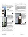
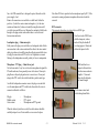
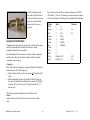
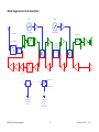
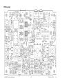
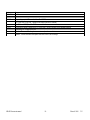
The MKARS 80
QRP 80M transceiver
Construction and user manual
Author - Steve Drury G6ALU
List of contents
Section
no.
1. Specifications
2. Introduction
3. Construction
4. General construction practice
5. Component placement
6. Initial testing
7. Alignment
8. PCB options
9. Boxing up
10. In use
11. Plug and socket fitting instructions
12. Component Identification
13. Fault finding
14. Block diagram and circuit description
15. Circuit diagram
16. PCB overlay
17. Change log
MKARS 80 construction manual
Page
2
2
3
3
4
11
12
13
14
15
16
18
20
22
24
25
26
-1-
Released 5-10-08
V1.2
Introduction
Features
•
•
•
•
•
•
As significant interest had been shown by Milton Keynes Amateur
Radio Society members for a transceiver construction project, I
decided to produce a kit for the Epiphyte originally designed by the
QRP club of British Columbia. Unfortunately this design used several
obsolete components, whilst searching around I became aware of the
BITX20 designed by Ashhar Farhan. The BITX20 is a low technology
transceiver designed to use “simple” components and is easily
adapted to other bands, I quickly manufactured a variant for 80M
(version 1). The radio presented here is a development of that; now at
version 3.
Full 80M LSB coverage
> 5 Watts output power
Frequency display with “Huff and Puff” circuit
Modulation monitor – helps stop over modulation
Volt meter – useful for battery operation
Reverse polarity protection (fuse protected)
Typical Specifications (13.8V supply)
Operating Frequency
RF output
Sensitivity
IF frequency
Audio output
Current consumption
-
Supply voltage
-
3.5 – 3.8 MHz
>5W
MDS better than 1 uV
9.999 MHz
Approximately 0.5W
Receive 120 mA (no signal), Transmit
1.2 amps
10 – 16V
Microphone
Loudspeaker
-
Low cost electret type
8 Ohm (will work into 4 Ohm)
MKARS 80 construction manual
Many changes have been made through my experience with the first
prototype, the original design philosophy was to keep the radio very
simple and basic but I quickly appreciated the benefits of a frequency
read-out and “Huff and Puff” VFO stabilisation. The original design
didn’t have an RF gain control so would overload very easily with the
large signals on 80M, the volume potentiometer was therefore moved
to the front of the receiver becoming an RF gain control.
Another requirement was for all components to be mounted on to one
PCB, keeping wiring to a minimum and PCB cost low. The prototype
used Toko coils but many of these are now hard to obtain so either
fixed inductors or inductors using readily available and low cost cores
have been used throughout.
-2-
Released 5-10-08
V1.2
Construction
These instructions have been targeted at those with some construction
experience and who can identify the different components. Where out
of the ordinary parts have been used a short description follows the
component value.
All components except for the display, its socket and modulation LED
are mounted on the component side of the board. The PCB silk-screen
gives the component locations, in cases where this is difficult to read
please refer to the printed overlay that is larger than actual size. Note
that components are numbered from left to right then top to bottom of
the board. If you have difficulty in locating a component position
place a straight edge across the overlay and look along its length, in
this way components will be easy to locate.
The PCB has been designed to accommodate the components supplied
so if it doesn’t easily fit ask yourself if it belongs there!
General construction practice
Leaded or lead-free cored solder may be used, the solder must be
designed for electronics –
do not use plumbers solder
or additional flux, as the
flux is very corrosive. I use
22SWG (0.7mm) multi-core
type solder that seems most
suitable for this type of
work. A double sided plated
through hole (PTH) PCB
has been used, this has the
advantage of greater
stability and makes dry
MKARS 80 construction manual
-3-
joints very unlikely; however incorrectly fitted components can be
very difficult to remove so it’s important to fit them in the right place
first time! If a component is inadvertently fitted incorrectly it is easiest
to cut off its leads, apply the soldering iron and pull them out from the
topside. A small solder sucker or de-solder braid can be used to clear
the holes out ready for a replacement component to be fitted. When
soldering the component leads it will be noticed that the solder
“wicks” up the hole through to the top surface, this is normal.
For a start place just a few components in place before soldering them,
as experience grows you may find it more productive to fit a larger
number at a time. As each component is fitted put a mark in the box
provided, it’s very easy to forget the last component fitted especially if
you are distracted. If you make use of the component overlay you will
find it helpful if components are highlighted as they are fitted.
Components are taken from one bag at a time keeping the others
sealed, some component types are split between several bags so
indistinguishable parts
don’t become confused
(especially zener diodes
and trimmer capacitors).
Everyone has their
preferred method of
retaining components prior
to soldering; I pull the
leads through with long
nose pliers and put a bend
in the component lead to
stop it falling out of the
board. A good policy is not
to crop leads until they have been soldered, this should stop you from
missing any soldered joints. As this is a PTH board leads can be
cropped quite close to the PCB without damaging the soldered joint.
Released 5-10-08
V1.2
Note that the PCB shouldn’t be cleaned with solvents as residue may
enter the trimmer capacitors and any surface treatment designed to aid
soldering will be removed.
Where possible fit the
components so their values
are easily readable. Some
components MUST be
fitted in the correct
orientation as they are
polarised; this will be
indicated in the text. Save
all the cropped leads, as
some will be needed to fit
the display later in
construction and may also
be used as test loops.
22R Resistor (Red, Red, Black, Gold)
R16
R19
R57
R87
56R Resistor (Green, Blue, Black, Gold)
R1
100R Resistor (Brown, Black, Brown, Gold)
R32
R33
R44
R45
R52
R61
R69
R71
R83
R88
R92
R48
R81
220R Resistor (Red, Red, Brown, Gold)
R7
R14
R55
R58
R63
R66
R68
R77
R84
R86
R93
R96
R60
R82
The components are packed in six bags, each bag contains a list of
contents which will show any substitutions that have been made.
470R Resistor (Yellow, Violet, Brown, Gold)
R25
R70
R90
Component placement
1k Resistor (Brown, Black, Red, Gold)
R3
R6
R9
R13
R26
R34
R38
R39
R50
R51
R53
R65
R73
R78
R79
R80
R94
R95
Resistors are quite small and are identified by four or five colour
bands; if in doubt use a multi-meter to confirm their value.
From bag 1 fit the following components:
R18
R47
R67
R85
4R7 Resistor (Yellow, Violet, Gold, Gold)
R10
R89
10R Resistor (Brown, Black, Black, Gold)
R8
R24
R36
R46
R72
MKARS 80 construction manual
R62
-4-
Released 5-10-08
V1.2
2k2 Resistor (Red, Red, Red, Gold)
R22
R37
R43
R54
R91
100pF NP0 Ceramic (Marked 101)
C45
R75
Be careful not to mix the 4K7 and 47K resistors, these two values are
often confused.
The orientation of trimmer capacitors is marked by the PCB legend,
its best to fit as directed so that the adjustment screw is at ground
potential.
4k7 Resistor (Yellow, Violet, Red, Gold)
R15
R20
R49
R74
10k Resistor (Brown, Black, Orange, Gold)
R5
R11
R17
R28
R56
5.5 - 30pF Open trimmer (Non-enclosed trimmer capacitor)
C103
R40
Zener diodes are polarised – that is they can only be fitted one way
round, there is a band on one end of the glass envelope which should
match up with the band marked on the overlay.
47k Resistor (Yellow, Violet, Orange, Gold)
R12
R41
R42
R64
2V7 400mW Zener diode
D7
100k Resistor (Brown, Black, Yellow, Gold)
R4
180k Resistor (Brown, Grey, Yellow, Gold)
R27
R30
R31
R35
All the following components are taken from bag 2.
R76
The following resistors are metal film close tolerance types with the
value marked as 5 coloured bands.
12k 1% Resistor (Brown, Red, Black, Red, Brown)
R21
10pF Ceramic (10)
C42
C46
C90
22pF Ceramic (22)
C73
68pF NPO Ceramic (68)
C47
33k 1% Resistor (Orange, Orange, Black, Red, Brown)
R23
MKARS 80 construction manual
1nF Mylar (Marked 2A102J)
C59
C60
-5-
Released 5-10-08
V1.2
100pF Ceramic (101)
C31
C48
C80
C104
C55
C67
Axial inductors have a similar appearance to resistors but larger in
size, if measured by a multi-meter they will read a very low resistance.
C76
18uH Axial inductor (Brown, Grey, Black, Silver)
L6
L7
L9
120pF Ceramic (121)
C66
C69
C71
220pF Ceramic (221)
C74
C75
C84
Fit the following components from bag 3
33V 400mW Zener diode
D4
D5
390pF Ceramic (391)
C7
C40
100nF Ceramic (104)
C1
C3
C11
C12
C25
C26
C32
C36
C49
C51
C61
C62
C77
C81
C87
C88
C93
C94
C98
C99
C105
470pF Ceramic (471)
C8
C41
560pF Ceramic (561)
C17
C20
C34
1nF Ceramic (102)
C15
C56
C22
C28
C33
C70
C78
C106
9-50pF NPO Enclosed trimmer (Orange plastic body)
C38
C5
C23
C29
C43
C53
C65
C85
C91
C96
C101
C9
C24
C30
C44
C58
C72
C86
C92
C97
C102
10uH Axial inductor (Brown, Black, Black, Silver)
L8
9-50pF Open trimmer (Non-enclosed trimmer capacitor)
C54
C68
C79
C83
Winding the inductors and transformers
This is probably the trickiest part of the build although with a little
care is not too difficult. The thickest wire has the lowest SWG
number; 38 SWG is the thinnest, 22 SWG the thickest. Fit all the
5V6 400mW Zener diode (markings are indistinct)
D1
MKARS 80 construction manual
C4
C16
C27
C37
C52
C64
C82
C89
C95
C100
-6-
Released 5-10-08
V1.2
toroid inductors vertically against the PCB, refer to the photo of
finished radio.
T4, T5 and T6 – These transformers
are trifilar wound, that is 3 wires are
wound through the ferrite core at the
same time.
First cut three pieces of 38 SWG wire
(the thinnest supplied) about 30cm
long and at one end tightly twist all
three together for about 12mm, snip the end off and solder together –
this will make it easier to thread the wires through the ferrite core.
The remaining length may be
lightly twisted to stop it getting
tangled.
Thread the soldered end
through one of the holes of a
BN43 – 2402 core (the
smallest core, see photo) leaving about 10cm remaining then thread
the wire back through the other hole – this is one complete turn. Loop
the soldered end through a further 4 times to make a total of 5 turns.
Trim the wires back to about 50mm in length, splay apart and tin the
ends with solder.
Now the ends of each of the
three wires has to be identified.
To do this use a multi-meter on
the ohms or continuity range,
when the first wire has been
identified bend it backwards
out of the way. Locate the
MKARS 80 construction manual
-7-
second wire, trim these two ends to about 30mm in length, and now
confirm the last two ends belong to the third wire and crop to about
15mm in length. These wires are then passed through the PCB longest
first and shortest last, anchor the transformer into the PCB by bending
4 wires over against the board. Trim the remaining 2 wires to just a
few mm in length and solder in place; be careful to make sure that the
enamel burns away and the wire tins properly. Once the first two
wires have been soldered in place the other four may be cropped and
soldered. After the radio has been completed (and tested) the
transformers may be fixed into position with a little non-acidic silicon
adhesive, note that bathroom sealer is not suitable as it exudes acetic
acid whilst curing. The correct adhesive doesn’t have any smell.
BN43–2402 5T Trifilar wound 38 SWG ECW
T4
T5
T6
T1 and T3 – these have two windings, each
with 5 turns of 38 SWG wire. First wind 5
turns through the core from one end of the
transformer and crop the leads at 20 –
40mm in length then turn the transformer
round and repeat with another 5 turns from
the other end. It is easiest to tin these wires
before fitting the transformer to the PCB.
BN43–2402 5T+5T 38 SWG ECW
T1
T3
Released 5-10-08
V1.2
T2 is wound using the same method as for T1
and T3 but the windings have three turns of 22
SWG wire on the larger BN43-0202 core.
L2 is wound in a similar way with the same 27 SWG wire but has a
total of 32 turns. Keep the turns tight but it doesn’t matter if several
turns overlap.
L5 – use approximately 50cm of 33 SWG wire and wind using the
same procedure as the other toroid cores with a total of 40 turns,
space the wires evenly around the core.
BN43–0202 3T + 3T 22 SWG ECW
T2
T37-6 30T 27 SWG ECW
L1
L4
L3 – wind 2 turns of 27 SWG wire through the holes
of a BN43-2402 core and tin the leads.
T37-6 32T 27 SWG ECW
L2
T37-6 40T (4.8uH) 33 SWG ECW
L5
BN43-2402 2T 27 SWG ECW
L3
L1 and L4 – Cut off approximately 40cm of 27
SWG wire and pass half of it through the center
of a T37-6 core, this counts as the first turn.
Now wind a further 14 turns through the core
using one end of the wire, turn the core over and
wind the other end through the core 15 times
making a total of 30 turns. Whilst winding pull
the wire tight so the turns lay touching each
other. Crop the wires to 10 – 20mm in length
and tin the ends with solder.
MKARS 80 construction manual
-8-
Electrolytic capacitors are polarised so may only be fitted one way
round. By convention the PCB is marked with a + symbol, the + lead
of a capacitor is longest, the capacitor sleeve is also normally marked
-. Fit the capacitors against the PCB with zero lead length but don’t
put excessive force on the leads as this can make the electrolyte leak
out.
1uF 63V Electrolytic
C10
C13
C21
C35
C39
10uF 25V Electrolytic
C50
47uF 16V Electrolytic
C14
C18
C63
Released 5-10-08
V1.2
BC337 Transistor (Marked C337-40)
Q3
220uF 25V Electrolytic
C2
C6
C19
BC547 Transistor (Marked BC547)
Q2
Q4
Q6
Q7
Q10
Q11
Q12
Q13
Q15
Q16
Q17
Q18
Q22
Fit the following from bag 4.
IC3 and IC4 have 3 legs and look like small transistors.
78L05
IC3
MPSH10 Transistor
Q9
Q19
78L08
IC4
ZTX651 Transistor
Q5
Diodes are polarised devices so can only be fitted one way round,
match the band on one end of the encapsulation with the bar printed
on the PCB.
D8
D13
D18
D9
D14
D19
100R Multi-turn preset resistor
R59
10k Miniature preset resistor
R2
R29
D10
D15
D20
Set R2 fully ANTI-CLOCKWISE and R29 fully CLOCKWISE.
Fit 18 pin socket to IC2 position with notch to match indication on
PCB.
1N5401 Diode
D3
Break the 10 pin single in line header strip into two parts, one of 4
pins and the other 6 pins. Fit to UNDERSIDE of PCB, and solder
connections on component side.
Transistors should be fitted so their outline matches that printed on
the PCB.
MKARS 80 construction manual
Q20
Fit Q5 with approx 2mm spacing to the PCB.
LM386N-1
IC1
1N4148 Diode
D2
D6
D11
D12
D16
D17
Q8
Q14
Q21
-9-
Released 5-10-08
V1.2
Fit 2 fuse clips noting they should be fitted the correct way round due
to fuse locating “tangs”.
Crystals XTAL 2 – 5 require their cans grounding, before fitting the
crystals solder a short length (5 – 6cm) of tinned copper wire (or a
tinned piece of 22 SWG ECW) to the pad provided adjacent to XTAL
2.
10MHz HC49U Crystal (Marked ACT W6)
XTAL
XTAL
XTAL
XTAL
1
2
3
4
Mono 3.5mm jack socket
CON2
PCB Mount BNC socket
CON3
2.1mm DC Socket
CON4
XTAL
5
Relay, BT type
RLY1
Solder already fitted grounding wire to crystal cans and trim off
excess – see photo of completed PCB.
Fit Q1 into the PCB as far as possible – note the orientation shown on
the PCB overlay. Do not crop the leads right down to the PCB, leave
about 5mm so the transistor position can be adjusted if required when
fitting in to a case.
IRF510 FET
Q1
Fit the following parts from bag 5, ensure all the sockets are fitted
flush to the PCB with no gaps underneath.
Before fitting VR1 and VR2 cut the shafts
to required length, if using the suggested
case the shafts need to be cut so that
18mm is left protruding above the
mounting thread.
Note that shaft length will depend on the
types of knobs used. Save the pieces of
shafts removed so one can be used to later
extend the tuning spindle. Fit from the
component side and connect to the PCB
with pieces of cropped component
leads.
Stereo 3.5mm jack socket
CON1
MKARS 80 construction manual
- 10 -
Released 5-10-08
V1.2
4k7 Linear potentiometer
VR1
10k Linear potentiometer
VR2
Fit the tuning capacitor using M2.5 x
6mm screws. NOTE: screws must
have nuts fitted underneath their heads
before fitting so as screw thread
doesn’t foul the capacitor vanes.
Connect the loudspeaker.
Connect 12 – 14V and
check for any obvious fault
symptoms – loud noises or
smoke! Assuming all is OK
measure the 5V regulated
supply at R34 (see photo), it
should be 5 ± 0.25V and the
8V regulated supply at VR2
which should be 8 ± 0.4V.
If either is incorrect remove
power and investigate the
problem before continuing.
Dual gang Polyvaricon
C57
Fit LED from track side and solder on component side, leave the
leads long as the LED will require repositioning when the case is
fitted. The longest lead is the anode (+) terminal.
3mm Red LED
LED 1
Fuse 2A QB
F1
Initial testing
If necessary wire up the power, speaker, microphone and antenna
leads as shown in section 16. Whilst testing it is best to power the
MKARS 80 from a current limited 12 – 14V power supply, on TX a
nominal current of about 1.3 Amps is required.
MKARS 80 construction manual
Before connecting power make a careful inspection of soldered joints
especially for any solder splashes etc. At this point the microcontroller and display should not be fitted as these components can
easily be damaged by wrong voltages applied to their pins. Measure
between supply positive and ground with a multi-meter on Ohms
range to ensure there is not a short circuit, typical values will fall in
the range 1k6 to 2k0. Note that if you reverse connect the meter IE
red lead to ground and black lead to positive the reverse protection
diode resistance will be measured. Make sure R2 is set fully anticlockwise.
- 11 -
Connect an antenna and advance the RF gain. Depending upon band
conditions and the gain of the antenna there should be either stations
or noise heard, the RF gain may need to be advanced fully clockwise
to hear noise when the band is “poor”. If all is OK remove the power
and fit the micro-controller.
Released 5-10-08
V1.2
plastic insulating sheet under the display to guard against any
accidental short circuits.
PIC16F818-I/P
IC2
Now install the display; firstly fit the display using a single screw in
its top left hand corner – a M2.5 x 12mm screw is passed through
from the PCB component side and held in place with a nut. On to this
is screwed another nut, the display and finally another nut. Note that
the PCB spacers supplied are 12mm long this means the display
MUST not be higher than 12mm above the PCB or it will be pressed
against the case causing damage. When you are happy with the
distance pass pieces of tinned copper wire through the display
connections and push them into the socket strip beneath, the LCD
should be moved so the left most holes align. Straighten the display
(compare its top edge with the edge of the PCB) and solder them to
the display. This will make the display pluggable which is desirable
so soldered joints underneath can be accessed.
PC1602F LCD Display
DISP1
Re connect 12V and adjust R29 display bias – whilst monitoring the
LCD display slowly turn R29 anti-clockwise until the background
extinguishes leaving just the characters.
The display should first show a welcome message followed by the
frequency and supply voltage.
Alignment
Set the VFO frequency range; the UK 80M allocation is 3.5 –
3.8MHz. As viewed from the front (track side) turn the Polyvaricon
(C57) knob fully clockwise (minimum frequency) and adjust C38 so
the frequency displayed is
just a little lower than the
lower band edge –
3.450MHz is suggested.
Turn the Polyvaricon
(VFO) to maximum
frequency and check that it
is possible to tune above
the top of the band. If
desired the total tuning
range can be adjusted with
a trimmer capacitor on the
back of the Polyvaricon.
Moving the capacitor into mesh will reduce the range and moving out
of mesh will increase the range – note that after adjusting this
capacitor the frequency will need adjusting by C38.
Look between the display and main PCB and confirm that there are
no wires shorting between the two, you may wish to fit a cardboard or
MKARS 80 construction manual
- 12 -
Released 5-10-08
V1.2
C83 BFO – there are two methods of adjusting the BFO frequency,
either are acceptable.
1. Using a frequency counter adjust C83 for a frequency of
9.9999MHz measured at TP 10MHz.
2. Accurately tune to an SSB transmission on a known frequency
and adjust C83 for a properly resolved signal.
not modulated by the microphone, alternatively plug in a stereo jack
with all contacts grounded.
C54, C68 and C79 band pass filter – the setting of these capacitors is
not critical and may be set as shown in the photo.
R2 PA bias current –
disconnect the antenna and
connect a dummy load
suitable for 5 Watts.
Connect an ammeter in
series with the radio and
power supply capable of
reading 3 amps. Whilst
making this adjustment do
not speak or make other
noises into the
microphone; press the
PTT and note the current
drawn. Adjust R2 for an
increase of 50 ± 5mA. For
example, before adjustment (R2 fully anti-clockwise) the current was
230mA, in this example when correctly adjusted the current will be
275 – 285mA. Note as the components warm up that the current will
rise – do not transmit for more than a few seconds if Q1 isn’t fitted
with a heatsink or it will overheat.
R59 and C103 mixer balance – connect a sensitive power meter and
dummy load to the antenna connector. With power connected slowly
insert the microphone / PTT plug until the transmitter is operated but
MKARS 80 construction manual
- 13 -
A small reading may be noted on the power meter, adjust R59 to
reduce this to zero. There are two possible methods to further
improve the mixer balance:
1. Tune in to the carrier with another radio and adjust R59 and
C103 for minimum signal or “S” meter reading.
2. Connect an oscilloscope to the antenna connector and adjust R59
and C103 for minimum waveform, note that both these
adjustments are inter-reactive (they effect each other).
PCB Options
Power switch
The PCB incorporates a
facility for fitting a power
switch, the RF gain control
may be replaced by a
switched 4k7 linear
potentiometer and the
power switch wired to the
marked pads. For the switch
to function the track needs
to be cut with a sharp knife
where indicated.
Internal Loudspeaker
A small internal loudspeaker can be fitted, it is best to position this
away from L5 to avoid the magnet de-tuning the VFO. Connections
are provided for the loudspeaker (the polarity being unimportant), the
internal loudspeaker will be disconnected when the external speaker
socket is used.
Released 5-10-08
V1.2
Internal battery
PCB pads are provided for connecting an internal battery if desired,
the negative terminal is isolated when an external power source is
plugged in; note that there is no provision
to recharge internal batteries.
Boxing up
Fit 4 M3 x 12mm hexagonal spacers to
the corners of the PCB, a flat and
serrated washer should be fitted under
each nut.
Cut the knob extension to length and fit
to the tuning capacitor shaft, this is a
short length of plastic air pipe, it allows
one of the cut-off potentiometer shafts to
be used to extend the Polyvaricon shaft.
Don’t force too much tube over the shaft
as the pressure required could damage
the capacitor.
A metal case must be used for screening
and to provide Q1 with a heatsink.
Print out the drilling template and
confirm the size is correct by measuring
the printed dimensions. Stick the drilling templates to the outside of
the case aligning the reference edges with the INSIDE surfaces of the
box, this is important; for the templates to be universal no account has
been made for case thickness, instructions are printed on the
templates. Possible adhesives are PVA glue and double-sided tape.
MKARS 80 construction manual
- 14 -
Drill all holes to the sizes indicated on the template, use good
engineering practice; start with a small drill and work up in size. Note
the following:
• If the recommended case is being used the control shaft and BNC
connector holes will need to be elongated to allow the PCB to fit.
• Ensure that when plugged in the DC connector outer contact can’t
touch the case.
• If the PA transistor-mounting hole doesn’t align properly it is
permissible to open the hole up slightly, if stressed the transistor
legs will fail sometime in the future.
To cut the display window
without special tools I
would recommend drilling
many holes close to each
other just on the inside of
the window then using a
pair of side cutters join
them up. The window can
then be squared up using a
file.
When all holes have been
cut, trial fit the board to the case and if necessary re-heat the solder
pads on Q1 (PA transistor) to align its mounting hole with that drilled
in the case.
Released 5-10-08
V1.2
Note that when fitting the PA transistor into the case a heatsink
washer and insulator must be used; place the insulator (no thermal
compound is required) between transistor tab and case, fit plastic
insulator through tab of transistor and into hole in case. Then fit an
M3 x 10mm screw from the outside of the case and secure with flat
washer, serrated washer and M3 nut; see photo.
2. A negative image is provided, this can be printed on to acetate or a
bubble jet transparency, by reversing the image the non-printed
side is nearest the user so protecting the writing.
The builder is encouraged to personalise the front to their own taste to
add some individuality.
I
The PCB is secured in place by 4 M3 x 6mm screws with flat washers
under the heads. Secure the BNC to the case using the serrated washer
and nut supplied. Fit three knobs as required, note the shafts are 6mm
in diameter.
have catered for two methods of fitting a front panel; with a little
thought I’m sure there are many more. For those wanting to design
their own front panel critical hole dimensions and spacing are given
on the drilling template.
Final air test
Attach an antenna and arrange a contact with a local amateur on the
80M band to confirm the radio operates as expected.
1. A PDF file of a front panel is provided, this may be printed and
glued (double sided tape perhaps) to the front and then covered
with a sheet of acetate / overhead projector film trapped under the
four fixings screws.
Firstly it should be remembered that the MKARS80 is low cost and of
a relatively simple design, its functionality cannot be compared with a
complex commercial transceiver! That said great enjoyment can be
had if its limitations are realised.
MKARS 80 construction manual
- 15 -
In use
Released 5-10-08
V1.2
After powering on best frequency stability isn’t reached until the
temperature within the case has stabilised, the Huff and Puff circuit
will keep the radio on tune in the short term but may need adjusting a
few times during the warm up period.
Tuning
The VFO is capable of covering the whole UK 80M allocation but due
to the VFO frequency being below that of the IF the tuning works
backwards. I.e. clockwise rotation decreases the tuned frequency. Once
the approximate frequency has been tuned with the main tuning
control the fine tune control may be used to get within ±25Hz of the
wanted frequency.
It will be noticed that the Huff and Puff circuit will try to hold the
frequency as you adjust the fine tune control, this “hold” will be
broken when the actual frequency is more than about 100 Hz different
from that displayed. Once the lock is broken there will be a delay of 8
seconds before the Huff and Puff again tries to hold the frequency
steady.
The Huff and Puff circuit is able to compensate for about ± 1.5kHz
frequency drift; the position within the lock range is shown by the bar
to the left of the battery voltage. If this tuning bar reaches either of the
extremes the VFO should be re-adjusted. Remember that if the
displayed frequency is more than about 100Hz different from the VFO
frequency the Huff and Puff circuit will stop attempting to correct the
drift and there will be a sudden change in tuned frequency.
RF Gain
The RF gain control determines how much signal is applied to the
receiver, this has the same effect as adjusting the AF gain (volume)
control on a conventional radio. As this simple design doesn’t
MKARS 80 construction manual
- 16 -
incorporate an AGC circuit the control has to be adjusted for a
comfortable listening volume and may need adjustment between
different stations in a QSO.
WARNING
Be carefull when using headphones as volume is dependent on
strength of received signals and at the very least this could
“surprise” the operator when tuning through a local station!
Modulation indicator
This LED extinguishes at about the point the PA transistor saturates;
running the output transistor into saturation can cause “splatter” across
adjacent QSOs. Splatter is actually intermodulation and is caused by
the output stage becoming non-linear and mixing frequencies within
the wanted spectra causing nearby unwanted signals. Whilst
transmitting the indicator should momentarily extinguish on voice
peaks.
Fitting Plugs and sockets
Power connector – 2.1mm DC plug
These are available in two lengths, either is suitable with the case
recommended but the “long” type may be required if the case has thick
walls.
It is very wise to use
colour-coded lead (red
and black) to avoid
any accidents! Use a
lead suitable for
carrying 2 amps; if
running from a battery
it would also be
sensible to fit an inline
Released 5-10-08
V1.2
fuse – the PCB mounted fuse is designed to protect the radio not the
power supply / lead.
Remove the connector cover and slide over both leads. Solder the
positive (+) lead to the center contact and negative (-) to the outer
contact and strain relief, when cool carefully crimp the strain relief
over both wires and fit the cover. Measure the continuity of both leads
through to the plug contacts and confirm there is no short circuit
between inner and outer.
Loudspeaker plug – 3.5mm mono jack
Firstly remove the plug cover and slide over loudspeaker leads. Solder
one connection to the centre contact and the other to the outer contact /
cable grip, when cool carefully crimp the cable grip around both wires
to help give some strain relief. Wire size isn’t important as currents
flowing to the loudspeaker are small, polarity of wires is unimportant.
Microphone / PTT plug – 3.5mm Stereo jack
Use has been made of very low cost electret microphones designed for
PC multi-media use; these generally come with a stereo 3.5mm jack
plug. Remove the jack plug and rewire to a new stereo 3.5mm jack
along with a PTT switch, the switch should be a push to make type.
As with the loudspeaker connector remove the plug cover and slide
over the microphone and PTT switch leads, then solder the wires to
connector solder tabs as follows:
Plug tip
Middle contact
Outer contact
–
–
–
Note that a DC bias is provided on the microphone input by R17, if the
user insists on using a dynamic microphone this resistor should be
removed.
BNC connector
The connector shown here is a typical low cost BNC type.
Over the cut end of RG58 coax
slide the clamp nut, washer,
and seal. Strip the sheath off
over-long (approx. 15mm) and
slide on the tapered collet.
Pull braid back over
tapered collet and trim;
trim the inner conductor
length to 7.5mm and
then strip the dielectric
to 5mm in length.
Fit the inner contact and
solder through small hole.
Microphone +
PTT switch
Microphone and PTT ground
When the soldered joints have cooled, the cable retainer should be
carefully crimped over all wires and the cover screwed in place.
MKARS 80 construction manual
- 17 -
Released 5-10-08
V1.2
Fit body and tighten clamp
nut, finally check that there is
no short circuit between inner
and outer contacts and that
inner contact is in correct
position.
Component identification
Components have been packed in to 6 bags, the contents of these bags
and order of assembly have carefully been chosen so similar
components shouldn’t become confused.
For fault finding it will be necessary to correctly identify components
and their values after the radio has been built; methods of marking
component values are given.
Two resistors used in the battery voltage measurement circuit (R21 –
12K and R23 – 33K) are 1% tolerance types and are therefore marked
with 5 coloured bands; all other types have standard 4 band markings.
Colour
Black
Brown
Red
Orange
Yellow
Green
Blue
Violet
Grey
White
Silver
Gold
Value
0
×1
1
×10
2
×100
3
×1000
4
×10000
5
×100000
6
×1000000
7
8
9
Divide by 100
Divide by 10
Tolerance
1%
2%
10%
5%
Capacitors
Most of the small value capacitors (ceramic and Mylar) used in this kit
are marked in one of the following ways.
• Marked directly with their value, for example 8 for 8pF and 68 for
68pF.
• Marked numerically based in Pico farads, the first two digits are
the value and the third is the multiplier, for example 1nF (1000pF)
is marked 102 (1, 0 and two zeroes), 220pF is marked 221 (2, 2
and one zero).
Electrolytic capacitors are marked directly with their value.
Resistors
Values on all the resistors in this kit use a colour code to indicate
value.
MKARS 80 construction manual
- 18 -
Released 5-10-08
V1.2
Examples:
1kΩ 5% (1000Ω) = Brown (1) Black (0) Red (×100) Gold (5%
tolerance)
2R2 5% (2.2Ω) = Red (2) Red (2) Gold (divide by 10) Gold (5%
tolerance)
Note that 1000Ω = 1k, 1000000Ω = 1M, 2K2 = 2200Ω, 2R2 = 2.2Ω
etc.
Transistors and Ics
Inductors
Axial inductors use the same colour code as resistors with their value
based in micro Henries; for example 8.2uH is marked Grey (8), Red
(2), Gold (divide by 10) and Silver (10% tolerance). All inductors used
are significantly larger than resistors so are unlikely to be confused;
axial inductors only have one failure mode – open circuit, which can
easily be identified with a multi-meter set to measure resistance.
Diodes
All diodes used are axial and have their cathode end marked by a
”band” on the encapsulation.
TO92 and E-line terminal identification
Component
BC337
BC547
MPSH10
ZTX651
78L05
78L08
Lead identification
1
2
3
Emitter
Base
Collector
Emitter
Base
Collector
Collector
Emitter
Base
Emitter
Base
Collector
Input
Gnd
Output
Input
Gnd
Output
IRF510 FET terminal identification.
Values are marked on the bodies although for the small glass diodes
(zener diodes and 1N4148 types) they will be hard to read without a
magnifying glass.
MKARS 80 construction manual
- 19 -
Released 5-10-08
V1.2
LM386 is similar to PIC16F818 but only has
8 pins.
Fault finding
Most faults are due to poor soldered connections or components
misplaced, it is very rare to be supplied with a faulty component.
Before making any measurements look carefully for any poor soldered
joints, short circuits or incorrectly fitted components.
Should fault finding be necessary a table of voltages is given below,
transistor voltages were measured both in transmit and receive.
MKARS 80 construction manual
- 20 -
Released 5-10-08
V1.2
Voltage tables
Q1
Gate
0
Receive
Drain
13.8
Source
0
Gate
3.4*
Transmit
Drain
13.8
Source
0
Q2
Q3
Q4
Q5
Q6
Q7
Q8
Q9
Q10
Q11
Q12
Q13
Q14
Q15
Q16
Q17
Q18
Q19
Q20
Q21
Q22
Emitter
0
0
0
0
0
0
0
0
0
3.6
3
4
0
2.2
3.9
3.75
4.2
3
0
0
0
Base
0
0
0
0
0.65
0.39
0.57
0
0
3.6
3.65
4.65
0.62
2.8
4.1#
4.4
4.3
3.7
0
0
0
Collector
0
0
0
0
0.65
2.2
2.2
0
0
7.5
7.5
9.4
4.4
9
7.2
12.8
7.2
7.6
0
0
0
Emitter
0
0
3.7
1.6
0
0
0
2.4
2.8
3.6
3
4
0
0
3.9
0
4.2
0
2.9
2.1
2.5
Base
0.63
0.73
4.4
2
0.65
0.39
0.57
3.2
3.4
3.6
3.65
4.6
0
0
4.1#
0
4.3
0
3.7
2.8
3.2
Collector
4.4
0
12.3
12
0.65
2.2
2.2
11
3.8
7.5
7.5
9.3
0
0
7.2
0
7.2
0
7.50
9
10.2
Transistor
IC number
IC1
IC2
IC3
IC4
1
1.4
4.9
13.8
13.0
2
0
0
0
0
3
0
0
5
8
Pin number
4
5
6
7
8
9
10
11
0
7
13.8 7
1.4
0
0
5
0
0
2.5
4.9
4.9
All IC pin voltages are similar during transmit or receive
12
13
14
15
16
17
18
2.2
4.9
5
-0.3
2.2
3.7
0
Notes:
• Value will depend on setting of bias control
# Measuring this point can affect circuit operation leading to false readings
All measurements were made with RF gain at minimum and no modulating audio
MKARS 80 construction manual
- 21 -
Released 5-10-08
V1.2
Block diagram and circuit description
3.5 - 3.8 MHz
VFO
BFO
6.5 - 6.2 MHz
10.000150 MHz
Audio mute
Cut off 4MHz
Center
frequency
9.999 MHz
3.5 - 3.8 MHz
3.5 - 3.8 MHz
0.05 mW
Receive 12V
12V
8V
12V
Transmit 12V
8V regulator
for oscillator
stages
MKARS 80 construction manual
Transmit /
receive power
switching part of
antenna relay
- 22 -
Released 5-10-08
V1.2
The radio uses a single IF super-heterodyne architecture with
several so called bi-directional stages. These allow the sharing of
all the main functional blocks between transmit and receive –
mixers, IF filter VFO and BFO.
Frequency display and “Huff and Puff”
A micro-controller “counts” the VFO oscillations with a 40mS
time base derived from the BFO, a correction voltage is also
derived form the comparison of the counted down VFO input and
the internally generated 40mS time base. The correction voltage
is generated by an internal PWM (pulse width modulator) and
after filtering is applied to a varicap diode (actually a zener used
as a varicap) in the VFO section.
Receive signal flow
The receive signal passes through the transmit low pass filter, the
switching relay, RF gain control and then through a high pass
filter; in this way a receive band pass filter is not required.
Filtered an attenuated signal is then amplified and presented to a
double balanced mixer constructed from discrete components,
this mixer is also shared with transmit. By mixing the received
signal with 6.5 – 6.2 MHz from the VFO an IF of 10 MHz is
generated. Note that the VFO works backwards, a 3.5 MHz tuned
frequency requires a VFO frequency of 6.5 MHz and a tuned
frequency of 3.8 MHz requires a VFO frequency of 6.2 MHz.
An A/D input of the micro-controller is used to measure and
indicate supply voltage via the LCD display.
The amplified IF signal is then filtered by a 4-pole crystal filter at
9.999 MHz before again being amplified and presented to the
BFO mixer. When the IF signal is mixed with the output from the
BFO an audio signal is produced, this is then amplified and
supplied to the loudspeaker. A mute circuit operates in transmit to
avoid feedback between microphone and loudspeaker.
Transmit signal flow
Audio from the microphone is first amplified and then fed to the
BFO or carrier insertion oscillator, the frequency spectra
generated is first amplified and then filtered by the IF filter shared
with the receiver.
Amplified IF signal is presented to the main mixer where it is
translated to the output frequency again amplified and then
filtered by the band pass filter. Three more stages of amplification
follow before the signal is passed through the transmit / receive
relay then through the low pass filter to the antenna.
MKARS 80 construction manual
- 23 -
Released 5-10-08
V1.2
Circuit Diagram
MKARS 80 construction manual
- 24 -
Released 5-10-08
V1.2
PCB overlay
MKARS 80 construction manual
- 25 -
Released 5-10-08
V1.2
Version
12-05-07 V1.0
Changes
First release
15-06-07
Voltage reading on pin 8 of IC1 corrected (thanks to Tom G3LMX)
C42, C46 now 10pF, L8 now 10uH – Component value changes required due to availability
T1 and T3 shown as 2T+2T, should be 5T+5T
Moved position in manual for adjustment of R29 LCD bias voltage – previously positioned at end of alignment instructions
Modify fitting LCD – left most holes are used
Adjustment of bias current R2 – changed measurements in example to be more realistic
Schematic – Corrected connections on microphone socket in line with PCB (no PCB changes)
05-10-08
MKARS 80 construction manual
- 26 -
Released 5-10-08
V1.2