1
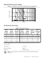
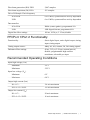
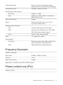
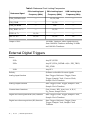
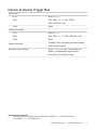
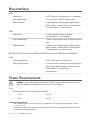
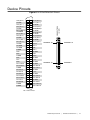
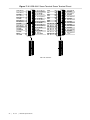
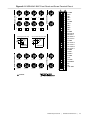
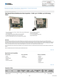
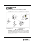
DEVICE SPECIFICATIONS
NI 6341
X Series Data Acquisition: 500 kS/s, 16 AI, 24 DIO, 2 AO
Français
日本語
Deutsch
한국어
简体中文
ni.com/manuals
The following specifications are typical at 25 °C, unless otherwise noted. For more
information about the NI 6341, refer to the X Series User Manual available at ni.com/manuals.
Analog Input
Number of channels
8 differential or 16 single ended
ADC resolution
16 bits
DNL
No missing codes guaranteed
INL
Refer to the AI Absolute Accuracy section.
Sample rate
Single channel maximum
500 kS/s
Multichannel maximum (aggregate)
500 kS/s
Minimum
No minimum
Timing resolution
10 ns
Timing accuracy
50 ppm of sample rate
Input coupling
DC
Input range
±0.2 V, ±1 V, ±5 V, ±10 V
Maximum working voltage for analog inputs
(signal + common mode)
±11 V of AI GND
CMRR (DC to 60 Hz)
100 dB
Input impedance
Device on
AI+ to AI GND
>10 GΩ in parallel with 100 pF
AI- to AI GND
>10 GΩ in parallel with 100 pF
Device off
AI+ to AI GND
1,200 Ω
AI- to AI GND
1,200 Ω
Input bias current
±100 pA
Crosstalk (at 100 kHz)
Adjacent channels
-75 dB
Non-adjacent channels
-90 dB
Small signal bandwidth (-3 dB)
1.2 MHz
Input FIFO size
2,047 samples
Scan list memory
4,095 entries
Data transfers
PCIe/PXIe
DMA (scatter-gather), programmed I/O
USB
USB Signal Stream, programmed I/O
Overvoltage protection for all analog input and sense channels
Device on
±25 V for up to two AI pins
Device off
±15 V for up to two AI pins
Input current during overvoltage condition
±20 mA max/AI pin
Settling Time for Multichannel Measurements
Accuracy, full-scale step, all ranges
2
|
±90 ppm of step (±6 LSB)
2 μs convert interval
±30 ppm of step (±2 LSB)
3 μs convert interval
±15 ppm of step (±1 LSB)
5 μs convert interval
ni.com |
NI 6341 Specifications
Typical Performance Graph
Figure 1. Settling Error versus Time for Different Source Impedances
Error (ppm of Step Size)
10 k
2 kΩ
10 kΩ
1k
1 kΩ
100
≤ 100 Ω
5 kΩ
10
1
10
100
Time (μs)
AI Absolute Accuracy
Table 1. AI Absolute Accuracy
Nominal
Range
Positive
Full Scale
Nominal
Range
Negative
Full Scale
Residual
Gain Error
(ppm of
Reading)
Residual
Offset
Offset
Tempco
Error (ppm
(ppm of
of Range) Range/°C)
Random
Noise, σ
(μVrms)
Absolute
Accuracy at
Full Scale
(μV)
10
-10
65
13
23
270
2,190
5
-5
72
13
23
135
1,130
1
-1
78
17
26
28
240
0.2
-0.2
105
27
39
9
60
For more information about absolute accuracy at full scale, refer to the AI Absolute Accuracy
Example section.
Gain tempco
7.3 ppm/°C
Reference tempco
5 ppm/°C
INL error
60 ppm of range
Note Accuracies listed are valid for up to two years from the device external
calibration.
NI 6341 Specifications |
© National Instruments
|
3
AI Absolute Accuracy Equation
AbsoluteAccuracy = Reading · (GainError) + Range · (OffsetError) + NoiseUncertainity
GainError = ResidualGainError + GainTempco · (TempChangeFromLastInternalCal) +
ReferenceTempco · (TempChangeFromLastExternalCal)
OffsetError = ResidualOffsetError + OffsetTempco · (TempChangeFromLastInternalCal)
+ INLError
NoiseUncertainty =
10,000 points.
Random Noise ⋅ 3
for a coverage factor of 3 σ and averaging
10, 000
AI Absolute Accuracy Example
Absolute accuracy at full scale on the analog input channels is determined using the following
assumptions:
•
TempChangeFromLastExternalCal = 10 °C
•
TempChangeFromLastInternalCal = 1 °C
•
number_of_readings = 10,000
•
CoverageFactor = 3 σ
For example, on the 10 V range, the absolute accuracy at full scale is as follows:
GainError = 65 ppm + 7.3 ppm · 1 + 5 ppm · 10 = 122 ppm
OffsetError = 13 ppm + 23 ppm · 1 + 60 ppm = 96 ppm
NoiseUncertainty =
270 µ� ⋅ 3
= 8.1 μV
10, 000
AbsoluteAccuracy = 10 V · (GainError) + 10 V · (OffsetError) + NoiseUncertainty =
2,190 μV
Analog Output
Number of channels
2
DAC resolution
16 bits
DNL
±1 LSB
Monotonicty
16 bit guaranteed
Maximum update rate (simultaneous)
1 channel
900 kS/s
2 channels
840 kS/s per channel
Timing accuracy
50 ppm of sample rate
Timing resolution
10 ns
Output range
±10 V
4
|
ni.com |
NI 6341 Specifications
Output coupling
DC
Output impedance
0.2 Ω
Output current drive
±5 mA
Overdrive protection
±15 V
Overdrive current
15 mA
Power-on state
±20 mV
Power-on/off glitch
PCIe/PXIe
2 V for 500 ms
USB
1.5 V for 1.2 s1
Output FIFO size
8,191 samples shared among channels used
Data transfers
PCIe/PXIe
DMA (scatter-gather), programmed I/O
USB
USB Signal Stream, programmed I/O
AO waveform modes
Non-periodic waveform, periodic waveform
regeneration mode from onboard FIFO,
periodic waveform regeneration from host
buffer including dynamic update
Settling time, full-scale step, 15 ppm (1 LSB) 6 µs
Slew rate
15 V/µs
Glitch energy
Magnitude
100 mV
Duration
2.6 µs
AO Absolute Accuracy
Absolute accuracy at full-scale numbers is valid immediately following self calibration and
assumes the device is operating within 10 °C of the last external calibration.
1
Typical behavior. Time period may be longer due to host system USB performance. Time period
will be longer during firmware updates.
NI 6341 Specifications
|
© National Instruments
|
5
Table 2. AO Absolute Accuracy
Nominal Nominal Residual
Residual
INL
Absolute
Offset
Range
Range
Gain
Gain
Reference Offset
Error Accuracy
Tempco
Positive Negative
Error
Error
(ppm
at Full
Tempco Tempco
(ppm of
Full
Full
(ppm of (ppm/°C) (ppm/°C) (ppm of
of
Scale
Range/°C)
Scale
Scale
Reading)
Range)
Range)
(μV)
10
-10
80
11.3
5
53
4.8
128
3,271
Note Accuracies listed are valid for up to two years from the device external
calibration.
AO Absolute Accuracy Equation
AbsoluteAccuracy = OutputValue · (GainError) + Range · (OffsetError)
GainError = ResidualGainError + GainTempco · (TempChangeFromLastInternalCal) +
ReferenceTempco · (TempChangeFromLastExternalCal)
OffsetError = ResidualOffsetError + OffsetTempco · (TempChangeFromLastInternalCal)
+ INLError
Digital I/O/PFI
Static Characteristics
Number of channels
24 total, 8 (P0.<0..7>),
16 (PFI <0..7>/P1, PFI <8..15>/P2)
Ground reference
D GND
Direction control
Each terminal individually programmable as
input or output
Pull-down resistor
50 kΩ typical, 20 kΩ minimum
Input voltage protection
±20 V on up to two pins
Caution Stresses beyond those listed under the Input voltage protection
specification may cause permanent damage to the device.
Waveform Characteristics (Port 0 Only)
Terminals used
Port 0 (P0.<0..7>)
Port/sample size
Up to 8 bits
6
|
ni.com |
NI 6341 Specifications
Waveform generation (DO) FIFO
2,047 samples
Waveform acquisition (DI) FIFO
255 samples
DO or DI Sample Clock frequency
PCIe/PXIe
0 to 1 MHz, system and bus activity dependent
USB
0 to 1 MHz, system and bus activity dependent
Data transfers
PCIe/PXIe
DMA (scatter-gather), programmed I/O
USB
USB Signal Stream, programmed I/O
Digital line filter settings
160 ns, 10.24 μs, 5.12 ms, disable
PFI/Port 1/Port 2 Functionality
Functionality
Static digital input, static digital output, timing
input, timing output
Timing output sources
Many AI, AO, counter, DI, DO timing signals
Debounce filter settings
90 ns, 5.12 μs, 2.56 ms, custom interval,
disable; programmable high and low
transitions; selectable per input
Recommended Operating Conditions
Input high voltage (VIH)
Minimum
2.2 V
Maximum
5.25 V
Input low voltage (VIL)
Minimum
0V
Maximum
0.8 V
Output high current (IOH)
P0.<0..7>
-24 mA maximum
PFI <0..15>/P1/P2
-16 mA maximum
Output low current (IOL)
P0.<0..7>
24 mA maximum
PFI <0..15>/P1/P2
16 mA maximum
NI 6341 Specifications
|
© National Instruments
|
7
Digital I/O Characteristics
Positive-going threshold (VT+)
2.2 V maximum
Negative-going threshold (VT-)
0.8 V minimum
Delta VT hysteresis (VT+ - VT-)
0.2 V minimum
IIL input low current (VIN = 0 V)
-10 μA maximum
IIH input high current (VIN = 5 V)
250 μA maximum
Figure 2. P0.<0..7>: IOH versus VOH
0
55 °C; Vdd = 4.5 V
25 °C; Vdd = 5.0 V
0 °C; Vdd = 5.5 V
–5
–10
IOH (mA)
–15
–20
–25
–30
–35
–40
–45
–50
2
3
4
VOH (V)
8
|
ni.com |
NI 6341 Specifications
5
6
Figure 3. P0.<0..7>: IOL versus VOL
40
35
30
IOL (mA)
25
20
15
10
0 °C; Vdd = 5.5 V
25 °C; Vdd = 5.0 V
55 °C; Vdd = 4.5 V
5
0
0
0.2
0.4
0.6
0.8
1.0
1.2
VOL (V)
Figure 4. PFI <0..15>/P1/P2: IOH versus VOH
0
–5
–10
IOH (mA)
–15
–20
–25
–30
–35
55 °C; Vdd = 4.5 V
25 °C; Vdd = 5.0 V
0 °C; Vdd = 5.5
–40
–45
–50
2
3
4
5
6
VOH (V)
NI 6341 Specifications
|
© National Instruments
|
9
Figure 5. PFI <0..15>/P1/P2: IOL versus VOL
40
0 °C; Vdd = 5.5 V
25 °C; Vdd = 5.0 V
55 °C; Vdd = 4.5 V
35
30
IOL (mA)
25
20
15
10
5
0
0
0.2
0.4
0.6
0.8
1.0
1.2
VOL (V)
General-Purpose Counters
Number of counter/timers
4
Resolution
32 bits
Counter measurements
Edge counting, pulse, pulse width,
semi-period, period, two-edge separation
Position measurements
X1, X2, X4 quadrature encoding with
Channel Z reloading; two-pulse encoding
10
|
ni.com
|
NI 6341 Specifications
Output applications
Pulse, pulse train with dynamic updates,
frequency division, equivalent time sampling
Internal base clocks
100 MHz, 20 MHz, 100 kHz
External base clock frequency
PCIe/USB
0 MHz to 25 MHz
PXIe
0 MHz to 25 MHz; 0 MHz to 100 MHz on
PXIe_DSTAR<A,B>
Base clock accuracy
50 ppm
Inputs
Gate, Source, HW_Arm, Aux, A, B, Z,
Up_Down, Sample Clock
Routing options for inputs
PCIe
Any PFI, RTSI, many internal signals
PXIe
Any PFI, PXIe_DSTAR<A,B>, PXI_TRIG,
PXI_STAR, many internal signals
USB
Any PFI, many internal signals
FIFO
127 samples per counter
Data transfers
PCIe/PXIe
Dedicated scatter-gather DMA controller for
each counter/timer, programmed I/O
USB
USB Signal Stream, programmed I/O
Frequency Generator
Number of channels
1
Base clocks
20 MHz, 10 MHz, 100 kHz
Divisors
1 to 16
Base clock accuracy
50 ppm
Output can be available on any PFI or RTSI terminal.
Phase-Locked Loop (PLL)
Number of PLLs
1
NI 6341 Specifications
|
© National Instruments
|
11
Table 3. Reference Clock Locking Frequencies
Reference Signal
PCIe Locking Input
Frequency (MHz)
PXIe Locking Input
Frequency (MHz)
USB Locking Input
Frequency (MHz)
PXIe_DSTAR<A,B>
—
10, 20, 100
—
PXI_STAR
—
10, 20
—
PXIe_CLK100
—
100
—
PXI_TRIG <0..7>
—
10, 20
—
RTSI <0..7>
10, 20
—
—
PFI <0..15>
10, 20
10, 20
10
Output of PLL
100 MHz Timebase; other signals derived
from 100 MHz Timebase including 20 MHz
and 100 kHz Timebases
External Digital Triggers
Source
PCIe
Any PFI, RTSI
PXIe
Any PFI, PXIe_DSTAR<A,B>, PXI_TRIG,
PXI_STAR
USB
Any PFI
Polarity
Software-selectable for most signals
Analog input function
Start Trigger, Reference Trigger, Pause
Trigger, Sample Clock, Convert Clock,
Sample Clock Timebase
Analog output function
Start Trigger, Pause Trigger, Sample Clock,
Sample Clock Timebase
Counter/timer functions
Gate, Source, HW_Arm, Aux, A, B, Z,
Up_Down, Sample Clock
Digital waveform generation (DO) function
Start Trigger, Pause Trigger, Sample Clock,
Sample Clock Timebase
Digital waveform acquisition (DI) function
Start Trigger, Reference Trigger, Pause
Trigger, Sample Clock, Sample Clock
Timebase
12
|
ni.com
|
NI 6341 Specifications
Device-to-Device Trigger Bus
Input source
PCIe
RTSI <0..7>2
PXIe
PXI_TRIG <0..7>, PXI_STAR,
PXIe_DSTAR<A,B>
USB
None
Output destination
PCIe
RTSI <0..7>2
PXIe
PXI_TRIG <0..7>, PXIe_DSTAR<A,B>
USB
None
Output selections
10 MHz Clock, frequency generator output,
many internal signals
Debounce filter settings
90 ns, 5.12 μs, 2.56 ms, custom interval,
disable; programmable high and low
transitions; selectable per input
2
In other sections of this document, RTSI refers to RTSI <0..7> for NI PCIe-6341, or
PXI_TRIG <0..7> for NI PXI-6341.
NI 6341 Specifications |
© National Instruments
|
13
Bus Interface
PCIe
Form factor
x1 PCI Express, specification v1.1 compliant
Slot compatibility
x1, x4, x8, and x16 PCI Express slots 3
DMA channels
8, analog input, analog output, digital input,
digital output, counter/timer 0, counter/timer
1, counter/timer 2, counter/timer 3
PXIe
Form factor
x1 PXI Express peripheral module,
specification rev 1.0 compliant
Slot compatibility
x1 and x4 PXI Express or PXI Express hybrid
slots
DMA channels
8, analog input, analog output, digital input,
digital output, counter/timer 0, counter/timer
1, counter/timer 2, counter/timer 3
NI PXIe-6341 devices may be installed in PXI Express slots or PXI Express hybrid slots.
USB
USB compatibility
USB 2.0 Hi-Speed or full-speed4
USB Signal Stream
8, can be used for analog input, analog output,
digital input, digital output, counter/timer 0,
counter/timer 1, counter/timer 2,
counter/timer 3
Power Requirements
Caution The protection provided by the NI 6341 can be impaired if the device is
used in a manner not described in the X Series User Manual.
PCIe
Without disk drive power connector installed
3
4
14
|
+3.3 V
1.4 W
+12 V
8.6 W
Some motherboards reserve the x16 slot for graphics use. For PCI Express guidelines, refer to
ni.com/pciexpress.
Operating on a full-speed bus results in lower performance, and you might not be able to achieve
maximum sampling/update rates.
ni.com |
NI 6341 Specifications
With disk drive power connector installed
+3.3 V
1.4 W
+12 V
3W
+5 V
15 W
PXIe
+3.3 V
1.6 W
+12 V
19.8 W
Power supply requirements
11 to 30 VDC, 30 W, 2 positions 3.5 mm pitch
pluggable screw terminal with screw locks
similar to Phoenix Contact MC 1,5/2-STF-3,5
BK
Power input mating connector
Phoenix Contact MC 1,5/2-GF-3,5 BK or
equivalent
USB
Caution The NI USB-6341 must be powered with an NI offered AC adapter or a
National Electric Code (NEC) Class 2 DC source that meets the power requirements
for the device and has appropriate safety certification marks for country of use.
Current Limits
Caution Exceeding the current limits may cause unpredictable behavior by the
device and/or the PC/chassis.
PCIe
Without disk drive power connector installed
P0/PFI/P1/P2 and +5 V terminals
combined
1 A max
NI 6341 Specifications
|
© National Instruments
|
15
With disk drive power connector installed
+5 V terminal (connector 0)
1 A max5
P0/PFI/P1/P2 combined
1 A max
PXIe
+5 V terminal (connector 0)
1 A max5
P0/PFI/P1/P2 and +5 V terminals
combined
2 A max
+5 V terminal
1 A max5
P0/PFI/P1/P2 and +5 V terminals
combined
2 A max
USB
Physical Characteristics
Printed circuit board dimensions
PCIe
9.9 × 16.8 (3.9 × 6.6 in.) (half-length)
PXIe
Standard 3U PXI
Enclosure dimensions (includes connectors)
USB
Screw terminal
26.4 × 17.3 × 3.6 cm (10.4 × 6.8 x 1.4 in.)
BNC
20.3 × 18.5 × 6.8 cm (8.0 × 7.3 × 2.7 in.)
Weight
PCIe
104 g (3.6 oz)
PXIe
157 g (5.5 oz)
USB
Screw Terminal
1.406 kg (3 lb 1.6 oz)
BNC
1.520 kg (3 lb 5.6 oz)
I/O connector
PCIe/PXIe
1 68-pin VHDCI
USB
5
16
|
Screw Terminal
64 screw terminals
BNC
20 BNCs and 30 screw terminals
Has a self-resetting fuse that opens when current exceeds this specification.
ni.com |
NI 6341 Specifications
Table 4. PCIe/PXIe Mating Connectors
Manufacturer, Part Number
Description
MOLEX 71430-0011
68-Pos Right Angle Single Stack PCB-Mount VHDCI
(Receptacle)
MOLEX 74337-0016
68-Pos Right Angle Dual Stack PCB-Mount VHDCI
(Receptacle)
MOLEX 71425-3001
68-Pos Offset IDC Cable Connector (Plug) (SHC68-*)
PCIe disk drive power connector
Standard ATX peripheral connector (not serial
ATA)
USB screw terminal wiring
16-24 AWG
Calibration
Recommended warm-up time
15 minutes
Calibration interval
2 years
Maximum Working Voltage
Maximum working voltage refers to the signal voltage plus the common-mode voltage.
Channel to earth
11 V, Measurement Category I
Caution Do not use for measurements within Categories II, III, or IV.
NI 6341 Specifications
| © National Instruments
|
17
Shock and Vibration
Operational shock
30 g peak, half-sine, 11 ms pulse (Tested in
accordance with IEC-60068-2-27. Test profile
developed in accordance with
MIL-PRF-28800F.)
Random vibration
Operating
5 to 500 Hz, 0.3 grms
Nonoperating
5 to 500 Hz, 2.4 grms (Tested in accordance
with IEC-60068-2-64. Nonoperating test
profile exceeds the requirements of
MIL-PRF-28800F, Class 3.)
Environmental
Operating temperature
PCIe
0 to 50 °C
PXIe
0 to 55 °C
USB
0 to 45 °C
Storage temperature
-40 to 70 ºC
Operating humidity
10 to 90% RH, noncondensing
Storage humidity
5 to 95% RH, noncondensing
Pollution Degree
2
Maximum altitude
2,000 m
Indoor use only.
Safety
This product meets the requirements of the following standards of safety for electrical
equipment for measurement, control, and laboratory use:
•
IEC 61010-1, EN 61010-1
•
UL 61010-1, CSA 61010-1
Note For UL and other safety certifications, refer to the product label or the Online
Product Certification section.
18
|
ni.com |
NI 6341 Specifications
Electromagnetic Compatibility
This product meets the requirements of the following EMC standards for electrical equipment
for measurement, control, and laboratory use:
•
EN 61326-1 (IEC 61326-1): Class A emissions; Basic immunity
•
EN 55011 (CISPR 11): Group 1, Class A emissions
•
AS/NZS CISPR 11: Group 1, Class A emissions
•
FCC 47 CFR Part 15B: Class A emissions
•
ICES-001: Class A emissions
Note In the United States (per FCC 47 CFR), Class A equipment is intended for
use in commercial, light-industrial, and heavy-industrial locations. In Europe,
Canada, Australia, and New Zealand (per CISPR 11) Class A equipment is intended
for use only in heavy-industrial locations.
Note Group 1 equipment (per CISPR 11) is any industrial, scientific, or medical
equipment that does not intentionally generate radio frequency energy for the
treatment of material or inspection/analysis purposes.
Note For EMC declarations and certifications, refer to the Online Product
Certification section.
CE Compliance
This product meets the essential requirements of applicable European Directives, as follows:
•
2006/95/EC; Low-Voltage Directive (safety)
•
2014/30/EU; Electromagnetic Compatibility Directive (EMC)
Online Product Certification
Refer to the product Declaration of Conformity (DoC) for additional regulatory compliance
information. To obtain product certifications and the DoC for this product, visit ni.com/
certification, search by model number or product line, and click the appropriate link in the
Certification column.
Environmental Management
NI is committed to designing and manufacturing products in an environmentally responsible
manner. NI recognizes that eliminating certain hazardous substances from our products is
beneficial to the environment and to NI customers.
NI 6341 Specifications
| © National Instruments
|
19
For additional environmental information, refer to the Minimize Our Environmental Impact
web page at ni.com/environment. This page contains the environmental regulations and
directives with which NI complies, as well as other environmental information not included in
this document.
Waste Electrical and Electronic Equipment (WEEE)
EU Customers At the end of the product life cycle, all NI products must be
disposed of according to local laws and regulations. For more information about
how to recycle NI products in your region, visit ni.com/environment/weee.
电子信息产品污染控制管理办法(中国 RoHS)
中国客户 National Instruments 符合中国电子信息产品中限制使用某些有害物
质指令(RoHS)。关于 National Instruments 中国 RoHS 合规性信息,请登录
ni.com/environment/rohs_china。(For information about China RoHS
compliance, go to ni.com/environment/rohs_china.)
20
|
ni.com |
NI 6341 Specifications
Device Pinouts
AI 0 (AI 0+)
AI GND
AI 9 (AI 1–)
AI 2 (AI 2+)
AI GND
AI 11 (AI 3–)
AI SENSE
AI 12 (AI 4–)
AI 5 (AI 5+)
AI GND
AI 14 (AI 6–)
AI 7 (AI 7+)
AI GND
AO GND
AO GND
D GND
P0.0
P0.5
D GND
P0.2
P0.7
P0.3
PFI 11/P2.3
PFI 10/P2.2
D GND
PFI 2/P1.2
PFI 3/P1.3
PFI 4/P1.4
PFI 13/P2.5
PFI 15/P2.7
PFI 7/P1.7
PFI 8/P2.0
D GND
D GND
68
67
66
65
64
63
62
61
60
59
58
57
56
55
54
53
52
51
50
49
48
47
46
45
44
43
42
41
40
39
38
37
36
35
34
33
32
31
30
29
28
27
26
25
24
23
22
21
20
19
18
17
16
15
14
13
12
11
10
9
8
7
6
5
4
3
2
1
AI 8 (AI 0–)
AI 1 (AI 1+)
AI GND
AI 10 (AI 2–)
AI 3 (AI 3+)
AI GND
AI 4 (AI 4+)
AI GND
AI 13 (AI 5–)
AI 6 (AI 6+)
AI GND
AI 15 (AI 7–)
AO 0
AO 1
NC
P0.4
D GND
P0.1
P0.6
D GND
+5 V
D GND
D GND
PFI 0/P1.0
PFI 1/P1.1
D GND
+5 V
D GND
PFI 5/P1.5
PFI 6/P1.6
D GND
PFI 9/P2.1
PFI 12/P2.4
PFI 14/P2.6
CONNECTOR 0
(AI 0-15)
Figure 6. NI PCIe/PXIe-6341 Pinout
TERMINAL 68
TERMINAL 34
TERMINAL 35
TERMINAL 1
NC = No Connect
NI 6341 Specifications
|
© National Instruments
|
21
Figure 7. NI USB-6341 Screw Terminal Screw Terminal Pinout
AI 0 (AI 0+)
AI 8 (AI 0–)
AI GND
AI 1 (AI 1+)
AI 9 (AI 1–)
AI GND
AI 2 (AI 2+)
AI 10 (AI 2–)
AI GND
AI 3 (AI 3+)
AI 11 (AI 3–)
AI GND
AI SENSE
AI GND
AO 0
AO GND
1
2
3
4
5
6
7
8
9
10
11
12
13
14
15
16
17
18
19
20
21
22
23
24
25
26
27
28
29
30
31
32
AI 4 (AI 4+)
AI 12 (AI 4–)
AI GND
AI 5 (AI 5+)
AI 13 (AI 5–)
AI GND
AI 6 (AI 6+)
AI 14 (AI 6–)
AI GND
AI 7 (AI 7+)
AI 15 (AI 7–)
AI GND
NC
AI GND
AO 1
AO GND
P0.0
P0.1
P0.2
P0.3
P0.4
P0.5
P0.6
P0.7
PFI 0/P1.0
PFI 1/P1.1
PFI 2/P1.2
PFI 3/P1.3
PFI 4/P1.4
PFI 5/P1.5
PFI 6/P1.6
PFI 7/P1.7
NC = No Connect
22
|
ni.com
|
NI 6341 Specifications
65
66
67
68
69
70
71
72
73
74
75
76
77
78
79
80
81
82
83
84
85
86
87
88
89
90
91
92
93
94
95
96
PFI 8/P2.0
D GND
PFI 9/P2.1
D GND
PFI 10/P2.2
D GND
PFI 11/P2.3
D GND
PFI 12/P2.4
D GND
PFI 13/P2.5
D GND
PFI 14/P2.6
D GND
PFI 15/P2.7
+5 V
AI 1
GS
FS
GS
FS
AI 4
FS
AI 2
GS
FS
GS
FS
AI 5
+
AI –
–
GS
FS
GS
AI 7
D GND
P0.0
P0.1
P0.2
P0.3
D GND
P0.4
P0.5
P0.6
P0.7
D GND
PFI 8/P2.0
PFI 9/P2.1
PFI 10/P2.2
PFI 11/P2.3
D GND
PFI 12/P2.4
PFI 13/P2.5
PFI 14/P2.6
PFI 15/P2.7
D GND
USER 1
USER 2
D GND
+5 V
AI GND
AI SENSE
NC
NC
CHS GND
AO 0
AO 1
GS
Ground Ref. Source (GS)
+
–
AI GND
USB 6341
DIGITAL AND TIMING I/O
FS
AI 6
Floating Source (FS)
AI +
AI 3
GS
ANALOG OUTPUT
AI 0
FS
AI +
AI –
USB 6341
PFI 0/P1.0
PFI 1/P1.1
PFI 2/P1.2
PFI 3/P1.3
PFI 4/P1.4
PFI 5/P1.5
PFI 6/P1.6
PFI 7/P1.7
USER ACCESS
ANALOG INPUT
Figure 8. NI USB-6341 BNC Front Panel and Screw Terminal Pinout
USER 1
USER 2
POWER
NI 6341 Specifications
|
© National Instruments
|
23
Refer to the NI Trademarks and Logo Guidelines at ni.com/trademarks for information on National Instruments trademarks.
Other product and company names mentioned herein are trademarks or trade names of their respective companies. For patents
covering National Instruments products/technology, refer to the appropriate location: Help»Patents in your software, the
patents.txt file on your media, or the National Instruments Patent Notice at ni.com/patents. You can find information about
end-user license agreements (EULAs) and third-party legal notices in the readme file for your NI product. Refer to the Export
Compliance Information at ni.com/legal/export-compliance for the National Instruments global trade compliance policy and
how to obtain relevant HTS codes, ECCNs, and other import/export data. NI MAKES NO EXPRESS OR IMPLIED WARRANTIES
AS TO THE ACCURACY OF THE INFORMATION CONTAINED HEREIN AND SHALL NOT BE LIABLE FOR ANY ERRORS.
U.S. Government Customers: The data contained in this manual was developed at private expense and is subject to the
applicable limited rights and restricted data rights as set forth in FAR 52.227-14, DFAR 252.227-7014, and DFAR 252.227-7015.
© 2015 National Instruments. All rights reserved.
374566C-01
Sep15