1
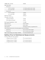
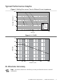
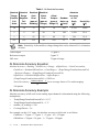
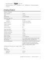
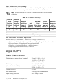
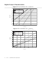
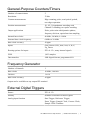
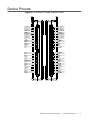
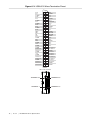
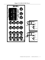
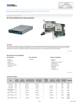
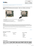
DEVICE SPECIFICATIONS
NI USB-6212
M Series Data Acquisition: 16 AI, 2 AO, 32 DIO Bus-Powered USB
The following specifications are typical at 25 °C, unless otherwise noted. For more
information about the NI USB-6212, refer to the NI USB-621x User Manual available at
ni.com/manuals.
Caution The input/output ports of this device are not protected for electromagnetic
interference due to functional reasons. As a result, this device may experience
reduced measurement accuracy or other temporary performance degradation when
connected cables are routed in an environment with radiated or conducted radio
frequency electromagnetic interference.
To ensure that this device functions within specifications in its operational electromagnetic
environment and to limit radiated emissions, care should be taken in the selection, design, and
installation of measurement probes and cables.
Analog Input
Number of channels
8 differential or 16 single ended
ADC resolution
16 bits
DNL
No missing codes guaranteed
INL
Refer to the AI Absolute Accuracy section
Sample rate
Single channel maximum
400 kS/s
Multichannel maximum (aggregate)
400 kS/s
Minimum
0 S/s
Timing resolution
50 ns
Timing accuracy
50 ppm of sample rate
Input coupling
DC
Input range
±0.2 V, ±1 V, ±5 V, ±10 V
Maximum working voltage for analog inputs
(signal + common mode)
±10.4 V of AI GND
CMRR (DC to 60 Hz)
100 dB
Input impedance
Device on
AI+ to AI GND
>10 GΩ in parallel with 100 pF
AI- to AI GND
>10 GΩ in parallel with 100 pF
Device off
AI+ to AI GND
1,200 Ω
AI- to AI GND
1,200 Ω
Input bias current
±100 pA
Crosstalk (at 100 kHz)
Adjacent channels
-75 dB
Non-adjacent channels
-90 dB
Small signal bandwidth (-3 dB)
1.5 MHz
Input FIFO size
4,095 samples
Scan list memory
4,095 entries
Data transfers
USB Signal Stream, programmed I/O
Overvoltage protection for all analog input and sense channels
Device on
±30 V for up to two AI pins
Device off
±20 V for up to two AI pins
Input current during overvoltage condition
±20 mA maximum/AI pin
Settling Time for Multichannel Measurements
Accuracy, full-scale step, all ranges
2
|
±90 ppm of step (±6 LSB)
2.5 μs convert interval
±30 ppm of step (±2 LSB)
3.5 μs convert interval
±15 ppm of step (±1 LSB)
5.5 μs convert interval
ni.com |
NI USB-6212 Device Specifications
Typical Performance Graphs
Figure 1. Settling Error versus Time for Different Source Impedances
Error (ppm of Step Size)
10 k
1k
100
<1 kΩ
2 kΩ
5 kΩ
10 kΩ
10
1
1
10
100
Time (µs)
Figure 2. AI CMRR
140
CMRR (dB)
120
100
80
60
40
60 100
1k
10 k
100 k
Frequency (Hz)
AI Absolute Accuracy
Note Accuracies listed are valid for up to one year from the device external
calibration.
NI USB-6212 Device Specifications
|
© National Instruments
|
3
Table 1. AI Absolute Accuracy
Nominal Nominal Residual Residual
Absolute
Range
Range
Gain
Offset
Offset
Accuracy
Positive Negative
Error
Error
at Full
Tempco Random
Full
Full
(ppm of (ppm of
Noise, σ
Scale
Sensitivity
(ppm of
Scale
Scale
Reading) Range) Range/°C) (μVrms)
(μV)
(μV)
10
-10
75
20
34
295
2,710
118.0
5
-5
85
20
36
149
1,420
59.6
1
-1
95
25
49
32
310
12.8
0.2
-0.2
135
40
116
13
89
5.2
Note Sensitivity is the smallest voltage change that can be detected. It is a function
of noise.
Gain tempco
7.3 ppm/°C
Reference tempco
5 ppm/°C
INL error
76 ppm of range
AI Absolute Accuracy Equation
AbsoluteAccuracy = Reading · (GainError) + Range · (OffsetError) + NoiseUncertainity
GainError = ResidualAIGainError + GainTempco · (TempChangeFromLastInternalCal)
+ ReferenceTempco · (TempChangeFromLastExternalCal)
OffsetError = ResidualAIOffsetError + OffsetTempco ·
(TempChangeFromLastInternalCal) + INLError
NoiseUncertainty =
100 points.
Random Noise ⋅ 3
for a coverage factor of 3 σ and averaging
100
AI Absolute Accuracy Example
Absolute accuracy at full scale on the analog input channels is determined using the following
assumptions:
•
TempChangeFromLastExternalCal = 10 °C
•
TempChangeFromLastInternalCal = 1 °C
•
number_of_readings = 100
•
CoverageFactor = 3 σ
For example, on the 10 V range, the absolute accuracy at full scale is as follows:
GainError = 75 ppm + 7.3 ppm · 1 + 5 ppm · 10 = 132 ppm
OffsetError = 20 ppm + 34 ppm · 1 + 76 ppm = 130 ppm
4
|
ni.com |
NI USB-6212 Device Specifications
NoiseUncertainity =
295 µ� ⋅ 3
= 88.5 µV
100
AbsoluteAccuracy = 10 V · (GainError) + 10 V · (OffsetError) + NoiseUncertainity =
2,710 µV
Analog Output
Number of channels
2
DAC resolution
16 bits
DNL
±1 LSB
Monotonicity
16 bit guaranteed
Maximum update rate
1 channel
250 kS/s
2 channels
250 kS/s per channel
Timing accuracy
50 ppm of sample rate
Timing resolution
50 ns
Output range
±10 V
Output coupling
DC
Output impedance
0.2 Ω
Output current drive
±2 mA
Overdrive protection
±30 V
Overdrive current
2.4 mA
Power-on state
±20 mV
Power-on glitch
±1 V for 200 ms
Output FIFO size
8,191 samples shared among channels used
Data transfers
USB Signal Stream, programmed I/O
AO waveform modes
Non-periodic waveform, periodic waveform
regeneration mode from onboard FIFO,
periodic waveform regeneration from host
buffer including dynamic update
Settling time, full-scale step, 15 ppm (1 LSB) 32 µs
Slew rate
5 V/µs
Glitch energy
Magnitude
100 mV
Duration
2.6 µs
NI USB-6212 Device Specifications
|
© National Instruments
|
5
AO Absolute Accuracy
Absolute accuracy at full-scale numbers is valid immediately following internal calibration
and assumes the device is operating within 10 °C of the last external calibration.
Note Accuracies listed are valid for up to one year from the device external
calibration.
Table 2. AO Absolute Accuracy
Nominal
Range
Positive
Full Scale
(V)
Nominal
Range
Negative
Full Scale
(V)
Residual
Gain Error
(ppm of
Reading)
Gain
Tempco
(ppm/°C)
Residual
Offset
Error (ppm
of Range)
Offset
Tempco
(ppm of
Range/°C)
Absolute
Accuracy
at Full
Scale (μV)
10
-10
90
11
60
12
3,512
Reference tempco
5 ppm/°C
INL error
128 ppm of range
AO Absolute Accuracy Equation
AbsoluteAccuracy = OutputValue · (GainError) + Range · (OffsetError)
GainError = ResidualGainError + GainTempco · (TempChangeFromLastInternalCal) +
ReferenceTempco · (TempChangeFromLastExternalCal)
OffsetError = ResidualOffsetError + AOOffsetTempco ·
(TempChangeFromLastInternalCal) + INLError
Digital I/O/PFI
Static Characteristics
Digital input or output (Screw Terminal)
32 total, 16 (P0.<0..15>),
16 (PFI <0..7>/P1.<0..7>,
PFI <8..15>/P2.<0..7>)
Digital input or output
(Mass Termination/BNC)
24 total, 8 (P0.<0..7>),
16 (PFI <0..7>/P1.<0..7>,
PFI <8..15>/P2.<0..7>)
Ground reference
D GND
Pull-down resistor
50 kΩ typical, 20 kΩ minimum
Input voltage protection
±20 V on up to 8 pins1
6
|
ni.com |
NI USB-6212 Device Specifications
PFI Functionality
Functionality
Static digital input, static digital output, timing
input, timing output
Timing output sources
Many AI, AO, counter timing signals
Debounce filter settings
125 ns, 6.425 µs, 2.56 ms, disable; high and
low transitions; selectable per input
Maximum Operating Conditions
IOL output low current
16 mA maximum
IOH output high current
-16 mA maximum
Digital Input Characteristics
Level
Minimum
Maximum
VIL input low voltage
0V
0.8 V
VIH input high voltage
2.2 V
5.25 V
IIL input low current (Vin = 0 V)
-
-10 μA
IIH input high current (Vin = 5 V)
-
250 μA
Positive-going threshold (VT+)
-
2.2 V
Negative-going threshold (VT-)
0.8 V
-
Delta VT hysteresis (VT+ - VT-)
0.2 V
-
1
Stresses beyond those listed under Input voltage protection may cause permanent damage to the
device.
NI USB-6212 Device Specifications |
© National Instruments
|
7
Digital Output Characteristics
Figure 3. PFI <0..15>/P0.<0..15>: Ioh versus Voh
0
55 °C; Vdd = 4.5 V
25 °C; Vdd = 5.0 V
0 °C; Vdd = 5.5 V
–5
–10
IOH (mA)
–15
–20
–25
–30
–35
–40
–45
–50
2
3
4
5
6
VOH (V)
Figure 4. PFI <0..15>/P0.<0..15>: Iol versus Vol
40
55 °C; Vdd = 4.5 V
25 °C; Vdd = 5.0 V
0 °C; Vdd = 5.5 V
35
30
Iol (mA)
25
20
15
10
5
0
0
0.2
0.4
0.6
Vol (V)
8
|
ni.com
|
NI USB-6212 Device Specifications
0.8
1
1.2
General-Purpose Counters/Timers
Number of counter/timers
2
Resolution
32 bits
Counter measurements
Edge counting, pulse, semi-period, period,
two-edge separation
Position measurements
X1, X2, X4 quadrature encoding with
Channel Z reloading; two-pulse encoding
Output applications
Pulse, pulse train with dynamic updates,
frequency division, equivalent time sampling
Internal base clocks
80 MHz, 20 MHz, 0.1 MHz
External base clock frequency
0 MHz to 20 MHz
Base clock accuracy
50 ppm
Inputs
Gate, Source, HW_Arm, Aux, A, B, Z,
Up_Down
Routing options for inputs
PFI <0..15>, many internal signals
FIFO
1,023 samples
Data transfers
USB Signal Stream, programmed I/O
Frequency Generator
Number of channels
1
Base clocks
10 MHz, 100 kHz
Divisors
1 to 16
Base clock accuracy
50 ppm
Output can be available on any output PFI terminal.
External Digital Triggers
Source
PFI <0..15>
Polarity
Software-selectable for most signals
Analog input function
Start Trigger, Reference Trigger,
Pause Trigger, Sample Clock, Convert Clock,
Sample Clock Timebase
NI USB-6212 Device Specifications
|
© National Instruments
|
9
Analog output function
Start Trigger, Pause Trigger, Sample Clock,
Sample Clock Timebase
Counter/timer function
Gate, Source, HW_Arm, Aux, A, B, Z,
Up_Down
Bus Interface
USB
USB 2.0 Hi-Speed or full-speed2
USB Signal Stream
4, can be used for analog input, analog output,
counter/timer 0, counter/timer 1
Current Limits
+5 V terminal as output3
Voltage
4.6 V to 5.2 V
Current (internally limited)
+5 V terminal as
50 mA maximum, shared with digital outputs
input3
Voltage
4.75 V to 5.35 V
Current
350 mA maximum, self-resetting fuse
Caution Do not exceed 16 mA per DIO pin.
Protection
±10 V
Power Requirements
Input voltage on USB port
4.5 V to 5.25 V in configured state
Maximum inrush current
500 mA
No load typical current
320 mA at 4.5 V
2
3
10
|
If you are using an USB M Series device in full-speed mode, device performance will be lower and
you will not be able to achieve maximum sample/update rates.
USB Screw Terminal/BNC devices have a self-resetting fuse that opens when current exceeds this
specification. USB Mass Termination devices have a user-replaceable socketed fuse that opens
when current exceeds this specification. Refer to the NI USB-621x User Manual for information
about fuse replacement.
ni.com |
NI USB-6212 Device Specifications
Maximum load
Typical current
400 mA at 4.5 V
Suspend current
260 μA typical
Physical Characteristics
Dimensions (includes connectors)
Screw terminal enclosure
16.9 cm × 9.4 cm × 3.1 cm
(6.65 in. × 3.70 in. × 1.20 in.)
Mass Termination
19.3 cm × 9.4 cm × 3.1 cm
(7.61 in. × 3.68 in. × 1.20 in.)
BNC enclosure
23.5 cm × 11.2 cm × 6.4 cm
(9.25 in. × 4.40 in. × 2.50 in.)
Weight
Screw Terminal
206 g (7.2 oz)
Mass Termination
227 g (8.0 oz)
BNC
950 g (33.5 oz)
OEM
76 g (2.6 oz)
I/O connectors
Screw terminal
4 16-position combicon
Mass Termination
1 68-pin SCSI
BNC
19 BNCs and 26 screw terminals
USB connector
Series B receptacle
Screw terminal wiring
16 to 28 AWG
Torque for screw terminals
0.22 to 0.25 N · m (2.0 to 2.2 lb · in.)
Calibration
Recommended warm-up time
15 minutes
Calibration interval
1 year
Environmental
Operating temperature
0 ºC to 45 ºC
Storage temperature
-20 ºC to 70 ºC
NI USB-6212 Device Specifications
|
© National Instruments
|
11
Humidity
10% RH to 90% RH, noncondensing
Maximum altitude
2,000 m
Pollution Degree
2
Indoor use only.
Maximum Working Voltage
Maximum working voltage refers to the signal voltage plus the common-mode voltage.
Channel-to-earth ground
11 V, Measurement Category I
Measurement Category I is for measurements performed on circuits not directly connected to
the electrical distribution system referred to as MAINS voltage. MAINS is a hazardous live
electrical supply system that powers equipment. This category is for measurements of voltages
from specially protected secondary circuits. Such voltage measurements include signal levels,
special equipment, limited-energy parts of equipment, circuits powered by regulated lowvoltage sources, and electronics.
Caution Do not use for measurements within Categories II, III, or IV.
Note Measurement Categories CAT I and CAT O (Other) are equivalent. These test
and measurement circuits are not intended for direct connection to the MAINS
building installations of Measurement Categories CAT II, CAT III, or CAT IV.
Safety
This product is designed to meet the requirements of the following electrical equipment safety
standards for measurement, control, and laboratory use:
•
IEC 61010-1, EN 61010-1
•
UL 61010-1, CSA 61010-1
Note For UL and other safety certifications, refer to the product label or the Online
Product Certification section.
Electromagnetic Compatibility
This product meets the requirements of the following EMC standards for sensitive electrical
equipment for measurement, control, and laboratory use:
•
EN 61326-2-1 (IEC 61326-2-1): Class A emissions; Basic immunity
•
EN 55011 (CISPR 11): Group 1, Class A emissions
•
AS/NZS CISPR 11: Group 1, Class A emissions
12
|
ni.com
|
NI USB-6212 Device Specifications
•
•
FCC 47 CFR Part 15B: Class A emissions
ICES-001: Class A emissions
Note In the United States (per FCC 47 CFR), Class A equipment is intended for
use in commercial, light-industrial, and heavy-industrial locations. In Europe,
Canada, Australia and New Zealand (per CISPR 11) Class A equipment is intended
for use only in heavy-industrial locations.
Note Group 1 equipment (per CISPR 11) is any industrial, scientific, or medical
equipment that does not intentionally generate radio frequency energy for the
treatment of material or inspection/analysis purposes.
Note For EMC declarations and certifications, and additional information, refer to
the Online Product Certification section.
CE Compliance
This product meets the essential requirements of applicable European Directives, as follows:
•
2014/35/EU; Low-Voltage Directive (safety)
•
2014/30/EU; Electromagnetic Compatibility Directive (EMC)
•
2011/65/EU; Restriction of Hazardous Substances (RoHS)
Online Product Certification
Refer to the product Declaration of Conformity (DoC) for additional regulatory compliance
information. To obtain product certifications and the DoC for this product, visit ni.com/
certification, search by model number or product line, and click the appropriate link in the
Certification column.
Environmental Management
NI is committed to designing and manufacturing products in an environmentally responsible
manner. NI recognizes that eliminating certain hazardous substances from our products is
beneficial to the environment and to NI customers.
For additional environmental information, refer to the Minimize Our Environmental Impact
web page at ni.com/environment. This page contains the environmental regulations and
directives with which NI complies, as well as other environmental information not included in
this document.
NI USB-6212 Device Specifications
|
© National Instruments
|
13
Waste Electrical and Electronic Equipment (WEEE)
EU Customers At the end of the product life cycle, all NI products must be
disposed of according to local laws and regulations. For more information about
how to recycle NI products in your region, visit ni.com/environment/weee.
电子信息产品污染控制管理办法(中国 RoHS)
中国客户 National Instruments 符合中国电子信息产品中限制使用某些有害物
质指令(RoHS)。关于 National Instruments 中国 RoHS 合规性信息,请登录
ni.com/environment/rohs_china。(For information about China RoHS
compliance, go to ni.com/environment/rohs_china.)
14
|
ni.com |
NI USB-6212 Device Specifications
Device Pinouts
48 47 46 45 44 43 42 41 40 39 38 37 36 35 34 33
17 18 19 20 21 22 23 24 25 26 27 28 29 30 31 32
AI 1
AI 9
AI 2
AI 10
AI 3
AI 11
AI SENSE
AI 4
AI 12
AI 5
AI 13
AI GND
AI 6
AI 14
AI 7
AI 15
1 2 3 4 5 6 7 8 9 10 11 12 13 14 15 16
PFI 0/P1.0
PFI 1/P1.1
PFI 2/P1.2
PFI 3/P1.3
D GND
PFI 4/P1.4
PFI 5/P1.5
PFI 6/P1.6
PFI 7/P1.7
+5 V
D GND
AO 0
AO 1
AO GND
AI 0
AI 8
PFI 8/P2.0
PFI 9/P2.1
PFI 10/P2.2
PFI 11/P2.3
D GND
PFI 12/P2.4
PFI 13/P2.5
PFI 14/P2.6
PFI 15/P2.7
+5 V
D GND
P0.0
P0.1
P0.2
P0.3
D GND
64 63 62 61 60 59 58 57 56 55 54 53 52 51 50 49
Figure 5. NI USB-6212 Screw Terminal Pinout
D GND
P0.4
P0.5
P0.6
P0.7
D GND
P0.8
P0.9
P0.10
P0.11
D GND
P0.12
P0.13
P0.14
P0.15
D GND
NI USB-6212 Device Specifications
|
© National Instruments
|
15
Figure 6. NI USB-6212 Mass Termination Pinout
AI 8
34 68
AI 0
AI 1
33 67
AI GND
AI GND
32 66
AI 9
AI 10
31 65
AI 2
AI 3
30 64
AI GND
AI GND
29 63
AI 4
28 62
AI SENSE
AI GND
27 61
AI 12
AI 13
26 60
AI 5
AI 6
25 59
AI GND
AI GND
24 58
AI 14
AI 15
23 57
AI 7
AO 0
22 56
AI GND
AO 1
21 55
AO GND
NC
P0.4
20 54
19 53
AO GND
D GND
D GND
18 52
P0.0
P0.1
17 51
P0.5
P0.6
16 50
D GND
D GND
15 49
P0.2
+5 V
14 48
P0.7
D GND
13 47
P0.3
D GND
12 46
PFI 11/P2.3
PFI 0/P1.0
11 45
PFI 10/P2.2
PFI 1/P1.1
10 44
D GND
D GND
9
43
PFI 2/P1.2
+5 V
8
42
PFI 3/P1.3
D GND
7
41
PFI 4/P1.4
PFI 5/P1.5
6
40
PFI 13/P2.5
PFI 6/P1.6
5
39
PFI 15/P2.7
D GND
4
38
PFI 7/P1.7
PFI 9/P2.1
3
37
PFI 8/P2.0
PFI 12/P2.4
2
36
D GND
PFI 14/P2.6
1
35
D GND
AI 11
NC = No Connect
16
|
ni.com |
TERMINAL 34
TERMINAL 68
TERMINAL 1
TERMINAL 35
NI USB-6212 Device Specifications
Figure 7. NI USB-6212 BNC Pinout
AI x +
+
–
AI x –
GS
FS
Floating
Source
0.1 µF
5 kΩ
AI GND
USB-621x Device
AI x +
+
–
AI x –
GS
FS
GroundReferenced
Source
0.1 µF
5 kΩ
AI GND
NI USB-6212/6216
USB-621x Device
NI USB-6212 Device Specifications
|
© National Instruments
|
17
Refer to the NI Trademarks and Logo Guidelines at ni.com/trademarks for information on National Instruments trademarks.
Other product and company names mentioned herein are trademarks or trade names of their respective companies. For patents
covering National Instruments products/technology, refer to the appropriate location: Help»Patents in your software, the
patents.txt file on your media, or the National Instruments Patent Notice at ni.com/patents. You can find information about
end-user license agreements (EULAs) and third-party legal notices in the readme file for your NI product. Refer to the Export
Compliance Information at ni.com/legal/export-compliance for the National Instruments global trade compliance policy and
how to obtain relevant HTS codes, ECCNs, and other import/export data. NI MAKES NO EXPRESS OR IMPLIED WARRANTIES
AS TO THE ACCURACY OF THE INFORMATION CONTAINED HEREIN AND SHALL NOT BE LIABLE FOR ANY ERRORS.
U.S. Government Customers: The data contained in this manual was developed at private expense and is subject to the
applicable limited rights and restricted data rights as set forth in FAR 52.227-14, DFAR 252.227-7014, and DFAR 252.227-7015.
© 2015 National Instruments. All rights reserved.
375196B-01
Sep15