1
Microcontroller – based directional transducer for child location
dsh
ire
UNIVERSITY OF HERTFORDSHIRE
Faculty of Engineering & Information Sciences
Un
ive
rsit
yo
fH
ert
for
BACHELOR OF ENGINEERING DEGREE WITH
HONOURS IN ELECTRICAL AND ELECTRONIC
ENGINEERING
Project Report
MICROCONTROLLER – BASED DIRECTIONAL
TRANSDUCER FOR CHILD LOCATION
Clement Yuk Leen Pang
April 2003
Un
ive
rsit
yo
fH
ert
for
dsh
ire
Microcontroller – based directional transducer for child location
Microcontroller – based directional transducer for child location
Abstract
Un
ive
rsit
yo
fH
ert
for
dsh
ire
This report covers the complete stages of designing a radio wave’s (wireless) based child locator
from an initial concept to a working printed circuit board (PCB) solution. Hardware and
software implementations have been aimed to produce a low cost portable system, in particular
the testing and evaluation of the final design is discussed in relation to the product specification
outlined in the introduction. Conclusively, the report refers to the effectiveness of the design
and issues regarding future developments.
Clement Y L Pang
i
Microcontroller – based directional transducer for child location
Acknowledgement
ire
I would like to take this opportunity to thank Stuart Archer and his team in Mitsubishi
Semiconductors for their support, help and advice.
My thanks also go to my project supervisor Kate Williams for her consistent support and
guidance throughout the project period and Tony Crook for his additional advice.
Un
ive
rsit
yo
fH
ert
for
dsh
Finally, I would like to thank all my family and friends, Scott, Mane and Jamie, especially my
parents and Cecilia who all have helped me throughout my years at Hertfordshire.
Clement Y L Pang
ii
Microcontroller – based directional transducer for child location
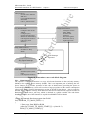
Contents
Un
ive
rsit
yo
fH
ert
for
dsh
ire
Chapter 1
Introduction.................................................................................................................................1
1.0
Chapter Overview ...............................................................................................................................1
1.1
Project aims and objectives................................................................................................................1
1.2
Design limitations...............................................................................................................................1
1.3
Initial product specification................................................................................................................2
1.4
Summary .............................................................................................................................................3
Chapter 2
Investigation and Research ........................................................................................................4
2.0
Chapter Overview ...............................................................................................................................4
2.1
Market potential ..................................................................................................................................4
2.2
Investigation in location devices........................................................................................................4
2.2.1
GPS..............................................................................................................................................4
2.2.2
Indoor location system ...............................................................................................................5
2.2.3
Radar and Sonar .........................................................................................................................5
2.3
Required RF Distance.........................................................................................................................5
2.4
Investigation and research Summary.................................................................................................5
Chapter 3
Hardware Implementation .........................................................................................................7
3.0
Chapter Overview ...............................................................................................................................7
3.1
Transmitter overview..........................................................................................................................7
3.1.1
Power supply ..............................................................................................................................7
3.1.2
Voltage reference .......................................................................................................................8
3.1.3
Serial Connector .........................................................................................................................9
3.1.4
Transmitter M16C/62N MCU ...................................................................................................9
3.1.5
Buffer ..........................................................................................................................................9
3.1.6
Transmitter unit ........................................................................................................................10
3.1.7
Antenna .....................................................................................................................................10
3.2
Receiver Overview ...........................................................................................................................11
3.2.1
Receiver unit .............................................................................................................................11
3.2.2
Power supply ............................................................................................................................12
3.2.3
LCD...........................................................................................................................................13
3.2.4
Receiver M16C/62A MCU......................................................................................................13
3.2.5
Buzzer .......................................................................................................................................13
3.2.6
Serial connector and Antenna..................................................................................................14
3.3
Additional hardware Notes ..............................................................................................................14
3.4
Hardware implementation summary ...............................................................................................14
Chapter 4
Transmitter and Receiver Printed Circuit Board....................................................................15
4.0
Chapter Overview .............................................................................................................................15
4.1
Printed Circuit Board........................................................................................................................15
4.2
PCB impediment ...............................................................................................................................17
4.3
PCB summary ...................................................................................................................................17
Chapter 5
Software Development.............................................................................................................18
5.0
Chapter Overview .............................................................................................................................18
5.1
Development Environment ..............................................................................................................18
5.1.1
C compiler.................................................................................................................................18
5.1.2
KD30 Debugger........................................................................................................................18
5.1.3
FLASH starter...........................................................................................................................18
5.2
Transmitter Source code...................................................................................................................19
5.2.1
Main function ...........................................................................................................................20
5.2.2
Tx_main Function ....................................................................................................................21
5.2.3
Diagnostic Function .................................................................................................................21
5.2.4
Sleep Mode ...............................................................................................................................22
5.2.5
INT0 Interrupt...........................................................................................................................22
5.3
Receiver Source code .......................................................................................................................22
5.3.1
Main Function...........................................................................................................................22
5.3.2
Rx_main function.....................................................................................................................22
5.3.3
Diagnostic function ..................................................................................................................22
5.3.4
Standby Function......................................................................................................................23
5.3.5
Timer A0 Interrupt Service Routine .......................................................................................24
5.3.6
5 KHz buzzer signal .................................................................................................................24
Clement Y L Pang
iii
Microcontroller – based directional transducer for child location
Un
ive
rsit
yo
fH
ert
for
dsh
ire
5.3.7
Software LCD...........................................................................................................................24
5.4
Software summary............................................................................................................................24
Chapter 6
Testing and Specification comparison phase..........................................................................26
6.0
Chapter Overview .............................................................................................................................26
6.1
Hardware modification.....................................................................................................................26
6.1.1
Tx module RESET IC ..............................................................................................................26
6.1.2
Rx buffer ...................................................................................................................................26
6.1.3
Tx and Rx Antenna ..................................................................................................................26
6.2
Specification Comparison ................................................................................................................29
6.3
System current consumption............................................................................................................29
6.3.1
Transmitter module ..................................................................................................................30
6.3.2
Receiver module.......................................................................................................................31
6.4
Battery monitoring with ADC in Diagnostic feature .....................................................................32
6.5
Transmitter and Receiver data .........................................................................................................33
6.6
RF Range and reliability...................................................................................................................35
6.7
5 & 12 KHz signal ............................................................................................................................36
6.8
Package dimensions..........................................................................................................................36
6.9
Weight ...............................................................................................................................................37
6.10 Power Supply....................................................................................................................................37
6.11 Cost Analysis ....................................................................................................................................37
6.12 Chapter Summary .............................................................................................................................37
Chapter 7 Conclusion........................................................................................................................................39
7.0
Conclusion.........................................................................................................................................39
7.1
Future Development .........................................................................................................................41
7.1.1
Software LCD...........................................................................................................................41
7.1.2
Tx and Rx MCU .......................................................................................................................42
7.1.3
Antenna Design ........................................................................................................................42
7.1.4
Data Encryption........................................................................................................................42
7.1.5 Product Durability ...........................................................................................................................42
Reference List ....................................................................................................................................................43
Bibliography ......................................................................................................................................................44
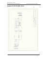
Appendix A - 1: Tx and Rx circuit diagram ....................................................................................................45
Appendix A - 2: Tx and Rx Development Board............................................................................................48
Appendix B: Component Listing and Cost......................................................................................................49
Appendix C: Software Listing..........................................................................................................................51
Transmitter XCL file: ...............................................................................................................................52
Transmitter Source Code:.........................................................................................................................55
Common header file: ................................................................................................................................63
Receiver XCL file: ....................................................................................................................................64
Receiver Source Code: .............................................................................................................................67
Common Files:..........................................................................................................................................74
Appendix D: Gantt Chart ..................................................................................................................................75
Appendix E – 1: Rx and Tx PCB layout..........................................................................................................80
Receiver PCB layout: ...............................................................................................................................81
Receiver 3V PCB layout: .........................................................................................................................82
Appendix E – 2: Rx and Tx PCB .....................................................................................................................83
Appendix F: M16C User Manual .....................................................................................................................84
Pin Configuration and block diagram of M16C/62 A and N device: ....................................................85
Performance Outline:................................................................................................................................86
Appendix G: dBm to watts conversion chart...................................................................................................87
Appendix H: MF-TEN-NINE CABLE ............................................................................................................88
Clement Y L Pang
iv
Microcontroller – based directional transducer for child location
dsh
ire
Table 1 Product Specification.............................................................................................................................2
Table 2 Product specification comparison table..............................................................................................29
Table 3 Transmitter module current consumption ..........................................................................................30
Table 4 Receiver module current consumption...............................................................................................31
Table 5 Current consumption comparisons .....................................................................................................31
Table 6 RF range and reliability results...........................................................................................................35
Table 7 Buzzer's effectiveness..........................................................................................................................36
Table 8 Dimensions comparison ......................................................................................................................36
Table 9 Weight comparison..............................................................................................................................37
Table 10 Power supply comparison .................................................................................................................37
Un
ive
rsit
yo
fH
ert
for
Figure 1 Transmitter Module block diagram.....................................................................................................7
Figure 2 Tx power supply...................................................................................................................................8
Figure 3 10 pin serial connector .........................................................................................................................9
Figure 4 Mitsubishi's M16C 3 Diamonds Board...............................................................................................9
Figure 5 Transmitter module ............................................................................................................................10
Figure 6 Receiver Module block diagram .......................................................................................................11
Figure 7 Receiver RX unit ................................................................................................................................12
Figure 8 Receiver power supply.......................................................................................................................12
Figure 9 14 segment 8 digit LCD.....................................................................................................................13
Figure 10 Tx PCB (40mm by 70mm) ..............................................................................................................15
Figure 11 Tx PCB in 3Dimensional view........................................................................................................16
Figure 12 Rx PCB (65mm by 100mm)............................................................................................................16
Figure 13 Rx PCB in 3Dimensional view .......................................................................................................16
Figure 14 Rx 3V version (45mm by 90mm) ...................................................................................................17
Figure 15 M16C software development environment ....................................................................................19
Figure 16 Transmitter source code block diagram..........................................................................................20
Figure 17 Rx software block diagram..............................................................................................................24
Figure 18 Prototype received signal.................................................................................................................27
Figure 19 PCB Track antenna signal ...............................................................................................................27
Figure 20 PCB with wire antenna signal .........................................................................................................28
Figure 21 Radiation pattern [1] ..........................................................................................................................28
Figure 22 Voltage relationship diagram ..........................................................................................................33
Figure 23 Hyper Terminal Set up.....................................................................................................................33
Figure 24 Transmitted 0xAA data....................................................................................................................34
Figure 25 Received data....................................................................................................................................34
Figure 26 5 KHz buzzer signal .........................................................................................................................36
Figure 27 Hyper Terminal message setup .......................................................................................................41
Clement Y L Pang
v
Microcontroller – based directional transducer for child location
Chapter Overview
Introduction
ire
Chapter 1
Chapter 2
dsh
“Chapter 1 defines the sole purpose of this project in correspondence to the
aims and objectives. Information regarding the product specification of the
system can be found within this section.”
Investigation and Research
Chapter 3
Hardware Implementation
for
“The essence of this chapter is to illustrate the background knowledge needed
to understand and tackle the project’s aim. It will also provide information
regarding the current technologies used in relation to object/child location. The
results from this section will conclude to the technology chosen for the child
locator.”
Transmitter and Receiver Printed Circuit Board (PCB)
fH
Chapter 4
ert
“This chapter illustrates all the different devices used for both the transmitter
(Tx) and receiver (Rx) circuit. It describes and explains why certain devices
were used and its relevance to the final design concept.”
Chapter 5
yo
“With the prototype complete, the next stage was to import the schematics of
the modules onto PCB. This chapter highlights the stages taken in order to
produce the required PCB, which was to be later encapsulated if time permitted,
to create the final product as outlined in the original aim.”
Software Development
Chapter 6
rsit
“The objectives of this chapter are to explain and describe the software code
written in ‘C’ for the transmitter and receiver MCU. It will provide a guide for
all the features implemented such as the low power features, ADC battery
monitor, signal transmission and reception. In order to appreciate the software
developed, an overview of the development environment will also be
discussed.”
Testing and specification comparison Phase
Un
ive
“Chapter 6 evaluates the full performance of the final design in relation to the
project’s aim and product specification outlined in chapter 1.”
Chapter 7
Conclusion
“Chapter 7 provides a summary of the major findings of this report and
discusses recommendations for further work and improvements that could be
implemented to the existing system.”
Clement Y L Pang
vi
Microcontroller – based directional transducer for child location
for
dsh
AM
ADC
Clk
CMOS
DC
DMM
FM
FSV
GPS
GND
I/P
LSB
IC
LCD
LED
ISR
ISI
MCU
MSB
O/P
PCB
RF
RAM
ROM
Rx
Vcc
SMD
TTL
Tx
UART
Vref
yo
fH
ert
Amplitude Modulation
Analogue to digital converter
Clock
Complimentary Metal-Oxide Semiconductor
Direct Current
Digital Multi-Meter
Frequency Modulation
Full Scale Voltage
Global Positioning System
Ground
Input
Least Significant Bit
Integrated Circuit
Liquid Crystal Display
Light Emitting Diode
Interrupt Service Routine
Inter Symbol Interference
Microcontroller Unit
Most Significant Bit
Output
Printed Circuit Board
Radio Frequency
Random Access Memory
Read Only Memory
Receiver
Supply Voltage
Surface Mount Devices
Transistor Transistor Logic
Transmitter
Universal Asynchronous Receiver Transmitter
Voltage reference
ire
Glossary of terms
Vout
Etotal
= Vin.R2 / R1+R2
= (C / ) / 4
= Estandby + Esend + Eoff
Un
ive
rsit
Equation [1] Voltage divider rule
Equation [2] ¼ wavelength antenna
Equation [3] Battery life
Clement Y L Pang
vii
Microcontroller – based
directional transducer for child location
Chapter 1
Introduction
Chapter 1 Introduction
dsh
1.0
ire
Chapter contents
1.0 Chapter Overview
1.1 Project aims and objectives
1.2 Design limitations
1.3 Product Specification
1.4 Summary
Chapter Overview
Chapter 1 defines the sole purpose of this project in correspondence to the aims and objective.
Information regarding the product specification of the system can be found within this section.
1.1
Project aims and objectives
for
The aim of this project is to design and develop a cost-effective and low power radio frequency
(RF) based child locator from initial design to a manufactured product.
fH
ert
The objective is to utilise a pair of RF modules so that the end user (adult/parent) has a
transmitter module that can send a signal to the receiver carried by the child to activate an
audible signal. The user can therefore locate the origin of the sound hence the location of the
child. To produce an efficient system, the transmitter and receiver will be controlled via a
microcontroller unit (MCU) which in turn controls the audible speaker unit and a liquid crystal
display (LCD).
With the emphasis of the project being cost-effective, low power and a complete product at the
end of the project, it has been essential to achieve a reliable RF communication link between the
transmitter and receiver unit as early into the project as possible.
1.2
Design limitations
rsit
yo
Like all portable systems the power consumption, physical size and weight must be minimal in
order to prolong the battery life and limit its overall weight. In order to overcome these issues,
the required components were preferred to be in Surface Mount Device (SMD) format, which
would largely limit the size and weight of the unit. Current consumption on the other hand was
dealt with by setting the respective MCU and other devices into their low power or shut down
modes.
With a project budget of only £50, cost limitation was the secondary restriction, which meant
precautions were taken in finding the most appropriate devices.
Un
ive
Finally the third restriction was the time limit and in order to produce a satisfactory result at the
end of this period, good time planning was essential to any project of this scale. A lot of time
was spent planning ahead, keeping to schedule and estimating any contingencies where
possible. Appendix D shows the initial Gantt chart produced compared with the actual time
spent during the project period.
Clement Y L Pang
1
Microcontroller – based
directional transducer for child location
1.3
Chapter 1
Introduction
Initial product specification
Table 1 Product Specification
PHASE 1
dsh
Specification
<5mA and <=5V power
supply
Low power Operation
<5mA and <=5V power
supply
It seems that parents or adults get concerned Min 15M and Max 25M
over their child when in or outdoors with a
separation of around 20M, therefore the
maximum range needed must balance the
requirements based on the users opinion
The pin range is large due to the fact that the 20-100Pin,
system may need additional modules listed in 8/16 bit core,
phase 2. Flash memory is preferred as it allows Flash memory
the code in the MCU to be updated (i.e. erased Low power < 30mA
and reprogrammed)
Low power Feature, i.e.
sleep mode, wait mode
Minimum of 2 timers may be used to encode < 50uA
and decode the receiving signal
Min 2 Timers
A/D channel
Used in portable equipment such as remote Standard off the shelf
controls, lighters, cameras, etc.
3/6/9V Alkaline Battery
Replacement frequency
aimed at min 6months
Typical pocket calculator size (except for the Max dimensions of
depth)
150mm*85mm*60mm
Minimal weight as the RF modules are Max of 100g
portable devices
Loud audible sound so that it can be heard Audible signal of 80dB
from a max range of 25M without any hearing
damage/impairment to the child
Used to warn the users that the unit needs a
Red flashing Light
battery replacement (important feature)
Emitting Diode (LED)
As the unit will be used in and outdoors, it Water proof, Shock
needs to withstand many of the outdoor proof, Vibration proof
weather conditions.
Temp range: 10C to 50C
Maximum budget
Max £50
PHASE 2
As many parents have more than a single child, Encode signal with
or those with many children to look after it is unique signature for
necessary to have multiple receivers to locate each unit. Hence a
each child
different audible signal
used for each child
This software based feature will be Software based solution
programmed into the MCU so that the units to self test the modules
can self diagnose themselves by running a to assure that the units
routine which test the functions of each are functioning correctly
module and its RF link
Weight
Speaker
Low battery
indicator
Un
ive
Environmental
and physical
considerations
Cost
yo
Size
rsit
Battery (power
supply)
fH
ert
MCU
Description
Low power operation
for
Features
Receiver (Rx)
module
Transmitter
(Tx) module
RF range
ire
The table below (Table 1.0) illustrates the product specification for the RF based child locator:
Multiple
modules
Diagnostic Test
Clement Y L Pang
2
Microcontroller – based
directional transducer for child location
Introduction
As the unit gets more complex, it would be 8 digit 14 segment
more user friendly for the operator to see the alphanumeric display
relevant data such as module number, (typically 36 pins)
diagnostic details, power consumption, time,
calendar, hence resulting in a more attractive
multi-purpose device
Can also be used to display a menu system for
the user to navigate through the different types
of functions
1.4
dsh
ire
LCD
Chapter 1
Summary
Un
ive
rsit
fH
Design and build a system that utilises a reliable wireless RF Link between the
transmitter and receiver.
Write source code for the microcontroller (MCU) to utilise the:
o low power features within the MCU
o shut down modes on external components i.e. transceiver ICs, Memory etc.
Buzzer circuit to produce an audible signal loud enough for the user to hear
o This section will also include software programming
Develop, build and test development board and design a Printed Circuit Board (PCB)
for the transmitter and receiver
Design box to encapsulate PCB
yo
ert
for
The aim of designing a complete child-locating device opens many doors to the available
technologies that can be used to meet the requirements set. Examing the objectives outlined, the
following report will illustrate the approaches taken in order to produce a system that will take
advantage of the current technologies. In addition, it will provide an overall understanding in
both the hardware and software implemented. The summary listed below concludes the main
objectives within this project:
Clement Y L Pang
3
Microcontroller – based
directional transducer for child location
Chapter 2
Investigation and Research
Chapter 2 Investigation and Research
dsh
2.0
ire
Chapter contents
2.0 Chapter Overview
2.1 Market potential
2.2 Investigation in location devices
2.2.1
GPS
2.2.2
Indoor location system
2.2.3
Radar and Sonar
2.3 Required RF distance
2.4 Investigation and research summary
Chapter Overview
2.1
for
The purpose of this chapter is to illustrate the background knowledge needed to understand and
tackle the project’s aim. It will also provide information regarding the current technologies used
in relation to object/child location. The results from this section will conclude to the technology
chosen for the child locator.
Market potential
fH
ert
The importance of a child’s location has become a major concern for many parents over the past
few years, with reports showing that between 700 – 800 children go missing every month in the
US alone. In order to protect children and help parents or guardians know their whereabouts,
many manufacturers are developing wristwatches and pager-sized units that can be used to track
lost individuals to within a few feet. Reports also claim that one company intends to unveil a
working prototype of an encapsulated Global Positioning System (GPS) device that could be
surgically implanted inside a person’s arm. It is also estimated that by 2006 the potential market
for child detectors will be around $200 billion USD from the president of Wherify Wireless Inc.
Investigation in location devices
rsit
2.2
yo
“The Wherify Personal Location System includes a wristwatch-sized device that combines
SiRF's SiRFstarII GPS technology, along with LSI Logic's Code Division Multiple Access
(CDMA) technology, which allows device communication through a national PCS network. As a
result, subscribers of the Personal Location System will be able to quickly determine, via a 24x7
location service center accessed through the Internet or by any phone, the location of their
children, elderly parents or other at-risk loved ones wearing the device.”[1]
To achieve the knowledge necessary to tackle the project aim, a large scale of time was spent
researching into the available location devices in the current market place.
Un
ive
2.2.1 GPS
Many current manufacturers have implemented GPS technology due to their major advantages
such as its high efficiency to work under any weather conditions, precision for object location
anywhere in the world, its 24 hours a day service with no subscription fees or set up charges.
“The Global Positioning System (GPS) is actually a constellation of 27 Earth-orbiting satellites
(24 in operation and three extras in case one fails). The U.S. military developed and
implemented this satellite network as a military navigation system, but soon opened it up to
everybody else. Each of these 3,000- to 4,000-pound solar-powered satellites circles the globe
at about 12,000 miles (19,300 km), making two complete rotations every day. The orbits are
arranged so that at any time, anywhere on Earth, there are at least four satellites "visible" in
the sky. A GPS receiver's job is to locate four or more of these satellites, figure out the distance
to each, and use this information to deduce its own location. This operation is based on a simple
mathematical principle called trilateration.”[2]
Clement Y L Pang
4
Microcontroller – based
directional transducer for child location
Chapter 2
Investigation and Research
Some of the reasons for this and other problems are listed as follows:
o
dsh
o
Signal multipath: This occurs when the GPS signal is reflected off objects such as tall
buildings or large rock surfaces before it reaches the receiver. This increases the travel
time of the signal, thereby causing errors.
Visible satellites: The more satellites a GPS receiver can "see," the better the accuracy.
Buildings, terrain, electronic interference, or sometimes even dense foliage can block
signal reception, causing position errors or possibly no position reading at all.
Therefore GPS units typically will not work indoors, underwater or underground.
Satellite geometry/shading: This refers to the relative position of the satellites at any
given time. Ideal satellite geometry exists when the satellites are located at wide angles
relative to each other. Poor geometry results when the satellites are located in a line or
in a tight grouping.
for
o
ire
Unfortunately, like many other devices on the market, some system solutions come with a
single or multiple flaws. Studying the GPS system further shows that it is difficult for the
receiver to receive any signals when operating indoors.
fH
ert
2.2.2 Indoor location system
The first indoor location sensing system was the Active Badges developed by AT&T
Cambridge. This system consisted of an infrared beacon worn by every person that was used to
emit a globally unique identifier every 10seconds. The signal is received by an IR receiver,
which in turn transmits the data to a central server where the information is converted into
useful data. Therefore this solution is purely for indoor purposes only.
Required RF Distance
rsit
2.3
yo
2.2.3 Radar and Sonar
Other wireless solutions for object location include Radar and Sonar. These solutions are not
appropriate for detecting the location of a child as Radar is unable to detect the exact location of
an object but only its radial speed factor, hence its commercial use is in motorway speed
cameras. Sonar on the other hand is mainly used to detect objects underwater, such as
submarines, vessels etc. Sonar works by sending sound energy through a medium, i.e. water,
and if an object is detected the signal is then reflected back to the transducer, hence providing
the range information through additional calculations.
Un
ive
The maximum distance that a pair of RF modules can communicate is different from product to
product. In order to choose the most appropriate distance a simple survey was carried out
regarding the distance the parent and child was apart before they would become concern about
their child. The results were some what expected with the range around 15 to 30meters+.
Knowing that the receiver system was to utilise a buzzer as the core signal for the parent to
locate, it was sensible to limit the distance for communication to the boundaries between 10m
(min) to 25m (max).
2.4
Investigation and research Summary
The main aim of this project is to build and design a system to detect the location of a child,
while keeping the cost and power consumption to a minimum. This would have been achieved
by utilising a low power microprocessor and a form of wireless communication. Knowing that
the GPS receivers are extremely precise in outdoor locations while RF communications are
efficient indoors, it would be sensible to integrate both systems into one. Unfortunately, GPS
receivers are extremely expensive, usually around the price range of £63; therefore it would
defy the objective of being low cost. Consequently a singular simplex (one way
communication) RF solution was implemented.
Clement Y L Pang
5
Microcontroller – based
directional transducer for child location
Chapter 2
Investigation and Research
Un
ive
rsit
yo
fH
ert
for
dsh
ire
The modulation scheme for the RF communication was chosen to be amplitude modulation
(AM) and not frequency modulation (FM). The reason for this is because AM has the
advantages of being low cost, readily available and AM receivers are simple to tune. Even
though their main disadvantage is in its efficiency and its vulnerability to noise, its advantages
out weigh the disadvantages, which can be improved in software within this application, hence
suiting the requirements for this project.
Clement Y L Pang
6
Microcontroller – based
directional transducer for child location
Chapter 3
Hardware Implementation
3.0
dsh
for
ert
Chapter Contents
3.0 Chapter Overview
3.1 Transmitter Overview
3.1.1
Power supply
3.1.2
Voltage Reference
3.1.3
Serial Connector
3.1.4
Transmitter M16C/62N MCU
3.1.5
Buffer
3.1.6
Transmitter unit
3.1.7
Antenna
3.2 Receiver Overview
3.2.1
Receiver unit
3.2.2
Power supply
3.2.3
LCD
3.2.4
Receiver M16C/62A MCU
3.2.5
Buzzer
3.2.6
Serial Connector and Antenna
3.3 Additional Hardware notes
3.4 Hardware Implementation summary
ire
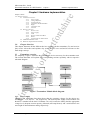
Chapter 3 Hardware Implementation
Chapter Overview
3.1
Transmitter overview
fH
This chapter illustrates all the different devices used for both the transmitter (Tx) and receiver
(Rx) circuit. It describes and explains why certain devices were used and its relevance to the
final design concept.
yo
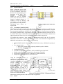
For simplicity, Figure 1 illustrates the fundamental devices necessary for the transmitter unit.
The sections thereafter will explain each corresponding sections separately with its respective
schematic diagram.
rsit
Power
Un
ive
Voltage
reference
Serial
Connector
Antenna
Transmitter
MCU
Buffer
Figure 1 Transmitter Module block diagram
3.1.1 Power supply
The MCU and transmitter data sheet shows that the operating voltages for the devices are
around 2.4V – 3.6V and 2V – 14V respectively. The chosen power supply for this module was
therefore a standard off the shelf 3V lithium coin cell, because the battery had the appropriate
voltage level, adequate current capacity (280mAh (mili amps hours)) and a small surface area
and weight of 24mm diameter and 4g respectively.
Clement Y L Pang
7
Microcontroller – based
directional transducer for child location
Chapter 3
Hardware Implementation
ert
for
dsh
ire
Having a 3V-battery supply would also eliminate the need of a 3V/3.3V regulator hence
reducing the overall cost and power consumption. For safety precautions a standard schottky
diode was used in series with the supply voltage (Vcc) to protect the on board devices in case
the battery was positioned incorrectly. As with all portable units, SW1 provides a simple means
to switch the module on or off as shown on figure 2 below.
Figure 2 Tx power supply
yo
fH
3.1.2 Voltage reference
An important feature listed in the product specification (please refer to table 1) was a low
battery indicator. In order to achieve this, the Analogue to Digital Converters (ADCs) on the
MCU was used, without a regulator for the unit, there would be no constant reference voltage
(Vref) for the ADC on the MCU therefore the onboard ADC would not be able to operate. To
compensate, a 2.5V voltage reference device U8 was used for Vref. This solution has its
advantages over using a voltage regulator as it only requires 1mA to provide a constant voltage
that can be controlled on or off by the MCU pin “high” or “low” respectively, hence obtaining
better power efficiency. More information regarding the ADC can be found in chapter 5 in the
software section.
rsit
Figure 2 shows a simple voltage divider across the supply rail (Vcc) and ground (GND). The
reason for this is so that the ADC monitoring port (Port10.0) has approximately the same
voltage level of Vref where it is used to monitor the status of the battery. Below shows the
calculations necessary in order to achieve ~2.5V supply to P10.0:
Un
ive
Using the voltage divider equation:
Equation [1]
Vout
= Vin.R2 / R1+R2
Implies that:
2.5V
R1
R1
= (3 * 1000)/R1+1000
= (3000 – 2500)/2.5
= 200Ω
Therefore
Vout = 2.5V
Vin
= 3V
Assume R2
= 1K
Hence the preferred value of 220Ω for R1 was used to supply P10.0 with 2.56V.
Clement Y L Pang
8
Microcontroller – based
directional transducer for child location
3.1.3
Chapter 3
Hardware Implementation
Serial Connector
dsh
ire
Figure 3 illustrated on the right
shows the 10-pin connector used
on the development board and
PCB to allow programming and
debugging of the MCU. This
hardware
implementation
enables the user to FLASH
(write) new code into the MCU
memory if updated software is
available, as well as allowing
connectivity to the PC’s RS232
port (COM port) using the MFTEN-NINE cable shown in
Appendix H.
for
Figure 3 10 pin serial connector
fH
ert
3.1.4 Transmitter M16C/62N MCU
The MCU used for the Tx module is the M16C/62N, Mitsubishi’s compact, cost effective low
power 16bit MCU that provides high speed processing with RISC like performance. Targeted
for many modern applications, it features low operating voltage (3.3V typical), noise immunity,
rich on-chip peripherals and C programming efficiency. Additional hardware functions such as
its 8/10bit ADC, three UART (Universal Asynchronous Receiver Transmitter) channels and
eight programmable Timers are also available hence, it was ideal for the project.
To minimise the amount of time required to implement the MCU onto the Tx module,
Mitsubishi’s M16C/62N’s 3 Diamond board was used. This is an evaluation board produced by
Mitsubishi semiconductors, which consists of the following:
yo
M30624FGNFP (M16C/62N): On-chip 265kB Flash memory, 20kB RAM operating at
5V
Two external clocks:
o Main clock speed at 2MHz (replacing standard crystal of 16MHz)
o Sub clock speed at 32768Hz
8 independent LEDs
4 Switches connected to INT0, INT1, INT2 and RESET port of the M16C
Header connectors to allow connection to all port pins of the MCU
9 Pin D-type serial socket for PC connection via UART transceiver
Simple PP3 battery connectors to power the board
rsit
Un
ive
Using the 3 Diamonds board as a
target board for evaluating the MCU
allowed the software written to be
compiled, debugged and stepped
through. Utilising the available
header connectors, allowed the
development board to be easily
linked together with external
devices providing a means of a
simple in circuit emulator where the
circuit could be tested. Figure 4
shows a simplified diagram of the
M16C/62N 3 Diamonds Board.
Figure 4 Mitsubishi's M16C 3 Diamonds Board
Information regarding the MCU and can be found in Appendix F.
3.1.5 Buffer
Clement Y L Pang
9
Microcontroller – based
directional transducer for child location
Chapter 3
Hardware Implementation
ire
The 74HC buffer, U4C as illustrated below, is a standard off the shelf component with six
internal NOT gates. The purpose for the buffer is to clean the signal from the MCU transmit pin
before reaching the transmitter and antenna. It also provides a means of isolation between the
MCU and transmitter, in case of any spurious errors that may occur.
Un
ive
rsit
yo
fH
ert
for
dsh
Figure 5 shows how the buffer is connected to the MCU pin P0.1 via the PNP transistor’s base
(B). The reason for this is to ensure that the buffer is not directly connected to the supply
voltage Vcc hence acting as an open circuit (i.e. no current flow). Once the corresponding port
pin goes “low” hence “0”, the PNP transmitter switches enabling a direct connection between
the emitter (E) and collector (C), hence linking Vcc and pin 14 of the buffer (supply voltage pin)
together. This switching method is used so that the operation of the buffer is solely dependent
on the code/port pin, therefore providing a means of controlling the buffer’s on and off time,
resulting in better power efficiency. It can be seen that this technique is also used with the
transmitter module U2.
Figure 5 Transmitter module
3.1.6 Transmitter unit
The transmitter unit AM-RT4-433 is a standard off the shelf module from RF Solutions,
illustrated in figure 5 as U2. The Tx unit features a wide operating voltage (2-14V), low current
consumption of typically 4mA with CMOS (complimentary metal-oxide semiconductor)/TTL
(transistor transistor logic) inputs, therefore this hybrid AM transmitter unit provides a complete
RF transmitter that can be utilised to transmit data at up to 4KHz directly from the MCU. Its
standard 4-pin package, provides a very simple integration to the Tx module and helps minimise
the overall size and weight.
3.1.7
Antenna
Clement Y L Pang
10
Microcontroller – based
directional transducer for child location
Chapter 3
Hardware Implementation
ire
“There seems to be little information on compact antenna design for the low power wireless
field. Good antenna design is required to realize good range performance. A good antenna
requires it to be the right type for the application. It also must be matched and tuned to the
transmitter and receiver. To get the best results, a designer should have an idea about how the
antenna works, and what the important design considerations are.”[3]
dsh
To reduce the overall size of the length of the antenna and keep an adequate performance level,
the system antenna was made by creating a track on the PCB, whilst preserving the
performance, by calculating the length of the track using equation [2] below:
Equation [2]: = (C / ) / 4
= (30000/433.9)/4
= 69.14/4
= 17.3cm = 173mm
for
where C =30000cm/s
= 433.9Hz
measured in cm
Receiver Overview
fH
3.2
ert
It would be very difficult to produce a single straight track on the PCB while trying to minimise
the module’s size, therefore the antenna was placed on the PCB more like a spiral as shown in
chapter 4 in figure 10. To improve the efficiency of the aerial it needs to radiate above a copper
based ground plane therefore a PCB fill was used in parallel as shown in figure 11.
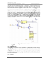
Buffer
Power
LCD
MCU
rsit
Receiver
yo
Antenna
Serial
Connector
Figure 6 Receiver Module block diagram
Un
ive
3.2.1 Receiver unit
Figure 6 shows the key devices implemented in the receiver unit. The receiver implemented in
the project is RF solutions AM-HRR3-433, U4 as shown in figure 7. Similar to that of the
transmitter, the receiver has many features suitable for the project’s specification such as its
CMOS/TTL output, low power consumption and single supply voltage. Originally, the AMHRR8-433 3V receiver was chosen for this application due to its 3V supply voltage and low
current consumption (0.5mA), but unfortunately due to availability and order quantity issues it
was unable to be obtained. Therefore AM-HRR3-433, the 5V version was chosen instead.
However the design of the receiver module will be able to support the 3V version due to its
main advantages described and the beneficial fact that both devices are pin compatible. Ideally
if production was to proceed, then the 3V device will be implemented.
The buffer U11 is connected to the receiver unit in the same fashion as it was with the
transmitter unit, hence providing the same technique for controlling the receiver’s on and off
status.
Clement Y L Pang
11
Chapter 3
Hardware Implementation
ert
for
dsh
ire
Microcontroller – based
directional transducer for child location
Figure 7 Receiver RX unit
fH
3.2.2 Power supply
The receiver unit requires typically 5V to operate; therefore a standard 9V PP3 battery was used
as the main power source. To achieve a reliable and constant supply to the system a 5V
regulator LE50CZ was used, U2 in figure 8. Unlike the transmitter module, it was necessary to
incorporate this voltage regulator so that the supply voltage for the devices was regulated down
to their appropriate operating voltage level.
Therefore
Vout
5V
R1
R1
= Vin.R2 / R1+R2
= (9 * 10000)/R1+10000
= (90000 – 50000)/5
= 8000Ω or 8KΩ
rsit
Equation [1]
Implies that:
yo
A 9V supply or a regulated 5V supply to the ADC monitoring channel of the MCU would not
allow the MCU to calculate a low battery indication as a 9V supply would damage the MCU
and 5V constant voltage would produce no change in the analogue voltage. Consequently a
simple voltage divider was used, which is the same technique implemented for the transmitter.
If we use equation [1] again for this application we get:
Vout = 5V
Vin
= 9V
Assume
R2
= 10K
Un
ive
Hence the available value of 8K2Ω for R1 was used to supply P10.0 with 4.96V.
Figure 8 Receiver power supply
Clement Y L Pang
12
Microcontroller – based
directional transducer for child location
Chapter 3
Hardware Implementation
The LCD was originally planned to display the following:
for
Menu
Time
Date/Calendar
Variable Message
rsit
yo
fH
ert
dsh
ire
3.2.3 LCD
The 36-pin LCD used on the receiver is a 14 segment 8-digit star burst display, which means
that it can easily display both numbers and alphabets. The display is also ¼ multiplexed with
four common lines to control each segment. The LCD is purely driven in software with no
external drivers but only requires two resistors per common line, shown in figure 9. By using
the software driven LCD, it would reduce the overall cost as no hardware drivers are needed and
would therefore reduce the current consumption.
Figure 9 14 segment 8 digit LCD
Un
ive
3.2.4 Receiver M16C/62A MCU
The MCU used for the receiver module is the M16C/62A, another one of Mitsubishi’s M16C 3
Diamonds Board family device. Similar to that of the M16C/62N described in section 3.1.4, the
M16C/62A consists of the same rich features in the same 100pin package. The reason for using
this device is purely due to its similar operating voltage as that of the receiver, i.e. 5V. If the
receiver unit was the original recommended 3V version, AM-HRR8-433, then the M16C/62N
would have been utilised. The advantage of using the M16C/62A in this design is because it is
also pin-compatible with the M16C/62N hence both the 3V devices (AM-HRR8-433 and
M16C/62N) can be designed into this application with minimal modifications.
3.2.5 Buzzer
The buzzer chosen to produce the audible signal for the user to trace is a simple 5V operated
piezo transducer that is activated by producing a single train of pulses i.e. square waves across
the corresponding pins.
Clement Y L Pang
13
Microcontroller – based
directional transducer for child location
Chapter 3
Hardware Implementation
3.3
ire
3.2.6 Serial connector and Antenna
The serial connector and antenna used in the receiver circuit is a replica of the one described on
the transmitter in sections 3.1.3 and 3.1.7 respectively.
Additional hardware Notes
3.4
dsh
Note that not all of the components shown within this chapter are described in detail, as they
may have been taken from recommended application circuits provided by the original
manufacturers. Appendix B shows a complete table listing all the components used with the
overall cost while Appendix A-2 shows a picture of the developed development board.
Hardware implementation summary
ert
for
Many of the devices chosen for the project suited the original requirements that were necessary
to meet the aims. Since many of the devices had no shut down pins to help reduce the overall
current consumption, additional components and techniques were used to produce the same
effect. Due to availability issues regarding the 3V receiver unit, a 5V version was opted for the
development of the receiver module. This in turn resulted in utilising the M16C/62A device for
the 5V operated receiver module.
Un
ive
rsit
yo
fH
The hardware of both Tx and Rx modules has been kept to the minimal so that it would reduce
the overall cost and weight of the modules. In order for the system to provide more
functionality, software solutions were opted, as this would have no bearing on the overall
hardware cost.
Clement Y L Pang
14
Microcontroller – based
directional transducer for child location
Chapter 5
Software Development
ire
Chapter 4 Transmitter and Receiver Printed Circuit Board
4.0
dsh
Chapter contents
4.0 Chapter Overview
4.1 Printed Circuit Board
4.2 PCB impediment
4.3 PCB summary
Chapter Overview
4.1
for
With the prototype complete, the next stage was to import the schematics of the modules onto
PCB. This chapter highlights the stages taken in order to produce the required PCB, which was
to be later encapsulated if time permitted, to create the final product as outlined in the original
aim.
Printed Circuit Board
ert
From information provided in Chapter 3, Appendix A - 1 shows the complete schematics for the
transmitter and receiver circuit produced on Protel99 SE. One of Protel’s powerful features is
that it can transfer any complete schematics onto a PCB document provided that all the
footprints for the components are present. Once the schematics were complete, footprints for
each device were added with their respective electrical characteristics.
Un
ive
rsit
yo
fH
In order to minimise the overall layout of the transmitter and receiver module, SMD
components were mainly used and situated on the bottom layer of the PCB. This proved
successful as a space saving option as it allowed through-hole components to dominate the top
layer. Regarding the 3 Diamonds board, only the MCU was taken for the final PCB design, as
the other components were not necessary. The PCB layout for both the transmitter and receiver
are shown on figure 10 and 11 and figure 12 and 13 respectively.
Figure 10 Tx PCB (40mm by 70mm)
Note: The red lines displayed on the PCB illustrate the connection lines on the top layer
whereas the blue lines are that of the bottom layer. The yellow boundaries show the component
locations.
Clement Y L Pang
15
Microcontroller – based
directional transducer for child location
Chapter 5
Software Development
dsh
ire
Note: This 3 Dimensional
view of the transmitter board
clearly illustrates the main
SMD components placed on
the bottom layer of the PCB.
The plain rectangular copper
fill located near the bottom
right of the PCB is the
copper ground plane needed
for the aerial (red spiral like
track on figure 10) to radiate.
yo
fH
ert
for
Figure 11 Tx PCB in 3Dimensional view
rsit
Figure 12 Rx PCB (65mm by 100mm)
Un
ive
Note: The dimensions of the receiver board are larger than that of the transmitter due to the
physical size of the PP3 battery and LCD display.
Figure 13 Rx PCB in 3Dimensional view
Clement Y L Pang
16
Microcontroller – based
directional transducer for child location
Chapter 5
Software Development
ert
for
dsh
ire
Note: As mentioned in chapter 3, the aerial of the receiver is similar to that of the transmitter
with its respective ground copper plane parallel to it.
If we considered using the original 3V receiver and the 3V lithium battery coin cell, then the
dimensional size would be reduced dramatically as shown in figure 14.
fH
Figure 14 Rx 3V version (45mm by 90mm)
Note: Again the same principle is used with the SMD components on the bottom layer and
through-hole devices on the top layer.
4.2
PCB impediment
rsit
yo
A great deal of time was spent on the PCB design and the positions of each component to
achieve the desired dimensions and layout. Majority of the delay came from the antenna track
section, as it had to be independent and isolated from other local links. This was finally
achieved by applying a rectangular fill over the existing aerial track during the “autoroute”
progress used by Protel to link all the different nets together. Once complete, the fill was
removed to produce the results as shown. It should also be noted that the ground plane and
aerial track links should be minimal as the links would still act as the radiating ground and
aerial, therefore the links for the ground plane and aerial was linked together manually.
Un
ive
Measurements for majority of the component’s footprints were recorded and drawn in Protel, as
the standard libraries provided did not contain them. Once the PCBs were complete with no
errors on the “design rules check” in Protel, they were printed out and physically checked with
the external components to make sure each component matched. When all the components were
checked, the PCB file was sent to a third party to be manufactured (www.pcb
www.pcb-pool.com).
4.3
PCB summary
The process of converting the complete transmitter and receiver circuit schematic to the printed
circuit board in Protel is reasonably straight forward. In practice though, a lot of time was
consumed in ensuring that all the components and layout was correct to the specification and
external devices.
Clement Y L Pang
17
Microcontroller – based
directional transducer for child location
Chapter 5
Software Development
dsh
ert
for
Chapter contents
5.0 Chapter Overview
5.1 Development Environment
5.1.1
C compiler
5.1.2
KD30 Debugger
5.1.3
FLASH starter
5.2 Transmitter Source code
5.2.1
Main function
5.2.2
Tx main function
5.2.3
Diagnostic function
5.2.4
Sleep mode
5.2.5
INT0 Interrupt
5.3 Receiver Source code
5.3.1
Main function
5.3.2
Rx_main function
5.3.3
Diagnostic function
5.3.4
Standby function
5.3.5
Timer A0 Interrupt Service routine
5.3.6
5 & 12 KHz buzzer signal
5.3.7
Software LCD
5.3.8
Software summary
ire
Chapter 5 Software Development
5.0
Chapter Overview
5.1
Development Environment
fH
The objectives of this chapter are to explain and describe the software code written in ‘C’ for
the transmitter and receiver MCU. It will provide a guide for all the features implemented such
as the low power features, ADC battery monitor, signal transmission and reception. In order to
appreciate the software developed, an overview of the development environment will also be
discussed. Full code listing can be found in Appendix C.
rsit
yo
It has been known that as the structure of a program code increases in the conventional
assembly language, the more difficult it is for programmers to comprehend. This is why
increasing amounts of embedded applications are now written in the C language. To help
develop the software for this project, a full range of development tools including compilers and
debuggers were used. Figure 15 illustrates the development environment utilised to compile,
debug and test the code.
Un
ive
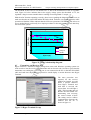
5.1.1 C compiler
The C language efficient compiler used within the Windows environment is IAR Systems Ltd
Embedded Workbench, also known as EWM16C. The full source code and program is designed
and implemented within EWM16C, where it is also compiled and edited to produce the object
file. These files are then linked with the required libraries to produce either the mot file used to
program into the target or the ieee file used for the KD30 debugger.
Libraries such as “Chip_3062x”, “iom16c62.h”, “intrm16c.h” are all specific files included in
the compiler that allows various functions, ports and interrupts to be configured and called. The
header file “common_FLASHOFF.h”, is an additional file created with all the common and
global variables and functions declared. The linker file is also a modified version of the original
to allow full RAM operation support as discussed below. For more information regarding these
files, please refer to Appendix C.
5.1.2 KD30 Debugger
The next stage after completing the software code is to test and debug the program. KD30 is
another Windows based program that allows users to step through the code, place software
break points and view information such as memory addresses, C variable information and the
program counter.
5.1.3 FLASH starter
Clement Y L Pang
18
Microcontroller – based
directional transducer for child location
Chapter 5
Software Development
ire
This program takes the mot file produced by the compiler and serially programs or flashes the
code into the target MCU, hence the software written allows the program to be fully tested on
the development prototype and PCB.
C source files
for
C Compiler
dsh
Editor
ert
Assembler
Linker
fH
Object File
rsit
Flash Starter
software
yo
MOT file / IEEE file
PC
KD30
Debugger
MCU (3 Diamonds
board)
TARGET
Un
ive
Figure 15 M16C software development environment
5.2
Transmitter Source code
To help understand the transmitter’s software operation, a block diagram, figure 16, shown on
the following page illustrates each independent function and interrupt service routine (ISR) used
in relation to the main function “main ( )”.
Clement Y L Pang
19
Microcontroller – based
directional transducer for child location
Chapter 5
Software Development
dsh
ire
Main Function:
- Provide vector table for
ISR used
- Copy all ROM functions
into RAM
- Call Tx_main function
Diagnostic Function:
- Configure clock to
main: 2MHz
- Perform ADC
operation
- Test value against
threshold (<0xF7)
- Light LED if true
Sleep Mode Function:
- Set MCU to “Stop
Mode”
fH
ert
for
Tx_main Function:
- Configure clock to sub:
32KHz
- Configure ports,
registers and interrupts
- Disable FLASH memory
- Call diagnostic function
- Call sleep_mode
function
INT0 Interrupt
requested
yo
Key Input Interrupt
rsit
INT0 ISR:
- Send data (0xAA) three
times
- Call diagnostic function
Figure 16 Transmitter source code block diagram
Un
ive
5.2.1 Main function
The objective of the main function is to copy all relevant functions in the read only memory
(ROM) to the random access memory (RAM). This is an important part of utilising the low
power features as it provides operation of the code in RAM, hence providing the option to
switch the FLASH memory circuit off to reduce a large proportion of the current consumption
(please refer to the electrical characteristic section in the MCU data sheet). Also in order for
selected ISRs to operate correctly, their addresses must also be allocated in a specific location in
RAM known as the intvec_tab array, which is declared as a global variable. The code below
demonstrates how one of the functions is copied from ROM/FLASH to RAM:
// Copy the transmit function program into RAM
for(i=0;i<RAM_TX_MAIN_SIZE;i++)
{
// Start copy from ROM to RAM
((char far *) RAM_TX_MAIN_START)[i] = ((char far *)
ROM_TX_MAIN_START)[i];
Clement Y L Pang
20
Microcontroller – based
directional transducer for child location
Chapter 5
Software Development
}
ire
Once all functions are copied, the function tx_main in RAM is called where all operation from
there onwards is solely in RAM.
dsh
5.2.2 Tx_main Function
At the beginning of this function, the software code written configures the clock operation
circuit so that the main clock is switched off and all operations work under the 32 KHz sub
clock, which enables the current consumption to be reduced further. Now that all the functions
are copied into Ram, the next stage is to switch the FLASH circuit supply off using register
“FMR0”. Port P0 through to port P10 are then configured as either input (I/P) or output (O/P)
respectively, with all the ports configured, the interrupts, UART and ADC registers are then set
to the required configurations.
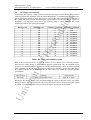
When VCC = 2.5V
Vref
Vdivider
Vdiode drop
Recommended digital
threshold in decimal:
rsit
Therefore the
digital threshold is:
= 2.2V
= 1.9V
= 0.22V
= 2.2/28
= ~10mV
yo
Each digital value:
fH
ert
for
5.2.3 Diagnostic Function
The function diagnostic ( ) is then called before the sleep_mode ( ) function that is located in a
forever loop. In order to achieve an ADC threshold to produce the low battery indication
required the value of 2.5V was chosen. This threshold voltage was chosen since the minimum
voltage required for the MCU to operate is 2.0V (more details regarding this value can be found
in Chapter 6.9). If the operating voltage of the supply falls below 2.5V the transmit module
would still have adequate time before the module switches off, hence with a threshold voltage
of 2.5V we can convert the analogue threshold into a digital hex value for the MCU to detect.
The following calculations show how the values are calculated using an 8bit (28) resolution
ADC.
= 2.2 – (1.9 + 0.22)/10*10-3
= 0.08/10*10-3
=8
= 255 – 8
= 247 = 0xF7
Un
ive
//----------------------------------------------------------------------------------------// Use ADC to measure battery status
//----------------------------------------------------------------------------------------ADCON1.5 = 1;
// Vref connected
for (pause=0xF;pause!=0;pause--); // Allow software pause for ~1us
ADCON0.6 = 1;
// Start ADC conversion now
while(ADCON0.6 != 1);
// Poll for ADC to finish
tempvalue = AD0L;
// Store value into local variable
if(tempvalue < 0xF7)
{
low_battery = ON;
// Check if below threshold
P2.0 = 1;
}
else
{
low_battery = OFF;
P2.0 = 0;
Clement Y L Pang
21
Microcontroller – based
directional transducer for child location
}
ADCON1.5 = 0;
Chapter 5
Software Development
ire
// Vref disconnected
dsh
In order for the ADC to operate it requires the main clock, therefore at the beginning of this
function the main clock is resumed and switched off again at the end. This function also
provides a test by a LED blinking on the board to indicate to the user that the LED is also
working.
for
5.2.4 Sleep Mode
The sleep mode function is a very simple function that sets the MCU to stop mode by writing to
the register “CM1”. As the MCU is set into stop mode the FLASH memory is automatically
switched off and on once it has “woken”. FLASH memory is switched on just before it enters
stop mode and off again once it returns.
Stop mode is utilised to produce minimal current consumption as the MCU alone only draws
~1A at this state.
5.3
Receiver Source code
fH
ert
5.2.5 INT0 Interrupt
INT0 interrupt is configured as an external interrupt or switch press. Hence this interrupt is only
called when the user presses the switch. Once called, the main clock is resumed and the
RS232/serial data value (0xAA in hexadecimal) is sent three times. The software then checks if
the button is still down and the LED creates a blinking effect. Upon release, the main clock is
again switched off and the diagnostic function as called to check the battery status (please refer
to section 5.2.3). Once complete and returned to the INT0 function, the code returns to the sleep
mode function awaiting the next button press to occur.
yo
To help comprehend the code written for the receiver module the following block diagram,
figure 17 illustrates the full operation of the functions described below.
rsit
5.3.1 Main Function
Similar to the main function of the transmitter, this main function also copies all the ROM
functions into RAM including the interrupt vector table. Once complete, it calls the receiver
main function located in RAM.
Un
ive
5.3.2 Rx_main function
The operations within this function are again similar to that of the transmitter where all the
relevant ports, ISR are set and configured. The main difference between the receiver and
transitter source code is the additional timer “TA1” used to call the buzzer function.
5.3.3 Diagnostic function
The purpose of this function is to detect the analogue voltage and to determine whether the
battery status is classified as low by comparing it to a predefined value as calculated below:
When VCC = 7V
Each digital value:
Recommended digital
threshold in decimal:
Therefore the
digital threshold is:
Clement Y L Pang
Vreg
Vdivider
= 4.96V
= 3.83V
= 4.96/28
= ~19mV
= 4.96 – (3.83 + 0.25)/20*10-3
= 0.88/19*10-3
= ~47
= 255 – 47
22
Microcontroller – based
directional transducer for child location
Chapter 5
Software Development
ire
= 208 = 0xD0
for
dsh
5.3.4 Standby Function
The standby function is similar to that of the sleep mode function used in the transmitter source
code. Instead of setting the MCU into stop mode, this function sets it into wait mode, since the
ISR used to wake the MCU up and check the signal does not have a high enough priority in
order to wake the MCU from stop mode. The FLASH memory is again switched on prior to
entering wait mode as the FLASH memory is automatically switched off once the MCU enters
either wait or stop mode.
fH
Diagnostic Function:
- Perform ADC
operation
- Test value against
threshold (<0xD0)
- Light LED if true
yo
Rx_main Function:
- Configure clock to main
clk/8 = 250KHz
- Configure ports,
registers and interrupts
- Disable FLASH memory
- Call Diagnostic function
- Call standby function
ert
Main Function:
- Provide vector table for
ISR used
- Copy all ROM functions
into RAM
- Call Rx_main function
rsit
Standby Function:
- Set MCU to “wait
Mode”
ISR configured to be
called every 9ms
Un
ive
Interrupt Service Routine:
Check for valid
signal
Signal stored in Rx
buffer correct?
Alarm ON?
No
Yes
TimerA1 ISR:
Sound 4KHz buzzer signal
Clement Y L Pang
Disable alarm; hence cancel
TimerA1
23
Microcontroller – based
directional transducer for child location
Chapter 5
Software Development
ire
Figure 17 Rx software block diagram
dsh
5.3.5 Timer A0 Interrupt Service Routine
TimerA0, the ISR called every 9ms, is used to check if the receiver buffer contains any data. If
the data does not equal to the predefined data (0xAA), it is ignored and the function ends by
returning to the standby function. If the data is what is expected, it starts timerA1 which is set to
interrupt every 10 and 24 KHz, producing an audible signal of 5 and 12 KHz. Once data is
received again while the buzzer is active, it will disable the buzzer and return to the standby
function waiting for the next signal to arrive.
=
=
2 MHz/8
5 KHz * 2
=
=
=
=
=
=
Hence register TA0
10000-1/250000-1
1*10-4/4*10-6
25
25
fH
The required ratio is:
250 KHz
10000
ert
Main clock
5KHz
for
5.3.6 5 KHz buzzer signal
If the Rx module receives the correct signal, ISR timerA1 is set to start counting from 0 and
overflows every time it reaches 25 to produce a 5 KHz tone. The number 25 is calculated from
the following:
The following source code illustrates the above:
// Set TA1 as timer mode with Fx/8
// ISR to produce 5 KHz tone
// Set interrupt priority level to 5
yo
// Configure Timer TA1
TA1MR
= 0x40;
TA1
= 26 - 1;
TA1IC
= 5;
5.4
rsit
5.3.7 Software LCD
Due to time limitations, the hardware for the LCD was implemented onto the Rx module, but
limited software was written for it.
Software summary
Un
ive
With the IAR workbench development environment, source code written could be flashed into
the evaluation board, tested and debugged. This produced optimum time management as it
reduced the overall development time necessary for developing and testing the code.
Various software techniques were implemented in order to achieve the objective of a reliable RF
link. The software written controls the MCU to operate all the code functions in RAM, reducing
the overall current consumption, utilising the onboard UART and ADC, with interrupt operated
functions (ISR). Consequently, the individual modules provided the required RF link, battery
monitor, low power operation and audible tone. These software solutions were preferred as it
limits any additional hardware components necessary, hence reducing the overall system cost.
Clement Y L Pang
24
Chapter 5
Software Development
Un
ive
rsit
yo
fH
ert
for
dsh
ire
Microcontroller – based
directional transducer for child location
Clement Y L Pang
25
Microcontroller – based
directional transducer for child location
Chapter 6Testing and Specification comparison phase
6.0
Chapter Overview
6.1
Hardware modification
dsh
ert
for
Chapter contents
6.0 Chapter Overview
6.1 Hardware modification
6.1.1
Tx module RESET IC
6.1.2
Rx Buffer
6.1.3
Tx and Rx antenna
6.2 Specification comparison
6.3 System current consumption and battery life
6.3.1
Transmitter
6.3.2
Receiver
6.4 Battery monitoring with ADC in diagnostic feature
6.5 Transmitter & Receiver data
6.6 RF range and reliability
6.7 5 & 12 KHz signal
6.8 Package Dimensions
6.9 Weight
6.10 Power supply
6.11 Cost Analysis
6.12 Chapter summary
ire
Chapter 6 Testing and Specification comparison phase
fH
Chapter 6 evaluates the full performance of the final design in relation to the project’s aim and
product specification outlined in chapter 1.
Due to unexpected conditions produced by specific components on the TX and Rx modules,
hardware modifications were essential to produce the best results.
rsit
yo
6.1.1 Tx module RESET IC
RESET ICs are used in MCU applications to serve as a logic power supply monitor so that
when power if fed into the system the RESET IC initiates a low logic reset (“low” for M16C
families) to switch on the MCU. Unfortunately the original SMD reset IC ordered,
“MC33464N-27CTR” had the required reset threshold of 2.7V, but only when the input voltage
was greater than 4V, as shown in figure 3 on its data sheet. Other devices on the current market
did not have such a low threshold or was over complicated for the system. As a result a standard
switch pulled high via a resistor was used to act as a manual reset button, shown in Appendix A
- 1.
Un
ive
6.1.2 Rx buffer
As described in the hardware and software chapters in this report, the receiver module when
used needs to be kept on throughout the usage duration. For that reason, it is essential to reduce
the current consumption of the system to the minimal. Operating at 5V Vcc, the buffer
component draws a total of 10mA, which is more than any other component on the board. As a
result, the buffer was removed from the module and new calculations were made for the overall
current consumption, illustrated in section 6.2.2.
6.1.3 Tx and Rx Antenna
Utilising the onboard PCB track as the antenna for the modules proved extremely unreliable at
distances greater than 2 meters; therefore a simple 17cm wire was implemented to provide the
necessary reliability and range. A Spectrum Analyser set to a frequency of 433.9 MHz was used
to capture the signal strength for the transmitter and hence to prove which antenna was the most
effective solution. The following figures demonstrate the results taken from the spectrum
Analyser for each solution.
Clement Y L Pang
26
Chapter 6Testing and Specification comparison phase
for
dsh
ire
Microcontroller – based
directional transducer for child location
Figure 18 Prototype received signal
Un
ive
rsit
yo
fH
ert
Figure 18 shows the signal strength received by the spectrum analyser for the prototype board
reached a value of -38.41dBm, which in turn is approximately 0.1µW in power using a dBm to
watts comparison table in Appendix G.
Figure 19 PCB Track antenna signal
With the same test performed with the PCB track as an antenna, figure 19 shows the results
obtained. It can be seen that the signal strength of -58.51dBm (~0.001µW) is comparatively a
lot smaller than the previously result obtained.
Clement Y L Pang
27
Chapter 6Testing and Specification comparison phase
ert
for
dsh
ire
Microcontroller – based
directional transducer for child location
Figure 20 PCB with wire antenna signal
Un
ive
rsit
yo
fH
In order to improve the signal strength, an additional wire was used to act as the antenna as
described previously. The results were impressive, with signal strengths of around -33.64dBm
which in turn is ~0.001mW. Hence the resulting solution was to implement the additional wire
onto the final design. Figure 21 below illustrates the radiation pattern similar to that of the
antenna implemented.
Clement Y L Pang
Figure 21 Radiation pattern [4]
28
Microcontroller – based
directional transducer for child location
6.2
Chapter 6Testing and Specification comparison phase
Specification Comparison
for
Min 15M and Max 25M
20-100Pin, 8/16 bit core,
Flash memory, Low power < 30mA
Low power Feature, i.e. sleep mode, wait
mode < 50uA, Min 2 Timers
A/D channel
Standard off the shelf 3/6/9V Alkaline
Battery
Replacement frequency aimed at min
6months
Max dimensions of
150mm*85mm*60mm
Max of 100g
ert
Battery (power supply)
Size
fH
Weight
Environmental and
physical considerations
Cost
Multiple modules
Red flashing Light Emitting Diode (LED)
Water proof, Shock proof, Vibration proof
Temp range: 10C to 50C
Max £50
PHASE 2
Encode signal with unique signature for
each unit. Hence a different audible signal
used for each child
Software based solution to self test the
modules to assure that the units are
functioning correctly
8 digit 14 segment alphanumeric display
(typically 36 pins)
rsit
Diagnostic Test
Audible signal of 80dB
yo
Speaker
Low battery indicator
Min 0m to Max 30+
Tx: M16C/62N MCU
Rx: M16C/62A MCU
Tx: 3V lithium coin cell
Rx: 9V PP3
Tx: 40mm*70mm*20mm
Rx:65mm*100mm*32mm
Tx: 25g
Rx: 85g
85dB from spec
Achieved in software
Not encapsulated
£41.50
Data encryption in future
development
Achieved in software
Hardware implemented,
limited software written
Un
ive
LCD
Actual Results
5.8mA and 9V supply
2.48mA and 3V supply
dsh
PHASE 1
Specification
<5mA and <=5V power supply
<5mA and <=5V power supply
Features
Receiver (Rx) module
Transmitter (Tx)
module
RF range
MCU
ire
The following table illustrates the product specification compared to the actual results obtained
from the system.
Table 2 Product specification comparison table
The following sections here after will describe each of the specifications separately and how
each value for the system is achieved.
6.3
System current consumption
For a portable device, it is important that the overall system current consumption can be kept to
the minimum, one of the most important features that need to be met in order for the system to
be commercially viable.
To measure the current consumption of the transmitter and receiver, a standard bench power
supply was used to generate the appropriate voltage with a digital multi-meter (DMM) placed in
series to display the total current drawn.
Clement Y L Pang
29
Microcontroller – based
directional transducer for child location
Chapter 6Testing and Specification comparison phase
Current consumption Transmit mode (mA)
8
7.2
6.5
5.6
4.9
4.3
dsh
Current consumption –
Standby mode (mA)
2.48
2.18
2
1.87
1.71
1.55
Voltage Supply
(V)
3.0
2.8
2.6
2.4
2.2
2.0
ire
6.3.1 Transmitter module
Table 2 below indicates the results obtained from using the method described above.
for
Table 3 Transmitter module current consumption
The following calculations illustrate the theoretical battery life for the complete transmitter unit
if the module had a 5 hour on period, used 5 times with a transmit duration of 5 seconds:
Etotal = Estandby + Esend + Eoff
5hours * 2.48mA
12.4mAh
Where Esend
=
=
=
=
5sec * 5events * 8mA
5sec * 5events * 8mA * (1hour/3600sec)
0.2 * (1/3600)
0.056mAh
Where Eoff
=
=
Therefore Etotal
=
=
yo
fH
=
=
(24day – 5hour) * 0mA
0mAh
12.4 + 0.056 + 0
12.456mAh
= 12.5mAh
rsit
Equation [3]
Where Estandby
280mAh
2.48mA (from table 2)
ert
Capacity of 3V coin cell battery:
Transmitter board when in standby draws:
Total average battery life using is:
Un
ive
Hence the total battery
Life is:
=
=
280mAh/(12.5mAh/day)
22.4 Days
Assuming that the transmitter is switched on only when the user wants to transmit the signal
then the average total battery life would be as follows:
From Equation [3]
Etotal = Estandby + Esend + Eoff
Where Estandby
=
=
0hours * 2.48mA
0
Where Esend
=
=
=
=
5sec * 5events * 8mA
5sec * 5events * 8mA * (1hour/3600sec)
0.2 * (1/3600)
0.056mAh
Where Eoff
=
=
(24day – 5hour) * 0mA
0mAh
Clement Y L Pang
30
Microcontroller – based
directional transducer for child location
=
=
0 + 0.056 + 0
0.056mAh
Hence the total battery
Life is:
=
=
=
280mAh/(0.056mAh/day)
5000 Days / 364 Days
13.7 Years
=
~14Years
ire
Therefore Etotal
Chapter 6Testing and Specification comparison phase
dsh
6.3.2 Receiver module
Table 3 below indicates the results obtained with the following conditions for the receiver
module:
Vcc = 9V
MCU Vcc = 5V
Current Consumption (mA)
5.8
8.7
for
Measurement Conditions
Standby mode
Standby with buzzer
Table 4 Receiver module current consumption
=
=
=
=
Where Eoff
=
=
Un
ive
=
=
Hence the total battery
Life is:
=
=
Modules
Transmitter
(Tx) module
Receiver (Rx)
module
30min * 8.7mA
30min * 8.7mA * (1min/60min)
261 * (1/60)
4.35mAh
(24day – 5hour) * 0mA
0mAh
rsit
Where Ealarm
Therefore Etotal
Etotal = Estandby + Ealarm + Eoff
5hours * 5.8mA
29mAh
=
=
yo
Equation [3]
Where Estandby
600mAh
5.8mA (from table 3)
fH
Capacity of 9V PP3 battery:
Receiver board when in standby draws:
Total average battery life using is:
ert
The following calculations below illustrate the theoretical battery life for the complete receiver
unit taking the values from table 3 assuming again that the unit is on 5 hours a day with a total
alarm duration of 30mins:
29 + 4.35 + 0
33.35mAh
= 33.4mAh
600mAh/(33.4mAh/day)
~18 Days
Initial specification
<=5mA power supply
Actual results
2.48mA
<=5mA power supply
5.8mA
Table 5 Current consumption comparisons
The results from table 4 shows that the Tx module proves to be extremely successful with the
actual results for the standby current nearly half that of what was required. On the other hand,
the Rx module results for standby is just over the original specification. This is mainly due to
Clement Y L Pang
31
Microcontroller – based
directional transducer for child location
Chapter 6Testing and Specification comparison phase
the additional components on the Rx module and that the MCU’s main clock was set to operate
at a higher bandwidth (2MHz/8) throughout the duration of its operation.
ire
If the 3V Rx and MCU were used as originally planned, than the theoretical battery life for the
Rx module would increase as illustrated from the following calculations:
Where Ealarm
=
=
=
=
30min * 6.7mA
30min * 6.7mA * (1min/60min)
201 * (1/60)
3.35mAh
Where Eoff
=
=
(24day – 5hour) * 0mA
0mAh
Therefore Etotal
=
=
19 + 3.35 + 0
22.35mAh
ert
for
=
=
Etotal = Estandby + Ealarm + Eoff
5hours * 3.8mA
19mAh
fH
Equation [3]
Where Estandby
dsh
Capacity of 3V coin cell battery:
280mAh
Receiver board when in standby draws:
5.8mA – 2mA = 3.8mA
Minus 2mA, as the 3V Rx unit draws 0.5mA compared to 2.5mA from the 5V device.
Total average battery life using is:
Hence the total battery
Life is:
=
=
= 22.4mAh
280mAh/(22.4mAh/day)
~12.5 Days
rsit
yo
Even though the final result shows that the total battery duration is less than the 5V results, the
main battery supply is 600mA – 280mA = 320mA less. Also, the values shown would be the
maximum current, as the 3V MCU would draw less current then that of the 5V MCU. If the
same 600mAh battery was used, then the total battery life for the 3V system would be 600/22.4
= ~27days, over ten days more than that of the 5V system.
6.4 Battery monitoring with ADC in Diagnostic feature
Un
ive
Low battery indication is a necessity for portable devices as it warns the user when the power
supply is low and a battery replacement is needed. In order to ensure that the software written
for the on board ADC was operating correctly, a standard bench power supply was used to
supply the modules with the appropriate Vcc. The value of Vcc was then slowly reduced until it
passed the ADC threshold. Once the voltage dropped passed the respective threshold the LED
lit up instantly giving the low battery warning. This was successfully functional on both the
transmitter and receiver boards at the thresholds of 2.5V and 7V respectively, hence obtaining
the battery indicator specification.
Low battery
indicator
Diagnostic Test
Clement Y L Pang
Used to warn the users that the unit needs a
Red flashing Light
battery replacement (important feature)
Emitting Diode (LED)
This software based feature will be Software based solution
programmed into the MCU so that the units to self test the modules
can self diagnose themselves by running a to assure that the units
routine which test the functions of each are functioning correctly
module and its RF link
32
Microcontroller – based
directional transducer for child location
Chapter 6Testing and Specification comparison phase
ire
The threshold for the receiver was chosen to be 7V due to the characteristic of the 5V regulator
used. Figure 22 below indicates that as the supply voltage passes the threshold of 7V, the
regulated voltage becomes unstable hence resulting in an unregulated 5V output.
I/O Voltage relationship
6
for
4
3
ert
Output voltage
5
dsh
With the ADC function operating correctly, other issues regarding the diagnostic feature were to
make sure that the on board LED and the RF link worked. Software was written within the ADC
operation to blink the LED to indicate that the LED was operational. The RF link was left out as
it was decided that it could easily be a simple procedure for the end user to test each time they
first turn on the system.
2
0
9
8.5
fH
1
8
7 .5
7
6.5
6
Voltage reg(V)
Voltage at
Vdivider
5.5
Input supply
6.5
yo
Figure 22 Voltage relationship diagram
Transmitter and Receiver data
Un
ive
rsit
Hyper Terminal, a standard software package that comes with Windows operating system was
used in order to test the receiver and transmitter and its relevant code. In order to prove that the
transmitter was sending the correct data out, it was connected to the PC via the MF-TEN-NINE
cable and each time the button was pressed it would display a certain character onto Hyper
Terminal.
The same procedure was
repeated for the receiver
module but instead, it would
detect a specific character
from Hyper Terminal and
each time it received the
correct data, it would light a
LED. This procedure proved
that the on board UART was
transmitting and receiving
the correct format of data.
The setting used to achieve
communication between the
modules and the PC is
shown in figure 23.
Figure 23 Hyper Terminal Set up
Clement Y L Pang
33
Microcontroller – based
directional transducer for child location
Chapter 6Testing and Specification comparison phase
fH
ert
for
dsh
ire
The next testing stage was to transmit and receive the data via the RF link. Figure 24 indicates
the waveform obtained from the digital oscilloscope when transmitting the Hex value of 0xAA.
Figure 24 Transmitted 0xAA data
Un
ive
rsit
yo
Figure 25 shows the same set of data being received from the receiver pin, pin14 on the Rx
module. There are more transitions as the original signal above is sent 3 times consecutively
from the Tx module.
Figure 25 Received data
Clement Y L Pang
34
Microcontroller – based
directional transducer for child location
6.6
Chapter 6Testing and Specification comparison phase
RF Range and reliability
for
Distance continued
16
17
18
19
20
21
22
23
24
25
26
27
28
29
30
ert
Reliability (%)
100
100
100
100
100
100
100
100
100
100
100
100
100
100
100
fH
Distance (m)
1
2
3
4
5
6
7
8
9
10
11
12
13
14
15
dsh
ire
Transmitting the signal at various distances tested the RF range of the modules. This was then
compared against the reliability of the RF link at that distance. Transmitting the signal ten times
and recording the amount of times the receiver received the signal calculated the reliability of
the system. The time between transmitting the signal and the receiver receiving the signal was
negligible (<1s) therefore it was not of any concern. Table 5 below illustrates the results
obtained in outdoor open space environment.
Reliability continued
100
100
80 – 100 note 1
80 – 100 note 1
80 – 100 note 1
80 – 100 note 1
80 – 100 note 1
80 – 100 note 1
80 – 100 note 1
80 – 100 note 1
80 – 100 note 1
80 – 100 note 1
80 – 100 note 1
80 – 100 note 1
80 – 100 note 1
Table 6 RF range and reliability results
Specification
RF range
rsit
yo
Note 1: Rx was placed in one set position whereas Tx was placed in two different positions,
hence the two values shown on table 6. From distances greater than 17m, the reliability of the
system is very much dependent upon the Tx and Rx antenna position. At the optimum position,
100% reliability for the RF link can easily be achieved for distances greater than 30m. Hence
the results from this test illustrates that the RF link achieved is within the specified product
specification.
Condition
Min 15M and Max 25M
Actual results
Min 0m to 30m+
Un
ive
Placing the Rx module in one room and transmitting the signal at adjacent rooms, lower floor
and upper floors were also performed with successful results. Hence, this proves that the system
is capable of transmitting and receiving data in the typical operational environment.
Clement Y L Pang
35
Microcontroller – based
directional transducer for child location
6.7
Chapter 6Testing and Specification comparison phase
5 & 12 KHz signal
Figure 26 5 KHz buzzer signal
for
dsh
ire
Similar to the test for the transmitted and
received signal, two signals 5 and 12 KHz
were used for the buzzer tone and ensured
they were working correctly by using the
digital oscilloscope. Figure 26 on the left
indicates the 5 KHz signal captured. Two
different audible signals were used because
it was found that when a single signal was
implemented, the direction of the signal
was difficult to trace. This is due to the ear
becoming comfortable with a single signal
leading to difficulty in tracing it.
ert
Hence another signal was utilised to counteract this property that made the results below
possible.
fH
In order to test if the implemented buzzer fits the description above, a simple test was performed
by blind folding a candidate and placing the receiver at different positions and distances to see
whether the candidate could point out the direction of the receiver. Table 6 shows the results
obtained:
Distance (m)
Accuracy range
(m of target)
<1
<1
~3
~5
~8
yo
5
10
15
20
25
The results illustrates the success of the buzzer
while using different signals instead of a single
5 KHz tone.
It also shows that the accuracy deduces the
greater the distance, as expected.
6.8
rsit
Table 7 Buzzer's effectiveness
Package dimensions
Information and diagrams shown in chapter 5 and Appendix E – 1 and E – 2 illustrates that the
final design concept has the following dimensions:
Un
ive
Modules
Transmitter module
Receiver module
3V receiver module
Actual Dimensions (mm)
40 * 70 (depth 20)
65 * 100 (depth 32)
45 * 90 (depth 22)
Specified Max dimensions
(mm)
150*85 (depth 60)
150*85 (depth 60)
150*85 (depth 60)
Table 8 Dimensions comparison
From table 7, it clearly indicates that the resulting module sizes are within the maximum
dimensions specified. This is due to the majority of the devices used were SMD format and a lot
of space was saved by placing components on both sides of the PCB as described in chapter 5. It
is also clear that if the 3V receiver was available, than the overall size of the 3V receiver
module would reduce dramatically as the 9V PP3 battery component takes up majority of the
space on the PCB receiver board.
Clement Y L Pang
36
Microcontroller – based
directional transducer for child location
Weight
ire
6.9
Chapter 6Testing and Specification comparison phase
Using a standard kitchen weighing scale the following table, table 8 illustrates that the weights
of the complete Tx and Rx modules are well within the range specified in the product
specification.
Specification weight
Max of 100g
Max of 100g
Actual weight
25g
85g
dsh
Module
Tx module
Rx module
Table 9 Weight comparison
6.10
Power Supply
ert
for
The original minimal voltage necessary for the transmitter MCU to operate was 2.4V as stated
in the M16C/62N data sheet. Taking the additional programming used to convert all the ROM
functions into RAM has resulted in a better operating range for the Tx module, as the minimum
voltage necessary for the system to work now is only 2V. This is due to the RAM only requiring
2V for it to maintain constant operation, therefore even though the battery supply falls below
2.5V, the module can still fully function until it exceeds the 2V minimum operating voltage.
Initial specification
<=5V power supply
Actual results
Range 2V – 3.2V coin cell battery
<=5V power supply
9V PP3 battery
(If using 3V devices then estimated to be
3VMIN)
yo
Modules
Transmitter (Tx)
module
Receiver (Rx) module
fH
Comparing the actual values from the system results and the initial specification proves that the
Tx power supply requirement matches those specified. If the Rx module were to contain the 3V
devices, then the power supply would be the same as the Tx module, therefore within range as
shown on table 9.
Table 10 Power supply comparison
Cost Analysis
rsit
6.11
Table 10 in section 7.1 summarises the total cost of the complete system, which is within the
budget range, excluding the PCB manufacturing process costs.
6.12
Chapter Summary
Un
ive
A great deal of time was spent in the testing phase in order to realise whether the final design
was feasible and within the specifications laid out in chapter 1. Hence the following sections
below were evaluated:
Hardware modification
System current consumption
Battery monitor (ADC)
Diagnostic feature
Tx and Rx data
RF range
Buzzer
Module dimensions
Weight
Power supply
Clement Y L Pang
37
Microcontroller – based
directional transducer for child location
Chapter 6Testing and Specification comparison phase
ire
The results show that the modules designed were well within the specification outlined, apart
from the Rx module’s current consumption, with a value of 5.8mA, it was 0.8mA greater than
that specified. If the Rx module utilised the 3V receiver and MCU, then the current
consumption would be reduced to 3.8mA in standby, hence within the product specification.
dsh
The testing phase proved that the RF link achieved was extremely reliable up to a distance of
17m. Any distance greater than this was very much antenna position dependant. At the right
position for the antenna though, distances of greater than 30m was achieved with 100%
reliability.
for
Features such as the battery monitor and diagnostic functions were all software based, thus it
was tested and debugged during the development stage. Other aspects of the testing phase were
straightforward procedures, such as measuring and recording values. Due to time limitations,
the original software LCD mentioned in the specification was not implemented.
Un
ive
rsit
yo
fH
ert
The testing phase proved that the modules were successfully within the specifications outlined,
which can provide a 100% reliable RF link within 30m.
Clement Y L Pang
38
Microcontroller – based
directional transducer for child location
Chapter 7 Conclusion
ire
Chapter 7 Conclusion
7.0
dsh
Chapter contents
7.0 Conclusion
7.1 Future Development
7.1.1
Software LCD
7.1.2
Tx and Rx MCU
7.1.3
Antenna Design
7.1.4
Data Encryption
7.1.5
Product durability
Conclusion
fH
ert
for
The aim of the project was to design and develop a cost-effective, low power radio frequency
(RF) based child locator from initial design to a manufactured product, where the transmitter
can send a predefined signal to the receiver, which results in an audible tone. This was achieved
to a high standard by utilising the appropriate hardware features of the microcontroller (MCU)
and additional software techniques. When the transmitter module is switched on, the unit
remains in standby mode until a button is pressed. Once action is detected, the MCU wakes up
and transmit the signal three times while blinking a light emitting diode (LED) to indicate to the
user that the module is transmitting. Similar to that of the transmitter, the receiver is also in
standby mode but is programmed to wake up every so often to check for valid signals. If a valid
signal is present, the on board MCU on the receiver activates a piezo transducer producing a 5
and 12 KHz tone, any other signals that are not valid to the receiver are discarded.
yo
The hardware implementation throughout this project ran in parallel with the software
programming as this allowed both aspects to be tested simultaneously. A lot of time was spent
in the software development stage in order to produce a code structure with a maintainable
layout. These involved techniques such as creating separate functions for each feature,
allocating appropriate segments of random access memory (RAM) for read only memory
(ROM) functions and writing efficient and readable code.
Un
ive
rsit
The first phase of the project was to design and develop the transmitter module, which required
simple links between the MCU and a standard off the shelf transmitter. The original code
written caused problems with the transmission of data causing the module to transmit random
signals. In order to resolve this problem and capture the data that was being transmitted, the
module was connected to a PC via its serial port running Windows Hyper Terminal. This helped
to modify the universal asynchronous receiver and transmitter (UART) setup on the MCU
correctly to produce the correct data, which was clearly displayed on Hyper Terminal. This
method proved very beneficial as it clearly displays the data sent out of the Tx unit onto the
computer screen. Similarly the receiver module was also implemented in the same manner
utilising Hyper Terminal.
Regarding the Rx module, the original 3V receiver unit that was considered for this application
had availability issues; as a result a 5V version with higher current consumption was
implemented instead. Fortunately, both receivers have the exact same features and are pin
compatible. Therefore if the 3V receiver were to replace the 5V version, the hardware and
software of the module would still be fully functional and would further reduce the overall
current consumption of the module.
The chosen data value sent “0xAA” in hexadecimal was used for the main transmission owing
to two main reasons.
Due to the characteristics of AM being extremely vulnerable to noise, the data sent should
preferably be as short as possible so that it limits the amount of noise it can pick up.
Clement Y L Pang
39
Microcontroller – based
directional transducer for child location
As it is recommended that the data being sent should maintain a zero direct current (DC)
component over a finite time, so that the demodulator in the receiver can properly interpret
the received data as either ‘0’ or ‘1’, hence improving its efficiency and reliability.
ire
Chapter 7 Conclusion
dsh
Encoding techniques for the RF data such as Manchester encoding and decoding could be used
between the modules, but this would require twice the communication bandwidth. Due to this
fact, it was not considered for the transmission of the predefined signal even though it can easily
be implemented into RS232 data (more information about this in section 7.1).
for
The data rate implemented within the modules is 1200 baud. This was considered as an
adequate communication speed between the modules, since the time it took to transmit the
signal and the receiver receiving the signal was practically instantaneous as mentioned in the
testing phase. Greater bandwidth in RF communication may not always improve the situation as
these modules are usually more expensive and factors such as inter-symbol interference may
occur.
fH
ert
In order to produce a complete system, both the transmitter and receivers were captured into a
schematic, which were ported into a Printed Circuit Board (PCB). As a third party provided the
manufacturing process, the main objective in this section was to design the layout of the
transmitter and receiver board. This involved either obtaining the footprint for each component
or most commonly, creating them from scratch. Due to a limitation in size provided by the
product specification created, many of the components were surface mount device (SMD)
formats. In order to minimise the size of the modules, devices were placed on both sides of the
PCB, where through hole components dominated the top layer and SMD components on the
bottom layer. The product specification required the PCBs to be encapsulated into a box due to
protection and portability issues. This was not complete due to the time restrictions of this
project.
rsit
yo
Current consumption can determine the commercial viability of the product, therefore much
investigation and techniques were implemented in order to reduce it to the minimal. This
involved utilising the MCU pins to provide a means of shut down to external components via
either a simple NPN or PNP transistor. Software techniques were used as mentioned previously
to copy all the functional code from ROM to RAM. This in effect allows the main FLASH
memory to be switched off, hence reducing the current consumption of the MCU. In addition,
the MCU on both the Tx and Rx module were set to their respective low power modes,
therefore further reducing the current consumed.
Un
ive
The testing phase of this report covered all the aspects required outlined in the product
specification in chapter 1. This involved testing the current consumption of the Tx and Rx
modules, the reliability of the RF link between them, their size, weight and dimensions. It was
found that the current consumption for the Tx module was similar to what was expected with a
value of 2.48mA. By using the additional software technique where the functions were copied
and operating in RAM, it proved to be even more successful by reducing the minimum
operating voltage for the module to as low as 2V, which is the requirement for the operation of
the RAM. This technique could not be utilised on the Rx module due to the 5V receiver unit and
MCU implemented, hence it was found that the current consumption was a much greater value
of 5.8mA compared.
The antenna for the modules proved to be the main factor affecting the reliability of the
modules. The results captured for the on-board PCB track antenna showed extremely poor
results; hence an additional antenna was required. To keep the overall cost of the system to a
minimum, a simple wire was used at the quarter wavelength, this proved more successful with a
transmission power ten times that of the PCB track. If more time was available, research and
testing would have been performed on various off the shelf antennas from different
Clement Y L Pang
40
Microcontroller – based
directional transducer for child location
Chapter 7 Conclusion
manufacturers in relation to the transmission power and reliability if implemented in this
system.
7.1
dsh
ire
From the results, it shows that the RF based wireless child locator is cost effective and reliable
within the specifications. It is also future proof as the MCU implemented can be upgraded with
new code by simply writing to it via the on board 10pin connector. Nearly every aspect of the
product specification was met to a very high standard, with only the receiver current
consumption greater than expected. However, as stressed throughout this report, if the 3V
receiver was utilised in this system then the preferred overall size and current consumption can
be obtained.
Future Development
for
This section discusses recommendations for further improvements that could be implemented to
the existing system.
Un
ive
rsit
yo
fH
ert
7.1.1 Software LCD
The hardware for the software LCD was implemented into the final PCB design of the receiver
module, but software was not written for the MCU to control it due to time constraints. To
produce an attractive system, software for the LCD should be written so that it can display a
menu system, time and date/calendar similar to those used on mobile phones. Another important
feature that was not implemented, again due to time limitations was a simple text message oneway communication from the transmitter to the receiver. Originally, it was planned that the
transmitter module could be connected to a PC and the user could simply type a short message
in Hyper Terminal to be sent to the receiver. Once sent, the receiver would store the information
in a circular buffer and display the full message onto the LCD. As shown below in figure 27, the
software for storing the message in Hyper Terminal for the transmitter side was complete,
therefore only software coding is required at the receiving end.
Figure 27 Hyper Terminal message setup
Manchester encoding and decoding when transmitting the customised message should be
implemented as the data to be sent will probably no longer consist of frequent transitions of ‘0’
Clement Y L Pang
41
Microcontroller – based
directional transducer for child location
Chapter 7 Conclusion
ire
and ‘1’s and a zero DC component. As the UART has been set up to transmit the original signal,
Manchester encoding can be performed by splitting the original byte (8bits) into two separate
words (4bits) and encoding each word into a byte, hence resulting in two bytes of Manchester
encoded data.
0x56 = MSB 0101 0110 LSB (Hex 56 is the letter V in ASCII)
0101
01100110
0110
01101001
01101001 = 0x69
01100110 = 0x66
for
Original Data:
MSB word:
Manchester Encoded:
LSB word:
Manchester Encoded:
Data to be sent:
First:
Second:
dsh
The following shows a simple example of how the implementation of Manchester Encoding in
serial RS232 data would be performed:
ert
At the receiver side, the data received should be masked according to the bits required and
masked together to obtain the original data. This example also shows why Manchester Encoding
requires twice the original communication bandwidth.
fH
7.1.2 Tx and Rx MCU
The MCU used for the transmitter and receiver is both 100-pin packages where for instance in
the transmitter side, many of the port pins were left unused. If this system was to be
commercially viable, lower pin count MCU would be used in order to reduce size and cost. In
addition, the 3V receiver and MCU should be implemented in order to reduce the size weight
and current consumption of the Rx module. Another option that can be considered is to use one
time programmable (OTP) MCUs which would also reduce the cost of the system dramatically.
yo
7.1.3 Antenna Design
The results on the simple antenna used indicated that even though the system can communicate
over 30m in distance, the reliability is very much dependent upon the antenna. Hence further
research and design on standard and PCB antenna is required.
rsit
7.1.4 Data Encryption
Providing a safe means of communication is essential, therefore preferable software or hardware
encryption should be implemented so that the sent data, even though known by a third party
would not be able to alter the receiver alarm status as the signal transmitted is not always the
same.
Un
ive
7.1.5 Product Durability
In order to facilitate increased durability of the system, encapsulation would be required as
discussed in the product specification. Standard of the shelf boxes from companies such as
“Maplin electronics” could be used in order to provide a means of protection for the individual
modules. This would therefore allow the modules to operate successfully under the different
environments listed in table 1.
Clement Y L Pang
42
Microcontroller – based
directional transducer for child location
Reference List
ire
Reference List
dsh
[1] SiRF Press release: www.sirf.com/mar19_2.html
[2] GPS operation http://electronics.howstuffworks.com/gps1.htm
for
[3] ANTENNAS FOR LOW POWER APPLICATIONS By Kent Smith; Page 1.
Un
ive
rsit
yo
fH
ert
[4] ANTENNAS FOR LOW POWER APPLICATIONS By Kent Smith; Page 4.
Clement Y L Pang
43
Microcontroller – based
directional transducer for child location
Bibliography
ire
Bibliography
M16C/62 Group User’s manual
M16C/62A Data Sheet
M16C/62N Data Sheet
3 Diamonds Board User Manual
3 Diamonds Board Schematic
www.iar.com
IAR Embedded workbench compiler
IAR user manual
IAR linker and object files
Third Party PCB manufacturer
yo
www.protel.com
Protel User manual and tutorial
rsit
fH
www.pcb-pool.com
www.pcb
ert
for
dsh
http://www.infomicom.mesc.co.jp/indexe.htm
www.radiometrix.co.uk
www.maxim-ic.com
www.maxim
Un
ive
http://mathforum.org/dr.math/
http://www.rfsolutions.co.uk/datasheets/datasheets.htm
http://www.rfsolutions.co.uk/datasheets/datasheets
Tx Data Sheet
Rx Data Sheet
Clement Y L Pang
44
Microcontroller – based
directional transducer for child location
Appendix A - 1: Tx and Rx circuit diagram
Appendix A - 1: Tx and Rx circuit diagram
Un
ive
rsit
yo
fH
ert
for
dsh
ire
The following pages contain the full schematic diagrams fro the transmitter and receiver module
produced in ProtelSE99.
Clement Y L Pang
45
Microcontroller – based
directional transducer for child location
Un
ive
rsit
yo
fH
ert
for
dsh
ire
Appendix A - 1: Tx and Rx circuit diagram
Clement Y L Pang
46
Microcontroller – based
directional transducer for child location
Un
ive
rsit
yo
fH
ert
for
dsh
ire
Appendix A - 1: Tx and Rx circuit diagram
Clement Y L Pang
47
Microcontroller – based
directional transducer for child location
Appendix A - 2: Tx and Rx Development Board
Un
ive
rsit
yo
fH
ert
for
dsh
ire
Appendix A - 2: Tx and Rx Development Board
Clement Y L Pang
48
Microcontroller – based
directional transducer for child location
Appendix B: Component Listing and Cost
Un
ive
Clement Y L Pang
Quantity
4
4
2
2
1
1
2
18
1
1
3
1
9
1
1
1
1
1
1
1
2
1
2
1
1
1
1
1
2
2
2
1
2
2
2
2
81
dsh
fH
rsit
yo
10pF
10uF
100nF
2.2uF
10nF
330
10K
1K
1.6K
2K7
8K2
470K
Tx Rx Pair
M16C/62A
M16C/62N
5 VOLTREG
5V RESET IC
9V PP3 Battery
10 PIN CONNECTOR
74HC BUFFER
BUZZER
JUMPER
3V BATTERY
3V RESET IC
INT0 Switch
Vref
LCD
ON/OFF
NPN Transistor
PNP Transistor
3V RESET IC
2MHz Crystal
32768KHz
LED
Schotty Diode
Total £
ert
22pF
Price
0.012
0.012
0.0095
0.039
0.05
0.013
0.008
0.008
0.008
0.008
0.008
0.008
0.008
9.99
7
7
0.66
0.38
2.1
0.28
0.25
0.45
0.07
0.75
0.58
0.32
0.3
5
0.58
0.08
0.08
0.64
0.25
1.05
0.1
0.3
41.506
for
Part Type
ire
Appendix B: Component Listing and Cost
49
Microcontroller – based
directional transducer for child location
Un
ive
rsit
yo
fH
ert
for
dsh
ire
Appendix B: Component Listing and Cost
Clement Y L Pang
50
Microcontroller – based
directional transducer for child location
Appendix C: Software Listing
Appendix C: Software Listing
Un
ive
rsit
yo
fH
ert
for
dsh
ire
The following pages contain the source code for each function used for the transmitter and
receiver module. This will also include the xcl, linker file that has been modified from the
original provided by the IAR compiler.
Clement Y L Pang
51
Microcontroller – based
directional transducer for child location
Appendix C: Software Listing
Un
ive
rsit
yo
fH
ert
for
dsh
// -------------------------------------------------------------// LNKM16CY.XCL - Example file to be used with ICCM16C.
// This file shows a set up for the 'near' memory model
// where there is no ROM in the default (near) area.
// Read 'farconst.htm' for more information on how on-chip
// ROM can be used.
//
// Usage: XLINK your_file(s) -f lnkm16cy
//
// IMPORTANT:
// Use a COPY of this file and, if needed, customize
// for your own purposes.
//
// $Id: lnkm16cy.xcl 1.10 2001/05/16 11:09:01 John Exp $
// -------------------------------------------------------------// -------------------------------------------------------------// Defines used by m16c.xcl, all values are in hex.
// (customize according to your specific derivative).
// -------------------------------------------------------------// Stack sizes
-D_USER_STACK_SIZE=200
-D_INTR_STACK_SIZE=40
// Change this to the starting address of your internal ROM
-D_FAR_ROM_ADDRESS=FA000
// First available RAM address
-D_NEAR_RAM_ADDRESS=400
// Bit variables, range
-D_FIRST_BITVAR=2000 // 8*400 hex
-D_LAST_BITVAR=FFFF
// -------------------------------------------------------------// Define CPU
// --------------------------------------------------------------cm16c
// -------------------------------------------------------------// Create a 2-byte checksum using crc16. This option requires
// that we fill unused code bytes, so we fill with zero.
// --------------------------------------------------------------J2,crc16
-H0
// -------------------------------------------------------------// Place SEG_RAMTX at logical address 700
// --------------------------------------------------------------Z(CODE)SEG_RAMTX=1000-11DE
-Z(CODE)SEG_ROMTX=FAC22-FADFF
-QSEG_RAMTX=SEG_ROMTX
// -------------------------------------------------------------// Place SEG_RAMSLEEPMODE at logical address 900
// --------------------------------------------------------------Z(CODE)SEG_RAMSLEEPMODE=900-9FF
-Z(CODE)SEG_ROMSLEEPMODE=FA500-FA5FF
-QSEG_RAMSLEEPMODE=SEG_ROMSLEEPMODE
// -------------------------------------------------------------// Place SEG_RAMINT0 at logical address A00
ire
Transmitter XCL file:
Clement Y L Pang
52
Microcontroller – based
directional transducer for child location
Appendix C: Software Listing
Un
ive
rsit
yo
fH
ert
for
dsh
ire
// --------------------------------------------------------------Z(CODE)SEG_RAMINT0ISR=A00-AFF
-Z(CODE)SEG_ROMINT0ISR=FA600-FA6FF
-QSEG_RAMINT0ISR=SEG_ROMINT0ISR
// -------------------------------------------------------------// Place SEG_RAMDIAGNOSTIC at logical address B00
// --------------------------------------------------------------Z(CODE)SEG_RAMDIAGNOSTIC=B00-BFF
-Z(CODE)SEG_ROMDIAGNOSTIC=FA700-FA7FF
-QSEG_RAMDIAGNOSTIC=SEG_ROMDIAGNOSTIC
// -------------------------------------------------------------// Place SEG_RAMHYPERTERMINAL at logical address C00
// --------------------------------------------------------------Z(CODE)SEG_RAMHYPERTERMINAL=C00-DFF
-Z(CODE)SEG_ROMHYPERTERMINAL=FA800-FAAFF
-QSEG_RAMHYPERTERMINAL=SEG_ROMHYPERTERMINAL
// -------------------------------------------------------------// Place SEG_RAMPUTC at logical address D00
// --------------------------------------------------------------Z(CODE)SEG_RAMPUTC=E00-E20
-Z(CODE)SEG_ROMPUTC=FAB00-FAB20
-QSEG_RAMPUTC=SEG_ROMPUTC
// -------------------------------------------------------------// Place SEG_RAMPRINTF at logical address D21
// --------------------------------------------------------------Z(CODE)SEG_RAMPRINTF2=E22-F21
-Z(CODE)SEG_ROMPRINTF2=FAB22-FAC21
-QSEG_RAMPRINTF2=SEG_ROMPRINTF2
// -------------------------------------------------------------// Re-locatable "bit" segment. As BITVARS contains bit addresses,
// the desired (byte) address has to be multiplied by 8.
// --------------------------------------------------------------Z(BIT)BITVARS=_FIRST_BITVAR-_LAST_BITVAR
// -------------------------------------------------------------// Set up user stack and interrupt stack
// --------------------------------------------------------------Z(NEAR)CSTACK+_USER_STACK_SIZE=_NEAR_RAM_ADDRESS
-Z(NEAR)ISTACK+_INTR_STACK_SIZE=_NEAR_RAM_ADDRESS
// -------------------------------------------------------------// Near, far and huge data segments (in RAM)
// These are actually all placed in near RAM.
// --------------------------------------------------------------Z(NEAR)IDATA0,UDATA0=_NEAR_RAM_ADDRESS
-Z(FAR)IDATA1,UDATA1=_NEAR_RAM_ADDRESS
-Z(HUGE)IDATA2,UDATA2=_NEAR_RAM_ADDRESS
// -------------------------------------------------------------// Initialisation data segments (in ROM)
// --------------------------------------------------------------Z(FARCONST)CCSTR,CDATA0,CDATA1=_FAR_ROM_ADDRESS
-Z(HUGECONST)CDATA2=_FAR_ROM_ADDRESS
// -------------------------------------------------------------// CHECKSUM segment
// --------------------------------------------------------------Z(FARCONST)CHECKSUM=_FAR_ROM_ADDRESS
Clement Y L Pang
53
Microcontroller – based
directional transducer for child location
Un
ive
rsit
yo
fH
ert
for
dsh
// -------------------------------------------------------------// CODE segment
// --------------------------------------------------------------Z(HUGECODE)CODE=_FAR_ROM_ADDRESS
// -------------------------------------------------------------// Fixed interrupt table
// --------------------------------------------------------------Z(HUGECONST)INTVEC1=FFFDC-FFFFF
// -------------------------------------------------------------// Set up the tiny-func table
// --------------------------------------------------------------Z(HUGECONST)FLIST=FFE00-FFFDA
// -------------------------------------------------------------// See configuration section concerning
// printf/sprintf/scanf/sscanf
// --------------------------------------------------------------e_small_write=_formatted_write
-e_medium_read=_formatted_read
// -------------------------------------------------------------// Segments that has to be in RAM, reachable for default pointers
// --------------------------------------------------------------Z(NEAR)NO_INIT,ECSTR=_NEAR_RAM_ADDRESS
// -------------------------------------------------------------// Constant segments (in ROM)
// --------------------------------------------------------------Z(FARCONST)FAR_CONST,CONST=_FAR_ROM_ADDRESS
-Z(HUGECONST)HUGE_CONST=_FAR_ROM_ADDRESS
// -------------------------------------------------------------// Special page vector table
// --------------------------------------------------------------Z(HUGECONST)INTVEC=FB000
// -------------------------------------------------------------// Select C library.
// -------------------------------------------------------------clm16cy
// -------------------------------------------------------------// Select for ieee-695 format required for KD30, PD30 & PD30SIM
// -------------------------------------------------------------//-ylmba
// -------------------------------------------------------------// End of file LNKM16CY.XCL
ire
Appendix C: Software Listing
Clement Y L Pang
54
Microcontroller – based
directional transducer for child location
Appendix C: Software Listing
for
dsh
interrupt [29*4] void int0_isr(void);
//interrupt [21*4] void timer_a0(void);
void sleep_mode(void);
void tx_main(void);
void diagnostic(void);
void hyper_terminal(void);
void printf2(char *str);
ire
Transmitter Source Code:
#define Chip_3062x /* For iom16c62.h M16C/62N*/
#include "common_FLASHOFF.h"
#include <iom16c62.h>
#include <intrm16c.h>
char low_battery;
yo
fH
ert
//------------------------------------------------------------------------------------------// INTVECB table address for Interrupt Service Routines stored in RAM
//------------------------------------------------------------------------------------------unsigned char invec_tab[] = { 0,0,0,0,0,0,0,0,0,0,0,0,0,0,0,0,
0,0,0,0,0,0,0,0,0,0,0,0,0,0,0,0,
0,0,0,0,0,0,0,0,0,0,0,0,0,0,0,0,
0,0,0,0,0,0,0,0,0,0,0,0,0,0,0,0,
// Interrupt address for KD30
// to allow BP and Debugging
0,0,0,0,0,0,0,0,0,0,0,0,0x6B,0xCB,0x0F,0x00,
0x6B,0xCB,0x0F,0x00,0x22,0x0D,0x00,0x00,0,0,0,0,0,0,0,0,
0,0,0,0,0,0,0,0,0,0,0,0,0,0,0,0,
// RAM INT0 address = 0x0000200F
0,0,0,0,0x00,0x0A,0x00,0x00,0,0,0,0,0x0F,0x20,0x00,0x00 };
Un
ive
rsit
//------------------------------------------------------------------------------------------// Start of main
//------------------------------------------------------------------------------------------void main(void)
{
unsigned int i;
//------------------------------------------------------------------------------------------// Copy ROM functions into RAM
//------------------------------------------------------------------------------------------// Copy the transmit function program into RAM
for(i=0;i<RAM_TX_MAIN_SIZE;i++)
{
// Start copy from ROM to RAM
((char far *) RAM_TX_MAIN_START)[i] = ((char far *) ROM_TX_MAIN_START)[i];
}
// Copy sleep mode function into RAM
for(i=0;i<RAM_SLEEP_MODE_SIZE;i++)
{
((char
far
*)
RAM_SLEEP_MODE_START)[i]
=
((char
far
*)
ROM_SLEEP_MODE_START)[i];
}
// Copy the interrupt service routine into RAM
for(i=0;i<RAM_INT0_ISR_SIZE;i++)
{
Clement Y L Pang
55
Microcontroller – based
directional transducer for child location
Appendix C: Software Listing
fH
ert
for
dsh
ire
((char far *) RAM_INT0_ISR_START)[i] = ((char far *) ROM_INT0_ISR_START)[i];
}
// Copy diagnostic function into RAM
for(i=0;i<RAM_DIAGNOSTIC_SIZE;i++)
{
((char
far
*)
RAM_DIAGNOSTIC_START)[i]
=
((char
far
*)
ROM_DIAGNOSTIC_START)[i];
}
// Copy HyperTerminal function into RAM
for(i=0;i<RAM_HYPERTERMINAL_SIZE;i++)
{
((char
far
*)
RAM_HYPERTERMINAL_START)[i]
=
((char
far
*)
ROM_HYPERTERMINAL_START)[i];
}
// Copy GETC function into RAM
for(i=0;i<RAM_PUTC_SIZE;i++)
{
((char far *) RAM_PUTC_START)[i] = ((char far *) ROM_PUTC_START)[i];
}
// Copy PRINTF2 function into RAM
for(i=0;i<RAM_PRINTF2_SIZE;i++)
{
((char far *) RAM_PRINTF2_START)[i] = ((char far *) ROM_PRINTF2_START)[i];
}
tx_main();
// Call tx function in RAM
}
yo
//--------------------------------------------------------------------------------------// Low level innit called first, before main by cstartup
//--------------------------------------------------------------------------------------unsigned char __low_level_init(void) {
return 1;
// Force cstartup to initialise RAM etc.
Un
ive
}
rsit
// Select full speed operation
PRCR = 0x01;
// Unlock CM0 and CM1
PM0 = 0x00;
// Single chip mode
CM0 = 0x40;
// Disable divider set Fin/8 at low drive mode
PRCR = 0x00;
// Relock CM0 and CM1
void tx_main(void){
unsigned char pause;
//----------------------------------------------------------------------------------------// Switch Sub clock ON and main clock OFF
//----------------------------------------------------------------------------------------PRCR = 0x01;
// Unlock Protect
CM0 = 0x50;
// Set Xc generation
PRCR = 0x00;
// Relock Protect
for (pause=0xFF;pause!=0;pause--);
// Software wait: to stabilise sub clock
PRCR = 0x01;
// Unlock protect
CM0 = 0xD0;
// Set Xc as system clock
CM0 = 0xF0;
// Switch off the main clock
Clement Y L Pang
56
Microcontroller – based
directional transducer for child location
PRCR = 0x00;
Appendix C: Software Listing
// Relock protect
dsh
ire
//---------------------------------------------------------------------------------------------// Switch Flash memory off
//---------------------------------------------------------------------------------------------// Set to CPU rewrite mode
FMR0.1 = 0;
FMR0.1 = 1;
// Set Flash reset bit to turn Flash off
FMR0.3 = 0;
FMR0.3 = 1;
Un
ive
rsit
yo
fH
ert
for
//---------------------------------------------------------------------------------------------// Configure ports
//---------------------------------------------------------------------------------------------P0 = 0x02;
// All segments off except P0.1
PD0 = 0x07;
// Set all as inputs except bit0,1&2
P1 = 0x00;
// All segments off
PD1 = 0x00;
// Set as inputs
P2 = 0x00;
// All segments off
PD2 = 0x03;
// Set as inputs except P2.0 and P2.1
P3 = 0x00;
// All segments off
PD3 = 0x00;
// Set as inputs
P4 = 0x00;
// All segments off
PD4 = 0x00;
// Set as inputs
P6 = 0x00;
// Set port low
PD6 = 0x88;
// Set as input except P6.3
P7 = 0x00;
// All segments off
PD7 = 0x00;
// Set as inputs
P8.2 = 1;
// Set port8.2 high
P8.3 = 1;
// Set port8.3 low
P8.5 = 1;
// Set port 8.5 High (NMI)
P8.6 = 0;
// When XCin is set, port P8 bit 6 and 7 have to
P8.7 = 0;
// be set low
PD8 = 0xC3;
// Port 8 all outputs except b2,3,4&5
PRCR = 0x04;
// Port9 write enabled
PD9 = 0x00;
// Set as inputs
P9 = 0x00;
// All segments off
P10 = 0x00;
// All segments off
PD10 = 0x00;
// Set as inputs
PUR0 = 0xFF;
// Pull up resistors for Port0,1.4-7,2 and 3
PUR1 = 0xFF;
// Pull up other port4,5,6&7
PUR2 = 0x3C;
// Without Pull-up for P8.0-P8.7, P9,10 pull up
ADCON1.5 = 0;
// Set Vref no connect
//---------------------------------------------------------------------------------------------// Set up hardware and software interrupts (Timers)
//---------------------------------------------------------------------------------------------disable_interrupt();
set_interrupt_table(0x0640); // Set interrupt table @ address 0x070A
// Configure external INT0 user button
INT0IC = 0x00;
// Disable INT0 interrupt - Priority level = 0
INT0IC = 0x05;
// Set polarity select bit at falling edge
//INT0IC = 0x06;
// Enable interrupt
Clement Y L Pang
57
Microcontroller – based
directional transducer for child location
Appendix C: Software Listing
dsh
ire
// Configure UART0
U0MR = 0x05;
// 0000 0101: 8N1 format
U0C0 = 0x11;
// No handshaking, FXin/8 clock source
U0C1 = 0x00;
// 0000 xxxx: Simple mode
U0BRG = (CRYSTAL_FREQUENCY / 8 / 16 / UART0_BAUD_RATE) - 1; // Set the baud
rate
U0C1 = 0x01;
// 000x x0x1: Enable transmission disable reception ..0x03
PD6.3 = 1;
// Set TxD0 as an output
ert
for
/* Configure UART0 */
U1MR = 0x05;
// 0000 0101: 8N1 format
U1C0 = 0x11;
// 00x1 x100: No hardware handshaking, f8 clock source
U1C1 = 0x00;
// 0000 xxxx: Simple mode
U1BRG = (CRYSTAL_FREQUENCY / 8 / 16 / UART1_BAUD_RATE) - 1; // Set the baud
rate
U1C1 = 0x05;
// 000x x1x1: Enable transmission and reception
PD6.7 = 1;
// Set TXD1 as an output
fH
// Configure ADC for battery monitor
ADCON2.0 = 1;
// Set with sample and hold function
ADCON0 = 0x80;
// Software; One shot; Fad/2 mode
ADCON1 = 0x00;
// Set as 8bit resolution
rsit
yo
// Configure Timer TA0
//TA0MR = 0xC0;
// Set TA0 as timer mode with 0xC0 for Fc32
//CPSRF.7 = 1;
// Set reset prescaler
//UDF.0 = 0;
// Count down flag on
//TA0 = 1024 - 1;
// ISR to occur every second
//TA0IC = 5;
// Set interrupt priority level to 5 */
P2 = 0x01;
enable_interrupt();
diagnostic();
hyper_terminal();
INT0IC = 0x06;
Un
ive
for(;;)
{
sleep_mode();
}
// Enable INT0 interrupt
// Call function to set MCU to stop mode
}
//----------------------------------------------------------------------------------------// Function to set MCU into stop mode
//----------------------------------------------------------------------------------------void sleep_mode(void){
unsigned char pause;
// Local variable
FMR0.3 = 0;
// Return to normal operation
FMR0.1 = 0;
// Return to normal mode
for(pause=0xF;pause!=0;pause--); // Software wait
PRCR.0 = 1; // Unlock protect
Clement Y L Pang
58
Microcontroller – based
directional transducer for child location
Appendix C: Software Listing
ire
CM1.0 = 1; // Enter stop mode
nop_instruction();nop_instruction();nop_instruction();
nop_instruction();nop_instruction();
PRCR.0 = 0; // Relock protect
for
dsh
//---------------------------------------------------------------------------------------------// Upon returning from stop mode, Flash is automatically switched on
//---------------------------------------------------------------------------------------------// Set to CPU rewrite mode
FMR0.1 = 0;
FMR0.1 = 1;
// Set Flash reset bit to turn Flash off
FMR0.3 = 0;
FMR0.3 = 1;
// Unlock Protect
// Set clock to LOW drive
// Relock protect
ert
PRCR = 0x01;
CM0.3 = 0;
PRCR = 0x00;
}
void diagnostic(void){
fH
unsigned int pause;
unsigned char adcvalue;
low_battery = OFF;
rsit
yo
//----------------------------------------------------------------------------------------// Switch Sub clock OFF and main clock ON
//----------------------------------------------------------------------------------------PRCR = 0x01;
// Unlock Protect
CM0 = 0xD0;
// Set Xin generation
PRCR = 0x00;
// Relock Protect
for (pause=0xFF;pause!=0;pause--);
// Software wait: to stabilise sub clock
PRCR = 0x01;
// Unlock protect
CM0 = 0x50;
// Set Xin as system clock
CM0 = 0x40;
// Switch off the sub clock
CM0 = 0x48;
// Set high drive capacity
PRCR = 0x00;
// Relock protect
Un
ive
P0.2 = 1;
// Switch Vref on
P2.0 = 1;
// Light LED
for(pause=0xFF;pause!=0;pause--);
P2.0 = 0;
// Disable LED
//----------------------------------------------------------------------------------------// Use ADC to measure battery status
//----------------------------------------------------------------------------------------ADCON1.5 = 1;
// Vref connected
for (pause=0xF;pause!=0;pause--);
// Allow software pause for ~1us
ADCON0.6 = 1;
// Start ADC conversion now
while(ADCON0.6 != 1);
// Poll for ADC to finish
adcvalue = AD0L;
// Store value into local variable
if(adcvalue < 0xF7)
{
Clement Y L Pang
59
Microcontroller – based
directional transducer for child location
Appendix C: Software Listing
low_battery = ON; // Check if below threshold
P2.0 = 1;
dsh
ire
}
else
{
low_battery = OFF;
P2.0 = 0;
}
ADCON1.5 = 0;
ADCON0.6 = 0;
P0.2 = 0;
// Vref disconnected
// Disable ADC conversion
// Switch Vref off
void hyper_terminal(void){
fH
ert
for
//----------------------------------------------------------------------------------------// Switch Sub clock ON and main clock OFF
//----------------------------------------------------------------------------------------PRCR = 0x01;
// Unlock Protect
CM0 = 0x58;
// Set Xc generation
PRCR = 0x00;
// Relock Protect
for (pause=0xFF;pause!=0;pause--);
// Software wait: to stabilise sub clock
PRCR = 0x01;
// Unlock protect
CM0 = 0xD8;
// Set Xc as system clock
CM0 = 0xF8;
// Switch off the main clock
CM0 = 0xF0;
// Set low drive capacity
PRCR = 0x00;
// Relock protect
}
yo
unsigned int pause;
char lcd_char[26], lcd_new_char, i, test;
test = 0;
Un
ive
rsit
P2 = 0x01;
//----------------------------------------------------------------------------------------// Switch Sub clock OFF and main clock ON
//----------------------------------------------------------------------------------------PRCR = 0x01;
// Unlock Protect
CM0 = 0xD0;
// Set Xin generation
PRCR = 0x00;
// Relock Protect
for (pause=0xFF;pause!=0;pause--);
// Software wait: to stabilise sub clock
PRCR = 0x01;
// Unlock protect
CM0 = 0x50;
// Set Xin as system clock
CM0 = 0x40;
// Switch off the sub clock
CM0 = 0x48;
// Set high drive capacity
PRCR = 0x00;
// Relock protect
i = 0;
printf2 ("%E[2J%E[HTest Demo for RF SMS Version 0.1\n\n");
printf2 ("Final Year Project: RF based Child locator\n");
printf2 ("Programmed by Clement Y L Pang\n");
printf2 ("Supervisor Kate Williams\n\n");
printf2 ("Please enter 26 character message\n\n");
while(SW1 == 1)
Clement Y L Pang
60
Microcontroller – based
directional transducer for child location
Appendix C: Software Listing
fH
}
if(low_battery == ON) P2 = 0x01;
else P2 = 0x00;
ert
for
dsh
if((U1C1.3 != 0)&&(i<26))
{
lcd_new_char = U1RBL;
if((lcd_new_char >= ' ')&&(lcd_new_char <= 'z'))
{
while (U1C1.1 == 0);
// Wait if the buffer is full
U1TBL = lcd_new_char;
// Send the next character
lcd_char[i] = lcd_new_char;
i++;
}
}
if(i>=26)
{
printf2 ("%E[2J%E[HCOMPLETE READY TO SEND!\n");
for(i=0;i<26;i++)
{
while (U1C1.1 == 0);
// Wait if the buffer is full
U1TBL = lcd_char[i];
// Send the next character
}
while(SW1 ==1);
// Stay in while loop till button pressed
}
ire
{
}
rsit
yo
//----------------------------------------------------------------------------------------// Switch Sub clock ON and main clock OFF
//----------------------------------------------------------------------------------------PRCR = 0x01;
// Unlock Protect
CM0 = 0x50;
// Set Xc generation
PRCR = 0x00;
// Relock Protect
for (pause=0xFF;pause!=0;pause--);
// Software wait: to stabilise sub clock
PRCR = 0x01;
// Unlock protect
CM0 = 0xD0;
// Set Xc as system clock
CM0 = 0xF0;
// Switch off the main clock
PRCR = 0x00;
// Relock protect
Un
ive
interrupt [29*4] void int0_isr(void)
{
unsigned char i = 0;
unsigned int pause;
//----------------------------------------------------------------------------------------// Switch Sub clock OFF and main clock ON
//----------------------------------------------------------------------------------------PRCR = 0x01;
// Unlock Protect
CM0 = 0xD0;
// Set Xin generation
PRCR = 0x00;
// Relock Protect
for (pause=0xFF;pause!=0;pause--);
// Software wait: to stabilise sub clock
PRCR = 0x01;
// Unlock protect
CM0 = 0x50;
// Set Xin as system clock
CM0 = 0x40;
// Switch off the sub clock
Clement Y L Pang
61
Microcontroller – based
directional transducer for child location
CM0 = 0x48;
PRCR = 0x00;
Appendix C: Software Listing
// Set high drive capacity
// Relock protect
dsh
ire
//----------------------------------------------------------------------------------------// Set I/O line high to turn on Transmitter and Buffer
//----------------------------------------------------------------------------------------P0.0 = 1;
// Set output high to turn on Tx
P0.1 = 0;
// Set output low to turn buffer on
for(pause=0;pause<0xFF;pause++);
// Set delay for Tx turn on time
fH
ert
for
//----------------------------------------------------------------------------------------// Send data
//----------------------------------------------------------------------------------------if(SW1 == 0){
for(i=0;i<3;i++){
while(U0C1.1==0);
// wait if transmit buffer is full
U0TBL = 0xAA;
// Send preamble data three times
}
while(SW1 == 0){
P2 = 0x01;
// Light LED
for(pause=0;pause<0xFFF;pause++);
P2 = 0x00;
for(pause=0;pause<0xFFF;pause++);
}
}
if(low_battery == ON) P2 = 0x01;
else P2 = 0x00;
Un
ive
rsit
yo
//----------------------------------------------------------------------------------------// Switch Sub clock ON and main clock OFF
//----------------------------------------------------------------------------------------PRCR = 0x01;
// Unlock Protect
CM0 = 0x58;
// Set Xc generation
PRCR = 0x00;
// Relock Protect
for (pause=0xFF;pause!=0;pause--);
// Software wait: to stabilise sub clock
PRCR = 0x01;
// Unlock protect
CM0 = 0xD8;
// Set Xc as system clock
CM0 = 0xF8;
// Switch off the main clock
CM0 = 0xF0;
// Set low drive capacity
PRCR = 0x00;
// Relock protect
//----------------------------------------------------------------------------------------// Set I/O line low to turn off Transmitter
//----------------------------------------------------------------------------------------P0.0 = 0;
// Set output low to turn off Tx
P0.1 = 1;
// Set output high to turn off Buffer
//----------------------------------------------------------------------------------------// Check battery condition
//----------------------------------------------------------------------------------------diagnostic();
}
Clement Y L Pang
62
Microcontroller – based
directional transducer for child location
Appendix C: Software Listing
0x001DE
0x01000
0xFAC22
dsh
for
/* Definition for RAM copying */
#define RAM_TX_MAIN_SIZE
#define RAM_TX_MAIN_START
#define ROM_TX_MAIN_START
ire
Common header file:
/* General Definitions */
#define SW1 P8.2
#define SW2 P8.3
#define CRYSTAL_FREQUENCY 2000000
#define UART0_BAUD_RATE 1200
#define UART1_BAUD_RATE 1200
#define ON 1
#define OFF 0
#define ESC 27
#define LF 10
#define CR 13
ert
#define RAM_SLEEP_MODE_SIZE
0x000FF
#define RAM_SLEEP_MODE_START 0x00900
#define ROM_SLEEP_MODE_START 0xFA500
fH
#define RAM_INT0_ISR_SIZE
0x000FF
#define RAM_INT0_ISR_START
0x00A00
#define ROM_INT0_ISR_START
0xFA600
yo
#define RAM_DIAGNOSTIC_SIZE
0x000FF
#define RAM_DIAGNOSTIC_START 0x00B00
#define ROM_DIAGNOSTIC_START 0xFA700
#define RAM_HYPERTERMINAL_SIZE 0x000FF
#define RAM_HYPERTERMINAL_START 0x00C00
#define ROM_HYPERTERMINAL_START 0xFA800
rsit
#define RAM_PUTC_SIZE 0x00020
#define RAM_PUTC_START 0x00E00
#define ROM_PUTC_START 0xFAB00
Un
ive
#define RAM_PRINTF2_SIZE 0x000FF
#define RAM_PRINTF2_START 0x00E22
#define ROM_PRINTF2_START 0xFAB22
/* Declare interrupts */
interrupt [29*4] void int0_isr(void);
interrupt [21*4] void timer_a0(void);
/* Declare functions */
void battery_status(void);
void diagnostic(void);
void hyper_terminal(void);
char getc(void);
void putc(char c);
void sleep_mode(void);
void tx_main(void);
void printf2(char *);
extern char low_battery;
Clement Y L Pang
63
Microcontroller – based
directional transducer for child location
Un
ive
rsit
yo
fH
ert
for
dsh
Receiver XCL file:
// -------------------------------------------------------------// LNKM16CY.XCL - Example file to be used with ICCM16C.
// This file shows a set up for the 'near' memory model
// where there is no ROM in the default (near) area.
// Read 'farconst.htm' for more information on how on-chip
// ROM can be used.
//
// Usage: XLINK your_file(s) -f lnkm16cy
//
// IMPORTANT:
// Use a COPY of this file and, if needed, customize
// for your own purposes.
//
// $Id: lnkm16cy.xcl 1.10 2001/05/16 11:09:01 John Exp $
// -------------------------------------------------------------// -------------------------------------------------------------// Defines used by m16c.xcl, all values are in hex.
// (customize according to your specific derivative).
// -------------------------------------------------------------// Stack sizes
-D_USER_STACK_SIZE=200
-D_INTR_STACK_SIZE=40
// Change this to the starting address of your internal ROM
-D_FAR_ROM_ADDRESS=FA000
// First available RAM address
-D_NEAR_RAM_ADDRESS=400
// Bit variables, range
-D_FIRST_BITVAR=2000 // 8*400 hex
-D_LAST_BITVAR=FFFF
// -------------------------------------------------------------// Define CPU
// --------------------------------------------------------------cm16c
// -------------------------------------------------------------// Create a 2-byte checksum using crc16. This option requires
// that we fill unused code bytes, so we fill with zero.
// --------------------------------------------------------------J2,crc16
-H0
// -------------------------------------------------------------// Place SEG_RAMRX at logical address 700
// --------------------------------------------------------------Z(CODE)SEG_RAMRX=700-8FF
-Z(CODE)SEG_ROMRX=FA100-FA2FF
-QSEG_RAMRX=SEG_ROMRX
// -------------------------------------------------------------// Place SEG_RAMSTANDBY at logical address 900
// --------------------------------------------------------------Z(CODE)SEG_RAMSTANDBY=900-9FF
-Z(CODE)SEG_ROMSTANDBY=FA300-FA3FF
-QSEG_RAMSTANDBY=SEG_ROMSTANDBY
// -------------------------------------------------------------// Place SEG_RAMTIMERA0 at logical address A00
// --------------------------------------------------------------
ire
Appendix C: Software Listing
Clement Y L Pang
64
Microcontroller – based
directional transducer for child location
Appendix C: Software Listing
Un
ive
rsit
yo
fH
ert
for
dsh
ire
-Z(CODE)SEG_RAMTIMERA0=A00-AFF
-Z(CODE)SEG_ROMTIMERA0=FA400-FA4FF
-QSEG_RAMTIMERA0=SEG_ROMTIMERA0
// -------------------------------------------------------------// Place SEG_RAMDIAGNOSTICS at logical address B00
// --------------------------------------------------------------Z(CODE)SEG_RAMDIAGNOSTIC=B00-BFF
-Z(CODE)SEG_ROMDIAGNOSTIC=FA500-FA5FF
-QSEG_RAMDIAGNOSTIC=SEG_ROMDIAGNOSTIC
// -------------------------------------------------------------// Place SEG_RAMTIMERA1 at logical address C00
// --------------------------------------------------------------Z(CODE)SEG_RAMTIMERA1=C00-C1F
-Z(CODE)SEG_ROMTIMERA1=FA600-FA61F
-QSEG_RAMTIMERA1=SEG_ROMTIMERA1
// -------------------------------------------------------------// Re-locatable "bit" segment. As BITVARS contains bit addresses,
// the desired (byte) address has to be multiplied by 8.
// --------------------------------------------------------------Z(BIT)BITVARS=_FIRST_BITVAR-_LAST_BITVAR
// -------------------------------------------------------------// Set up user stack and interrupt stack
// --------------------------------------------------------------Z(NEAR)CSTACK+_USER_STACK_SIZE=_NEAR_RAM_ADDRESS
-Z(NEAR)ISTACK+_INTR_STACK_SIZE=_NEAR_RAM_ADDRESS
// -------------------------------------------------------------// Near, far and huge data segments (in RAM)
// These are actually all placed in near RAM.
// --------------------------------------------------------------Z(NEAR)IDATA0,UDATA0=_NEAR_RAM_ADDRESS
-Z(FAR)IDATA1,UDATA1=_NEAR_RAM_ADDRESS
-Z(HUGE)IDATA2,UDATA2=_NEAR_RAM_ADDRESS
// -------------------------------------------------------------// Initialisation data segments (in ROM)
// --------------------------------------------------------------Z(FARCONST)CCSTR,CDATA0,CDATA1=_FAR_ROM_ADDRESS
-Z(HUGECONST)CDATA2=_FAR_ROM_ADDRESS
// -------------------------------------------------------------// CHECKSUM segment
// --------------------------------------------------------------Z(FARCONST)CHECKSUM=_FAR_ROM_ADDRESS
// -------------------------------------------------------------// CODE segment
// --------------------------------------------------------------Z(HUGECODE)CODE=_FAR_ROM_ADDRESS
// -------------------------------------------------------------// Fixed interrupt table
// --------------------------------------------------------------Z(HUGECONST)INTVEC1=FFFDC-FFFFF
// -------------------------------------------------------------// Set up the tiny-func table
// --------------------------------------------------------------Z(HUGECONST)FLIST=FFE00-FFFDA
// -------------------------------------------------------------// See configuration section concerning
Clement Y L Pang
65
Microcontroller – based
directional transducer for child location
Un
ive
rsit
yo
fH
ert
for
dsh
// printf/sprintf/scanf/sscanf
// --------------------------------------------------------------e_small_write=_formatted_write
-e_medium_read=_formatted_read
// -------------------------------------------------------------// Segments that has to be in RAM, reachable for default pointers
// --------------------------------------------------------------Z(NEAR)NO_INIT,ECSTR=_NEAR_RAM_ADDRESS
// -------------------------------------------------------------// Constant segments (in ROM)
// --------------------------------------------------------------Z(FARCONST)FAR_CONST,CONST=_FAR_ROM_ADDRESS
-Z(HUGECONST)HUGE_CONST=_FAR_ROM_ADDRESS
// -------------------------------------------------------------// Special page vector table
// --------------------------------------------------------------Z(HUGECONST)INTVEC=FB000
// -------------------------------------------------------------// Select C library.
// -------------------------------------------------------------clm16cy
// -------------------------------------------------------------// Select for ieee-695 format required for KD30, PD30 & PD30SIM
// -------------------------------------------------------------//-ylmba
// -------------------------------------------------------------// End of file LNKM16CY.XCL
ire
Appendix C: Software Listing
Clement Y L Pang
66
Microcontroller – based
directional transducer for child location
dsh
Receiver Source Code:
#define Chip_3062x /* For iom16c62.h M16C/62N*/
#include "common_FLASHOFF.h"
#include <iom16c62.h>
#include <intrm16c.h>
// Global Variables
signed char alarm, buzzer, low_battery;
unsigned int delay;
void diagnostic(void);
void standby_mode(void);
void rx_main(void);
ire
Appendix C: Software Listing
fH
ert
for
//------------------------------------------------------------------------------------------// INTVECB table address for Interrupt Service Routines stored in RAM
//------------------------------------------------------------------------------------------unsigned char invec_tab[] = { 0,0,0,0,0,0,0,0,0,0,0,0,0,0,0,0,
0,0,0,0,0,0,0,0,0,0,0,0,0,0,0,0,
0,0,0,0,0,0,0,0,0,0,0,0,0,0,0,0,
0,0,0,0,0,0,0,0,0,0,0,0,0,0,0,0,
// Interrupt address for KD30
// to allow BP and Debugging
0,0,0,0,0,0,0,0,0,0,0,0,0x6B,0xCB,0x0F,0x00,
// Interrupt Address for TA0
0x6B,0xCB,0x0F,0x00,0x00,0x0A,0x00,0x00,0x00,0x0C,0x00,0x00,0,0,0,0,
0,0,0,0,0,0,0,0,0,0,0,0,0,0,0,0,
0,0,0,0,0,0,0,0,0,0,0,0,0,0,0,0 };
Un
ive
rsit
yo
//------------------------------------------------------------------------------------------// Start of main
//------------------------------------------------------------------------------------------void main(void)
{
unsigned int i;
//------------------------------------------------------------------------------------------// Copy ROM functions into RAM
//------------------------------------------------------------------------------------------// Copy the transmit function program into RAM
for(i=0;i<RAM_RX_MAIN_SIZE;i++)
{
// Start copy from ROM to RAM
((char far *) RAM_RX_MAIN_START)[i] = ((char far *) ROM_RX_MAIN_START)[i];
}
// Copy sleep mode function into RAM
for(i=0;i<RAM_SLEEP_MODE_SIZE;i++)
{
((char
far
*)
RAM_SLEEP_MODE_START)[i]
=
((char
far
*)
ROM_SLEEP_MODE_START)[i];
}
// Copy the interrupt service routine into RAM
for(i=0;i<RAM_TA0_ISR_SIZE;i++)
{
((char far *) RAM_TA0_ISR_START)[i] = ((char far *) ROM_TA0_ISR_START)[i];
}
// Copy the TIMERa0 isr into RAM
Clement Y L Pang
67
Microcontroller – based
directional transducer for child location
Appendix C: Software Listing
dsh
ire
for(i=0;i<RAM_TIMERA1_SIZE;i++)
{
((char far *) RAM_TIMERA1_START)[i] = ((char far *) ROM_TIMERA1_START)[i];
}
// Copy the diagnostic function into RAM
for(i=0;i<RAM_DIAGNOSTIC_SIZE;i++)
{
((char
far
*)
RAM_DIAGNOSTIC_START)[i]
=
((char
far
*)
ROM_DIAGNOSTIC_START)[i];
}
rx_main();
// Call lcd function in RAM
}
fH
ert
// Select full speed operation
PRCR = 0x01;
// Unlock CM0 and CM1
PM0 = 0x00;
// Single chip mode
CM0 = 0x40;
// Disable divider set Fin/8
//CM0 = 0x00;
//CM1 = 0x00;
PRCR = 0x00;
// Relock CM0 and CM1
for
//--------------------------------------------------------------------------------------// Low level innit called first, before main by cstartup
//--------------------------------------------------------------------------------------unsigned char __low_level_init(void) {
}
rsit
void rx_main(void){
yo
// Configure UART receive interrupt
//S0RIC = 0x00;
// Set Rx to 0 IPL
//S0RIC = 0x06;
// Set IPL to 6
//S0RIC = 0x0E;
// Interrupt request enabled
return 1;
// Force cstartup to initialise RAM etc.
unsigned int pause;
unsigned char i = 0;
// Declare local variable
Un
ive
//----------------------------------------------------------------------------------------// Switch Sub clock ON and main clock OFF
//----------------------------------------------------------------------------------------//PRCR = 0x01;
// Unlock Protect
//CM0 = 0x58;
// Set Xc generation
//PRCR = 0x00;
// Relock Protect
//for (pause=0xFF;pause!=0;pause--);
// Software wait: to stabilise sub clock
//PRCR = 0x01;
// Unlock protect
//CM0 = 0xD8;
// Set Xc as system clock
//CM0 = 0xF8;
// Switch off the main clock
//CM0 = 0xF0;
// Set low drive capacity
//PRCR = 0x00;
// Relock protect
//-------------------------------------------------------------------------------------------// Switch FLASH circuit off to reduce power consumption
//-------------------------------------------------------------------------------------------FMR0.1 = 0;
Clement Y L Pang
68
Microcontroller – based
directional transducer for child location
FMR0.1 = 1;
FMR1.3 = 0;
FMR1.3 = 1;
Appendix C: Software Listing
ire
// FLASH memory power supply on
// FLASH memory power supply off
yo
fH
ert
for
// All port pins low
// Set all as inputs except bit0&1
// All port pins low
// Set as inputs
// All segments off
// Set as inputs except bit0
// All port pins low
// Set as inputs
// All port pins low
// Set as inputs
// Set port low
// Set as inputs
// All segments off
// Set as inputs except bit2&3
// Set port8.2 high
// Set port8.3 low
// Set port 8.5 High (NMI)
// When XCin is set, port P8 bit 6 and 7 have to
// be set low
// Port 8 all outputs except b2,3,4&5
// Port9 write enabled
// Set as inputs
// All segments off
// All segments off
// Set as inputs
// Pull up resistors for Port0,1.4-7,2 and 3
// Pull up other port4,5,6&7
// Without Pull-up for P8.0-P8.7, P9,10 pull up
// Set Vref no connect
rsit
P0 = 0x00;
PD0 = 0x07;
P1 = 0x00;
PD1 = 0x00;
P2 = 0x00;
PD2 = 0x01;
P3 = 0x00;
PD3 = 0x00;
P4 = 0x00;
PD4 = 0x00;
P6 = 0x00;
PD6 = 0x00;
P7 = 0x00;
PD7 = 0x0C;
P8.2 = 1;
P8.3 = 1;
P8.5 = 1;
P8.6 = 0;
P8.7 = 0;
PD8 = 0xC3;
PRCR = 0x04;
PD9 = 0x00;
P9 = 0x00;
P10 = 0x00;
PD10 = 0x00;
PUR0 = 0xFB;
PUR1 = 0xF9;
PUR2 = 0x3C;
ADCON1.5 = 0;
dsh
//-------------------------------------------------------------------------------------------// Configure ports
//--------------------------------------------------------------------------------------------
Un
ive
//---------------------------------------------------------------------------------------------// Set up hardware and software interrupts (Timers)
//---------------------------------------------------------------------------------------------disable_interrupt();
set_interrupt_table(0x0640); // Set interrupt table @ address 0x070A
// Configure ADC for battery monitor
ADCON2.0 = 1;
// Set with sample and hold function
ADCON0 = 0x80;
// Software; One shot; Fad/2 mode
ADCON1 = 0x00;
// Set as 8bit resolution
// Configure UART0
U0MR = 0x05;
// 0000 0101: 8N1 format
U0C0 = 0x11;
// No handshaking, f1/8 clock source
U0C1 = 0x00;
// 0000 xxxx: Simple mode
U0BRG = (CRYSTAL_FREQUENCY / 8 / 16 / UART0_BAUD_RATE) - 1; // Set the baud
rate
Clement Y L Pang
69
Microcontroller – based
directional transducer for child location
U0C1 = 0x04;
PD6.2 = 0;
Appendix C: Software Listing
// 000x x1x0: Disable transmission enable reception
// Set RxD0 as an input
dsh
ire
// Configure UART receive interrupt
//S0RIC = 0x00;
// Set Rx to 0 IPL
//S0RIC = 0x06;
// Set IPL to 6
//S0RIC = 0x0E;
// Interrupt request enabled
for
// Configure Timer TA0
TA0MR = 0x40;
// Set TA0 as timer mode with 0xC0 for Fc32
//CPSRF.7 = 1;
// Set reset prescaler
UDF.0 = 0;
// Timer to count down
TA0 = 2250 - 1;
// ISR to occur every 9 9ms 2250 for 2Mhz/8
TA0IC = 6;
// Set interrupt priority level to 5 */
// Initialise variable
fH
low_battery = OFF;
buzzer = OFF;
alarm = 0;
delay = 0;
enable_interrupt();
diagnostic();
ert
// Configure Timer TA1
TA1MR = 0x40;
// Set TA0 as timer mode with 0xC0 for Fc32
//CPSRF.7 = 1;
// Set reset prescaler
TA1 = 32 - 1;
// ISR to produce 4KHz buzz
TA1IC = 5;
// Set interrupt priority level to 5 */
// Enable all interrupts
TABSR.0 = 1;
//TABSR.1 = 1;
// Start Timer A0 interrupt
// Start Timer A1 interrupt
rsit
for(;;)
{
standby_mode();
}
yo
P0.0 = 1;
// Set port high to turn Rx ON
for(i=0;i<0xFF;i++);
// Set delay for Rx turn on time
}
// Call wait function
Un
ive
//----------------------------------------------------------------------------------------// Function to set MCU to wait mode for low power feature
//----------------------------------------------------------------------------------------void standby_mode(void){
//-------------------------------------------------------------------------------------------// Switch FLASH circuit ON
//-------------------------------------------------------------------------------------------FMR0.1 = 1;
FMR0.1 = 0;
FMR1.3 = 1;
// FLASH memory power supply off
FMR1.3 = 0;
// FLASH memory power supply on
wait_for_interrupt();
Clement Y L Pang
// Enter wait_mode
70
Microcontroller – based
directional transducer for child location
Appendix C: Software Listing
nop_instruction();nop_instruction();nop_instruction();
nop_instruction();nop_instruction();
// Unlock Protect
// Set clock to LOW drive
// Relock protect
}
void diagnostic(void){
ert
unsigned char pause;
unsigned char tempvalue;
for
PRCR = 0x01;
CM0.3 = 0;
PRCR = 0x00;
dsh
ire
//-------------------------------------------------------------------------------------------// Switch FLASH circuit off to reduce power consumption
//-------------------------------------------------------------------------------------------FMR0.1 = 0;
FMR0.1 = 1;
FMR1.3 = 0;
// FLASH memory power supply on
FMR1.3 = 1;
// FLASH memory power supply off
Un
ive
rsit
yo
fH
/*//----------------------------------------------------------------------------------------// Switch Sub clock OFF and main clock ON
//----------------------------------------------------------------------------------------PRCR = 0x01;
// Unlock Protect
CM0 = 0xD0;
// Set Xin generation
PRCR = 0x00;
// Relock Protect
for (pause=0xFF;pause!=0;pause--);
// Software wait: to stabilise sub clock
PRCR = 0x01;
// Unlock protect
CM0 = 0x50;
// Set Xin as system clock
CM0 = 0x40;
// Switch off the sub clock
CM0 = 0x48;
// Set high drive capacity
PRCR = 0x00;
// Relock protect
*/
if(low_battery == OFF){
P2.0 = 1;
// Light LED
for(pause=0xFF;pause!=0;pause--);
// Software delay to view LED blink
P2.0 = 0;
// Disable LED
}
//----------------------------------------------------------------------------------------// Use ADC to measure battery status
//----------------------------------------------------------------------------------------ADCON1.5 = 1;
// Vref connected
for (pause=0xFF;pause!=0;pause--);
// Allow software pause for ~1us
ADCON0.6 = 1;
// Start ADC conversion now
while(ADCON0.6 != 1);
// Poll for ADC to finish
tempvalue = AD0L;
// Store value into local variable
if(tempvalue < 0xD0)
{
low_battery = ON;
// Check if below threshold
P2.0 = 1;
}
else
{
low_battery = OFF;
Clement Y L Pang
71
Microcontroller – based
directional transducer for child location
Appendix C: Software Listing
ire
P2.0 = 0;
}
if(low_battery == ON) P2.0 = 1;
ert
for
dsh
/*//----------------------------------------------------------------------------------------// Switch Sub clock ON and main clock OFF
//----------------------------------------------------------------------------------------PRCR = 0x01;
// Unlock Protect
CM0 = 0x58;
// Set Xc generation
PRCR = 0x00;
// Relock Protect
for (pause=0xFF;pause!=0;pause--);
// Software wait: to stabilise sub clock
PRCR = 0x01;
// Unlock protect
CM0 = 0xD8;
// Set Xc as system clock
CM0 = 0xF8;
// Switch off the main clock
CM0 = 0xF0;
// Set low drive capacity
PRCR = 0x00;
// Relock protect
*/
ADCON1.5 = 0;
// Vref disconnected
ADCON0.6 = 0;
// Disable ADC conversion
}
// Set port high to turn Rx on
// Set delay for Rx turn on time
yo
//P0.0 = 1;
//for(i=0;i<0xFF;i++);
fH
//----------------------------------------------------------------------------------------// Timer TA0 interrupt to handle receiving data
//----------------------------------------------------------------------------------------interrupt [21*4] void timer_a0(void)
{
unsigned int pause, i;
// Declare local variables
Un
ive
rsit
/*//----------------------------------------------------------------------------------------// Switch Sub clock OFF and main clock ON
//----------------------------------------------------------------------------------------PRCR = 0x01;
// Unlock Protect
CM0 = 0xD0;
// Set Xin generation
PRCR = 0x00;
// Relock Protect
for (pause=0xFF;pause!=0;pause--);
// Software wait: to stabilise sub clock
PRCR = 0x01;
// Unlock protect
CM0 = 0x50;
// Set Xin as system clock
CM0 = 0x40;
// Switch off the sub clock
CM0 = 0x48;
// Set high drive capacity
PRCR = 0x00;
// Relock protect
*/
//----------------------------------------------------------------------------------------// Check Uart receive buffer for data
//----------------------------------------------------------------------------------------if(U0RBL == 0xAA){
while(U0RBL == 0xAA);
// See if there is any data in receive buffer
//if(U0RBL == 0xAA){
// Check if preamble detected
for (pause=0xFF;pause!=0;pause--);// Software wait 0X271
if(alarm == 0){
// Signal received to activate buzzer?
//delay = 0;
// Set delay variable
P7.2 = 0;
// Initialise buzzer pin
P7.3 = 0;
// Initialise buzzer pin
Clement Y L Pang
72
Microcontroller – based
directional transducer for child location
Appendix C: Software Listing
ert
for
dsh
ire
//P7.2 = 1;
//P7.3 = 1;
P7 |= 0xF4;
// Set buzzer pin high
TABSR.1 = 1;
buzzer = ON;
// Set variable to indicate buzzer active
}
alarm++;
// Increment status variable
if(alarm >= 2){
// Signal variable used to deactivate buzzer
P7 &= 0xF3;
// NOR buzzer pins to 0
TABSR.1 = 0;
P7.2 = 0;
P7.3 = 0;
alarm = 0;
// Reset alarm value
buzzer = OFF;
// Variable to indicate variable disabled
//P2 = 0x00;
}
//}
//if (U0RBH.7 == 1) P2 = 0x80;
//if (U0RBH.6 == 1) P2 = 0x40;
//if (U0RBH.5 == 1) P2 = 0x20;
//if (U0RBH.4 == 1) P2 = 0x10;
Un
ive
rsit
yo
fH
//P0.0 = 0;
// Set port low to turn Rx off
//for(i=0;i<0xF;i++);
// Set delay for Rx turn on time
}
/*//----------------------------------------------------------------------------------------// Switch Sub clock ON and main clock OFF
//----------------------------------------------------------------------------------------PRCR = 0x01;
// Unlock Protect
CM0 = 0x58;
// Set Xc generation
PRCR = 0x00;
// Relock Protect
for (pause=0xFF;pause!=0;pause--);
// Software wait: to stabilise sub clock
PRCR = 0x01;
// Unlock protect
CM0 = 0xD8;
// Set Xc as system clock
CM0 = 0xF8;
// Switch off the main clock
CM0 = 0xF0;
// Set low drive capacity
PRCR = 0x00;
// Relock protect
*/
//diagnostic();
// Call diagnostic function
//if(buzzer == ON)P7 ^= 0x0C;
// Toggle buzzer pin if signal detected
}
interrupt [22*4] void timer_a1(void)
{
//delay++;
P7 ^= 0x0C;
}
Clement Y L Pang
73
Microcontroller – based
directional transducer for child location
Appendix C: Software Listing
dsh
for
interrupt [21*4] void timer_a0(void);
interrupt [22*4] void timer_a1(void);
interrupt [23*4] void timer_a2(void);
interrupt [24*4] void timer_a3(void);
interrupt [18*4] void uart0_rx(void);
ire
Common Files:
/* General Definitions */
#define SW1 P8.2
#define ON 1
#define OFF 0
#define CRYSTAL_FREQUENCY 2000000
#define UART0_BAUD_RATE 1200
#define FREQUENCY 2000000
ert
void diagnostic(void);
void standby_mode(void);
extern signed char alarm, buzzer;
/* Definition for RAM copying */
#define RAM_RX_MAIN_SIZE
#define RAM_RX_MAIN_START
#define ROM_RX_MAIN_START
fH
0x001FF
0x00700
0xFA100
#define RAM_SLEEP_MODE_SIZE
0x000FF
#define RAM_SLEEP_MODE_START 0x00900
#define ROM_SLEEP_MODE_START 0xFA300
0x000FF
0x00A00
0xFA400
yo
#define RAM_TA0_ISR_SIZE
#define RAM_TA0_ISR_START
#define ROM_TA0_ISR_START
rsit
#define RAM_DIAGNOSTIC_SIZE
0x000FF
#define RAM_DIAGNOSTIC_START 0x00B00
#define ROM_DIAGNOSTIC_START 0xFA500
#define RAM_TIMERA1_SIZE
#define RAM_TIMERA1_START
#define ROM_TIMERA1_START
0x0001F
0x00C00
0xFA600
Un
ive
/* Declare timers */
interrupt [21*4] void timer_a0(void);
interrupt [22*4] void timer_a1(void);
interrupt [23*4] void timer_a2(void);
interrupt [24*4] void timer_a3(void);
/* Declare external functions */
void standby_mode(void);
/* Include global variables */
extern signed char alarm, buzzer, low_battery;
extern unsigned int delay;
//extern unsigned int tone_freq[12];
//extern unsigned char *freq_ptr;
Clement Y L Pang
74
r
Appendix D: Gantt Chart
Un
ive
rsit
yo
Appendix D: Gantt Chart
fH
ert
fo
Microcontroller – based
directional transducer for child location
Clement Y L Pang
75
r
Actual time spent
Clement Y L Pang
Appendix D: Gantt Chart
2
3
4
5
6
7
8
NOVEMBER
9 10 11 12 13 14 15 16 17 18 19 20 21 22 23 24 25 26 27 28 29 30
FEASIBILTY DEADLINE
rsit
yo
OCTOBER
15 16 17 18 19 20 21 22 23 24 25 26 27 28 29 30 31 1
Un
ive
Gantt Chart
TASKS
LRC and Internet Research
Feasibility Report/study
Submit Final Feasibility Report
Hardware Design
- Block diagram
- Order components
- Schmatics
- Build Tx circuit
- Build Rx circuit
- Intrgrate LCD and buzzer
- Test and evaluate
Software programming
- Pseudo code
- Tx encoding
- Rx receiving
- Diagnostic
- Software LCD
- Test, debugging and review
System review
Prototype build
Test prototype
PCB design
Package design
Send PCB to manufacture
PCB production
PCB component mounting
Test and evaluate
Final boxed product
Logbook
Write Final project report
fH
ert
fo
Microcontroller – based
directional transducer for child location
Initial Estimation
76
r
Appendix D: Gantt Chart
DECEMBER
7 8 9 10 11 12 13 14 15 16 17 18 19 20 21 22 23 24 25 26 27 28 29 30 31 1
2 3 4 5
JANUARY
6 7 8 9 10 11 12 13 14 15 16 17 18 19 20 21 22 23 24 25 26 27 28 29 30 31
Un
ive
rsit
yo
1 2 3 4 5 6
fH
ert
fo
Microcontroller – based
directional transducer for child location
Clement Y L Pang
77
r
3 4
5 6
Appendix D: Gantt Chart
FEBRUARY
7 8 9 10 11 12 13 14 15 16 17 18 19 20 21 22 23 24 25 26 27 28 1
2 3
4 5
6 7
8
MARCH
9 10 11 12 13 14 15 16 17 18 19 20 21 22 23 24 25 26 27 28 29 30 31
Clement Y L Pang
CRITICAL: PCB DESIGN MUST BE COMPLETE BY THIS TIME
Un
ive
rsit
yo
1 2
fH
ert
fo
Microcontroller – based
directional transducer for child location
78
r
2
3
4
5
6
7
8
Appendix D: Gantt Chart
APRIL
9 10 11 12 13 14 15 16 17 18 19 20 21 22 23
Clement Y L Pang
PROJECT REPORT DEADLINE
Un
ive
rsit
yo
1
fH
ert
fo
Microcontroller – based
directional transducer for child location
79
Microcontroller – based
directional transducer for child location
Appendix E – 1: Rx and Tx PCB layout
ire
Appendix E – 1: Rx and Tx PCB layout
Un
ive
rsit
yo
fH
ert
for
dsh
Transmitter PCB layout:
Clement Y L Pang
80
Microcontroller – based
directional transducer for child location
Appendix E – 1: Rx and Tx PCB layout
Un
ive
rsit
yo
fH
ert
for
dsh
ire
Receiver PCB layout:
Clement Y L Pang
81
Microcontroller – based
directional transducer for child location
Appendix E – 1: Rx and Tx PCB layout
Un
ive
rsit
yo
fH
ert
for
dsh
ire
Receiver 3V PCB layout:
Clement Y L Pang
82
Microcontroller – based
directional transducer for child location
Appendix E – 2: Rx and Tx PCB
Un
ive
rsit
yo
fH
ert
for
dsh
ire
Appendix E – 2: Rx and Tx PCB
Clement Y L Pang
83
Microcontroller – based
directional transducer for child location
Appendix F: M16C User Manual
Un
ive
rsit
yo
fH
ert
for
dsh
ire
Appendix F: M16C User Manual
Clement Y L Pang
84
Microcontroller – based
directional transducer for child location
Appendix F: M16C User Manual
Un
ive
rsit
yo
fH
ert
for
dsh
ire
Pin Configuration and block diagram of M16C/62 A and N device:
Clement Y L Pang
85
Microcontroller – based
directional transducer for child location
Appendix F: M16C User Manual
Un
ive
rsit
yo
fH
ert
for
dsh
ire
Performance Outline:
Clement Y L Pang
86
Microcontroller – based
directional transducer for child location
Appendix G: dBm to watts conversion chart
Un
ive
rsit
yo
fH
ert
for
dsh
ire
Appendix G: dBm to watts conversion chart
Clement Y L Pang
87
Microcontroller – based
directional transducer for child location
Appendix H: MF-TEN-NINE CABLE
Un
ive
rsit
yo
fH
ert
for
dsh
ire
Appendix H: MF-TEN-NINE CABLE
Clement Y L Pang
88