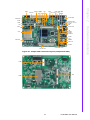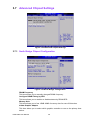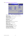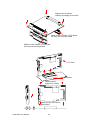
1
User Manual
PCM-9562
Copyright
The documentation and the software included with this product are copyrighted 2010
by Advantech Co., Ltd. All rights are reserved. Advantech Co., Ltd. reserves the right
to make improvements in the products described in this manual at any time without
notice. No part of this manual may be reproduced, copied, translated or transmitted
in any form or by any means without the prior written permission of Advantech Co.,
Ltd. Information provided in this manual is intended to be accurate and reliable. However, Advantech Co., Ltd. assumes no responsibility for its use, nor for any infringements of the rights of third parties, which may result from its use.
Acknowledgements
Award is a trademark of Award Software International, Inc.
VIA is a trademark of VIA Technologies, Inc.
IBM, PC/AT, PS/2 and VGA are trademarks of International Business Machines Corporation.
Intel and Pentium are trademarks of Intel Corporation.
Microsoft Windows is a registered trademark of Microsoft Corp.
RTL is a trademark of Realtek Semi-Conductor Co., Ltd.
ESS is a trademark of ESS Technology, Inc.
UMC is a trademark of United Microelectronics Corporation.
SMI is a trademark of Silicon Motion, Inc.
Creative is a trademark of Creative Technology LTD.
CHRONTEL is a trademark of Chrontel Inc.
All other product names or trademarks are properties of their respective owners.
PCM-9562 User Manual
Part No. 2006956212
Edition 3
Printed in China
March 2011
ii
Product Warranty (2 years)
Advantech warrants to you, the original purchaser, that each of its products will be
free from defects in materials and workmanship for two years from the date of purchase.
This warranty does not apply to any products which have been repaired or altered by
persons other than repair personnel authorized by Advantech, or which have been
subject to misuse, abuse, accident or improper installation. Advantech assumes no
liability under the terms of this warranty as a consequence of such events.
Because of Advantech’s high quality-control standards and rigorous testing, most of
our customers never need to use our repair service. If an Advantech product is defective, it will be repaired or replaced at no charge during the warranty period. For outof-warranty repairs, you will be billed according to the cost of replacement materials,
service time and freight. Please consult your dealer for more details.
If you think you have a defective product, follow these steps:
1. Collect all the information about the problem encountered. (For example, CPU
speed, Advantech products used, other hardware and software used, etc.) Note
anything abnormal and list any onscreen messages you get when the problem
occurs.
2. Call your dealer and describe the problem. Please have your manual, product,
and any helpful information readily available.
3. If your product is diagnosed as defective, obtain an RMA (return merchandise
authorization) number from your dealer. This allows us to process your return
more quickly.
4. Carefully pack the defective product, a fully-completed Repair and Replacement
Order Card and a photocopy proof of purchase date (such as your sales receipt)
in a shippable container. A product returned without proof of the purchase date
is not eligible for warranty service.
5. Write the RMA number visibly on the outside of the package and ship it prepaid
to your dealer.
Declaration of Conformity
FCC Class B
This equipment has been tested and found to comply with the limits for a Class B digital device, pursuant to part 15 of the FCC Rules. These limits are designed to provide reasonable protection against harmful interference in a residential installation.
This equipment generates, uses and can radiate radio frequency energy and, if not
installed and used in accordance with the instructions, may cause harmful interference to radio communications. However, there is no guarantee that interference will
not occur in a particular installation. If this equipment does cause harmful interference to radio or television reception, which can be determined by turning the equipment off and on, the user is encouraged to try to correct the interference by one or
more of the following measures:
Reorient or relocate the receiving antenna.
Increase the separation between the equipment and receiver.
Connect the equipment into an outlet on a circuit different from that to which the
receiver is connected.
Consult the dealer or an experienced radio/TV technician for help.
iii
PCM-9562 User Manual
Technical Support and Assistance
1.
2.
Visit the Advantech web site at www.advantech.com/support where you can find
the latest information about the product.
Contact your distributor, sales representative, or Advantech's customer service
center for technical support if you need additional assistance. Please have the
following information ready before you call:
– Product name and serial number
– Description of your peripheral attachments
– Description of your software (operating system, version, application software,
etc.)
– A complete description of the problem
– The exact wording of any error messages
Warnings, Cautions and Notes
Warning! Warnings indicate conditions, which if not observed, can cause personal
injury!
Caution! Cautions are included to help you avoid damaging hardware or losing
data. e.g.
There is a danger of a new battery exploding if it is incorrectly installed.
Do not attempt to recharge, force open, or heat the battery. Replace the
battery only with the same or equivalent type recommended by the manufacturer. Discard used batteries according to the manufacturer's
instructions.
Note!
Notes provide optional additional information.
Document Feedback
To assist us in making improvements to this manual, we would welcome comments
and constructive criticism. Please send all such - in writing to: [email protected]
Packing List
Before setting up the system, check that the items listed below are included and in
good condition. If any item does not accord with the table, please contact your dealer
immediately.
1 x PCM-9562 SBC
1 x Startup manual
1 x Utility CD
1 x ATX 5VSB CABLE
1700015741
1 x mini jumper pack
9689000002
PCM-9562 User Manual
iv
Ordering Information
Model Number Description
PCM-9562D-S6A1E
D510+ICH8M 2GbE/5COM/3SATAII/CFII/M-PCIe
PCM-9562N-S6A1E
N450+ICH8M 2GbE/5COM/3SATAII/CFII/M-PCIe
PCM-9562DF-S6A1E
D510+ICH8M 3GbE/6COM/3SATAII/CFII/M-PCIe
PCM-9562NF-S6A1E
N450+ICH8M 3GbE/6COM/3SATAII/CFII/M-PCIe
Model
CPU
Memory LVDS GbE
GbE3
Operating
WDT HD Audio USB2.0 RS-232 RS-422/485 PC-104+ Mini-PCIe Thermal
UL60601
Temperature
PCM-9562N-S6A1E
N450 SO_DIMM 18-bit
2
-
1
HD
8
3
2
Yes
1
Passive
PCM-9562D-S6A1E
D510 SO_DIMM 18-bit
2
-
1
HD
8
3
2
Yes
1
Active
0-60°C
0-60°C
PCM-9562NF-S6A1E
N450 SO_DIMM 18-bit
2
1
2
HD
8
3+1
2
Yes
1
Passive
0-60°C
PCM-9562DF-S6A1E
D510 SO_DIMM 18-bit
2
1
2
HD
8
3+1
2
Yes
1
Active
0-60°C
PCM-9562NZ-1GS6A1E N450 Bundle 1GB 18-bit
2
Optional
1
HD
8
3
2
Yes
1
Passive
-20-80°C
PCM-9562Z2-1GS6A1E N450 Bundle 1GB 18-bit
2
Optional
1
HD
8
3
2
Yes
1
Passive
-40-85°C
Optional Accessories
Part Number
Description
PCM-10586-9562E
Wiring kit for PCM-9562 Series
PCM-110-00A3E
1-slot PCI riser card for 5.25" biscuits
PCM-120-00A3E
2-slot PCI riser card for 5.25" biscuits
PCM-200-00A2E
PC/104-Plus to PCI bus module
CF-HDD-ADP
CompactFlash 50-pin to IDE 44-pin adapter
1960049954N001
Hearspreader 157.4 x 100 x 24 mm
v
PCM-9562 User Manual
Safety Instructions
1.
2.
3.
Read these safety instructions carefully.
Keep this User Manual for later reference.
Disconnect this equipment from any AC outlet before cleaning. Use a damp
cloth. Do not use liquid or spray detergents for cleaning.
4. For plug-in equipment, the power outlet socket must be located near the equipment and must be easily accessible.
5. Keep this equipment away from humidity.
6. Put this equipment on a reliable surface during installation. Dropping it or letting
it fall may cause damage.
7. The openings on the enclosure are for air convection. Protect the equipment
from overheating. DO NOT COVER THE OPENINGS.
8. Make sure the voltage of the power source is correct before connecting the
equipment to the power outlet.
9. Position the power cord so that people cannot step on it. Do not place anything
over the power cord.
10. All cautions and warnings on the equipment should be noted.
11. If the equipment is not used for a long time, disconnect it from the power source
to avoid damage by transient overvoltage.
12. Never pour any liquid into an opening. This may cause fire or electrical shock.
13. Never open the equipment. For safety reasons, the equipment should be
opened only by qualified service personnel.
14. If one of the following situations arises, get the equipment checked by service
personnel:
The power cord or plug is damaged.
Liquid has penetrated into the equipment.
The equipment has been exposed to moisture.
The equipment does not work well, or you cannot get it to work according to
the user's manual.
The equipment has been dropped and damaged.
The equipment has obvious signs of breakage.
15. DO NOT LEAVE THIS EQUIPMENT IN AN ENVIRONMENT WHERE THE
STORAGE TEMPERATURE MAY GO BELOW -20° C (-4° F) OR ABOVE 60° C
(140° F). THIS COULD DAMAGE THE EQUIPMENT. THE EQUIPMENT
SHOULD BE IN A CONTROLLED ENVIRONMENT.
16. CAUTION: DANGER OF EXPLOSION IF BATTERY IS INCORRECTLY
REPLACED. REPLACE ONLY WITH THE SAME OR EQUIVALENT TYPE
RECOMMENDED BY THE MANUFACTURER, DISCARD USED BATTERIES
ACCORDING TO THE MANUFACTURER'S INSTRUCTIONS.
The sound pressure level at the operator's position according to IEC 704-1:1982 is
no more than 70 dB (A).
DISCLAIMER: This set of instructions is given according to IEC 704-1. Advantech
disclaims all responsibility for the accuracy of any statements contained herein.
PCM-9562 User Manual
vi
Wichtige Sicherheishinweise
1.
2.
3.
Bitte lesen sie Sich diese Hinweise sorgfältig durch.
Heben Sie diese Anleitung für den späteren Gebrauch auf.
Vor jedem Reinigen ist das Gerät vom Stromnetz zu trennen. Verwenden Sie
Keine Flüssig-oder Aerosolreiniger. Am besten dient ein angefeuchtetes Tuch
zur Reinigung.
4. Die NetzanschluBsteckdose soll nahe dem Gerät angebracht und leicht
zugänglich sein.
5. Das Gerät ist vor Feuchtigkeit zu schützen.
6. Bei der Aufstellung des Gerätes ist auf sicheren Stand zu achten. Ein Kippen
oder Fallen könnte Verletzungen hervorrufen.
7. Die Belüftungsöffnungen dienen zur Luftzirkulation die das Gerät vor überhitzung schützt. Sorgen Sie dafür, daB diese Öffnungen nicht abgedeckt werden.
8. Beachten Sie beim. AnschluB an das Stromnetz die AnschluBwerte.
9. Verlegen Sie die NetzanschluBleitung so, daB niemand darüber fallen kann. Es
sollte auch nichts auf der Leitung abgestellt werden.
10. Alle Hinweise und Warnungen die sich am Geräten befinden sind zu beachten.
11. Wird das Gerät über einen längeren Zeitraum nicht benutzt, sollten Sie es vom
Stromnetz trennen. Somit wird im Falle einer Überspannung eine Beschädigung
vermieden.
12. Durch die Lüftungsöffnungen dürfen niemals Gegenstände oder Flüssigkeiten in
das Gerät gelangen. Dies könnte einen Brand bzw. elektrischen Schlag auslösen.
13. Öffnen Sie niemals das Gerät. Das Gerät darf aus Gründen der elektrischen
Sicherheit nur von authorisiertem Servicepersonal geöffnet werden.
14. Wenn folgende Situationen auftreten ist das Gerät vom Stromnetz zu trennen
und von einer qualifizierten Servicestelle zu überprüfen:
15. Netzkabel oder Netzstecker sind beschädigt.
16. Flüssigkeit ist in das Gerät eingedrungen.
17. Das Gerät war Feuchtigkeit ausgesetzt.
18. Wenn das Gerät nicht der Bedienungsanleitung entsprechend funktioniert oder
Sie mit Hilfe dieser Anleitung keine Verbesserung erzielen.
19. Das Gerät ist gefallen und/oder das Gehäuse ist beschädigt.
20. Wenn das Gerät deutliche Anzeichen eines Defektes aufweist.
21. VOSICHT: Explisionsgefahr bei unsachgemaben Austausch der Batterie.Ersatz
nur durch densellben order einem vom Hersteller empfohlene-mahnlichen Typ.
Entsorgung gebrauchter Batterien navh Angaben des Herstellers.
22. ACHTUNG: Es besteht die Explosionsgefahr, falls die Batterie auf nicht fachmännische Weise gewechselt wird. Verfangen Sie die Batterie nur gleicher oder
entsprechender Type, wie vom Hersteller empfohlen. Entsorgen Sie Batterien
nach Anweisung des Herstellers.
23. Der arbeitsplatzbezogene Schalldruckpegel nach DIN 45 635 Teil 1000 beträgt
70dB(A) oder weiger.
Haftungsausschluss: Die Bedienungsanleitungen wurden entsprechend der IEC704-1 erstellt. Advantech lehnt jegliche Verantwortung für die Richtigkeit der in
diesem Zusammenhang getätigten Aussagen ab.
vii
PCM-9562 User Manual
Safety Precaution - Static Electricity
Follow these simple precautions to protect yourself from harm and the products from
damage.
To avoid electrical shock, always disconnect the power from your PC chassis
before you work on it. Don't touch any components on the CPU card or other
cards while the PC is on.
Disconnect power before making any configuration changes. The sudden rush
of power as you connect a jumper or install a card may damage sensitive electronic components.
PCM-9562 User Manual
viii
Contents
Chapter
Chapter
1
General Information ............................1
1.1
1.2
1.3
Introduction ............................................................................................... 2
Product Specifications............................................................................... 2
Chipset ...................................................................................................... 3
1.3.1 Functional Specifications .............................................................. 3
1.3.2 Mechanical Specifications............................................................. 5
1.3.3 Electrical Specifications ................................................................ 5
1.3.4 Environmental Specifications........................................................ 6
2
Hardware Installation ..........................7
2.1
Jumpers .................................................................................................... 8
2.1.1 Jumper List ................................................................................... 8
2.1.2 Jumper Settings ............................................................................ 8
2.1.3 Jumper Description ....................................................................... 9
Connectors.............................................................................................. 10
2.2.1 Connector List............................................................................. 10
2.2.2 Connector Settings ..................................................................... 11
Mechanical .............................................................................................. 15
2.3.1 Jumper and Connector Location................................................. 15
Figure 2.1 Jumper and Connector Layout (Component Side) ... 15
Figure 2.2 Jumper and Connector Layout (Solder Side) ........... 16
2.3.2 Board Dimensions....................................................................... 17
Figure 2.3 Board Dimension Layout (Component Side) ............ 17
Figure 2.4 Board Dimension Layout (Solder Side) .................... 18
2.2
2.3
Chapter
3
3.1
3.2
3.3
BIOS Settings.....................................19
Figure 3.1 Setup program initial screen..................................... 20
Entering Setup ........................................................................................ 20
Main Setup .............................................................................................. 20
Figure 3.2 Main setup screen .................................................... 21
3.2.1 System time / System date ......................................................... 21
Advanced BIOS Features Setup ............................................................. 21
Figure 3.3 Advanced BIOS features setup screen .................... 22
3.3.1 CPU Configuration ...................................................................... 22
Figure 3.4 CPU Configuration Setting ....................................... 22
3.3.2 IDE Configuration........................................................................ 23
Figure 3.5 IDE Configuration ..................................................... 23
3.3.3 Floppy Configuration................................................................... 24
Figure 3.6 Floppy Configuration ................................................ 24
3.3.4 Super I/O Configuration .............................................................. 24
Figure 3.7 Super I/O Configuration............................................ 24
3.3.5 Hardware Health Configuration................................................... 25
Figure 3.8 Hardware health configuration.................................. 25
3.3.6 ACPI Settings.............................................................................. 26
Figure 3.9 ACPI Settings ........................................................... 26
Figure 3.10General ACPI Configuration ..................................... 26
Figure 3.11Advanced ACPI Configuration.................................. 27
Figure 3.12Chipset ACPI Configuration...................................... 27
3.3.7 AHCI Configuration ..................................................................... 28
Figure 3.13Advanced ACPI Configuration.................................. 28
3.3.8 APM Configuration...................................................................... 29
ix
PCM-9562 User Manual
Figure 3.14APM Configuration ................................................... 29
Event Log Configuration ............................................................. 30
Figure 3.15South Bridge ACPI Configuration............................. 30
3.3.10 MPS Configuration...................................................................... 30
Figure 3.16South Bridge ACPI Configuration............................. 30
3.3.11 SMBIOS Configuration ............................................................... 31
Figure 3.17South Bridge ACPI Configuration............................. 31
3.3.12 USB Configuration ...................................................................... 31
Figure 3.18South Bridge ACPI Configuration............................. 31
Figure 3.19USB Mass storage Device Configuration ................. 32
Advanced PCI/PnP Settings ................................................................... 32
Figure 3.20PCI/PNP Setup (top) ................................................ 33
Boot Settings........................................................................................... 34
Figure 3.21Boot Setup Utility...................................................... 34
3.5.1 Boot settings Configuration......................................................... 34
Figure 3.22Boot Setting Configuration ....................................... 34
Security Setup......................................................................................... 35
Figure 3.23Password Configuration ........................................... 35
Advanced Chipset Settings..................................................................... 36
Figure 3.24Advanced Chipset Settings ...................................... 36
3.7.1 North Bridge Chipset Configuration ............................................ 36
Figure 3.25North Bridge Configuration....................................... 36
Figure 3.26Video function configuration ..................................... 37
3.7.2 South Bridge Chipset Configuration ........................................... 38
Figure 3.27South Bridge Configuration ...................................... 38
Exit Option .............................................................................................. 39
Figure 3.28Exit Option................................................................ 39
3.8.1 Save Changes and Exit .............................................................. 39
3.8.2 Discard Changes and Exit .......................................................... 39
3.8.3 Load Optimal Defaults ................................................................ 39
3.8.4 Load Fail-Safe Defaults .............................................................. 39
3.3.9
3.4
3.5
3.6
3.7
3.8
Chapter
4
Software Introduction & Installation 41
4.1
4.2
S/W Introduction ..................................................................................... 42
Driver Installation .................................................................................... 42
4.2.1 Windows XP Professional........................................................... 42
4.2.2 Other OS..................................................................................... 42
Value-Added Software Services ............................................................. 42
4.3.1 SUSI Introduction........................................................................ 42
4.3.2 Software APIs ............................................................................. 43
4.3.3 SUSI Utilities............................................................................... 44
4.3.4 SUSI Installation ......................................................................... 44
4.3.5 SUSI Sample Programs.............................................................. 46
4.3
Chapter
5
Extension I/O Installation ................. 53
Appendix A
Pin Assignments............................... 55
Appendix B
Optional Extras for PCM-9562 A1.... 77
B.1
PCM-10586-9562E Cable kit for PCM-9562 A1 ..................................... 78
Table B.1: PCM-10586-9562E Cable kit for PCM-9562 A1....... 78
Appendix C
Prog. GPIO & Watchdog Timer ........ 79
PCM-9562 User Manual
x
C.1
C.2
Watchdog Timer...................................................................................... 80
C.1.1 First Watchdog (SCH3106)......................................................... 80
C.1.2 Second Watchdog (MAX6369) ................................................... 81
GPIO Sample Code ................................................................................ 81
Appendix D
System Assignments ........................93
D.1
1st MB memory map ............................................................................... 94
Table D.1: 1st MB memory map ................................................ 94
DMA channel assignments ..................................................................... 94
Table D.2: DMA channel assignments....................................... 94
Interrupt assignments.............................................................................. 94
Table D.3: Interrupt assignments ............................................... 94
Table D.4: System I/O Ports ...................................................... 95
D.2
D.3
xi
PCM-9562 User Manual
PCM-9562 User Manual
xii
Chapter
1
1
General Information
1.1 Introduction
Intel® N450/D510 processor
EBX form factor standard, supports PC/104 plus
One SODIMM up to 2G DDR2 667/800MHz
Dual Display: VGA + LVDS
Supports 8 x USB 2.0 ports
Supports 3 x SATAII
Supports up to 6 x COM (Support Auto flow control)
Supports up to 2 x Watchdog Timer
Supports up to 3 x Intel Giga Ethernet support
UL60601 design in GbE3 and COM6 (Full version only, UL60601 cert is for
Medical )
Supports Wake-on-LAN, Wake-on-Modem
Power off protection and Software I2C API support
1.2 Product Specifications
General
CPU
N450/D510 1.6GHz
L2 Cache
512KB/1MB
System Chipset
N450/D510 + ICH8M
BIOS
AMI 16Mb SPI BIOS
System Memory
One SODIMM up to 2GB DDR2 667/800MHz
Power Management
APM1.2, ACPI support
SSD
CF card type I/II
Watchdog Timer
WD1: Can be IWD and PWD
10ms, disable, 1sec and 60sec interval timer
WD2: PWD (Full version only)
255-level interval timer, setup by software, Super I/O integrated, SMSC Controller
Expansion Interface
Supports PC-104 plus, PCI slot x1, Mini PCIe
Battery
Lithium 3 V / 196 mAH
I/O
I/O Interface
1 x CF, 3 x SATAII, 1 x K/B, 1 x Mouse, 4 x RS232 (COM6 ,UL60601
design, is full version only), 2 x RS232/422/485 (Default RS-422/485,
RS-232 with TX/RX only is optional by request), 1 x LPT
USB
8 x USB 2.0 compliant Ports
Audio
AC97, Line-in, Line-out, Mic-in, speaker out (R/L)
IrDA -
115kbps (optional by request) shared from COM2
GPIO
16-bit general purpose
Ethernet
Chipset
GbE1 : Intel 82567, GbE2 : Intel 82583V, Optional GbE3: Intel
82583V (UL60601 Compliant)
Speed
10/100/1000Mbps
Interface
3 (RJ-45 connector through the cable and GbE3 is full version only)
PCM-9562 User Manual
2
Display
Controller
Embedded Gen3.5+ GFX Core
Shared Memory Architecture up to 224 MB system memory
LVDS LCD
Single channel 18-bit LVDS up to WXGA 1366 x 768
VGA
Supports up to SXGA 1400 x 1050 @ 60 Hz for Atom N450, up
to 2048 x 1536 for Atom D510
Dual Independent Display
VGA+ LVDS
General Information
VRAM
1.3 Chipset
1.3.1 Functional Specifications
1.3.1.1 Processor
Intel N450/D510 processor 1.6GHz (512KB/ 1MB)
CPU Process: 45nm.
667/800 MHz FSB Support
1.3.1.2 Chipset
North Bridge
Controller Hub
Intel® N450/D510
FSB
667/800 MHz
Memory
DDRII 667/800 SDRAM
Display
Chipset
Intel® N450/D510 +ICH8M
Dual independent display
VGA+LVDS(18-bit) (Supports Clone and Twin mode)
VGA Memory
Up to 224 MB of dynamic video memory allocation
VGA:
Supports QXGA Up to 2048 x 1536
Display
LVDS:
Resolution up to 18 bpp, XGA (1024 x 768) and WXGA
(1280 x 800)
Internal Graphics Features
* Intel 3.5 Gen Integrated Graphic Engine + GFX core
* DVMT 3.0 (Dynamic Video Memory Technology)
* Directx* 9 compliant Pixel Shader 2.0
* 2 display ports: LVDS and VGA
* Intel® Clear Video Technology
1.3.1.3 Chipset (ICH8-M)
I/O Interface
LPT
1 (FDD is optional)
RS-232
4 (COM6 ,UL60601 design, is full version only)
RS-232/422/485
2 (RS-232 with TX/RX only is optional by request)
K/B
1
Mouse
1
USB
8 x USB 2.0
3
Chapter 1
IEEE 802.3u 100Base-T & IEEE 802.3ab 1000Base-T for 10/100/
1000Mbps optional
Standard
PCM-9562 User Manual
Audio
HD Audio, ALC888 Codec, Line-in, Line-out, Mic-in, speaker out (R/L)
(Supports 8Ω 1W or 4Ω 2 W Speaker for Speaker-out)
GPIO
16-bit GPIO
IrDA
115 kbps (optional by request) shared from COM2
South Bridge
Controller Hub
ICH8M
PCI Compliant
PCI 2.3
PCI Bus
* PCI masters
PC/104-Plus (ISA doesn't support DMA)
Other Features
* 8 x USB 2.0 ports, 480MB/s (all internal connectors)
Default: 500mA @ one port (Up to 1A @ 2 ports)
* 3 x SATAII (Max. Data transfer Rate 300MB/s)
* HD Audio CODEC (ALC888)
* Power Management (S0, S1, S3,S4, S5)
BIOS
16 Mb Flash BIOS via SPI
1.3.1.4 Others
Ethernet
Chipset
GbE 1 : Intel 82567V
GbE 2: Intel 82583V
GbE 3: Intel 82583V (UL60601 design, optional)
IEEE Compliant
Compliant with IEEE 802.3, IEEE 802.3u, IEEE 802.3x, IEEE
8023y, IEEE 802.ab
Disable LAN through BIOS
Yes
Driver Support
WES7/Windows XP/XP Embed/CE, Linux, QNX
Audio
Codec
HD Audio, ALC888 Codec
Connector
Line in, Line out, Mic in, Speak out (R/L, 8 Ohm 1W/4Ohm
2W)
Hardware Monitor
Super I/O
Fan
LPC I/O for onboard alarm
SCH3106
1. Smart FAN Support.
2. Programmable automatic fan monitor based on temperature.
3. 2 pin connector for LED indication when fan fail or system
abnormal.
4. System FAN Power Connector x 1
5. Reserve CPU FAN Power Connector x 1
Pin2: +12 V
Pin3: Fan speed signal input
Temperature
CPU Temperature
Voltage
3.3 V,+5 V, +12 V, Vcore
PCI to ISA
Chipset
ITE8888G (ISA DMA not supported)
Second watchdog timer
Pin -Selectable Watchdog
Timer
PCM-9562 User Manual
MAX6369KA-T Watchdog Timers
4
Chapter 1
1.3.2 Mechanical Specifications
1.3.2.1 Dimensions (mm)
203mm(L)*146mm(W) (8" x 5.75")
1.3.2.2 Height on Top (mm)
PCM-9562N-S6A1E: 15.4mm (PCI slot)
PCM-9562D-S6A1E: 25mm (CPU Cooler)
1.3.2.4 Heatsink/Cooler Dimensions (mm)
50*50*10 mm (Heatsink for PCM-9562N-S6A1E)
50*50*25 mm (Cooler for PCM-9562D-S6A1E)
50*50*30 mm (Heatsink for Extended temp product)
1.3.2.5 Weight (g) with Heatsink
850 g
1.3.3 Electrical Specifications
1.3.3.1 Power Supply Voltage
Power Type
AT/ATX
Power Supply Voltage
ATX: 12V/ 5V stand-by ± 10% (5V stand-by power is only for auto power off
function)
AT: 12 V ±10% only
1.3.3.2 Power Supply Current
Test Condition:
Add-in Card - None
MiniPCIe Card - None
HDD - 3.5" WD 80GB SATA2 *1
KeyBoard/Mouse - USB or PS/2 Interface
Display - VGA
Power Consumption (A or mA)
Condition
Voltage/
Condition
Power on - Boot DOS Idle
procedure
Mode
Win. Idle
Mode
BurnIn
(10minutes)
+12 V
926 mA
1037 mA
893 mA
1187 mA
5 VSB
9 mA
8 mA
8 mA
10 mA
5
Testing
Software
BurnIn
PCM-9562 User Manual
General Information
1.3.2.3 Height on Button (mm)
8.5mm (CF socket)
Condition
Power Consumption (A or mA)
Voltage/Condition
Boot to DOS prompt mode
CPU type:
Max. memory slot Qty: #
size/pcs: 256MB
+12 V
998 mA
5 VSB
8 mA
CPU type:
Max. memory slot Qty: #
size/pcs: 512 MB
+12 V
989 mA
5 VSB
8 mA
CPU type:
Max. memory slot Qty: #
size/pcs: 1GB
+12 V
1096 mA
5 VSB
8 mA
CPU type:
Max. memory slot Qty: #
size/pcs: 2 GB
+12 V
1058 mA
5 VSB
8 mA
1.3.3.3 RTC Battery
Typical Voltage: 3.0 V
Normal discharge capacity: 196 mAh
1.3.4 Environmental Specifications
1.3.4.1 Operating Temperature
Operating temperature: 0 ~ 60°C (32~140°F)
1.3.4.2 Operating Humidity
Operating Humidity: 0% ~ 90% Relative Humidity, non-condensing
1.3.4.3 Storage Temperature
Standard products (0~60°C)
Storage temperature: -20~70°C
1.3.4.4 Storage Relative Temperature
Standard products (0~60°C)
Relative humidity: 95% @ 60°C
Phoenix products (-20~80°C)
Relative humidity: 95% @ 60°C
Platinum Phoenix products (-40~85°C)
Relative humidity: 95% @ 60°C
PCM-9562 User Manual
6
Chapter
2
2
Hardware Installation
This chapter explains the setup procedures of the PCM-9562 A1 hardware, including
instructions on setting jumpers and connecting peripherals, switches, indicators and
mechanical drawings. Be sure to read all safety precautions before you begin the
installation procedure.
2.1 Jumpers
2.1.1 Jumper List
JP1
LCD Panel Power Select
JP2
VIO Select for PCI and PC104+ Slot
JP3
CMOS Clear
JP4
UART2 Mode Select
JP7
Mini PCIE Voltage Select
2.1.2 Jumper Settings
JP1
LCD Panel Power Select
Part Number
1653003101
Footprint
PH_3x1V_2.54mm
Description
PIN HEADER 3*1P 180D(M) 2.0mm DIP SQUARE W/O Pb
Setting
Function
(1-2)
+5 V
(2-3)*
+3.3 V
JP2
VIO Select for PCI and PC104+ Slot
Part Number
1653003100
Footprint
PH3x1P-2.54
Description
PIN HEADER 3*1P 180D(M) 2.54mm DIP WO/Pb
Setting
Function
(1-2)*
+5 V
(2-3)
+3.3 V
JP3
CMOS Clear
Part Number
1653003101
Footprint
HD_3x1P_79_D
Description
PIN HEADER 3*1P 180D(M) 2.0mm DIP SQUARE W/O Pb
Setting
Function
(1-2)*
Normal
(2-3)
Clear
JP4
UART2 Mode Select
Part Number
1653002101
Footprint
HD_2x1P_79_D
Description
PIN HEADER 2*1P 180D(M)SQUARE 2.0mm DIP W/O Pb
Setting
Function
(1-2)*
COM2
NL
IrDA
PCM-9562 User Manual
8
Mini PCIE Voltage Select
Part Number
1653003100
Footprint
HD_3x1P_100_D
Description
PIN HEADER 3*1P 180D(M) 2.54mm DIP WO/Pb
Setting
Function
(1-2)*
+3.3 V
(2-3)
+3.3 V Dual
Cards can be configured by setting jumpers. A jumper is a metal bridge used to close
an electric circuit. It consists of two metal pins and a small metal clip (often protected
by a plastic cover) that slides over the pins to connect them. To close a jumper, you
connect the pins with the clip. To open a jumper, you remove the clip. Sometimes a
jumper will have three pins, labeled 1, 2 and 3. In this case you would connect either
pins 1 and 2, or 2 and 3.
The jumper settings are schematically depicted in this manual as follows.
A pair of needle-nose pliers may be helpful when working with jumpers. If you have
any doubts about the best hardware configuration for your application, contact your
local distributor or sales representative before you make any changes.
Warning! To avoid damaging the computer, always turn off the power supply
before setting jumpers to clear CMOS. Before turning on the power supply, set the jumper back to 3.0 V Battery On.
9
PCM-9562 User Manual
Hardware Installation
2.1.3 Jumper Description
Chapter 2
JP7
2.2 Connectors
2.2.1 Connector List
CN1
CN2
CN4
CN5
CN6
CN8
CN9
CN10
CN11
CN12
CN13
CN14
CN15
CN16
CN17
CN18
CN20
CN21
CN22
CN23
CN24
CN25
CN26
CN28
CN29
CN30
CN31
CN32
CN33
CN34
CN35
CN36
CN37
CN38
CN39
CN40
CN41
CN42
CN43
CN44
CN45
CN46
FAN1
FAN2
PCI1
PCM-9562 User Manual
DDR2 SODIMM Socket
Audio CD-In Connector
Audio Connector
Power Connector
Inverter Connector
VGA Connector
LVDS Connector
GbE1 Connector
GbE1,2 LED Connector
GbE2 Connector
HDD LED and POWER LED Connector
GbE3 Connector
LPT / FDD Connector
Standby Power Connector
PC-104/+ Connector
GbE3 LED Connector
USB1/2 Connector
USB3/4 Connector
Reset Button Connector
Power Button Connector
SIR Connector
PS2 Keyboard/Mouse Connector
CF TYPEII Connector
USB5/6 Connector
USB7/8 Connector
Mini PCIE Slot
Mini PCIE Lock
SATA 1 Connector
SATA 2 Connector
SATA 3 Connector
GPIO1 Connector
GPIO2 Connector
SMBUS Connector
I2C Connector
COM1 Connector
COM2 Connector
COM3 Connector
COM4/5 (422/485) Connector
COM6 Connector
-5 V and -12 V Connector
SPI Flash Socket
SATA Power Connector
System Fan Connector
CPU Fan Connector
PCI SLOT
10
Audio CD-In Connector (CN16)
CD In cable used to send audio CD sound to the computer's audio chipset via CN16.
Audio Connector (CN4)
The Audio link is a 2x8 pin connector, the PCM-9562 can support speaker-out, LineIN, Line-out with Realtek ALC888, HD audio. Detailed pin assignments refer to
Appendix A.
1. ATX power supply:
You can use standard 4 pins 12V power output from power supply directly to connect
to CN5. For auto power off feature, you should use cable 1700015741 connecting to
CN16 (Standby Power Connector) to provide 5VSB power input.
2. AT power supply:
You can use standard 4 pins 12V power output from power supply directly to connect
to CN5.
Inverter Connector (CN6)
PCM-9562 can provide +5 V and +12 V and signal to LCD inverter board via CN6.
VGA Connector (CN8)
The DB15-pin female connector is provided for video monitors.
LVDS Connector (CN9)
Low-voltage differential signaling, or LVDS, is an electrical signaling system that
can run at very high speeds over inexpensive twisted-pair copper cables. LVDS is a
differential signaling system, which means that it transmits two different voltages
which are compared at the receiver. LVDS uses this difference in voltage between
the two wires to encode the information.
PCM-9562 supports 18bit LVDS panel via CN9.
Ethernet Connector (CN10, CN12, CN14)
For the Ethernet port, PCM-9562 equipped with 3 high performance giga ethernet
ports which are fully compliant with IEEE 802.3ab 1000Base-T. It is supported by all
major network operating systems.
GbE1/2 LED connector (CN11)
CN11 is a connector for GbE1 and GbE2 indication LED.
HDD LED and POWER LED Connector (CN13)
CN13 is a front panel connector to indicate power and HDD status.
11
PCM-9562 User Manual
Hardware Installation
Power Connector (CN5)
PCM-9562 can support both ATX and AT power supply.
Chapter 2
2.2.2 Connector Settings
LPT Connector (CN14)
PCM-9562 can support LPT or Floppy via CN15. LPT (Line Print Terminal) is the
original, yet still common, name of the parallel port interface on IBM PC-compatible
computers. It was designed to operate a text printer that used IBM's 8-bit extended
ASCII character set.
Standby Power Connector (CN16)
PCM-9562 can support both ATX and AT power supply.
1. ATX power supply:
You can use standard 4 pins 12 V power output from power supply directly to connect
to CN5. For auto power off feature, you should use cable 1700015741 connect to
CN16 (Standby Power Connector) to provide 5VSB power input.
2. AT power supply:
You can use standard 4 pins 12 V power output from power supply directly to connect
to CN5.
PC104 plus Connector (CN17)
PCM-9562 supports PC-104 plus and it includes PCI and ISA interface which are follow PC-104 standard. It is intended for industrial embedded computing environments
where applications depend on reliable data acquisition.
GbE3 LED Connector (CN18)
CN18 is a connector for GbE3 indication LED.
USB Connectors (CN20, CN21, CN28, CN29)
The board provides up to 8* USB (Universal Serial Bus) ports. This gives complete
Plug and Play, and hot attach/detach for up to 127 external devices. The USB interfaces comply with USB specification Rev. 2.0 which supports 480Mbps transfer rate,
and are fuse protected.
Reset Button Connector (CN22)
CN22 is for system reset button. System reset clears any pending errors or events
and bring a system to normal condition or initial state.
Power Button Connector (CN23)
CN23 is 2 pin wafer type connector and support to turn on/off system.
SIR Connector (CN24)
The boards can support IrDA function (optional by request). The function is shared
from COM2 and data transfer rate is up to 115kbps.
PCM-9562 User Manual
12
Mini PCIe Connector (CN30)
PCI Express Mini Card (also known as Mini PCI Express, Mini PCIe, and Mini PCI-E)
is a replacement for the Mini PCI form factor based on PCI Express. It is developed
by the PCI-SIG. The host device supports both PCI Express and USB 2.0 connectivity, and each card uses whichever the designer feels most appropriate to the task.
PCM-9562 support a Mini PCIe slot.
SATA Connector (CN32, CN33 and CN34)
PCM-9562 comply Serial ATA 2.5 spec and data transfer rates up to 300 MB/s,
enabling very fast data and file transfer, and independent DMA operation on two
ports.
The Serial Advanced Technology Attachment computer bus has the primary function
of transferring data between the motherboard and mass storage devices (such as
hard disk drives and optical drives) inside a computer.
GPIO Connector (CN35 and CN36)
GPIO is General Purpose Input Output. PCM-9562 supports 16-bit programmable I/O
via CN35 and CN36. These GPIO pin can be programmed as data input pin or output
control signal pin to control device.
SMBus Connector (CN37)
The System Management Bus (abbreviated to SMBus or SMB) is a simple two-wire
bus, derived from I2C and used for communication with low-bandwidth devices on a
motherboard, especially power related chips such as a laptop's rechargeable battery
subsystem (see Smart Battery Data). Other devices might include temperature, fan
or voltage sensors, lid switches and clock chips. PCI add-in cards may connect to a
SMBus segment.
The SMBus was defined by Intel in 1995. It carries clock, data, and instructions and
is based on Philips' I2C serial bus protocol. Its clock frequency range is 10 kHz to 100
kHz. Its voltage levels and timings are more strictly defined than those of I2C, but
devices belonging to the two systems are often successfully mixed on the same bus.
I2C connector (CN38)
13
PCM-9562 User Manual
Hardware Installation
CF TYPE I/II Connector (CN26)
CompactFlash (CF) is a mass storage device format used in portable electronic
devices. For storage, CompactFlash typically uses flash memory in a standardized
enclosure. PCM-9562 has CF slot and it can support CompactFlash card type I/II.
Chapter 2
PS/2 keyboard and mouse Connector (CN25)
PCM-9562 can support PS/2 keyboard and mouse via CN25. The PS/2 connector is
used for connecting some keyboards and mouse to a PC compatible computer system. Its name comes from the IBM Personal System/2 series of personal computers,
with which it was introduced in 1987. The PS/2 mouse connector generally replaced
the older DE-9 RS-232 "serial mouse" connector, while the keyboard connector
replaced the larger 5-pin DIN used in the IBM PC/AT design.
I2C (Inter-Integrated Circuit) is a multi-master serial computer bus invented by Philips
that is used to attach low-speed peripherals to a motherboard, embedded system, or
cellphone. The name is pronounced eye-squared-see or eye-two-see.
I2C uses only two bidirectional open-drain lines, Serial Data (SDA) and Serial Clock
(SCL), pulled up with resistors. Typical voltages used are +5 V or +3.3 V although
systems with other, higher or lower, voltages are permitted.
The I2C reference design has a 7-bit address space with 16 reserved addresses, so
a maximum of 112 nodes can communicate on the same bus.
COM port connector (CN39, CN40, CN41, CN42 and CN43)
COM is the original, yet still common, name of the serial port interface on IBM PCcompatible computers.PCM-9562 can support 4 RS-232 ports (CN39, CN40, CN41,
CN43) and 2 RS-422/485 (CN42). COM6 (CN43) is photo isolated and complies with
UL60601.
-5 V and -12 V Connector (CN44)
CN44 is a wafer type 3-pin connector for -5 V and -12 V.
SPI Flash socket (CN45)
CN45 is a socket for BIOS flash. PCM-9562 uses a 16Mbit capacity flash for BIOS.
SATA Power Connecter (CN46)
CN46 is SATA Power Connecter
2.3 Mechanical
2.3.1 Jumper and Connector Location
CN14
CN6
PCI1
CN36
JP2
JP1 GPIO1/2 JP7
CN10
CN11
CN11 CN23
CN44
CN22
CN5
CN18
CN4
FAN1
CN9
CN46
CN16
CN24
JP3
CN32/3/34
CN2
JP4
CN40
CN41
CN42
CN8
CN39
CN15
CN26
FAN2
CN20/21/28/29
CN43
CN13
CN17
PCM-9562 User Manual
14
Inverter SMBus
PCI Slot
JP1
JP2
GPIO JP7
LAN1
LAN2 PWR BTN
LAN1/2 LED
-5/-12V
Reset
Power input
LAN3 LED
Audio
System FAN
LVDS
Chapter 2
LAN3
SATA Power connector
5VSB
SIR
JP3
SATA 1/2/3
JP4
COM 2
COM 3
COM 4/5
VGA
COM 1
LPT
KB/MS
CPU FAN
USB 1~8
COM 6
Power/HDD LED
PC-104 Plus
Figure 2.1 Jumper and Connector Layout (Component Side)
CN30
CN1
CN26
15
PCM-9562 User Manual
Hardware Installation
CD-In
Figure 2.2 Jumper and Connector Layout (Solder Side)
193.04 [7.600]
144.78 [5.700]
78.74 [3.100]
71.12 [2.800]
5.08 [0.200]
0.00 [0.000]
36.20 [1.425]
2.3.2 Board Dimensions
140.97 [5.550]
138.44 [5.450]
135.89 [5.350]
135.89 [5.350]
88.26 [3.475]
82.25 [3.238]
72.48 [2.854]
31.48 [1.239]
2.54 [0.100]
0.00 [0.000]
5.08 [0.200]
193.04 [7.600]
147.32 [5.800]
152.40 [6.000]
62.23 [2.450]
67.31 [2.650]
68.58 [2.700]
41.25 [1.624]
5.08 [0.200]
0.00 [0.000]
0.25 [0.010]
2.54 [0.100]
0.00 [0.000]
2.54 [0.100]
Figure 2.3 Board Dimension Layout (Component Side)
PCM-9562 User Manual
16
0.00 [0.000]
113.66 [4.475]
193.04 [7.600]
Chapter 2
140.97 [5.550]
135.89 [5.350]
135.89 [5.350]
121.78 [4.794]
16.75 [0.659]
0.00 [0.000]
5.08 [0.200]
0.00 [0.000]
5.08 [0.200]
48.87 [1.924]
119.07 [4.688]
198.12 [7.800]
193.04 [7.600]
0.00 [0.000]
5.08 [0.200]
Figure 2.4 Board Dimension Layout (Solder Side)
17
PCM-9562 User Manual
Hardware Installation
39.05 [1.537]
PCM-9562 User Manual
18
Chapter
3
BIOS Settings
3
AMIBIOS has been integrated into many motherboards for over a decade. With the
AMIBIOS Setup program, you can modify BIOS settings and control the various system features. This chapter describes the basic navigation of the PCM-9562 BIOS
setup screens.
Figure 3.1 Setup program initial screen
AMI’s BIOS ROM has a built-in Setup program that allows users to modify the basic
system configuration. This information is stored in battery-backed CMOS so it retains
the Setup information when the power is turned off.
3.1 Entering Setup
Turn on the computer and check for the “patch” code. If there is a number assigned to
the patch code, it means that the BIOS supports your CPU. If there is no number
assigned to the patch code, please contact an Advantech application engineer to
obtain an up-to-date patch code file. This will ensure that your CPU’s system status is
valid. After ensuring that you have a number assigned to the patch code, press
<DEL> and you will immediately be allowed to enter Setup.
3.2 Main Setup
When you first enter the BIOS Setup Utility, you will enter the Main setup screen. You
can always return to the Main setup screen by selecting the Main tab. There are two
Main Setup options. They are described in this section. The Main BIOS Setup screen
is shown below.
PCM-9562 User Manual
20
Chapter 3
3.2.1 System time / System date
Use this option to change the system time and date. Highlight System Time or System Date using the <Arrow> keys. Enter new values through the keyboard. Press the
<Tab> key or the <Arrow> keys to move between fields. The date must be entered in
MM/DD/YY format. The time must be entered in HH:MM:SS format.
3.3 Advanced BIOS Features Setup
Select the Advanced tab from the PCM-9562 setup screen to enter the Advanced
BIOS Setup screen. You can select any of the items in the left frame of the screen,
such as CPU Configuration, to go to the sub menu for that item. You can display an
Advanced BIOS Setup option by highlighting it using the <Arrow> keys. All Advanced
BIOS Setup options are described in this section. The Advanced BIOS Setup
screens is shown below. The sub menus are described on the following pages.
21
PCM-9562 User Manual
BIOS Settings
Figure 3.2 Main setup screen
The Main BIOS setup screen has two main frames. The left frame displays all the
options that can be configured. Grayed-out options cannot be configured; options in
blue can. The right frame displays the key legend.
Above the key legend is an area reserved for a text message. When an option is
selected in the left frame, it is highlighted in white. Often a text message will accompany it.
Figure 3.3 Advanced BIOS features setup screen
3.3.1 CPU Configuration
Figure 3.4 CPU Configuration Setting
Max CPUID Value Limit
This item allows you to limit CPUID maximum value.
Execute-Disable Bit Capability
This item allows you to enable or disable the No-Execution page protection technology.
Hyper Threading Technology
This item allows you to enable or disable Intel Hyper Threading technology.
Intel® SpeedStepTM tech
When set to disabled, the CPU runs at its default speed, when set to enabled, the
CPU speed is controlled by the operating system.
PCM-9562 User Manual
22
3.3.2 IDE Configuration
Chapter 3
Intel® C-STATE tech
This item allows the CPU to save more power under idle mode.
Enhanced C-States
CPU idle set to enhanced C-States, disabled by Intel® C-STATE tech item.
BIOS Settings
Figure 3.5 IDE Configuration
ATA/IDE Configuration
This item allows you to select Disabled / Compatible / Enhanced.
Legacy IDE Channels
When set to Enhanced mode you can select IDE or AHCI mode. When select Compatible mode you can select SATA only / SATA pri, PATA sec or PATA only.
Primary/Secondary/Third IDE Master/Slave
BIOS auto detects the presence of IDE device, and displays the status of auto detection of IDE device.
Type: Select the type of SATA driver.[Not Installed][Auto][CD/DVD][ARMD]
LBA/Large Mode: Enables or Disables the LBA mode.
Block (Multi-Sector Transfer): Enables or disables data multi-sectors transfers.
PIO Mode: Select the PIO mode.
DMA Mode: Select the DMA mode.
S.M.A.R.T.: Select the smart monitoring, analysis, and reporting technology.
32Bit Data Transfer: Enables or disables 32-bit data transfer.
Hard Disk Write Protect
Disable/Enable device write protection. This will be effective only if device is
accessed through BIOS.
IDE Detect Time Out (Sec)
This item allows you to select the time out value for detecting ATA/ATAPI device(s).
23
PCM-9562 User Manual
3.3.3 Floppy Configuration
Figure 3.6 Floppy Configuration
Floppy B
Select the type of floppy drive, if any, connected to the system. We suggest you disable the floppy if installing Windows Vista without a floppy drive.
3.3.4 Super I/O Configuration
Figure 3.7 Super I/O Configuration
Serial Port1 / Port2 / Port3 / Port 4 / Port 5 / Port 6 address
This item allows you to select serial port1 ~ port6 of base addresses.
Serial Port1 / Port2 / Port3 / Port 4 / Port 5 / Port 6 IRQ
This item allows you to select serial port1 ~ port6 of IRQ.
Serial port2 Mode
This option configures serial port 2 mode.
PCM-9562 User Manual
24
Figure 3.8 Hardware health configuration
H/W Health Function
This item allows you to control H/W monitoring.
Temperature & Voltage show
CPU/System Temperature
Vcore / +3.3Vin / +5Vin / +12Vin / VBAT
25
PCM-9562 User Manual
BIOS Settings
3.3.5 Hardware Health Configuration
Chapter 3
Auto Flow Control Port4 / Port5
This item allows you to enable or disable auto flow control function.
COM4 / COM5 RS422/485 Control
This item allows you to select RS422 or RS485 control.
Parallel Port Address
This item allows you to select parallel port of base addresses.
Parallel Port Mode
This item allows you to select parallel port of mode.
Parallel Port IRQ
This item allows you to select parallel port of IRQ.
LPT/FDD Switch
This function will switch LPT port to FDD mode.
WatchDog Function
WatchDog function support (Seconds/Minutes).
3.3.6 ACPI Settings
Figure 3.9 ACPI Settings
3.3.6.1 General ACPI Configuration
Figure 3.10 General ACPI Configuration
Suspend mode
Select the ACPI state used for system suspend.
Report Video on S3 Resume
This item allows you to invoke VA BIOS POST on S3/STR resume.
PCM-9562 User Manual
26
Chapter 3
3.3.6.2 Advanced ACPI Configuration
3.3.6.3 Chipset ACPI Configuration
Figure 3.12 Chipset ACPI Configuration
27
PCM-9562 User Manual
BIOS Settings
Figure 3.11 Advanced ACPI Configuration
ACPI Version Features
This item allows you to enable RSDP pointers to 64-bit fixed system description
tables.
ACPI APIC support
Include APIC table pointer to RSDT pointer list.
AMI OEMB table
Include OEMB table pointer to R(x)SDT pointer lists.
Headless mode
Enable / Disable Headless operation mode through ACPI.
Energy Lake Feature
Allows you to configure Intel's Energy Lake power management technology.
APIC ACPI SCI IRQ
Enable/Disable APIC ACPI SCI IRQ.
USB Device Wakeup From S3/S4
Enable/Disable USB Device Wakeup from S3/S4.
High Performance Event Timer
Enable/Disable High performance Event timer.
3.3.7 AHCI Configuration
Figure 3.13 Advanced ACPI Configuration
AHCI Ports0 / Port1 / Port2
While entering setup, BIOS auto detects the presence of IDE devices. This displays
the status of auto detection of IDE device.
PCM-9562 User Manual
28
Chapter 3
3.3.8 APM Configuration
BIOS Settings
Figure 3.14 APM Configuration
Power Management/APM
Enable or disable APM.
Power Button Mode
Power on, off, or enter suspend mode when the power button is pressed. The following options are also available.
Restore on AC power Loss
Use this to set up the system response after a power failure. The "Off" setting keeps
the system powered off after power failure, the "On" setting boots up the system after
failure, and the "Last State" returns the system to the status just before power failure.
Video Power Down Mode
Power down video in suspend or standby mode.
Hard Disk Power Down Mode
Power down Hard Disk in suspend or standby mode.
Standby Time Out
Go into standby in the specified time.
Suspend Time Out
Go into Suspend in the specified time.
Resume On Ring
Enable / Disable RI to generate a wake event.
Resume On PME#
Enable / Disable PME to generate a wake event.
Resume On RTC Alarm
Enable / Disable RTC to generate a wake event.
29
PCM-9562 User Manual
3.3.9 Event Log Configuration
Figure 3.15 South Bridge ACPI Configuration
View Event Log
View all unread events on the event Log.
Mark all events as read
Mark all unread events as read.
Clear Event Log
Discard all events in the event Log.
3.3.10 MPS Configuration
Figure 3.16 South Bridge ACPI Configuration
MPS Revision
This item allows you to select MPS reversion.
PCM-9562 User Manual
30
Chapter 3
3.3.11 SMBIOS Configuration
BIOS Settings
Figure 3.17 South Bridge ACPI Configuration
SMBIOS SMI Support
SMBIOS SMI wrapper support for PnP function 50h-54h.
3.3.12 USB Configuration
Figure 3.18 South Bridge ACPI Configuration
Legacy USB Support
Enables support for legacy USB. Auto option disables legacy support if no USB
devices are connected.
USB 2.0 Controller Mode
This item allows you to select HiSpeed(480Mbps) or FullSpeed (12Mpbs).
BIOS EHCI Hand-Off
31
PCM-9562 User Manual
This is a workaround for OSes without EHCI hand-off support. The EHCI ownership
change should claim by EHCI driver.
Hotplug USB FDD Support
A dummy FDD device is created that will be associated with the hotplugged FDD
later. Auto option creates this dummy device only if there is no USB FDD present.
>>> USB Mass Storage Device Configuration
Figure 3.19 USB Mass storage Device Configuration
USB Mass Storage Reset Delay
Number of sends POST wait for the USB mass storage device after start unit command.
Emulation Type
If Auto, USB devices less than 530MB will be emulated as Floppy and remaining as
hard drive. Force FDD option can be used to force a FDD formatted drive to boot as
FDD(Ex. ZIP drive).
3.4 Advanced PCI/PnP Settings
Select the PCI/PnP tab from the PCM-9562 setup screen to enter the Plug and Play
BIOS Setup screen. You can display a Plug and Play BIOS Setup option by highlighting it using the <Arrow> keys. All Plug and Play BIOS Setup options are described in
this section. The Plug and Play BIOS Setup screen is shown below.
PCM-9562 User Manual
32
Chapter 3
Clear NVRAM
Set this value to force the BIOS to clear the Non-Volatile Random Access Memory
(NVRAM).The Optimal and Fail-Safe default setting is No.
Plug & Play O/S
When set to No, BIOS configures all the device in the system. When set to Yes and if
you install a Plug and Play operating system, the operating system configures the
Plug and Play device not required for boot.
PCI Latency Timer
Value in units of PCI clocks for PCI device latency timer register.
Allocate IRQ to PCI VGA
When set to Yes will assigns IRQ to PCI VGA card if card requests IRQ. When set to
No will not assign IRQ to PCI VGA card even if card requests an IRQ.
Palette Snooping
This item is designed to solve problems caused by some non-standard VGA card.
PCI IDE BusMaster
When set to enabled BIOS uses PCI busmastering for reading/writing to IDE drives.
OffBoard PCI/ISA IDE Card
Some PCI IDE cards may require this to be set to the PCI slot number that is holding
the card. When set to Auto will works for most PCI IDE cards.
IRQ3 / 4 / 5 / 7 / 9 / 10 /11
This item allows you respectively assign an interruptive type for IRQ-3, 4, 5, 7, 9, 10,
11.
DMA Channel0 / 1 / 3 / 5 / 6 / 7
When set to Available will specified DMA is available to be used by PCI/PnP devices.
When set to Reserved will specified DMA will Reserved for use by legacy ISA
devices.
Reserved Memory Size
This item allows you to reserved size of memory block for legacy ISA device.
33
PCM-9562 User Manual
BIOS Settings
Figure 3.20 PCI/PNP Setup (top)
3.5 Boot Settings
Figure 3.21 Boot Setup Utility
3.5.1 Boot settings Configuration
Figure 3.22 Boot Setting Configuration
Quick Boot
This item allows BIOS to skip certain tests while booting. This will decrease the time
needed to boot the system.
Quiet Boot
If this option is set to Disabled, the BIOS displays normal POST messages. If
Enabled, an OEM Logo is shown instead of POST messages.
AddOn ROM Display Mode
Set display mode for option ROM.
Bootup Num-Lock
PCM-9562 User Manual
34
Chapter 3
Select the Power-on state for Numlock.
PS/2 Mouse Support
Select support for PS/2 Mouse.
Wait For “F1” If Error
Wait for the F1 key to be pressed if an error occurs.
Hit “DEL” Message Display
Displays “Press DEL to run Setup” in POST.
Interrupt 19 Capture
This item allows option ROMs to trap interrupt 19.
Bootsafe function
This item allows you to enables or disables bootsafe function.
BIOS Settings
3.6 Security Setup
Figure 3.23 Password Configuration
Select Security Setup from the PCM-9562 Setup main BIOS setup menu. All Security
Setup options, such as password protection and virus protection are described in this
section. To access the sub menu for the following items, select the item and press
<Enter>:
Change Supervisor / User Password
Boot sector Virus protection: The boot sector virus protection will warn if any program tries to write to the boot sector.
35
PCM-9562 User Manual
3.7 Advanced Chipset Settings
Figure 3.24 Advanced Chipset Settings
3.7.1 North Bridge Chipset Configuration
Figure 3.25 North Bridge Configuration
DRAM Frequency
This item allows you to manually changed DRAM frequency.
Configure DRAM Timing by SPD
This item allows you to enables or disables detect by DRAM SPD.
Memory Hole
This item allows you to free 15MB-16MB of memory size for some ISA devices.
Initiate Graphic Adapter
This item allows you to select which graphics controller to use as the primary boot
device.
PCM-9562 User Manual
36
Chapter 3
Internal Graphics Mode Select: Select the amount of system memory used by the
Internal graphics device.
BIOS Settings
Figure 3.26 Video function configuration
DVMT Mode Select
Displays the active system memory mode.
DVMT/FIXED Memory
Specify the amount of DVMT / FIXED system memory to allocate for video memory.
Boot Display Device
Select boot display device at post stage.
Flat Panel Type
This item allows you to select which panel resolution you wants.
Spread Spectrum Clock
This item allows you to enables or disables spread spectrum clock.
37
PCM-9562 User Manual
3.7.2 South Bridge Chipset Configuration
Figure 3.27 South Bridge Configuration
USB Functions
Disabled, 2 USB Ports, 4 USB Ports, 6 USB Ports or 8 USB Ports.
USB 2.0 Controller
Enables or disables the USB 2.0 controller.
LAN1 GbE controller
Enables or disables the GbE controller.
GbE LAN Boot
Enables or disables LAN boot.
GbE Wake Up From S5
Enables or disables GbE wake up from S5 function.
HDA Controller
Enables or disables the HDA controller.
SMBUS Controller
Enables or disables the SMBUS controller.
Intel 82583V LAN2 / LAN3
Enables or disables the GbE1 /GbE2 controller.
Intel 82583V LAN BootROM
Enables or disables Intel 828583V LAN boot.
SLP_S4# Min. Assertion Width
This item allows you to set a delay of sorts.
PCM-9562 User Manual
38
Chapter 3
3.8 Exit Option
BIOS Settings
Figure 3.28 Exit Option
3.8.1 Save Changes and Exit
When you have completed system configuration, select this option to save your
changes, exit BIOS setup and reboot the computer so the new system configuration
parameters can take effect.
1. Select Exit Saving Changes from the Exit menu and press <Enter>.
The following message appears: Save Configuration Changes and Exit Now?
[Ok] [Cancel]
2. Select Ok or cancel.
3.8.2 Discard Changes and Exit
Select this option to quit Setup without making any permanent changes to the system
configuration.
1. Select Exit Discarding Changes from the Exit menu and press <Enter>. The following message appears: Discard Changes and Exit Setup Now? [Ok] [Cancel]
2. Select Ok to discard changes and exit. Discard Changes
3. Select Discard Changes from the Exit menu and press <Enter>.
3.8.3 Load Optimal Defaults
The PCM-9562 automatically configures all setup items to optimal settings when you
select this option. Optimal Defaults are designed for maximum system performance,
but may not work best for all computer applications. In particular, do not use the Optimal Defaults if your computer is experiencing system configuration problems. Select
Load Optimal Defaults from the Exit menu and press <Enter>.
3.8.4 Load Fail-Safe Defaults
The PCM-9562 automatically configures all setup options to fail-safe settings when
you select this option. Fail-Safe Defaults are designed for maximum system stability,
but not maximum performance. Select Fail-Safe Defaults if your computer is experiencing system configuration problems.
39
PCM-9562 User Manual
1.
2.
Select Load Fail-Safe Defaults from the Exit menu and press <Enter>. The following message appears: Load Fail-Safe Defaults? [OK] [Cancel]
Select OK to load Fail-Safe defaults.
PCM-9562 User Manual
40
Chapter
4
4
Software Introduction
& Installation
4.1 S/W Introduction
The mission of Advantech Embedded Software Services is to "Enhance quality of life
with Advantech platforms and Microsoft Windows® embedded technology." We
enable Windows® Embedded software products on Advantech platforms to more
effectively support the embedded computing community. Customers are freed from
the hassle of dealing with multiple vendors (hardware suppliers, system integrators,
embedded OS distributors) for projects. Our goal is to make Windows® Embedded
Software solutions easily and widely available to the embedded computing community.
4.2 Driver Installation
4.2.1 Windows XP Professional
To install the drivers for Windows XP Professional, insert the CD into the CD-Rom, it
will auto-detect the hardware platform and then pop up with the “Embedded Computing Install Wizard” box; just select the drivers that you want to install then click “Install
All Selected Drivers”. Follow the Driver Setup Wizard instructions; click "Next" to
complete the installation.
4.2.2 Other OS
To install the drivers for another Windows OS or Linux, please browse the CD to run
the setup file under each chipset folder on the CD-ROM.
4.3 Value-Added Software Services
4.3.1 SUSI Introduction
To make hardware easier and convenient to access for programmers, Advantech has
released a suite of API (Application Programming Interface) in the form of a program
library. The program Library is called Secured and Unified Smart Interface or SUSI
for short.
In modern operating systems, user space applications cannot access hardware
directly. Drivers are required to access hardware. User space applications access
hardware through drivers. Different operating systems usually define different interface for drivers. This means that user space applications call different functions for
hardware access in different operating systems. To provide a uniform interface for
accessing hardware, an abstraction layer is built on top of the drivers and SUSI is
such an abstraction layer. SUSI provides a uniform API for application programmers
to access the hardware functions in different Operating Systems and on different
Advantech hardware platforms.
Application programmers can invoke the functions exported by SUSI instead of calling the drivers directly. The benefit of using SUSI is portability. The same set of API is
defined for different Advantech hardware platforms. Also, the same set of API is
implemented in different Operating Systems including Windows XP and Windows
CE. This user’s manual describes some sample programs and the API in SUSI. The
hardware functions currently supported by SUSI can be grouped into a few categories including Watchdog, I2C, SMBus, GPIO, and VGA control. Each category of API
in SUSI is briefly described below.
PCM-9562 User Manual
42
4.3.2.1 The GPIO API
General Purpose Input/Output is a flexible parallel interface that allows a variety of
custom connections. It allows users to monitor the level of signal input or set the output status to switch on/off a device. Our API also provides Programmable GPIO,
which allows developers to dynamically set the GPIO input or output status.
Chapter 4
4.3.2 Software APIs
4.3.2.2 The I2C API
4.3.2.3 The SMBus API
The System Management Bus (SMBus) is a two-wire interface defined by Intel® Corporation in 1995. It is based on the same principles of operation of I2C and is used in
personal computers and servers for low-speed system management communications. Nowadays, it can be seen in many types of embedded systems. As with other
API in SUSI, the SMBus API is available on many platforms including Windows XP
and Windows CE.
4.3.2.4 The Display Control API
There are two kinds of VGA control APIs, backlight on/off control and brightness control. Backlight on/off control allows a developer to turn on or off the backlight, and to
control brightness smoothly.
1. Brightness Control
– The Brightness Control API allows a developer to interface with an embedded device to easily control brightness.
2. Backlight Control
– The Backlight API allows a developer to control the backlight (screen) on/off
in an embedded device.
4.3.2.5 The Watchdog API
A watchdog timer (abbreviated as WDT) is a hardware device which triggers an
action, e.g. rebooting the system, if the system does not reset the timer within a specific period of time. The WDT API in SUSI provides developers with functions such as
starting the timer, resetting the timer, and setting the timeout value if the hardware
requires customized timeout values.
4.3.2.6 The Hardware Monitor API
The hardware monitor (abbreviated as HWM) is a system health supervision capability achieved by placing certain I/O chips along with sensors for inspecting the target
of interests for certain condition indexes, such as fan speed, temperature and voltage
etc.
However, due to the inaccuracy among many commercially available hardware monitoring chips, Advantech has developed a unique scheme for hardware monitoring -
43
PCM-9562 User Manual
Software Introduction & Installation
I2C is a bi-directional two-wire bus that was developed by Philips for use in their televisions in the 1980s and nowadays is used in various types of embedded systems.
The strict timing requirements defined in the I2C protocol has been taken care of by
SUSI. Instead of asking application programmers to figure out the strict timing
requirements in the I2C protocol, the I2C API in SUSI can be used to control I2C
devices by invoking other function calls. SUSI provides a consistent programming
interface for different Advantech boards. That means user programs using SUSI are
portable among different Advantech boards as long as the boards and SUSI provide
the required functionalities. Overall product development times can be greatly
reduced using SUSI.
achieved by using a dedicated micro-processor with algorithms specifically designed
for providing accurate, real-time and reliable data content; helping protect your system in a more reliable manner.
4.3.2.7 The Power Saving API
1. CPU Speed
– Make use of Intel SpeedStep technology to reduce power consumption. The
system will automatically adjust the CPU Speed depending on system loading.
2. System Throttling
– Refers to a series of methods for reducing power consumption in computers
by lowering the clock frequency. APIs allow the user to lower the clock from
87.5% to 12.5%.
4.3.3 SUSI Utilities
4.3.3.1 BIOS Flash
The BIOS Flash utility allows customers to update the flash ROM BIOS version, or
use it to back up current BIOS by copying it from the flash chip to a file on customers’disk. The BIOS Flash utility also provides a command line version and API for fast
implementation into customized applications.
4.3.3.2 Embedded Security ID
The embedded application is the most important property of a system integrator. It
contains valuable intellectual property, design knowledge and innovation, but it is
easily copied! The Embedded Security ID utility provides reliable security functions
for customers to secure their application data within embedded BIOS.
4.3.3.3 Monitoring utility
The Monitoring utility allows the customer to monitor system health, including voltage, CPU and system temperature and fan speed. These items are important to a
device; if critical errors happen and are not solved immediately, permanent damage
may be caused.
4.3.3.4 eSOS
The eSOS is a small OS stored in BIOS ROM. It will boot up in case of a main OS
crash. It will diagnose the hardware status, and then send an e-mail to a designated
administrator. The eSOS also provides remote connection: Telnet server and FTP
server, allowing the administrator to rescue the system.
4.3.3.5 Flash Lock
Flash Lock is a mechanism that binds the board and CF card (SQFlash) together.
The user can “Lock” SQFlash via the Flash Lock function and “Unlock” it via BIOS
while booting. A locked SQFlash cannot be read by any card reader or boot from
other platforms without a BIOS with the “Unlock” feature.
4.3.4 SUSI Installation
SUSI supports many different operating systems. Each subsection below describes
how to install SUSI and related software on a specific operating system. Please refer
to the subsection matching your operating system.
4.3.4.1 Windows XP
In windows XP, you can install the library, drivers and demo programs onto the platform easily using the installation tool--The SUSI Library Installer. After the installer
PCM-9562 User Manual
44
Directory
\Library
Contents
Susi.lib
Library for developing the applications on Windows XP.
Susi.dll
Chapter 4
has executed, the SUSI Library and related files for Windows XP can be found in the
target installation directory. The files are listed in the following table.
Dynamic library for SUSI on Windows XP.
SusiDemo.EXE
Demo program on Windows XP.
Susi.dll
Dynamic library for SUSI on Windows XP.
\Demo\SRC
Source code of the demo program on Windows XP.
The following section illustrates the installation process.
Note!
The version of the SUSI Library Installer shown on each screen shot
below depends on your own particular version.
1. Extract Susi.zip.
2. Double-click the "Setup.exe" file.
The installer searches for a previous installation of the SUSI Library. If it locates one,
a screen shot opens asking whether you want to modify, repair or remove the software. If a previous version is located, please see the section of [Maintenance Setup].
If it is not located, the following screen shot opens. Click Next.
4.3.4.2 Windows CE
In windows CE, there are three ways to install the SUSI Library, you can install it
manually or use Advantech CE-Builder to install the library or just copy the programs
and the library onto a compact flash card.
Express Installation:
You can use Advantech CE-Builder to load the library into the image.
First, you click the My Component tab.
In this tab, you click Add New Category button to add a new category, eg. the
SUSI Library.
Then you can add a new file in this category, and upload the SUSI.dll for this
category.
After these steps, you can select the SUSI Library category you created for
every project.
Manual Installation:
You can add the SUSI Library into the image by editing any bib file.
First you open project.bib in the platform builder.
Add this line to the MODULES section of project.bib
Susi.dll $(_FLATRELEASEDIR)\Susi.dll NK SH
45
PCM-9562 User Manual
Software Introduction & Installation
\Demo
If you want to run the window-based demo, add following line:
SusiTest.exe $(_FLATRELEASEDIR)\SusiTest.exe
If you want to run the console-based demo, add following lines:
Watchdog.exe $(_FLATRELEASEDIR)\Watchdog.exe NK S
GPIO.exe $(_FLATRELEASEDIR)\GPIO.exe NK S
SMBUS.exe $(_FLATRELEASEDIR)\SMBUS.exe NK S
Place the three files into any files directory.
Build your new Windows CE operating system.
4.3.5 SUSI Sample Programs
Sample Programs
The sample programs demonstrate how to incorporate SUSI into your program.
There are sample programs for two categories of operating system, i.e. Windows XP
and Windows CE. The sample programs run in graphics mode in Windows XP and
Windows CE. The sample programs are described in the subsections below.
Windows Graphics Mode
There are sample programs of Windows in graphics mode for two categories of operating system, i.e. Windows CE and Windows XP. Each demo application contains an
executable file SusiDemo.exe, a shared library Susi.dll and source code within the
release package. The files of Windows CE and Windows XP are not compatible with
each other.
SusiDemo.exe is an executable file and it requires the shared library, Susi.dll, to
demonstrate the SUSI functions. The source code of SusiDemo.exe also has two
versions, i.e. Windows CE and Windows XP, and must be compiled under Microsoft
Visual C++ 6.0 on Windows XP or under Microsoft Embedded Visual C++ 4.0 on
Windows CE. Developers must add the header file Susi.h and library Susi.lib to their
own projects when they want to develop something with SUSI.
SusiDemo.exe
The SusiDemo.exe test application is an application which uses all functions of the
SUSI Library. It has five major function blocks: Watchdog, GPIO, SMBus, I2C and
VGA control. The following screen shot appears when you execute SusiDemo.exe.
You can click function tabs to select test functions respectively. Some function tabs
will not show on the test application if your platform does not support such functions.
For a complete support list, please refer to Appendix A. We describe the steps to test
all functions of this application.
PCM-9562 User Manual
46
Chapter 4
Software Introduction & Installation
GPIO
When the application is executed, it will display GPIO information in the GPIO
INFORMATION group box. It displays the number of input pins and output pins. You
can click the radio button to choose to test either the single pin function or multiple
pin functions. The GPIO pin assignments of the supported platforms are located in
Appendix B.
Test Read Single Input Pin
– Click the radio button- Single-Pin.
– Key in the pin number to read the value of the input pin. The Pin number
starts from '0'.
– Click the READ GPIO DATA button and the status of the GPIO pin will be displayed in (R/W) Result field.
Test Read Multiple Input Pin
– Click the radio button- Multiple-Pins.
– Key in the pin number from ‘0x01’ to ‘0x0F’ to read the value of the input pin.
The pin numbers are ordered bitwise, i.e. bit 0 stands for GPIO 0, bit 1 stands
47
PCM-9562 User Manual
for GPIO 1, etc. For example, if you want to read pin 0, 1, and 3, the pin numbers should be ‘0x0B’.
– Click READ GPIO DATA button and the statuses of the GPIO pins will be displayed in (R/W) Result field.
Test Write Single Output Pin
– Click the radio button- Single-Pin.
– Key in the pin numbers you want to write. Pin numbers start from '0'.
– Key in the value either '0' or '1' in (R/W) Result field to write the output pin you
chose above step.
– Click the WRITE GPIO DATA button to write the GPIO output pin.
Test Write Multiple Output Pins
– Click the radio button- Multiple-Pins.
– Key in the pin number from ‘0x01’ to ‘0x0F’ to choose the multiple pin numbers to write the value of the output pin. The pin numbers are ordered bitwise, i.e. bit 0 stands for GPIO 0, bit 1 stands for GPIO 1, etc. For example, if
you want to write pin 0, 1, and 3, the pin numbers should be ‘0x0B’.
– Key in the value in (R/W) Result field from ‘0x01’ to ‘0x0F’ to write the value
of the output pin. The pin numbers are ordered bitwise, i.e. bit 0 stands for
GPIO 0, bit 1 stands for GPIO 1, etc. For example, if you want to set pin 0
and 1 high, 3 to low, the pin number should be ‘0x0B/, and then you should
key in the value ‘0x0A’ to write.
– Click the WRITE GPIO DATA button to write the GPIO output pins.
I2 C
When the application is executed, you can read or write a byte of data through I2C
devices. All data must be read or written in hexadecimal system.
Read a byte
– Key in the slave device address in Slave address field.
– Key in the register offset in Register Offset field.
– Click the READ A BYTE button and then a byte of data from the device will
be shown on the Result field.
Write a byte
– Key in the slave device address in Slave address field.
– Key in the register offset in Register Offset field.
– Key in the desirous of data in Result field to write to the device.
– Click the WRITE A BYTE button and then the data will be written to the
device through I2C.
PCM-9562 User Manual
48
Chapter 4
SMBus
Write a byte
– Click the radio button- Access a byte.
– Key in the slave device address in Slave address field.
– Key in the register offset in Register Offset field.
– Key the desired data in the Result field to write to the device.
– Click the WRITE SMBus DATA button and then the data will be written to the
device through SMBus.
Read a word
– Click the radio button- Access a word.
– Key in the slave device address in the Slave address field.
– Key in the register offset in the Register Offset field.
– Click the READ SMBus DATA button and then a word of data from the device
will be shown on the Result field.
Write a word
– Click the radio button- Access a word.
– Key in the slave device address in the Slave address field.
– Key in the register offset in the Register Offset field.
– Key in the desired data, such as 0x1234, in the Result field to write to the
device.
– Click the WRITE SMBus DATA button and the data will be written to the
device through the SMBus.
49
PCM-9562 User Manual
Software Introduction & Installation
When the application has executed, you can click the radio button to choose to test
each access mode, i.e. Access a byte, Access multiple bytes and Access a word. All
data must be read or written in hexadecimal except the numbers for radio button:
Access multiple bytes mode must be written in decimal. You can test the functionalities of the watchdog as follows:
Read a byte
– Click the radio button- Access a byte.
– Key in the slave device address in the Slave address field.
– Key in the register offset in the Register Offset field.
– Click the READ SMBus DATA button and a byte of data from the device will
be shown on the Result field.
Read Multiple bytes
– Click the radio button- Access multiple bytes.
– Key in the slave device address in the Slave address field.
– Key in the register offset in the Register Offset field.
– Key in the desired number of bytes, such as 3, in the right side field of radio
button- Access multiple bytes. The number must be written in decimal.
– Click the READ SMBus DATA button and then all data from the device will be
divided from each other by commas and be shown in the Result field.
Write Multiple bytes
– Click the radio button- Access multiple bytes.
– Key in the slave device address in the Slave address field.
– Key in the register offset in the Register Offset field.
– Key in the desired number of bytes, such as 3, in the right side field of the
radio button- Access multiple bytes. The number must be written in decimal.
– Key in all the desired data in the Result field in hexadecimal format, divided
by commas, for example, 0x50,0x60,0x7A.
– Click the WRITE SMBus DATA button and all of the data will be written to the
device through the SMBus.
Display Control
When the application is executed, it will display two blocks of VGA control functions.
The application can turn on or turn off the screen shot freely, and it also can tune the
brightness of the panels if your platform is being supported. You can test the functionalities of VGA control as follows:
Screen on/off control
– Click the radio button ON or push the key F11 to turn on the panel screen.
– Click the radio button OFF or push the key F12 to turn off the panel screen.
– The display chip of your platform must be in the support list in Appendix A, or
this function cannot work.
Brightness control
– Move the slider in increments, using either the mouse or the direction keys,
or click the UP button to increase the brightness.
– Move the slider in decrements, using either the mouse or the direction keys,
or click the DOWN button to decrease the brightness.
PCM-9562 User Manual
50
Chapter 4
Watchdog
Hardware Monitor
CL
When the Monitor application is executed by clicking the button, hardware monitoring
data values will be displayed. If certain data values are not supported by the platform,
the correspondent data field will be grayed-out with a value of 0.
51
PCM-9562 User Manual
Software Introduction & Installation
When the application is executed, it will display watchdog information in the WATCHDOG INFORMATION group box. It displays max timeout, min timeout, and timeout
steps in milliseconds. For example, a 1~255 seconds watchdog will has 255000 max
timeout, 1000 min timeout, and 1000 timeout steps. You can test the functionality of
the watchdog as follows:
Set the timeout value 3000 (3 sec.) in the SET TIMEOUT field and set the delay
value 2000 (2 sec.) in the SET DELAY field, then click the START button. The
Timeout Countdown field will countdown the watchdog timer and display 5000
(5 sec.).
Before the timer counts down to zero, you can reset the timer by clicking the
REFRESH button. After you click this button, the Timeout Countdown field will
display the value of the SET TIMEOUT field.
If you want to stop the watchdog timer, you just click the STOP button.
For a more detailed PCM-9562 software API user manual, please contact your dealer
or Advantech AE. We also include these manuals on the bundled CD.
PCM-9562 User Manual
52
Chapter
5
Extension I/O
Installation
5
Align the pin connector
carefully and apply force evenly.
Make sure the module / CPU board
are fully and correctly mated.
Make sure the module / CPU board
are fully and correctly mated.
PCI Card
Backplane
Align carefully;
apply force evenly
Make sure the PCI card is
fully seated.
PCM-9562 User Manual
54
Appendix
A
A
Pin Assignments
CN1: DDR2 SODIMM Socket
CN1
Part Number
Footprint
Description
DDR2 SODIMM Socket
1651000087
DDR-SODIMM-STD65
SKT DIMM 200P DDR2 H=6.5mm STD SMD WO/Pb
CN2: Audio CD-In Connector
CN2
Part Number
Footprint
Description
CD In Connector
1655304020
WF_4P_79_BOX_R1_D
WAFER BOX 2.0mm 4P 180D(M) W/LOCK A2001WV2-4P
Pin
Pin Name
1
2
3
4
CD In Right
GND
GND
CD In Left
CN4: Audio Connector
CN4
Part Number
Footprint
Description
Audio Connector
1653208260
BH8X2SV
BOX HEADER 8*2P 180D(M) 2.00mm
Pin
Pin Name
1
2
3
4
5
6
7
8
9
10
11
12
13
14
15
16
Speaker Out R+
Speaker Out RSpeaker Out L+
Speaker Out LLine Out Right
Line Out Left
AGND
AGND
Line In Right
Line In Left
AGND
AGND
NC
MIC2 In
MIC1 In
AGND
PCM-9562 User Manual
56
CN5
Part Number
Footprint
Description
Power Connector
1655404090
ATXCON-2X6V-42
Power CONN.6*2P 180D(M) DIP W/Fixed Lock
Pin
Pin Name
1
2
3
4
GND
GND
+12V
+12V
CN6: Inverter Connector
CN6
Part Number
Footprint
Description
Inverter Connector
1655000453
WHL5V-2M
WAFER BOX 2.0mm 5P 180D MALE W/LOCK
Pin
Pin Name
1
2
3
4
5
+12 V
GND
LVDS1_BKLTEN
LVDS1_VBR
+5 V
CN8: VGA Connector
CN8
Part Number
Footprint
Description
VGA Connector
1653208260
BH8X2SV
BOX HEADER 8*2P 180D(M) 2.00mm
Pin
Pin Name
1
2
3
4
5
Red
+5 V
GREEN
GND
BLUE
57
PCM-9562 User Manual
Appendix A Pin Assignments
CN5: Power Connector
6
7
8
9
10
11
12
13
14
15
16
NC
NC
DDC Data
GND
HSYNC
GND
VSYNC
GND
DDC CLK
GND
GND
CN9: LVDS Connector
19
17
15
13
11
9
7
5
3
1
20
18
16
14
12
110
8
6
4
2
CN9
Part Number
Footprint
Description
LVDS Connector
1653910261
SPH10X2
*CONN. 20P 90D 1.25mm SMD WO/Pb DF13-20DP-1.25V
Pin
Pin Name
1
2
3
4
5
6
7
8
9
10
11
12
13
14
15
16
17
18
19
20
GND
GND
LVDS0_D0+
NC
LVDS0_D0NC
LVDS0_D1+
NC
LVDS0_D1NC
LVDS0_D2+
NC
LVDS0_D2NC
LVDS0_CLK+
NC
LVDS0_CLKNC
+5V or +3.3V
+5V or +3.3V
PCM-9562 User Manual
58
CN10
Part Number
Footprint
Description
GbE1 Connector
1653205260
BH5X2DV-2M
BOX HEADER 5*2P 180D(M) 2.0mm DIP W/O Pb
Pin
Pin Name
1
2
3
4
5
6
7
8
9
10
GND
GND
GbE1_M3+
GbE1_M3GbE1_M2+
GbE1_M2GbE1_M1+
GbE1_M1GbE1_M0+
GbE1_M0-
CN11: GbE1,2 LED Connector
CN11
Part Number
Footprint
Description
GbE1,2 LED Connector
1653004260
JH4X2S-2M
PIN HEADER 4*2P 180D(M) 2.0mm SMD
Pin
Pin Name
1
2
3
4
5
6
7
8
+3.3V
GND
GbE1_LINK100#
LAN2_LINK100#
GbE1_ACT#
LAN2_ACT#
GbE1_LINK1000#
LAN2_LINK1000#
59
PCM-9562 User Manual
Appendix A Pin Assignments
CN10: GbE1 Connector
CN12: LAN2 Connector
CN12
Part Number
Footprint
Description
LAN2 Connector
1653205260
BH5X2DV-2M
BOX HEADER 5*2P 180D(M) 2.0mm DIP W/O Pb
Pin
Pin Name
1
2
3
4
5
6
7
8
9
10
GND
GND
LAN2_M3+
LAN2_M3LAN2_M2+
LAN2_M2LAN2_M1+
LAN2_M1LAN2_M0+
LAN2_M0-
CN13: HDD LED and POWER LED Connector
CN13
Part Number
Footprint
Description
HDD LED and POWER LED
1653003260
JH3X2S-2M
PIN HEADER 3*2P 180D(M) 2.0mm SMD SOUARE PIN
Pin
Pin Name
1
2
3
4
5
6
HWM LED+
HWM LEDPower LED+
HDD LED+
Power LEDHDD_LED-
CN14: LAN3 Connector
CN14
Part Number
Footprint
Description
LAN3 Connector
1653205260
BH5X2DV-2M
BOX HEADER 5*2P 180D(M) 2.0mm DIP W/O Pb
Pin
Pin Name
1
2
GND
GND
PCM-9562 User Manual
60
LAN3_M3+
LAN3_M3LAN3_M2+
LAN3_M2LAN3_M1+
LAN3_M1LAN3_M0+
LAN3_M0-
CN15: LPT / FDD Connector
CN15
Part Number
Footprint
Description
LPT / FDD Connector
1653213260
BH13X2SV
BOX HEADER 13*2P 180D(M) 2.0mm SMD
Pin
Pin Name
1
2
3
4
5
6
7
8
9
10
11
12
13
14
15
16
17
18
19
20
21
22
23
24
25
26
STB#
AFD#
D0
ERR#
D1
INIT#
D2
SLIN#
D3
GND
D4
GND
D5
GND
D6
GND
D7
GND
ACK#
GND
BUSY
GND
PE
GND
SLCT
NC
61
PCM-9562 User Manual
Appendix A Pin Assignments
3
4
5
6
7
8
9
10
CN16: Standby Power Connector
CN16
Part Number
Footprint
Description
Standby Power Connector
1655303020
WHL3V-2M
WAFER BOX 2.0mm 3P 180D w/LOCK
Pin
Pin Name
1
2
3
+5VSB
GND
PS_ON#
*For AT mode support, default with Jumper on CN16(1-2)
CN17: PC-104/+ Connector
CN17
Part Number
Footprint
Description
PC-104/+ Connector
1653130428, 165313222A, 165312022A
PCI-PLUS
PCB SKT 30*4 180D(F)PC/104+ SOLDER WO/Pb EPT
CN18: LAN3 LED Connector
CN18
Part Number
Footprint
Description
LAN3 LED Connector
1653004260
JH4X2S-2M
PIN HEADER 4*2P 180D(M) 2.0mm SMD
Pin
Pin Name
1
2
3
4
5
6
7
8
+3.3V
GND
LAN3_LINK100#
NC
LAN3_ACT#
NC
LAN3_LINK1000#
NC
PCM-9562 User Manual
62
CN20
Part Number
Footprint
Description
USB1/2 Connector
1653005260
HD_5x2P_79_BOX_N10
PIN HEADER 5x2P 180D(M) 2.0mm SMD IDIOT-PROOF
Pin
Pin Name
1
2
3
4
5
6
7
8
9
+5V Dual
+5V Dual
USB1_PUSB2_PUSB1_P+
USB2_P+
GND
GND
GND
CN21: USB3/4 Connector
CN21
Part Number
Footprint
Description
USB3/4 Connector
1653005260
HD_5x2P_79_BOX_N10
PIN HEADER 5x2P 180D(M) 2.0mm SMD IDIOT-PROOF
Pin
Pin Name
1
2
3
4
5
6
7
8
9
+5V Dual
+5V Dual
USB3_PUSB4_PUSB3_P+
USB4_P+
GND
GND
GND
63
PCM-9562 User Manual
Appendix A Pin Assignments
CN20: USB1/2 Connector
CN22: Reset Button Connector
CN22
Part Number
Footprint
Description
Reset Button Connector
1655302020
WHL2V-2M
WAFER BOX 2P 180D 2.0mm MALE W/Lock
Pin
Pin Name
1
2
RESET#
GND
CN23: Power Button Connector
CN23
Part Number
Footprint
Description
Power Button Connector
1655302020
WHL2V-2M
WAFER BOX 2P 180D 2.0mm MALE W/Lock
Pin
Pin Name
1
2
PWRBTN#
GND
CN24: SIR Connector
CN24
Part Number
Footprint
Description
SIR Connector
1655000453
WHL5V-2M
WAFER BOX 2.0mm 5P 180D(M) W/LOCK
Pin
Pin Name
1
2
3
4
5
+5V
NC
RXD
GND
TXD
PCM-9562 User Manual
64
CN25
Part Number
Footprint
Description
PS2 Keyboard/Mouse Connector
1655306020
WHL6V-2M
WAFER BOX 2.0mm 6P 180D(M) W/LOCK
Pin
Pin Name
1
2
3
4
5
6
KBCLK
KBDAT
MSCLK
GND
+5V
MSDAT
CN26: CF TYPEII Connector
CN26
Part Number
Footprint
Description
CF TYPEII Connector
1653050111
COMPACK-60111220
CF Header TypeII 50P 90D(M) Standoff 60311220
Pin
Pin Name
1
2
3
4
5
6
7
8
9
10
11
12
13
14
15
GND
PDD3
PDD4
PDD5
PDD6
PDD7
PDCS#1
GND
GND
GND
GND
GND
+5 V
GND
GND
65
PCM-9562 User Manual
Appendix A Pin Assignments
CN25: PS2 Keyboard/Mouse Connector
16
17
18
19
20
21
22
23
24
25
26
27
28
29
30
31
32
33
34
35
36
37
38
39
40
41
42
43
44
45
46
47
48
49
50
PCM-9562 User Manual
GND
GND
PDA2
PDA1
PDA0
PDD0
PDD1
PDD2
NC
GND
GND
PDD11
PDD12
PDD13
PDD14
PDD15
PDCS#3
GND
PDIOR#
PDIOW#
WE#
IRQ
+5 V
CF_CSEL#
GND
RESET#
PDIORDY
PDDREQ
PDDACK#
DASP#
PDIAG#
PDD8
PDD9
PDD10
GND
66
CN28
Part Number
Footprint
Description
USB5/6 Connector
1653005260
HD_5x2P_79_BOX_N10
PIN HEADER 5x2P 180D(M) 2.0mm SMD IDIOT-PROOF
Pin
Pin Name
1
2
3
4
5
6
7
8
9
+5V Dual
+5V Dual
USB5_PUSB6_PUSB5_P+
USB6_P+
GND
GND
GND
CN29: USB7/8 Connector
CN29
Part Number
Footprint
Description
USB7/8 Connector
1653005260
HD_5x2P_79_BOX_N10
PIN HEADER 5x2P 180D(M) 2.0mm SMD IDIOT-PROOF
Pin
Pin Name
1
2
3
4
5
6
7
8
9
+5V Dual
+5V Dual
USB7_PUSB8_PUSB7_P+
USB8_P+
GND
GND
GND
67
PCM-9562 User Manual
Appendix A Pin Assignments
CN28: USB5/6 Connector
CN30: Mini PCIe Slot
CN30
Part Number
Footprint
Description
Mini PCIe Slot
1654002538
FOX_AS0B226-S68K7F
MINI PCI express 52P 90D SMD H=6.8mm
CN31: Mini PCIe Lock
CN31
Part Number
Footprint
Description
Mini PCIe Lock
1654002539
FOX_AS0B226-S68K7F_HOLDER
MINI PCI Express LATCH 52P 90D SMD 6.8mm
CN32: SATA 1 Connector
CN32
Part Number
Footprint
Description
SATA 1 Connector
1654007578
SATA_7P_0-1770655-1_D
Pin
Pin Name
1
2
3
4
5
6
7
GND
TX+
TXGND
RXRX+
GND
PCM-9562 User Manual
68
CN33
Part Number
Footprint
Description
SATA 2 Connector
1654007578
SATA_7P_0-1770655-1_D
Pin
Pin Name
1
2
3
4
5
6
7
GND
TX+
TXGND
RXRX+
GND
Appendix A Pin Assignments
CN33: SATA 2 Connector
CN34: SATA 3 Connector
CN34
Part Number
Footprint
Description
SATA 3 Connector
1654007578
SATA_7P_0-1770655-1_D
Pin
Pin Name
1
2
3
4
5
6
7
GND
TX+
TXGND
RXRX+
GND
69
PCM-9562 User Manual
CN35: GPIO1 Connector
CN35
Part Number
Footprint
Description
GPIO1 Connector
1653005261
HD_5x2P_79_BOX
PIN HEADER SMD 5*2P 180D(M) 2.0mm
Pin
Pin Name
1
2
3
4
5
6
7
8
9
10
+5 V
GPIO4
GPIO0
GPIO5
GPIO1
GPIO6
GPIO2
GPIO7
GPIO3
GND
CN36: GPIO2 Connector
CN36
Part Number
Footprint
Description
GPIO2 Connector
1653005261
HD_5x2P_79_BOX
PIN HEADER SMD 5*2P 180D(M) 2.0mm
Pin
Pin Name
1
2
3
4
5
6
7
8
9
10
+5 V
GPIO12
GPIO8
GPIO13
GPIO9
GPIO14
GPIO10
GPIO15
GPIO11
GND
PCM-9562 User Manual
70
CN37
Part Number
Footprint
Description
SMBUS Connector
1655304020
WF_4P_79_BOX_R1_D
WAFER BOX 2.0mm 4P 180D(M) W/LOCK A2001WV2-4P
Pin
Pin Name
1
2
3
4
GND
SMB_DAT
SMB_CLK
+5V
CN38: I2C Connector
CN38
Part Number
Footprint
Description
I2C Connector
1655304020
WF_4P_79_BOX_R1_D
WAFER BOX 2.0mm 4P 180D(M) W/LOCK A2001WV2-4P
Pin
Pin Name
1
2
GND
3
I2C_CLK
+5V
4
I2C_DAT
CN39: COM1 Connector
CN39
Part Number
Footprint
Description
COM1 Connector
1653205260
HD_5x2P_79_BOX
BOX HEADER SMD 5*2 180D (M) 2.0mm
Pin
Pin Name
1
2
3
4
5
DCD#
DSR#
RXD
RTS#
TXD
71
PCM-9562 User Manual
Appendix A Pin Assignments
CN37: SMBUS Connector
6
7
8
9
10
CTS#
DTR#
RI#
GND
GND
CN40: COM2 Connector
CN40
Part Number
Footprint
Description
COM2 Connector
1653205260
HD_5x2P_79_BOX
BOX HEADER SMD 5*2 180D (M) 2.0mm
Pin
Pin Name
1
2
3
4
5
6
7
8
9
10
DCD#
DSR#
RXD
RTS#
TXD
CTS#
DTR#
RI#
GND
GND
CN41: COM3 Connector
CN41
Part Number
Footprint
Description
COM3 Connector
1653205260
HD_5x2P_79_BOX
BOX HEADER SMD 5*2 180D (M) 2.0mm
Pin
Pin Name
1
2
3
4
5
6
7
8
9
10
DCD#
DSR#
RXD
RTS#
TXD
CTS#
DTR#
RI#
GND
GND
PCM-9562 User Manual
72
CN42
Part Number
Footprint
Description
COM 4/5 (422 / 485) Connector
1653205201
BH5X2DV-2M
BOX HEADER 5*2P 180D(M) 2.0mm DIP W/O Pb
Pin
Pin Name
1
2
3
4
5
6
7
8
9
10
COM5_TXD (5_422_RXD-)
COM4_TXD (4_422_RXD-)
COM5_RTS# (5_422_RXD+)
COM4_RTS# (4_422_RXD+)
COM5_RXD (5_485-422_TXD+)
COM4_RXD (4_485-422_TXD+)
COM5_CTS# (5_485-422_TXD-)
COM4_CTS# (4_485-422_TXD-)
GND
GND
CN43: COM6 Connector
CN43
Part Number
Footprint
Description
COM6 Connector
1653205260
HD_5x2P_79_BOX
BOX HEADER SMD 5*2 180D (M) 2.0mm
Pin
Pin Name
1
2
3
4
5
6
7
8
9
10
COM5_DCD#
COM5_DSR#
COM5_RXD
COM5_RTS#
COM5_TXD
COM5_CTS#
COM5_DTR#
COM5_RI#
GND
GND
73
PCM-9562 User Manual
Appendix A Pin Assignments
CN42: COM 4/5 (422 / 485) Connector
CN44: -5V and -12V Connector
CN44
Part Number
Footprint
Description
-V5 and -V12 Connector
1655303020
WHL3V-2M
WAFER BOX 2.0mm 3P 180D w/LOCK
Pin
Pin Name
1
2
3
-5V
GND
-12V
CN45: SPI Flash Connector
CN45
Part Number
Footprint
Description
Pin
1
2
3
4
5
6
7
8
SPI Flash Connector
1651000682
SOCKET_8P_ACA-SPI-004-K01
IC SKT 8P SMD WO/Pb C ACA-SPI-004-K01
Pin Name
SPI_CS#
SPI_SO
SPI_WP#
GND
SPI_SI
SPI_CLK
SPI_HOLD#
+3.3V Dual
CN46: SATA Power Connecter
CN46
Part Number
Footprint
Description
SATA Power Connecter
1655002000
WHP2V
Wafer P=2.54mm 2P 180D(M) DIP 2542-WS-2
Pin
Pin Name
1
2
+5V
GND
PCM-9562 User Manual
74
FAN1
Part Number
Footprint
Description
System Fan Connector
1655003010
WHP3VA
Wafer 2.54mm 3P 180D(M) DIP W/LOCK 22-27-2031
Pin
Pin Name
1
2
3
GND
+12V
SPEED
FAN2: CPU Fan Connector
FAN2
Part Number
Footprint
Description
CPU Fan Connector
1655003010
WHP3VA
Wafer 2.54mm 3P 180D(M) DIP W/LOCK 22-27-2031
Pin
Pin Name
1
2
3
GND
+12V
SPEED
PCI1: PCI Slot
PCI1
Part Number
Footprint
Description
PCI Slot
1654002099
SL-PCI
SLOT 60x2P 180D(F) DIP EH06001-HHW-DF
75
PCM-9562 User Manual
Appendix A Pin Assignments
FAN1: System Fan Connector
PCM-9562 User Manual
76
Appendix
B
B
Optional Extras for
PCM-9562 A1
The PCM-9562 requires several cables for normal operation. You can make them
yourself or purchase an optional cable kit assembly, which includes the following
B.1 PCM-10586-9562E Cable kit for PCM-9562 A1
Table B.1: PCM-10586-9562E Cable kit for PCM-9562 A1
Part No.
Cable Description
q/ty
PCM-9562
Connector
Terminating Connector
1700160160
Audio cable
1
CN4
Cable 16Pin(2.0mm) Audio 16cm
1
CN5
AT Cable 4P x2/4200-H-4P 15cm
LAN Cable IDC10P 2.0mm/RJ45
15CM
170304015K AT Power cable
1700002142
GbE cable
3
CN10,
CN12,
CN14
1700260250
LPT port cable
1
CN15
Cable 25cm 25P to 26P ASS'Y LPT
Port 2.0mm
1700019109
COM 4/5 cable
1
CN42
A Cable 2*5P-2.0/D-SUB(M) 9P+DSUB(M) 9P 25cm
Wire 10P 26cm 2.0mm For USB 2
PORT
1703100260
USB Port cable
4
CN20,
CN21,
CN28,
CN29
1703060191
PS2 KB/MS Cable 1
CN25
Cable 6P-2.0mm Housing/ 6P (PS/
2)/6P (K/B) 19cm
1700008941
SATA Cable
3
CN32,
CN33,
CN34
M Cable SATA 7P/SATA 7P 30CM
C=R 180/180
1700001296
VGA cable
1
CN8
VGA Cable D-SUB 3*5P(F)/2*8P2.0 15CM
1700100250
COM1/2/3/6
4
CN39,
F Cable IDE#2 10P-2.0/D-SUB
CN40,
9P(M) 25CM
CN41,CN43
1703150102
SATA Power Cable 3
Note!
None
SATA Power cable L=10cm
The cables PN maybe change because vendor phase out or change
cable in the future. So, for detail information please refer to PCM-105869562E user note.
PCM-9562 User Manual
78
Appendix
C
Prog. GPIO &
Watchdog Timer
C
C.1 Watchdog Timer
C.1.1 First Watchdog (SCH3106)
;The SCH3114/SCH3106 Runtime base I/O address is 800h
;Setting WatchDog time value location at offset 66h
;If set value "0", it is mean disable WatchDog function.
Superio_GPIO_Port = 800h
mov dx,Superio_GPIO_Port + 66h
mov al,00h
out dx,al
.model small
.486p
.stack 256
.data
SCH3114_IO EQU 800h
.code
org 100h
.STARTup
;====================================================
;47H
;enable WDT function bit [3:2]=11
;====================================================
mov dx,SCH3114_IO + 47h
mov al,0ch
out dx,al
;====================================================
;65H
;bit [1:0]=Reserved
;bit [6:2]Reserve=00000
;bit [7] WDT time-out Value Units Select
;Minutes=0 (default) Seconds=1
;====================================================
mov dx,SCH3114_IO + 65h ;
mov al,080h
out dx,al
;====================================================
;66H
;WDT timer time-out value
;bit[7:0]=0~255
;====================================================
PCM-9562 User Manual
80
;====================================================
;bit[0] status bit R/W
;WD timeout occurred =1
;WD timer counting = 0
;====================================================
mov dx,SCH3114_IO + 68h
mov al,01h
out dx,al
.exit
END
C.1.2 Second Watchdog (MAX6369)
There are 2 modes for second watchdog timer. One is initial mode and another is
programmable mode.
1. Initial mode
When we turn on PCM-9562, second watchdog timer will start to count down 60
sec. If system can’t boot normally, second watchdog will send out reset signal to
re-start PCM-9562. If PCM-9562 is booted, second watchdog timer will disable
initial mode and enter programmable mode.
2. Programmable mode
After PCM-9562 is booted, second watchdog timer enter programmable mode.
User can depend on their requirement to trigger second watchdog timer by
SUSI API.
ICH8M GPIO Logic Input
MAX6369
GPIO19
GPIO21
Level (Sec)
0
0
10 ms
0
1
Disabled
1
0
1s
1
1
60 s
*Detail information; please refer to SUSI API document.
C.2 GPIO Sample Code
;===============================================================
===
NEWIODELAY Macro
out 0ebh,al
ENDM
;===============================================================
====
81
PCM-9562 User Manual
Appendix C Prog. GPIO & Watchdog Timer
mov dx,SCH3114_IO + 66h
mov al,01h
out dx,al
.model small
.486p
.stack 256
.data
;===============================================================
====
;
Data Area
;===============================================================
====
SMBus_Port EQU500h
PCA9554_ID
EQU 40h
Input_Reg
EQU 00h
Output_Reg
EQU 01h
Inversion_Reg
EQU 02h
Configure_Reg
EQU 03h
;RA02
Advantech_Str
db 'Advantech Company Copyright (C) 2005 Design by
Duncan',0AH,0Dh,'$'
Advantech_Str
db 'Advantech Company Copyright (C) 2005 Design by Duncan, Modify by Steven',0AH,0Dh,'$' ;RA02
GX3_Fun_Str
db 'Check Philip GPIO function.',0Ah,0Dh,'$'
Note1_Str
db 'Test Method: GPIO 0 connect to GPIO 1.',0Ah,0Dh,'$'
Note2_Str
db '
GPIO 2 connect to GPIO 3.',0Ah,0Dh,'$'
Note3_Str
db '
GPIO 4 connect to GPIO 5.',0Ah,0Dh,'$'
Note4_Str
db '
GPIO 6 connect to GPIO 7.',0Ah,0Dh,'$'
Success1_Str
db 'First GPIO Chip Test success !! ',0Ah,0Dh,'$'
Success2_Str
db 'Second GPIO Chip Test success !! ',0Ah,0Dh,'$'
;RA02 - START
Success_lenght EQU ($ - offset Success1_Str) / 2
db 'Third GPIO Chip Test success !! ',0Ah,0Dh,'$'
db 'Fouth GPIO Chip Test success !! ',0Ah,0Dh,'$'
db 'Fifth GPIO Chip Test success !! ',0Ah,0Dh,'$'
db 'Sixth GPIO Chip Test success !! ',0Ah,0Dh,'$'
db 'Seventh GPIO Chip Test success !!',0Ah,0Dh,'$'
db 'Eighth GPIO Chip Test success !! ',0Ah,0Dh,'$'
;RA02 - END
Fail_Str
db 'First GPIO Chip Test Fail !! ',0Ah,0Dh,'$'
Fail2_Str
db 'Second GPIO Chip Test Fail !! ',0Ah,0Dh,'$'
;RA02 - START
Fail_lenght EQU ($ - offset Fail_Str) / 2
db 'Third GPIO Chip Test Fail !! ',0Ah,0Dh,'$'
db 'Fouth GPIO Chip Test Fail !! ',0Ah,0Dh,'$'
db 'Fifth GPIO Chip Test Fail !! ',0Ah,0Dh,'$'
db 'Sixth GPIO Chip Test Fail !! ',0Ah,0Dh,'$'
db 'Seventh GPIO Chip Test Fail !!',0Ah,0Dh,'$'
db 'Eighth GPIO Chip Test Fail !! ',0Ah,0Dh,'$'
PCM-9562 User Manual
82
db 'Error !! The system has no GPIO Chip or no support INT15
;===============================================================
====
;
Main Program Start
;===============================================================
====
.code
org
100h
.STARTup
;Clear Screen
pusha
lea dx, Advantech_Str
mov ah,09h
int 21h
lea dx, GX3_Fun_Str
mov ah,09h
int 21h
lea dx, Note1_Str
mov ah,09h
int 21h
lea dx, Note2_Str
mov ah,09h
int 21h
lea dx, Note3_Str
mov ah,09h
int 21h
lea dx, Note4_Str
mov ah,09h
int 21h
;RA02 - START
;===============================================================
====
;
Get Number of GPIO group
;
one group mean 8 gpio pins(one GPIO Chip)
; Input:
;
ax=5E87h
;
bh=00h
; output:
;
ax=5E78
;function success, other value means function fail
;
cl= n group of gpio
83
PCM-9562 User Manual
Appendix C Prog. GPIO & Watchdog Timer
Error_Str1
hook! ',0Ah,0Dh,'$'
;RA02 - END
;===============================================================
====
;===============================================================
====
;
Get GPIO Config
; Input:
;
ax=5E87h
;
bh=01h
;
cl= n ; n means which group of GPIO you want to get
; output:
;
ax=5E78
;function success, other value means function fail
;
bl= the n group of gpio config
;
bit 0 = gpio 0 , 0 => output pin; 1 => input pin
;
bit 1 = gpio 1 , 0 => output pin; 1 => input pin
;
.....
;
bit 7 = gpio 7 , 0 => output pin; 1 => input pin
;===============================================================
====
;===============================================================
====
;
Set GPIO Config
; Input:
;
ax=5E87h
;
bh=02h
;
cl= n ; n means which group of GPIO you want to set
;
bl= the n group of gpio config
;
bit 0 = gpio 0 , 0 => output pin; 1 => input pin
;
bit 1 = gpio 1 , 0 => output pin; 1 => input pin
;
.....
;
bit 7 = gpio 7 , 0 => output pin; 1 => input pin
; output:
;
ax=5E78
;function success, other value means function fail
;===============================================================
====
;===============================================================
====
;
Get GPIO status
; Input:
;
ax=5E87h
;
bh=03h
;
cl= n ; n means which group of GPIO you want to get
; output:
;
ax=5E78
;function success, other value means function fail
PCM-9562 User Manual
84
;===============================================================
====
;
Set GPIO status
; Input:
;
ax=5E87h
;
bh=04h
;
cl= n ; n means which group of GPIO you want to set
;
bl= the n group of gpio status
;
bit 0 = gpio 0 , 0 => Low; 1 => High
;
bit 1 = gpio 1 , 0 => Low; 1 => High
;
.....
;
bit 7 = gpio 7 , 0 => Low; 1 => High
; output:
;
ax=5E78
;function success, other value means function fail
;===============================================================
================
;RA02 - END
;RA02 - START
mov ax,5e87h
mov bh,00h
int 15h
cmp ax,5e78h
je
next_test
lea dx, Error_Str1
mov ah,09h
int 21h
jmp Finish_Test
next_test:
xor ch,ch
push cx
;save NO. of GPIO chip
;RA02 - END
;1.Set GPIO 0,2,4,6 as output, GPI 1,3,5,7 as input
;RA02 - START
mov ax,5e87h
mov bx,02aah
int 15h
;RA02 - END
85
PCM-9562 User Manual
Appendix C Prog. GPIO & Watchdog Timer
;
bl= the n group of gpio status
;
bit 0 = gpio 0 , 0 => Low; 1 => High
;
bit 1 = gpio 1 , 0 => Low; 1 => High
;
.....
;
bit 7 = gpio 7 , 0 => Low; 1 => High
;===============================================================
====
;2. Set GPIO 0,2,4,6 Output Low
;RA02 - START
pop cx
;restore NO. of GPIO chip
push cx
;save NO. of GPIO chip
mov ax,5e87h
mov bx,0400h
int 15h
;RA02 - END
;3. Check GPI 1,3,5,7 value
;RA02 - START
pop cx
;restore NO. of GPIO chip
push cx
;save NO. of GPIO chip
mov ax,5e87h
mov bx,03FFh
int 15h
pop cx
push cx
dec cx
;restore NO. of GPIO chip
;save NO. of GPIO chip
mov al,Fail_lenght
mul cl
lea dx, Fail_Str
add dx,ax
cmp bl,00
jne test_result
;4. Set GPIO 0,2,4,6 Output differential
pop cx
;restore NO. of GPIO chip
push cx
;save NO. of GPIO chip
mov ax,5e87h
mov bx,0411h
int 15h
;5. Check GPI 1,3,5,7 value
pop cx
;restore NO. of GPIO chip
push cx
;save NO. of GPIO chip
mov ax,5e87h
mov bx,03FFh
int 15h
pop cx
push cx
dec cx
PCM-9562 User Manual
;restore NO. of GPIO chip
;save NO. of GPIO chip
86
Appendix C Prog. GPIO & Watchdog Timer
mov al,Fail_lenght
mul cl
lea dx, Fail_Str
add dx,ax
cmp bl,33h
jne test_result
;RA02 - END
;RA02
;RA02
cmp al,00h
jne test_fail
;4.Set GPIO 1,3,5,7 as output,GPIO 0,2,4,6 as input
;RA02 - START
pop cx
push cx
mov ax,5e87h
mov bx,0255h
int 15h
;RA02 - END
;4. Set GPIO 1,3,5,7 Output High
;RA02 - START
pop cx
;restore NO. of GPIO chip
push cx
;save NO. of GPIO chip
mov ax,5e87h
mov bx,04ffh
int 15h
;RA02 - END
;6. Check GPIO 0,2,4,6 value
;RA02 - START
pop cx
;restore NO. of GPIO chip
push cx
;save NO. of GPIO chip
mov ax,5e87h
mov bx,0300h
int 15h
pop cx
push cx
dec cx
;restore NO. of GPIO chip
;save NO. of GPIO chip
mov al,Fail_lenght
mul cl
lea dx, Fail_Str
add dx,ax
cmp bl,0ffh
87
PCM-9562 User Manual
jne
test_result
;4. Set GPIO 1,3,5,7 Output differential
pop cx
;restore NO. of GPIO chip
push cx
;save NO. of GPIO chip
mov ax,5e87h
mov bx,0422h
int 15h
;5. Check GPI 0,2,4,6 value
pop cx
;restore NO. of GPIO chip
push cx
;save NO. of GPIO chip
mov ax,5e87h
mov bx,03FFh
int 15h
pop cx
push cx
dec cx
;restore NO. of GPIO chip
;save NO. of GPIO chip
mov al,Fail_lenght
mul cl
lea dx, Fail_Str
add dx,ax
cmp bl,33h
jne test_result
pop
push
dec
mov
mul
lea
add
cx
;restore NO. of GPIO chip
cx
;save NO. of GPIO chip
cx
al,Success_lenght
cl
dx, Success1_Str
dx,ax
;Do Second PCA9554 test
;1.Set GPIO 0,2,4,6 as output, GPI 1,3,5,7 as input
test_result:
mov ah,09h
int 21h
pop cx
dec cx
jnz next_test
Finish_Test:
PCM-9562 User Manual
88
Ct_I2CReadByteProcNear
push cx
mov dx,SMBus_Port +04h
inc ch
mov al,ch
;ID cmd(read)
out dx,al
NEWIODELAY
NEWIODELAY
call
CT_Chk_SMBus_Ready
pop ax
mov dl,03h
out dx,al
NEWIODELAY
NEWIODELAY
;Index
mov dl,02h
mov al,48h
out dx,al
NEWIODELAY
NEWIODELAY
;Read data
mov cx, 100h
@@:
newiodelay
loop short @B
call
CT_Chk_SMBus_Ready
mov dl,05
in
al,dx
NEWIODELAY
NEWIODELAY
;Data0
89
PCM-9562 User Manual
Appendix C Prog. GPIO & Watchdog Timer
popa
.exit
;==============================================================
;Input : CL - register index
;
CH - device ID
;Output : AL - Value read
;==============================================================
ret
Ct_I2CReadByteEndp
;==============================================================
;Input : CL - register index
;
CH - device ID
;
AL - Value to write
;Output: none
;==============================================================
Ct_I2CWriteByteProcNear
push ax
push cx
mov
mov
out
call
call
dx,SMBus_Port +04h
al,ch
;ID cmd(Write)
dx,al
Delay5ms
Delay5ms
call
CT_Chk_SMBus_Ready
pop
mov
out
call
call
ax
dl,03h
dx,al
Delay5ms
Delay5ms
;Index
pop
mov
out
call
call
ax
dl,05
dx,al
Delay5ms
Delay5ms
;Data0
mov
mov
out
call
call
dl,02h
al,48h
dx,al
Delay5ms
Delay5ms
;write data
mov cx, 100h
@@:
newiodelay
loop short @B
call
PCM-9562 User Manual
CT_Chk_SMBus_Ready
90
Appendix C Prog. GPIO & Watchdog Timer
ret
2CWriteByteEndp
Ct_I
CT_Chk_SMBus_ReadyProcNear
mov dx,SMBus_Port + 0;status port
clc
mov cx,0800h
Chk_I2C_OK:
in
al,dx
NEWIODELAY
out dx,al
NEWIODELAY
;get status
;clear status
test al, 02H
;termination of command ?
jnz short Clear_final
and al, NOT 40H;mask INUSE bit
or
al,al
;status OK ?
jz
short Clear_final
test al,04h
;device error
jnz short SMBus_Err
loop short Chk_I2C_OK
;SMbus error due to timeout
SMBus_Err:
stc
ret
Clear_final:
clc
ret
CT_Chk_SMBus_ReadyEndp
;;===============================================================
===
Delay5msprocnear
push cx
mov cx, 1000
@@:
NEWIODELAY
loop short @B
pop cx
ret
91
PCM-9562 User Manual
Delay5ms
ENDP
Phoenix_debuger proc near
pushf
push cx
push offset PhdebugRetAddr
push cs
push cs
db 0EAh
dw 0013h
dw 0DA00h
PhdebugRetAddr:
popf
Phoenix_debuger endp
;===============================================================
====
;
Program END
;===============================================================
====
END
PCM-9562 User Manual
92
Appendix
D
D
System Assignments
D.1 1st MB memory map
Table D.1: 1st MB memory map
Addr. Range (Hex)
Device
E0000h - FFFFFh
System ROM
CC000h - DFFFFh
Available
C0000h - C7FFFh
VGA BIOS
B8000h - BFFFFh
CGA/EGA/VGA text
B0000h - B7FFFh
Reserved for graphic mode usage
A0000h - AFFFFh
EGA/VGA graphics
00000h - 9FFFFh
Base memory
D.2 DMA channel assignments
Table D.2: DMA channel assignments
Channel
Function
0
Available
1
Available
2
Floppy disk (8-bit transfer)
3
Available (parallel port)**
4
Cascade for DMA controller 1
5
Available
6
Available
7
Available
** Parallel port DMA default setting: DMA 3, Parallel port DMA selection: DMA 1 or 3
D.3 Interrupt assignments
Table D.3: Interrupt assignments
Interrupt#
Interrupt source
IRQ0
Timer Clock
IRQ1
Keyboard
IRQ2
Second 8259A
IRQ3
COM3/COM6
IRQ4
COM1/COM2
IRQ5
Reserved
IRQ6
Floppy Disk
IRQ7
LPT1
IRQ8
Real time clock
IRQ9
Redirected IRQ2
IRQ10
COM4
IRQ11
COM5
IRQ12
Reserved
IRQ13
Math Coprocessor
IRQ14
Fixed Disk
IRQ15
Reserved
* Refer to the table of msd.exe
PCM-9562 User Manual
94
Appendix D System Assignments
Table D.4: System I/O Ports
Addr. Range (Hex)
Device
00h-1Fh
DMA Controller
20h-21h
Interrupt Controller
40h-48h
Timer/Counter
50h-52h
Timer/Counter
60h
Keyboard controller
64h
Keyboard controller
70h-71h
RTC & CMOS
81h-8Fh
DMA Controller
92h
Reset Generator
A0h-A1h
Interrupt Controller
C0h-DEh
DMA Controller
170h-177h
IDE Controller
1F0h-1F7h
IDE Controller
278h-27Fh
Reserved(Parallel port)
2E0h-2E7h
Serial port 6
2E8h-2EFh
Serial port 4
2F0h-2F7h
Serial port 5
2F8h-2FFh
Serial port 3
378h-37Fh
Parallel printer port
3E8h-3EFh
Serial port 2
3F8h-3FFh
Serial port 1
3BCh-3CEh
Reserved(Parallel port)
95
PCM-9562 User Manual
www.advantech.com
Please verify specifications before quoting. This guide is intended for reference
purposes only.
All product specifications are subject to change without notice.
No part of this publication may be reproduced in any form or by any means,
electronic, photocopying, recording or otherwise, without prior written permission of the publisher.
All brand and product names are trademarks or registered trademarks of their
respective companies.
© Advantech Co., Ltd. 2011