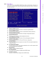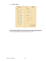
1
User Manual
PCM-4373
Copyright
The documentation and the software included with this product are copyrighted 2008
by Advantech Co., Ltd. All rights are reserved. Advantech Co., Ltd. reserves the right
to make improvements in the products described in this manual at any time without
notice. No part of this manual may be reproduced, copied, translated or transmitted
in any form or by any means without the prior written permission of Advantech Co.,
Ltd. Information provided in this manual is intended to be accurate and reliable. However, Advantech Co., Ltd. assumes no responsibility for its use, nor for any infringements of the rights of third parties, which may result from its use.
Acknowledgements
Award is a trademark of Award Software International, Inc.
VIA is a trademark of VIA Technologies, Inc.
IBM, PC/AT, PS/2 and VGA are trademarks of International Business
Machines Corporation.
Intel and Pentium are trademarks of Intel Corporation.
Microsoft Windows® is a registered trademark of Microsoft Corp.
RTL is a trademark of Realtek Semi-Conductor Co., Ltd.
ESS is a trademark of ESS Technology, Inc.
UMC is a trademark of United Microelectronics Corporation.
SMI is a trademark of Silicon Motion, Inc.
Creative is a trademark of Creative Technology LTD.
CHRONTEL is a trademark of Chrontel Inc.
All other product names or trademarks are properties of their respective owners.
PCM-4373 User Manual
Part No. 2006437310
Edition 1
Printed in Taiwan
December 2008
ii
Product Warranty (2 years)
Advantech warrants to you, the original purchaser, that each of its products will be
free from defects in materials and workmanship for two years from the date of purchase.
This warranty does not apply to any products which have been repaired or altered by
persons other than repair personnel authorized by Advantech, or which have been
subject to misuse, abuse, accident or improper installation. Advantech assumes no
liability under the terms of this warranty as a consequence of such events.
Because of Advantech’s high quality-control standards and rigorous testing, most of
our customers never need to use our repair service. If an Advantech product is defective, it will be repaired or replaced at no charge during the warranty period. For outof-warranty repairs, you will be billed according to the cost of replacement materials,
service time and freight. Please consult your dealer for more details.
If you think you have a defective product, follow these steps:
1. Collect all the information about the problem encountered. (For example, CPU
speed, Advantech products used, other hardware and software used, etc.) Note
anything abnormal and list any onscreen messages you get when the problem
occurs.
2. Call your dealer and describe the problem. Please have your manual, product,
and any helpful information readily available.
3. If your product is diagnosed as defective, obtain an RMA (return merchandise
authorization) number from your dealer. This allows us to process your return
more quickly.
4. Carefully pack the defective product, a fully-completed Repair and Replacement
Order Card and a photocopy proof of purchase date (such as your sales receipt)
in a shippable container. A product returned without proof of the purchase date
is not eligible for warranty service.
5. Write the RMA number visibly on the outside of the package and ship it prepaid
to your dealer.
Declaration of Conformity
FCC Class A
Note: This equipment has been tested and found to comply with the limits for a Class
A digital device, pursuant to part 15 of the FCC Rules. These limits are designed to
provide reasonable protection against harmful interference when the equipment is
operated in a commercial environment. This equipment generates, uses, and can
radiate radio frequency energy and, if not installed and used in accordance with the
instruction manual, may cause harmful interference to radio communications. Operation of this equipment in a residential area is likely to cause harmful interference in
which case the user will be required to correct the interference at his own expense.
iii
PCM-4373 User Manual
Technical Support and Assistance
1.
2.
Visit the Advantech web site at www.advantech.com/support where you can find
the latest information about the product.
Contact your distributor, sales representative, or Advantech's customer service
center for technical support if you need additional assistance. Please have the
following information ready before you call:
– Product name and serial number
– Description of your peripheral attachments
– Description of your software (operating system, version, application software,
etc.)
– A complete description of the problem
– The exact wording of any error messages
Packing List
Before setting up the system, check that the items listed below are included and in
good condition. If any item does not accord with the table, please contact your dealer
immediately.
! 1 x PCM-4373 SBC
! 1 x Startup manual
! 1 x Utility CD
! 1 x mini jumper pack (PN: 9689000002)
! 1 x CABLE USB*2/10-2.0 mm 29 cm (PN: 1700001267)
! 1 x FLAT Cable 50P 20 cm 3Com & LPT 1.27 mm to D-sub (PN: 1700002034)
! 1 x Cable 20P/10P EPIC ATX POWER 10 cm (PN: 1700002055)
! 1 x Cable 2*4P/10P EPIC AT POWER 15 cm (PN: 1700003931)
! 1 x CABLE 6P-6P-6P 20 cm PS/2 KB & MOUSE 20cm (PN: 1700060202)
! 2 x CABLE SERIAL ATA 7P/7P 30 cm (PN: 1700008894)
! 1 x Audio Cable IDC-10P 2.0 mm 15 cm (PN: 1700008902)
Ordering Information
PCM-4373L-J0A1E
AMD GX3 w/ 1 LAN/LVDS/0 GPIO /4 COM/4 USB/2 SATA,
AMD Lx800 chipset, 128 KB L2 cache, 1 x 10/100 LAN, 24 bit TTL, 1 x VGA, 4 x
USB2.0, 2 x RS-232, 2 x RS-232/422/485, 1 x LPT, 1 x CF, 2 x SATA, 1 x PC/104
Plus (0 ~ 60° C), passive thermal solution
PCM-4373F-J0A1E
Base PCM-4373L-J0A1E,w/2 LAN/16 GPIO/6 COM/Audio
AMD Lx800 chipset, 128 KB L2 cache, 2 x 10/100 LAN, 18 bit LVDS, 1 x VGA, 4 x
USB2.0, 4 x RS-232, 2 x RS-232/422/485, 16 bit GPIO, 1 x LPT, 1 x CF, 2 x SATA,
Audio, 1 x PC/104 Plus (0 ~ 60° C), passive thermal solution
Optional Accessories
1701200220 Cable for 2COM ports 20P 22 cm
1703150102 Wire BIG4P/Series ATA power 15P 10 cm module
1703040157 Wire RS-422/485 4P to D-SUB 15 cm
PCM-4373 User Manual
iv
Contents
Chapter
Chapter
1
General Introduction ...........................1
1.1
1.2
1.3
Introduction ............................................................................................... 2
Specifications ............................................................................................ 2
Chipset ...................................................................................................... 3
1.3.1 Functional Specification ................................................................ 3
1.3.2 Mechanical Specification .............................................................. 6
1.3.3 Electrical Specification .................................................................. 7
1.3.4 Environmental Specification.......................................................... 8
2
H/W installation....................................9
2.1
2.3
Jumpers .................................................................................................. 10
2.1.1 Jumper List ................................................................................. 10
2.1.2 Jumper Settings .......................................................................... 10
2.1.3 Jumper Description ..................................................................... 12
Connectors.............................................................................................. 13
2.2.1 Connector List............................................................................. 13
2.2.2 Connector Settings ..................................................................... 14
Mechanical .............................................................................................. 33
2.3.1 Jumper and Connector Locations ............................................... 33
Figure 2.1 PCM-4373 board layout (Component Side) ............. 33
Figure 2.2 PCM-4373 board layout (Solder Side)...................... 33
2.3.2 Board Dimensions....................................................................... 34
Figure 2.3 Board dimension layout (Component side) .............. 34
Figure 2.4 Board dimension layout (Solder side)....................... 35
Figure 2.5 Coast line layout ....................................................... 36
3
BIOS Operation ..................................37
3.1
3.2
BIOS Introduction.................................................................................... 38
BIOS Setup ............................................................................................. 38
3.2.1 Main Menu .................................................................................. 39
3.2.2 Standard CMOS Features .......................................................... 40
3.2.3 Advanced BIOS Features ........................................................... 41
3.2.4 Advanced Chipset Features........................................................ 42
3.2.5 Integrated Peripherals................................................................. 44
3.2.6 Power Management Setup ......................................................... 46
3.2.7 PnP/PCI Configurations .............................................................. 48
3.2.8 PC Health Status ........................................................................ 49
3.2.9 Load Optimized Defaults............................................................. 50
3.2.10 Set Password.............................................................................. 50
3.2.11 Save & Exit Setup ....................................................................... 52
3.2.12 Quit Without Saving .................................................................... 52
4
S/W Installation.................................53
4.1
4.2
S/W Introduction...................................................................................... 54
Driver Installation .................................................................................... 54
4.2.1 Windows XP Professional........................................................... 54
4.2.2 Other OS..................................................................................... 54
SUSI Application Library ......................................................................... 55
4.3.1 SUSI Introduction........................................................................ 55
2.2
Chapter
Chapter
4.3
v
PCM-4373 User Manual
4.3.2
4.3.3
4.3.4
Chapter
SUSI Functions........................................................................... 55
SUSI Installation ......................................................................... 56
SUSI Sample Programs.............................................................. 58
5
Extension I/O Installation ................. 67
5.1
SODIMM ................................................................................................. 68
Figure 5.1 SODIMM................................................................... 68
PC-104 Plus............................................................................................ 68
Figure 5.2 PC-104 Plus ............................................................. 68
5.2
Appendix A
Programming the GPIO & Watchdog
Timer69
A.1
A.2
Programming the Watchdog Timer ........................................................ 70
GPIO Sample Code ................................................................................ 71
Appendix B
System Assignments........................ 83
B.1
System I/O Ports..................................................................................... 84
Table B.1: System I/O Ports ...................................................... 84
1st MB memory map............................................................................... 85
Table B.2: 1st MB Memory Map ................................................ 85
DMA Channel Assignments .................................................................... 85
Table B.3: DMA Channel Assignments ..................................... 85
Interrupt Assignments ............................................................................. 86
Table B.4: Interrupt Assignments .............................................. 86
B.2
B.3
B.4
Appendix C
2nd RTC ............................................. 87
C.1
2nd RTC.................................................................................................. 88
PCM-4373 User Manual
vi
Chapter
1
1
General Introduction
This chapter gives background
information on PCM-4373.
Sections include:
! Introduction
! Specifications
1.1 Introduction
!
EPIC form factor (115 mm x 165 mm)
!
!
!
!
!
!
!
!
!
AMD GeodeTM LX800 processor, up to 500 MHz
Total system power consumption under 10W.
Up to 1 GB DDR SDRAM (supports FSB 266/333/400 MHz),1 x 200-pin
Display Combination: CRT+ 18 bit LVDS or CRT+ 24bit TTL
Dual 10/100 Mbps Ethernet
Supports ATX/ AT power modes (5 V only bootup)
Supports 1 x PC/104 Plus (PCI +16 bit ISA)
Supports 4 x USB 2.0, 2 x SATA
Supports 6 x COM (4 x RS232, 2 x RS232/422/485) or 4 x COM (2 x RS232,
2 x RS232/422/485)
Optional 16-bit GPIO and AC97 audio supported (PCM-4373F-J0A1E)
!
1.2 Specifications
General
! CPU: AMD Geode™ LX800 processor, up to 500 MHz
! 2nd Cache Memory: 128 KB
! System Chipset: AMD Geode™ LX800 + CS5536
! BIOS: Award 4Mb LPC BIOS
! System Memory: 1 x 200-pin SODIMM DDR FSB 266/333/400, up to 4GB
! Power Management: APM1.2, ACPI support
! Watchdog Timer: 255-level interval timer, setup by software, Super I/O integrated, SMSC Controller
! Expansion Interface: Supports 1 x PC/104 Plus (PCI +16 bit ISA)
! Battery: Lithium 3 V / 196 mAH
PCM-4373 User Manual
2
1.3.1 Functional Specification
1.3.1.1 Processor
!
!
!
Supports AMD GeodeTM LX800 processor, up to 500 MHz
128 KB L2 cache
Supports DDR 266, 333 and 400 MHz
North Bridge
Controller Hub
Display
AMD Geode LX800
VGA
TTL (24 bit)
LVDS (18 bit)
Choose National Semiconductor DS90CF363B (Advantech P/
N#1410000626)) for 18bit single channel LVDS
TTL and LVDS can display using same BIOS
Features
CRT resolutions supported:
Supports up to 1920x1440x32 bpp at 85 Hz
Supports up to 1600x1200x32 bpp at 100 Hz
LVDS resolutions supported:
Supports VGA, SVGA, XGA and Dual Pixel SXGA.
TTL supported:
Standard Definition (SD) resolution for Video Output Port (VOP):
720 x 482 at 59.94 Hz interlaced for NTSC
768 x 576 at 50 Hz interlaced for PAL
High Definition (HD) resolution for Video Output Port (VOP):
Up to 1920 x 1080 at 30 Hz interlaced (1080i HD) (74.25 MHz)
Up to 1280 x 720 at 60 Hz progressive (720p HD) (74.25 MHz)
Supports down to 7.652 MHz Dot Clock (320 x 240 QVGA)
Hardware supported 48 x 64 32-bit cursor with alpha blending
PCI Compliant
PCI 2.2 compliant
3.3 V signaling and 3.3 V I/Os
33 MHz operation
32-bit interface
Supports virtual PCI headers for GeodeLink devices
Security Block
Serial EEPROM interface for 2K bit unique ID and AES
(Advanced Encryption Standard) hidden key storage
(EEPROM optional inside package)
Electronic Code Book (ECB) or Cipher Block Chaining
(CBC)128-bit AES hardware support
True random number generator (TRNG)
3
PCM-4373 User Manual
General Introduction
1.3.1.2 Chipset (LX800)
Chapter 1
1.3 Chipset
1.3.1.3 Chipset (CS5536)
South Bridge
Controller Hub
AMD CS5536
Package
208-Terminal PBGA (plastic ball grid array) package
with internal heatspreader
AMD Geode CS5536 supports.
GeodeLink PCI Interface
(South Bridge)
Provides a PCI interface for GeodeLink Devices:
— PCI specification v2.2 compliant
— 32-Bit, 33 MHz operation
— Capable of handling in-bound transactions immediately
after reset - no setup
— Mapping of PCI virtual configuration space to MSR space is
done completely in Virtual System Architecture (VSA) code
— Serialized processor control interface
AMD Geode CS5536 supports.
LPC (Low Pin Count)
Interface
— Based on Intel LPC Interface specification v1.0
— Serial IRQ support
— Serial DMA support (8-bit only)
— Boot source typically off external LPC
— Supports firmware hub protocol
— External bus masters not supported
PCI Bus
PCI masters
10/100 LAN1 (RTL8100CL-LF)
10/100 LAN2 (RTL8100CL-LF)
Other Feature
4 USB 2.0 ports
2 Serial ATA (150MB/s) (Not support RAID function)
Power Management
LPC interface to Flash BIOS
6 COM ports, 4 x COM: RS-232; 2 x COM : RS-232/422/485
Signal (Support Auto flow control)
(Support via SMSC 3114 + Fintek 81216DG)
(Limitation: Under CE can support 6 COM ports but need to
choose close one IRQ device)
PCM-4373 User Manual
4
Chapter 1
1.3.1.4 Others (Chipset)
Display
Chipset
AMD Geode LX800
Dual independent display
NA
AMD Geode LX800 supports.
Supports video scaling, mixing and VOP
Graphics/video alpha blending and color key muxing
Digital VOP (SD and HD) or TFT outputs
VESA 1.1, 2.0 and BT.601 24-bit (out only), BT.656 compliant
Integrated Dot Clock PLL with up to 350 MHz clock
Integrated 3 x 8-bit DAC with up to 350 MHz sampling
Analog CRT DAC interface support
VGA
CRT resolutions supported:
Supports up to 1920 x 1440 x 32 bpp at 85 Hz
Supports up to 1600 x 1200 x 32 bpp at 100 Hz
LVDS
18-bit (convert from TTL via NS DS90CF363B)
18 to 68 MHz shift clock support
Supports VGA, SVGA, XGA and Dual Pixel SXGA.
Compatible with TIA/EIA-644 LVDS standard
TTL
It supports panels up to a 24-bit interface and up to
1600 x 1200 resolution.
Internal Graphics
Features
2D Graphics Processor
High performance 2D graphics controller
Alpha BLT
Microsoft Windows GDI GUI acceleration:
— Hardware support for all Microsoft RDP codes
Command buffer interface for asynchronous BLTs
Second pattern channel support
Hardware screen rotation
New features added to the Graphics Processor include:
Command buffer interface
Hardware accelerated rotation BLTs
Color depth conversion
Paletized color
Full 8x8 color pattern buffer
Separate base addresses for all channels
Monochrome inversion
LAN
Chipset
LAN 1 / LAN 2: Realtek RTL8100CL-LF
IEEE Compliant
full compliance with IEEE 802.3 u 100BASE-T and IEEE 802.3
x full duplex flow control.
32-bit PCI Ethernet controller.
LAN LED
LED1: Green for 10M/100M LAN
LED2: Off for Link, flash for active,
Disable LAN through BIOS Yes
Wake on LAN
Yes
Boot from LAN
Yes
LED connector
Yes
5
PCM-4373 User Manual
General Introduction
Video Processor & Integrated Analog Display
Audio
Chipset
AC97 Audio
Codec
ALC203
Rear panel output
Line-In, Line-out, Mic-In
Amplifier
NA
Hardware Monitor
Chipset
LPC I/O for onboard alarm
SMSC3114
Temperature
CPU Temperature
Voltage
2.5 V, Vcore, 12 V, 5 V
Super I/O
Chipset
SMSC3114
Fan speed monitor
Yes
Temperature
Yes
Features
LPC interface
4 full function serial ports
watch dog timer
Hardware Monitoring
– Thermal Sensing :2 external, 1 internal
– (7) Voltage Monitoring
Infrared port: IrDA 1.0 compliant
1.3.2 Mechanical Specification
1.3.2.1 Dimension (mm)
115 mm (L) x 165 mm (W) (4.5" x 6.5")
1.3.2.2 Height on Top (mm)
9.8 mm (Heatsink)
1.3.2.3 Height on Bottom (mm)
9.2 mm (SODIMM Socket)
1.3.2.4 Cooler Dimension (mm)
39.6 x 39.5 x 9.8 mm (Heatsink)
1.3.2.5 Weight (g) with Cooler
110 g
PCM-4373 User Manual
6
1.3.3.1 Power Supply Voltage
Power Type
Power
AT/ATX
ATX: +5 V ± 5%,+5 Vsb to work (±12 V ± 5% optional for
LCD inverter and add on card.)
Power Supply Voltage
AT: +5 V ± 5% (±12 V ± 5% optional for LCD inverter and
add on card.)
APM, ACPI
Battery
Lithium 3 V/196 mAH
General Introduction
Power Management
1.3.3.2 Power Supply Current
Test Conditions
:
OS - WindowsXP SP2
Add-in Card - None
CF Card - None
MiniPCI Card - None
HDD - 160GB SATA *1
BIOS - 4373V111.bin
KeyBoard/Mouse - USB or PS/2 Interface
Display - CRT
Memory 512MB
Apacer DDR 400 64MB X 8
ATX
CPU
AMD LX800
Status
+V5
+V12
+V5SB
0.02 A
BIOS Picture
1.52 A
Unused
0.02 A
DOS Idle
1.50 A
Unused
0.02 A
Win Idle
1.45 A
Unused
0.02 A
Win HCT12.0
1.72
Unused
0.02 A
+V5 maximum current: 1.85 A
AT
CPU
AMD LX800
+V5
+V12
BIOS Picture
1.52 A
Unused
DOS Idle
1.50 A
Unused
Win Idle
1.45 A
Unused
Win HCT12.0
1.72
Unused
Status
+V5 maximum current: 1.9 A
1.3.3.3 RTC Battery
! Typical Voltage: 3.0 V
! Normal discharge capacity: 196 mAh3
7
Chapter 1
1.3.3 Electrical Specification
PCM-4373 User Manual
1.3.4 Environmental Specification
1.3.4.1 Operating Temperature
The AMD® CPU LX800 is specified for proper operation temperature range of 40° C
~ +85° C.
The AMD CS5536 I/O Controller case temperature runs at a maximum of 95° C.
Operating temperature: 0 ~ 60° C (32 ~ 140° F)
1.3.4.2 Operating Humidity
Operating humidity: 0% ~ 90% relative humidity, non-condensing
1.3.4.3 Storage Temperature
Standard products (0 ~ 60° C)
Storage temperature: -20 ~ 70° C
1.3.4.4 Storage Relative Humidity
Standard products (0 ~ 60° C)
Relative humidity: 95% @ 60° C
Phoenix products (-20 ~ 80° C)
Relative humidity: 95% @ 60° C
Platinum Phoenix products (-40 ~ 85° C)
Relative humidity: 95% @ 60° C
PCM-4373 User Manual
8
Chapter
2
2
H/W installation
This chapter explains the setup
procedures of the PCM-4373 hardware, including instructions on
setting jumpers and connecting
peripherals, switches, indicators
and mechanical drawings.Be sure
to read all safety precautions
before you begin the installation
procedure.
Sections include:
! Jumpers
! Connectors
! Mechanical
2.1 Jumpers
2.1.1 Jumper List
J1
AT Select
J2
DOTREF Select
J3
LVDS POWER Select
J4
CMOS Clear
J5
COM1 Mode Select
J6
COM2 Mode Select
J7
PCI VIO Select
J9
IrDA/COM2 Select
2.1.2 Jumper Settings
J1
AT select
Part Number
1653002101
Footprint
JH2X1V-2M
Description
PIN HEADER 2*1P 180D (M) 2.0 mm DIP SQUARE W/O Pb
Setting
Function
(1-2)
AT Enable
J2
DOTREF Select
Part Number
1653002101
Footprint
JH2X1V-2M
Description
PIN HEADER 2*1P 180D (M) 2.0 mm DIP SQUARE W/O Pb
Setting
Function
(1-2)
External
NL
Internal
J3
LVDS Power Select
Part Number
1653003101
Footprint
JH3X1V-2M
Description
PIN HEADER 3*1P 180D (M) 2.0 mm DIP SQUARE W/O Pb
Setting
Function
(1-2)
5V
(2-3)
3.3 V (Default)
PCM-4373 User Manual
10
1653003101
Footprint
JH3X1V-2M
Description
PIN HEADER 3*1P 180D (M) 2.0 mm DIP SQUARE W/O Pb
Setting
Function
(1-2)
Disable (Default)
(2-3)
Clear
J5
COM1 Mode Select
Part Number
1653003260
Footprint
JH3X2S-2M
Description
PIN HEADER 3*2P 180D (M) 2.0 mm DIP SQUARE W/O Pb
Setting
Function
(1-2)
232 (Default)
(3-4)
485
(5-6)
422
J6
COM2 Mode Select
Part Number
1653003260
Footprint
JH3X2S-2M
Description
PIN HEADER 3*2P 180D (M) 2.0 mm DIP SQUARE W/O Pb
Setting
Function
(1-2)
232 (Default)
(3-4)
485
(5-6)
422
NL
IrDA
J7
PCI VIO Select
Part Number
1653003101
Footprint
JH3X1V-2M
Description
PIN HEADER 3*1P 180D (M) 2.0 mm DIP SQUARE W/O Pb
Setting
Function
(1-2)
5 V (Default)
(2-3)
3.3 V
J9
IrDA/COM2 Select
Part Number
1653002101
Footprint
JH3X1V-2M
Description
PIN HEADER 3*1P 180D (M) 2.0 mm DIP SQUARE W/O Pb
Setting
Function
(1-2)
COM2
NL
IrDA
11
PCM-4373 User Manual
H/W installation
CMOS Clear
Part Number
Chapter 2
J4
2.1.3 Jumper Description
Cards can be configured by setting jumpers. A jumper is a metal bridge used to close
an electric circuit. It consists of two metal pins and a small metal clip (often protected
by a plastic cover) that slides over the pins to connect them. To close a jumper, you
connect the pins with the clip. To open a jumper, you remove the clip. Sometimes a
jumper will have three pins, labeled 1, 2 and 3. In this case you would connect either
pins 1 and 2, or 2 and 3.
The jumper settings are schematically depicted in this manual as follows.
Warning! To avoid damaging the computer, always turn off the power supply
before setting jumpers. Clear CMOS. Before turning on the power supply, set the jumper back to 3.0 V Battery On.
PCM-4373 User Manual
12
Chapter 2
2.2 Connectors
2.2.1 Connector List
POWER connector
CN3
DDR SO-DIMM
CN5
FAN connector
CN7
GPIO1 connector
CN8
LAN1(RJ45)
CN9
LAN2(RJ45)
CN11
Compact Flash connector
CN13
HD & Power LED
CN14
Internal LVDS connector
CN16
CRT connector
CN18
USB0/1
CN19
KB/MS connector
CN20
USB2/3
CN21
COM1
CN22
AUDIO connector
CN25
PCI-104 connector
CN26
COM1 RS422/485 connector
CN30
COM2/3/4 & LPT
CN32
SATA1 connector
CN33
SATA2 connector
CN36
TTL LCD connector
CN37
SMBUS Connector
CN38
Panel Inverter Power
CN39
ATX POWER Button
CN41
COM5,6
CN43
COM2 RS422/485 connector
CN44
ISA -V5 Connector
CN46
GPIO2 Connector
CN53
BATTERY connector
CN54
IrDA Connector
13
H/W installation
CN1
PCM-4373 User Manual
2.2.2 Connector Settings
CN1: Power connectors
Main power connector, +3.3 V, +5 V, +12 V, -12 V
PCM-4373 can support both ATX and AT power supply and it can use different power
cable to do the choice.
1. ATX power supply: you need to use ATX power cable (PN: 1700002055 Cable
20P/10P EPIC ATX POWER 10CM)
2. AT power supply: you need to use AT power cable (PN: 1700003931 AT Power
Cable 2*4P/10P EPIC AT POWER 15cm)
CN1 connector is 10-Pin power connector and it allows you to connect to an ATX or
AT power supply by different power cable.
CN1
Power Connector
Part Number
1655000042
Footprint
ATXCON-2X5-42-1
Description
WAFER 4.2 mm 10P 180D(M) DIP 4200-WS-A1-2*5
Pin
Pin Name
Signal Type
Signal Level
1
SIO_PSON#
IN
+5 V
2
GND
3
GND
4
+V12
PWR
+12 V
5
NC
PWR
+3.3 V
6
+V5SB_ATX
PWR
+5 V
7
+V5
PWR
+5 V
8
+V5
PWR
+5 V
9
-V12
PWR
-12 V
10
GND
PCM-4373 User Manual
14
DDR SO-DIMM
Part Number
1651000705
Footprint
SODIMM_200P_ASOA426-EASN-4F
Description
SKT DDR2-SODIMM 200P H=9.2 SMD AS0A426-NASN-7F
CN5: Fan connector
Provides power supply +5 V for CPU cooling fan, and fan speed detects signal input.
CN5
FAN connector
Part Number
1655303020
Footprint
WHL3V-2M
Description
Wafer 2.00mm 3P 180D(M) DIP W/LOCK 22-27-2031
Pin
Pin Name
Signal Type
1
FAN0_IO
OUT
2
+V5
PWR
3
GND
15
Signal Level
+5 V
PCM-4373 User Manual
H/W installation
CN3
Chapter 2
CN3: DDR2 SO-DIMM
A SO-DIMM, or small outline dual in-line memory module, is a type of computer
memory built using integrated circuits.PCM-4373 has 1 x 200 pin SO-DIMM and can
support memory size up to 1 GB.
CN7: GPIO1 (General Purpose Input Output)
PCM4373 supports 16-bit GPIO via CN7 and CN46.
CN7
GPIO1 connector
Part Number
1653000383
Footprint
JH5X2S-2M21N22050
Description
PIN HEADER 5*2P 90D(M) 2.0 mm SMD WO/Pb
Pin
Pin Name
Signal Type
Signal Level
1
+5 V
PWR
+5 V
2
GPIO4
I/O
+5 V
3
GPIO0
I/O
+5 V
4
GPIO5
I/O
+5 V
5
GPIO1
I/O
+5 V
6
GPIO6
I/O
+5 V
7
GPIO2
I/O
+5 V
8
GPIO7
I/O
+5 V
9
GPIO3
I/O
+5 V
10
GND
CN8: Ethernet connector
The board is equipped with 2 high performance Ethernet interface which use RJ45
connector. One is CN8 and another one is CN9.
CN8
LAN1(RJ45+1G Transformer)
Part Number
1652000147
Footprint
RJ45X10-LED-1AX9
Description
Phone Jack RJ45 14P 90D (F) W/Xfam P26@P07-1AM9
Pin
Pin Name
Signal Type
Signal Level
1
LAN1_TX+
OUT
Analog
2
LAN1_TX-
OUT
Analog
3
LAN1_RX+
IN
Analog
4
LAN1_RX-
IN
Analog
5
+V3.3_LAN1
PWR
6
NC
7
NC
8
NC
PCM-4373 User Manual
16
Chapter 2
CN9: Ethernet Connector
CN9
LAN2(RJ45+1G
Transformer)
Part Number
1652000174
Footprint
RJ45+XFMR+LED
Description
Phone Jack RJ45 14P 90D (F) W/Xfam P26@P07-1AM9
Pin
Pin Name
1
LAN2_TX+
OUT
Analog
2
LAN2_TX-
OUT
Analog
3
LAN2_RX+
IN
Analog
4
LAN2_RX-
IN
Analog
5
+V3.3_LAN2
PWR
6
NC
7
NC
8
NC
Signal Type
Signal Level
CN11: Compact Flash connector
The board provides a CompactFlash. card type I/II socket and the CompactFlash use
master IDE channel.
CN11
Compact Flash connector
Part Number
1653002086
Footprint
SPEED_N016-0140104
Description
CF HEADER 50P 90D (M) 1.27 mm SMD Type2 Standoff=2
17
PCM-4373 User Manual
H/W installation
The board is equipped with 2 high performance Ethernet interface which use RJ45
connector. One is CN9 and another one is CN8.
CN13: HD and Power LED
1
2
3
4
CN13 is an indication LED connector for HD and power.
CN13
HD & Power LED
Part Number
1653004101
Footprint
JH4X1V-2M
Description
PIN HEADER 4*1P 180D (M) SQUARE 2.0 mm
Pin
Pin Name
Signal Type
Signal Level
1
+VCC_1
PWR
+5 V
2
GND
3
+VCC_2
PWR
+5 V
4
HD_LED
OUT
+5 V
CN14: LVDS connector
CN14 is LVDS (Low Voltage Differential Signal) connector. You can connect to 18 bit
LVDS LCD panel via CN14.
CN14
Internal LVDS Connector
Part Number
1653910261
Footprint
SPH10X2
Description
*CONN. 20P 90D 1.25 mm SMD WO/Pb DF13-40DP-1.25 V
Pin
Pin Name
1
GND
2
GND
3
LVDS0_D0+
4
NC
5
LVDS0_D0-
6
NC
7
LVDS0_D1+
8
NC
9
LVDS0_D1-
10
NC
11
LVDS0_D2+
12
NC
13
LVDS0_D2-
14
NC
15
LVDS0_CLK+
16
NC
17
LVDS0_CLK-
Signal Type
Signal Level
OUT
LVDS
OUT
LVDS
OUT
LVDS
OUT
LVDS
OUT
LVDS
OUT
LVDS
OUT
LVDS
OUT
LVDS
18
NC
19
VCC_LVDSB
PWR
+5 V/+3.3 V
20
VCC_LVDSA
PWR
+5 V/+3.3 V
PCM-4373 User Manual
18
Chapter 2
CN16: VGA connector
The DB15-pin female connector is provided for video monitors.
CRT Connector
Part Number
1654000055
Footprint
DBVGA-VF5MS
Description
D-SUB Conn. 15P 90D (F) DIP 070242FR015S200ZU
Pin
Pin Name
Signal Type
Signal Level
1
VGA_z_R
OUT
Analog
2
VGA_z_G
OUT
Analog
3
VGA_z_B
OUT
Analog
4
NC
5
GND
GND
6
GND
GND
7
GND
GND
8
GND
GND
9
+V5_b_VGA
PWR
10
GND
GND
11
NC
12
VGA_y_DDAT
OUT
+5 V
13
VGA_y_HS
OUT
+5 V
14
VGA_y_VS
OUT
+5 V
15
VGA_y_DCLK
OUT
+5 V
19
+5 V
PCM-4373 User Manual
H/W installation
CN16
CN18: USB connectors
The board provides up to 4 x USB (Universal Serial Bus) ports. You can use it by
CN18 and CN20. CN18 is a 2 x USB type A connector and CN20 is a pin header
type. PCM-4373 USB ports gives complete Plug and Play, and hot attach/detach for
up to 127 external devices and comply with USB specification Rev. 2.0 which supports 480Mbps transfer rate, and are fuse protected.
CN18
USB0/1
Part Number
1654908100
Footprint
USBX2-V
Description
USB Conn. DUAL port 8P 90D (M) Black PC99
Pin
Pin Name
Signal Type
Signal Level
1
+V5DUAL_USB0
PWR
+5 V
2
USB0_z_P-
I/O
3
USB0_z_P+
I/O
4
GND
5
+V5DUAL_USB0
PWR
6
USB1_z_P-
I/O
7
USB1_z_P+
I/O
8
GND
9
GND
10
GND
11
GND
12
GND
PCM-4373 User Manual
20
+5 V
This connector is for PS/2 keyboard and mouse. You need a one to two connector
cable (Part number: 1700060202) for keyboard and mouse.
KB/MS Connector
Part Number
1654003199
Footprint
CONTEK_MQN3261F
1G400
Description
MINIDIN 6P Short body W/Shielding90D (F) DIP
Pin
Pin Name
Signal Type
Signal Level
1
KB_z_DAT#
I/O
+5 V
2
MS_z_DAT#
I/O
+5 V
3
GND
4
+V5DUAL_PS2
PWR
+5 V
5
KB_z_CLK#
I/O
+5 V
6
MS_z_CLK#
I/O
+5 V
CN20: USB connectors
CN20 is a pin header type for 2 x USB 2.0 ports. PCM-4373 USB ports gives complete Plug and Play, and hot attach/detach for up to 127 external devices and comply
with USB specification Rev. 2.0 which supports 480Mbps transfer rate, and are fuse
protected.
CN20
USB2/3
Part Number
1653205261
Footprint
HD_5x2P_79_BOX_N
10
Description
PIN HEADER 5x2P 180D (M) 2.0 mm SMD IDIOT-PROOF
Pin
Pin Name
Signal Type
Signal Level
1
+V5DUAL_USB1
PWR
+5 V
2
+V5DUAL_USB1
PWR
+5 V
3
USB2_z_P-
I/O
4
USB3_z_P-
I/O
5
USB2_z_P+
I/O
6
USB3_z_P+
I/O
7
GND
8
GND
9
GND
21
PCM-4373 User Manual
H/W installation
CN19
Chapter 2
CN19: Keyboard and PS/2 mouse connector
CN21: COM1 port connector for RS232
PCM-4373 provides 6 serial communication ports. CN21 is one of the serial communication ports. CN21 is 9 pin D-shell connector used for the RS 232 serial port.
CN21
COM1
Part Number
1654000056
Footprint
DBCOM-VM5MS
Description
D-SUB CON. 9P 90D (M) DIP 070241MR009S200ZU SUYIN
Pin
Pin Name
Signal Type
Signal Level
1
COM0_z_DCD#
IN
+5 V
2
COM0_z_RXD
IN
+5 V
3
COM0_z_TXD
OUT
+5 V
4
COM0_z_DTR#
I/O
+5 V
5
GND
6
COM0_z_DSR#
IN
+5 V
7
COM0_z_RTS#
I/O
+5 V
8
COM0_z_CTS#
IN
+5 V
9
COM0_z_RI
IN
+5 V
CN22: Audio interface
Audio Port Connectors
CN27 is a 5 x 2P box header and it is for audio interface.
CN22
AUDIO connector
Part Number
1653205260
Footprint
BH5x2P-S2.00
Description
BOX HEADER SMD 5*2 180D (M) 2.0 mm
Pin
Pin Name
Signal Type
Signal Level
1
LINEOUT_R
Out
Analog
2
LINEIN_R
IN
Analog
3
AGND
GND
4
AGND
GND
5
LINEOUT_L
Out
Analog
6
LINEIN_L
IN
Analog
7
AGND
GND
PCM-4373 User Manual
22
AGND
9
NC
10
MIC1_L
GND
IN
Analog
CN25: PCI-104 connector
CN25 is a PCI104 connector. PCI-104 form factor includes the PCI connector. It is
intended for industrial embedded computing environments where applications
depend on reliable data acquisition.
PCI-104 Connector
Part Number
1653130428
Footprint
PC104-PCI-PLUS
Description
PCB SKT 30*4 180D (F)PC/104+ SOLDER WO/Pb EPT
CN26: COM1 for RS422/485
CN26 is a 1 x 4P connector for RS422/485.
CN26
COM1 RS-422/485
connector
Part Number
1653004101
Footprint
JH4X1V-2M
Description
PIN HEADER 4*1P 180D (M) SQUARE 2.0 mm
Pin
Pin Name
Signal Type
Signal Level
1
RS422_RXD-
IN
+5 V
2
RS422_RXD+
IN
+5 V
3
RS485-422_TXD+
OUT
+5 V
4
RS485-422_TXD-
OUT
+5 V
23
PCM-4373 User Manual
H/W installation
CN25
Chapter 2
8
CN30: COM port connector
CN30 is a connector and includes COM2, COM3, COM4 and LPT signal. You can
use a one to four connector cable (PN:1700002034) to connect to your device. CN30
is a 2 x 25P box header.
49
1
50
2
CN30
Part Number
Footprint
Description
COM2/3/4 & LPT
1653001605
BH_25x2P_50_BOX_LOCK
BOX HEADER 25*2P 180D (M) 1.27 mm SMD CEN LINK
Pin
Pin Name
Signal Type
Signal Level
1
COM1_DCD#
IN
+5 V
2
COM1_DSR#
IN
+5 V
3
COM1_RXD
IN
+5 V
4
COM1_RTS#
I/O
+5 V
5
COM1_TXD
OUT
+5 V
6
COM1_CTS#
IN
+5 V
7
COM1_DTR#
I/O
+5 V
8
COM1_RI#
IN
+5 V
9
GND
10
GND
11
COM2_DCD#
IN
+5 V
12
COM2_DSR#
IN
+5 V
13
COM2_RXD
IN
+5 V
14
COM2_RTS#
I/O
+5 V
15
COM2_TXD
OUT
+5 V
16
COM2_CTS#
IN
+5 V
17
COM2_DTR#
I/O
+5 V
18
COM2_RI#
IN
+5 V
19
GND
20
GND
21
COM3_DCD#
IN
+5 V
22
COM3_DSR#
IN
+5 V
23
COM3_RXD
IN
+5 V
24
COM3_RTS#
I/O
+5 V
25
COM3_TXD
OUT
+5 V
26
COM3_CTS#
IN
+5 V
27
COM3_DTR#
I/O
+5 V
28
COM3_RI#
IN
+5 V
29
GND
30
GND
31
LPT_z_STB#
OUT
+5 V
32
LPT_z_AFD#
OUT
+5 V
PCM-4373 User Manual
24
LPT_z_PRD0
I/O
+5 V
34
LPT_z_ERR#
IN
+5 V
35
LPT_z_PRD1
I/O
+5 V
36
LPT_z_INIT#
OUT
+5 V
37
LPT_z_PRD2
I/O
+5 V
38
LPT_z_SLIN#
OUT
+5 V
39
LPT_z_PRD3
I/O
+5 V
LPT_z_PRD4
I/O
+5 V
41
LPT_z_PRD5
I/O
+5 V
42
LPT_z_PRD6
I/O
+5 V
43
LPT_z_PRD7
I/O
+5 V
44
LPT_ACK#
IN
+5 V
45
LPT_BUSY
IN
+5 V
46
LPT_PE
IN
+5 V
47
LPT_SLCT
I/O
+5 V
48
GND
49
GND
50
GND
CN32: SATA Connector
PCM-4373 supports Serial ATA via two connectors (CN32 and CN33). Data transfer
rates up to 150 MB/s per channel, enabling very fast data and file transfer, and independent DMA operation on two ports.
CN32
SATA1 connector
Part Number
1654003639
Footprint
SATA_7P_01770655-1_D
Description
Serial ATA Con 7p 180D (M) DIP 1.27 mm 0-1770655-1
Pin
Pin Name
1
GND
GND
2
SATA0_TX+
I/O
Analog
3
SATA0_TX-
I/O
Analog
4
GND
GND
5
SATA0_RX-
I/O
Analog
6
SATA0_RX+
I/O
Analog
7
GND
GND
Signal Type
25
Signal Level
PCM-4373 User Manual
H/W installation
40
Chapter 2
33
CN33: SATA Connector
PCM-4373 supports Serial ATA via two connectors (CN32 and CN33). Data transfer
rates up to 150 MB/s per channel, enabling very fast data and file transfer, and independent DMA operation on two ports.
CN33
SATA2 connector
Part Number
1654003639
Footprint
SATA_7P_01770655-1_D
Description
Serial ATA Con 7p 180D (M) DIP 1.27 mm 0-1770655-1
Pin
Pin Name
Signal Type
1
GND
GND
2
SATA1_TX+
I/O
Analog
3
SATA1_TX-
I/O
Analog
4
GND
GND
5
SATA1_RX-
I/O
Analog
6
SATA1_RX+
I/O
Analog
7
GND
GND
Signal Level
CN36: TTL LCD connector
CN36 is TTL LCD connector. You can connect to 24bit TTL LCD panel via CN36.
CN36
TTL LCD Connector
Part Number
1653920200
Footprint
SPH20X2
Description
CONN. 40P 90D 1.25 mm SMD WO/Pb DF13-40DP-1.25 V
Pin
Pin Name
Signal Type
Signal Level
1
+5 V_LCD
+5 V
+5 V
2
+5 V_LCD
+5 V
+5 V
3
GND
4
GND
5
+3.3 V_LCD
+3.3 V
+3.3 V
6
+3.3 V_LCD
+3.3 V
+3.3 V
7
GND
8
GND
9
FP_D0 (Bo)
OUT
TTL
10
FP_D1 (B1)
OUT
TTL
PCM-4373 User Manual
26
OUT
TTL
12
FP_D3 (B3)
OUT
TTL
13
FP_D4 (B4)
OUT
TTL
14
FP_D5 (B5)
OUT
TTL
15
FP_D6 (B6)
OUT
TTL
16
FP_D7 (B7)
OUT
TTL
17
FP_D8 (G0)
OUT
TTL
18
FP_D9 (G1)
OUT
TTL
19
FP_D10 (G2)
OUT
TTL
20
FP_D11 (G3)
OUT
TTL
21
FP_D12 (G4)
OUT
TTL
22
FP_D13 (G5)
OUT
TTL
23
FP_D14 (G6)
OUT
TTL
24
FP_D15 (G7)
OUT
TTL
25
FP_D16 (R0)
OUT
TTL
26
FP_D17 (R1)
OUT
TTL
27
FP_D18 (R2)
OUT
TTL
28
FP_D19 (R3)
OUT
TTL
29
FP_D20 (R4)
OUT
TTL
30
FP_D21 (R5)
OUT
TTL
31
FP_D22 (R6)
OUT
TTL
32
FP_D23 (R7)
OUT
TTL
33
GND
OUT
TTL
34
GND
OUT
TTL
35
FP_CLK
OUT
+3.3 V
36
FP_VS
OUT
+3.3 V
37
FP_DE
OUT
+3.3 V
38
FP_HS
OUT
+3.3 V
39
PRST_LCD#
OUT
+3.3 V
40
FP_ENVEE
OUT
+3.3 V
CN37: Battery Connector
2
CN37 is for SMBUS connection. It is a pin header type and part number is
1653002101.
CN37
SMBUS Connector
Part Number
1653002101
Footprint
JH2X1V-2M
Description
Pin header BOX 2.0 mm 2P 180D MALE W/LOCK
Pin
Pin Name
Signal Type
Signal Level
1
SMB_CLK
Out
+3.3 V
2
SMB_DAT
I/O
+3.3 V
27
PCM-4373 User Manual
H/W installation
FP_D2 (B2)
Chapter 2
11
CN38: Panel Inverter Power
CN15 is a 5-pin connector. PCM-4373 can provide +5V and +12V and signal to LCD
inverter board by this connector.
CN38
Panel Inverter Power
Part Number
1655305020
Footprint
WHL5V-2M
Description
WAFER BOX 2.0 mm 5P 180D (M) W/LOCK
Pin
Pin Name
Signal Type
Signal Level
1
+V12_LCD
PWR
+12 V
2
GND
GND
3
FP_ENABKL
OUT
+3.3 V
4
FP_VBR
OD
+3.3 V
5
+V5
PWR
+5 V
CN39: ATX Power button connector
CN39 connects to power button to support to turn on/off PCM-4373. It is 2 pins wafer
type.
CN39
ATX Power Button
Part Number
1655302020
Footprint
WHL2V-2M
Description
WAFER BOX 2P 180D 2.0 mm MALE W/Lock
Pin
Pin Name
Signal Type
Signal Level
1
SB_PWRBTN#
IN
+3.3V
2
GND
GND
PCM-4373 User Manual
28
Chapter 2
CN41: COM port connector
CN41 is a 10 x 2P box header for COM5 and COM6.
COM5,6
Part Number
1653005261
Footprint
HD_10x2P_79_BOX
Description
PIN HEADER SMD 5*2P 180D (M) 2.0 mm
Pin
Pin Name
Signal Type
Signal Level
1
DCD#
IN
+5 V
2
DSR#
IN
+5 V
3
RXD#
IN
+5 V
4
RTS#
I/O
+5 V
5
TXD#
OUT
+5 V
6
CTS#
IN
+5 V
7
DTR#
I/O
+5 V
8
RI#
IN
+5 V
9
GND
10
GND
11
DCD#
IN
+5 V
12
DSR#
IN
+5 V
13
RXD#
IN
+5 V
14
RTS#
I/O
+5 V
15
TXD#
OUT
+5 V
16
CTS#
IN
+5 V
17
DTR#
I/O
+5 V
18
RI#
IN
+5 V
19
GND
20
GND
29
PCM-4373 User Manual
H/W installation
CN41
CN43: COM2 for RS422/485
CN43 is a 1 x 4P connector for RS422/485.
CN43
COM2 RS-422/485
connector
Part Number
1653004101
Footprint
JH4X1V-2M
Description
PIN HEADER 4*1P 180D (M) SQUARE 2.0 mm
Pin
Pin Name
Signal Type
Signal Level
1
RS422_RXD-
IN
+5 V
2
RS422_RXD+
IN
+5 V
3
RS485-422_TXD+
OUT
+5 V
4
RS485-422_TXD-
OUT
+5 V
CN44: ISA -5V power
CN44 connects is for ISA -5 V power.
CN44
ISA -5V POWER
Part Number
1653002101
Footprint
JH2X1V-2M
Description
PIN HEADER 2*1P 180D (M)SQUARE 2.00 mm
Pin
Pin Name
Signal Type
Signal Level
1
-V5
PWR
-5 V
2
GND
PCM-4373 User Manual
30
Chapter 2
CN46: GPIO1 (General Purpose Input Output)
PCM4373 supports 16-bit GPIO via CN7 and CN46.
GPIO2 connector
Part Number
1653000383
Footprint
JH5X2S-2M21N22050
Description
PIN HEADER 5*2P 90D (M) 2.0 mm SMD WO/Pb
Pin
Pin Name
Signal Type
Signal Level
1
+5 V
PWR
+5 V
2
GPIO12
I/O
+5 V
3
GPIO8
I/O
+5 V
4
GPIO13
I/O
+5 V
5
GPIO9
I/O
+5 V
6
GPIO14
I/O
+5 V
7
GPIO10
I/O
+5 V
8
GPIO15
I/O
+5 V
9
GPIO11
I/O
+5 V
10
GND
CN53: Battery Connector
CN53 is for battery connection. It is 2 pins wafer type and part number is
1655902032.
CN53
BATTERY connector
Part Number
1655902032
Footprint
WHL2V-125
Description
WAFER 2P 180D (M) 1.25 mm 53047-0210
Pin
Pin Name
Signal Type
Signal Level
1
+VBAT
PWR
+3.3 V
2
GND
GND
31
PCM-4373 User Manual
H/W installation
CN46
CN54: IrDA connector
CN54 is 5-pin connector for IrDA.
CN54
IrDA connector
Part Number
1653005101
Footprint
PH5x1P-2.00
Description
Pin Header 5P 180D (M) 2.00 mm
Pin
Pin Name
Signal Type
Signal Level
1
+V5_IrDA
PWR
+5 V
2
NC
3
RXD
IN
+5 V
4
GND
GND
5
TXD
OUT
PCM-4373 User Manual
32
+5 V
Chapter 2
2.3 Mechanical
2.3.1 Jumper and Connector Locations
H/W installation
TTL LCD
LVDS
Figure 2.1 PCM-4373 board layout (Component Side)
Figure 2.2 PCM-4373 board layout (Solder Side)
!
!
!
Dimension (mm): 115 mm (W) x 165 mm (L) (4.5" x 6.5")
Height on Top (mm): 17 mm (Including Heatsink)
Height on Bottom (mm): 9.2 mm (SODIMM Socket)
33
PCM-4373 User Manual
PCM-4373 User Manual
34
159.92 [6.296]
154.34 [6.076]
142.14 [5.596]
136.54 [5.375]
114.38 [4.503]
106.10 [4.177]
87.38 [3.440]
59.97 [2.361]
62.13 [2.446]
50.50 [1.988]
23.79 [0.937]
10.40 [0.409]
5.08 [0.200]
0.00 [0.000]
R
4.
00
[R
0.
15
7]
154.34 [6.076]
147.22 [5.796]
139.60 [5.496]
73.56 [2.896]
65.94 [2.596]
57.05 [2.246]
50.50 [1.988]
6.73 [0.265]
9.50 [0.374]
0.00 [0.000]
2.3.2 Board Dimensions
109.97 [4.330]
104.85 [4.128]
104.85 [4.128]
92.10 [3.626]
44.84 [1.765]
14.05 [0.553]
19.13 [0.753]
3.84 [0.151]
0.00 [0.000]
1.07 [0.042]
1.52 [0.060]
5.08 [0.200]
1.74 [0.068]
0.00 [0.000]
10.77 [0.424]
Figure 2.3 Board dimension layout (Component side)
[R
68.36 [2.691]
95.01 [3.741]
154.34 [6.076]
.0
0
0.
15
7]
109.97 [4.330]
104.85 [4.128]
104.85 [4.128]
Chapter 2
R4
94.13 [3.706]
85.79 [3.377]
0.00 [0.000]
5.08 [0.200]
154.34 [6.076]
159.92 [6.296]
117.96 [4.644]
Figure 2.4 Board dimension layout (Solder side)
35
PCM-4373 User Manual
H/W installation
0.00 [0.000]
5.08 [0.200]
0.00 [0.000]
Figure 2.5 Coast line layout
PCM-4373 User Manual
36
Chapter
3
BIOS Operation
Sections include:
! BIOS Introduction
! BIOS Setup
3
3.1 BIOS Introduction
Advantech provide full-featured AwardBIOS 6.0 and delivers the superior performance, compatibility and functionality that manufactures of Industry PC and Embedded boards, it's many options and extensions let you customize your products to a
wide range of designs and target markets.
The modular, adaptable AwardBIOS 6.0 supports the broadest range of third-party
peripherals and all popular chipsets, plus Intel, AMD, nVidia, VIA, and compatible
CPUs from 386 through Pentium and AMD Geode, K7 and K8 (including multiple processor platforms), and VIA Eden C3 and C7 CPU.
You can use Advantech's utilities to select and install features to suit your designs for
customers need.
3.2 BIOS Setup
The PCM-4373 Series system has build-in AwardBIOS with a CMOS SETUP utility
which allows user to configure required settings or to activate certain system features.
The CMOS SETUP saves the configuration in the CMOS RAM of the motherboard.
When the power is turned off, the battery on the board supplies the necessary power
to the CMOS RAM.
When the power is turned on, press the <Del> button during the BIOS POST (PowerOn Self Test) will take you to the CMOS SETUP screen.
.
CONTROL KEYS
<¡
ü >< ¡
ý >< ¡
û >< ¡
ú >
Move highlight to item
<Enter>
Select Item
<Esc>
Main Menu - Quit and do not save changes into CMOS
Sub Menu - Exit current page and return to Main Menu
<Page Up/+>
Increase the numeric value or make changes
<Page Down/->
Decrease the numeric value or make changes
<F1>
General help, for Setup Sub Menu
<F2>
Item Help
<F5>
Load Previous Values
<F7>
Load Optimized Defaults
<F10>
Save all CMOS changes
PCM-4373 User Manual
38
Press <Del> to enter AwardBIOS CMOS Setup Utility, the Main Menu will appear on
the screen. Use arrow keys to select among the items and press <Enter> to accept or
enter the sub-menu.
Chapter 3
3.2.1 Main Menu
BIOS Operation
!
!
!
!
!
!
!
!
!
!
!
Standard CMOS Features
This setup page includes all the items in standard compatible BIOS.
Advanced BIOS Features
This setup page includes all the items of Award BIOS enhanced features.
Advanced Chipset Features
This setup page includes all the items of Chipset configuration features.
Integrated Peripherals
This setup page includes all onboard peripheral devices.
Power Management Setup
This setup page includes all the items of Power Management features.
PnP/PCI Configurations
This setup page includes PnP OS and PCI device configuration.
PC Health Status
This setup page includes the system auto detect CPU and system temperature,
voltage, fan speed.
Load Optimized Defaults
This setup page includes Load system optimized value, and the system would
be in best performance configuration.
Set Password
Establish, change or disable password.
Save & Exit Setup
Save CMOS value settings to CMOS and exit BIOS setup.
Exit Without Saving
Abandon all CMOS value changes and exit BIOS setup.
39
PCM-4373 User Manual
3.2.2 Standard CMOS Features
!
!
!
!
!
!
!
!
Date
The date format is <weekday>, <month>, <day>, <year>.
Weekday From Sun to Sat, determined and display by BIOS only
Month From Jan to Dec.
Day
From 1 to 31
Year
From 1999 through 2098
Time
The time <hour> <minute> <second>, based on 24-hour time.
IDE Primary Master/Slave
IDE HDD Auto-Detection Press "Enter" for automatic device detection.
Video
Select the default video device.
The item can change video device to EGA/VGA, CGA 40, CGA 80 or MONO.
Halt on
The item determines whether the computer will stop if an error is detected during power up.
All Errors
Whenever the BIOS detects a non-fatal error the system
will be stopped.
No Errors
The system boot will not stop for any error
All, but Keyboard
The system boot will for all errors except keyboard.
Base Memory
The POST of the BIOS will determine and display the amount of base (or conventional) memory installed in the system.
Extended Memory
The POST of the BIOS will determine and display the amount of extended memory (above 1MB in CPU's memory address map) installed in the system.
Total Memory
This item displays the total system memory size.
PCM-4373 User Manual
40
Chapter 3
3.2.3 Advanced BIOS Features
BIOS Operation
!
!
!
!
!
!
!
Virus Warning [Disabled]
This item allows user to choose the VIRUS Warning feature for IDE Hard Disk
boot sector protection.
CPU Internal Cache [Enabled]
This item allows user to enable CPU internal cache.
Quick Power On Self Test [Enabled]
This field speeds up the Power-On Self Test (POST) routine by skipping retesting a second, third and forth time. Setup setting default is enabled.
First / Second / Third / Other Boot Drive
Hard Disk0/1
Assign this boot device priority to Hard Disk0 or 1.
SATA
Assign this boot device priority to SATA.
CDROM
Assign this boot device priority to CDROM.
USB-FDD
Assign this boot device priority to USB-FDD.
USB-ZIP
Assign this boot device priority to USB-ZIP.
USB-CDROM
Assign this boot device priority to USB-CDROM.
USB-HDD
Assign this boot device priority to USB-HDD.
LAN
Assign this boot device priority to LAN.
Disabled
Do not attempt to boot from this device.
Boot Up NumLock Status [On]
This item enables users to activate the Number Lock function upon system
boot.
Gate A20 Option [Fast]
This item enables users to switch A20 control by port 92 or not.
Typematic Rate Setting [Disabled]
This item enables users to set the two typematic controls items.
This field controls
41
PCM-4373 User Manual
!
!
!
– Typematic Rate (Chars/Sec)
This item controls the speed the system registers repeated keystrokes.
Eight settings are 6, 8, 10, 12, 15, 20, 24 and 30.
– Typematic Delay (Msec)
This item sets the timeout interval before typematic auto repetition starts.
Four delay rate options are 250, 500, 750 and 1000.
Security Option [Setup]
System
System boot and setup both require correct password.
Setup
System will boot, but access to Setup requires correct password.
(Default value)
OS Select For DRAM > 64M [Non-OS2]
Select OS2 only if system is running OS/2 operation system with greater than
64MB of RAM on the system
Small Logo (EPA) Show [Disabled]
Show EPA logo during system POST stage.
3.2.4 Advanced Chipset Features
Note!
This "Advanced Chipset Features" option controls the configuration of
the board's chipset, this page depends on the particular chipset. It is
strongly recommended only technical users make changes to the
default settings.
PCM-4373 User Manual
42
!
!
!
!
!
!
!
!
!
!
!
!
!
43
PCM-4373 User Manual
BIOS Operation
!
Memory Frequency [Auto]
This item enables users to set the Memory Host clock by system automatic
detection or by manual.
CAS Latency [Auto]
This item allows users to set Memory delay time.
Interleave Select [LOI]
This item allows users to HOI/LOI mode.
XOR BA0 / XOR BA1 / XOR MB0 [Disabled]
This item allows users to enabled/disabled XOR BA0 / XOR BA1 / XOR MB0.
XOR Bit Select [18]
This item allows users to set XOR bit.
Video Memory Size [8 M]
This item allows user to adjust VGA share memory size for personal purpose.
Output Display [CRT]
This item allows user to choose screen display of type. Bios default value is set
to "CRT"
Flat Panel Configuration [Press Enter] (Show Only)
This item is provided Flat panel function for user to adjustment.
Onboard Audio [Enabled]
This item is controller to enabled or disabled motherboard of audio device.
Onboard USB1.1 [Enabled]
This item is controller to enabled or disabled motherboard of USB1.1 device.
Onboard USB2.0 [Enabled]
This item is controller to enabled or disabled motherboard of USB2.0 device.
Onboard IDE [Enabled]
This item is controller to enabled or disabled motherboard of IDE device.
Overcurrent Reporting [Disabled]
This item is enabled or disabled that USB overcurrent report function. Bios
default suggest to Disabled.
Port 4 assignment [Host]
This item allows user to changed USB port 4 of mode.
Memory Hole At 15M-16M [Disabled]
This item reserves 15MB-16MB memory address space to ISA expansion cards
that specifically require the setting. Memory from 15MB-16MB will be unavailable to the system because of the expansion cards can only access memory at
this area.
Chapter 3
!
3.2.5 Integrated Peripherals
Note!
!
!
!
!
!
!
!
!
This "Integrated Peripherals" option controls the configuration of the
board's chipset, includes IDE, ATA, SATA, USB, AC97, MC97 and
Super IO and Sensor devices; this page is chipset dependent.
On-Chip IDE Channel 1
This item enables chipset IDE device 1 of controller.
Master Drive PIO Mode [Auto]
This item allows user to adjust master IDE mode of type for modification purpose. Bios default value suggest to "Auto".
Slave Drive PIO Mode [Auto]
This item allows user to adjust slave IDE mode of type for modification purpose.
Bios default value suggest to "Auto".
IDE Primary Master UDMA [Auto]
This item allows user to adjust primary master IDE mode of type for modification
purpose. Bios default value suggest to "Auto".
IDE Primary Slave UDMA [Auto]
This item allows user to adjust primary slave IDE mode of type for modification
purpose. Bios default value suggest to “Auto”.
IDE DMA transfer access [Enabled]
This item allows user to adjust IDE DMA mode. It will increase IDE Data transfer
of speed. Bios default value suggest to "Enabled".
LAN1 Controller [Enabled]
This item is enabled or disabled that onboard of LAN1 controller. Bios default
value suggest to "Enabled".
LAN2 Controller [Enabled]
This item is enabled or disabled that onboard of LAN2 controller. Bios default
value suggest to "Enabled".
PCM-4373 User Manual
44
!
!
!
!
!
!
!
!
!
!
!
!
!
!
45
PCM-4373 User Manual
BIOS Operation
!
IDE HDD Block Mode [Enabled]
This item allows enabled or disabled that IDE block data transfer mode. It will
speed up HDD data transfer of efficiency. Bios default value suggest to
"Enabled".
Onboard Serial Port 1 [3F8/IRQ4]
This item allows user to change com 1 of address & IRQ. Bios default value
suggest to "3F8/IRQ4".
COM1 Auto Flow Control [Disabled]
This item allows user to control com port of auto flow transfer. Bios default value
suggest to "Disabled".
Onboard Serial Port 2 [2F8/IRQ3]
This item allows user to change com 2 of address & IRQ. Bios default value
suggest to "2F8/IRQ3".
COM2 Auto Flow Control [Disabled]
This item allows user to control com port of auto flow transfer. Bios default value
suggest to "Disabled".
UART Mode Select [Normal]
This item allows user to select which mode for the Onboard Serial Port.
RxD, TxD Active [Lo,Hi]
This item allows user to select RxD/TxD speed.
IR Transmission Delay [Enabled]
This item allows user to enabled/disabled for transmission stability.
UR2 Duplex Mode [Half]
This item allows you to select the IR half or full duplex function.
Onboard Serial Port 3 [3E8/IRQ10]
This item allows user to change com 3 of address. Bios default value suggest to
"3E8/IRQ10".
Onboard Serial Port 4 [2E8/IRQ6]
This item allows user to change com 4 of address. Bios default value suggest to
"2E8/IRQ6".
Onboard Parallel Port[378/IRQ7]
This item allows user to change parallel port of address. Bios default value suggest to "378/IRQ7".
Onboard Parallel Mode [Standard]
This item allows user to change parallel port of mode. User can choose
"SPP","EPP","ECP"
and
"ECP+EPP".
SPP(Standard
Parallel
Port
).ECP(Extended Capabilities Port). EPP(Enhanced Parallel Port). Bios default
value suggest to "Normal".
ECP Mode Use DMA [3]
This item allows user to change DMA channel for parallel port. Bios default
value suggest to "3".
Onboard Serial Port 5 [4E8]
This item allows user to change com 5 of address. Bios default value suggest to
"4E8".
Onboard Serial Port 5 use [IRQ11]
This item allows user to change com 5 of IRQ. Bios default value suggest to
"IRQ11".
Chapter 3
!
!
!
!
!
Onboard Serial Port 6 [4F8]
This item allows user to change com 6 of address. Bios default value suggest to
"4F8".
Onboard Serial Port 6 use [IRQ5]
This item allows user to change com 6 of IRQ. Bios default value suggest to
"IRQ5".
SuperIO WatchDog Control [Disabled]
This item allows user to enabled/disabled watch dog function.
SuperIO WatchDog Value [0]
This item allows user to set 0~255.
3.2.6 Power Management Setup
Note!
This "Power management Setup" option configure system to most effectively saving energy while still operating in a manner consistent with
intended style of computer use.
PCM-4373 User Manual
46
!
!
!
!
!
!
!
!
!
!
47
PCM-4373 User Manual
BIOS Operation
!
ACPI Function[Enabled] (Show Only)
This item defines the ACPI (Advanced Configuration and Power Management)
feature that makes hardware status information available to the operating system, and communicate PC and system devices for improving the power management.
ACPI Suspend Type [S1(POS)]
This item show the sleep state when suspend.
Power Management[ACPI]
– Disabled
– Legacy
It will open two item for adjust "Standby Mode" and "Suspend Mode".
– APM
APM (Advanced Power Management function).
– ACPI
ACPI (Advanced Configuration and Power Management)
Standby Mode[Disabled]
This item allows user to select standby of time. Range from 1 sec to 120 Min.
Suspend Mode[Disabled]
This item allows user to select suspend of time. Range from 1 sec to 120 Min.
Modem use IRQ [N/A]
This item allows user to determine the IRQ which the MODEM can use.
PME Event Function [Enabled]
This item enables/disables the power on function by PME.
RING POWER ON Controller [Enabled]
This item is enables/disables the power on function by RING.
Soft-Off by PWR-BTTN°[Instant-Off]
This item allows user to define function of power button.
Instant-Off
Press power button then Power off instantly.
Delay 4 Sec
Press power button 4 sec. to Power off.
Power-On by Alarm[Disabled]
This item allows user to enable and key in Date/time to power on system
Disabled
Disable this function.
Enabled
Enable alarm function to power on system
Time (HH:MM:SS)Alarm (0-23) : (0-59) : 0-59)
IRQ Wakeup Events[Press Enter]
This item allows user to control wakeup from which IRQ event.
PWRON After PWR-Fail[off]
This item allows user to enabled or disable power fail function.
Chapter 3
!
3.2.7 PnP/PCI Configurations
Note!
!
!
!
!
!
This "PnP/PCI Configurations" option is setting up the IRQ and DMA
(both PnP and PCI bus assignments).
PNP OS Installed [No]
This item allows user to determine PNP function install or not.
Init Display First °[PCI Slot]
This item is setting for start up Video output from Onboard or PCI device.
Reset Configuration Data°[Disabled]
This item allow user to clear any PnP configuration data stored in the BIOS.
Resources Controlled By[Auto (ESCD)]
– IRQ Resources
This item allows you respectively assign an interruptive type for IRQ-3, 4, 5,
7, 9, 10, 11, 12, 14, and 15.
– Memory Resources
This item allows you respectively assign a memory block from N/A to DC00.
PCI VGA Palette Snoop°[Disabled]
The item is designed to solve problems caused by some non-standard
VGA cards. A built-in VGA system does not need this function.
PCM-4373 User Manual
48
Chapter 3
3.2.8 PC Health Status
BIOS Operation
Note!
!
!
!
This "PC Health Status" option controls the Thermal, FAN and Voltage
status of the board. This page is chipset dependent.
Current CPU/ System Temp [Show Only]
This item displays current system and CPU temperature.
Vcore/VCC/2.5V/5V/12V [Show Only]
This item displays current CPU and system Voltage.
Fan1 Speed [Show Only]
This item displays current Fan Speed..
49
PCM-4373 User Manual
3.2.9 Load Optimized Defaults
Note!
Load Optimized Defaults loads the default system values directly from
ROM. If the stored record created by the Setup program should ever
become corrupted (and therefore unusable).
These defaults will load automatically when you turn the PCM-4373
Series system on.
3.2.10 Set Password
PCM-4373 User Manual
50
To enable this feature, you should first go to the Advanced BIOS Features menu, choose the Security Option, and select either Setup or System, depending on which aspect you want password protected. Setup
requires a password only to enter Setup. System requires the password
either to enter Setup or to boot the system. A password may be at most
8 characters long.
To Change Password
1. Choose the Set Password option from the CMOS Setup Utility main menu and
press <Enter>.
2. When you see "Enter Password", enter the existing password and press
<Enter>.
3. You will see "Confirm Password". Type it again, and press <Enter>.
4. Select Set Password again, and at the "Enter Password" prompt, enter the new
password and press <Enter>.
5. At the "Confirm Password" prompt, retype the new password, and press
<Enter>.
6. Select Save to CMOS and EXIT, type <Y>, then <Enter>.
To Disable Password
1. Choose the Set Password option from the CMOS Setup Utility main menu and
press <Enter>.
2. When you see "Enter Password", enter the existing password and press
<Enter>.
3. You will see "Confirm Password". Type it again, and press <Enter>.
4. Select Set Password again, and at the "Enter Password" prompt, please don't
enter anything; just press <Enter>.
5. At the "Confirm Password" prompt, again, don't type in anything; just press
<Enter>.
6. Select Save to CMOS and EXIT, type <Y>, then <Enter>.
51
PCM-4373 User Manual
BIOS Operation
To Establish Password
1. Choose the Set Password option from the CMOS Setup Utility main menu and
press <Enter>.
2. When you see "Enter Password", enter the desired password and press
<Enter>.
3. At the "Confirm Password" prompt, retype the desired password, then press
<Enter>.
4. Select Save to CMOS and EXIT, type <Y>, then <Enter>.
Chapter 3
Note!
3.2.11 Save & Exit Setup
Note!
Typing "Y" will quit the BIOS Setup Utility and save user setup value to
CMOS.
Typing "N" will return to BIOS Setup Utility.
3.2.12 Quit Without Saving
Note!
Typing "Y" will quit the BIOS Setup Utility without saving to CMOS.
Typing "N" will return to BIOS Setup Utility.
PCM-4373 User Manual
52
Chapter
4
S/W Installation
Sections include:
! S/W Introduction
! Driver Installation
! SUSI Application Library
4
4.1 S/W Introduction
The mission of Advantech Embedded Software Services is to "Enhance quality of life
with Advantech platforms and Microsoft Windows® embedded technology." We
enable Windows® Embedded software products on Advantech platforms to more
effectively support the embedded computing community. Customers are freed from
the hassle of dealing with multiple vendors (Hardware suppliers, System integrators,
Embedded OS distributor) for projects. Our goal is to make Windows® Embedded
Software solutions easily and widely available to the embedded computing community.
4.2 Driver Installation
4.2.1 Windows XP Professional
To install the drivers for Windows XP Professional, insert the CD into the CD-Rom, it
should auto-detect the hardware platform and then pop up the "Embedded Computing Install Wizard" box; just select the drivers that you want to install then click "Install
All Selected Drivers". Follow the Driver Setup Wizard instructions; click "Next" to
complete the installation.
4.2.2 Other OS
To install the drivers for another Windows OS or Linux, please browse the CD and
run the setup file under the appropriate folder on the CD-ROM.
PCM-4373 User Manual
54
4.3.1 SUSI Introduction
To make hardware easier and convenient to access for programmers, Advantech has
released a suite of API (Application Programming Interface) in the form of a program
library. The program Library is called Secured and Unified Smart Interface or SUSI
for short.
Application programmers can invoke the functions exported by SUSI instead of calling the drivers directly. The benefit of using SUSI is portability. The same set of API is
defined for different Advantech hardware platforms. Also, the same set of API is
implemented in different Operating Systems including Windows XP and Windows
CE. This user's manual describes some sample programs and the API in SUSI. The
hardware functions currently supported by SUSI can be grouped into a few categories including Watchdog, I2C, SMBus, GPIO, and VGA control. Each category of API
in SUSI is briefly described below.
4.3.2 SUSI Functions
4.3.2.1 The GPIO API
General Purpose Input/Output (GPIO) is a flexible parallel interface that allows a variety of custom connections, and supports digital I/O devices.
4.3.2.2 The I2C API
I2C is a bi-directional two-wire bus that was developed by Philips for use in their televisions in the 1980s and nowadays is used in various types of embedded systems.
The strict timing requirements defined in the I2C protocol has been taken care of by
SUSI. Instead of asking application programmers to figure out the strict timing
requirements in the I2C protocol, the I2C API in SUSI can be used to control I2C
devices by invoking other function calls. SUSI provides a consistent programming
interface for different Advantech boards. That means user programs using SUSI are
portable among different Advantech boards as long as the boards and SUSI provide
the required functionalities. Overall product development times can be greatly
reduced using SUSI.
4.3.2.3 The SMBus API
The System Management Bus (SMBus) is a two-wire interface defined by Intel® Corporation in 1995. It is based on the same principles of operation of I2C and is used in
personal computers and servers for low-speed system management communications. Nowadays, it can be seen in many types of embedded systems. As with other
API in SUSI, the SMBus API is available on many platforms including Windows XP
and Windows CE.
55
PCM-4373 User Manual
S/W Installation
In modern operating systems, user space applications cannot access hardware
directly. Drivers are required to access hardware. User space applications access
hardware through drivers. Different operating systems usually define different interface for drivers. This means that user space applications call different functions for
hardware access in different operating systems. To provide a uniform interface for
accessing hardware, an abstraction layer is built on top of the drivers and SUSI is
such an abstraction layer. SUSI provides a uniform API for application programmers
to access the hardware functions in different Operating Systems and on different
Advantech hardware platforms.
Chapter 4
4.3 SUSI Application Library
4.3.2.4 The VGA Control API
There are two kinds of VGA control APIs, backlight on/off control and brightness control. Backlight on/off control allows a developer to turn on or off the backlight, and to
control brightness smoothly.
4.3.2.5 The Watchdog API
A watchdog timer (abbreviated as WDT) is a hardware device which triggers an
action, e.g. rebooting the system, if the system does not reset the timer within a specific period of time. The WDT API in SUSI provides developers with functions such as
starting the timer, resetting the timer, and setting the timeout value if the hardware
requires customized timeout values.
4.3.2.6 The Hardware Monitor API
The hardware monitor (abbreviated as HWM) is a system health supervision capability achieved by placing certain I/O chips along with sensors for inspecting the target
of interests for certain condition indexes, such as fan speed, temperature and voltage
etc.
However, due to the inaccuracy among many commercially available hardware monitoring chips, Advantech has developed a unique scheme for hardware monitoring achieved by using a dedicated micro-processor with algorithms specifically designed
for providing accurate, real-time and reliable data content; helping protect your system in a more reliable manner
4.3.3 SUSI Installation
SUSI supports many different operating systems. Each subsection below describes
how to install SUSI and related software on a specific operating system. Please refer
to the subsection matching your operating system.
4.3.3.1 Windows XP
In windows XP, you can install the library, drivers and demo programs onto the platform easily using the installation tool-The SUSI Library Installer. After the installer has
executed, the SUSI Library and related files for Windows XP can be found in the target installation directory. The files are listed in the following table.
Directory
Contents
!
\Library
!
!
\Demo
!
\Demo\SRC
Susi.lib
Library for developing the applications on Windows XP.
Susi.dll
Dynamic library for SUSI on Windows XP.
SusiDemo.EXE
Demo program on Windows XP.
Susi.dll
Dynamic library for SUSI on Windows XP.
Source code of the demo program on Windows XP.
The following section illustrates the installation process.
Note!
The version of the SUSI Library Installer shown on each screen shot
below will depend on the particular version.
PCM-4373 User Manual
56
Extract Susi.zip.
Double-click the "Setup.exe" file.
The installer searches for a previous installation of the SUSI Library. If it locates one,
a dialog box opens asking whether you want to modify, repair or remove the software. If a previous version is located, please see the section of [Maintenance
Setup]. If it is not located, the following screen shot opens. Click Next.
Express Installation:
You can use Advantech CE-Builder to load the library into the image.
! First, you click the My Component tab.
! In this tab, you click Add New Category button to add a new category, eg. the
SUSI Library.
! Then you can add a new file in this category, and upload the SUSI.dll for this
category.
! After these steps, you can select the SUSI Library category you created for
every project.
Manual Installation:
You can add the SUSI Library into the image by editing any bib file.
! First you open project.bib in the platform builder.
! Add this line to the MODULES section of project.bib
Susi.dl l$(_FLATRELEASEDIR)\Susi.dll NK SH
! If you want to run the window-based demo, add following line:
SusiTest.exe $(_FLATRELEASEDIR)\SusiTest.exe
! If you want to run the console-based demo, add following lines:
Watchdog.exe $(_FLATRELEASEDIR)\Watchdog.exe NK S
GPIO.exe
$(_FLATRELEASEDIR)\GPIO.exe
NK S
SMBUS.exe $(_FLATRELEASEDIR)\SMBUS.exe NK S
! Place the three files into any files directory.
! Build your new Windows CE operating system.
57
PCM-4373 User Manual
S/W Installation
4.3.3.2 Windows CE
In windows CE, there are three ways to install the SUSI Library, you can install it
manually or use Advantech CE-Builder to install the library or just copy the programs
and the library onto a compact flash card.
Chapter 4
1.
2.
4.3.4 SUSI Sample Programs
! Sample Programs
The sample programs demonstrate how to incorporate SUSI into your program.
There are sample programs for two categories of operating system, i.e. Windows XP
and Windows CE. The sample programs run in graphics mode in Windows XP and
Windows CE. The sample programs are described in the subsections below.
! Windows Graphics Mode
There are sample programs of Windows in graphics mode for two categories of operating system, i.e. Windows CE and Windows XP. Each demo application contains an
executable file SusiDemo.exe, a shared library Susi.dll and source code within the
release package. The files of Windows CE and Windows XP are not compatible with
each other.
SusiDemo.exe is an executable file and it requires the shared library, Susi.dll, to
demonstrate the SUSI functions. The source code of SusiDemo.exe also has two
versions, i.e. Windows CE and Windows XP, and must be compiled under Microsoft
Visual C++ 6.0 on Windows XP or under Microsoft Embedded Visual C++ 4.0 on
Windows CE. Developers must add the header file Susi.h and library Susi.lib to their
own projects when they want to develop something with SUSI.
! SusiDemo.exe
The SusiDemo.exe test application is an application which uses all functions of the
SUSI Library. It has five major function blocks: Watchdog, GPIO, SMBus, I2C and
VGA control. The following screen shot appears when you execute SusiDemo.exe.
You can click function tabs to select test functions respectively. Some function tabs
will not show on the test application if your platform does not support such functions.
For a complete support list, please refer to Appendix A. We describe the steps to test
all functions of this application.
PCM-4373 User Manual
58
GPIO
Chapter 4
!
S/W Installation
When the application is executed, it will display GPIO information in the GPIO
INFORMATION group box. It displays the number of input pins and output pins. You
can click the radio button to choose to test either the single pin function or multiple
pin functions. The GPIO pin assignments of the supported platforms are located in
Appendix B.
!
Test Read Single Input Pin
– Click the radio button- Single-Pin.
– Key in the pin number to read the value of the input pin. The Pin number
starts from '0'.
– Click the READ GPIO DATA button and the status of the GPIO pin will be displayed in (R/W) Result field.
!
Test Read Multiple Input Pin
– Click the radio button- Multiple-Pins.
– Key in the pin number from '0x01' to '0x0F' to read the value of the input pin.
The pin numbers are ordered bitwise, i.e. bit 0 stands for GPIO 0, bit 1 stands
for GPIO 1, etc. For example, if you want to read pin 0, 1, and 3, the pin numbers should be '0x0B'.
– Click READ GPIO DATA button and the statuses of the GPIO pins will be displayed in (R/W) Result field.
59
PCM-4373 User Manual
!
Test Write Single Output Pin
– Click the radio button- Single-Pin.
– Key in the pin numbers you want to write. Pin numbers start from '0'.
– Key in the value either '0' or '1' in (R/W) Result field to write the output pin you
chose above step.
– Click the WRITE GPIO DATA button to write the GPIO output pin.
!
Test Write Multiple Output Pins
– Click the radio button- Multiple-Pins.
– Key in the pin number from '0x01' to '0x0F' to choose the multiple pin numbers to write the value of the output pin. The pin numbers are ordered bitwise, i.e. bit 0 stands for GPIO 0, bit 1 stands for GPIO 1, etc. For example, if
you want to write pin 0, 1, and 3, the pin numbers should be '0x0B'.
– Key in the value in (R/W) Result field from '0x01' to '0x0F' to write the value of
the output pin. The pin numbers are ordered bitwise, i.e. bit 0 stands for
GPIO 0, bit 1 stands for GPIO 1, etc. For example, if you want to set pin 0
and 1 high, 3 to low, the pin number should be '0x0B', and then you should
key in the value '0x0A' to write.
– Click the WRITE GPIO DATA button to write the GPIO output pins.
PCM-4373 User Manual
60
I2C
Chapter 4
!
!
Read a byte
– Key in the slave device address in Slave address field.
– Key in the register offset in Register Offset field.
– Click the READ A BYTE button and then a byte of data from the device will
be shown on the Result field.
!
Write a byte
– Key in the slave device address in Slave address field.
– Key in the register offset in Register Offset field.
– Key in the desirous of data in Result field to write to the device.
– Click the WRITE A BYTE button and then the data will be written to the
device through I2C.
61
PCM-4373 User Manual
S/W Installation
When the application is executed, you can read or write a byte of data through I2C
devices. All data must be read or written in hexadecimal system.
!
SMBus
When the application has executed, you can click the radio button to choose to test
each access mode, i.e. Access a byte, Access multiple bytes and Access a word. All
data must be read or written in hexadecimal except the numbers for radio button:
Access multiple bytes mode must be written in decimal. You can test the functionalities of the watchdog as follows:
!
Read a byte
– Click the radio button- Access a byte.
– Key in the slave device address in the Slave address field.
– Key in the register offset in the Register Offset field.
– Click the READ SMBus DATA button and a byte of data from the device will
be shown on the Result field.
!
Write a byte
– Click the radio button- Access a byte.
– Key in the slave device address in Slave address field.
– Key in the register offset in Register Offset field.
– Key the desired data in the Result field to write to the device.
– Click the WRITE SMBus DATA button and then the data will be written to the
device through SMBus.
!
Read a word
– Click the radio button- Access a word.
– Key in the slave device address in the Slave address field.
– Key in the register offset in the Register Offset field.
– Click the READ SMBus DATA button and then a word of data from the device
will be shown on the Result field.
PCM-4373 User Manual
62
Write a word
Click the radio button- Access a word.
Key in the slave device address in the Slave address field.
Key in the register offset in the Register Offset field.
Key in the desired data, such as 0x1234, in the Result field to write to the
device.
Click the WRITE SMBus DATA button and the data will be written to the device
through the SMBus.
Chapter 4
!
Read Multiple bytes
– Click the radio button- Access multiple bytes.
– Key in the slave device address in the Slave address field.
– Key in the register offset in the Register Offset field.
– Key in the desired number of bytes, such as 3, in the right side field of radio
button- Access multiple bytes. The number must be written in decimal.
– Click the READ SMBus DATA button and then all data from the device will be
divided from each other by commas and be shown in the Result field.
!
Write Multiple bytes
– Click the radio button- Access multiple bytes.
– Key in the slave device address in the Slave address field.
– Key in the register offset in the Register Offset field.
– Key in the desired number of bytes, such as 3, in the right side field of the
radio button- Access multiple bytes. The number must be written in decimal.
– Key in all the desired data in the Result field in hexadecimal format, divided
by commas, for example, 0x50,0x60,0x7A.
– Click the WRITE SMBus DATA button and all of the data will be written to the
device through the SMBus.
S/W Installation
!
!
!
!
!
!
63
PCM-4373 User Manual
!
VGA Control
When the application is executed, it will display two blocks of VGA control functions.
The application can turn on or turn off the screen shot freely, and it also can tune the
brightness of the panels if your platform is being supported. You can test the functionalities of VGA control as follows:
!
Screen on/off control
– Click the radio button ON or push the key F11 to turn on the panel screen.
– Click the radio button OFF or push the key F12 to turn off the panel screen.
– The display chip of your platform must be in the support list in Appendix A, or
this function cannot work.
!
Brightness control
– Move the slider in increments, using either the mouse or the direction keys,
or click the UP button to increase the brightness.
– Move the slider in decrements, using either the mouse or the direction keys,
or click the DOWN button to decrease the brightness.
PCM-4373 User Manual
64
Watchdog
Chapter 4
!
S/W Installation
When the application is executed, it will display watchdog information in the WATCHDOG INFORMATION group box. It displays max timeout, min timeout, and timeout
steps in milliseconds. For example, a 1~255 seconds watchdog will has 255000 max
timeout, 1000 min timeout, and 1000 timeout steps. You can test the functionality of
the watchdog as follows
! Set the timeout value 3000 (3 sec.) in the SET TIMEOUT field and set the delay
value 2000 (2 sec.) in the SET DELAY field, then click the START button. The
Timeout Countdown field will countdown the watchdog timer and display 5000
(5 sec.).
! Before the timer counts down to zero, you can reset the timer by clicking the
REFRESH button. After you click this button, the Timeout Countdown field will
display the value of the SET TIMEOUT field.
! If you want to stop the watchdog timer, you just click the STOP button.
65
PCM-4373 User Manual
!
Hardware Monitor
CL
When the Monitor application is executed by clicking the button, hardware monitoring
data values will be displayed. If certain data values are not supported by the platform,
the correspondent data field will be grayed-out with a value of 0.
PCM-4373 User Manual
66
Chapter
5
Extension I/O
Installation
Sections include:
! SODIMM
5
5.1 SODIMM
Figure 5.1 SODIMM
To add a DIMM to the single board computer, follow the steps:
1. Move the module release levers on the single board computer (one on each end
of the socket) outward, away form the socket ( See Figure 5.1).
2. Place the DIMM card so that the notch on the contact edge lines up with the
alignment node in the DIMM socket. Insert the DIMM card into the socket.
3. Using both hands, press downward and guide the DIMM card into the socket
until it snaps into place. The module release levers will return to their upright
position when the DIMM card is completely seated in the socket. The pegs on
the tips of the release levers should align with the notches on both ends of the
DIMM card.
5.2 PC-104 Plus
Figure 5.2 PC-104 Plus
PCM-4373 User Manual
68
Appendix
A
A
Programming the
GPIO & Watchdog
Timer
A.1
Programming the Watchdog Timer
;The SCH3114/SCH3106 Runtime base I/O address is 800h
;Setting WatchDog time value location at offset 66h
;If set value "0", it is mean disable WatchDog function.
Superio_GPIO_Port = 800h
mov dx,Superio_GPIO_Port + 66h
mov al,00h
out dx,al
model small
.486p
.stack 256
.data
SCH3114_IO EQU 800h
.code
org 100h
.STARTup
;====================================================
;47H
;enable WDT function bit [3:2]=11
;====================================================
mov dx,SCH3114_IO + 47h
mov al,0ch
out dx,al
;====================================================
;65H
;bit [1:0]=Reserved
;bit [6:2]Reserve=00000
;bit [7] WDT time-out Value Units Select
;Minutes=0 (default) Seconds=1
;====================================================
mov dx,SCH3114_IO + 65h ;
mov al,080h
out dx,al
;====================================================
;66H
;WDT timer time-out value
;bit[7:0]=0~255
;====================================================
PCM-4373 User Manual
70
;====================================================
;bit[0] status bit R/W
;WD timeout occurred =1
;WD timer counting = 0
;====================================================
mov dx,SCH3114_IO + 68h
mov al,01h
out dx,al
.exit
END
A.2 GPIO Sample Code
;=======================================================
NEWIODELAY Macro
out 0ebh,al
ENDM
;====================================================
.model small
.486p
.stack 256
.data
;=====================================================
Data Area
;=====================================================
SMBus_Port
EQU500h
PCA9554_ID
EQU 40h
PCA9554_ID2
EQU 4Eh
Input_Reg
EQU 00h
Output_Reg
EQU 01h
Inversion_Reg
EQU 02h
Configure_Reg
EQU 03h
;RA02
Advantech_Str
db 'Advantech Company Copyright (C) 2005 Design by
Duncan',0AH,0Dh,'$'
Advantech_Str
db 'Advantech Company Copyright (C) 2005 Design by Duncan, Modify by Steven',0AH,0Dh,'$' ;RA02
GX3_Fun_Str
db 'Check Philip GPIO function.',0Ah,0Dh,'$'
Note1_Str
db 'Test Method: GPIO 0 connect to GPIO 1.',0Ah,0Dh,'$'
Note2_Str
db '
GPIO 2 connect to GPIO 3.',0Ah,0Dh,'$'
Note3_Str
db '
GPIO 4 connect to GPIO 5.',0Ah,0Dh,'$'
71
PCM-4373 User Manual
Appendix A Programming the GPIO & Watchdog Timer
mov dx,SCH3114_IO + 66h
mov al,01h
out dx,al
Note4_Str
db '
GPIO 6 connect to GPIO 7.',0Ah,0Dh,'$'
Success1_Str
db 'First GPIO Chip Test success !! ',0Ah,0Dh,'$'
Success2_Str
db 'Second GPIO Chip Test success !! ',0Ah,0Dh,'$'
;RA02 - START
Success_lenght EQU ($ - offset Success1_Str) / 2
db 'Third GPIO Chip Test success !! ',0Ah,0Dh,'$'
db 'Fouth GPIO Chip Test success !! ',0Ah,0Dh,'$'
db 'Fifth GPIO Chip Test success !! ',0Ah,0Dh,'$'
db 'Sixth GPIO Chip Test success !! ',0Ah,0Dh,'$'
db 'Seventh GPIO Chip Test success !!',0Ah,0Dh,'$'
db 'Eighth GPIO Chip Test success !! ',0Ah,0Dh,'$'
;RA02 - END
Fail_Str
db 'First GPIO Chip Test Fail !! ',0Ah,0Dh,'$'
Fail2_Str
db 'Second GPIO Chip Test Fail !! ',0Ah,0Dh,'$'
;RA02 - START
Fail_lenght EQU ($ - offset Fail_Str) / 2
db 'Third GPIO Chip Test Fail !! ',0Ah,0Dh,'$'
db 'Fouth GPIO Chip Test Fail !! ',0Ah,0Dh,'$'
db 'Fifth GPIO Chip Test Fail !! ',0Ah,0Dh,'$'
db 'Sixth GPIO Chip Test Fail !! ',0Ah,0Dh,'$'
db 'Seventh GPIO Chip Test Fail !!',0Ah,0Dh,'$'
db 'Eighth GPIO Chip Test Fail !! ',0Ah,0Dh,'$'
Error_Str1
db 'Error !! The system has no GPIO Chip or no support INT15
hook! ',0Ah,0Dh,'$'
;RA02 - END
;====================================================
;
Main Program Start
;====================================================
;====================================================
.code
org 100h
.STARTup
;Clear Screen
pusha
lea dx, Advantech_Str
mov ah,09h
int 21h
lea dx, GX3_Fun_Str
mov ah,09h
int 21h
lea dx, Note1_Str
mov ah,09h
int 21h
lea dx, Note2_Str
mov ah,09h
PCM-4373 User Manual
72
;====================================================
;
Get GPIO Config
; Input:
;
ax=5E87h
;
bh=01h
;
cl= n ; n means which group of GPIO you want to get
; output:
;
ax=5E78
;function success, other value means function fail
;
bl= the n group of gpio config
;
bit 0 = gpio 0 , 0 => output pin; 1 => input pin
;
bit 1 = gpio 1 , 0 => output pin; 1 => input pin
;
.....
;
bit 7 = gpio 7 , 0 => output pin; 1 => input pin
;====================================================
;====================================================
;
Set GPIO Config
; Input:
;
ax=5E87h
;
bh=02h
;
cl= n ; n means which group of GPIO you want to set
;
bl= the n group of gpio config
;
bit 0 = gpio 0 , 0 => output pin; 1 => input pin
;
bit 1 = gpio 1 , 0 => output pin; 1 => input pin
;
.....
;
bit 7 = gpio 7 , 0 => output pin; 1 => input pin
73
PCM-4373 User Manual
Appendix A Programming the GPIO & Watchdog Timer
int 21h
lea dx, Note3_Str
mov ah,09h
int 21h
lea dx, Note4_Str
mov ah,09h
int 21h
;RA02 - START
;====================================================
;
Get Number of GPIO group
;
one group mean 8 gpio pins(one GPIO Chip)
; Input:
;
ax=5E87h
;
bh=00h
; output:
;
ax=5E78
;function success, other value means function fail
;
cl= n group of gpio
;====================================================
; output:
;
ax=5E78
;function success, other value means function fail
;====================================================
;====================================================
;
Get GPIO status
; Input:
;
ax=5E87h
;
bh=03h
;
cl= n ; n means which group of GPIO you want to get
; output:
;
ax=5E78
;function success, other value means function fail
;
bl= the n group of gpio status
;
bit 0 = gpio 0 , 0 => Low; 1 => High
;
bit 1 = gpio 1 , 0 => Low; 1 => High
;
.....
;
bit 7 = gpio 7 , 0 => Low; 1 => High
;====================================================
;====================================================
;
Set GPIO status
; Input:
;
ax=5E87h
;
bh=04h
;
cl= n ; n means which group of GPIO you want to set
;
bl= the n group of gpio status
;
bit 0 = gpio 0 , 0 => Low; 1 => High
;
bit 1 = gpio 1 , 0 => Low; 1 => High
;
.....
;
bit 7 = gpio 7 , 0 => Low; 1 => High
; output:
;
ax=5E78
;function success, other value means function fail
;====================================================
;RA02 - END
;RA02 - START
mov ax,5e87h
mov bh,00h
int 15h
cmp ax,5e78h
je
next_test
lea dx, Error_Str1
mov ah,09h
int 21h
jmp Finish_Test
PCM-4373 User Manual
74
Appendix A Programming the GPIO & Watchdog Timer
next_test:
xor ch,ch
push cx
;save NO. of GPIO chip
;RA02 - END
;1.Set GPIO 0,2,4,6 as output, GPI 1,3,5,7 as input
;RA02 - START
mov ax,5e87h
mov bx,02aah
int 15h
;RA02 - END
;2. Set GPIO 0,2,4,6 Output Low
;RA02 - START
pop cx
;restore NO. of GPIO chip
push cx
;save NO. of GPIO chip
mov ax,5e87h
mov bx,0400h
int 15h
;RA02 - END
;3. Check GPI 1,3,5,7 value
;RA02 - START
pop cx
;restore NO. of GPIO chip
push cx
;save NO. of GPIO chip
mov ax,5e87h
mov bx,03FFh
int 15h
pop cx
push cx
dec cx
;restore NO. of GPIO chip
;save NO. of GPIO chip
mov al,Fail_lenght
mul cl
lea dx, Fail_Str
add dx,ax
cmp bl,00
jne test_result
;4. Set GPIO 0,2,4,6 Output differential
pop cx
;restore NO. of GPIO chip
push cx
;save NO. of GPIO chip
mov ax,5e87h
mov bx,0411h
int 15h
;5. Check GPI 1,3,5,7 value
75
PCM-4373 User Manual
pop cx
;restore NO. of GPIO chip
push cx
;save NO. of GPIO chip
mov ax,5e87h
mov bx,03FFh
int 15h
pop cx
push cx
dec cx
;restore NO. of GPIO chip
;save NO. of GPIO chip
mov al,Fail_lenght
mul cl
lea dx, Fail_Str
add dx,ax
cmp bl,33h
jne test_result
;RA02 - END
;RA02
;RA02
cmp al,00h
jne test_fail
;4.Set GPIO 1,3,5,7 as output,GPIO 0,2,4,6 as input
;RA02 - START
pop cx
push cx
mov ax,5e87h
mov bx,0255h
int 15h
;RA02 - END
;4. Set GPIO 1,3,5,7 Output High
;RA02 - START
pop cx
;restore NO. of GPIO chip
push cx
;save NO. of GPIO chip
mov ax,5e87h
mov bx,04ffh
int 15h
;RA02 - END
;6. Check GPIO 0,2,4,6 value
;RA02 - START
pop cx
;restore NO. of GPIO chip
push cx
;save NO. of GPIO chip
mov ax,5e87h
mov bx,0300h
int 15h
PCM-4373 User Manual
76
Appendix A Programming the GPIO & Watchdog Timer
pop cx
push cx
dec cx
;restore NO. of GPIO chip
;save NO. of GPIO chip
mov al,Fail_lenght
mul cl
lea dx, Fail_Str
add dx,ax
cmp bl,0ffh
jne test_result
;4. Set GPIO 1,3,5,7 Output differential
pop cx
;restore NO. of GPIO chip
push cx
;save NO. of GPIO chip
mov ax,5e87h
mov bx,0422h
int 15h
;5. Check GPI 0,2,4,6 value
pop cx
;restore NO. of GPIO chip
push cx
;save NO. of GPIO chip
mov ax,5e87h
mov bx,03FFh
int 15h
pop cx
push cx
dec cx
;restore NO. of GPIO chip
;save NO. of GPIO chip
mov al,Fail_lenght
mul cl
lea dx, Fail_Str
add dx,ax
cmp bl,33h
jne test_result
pop
push
dec
mov
mul
lea
add
cx
;restore NO. of GPIO chip
cx
;save NO. of GPIO chip
cx
al,Success_lenght
cl
dx, Success1_Str
dx,ax
77
PCM-4373 User Manual
;Do Second PCA9554 test
;1.Set GPIO 0,2,4,6 as output, GPI 1,3,5,7 as input
test_result:
mov ah,09h
int 21h
pop cx
dec cx
jnz next_test
Finish_Test:
popa
.exit
;[]====================================================[]
;Input : CL - register index
;
CH - device ID
;Output : AL - Value read
;[]====================================================[]
Ct_I2CReadByteProcNear
push cx
mov dx,SMBus_Port +04h
inc ch
mov al,ch
;ID cmd(read)
out dx,al
NEWIODELAY
NEWIODELAY
call
CT_Chk_SMBus_Ready
pop ax
mov dl,03h
out dx,al
NEWIODELAY
NEWIODELAY
;Index
mov dl,02h
mov al,48h
out dx,al
NEWIODELAY
NEWIODELAY
;Read data
mov cx, 100h
@@:
PCM-4373 User Manual
78
call
CT_Chk_SMBus_Ready
mov dl,05
in
al,dx
NEWIODELAY
NEWIODELAY
;Data0
ret
Ct_I2CReadByteEndp
;[]====================================================[]
;Input : CL - register index
;
CH - device ID
;
AL - Value to write
;Output: none
;[]====================================================[]
Ct_I2CWriteByteProcNear
push ax
push cx
mov
mov
out
call
call
dx,SMBus_Port +04h
al,ch
;ID cmd(Write)
dx,al
Delay5ms
Delay5ms
call
CT_Chk_SMBus_Ready
pop
mov
out
call
call
ax
dl,03h
dx,al
Delay5ms
Delay5ms
;Index
pop
mov
out
call
call
ax
dl,05
dx,al
Delay5ms
Delay5ms
;Data0
mov dl,02h
mov al,48h
79
PCM-4373 User Manual
Appendix A Programming the GPIO & Watchdog Timer
newiodelay
loop short @B
out
call
call
dx,al
Delay5ms
Delay5ms
;write data
mov cx, 100h
@@:
newiodelay
loop short @B
call
CT_Chk_SMBus_Ready
ret
Ct_I2CWriteByteEndp
CT_Chk_SMBus_ReadyProcNear
mov dx,SMBus_Port + 0;status port
clc
mov cx,0800h
Chk_I2c_OK:
in
al,dx
;get status
NEWIODELAY
out dx,al
;clear status
NEWIODELAY
test al, 02H
;termination of command ?
jnz short Clear_final
and al, NOT 40H;mask INUSE bit
or
al,al
;status OK ?
jz
short Clear_final
test al,04h
;device error
jnz short SMBus_Err
loop short Chk_I2c_OK
;SMbus error due to timeout
SMBus_Err:
stc
ret
Clear_final:
clc
ret
CT_Chk_SMBus_ReadyEndp
PCM-4373 User Manual
80
END
81
PCM-4373 User Manual
Appendix A Programming the GPIO & Watchdog Timer
;====================================================
Delay5msprocnear
push cx
mov cx, 1000
@@:
NEWIODELAY
loop short @B
pop cx
ret
Delay5ms
ENDP
Phoenix_debuger proc near
pushf
push cx
push offset PhdebugRetAddr
push cs
push cs
db 0EAh
dw 0013h
dw 0DA00h
PhdebugRetAddr:
popf
Phoenix_debuger endp
;====================================================
;
Program END
;====================================================
PCM-4373 User Manual
82
Appendix
B
B
System Assignments
B.1 System I/O Ports
Table B.1: System I/O Ports
Addr. Range (Hex)
Device
00h-08h
DMA Controller
09h-0Eh
DMA Controller
0Fh
DMA Controller
10h-18h
No Specific Usage
19h-1Eh
No Specific Usage
1Fh
No Specific Usage
20h-21h
Interrupt Controller
2E-2F
LPC SIO
30h-3Dh
No Specific Usage
40h-42h
Timer/Counter
43h
Timer
4E-4F
LPC SIO
50h-52h
Timer/Counter
53h
RESERVED
60h
Keyboard/Mouse - Data Port
61h
Port B Control
62h-63h
No Specific Usage
64h
Keyboard/Mouse - Command/ Status
70h-71
RTC RAM Address/Data Port
72h-73h
High RTC RAM Address/Data Port
80h
Post Code Display
81h-8Fh
DMA Controller
92h
Port A Control
A0h-A1h
PIC Slave - Command/Status
B2h-B3h
Power Management
C0h-DEh
DMA Controller
170h-177h
IDE Controller
1F0h-1F7h
IDE Controller
2E8h-2EFh
UART - COM4
2F8h-2FFh
UART/IR - COM2
376h
IDE Controller
3F6h
IDE Controller
3E8h-3EFh
UART - COM3
3F8h-3FFh
UART - COM1
4D0h-4D1h
Interrupt Controller
4E8h-4EFh
UART - COM5
4F8h-4FFh
UART - COM6
* Refer to AMD CS5536 Datasheet Table 4.6.
PCM-4373 User Manual
84
Appendix B System Assignments
B.2 1st MB memory map
Table B.2: 1st MB Memory Map
Addr. Range (Hex)
Device
E0000h - FFFFFh
System ROM
CC000h - DFFFFh
Available
C0000h - C7FFFh
VGA BIOS
B8000h - BFFFFh
CGA/EGA/VGA text
B0000h - B7FFFh
Reserved for graphic mode usage
A0000h - AFFFFh
EGA/VGA graphics
00000h - 9FFFFh
Base memory
B.3 DMA Channel Assignments
Table B.3: DMA Channel Assignments
Channel
Function
0
Available
1
Available
2
Floppy disk (8-bit transfer)
3
Available (parallel port)**
4
Cascade for DMA controller 1
5
Available
6
Available
7
Available
** Parallel port DMA default setting: DMA 3, Parallel port DMA selection: DMA 1 or 3.
85
PCM-4373 User Manual
B.4 Interrupt Assignments
Table B.4: Interrupt Assignments
Interrupt#
Interrupt source
IRQ0
Interval timer
IRQ1
Keyboard
IRQ2
Second 8259A
IRQ3
COM2
IRQ4
COM1
IRQ5
COM6
IRQ6
COM4
IRQ7
LPT
IRQ8
Real time clock
IRQ9
Redirected IRQ2
IRQ10
COM3
IRQ11
COM5
IRQ12
Reserved
IRQ13
Math Coprocessor
IRQ14
Fixed Disk
IRQ15
Reserved
* Refer to the table of msd.exe
PCM-4373 User Manual
86
Appendix
C
2nd RTC
C
C.1 2nd RTC
A. Configuration:
1. Choose Cofing -> select IO Space
2. Type IO space is 0B00h
B. Read Data from I2C:
1. Register 04h -> Setting Address 0D1h
2. Register 03h -> Setting 2nd RTC of register, ex: 00h ~ 06h
3. Register 02h -> Write value 48h
4. Register 05h -> Read data form here
5. Register 00h -> Write value 02h
C. Write Data to I2C:
1. Register 04h -> Setting Address 0D0h
2. Register 03h -> Setting 2nd RTC of register, ex: 00h ~ 06h
3. Register 05h -> Writing user data(Means second, date, year or century)
4. Register 02h -> Write value 48h
5. Register 00h -> Write value 02h
PCM-4373 User Manual
88
Appendix C 2nd RTC
89
PCM-4373 User Manual
www.advantech.com
Please verify specifications before quoting. This guide is intended for reference
purposes only.
All product specifications are subject to change without notice.
No part of this publication may be reproduced in any form or by any means,
electronic, photocopying, recording or otherwise, without prior written permission of the publisher.
All brand and product names are trademarks or registered trademarks of their
respective companies.
Copyright © 2008, Advantech Co., Ltd.