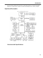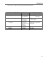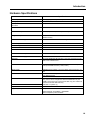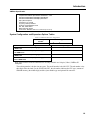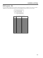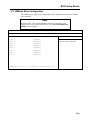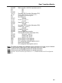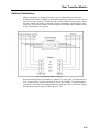
1
 XVME-689VR7
6U VME Intel® Celeron® M Processor Board
USER’S MANUAL
ACROMAG INCORPORATED
30765 South Wixom Road
P.O. BOX 437
Wixom, MI 48393-7037 U.S.A.
Tel: (248) 295-0885
Fax: (248) 624-9234
Email: [email protected]
Copyright 2012, Acromag, Inc., Printed in the USA.
Data and specifications are subject to change without notice.
8500-978D Revision
A
B
C
D
Description
Init
Errors in J2 and P0 pin-out
Error Correction
Error Correction
Date
02/08
09/09
02/10
12/10
Part Number 74689-VR7
Trademark Information
Brand or product names are trademarks or registered trademarks of their respective owners.
Intel and Pentium are registered trademarks and Celeron is a trademark of Intel Corporation.
Windows, Windows NT, Windows 2000 and Windows XP are registered trademarks of Microsoft
Corporation in the US and in other countries.
Copyright Information
This document is copyrighted by Xembedded, Incorporated (Xembedded) and shall not be
reproduced or copied without expressed written authorization from Xembedded.
The information contained within this document is subject to change without notice. Xembedded
does not guarantee the accuracy of the information.
WARNING
This is a Class A product. In a domestic environment this product may cause radio interference,
in which case the user may be required to take adequate measures.
Warning for European Users – Electromagnetic Compatibility
European Union Directive 89/336/EEC requires that this apparatus comply with relevant ITE
EMC standards. EMC compliance demands that this apparatus is installed within a VME
enclosure designed to contain electromagnetic radiation and which will provide protection for the
apparatus with regard to electromagnetic immunity. This enclosure must be fully shielded. An
example of such an enclosure is a Schroff 7U EMC-RFI VME System chassis, which includes a
front cover to complete the enclosure.
The connection of non-shielded equipment interface cables to this equipment will invalidate
European Free Trade Area (EFTA) EMC compliance and may result in electromagnetic
interference and/or susceptibility levels that are in violation of regulations which apply to the
legal operation of this device. It is the responsibility of the system integrator and/or user to apply
the following directions, as well as those in the user manual, which relate to installation and
configuration:
All interface cables should be shielded, both inside and outside of the VME enclosure.
Braid/foil type shields are recommended for serial, parallel, and SCSI interface cables.
Where as external mouse cables are not generally shielded, an internal mouse interface
cable must either be shielded or looped (1 turn) through a ferrite bead at the enclosure
point of exit (bulkhead connector). External cable connectors must be metal with metal
back-shells and provide 360-degree protection about the interface wires. The cable shield
must be terminated directly to the metal connector shell; shield ground drain wires alone
are not adequate. VME panel mount connectors that provide interface to external cables
ii
(e.g.,
RS232, USB, keyboard, mouse, etc.) must have metal housings and provide direct
connection to the metal VME chassis. Connector ground drain wires are not adequate.
Environmental Protection Statement
This product has been manufactured to satisfy environmental protection requirements where
possible. Many of the components used (structural parts, printed circuit boards, connectors,
batteries, etc.) are capable of being recycled.
Final disposition of this product after its service life must be accomplished in accordance with
applicable country, state, or local laws or regulations.
iii
Table of Contents
Table of Contents
XVME-689-VR7........................................................................................................................... i
Table of Contents ......................................................................................................................................v
Table of Figures and Tables ................................................................................................................... vii
Chapter 1 – Introduction ....................................................................................................... 1-1
Module Features ................................................................................................................................. 1-1
Architecture ........................................................................................................................................ 1-2
Software Support ................................................................................................................................ 1-5
Operational Description ...................................................................................................................... 1-6
Environmental Specifications ............................................................................................................. 1-6
Hardware Specifications ..................................................................................................................... 1-8
VMEbus Specification........................................................................................................................ 1-9
System Configuration and Expansion Options Tables ....................................................................... 1-9
Chapter 2 – Installation and Setup....................................................................................... 2-1
3Jumper Settings................................................................................................................................. 2-2
Switch Settings ................................................................................................................................... 2-3
Registers.............................................................................................................................................. 2-3
Front Panel Layout.............................................................................................................................. 2-5
Connectors .......................................................................................................................................... 2-6
COM1 and COM4 (J4) Pin Definitions............................................................................................... 2-10
purpose.VMEbus P2 Connector ......................................................................................................... 2-12
VMEbus P2 Connector........................................................................................................................ 2-13
Installing the XVME 689-VR7 into a Backplane ............................................................................. 2-18
Enabling the PCI Ethernet Controller ............................................................................................... 2-20
Chapter 3 BIOS Setup Menus............................................................................................... 3-1
3.1 Main Setup Menu.......................................................................................................................... 3-2
3.2 Exit Menu ..................................................................................................................................... 3-4
3.3 System Boot Menu........................................................................................................................ 3-5
3.4 POST Memory Tests..................................................................................................................... 3-9
3.5 Plug and Play Configuration Menu............................................................................................. 3-12
3.6 BIOS Super I/O Configuration Menu ......................................................................................... 3-15
3.7 BIOS Super I/O Configuration Menu ......................................................................................... 3-17
3.8 Firmbase® Technology Configuration ....................................................................................... 3-19
3.9 Misc. Menu ................................................................................................................................. 3-20
3.10 VMEbus Master ........................................................................................................................ 3-24
3.12 Front Panel resources control.................................................................................................... 3-28
Chapter 4 Programming........................................................................................................ 4-1
Memory Map ...................................................................................................................................... 4-1
I/O Map............................................................................................................................................... 4-1
IRQ Map ............................................................................................................................................. 4-3
v
Table of Contents
PCI Device Map – ................................................................................................................................. 4-4
VME Interface .................................................................................................................................... 4-5
Software-Selectable Byte-Swapping Hardware.................................................................................. 4-7
Appendix A SDRAM and Battery Installation ......................................................................... 1
Memory Type .........................................................................................................................................1
Installing SDRAM ..................................................................................................................................1
Module Battery Installation ....................................................................................................................2
Index ..........................................................................................................................................................4
vi
Table of Contents
Table of Figures and Tables
Figure 1-1 XVME 689-VR7 Block Diagram ............................................................................... 1-6
Figure 3-1 Main Setup Menu ....................................................................................................... 3-2
Figure 3-2 Slave Interface Submenu .......................................................................................... 3-26
Figure 4-1 Byte Ordering Schemes .............................................................................................. 4-8
Figure 4-2 Address-Invariant Translation .................................................................................... 4-8
Figure 4-3 Maintaining Numeric Consistency ............................................................................. 4-9
Figure 4-4 Maintaining Address Consistency ............................................................................ 4-10
Table 1-1 Maximum Video Modes Supported............................................................................. 1-3
Table 1-2 XVME 689-VR7 CPU configurations ......................................................................... 1-9
Table 1-3 XVME 689-VR7 Expansion Module Options ........................................................... 1-10
Table 2-1 XVME 689-VR7 Jumper Settings............................................................................ 2-2
Table 2-202 XVME 689-VR7 PMC Host Connector 2 Pin out ................................................. 2-17
Table 3-1 Slave Interface Submenu ........................................................................................... 3-27
vii
Introduction
Chapter 1 – Introduction
The XVME 689-VR7 VMEbus Intel® Celeron® M PC-compatible VMEbus processor module combines
the high performance and ruggedized packaging of the VMEbus with the broad application software base
of the IBM PC/AT standard. It integrates the latest processor and chipset technology. The XVME 689VR7is the lowest power draw of any of our processors while maintaining a very high level of processing
power.
NOTE:
The VR7 is a replacement board that is designed to
fit into the same chassis as a SBS built VR7.
Xembedded has no RTM for the rear I/O. If you
find you need an RTM please contact the factory.
Module Features
The XVME 689-VR7 offers the following features:
•
•
•
•
•
•
•
•
•
•
•
•
•
•
•
•
The XVME 689-VR7 is configured with the Intel Celeron M Celeron M Processor at 1.0GHZ.
Both processor models can be configured with 256MB to 2GB SDRAM.
1Mb on die level 2 cache on Celeron M 1.0GB (running at the speed of the processor).
Integrated Video controller using shared system DRAM for VRAM
Enhanced IDE controller, capable of driving two EIDE devices on P2 (NOT compatible with
the XVME-977 or XVME-979).
Two channels of SATA-150 out P2. Use the XVME 990-VR7 to provide the connectors needed
to connect external SATA drives.
Floppy disk controller, capable of driving one floppy drive on P2 (NOT Compatible with
XVME-977)
Dual 10/100/1000 Base T Ethernet controllers with front panel RJ-45 connectors with isolated
ground or selectable out the P0 to support rear Ethernet or Vita 31.1.
Type I/II Compact Flash site on optional carrier
VME64X VMEbus interface with programmable hardware byte swapping
Support for Vita 31.1 Switch Fabric in complaint back planes
Four serial ports:
• Two RS-232 serial port on front panel (Com 1 and 4) two RS-232 serial port (Com 2 and 3)
on P2. NOTE COM 4 is also available out the P2 and can be configured for RS232/422/485
Three Universal Serial Bus (USB 2.0) port one on front the other two out P2.
EPP/ECP configurable parallel port (P2) on 26-pin header on the XVME 990-VR7
Combined PS/2 compatible keyboard/mouse port on front panel
PCI 80-pin Expansion Connectors (NOT Compatible with XVME-976-01 thru XMVE-976-205
Carriers) must use the XVME-976-209.
PMC (PCI Mezzanine Card) site with front panel I/O 32/64-bit 33/66MHz with rear I/O using
optional P0 connector. This site is on the internal PCI-X bus.
1-1
Introduction
•
•
•
•
Front panel ABORT/RESET switch with indicating lights. Red for “fail” and green for “pass”
Electrical isolation and noise immunity on the Ethernet ports, Serial Port, and PMC site.
Ejector type handles in IEEE 1101.10 (Compact PCI type) or IEEE 1101.1 (legacy VME type).
VME64 VMEbus interface with programmable hardware byte swapping
Architecture
CPU Chip
The Intel Celeron M processors have a new micro-architecture, but remain software
compatible with previous members of the Intel microprocessor family. The Celeron M has
longer pipeline stages and thus does more per clock cycle, which allows it to run at a lower
clock frequency thus saving power. The Celeron M has a large L2 cache (1MB on 160nm)
which boosts performance. A Celeron M is comparable in performance to a Pentium 4
running at 50% higher clock rate, but dissipates less than half the power. With a junction
temperature range of 0 to 100C, and a max power dissipation ranging from 10W to 24Watts,
the Celeron M is capable of withstanding a great deal of thermal stress while reducing the
overall power dissipation for the product.
PCI Local Bus Interface
The Intel 855GME / 6300ESB chipset supports the Celeron M processors with up to 400MHz front
side bus. The XVME 689-VR7 incorporates one PCI-X bus which is used to service the two Intel
82546EB Ethernet controllers and the on-board PMC site. The PMC site supports both 32-bit/33MHz
and 64-bit/66MHz bus speeds with 5V I/O support. The XVME 689-VR7 supports on PCI bus for 32bit/33MHz operation, this bus services the PCI to VME bridge chip known as the tundra Universe II
chip and the 80-pin expansion connector used to connect the XVME-976-209 Dual PMC carrier
modules. These carrier modules can be “stacked” to allow for up to five (5) PMC sites on one XVME
689-VR7.
PCI-X, or PCI extended, is an enhanced version of PCI (Peripheral Component Interconnect)
computer bus. Although PCI-X is backward-compatible with traditional PCI devices and systems, this
specification implements additional features and performance improvements include 3.3V signaling,
increased speed grades, and adaptation to other form factors. PCI-X effectively doubles the speed and
amount of data exchanged between the computer processor and peripherals. PCI-X bus was designed
for and is ideally suited for server cards such as Fibre Channel, RAID, high-speed networking, and
other demanding devices.
Onboard Memory
SDRAM Memory
The XVME 689-VR7 has a socket for a single 200-pin SODIMM, providing 256 MB, 512MB, 1GB
and 2GB of ECC DDR 266/333MHz SDRAM. Approved SDRAM suppliers are listed in 0.
Flash BIOS
The XVME 689-VR7 system BIOS is contained in a 1MB flash device to facilitate system BIOS
updates. Contact Xembedded support for available updates at [email protected] if needed. Be
sure to record your current version number and the reason for the request.
1-2
Introduction
Video Controller
The 855GME Graphics and Memory Controller Hub (GMCH) has a built-in 2D/3D graphics controller. The
maximum video modes supported are listed in the following table. The highest supported interlaced monitor
mode is 1280x1024, 16-bit/65k color, and 43 Hz. Video output is available on the front panel through a
standard 15-pin D shell connector. The graphics controller is in the 855GME which uses up to 64MB main
memory as video memory. The 855GME has a built-in 3D graphics engine and its display / render core
frequency is up to 200MHz.
Table 1-1 Maximum Video Modes Supported
Resolution
640x480
800x600
1024x768
1280x1024
1600x1200
Bit Depth/Colors
24-bit/16M color
24-bit/16M color
24-bit/16M color
24-bit/16M color
16-bit/65k color
Vertical Refresh
100 Hz
100 Hz
100 Hz
75 Hz
60 Hz
Ethernet Controller
The 82546GB dual Giga-bit Ethernet controller provides a pair of 10/100/1000baseT Ethernet interfaces. The
82546GB contains both the MAC and the physical layer. The RJ-45 connectors on the module's front panel
provide auto-sensing for 10Base-T, 100Base and 1000Base -TX connections. Each RJ-45 connector has two
indicator lights. When mounted vertically, the top light is the link/activity light and the bottom light (the one
closer to the COM ports) is the 10Base-T/100Base-TX indicator. When it is off, the connection is 10Base-T;
when it is on, the connection is 100Base-TX. When the Ethernet is switched to the rear optional P0 no lights
are available to indicate link or speed. Storage Devices (Hard Drive, Floppy, Compact PCI and On-Board
Drive)
EIDE and Floppy Drives
The XVME 689-VR7 primary IDE and floppy drive signals are routed through the P2 connector inner three
rows (available in a legacy 96-pin back plane), providing a simplified method of connecting up to two IDE
devices and one external floppy drive. The secondary IDE master signals support the optional on-board hard
drive or on-board Compact Flash site and the secondary IDE slave signals are not supported.
The XVME-689-VR7 is NOT compatible with the XVME-977 and/or the XVME-979 mass storage modules.
1-3
Introduction
Caution
The IDE controller supports enhanced PIO modes, which reduce the cycle times for
16-bit data transfers to the hard drive. Check with your drive manual to see if the
drive you are using supports these modes. The higher the PIO mode, the shorter the
cycle time. As the IDE cable length increases, this reduced cycle time can lead to
erratic operation. As a result, it is in your best interest to keep the IDE cable as
short as possible.
The PIO modes can be selected in the BIOS setup. The Auto configuration will
attempt to classify the connected drive if the drive supports the auto ID command.
If you experience problems, change the Transfer Mode to Standard.
Caution
The total cable length must not exceed 18 inches. Also, if two drives are connected,
they must be no more than six inches apart. See SATA below for longer cable
lengths.
Serial ATA Hard Drive
The XVME 689-VR7 features two (2) SATA-150 drive interfaces out the rear P2 VMEbus connector. The
use of the optional rear transition module (XVME 990-VR7) allows for the connection of two drives using
standard SATA cables. If your application requires the external drives to be mounted in a location that
requires a long cable run, the SATA drives are better suited to that application. SATA cable can be up to 1
meters or 39” long, EIDE have be less than 18” long.
On-Board Hard Drive (Optional module XVME-913)
The on-board hard drive resides as a master on the secondary EIDE port. The XVME-913 is a kit of parts
including; 1.8” hard drive, cable, 4 brackets, screws and standoffs. There are no unique drivers required.
The XVME 689-VR7 can be booted from the on-board hard drive if configured in the BIOS Boot menu.
NOTE: The XVME 689-VR7 module can accept either an on-board 1.8” hard drive (XVME-913) or the
Compact Flash carrier (XVME-912) but not both.
Compact Flash Site (Optional module XVME-912)
The compact flash socket on the optional carrier module will support type I or type II Compact Flash cards.
The compact flash resides as a master on the secondary IDE port. There are no unique drivers required. The
XVME 689-VR7 can be booted from the compact flash drive if configured in the BIOS Boot menu. NOTE:
The XVME 689-VR7 module can accept either an on-board 1.8” hard drive (XVME-913) or the Compact
Flash carrier (XVME-912) but not both.
VMEbus Interface
The XVME 689-VR7 uses the PCI local bus to interface to the VMEbus via a PCI to VME bridge device (Tundra
Universe IID). The VMEbus interface supports full DMA to and from the VMEbus, integral FIFOs for posted writes,
block mode transfers, and read-modify-write operations. The interface contains one master and eight slave images
that can be programmed in a variety of modes to allow the VMEbus to be mapped into the XVME 689-VR7 local
memory. This makes it easy to configure VMEbus resources in protected and real mode programs The XVME 689VR7 also incorporates onboard hardware byte-swapping (see Table 1-2). For a complete API, the Xembedded Board
Support Packages tailored to your operating system will allow quick programming of your application.
1-4
Introduction
Serial and Parallel Ports
XVME-689-VR7 includes four high-speed 16550-compatible serial ports (RS-232C) with Com 4 capable of RS-232
and RS-422/485 configurations. The Parallel port can be configured for ECP or EPP parallel port. This is done in the
SMC SCH3114 LPC Super I/O and programmed via the BIOS. Com ports 1 and 4 are RJ-45’s on the front panel and
Com 2 and 3 are available out the P2 VMEbus. The COM 4 port differ from front to back (P2), the front COM port 4
CAN NOT be configured as a RS-232/422/485 but the rear P2 COM port 4 can be configured in this way.
Keyboard / Mouse Interface
A combined keyboard and mouse port PS/2 connector is provided on the front panel. A PS/2 splitter cable part
number 140232 (provided with the module) may be used to separate the two ports so that both devices may be
simultaneously connected to the module. IF a mouse is not required, a keyboard can be connected directly to the
PS/2 port. The keyboard and mouse are controlled in the SMC SCH3114 LPC Super I/O.
PMC Expansion
The XVME 689-VR7 provides an on-board PMC site for use with standard 32/64-bit, 33/66MHz PMC and PMC-X
modules. The PMC site is serviced by the on-board PCI-X bus. For electrical isolation, the PMC front panel bezel is
not connected to the main CPU ground. PCI-X, or PCI extended, is an enhanced version of PCI (Peripheral
Component Interconnect) computer bus. Although PCI-X is backward-compatible with traditional PCI devices and
systems, this specification implements additional features and performance improvements include 3.3V signaling,
increased speed grades, and adaptation to other form factors. PCI-X effectively doubles the speed and amount of data
exchanged between the computer processor and peripherals. PCI-X bus was designed for and is ideally suited for
server cards such as FPGA, DSP, Fibre Channel, RAID, high-speed networking, and other demanding devices. If a
standard PCI PMC card is fitted on the XVME 689-VR7 PMC site, the on-board PCI-X bus reverts to the PCI bus
speed.
Additional PMC Expansion Options
The XVME 689-VR7 supports optional PMC (PCI Mezzanine Card) expansion using XVME-976-209 expansion
module. The XVME-976-209 provides two PCI Mezzanine Card (PMC) sites. The XVME-976-209 module is
designed to plug directly into the XVME 689-VR7 using the 80-pin expansion board connector. Another XVME976-209 can be used to extend the XVME 689-VR7 and first XVME-976-209 to five PMC card sites.
Watchdog Timer
The XVME 689-VR7 has a long duration watchdog timer which can count from 1 to 255 seconds or from 1 to 255
minutes. The BIOS supports various system events which can be routed to the watchdog timer. The timer when
enabled can generate either an interrupt or a master reset depending on how the watchdog timer is configured.
Note
The timeout range is from 1.0 second to 2.25 seconds; it will typically be 1.6
seconds.
Software Support
The XVME 689-VR7 is fully PC-compatible and will run "off-the-shelf" PC software, but most packages
will not be able to access the features of the VMEbus. To solve this problem, Xembedded has developed
extensive Board Support Packages (BSPs) that simplify the integration of VMEbus data into PC software
applications. Xembedded’s BSPs provide users with an efficient high-level interface between their
1-5
Introduction
applications and the VMEbus-to-PCI bridge device. Board Support Packages are available for MS-DOS®,
Windows NT®, Windows 2000®, Windows XP, Windows XP Embedded, Linux, VxWorks, and QNX®.
Operational Description
Figure 1-1 XVME 689-VR7 Block Diagram
Environmental Specifications
1-6
Introduction
The XVME 689-VR7 will meet the following environmental requirements:
Environmental Specification
Operating
Non-Operating
-40 to 85 C
Thermal
Humidity
10% to 90% RH,
non-condensing
10% to 90% RH, noncondensing
Shock
30 g peak
acceleration, 11
msec duration
50 g peak acceleration,
11 msec duration
Vibration
5 – 2000 Hz
0.015” (0.38mm)
peak-to-peak
displacement, 2.5 g
maximum
acceleration
0.030” (0.76mm) peak-to-peak
displacement, 5 g maximum
acceleration
Emissions
EN 55022
EN 55022
Immunity
EN 50082-2
EN 50082-2
1-7
Introduction
Hardware Specifications
Characteristic
Specification
Power Specifications:
5.4 A (typical); 10.5 A (maximum)
Voltage Specifications:
+5V, +12V, -12V; all +5%/-2.5%
CPU speed: Intel Celeron M Low Power
Processor
1.8 GHz
L2 Cache: Intel Celeron M Low Power Processor
2 MB
Onboard memory
SDRAM, up to 2 GB (one 200-pin SODIMM)
Integrated Graphics Controller
1600 x 1200 maximum resolution, 24-bit color maximum; 4 MB
Shared memory
Ethernet Controllers (2)
Intel 82546GB 10/100/1000Base-TX Gigabit Ethernet; RJ-45
Mass Storage
Integrated SATA-150 Controller
EIDE Ultra DMA 100 interface
Compact Flash
Floppy Drive
PMC Site
SATA0 and SATA1 via P2
2 channels via P2
One 1.8" on-board EIDE via optional carrier module
One, on-board Compact flash site via optional carrier module
Via P2 to XVME 977
On board 66 MHz/64 Bit PMC/PCI-X with front and P0 I/O Access.
Site is 3.3V interface level
Optional 32bit / 33 MHz sites available via XVME-976-209 (2 sites,
total 3) and XVME-976-210 (4 sites, total 5)
Stereo Audio
AD1981B AC97 CODEC, Line Level Stereo Input and Output Via
P2
USB
One USB 2.0 via Front panel
Two USB 2.0 via P2
Serial Ports
Parallel Interface
RS-232C, 16550 compatible (4) COM1 Front, Com 2 and 3 Rear
I/O, (Com 4 can be configured for RS-232/422/485 but only the
COM 4 out the P2, Com 2 and 3 are RS-232 only). The COM 4 out
the front is RS-232 data leads only.
EPP/ECP compatible (1)
Keyboard and Mouse
Via Front Panel
Regulatory Compliance
European Union – CE;
Electromagnetic Compatibility - 89/336/EEC
RoHS Compliant product available
1-8
Introduction
VMEbus Specification
VMEbus Compliance
Complies with VMEbus Specification ANSI/VITA 1–1994
A32/A24/A16:D64/D32/D16/D08(EO) DTB Master
A32/A24/A16:D64/D32/D16/D08(EO) DTB Slave
R(0-3) Bus Requester
Interrupter I(1)-I(7) DYN
IH(1)-IH(7) Interrupt Handler
SYSCLK and SYSRESET Driver
PRI, SGL, RRS Arbiter
RWD, ROR bus release
Form Factor: DOUBLE 233.7 mm x 160 mm (9.2" x 6.3")
System Configuration and Expansion Options Tables
Table 1-2 XVME 689-VR7 CPU configurations
Ordering
CPU Type
Number
®
®
XVME 689-VR7/1XY
Intel Celeron M 1.0GHz
Handle and P0 configurations
Memory configurations
Y = 1 VME-64 IEEE 1101.1 (Std / legacy) handles w/o
X = 1 for 256 MB ECC DRR SDRAM
VMEbus P0
Y = 2 VME-64 IEEE 1101.10 (Compact PCI type) handles
X = 2 for 512 MB ECC DRR SDRAM
w/o VMEbus P0
Y = 3 VME-64 IEEE 1101.1 (Std / legacy) handles with the X = 3 for 1 GB ECC DRR SDRAM
VMEbus P0
Y = 4 VME-64 IEEE 1101.10 (Compact PCI type) handles
with the VMEbus P0
Note: Some features on the XVME 689-VR7 are only available in a 160-pin (5-Row) VMEbus P2
backplane.
The ordering number is broken into two parts. The model number is the 689-VR7. The tab number is the
three digits after the slash. For the XVME 689-VR7, the tab number indicates the CPU type, amount of
SDRAM memory (the middle digit) and the ejector handle type and optional P0 connector.
1-9
Introduction
.
Table 1-3 XVME 689-VR7 Expansion Module Options
Ordering Number
XVME 990-VR7/1
XVME 990-VR7/2
XVME-976-209
XVME-977/011
XVME-979/1
XVME-979/2
XVME-979/3
XVME-979/4
XVME-979/5
XVME-979/6
XVME-9000-EXF
Description
Drive Adapter Module for external drives, cables out back of VME
backplane, Primary PIDE (2 PIDE), Floppy, COM2 (Only RS-232),
two ports of SATA-150, LPT1, 1 USB port, Audio in/out and
Analog Video out plus P0 for rear I/O from PMC site and Ethernet
31.1 or rear RJ-45 Ethernet.
Drive Adapter Module for external drives, cables out back of VME
backplane, Primary PIDE (2 PIDE), Floppy, COM2 (Only RS-232),
two ports of SATA-150, LPT1, 1 USB port, Audio in/out and
Analog Video out
PMC Carrier module with two PMC module sites. The XVME-976209 allows for stacking of a second XVME-976-209, this
combination will accommodate a total of five PMC modules
Not Compatible with the XVME-689-VR7
Not Compatible with the XVME-689-VR7
Not Compatible with the XVME-689-VR7
Not Compatible with the XVME-689-VR7
Not Compatible with the XVME-689-VR7
Not Compatible with the XVME-689-VR7
Not Compatible with the XVME-689-VR7
Not Compatible with the XVME-689-VR7
The XVME 990-VR7 is described in Error! Reference source not found..
1-10
Installation and Setup
Chapter 2 – Installation and Setup
Board Layout
This chapter provides information on configuring the XVME 689-VR7 modules. It also provides information on
installing the XVME 689-VR7 into a backplane and enabling the Ethernet controller.
Fig. 2-1 shows the jumper, switch, and connector locations on the XVME 689-VR7.
2-1
Installation and Setup
3
Jumper Settings
The following table Lists XVME689-VR7 jumpers, their default positions, and their functions.
Table 2-1 XVME 689-VR7 Jumper Settings
Jumper
JP2
JP3
2
JP4
JP5
JP6
JP7
JP8
JP60
JP61
JP62
Position
A
B √
A
B √
A √
B
A √
B
A √
B
A
B √
A √
B
Function
XVME 689-VR7 cannot generate SYSFAIL*
XVME 689-VR7 generates SYSFAIL* normally
Disables system resources (no auto SYSCON)
Enables system resources (auto SYSCON)
XVME 689-VR7 can reset VMEbus
XVME 689-VR7 cannot reset VMEbus
Normal
Clear CMOS
Boot from FLASH
Boot from ROM
Orb ground not connected to logic ground
Orb ground connected to logic ground
1 ----- 2
3
4
5
6
1 ----- 2
2
3
4 ----- 5
5
6
7 ----- 8
8
9
10 ----11
11
12
Normal (Video out Front Panel VGA)
Video re-routed to P2 connector (no video out front
panel)
SIO_COM_RXD 4 = RXD4
SIO_COM_RXD 4 = RXD422
SIO_COM_RXD 4 = RXD485
DCD4
485TXDDSR4
485TXD+
RI4
485RXDDTR4
485RXD+
A√
B
RS-232
RS-422/RS-485
denotes default
2-2
Installation and Setup
Switch Settings
The XVME 689-VR7 has one four-pole switch (SW1) shown in Figure 2-2. The switches
functions are explained in table 2-2. This switch controls the system response to the front panel
Abort switch. Figure 2-2 shows the switch settings required to reset on the XVME 689-VR7
CPU, to reset only the VME backplane, or to reset both. The XVME 689-VR7 is shipped with
all four switches in the closed position (which causes the push button reset switch to reset both
the XVME 689-VR7 and the VME backplane).
Figure. 2-2
SW1 XVME 689-VR7 has a 4 position DIP switch to control the following functions.
Table 2-2 Four-Pole Switch (SW1) Functions
Position
1
2
3
4
Open
Do not respond to SYSRESET*
Toggle switch does not cause SYSRESET*
SYSFAIL* asserted on Power Up
No local reset
Closed
Respond to SYSRESET*
Toggle switch causes SYSRESET*
SYSFAIL* not asserted on Power
Toggle switch causes local reset
Registers
The XVME 689-VR7 modules contain the following Xembedded-defined I/O registers: 218h,
219h, 233h, and 234h.
Register 218h – Abort/CMOS Clear Register
This register controls the abort toggle switch and allows you to read the CMOS clear jumper
(main board J21).
Table 2-3 Abort/CMOS Clear Register Settings
Bit
0
1
2
3
4
5
Signal
RESERVED
RESERVED
RESERVED
RESERVED
ABORT_STS
ABORT_CLR
6
7
RESERVED
CLRCMOS
Result
Reserved
Reserved
Reserved
Reserved
1 = Abort toggle switch caused interrupt
0 = Clear and disable abort
1 = Enable abort
Reserved
0 = Clear CMOS
1 = CMOS okay
R/W
R
R/W
R
2-3
Installation and Setup
Register 219h – Flash Control Register
This register controls the following LEDs and signals.
Table 2-4 LED/BIOS Register Settings
Bit
1
0
LED/Signal
FAULT
1
PASS
2
1
3
1
4
1
5
1
6
1
7
Result
N/A
0 = Fault LED on
1 = Fault LED off
0 = PASS LED off
1 = PASS LED on
N/A
N/A
RESERVED
RESERVED
RESERVED
RESERVED
N/A
Reserved
Reserved
Reserved
Reserved
R/W
R/W
R/W
Register 233h – Watchdog Timer Register
This register controls watchdog timer operation.
Table 2-5 Watchdog Timer Register Settings
Bit
0
1
2
3
4
5
Signal
RESERVED
RESERVED
RESERVED
RESERVED
WDOG_EN
MRESET_EN
6
7
WDOG_STS
WDOG_CLR
Result
Reserved
Reserved
Reserved
Reserved
1 = Enables the watchdog timer
1 = Timeout generates
0 = Timeout generates IRQ10
Watchdog timer status bit
Toggling this bit clears the watchdog timer
back to a zero count.
Note
Before enabling the watchdog timer for the first time, it is necessary to reset the
count back to zero by toggling bit 7 (WDOG_CLR). Toggling implies changing
the state of bit (0 to 1 or 1 to 0).
2-4
Installation and Setup
Register 234h – Flash Paging and Byte Swap Register
This register controls access to the Flash paging and byte-swapping functions.
Table 2-6 Flash Paging and Byte Swap Register Settings
Bit
0
1
2
3
4
5
6
7
Signal
FLB_A15
FLB_A16
FLB_A17
Unused – set to 0
Unused – set to 0
Unused – set to 0
SWAPS
SWAPM
Result
Flash address 15 - page control bit
Flash address 16 - page control bit
Flash address 17 - page control bit
Do not use.
Do not use.
Do not use.
1 = No swapping (data invariant) occurs during slave cycles
1 = No swapping (data invariant) occurs during master cycles
Front Panel Layout
Panel LEDs and Switch
The reset switch can be enabled to reset see the setup of Sw-1 shown in Figure 2-2 and table 2-2. This switch can
be configured to either just reset the XVME 689-VR7 or to reset both the VMEbus and the XVME 689-VR7.
The green pass and red fail LEDs are used as an indication of board health during the BIOS boot up. Both the
green pass and red fail LEDs will light during the POST of the board. As the BIOS complete the POST, the red
fail LED will be turned off. This is an indication the XVME 689-VR7 has passed the POST. The Green SYS
Controller LED is lit when the XVME 689-VR7 is configured as the VMEbus system controller. This is the
function that grants bus ownership to multiple bus VME masters and provides the 16MHz clock signal on the
back plane.
2-5
Installation and Setup
Connectors
This section provides pin outs for the XVME 689-VR7 connectors. Refer to the EMC warning at
the beginning of this manual before attaching cables.
Keyboard/Mouse Port Connector (P7)
Figure 2-7
Table 2-7 Keyboard Port Connector Pin out
Pin
1
2
3
4
5
6
Signal
Keyboard Data
Mouse Data
GND
+5V
Keyboard Clock
Mouse Clock
2-6
Installation and Setup
Front panel (P12 or Rear Ethernet Port and Vita 31.1 Ethernet
____________________________________________________________
The Ethernet ports on the XVME 689-VR7 are switch able between the front and the rear of the XVME 689VR7. When in the rear mode, the Ethernet port can use the PO connector for either Vita 31.1 switch fabric over
the Vita 31.1 compliant backplane or Ethernet out the rear or the module.
Table 2-8 RJ-45 10/100/1000 BaseT Connector Pin out
Figure 2-8 RJ-45 10/100/1000Mbps
Pin
1
2
3
4
5
6
7
8
Signal
TX+
TXRX+
GND
GND
RXGND
GND
2-7
Installation and Setup
VGA Connector (P9)
The video is BIOS selectable and is available on either the front panel on a standard SVGA connector or out the
VMEbus P2. The table below shows the pin out of the VMEbus P2 pin out for the rear access of video.
Figure 2-9 SVGA Connector
Table 2-9 VGA Connector Pin out
SVGA
Pin out
1
2
3
4
5
6
7
8
9
10
11
12
13
14
15
Signal
RED
GREEN
BLUE
NC
GND
GND
GND
GND
25MIL_VIDA
GND
NC
LDDCDAT
HSYNC
VSYNC
LDDCCLK
VMEbus P2
Row d Pin-20
Row d Pin-21
Row d Pin-22
N/C
Row d Pin-31
Row d Pin-31
Row d Pin-31
Row d Pin-31
N/C
Row d Pin-31
N/C
Row d Pin-26
Row d Pin-23
Row d Pin-24
Row d Pin-25
2-8
Installation and Setup
USB Port Connector (J5)
USB provides an expandable, hot-pluggable Plug and Play serial interface that ensures a
standard, low-cost connection for peripheral devices. Devices suitable for USB range from
simple input devices such as keyboards, mice, and joysticks, to advanced devices such as
printers, scanners, storage devices, modems, and video conferencing cameras. USB 2.0 has a
raw data rate at 480Mbps, and it is rated 40 times faster than its predecessor interface, USB 1.1,
which tops at 12Mbps.
USB port 1 is available on the front panel using a standard connector as shown in Figure 2-10
below. The other two USB ports USB-2 and 3, are routed out the VMEbus P2 connector and can
be accesses either directly off the VMEbus P2 connector using the pin assignment shown in Fig.
2-10. The USB +5 V supplies are protected with a polyswitch. This device will open up if +5 V
is shorted to GND. Once the shorting condition is removed, the polyswitch will allow current
flow to resume.
Figure 2-10 USB Connector
VMEbus P2
Signal Name
P2-row-z 17
USB3_GND
P2-row-z 18
GND
P2-row-z 19
USB3+
P2-row-z 20
GND
P2-row-z 21
USB3P2-row-z 22
GND
P2-row-z 23
USB3_PWR
P2-row-z 24
GND
P2-row-z 25
USB2_GND
P2-row-z 26
GND
P2-row-z 27
USB2+
P2-row-z 28
GND
P2-row-z 29
USB2P2-row-z 30
GND
P2-row-z 31
USB2_PWR
P2-row-z 32
GND
Table 2-11 Rear USB ports 2 and 3
USB Port Connector Pin out on VMEbus P2
Pin
Signal
1
+5V
2
USBP0-
3
USBP0+
4
GND
Table 2-10 USB Port Connector Pin out
2-9
Installation and Setup
COM1 and COM4 (J4) Pin Definitions
The XVME 689-VR7 has two serial ports out the front panel, Com 1 and Com 4, these two com ports use the RJ45 connector. Two more com ports are out the VMEbus P2 connector. See below for connector layout and pin
descriptions.
Figure 2-11 RJ-45 Serial Port Connectors
Com ports 1 and 4 Pin Definitions for front connectors
Pin Number
1
2
3
4
5
6
7
8
RS232
RTS
DTR
TXD
GND
GND
RXD
DSR
CTS
Table 2-13 Serial Port Connector Pin out for Comm-1 and 4
2-10
Installation and Setup
On-Board Hard Drive/Compact Flash Site (J17)
A horizontal ZIF connector is used on the board. (Samtec part number ZF5-40-01-TM-WT.) The
connector on the board has a reverse pin out because of the connector orientation relative to the hard
drive. This allows the flex cable to loop up to the hard drive, with the connector side facing the board.
Table 2-14 On-Board storage devices us the J17 1.8inch Hard Drive Connector pin assignment
Pin #
1
2
3
4
5
6
7
8
9
10
Description
factory use
factory use
RESETGROUND
DD7
DD8
DD6
DD9
DD5
DD10
Pin #
11
12
13
14
15
16
17
18
19
20
Description
DD4
DD11
DD3
DD12
DD2
DD13
DD1
DD14
DD0
DD15
Pin #
21
22
23
24
25
26
27
28
29
30
Description
GROUND
DMARQ
GROUND
DIOWDIORGROUND
IORDY
GROUND
DMACKINTRQ
Pin #
31
32
33
34
35
36
37
38
39
40
Description
DA1
PDIAGDA0
DA2
CS0CS1DASP3.3V
3.3V
DEVADR
The Hitachi C4K60 CE has a 40 pin ZIF connector.
Table 2-15 1.8inch Hard Drive Connector pin assignment on hard drive
Pin #
40
39
38
37
36
35
34
33
32
31
Description
factory use
factory use
RESETGROUND
DD7
DD8
DD6
DD9
DD5
DD10
Pin #
30
29
28
27
26
25
24
23
22
21
Description
DD4
DD11
DD3
DD12
DD2
DD13
DD1
DD14
DD0
DD15
Pin #
20
19
18
17
16
15
14
13
12
11
Description
GROUND
DMARQ
GROUND
DIOWDIORGROUND
IORDY
GROUND
DMACKINTRQ
Pin #
10
9
8
7
6
5
4
3
2
1
Description
DA1
PDIAGDA0
DA2
CS0CS1DASP3.3V
3.3V
DEVADR
2-11
Installation and Setup
VMEbus Connectors
VMEbus P1 Connector
Table 2-16 P1 Connector Pin out
Pin
1*
2
3*
4
5*
6
7*
8
9*
10
11*
12
13
14
15
16
17
18
19
20
21
22
23
24
25
26
27
28
29
30
31
32
Z
MPR
GND
MCLK
GND
MSD
GND
MMD
GND
MCTL
GND
RESP*
GND
SDB14*
GND
SDB15*
GND
SDBP1
GND
RSVBUS5
GND
RSVBUS6
GND
RSVBUS7
GND
RSVBUS8
GND
RSVBUS9
GND
RSVBUS10
GND
RSVBUS11
GND
A
D00
D01
D02
D03
D04
D05
D06
D07
GND
SYSCLK
GND
DS1*
DS0*
WRITE*
GND
DTACK*
GND
AS*
GND
IACK*
IACKIN*
IACKOUT*
AM4
A07
A06
A05
A04
A03
A02
A01
-12V
+5V
B
BBSY*
BCLR*
ACFAIL*
BG0IN*
BG0OUT*
BG1IN*
BG1OUT*
BG2IN*
BG2OUT*
BG3IN*
BG3OUT*
BR0*
BR1*
BR2*
BR3*
AM0
AM1
AM2
AM3
GND
NC
NC
GND
IRQ7*
IRQ6*
IRQ5*
IRQ4*
IRQ3*
IRQ2*
IRQ1*
NC
+5V
C
D08
D09
D10
D11
D12
D13
D14
D15
GND
SYSFAIL*
BERR*
SYSRESET*
LWORD*
AM5
A23
A22
A21
A20
A19
A18
A17
A16
A15
A14
A13
A12
A11
A10
A09
A08
+12V
+5V
D
+5V
GND
+V1
+V2
RSVU1
-V1
-V2
RSVU2
GAP*
GA0*
GA1*
GA2*
GA3*
GA4*
RSVBU1
RSVBU2
RSVBU3
RSVBU4
LI/I*
LI/O*
GND
+5V
Some pins in columns Z and D are use internally as test points, these are denoted by italics. These pins are not
intended to drive any external devices and MUST not be used for any purpose.
2-12
Installation and Setup
VMEbus P2 Connector
Pin
Number
1
2
3
Row Z
Row A
Row B
Row C
Row D
FD_DRV0
GND
FD_DIR
VGA_RED
VGA_GREEN
VGA_BLUE
USB0USB0+
USB1-
FD_INDX
FD_DCHG
FD_MTR0
4
5
6
7
8
GND
FD_WGAT
GND
FD_RDAT
GND
VGA_HSYN
GND
AUD_LINE_IN_L
AUD_LINE_IN_R
AUD_LINE_OUT_L
+5V
GND
VME_RETRY
*
A24
A25
A26
A27
A28
USB1+
VGA_VSYN
NC
NC
NC
FD_STEP
FD_WDAT
FD_TRK0
FD_WPRT
FD_HDSL
9
10
11
12
13
14
15
16
17
18
19
20
21
22
LPT1_AFED
GND
LPT1_ERRO
GND
LPT1_INT
GND
LPT1_SLIN
GND
LPT1_ACK
GND
LPT1_SLCT
GND
COM3_DSR
GND
AUD_LINE_OUT_R
GND
SATA_TXP0
SATA_TXN0
GND
SATA_RXP0
SATA_RXN0
GND
AUD_LINE_OUT_L
KYBD DATA
MOUSE DATA
ETH2 PIN 1(TXA+)
ETH2 PIN 3(RXA+)
ETH2 PIN 5(NC)
A29
A30
A31
GND
+5V
VD16
VD17
VD18
VD19
VD20
VD21
VD22
VD23
GND
LPT1_STRO
LPT1_D0
LPT1_D1
LPT1_D2
LPT1_D3
LPT1_D4
LPT1_D5
LPT1_D6
LPT1_D7
LPT1_BUSY
LPT1_PE
WDG_REL
COM3_DCD
COM3_RXD
23
24
25
26
COM3_TXD
GND
COM3_RI
GND
ETH2 PIN 7(NC)
COM1_DSR
COM1_RTS
COM1_CTS
VD24
VD25
VD26
VD27
NC
GND
SATA_TXP1
SATA_TXN1
GND
SATA_RXP1
SATA_RXN1
GND
\RST_BUT
KYBD CLK
MOUSE CLK
ETH2 PIN 2(TXA-)
ETH2 PIN 4(NC)
ETH2 PIN 6(RXA)
ETH2 PIN 8(NC)
COM1_DCD
COM1_RXD
COM1_TXD
27
COM4_RXD
COM1_RI
VD28
COM1_DTR
28
29
GND
COM4_CTS
COM2_DCD
VD29
VD30
GND
COM2_DSR
30
GND
31
COM4_RI(C
4_RXD-)
GND
32
COM3_RTS
COM3_CTS
COM3_DTR
COM4_DCD(C4_TXD
-)
COM4_DSR(C4_TXD
+)
COM4_RTS
COM2_RXD
COM2_TXD
VD31
COM2_RTS
COM2_DTR
GND
COM2_CTS
COM4_TXD
COM4_DTR(C4_RXD
+)
GND
GND
+5V
COM2_RI
+5V
Table 2-17 VMEbus P2 Connector
2-13
Installation and Setup
VMEbus P0 Connector
PIN
F
E
D
C
B
A
1
2
3
4
5
6
7
8
9
10
11
12
13
14
15
16
17
18
19
GND
GND
GND
GND
GND
GND
GND
GND
GND
GND
GND
GND
GND
GND
GND
GND
GND
GND
GND
IDE_PDDACK#
IDE_PDDREQ
GND
IDE_PDDCS1#
IDE_PDDA0
IDE_PDDA1
IDE_IRQ14
IDE_PIORDY
IDE_PIORDR#
IDE_PIORDW#
IDE_PDD0
IDE_PDD1
IDE_PDD2
IDE_PDD3
IDE_PDD4
IDE_PDD5
IDE_PDD6
IDE_PDD7
IDE_PDRST#
N/C
N/C
N/C
N/C
N/C
N/C
N/C
N/C
IDE_PDCS3
IDE_PDA2
IOCS16#
IDE_PDD15
IDE_PDD14
IDE_PDD13
IDE_PDD12
IDE_PDD11
IDE_PDD10
IDE_PDD9
IDE_PDD8
N/C
N/C
N/C
N/C
N/C
N/C
N/C
N/C
N/C
N/C
N/C
N/C
N/C
N/C
N/C
N/C
N/C
N/C
N/C
N/C
PMC I/O 17
PMC I/O 18
PMC I/O 19
PMC I/O 33
PMC I/O 20
PMC I/O 34
PMC I/O 21
PMC I/O 22
PMC I/O 23
PMC I/O 24
PMC I/O 25
PMC I/O 26
PMC I/O 32
PMC I/O 1
PMC I/O 2
PMC I/O 3
PMC I/O 4
PMC I/O 5
PMC I/O 6
PMC I/O 7
PMC I/O 8
PMC I/O 35
PMC I/O 9
PMC I/O 10
PMC I/O 11
PMC I/O 12
PMC I/O 13
PMC I/O 14
GND
PMC I/O 27
PMC I/O 28
PMC I/O 29
PMC I/O 30
PMC I/O 31
GND
PMC I/O 15
PMC I/O 16
2-14
Installation and Setup
80pin PCI connector (P3)
The P3, high speed micro-strip connector has all the PCI signals along with 2 separate PCI clocks and the 2 request and
grants predefined. The CPU board and the Interface boards will be keyed for either 3.3V or 5V signaling. The keying
mechanism is based on standoffs. At this point all CPU boards will be 5V PCI signaling. The V/IO pins on the connector are
used to define the signaling level to the other PCI boards. This connector is used to attach the XVME-976-209 dual PMC
carrier. The XVME-976-209 can support one additional carrier module stacked to create a three slot set of boards that can
support five PMC cards.
Table 2-18 PCI bus interconnect for optional carrier module
P3 Pin Number
1
2
3
4
5
6
7
8
9
10
11
12
13
14
15
16
17
18
19
20
21
22
23
24
25
26
27
28
29
30
31
32
33
34
35
36
37
38
39
40
Name
TCLK (P.D.)
TRST* (P.D.)
TMS (P.U.)
TDO (NC)
TDI (P.U.)
+12v
+12V
NC
NC
-12V
-12V
NC
NC
NC
NC (PCLKS3) (note 1)
PIRQA*
PIRQB*
PIRQC*
PIRQD*
REQ3*
NC(PCLKS2) (note 1)
REQ1*
GNT3*
PCICLK1
GNT1*
PCIRST*
PCICLK0
GNT0*
REQ0*
REQ2*
AD(31)
AD(30)
AD(29)
AD(28)
AD(27)
AD(26)
AD(25)
AD(24)
BE3*
GNT2*
P3 Pin Number
41
42
43
44
45
46
47
48
49
50
51
52
53
54
55
56
57
58
59
60
61
62
63
64
65
66
67
68
69
70
71
72
73
74
75
76
77
78
79
80
Name
AD(23)
AD(22)
AD(21)
AD(20)
AD(19)
AD(18)
AD(17)
AD(16)
BE2*
FRAME*
IRDY*
TRDY*
DEVSEL*
STOP*
PLOCK*
PERR*
SDONE (P.U.)
SBO*
(P.U.)
SERR*
PAR
BE1*
AD(15)
AD(14)
AD(13)
AD(12)
AD(11)
AD(10)
AD(9)
AD(8)
BE0*
AD(7)
AD(6)
AD(5)
AD(4)
AD(3)
AD(2)
AD(1)
AD(0)
ACK64* (P.U.)
REQ64* (P.U.)
Although not shown, the P3 connector supplies Vi/o = +5v, VCC=+5V, and GND through the center pins. Notes: (1)
PCICLK2 and PCICLK3 are not supplied by the XVME 689-VR7. These clocks were needed for on board PCI devices and
were not used by any currently supported daughtercards.
2-15
Installation and Setup
PMC Host Connectors
PMC Host Connector 1
Table 2-19 XVME 689-VR7 Daughterboard PMC Host Connector 1 Pin out
Pin
1
2
3
4
5
6
7
8
9
10
11
12
13
14
15
16
17
18
19
20
21
22
23
24
25
26
27
28
29
30
31
32
Signal
TCK
-12V
GND
INTA*
INTB*
INTC*
BUSMODE1*
+5V
INTD*
PCI-RSVD14B
GND
PCI-RSVD14A
PCICLK
GND
GND
GNT*
REQ*
+5V
V_I/O
PAD(31)
PAD(28)
PAD(27)
PAD(25)
GND
GND
C_BE*(3)
AD(22)
AD(21)
AD(19)
+5V
V_I/O
AD(17)
Pin
33
34
35
36
37
38
39
40
41
42
43
44
45
46
47
48
49
50
51
52
53
54
55
56
57
58
59
60
61
62
63
64
Signal
FRAME*
GND
GND
IRDY*
DEVSEL*
+5V
GND
PLOCK*
SDONE
SBO*
PAR
GND
V_I/O
AD(15)
AD(12)
AD(11)
AD(9)
+5V
GND
C_BE*(0)
AD(6)
AD(5)
AD(4)
GND
V_I/O
AD(3)
AD(2)
AD(1)
AD(0)
+5V
GND
REQ64*
2-16
Installation and Setup
PMC Host Connector 2
Table 2-202 XVME 689-VR7 PMC Host Connector 2 Pin out
Pin
1
2
3
4
5
6
7
8
9
10
11
12
13
14
15
16
17
18
19
20
21
22
23
24
25
26
27
28
29
30
31
32
Signal
+12V
TRST*
TMS
TDO
TDI
GND
GND
PCI-RSVD9A
PCI-RSVD10B
PCI-RSVD11A
BUSMODE2* (V_IO)
+3.3V
RST*
BUSMODE3* (GND)
+3.3V
BUSMODE4* (GND)
PCI-RSVD19A
GND
AD(30)
AD(29)
GND
PAD(26)
PAD(24)
+3.3V
IDSEL*
AD(23)
+3.3V
AD(20)
AD(18)
GND
AD(16)
CE_BE*(2)
Pin
33
34
35
36
37
38
39
40
41
42
43
44
45
46
47
48
49
50
51
52
53
54
55
56
57
58
59
60
61
62
63
64
Signal
GND
PMC-RSVD_PN2-34
TRDY*
+3.3V
GND
STOP*
PERR*
GND
+3.3V
SERR*
C_BE*(1)
GND
AD(14)
AD(13)
GND
AD(10)
AD(8)
+3.3V
AD(7)
PMC-RSVD_PN2-52
+3.3V
PMC-RSVD_PN2-54
NC
GND
NC
NC
GND
NC
ACK64*
+3.3V
GND
RES (NC)
CPU Fan Power Connector
The fan +12 V and +5 V supplies are protected with a polyswitch. This device will open up if
+12 V or +5 V is shorted to GND. Once the shorting condition is removed, the polyswitch will
allow current flow to resume.
Table 2-21 CPU Fan Power Connector Pin out
Pin
1
2
3
Signal
GND
+12V (fused)
+5V pullup
2-17
Installation and Setup
Installing the XVME 689-VR7 into a Backplane
This section provides the information necessary to install the XVME 689-VR7 into the VMEbus
backplane. The XVME 689-VR7 is a double-high, single-slot VMEbus module.
Note
Xembedded modules are designed to comply with all physical and electrical
VMEbus backplane specifications of VME64x.
Note
The XVME 689-VR7 is available from the factory in two basic configurations,
with P0 and without P0. The without P0 would normally be used in a legacy
system since most of these racks are equipped with a stiffener bar in the P0
location. Also note that to use the extended features of the XVME 689-VR7, the
backplane must use 160-pin P1 and P2.
Caution
Do not install the XVME 689-VR7 on a VMEbus system without a P2
backplane.
Warning
Never install or remove any boards before turning off the power to the bus and
all related external power supplies.
1. Disconnect all power supplies to the backplane and the card cage. Disconnect the power
cable.
2. Make sure backplane (5 rows) 160-pin connectors P1 and P2 are available.
3. Verify that all jumper settings are correct.
4. Verify that the card cage slot is clear and accessible.
5. Install the XVME 689-VR7 in the card cage by centering the unit on the plastic guides in the
slots (P1 connector facing up). Push the board slowly toward the rear of the chassis until the
P1 and P2 connectors engage. The board should slide freely in the plastic guides.
Caution
Do not use excessive force or pressure to engage the connectors. If the boards
do not properly connect with the backplane, remove the module and inspect all
connectors and guide slots for damage or obstructions.
6. Secure the module to the chassis by tightening the machine screws at the top and bottom of
the board.
7. Connect all remaining peripherals by attaching each interface cable into the appropriate
connector on the front of the XVME 689-VR7 board as shown in Table 2-.
2-18
Installation and Setup
8. Turn on power to the VMEbus card cage.
Table 2-22 Front Panel Connector Labels
Connector
Keyboard/Mouse
Display cable
USB cable
Ethernet cable
Serial devices
Parallel device
PMC card
Label
KEYBD/ MOUSE
VGA
USB
10/100/1000T
COM 1, COM 3
LPT1
PMC
2-19
Installation and Setup
Enabling the PCI Ethernet Controller
Loading the Ethernet Driver
To enable the Ethernet controller, you must load the applicable Ethernet driver for your
operating system from the Documentation and Support Library CD included with the XVME
689-VR7. For best results, always use the supplied drivers.
Ethernet RJ-45 10/100/1000 BaseT Connector (P12)
Table 2-23 RJ-45 10/100/1000 BaseT Connector Pin out
Pin
1
2
3
4
5
6
7
8
Signal
TX+
TXRX+
GND
GND
RXGND
GND
2-20
BIOS Setup Menus
Chapter 3 BIOS Setup Menus
The XVME 689-VR7 customized BIOS is designed to surpass the functionality provided for normal PCs.
The custom BIOS allows access to the value-added features on the XVME 689-VR7. Some of the onboard features of the XVME 689-VR7 can also be setup via on-board jumpers, most of the time if a
feature can be setup either way, the jumper takes priority over the BIOS settings.
Navigation (moving your cursor around, selecting items, and changing them) is easy in the Setup system.
The following chart is a helpful user reference:
Table 3-1 BIOS Keyboard navigation
UP key (also ^E)
DOWN key (also ^X)
LEFT key
RIGHT key
PGUP key
PGDN key
HOME key
END key
ESC key
TAB key
Shift-TAB key (backtab)
+ key
- key
SPACE key
BKSP key
Digits (0-9)
Alphabetic (A-Z, a-z)
Special symbols (!@#$%^&*_-+={}[], etc.)
Move the cursor to the line above, scrolling the
window as necessary.
Move the cursor to the line below, scrolling the
window as necessary.
Go back to the menu to the left of the currentlydisplayed menu in the menu bar.
Go forward to the menu to the right of the currentlydisplayed menu in the menu bar.
Move the cursor up several lines (a full window’s
worth), scrolling the window as necessary.
Move the cursor down several lines (a full window’s
worth), scrolling the window as necessary.
Move the cursor to the first configurable field in the
current menu, scrolling the window as necessary.
Move the cursor to the last configurable field in the
current menu, scrolling the window as necessary.
Exit the Setup system, discarding all changes (except
date/time changes, which take place on-the-fly.)
Move the cursor down to the next configurable field.
Move the cursor up to the last configurable field.
Toggle an Enable/Disable field, or increase a numeric
field’s value.
Toggle an Enable/Disable field, or decrease a numeric
field’s value.
Toggle an Enable/Disable field.
Reset an Enable/Disable or multiple-choice field, or
back-up in numeric or string fields.
Used to enter numeric parameters.
Used to enter text data on ASCII fields such as email
addresses.
Used to enter special text on ASCII fields that permit
these characters.
The basic idea when using the Setup system is to navigate to the menus containing fields you want to
review, and change those fields as desired. When your settings are complete, navigate to the EXIT menu,
3-1
BIOS Setup Menus
and select “Save Settings and Restart”. This causes the settings to be stored in nonvolatile memory in the
system, and the system will reboot so that POST can configure itself with the new settings.
After rebooting it may be desirable to reenter the Setup system as necessary to adjust settings as
necessary.
Once the system boots, the Setup system cannot be entered; this is because the memory used by the BIOS
configuration manager is deallocated by the system BIOS, so that it can be used by the OS when it boots.
To reenter the Setup system after boot, simply press the reset on the front panel or cycle the system
power.
Note
The default values given in the descriptions are for the XVME 689-VR7
board with no peripheral devices attached. If drives are connected, their
values will be shown.
3.1 Main Setup Menu
This Main menu (System Summary) provides information about the BIOS, processor, system memory,
and allows the setup of date and time. Only the date and time fields are user definable in this menu.
System Configuration Utility
Main
Exit
Boot
Post
PnP
SIO
Features
Firmbase
Misc>
System Summary
General Software[R] System BIOS
BIOS Version
6.0
Point/OEM Versions
5.3
OEM Board Version
3
BIOS Build Date
MM/DD/YYYY
System BIOS Size
128KB
CPM/CSPM/BPM Modules P7C7, 855, X689-VR7
Use TAB to switch between
Month, day and year. .and
Hour, Minute and Second
Use digits and BKSP
To change field.
Processor (CPU)
Intel® Pentium® M Processor 1.00GHz
System Memory (RAM)
Low Memory (KB)
Extended Memory (KB)
628
1035136
Real Time Clock (RTC)
RTC Date: [MM/DD/YYYY]
RTC Time: [HH:MM:SS]
Embedded BIOS® 2000 V6.0.5 – Copyright 2006 General Software, Inc.
Figure 3-1 Main Setup Menu
3-2
BIOS Setup Menus
BIOS Version
BIOS Build Date
System BIOS Size
CPM/CSPM/BPM Modules
Option
Real Time Clock
(HH:MM:SS)
Real Time Clock
(MM/DD/YYYY)
Indicates the major and minor core architecture
versions (6.x, where x is a number from 0 to 999.)
Date in MM/DD/YY format on which the OEM built
the system BIOS binary file.
Size of BIOS exposed in low memory below the 1MB
boundary. Commonly, 128KB would mean that the
BIOS is visible in the address space from E000:0000
to F000:FFFF.
Indicates the names of the key architectural modules
used to create the system BIOS binary file. The CPM
module provides the CPU family support; the CSPM
module provides the northbridge support; and the
BPM module provides the board-level support.
Description
Sets the real-time clock for hour (HH), minute (MM), and
seconds (SS). The hour is calculated according to the 24
hour military clock (00:00:00 through 23:59:59). Use TAB or
ENTER to move the cursor right, and SHIFT-TAB to move it
left. Use the number keys, 0-9, to change the field values. It
is not necessary to enter the seconds or type zeros in front
of numbers.
Sets the real-time clock for the month (MM), day (DD), and
year (YYYY). The valid values in this field are 01/01/1981
through 12/31/2099. Use TAB or to ENTER move the cursor
right, and SHIFT-TAB to move it left. Use the number keys,
0-9, to change the field values. It is not necessary to type
zeros in front of numbers.
The CPU information is automatically obtained.
The system memory information does not describe physical RAM; rather it describes the RAM as
configured, subtracting RAM used for System Management Mode, Shadowing, Video buffers, and other
uses. This provides realistic values about how much memory is actually available to operating systems
and applications.
The Real Time Clock fields are editable with keystrokes. To navigate through the MM/DD/YYYY and
HH:MM:SS fields, use the TAB and BACKTAB keys. The hours are normally specified in military time;
thus 13 means 1pm, or one hour after noon, whereas 01 means 1am, or one hour after midnight. When
the cursor leaves RTC fields, they either affect the battery-backed RTC right away, allowing the system to
continue with your new settings, or they revert back to old values if the new values are not valid entries.
3-3
BIOS Setup Menus
3.2 Exit Menu
The Exit menu provides methods for saving changes made in other menus, discarding changes, or
reloading the standard system settings. This menu is shown in Figure 3.2 below.
System Configuration Utility
Main
Exit
Boot
Post
PnP
SIO
Features
Firmbase
Misc>
Save, Restore, and Exit Setup
Save Settings and Restart
[Enter]
Exit Setup Without Saving Changes
[Enter]
Reload Factory-Defaults and Restart
[Enter]
Press ENTER to save
Change and reboot
System.
Embedded BIOS® 2000 V6.0.5 – Copyright 2006 General Software, Inc.
Figure 3-2 Save, Restore and Restart Menu
To select any of these options, position the cursor over the option and press the ENTER key. Pressing the
ESC key at any time within the Setup system is equivalent to requesting “Exit Setup without Saving
Changes.”
All three options request verification before performing the selected action, otherwise, the system
configuration might be saved or lost by accident. Figure 3.3 illustrates the verification popup for saving
and exiting; the other options are similar.
3-4
BIOS Setup Menus
3.3 System Boot Menu
The Boot menu allows the system’s boot actions and boot devices to be configured. This menu is shown
in Figure 3.3.
System Configuration Utility
Main
Exit
Boot
Post
PnP
SIO
Features
System Boot Configuration
Firmbase
Misc>
Select Initialization
And boot priority for
All devices.
Boot Device Prioritization (BBS)
0 [Fixed USB 0]
1 [IDE 0/Pri Master]
2 [Floppy 0]
3 [None]
Backspace deletes
Selection. Space
Bar, + and - change
Selections.
Floppy Drive Configuration
Floppy 0
[1.44MB, 3.5]
IDE
IDE
IDE
IDE
IDE
IDE
IDE
IDE
IDE
Drive Configuration
0 Type
[Autoconfig]
0 Mode
[Multi-word DMA mode]
1 Type
[Autoconfig]
1 Mode
[Multi-word DMA mode]
2 Type
[Autoconfig]
2 Mode
[Fastest support mode]
3 Type
[Autoconfig]
3 Mode
[Fastest support mode]
Embedded BIOS® 2000 V6.0.5 – Copyright 2006 General Software, Inc.
Figure 3-3 System Boot Configuration Menu
When the BIOS completes POST, it follows this list, attempting to process each item. Some items are
drives, such as an ATA/IDE drive, or a USB hard disk, or CDROM.
The ordering of the drives in the list the BIOS controls the process in several ways.
First, it is the list of drives that are scanned and assigned BIOS unit numbers for DOS (0, 1, 2 for floppytype devices, and 80h, 81h, 83h, and so on for hard drives.) If a drive on the list is not plugged in or
working properly, the BIOS moves on to the next drive, skipping the inoperative device.
Second, once the drives in the list have been verified, POST attempts to boot from them in that order as
well. Drives without bootable partitions might be configured, but skipped over in the boot phase, so that
other drives on the list become candidates for booting the OS.
3-5
BIOS Setup Menus
This list can also contain other boot actions, as boot from network ports. When deciding what boot action
to do first and then next in succession, POST first scans all the drives in the list to verify they are present
and operating properly (as described earlier in this section) and then goes down the list and tries to
perform the actions in order. During this boot phase, if the list item is a drive, an attempt is made to boot
from the boot record of that drive. If the list item is a device like a network PMC card, an attempt is
made to boot from that device. If the list item is a non-bootable device, it moves on to the next item in
the boot list.
The following table shows a list of boot devices and their configuration parameters.
3-6
BIOS Setup Menus
Boot Device Prioritization (BBS)
0 [Fixed USB 0]
1 [IDE 0/Pri Master]
2 [Floppy 0]
3 [None]
Floppy Drive Configuration
Floppy 0
[1.44MB, 3.5]
IDE Drive Configuration
IDE 0 Type
[Autoconfig]
IDE 0 Mode
[Multi-word DMA mode]
IDE 1 Type
[Autoconfig]
IDE 1 Mode
[Multi-word DMA mode]
IDE 2 Type
[Autoconfig]
IDE 2 Mode
[Fastest support mode]
IDE 3 Type
[Autoconfig]
This is the order in which the BIOS
will look for the Operating System.
Place the device to which you want to
Boot at the top on the list. The device
Names are loaded by the
BIOS as it finds the
hardware.
Not Installed, 360KB
5,25”,1.2MB 5.25”, 720KB
3.5”, 1.44MB 3.5” and
2.88MB 3.5”
AutoConfig, AutoConfigPhysical, AutoConfig-LBA,
AutoConfig-Phoenix and NotInstalled
PIO-Mode, MULTI-Word-DMAMode, UDMA_Mode (40Conductor Cable), UDMA_Mode
(80-Conductor Cable),
Fastest-Supported Mode
AutoConfig, AutoConfigPhysical, AutoConfig-LBA,
AutoConfig-Phoenix and NotInstalled
PIO-Mode, MULTI-Word-DMAMode, UDMA_Mode (40Conductor Cable), UDMA_Mode
(80-Conductor Cable),
Fastest-Supported Mode
AutoConfig, AutoConfigPhysical, AutoConfig-LBA,
AutoConfig-Phoenix and NotInstalled
PIO-Mode, MULTI-Word-DMAMode, UDMA_Mode (40Conductor Cable), UDMA_Mode
(80-Conductor Cable),
Fastest-Supported Mode
AutoConfig, AutoConfigPhysical, AutoConfig-LBA,
AutoConfig-Phoenix and NotInstalled
3-7
BIOS Setup Menus
IDE 3 Mode
[Fastest support mode]
PIO-Mode, MULTI-Word-DMAMode, UDMA_Mode (40Conductor Cable), UDMA_Mode
(80-Conductor Cable),
Fastest-Supported Mode
Embedded BIOS® 2000 V6.0.5 – Copyright 2006 General Software, Inc.
In addition to the boot device list, there are two more sections in the BOOT menu; namely, the Floppy
Drive Configuration and IDE Drive Configuration sections. Both of these sections tell the BIOS what
kind of equipment is connected to the motherboard, so that the BIOS can inspect the equipment. For
example, the floppy drive section allows you to specify whether a floppy drive is a 5¼” 360KB floppy, a
5¼” 1.2MB floppy, a 3½” 720KB floppy, or a 3½” 1.44MB floppy (the first three are largely supplied for
compatibility, since these floppy drives are no longer available in stores.)
Similarly, the IDE Drive Configuration section describes the type of hard drive equipment that is
connected to the motherboard, including the cable type. IDE drives, or actually more properly Parallel
ATA (PATA) drives, are connected to the motherboard with a flat cable with either 40 or 80 wires
running in parallel (hence, Parallel ATA, as opposed to Serial ATA.) The 40-pin connector supports
speeds up to UDMA2, whereas 80-pin cables are needed for higher transfer rates to eliminate noise. The
BIOS can be told what type of cable is available, so that it knows whether higher transfer rates are
allowed; or, it can be told to autodetect the cable type, in which case the drive and the motherboard must
both support the hardware protocol used to autodetect the drive’s cable type.
IDE CABLE SETTINGS: PATA cable autodetection sometimes fails with older drives, so 40-pin is the
default, to ensure data integrity. If higher performance is desired (and it normally is), you should change
this setting to 80-pin or AUTO if you’re sure an 80-pin cable is installed.
3-8
BIOS Setup Menus
3.4 POST Memory Tests
The POST menu is used to configure POST. This menu is shown in Figure 3.4 (scrolled down more so
the full set of options can be seen.).
System Configuration Utility
Main
Exit
Boot
Post
PnP
SIO
Features
POST Memory Tests
Low Memory Standard Test
Low Memory Exhaustive Test
High Memory Standard Test
High Memory Exhaustive Test
Click During Memory Test
Clear Memory During Test
Firmbase
Misc>
Enable basic memory
[Disabled]
[Disabled]
[Disabled]
[Disabled]
[Enabled]
[Disabled]
Confidence test below
1MB during POST.
Post Error Control
Pause on POST Errors
[Enabled]
POST User Interface
POST
POST
POST
POST
Display Messages
Operator Prompt
Display PCI Devices
Display PnP Devices
[Enabled]
[Enabled]
[Disabled]
[Enabled]
POST Debugging
POST Debugger Breakpoints
POST Slow Reboot Cycle
POST Fast Reboot Cycle
[Disabled]
[Disabled]
[Disabled]
Device Initialization
POST Floppy Seek
POST Hard Disk Seek
[Disabled]
[Enabled]
Embedded BIOS® 2000 V6.0.5 – Copyright 2006 General Software, Inc.
Figure 3-4 POST memory test Menu
The following table describes the settings associated with the POST setup menu’s Memory Test section.
3-9
BIOS Setup Menus
Low Memory Standard Test
Low Memory Exhaustive Test
High Memory Standard Test
High Memory Exhaustive Test
Huge Memory Standard Test
Huge Memory Exhaustive Test
Click During Memory Test
Clear Memory During Test
Enable basic memory confidence test, of memory
below 1MB address boundary (conventional
memory, or memory normally used by DOS.)
Enable exhaustive memory confidence test of
memory below 1MB address boundary.
Enable basic memory confidence test, of memory
between 1MB and 4.2GB address boundaries
(extended memory.)
Enable exhaustive memory confidence test, of
memory between 1MB and 4.2GB address
boundaries.
Enable basic memory confidence test, of memory
above 4.2GB address boundary (available using
PAE technology.)
Enable exhaustive memory confidence test, of
memory above 4.2GB address boundary.
Enable/disable speaker click when testing each
block.
Enable storing 0’s in all memory locations tested.
Only necessary when some legacy DOS programs
are run, as they may rely on cleared memory to
operate properly.
The following table describes the settings associated with the POST setup menu’s Error Control section:
Pause on POST Errors
Enable pause when errors are detected during
POST, so that the user can view the error message
and enter Setup or continue to boot the OS.
The following table describes the settings associated with the POST setup menu’s POST User Interface
section:
POST Display Messages
POST Operator Prompt
POST Display PCI Devices
POST Display PnP Devices
Enable display of text messages during POST.
When disabled, POST is “quiet.”
Enable operator prompts if POST is configured to
ask interactive questions of the user about whether
to load specific features; i.e., whether or not to load
SMM.
Enable display of PCI devices.
Enable display of ISA PnP devices.
The following table describes the settings associated with the POST setup menu’s Debugging section:
POST Debugger Breakpoints
Enable processing of INT 3 (breakpoint)
instructions embedded into option ROMs. When
enabled, if an INT 3 instruction is encountered,
control is transferred to the BIOS debugger, so that
the option ROM can be debugged. When disabled,
these instructions perform no action.
3-10
BIOS Setup Menus
POST Fast Reboot Cycle
POST Slow Reboot Cycle
Enable early reboot in POST, allowing service
technician to verify that the hardware can reboot
very quickly many times in succession. Platform
will continue to reboot after every boot until the
system’s CMOS is reset, as there is no way to enter
Setup from this early point during POST.
Enable late reboot in POST, allowing service
technician to cause the system to move through
POST and then reboot, causing POST to be
reexecuted, over and over, until Setup is reentered
and this option is disabled. When left unattended,
this is a straightforward way of having POST
exercise system memory and peripherals without
requiring a boot to a drive with an operating system
installed.
The following table describes the settings associated with the POST setup menu’s Device Initialization
section:
POST Floppy Seek
POST Hard Disk Seek
Enable head seek on each floppy drive configured
in the system. Used to recalibrate the drive in some
systems with older DOS operating systems.
Enable head seek on each hard drive configured in
the system. This is a way of extending the standard
testing performed on each drive during POST, by
requesting that the drive actually move the head.
Not available with all drives.
3-11
BIOS Setup Menus
3.5 Plug and Play Configuration Menu
The PnP menu is used to configure Plug-n-Play, a legacy BIOS initiative used to support operating
systems such as Windows95, Windows98, and WindowsNT. ACPI has largely replaced this feature;
however, it is necessary for platforms to support older operating systems. Figure 3.5 shows the PnP Setup
menu.
3-12
BIOS Setup Menus
System Configuration Utility
Main
Exit
Boot
Post
PnP
SIO
Features
Plug-n-Play (PnP) Configuration
Plug-n-Play
Plug-n-Play OS
[Enabled]
[Enabled]
IRQs Reserved for Plug-n-Play
IRQ 0
IRQ 1
IRQ 2
IRQ 3
IRQ 4
IRQ 5
IRQ 6
IRQ 7
IRQ 8
IRQ 9
IRQ 10
IRQ 11
IRQ 12
IRQ 13
IRQ 14
IRQ 15
[Disabled]
[Disabled]
[Disabled]
[Enabled]
[Enabled]
[Enabled]
[Disabled]
[Enabled]
[Disabled]
[Enabled]
[Enabled]
[Enabled]
[Disabled]
[Enabled]
[Disabled]
[Disabled]
DMA
DMA
DMA
DMA
DMA
DMA
DMA
DMA
DMA
Firmbase
Misc>
Enable Plug-n-Play
1.0A specification
Support.
Channels Reserved for Plug-n-Play
0
[Disabled]
1
[Disabled]
2
[Disabled]
3
[Enabled]
4
[Enabled]
5
[Enabled]
6
[Enabled]
7
[Enabled]
Embedded BIOS® 2000 V6.0.5 – Copyright 2006 General Software, Inc.
Figure 3-5 Plug-n-Play Configuration Menu
3-13
BIOS Setup Menus
The PnP menu consists of two sections; basic configuration that enables Plug-n-Play and identifies if a
PnP should perform configuration or let the OS do it; and then, another section that defines which system
IRQs should be reserved for PnP’s use, so that PCI doesn’t use them. The following table presents the
fields in the PnP menu.
Plug-n-Play
Plug-n-Play OS
IRQ0
IRQ1
IRQ2
IRQ3
IRQ4
IRQ5
IRQ6
IRQ7
IRQ8
IRQ9
IRQ10
IRQ11
IRQ12
IRQ13
IRQ14
IRQ15
Enable PnP feature. When disabled, a PnP-aware OS will not
find any PnP services in the BIOS, and all other configuration
parameters in the menu will be greyed out. Enable to support
legacy OSes like DOS, Windows95, Windows98, and
WindowsNT. Disable for operating systems like WindowsXP
or Windows Vista, or for Linux operating systems with ACPI
support.
Enable delay of configuration of PnP hardware and option
ROMs. When enabled, BIOS will NOT configure the devices,
and instead defer assignment of resources, such as DMA, I/O,
memory, and IRQs, to the PnP OS. When disabled, the BIOS
performs conflict detection and resolution, and assigns
resources for the OS. Disable this parameter when running
non-PnP OSes like DOS. Enable this parameter when running
PnP OSes like Windows95, Windows98, and WindowsNT.
Enable exclusive use of IRQ0 by PnP.
Enable exclusive use of IRQ1 by PnP.
Enable exclusive use of IRQ2 by PnP.
Enable exclusive use of IRQ3 by PnP.
Enable exclusive use of IRQ4 by PnP.
Enable exclusive use of IRQ5 by PnP.
Enable exclusive use of IRQ6 by PnP.
Enable exclusive use of IRQ7 by PnP.
Enable exclusive use of IRQ8 by PnP.
Enable exclusive use of IRQ9 by PnP.
Enable exclusive use of IRQ10 by PnP.
Enable exclusive use of IRQ11 by PnP.
Enable exclusive use of IRQ12 by PnP.
Enable exclusive use of IRQ13 by PnP.
Enable exclusive use of IRQ14 by PnP.
Enable exclusive use of IRQ15 by PnP.
3-14
BIOS Setup Menus
3.6 BIOS Super I/O Configuration Menu
The SIO menu is used to configure Super I/O components on the XVME 689-VR7/689. These
components commonly are serial and parallel port controllers to floppy disk and keyboard controllers.
The I/O, DMA, and IRQ assignments of each peripheral are configurable, so these values are also brought
out to the SIO Setup menu. Figure 3.6 shows the SIO Setup menu for the XVME 689-VR7/689.
System Configuration Utility
Main
Exit
Boot
Post
PnP
SIO
Features
Firmbase
Misc>
BIOS Super I/O Configuration
SCH3114 Devices
Parallel Port
Address
IRQ
DMA
Mode
Serial Port 1
Address
IRQ
Serial Port 2
Address
IRQ
Serial Port 3
Address
IRQ
[Enabled]
[378h]
[IRQ 7]
[Channel 4]
[Printer]
[Enabled]
[3f8h]
[IRQ 4]
[Enabled]
[2f8h]
[IRQ 3]
[Enabled]
[3e8h]
[IRQ 3]
Embedded BIOS® 2000 V6.0.5 – Copyright 2006 General Software, Inc.
Figure 3-6 BIOS Super I/O Configuration Menu
The following table provides the basic types of devices that might appear in a typical SIO menu:
Parallel Port
Serial Port
Enable parallel (LPT/printer) port. Legacy I/O
addresses are 378h, 278h, and 3bch. IRQ7 was
originally used on the IBM PC.
Enable serial (COM/communications) port. Legacy
I/O addresses and IRQs are as follows:
COM1 – I/O 3f8h, IRQ4.
COM2 – I/O 2f8h, IRQ3.
COM3 – I/O 3e8h, IRQ4.
COM4 – I/O 2e8h, IRQ3.
It should be noted that these are not the only possible
addresses, but they are the ones that will ensure
compatibility with the most legacy software,
3-15
BIOS Setup Menus
Keyboard
Mouse
GPIO [device name]
ACPI [device name]
especially early DOS programs that do not use BIOS
to access the COM ports.
Enable PC/AT or PS/2 keyboard controller.
Enable PC/AT or PS/2 mouse portion of keyboard
controller.
Enable GPIO device.
Enable ACPI device.
3-16
BIOS Setup Menus
3.7 BIOS Super I/O Configuration Menu
The Features menu is used to configure the system BIOS’ major features, including Quick Boot, APM,
ACPI, PMM, SMBUS, SMBIOS, Manufacturing Mode, Splash Screen, Console Redirection, and others
added by the OEM. Figure 3.7 shows a typical Setup.
System Configuration Utility
Main
Exit
Boot
Post
PnP
SIO
Features
BIOS Feature Configuration
Interrupt Processing
POST Memory Manager
SMBUS API
Console Redirection
P7 Geyserville
Microcode Update
Firmbase
Misc>
Select APIC mode to
[APIC Mode]
[Disabled]
[Disabled]
[Automatic]
[Enabled]
[Enabled]
Support APIC-aware
Operating Systems
Embedded BIOS® 2000 V6.0.5 – Copyright 2006 General Software, Inc.
Figure 3.7 BIOS Feature Configuration
The following table describes each setting in the Features menu.
Quick Boot
Advanced Power Management (APM)
Enable time-optimized POST, causing certain
preconfigured OEM optimizations to be made when the
system boots. Depending on the system, Quick Boot
can reach the DOS prompt in as little as 85ms
(milliseconds.)
Enable legacy power management, used by the system
when an ACPI-aware operating system is not running
(during POST, such as when the system is running the
preboot environment, or while running DOS,
Windows95, Windows98, or Linux kernels below
version 2.6.) Uses the SMM feature (see Firmbase) to
operate properly.
3-17
BIOS Setup Menus
ACPI
POST Memory Manager (PMM)
SMBUS API
SMBIOS
Manufacturing Mode
Splash Screen
Console Redirection
Enable ACPI system description and power
management (ACPI replaces PnP and APM.) Used with
ACPI-aware OSes such as Linux kernels version 2.6 and
above, Windows XP, and Windows Vista. Commonly
also uses the SMM feature (see Firmbase) to operate
properly.
Enable memory allocation services for option ROMs,
especially network cards running PXE. Some option
ROMs may use this interface incorrectly, causing
system crashes. Other PXE option ROMs may not run if
PXE is not supported. Because of the state of these
option ROMs, the setting is provided as an option to the
user.
Enable INT 15h services that permit certain software to
access devices on the system’s SMBUS without having
knowledge of the SMBUS controller itself. Such
devices include TV/radio tuners, volume controls,
brightness and contrast controls, etc.
Enable System Management BIOS interface
specification support, exposing information about the
type of hardware, including the chassis, motherboard
layout, type of CPU and DRAM sticks, to applications
such as WfM, which runs on PXE in the preboot
environment.
Enable automatic entry into manufacturing mode when
POST encounters a critical error. Used in closed device
settings such as smart phones that need access to
docking stations when they don’t boot.
Enable graphical POST, including animation, sound,
icons, advertisements, and other multimedia objects that
may be configured by the OEM.
Configure the console redirection feature over a serial
port.
Automatic – causes POST, the debugger, and the
preboot environment to use the system’s first serial port
(COM1) when an RS232 cable is detected with DSR
and CTS modem signals active, indicating a terminal
emulation program is likely to be attached ot the other
end of the cable.
Always – causes the BIOS to always use the serial port
as the console, without testing for the presence of the
terminal emulation program.
Never – causes the BIOS to never invoke console
redirection, but instead always use the main keyboard
and video display. If there is no keyboard or video
display, the system operates headless.
3-18
BIOS Setup Menus
3.8 Firmbase® Technology Configuration
This menu is highly configurable by the OEM who may elect to eliminate some of the Firmbase
Technology tuning parameters in more fixed-function devices. To illustrate what all of the standard
Firmbase Technology configuration parameters are.
System Configuration Utility
Main
Exit
Boot
Post
PnP
SIO
Features
Firmbase® Technology Configuration
Firmbase Technology
Firmbase
Firmbase
Firmbase
Misc>
Enable to provide SMM
Support necessary for
Legacy USB, USB boot,
And some other features.
[Enabled]
Features Enabled by Firmbase Technology
Legacy USB
USB Boot
EHCI/USB 2.0
Firmbase Disk I/O
Firmbase User Registry
Firmbase User Section
Firmbase Network Stack
Firmbase User Shell
Firmbase Application Suite
[Enabled]
[Enabled]
[Enabled]
[Disabled]
[Disabled]
[Disabled]
[Disabled]
[Disabled]
[Disabled]
Embedded BIOS® 2000 V6.0.5 – Copyright 2006 General Software, Inc.
Figure 3.8 Firmbase® Technology Configuration
The following table presents the settings that enable high-level features enabled by Firmbase Technology.
Legacy USB
USB Boot
Enables BIOS support for USB keyboards and
mice. Up to 8 USB keyboards and 8 USB mice
may be supported at a time. Use of PS/2 keyboard
and mouse concurrently with USB devices is
discouraged, as the legacy PS/2 keyboard controller
cannot easily separate simultaneous data streams
from both device classes.
Enables BIOS support for accessing USB mass
storage devices and emulating legacy floppy, hard
drive, and CDROM drive devices with them.
3-19
BIOS Setup Menus
EHCI/USB 2.0
Firmbase Disk I/O
Firmbase User Registry
Firmbase Network Stack
Firmbase Desktop
Firmbase User Shell
Firmware Application Suite
Firmbase Technology
Enable this option in order for USB devices to be
supported in the BBS device list (see the BOOT
menu.)
Enables EHCI Firmbase Technology driver,
allowing USB Boot feature to use high speed
transfers on USB 2.0 ports in the system.
Enables Firmbase Technology FAT file system
driver, so that Firmbase applications such as Boot
Security, Platform Update Facility, and HA
Monitor, as well as the HA and TCB components
of the kerne, have access to files residing on drives
containing FAT file systems. Also turn on this
option if you wish to run Firmbase applications
from FAT file systems on either ATA or USB mass
storage devices.
Enables execution of the [USER] Firmbase registry
section, which is preconfigured by the OEM. This
may run OEM-specific applications.
Enables Firmbase Technology internet protocol
stack, including MAC driver for the platform, TCP,
UDP, as well as presentation-level drivers
configured by the OEM, which may include
SNMP, SMTP, TELNETD, and HTTP server.
Enables Firmbase Technology graphical shell.
Enables Firmbase Technology command line
interpreter, a multi-user command shell with DOSlike and Unix-like command structure; can be used
to start Firmbase applications written with the
Firmbase SDK, a General Software product.
Enables Firmbase applications configured for the
system by the OEM. Typically includes Boot
Security, Platform Update Facility, and High
Availability Monitor.
Enables Firmbase Technology as a whole, the
industry’s most comprehensive and full-featured
System Management Mode (SMM) operating
environment. Some hardware platforms require
Firmbase Technology to run, as they may use it to
virtualize hardware such as virtual video and audio
PCI devices. Some BIOS features, such as ACPI
and APM, may require Firmbase Technology to
operate.
3.9 Misc. Menu
The Misc menu provides for configuration of BIOS settings that don’t easily fit in any other category.
They include Cache Control, Keyboard Control, Debugger Settings, and System Monitor Utility
Configuration parameters. Figure 3.9 shows the Misc Setup men
3-20
BIOS Setup Menus
System Configuration Utility
Main
Exit
Boot
Post
PnP
SIO
Features
Firmbase
Misc>
Cache Control
CPU Cache
System Cache
Keyboard Control
Keyboard Numlock LED
Typematic Rate
Typematic Delay
[Enabled]
[Enabled]
[Disabled]
[30/sec]
[250ms]
Miscellaneous BIOS Configuration
Lowercase Hex Displays
[Disabled]
Embedded BIOS® 2000 V6.0.5 – Copyright 2006 General Software, Inc.
Figure 3.9 Misc. Setup Menu
The following table presents the settings in the Misc Setup menu.
System Cache
Keyboard Numlock LED
Typematic Rate
Typematic Delay
Lowercase Hex Displays
Enables POST’s support for cache in the system.
Modern processors virtually require cache to be
enabled to achieve acceptable performance.
However, to diagnose certain problems related to
caching in the system, such as multiprocessing
systems, it may be desirable to disable this setting.
Enables the Numlock key when POST initializes
the PS/2 keyboard.
Specify the rate at which the PS/2 keyboard
controller repeats characters when most keys are
pressed down. USB typematic is automatic and
does not use this parameter.
Specifies the amount of time a repeating key may
be pressed on a PS/2 keyboard until the key repeat
feature begins repeating the keystroke. USB
typematic is automatic and does not use this
parameter.
Enables the display of hexadecimal numbers in the
debugger with lowercase letters instead of
3-21
BIOS Setup Menus
Proprietary Stimulation
Hard Disk Read Stimulation
Hard Disk Write Stimulation
uppercase letters (ie, 2f8ah instead of 2F8AH.)
Enables System Monitor’s callout to the OEM’s
BPM adaptation code to execute code that causes
stimulation of the SMM environment for
measurement purposes.
Enables System Monitor’s read of a preconfigured
number of sectors from a location on the first hard
disk in the system in order to stimulate the SMM
environment. This is useful when measuring code
path lengths in USB boot, when the first hard drive
is configured in the BBS list as a USB hard drive.
Enables System Monitor’s write of a preconfigured
number of sectors to a location on the first hard
disk in the system in order to stimulate the SMM
environment. This is useful when measuring code
path lengths in USB boot, when the first hard drive
is configured in the BBS list as a USB hard drive.
Please note that when this parameter is selected, the
system automatically enables reading, so that the
stimulation of the system includes reading a range
of sectors into a memory buffer, and writing the
same data back to the same range of sectors for
safety. Thus, this feature is theoretically
nondestructive.
Floppy Disk Read Stimulation
Floppy Disk Write Stimulation
WARNING: BECAUSE THE OEM’S
ADAPTATION AND OTHER FACTORS ARE
BEYOND GENERAL’S CONTROL, YOU ARE
ADVISED THAT THIS FEATURE COULD
CAUSE DATA LOSS AT YOUR SOLE
EXPENSE; ACCORDINGLY, IT IS PROVIDED
AS-IS WITHOUT WARRANTY OF ANY KIND.
ALWAYS BACKUP YOUR DATA BEFORE
PERFORMING DIAGNOSTICS ON ANY
SYSTEM, AS THEY COULD CAUSE DATA
LOSS.
Enables System Monitor’s read of a preconfigured
number of sectors from a location on the first
floppy disk in the system in order to stimulate the
SMM environment. This is useful when measuring
code path lengths in USB boot, when the first
floppy drive is configured in the BBS list as a USB
floppy drive.
Enables System Monitor’s write of a preconfigured
number of sectors to a location on the first floppy
disk in the system in order to stimulate the SMM
environment. This is useful when measuring code
path lengths in USB boot, when the first floppy
drive is configured in the BBS list as a USB floppy
3-22
BIOS Setup Menus
drive.
Please note that when this parameter is selected, the
system automatically enables reading, so that the
stimulation of the system includes reading a range
of sectors into a memory buffer, and writing the
same data back to the same range of sectors for
safety. Thus, this feature is theoretically
nondestructive.
WARNING: BECAUSE THE OEM’S
ADAPTATION AND OTHER FACTORS ARE
BEYOND GENERAL’S CONTROL, YOU ARE
ADVISED THAT THIS FEATURE COULD
CAUSE DATA LOSS AT YOUR SOLE
EXPENSE; ACCORDINGLY, IT IS PROVIDED
AS-IS WITHOUT WARRANTY OF ANY KIND.
ALWAYS BACKUP YOUR DATA BEFORE
PERFORMING DIAGNOSTICS ON ANY
SYSTEM, AS THEY COULD CAUSE DATA
LOSS.
3-23
BIOS Setup Menus
3.10 VMEbus Master
System Controller Submenu
The XVME 689-VR7 automatically provides slot 1 system resource functions. The
system resource functions are explained in the Universe manual. (Contact Tundra at
www.tundra.com for a PDF version of the Universe manual.) This function can be
disabled using XVME 689-VR7 jumper J3. Refer to Jumper Settings in Chapter 2 (p. 22) for more information. System resources are VMEbus Arbiter, BERR timeout,
SYSCLK, and IACK daisy chain driver. These resources must be provided by the module
installed in the system controller slot (left most slot). The status of the XVME 689-VR7
system resources is reported in a read-only field.
Note
The BERR timeout is the VMEbus error timeout value.
System Configuration Utility
<Features
Misc
VME_Master
VME_Slave
System Controller
FrontPanelConfig
VMEbus
Master Resources (is this board Syscon):
BERR Timeout :
[16 us]
Arbitration Mode :
[Round Robin]
Master Interface
Request Level :
Request Mode :
Release Mode :
Slave cycle byte swapping :
Master cycle byte swapping :
[Enabled]
[Level 3]
[Demand]
[When Done]
[Byte swap disable]
[Byte swap disable]
Embedded BIOS® 2000 V6.0.5 – Copyright 2006 General Software, Inc.
Figure 3.10 System Controller VMEbus Master setup
3-24
BIOS Setup Menus
Option
System Resources
Description
This read-only field displays the status (Enabled or Disabled) of the XVME-661 system
resources. This value is automatically detected.
BERR Timeout*
This field is used to set the VMEbus error timeout. Choices are 16µs, 32µs, 64µs
(default), 128µs, 256µs, 512µs, 1024µs, and Disabled.
This field is used to set the VMEbus arbitration mode. Choices are Priority/Single
(default) or Round Robin.
Arbitration Mode*
*Note
These fields are only referenced if the board is the system controller. If it
is not, the setup field values are ignored, BERR Timeout is set to Disabled
(0), and Arbitration Mode is set to Round Robin, with an Arbitration
timeout value of 0 (Disabled).
3-25
BIOS Setup Menus
3.11 VMEbus Slave Configuration
The VMEbus slave setup allows configuration of the XVME processor board's VMEbus
slave interfaces.
Note
When the Slave 1 & 2 Operational Mode setting is Compatible, slave
images 0 and 1 are reserved for BIOS use. See p. Error! Bookmark not
defined. for more details.
System Configuration Utility
<Features
Misc
VME_Master
VME_Slave
FrontPanelConfig
VMEbus Slave Configuration
Slave
Slave
Slave
Slave
Slave
Slave
Slave
Slave
1
2
3
4
5
6
7
8
[Disable]
[Disable]
[Disable]
[Disable]
[Disable]
[Disable]
[Disable]
[Disable]
VME salve enable and disable
Embedded BIOS® 2000 V6.0.5 – Copyright 2006 General Software, Inc.
Figure 3-2 Slave Interface Submenu
3-26
BIOS Setup Menus
Table 3-1 Slave Interface Submenu
Option
Slave Interface
Description
Used to turn the slave interface boot state On or Off (default). When turned Off, other
VME masters cannot access memory on the XVME 689-VR7.
Address Modifiers
Determines which type of VMEbus slave access is permitted to read or write to the
XVME 689-VR7 dual-access memory. The first field determines whether the slave
interface responds to Data access only (default), Program access only, or Both. The
second field determines whether the slave interface responds to Supervisory access
only, Non-Privileged access only (default), or Both.
Determines if VME masters access the slave's dual-access memory in the VMEbus
Address Space
Standard (A24) or VMEbus Extended (A32) address space. The default is VMEbus
Extended.
Size
Determines the amount of dual-access memory that is available to external VMEbus
masters. The slave memory size cannot be more than the total memory size, or
greater than 16 MB for VMEbus Standard Address Space. The choices are 1MB
(default), 2MB, 4MB, 8MB, 16MB, and 32MB (unavailable for VMEbus Standard
Address Space).
Base Address High Nibble These fields determine the base VMEbus address prefix for the first 12 bits of the
Base Address Med. Nibble address to which the VMEbus slave interface will respond. The three fields are the
Base Address Low Nibble high (H), middle (M), and low (L) nibbles of these 12 bits. The address is HML00000h.
In the default screen configuration H is A, M is A, and L is 4, so the address is
AA400000h.
The values change depending on the Size and Address Space field values. When the
Address Space value is VMEbus Standard, the dual-access memory must be located
on a 1 MB boundary and the upper two nibbles are ignored, so the high and medium
nibbles are changed to 0 and are made read-only. When the Address Space value is
VMEbus Extended, the slave address must be a multiple of the slave memory size.
When the Size is greater than 1 MB, the low nibble is truncated to an even value.
Note: The address that is set with these fields is the address that is used by the
VMEbus processors. The PC/AT processor on the XVME 689-VR7 will see a
translated address. This translation (and the amount of translation) is calculated by the
BIOS and is not user-configurable in the BIOS setup. See p. 4-5 for a discussion of
translation addresses.
3-27
BIOS Setup Menus
3.12 Front Panel resources control
Use this menu to select front panel or rear I/O for the Video and the two Ethernet ports.
System Configuration Utility
<Features
Misc
VME_Master
VME_Slave
Front Panel Config
Video Routed to Front or Rear :
LAN Port A Routed to Front or Rear :
FrontPanelConfig
Video routed to front VGA
[Front]
[Front]
Port or rear. Overridded by JP8 on
Board. Default = front.
Embedded BIOS® 2000 V6.0.5 – Copyright 2006 General Software, Inc.
3-28
Rear Transition Module
Chapter 4 Programming
Memory Map
The preliminary memory map of the XVME 689-VR7 as seen by the CPU is shown below. The
I/O designation refers to memory which is viewed as part of the AT bus or as part of VMEbus
depending on how the Universe is programmed.
XVME 689-VR7 MEMORY MAP
Table 4-1 Memory Map
ADDRESS RANGE (HEX)
FFFC0000 - FFFFFFFF
end of DRAM -FFFBFFFF
00100000 – end of DRAM
000F0000 – 000FFFFF
000E0000 – 000EFFFF
000D8000 – 000DFFFF
000D0000 – 000D7FFF
000CC000 – 000CFFFF
SIZE
256K
xxxK
xxxK
64K
64K
32K
32K
16K
DEVICE
SYSTEM BIOS
I/O MEMORY**
DRAM *
SYSTEM BIOS
SYSTEM BIOS
Universe Real Mode Window
Open memory block
Open memory block
000C0000 – 000C7FFF
32K
VGA BIOS
000A0000 – 000BFFFF
128K
VGA DRAM MEMORY
00000000 – 0009FFFF
640K
DRAM
*See Intel 6300ESB data sheet for a description for optional settings for setting memory holes or
gaps within Memory map area
**The PCI devices are located at the very top of memory just below the system BIOS.
I/O Map
This Preliminary I/O map for the XVME 689-VR7 contains I/O ports of the IBM AT
architecture plus some additions for PCI I/O registers and Xembedded specific I/O
registers.
Hex Range
000-01F
020-021
022-023
025-02F
040-05F
060-06F
070-07F
080-091
92
93-9F
0A0-0BF
Device
DMA controller 1, 8237A-5 equivalent
Interrupt controller 1, 8259 equivalent
Available
Interrupt controller 1, 8259 equivalent (note 3)
Timer, 8254-2 equivalent
8742 equivalent (keyboard)
Real Time Clock bit 7 NMI mask (note 3)
DMA page register (note 3)
Fast GateA20 and Fast CPU Init
DMA page register (note 3)
Interrupt controller 2, 8259 equivalent (note 3)
4-1
Rear Transition Module
0C0-0DF
0F0
0F1
0F2-0FF
170-177
1F0-1F7
219
234
235-277
278-27F
280-2F7
2F8-2FF
300-36F
376
378-37F
380-3BF
3C0-3DF
3E0-3EF
3F0-3F5
3F6
3F8-3FF
400-47F
480-4BF
4D0h
4D1h
CF8
CF9
CFC
DMA controller 2, 8237A-5 equivalent (note 3)
N/A
N/A
N/A
Secondary IDE Controller (Generates CS1*)
Primary IDE Controller (Generates CS1*)
Xembedded LED control register
Byte Swap port
Available
Parallel Port 2 (note 1)
Available
Serial Port 2 (note 1)
Available
Secondary IDE Controller (Generates CS3*)
Parallel Port 1 (note 1)
Available
VGA/EGA2 (note 2)
Available
Primary Floppy disk controller
Primary IDE Controller (Generates CS3*)
Serial port 1 (note 1)
Industry Pack (IP) I/O
Industry Pack (IP) ID
ELCR1 (Edge or level triggered)
ELCR2 (Edge or level triggered)
PCI configuration address register (note 4)
Reset Control Register
PCI configuration data register (note 4)
Note 1: The serial and parallel port addresses may be changed or the port may be disabled.
Therefore these address maybe used for some applications and not for others.
Note 2: Reference the Intel 855GME datasheet for detailed information.
Note 3: Reference the Intel 6300ESB datasheet for detailed information
Note 4: Reference “The PCI local bus specification rev 2.3”, 6300ESB datasheet for PCI configuration
information.
4-2
Rear Transition Module
IRQ Map
Table 4-2 IRQ Map
INT#
Function
IRQ0
IRQ1
IRQ2
IRQ3
IRQ4
IRQ5
IRQ5
IRQ6
IRQ7
IRQ8
IRQ9
IRQ9
IRQ10
IRQ11
IRQ11
IRQ12
IRQ13
IRQ14
IRQ15
System Timer
Keyboard
Interrupt Cascade (reserved)
COM2
COM1
Ethernet 1
PCI Expansion to PMC 2
Floppy
Parallel Port (LPT1)
Real Time Clock
Universe IID
PCI-X Video
Onboard PMC-X
PCI Expansion to PMC 1
Ethernet 2
Mouse
Math Coprocessor (reserved)
Primary IDE
Secondary IDE
The above interrupt mapping is one possible scenario. The user or operating system may choose a
different mapping for some of these interrupts based on what devices are actually in the system and
require interrupts. If COM2 or LPT1 are not used, then these would free up IRQ3 and IRQ7 respectively.
4-3
Rear Transition Module
PCI Device Map –
Table 4-3 PCI device Map
Device
82546GB
(Ethernet1)
82546GB
(Ethernet2)
PMC
ID
MFG
1079
8086
1079
8086
–
3580
8086
3584
8086
855GME
3885
8086
6300ESB
Universe IID
PMC 1
PMC 1
PMC 2
PCI Card
244e
25A1
25A2
25A9
25AD
25A4
25A6
25A7
25AB
25AC
25AE
25A3
or
25B0
8086
0000
10E3
–
–
–
–
CF8
DWORD
Ethernet Controller
Function 0
Ethernet Controller
Function 1
XVME 689-VR7 PMC-X
site
Host-Hub interface,
DDR SDRAM I/F,
Legacy control Device
#0
Host-to-AGP Bridge
(Virtual PCI-to-PCI)
Device #1 (Intel
855GME GMCH Only)
Integrated Graphics
Controller (IGD) Device
#2
Hub to PCI bridge
LPC Interface
IDE Controller
USB UHCI Controller
USB EHCI Controller
SMBus Controller
AC’97 Audio
AC’97 Modem
Watchdog Timer
APIC1
HUB to PCI-X Bridge
Serial ATA Controller
8000 8000
8000 8000
8007 8000
R/G
PCI-X
R/G 0
PCI-X
R/G 0
PCI
R/G 1
INT#
A B C D
AD
Line
Devic
e
PX_IRQ#0
AD(20)
09H
PX_IRQ#1
AD(20)
09H
3 0 1 2
AD(26)
0FH
A B C D
AD(21)
0AH
B
B
D
B
AD(31)
AD(31)
AD(29)
AD(31)
14H
14H
12H
14H
0000 0000
PCI/VMEbus Bridge
8000 5000
70976-201
70976-203
70976-203
70976-205
8000 A000
8000 A000
8000 9000
8000 A000
PCI
R/G 0
R/G 2
R/G 2
R/G 3
R/G 2
C
C
A
C
D
D
B
D
A
A
C
A
4-4
Rear Transition Module
VME Interface
The VME interface is the Tundra Universe IID chip, which is a PCI bus-to-VMEbus
bridge device. The XVME 689-VR7 implements a 32-bit PCI bus and a 32/64-bit
VMEbus interface. The Universe chip configuration registers are located in a 4 KB block
of PCI memory space. This memory location is programmable and defined by PCI
configuration cycles. The VMEbus controller has four main functions; System Resources
or the “traffic cop of the bus” Master interface which “starts conversation on the bus”,
Slave interface which responds to a bus master’s question, and the interrupt functions
which uses seven (7) levels of interrupt control.
Note
For your frame of reference, the left side below is the XVME 689-VR7
board and the right side below is the VMEbus.
PCI memory slave access = VMEbus master access
PCI memory master access = VMEbus slave access
System Resources
The XVME 689-VR7 automatically provides slot 1 system resource functions (also referenced as
SysCon) if the Bus Grant 3 jumpers are set correctly on the VMEbus backplane. The system resource
functions are explained in the Universe manual. (Contact Tundra at www.tundra.com for a PDF
version of the Universe manual.) This function can be disabled using the XVME 689-VR7’s jumper
J3. See Jumper Settings in Chapter 2 (p. 2-2).
VMEbus Master Interface
The XVME 689-VR7 can be either a VMEbus master by accessing a PCI slave channel or the DMA
channel initiates a transaction. There are 8 PCI slave images. The first PCI slave image has a 4K
resolution the other have 64K resolution. The master can generate A16, A24, A32 VMEbus cycles
for each PCI slave image. The address mode and type are also programmed on a PCI slave image
basis. The PCI memory address location for the VMEbus master cycle is specified by the Base and
Bound address. The VME address is calculated by adding the Base address to the Translation offset
address. All PCI slave images are located in the PCI bus Memory Space. The master cycles are all
byte swapped maintaining address coherency.
Caution: PCI slave images mapped to a system DRAM area will access the system
DRAM not the PCI slave image. Also the Universe configuration register has a higher
priority than the PCI slave images. This means if the PCI slave image and the Universe
configuration registers are mapped in to the same memory area the configuration
registers will take precedence.
VMEbus Slave Interface
The XVME 689-VR7 can be either a VMEbus slave by being accessing a VMEbus slave image or the
DMA channel initiates a transaction. There are eight PCI slave images. The first slave image has a
4K resolution the others (2-4,6-8) have 64K resolution. Slave images 1-8 have been implemented on
the XVME 689-VR7. The slave can respond to A16, A24, A32 VMEbus cycles for each VMEbus
4-5
Rear Transition Module
slave image. The address mode and type are also programmed on a VMEbus slave image basis. The
VMEbus memory address location for the VMEbus slave cycle is specified by the Base and Bound
address. The PCI address is calculated by adding the Base address to the Translation offset address.
The XVME 689-VR7 DRAM memory is based on the PC/AT architecture and is not contiguous. The
VMEbus Slave Images may be setup to allow this DRAM to appear as one Contiguous block. The
first VMEbus slave Image must have Base and Bound register set to 640K.
(Example: VMEbus Slave Image 0 BS= 0000000h BD= A0000h
TO = 0000000h)
The second VMEbus Slave Image must have the Base register set to be contiguous with the
Bound register from the first VMEbus Slave Image. The Bound register is limited by the
Total XVME 689-VR7 DRAM. The Translation Offset register is offset by 384K which is
equivalent to the A0000h-FFFFFh range on the XVME 689-VR7 board.
(Example: VMEbus Slave Image 1 BS=A0000h BD= 400000h TO = 060000h)
This rather awkward mapping defined by the PC/AT architecture can also be over come if the
VMEbus Slave Image window is always configured with a 1Mbyte Translation Offset. From a user
and software standpoint this is always more desirable because the interrupt vector table, system
parameters, and communication buffers (keyboard) are placed in low DRAM. This provides for more
system protection.
Caution: When setting up slave images the address and other parameters should be set first.
Then only after the VMEbus slave image is set up correctly should the VMEbus slave image be
enabled. If a slave image is going to be remapped disable the slave image first then reset the
address. After the image is configured correctly enable the image again.
The VMEbus slave cycle becomes a master cycle on the PCI bus. The PCI bus arbiter is the
6300ESB chip. It arbitrates between the various PCI masters, the Pentium, and the Local bus IDE
bus mastering controller. Because the VMEbus can not be retried, all VMEbus slave cycles must be
allowed to be processed. This becomes a problem when a Pentium cycle to the PCI slave image is in
progress while a VMEbus slave cycle to the onboard DRAM is in progress. The Pentium cycle will
not give up the PCI bus and the VMEbus slave cycle will not give up the VMEbus thus the XVME
689-VR7 becomes deadlocked. If the XVME 689-VR7 is to be used as a master and a slave at the
same time, the VMEbus master cycles must obtain the VMEbus prior to initiating VMEbus cycles.
All Slave interface cycles are byte swapped to maintain address coherency.
VMEbus Interrupt Handling
The XVME 689-VR7 can service IRQ[7:1]. A register in the Universe enables which interrupt levels
will be serviced by the XVME 689-VR7. When a VMEbus IRQ is asserted the Universe requests the
VMEbus and generates and IACK cycle. Once the IACK cycle is complete a PCI bus interrupt is
generated to allow the proper ISR(Interrupt service routine) to be executed. The Universe connects
to all 4 PCI bus interrupts. These interrupts may be shared by other PCI bus devices. The BIOS
maps the PCI bus interrupts to the AT-bus Interrupt controllers. The AT-bus interrupts must be
uniquely mapped to each device.
Because the PCI devices share interrupt lines, all ISR routines must be prepared to chain the interrupt
vector to allow the other devices to be serviced.
4-6
Rear Transition Module
Note: The 6300ESB allows multiple PCI bus Interrupts to be mapped to one AT-bus interrupt.
Example: In the BIOS setup menu map the VMEbus IRQ(1) to PCI IRQ(11).
VMEbus Interrupt Generation
The XVME 689-VR7 can generate VMEbus interrupts on all 7 levels. There is a unique STATUS/ID
associated with each level. The upper bits are programmed in the STATUS/ID register. The lowest
bit is cleared if the source of the interrupt is a software Interrupt, and set for all other interrupt
sources. Consult the Universe Users Manual for a more in depth explanation.
VMEbus Reset Options
When the front panel Reset switch is toggled, the XVME 689-VR7 can perform the
following reset options:
1. Reset the VME backplane only.
2. Reset the XVME 689-VR7 CPU only.
3. Reset both.
4. Reset neither.
See Switch Settings in section 3 of this manual for information on how to configure
SW1 for the Reset options.
Software-Selectable Byte-Swapping Hardware
The VMEbus can be used to communicate to either Intel based modules or a Motorola based
modules, these two companies have created data transaction that use different byte ordering in their
data storage. A hardware approach to swapping these byte orders is a faster solution when compared
to a software only byte swapping method. Software selectable byte-swapping hardware is integrated
into the XVME 689-VR7 to allow for the difference between the Intel and Motorola byte-ordering
schemes, allowing easy communication over the VMEbus. The byte-swapping package incorporates
several buffers either to pass data straight through or to swap the data bytes as they are passed
through.
Note
The configurable byte-swapping hardware does not support 64-bit byteswapping. If needed, this should be implemented through software.
Byte-Ordering Schemes
The Motorola family of processors stores data with the least significant byte located at the highest
address and the most significant byte at the lowest address. This is referred to as a big-endian bus and
is the VMEbus standard. The Intel family of processors stores data in the opposite way, with the least
significant byte located at the lowest address and the most significant byte located at the highest
address. This is referred to as a little-endian (or PCI) bus. This fundamental difference is illustrated in
Figure 4-1, which shows a 32-bit quantity stored by both architectures, starting at address M.
4-7
Rear Transition Module
Address
INTEL
MOTOROLA
Low Byte
M
High Byte
i
M+1
i
i
M+2
i
High Byte
M+3
Low Byte
Figure 4-1 Byte Ordering Schemes
Note
The two architectures differ only in the way in which they store data into
memory, not in the way in which they place data on the shared data bus.
The XVME 689-VR7 contains a Universe chip that performs address-invariant translation between
the PCI bus (Intel architecture) and the VMEbus (Motorola architecture), and byte-swapping
hardware to reverse the Universe chip byte-lane swapping. (Contact Tundra at www.tundra.com for a
PDF version of the Universe manual.) Figure 4-2 shows address-invariant translation between a PCI
bus and a VMEbus.
Figure 4-2 Address-Invariant Translation
Notice that the internal data storage scheme for the PCI (Intel) bus is different from that of the VME
(Motorola) bus. For example, the byte 78 (the least significant byte) is stored at location M on the PCI
machine while the byte 78 is stored at the location M+3 on the VMEbus machine. Therefore, the data
bus connections between the architectures must be mapped correctly.
4-8
Rear Transition Module
Numeric Consistency
Numeric consistency, or data consistency, refers to communications between the XVME
689-VR7 and the VMEbus in which the byte-ordering scheme described above is
maintained during the transfer of a 16-bit or 32-bit quantity. Numeric consistency is
achieved by setting the XVME 689-VR7 buffers to pass data straight through, which
allows the Universe chip to perform address-invariant byte-lane swapping. Numeric
consistency is desirable for transferring integer data, floating-point data, pointers, etc.
Consider the long word value 12345678h stored at address M by both the XVME 689VR7 and the VMEbus, as shown in Figure 4-3.
Figure 4-3 Maintaining Numeric Consistency
Due to the Universe chip, the data must be passed straight through the byte-swapping
hardware. To do this, maintaining numeric consistency, enable the straight-through
buffers by setting bits 6 and 7 of the Flash Paging and Byte Swap register (register 234h)
to 1 (see p. 2-4).
Note
With the straight-through buffers enabled, the XVME 689-VR7 does not
support unaligned transfers. Sixteen-bit or 32-bit transfers must have an
even address.
4-9
Rear Transition Module
Address Consistency
Address consistency, or address coherency, refers to communications between the
XVME 689-VR7 and the VMEbus in which both architectures' addresses are the same for
each byte. In other words, the XVME 689-VR7 and the VMEbus memory images appear
the same. Address consistency is desirable for byte-oriented data such as strings or video
image data. Consider the example of transferring the string Text to the VMEbus memory
using a 32-bit transfer in Figure 4-4.
Figure 4-4 Maintaining Address Consistency
Notice that the data byte at each address is identical. To achieve this, the data bytes need
to be swapped as they are passed from the PCI bus to the VMEbus. To maintain address
consistency, enable the byte-swapping buffers by setting bits 6 and 7 of the Flash Paging
and Byte Swap register (register 234h) to 0 (see p. 2-4).
4-10
0 Appendix A SDRAM and Battery Installation
Appendix A SDRAM and Battery Installation
Memory Type
The XVME 689-VR7 has one 200-pin DDR333 SDRAM memory module (SODIMM) site in
which memory is inserted.
The XVME 689-VR7 supports 256MB, 512MB, 1MB and 2MB of PC2700 SDRAM.. Table A-1
lists the SODIMM configurations.
Table A-1 SDRAM SODIMM Configurations
Xembedded Part Number
200193
Device Type and Size
SODIMM 256MB DDR333
Vendor
Micron
Virtium
Vendor part number
MT9VDDT3272HY-335F2
VL485L3223C-B3
200194
SODIMM 512MB DDR333
Micron
Virtium
MT9VDDT6472HY-335F2
VL485L6523C-B3
200195
SODIMM 1GB DDR333
Micron
Virtium
MT18VDDT12872HY-335F1
VL485L2925C-B3
200196
SODIMM 2GB DDR333
Virtium
Installing SDRAM
Follow these steps to install the SODIMM:
1. Follow standard antistatic procedures using a wrist
strap to minimize the chance of damaging the
XVME 689-VR7 and its components.
2. Power off the XVME 689-VR7, remove it from the
VME backplane, and place it on a safe
antistatic (grounded) surface.
3. Remove all connectors if not already removed.
4. Locate the PX connector on the XVME 689-VR7
slightly in front of the P1 VME backplane
connector.
5. Pull the metal clips on either side of the SODIMM until it pops up at an angle (roughly 30°
from horizontal).
6. Grasping the upper two corners or the edges of the SODIMM, gently pull it out of the socket
and set it to the side.
7. Insert the new SODIMM until seated into the connector assuring it fits snugly into the
connector retainer clips.
1
0 Appendix A SDRAM and Battery Installation
8. Gently push the SODIMM down until the metal clips snap into place to hold it. If you
cannot gently push the SODIMM into position, you may need to redo step 7.
9. Replace the XVME 689-VR7 module, reconnect all connectors, etc.
10. Power up the unit and make sure that the memory is recognized (during boot up on the
Boot-time diagnostic screen that can be turned on in the BIOS, see p. Error!
Bookmark not defined.).
Module Battery Installation
During battery replacement, polarity must be observed in installing the coin battery.
Please be sure to dispose of the spent battery in an environmentally correct manner. The
replacement battery must be a CR2032 or equivalent type.
2
Index
Index
Abort toggle switch ................................. 4-6
Abort/Clear CMOS register..................... 2-3
backplane, installing XVME-689VR7 .. 2-18
BIOS menus
Main menu........................................... 3-2
VMEbus menu
Slave Interface submenus .............. 3-26
System Controller submenu .......... 3-24
block diagram .......................................... 1-6
byte-swapping ..................2-5, 4-7, 4-9, 4-10
Compact Flash drive................................ 1-4
compliance, VMEbus ............................ 1-9
connectors
CPU fan power .................................. 2-17
keyboard port....................................... 2-6
PMC .................................................. 2-16
RJ-45 10/100 Base-T................ 2-20, 5-11
Univeral Serial Bus (USB) ........... 2-9, 5-8
2
VGA ...........................................2-8, 5-12
VMEbus............................................. 2-12
XVME-973/1
P1 ..................................................... 5-2
P3 ..................................................... 5-6
P4 ..................................................... 5-7
CPU
fan power connector .......................... 2-17
drivers
loading Ethernet................................. 2-20
drives
Compact Flash ..................................... 1-4
floppy............................................1-3, 5-6
hard ........................................1-3, 5-2, 5-7
Ethernet driver, loading ......................... 2-20
expansion
PC/104 ................................................. 1-5
PCI....................................................... 1-5
Index
PCM .................................................... 1-5
PMC .................................................... 1-5
short ISA.............................................. 1-5
Expansion Options ................................ 1-10
Flash Paging and Byte Swap register . 2-5, 49, 4-10
floppy drive ...................................... 1-3, 3-2
front panel ............................................. 2-19
hard drive................................................. 1-3
hardware specifications ............................ 1-9
I/O map.................................................... 4-1
installation
SDRAM...................................................1
XVME-973/1....................................... 5-1
interrupt generation, VMEbus ................. 4-7
interrupt handling
VMEbus............................................... 4-6
IRQ map .................................................. 4-3
IRQ10 ...................................................... 4-6
jumper settings
J3, mainboard ............................. 3-24, 4-5
keyboard interface ................................... 1-5
keyboard port connector .......................... 2-6
LED/BIOS register .................................. 2-4
memory map ............................................ 4-1
memory, SDRAM.................................... 1-9
P1 connector, XVME-973/1 .................... 5-2
P3 connector, XVME-973/1 .................... 5-6
P4 connector, XVME-973/1 .................... 5-7
parallel port.............................................. 1-5
PC/104 ..................................................... 1-5
PCI Ethernet controller, enabling .......... 2-20
pinouts
CPU fan power .................................. 2-17
keyboard port....................................... 2-6
P1 connector (XVME-973/1) .............. 5-2
P3 connector (XVME-973/1) .............. 5-6
P4 connector (XVME-973/1) .............. 5-7
PMC................................................... 2-16
Univeral Serial Bus (USB) ...........2-9, 5-8
VGA ...........................................2-8, 5-12
VMEbus (P1)..................................... 2-12
PMC......................................................... 1-5
PMC connectors .................................... 2-16
ports
keyboard .............................................. 1-5
parallel ................................................. 1-5
serial .................................................... 1-5
3
Index
registers
Abort/Clear CMOS.............................. 2-3
Abort/Clear CMOS register................. 2-3
Flash Paging and Byte Swap2-5, 4-9, 4-10
LED/BIOS ........................................... 2-4
LED/BIOS register .............................. 2-4
watchdog timer .................................... 2-4
reset options, VMEbus ............................ 4-7
RJ-45 10/100/1000 Base-T Connector: 2-20,
5-11
SDRAM................................................... 1-9
installation ...............................................1
serial ports ............................................... 1-5
Software Support..................................... 1-6
specifications
hardware ............................................... 1-9
switch settings ......................................... 2-3
system resources............................. 3-24, 4-5
Universal Serial Bus (USB) port ...... 2-9, 5-8
Universe chip............ 4-5, 4-7, 4-8, 4-9, 4-10
4
VGA connector...............................2-8, 5-12
VME interface ......................................... 4-5
VMEbus
compliance.......................................... 1-9
interface ............................................... 1-5
interrrupt handling ............................... 4-6
interrupt generation.............................. 4-7
reset options......................................... 4-7
VMEbus connectors .............................. 2-12
VMEbus slave interface......................... 3-26
VMEbus system resources..................... 3-24
watchdog timer ........................................ 1-5
watchdog timer register ........................... 2-4
XVME-9000-EXF ................................. 1-10
XVME-973/1 ...........................1-3, 1-10, 5-1
XVME-973/5 ......................................... 1-10
XVME-976 .....................................1-5, 1-10
XVME-977 .....................................1-3, 1-10
XVME-979 .....................................1-3, 1-10