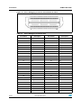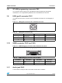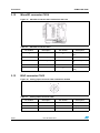
1
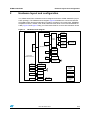
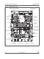
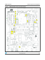
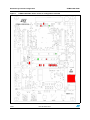
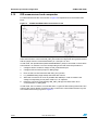
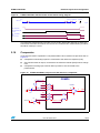
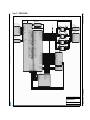
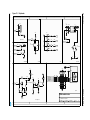
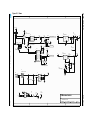
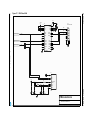
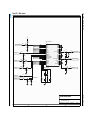
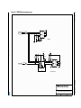
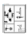
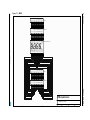
UM0684
User manual
STM8L1526-EVAL evaluation board
Introduction
The STM8L1526-EVAL evaluation board is a complete demonstration and development
platform for STMicroelectronic's STM8 core-based STM8L152C6 microcontroller which
supports I2C, SPI, USART, 12-bit ADC, 12-bit DAC, LCD driver, 2 KB internal SRAM, 32 KB
EEPROM and SWIM debugging.
The full range of hardware features on the board helps you evaluate all peripherals (motor
control, USART, audio DAC, LCD, IR LED, IrDA, SPI Flash, MicroSD Card, temperature
sensor and EEPROM… etc.) and develop your own applications. Extension headers
facilitate easy connection of a daughterboard or wrapping board for specific applications.
An ST-LINK is integrated on the board as the embedded in-circuit debugger and
programmer for the STM8 MCU.
Figure 1.
September 2009
STM8L1526-EVAL evaluation board
Doc ID 15437 Rev 1
1/46
www.st.com
Contents
STM8L1526-EVAL
Contents
1
2
3
2/46
Features . . . . . . . . . . . . . . . . . . . . . . . . . . . . . . . . . . . . . . . . . . . . . . . . . . . 4
1.1
Hardware . . . . . . . . . . . . . . . . . . . . . . . . . . . . . . . . . . . . . . . . . . . . . . . . . . 4
1.2
Demonstration software . . . . . . . . . . . . . . . . . . . . . . . . . . . . . . . . . . . . . . . 4
1.3
Order code . . . . . . . . . . . . . . . . . . . . . . . . . . . . . . . . . . . . . . . . . . . . . . . . . 4
Hardware layout and configuration . . . . . . . . . . . . . . . . . . . . . . . . . . . . . 5
2.1
Power supply . . . . . . . . . . . . . . . . . . . . . . . . . . . . . . . . . . . . . . . . . . . . . . . 8
2.2
Clock source . . . . . . . . . . . . . . . . . . . . . . . . . . . . . . . . . . . . . . . . . . . . . . . . 9
2.3
Reset source . . . . . . . . . . . . . . . . . . . . . . . . . . . . . . . . . . . . . . . . . . . . . . 10
2.4
LCD glass module . . . . . . . . . . . . . . . . . . . . . . . . . . . . . . . . . . . . . . . . . . 10
2.5
Audio . . . . . . . . . . . . . . . . . . . . . . . . . . . . . . . . . . . . . . . . . . . . . . . . . . . . 11
2.6
EEPROM . . . . . . . . . . . . . . . . . . . . . . . . . . . . . . . . . . . . . . . . . . . . . . . . . 12
2.7
RS-232 and IrDA . . . . . . . . . . . . . . . . . . . . . . . . . . . . . . . . . . . . . . . . . . . 12
2.8
Motor control . . . . . . . . . . . . . . . . . . . . . . . . . . . . . . . . . . . . . . . . . . . . . . 13
2.9
MicroSD Card . . . . . . . . . . . . . . . . . . . . . . . . . . . . . . . . . . . . . . . . . . . . . . 15
2.10
Analog input . . . . . . . . . . . . . . . . . . . . . . . . . . . . . . . . . . . . . . . . . . . . . . . 15
2.11
Serial Flash . . . . . . . . . . . . . . . . . . . . . . . . . . . . . . . . . . . . . . . . . . . . . . . 15
2.12
Temperature sensor . . . . . . . . . . . . . . . . . . . . . . . . . . . . . . . . . . . . . . . . . 15
2.13
Development and debug support . . . . . . . . . . . . . . . . . . . . . . . . . . . . . . . 16
2.14
Display and input devices . . . . . . . . . . . . . . . . . . . . . . . . . . . . . . . . . . . . . 17
2.15
IDD measurement and comparator . . . . . . . . . . . . . . . . . . . . . . . . . . . . . 18
2.16
Comparator . . . . . . . . . . . . . . . . . . . . . . . . . . . . . . . . . . . . . . . . . . . . . . . 19
2.17
IR LED . . . . . . . . . . . . . . . . . . . . . . . . . . . . . . . . . . . . . . . . . . . . . . . . . . . 20
Connectors . . . . . . . . . . . . . . . . . . . . . . . . . . . . . . . . . . . . . . . . . . . . . . . 21
3.1
RS-232 connector CN1 . . . . . . . . . . . . . . . . . . . . . . . . . . . . . . . . . . . . . . 21
3.2
Power connector CN2 . . . . . . . . . . . . . . . . . . . . . . . . . . . . . . . . . . . . . . . 21
3.3
TFT LCD connector CN3 . . . . . . . . . . . . . . . . . . . . . . . . . . . . . . . . . . . . . 21
3.4
Daughterboard extension connector CN4 and CN10 . . . . . . . . . . . . . . . . 22
3.5
LCD glass connector CN5 and CN6 . . . . . . . . . . . . . . . . . . . . . . . . . . . . . 24
3.6
Motor control connector CN7 . . . . . . . . . . . . . . . . . . . . . . . . . . . . . . . . . . 25
Doc ID 15437 Rev 1
STM8L1526-EVAL
4
Contents
3.7
STice connector CN8 . . . . . . . . . . . . . . . . . . . . . . . . . . . . . . . . . . . . . . . . 25
3.8
ST-LINK programming connector CN9 . . . . . . . . . . . . . . . . . . . . . . . . . . . 27
3.9
USB type B connector CN11 . . . . . . . . . . . . . . . . . . . . . . . . . . . . . . . . . . 27
3.10
SWIM connector CN12 and CN16 . . . . . . . . . . . . . . . . . . . . . . . . . . . . . . 27
3.11
Audio jack CN13 . . . . . . . . . . . . . . . . . . . . . . . . . . . . . . . . . . . . . . . . . . . . 27
3.12
MicroSD connector CN14 . . . . . . . . . . . . . . . . . . . . . . . . . . . . . . . . . . . . . 28
3.13
BNC connector CN15 . . . . . . . . . . . . . . . . . . . . . . . . . . . . . . . . . . . . . . . . 28
Schematics . . . . . . . . . . . . . . . . . . . . . . . . . . . . . . . . . . . . . . . . . . . . . . . 29
Appendix A STM8L1526-EVAL I/O assignment . . . . . . . . . . . . . . . . . . . . . . . . . . 43
Revision history . . . . . . . . . . . . . . . . . . . . . . . . . . . . . . . . . . . . . . . . . . . . . . . . . . . . 45
Doc ID 15437 Rev 1
3/46
Features
STM8L1526-EVAL
1
Features
1.1
Hardware
1.2
●
Three 5 V power supply options: power jack, ST-LINK USB connector or daughterboard
●
Audio speaker and microphone connected to the DAC and ADC of the STM8L152C6
●
1 GByte SPI interface MicroSD Card
●
128 Mbit SPI serial Flash
●
I2C compatible serial interface 64 KBit EEPROM and SMBusTemperature sensor
●
RS-232 communication
●
IrDA transceiver
●
Inductor motor control connector
●
SWIM debug support, ST-LINK embedded
●
122x32 dot matrix LCD connected to the SPI interface of the STM8L152C6
●
Joystick with 4-direction control and selector
●
Reset and User button
●
4 color LEDs and one bicolor LED
●
MCU consumption measurement circuit
●
LCD glass 28 x 4 segments (7 digits alpha numeric) connected to the LCD driver inside
the STM8L152C6
●
Extension connector for daughterboard or wrapping board
●
MCU voltage choice 3.3 V or adjustable from 1.65 V to 3.6 V
●
STice connector footprint
●
Board RoHS compliant (lead free)
Demonstration software
Demonstration software is preloaded in the board’s Flash memory for easy demonstration of
device peripherals in stand-alone mode. For more information and to download the latest
version available, please refer to STM8L1526-EVAL demonstration firmware available on
web: www.st.com/mcu.
1.3
Order code
To order the STM8L152C6 evaluation board, use the order code STM8L1526-EVAL.
4/46
Doc ID 15437 Rev 1
STM8L1526-EVAL
Hardware layout and configuration
The STM8L1526-EVAL evaluation board is designed around the STM8L1526C6T6 (48-pin
LQFP package). The hardware block diagram Figure 2 illustrates the connection between
the STM8L152C6 and the peripherals (LCD glass, dot matrix LCD, serial Flash, EEPROM,
temperature sensor, USART, IrDA, audio, MicroSD Card, Motor control and embedded STLINK). Figure 3 and Figure 4 help you locate these features on the actual evaluation board.
Figure 2.
Hardware block diagram
MicroSD
card
SPI
Dot Matrix
LCD
Voltage
translator
Serial Flash
RS232
transceiver
USART
LCD driver
2
Hardware layout and configuration
USART
DB9 connector
IrDA
transceiver
LCD Glass module
Joystick
GPIO
MC control
connector
LEDs
STM8L1526
STM8L1526C6T6
ADC
Potentiometer
Micro-Phone
Amplifier
GPIO
User Key
ADC
BNC connector
DAC
1.65V to 3.6V
adjustable
regulator
Audio DAC
3.3V regulator
EEPROM
MCU
consumption
measurement
I2C
Temperature
Sensor
SWIM
Embedded
ST-LINK
USB TypeB
connector
Doc ID 15437 Rev 1
Extension
connector for
GPIOs
5/46
Hardware layout and configuration
Figure 3.
STM8L1526-EVAL
STM8L1526-EVAL layout
CN4, CN10 Extension header
CN7 Motor control
U16
STM8L1526
CN8 STice
connector
LD6 IR LED
LCD
glass module
U2 IrDA
CN15 BNC
connector
CN1
USART
CN11 ST-LINK
USB connector
CN12 & CN13
SWIM connector
U7
Dot matrix LCD
CN14
MicroSD Card
CN2
Power Jack
CN13
Audio Jack
RV1
VDD_Adjustment
RV2 Potentiometer
6/46
B1 reset key
U17 joystick
Doc ID 15437 Rev 1
B2 user key
STM8L1526-EVAL
Figure 4.
Hardware layout and configuration
STM8L1526-EVAL jumpers and solder bridges
Doc ID 15437 Rev 1
7/46
Hardware layout and configuration
2.1
STM8L1526-EVAL
Power supply
The STM8L1526-EVAL is designed to be powered by a 5 V DC power supply and to be
protected by PolyZen from a wrong power plug-in event. It is possible to configure the
evaluation board to use any of following three power supply sources.
1.
5 V DC power adapter connected to CN2, the power jack on the board (power supply
unit (PSU) on silk screen).
●
5 V DC power with 500 mA limitation from CN11, the USB type B connector for STLINK (ST-link on silkscreen (STL)).
●
5 V DC power from CN10, the extension connector for daughterboard (daughterboard
power source (DTB) on silkscreen).
The power supply is configured by setting the related jumpers JP1, JP2 and JP11 as
described in Table 1.
Table 1.
Jumper
Power related jumpers: JP1, JP2, JP11
Description
STLink
DTB
PSU
JP2 selects one of the three possible power supply resources.
For power supply jack(CN2) to the STM8L1526-EVAL only, JP2 is set as shown
to the right.
Setting
For power supply from the daughterboard connectors(CN10) to STM8L1526EVAL only, JP2 is set as shown to the right.
STLink
DTB
PSU
For power supply from ST-LINK connector (CN11) to STM8L1526-EVAL only,
JP2 is set as shown to the right (default setting).
STLink
DTB
PSU
JP2
STLink
DTB
PSU
For power supply from power supply jack (CN2) to both STM8L1526-EVAL and
daughterboard connected on CN4 and CN10, JP2 is set as shown to the right
(daughterboard must not have its own power supply connected).
VDD is connected to fixed +3.3 V DC power when JP1 is set as shown to the
right (default setting).
1 2 3
VDD is connected to adjustable DC power from 1.65 V to 3.6 V when JP1 is set
as shown to the right.
1 2 3
VDD power is directly connected to MCU VDD when JP11 is set as shown to
the right.
Note: For manual IDD measurement the jumper on JP11 must be removed and
replaced by an ammeter connected between JP11 pin 2 and pin 3.
1 2 3
Connect VDD power to MCU with current-sampling resistor, 2 ohm or 2 Kohm,
in-series for IDD current measurement when JP11 is set as shown to the right
(default setting).
1 2 3
JP1
JP11
8/46
Doc ID 15437 Rev 1
STM8L1526-EVAL
Hardware layout and configuration
To enable MCU power consumption measurement, JP11, JP3 and LCD glass module
should be re-configured as described in Table 1 and Table 2.
Table 2.
MCU power consumption measurement related jumpers
Jumper
Description
The microphone output is connected to ADC of the STM8L152C6 when JP3 is closed.
Default setting: Fitted
For MCU power consumption measurement, JP3 must be kept open to avoid current
injection.
For motor control application, JP3 must be kept open to avoid conflict between the
speaker and motor control connector, CN7.
JP3
LCD glass The LCD glass module must be mounted on the "IO" position for MCU power
module
consumption measurement. Refer to Section 2.4: LCD glass module for details.
The LED LD8 is lit when the STM8L1526-EVAL evaluation board is powered by the 5 V
correctly, the LED LD9 is lit if the MCU is powered by a low voltage (VDD < 1.8 V).
Note:
The AC220V to DC5V power adapter PSU-5V2A (recommended, can be ordered from ST, it
is not provided with board by default) or equivalent (polarity compatible with CN2) can be
used to power the STM8L1525-EVAL board via the power jack CN2 on the board.
To order the recommended power supply, use the order code PSU-5V2A.
2.2
Clock source
Two clock sources are available on the STM8L1526-EVAL for the STM8L152C6 and
embedded RTC.
●
X2, 32 kHz crystal for embedded RTC
●
X1, 16 MHz crystal with socket for the STM8L152C6 microcontroller, it can be removed
from the socket when the internal RC clock is used.
Table 3.
32 kHz crystal X2 related solder bridges
Solder bridge
Description
PC5 is connected to 32 kHz crystal when SB3 is set as pad1 connected to pad2
(default setting).
SB3
PC5 is connected to STice connector CN8 and extension connector CN4 when SB3
is set as pad2 connected to pad3.
PC6 is connected to 32 kHz crystal when SB4 is set as pad2 connected to pad3
(default setting).
SB4
PC6 is connected to STice connector CN8 and extension connector CN4 when SB4
is set as pad1 connected to pad2.
Note:
I/O ports PA2 and PA3 can be used as GPIO on extension connector by closing solder
bridges SB1 and SB2 when crystal X1 is removed from it's socket.
Doc ID 15437 Rev 1
9/46
Hardware layout and configuration
2.3
STM8L1526-EVAL
Reset source
The reset signal of the STM8L1526-EVAL is low active and the reset sources include:
●
Reset button B1
●
Debugging tools from SWIM connector CN12 and CN16
●
Daughterboard from CN10
●
Embedded ST-LINK
●
RS-232 connector CN1 for ISP
Table 4.
Reset related jumpers
Jumper
2.4
Description
Setting
JP15
The board Reset is managed by pin 1 of connector CN1 (RS-232 DCD signal)
when JP15 is closed. This configuration is used for boot loader application only.
Default Setting: Not fitted
JP13
PA1 is connected to the Reset source listed above when JP13 is set as shown to
the right: (Default setting).
1 2 3
PA1 is connected to ground when JP13 is set as shown to the right. So, the MCU
is kept on Reset when you connect STice to CN8 for debugging.
1 2 3
LCD glass module
An LCD glass module (MB821) with 8-digit liquid crystal display is mounted on the
STM8L1526-EVAL evaluation board. It can be connected to the LCD driver of the
STM8L152C6 MCU or can work as a set of jumpers by mounting it in two possible positions,
position IO or position LCD.
●
Position IO. All peripherals (USART, IrDA, MicroSD Card, dot matrix LCD, serial Flash,
LEDs, joystick, bicolor LED, potentiometer, MCU consumption measurement, motor
control and microphone) shared with LCD glass are connected to the STM8L152C6
and the LCD glass is disconnected when LCD glass module is mounted on position IO
as shown below (default setting). See Figure 5.
●
Position LCD. LCD glass is connected to the LCD driver of the STM8L152C6 and all
peripherals shared with the LCD glass are disconnected when the LCD glass module is
mounted on position LCD as shown below. In this position, as well as the LCD, there
are other resources available on the board:
–
I2C EEPROM or Key button depending on JP7 jumper position
–
Audio speaker amplifier or BNC depending on JP10 jumper position.
–
IR LED depending on JP6 jumper position.
See Figure 6.
10/46
Doc ID 15437 Rev 1
STM8L1526-EVAL
2.5
Hardware layout and configuration
Figure 5.
LCD glass module in position I/O
Figure 6.
LCD glass module in position LCD
Audio
The STM8L1526-EVAL supports:
●
a speaker connected to the DAC output of the STM8L152C6 through an audio amplifier
which can be enabled or disabled by setting JP9. The choice between BNC or DAC
output on PF0 is done by JP10, refer to Table 5 for details.
●
a microphone connected to the ADC input of the STM8L152C6 through a microphone
amplifier. The microphone output can be connected or disconnected to the
STM8L152C6 by setting JP3 to closed or open, refer to Table 2 for details.
Table 5.
Jumper
JP9
Audio related jumpers
Description
Setting
The speaker amplifier is enabled when JP9 is closed.
Default setting: Fitted
PF0 is connected to BNC connector CN15 when JP10 is set as shown to the
right.
1 2 3
PF0 is connected to speaker when JP10 is set as show to the right (default
setting).
1 2 3
JP10
The LCD glass module must be mounted on "IO" position for Microphone. Refer to
Section 2.4: LCD glass module for details.
Doc ID 15437 Rev 1
11/46
Hardware layout and configuration
2.6
STM8L1526-EVAL
EEPROM
A 64 KBit EEPROM is connected to the I2C bus of the STM8L152C6.
Table 6.
EEPROM related jumpers
Jumper
JP14
Description
Setting
The I2C EEPROM U29 is in write protection mode when JP14 is not fitted.
Default setting: Fitted
PC1 is connected to the User button when JP7 is set as shown to the right .
1 2 3
PC1 is connected to I2C_SCL when JP7 is set as shown to the right (default
setting).
1 2 3
JP7
Note:
The E2PROM used on the board (ref M24C64-DFW5TP) is limited in VDD range from 1.7 to
5.5 V by specification therefore its behavior is not guaranteed for VDD from 1.65 to 1.7 V.
2.7
RS-232 and IrDA
Both RS-232 and IrDA communication is supported by D-type 9-pin RS-232 connectors
CN1 and IrDA transceiver U2 which connect to the USART of the STM8L152C6 on the
STM8L1526-EVAL evaluation board.
The signal Bootloader_RESET is added on the RS-232 connector for ISP support.
RS-232 or IrDA can be selected by setting JP5.
Table 7.
Jumper
RS-232 and IrDA related jumper
Description
Setting
USART_RX is connected to the RS-232 transceiver and RS-232 communication
is enabled when JP5 is set as shown to the right (default setting).
1 2 3
USART_RX is connected to the IrDA transceiver and IrDA communication is
enabled when JP5 is set as shown to the right.
1 2 3
JP5
The LCD glass module must be mounted in the IO position for RS-232 and IrDA. Refer to
Chapter 2.4: LCD glass module for details.
Note:
12/46
Hardware flow control is not supported by the RS-232 interface (CTS and RTS not managed
by MCU).
Doc ID 15437 Rev 1
STM8L1526-EVAL
2.8
Hardware layout and configuration
Motor control
The STM8L1526-EVAL supports three-phase brushless motor control via a 34-pin
connector, CN7, which provides all required control and feedback signals to and from motor
power-driving board. Available signals on this connector include emergency stop, motor
speed, 3 phase motor current, bus voltage, heat sink temperature coming from the motor
driving board and 6 channels of PWM control signal going to the motor driving circuit.
The I/O pins used on the motor control connector, CN7, are multiplexed with some
peripherals on the board. The motor control application can be enabled by setting jumpers
JP3, JP4 and JP8.
Table 8.
Jumper
Motor control related jumpers
Description
JP4
JP4 redirects the PFC synchronization signal to the timer 3 input capture 2 pin, additionally
to the timer3 external trigger input.
Default setting: Not Fitted.
JP8
JP8 should be kept open when the encoder signal is input from pin31 of CN7.
JP8 should be kept closed when analog signal is from pin31 of CN7 for special motor.
Default setting: Not Fitted.
JP3
For motor control application, JP3 must be kept open to avoid conflict between speaker
and motor control connector, CN7.
Some rework that is required to be done to the board is listed below:
●
Remove 0 ohm resistors, R69, R75,R80,R58,R35,R42,R31,R34,R62,R39,R55 and
R48 (all resistors are marked in red in Figure 7) to release I/Os used by motor control
and shared with another peripherals.
●
Remove MicroSD Card from SD Card socket CN14 (SD Card socket is marked in red in
Figure 7).
●
Solder resistor R82 (0 ohm), R59 (0 ohm) and R29 (0 ohm), all components to be
soldered are marked in green in Figure 7.
The LCD glass module has to be mounted in the IO position for motor control. Refer to
Section 2.4: LCD glass module for details.
Doc ID 15437 Rev 1
13/46
Hardware layout and configuration
Figure 7.
14/46
STM8L1526-EVAL
STM8L1526-EVAL motor control re-configuration of board
Doc ID 15437 Rev 1
STM8L1526-EVAL
2.9
Hardware layout and configuration
MicroSD Card
The 1 GByte MicroSD Card connected to the SPI port of the STM8L152C6 is available on
the board. MicroSD Card detection is managed by standard I/O port, PD6.
The LCD glass module must be mounted in the IO position for MicroSD Card. Refer to
Chapter 2.4: LCD glass module for details.
2.10
Analog input
The BNC connector, CN15, is connected to PF0 of the STM8L152C6 as an external analog
input or DAC output. The 50 ohm terminal resistor can be enabled by closing solder bridge
SB6. A low-pass filter can be implemented for the BNC connector by replacing R126 and
C86 for ADC input or replacing R127 and C86 for DAC output (with suitable resistor and
capacitor as requested by end user's application).
There are also 3 analog signals available on the board.
1.
10 Kohm potentiometer RV2 connected to PC7.
2.
IDD measurement output signal connected to PD3 for MCU power consumption test.
3.
External ADC input which can be connected to TP8 (AIN+) and TP5 (AIN-). Solder
bridge SB5 should be kept on open for this analog input.
The LCD glass module has to be mounted in the IO position for IDD measurement and
potentiometer RV2. Refer to Section 2.4: LCD glass module for details.
2.11
Serial Flash
The M25P128 serial Flash is connected to the SPI bus of the STM8L152C6. The chip select
is managed by standard I/O port, PE4.
The LCD glass module has to be mounted in the IO position for serial Flash. Refer to
Section 2.4: LCD glass module for details.
2.12
Temperature sensor
A temperature sensor STLM75M2E is connected to the I2C bus of the STM8L152C6
through two transistors to support a wide voltage range from 1.8 V to 3.3 V on the I2C bus.
A voltage lower than 1.8 V is not supported due to the VGS threshold of transistor TR1 and
TR2.
The LCD glass module has to be mounted in the IO position for the I2C_SMB signal. Refer
to Section 2.4: LCD glass module for details.
Doc ID 15437 Rev 1
15/46
Hardware layout and configuration
2.13
STM8L1526-EVAL
Development and debug support
An embedded ST-LINK, STM8 debugger developed by STMicroelectronics, is available on
the STM8L1526-EVAL as the default debugger. Third-party debuggers are also supported
by the SWIM connector, CN12, or low-cost SWIM connector, CN16.
The SWIM connector or embedded ST-LINK can be enabled by setting jumper JP6.
Table 9.
SWIM debugging related jumper
Jumper
Description
Setting
PA0 is connected to SWIM connector CN12, CN16 and embedded ST-LINK when
JP6 is set as shown to the right (default setting).
1 2 3
PA0 is connected to IR LED, LD6 when JP6 is set as show to the right.
1 2 3
JP6
A 60-pin connector CN8 is available also for STice user, it can be used even with MCU
silicon mounted on the board by setting jumper JP13. (The STice connector is available only
on the MB818 with an MCU socket).
Table 10.
Jumper
JP13
16/46
STice related jumper
Description
Setting
PA1 is connected to Reset sources when JP13 is set as shown to the right, the
board is working on standalone mode without STice connected (default setting).
1 2 3
PA1 is connected to GND when JP13 is set as show to the right. All I/Os of
STM8L152C6 silicon on the board is kept on "floating input" which allows
debugging based on STice connected to CN8.
1 2 3
Doc ID 15437 Rev 1
STM8L1526-EVAL
2.14
Hardware layout and configuration
Display and input devices
The 122x32 dot-matrix LCD connected to the SPI port of the STM8L152C6, 4 general
purpose color LED's (LD 1,2,3,4), and one bicolor LED LD5 are available as display devices.
The 4-direction joystick (U17) with selection key and general purpose button (B2) are
available as input devices.
The STM8L1526-EVAL evaluation board also supports a second optional 2.4" TFT LCD that
can be mounted on the CN3 connector. The 2.4" TFT LCD is not populated by default.
MB542 is the reference of the 2.4" TFT LCD to be connected on CN3.
)
Table 11.
LCD modules
122x32 dot-matrix LCD U7 (default)
Pin on U7 Description
Pin connection
2.4" TFT LCD CN3 (optional)
Pin on CN3 Description
Pin connection
1
Vss
GND
1
CS
PB4
2
Vcc
+3.3V
2
SCL
PB5
3
VO
-
3
SDI
PB6
4
CLK
PB5
4
RS
-
5
SID
PB6
5
WR
-
6
CS
PB4
6
RD
-
7
A
+5V
7
SDO
PB7
8
K
GND
8
RESET
RESET#
9
VDD
3.3V
10
VCI
3.3V
11
GND
GND
12
GND
GND
13
BL_VDD
3.3V
14
BL_Control
3.3V
15
BL_GND
GND
16
BL_GND
GND
The LCD glass module must be mounted on the "IO" position for LCD, LED's and joystick.
Refer to Section 2.4: LCD glass module for details.
Doc ID 15437 Rev 1
17/46
Hardware layout and configuration
2.15
STM8L1526-EVAL
IDD measurement and comparator
For IDD measurement the circuit shown in Figure 9 is implemented on the STM8L1526EVAL.
Figure 8.
STM8L1526-EVAL IDD measurement circuit
In Run mode, IDD current is measured using MAX9938FEUK+ (U20) connected to the
2ohm shunt resistor. In this case IDD_CNT_EN remains at a high level during measurement
and the jumper must be connected between pin 1 and pin 2 of JP11.
In Halt mode, the operational amplifier MAX9938FEUK+ (U20) is connected on the 2 Kohm
shunt resistor. To measure a current corresponding to the Halt mode the procedure is:
1.
Configure ADC to measure voltage on IDD_measurement pin.
2.
Configure PE6 as interrupt input on falling edge.
3.
Enter in Halt or active Halt mode with IDD_CNT_EN low.
4.
LP_WAKEUP falling edge wakeup the MCU after 150 ms.
5.
Start ADC conversion as soon as possible after wakeup in order to measure the
voltage corresponding to low power mode on 1 uF capacitor.
6.
Reset the counter by programming IDD_CNT_EN high to avoid 2 Kohm to be
connected later on VDD_MCU.
In Halt mode, the 2 K resistor is connected when T3 goes off after entering Halt mode. Q12
output of the counter allows connection of the 2 K when the current IDD becomes very low.
The measurement timing is given in Figure 9.
18/46
Doc ID 15437 Rev 1
STM8L1526-EVAL
Figure 9.
Hardware layout and configuration
STM8L1526-EVAL IDD Halt mode measurement timing diagram
Halt mode IDD measurement timing
Ru n
Wake-up
H alt
ID D Measure
C lear C N T
MC U mode
0
150mS
300mS
450mS
ID D_C NT_EN (PE7)
Q12= L OW _POW ER _EN
(T3 pin 3)
Q13 = LP_WAK EU P
(PE6)
Q13n = U21 p in 4
The Halt mode measurement procedure can be used in Halt mode and slow or fast active
Halt modes if the IDD current does not exceed 12 uA else the Run measurement procedure
should be used up to 12 mA.
Comparator
Three I/Os are used to implement a comparator feature to be used as low precision ADC in
Figure 10.
●
Comparator noninverting input PD1 connected to the reference capacitor (Cref).
●
One I/O PE0 used as output, connected to the reference resistor (Rref) used to charge
Cref.
●
Comparator inverting input used as ADC input PC7 to be connected to the
potentiometer.
1
2
COMP2
CMP_Rref PE0
PE5
Rref
COMP2A
PD0
4
2
Figure 10. STM8L1526-EVAL low precision ADC based on comparator
1
CMP_Cref PD1
12
GND
11
Cref
PC3
+
5
TIM2/3
6
2.16
PC4
PC7
P1
VDD_ADJ
1
2
10K
VREFINT 1.2V
GND
Doc ID 15437 Rev 1
19/46
Hardware layout and configuration
STM8L1526-EVAL
The measurement is performed in three steps:
2.17
1.
Internal reference voltage VREFINT is connected to the comparator inverting input and
Cref to noninverting input to measure the time required to charge the capacitor to
internal reference voltage VREFINT by PE0 used as output through Rref.
2.
The potentiometer is connected to inverting input to measure the time required to
charge Cref to the voltage on potentiometer.
3.
The potentiometer voltage is calculated by software interpolation or using a conversion
table.
IR LED
One IR LED, LD6, is driven by either PA0 through two transistors T1 and T8, or PA0 directly;
depending on the setting of the solder bridge SB7.
Table 12.
IR LED related solder bridges
Solder bridge
SB7
Description
LD6 is driven by PA0 through two transistors, T1 and T8, when SB7 is set as pad1
connected to pad2 (default setting).
LD6 is driven by PA0 directly when SB7 is set as pad2 connected to pad3.
Note:
20/46
JP6 needs to be set correspondingly for IR LED, please refer to Table 9 for details.
Doc ID 15437 Rev 1
STM8L1526-EVAL
Connectors
3
Connectors
3.1
RS-232 connector CN1
Figure 11. RS-232 connector CN1 with ISP support
Table 13.
RS-232 connector CN1 with ISP support
Pin number
3.2
Description
Pin number
Description
1
Bootloader_RESET
6
NC
2
RS232_RX (PC2)
7
NC
3
RS232_TX (PC3)
8
NC
4
NC
9
NC
5
GND
Power connector CN2
The STM8L1526-EVAL evaluation board can be powered from a DC 5 V power supply via
the external power supply jack (CN2) shown in Figure 12. The central pin of CN2 must be
positive.
Figure 12. Power supply connector CN2 viewed from front
DC+5V
GND
3.3
TFT LCD connector CN3
CN3 is used to support TFT color LCD board (MB542), it is not populated by default.
Doc ID 15437 Rev 1
21/46
Connectors
3.4
STM8L1526-EVAL
Daughterboard extension connector CN4 and CN10
Two 26-pin male headers CN4 and CN10 can be used to connect the daughterboard or
standard wrapping board to the STM8L1526-EVAL evaluation board. All GPI/Os are
available on it. The space between these two connectors and position of power, GND and
RESET pin are defined as a standard which allows to develop common daughterboards for
several evaluation boards. The standard width between CN4 pin1 and CN10 pin1 is
2700 mils (68.58mm). The standard was implemented on the majority of evaluation boards.
Each pin on CN4 and CN10 can be used by a daughterboard after disconnecting it from the
corresponding function block on the STM8L1526-EVAL evaluation board. Please refer to
Table 14 and Table 15 for details.
Table 14.
Daughterboard extension connector CN4
Pin Description
22/46
Alternative function
How to disconnect with function
block on STM8L1526-EVAL board
1
GND
-
3
PC5
32 kHz crystal
Set SB3 to 2<->3
5
PC7
Potentiometer
Remove R28
7
PD1
CMP_Cref / Motor control connector
(PFC sync)
Remove R35
9
PD3
IDD_Measurement
Remove R50
11
PA0
SWIM / IR_LED
Set JP6 to open
13
PA1
RESET button
Set JP13 to open
15
PA4
Remove R69
LED1 / Motor control connector (Current
Disconnect power driver board from
A)
Motor control connector
17
PA6
Remove R80
LED3 / Motor control connector (Current
Disconnect power driver board from
C)
Motor control connector
19
GND
-
21
PD5
Joystick_right / Motor control connector
(MC_WH)
Remove R34
Disconnect power driver board from
Motor control connector
23
PD7
Joystick_up / Motor control connector
(MC_UL)
Remove R31
Disconnect power driver board from
Motor control connector
25
PC1
I²C SDA
Set JP7 to open
2
PC4
I²C_SMB
Remove R27
4
PC6
32 kHz crystal
Set SB4 to 1<->2
6
PD0
Motor control connector (PFC sync)
Disconnect power driver board from
Motor control connector
8
PD2
Bicolor_LED / Motor control connector
(MC_UH)
Remove R48
Disconnect power driver board from
Motor control connector
Doc ID 15437 Rev 1
STM8L1526-EVAL
Table 14.
Connectors
Daughterboard extension connector CN4 (continued)
Pin Description
How to disconnect with function
block on STM8L1526-EVAL board
Alternative function
10
GND
-
12
PA2
16MHZ crystal
Set SB2 to close
Remove X1 and C30
14
PA3
16MHZ crystal
Set SB1 to close
Remove X1 and C38
16
PA5
LED2 / Motor control connector (Bus
voltage)
Remove R75
18
PA7
LED4 / Motor control connector
(Encoder index)
Remove R58
Disconnect power driver board from
Motor control connector
20
PD4
Remove R39
Joystick_down / Motor control connector
Disconnect power driver board from
(MC_VH)
Motor control connector
22
PD6
Motor control connector
(EmergencySTOP) / SDcard_detect
Remove SD Card from card socket
24
PC0
I²C SDA
Remove R115
26
PC2
UART_IrDA_RX
Set JP5 to open
Table 15.
Daughterboard extension connector CN10
Pin Description
Alternative function
How to disconnect with component
on STM8L1526-EVAL board
1
GND
-
-
3
PB1
Motor control connector (Dissipative
brake & PFC PWM)
Disconnect power driver board from
Motor control connector
5
PB3
Audio_ADC_IN
Set JP3 to open
7
PB5
LCD_SDcard_Flash_SCK
-
9
PB7
LCD_SDcard_Flash_MISO
Remove R73 and SD Card from card
socket
11
RESET#
13
PE1
Joystick_Left / Motor control connector
(MC_VL)
Remove R62
Disconnect power driver board from
Motor control connector
15
PE3
Micro SD card_CS
Remove SD Card from card socket
17
PE5
Motor control connector (MC_CurrentB)
Disconnect power driver board from
Motor control connector
19
D5V
-
-
21
NC
-
-
23
NC
-
-
-
Doc ID 15437 Rev 1
23/46
Connectors
STM8L1526-EVAL
Table 15.
Daughterboard extension connector CN10 (continued)
Pin Description
Alternative function
How to disconnect with component
on STM8L1526-EVAL board
25
PF0
Motor control connector (Current B) /
BNC / Audio_DAC_out
Set JP10 to open
2
PB0
Motor control connector (Encoder A)
Disconnect power driver board from
Motor control connector
4
PB2
Motor control connector (Encoder B)
Disconnect power driver board from
Motor control connector
6
PB4
Dot-matrix LCD_CS
Remove Dot-Matrix LCD module
8
PB6
LCD_SDcard_Flash_MOSI
-
10
GND
-
-
12
PE0
CMP_Rref / Motor control connector
(NTC_bypass)
Remove R42
Disconnect power driver board from
Motor control connector
14
PE2
Joystick_sel / Motor control connector
(MC_WL)
Remove R55
Disconnect power driver board from
Motor control connector
16
PE4
Serial Flash_CS
Remove R73
18
PE6
IDD_Measurement_Wakeup
Remove LCD glass module (MB821)
0ohm resistor to be added?
20
PE7
IDD_Measurement_CNT_EN
-
22
PC3
UART_IrDA_TX
-
24
MCU_VDD
-
26
NC
-
Note:
All I/O's marked in grey can be disconnected with function block on the STM8L1526-EVAL
board by removing LCD glass module (MB821) board.
3.5
LCD glass connector CN5 and CN6
Two 36-pin male headers, CN5 and CN6, can be used to mount the LCD glass module
(MB821) on it. Two possible mount positions may be selected by the user for either an LCD
glass demonstration or other peripherals on STM8L1526-EVAL board.
24/46
Doc ID 15437 Rev 1
STM8L1526-EVAL
3.6
Connectors
Motor control connector CN7
Figure 13. Motor control connector CN7 viewed from above
33 31 29 27 25 23 21 19 17 15 13 11 9 7
34 32 30 28 26 24 22 20 18 16 14 12 10 8
Viewed from above
Table 16.
Motor control connector CN7
Description
3.7
Pin of
Pin of
CN17 pin CN17 pin
STM8L152C6
STM8L152C6
Description
EMERGENCY STOP
PD6
1
2
GND
PWM-UH
PD2
3
4
GND
PWM-UL
PD7
5
6
GND
PWM-VH
PD4
7
8
GND
PWM-VL
PE1
9
10
GND
PWM-WH
PD5
11
12
GND
PWM-WL
PE2
13
14
PHASE A CURRENT
PA4
15
16
GND
PHASE B CURRENT
PE5
17
18
GND
PHASE C CURRENT
PA6
19
20
GND
NTC BYPASS RELAY
PE0
21
22
GND
DISSIPATIVE BRAKE
PWM
PB1
23
24
GND
+5V power
+5V
25
26
PFC SYNC
PD0 and PD1
27
28
VDD_Micro
PFC PWM
PB1
29
30
GND
Encoder A
PB0
31
32
GND
Encoder B
PB2
33
34
PA5
PB3
PA7
BUS VOLTAGE
Heatsink temperature
Encoder Index
STice connector CN8
The STice can be connected to emulate the STM8L1526-EVAL board. Jumper JP13 must
be set to connect pin 2 and 3 when the STice is connected on CN8. It is used to keep the
STM8L152C6 MCU on reset as explained in Section 2.3: Reset source.
Doc ID 15437 Rev 1
25/46
Connectors
STM8L1526-EVAL
Figure 14. STice debugging connector CN8 viewed from above
Table 17.
1
59
2
60
STice debugging connector CN8
Pin number
26/46
Description
Pin number
Description
1
PA0
2
RESET#
3
PA2
4
PA3
5
PA4
6
PA5
7
PA6
8
PA7
9
GND
10
VDD_MCU
11
VDDA
12
VDDA
13
VLCD
14
PE0
15
PE1
16
PE2
17
PE3
18
PE4
19
PE5
20
PD0
21
PD1
22
PD2
23
PD3
24
PB0
25
PB1
26
PB2
27
PB3
28
PB4
29
PB5
30
PB6
31
PB7
32
PF0
33
PD4
34
PD5
35
PD6
36
PD7
37
PC0
38
PC1
39
VDD_MCU
40
GND
41
PC2
42
PC3
43
PC4
44
PC5
45
PC6
46
PC7
47
PE6
48
PE7
49-60
NC
Doc ID 15437 Rev 1
STM8L1526-EVAL
3.8
Connectors
ST-LINK programming connector CN9
The connector CN9 is used only for embedded ST-LINK programming during board
manufacture. It is not populated by default and is not intended for the end user.
3.9
USB type B connector CN11
The USB connector CN11 is used to connect embedded ST-LINK to PC for debugging of
board.
Figure 15. USB type B connector CN11 viewed from the front
Table 18.
USB type B connector CN11
Pin number
3.10
Description
1
VBUS(power)
2
DM
3
DP
Pin number
Description
4
GND
5,6
Shield
SWIM connector CN12 and CN16
Figure 16. SWIM debugging connector CN16 viewed from the above
1
Table 19.
3
4
SWIM debugging connector CN12 and CN16
Pin number
3.11
2
Description
Pin number
Description
1
VDD
2
SWIM line (PA0)
3
GND
4
RESET#
Audio jack CN13
A 3.5mm stereo audio jack CN13 connected to audio DAC is available.
Doc ID 15437 Rev 1
27/46
Connectors
3.12
STM8L1526-EVAL
MicroSD connector CN14
Figure 17. MicroSD connector CN14 viewed from the front
Table 20.
MicroSD connector CN14
Pin number
Description
Pin number
1
5
MicroSDcard_CLK
(PB5)
2
MicroSDcard_CS (PE3)
6
Vss/GND
3
MicroSDcard_DIN(PB6
)
7
MicroSDcard_DOUT(P
B7)
4
+3V3
8
9
3.13
Description
MicroSDcard_detect
(PD6)
BNC connector CN15
Figure 18. Analog input connector CN15 viewed from bottom
1
2
5
4
Table 21.
Analog input connector CN15
Pin number
28/46
3
Description
Pin number
Description
1
GND
4
GND
2
GND
5
Analog input PF0
3
GND
Doc ID 15437 Rev 1
STM8L1526-EVAL
4
Schematics
Schematics
The schematics are shown on the following pages:
●
Table 19: STM8L1526-EVAL on page 30
●
Table 20: MCU on page 31
●
Table 21: LCD glass connector on page 32
●
Table 22: Audio on page 33
●
Table 23: Peripherals on page 34
●
Table 24: Power on page 35
●
Table 25: Extension and STice on page 36
●
Table 26: LCD and SD Card on page 37
●
Table 27: RS-232 and IrDA on page 38
●
Table 28: Motor control on page 39
●
Table 29: EEPROM and temperature sensor on page 40
●
Table 30: ST_LINK (SWIM only) on page 41.
●
Table 31: MB821 on page 42
Doc ID 15437 Rev 1
29/46
U_MCU
MCU.SchDoc
ST_LINK_SWIM
RESET#
I2C_SMB
U_LCD_Glass
LCD_Glass.SCHDOC
Doc ID 15437 Rev 1
PA4_LCDCOM0
PA5_LCDCOM1
PA6_LCDCOM2
PD1_LCDCOM3
PA7_LCDSEG0
PE0_LCDSEG1
PE1_LCDSEG2
PE2_LCDSEG3
PE3_LCDSEG4
PE4_LCDSEG5
PE5_LCDSEG6
PD0_LCDSEG7
PD2_LCDSEG8
PD3_LCDSEG9
PB0_LCDSEG10
PB1_LCDSEG11
PB2_LCDSEG12
PA4_LCDCOM0
PA5_LCDCOM1
PA6_LCDCOM2
PD1_LCDCOM3
PA7_LCDSEG0
PE0_LCDSEG1
PE1_LCDSEG2
PE2_LCDSEG3
PE3_LCDSEG4
PE4_LCDSEG5
PE5_LCDSEG6
PD0_LCDSEG7
PD2_LCDSEG8
PD3_LCDSEG9
PB0_LCDSEG10
PB1_LCDSEG11
PB2_LCDSEG12
PB4_LCDSEG14
PB5_LCDSEG15
PB6_LCDSEG16
PB7_LCDSEG17
PD4_LCDSEG18
PD5_LCDSEG19
PD6_LCDSEG20
PD7_LCDSEG21
PC2_LCDSEG22
PC3_LCDSEG23
PC4_LCDSEG24
PC7_LCDSEG25
PE6_LCDSEG26
PE7_LCDSEG27
PB4_LCDSEG14
PB5_LCDSEG15
PB6_LCDSEG16
PB7_LCDSEG17
PD4_LCDSEG18
PD5_LCDSEG19
PD6_LCDSEG20
PD7_LCDSEG21
PC2_LCDSEG22
PC3_LCDSEG23
PC4_LCDSEG24
PC7_LCDSEG25
PE6_LCDSEG26
PE7_LCDSEG27
C40
VDD U11
1
100nF
VCCA VCCB
R32 0 2
A1
B1
R37 0 3
A2
B2
4
GND
DIR
VDD
Audio_IN
R124
10K
Audio_IN
I2C_SMB
RS232/IrDA_RX
SPI_MISO
SDcard_detect
RS232/IrDA_TX
MicroSD_CS
SPI_SCK
SPI_MOSI
LCD_CS
Flash_CS
+3V3
8
7
6
5
C34
100nF
U_RS232_IrDA
RS232_IrDA.SCHDOC
Bootloader_RESET
RS232/IrDA_RX
RS232/IrDA_TX
U_LCD_MicroSD_Flash
LCD_MicroSD_Flash.SchDoc
SN74LVC2T45DCUT
C33
VDD U10
100nF
1
VCCA VCCB
2
A1
B1
3
A2
B2
4
GND
DIR
C24
100nF
SN74LVC2T45DCUT VDD
+3V3
U26
8
VCCA VCCB
7
A1
B1
6
A2
B2
5
GND
DIR
C65
100nF
SN74LVC2T45DCUT VDD
C69
VDD U22
+3V3
100nF
1
8
VCCA VCCB
2
7
A1
B1
3
6
A2
B2
4
5
GND
DIR
C74
100nF
C76
VDD
100nF
1
2
3
4
U_Peripherals
Peripherals.SchDoc
LED4
LED3
LED1
LED2
BiD_LED
CMP_Rref
CMP_Cref
JOY_UP
JOY_RIGHT
JOY_LEFT
JOY_DOWN
JOY_SEL
Potentiometer
+3V3
8
7
6
5
LED4
LED3
LED1
LED2
BiD_LED
CMP_Rref
CMP_Cref
JOY_UP
JOY_RIGHT
JOY_LEFT
JOY_DOWN
JOY_SEL
Potentiometer
SPI_MISO
SDcard_detect
MicroSD_CS
SPI_SCK
SPI_MOSI
LCD_CS
Flash_CS
RESET#
SN74LVC2T45DCUT VDD
User_Button
BNC
IR_LED
U_Power
Power.SchDoc
IDD_Measurement
LP_WAKEUP
IDD_CNT_EN
IDD_Measurement
LP_WAKEUP
IDD_CNT_EN
U_MotorControl
MotorControl.SCHDOC
R52
0
R40
[N/A]
MC_HeatsinkTemperature
MC_DissipativeBrake
MC_PFCpwm
MC_PFCsync1
MC_EnA
MC_EnB
MC_CurrentB
MC_EnIndex
MC_CurrentC
MC_CurrentA
MC_BusVoltage
MC_UH
MC_NTC
MC_PFCsync 2
MC_UL
MC_WH
MC_VL
MC_VH
MC_WL
MC_EmergencySTOP
ST_LINK_SWIM
RESET#
Audio_OUT
PB3_LCDSEG13
U_ST_LINK
ST_LINK.SCHDOC
I2C_SLK
I2C_SDA
U_Audio
Audio.SchDoc
MC_CurrentB
MC_EnB
MC_EnA
MC_PFCsync 1
MC_PFCpwm
EX_PC5
EX_PC6
Audio_OUT
User_Botton
IR_LED
BNC
PC[0..7]
PF0
PB[0..7]
PD[0..7]
PE[0..7]
PA[0..7]
I2C_SLK
I2C_SDA
PB3_LCDSEG13
PC[0..7]
PF0
PB[0..7]
PD[0..7]
PE[0..7]
PA[0..7]
RESET#
EX_PC5
EX_PC6
U_EEPROM_TemSensor
EEPROM_TemSensor. SCHDOC
Bootloader_RESET
U_Extension_STice connector
Extension_STice connector. SCHDOC
Schematics
30/46
Figure 19. STM8L1526-EVAL
STMicroelectronics
Title:
STM8L1526-EVAL
Number: MB818
Rev: C.1(PCB.SCH) Date: 7/31/2009
Sheet 1
of
STM8L1526-EVAL
Note: All text in the each sheet is in Italic format to be different with Net label.
2
3
1
2
3
4
20pF
PA4_LCDCOM0
PA5_LCDCOM1
PA6_LCDCOM2
PA7_LCDSEG0
X1
16MHz (with socket)
C38
R26
60
VDD_MCU
VDDA
20pF
VLCD
C60
1uF
PE0
PE1
PE2
PE3
PE4
PE5
PD0
PD1
PD2
PD3
PB0
PE0_LCDSEG1
PE1_LCDSEG2
PE2_LCDSEG3
PE3_LCDSEG4
PE4_LCDSEG5
PE5_LCDSEG6
PD0_LCDSEG7
PD1_LCDCOM3
PD2_LCDSEG8
PD3_LCDSEG9
PB0_LCDSEG10
TP9
PA0
PA1
PA2
PA3
PA4
PA5
PA6
PA7
AVSS
VDD
VDDA
VREF+
VLCD
PE0
PE1
PE2
PE3
PE4
PE5
PD0
PD1
PD2
PD3
PB0
PE7
PE6
PC7
PC6
PC5
PC4
PC3
PC2
VSSIO
VDDIO
PC1
PC0
PD7
PD6
PD5
PD4
PF0
PB7
PB6
PB5
PB4
PB3
PB2
PB1
48
47
46
45
44
43
42
41
40
39
38
37
36
35
34
33
32
31
30
29
28
27
26
25
PE7
PE6
PC7
PC6
PC5
PC4
PC3
PC2
PC1
PC0
PD7
PD6
PD5
PD4
PF0
PB7
PB6
PB5
PB4
PB3
PB2
PB1
PE7_LCDSEG27
PE6_LCDSEG26
PC7_LCDSEG25
User_Botton
I2C_SLK
PC4_LCDSEG24
PC3_LCDSEG23
PC2_LCDSEG22
1
Doc ID 15437 Rev 1
C30
1
2
3
4
5
6
7
8
9
10
11
12
13
14
15
16
17
18
19
20
21
22
23
24
SB3
solder bridge
CCO
U16
PA0
PA1
PA2
PA3
PA4
PA5
PA6
PA7
1
SB4
solder bridge
609-1306-ND(2.54mm)
SWIM connector
4
1
B1
RESET (Black)
ST_LINK_SWIM
2
C82
100nF
3
3
JP6
JP15
Bootloader_RESET
IR_LED
2
3
3
3
D1
BAT60
2
2
3
C25
6.8pF
4
MC306-G-06Q-32.768 (manufacturer JFVNY)
1
RESET#
1
1
2
214017
SWIM connector
CN12
JP13
1
C32
6.8pF
2
R111 0
R117
10K
X2
1
2
3
4 0
VDD
RESET#
EX_PC5
EX_PC6
CN16
3
VDD
4
2
1
STM8L1526-EVAL
Figure 20. MCU
VDD_MCU
JP7
I2C_SDA
PD7_LCDSEG21
PD6_LCDSEG20
PD5_LCDSEG19
PD4_LCDSEG18
3
Audio_OUT
2
1
PB7_LCDSEG17
PB6_LCDSEG16
PB5_LCDSEG15
PB4_LCDSEG14
PB3_LCDSEG13
PB2_LCDSEG12
PB1_LCDSEG11
JP10
TP8
AIN+
R127
0 R126
SB5
0
BNC
STM8L152C6T6
C86
[N/A]
VDD_MCU
C53
1uF
C61
100nF
C48
1uF
close to PF0 of MCU
C51
100nF
PA[0..7]
PB[0..7]
PC[0..7]
PD[0..7]
PE[0..7]
PF0
STMicroelectronics
Title:
31/46
STM8L1526-EVAL MCU
Number:MB818
1
2
3
Rev: C.1(PCB.SCH)
Date: 7/31/2009
4
Sheet 2 of
Schematics
PA[0..7]
PB[0..7]
PC[0..7]
PD[0..7]
PE[0..7]
PF0
C31
100nF
VDDA
L1
BEAD
TP5
AIN-
Schematics
32/46
Figure 21. LCD glass connector
CN5
Doc ID 15437 Rev 1
PC4_LCDSEG24
PC7_LCDSEG25
PD6_LCDSEG20
PD7_LCDSEG21
PB6_LCDSEG16
PB7_LCDSEG17
PB2_LCDSEG12
PB3_LCDSEG13
PD2_LCDSEG8
PD3_LCDSEG9
PE3_LCDSEG4
PE4_LCDSEG5
PA7_LCDSEG0
PE0_LCDSEG1
PD1_LCDCOM3
PA6_LCDCOM2
1
3
5
7
9
11
13
15
17
19
21
23
25
27
29
31
33
35
S28
2
S29
4
S24
6
S25
8
S20
10
S21
12
S16
14
S17
16
S12
18
S13
20
S8
22
S9
24
S4
26
S5
28
S0
30
S1
32
COM4 34
COM3 36
I2C_SMB
Potentiometer
SDcard_detect
JOY_UP
SPI_MOSI
SPI_MISO
MC_EnB
Audio_IN
BiD_LED
IDD_Measurement
MicroSD_CS
Flash_CS
LED4
CMP_Rref
CMP_Cref
LED3
Header 18X2
CN6
PE7_LCDSEG27
PE6_LCDSEG26
PC3_LCDSEG23
PC2_LCDSEG22
PD5_LCDSEG19
PD4_LCDSEG18
PB5_LCDSEG15
PB4_LCDSEG14
PB1_LCDSEG11
PB0_LCDSEG10
PD0_LCDSEG7
PE5_LCDSEG6
PE2_LCDSEG3
PE1_LCDSEG2
PA4_LCDCOM0
PA5_LCDCOM1
1
3
5
7
9
11
13
15
17
19
21
23
25
27
29
31
33
35
S31
2
S30
4
S27
6
S26
8
S23
10
S22
12
S19
14
S18
16
S15
18
S14
20
S11
22
S10
24
S7
26
S6
28
S3
30
S2
32
COM1 34
COM2 36
IDD_CNT_EN
LP_WAKEUP
RS232/IrDA_TX
RS232/IrDA_RX
JOY_RIGHT
JOY_DOWN
SPI_SCK
LCD_CS
MC_PFCpwm
MC_EnA
MC_PFCsync1
MC_CurrentB
JOY_SEL
JOY_LEFT
LED1
LED2
Header
Title:
STM8L1526-EVAL LCD Glass connector
Number:MB818
Rev: C.1(PCB.SCH)
Date: 7/31/2009
Sheet 3 of
STM8L1526-EVAL
STMicroelectronics
STM8L1526-EVAL
Figure 22. Audio
C45
Speaker+3V3
JP9
Audio_OUT
PF0
R38
R30
10K
R33
22K
470nF
C47
[N/A]
1
10
2
22K
U15
1
4
3
2
C43
0
2
1
CN13
330pF
R36
C37
1uF
Standby
VINVIN+
Bypass
VOUT1
VOUT2
VCC
GND
5
8
6
7
TS4990IST
U24
KDMG15008-03
ST-613
Speaker+
+3V3
C28
1uF
C12
R15
1K
U4
KECG2740TBL
2
1
10uF
R12
100
R11
2.2K
C16
5
+3V3
TP7
MIC+
3
100nF
C11
47pF
U9
TS461CLT
1
TP6
MIC_OUT
R16
1
VDD
JP3
R13
0
4
PB3
500
2
Doc ID 15437 Rev 1
VDD
Audio_IN
C17
[N/A]
RV3
[N/A]
C29
C27
4.7uF
15K
R18
100K
R25
18K
R22
680
2
3
R21
100K
R20
C26
2.2uF
180pF
R24
82K
C13
4.7uF
Title:
33/46
STM8L1526-EVAL Audio
Number:MB818
Rev: C.1(PCB.SCH)
Date: 7/27/2009
Sheet 4
of
Schematics
STMicroelectronics
1
2
3
4
CN15
BNC
C4
+5V C3
100nF VDD U1
1
8
VCCA VCCB
2
7
A1
B1
100nF
3
6
A2
B2
4
5
GND
DIR
R10
SN74LVC2T45DCUT VDD
10K
1
2
3
4
5
PF0
VB334
50
+3V3
2
PC1 R66
0
B2
USER (Blue)
CMP_Cref
PE0
R35
0
R42
R41 100nF
680
0
VDD
LD4
Blue
1
R104
100
R43
R69
0
PA4
330
R47
R48
R75
0
PA5
680
2
R49
R54
0
LED2
PD2
BiD_LED
R80
0
PA6
680
2
VDD
LED1
R58
0
PA7
680
LED3
LD5
L-317EGW-SS
LED4
B
2
2
RV2
10K
1
0
Potentiometer
User Button
LEDs
+3V3
T1
9013
2
100nF
100nF
100nF
C50
C58
C62
3
1
4
6
100nF
R2
680
0
0
0
0
0
DWON
LEFT
RIGHT
UP
MT008-A
1
2
R8
1.2K
T8
9013
2
Joystick
D
STMicroelectronics
Title:
STM8L1526-EVAL Peripherals
IR_LED
Low Voltage LED
Number:MB818
1
2
3
Rev: C.1(PCB.SCH)
Date: 7/28/2009
4
Sheet 5 of
12
STM8L1526-EVAL
R9
1K
R1
22
3
R89
10K
C
4
10K
R55
R39
R62
R34
R31
100nF
2
U6
LM393PT
3
PE2
PD4
PE1
PD5
PD7
C57
R6
1K VDD
JOY_SEL
JOY_DOWN
JOY_LEFT
JOY_RIGHT
JOY_UP
C55
1
1<->2 close by default
8
solder bridge
VDD
R17
+3V3
LD9
Red
1
PA0
+3V3
1
3
IR_LED
Selection
R46
10K
R57
10K
R45
10K
R61
10K
R65
10K
1
2
2
+5V
+3V3
3 SB7
100
300
COMMON
2
R122
R4
300
U17
5
100
VDD
LD6
SFH409-2
R5
Bi-color LED
R72
1
Doc ID 15437 Rev 1
R28
PC7
Potentiometer
LD3
Red
1
C79
100nF
3
CMP_Rref
PD1
1
C49
LD1
Green
1
2
LD2
Orange
1
2
3
User_Button
BNC connector
R79
4K7
4
R110
A
1
VDD
SB6
Schematics
34/46
Figure 23. Peripherals
1
2
3
STM8L1526-EVAL
Figure 24. Power
4
U20
MAX9938FEUK+
2
R50
10K
5
C67
1uF
VDD
R91
2K[1%]
5
1
2
6
2[1%]
S
5
VDD
3
U25
SN74LVC1G04DCKT
VDD
D
Doc ID 15437 Rev 1
Q11 VCC
Q12
Q9
Q13
Q7
Q5
Q8
Q4
MR
Q6
RS
Q3
Rtc
GND
Ctc
16
15
14
13
12
11
10
9
Vin
C19
10uF
VDD
+3V3
C22
10uF
PE6
LP_WAKEUP
TP2
VDD_ADJ
VDD
U12
LD1086D2M
+5V
PE7
3
IDD_CNT_EN
Vin
C66
1nF
R90
15K
R84
30K
Vout
R23
2 124[1%]
3
Oscillator frequency 30KHz
RV1
3386P-201H[5%]
1
1
SV
2
Z1
SMAJ5.0A-TR
2
DC-10B
U5V
D5V
JP2
E5V
1
3
5
Header 3X2
TP4
5V
+5V
R19
C20
10uF
C85
1uF
R125
2K2[1%]
CV
SG CG1
CG2
CG3
3
4
5
6
C8
220uF
BNX002-01
LD8
red
1
TP1
Ground
STMicroelectronics
2
1K
Title:
STM8L1526-EVAL Power
35/46
Number:MB818
1
2
3
Rev: C.1(PCB.SCH)
Date: 7/27/2009
4
Sheet 6 of
12
Schematics
2
4
6
C1
100nF
C21
100nF
E5V
U3
3
VDD_ADJ
2
U5
ZEN056V130A24LS
1
1
JP1
R14
40.2[1%]
1
2
3
VDD
2
C23
100nF
10K
R78
10K
74LV4060PW
CN2
3
2
Vout
ADJ
1
2
3
4
5
6
7
8
3
G
3
IDD_Measurement
R123
5
1
2
6
STT5PF20V
C59
100nF
U23
2
T3
STT5PF20V
4
SN74LVC1G66DCKT
4
R92
PD3
0
T2
3
4
VDD
R70
2
I/O
O/I
C
GND VCC
GND
1
4
3
1
3
4
TP3
+3V3
U13
LD1086D2M33
+5V
1
U21
S
5
G
JP11
D
1
1
3
2
VDD_MCU
Schematics
36/46
Figure 25. Extension and STice
CN8
QTH-030-01-L-D-A
Doc ID 15437 Rev 1
VDD_MCU
PE1
PE3
PE5
PD1
PD3
PB1
PB3
PB5
PB7
PD4
PD6
PC0
PC2
PC4
EXT_PC6
PE6
2
4
6
8
10
12
14
16
18
20
22
24
26
28
30
32
34
36
38
40
42
44
46
48
50
52
54
56
58
60
GND
GND
GND
GND
VDDA
VLCD
1
3
5
7
9
11
13
15
17
19
21
23
25
27
29
31
33
35
37
39
41
43
45
47
49
51
53
55
57
59
61
62
63
64
PA0
EXT_PA2
PA4
PA6
RESET#
EXT_PA3
PA5
PA7
PE0
PE2
PE4
PD0
PD2
PB0
PB2
PB4
PB6
PF0
PD5
PD7
PC1
RESET#
CN4
EXT_PC5
PC7
PD1
PD3
PA0
PA1
PA4
PA6
EX_PC5
VDD_MCU
VDDA
PD5
PD7
PC1
1
3
5
7
9
11
13
15
17
19
21
23
25
2
4
6
8
10
12
14
16
18
20
22
24
26
PC4
EXT_PC6
PD0
PD2
EX_PC6
SB2
SB1
EXT_PA2
EXT_PA3
PA5
PA7
PD4
PD6
PC0
PC2
PA2
PA3
Header 13X2 on the left
CN10
PC3
EXT_PC5
PC7
PE7
RESET#
R93
680
PB1
PB3
PB5
PB7
PE1
PE3
PE5
D5V
VLCD
PF0
1
3
5
7
9
11
13
15
17
19
21
23
25
2
4
6
8
10
12
14
16
18
20
22
24
26
PB0
PB2
PB4
PB6
PE0
PE2
PE4
PE6
PE7
PC3
VDD
Header 13X2 on the right
PA[0..7]
PB[0..7]
PC[0..7]
PD[0..7]
PE[0..7]
PF0
STice connector
Exension connector
STMicroelectronics
Title:
STM8L1526-EVAL Extension&STice
Number:MB818
Rev: C.1(PCB.SCH)
Date: 7/27/2009
Sheet 7
of
STM8L1526-EVAL
PA[0..7]
PB[0..7]
PC[0..7]
PD[0..7]
PE[0..7]
PF0
STM8L1526-EVAL
Figure 26. LCD and SD Card
CN14
SPI_MISO
SPI_SCK
SPI_MOSI
MicroSD_CS
8
7
6
5
4
3
2
1
PB7
PB5
+3V3
PB6
PE3
RVS
DO
Vss
SCLK
Vdd
DI
CS
RVS
SW1
SW2
10
9
G1
G2
G3
G4
PD6
SDcard_detect
PJS008-2000 (SMS064FF or SMS128FF)
MicroSD card
+3V3
R74
[N/A]
LCD_CS
R68
[N/A]
C71 +3V3
100nF
U7
1
2
3
4
5
6
7
8
PB4
Doc ID 15437 Rev 1
R85
0
Vss
Vcc
VO
CLK
SID
CS
A
K
ZYMG12232B-GB1
Dot Matrix LCD
+5V
+3V3
C56
Flash_CS
R67
10K
PE4 R73
0
100nF U18
7
HOLD
C
8
VCC
D
1
S
VSS
2
Q
W
M25P128-VME6G
6
5
4
3
+3V3
CN3
2.4" LCD connector (MB542 with AM240320L8TNQW-00H)
1
2
3
4
5
6
7
8
+3V3
T5
[N/A]
2
[N/A]
T6
[N/A]
2
+3V3
+3V3
9
10
11
12
13
14
15
16
VDD
VCI
GND
GND
BL_VDD
BL_Control
BL_GND
BL_GND
STMicroelectronics
Title:
37/46
STM8L1526-EVAL LCD&SDcard
TFT LCD
Do not fit
1
2
Number:MB818
3
Rev: C.1(PCB.SCH)
Date: 7/27/2009
4
Schematics
1
R96
1
RESET#
3
R98
[N/A]
3
R99
[N/A]
CS
SCL
SDI
RS
WR
RD
SDO
RESET
Schematics
38/46
Figure 27. RS-232 and IrDA
+3V3
100nF
C15
C9
100nF
RS232/IrDA_TX
1
21
20
19
18
17
16
15
JP5
23
3
PC2
28
24
1
2
C1+
C1C2+
C2-
14
13
12
PC3
Bootloader_RESET
RS232/IrDA_RX
U8
2
T1IN
T2IN
T3IN
21
20
R1OUT
R2OUT
R3OUT
R4OUT
R5OUT
nEN
VCC
GND
V+
VT1OUT
T2OUT
T3OUT
R1IN
R2IN
R3IN
R4IN
R5IN
nSHDN
C14
100nF
26
25
27
3
CN1
DB9-male UART2
C18
100nF
C10
100nF
9
10
11
DCD
RXD
TXD
1
6
2
7
3
8
4
9
5
4
5
6
7
8
+3V3
22
Doc ID 15437 Rev 1
ST3241EBPR
U2
5
3
4
+3V3
R3
5
R7
47
C5
100nF
C7
4.7uF
TxD
RxD
Anode (VCC2)
Cathode
VCC1
Vlogic
GND
TFDU4300
IrDA
C6
100nF
STMicroelectronics
Title:
STM8L1526-EVAL RS232&IrDA
Number:MB818
Rev: C.1(PCB.SCH)
Date: 7/28/2009
Sheet 9 of
STM8L1526-EVAL
C2
4.7uF
1
2
6
7
8
SD
1
2
3
STM8L1526-EVAL
Figure 28. Motor control
4
VDD
MC_EmergencySTOP
Motor control connector
CN7
R95
3.3K
R29
[N/A]
PD6
Doc ID 15437 Rev 1
PA4 R77
0
MC_CurrentA
PE5 R71
0
MC_CurrentB
R94 0
C72
[N/A]
R83
MC_NTC
MC_DissipativeBrake
PE0
PB1
+5V
0
MC_PFCpwm
MC_EnA
MC_EnB
C64
[N/A]
PB1
PB0
PB2
EMERGENCY STOP
MC-UH
MC_UL
MC_VH
MC_VL
MC_WH
MC_WL
CURRENT A
CURRENT B
CURRENT C
NTC BYPASS RELAY
DISSIPATIVE BRAKE
+5V POWER
PFC SYNC
PFC PWM
Encoder A
Encoder B
GND
GND
GND
GND
GND
GND
BUS VOLTAGE
GND
GND
GND
GND
GND
Heatsink Temperature
Vdd_Micro
GND
GND
Encoder Index
2
4
6
8
10
12
14
16
18
20
22
24
26
28
30
32
34
R60
R64
100K
R44
VDD
0
C52
100nF
R82 PA5
[N/A]
R59 PB3
[N/A]
R63
Default setting: Open
R53 0
C54
[N/A]
C63
100nF
0
MC_connector
PA6 R51
0
MC_CurrentC
PD2
PD7
PD4
PE1
PD5
PE2
MC_UH
MC_UL
MC_VH
MC_VL
MC_WH
MC_WL
C73
1nF
1
3
5
7
9
11
13
15
17
19
21
23
25
27
29
31
33
PA7
0
C41
[N/A]
MC_BusVoltage
MC_HeatsinkTemperature
MC_EnIndex
JP8
MC_PFCsync2
MC_PFCsync1
PD1
R76 0
PD0
R56 0
C42
[N/A]
JP4
C39
[N/A]
Default setting: Open
C46
[N/A]
C44
[N/A]
C36
10nF
C35
[N/A]
Title:
STM8L1526-EVAL Motor Control
39/46
Number:MB818
1
2
3
Rev: C.1(PCB.SCH)
Date: 7/31/2009
4
Sheet 10 of
12
Schematics
STMicroelectronics
Schematics
40/46
Figure 29. EEPROM and temperature sensor
U29
I2C_SDA
I2C_SLK
PC0
PC1
R115
R116
0
0
5
6
7
8
JP14
R119
10K
SDA
SCL
WC
VCC
VSS
E2
E1
E0
4
3
2
1
C84 M24C64-FDW5TP
EEPROM
VDD
100nF
Doc ID 15437 Rev 1
VDD
TR2
BSN20
2
R112 R113 R114
4K7 4K7 4K7
+3V3
R120 R118
4K7 4K7
G
U28
1
3
I2C_SMB
PC4 R27
0
2
S
G
1
3
S
D
1
2
3
4
SDA VDD
SCL
A0
OS/INT A1
GND
A2
8
7
6
5
C83
100nF
STLM75M2E
D
TR1
BSN20
Temperature sensor
Title:
STM8L1526-EVAL EEPROM&TemperatureSensor
Number:MB818
Rev: C.1(PCB.SCH)
Date: 7/27/2009
STM8L1526-EVAL
STMicroelectronics
1
2
3
4
VDD
R88
C75
20pF
2
+3V3
8MHz
+3V3
1
2
3
SWIM_PULLUP_CTL
4
5
OSC_IN
OSC_OUT 6
STM_RST 7
8
C80
9
100nF+3V3 AIN_1 10
M25_CS 11
U2_TX 12
R105
1
3
1K
+3V3
VDD_2
VSS_2
JTMS
PA12
PA11
PA10
PA9
PA8
S2_MOSI
S2_MISO
S2_CK
PB12
CN9
8
6
4
2
STM_JRST
STM_JTDI
STM_JTCK
SWIM_IN
SWIM
U2_RX
U2_CK
T_JTCK
T_JTDO
T_JTDI
T_NRST
T_JRST
Doc ID 15437 Rev 1
VBAT
PC13
PC14
PC15
OSC_IN
OSC_OUT
/RST
VSSA
VDDA
PA0
PA1
U2_TX
R81
36
35
34
33
32
31
30
29
28
27
26
25
T4
9013
2
R87
1K
STM_JTMS
USB_DP
USB_DM
U1_RX
U1_TX
ST_LINK_LED
+3V3 U19
1
VccA VccB
2
SWIM_IN
A1
B1
3
SWIM_RST_IN
A2
B2
4
GND DIR
T_JTMS
T_JTCK
VDD
8
7 SWIM
6 SWIM_RST
5
R101
680
R121
R100
47
47
ST_LINK_SWIM
RESET#
SN74LVC2T45DCUT
13
14
15
16
17
18
19
20
21
22
23
24
100K
SWIM_PULLUP_CTL
1
48
47
46
45
44
43
42
41
40
39
38
37
X3
U27
STM32F103C8T6
VDD_3
VSS_3
PB9
PB8
BOOT0
PB7
PB6
PB5
JNRST
JTDO
JTDI
JTCK
1
T7
9012
2
R86
1K
U2_RX
U2_CK
S1_CK
S1_MISO
S1_MOSI
PB0
PB1
PB2/BOOT1
PB10
PB11
VSS_1
VDD_1
C77
20pF
R97
1K
SWIM_IN
SWIM_RST
SWIM_RST_IN
STM_JRST
STM_JTDO
STM_JTDI
STM_JTCK
SWIM_IN
SWIM
100K
+3V3
STM8L1526-EVAL
Figure 30. ST_LINK (SWIM only)
7 GND
5 STM_JTMS
3 STM_JTDO
1
SWIM
+3V3
+3V3
JTAG
MCU
R103
ST_LINK_LED
+3V3
510
R109
1K5
VDD
+3V3
CN11
RED
R102
R106
4K7
4K7
U5V
1
2
3
4
0
0
AIN_1
R107
R108
22 USB_DM
22 USB_DP
LED
C68
100nF
C78
100nF
C81
100nF
C70
100nF
STMicroelectronics
Title:
USB-typeB connector
STM8L1526-EVAL ST_LINK (SWIM only)
USB
41/46
Number:MB818
1
2
3
Rev: C.1(PCB.SCH)
Date: 7/28/2009
4
Sheet 12 of
12
Schematics
VCC
DD+
GND
SHELL
SHELL
LD7
1
2
3
4
5
6
7
8
9
10
11
12
13
14
15
16
17
18
CN4
Header 18
2
4
6
8
10
12
14
16
18
20
22
24
26
28
30
32
34
36
1
2
3
4
5
6
7
8
9
10
11
12
13
14
15
16
17
18
S28
S29
S24
S25
S20
S21
S16
S17
S12
S13
S8
S9
S4
S5
S0
S1
COM4
COM3
S31
S30
S27
S26
S23
S22
S19
S18
S15
S14
S11
S10
S7
S6
S3
S2
COM1
COM2
36
35
34
33
32
31
30
29
28
27
26
25
24
23
22
21
20
19
1
3
5
7
9
11
13
15
17
19
21
23
25
27
29
31
33
35
1
2
3
4
5
6
7
8
9
10
11
12
13
14
15
16
17
18
CN3
Header 18
2
4
6
8
10
12
14
16
18
20
22
24
26
28
30
32
34
36
CN1
Header 18X2
CN2
Header 18X2
Schematics
Doc ID 15437 Rev 1
1
3
5
7
9
11
13
15
17
19
21
23
25
27
29
31
33
35
42/46
Figure 31. MB821
U1
PD878-DP-FH-W-LV-6-RH
Title:
Number:MB821
STM8L2xx EVAL LCD board
Rev: A.1(PCB.SCH)
Date: 9/10/2009
Sheet 1 of
1
STM8L1526-EVAL
STMicroelectronics
STM8L1526-EVAL
Appendix A
Table 22.
Pin No.
STM8L1526-EVAL I/O assignment
STM8L1526-EVAL I/O assignment
STM8L1526-EVAL I/O assignment
Pin name
STM8L1526-EVAL I/O assignment
1
PA0
SWIM / IR_LED
2
PA1
RESET button
3
PA2
16MHZ crystal
4
PA3
16MHZ crystal
5
PA4
LED1 / Motor control connector (Current A)
6
PA5
LED2 / Motor control connector (Bus voltage)
7
PA6
LED3 / Motor control connector (Current C)
8
PA7
LED4 / Motor control connector (Encoder index)
9
VSS
GND
10
VDD
VDD_MCU
11
VDDA
VDDA
12
VREF+
VDDA
13
VLCD
-
14
PE0
CMP_Rref / Motor control connector (NTC_bypass)
15
PE1
Joystick_Left / Motor control connector (MC_VL)
16
PE2
Joystick_sel / Motor control connector (MC_WL)
17
PE3
Micro SD card_CS
18
PE4
Serial Flash_CS
19
PE5
Motor control connector (Current B)
20
PD0
Motor control connector (PFC sync)
21
PD1
CMP_Cref / Motor control connector (PFC sync)
22
PD2
Bi-color_LED / Motor control connector (MC_UH)
23
PD3
IDD_Measurement
24
PB0
Motor control connector (Encoder A)
25
PB1
Motor control connector (Dissipative brake & PFC PWM)
26
PB2
Motor control connector (Encoder B)
27
PB3
Audio_ADC_IN / Motor control connector (Heatsink_temperature)
28
PB4
Dot-matrix LCD_CS
29
PB5
LCD_SDcard_Flash_SCK
30
PB6
LCD_SDcard_Flash_MOSI
31
PB7
LCD_SDcard_Flash_MISO
32
PF0
BNC / Audio_DAC_out
Doc ID 15437 Rev 1
43/46
STM8L1526-EVAL I/O assignment
Table 22.
Pin No.
Note:
44/46
STM8L1526-EVAL
STM8L1526-EVAL I/O assignment (continued)
Pin name
STM8L1526-EVAL I/O assignment
33
PD4
Joystick_down / Motor control connector (MC_VH)
34
PD5
Joystick_right / Motor control connector (MC_WH)
35
PD6
Motor control connector (EmergencySTOP) / SDcard_detect
36
PD7
Joystick_up / Motor control connector (MC_UL)
37
PC0
I²C SDA
38
PC1
Key Button / I²C SCL
39
VDDIO
VDD_MCU
40
VSSIO
GND
41
PC2
UART_IrDA_RX
42
PC3
UART_IrDA_TX
43
PC4
I²C_SMB
44
PC5
32 kHz crystal
45
PC6
32 kHz crystal
46
PC7
Potentiometer
47
PE6
IDD_Measurement_Wakeup
48
PE7
IDD_Measurement_CNT_EN
All I/O's marked in grey are shared with LCD glass module.
Doc ID 15437 Rev 1
STM8L1526-EVAL
Revision history
Revision history
Table 23.
Document revision history
Date
Revision
10-Sep-2009
1
Changes
Initial release.
Doc ID 15437 Rev 1
45/46
STM8L1526-EVAL
Please Read Carefully:
Information in this document is provided solely in connection with ST products. STMicroelectronics NV and its subsidiaries (“ST”) reserve the
right to make changes, corrections, modifications or improvements, to this document, and the products and services described herein at any
time, without notice.
All ST products are sold pursuant to ST’s terms and conditions of sale.
Purchasers are solely responsible for the choice, selection and use of the ST products and services described herein, and ST assumes no
liability whatsoever relating to the choice, selection or use of the ST products and services described herein.
No license, express or implied, by estoppel or otherwise, to any intellectual property rights is granted under this document. If any part of this
document refers to any third party products or services it shall not be deemed a license grant by ST for the use of such third party products
or services, or any intellectual property contained therein or considered as a warranty covering the use in any manner whatsoever of such
third party products or services or any intellectual property contained therein.
UNLESS OTHERWISE SET FORTH IN ST’S TERMS AND CONDITIONS OF SALE ST DISCLAIMS ANY EXPRESS OR IMPLIED
WARRANTY WITH RESPECT TO THE USE AND/OR SALE OF ST PRODUCTS INCLUDING WITHOUT LIMITATION IMPLIED
WARRANTIES OF MERCHANTABILITY, FITNESS FOR A PARTICULAR PURPOSE (AND THEIR EQUIVALENTS UNDER THE LAWS
OF ANY JURISDICTION), OR INFRINGEMENT OF ANY PATENT, COPYRIGHT OR OTHER INTELLECTUAL PROPERTY RIGHT.
UNLESS EXPRESSLY APPROVED IN WRITING BY AN AUTHORIZED ST REPRESENTATIVE, ST PRODUCTS ARE NOT
RECOMMENDED, AUTHORIZED OR WARRANTED FOR USE IN MILITARY, AIR CRAFT, SPACE, LIFE SAVING, OR LIFE SUSTAINING
APPLICATIONS, NOR IN PRODUCTS OR SYSTEMS WHERE FAILURE OR MALFUNCTION MAY RESULT IN PERSONAL INJURY,
DEATH, OR SEVERE PROPERTY OR ENVIRONMENTAL DAMAGE. ST PRODUCTS WHICH ARE NOT SPECIFIED AS "AUTOMOTIVE
GRADE" MAY ONLY BE USED IN AUTOMOTIVE APPLICATIONS AT USER’S OWN RISK.
Resale of ST products with provisions different from the statements and/or technical features set forth in this document shall immediately void
any warranty granted by ST for the ST product or service described herein and shall not create or extend in any manner whatsoever, any
liability of ST.
ST and the ST logo are trademarks or registered trademarks of ST in various countries.
Information in this document supersedes and replaces all information previously supplied.
The ST logo is a registered trademark of STMicroelectronics. All other names are the property of their respective owners.
© 2009 STMicroelectronics - All rights reserved
STMicroelectronics group of companies
Australia - Belgium - Brazil - Canada - China - Czech Republic - Finland - France - Germany - Hong Kong - India - Israel - Italy - Japan Malaysia - Malta - Morocco - Philippines - Singapore - Spain - Sweden - Switzerland - United Kingdom - United States of America
www.st.com
46/46
Doc ID 15437 Rev 1