1
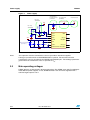
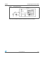
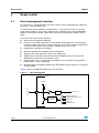
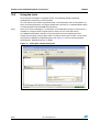
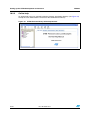
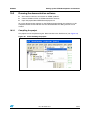
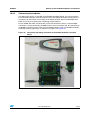
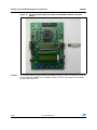
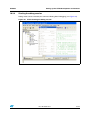
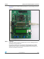
AN3029
Application note
Getting started with STM8L
Introduction
This application note complements the information in the STM8L datasheets by describing
the minimum hardware and software environment required to build an application around an
STM8L 8-bit microcontroller device.
A brief description of the principal hardware components is given. The power supply,
analog-to-digital converter (ADC), clock management, and reset control are described in
some detail. In addition, some hardware recommendations are given. This application note
also contains detailed reference design schematics with descriptions of the main
components. The STM8L uses the same toolchain The STM8 development tools and
software toolchain are common to STM8L, STM8S and STM8A and are presented in
Section 8, and 9. Section 10 describes how to set up the STM8 development environment.
Finally, Section 11 provides a list of relevant documentation and online support resources.
September 2009
Doc ID 16139 Rev 1
1/42
www.st.com
Contents
AN3029
Contents
1
Hardware requirements summary . . . . . . . . . . . . . . . . . . . . . . . . . . . . . . 7
2
Power supply . . . . . . . . . . . . . . . . . . . . . . . . . . . . . . . . . . . . . . . . . . . . . . . 7
3
4
5
2.1
Power supply overview . . . . . . . . . . . . . . . . . . . . . . . . . . . . . . . . . . . . . . . . 7
2.2
Main operating voltages . . . . . . . . . . . . . . . . . . . . . . . . . . . . . . . . . . . . . . . 8
2.3
Power-on/power-down reset (POR/PDR) . . . . . . . . . . . . . . . . . . . . . . . . . . 9
Analog-to-digital converter (ADC) . . . . . . . . . . . . . . . . . . . . . . . . . . . . . 10
3.1
Analog power . . . . . . . . . . . . . . . . . . . . . . . . . . . . . . . . . . . . . . . . . . . . . . 10
3.2
Analog input . . . . . . . . . . . . . . . . . . . . . . . . . . . . . . . . . . . . . . . . . . . . . . . 10
Clock management . . . . . . . . . . . . . . . . . . . . . . . . . . . . . . . . . . . . . . . . . 12
4.1
Clock management overview . . . . . . . . . . . . . . . . . . . . . . . . . . . . . . . . . . 12
4.2
Internal clocks . . . . . . . . . . . . . . . . . . . . . . . . . . . . . . . . . . . . . . . . . . . . . 12
4.3
External clock . . . . . . . . . . . . . . . . . . . . . . . . . . . . . . . . . . . . . . . . . . . . . . 12
5.2
2/42
HSE clock . . . . . . . . . . . . . . . . . . . . . . . . . . . . . . . . . . . . . . . . . . . . . . . 12
4.3.2
LSE clock . . . . . . . . . . . . . . . . . . . . . . . . . . . . . . . . . . . . . . . . . . . . . . . . 14
4.3.3
External source (LSE bypass) . . . . . . . . . . . . . . . . . . . . . . . . . . . . . . . . 15
4.3.4
External crystal/ceramic resonator (LSE crystal) . . . . . . . . . . . . . . . . . . 15
Reset control . . . . . . . . . . . . . . . . . . . . . . . . . . . . . . . . . . . . . . . . . . . . . . 16
5.1
6
4.3.1
Reset management overview . . . . . . . . . . . . . . . . . . . . . . . . . . . . . . . . . . 16
5.1.1
Output characteristics . . . . . . . . . . . . . . . . . . . . . . . . . . . . . . . . . . . . . . 17
5.1.2
Input characteristics . . . . . . . . . . . . . . . . . . . . . . . . . . . . . . . . . . . . . . . . 17
Hardware reset implementation . . . . . . . . . . . . . . . . . . . . . . . . . . . . . . . . 17
Recommendations . . . . . . . . . . . . . . . . . . . . . . . . . . . . . . . . . . . . . . . . . 18
6.1
Printed circuit board . . . . . . . . . . . . . . . . . . . . . . . . . . . . . . . . . . . . . . . . . 18
6.2
Component position . . . . . . . . . . . . . . . . . . . . . . . . . . . . . . . . . . . . . . . . . 18
6.3
Ground and power supply (VSS, VDD) . . . . . . . . . . . . . . . . . . . . . . . . . . . 18
6.4
Decoupling . . . . . . . . . . . . . . . . . . . . . . . . . . . . . . . . . . . . . . . . . . . . . . . . 18
6.5
Other signals . . . . . . . . . . . . . . . . . . . . . . . . . . . . . . . . . . . . . . . . . . . . . . 19
6.6
Unused I/Os and features . . . . . . . . . . . . . . . . . . . . . . . . . . . . . . . . . . . . 19
Doc ID 16139 Rev 1
AN3029
7
8
Contents
6.7
User options . . . . . . . . . . . . . . . . . . . . . . . . . . . . . . . . . . . . . . . . . . . . . . . 19
6.8
Bootloader . . . . . . . . . . . . . . . . . . . . . . . . . . . . . . . . . . . . . . . . . . . . . . . . 19
Reference design . . . . . . . . . . . . . . . . . . . . . . . . . . . . . . . . . . . . . . . . . . 20
7.1
Component references . . . . . . . . . . . . . . . . . . . . . . . . . . . . . . . . . . . . . . . 20
7.2
Schematics . . . . . . . . . . . . . . . . . . . . . . . . . . . . . . . . . . . . . . . . . . . . . . . . 21
STM8 development tools . . . . . . . . . . . . . . . . . . . . . . . . . . . . . . . . . . . . 22
8.1
8.2
8.3
9
10
Single wire interface module (SWIM) . . . . . . . . . . . . . . . . . . . . . . . . . . . . 22
8.1.1
SWIM overview . . . . . . . . . . . . . . . . . . . . . . . . . . . . . . . . . . . . . . . . . . . 22
8.1.2
SWIM connector pins . . . . . . . . . . . . . . . . . . . . . . . . . . . . . . . . . . . . . . . 23
8.1.3
Hardware connection . . . . . . . . . . . . . . . . . . . . . . . . . . . . . . . . . . . . . . . 23
STice emulator . . . . . . . . . . . . . . . . . . . . . . . . . . . . . . . . . . . . . . . . . . . . . 24
8.2.1
STice overview . . . . . . . . . . . . . . . . . . . . . . . . . . . . . . . . . . . . . . . . . . . . 24
8.2.2
STice in emulation configuration . . . . . . . . . . . . . . . . . . . . . . . . . . . . . . 25
8.2.3
In-circuit programming and debugging . . . . . . . . . . . . . . . . . . . . . . . . . 26
RLink and STLink . . . . . . . . . . . . . . . . . . . . . . . . . . . . . . . . . . . . . . . . . . . 26
STM8 software toolchain . . . . . . . . . . . . . . . . . . . . . . . . . . . . . . . . . . . . 27
9.1
Integrated development environment . . . . . . . . . . . . . . . . . . . . . . . . . . . . 28
9.2
Compiler . . . . . . . . . . . . . . . . . . . . . . . . . . . . . . . . . . . . . . . . . . . . . . . . . . 28
9.3
Firmware library . . . . . . . . . . . . . . . . . . . . . . . . . . . . . . . . . . . . . . . . . . . . 28
Setting up the STM8 development environment . . . . . . . . . . . . . . . . . 29
10.1
Installing the tools . . . . . . . . . . . . . . . . . . . . . . . . . . . . . . . . . . . . . . . . . . . 29
10.2
Using the tools . . . . . . . . . . . . . . . . . . . . . . . . . . . . . . . . . . . . . . . . . . . . . 30
10.3
10.2.1
Project editing . . . . . . . . . . . . . . . . . . . . . . . . . . . . . . . . . . . . . . . . . . . . 31
10.2.2
Online help . . . . . . . . . . . . . . . . . . . . . . . . . . . . . . . . . . . . . . . . . . . . . . . 32
Running the demonstration software . . . . . . . . . . . . . . . . . . . . . . . . . . . . 33
10.3.1
Compiling the project . . . . . . . . . . . . . . . . . . . . . . . . . . . . . . . . . . . . . . . 33
10.3.2
Selecting the correct debug instrument . . . . . . . . . . . . . . . . . . . . . . . . . 34
10.3.3
Connecting the hardware . . . . . . . . . . . . . . . . . . . . . . . . . . . . . . . . . . . . 35
10.3.4
Starting the debug session . . . . . . . . . . . . . . . . . . . . . . . . . . . . . . . . . . 37
10.3.5
Running the software . . . . . . . . . . . . . . . . . . . . . . . . . . . . . . . . . . . . . . . 38
10.3.6
Follow up . . . . . . . . . . . . . . . . . . . . . . . . . . . . . . . . . . . . . . . . . . . . . . . . 39
Doc ID 16139 Rev 1
3/42
Contents
AN3029
11
Documentation and online support . . . . . . . . . . . . . . . . . . . . . . . . . . . . 40
12
Revision history . . . . . . . . . . . . . . . . . . . . . . . . . . . . . . . . . . . . . . . . . . . 41
4/42
Doc ID 16139 Rev 1
AN3029
List of tables
List of tables
Table 1.
Table 2.
Table 3.
Component list . . . . . . . . . . . . . . . . . . . . . . . . . . . . . . . . . . . . . . . . . . . . . . . . . . . . . . . . . . 20
SWIM connector pins . . . . . . . . . . . . . . . . . . . . . . . . . . . . . . . . . . . . . . . . . . . . . . . . . . . . . 23
Document revision history . . . . . . . . . . . . . . . . . . . . . . . . . . . . . . . . . . . . . . . . . . . . . . . . . 41
Doc ID 16139 Rev 1
5/42
List of figures
AN3029
List of figures
Figure 1.
Figure 2.
Figure 3.
Figure 4.
Figure 5.
Figure 6.
Figure 7.
Figure 8.
Figure 9.
Figure 10.
Figure 11.
Figure 12.
Figure 13.
Figure 14.
Figure 15.
Figure 16.
Figure 17.
Figure 18.
Figure 19.
Figure 20.
Figure 21.
Figure 22.
Figure 23.
Figure 24.
Figure 25.
Figure 26.
6/42
Power supply . . . . . . . . . . . . . . . . . . . . . . . . . . . . . . . . . . . . . . . . . . . . . . . . . . . . . . . . . . . . 8
Typical layout of VDD/VSS pair . . . . . . . . . . . . . . . . . . . . . . . . . . . . . . . . . . . . . . . . . . . . . . . 9
Analog input interface . . . . . . . . . . . . . . . . . . . . . . . . . . . . . . . . . . . . . . . . . . . . . . . . . . . . . 11
HSE clock sources . . . . . . . . . . . . . . . . . . . . . . . . . . . . . . . . . . . . . . . . . . . . . . . . . . . . . . . 13
External clock . . . . . . . . . . . . . . . . . . . . . . . . . . . . . . . . . . . . . . . . . . . . . . . . . . . . . . . . . . . 14
Crystal/ceramic resonators . . . . . . . . . . . . . . . . . . . . . . . . . . . . . . . . . . . . . . . . . . . . . . . . . 14
Reset management . . . . . . . . . . . . . . . . . . . . . . . . . . . . . . . . . . . . . . . . . . . . . . . . . . . . . . 16
Output characteristics . . . . . . . . . . . . . . . . . . . . . . . . . . . . . . . . . . . . . . . . . . . . . . . . . . . . . 17
Input characteristics . . . . . . . . . . . . . . . . . . . . . . . . . . . . . . . . . . . . . . . . . . . . . . . . . . . . . . 17
Reference design . . . . . . . . . . . . . . . . . . . . . . . . . . . . . . . . . . . . . . . . . . . . . . . . . . . . . . . . 21
Debug system block diagram . . . . . . . . . . . . . . . . . . . . . . . . . . . . . . . . . . . . . . . . . . . . . . . 22
Hardware connection . . . . . . . . . . . . . . . . . . . . . . . . . . . . . . . . . . . . . . . . . . . . . . . . . . . . . 23
Connection description . . . . . . . . . . . . . . . . . . . . . . . . . . . . . . . . . . . . . . . . . . . . . . . . . . . . 24
STice in emulation configuration . . . . . . . . . . . . . . . . . . . . . . . . . . . . . . . . . . . . . . . . . . . . 25
In-circuit programming and debugging . . . . . . . . . . . . . . . . . . . . . . . . . . . . . . . . . . . . . . . . 26
STM8 software toolchain . . . . . . . . . . . . . . . . . . . . . . . . . . . . . . . . . . . . . . . . . . . . . . . . . . 27
STVD open example workspace . . . . . . . . . . . . . . . . . . . . . . . . . . . . . . . . . . . . . . . . . . . . 30
STVD MCU edit mode . . . . . . . . . . . . . . . . . . . . . . . . . . . . . . . . . . . . . . . . . . . . . . . . . . . . 31
STM8 firmware library online help manual . . . . . . . . . . . . . . . . . . . . . . . . . . . . . . . . . . . . . 32
STVD: Building the project . . . . . . . . . . . . . . . . . . . . . . . . . . . . . . . . . . . . . . . . . . . . . . . . . 33
STVD: Selecting the debug instrument. . . . . . . . . . . . . . . . . . . . . . . . . . . . . . . . . . . . . . . . 34
Connecting the debug instrument to the STM8L101-EVAL evaluation board . . . . . . . . . . 35
Connecting the debug instrument to the STM8L15x-EVAL evaluation board . . . . . . . . . . 36
STVD: Starting the debug session . . . . . . . . . . . . . . . . . . . . . . . . . . . . . . . . . . . . . . . . . . . 37
STVD: Run the software . . . . . . . . . . . . . . . . . . . . . . . . . . . . . . . . . . . . . . . . . . . . . . . . . . . 38
STM8 evaluation board. . . . . . . . . . . . . . . . . . . . . . . . . . . . . . . . . . . . . . . . . . . . . . . . . . . . 39
Doc ID 16139 Rev 1
AN3029
1
Hardware requirements summary
Hardware requirements summary
To build an application around an STM8L device, the application board should provide the
following features:
●
Power supply (mandatory)
●
Clock management (optional)
●
Reset management (optional)
●
Debugging tool support: Single wire interface module (SWIM) connector (optional)
2
Power supply
2.1
Power supply overview
The STM8L101 can be supplied through a 1.65 V to 3.6 V external source. The STM8L15x
can be supplied through a 1.8 V to 3.6 V external source. However, after startup it can run
on voltages down to 1.65 V.
An on-chip power management system provides the constant digital supply to the core logic,
both in normal and low power modes. This garantees that the logic consumes a constant
current over the voltage range. It is also capable of detecting voltage drops and generate
reset to avoid heratic behaviour.
The STM8L device also provides:
●
One pair of pads, VDD/VSS (1.65 V or 1.8 V to 3.6 V)
The STM8L15x device also provides in the 48-pin package:
●
One pairs of pads dedicated for VDDIO/VSSIO, which are used to power only the I/O’s.
VDDIO and VSSIO must be at the same potential respectively as VDD and VSS.
●
One pair of pads, VDDA/VSSA, dedicated to analog functions. VDDA and VSSA must be at
the same potential respectively as VDD and VSS. Refer to Section 3: Analog-to-digital
converter (ADC) for more details.
The STM8L152 device manages the supply voltage needed by the LCD in three different
ways (see Figure 1):
1.
If the LCD feature is not used, connect the VLCD pin to VDD.
2.
Apply to VLCD the voltage to be applied to the LCD.
3.
Leave the STM8L152 to provide the correct voltage, via its programmable LCD booster,
by connecting the VLCD pin to a 1µF capacitor.
Doc ID 16139 Rev 1
7/42
Power supply
Figure 1.
AN3029
Power supply
Only if internal
booster is used to
power LCD
For noisy
environment
To power LCD
specifi cally
If LCD is unused
2.5V<VLCD<3.6V
VDD
VDD
1uF
100uH
BEAD
For noisy
environment
OR
OR
VSS
100 Ohm
1uF
100nF
NRST
VDDA
100nF
VSS
VRef+
VDD
VSS
3.6 V-1.8 V (1.65 V)
(see note 1)
VLCD
VDDIO
OSC_IN
OSC_OUT
VDD
1uF
100nF
100nF
VSSIO
OSC32_IN
VSS/VSSA/VRef- OSC32_OUT
Biggest package
VSS
1. The device keeps operating as long as the battery voltage is above 1.65 V and no reset is generated.
Note:
The capacitors must be connected as close as possible to the device supplies.
Placing a crystal/resonator on OSCIN/OSCOUT is optional. The resonator must be
connected as close as possible to the OSCIN and OSCOUT pins. The loading capacitance
ground must be connected as close as possible to VSS.
2.2
Main operating voltages
STM8L devices are processed in 0.13 µm technology. The STM8L core and I/O peripherals
need different power supplies. In fact, STM8L devices have an internal regulator with a
nominal target output of 1.8 V.
8/42
Doc ID 16139 Rev 1
AN3029
2.3
Power supply
Power-on/power-down reset (POR/PDR)
The input supply to the main and low power regulators is monitored by a power-on/powerdown reset circuit. The monitoring voltage begins at 0.7 V.
During power-on, the POR/PDR keeps the device under reset until the supply voltages (VDD
and VDDIO) reach their specified working area. This internal reset is maintained during ~1ms
in order to wait for supply stabilization.
At power-on, a defined reset should be maintained below 0.7 V. The upper threshold for a
reset release is defined in the electrical characteristics section of the product datasheets.
A hysteresis is implemented (POR > PDR) to ensure clean detection of voltage rise and fall.
The POR/PDR also generates a reset when the supply voltage drops below the VPOR/PDR
threshold (isolated and repetitive events).
For better power monitoring, the STM8L15x provides a programmable power voltage
detection (PVD) and a brown out reset (BOR) for an earlier detection of voltage drop.
Recommendations
All pins need to be properly connected to the power supplies. These connections, including
pads, tracks and vias should have the lowest possible impedance. This is typically achieved
with thick track widths and preferably dedicated power supply planes in multi-layer printed
circuit boards (PCBs).
In addition, each power supply pair should be decoupled with filtering ceramic capacitors (C)
at 100 nF with one chemical C (1..2 µF) in parallel on the STM8L device. The ceramic
capacitors should be placed as close as possible to the appropriate pins, or below the
appropriate pins, on the opposite side of the PCB. Typical values are 10 nF to 100 nF, but
exact values depend on the application needs. Figure 2 shows the typical layout of such a
VDD/VSS pair.
Figure 2.
Typical layout of VDD/VSS pair
Via to VDD
Via to VSS
Cap.
VDD
VSS
STM8
Doc ID 16139 Rev 1
9/42
Analog-to-digital converter (ADC)
3
AN3029
Analog-to-digital converter (ADC)
This section is unique for the STM8L15x.
3.1
Analog power
For 48-pin packages, the ADC unit has an independent, analog supply voltage, isolated on
input pin VDDA, which allows the ADC to accept a very clean voltage source. This analog
voltage, VDDA, should be identical to the digital voltage supply on pin VDD. To filter some
noise, a ferrite bead can be added between VDD and VDDA. This ferrite bead should be
choosen according to the frequencies to be filtered.
The 48-pin package also provides a separate external analog reference voltage input for the
ADC unit on the VREF+ pin. This gives better accuracy on low voltage input as follows:
3.2
●
VREF+ (input, analog reference positive): The higher/positive reference voltage for the
ADC should be below or equal to VDDA. When VDDA is below 2.4 V, VREF+ must be
equal to VDDA. This input is bonded to VDDA in devices that have no external VREF+ pin
(packages with 32 pins or less).
●
VREF- (input, analog reference negative): The lower/negative reference voltage is
internally bonded to VSSA .
Analog input
STM8L15x devices have up to 28 analog input channels (including four fast channels), each
multiplexed with an I/O, which are converted by the ADC one at a time.
The analog input interface of the ADC is shown in Figure 3. The RADC, CADC, and IL real
values are given in the chip datasheet. The external input impedance (RAIN) max value, in
order to achieve an error below 1/4 of LSB can be calculated with the formula:
Equation 1
Nsc
R ain < ------------------------------------------------------------------------------------------------------- – R ADC
2
N+2
( f CPU ⁄ prescal ) × C TOTAL × In ( 2
)
Where:
fCPU is the CPU frequency.
Prescal is a programmable ADC clock prescaler with a value of 1 or 2. Usually fCPU/prescal
is between 0.320 MHz and 16 MHz.
Nsc is the programmable number of sampling cycles. Usually the minimum number of
cycles is four and the maximum is 384.
CTOTAL is the approximate sum of Cparasitic and CADC.
N is the resolution which is programable between 6 and 12, but is usually 12.
RADC is the sampling switch resistance which is usually around 1kΩ..
Please refer to Figure 3.
10/42
Doc ID 16139 Rev 1
AN3029
Analog-to-digital converter (ADC)
Figure 3.
Analog input interface
STM8L15x
Please refer to the STM8L15x datasheet and reference manual for more details.
Doc ID 16139 Rev 1
11/42
Clock management
4
AN3029
Clock management
The STM8L101 has no external clock so no precautionary measures are needed. The
following paragraph deals with STM8L15x chips only.
4.1
Clock management overview
STM8L15x devices offer a flexible way of selecting the core and peripheral clocks (ADC,
memory, and digital peripherals). The devices have internal and external clock source
inputs, both of which have a high speed and a low speed version. Any of those four clocks
can be use for the CPU and most of the peripherals through a programable prescaler. An I/O
can be programmed as output clock (CCO) to reflect one of the four clocks (with or without
prescaling).
The signal which leaves the I/O represents an output clock (CCO) divided by a division
factor.
4.2
Internal clocks
STM8L devices have two kinds of internal clock: A high speed internal clock (HSI) running at
16 MHz and a low speed internal clock (LSI) running at 38 kHz.
After reset, the CPU starts with the internal RC (HSI clock signal) divided by 8, i.e. 2 MHz.
4.3
External clock
STM8L devices have two kinds of external clock: A high speed external clock (HSE) running
at up to 16 MHz and a low speed external clock (LSE) running at 32.768 kHz.
4.3.1
HSE clock
STM8L15x devices can connect to an external crystal or an external oscillator.
Note:
When no external clock is used, OSCIN and OSCOUT can be used as general purpose
I/Os.
Figure 4 describes the external clock connections.
External clock
Caution:
12/42
●
Frequency: 0 kHz … 16 MHz
●
Input hysteresis: 100 mV
Without prescaler, a duty cycle of 45/55 % maximum must be respected at high speed
Doc ID 16139 Rev 1
AN3029
Clock management
Crystal/ceramic resonator
●
Frequency range: 1 to 16 MHz
●
Stabilisation time: Programable from 1 to 4096 cycles
●
Oscillation mode: Preferred fundamental
●
Output duty cycle: Max 55/45%
●
I/O’s: Standard I/O pins multiplexed with OSCIN and OSCOUT
●
Cload: 10 to 20 pF
●
Drive level maximum: at least 100 µW
Figure 4.
HSE clock sources
Hardware configuration
External clock
STM8
OSCIN
OSCOUT
(I/O available)
Crystal/ceramic resonators(1)
External source
STM8
OSCIN
OSCOUT
Q1
CL1
REXT (1)
CL2
Load capacitors
1. The value of REXT depends on the crystal characteristics. A 0 Ω resistor works well with most oscillators
but, it is not optimal. A typical value is in the range 5 to 6 RS (resonator series resistance). To fine-tune the
REXT value, refer to AN2867 (Oscillator design guide for ST microcontrollers).
The values of the load capacitors CL1 and CL2 are heavily dependent on the crystal type and
frequency. Refer to the datasheet of the crystal manufacturer to select the capacitances. For
best oscillation stability, CL1 and CL2 normally have the same value. Typical values are in the
range from below 20 pF up to 40 pF (cload: 10 to 20 pF). The parasitic capacitance of the
board layout also needs to be considered and typically adds a few pF to the component
values.
A clock security system prevents any CPU fatal error from a HSE failure, as it safely
switches to HSI.
Doc ID 16139 Rev 1
13/42
Clock management
AN3029
Recommendations
In the PCB layout all connections should be as short as possible. Any additional signals,
especially those that could interfere with the oscillator, should be locally separated from the
PCB area around the oscillation circuit using suitable shielding.
4.3.2
LSE clock
The low-speed external clock signal (LSE) can be generated from two possible clock
sources:
●
LSE external crystal/ceramic resonator (see Figure 5)
●
LSE user external clock (see Figure 6)
Figure 5.
External clock
Microcontroller
OSC32_IN OSC32_OUT
(Hi-Z)
External source
ai15765
1. OSC32_IN and OSC32_OUT pins can be used also as GPIO but, it is recommended not to use them as
both RTC and GPIO pins in the same application.
Figure 6.
Crystal/ceramic resonators
Microcontroller
OSC32_IN
OSC32_OUT
REXT(3)
CL1
CL2
ai15764
1. To avoid exceeding the maximum value of CL1 and CL2 (15 pF), it is strongly recommended to use a
resonator with a load capacitance CL = 7 pF. To fine-tune the choice, refer to the gmcrit calculation in
AN2867 (Oscillator design guide for ST microcontrollers).
2. OSC32_IN and OSC32_OUT pins can be used also as GPIO, but it is recommended not to use them as
both RTC and GPIO pins in the same application.
3. The value of REXT depends on the crystal characteristics. A 0 Ω resistor works with most oscillators. A
typical value is in the range 5 to 6 RS. To fine-tune the REXT value refer to AN2867 (Oscillator design guide
for ST microcontrollers).
14/42
Doc ID 16139 Rev 1
AN3029
4.3.3
Clock management
External source (LSE bypass)
In this mode, an external clock source must be provided. It must have a frequency of
32.768 kHz. The external clock signal (square, sine or triangle) with a duty cycle of about
50% has to drive the OSC32_IN pin while the OSC32_OUT pin must be left high impedance
(see Figure 5 and Figure 6).
4.3.4
External crystal/ceramic resonator (LSE crystal)
The LSE crystal is a 32.768 kHz low-speed external crystal or ceramic resonator. It has the
advantage of providing a low-power, but highly accurate clock source to the real-time clock
peripheral (RTC) for clock/calendar or other timing functions.
The resonator and the load capacitors have to be connected as close as possible to the
oscillator pins in order to minimize output distortion and start-up stabilization time. The load
capacitance values must be adjusted according to the selected oscillator.
Doc ID 16139 Rev 1
15/42
Reset control
AN3029
5
Reset control
5.1
Reset management overview
The reset pin is a 3.3 V bidirectional I/O. After startup it can be programmed by software to
be used as a general purpose I/O.
Its output buffer driving capability is fixed to IolMIN = 2 mA @ 0.45 V in the 1.8 V to 3.6 V
range which includes a ~45 k pull-up. Output buffer is reduced to the n-channel MOSFET
(NMOS). The receiver includes a glitch filter, whereas the output buffer includes a 20 µs
delay.
There are many reset sources, including:
●
External reset through the NRST pin
●
Power-on reset (POR) and brown-out reset (BOR): During power-on, the POR keeps
the device under reset until the supply voltage (VDD and VDDIO) reach the voltage level
at which level the BOR starts to function. STM8L101 has only a POR.
●
Independent watchdog reset (IWDG)
●
Window watchdog reset (WWDG), only for STM8L15x
●
Software reset: The application software can trigger reset
●
SWIM reset: An external device connected to the SWIM interface can request the
SWIM block to generate a microcontroller reset.
●
Illegal opcode reset: If a code to be executed does not correspond to any opcode or
prebyte value, a reset is generated.
●
Electromagnetic susceptibility (EMS) reset: Generated if critical registers are corrupted
or badly loaded.
Figure 7 shows a simplified functional I/O reset schematic.
Figure 7.
Reset management
STM8
VDD_IO
External reset
RPU
Filter
NRST
System reset
Illegal op code reset
Pulse generator
(min 20 µs
Delay
16/42
Doc ID 16139 Rev 1
IWDG/WWDG/software reset
SWIM reset
EMS reset
POR/BOR reset
AN3029
5.1.1
Reset control
Output characteristics
●
A valid pulse on the pin is guaranteed with a ≥ 20 ns pulse duration on the internal
output buffer.
●
After a valid pulse is recognized, a pulse on the pin of at least 20 µs is guaranteed
starting from the falling edge of A.
Figure 8.
Output characteristics
≥ 20 n
A
20 µs pulse stretch min
Pad
Reset requested
5.1.2
Input characteristics
●
All pulses with a duration less than 50 ns are filtered
●
All train/burst spikes with a ratio of 1/10 must be filtered. This means that a negative
spike of up to 50 ns is always filtered, when a 5 ns interval between spikes occurs (ratio
1/10).
●
All pulses with duration more than 300 ns are recognized as valid pulses
Figure 9.
Input characteristics
>5 ns
>5 ns
300 ns
<50 ns
<50 ns
Negative train of glitch filtered
5.2
Pad
<50 ns
Valid Reset requested
System reset
Hardware reset implementation
In most cases, the STM8L does not require an external reset circuit to power-up correctly.
The STM8L101 reset state is released 1 ms after the POR value (1.35 V to 1.65 V) is
reached. At this time, VDD should be in the 1.65 V to 3.6 V range.
The STM8L15x reset state is released 1 ms after the BOR minimum value (~1.75 V) is
reached.
Doc ID 16139 Rev 1
17/42
Recommendations
AN3029
6
Recommendations
6.1
Printed circuit board
For technical reasons, it is best to use a multi-layer PCB with a separate layer dedicated to
the VSS and another layer to the VDD supply. This results in a good decoupling, as well as a
good shielding effect. For many applications, economical requirements prohibit the use of
this type of board. In this case, the most important feature is to ensure a good structure for
the VSS and power supply.
6.2
Component position
A preliminary layout of the PCB must separate the different circuits according to their
electromagnetic interference (EMI) contribution. This reduces cross-coupling on the PCB,
for instance, noisy, high-current circuits, low voltage circuits, and digital components.
6.3
Ground and power supply (VSS, VDD)
The VSS should be distributed individually to every block (noisy, low level sensitive, and
digital) with a single point for gathering all ground returns. Loops must be avoided or have a
minimum surface. The power supply should be implemented close to the ground line to
minimize the surface of the supply loop. This is due to the fact that the supply loop acts as
an antenna, and is therefore the main emitter and receiver of EMI. All component-free
surfaces of the PCB must be filled with additional grounding to create a kind of shield
(especially when using single-layer PCBs).
6.4
Decoupling
The standard decoupler for the external power is a 100 µF pool capacitor. Supplementary
100 nF capacitors must be placed as close as possible to the VSS/VDD pins of the
microcontroller to reduce the area of the current loop.
As a general rule, decoupling all sensitive or noisy signals improves electromagnetic compatibility (EMC) performances.
There are two types of decouplers:
18/42
●
Capacitors close to components. Inductive characteristics, which apply to all capacitors
beyond a certain frequency, must be taken into account. If possible, parallel capacitors
with decreasing values (0.1, 0.01,... µF) should be used.
●
Inductors. Although often ignored, ferrite beads, for example, are excellent inductors
due to their good dissipation of EMI energy and there is no loss of DC voltage (which is
not the case when simple resistors are used).
Doc ID 16139 Rev 1
AN3029
6.5
Recommendations
Other signals
When designing an application, the following areas should be closely studied to improve
EMC performances:
●
Noisy signals (clock)
●
Sensitive signals (high impedance)
Signals for which a temporary disturbance permanently affects operation of the
application, for example, interrupts and handshaking strobe signals (but not LED
commands).
●
A surrounding VSS trace for such signals increases EMC performances, as does a shorter
length or absence of noisy and sensitive traces (crosstalk effect).
For digital signals, the best possible electrical margin must be reached for the two logical
states. Slow Schmitt triggers are recommended for eliminating parasitic states.
6.6
Unused I/Os and features
Microcontrollers are designed for a variety of applications, where often a particular
application does not use 100 % of the microcontroller resources.
To avoid unnecessary power consumption (especially important for battery powered
applications) and also to improve EMC performance, unused clocks, counters, or I/Os,
should not be left free, I/Os should be forced externally (pull-up or pull-down to the unused
I/O pins), and unused functions should be ‘frozen’ or disabled.
Alternatively, unused I/Os can be programmed as push-pull ‘low’ to keep them at a defined
level without using external components. However in this case, the I/O is not driven during
the power up phase, until the I/O is configured. This can add a little extra power
consumption, and may be undesirable in very power sensitive applications.
6.7
User options
STM8L devices have user option features that can be used for remapping or
enabling/disabling an automatic reset or low speed watchdog. For more details, please refer
to the product datasheets.
6.8
Bootloader
STM8L15x devices have a bootloader embedded in a ROM memory. Through this firmware
the device memory can be re-programmed via the USART communication interface.
Doc ID 16139 Rev 1
19/42
Reference design
AN3029
7
Reference design
7.1
Component references
Table 1.
ID
Component list
Component name
Reference
Quantity
Comments
1
Microcontroller
STM8L
1
Refer to the ‘pinouts and pin description’
and ‘package characteristics’ sections of
the STM8L datasheets, to choose the right
package
2
Battery
1.65 V to 3.6 V
1
Min 1.8 V for STM8L15x
3
Capacitor
1 µF
n
Decoupling capacitor
4
Capacitor
100 nF
n
Ceramic capacitor (decoupling capacitor)
Components below are optional
6
Crystal
1 to 16 MHz
1
7
Capacitor
20 to 40 pF
2
Crystal
32 kHz
1
Capacitor
5 to 20 pF
2
8
Ferrite bead
9
20/42
SWIM connector
Used for crystal
Used for crystal
Depends on noise to be filtered
4 pins
1
Doc ID 16139 Rev 1
AN3029
Reference design
7.2
Schematics
Figure 10. Reference design
Only if internal
booster is used to
power LCD
For noisy
environment
To power LCD
specifi cally
If LCD is unused
2.5V<VLCD<3.6V
VDD
VDD
1uF
100uH
BEAD
For noisy
environment
OR
OR
Only if accurate High Speed
Oscillator is needed
VSS
100 Ohm
1uF
100nF
NRST
20pF
VDDA
100nF
VSS
VRef+
VDD
VSS
VDDIO
1-16MHz
OSC_IN
OSC_OUT
0 Ohm
VDD
100nF
VSSIO
20pF
OSC32_IN
1
100nF
2
VSS/VSSA/VRef- OSC32_OUT
6.8pF
32.768 kHz
Biggest package
VSS
4
1uF
3
3.6V-1.8V
(1.65V)*
VLCD
0 Ohm
6.8pF
Only if Accurate oLw Speed
Oscillator si needed
Doc ID 16139 Rev 1
21/42
STM8 development tools
8
AN3029
STM8 development tools
Typically, the following tools are needed to get started:
●
STVD for integrated development environment
●
STM8 C compiler (from Cosmic or Raisonance)
●
ST toolset and STM8 firmware library from STMicroelectronics
(STM8L10x_StdPeriph_Lib for STM8L101 or STM8L15x_StdPeriph_Lib for
STM8L15x).
●
STM8 evaluation board from STMicroelectronics (STM8L101-EVAL for STM8L101 and
STM8L1526-EVAL for STM8L15x).
●
If you use STM8L101-EVAL, you also need the HW debug interface "Rlink" from
Raisonance. The debug interface ST-LINK is included in STM8L1526-EVAL.
8.1
Single wire interface module (SWIM)
8.1.1
SWIM overview
In-circuit debugging mode or in-circuit programming mode are managed through a single
wire hardware interface based on an open-drain line, featuring ultra fast memory
programming. Coupled with an in-circuit debugging module, the SWIM also offers a nonintrusive read/write to RAM and peripherals. This makes the in-circuit debugger extremely
powerful and close in performance to a full-featured emulator.
The SWIM pin can be used as a standard I/O (with 8 mA capability) which has some
restrictions if the user wants to use it for debugging. The most secure way to use it is to
provide a strap option on the PCB. Please refer to the STM8 SWIM communication protocol
and debug module user manual (UM0470) for more SWIM protocol details.
Figure 11. Debug system block diagram
100 kHz Osc
Peripheral
DBG
SWIM entry
Comm CMD
layer decode
DM
STM8
core
RAM
NVM
Internal RC
22/42
Doc ID 16139 Rev 1
AN3029
8.1.2
STM8 development tools
SWIM connector pins
The SWIM connector pins consist of four pins as described in Table 2.
Table 2.
8.1.3
SWIM connector pins
Pin number
Pin name
Pin 1
VDD
Pin 2
SWIM pin
Pin 3
VSS
Pin 4
Reset
Hardware connection
Figure 12. Hardware connection
AD/ICC SWIM adapter
Application board
SWIM connector
VDD
1
1
2
3
2
3
4
4
VDD
STM8
SWIM cable
Caution:
It is recommended to place the SWIM header as close as possible to the STM8L device, as
this minimizes any possible signal degradation caused by long PCB tracks.
Doc ID 16139 Rev 1
23/42
STM8 development tools
8.2
STice emulator
8.2.1
STice overview
AN3029
The STice is a modular, high-end emulator system which connects to the PC via a USB
interface, and to the application board in place of the target microcontroller.
It is supported by the free STM8 toolset: IDE ST visual develop (STVD) programmer, ST
visual programmer (STVP) and STM8 assembler. Please refer to the STice emulator for
STM8 for more details.
STice has two distinct modes of operation which are described further in this section:
●
Emulation mode
●
In-circuit mode
It can also be used instead of RLink for SWIM connection.
Figure 13. Connection description
Emulation system
Connection flex
Connection adapter
Adapter socket
Emulation system: STice
●
Emulator box
●
Cables for USB, power supply, trigger, and analyzer input
Connection flex
●
60-pin or 120-pin cable for connection to the application board
Connection adapter
●
Links the connection flex to the footprint of the STM8L microcontroller
Adapter socket
●
24/42
Package-specific socket for connection adapter and STM8L microcontroller
Doc ID 16139 Rev 1
AN3029
8.2.2
STM8 development tools
STice in emulation configuration
In emulation configuration, the STice is connected to the PC via a USB interface and to the
application board in place of the target microcontroller being used.
●
Connection flex: Flexible cable (60-pin or 120-pin depending on the target
microcontroller) that relays signals from the STice to the application board.
●
Connection adapter: Links the connection flex to the footprint of the target
microcontroller on the users application board.
●
Adapter socket: Socket that solders to the application board in place of the
microcontroller and receives the connection adapter.
The above accessories are not included with the STice system. To determine exactly what
is required for any supported microcontroller, refer to the online product selector on
www.st.com.
Figure 14. STice in emulation configuration
Doc ID 16139 Rev 1
25/42
STM8 development tools
8.2.3
AN3029
In-circuit programming and debugging
In the in-circuit debugging/programming configuration, STice allows the application to be
programmed in the microcontroller and for the application to be debugged while it runs on
the microcontroller on the application board. STice supports the SWIM protocol, making it
possible to in-circuit program and debug the microcontroller using only one general purpose
I/O.
In both the emulation and the in-circuit programming/debugging configuration, STice is
driven by the ST visual develop (STVD) or ST visual programmer (STVP) integrated
development environment running on the host PC. This provides total control of advanced
application building, debugging and programming features from a single easy-to-use
interface.
Figure 15. In-circuit programming and debugging
8.3
RLink and STLink
RLink and STLink are debug tools that allow the STM8L evaluation board or any user
application board with the SWIM interface to be connected to a host PC via USB for
debugging and programming. See Section 10.3.3: Connecting the hardware on page 35.
26/42
Doc ID 16139 Rev 1
AN3029
9
STM8 software toolchain
STM8 software toolchain
To write, compile and run the first software on an STM8L device, the following components
of the software toolchain are required (see Figure 16):
●
Integrated development environment
●
Compiler
●
Firmware library (optional, used to ease the start-up)
Figure 16. STM8 software toolchain
Doc ID 16139 Rev 1
27/42
STM8 software toolchain
9.1
AN3029
Integrated development environment
The integrated development environment ST visual develop (STVD) provides an easy-touse, efficient environment for start-to-finish control of application development, from building
and debugging the application code to programming the microcontroller. STVD is delivered
as part of the free ST toolset, which also includes the ST visual programmer (STVP)
programming interface and the ST assembler linker.
To build applications, STVD provides seamless integration of C and assembly tool chains for
ST including the Cosmic and Raisonance C compilers and the ST assembler linker. When
debugging, STVD provides an integrated simulator (software) and supports a complete
range of hardware tools including the low-cost RLink in-circuit debugger/programmer and
the high-end STice emulator.
To program applications to an STM8L, the STVD also provides an interface for reading from
the microcontroller memories, writing to them and verifying them. This interface is based on
the ST visual programmer (STVP), and supports all the target devices and programming
tools supported by STVP.
The free ST toolset for STM8 is available from STMicroelectronics homepage (see
www.st.com).
9.2
Compiler
STM8L devices can be programmed by a free assembler toolchain which is included in the
ST toolset.
As the core is designed for optimized high-level-language support, use of a C compiler is
recommended!
C compilers for STM8 are offered by the third party companies Cosmic and Raisonance.
A free version of the C compiler with up to 16 Kbytes of generated code is available at:
www.cosmic-software.com and www.raisonance.com.
9.3
Firmware library
The STM8 firmware library is a complete set of source code examples for each STM8
peripheral. It is written in strict ANSI-C and it is fully MISRA C 2004 compliant.
All examples are delivered with three workspace and project definition files,one for STVD
and Cosmic C compiler, one for STVD and raisonance Compiler, and one for Raisonance
integrated debugging environment and compiler. This enables the user to load and compile
them easily into their preferred development environment.
The examples run on the STMicroelectronics STM8L evaluation board and can be tailored
easily to other types of hardware.
For additional information and download of the STM8L firmware library connect to
www.st.com/mcu.
28/42
Doc ID 16139 Rev 1
AN3029
10
Setting up the STM8 development environment
Setting up the STM8 development environment
The STM8 development environment setup looks different depending on the supplier of the
software (SW) and hardware (HW) tools.
Typical setups are described below for the following SW and HW tools:
10.1
●
STM8 C compiler from Cosmic
●
ST toolset and STM8 firmware library from STMicroelectronics
(STM8L10x_StdPeriph_Lib for STM8L101 or STM8L15x_StdPeriph_Lib for
STM8L15x).
●
STM8 evaluation board from STMicroelectronics (STM8L101-EVAL for STM8L101 and
STM8L1526-EVAL for STM8L15x).
●
If you use STM8L101-EVAL, you also need the HW debug interface "Rlink" from
Raisonance. The debug interface ST-LINK is included in STM8L1526-EVAL.
Installing the tools
All software tools are delivered with a setup wizard which guides the user through the
installation process. It is recommended to install the tools in the following order:
1.
C compiler
2.
ST toolset
3.
STM8 firmware library
ST-LINK does not need any dedicated software installation in the STM8 development
environment because the necessary drivers are delivered with the ST toolset.
The R-link drivers must be launched separately as follows:
Start/Programs/STtoolset/Setup/Install Rlink driver.
Doc ID 16139 Rev 1
29/42
Setting up the STM8 development environment
10.2
AN3029
Using the tools
Once the tools installation is complete, the ST visual develop (STVD) integrated
development environment can be launched.
The user then has the choice to generate either a new workspace with a new project or to
open an existing workspace. If using the STVD for the first time, it is recommended to open
an existing project from the STM8 firmware library.
Note:
Even if you are not intending to use the library, an existing library project can be used as a
template to configure all the compiler options. Enter your own code after main().
The STM8 firmware library includes several examples for each peripheral plus one
workspace containing a blank project which is ready to receive your C code. It is located in
the firmware subdirectory \Project\Template (see Figure 17). You can choose between
STVD\Cosmic, STVD\Raisonance, or RIDE.
Figure 17. STVD open example workspace
30/42
Doc ID 16139 Rev 1
AN3029
10.2.1
Setting up the STM8 development environment
Project editing
All project source files are visible and can be edited (see Figure 18).
Figure 18. STVD MCU edit mode
Doc ID 16139 Rev 1
31/42
Setting up the STM8 development environment
10.2.2
AN3029
Online help
An online help manual is available inside the firmware installation directory (see Figure 19)
to help the user understand the structure of the STM8 firmware library.
Figure 19. STM8 firmware library online help manual
32/42
Doc ID 16139 Rev 1
AN3029
10.3
Setting up the STM8 development environment
Running the demonstration software
●
Go to www.st.com/mcu and search for STM8L products
●
Choose STM8L1x-EVAL or STM8L1526-EVAL firmware
●
Open the project/demo/STVD/Cosmic/project.stw
To run the demonstration software on the STM8 evaluation board, the project has to be
compiled and the correct HW tool must be selected before the debug session can be
started.
10.3.1
Compiling the project
The project can be compiled using the ‘Build’ function in the ‘Build’ menu (see Figure 20).
Figure 20. STVD: Building the project
Doc ID 16139 Rev 1
33/42
Setting up the STM8 development environment
10.3.2
AN3029
Selecting the correct debug instrument
In the example below, the Rlink tool is used for communicating via the SWIM interface with
the on-board debug module of the STM8.
The Rlink tool can be selected from the ‘Debug Instrument Selection’ list in the ‘Debug
Instrument Settings’ dialog (see Figure 21).
Figure 21. STVD: Selecting the debug instrument
34/42
Doc ID 16139 Rev 1
AN3029
10.3.3
Setting up the STM8 development environment
Connecting the hardware
The debug tool, STLink, is included on the STM8L1526-EVAL board. You can connect the
PC to the USB connector. This connection ensures the debug connection and the power. If
the jumpers on the boards are no longer in the default position, please read STM8L1526EVAL user manual to select power and debug support jumpers.
For the STM8L101-EVAL, the Rlink tool can be connected to the PC by a standard USB
connection. It is also powered by the USB interface. On the controller side, the connection to
the STM8 evaluation board is made using the SWIM interface cable. The STM8L101-EVAL,
evaluation board is powered by an external 5 V supply (see Figure 22).
Figure 22. Connecting the debug instrument to the STM8L101-EVAL evaluation
board
Doc ID 16139 Rev 1
35/42
Setting up the STM8 development environment
AN3029
Figure 23. Connecting the debug instrument to the STM8L15x-EVAL evaluation
board
Caution:
36/42
On the Rlink adapter board for STM8, the “SWIM” jumper must be set. If there is no pull-up
on the application SWIM line, the “ADAPT” jumper is also set. The “PW-5V” and “12MHz”
jumpers must not be set.
Doc ID 16139 Rev 1
AN3029
10.3.4
Setting up the STM8 development environment
Starting the debug session
Debug mode can be entered by the command ‘Debug Start Debugging’ (see Figure 24).
Figure 24. STVD: Starting the debug session
Doc ID 16139 Rev 1
37/42
Setting up the STM8 development environment
10.3.5
AN3029
Running the software
After entering debug mode, the software can be started by the run command in the menu ‘Debug Run’
(see Figure 25).
Figure 25. STVD: Run the software
38/42
Doc ID 16139 Rev 1
AN3029
Setting up the STM8 development environment
The LCD display on the STM8 evaluation board indicates a successful debug session (see
Figure 26).
Figure 26. STM8 evaluation board
10.3.6
Follow up
Step by step, additional peripherals of STM8L devices can be run, following on from the
initial debug session described above.
Many features of STM8L devices are supported by dedicated hardware on the STM8
evaluation board. The necessary software drivers, including STM8L peripheral drivers
(USART, ADC, SPI) and drivers for the EVAL board modules (LCD, serial memory), are
delivered in the STM8L1x firmware library.
Doc ID 16139 Rev 1
39/42
Documentation and online support
11
AN3029
Documentation and online support
Documentation resources related to tool usage includes:
Application
●
STM8L101 and STM8L15x datasheets
●
How to program Flash memory and data EEPROM on STM8L microcontrollers
(PM0054).
●
STM8L101 and STM8L15x reference manuals
●
STM8 CPU programming manual (PM0044)
Tools
●
STM8L101 and STM8L15x firmware library and release note (detailed descriptions of
the library are included as help files).
●
STice advanced emulation system for ST microcontrollers data briefing
●
STice user manual
●
Cosmic or Raisonnance C compiler user manual
●
STM8L101-EVAL or STM8L1526-EVAL evaluation board user manual
●
STM8L1x-EVAL or STM8L1526-EVAL firmware
●
ST visual develop tutorial (included as help files in the ST-toolchain)
●
ST visual develop (STVD) user manual
●
STM8 SWIM communication protocol and debug module user manual (UM0470)
The microcontroller discussion forum on www.st.com can be used by developers to
exchange ideas. It is the best place to find different application ideas. In addition, the
website has a knowledge base of FAQs for microcontrollers, which provide answers to many
queries and solutions to many problems.
40/42
Doc ID 16139 Rev 1
AN3029
12
Revision history
Revision history
Table 3.
Document revision history
Date
Revision
09-Sep-2009
1
Changes
Initial release
Doc ID 16139 Rev 1
41/42
AN3029
Please Read Carefully:
Information in this document is provided solely in connection with ST products. STMicroelectronics NV and its subsidiaries (“ST”) reserve the
right to make changes, corrections, modifications or improvements, to this document, and the products and services described herein at any
time, without notice.
All ST products are sold pursuant to ST’s terms and conditions of sale.
Purchasers are solely responsible for the choice, selection and use of the ST products and services described herein, and ST assumes no
liability whatsoever relating to the choice, selection or use of the ST products and services described herein.
No license, express or implied, by estoppel or otherwise, to any intellectual property rights is granted under this document. If any part of this
document refers to any third party products or services it shall not be deemed a license grant by ST for the use of such third party products
or services, or any intellectual property contained therein or considered as a warranty covering the use in any manner whatsoever of such
third party products or services or any intellectual property contained therein.
UNLESS OTHERWISE SET FORTH IN ST’S TERMS AND CONDITIONS OF SALE ST DISCLAIMS ANY EXPRESS OR IMPLIED
WARRANTY WITH RESPECT TO THE USE AND/OR SALE OF ST PRODUCTS INCLUDING WITHOUT LIMITATION IMPLIED
WARRANTIES OF MERCHANTABILITY, FITNESS FOR A PARTICULAR PURPOSE (AND THEIR EQUIVALENTS UNDER THE LAWS
OF ANY JURISDICTION), OR INFRINGEMENT OF ANY PATENT, COPYRIGHT OR OTHER INTELLECTUAL PROPERTY RIGHT.
UNLESS EXPRESSLY APPROVED IN WRITING BY AN AUTHORIZED ST REPRESENTATIVE, ST PRODUCTS ARE NOT
RECOMMENDED, AUTHORIZED OR WARRANTED FOR USE IN MILITARY, AIR CRAFT, SPACE, LIFE SAVING, OR LIFE SUSTAINING
APPLICATIONS, NOR IN PRODUCTS OR SYSTEMS WHERE FAILURE OR MALFUNCTION MAY RESULT IN PERSONAL INJURY,
DEATH, OR SEVERE PROPERTY OR ENVIRONMENTAL DAMAGE. ST PRODUCTS WHICH ARE NOT SPECIFIED AS "AUTOMOTIVE
GRADE" MAY ONLY BE USED IN AUTOMOTIVE APPLICATIONS AT USER’S OWN RISK.
Resale of ST products with provisions different from the statements and/or technical features set forth in this document shall immediately void
any warranty granted by ST for the ST product or service described herein and shall not create or extend in any manner whatsoever, any
liability of ST.
ST and the ST logo are trademarks or registered trademarks of ST in various countries.
Information in this document supersedes and replaces all information previously supplied.
The ST logo is a registered trademark of STMicroelectronics. All other names are the property of their respective owners.
© 2009 STMicroelectronics - All rights reserved
STMicroelectronics group of companies
Australia - Belgium - Brazil - Canada - China - Czech Republic - Finland - France - Germany - Hong Kong - India - Israel - Italy - Japan Malaysia - Malta - Morocco - Philippines - Singapore - Spain - Sweden - Switzerland - United Kingdom - United States of America
www.st.com
42/42
Doc ID 16139 Rev 1