1
USB 1.1 OHCI Host
Controller Core
User Manual
Core Version 2.2
Manual Version 2.3
October, 00
Proprietary Information
Information specific to the design contained in this document is proprietary to inSilicon
(http://www.in-silicon.com/). It is against the law to copy software on any media except as specifically allowed in the
license or nondisclosure agreement.
Copyright
© Copyright 2000 by inSilicon. All rights reserved. No part of this publication may be reproduced, transmitted,
transcribed, stored in a retrieval system, or translated into any language or computer language, in any form or by any
means, electronic, mechanical, magnetic, optical, chemical, manual, or otherwise, without the prior written permission of
inSilicon.
Disclaimers
INSILICON MAKES NO REPRESENTATIONS OR WARRANTIES WITH RESPECT TO THE DESIGN AND
DOCUMENTATION HEREIN DESCRIBED AND ESPECIALLY DISCLAIMS ANY IMPLIED WARRANTIES OF
MERCHANTABILITY OR FITNESS FOR ANY PARTICULAR PURPOSE. FURTHER, INSILICON RESERVES THE
RIGHT TO REVISE THIS DESIGN AND ASSOCIATED DOCUMENTATION AND TO MAKE CHANGES FROM TIME
TO TIME IN THE CONTENT WITHOUT OBLIGATION OF INSILICON TO NOTIFY ANY PERSON OF SUCH
REVISIONS OR CHANGES.
Trademarks
Third-party brands and names are the property of their respective owners.
October, 00
TABLE OF CONTENTS
Related Documentation .................................................................................................................... 6
Conventions and Fonts .................................................................................................................... 7
Revision History............................................................................................................................... 7
1.
GETTING STARTED....................................................................................................................8
1.1.
USB Host Controller (UHOSTC) Block Diagram ..................................................................... 8
2.
HOST CONTROLLER CORE MAJOR FEATURES ...................................................................9
3.
HCI BUS APPLICATION INTERFACE BLOCKS.....................................................................10
3.1.
HCI-Master Block .............................................................................................................. 10
3.2.
HCI-Slave Block ................................................................................................................ 10
3.3.
The HCI Bus Signals and Protocol ...................................................................................... 10
3.3.1.
HCI-Master Interface........................................................................................ 11
3.3.2.
HCI-Slave Interface.......................................................................................... 15
4.
FIFO INTERFACE ......................................................................................................................16
5.
USB PORT INTERFACE............................................................................................................17
6.
LIST PROCESSOR BLOCK......................................................................................................19
6.1.
USB States
6.1.1.
6.1.2.
6.1.3.
6.1.4.
....................................................................................................................... 19
UsbOperational ............................................................................................... 20
UsbReset ........................................................................................................ 20
UsbSuspend.................................................................................................... 21
UsbResume .................................................................................................... 21
6.2.
List Service Flow ............................................................................................................... 21
6.3.
ED-TD Block ..................................................................................................................... 22
6.3.1.
ED Block......................................................................................................... 22
6.3.2.
HCI -Master Interface Logic .............................................................................. 24
6.3.2.1.
Status WriteBack........................................................................... 25
6.3.2.2.
TD Retirement ............................................................................... 25
6.3.2.3.
Address & Packet Size Calculation ................................................. 25
6.4.
Data Read Write Logic ....................................................................................................... 25
7.
HCI-MASTER BLOCK................................................................................................................26
8.
ROOTHUB AND HSIE BLOCKS...............................................................................................27
8.1.
RootHub and HSIE Submodules ......................................................................................... 27
8.1.1.
Reset_Resume................................................................................................ 27
8.1.2.
Digital PLL Block (DPLL).................................................................................. 27
8.1.2.1.
Signal Description for DPLL Block................................................... 28
8.1.3.
Functionality/DataPath of the HSIE ................................................................... 28
8.1.3.1.
Receive Block ............................................................................... 30
8.1.3.2.
Async Block .................................................................................. 30
8.1.3.3.
Transmit Block............................................................................... 30
8.2.
RootHub & HSIE Port Signal Description ............................................................................. 31
User Manual
October, 00
3
9.
ROOT HUB PORT CONFIGURATION BLOCK........................................................................35
9.1.
Port Configuration Submodules .......................................................................................... 37
9.1.1.
RootHub Registers .......................................................................................... 37
9.1.2.
Port State Machine .......................................................................................... 37
Disconnect .................................................................................................................................... 37
Disable 37
Reset
38
Suspend ....................................................................................................................................... 38
Resume ........................................................................................................................................ 38
Enable 38
9.1.3.
9.1.4.
9.1.5.
9.2.
10.
Port Receive.................................................................................................... 38
Port Resume ................................................................................................... 38
Port MUX ........................................................................................................ 38
Port Signal Description of Port Configuration Block .............................................................. 39
CLOCKING SCHEME AND POWER ON RESET.....................................................................43
10.1.
Clocking Scheme............................................................................................................... 43
10.2.
Clk12 ................................................................................................................................ 44
10.3.
Clk48 ................................................................................................................................ 44
10.4.
PLL_Clk ............................................................................................................................ 44
10.5.
Power On Reset ................................................................................................................ 45
11.
RAPIDSCRIPT ............................................................................................................................46
12.
HCI BUS PROTOCOL MONITOR .............................................................................................48
13.
HCI BUS TIMING DIAGRAMS...................................................................................................49
13.1.
14.
HCI Bus Timing Diagrams .................................................................................................. 49
13.1.1.
HCI Master Write Cycle to System Memory ....................................................... 49
13.1.2.
HCI Master Read Cycle to System Memory: ...................................................... 50
13.1.3.
HCI Slave Write Cycle (Writing HCI Operational Registers): ............................... 51
13.1.4.
HCI Slave Read Cycle (Reading HCI Operational Registers): ............................. 51
13.1.5.
HCI Master Cycle Termination (FIFO Clear Signal Operation)............................. 52
13.1.6.
Transaction Abort from Application ................................................................... 52
HOST CONTROLLER SIMULATION ENVIRONMENT ............................................................53
14.1.
inSilicon's USB Device Simulation Model ............................................................................ 53
14.2.
HCI Bus Functional Model .................................................................................................. 54
14.2.1.
Slave Memory ................................................................................................. 54
14.2.2.
Master ............................................................................................................ 54
14.2.3.
HCI Interface Logic .......................................................................................... 54
14.2.4.
Arbiter ............................................................................................................. 54
15.
TEST VECTORS ........................................................................................................................55
16.
HOST CONTROLLER CORE A/C TIMINGS.............................................................................58
16.1.
Host Controller Fixed Blocks............................................................................................... 58
16.1.1.
HCI Bus Master Interface ................................................................................. 58
16.1.2.
HCI Bus Slave Interface ................................................................................... 59
User Manual
4
October, 00
16.1.3.
16.1.4.
16.2.
Port Configuration Interface.............................................................................. 59
FIFO Interface ................................................................................................. 60
Root Hub Port Configuration Block...................................................................................... 61
16.3.
FIFO Block ........................................................................................................................ 63
List of FiguresFigure 1. USB Host Controller (UHOSTC) Block Diagram ......................................................... 8
Figure 2. USB States of the Host Controller.................................................................................................20
Figure 3. List Service Flow Diagram ............................................................................................................22
Figure 4. ED Service Flow Diagram ............................................................................................................23
Figure 5. TD Service Flow Diagram.............................................................................................................24
Figure 6. DPLL Block Diagram....................................................................................................................28
Figure 7. Receive Data Path of HSIE ..........................................................................................................29
Figure 8. Transmit Data Path of HSIE .........................................................................................................30
Figure 9. Roothub & HSIE Port Signal Description .......................................................................................32
Figure 11. Port Configuration Block Diagram ...............................................................................................36
Figure 12. Port Configuration Signal Description ..........................................................................................39
Figure 13. Clock Distribution of the Core .....................................................................................................43
Figure 13. Scan Mux on Clk48 ....................................................................................................................44
Figure 14. Scan Mux on PLL_Clk................................................................................................................45
Figure 16. State Machine for Generation of sc_sync48_int Used to Switch Clk_4x ..........................................45
Figure 17. HCI-Master Write Cycle -- Case 1 ...............................................................................................49
Figure 18. HCI-Master Write Cycle -- Case 2 ...............................................................................................49
Figure 19. HCI-Master Read Cycle -- Case 1...............................................................................................50
Figure 20. HCI-Master Read Cycle -- Case 2...............................................................................................51
Figure 21. HCI-Slave Write Cycle................................................................................................................51
Figure 22. HCI-Slave Read Cycle ...............................................................................................................51
Figure 23. HCI_Master Cycle Termination ...................................................................................................52
Figure 24. System Error from Application ....................................................................................................52
Figure 25. UHOSTC Simulation Environment...............................................................................................53
LIST OF TABLES
Table 1. Revision History ............................................................................................................................. 7
Table 2. HCI Master Interface Signals .........................................................................................................11
Table 3. HCI Slave Interface.......................................................................................................................15
Table 4. Interface Signals ...........................................................................................................................16
Table 5. USB Port Interface Signals ............................................................................................................17
Table 6. DPLL Block Signals .......................................................................................................................28
Table 7. Summary of Signal Protocols.........................................................................................................32
Table 8. Primary Inputs (from the Core Boundary) .......................................................................................39
Table 9. Host Controller Interface................................................................................................................40
Table 10. USB Ports Interface (XVERs) ......................................................................................................41
Table 11. Test Command Parameters .........................................................................................................55
Table 13. A/C Timings for HCI Master Block I/O Signals...............................................................................58
Table 14. A/C Timings for HCI Slave Block I/O Signals.................................................................................59
Table 15. A/C Timings for Host Controller's Port Configuration Block's Signals ..............................................60
Table 16. A/C Timings for Host Controller's FIFO Interface Signals ...............................................................61
Table 17. A/C Timings for I/O Signals (rh_cfa Block) ....................................................................................61
Table 18. Combinatorial Paths ....................................................................................................................62
Table 19. A/C Timings for I/O Signals (FIFO Block)......................................................................................63
User Manual
October, 00
5
Using this Manual
This document describes the inSilicon's USB Host Controller (UHOSTC).
Overview
This manual is organized into the following sections:
Chapter 1 Getting Started
Provides an overview of the architecture and features.
Chapter 2
Host Controller Core Major Features
Chapter 3 HCI Bus Application Interface Blocks
Describes the master and slave blocks.
Chapter 4
FIFO Interface
Chapter 5
USB Port Interface
Chapter 6
List Processor Block
Chapter 7
HCI-Master Block
Chapter 8
RootHub and HSIE Blocks
Chapter 9
Root Hub Port Configuration Block
Chapter 10 Clocking Scheme and Power On Reset
Chapter 11 Rapidscript
Chapter 12 HCI Bus Protocol Monitor
Chapter 13 HCI Bus Timing Diagrams
Chapter 14 HCI Bus Functional Model
Chapter 15 Test Vectors
Chapter 16 Host Controller Core A/C Timings
This manual concludes with a glossary and index.
Related Documentation
USB Simulation Model User's Guide
User Manual
October, 00
6
Conventions and Fonts
Programming Guide
When reference is made to other manuals or books, the title is
italicized.
function
This font is used for functions, commands, data structures,
macros, parameters, and return values.
DIRECTORY\FILENAME.EXT
THIS FONT is used for filenames.
This symbol indicates a cautionary note or warning.
See…
These areas contain supplemental information or indicate where to
find more information on a topic.
Revision History
Table 1. Revision History
REVISION
1.0
DATE
Jun '96
REMARKS
Initial Release
1.1
Jul '96
Added new signals to HCI Bus Interface
1.2
Aug'96
Added two new interfaces (RH_Cfg Interface, FIFO Interface)
Modified HCI Bus Interface signals
1.3
Sep'96
Changed the Host Controller Block Diagram to show Root Hub
Configuration Block
1.4
Oct'96
Corrected the timing diagrams. Added new chapters on Host Controller's
Port Configurable Block Interface, FIFO Interface, and USB Port
Interfaces.
Changed the name of this document. Now calling it User's Manual as
opposed to Interface Specification
1.5
Nov'96
Consolidated document. Added more chapters on the major internal
blocks of the core. Added waveforms from the simulation etc. Merged
AC Timing document into it.
1.6
Jul'97
Modified the clock MUX logic in rh_clksrc module. Inserted the updated
diagrams. New status signal added to the HCI Bus Interface.
1.7
Jan'98
Updated signal descriptions, timing diagrams. Enhanced RapidScript
description and added new chapter on Simulation Environment. Updated
the clocking scheme diagrams. Confirms to the Rev1.0 of Host Controller
Core.
1.8
Apr'98
Added the missing signal in DFIFO Interface. Corrected APP_MSysErrN
signal timing. Updated the chapter on Simulation Environment. Updated
the chapter on Clocking Scheme. Corrected AC timings. Add extra
status signals on USB Port Interface
2.0
Dec'98
Changed the copyright from Sand to Phoenix. Corrected the SysErr
timing diagram (APP_MSysErrN from 3 clocks to 4 clocks in Fig. 24)
Released along with Rev2.0 (USB Rev1.1 compatible) of the Core
2.1
Sep'99
Modified to reflect the changes made in Rev2.1 of UHOSTC Core.
Simplified the clocking scheme as shown in Clocking Scheme chapter.
User Manual
October, 00
2.2
July '00
Added missing I/O descriptions, modified clock scheme graphics,
changed Sand copyright to inSilicon Corporation.
2.3
Oct ’00
Added a couple extra signals.
7
1.
GETTING STARTED
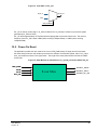
1.1.
USB Host Controller (UHOSTC) Block Diagram
Figure 1. USB Host Controller (UHOSTC) Block Diagram
OHCI
ROOT HUB
REGS
APP_SADR (6)
RCFG_RegData(32)
1
APP_SDATA (32)
CONTROL
HCI
USB
SLAVE
BLOCK
STATE
CONTROL
OHCI
REGS
PORT
S/M
ROOT
HUB
&
HOST
SIE
CONTROL
LIST
PROCESSOR
BLOCK
HCI BUS
USB
CONTROL
Cntl
HCI_DATA (32)
CONTROL
X
V
R
TxEnL
TxDpls
TxDmns
2
USB
PORT
S/M
X
1
V
R
Clock
Mux
12/1_5
CTRL
ED/TD _DATA (32)
HCM_ADR/DATA (32)
HCI
MASTER
BLOCK
ED & TD
REGS
ED/TD_STATUS (32)
RcvData
CTRL
HSIE
S/M
STATUS
APP_MDATA (32)
CONTROL
RcvDpls
ROOT HUB
CONFIG
BLOCK
RcvDmns
15
HC_DATA (8)
RH_DATA (8)
EXT. FIFO STATUS
DPLL
PORT
S/M
USB
X
V
R
DF_DATA (8)
FIFO_DATA (8)
HCF_DATA (8)
DF_DATA (8)
Addr(6)
64x8
FIFO
Cntl
FIFO
64x8
User Manual
October, 00
8
2.
HOST CONTROLLER CORE MAJOR FEATURES
Open HCI Rev 1.0 compatible.
USB Rev 1.1compatible.
RootHub is user configurable (e.g., Number of DownStreamPorts PowerSwitching Options etc.)
Support for both LowSpeed and HighSpeed USB Devices
No Bi-Directional or Tri-State Buses
No level sensitive Latches
Very simple Application Bus Interface
Support of SMI (System Management Interrupt) Pin
Hooks for Legacy Device Support
User Manual
October, 00
9
3.
HCI BUS APPLICATION INTERFACE BLOCKS
The HCI Bus is the interface between the inSilicon's Host Controller Core and the Application. This has
been defined as an easy to use FIFO based Interface. This has two parts: HCI-Master Interface and
HCI_Slave Interface.
HCI-Master handles all the Reads/Writes to System Memory, initiated by Host Controller. HC uses the
master interface for example, Writing/Reading Endpoint Data, Writing Status, Fetching ED, TD Data
Structures etc.
HCI_Slave Block implements OHCI Operational Registers. All the Reads/Writes to OHCI Registers happen
through this interface.
3.1.
HCI-Master Block
The HCI-Master block is the master on the HCI Bus. HCI Bus is defined to be as an interface between the
Host Controller and Applications. The HCI Bus will be discussed in more detail in the subsequent sections.
This block handles all the Reads/Writes initiated by Host Controller to System Memory. The following jobs
happen through HCI-Master Block.
Reading ED/TD from System Memory
Reading EndPoint Data from System Memory
Reading from HCCA
Writing Status & TD Retirement
Writing EndPoint Data to System Memory
Writing to HCCA
3.2.
HCI-Slave Block
The HCI-Slave block is the slave on HCI Bus. This is basically an interface between OHCI Operational
Register internal to HC and the Application. It updates the Registers on Writes and provides the Register
Data on Reads. All the slave accesses should be DWORD aligned. Therefore Byte Enables are not used in
Slave Accesses.
3.3.
The HCI Bus Signals and Protocol
The HCI Bus is the interface between the Host Controller Core and the Application. The Application's Host
Controller Interface should following the protocol defined in this section.
The HCI-Bus Interface signals are non tristate signals to be used internal to an ASIC or FPGA design.
These signals are meant to provide an easy way to use a FIFO style interface to the Application Bus (PCI,
etc.). For added convenience, all signals on the HCI-Bus are either input or output. There are no
bidirectional signals, which makes it easier to adapt designs to the HCI-Bus:
HCI bus is divided into two sections:
1. HCI-Master Interface
2. HCI-Slave Interface
Signal Notation:
User Manual
October, 00
The direction (I/O) is with respect to the Host Controller.
10
HCI_M***:
Signal source is the Host Controller's HCI Master Block.
APP_M***: Signal source is the Application Bus(PCI Etc.) Master(Slave on HCI Bus).
APP_S***: Signal source is the Application Bus(PCI Etc.) Slave(Master on HCI Bus).
APP_***:
Signal source is the Application Bus Master/Slave.
***_***N:
Signal is active low.
3.3.1.
HCI-Master Interface
The Host Controller is the master on this interface. All the transfers are initiated by the HC. All the signals
are nontristate, unidirectional. All the signals are nonmultiplexed except HCI_MAdrData on which System
Memory Address & Data are multiplexed. HC assumes that Application implements at least 4-deep 32-bit
wide FIFO for the Data. HCI Master is capable of bursting with the maximum burst length of 4 transfers (4
DWORDS).
The following table describes the HCI Master Interface Signals.
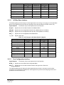
Table 2. HCI Master Interface Signals
SIGNAL
HCI_MAdrFInN
I/O
O
DESCRIPTION
HCI-Bus Master Address FIFO In. This is an active low signal and is used by
HCI Master to strobe the System Memory Address into the Application's
internal Address FIFO. If the application does not implement a FIFO for
Address, then this signal when asserted should be used as an Address Valid
Signal, and should Latch the Address into its internal Register. The Address
is placed on HCIM_AdrData multiplexed Bus. When HCIM_AdrFInN is valid
this Bus carries Address. This signal is synchronous to 12 Mhz Clk12. This
signal is one clock wide and should be sampled by the application on the
rising edge of Clk12. This Signal also qualifies HCIM_RdWr, which indicates
if the transaction is Memory Read or Memory Write.
As soon as Address is strobed in the Application's FIFO/Register,
Application should generate APP_MAFullN, because HC
assumes that the Address FIFO is only one deep (32-bit
wide). This signal should be kept asserted until the
application finishes the requested Read/Write. APP_MAFullN
inactive indicates the HC that the requested transfer is
finished. This means the Application should empty the
Address FIFO(making APP_MAFullN inactive) only after
strobing all the requested DWORDs into the Data FIFO for
Reads and after emptying all the DWORDs from Data FIFO
for Writes.
HCI_MAdrData[31:0]
O
HCI-Bus Master System Memory Multiplexed Address/Data. This signal
meets setup & hold time to the rising edge of Clk12 in the clock when the
HCIM_AdrFInN or HCI_MDataFInN signal is active. This bus carries Address
when HCIM_AdrFInN is active and carries Data when HCI_MDataFInN is
active.
The Application should start transferring the Data to/from System Memory as
soon HCIM_AdrFInN is valid.
When carrying Data, no byte swapping and no byte alignment is provided by
HC. The Applications that use other than 32-bit wide Bus need to have their
own byte swapping and byte alignment logic to interface to the HC.
HCI_MRdWr
User Manual
October, 00
O
HCI-Bus Master Read/Write Command: This indicates if the current
transaction is a Memory Read or Memory Write. This is a static signal and
asserted before the Address is strobed into address FIFO for Reads, before
the first data is strobed into the Data FIFO for Writes. This signal stays
asserted until the Address FIFO is emptied by Application.
11
Default value for this signal is '0' which indicates Read and toggles to '1' on
Writes.
0: Memory Read
1: Memory Write
HCI_MDataFInN
O
HCI-Bus Master Read/Write Data FIFO In. This is an active low signal and is
synchronous to the rising edge of Clk12.. When active, the application should
latch HCI_MAdrData[31:0], HCI_MBeN[3:0], and HCI_MWBurstOnN into its
internal Data FIFO. The Application can choose to implement separate
FIFO's for Data, Byte Enables, and BurstOn flag, or single 37-bit wide FIFO.
For every rising edge of Clk12 that this signal is sampled active low a new
HCI_MData will be clocked into the Master Data FIFO. HC asserts this signal
to clock in HCI_MData,HCI_MBeN and HCI_MWBurstOnN only while the
Application Data FIFOs are nonfull. The full/nonfull status of the Master Data
FIFOs is indicated via the FIFO status signals. The Application should be
capable of accepting the HC Data at the rate of every Clk12 as long as the
Data FIFOs are not Full.
HCI_MDataFOutN
O
HCI-Bus Master Read/Write Data FIFO Out: HC asserts this signal on
System Memory Reads. This signal is synchronous to 12Mhz Clk12. After
initiating the Read Cycle, HC expects 32-bit wide Data on APP_Mdata Bus on
every clock it that samples this signal asserted. HC asserts this signal for the
number of clocks equal to HCI_MBstCntr. HC asserts this signal for one
clock for every data after reading the data until required number of words are
read. That means first should be automatically available.
HCI_MBeN[3:0]
O
HCI-Bus Master Byte Enables. These are the Byte enables for the 32 bits of
Data. These are active low signals and when active indicates that the
corresponding data byte lane is valid. For example, HCI_MBeN[3] qualifies
HCI_MAdrData[31:24] and HCI_MBeN[0] qualifies HCI_MData[7:0].
These signals are used by the HCI-Bus Master to post the bytes it wants to
transfer to/from the System Memory. These signals are clocked into the
Application Data FIFO and hence meet setup & hold time to the rising edge of
Clk12 in the clock when the HCI_MDataFInN signal is active.
HCI_MWBstOnN
O
HCI-Bus Write Burst On. Indicates an ongoing burst write from the HC. On
the last data that is clocked into the FIFO, this signal is deasserted to indicate
the end of burst. This should be clocked along with data and byte enables.
HCI_MBstCntr[2:0]
O
HCI-Bus Read Burst Count: Number of DWORDS to be read from System
Memory(HCI Master reads a maximum of 4 DWORDS/16 Bytes) in single
Burst.
It is valid only when HCI_MAdrFInN is active(when the Address on
HCI_MAdrData is valid)
HCI_MIrqN
O
HCI-Bus General Interrupt: This is one of the two interrupts HC uses to
notify HCD when interrupt condition occurs. If the application bus is PCI this
should be tied to standard PCI Interrupt Pin.
HC uses this pin when HcControl.IR bit is set to zero.
HCI_MSmiN
O
HCI-Bus System Management Interrupt(SMI): This is one of the two
interrupts HC uses to notify HCD when interrupt condition occurs.
HC uses this pin when HcControl.IR bit is set to one.
This signal is used only when Legacy Support is provided. Current
version of the Core does not support legacy devices, hence
can be ignored. Refer to OpenHCI Specification Rev1.0a for
Legacy Specification.
HCI_MRmtWkp
User Manual
October, 00
O
Host Controller RemoteWakeUp: RemoteWakeup event occurred on one of
the down stream ports of the Root Hub. This will be asserted for one clock
when HC transits from Suspend to R esume state. At the same time an
interrupt also generated. This event could either be Upstream Resume
Signaling or Connect/Disconnect event while RootHub is suspended. This
signal will be generated only if RWE bit HcControl register is set by
12
signal will be generated only if RWE bit HcControl register is set by
Application
Application's action when this is asserted is implementation
specific and it is beyond the scope of OHCI Specification.
This is just the status signal and can't be used to stop/start the
clocks.
HCI_MSofN
O
Host Controller's New Frame: Host Controller asserts this signal for one
clock, whenever HC's internal Frame Counter (HcFmRemaining) reaches "0"
and it is in Operational State. At this time HcFmRemaining gets reloaded with
HcFmInterval. On the next clock the first bit of SOF (first bit of the Sync Field
for SOF Token) is sent on to the USB.
This signal is asserted to let the Application know about the new
Frame, and an SOF token is being sent on to USB.
Application does not need to take any action. HC generates
this signal only when it is in the Operational State and sending
SOF Tokens.
HCI_MBufferAccess
O
Host Controller Buffer Access Indication: When active indicates that
currently HC is accessing Data Buffer indicated by the TD. This is just the
status signal to let the Application know if HC is reading/writing data buffer
indicated by TD or reading/writing ED, TD descriptor etc. If this is set (1)
during the cycle on HCI Master Bus that indicates buffer fetch and if reset (0)
all other transfers(ED,TD fetch, StatusWriteBack etc.)
This is just the status signal and Application need not take any
action when asserted.
HCI_MFClrN
O
Host Controller FIFO Clear Signal: HC asserts this signal when USB Reset
(when HcControl.HCFS is set to "00") or SoftWare Reset
(HcCommandStatus.HCR is written '1') is issued by Application
(HostControllerDriver) while HCI Master is either in the middle of a cycle or
just about to start a cycle. When asserted, it indicates that HC can no longer
start/continue the cycle and Application should terminate the transfer
gracefully and should clear both the Address and Data FIFOs. Once
asserted, this signal will stay asserted until HC re-enters the Operational State
which is a minimum of 10us that Application (HCD) should wait before HC is
forced directly to Operational state from Suspend.
On the HC write cycle, if HC has already strobed the Address into Address
FIFO, when this signal is asserted then it is up to the Application whether to
transfer the posted data or not.
If address is not already posted, then Application should simply clear the Data
FIFO.
On the HC read cycle, if HC has already strobed the Address into Address
FIFO, again it is up to the Application whether to read the data or not, but HC
won't empty the data FIFO and the Application should clear both the FIFOs.
APP_MAFullN
I
Application Address FIFO Full: The HC asserts HCI_MAdrFInN only when
this signal is inactive.
Host Controller assumes that the application will have one and only
one deep FIFO for Address Storage (32-bit wide, 1 deep).
Also Application should empty the FIFO only after the
requested transfer is done, because once the transaction is
started (after HC strobed the Address into the Address FIFO),
Address FIFO being empty indicates the HC that the
requested transfer is over.
APP_MDLastN
User Manual
October, 00
I
Application Data FIFO Last Entry: This signal active indicates to the HCI
Master that only one more entry is available in the Application Data FIFOs.
13
Master that only one more entry is available in the Application Data FIFOs.
That means as soon as HC writes one more data the FIFO becomes FULL.
If the HC needs to clock in data every clock (Burst Write), it monitors both
APP_MDFLastN & APP_MDFFullN.
APP_MDFullN
I
Master Data FIFO Full: This signal being active indicates to the HCI Master
that the Application Data FIFO is full.
If the HCI Master needs to clock in data every clock (Burst Write), it needs to
monitor both APP_MDFLastN & APP_MDFFullN.
APP_MDFirstN
I
Application Data FIFO First Entry: This signal active indicates to the HCI
Master that only one more entry is available in the Application Data FIFOs.
That means as soon as HC reads one more data FIFO becomes EMPTY
If the HC needs to clock out data every clock (Burst Read), it monitors both
APP_MDFFirstN & APP_MDFEmptyN.
APP_MDEmptyN
I
Application Data FIFO Empty: This signal active indicates to the HCI Master
that the DFIFO is empty and should not assert the Read Strobe.
APP_MSysErrN
I
Application System Error: When a fatal error occurs on the Host Bus and if
the application cannot start/finish the transfer initiated by HC for any reason
this signal should b e asserted by the Application. Also application needs to
clear its internal Address and Data FIFOs. This signal should be asserted for
at least 4 clocks from the time Application clears the Address FIFO. That
means HC understands it to be a fatal condition when it samples this signal
asserted along with the Address FIFO Full signal (APP_MAFullN)
inactive(empty). And this signal should stay asserted for 3 more clocks after
HC samples APP_MAFullN inactive.
Examples of fatal errors (not recoverable) for PCI Bus:
Target Abort
Address Parity Error
Master Abort
When the HC samples this signal asserted, it sets
HcInterruptStatus.UE (UnRecoverableError) and generates an
Interrupt to HCD. HC does not process any lists until this is
cleared by HCD by setting HcCommandStatus.HCR(Host
Controller Soft Reset)
APP_MData[31:0]
I
Application Data to the HCI-Master. These are the System Memory Data
clocked out of the Application's Data FIFO on Reads.
Since this signal is nonmultiplexed, HCI Master assumes that the first data is
valid and available as soon as APP_MDFEmptyN goes inactive on System
Memory Reads. After latching this Data into HC's internal Registers/FIFOs
etc, HCI Master asserts HCI_MDataFOutN so that Application increments
FIFO's Read Counter, and Empty signal is still inactive, that means that the
next Read Data is available to HCI-Master in the case of Burst Transfer.
APP_RstN
I
Application PowerOnReset to Host Controller. This is PowerOnReset to
HC and should be asserted for at least 4 clocks of 1.5 Mhz. HC synchronizes
this signal to all the local clock domains before using.
APP_ScanModeN
I
Application Scan Mode Select to Host Controller. This signal is intended
to provide the hooks if scan chain is implemented. When asserted, entire HC
will run on Clk12 primary I/P.
APP_ClkCktRstN
User Manual
October, 00
Initial reset signal for DPLL (rh_pll module) block. This is only needed for
simulation and can be tied inactive in the real netlist. This signal will be used
by the flip-flops tht extract pll_clk from the incoming data. See the description
for the HCI Master bus signal for the relative timing of this signal with respect
to the system reset APP_RstN signal.
14
APP_LegacySupport
3.3.2.
I
Application Legacy Support Indication. If Application chooses to
implement Lagacy Support logic outside the Core it should be tied to '1'. It
should be tied to '0' otherwise. This bit is returned as part of the HcRevision
register when it is read at offset 00 of OHCI Registers. Refer to OpenHCI
Specification Rev1.1 for Legacy Specification.
HCI-Slave Interface
The Host Controller is slave on this interface. All the transfers are on this interface are initiated by the Host
Controller Driver (HCD) through the Application Bus typically PCI. HCD uses this interface to program the
on chip Operational Registers (HCI Regs.) of the Host Controller.
The following table describes the signals used on HCI Slave Interface.
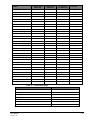
Table 3. HCI Slave Interface
SIGNAL
HCI_SData[31:0]
I/O
O
DESCRIPTION
HCI Register Read Data: This is th e Data returned by HCI Slave on Reads from the
Application. Read Data is valid & available to the Application whenever the Address
changes. For example if the Application asserts the new Address on 5 th Clock it
can Latch/Register the Data on 6 th Clock.
APP_SAdr[5:0]
I
HCI Register Address. These are the HCI Register Address used by the
Application when Reading/Writing Register Data. This is not the absolute address,
just the offset of the OHCI Registers internal to the Host Controller.
APP_SDataRdyN
I
HCI Register Write Data Valid: The Application should assert this signal when the
Address, and Data to be written to HC's Operational Registers is valid. Data is
written into the Registers when HC samples this signal asserted on the rising edge
of Clk12.
APP_SData[31:0]
I
HCI Register Write Data: Data to be written into HC's Operational Registers.
APP_SReadN
I
HCI Register Read Strobe: The Application needs to assert this signal for one clock
along with the valid address when reading the OHCI Registers.
APP_SAdr should meet setup time to Clk12.
This signal is currently not used by HC, but it is defined incase future
revisions of OHCI Specification if any requires that HC sense the
Read for example any new bits in the OHCI Registers that need to
be cleared/set on Reads.
So current implementation is not sensitive to APP_SReadN but it is sensitive to
APP_Sadr. Read Data is available one clock after the Address on APP_Sadr
changes. As long as the Address is not changed, HCI_Sdata reflects the contents
of the OHCI Registers pointed to by APP_Sadr offset.
User Manual
October, 00
15
4.
FIFO INTERFACE
This is the interface between the Host Controller's internal FIFO Controller and the 64x8 FIFO. The idea
behind separating the FIFO from the rest of the blocks is that you can replace the Flip-Flop based FIFO
source code provided by inSilicon with your own custom RAM Block to cut down the Gate count.
The following table describes the signals on this Interface. The direction is with respect to the FIFO Block.
Signal Notation:
The direction (I/O) is with respect to the Host Controller.
HCF_***:
Signal source is the Host Controller's Fifo Controller
FIFO_***
Signal source is the FIFO Block
***_***N:
Signal is active low.
Table 4. Interface Signals
SIGNAL
I/O
Clk12
I
HCF_WriteN
I
HCF_WrPtr[5:0]
I
HCF_RdPtr[5:0]
I
HCF_Data[7:0]
I
FIFO_Data[7:0]
O
User Manual
October, 00
DESCRIPTION
12 Mhz Clock All the Reads/Writes are synchronous to this System
Clock(This is also a primary input to the Host Controller)
FIFO Write Strobe Write Data Valid. When this signal is sampled
asserted on Clk12, FIFO Block writes the Data on HCF_Data bus into
the location specified through HCF_WrPtr
Write Data Address Address of the FIFO/RAM Block location to
which HCF_Data is copied when HCF_WriteN is asserted
Read Data Address. Read Address of the FIFO/RAM Block. Read
Data at the location pointed to by HCF_RdPtr is always appears on
the FIFO_Data Bus.
FIFO Write Data. Data to be written into FIFO/RAM Block. Write
Data on this bus is written into the location pointed to by Address
"HCF_WrPtr" when HCF_WriteN is sampled asserted on the rising
edge of Clk12.
FIFO Read Data. Data returned on FIFO Reads. This bus always
carries the data in FIFO location pointed to by HCF_RdPtr
16
5.
USB PORT INTERFACE
This is the Interface between Host Controller's RootHub Config Block and DownStream USB Port
Transceivers. The following table describes the Signals on this Interface.
Width of the signals on this bus depends on NDP (Number of DownStream Ports) that is user
programmable.
Table 5. USB Port Interface Signals
SIGNAL
I/O
PRT_RcvData
[NDP-1:0]
PRT_RcvDpls
[NDP-1:0]
I
PRT_RcvDmns
[NDP-1:0]
I
PRT_OvrCurrent
[NDP-1:0]
I
I
DESCRIPTION
Receive Data from USB Port Transceiver. This is the receive
signal generated from D+, D- differential lines of USB Cable
NRZI Encoded Dpls (D+) from USB Port Transceiver. This is the
D+ signal from the USB Ports. This along with PRT_RcvDmns is
used to detect connect/disconnect condition and
SingleEndedZero(SE0)
NRZI Encoded Dmns (D+) from USB Port Transceiver. This is the
D- signal from the USB Ports. This along with PRT_RcvDpls is used
to detect connect/disconnect condition and SingleEndedZero(SE0)
OverCurrent Indication from Application. When asserted by
Application the corresponding Port will enter DISCONNECT state if
PowerSwitching is not implemented or PoweredOff state if
PowerSwitching is implemented irrespective of its present state.
In either case, this signal should be cleared before that Port can be
reused. Besides if PowerSwitching is implemented, Power needs to
be turned on(by writing to OHCI Registers) before Port detects
connect event of any peripheral downstream.
Also when this signal is asserted, HC sets either
HcRhPortStatus.POCI(if PowerSwitchingMode is PerPort) or
HcRhStatus.OCI(if PowerSwitchingMode is Global) if OverCurrent
Protection is supported(HcRhDescriptorA.NOCP is cleared).
If any of the above two bits are set(OCI or POCI) and PowerSwitching
is implemented(HcRhDescriptorA.NPS is cleared) then
HcRhPortStatus.PPS(PortPowerStatus) is cleared which causes the
Port enter PoweredOff state.
Another condition where this signal is used is GangedModePower
Switching. Ports are said to be in a GANG if PowerSwitchingMode is
PerPort(HcRhDescriptorA.PSM is set) and the corresponding
HcRhDescriptorB.PPCM bit is cleared. In this case if
OverCurrentCondition exists on any Port, PPS bits of all the Ganged
Ports are cleared provided PowerSwitching is implemented. But
OverCurrentCondition(OCI) bit set for only Ports whose
PRT_OvrCurrent signal is set.
This signal can be asynchronous as it is double synchronized
internally to Clk12
For more information refer to OpenHCI Specification Rev1.0 Section
7.4.
RCFG_txdPls
[NDP-1:0]
User Manual
October, 00
O
NRZI Encoded Dpls(D+) to USB Port Transceiver. This is the D+
signal to the Transceiver at the USB Ports.
17
SIGNAL
I/O
RCFG_txdMns
[NDP-1:0]
RCFG_txSe0 [NDP1:0]
O
RCFG_txEnL [NDP1:0]
RCFG_speed
[NDP-1:0]
RCFG_suspend
[NDP-1:0]
RCFG_PrtPower
[NDP-1:0]
O
RCFG_GlobalSuspe
nd
O
O
O
O
O
DESCRIPTION
NRZI Encoded Dmns(D-) to USB Port Transceiver. This is the D+
signal to the Transceiver at the USB Ports.
This signal is generated from original source signals that move D+/Dlow during SEO conditions. It is used by external transceivers to drive
SEO on USB. Using this signal is optional for transcievers.
RCFG_txdPls and RCFG_txdMns are also driven low during SEO as
usual.
Transmit Enable to USB Port Transceiver. This is the Enable
signal to the Transceiver at the USB Ports.
Transmit Speed to USB Port Transceiver. This signal indicates if it
is a High Speed or Low Speed transmission
Port Suspend Signal. This signal indicates the state of the port.
Suspend/Active.
Port Power Indication (On:1/Off:0). This signal always reflects the
HcRhPortStatus.PPS (PortPowerStatus) bit of the respective Port.
HC is in GlobalSuspend State. This signal is asserted 5 ms after
HC enters USBSUSPEND State. Once asserted, it stays asserted as
long as HC remains in this state. HC enters USBSUSPEND state
when HCD(HostControllerDriver) forces it by writing to
HcControl.HCFS bits. And HC exits this state when either HCD
moves it to USBRESET(GlobalUsbReset) or
USBRESUME(GlobalResume) or when a RemoteWakeUp event is
seen at one of the downstream USB Ports.
This is just a status signal and Application need not use it for
normal operation. This information can be used if Clock
Start/Stop logic (during GlobalSuspend) external to the
UHOSTC Core is implemented.
RCFG_DRWE
O
DeviceRemoteWakeupEnable. This signal reflects
HcRhStatus.DRWE bit. This signal when active causes HC to treat
Connect/Disconnect event as RemoteWakeUp which in turn causes
HC to enter GlobalResume State from GlobalSuspend State. If this
bit is cleared Connect/Disconnect event is not treated as
RemoteWakeUp event.
This is just a status signal that helps in Clock Start/Stop logic. This
signal can be ignored for normal operation of the UHOSTC
Core.
RCFG_CCS[NDP1:0]
O
Current Connect Status of each Port. This bit when active indicates
that the Port S/M is in CONNECTED state. If this bit is cleared then
the Port S/M is in either DISCONNECTED state or PoweredOff State.
This is just a status signal and Application can ignore this for the
normal operation of UHOSTC Core. This is also used in
external Clock Start/Stop Logic.
RCFG_RWE
User Manual
October, 00
O
RemoteWakeUp enabled. This bit reflects HcControl.RWE bit. This
is brought out as just a status signal and can be ignored by the
Application for normal operation of the UHOSTC Core.
18
6.
LIST PROCESSOR BLOCK
The list processor block acts as a main controller of the entire core. It has multiple State Machines to
implement List Service Flow, List Priority, USB-States, ED,TD Service, StatusWriteBack, TD Retirement etc.
as per the OHCI Specification. In addition to that this block implements a controller which interfaces with
hci_master and hsie, helping them in the data transfer from System Memory to USB and USB to System
Memory.
It has the following submodules.
USB States
List Service Flow
ED-TD Block
HCI-Master Interface Logic
Data Read Write Logic
The following sections explain about each submodule in detail. Some of the information in this section is
reproduced from the OHCI Specification for easy reference.
6.1.
USB States
This is the top-level block in the list processor hierarchy. It is directly controlled by the OHCI Registers, and
this block has the main S/M triggers all the other lower level S/Ms. This S/M implements the Host Controller
States visible to the USB as defined in the OHCI Specification. In addition to that this S/M also implements
the logic which generates the control signals to transmit SOF Tokens, Reset/Resume, and writing the
FrameNumber for every 1-ms back to the HCCA in the System Memory. This block has another S/M to
implement DoneQueueCounter.
While in the Operational State, every frame after finished sending the SOF Token, it triggers the List Service
Flow S/M, which services the lists scheduled by HCD. After the scheduled work is done in the current
frame, List Service Flow S/M returns control back to this S/M. This sequence is repeated for every Frame
(1ms).
The Host Controller has four USB states visible to the Host Controller Driver via the Operational Registers:
USBOPERATIONAL, USBRESET, USBSUSPEND, and USBRESUME. These states define the Host Controller
responsibilities relating to USB signaling and bus states.
The USB states are reflected in the HostControllerFunctionalState field of the HcControl register. The Host
Controller Driver is permitted to perform only the USB state transitions shown in Figure 2. The Host
Controller may only perform a single state transition. During a remote wakeup event, the Host Controller
may transition from USBSUSPEND to USBRESUME.
User Manual
October, 00
19
Figure 2. USB States of the Host Controller
USB OPERATIONAL
USB RESET write
USB OPERATIONAL
USB OPERATIONAL
write
write
USB RESUME
USB RESET write
USBR ESET
USB SUSPEND write
USB RESUME write
or
Remote Wakeup
USB RESET write
Hardware Reset
USB S USPEND
Software Reset
6.1.1.
UsbOperational
When in the USBOPERATIONAL state, the Host Controller may process lists and will generate SOF Tokens.
The USBOPERATIONAL state may be entered from the USBRESUME or USBRESET states. It may be exited to
the USBRESET or USBSUSPEND states.
When transitioning from USBRESET or USBRESUME to USBOPERATIONAL, the Host Controller is responsible
for terminating the USB reset or resume signaling as defined in the USB Specification prior to sending a
token.
A transition to the USBOPERATIONAL state affects the frame management registers of the Host Controller.
Simultaneously with the Host Controller's state transition to USBOPERATIONAL, the FrameRemaining field of
HcFmRemaining is loaded with the value of the FrameInterval field in HcFmInterval. There is no SOF
Token sent at this initial load of the FrameRemaining field. The first SOF Token sent after entering the
USBOPERATIONAL state is sent following next frame boundary when FrameRemaining transitions from 0 to
FrameInterval. The FrameNumber field of HcFmNumber is incremented on a state transition to
USBOPERATIONAL.
6.1.2.
UsbReset
When in the USBRESET state, the Host Controller forces reset signaling on the bus. The Host Controller's
list processing and SOF Token generation are disabled while in USBRESET. In addition, the FrameNumber
field of HcFmNumber does not increment while the Host Controller is in the USBRESET state. The
USBRESET state can be entered from any state at any time. The Host Controller defaults to the USBRESET
User Manual
October, 00
20
state following a hardware reset. The Host Controller Driver is responsible for satisfying USB Reset
signaling timing defined by the USB Specification.
6.1.3.
UsbSuspend
The USBSUSPEND state defines the USB Suspend state. The Host Controller's list processing and SOF
Token generation are disabled. However, the Host Controller's remote wakeup logic must monitor USB
wakeup activity. The FrameNumber field of HcFmNumber does not increment while the Host Controller is
in the USBSUSPEND state.
USBSUSPEND is entered following a software reset or from the USBOPERATIONAL state on command from the
Host Controller Driver. While in USBSUSPEND, the Host Controller may force a transition to the USBRESUME
state due to a remote wakeup condition. This transition may conflict with the Host Controller Driver initiating
a transition to the USBRESET state. If this situation occurs, the HCD-initiated transition to USBRESET has
priority. The Host Controller Driver must wait 5 ms after transitioning to USBSUSPEND before transitioning to
the USBRESUME state. Likewise, the Root Hub must wait 5 ms after the Host Controller enters USBSUSPEND
before generating a local wakeup event and forcing a transition to USBRESUME. Following a software reset,
the Host Controller Driver may cause a transition to USBOPERATIONAL if the transition occurs no more than 1
ms from the transition into USBSUSPEND. If the 1-ms period is violated, it is possible that devices on the bus
will go into Suspend.
6.1.4.
UsbResume
When in the USBRESUME state, the Host Controller forces resume signaling on the bus. While in
USBRESUME, the Root Hub is responsible for propagating the USB Resume signal to DownStream ports as
specified in the USB Specification. The Host Controller's list processing and SOF Token generation are
disabled while in USBRESUME. In addition, the FrameNumber field of HcFmNumber does not increment
while the Host Controller is in the USBRESUME state.
USBRESUME is only entered from USBSUSPEND. The transition to USBRESUME can be initiated by the Host
Controller Driver or by a USB remote wakeup signaled by the Root Hub. The Host Controller is responsible
for resolving state transition conflicts between the hardware wakeup and Host Controller Driver initiated
state transitions. Legal state transitions from USBRESUME are to USBRESET and to USBOPERATIONAL.
The Host Controller Driver is responsible for USB Resume signal timing as defined by the USB
Specification.
6.2.
List Service Flow
This block implements the S/M to service the lists scheduled by HCD according to the priority programmed
in OHCI Operational Registers. This S/M is triggered by the USB States S/M in every frame after SOF is
sent on to USB. Once it determines which list to serve, it triggers EDTD (ETD) S/M to serve one packet
from that list. At the end of the packet transfer, ETD S/M returns the control back to this S/M. This
sequence is repeated for every packet, and every list until the scheduled work is done for the current frame
or until the EndOfFrame (EOF). At the EOF control is returned back to USB States S/M.
This block also implements the priority algorithm. This includes the determination of which list
(periodic/nonperiodic) list currently needs to be processed based on the contents of the appropriate HCI
Regs. With in the nonperiodic list it determines what type of transfer currently needs to be done (Control or
Bulk) based on the 'Control Bulk Service Ratio (CBSR)' of the HCI Regs.
On a cue from the Priority Algorithm, the List Service Flow State Machine (LSF S/M), processes that data
structure to establish whether an ED Descriptor exists to be processed. If no ED Descriptor exists, the LIST
State Machine indicates this to the Priority Algorithm. If an ED Descriptor does exist, then the LIST State
Machine provides the necessary information to the ED State Machine to process the ED.
The flow chart shown below is a description of the LIST State Machine to establish whether an ED
Descriptor exists to be processed.
User Manual
October, 00
21
Figure 3. List Service Flow Diagram
SERVICE
LIST
Read
HEAD pointer
YES
Peridoc List?
YES
List
Enabled?
NO
FINISHED
____Filled = 1?
(Bulk or Control)
YES
Set
Hc____CurrentED =
Hc____HeadED
NO
HEAD pointer
= 0?
Hc____CurrentED
= 0?
YES
NO
NO
Set
____Filled = 0
ISOCHRONOUS
ED?
NO
NO
YES
FINISHED
YES
YES
Hc____CurrentED
= 0?
NO
ISO List
Enabled?
YES
Service Endpoint
Descriptor
NO
YES
NO
FINISHED
YES
YES
Control/Bulk
Ratio Satisfied?
YES
BULK List?
ISOCHRONOUS
ED?
NO
NO
CONTROL LIst?
NO
NextED = 0?
YES
ISO List
Enabled?
NO
YES
FINISHED
NO
6.3.
ED-TD Block
This block gets triggered by LSF S/M for every packet transfer. The logic of the S/M (ETD S/M) in this block
can be divided into the following two functional blocks.
6.3.1.
ED Block
The ED State Machine Block gets its cue from the LIST State machine. The purpose of the ED State
Machine is to determine it there is a TD Descriptor that needs to be processed. If a TD Descriptor is not
available, then the ED State machine indicates this to the LIST State Machine. If a TD Descriptor does
User Manual
October, 00
22
exist, then the ED State Machine provides the necessary information to the TD State Machine to process
the TD.
The flow chart shown below is a description of the ED State Machine to establish whether a TD Descriptor
exists to be processed.
Figure 4. ED Service Flow Diagram
SERVICE
ENDPOINT
DESCRIPTOR
HALT = 1
or
SKIP = 1?
NO
NextTD =
Tail Pointer?
NO
Periodic List?
NO
Set
____Filled = 1
(Bulk or Control)
YES
YES
YES
Service
Transfer Descriptor
FINISHED
The TD State Machine acts on the information provided by the ED State Machine. After fetching the TD
Descriptor from system memory, the TD State Machine block interfaces with the Framing block and the
Address & Size Calculation blocks to determine if this is the right Frame number for Isochronous frames and
if there is sufficient frame time available (in the 1ms frame period) to be able to successfully transfer this
data to the USB device. If the checks for Frame number and Transfer time required is OK, then the TD
State Machine initiates a USB transfer by interfacing to the Root Hub/SIE Blocks via the Read/Write FIFOs.
If the checks are not OK no USB transfer is initiated.
At the end of the successful or not successful USB transfer, the TD passes control to the Status Write Back
Block, which updates the Status in the System Memory.
The following is a flow chart showing the process of a TD Descriptor.
User Manual
October, 00
23
Figure 5. TD Service Flow Diagram
SERVICE
TRANSFER
DESCRIPTOR
ITD
Compare Number with
Frame in ED
Frame - Number
> N?
YES
(Error)
GTD
NO
Calculate PACKET
Addr and Size
PID = OUT?
NO
(Frame - Number
provides Offset)
Frame - Number
< 0?
Read PACKET
from memory
Perform SOF check
YES
YES
(Early)
NO
Perform SOF check
Time available?
NO
YES
Time available?
Execute USB
Transaction
YES
Execute USB
Transaction
Write PACKET
to memory
NO
Status Writeback
TD Complete?
NO
FINISHED
YES
Retire TD
6.3.2.
HCI -Master Interface Logic
This block acts as an interface between HCI-Master section of the HCI bus and the various other blocks of
the Host Controller. These other blocks include ED,TD,List Service Flow, etc. All the writes and reads
to/from PCI bus go through this block. It implements Address/Data MUX, which generates the Address,
Data for various Reads/Writes to/from System Memory. It also implements the registers necessary store
User Manual
October, 00
24
ED (4 DWORDs) and TD (8 DWORDs) data structures fetched from the system memory. In addition to that
this block implements the following two tasks.
6.3.2.1.
Status WriteBack
When the TD state machine is done transferring the data from/to the USB, the Status Write Back block
updates the system memory with a report of the transfer.
6.3.2.2.
TD Retirement
When all the data specified by a TD has been transferred successfully or an error has occurred, the TD
retirement block moves the TD descriptor onto the TD Done queue.
6.3.2.3.
Address & Packet Size Calculation
This block performs the Address and Packet Size Calculation for the TD s. This information is passed to the
TD State Machine for transfers onto the USB Bus.
6.4.
Data Read Write Logic
The Data Read Write (DRW) Logic Block implements a S/M to transfer the data between USB & System
Memory. It synchronizes HSIE and HCI-Master.
On IN Packet, as data is received from the EndPoint, SIE stores it in DFIFO. When all the data is
received(for GTD/ITD) or data in the DFIFO is above a certain threshold( >= 16 bytes), ETD S/M triggers
this S/M by issuing a write command. Starting address of the write is provided by HCI-Master Interface
Logic Block. This S/M then triggers the HCI-Master to do a write cycle, by providing the address, and
number of bytes. If the number of bytes to be written is more than 16 bytes, it does multiple cycles, each
cycle with 16-bytes and the last cycle with the remaining bytes. It increments the address accordingly for
every cycle. It repeats this sequence until it sees RH_HskRdy, which indicates that all the data is received
from the USB, then it stops the write cycles as soon as DFIFO empty. At the end of the transfer, it returns
the control to ETD S/M.
Similarly on OUT Packets, ETD S/M triggers this S/M to read the data from the System Memory. The
address and the number of bytes to be read are provided by HCI-Master Interface Logic Block. Again it
does multiple cycles through HCI-Master if the data to be read is more than 16-bytes. At the end of the
transfer it returns the control back to the ETD S/M.
The addresses, and number of bytes that this block generates are routed to HCI-Master Block via HCIMaster Interface Logic Block, where these gets multiplexed with the address & data that the HCI_Master
Interface Logic generates. This S/M only handles reads/writes of the data related to EndPoint. All the other
reads/writes (StatusWriteBack, Reading of List HeadPointers, etc.) are handled by HCI-Master Interface
Logic Block.
User Manual
October, 00
25
7.
HCI-MASTER BLOCK
HCI-Master Block is the interface between HCI-Master Interface Logic Block and HCI Bus. It converts all
the cycles initiated by different blocks of the list processor through HCI-Master Interface Logic Block into
HCI-Bus cycles according to the protocol defined for HCI-Bus. In addition to that it implements a S/M to
read/write from/to DFIFO. When it is transferring the data returned by EndPoint, it clocks out the data from
DFIFO and merges into DWORD and then clocks it into the Application's internal FIFO. Similarly when
reading the EndPoint Data from the System Memory, after reading every DWORD from the Application's
FIFO it splits the DWORD into 4 individual bytes and then clocks it into the DFIFO. It also implements bytealignment logic, that is when a write cycle is initiated by FMLogic Block at the odd boundary (not the
DWORD boundary), it readjusts the lower 2-bits of the address (ties them to "0"), so that the Application
always writes at DWORD boundary, and manipulates the byte-enables accordingly.
User Manual
October, 00
26
8.
ROOTHUB AND HSIE BLOCKS
Most of the functionality of the RootHub is implemented in the Port Configuration Block, because it varies
with the implementation. The logic that is implemented here is common to any user configuration. The logic
in this block acts as a wrapper around HSIE and interface with Host Controller's List Processor, FIFO and
OHCI Registers. This block also implements the control logic to synchronize the interface between HSIE
and Port S/Ms.
8.1.
RootHub and HSIE Submodules
This Block implements the following submodules:
Reset_Resume
Dpll
HSIE
8.1.1.
Reset_Resume
This block implements a S/M to generate Low Speed Keep Alive signal which is broadcasted to all Low
Speed Ports while SOF is being sent to Full Speed Ports. This is needed to keep low speed ports alive
because SOFs are not decoded by low-speed ports. This block also implements a counter that runs on
12Mhz clock and generates a pulse of one clock wide for every one millisecond. This pulse is used by the
Reset/Resume counters in the Port Configuration Block to count Reset/Resume timing etc.
8.1.2.
Digital PLL Block (DPLL)
The function of the DPLL Block is to extract the clock and data information from the USB Data received from
the differential transceiver. The Digital PLL runs on a 48 MHz user-provided clock to extract the clock
information from the USB for both FullSpeed and LowSpeed data. The two signals D+ and D- of the USB
lines are passed through a differential receiver (external to the UHOSTC Core) and a NRZI formatted data is
obtained from the output of the differential receivers. The output of the differential receiver is then used by
the Digital PLL to extract clock information. The PLL Block also has a SE0 Detect Logic to detect the Single
Ended Zero(SE0) in the data stream. The circuit in this module extracts clock from either HighSpeed data
or LowSpeed data indicated by SIE_SwitchClk input from SIE Tx S/M. PonRst is the PonRst_ClkCkt_Clk48
signal that is derived from APP_ClkCktRstN. APP_ClkCktRstN is the primary input to the core, and it
serves as the initial reset to the flip-flops that generate the extracted pll_clk. The pll_clk is used by the
receiver block in the HSIE to sample pll_data.
User Manual
October, 00
27
Figure 6. DPLL Block Diagram
DPLL BLOCK
Clk48
pll_clk
PonRst
pll_data
Digital PLL
SIE_SwitchClk
pll_se0
SIE_Idle
data_in
dpls
dmns
SE0 Detect
8.1.2.1.
Signal Description for DPLL Block
The following explains the Signals going to the DPLL Block. All the signals are High ('1') asserted signals
unless otherwise specified.
Table 6. DPLL Block Signals
SIGNAL NAME
DIRECTION
Clk48
I
PonRst
SIE_Idle
data_in
dpls
dmns
pll_clk
I
I
I
I
I
O
pll_data
O
pll_se0
O
8.1.3.
DESCRIPTION
48Mhz primary Clock I/P used as over sampling clock to
extract PLL_Clk(12Mhz or 1.5Mhz) from USB Data Stream
PowerOnReset synchronized Clk48
SIE Tx S/M is Idle
Differential Data line from Port MUX.
D+ serial line from Port MUX
D- serial line from Port MUX
This is the extracted clock from DPLL. Data receiver in HSIE
should sample D+, D- lines on this clock. This is either 12 or
1.5Mhz generated based on the Clk_4x reference clock and
D+,D- lines from the Port MUX
Differential data (data_in) received from Port MUX is double
synchronized with Clk_4x and sent out as pll_data
SingleEndedZero extracted from dpls,dmns lines
Functionality/DataPath of the HSIE
The functionality of the Host Serial Interface Engine (HSIE) is to receive and transmit the USB data over D+
and D- lines in accordance with the USB protocol. During the reception of USB data, the D+ and D- signals
User Manual
October, 00
28
are passed through the differential receiver (which is external to the UHOSTC Core) to get a single ended
bit stream that is passed though the PLL Block to extract the clock and data information. The Clock and data
are passed to the SIE Block to identify the Sync Pattern and for NRZI-NRZ conversion. This NRZ data is
then passed through the Bit Stripper which strips of the excessive 0's inserted. The data stream is initially
passed through the PID Decode and checker to identify different PID's. Depending upon the type of PID,
the HSIE Block handles the protocol accordingly. If it is a Data PID, the serial data is assembled into byte
format and the CRC of the received data is calculated on the fly as data is received and then stored into the
DFIFO. The Data Flow diagram of the Receive Engine is shown below.
Figure 7. Receive Data Path of HSIE
From Diff. Xver
DPLL
Sync Field
Identifier
NRZI- NRZ
Data/CRC
Checker
Serial to
Parallel
Bit
Stripper
To DFIFO
PID decode
Check
HandShake
Checker .
The SIE Block takes the data from the DFIFO in the byte format and converts it into serial data. Bit Stuffing
is performed on this data and the data is converted from NRZ format to the NRZI format and transmitted to
the USB. The data is passed through the Differential Driver (which is external to UHOSTC) before going on
to the USB Cable. In case of HandShake packet the SIE Block assembles the appropriate HandShake
packet and sends it out to the USB. The data flow diagram for the transmit engine is shown below.
User Manual
October, 00
29
Figure 8. Transmit Data Path of HSIE
To Diff. Driver
NRZ to
NRZI Conv
Bit
Stuffing
Token
Assembler
Token &
CRC5
Generator
HandShake
Generator
M
U
X
DFIFO
64X8
CRC16
Generator
HSIE has the following three submodules:
Receive Block
Async Block
Transmit Block
These blocks are described in the following sections.
8.1.3.1.
Receive Block
All the logic in this block runs on the pll_clk extracted by DPLL from the received serial data. This block
implements most of the receiver functions like sync-field detection, NRZI-NRZ conversion, bit stripping, SE0
detection, CRC16 calculation, time-out logic, serial-to-parallel conversion etc. This block also implements a
S/M to detect the if valid hand shake is received by the functions on USB. All the signals that are output
from this block are synchronous to pll_clk and they are resynchronized to Clk-1x in Async Module and then
sent to Transmit Block which implements the main HSIE protocol.
8.1.3.2.
Async Block
This is just a synchronization block between Receive & Transmit blocks. This block synchronizes all the
control signals going back & forth between Receive & Transmit blocks. All of the signals going from
Receive block to Transmit block are synchronized to Clk_1x, and all the signals going from Transmit block
to Receive block are synchronized to pll_clk.
8.1.3.3.
Transmit Block
All the logic in this block runs on Clk_1x(12Mhz or 1.5Mhz) and implements the main SIE State Machine
and other logic. This block is the interface between Host Controller and Port Configuration Block. This
block is responsible for sending Token, Data, and HandShake packets and receiving Data packets. This
block implements the logic for parallel-to-serial conversion, bit-stuffing, NRZ-NRZI conversion, CRC5,
CRC16 calculation. All the control signals that are input to this block from Receive Block are synchronized
to Clk_1x in the Async Block.
User Manual
October, 00
30
The Transmit Block gets triggered when the List Processor asserts HC_TknReady indicating that a packet is
ready to be transmitted/received. List Processor passes all the information needed to assemble Token/Data
packets, for example Function Address, EndPoint Number, Token PID, Data PID etc. Now the SIE sends
the token packet on to USB, and either expects Data Packet (IN Token) or sends the Data Packet
(OUT/SETUP Token). On IN token, as data is received, SIE strobes the data into the DFIFO and
increments its internal counter to count the number of bytes received. At the end of the packet reception
(including EOP), it sends the HandShake packet on to USB, if the current packet is not the Isochronous
Packet, and received packet is error free or times out.
On an OUT or SETUP packet, similar to the IN packet, it sends out token packet and then sends the data
packet with the Data PID provided by the List Processor. Number of bytes to be sent is also provided by the
List Processor. At the end of the packet transmission, it waits for the handshake from the USB (if the
current packet is not an Isochronous Packet).
At the end of the every packet transmission HSIE asserts the handshake signal (RH_HskRdy) for one clock,
indicating that the packet transfer initiated by the List Processor is completed. Along with the handshake, it
returns the completion status (Refer to OHCI Specification 4.3.3) and the number of bytes
transmitted/received.
8.2.
RootHub & HSIE Port Signal Description
Figure 9 shows all I/O signals to this block and the table below that summarizes the protocol for those
signals.
User Manual
October, 00
31
Figure 9. Roothub & HSIE Port Signal Description
Clk48
Clk12
PLL_Clk_In
PonRs_Clk48
PonRst_Clk12
PonRst_PllClk
APP_CntSelN
APP__ClkCktRstN
PLL_Clk_Out
RH_HskRdy
RH_Hsk
RH_XferCntr
RH_Xfer_Compl
A
P
P
L
I
C
A
T
I
O
N
P
O
R
T
C
O
N
F
I
G
I/F
HC_DevAddr
HC_EndPtNo
HC_Pid
HC_DtSync
H
O
S
T
C
O
N
T
R
O
L
L
E
R
I/F
HC_TknReady
HC_IsoEndPt
HC_FrameNo
HC_EOF1
HC_SendReset
HC_SendSof
HC_XferSpeed
HC_XferSize
RootHub
+
HSIE
(rh_top)
B
L
O
C
K
I/F
RHP_Data
RHP_Dpls
RHP_Dmns
SIE_TxPls
SIE_TxdMns
SIE_TxenL
SIE_Preamble
Kalive_TxdPls
Kalive_TxdMns
Kalive_Txenl
Mill_Sec
D
F
I
F
O
WRDF_Data
WRDF_EmptyN
RDDF_FullN
RH_DataRdN
RH_DataWrN
RH_Data
I/F
Table 7. Summary of Signal Protocols
Signal Name
Direction
Description
Clk48
IN
48mhz clock input
Clk12
IN
12mhz clock input
PLL_Clk_In
IN
PonRst_Clk48
IN
Recovered Clock used to receive Data from the
Tranceiver. This is I/P from scan_mux module where
PLL_CLK_Out(O/P from this block) gets muxed with
Clk12(also used as Scan Clock when APP_ScanModeN
I/P is active)
PowerOn Reset synchronized to Clk48
PonRst_Clk12
IN
PowerOnReset synchronized to Clk12
PonRst_PllClk
IN
PowerOnReset synchronized to PLL_Clk_In
User Manual
October, 00
32
APP_CntSelN
IN
Selecting the Counter value for Simulation or Real time
for 1ms. This is the select signal for the counter that
generates 1-ms clock pulses based on 12Mhz clock. In
simulation this can be tied to "1", so that the counter
scales down the 1-ms time.
This signal is introduced to cut-down the simulation time
specially when sending PortReset and PortResume.
When it is tied to '1' in simulation, 1-ms duration (12000
clocks of Clk12) is scaled down to 7 clocks of Clk12.
Thus when HC supposed to send PortReset of 10 ms, it
only drive for 10 X 7 = 70 clocks.
Scaled down time is only used for PortReset, Port
Resume and 5 ms time measured when RootHub
is suspended before recognizing any upstream
RmtWkp event.
APP_ClkCktRstN
IN
RHP_Data
IN
RHP_Dpls
IN
RHP_Dmns
IN
HC_DevAddr[6:0]
IN
HC_EndPtNo[3:0]
IN
HC_Pid[3:0]
IN
HC_DtSync
IN
HC_TknReady
IN
HC_IsoEndPt
IN
HC_FrameNo[10:0]
IN
HC_EOF1
IN
HC_SendReset
IN
HC_SendSof
IN
User Manual
October, 00
Initial reset signal for DPLL (rh_pll module) block. This is
only needed for simulation and can be tied inactive in the
real netlist. This signal will be used by the flip-flops that
extract pll_clk from the incoming data. See the
description for the HCI Master bus signal for the relative
timing of this signal with respect to the system reset
APP_RstN signal.
Serial NRZI differential data line from Port MUX. This will
be feed to DPLL to extract clock
Serial NRZI D+ data line from Port MUX. This will be fed
to DPLL.
Serial NRZI D- data line from Port MUX. This will be fed
to DPLL.
USB Function Address. HSIE uses this signal to
construct the Token Packet
USB Function Endpoint Number. HSIE uses this signal
to construct the Token Packet
USB Token PID: HSIE uses this signal to construct the
Token PID which follows the sync.field
Data PID (Data0/Data1). HSIE uses this signal to
construct Data PID which it sends before the data packet
This is the control signal that triggers HSIE to transmit the
Token/Data packet on to USB. Host Controller asserts
this signal for one clock, indicating that the HSIE should
transmit the Token Packet on to USB and then
send/receive Data to/from USB.
Indicates if the current packet transfer is for an
Isochronous Endpoint. This information is needed for
HSIE to determine whether to expect HandShake or not
after data transmission.
Frame Number to be sent on to USB as part of SOF
Packet.
EndOfFrame 1. This signal is active as long as
HcFmRemaining is less than 42 bit-times. This is also
used for detecting Babble and LOA errors.
Send Reset DownStream. This signal when asserted
causes the RootHub to transmit Reset DownStream.
Send SOF Token. This signal is asserted for one clock,
indicating that the HSIE should transmit SOF Token
DownStream.
33
HC_XferSpeed
IN
RH_Hsk[3:0]
OUT
RH_HskRdy
OUT
RH_XferCntr[10:0]
OUT
RH_Xfer_Compl
OUT
SIE_TxdPls
OUT
Xfer Speed of the current packet.(0 - full, 1 - low). This
signal is used to switch the clock to low-speed if the
current packet transfer is for a low-speed port.
Xfer size for this packet. This is the expected number of
bytes from the Endpoint on IN Tokens. This information
is used in determining if DataUnderRun/DataOverRun
occurred on USB
This reflects the type of response observed on USB after
the packet transmission. This is valid when RH_HskRdy
is asserted. Refer to OHCI Specification (sec. 4.3.3).
At the end of the packet transmission, HSIE asserts this
signal for one clock, indicating that the Host Controller
can initiate another transaction on USB. This also
validates the RH_Hsk
This indicates the number of bytes transmitted/received
to/from USB. List Processor uses this information to
update CurrentBufferPointer/PSW etc. This signal is
valid when RH_HskRdy is asserted.
Current Packet Transfer is complete. This signal is
asserted along with HC_TknReady and deasserted along
with RH_HskRdy. That means this signal is kept
asserted as long as packet transfer is active on USB.
When PortSuspend or PortReset command is received
by Port S/M when packet transfer is active through the
port, the S/M postpones those commands until
RH_Xfer_Compl is active.
NRZI encoder serial D+ to be broadcasted on USB
HC_XferSize[10:0]
IN
SIE_TxdMns
OUT
NRZI encoder serial D- to be broadcasted on USB
SIE_TxenL
OUT
Output driver enable for Transceivers.
SIE_Preamble
OUT
Preamble which precedes the low-speed packet
Mill_Sec
OUT
KAlive_TxdPls
OUT
KAlive_TxdMns
OUT
KAlive_TxenL
OUT
This is the pulse one clock wide, generated for every
1ms.
LowSpeedKeepAlive D+ line to be sent through LowSpeed ports while SOF is sent to Full-Speed Ports.
LowSpeedKeepAlive D- line to be sent through LowSpeed ports while SOF is being sent to Full-Speed Ports.
LowSpeedKeepAlive Enable.
WRDF_Data[7:0]
IN
WRDF_EmptyN
IN
RDDF_FullN
IN
RH_DataRdN
OUT
RH_DataWrN
OUT
RH_Data[7:0]
OUT
User Manual
October, 00
This is the parallel data input from the DFIFO (64x8).
HSIE converts this parallel byte-wide data into serial
stream, NRZI encodes it and transmits on to USB
Empty signal from DFIFO. This indicates that the DFIFO
is empty. This is used to detect BufferUnderRun
condition while transmitting ISO Packet
Full signal from DFIFO. This indicates that the DFIFO is
full. This is used to detect BufferOverRun condition while
receiving ISO Packet.
DFIFO Read Strobe. HSIE asserts this signal after
transmitting the current byte, so that the new byte is
loaded on to WRDF_Data bus.
DFIFO Write Strobe. When this is active, data on
RH_Data is latched into the FIFO
Data output for Read FIFO
34
9.
ROOT HUB PORT CONFIGURATION BLOCK
Port Configuration block implements part of the RootHub Logic. The idea behind separating this block from
the main RootHub block is to distinguish the logic that varies with design requirements. The block can be
configured according to design requirements. inSilicon provi des a configuration script to help tailor the logic
to be specific to your application. inSilicon provides a configuration script ("RapidScript") that generates the
Verilog/VHDL source code for this block based on user input (Number of DownStreamPorts,
PowerSwitching options, etc.).
In short, this block implements part of the OHCI Registers that are specific to RootHub and a State Machine
for every DownStreamPort to control the port functional states.
This Block has the following submodules:
RootHub Port Registers
Port State Machine
Port Receive
Port Resume
Port MUX
The following diagram gives an idea on how the individual modules interact with each other. It does not
show all the I/O's on this module.
User Manual
October, 00
35
Figure 10. Port Configuration Block Diagram
APP_SAddr
APP_SData
APP_SDataRdyN
APP_SRdN
OHCI
ROOT HUB
REGs
PORT RSM
RCFG_RegData
PORT 1
PORT S/M
RCFG_RhStsChg
HCR_TxdPls
X
V
E
R
USB
PORT RCV
HCR_TxdMns
HCR_TxenL
HCR_Preamble
PORT RSM
PORT 2
PORT S/M
RCFG_Data
X
V
E
R
USB
RCFG_Dpls
RCFG_Dmns
PORT MUX
PORT RCV
PORT CONFIG
BLOCK
PORT RSM
PORT 15
PORT S/M
X
V
E
R
USB
PORT RCV
User Manual
October, 00
36
9.1.
Port Configuration Submodules
9.1.1.
RootHub Registers
This block implements the part of OHCI Registers that control the behavior of the RootHub
DownStreamPorts. The following is a list of the registers that this block implements:
HcRhDescriptor A
HcRhDescriptor B
HcRhStatus
HcRhPortStatus [1:NDP]
The parameter NDP above is the NumberOfDownStreamPorts to be implemented in the system. The
detailed description of these registers can be found in OHCI Specification Rev1.0 (section 7,4 RootHub
Partition).
The Application can program these registers through HCI-Slave interface. This block decodes the Address
from the application and responds if the OffSet belongs to one of the registers listed above. On reads, this
block provides the data on RCFG_RegData bus which gets multiplexed with the remaining OHCI Registers
in HostController Registers block and sent out as HCI_SData. All the accesses to this block should follow
the protocol defined for HCI_Slave Interface (i.e., all the reads/writes take place at the DWORD boundary,
etc.).
9.1.2.
Port State Machine
The port s/m is implemented for every down stream port, which handles all the state transitions of the port.
This operates under the supervision of HostController's ListProcessor & OHCI Registers. This is the
interface between the HSIE and the Transceiver at the Port.
The following is the list of the port states:
Disconnect
Disable
Reset
Suspend
Resume
Enable
Disconnect
This is default state of the S/M after PowerOnReset. In this state D+, D- lines on USB are monitored for the
connectivity as defined in OHCI Specification. Neither Upstream nor DownStream traffic is allowed through
the port in this state. On detecting the connectivity, it enters the Disable State. At this time, CCS bit in the
HcRhPt*Sts is also set, indicating that the port is in the connected state. Speed of the attached device is
also detected here based on the state of the D+D- lines. Also, port S/M enters this state after detecting
disconnect event when it is in one of the Enable, Disable, Suspend states.
Disable
The port S/M enters this after detecting the connectivity DownStream or on a command from the HCD
through HcRhPort*Status.PES when it is in Enable state. This state is also entered when Babble condition
is detected DownStream. Neither upstream nor DownStream traffic is allowed in this state.
User Manual
October, 00
37
Reset
In this state the port S/M sends reset DownStream. The DownStream reset can be either a global reset
from the Host Controller or Port Reset which is set by HCD through HcRhPt*Status.PRS. On the global
reset command from the Host Controller the port S/M enters the Reset state irrespective of its current state.
But when it sends Port Reset on the command from HCD, it waits until the current transfer if any is over.
Suspend
The suspend state is entered from the enable state when HcRhPort*Status.PSS is set by HCD. If a packet
transfer is in progress through the port, the port S/M enters the suspend state only after the packet transfer
is over. From the suspend state the port S/M can exit to one of the Enable, Resume, Reset states based on
the commands through OHCI Operational Registers. Also the S/M can exit from the suspend state if the
RemoteWakeUp event is detected DownStream. On RemoteWakeUp event it generates the WakeUp
signal to the Host Controller and enters the Resume state.
Resume
In this state Resume signaling is sent DownStream according to the USB Specification. The port S/M ends
the Resume signaling by appending a low-speed EOP and then enters the enable state. The port S/M exits
to reset state any time it receives the reset command from the Host Controller even in the middle of the
Resume.
Enable
This is the state in which actual data traffic through the port is allowed. The Enable state can be entered
from one of the Disable, Resume, Suspend states. In this state, the port S/M monitors for the command
from the Host Controller and generates the enable signal for the Transceiver accordingly.
9.1.3.
Port Receive
This is just the synchronization block in the receive direction. This block double synchronizes the incoming
serial lines (D+,D-,Data) from the Transceiver on the 48Mhz clock and sends them out to DPLL in HSIE
Block. The Se0 is also detected in this block.
9.1.4.
Port Resume
This module implements a S/M for sending DownStream Resume. It also contains milli/micro second
counters that count Reset, Resume, Connect/Disconnect times and generate signals accordingly to be used
by other modules. The counters that run at 1ms resolution get incremented whenever Mill_Sec pulse is
generated from the rh_rstrsm module in the RootHub.
9.1.5.
Port MUX
This block multiplexes logically all the signals coming from different Port S/Ms and sends them out to HSIE
module. When HC is expecting data from downstream ports, the signals of the Port that first drives Sop (KState) are forwarded and simultaneously that port is locked. After that HC does not hear signaling from any
other port until Eop is seen from the locked port. If more than one port responds (drives Sop)
simultaneously (which should not be the case in normal operation but this can happen if some bad
peripheral (babbling, exhibiting LOA) is hooked to one of the ports) then signals from port0 have priority over
port1 and signals from port1 have priority over port2 and so on.
This block generates the following mixed signals from raw signals from the transceivers downstream:
RCFG_Data
RCFG_Dpls
RCFG_Dmns
User Manual
October, 00
38
RemoteWakeUp(UpStream Resume from suspended peripherals) is simple OR of RemoteWakeUp events
from all the Ports.
RCFG_RmtWkp
=
|
UP_RmtWkp
Where UP* are of width NDP.
9.2.
Port Signal Description of Port Configuration Block
Figure 11. Port Configuration Signal Description
APP_SAddr
APP_SData
APP_SDataRdyN
APP_SRdN
HCR_Xfer_Compl
HCR_TxdPls
HCR_TxdMns
HCR_TxenL
HCR_Preamble
HCR_Mill_Sec
HCR__Kalive_TxdPls
HCR__Kalive_TxdMns
HCR__Kalive_TxenL
HCR_EOF
HCR_SendSof
HCR_SendResume
HCR_SemdReset
HCR_HCFS
RCFG_RegData
RCFG_RhStsChg
RCFG_RmtWkp
RCFG_Data
RCFG_Dpls
RCFG_Dmns
RCFG_Babble
Clk48
Clk12
PonRst_Clk12
PonRst_Clk48
RCFG_pRTpOWER
RCFG_txdPls
PORT
CONFIG
BLOCK
(rh_top)
RCFG_txdMns
RCFG_txEnL
RCFG_speed
RCFG_suspend
RCFG_RWE
RCFG_GlobalSuspend
RCFG_DRWE
RCFG_CCS
PRT_RcvData
PRT_RcvDpls
PRT_RcvDmns
PRT_OvrCurrent[
Table 8. Primary Inputs (from the Core Boundary)
SIGNAL
I/O
DESCRIPTION
Clk48
I
Clk12
I
48Mhz System Clock: Serial raw data received from Tranceivers is
synchronized with this clock and then sent to DPLL Block
12Mhz System Clock: This is the main Host Controller Clock.
PonRst_Clk12
PonRst_Clk48
I
I
PowerOnReset synchronized to Clk12
PowerOnReset synchronized to Clk48
APP_SAddr[5:0]
I
APP_SData[31:0]
I
APP_SDataRdyN
I
APP_SRdN
I
OHCI Registers Address: Address to Read/Write OHCI defined
RootHub specific Registers
OHCI Registers Write Data: Data to be written into RootHub
Registers
OHCI Registers Write Data Valid: Application asserts this signal for
one clock on writes when Address, Data is valid
OHCI Register Read Strobe: Application asserts this signal for one
clock when Address is valid while reading OHCI RootHub Registers
User Manual
October, 00
39
Table 9. Host Controller Interface
SIGNAL
HCR_XferCompl
I/O
I
HCR_TxdPls
I
HCR_TxdMns
I
HCR_TxenL
I
HCR_Preamble
I
HCR_Mill_Sec
I
HCR_KAlive_TxdPls
I
HCR_KAlive_TxdMns
I
HCR_KAlive_TxenL
I
HCR_AEof
I
HCR_EOF1
I
HCR_EOF2
I
HCR_EOF3
I
HCR_SendSof
I
HCR_SendResume
I
User Manual
October, 00
DESCRIPTION
Packet Transfer Complete: Port S/M uses this signal to make sure
that the current packet if any progress on USB is over before it
accepts the command from the Host through RootHub Port Registers.
(ex: PRS,PSS etc.). That means if for example PRS is asserted by
HCD while current packet is in progress on USB, PortReset is
postponed until the packet transmission/reception is over
D+ Transmit Data: DPLS Serial Data to be transmitted on USB. This
in input from HSIE, and Port S/M forwards it to Transceivers. Port
S/M also inverts this signal if the current packet is a LowSpeed
packet.
D- Transmit Data: DMNS Serial Data to be transmitted on USB. This
in input from HSIE, and Port S/M forwards it to Transceivers. Port
S/M also inverts this signal if the current packet is a LowSpeed
packet.
Trasnmit Enable signal: Enable signal for the Transceivers.
Transceivers drive D+,D- lines on to USB only when this signal is
active. At the end of packet transmission this signal is deasserted, so
that the Transmitter disables its output drivers.
Preamble PID: Port S/M uses this signal to enable Transceivers
when sending Preamble before a low-speed transmission
1ms Indicator: This is asserted for one clock for every 1ms. Port
Reset/Resume Logic uses this pulse to increment its internal counters,
which count Reset, Resume time etc. This signal is generated off
12Mhz system clock.
LowSpeedKeepAlive D+: Port S/M mixes this signal with
HCR_TxdPls and sends it out to Tranceivers. MUX select signal is
the speed of the Transmission. KeepAlive signal to LowSpeed Ports
is equivalent to SOFs for Full Speed Ports
LowSpeedKeepAlive D-: Port S/M muxes this signal with
HCR_TxdMns and sends it out to Tranceivers. MUX select signal is
the speed of the Transmission. KeepAlive signal to LowSpeed Ports
is equivalent to SOFs for Full Speed Ports
LowSpeedKeepAlive Transmit Enable: Transmitter enable signal
for sending KeepAlive Signal
Almost EndOfFrame: This signal indicates that the EOF is
approaching. This is asserted as long as HcFmRemaining is less than
or equal to 11 bit-times and greater than or equal to 1 bit-time. Port
S/M uses this signal to disable the Port if the data transfer is still
continuing to avoid Babble condition on USB
EndOfFrame Point 1: This signal is asserted as long as
HcFmRemaining less than 42 bit-times. Used in Babble/LOA
detection and recovery. If at EOF1 point Port is still is seeing
UpStream traffic, it cuts of the UpStream connectivity and drives LS
EOP to HSIE indicating the EndOfPacket
EndOfFrame Point 2: Also used in Babble/Loa recovery. This signal
is asserted as long as HcFmRemaining is less than 26 bit-times. At
this point Port stops driving SE0 and starts driving J-State to HSIE.
EndOfFrame Point3: Also used in Babble/Loa. This signal is
asserted as long as HcFmRemaining is less than 8 bit-times. By this
time if Port would have been disabled(actually at HCR_AEof point), if
it continued seeing the upstream traffic. So from this point to EOF
port drives J-State to HSIE.
SendSof on USB: Port S/M uses this signal to generate Enable
signal for Tranceiver to transmit SOF DownStream.
Send Resume on USB: Port S/M uses this signal to generate Enable
signal for Tranceiver to transmit Resume Signaling DownStream.
40
SIGNAL
HCR_SendReset
I/O
DESCRIPTION
I
HCR_HCFS[1:0]
I
RCFG_RegData[31:0]
O
RCFG_RhStsChg
O
RCFG_RmtWkp
O
RCFG_Data
O
RCFG_Dpls
O
RCFG_Dmns
O
RCFG_Babble
O
RootHub Reset signal: When active, resets all RootHub registers
and Port S/Ms enter Disconnect/PoweredOff State. Also reset is
forwarded to USB as long as this is active.
HostControllerFunctionalState: Port S/M monitors this signal to
track the Host Controller USB-States S/M.
RootHub Registers Read Data: Data returned on RootHub Register
Reads. This data is multiplexed in hc_regs module and sent to
Application as OHCI Register Read Data.
RootHub Registers Status Change: This indicates the status
change of any of the RootHub Registers in rh_regs module. The
hc_regs module uses this signal to assert RHSC bit in
HcInterruptStatus Register.
RemoteWakeUp signal from DownStream Ports: This signal is
asserted for one clock after observing the Resume Signal
DownStream. HC uses this signal to move Suspend to Resume
State. This is bit-wise of OR of all RmtWkp signals from different
DownStream Ports.
Muxed Differential Data: This is the bit-wise OR of all Differential
Data lines from different ports
Muxed DPLS(D+): This is the bit-wise AND of all the DPLS lines from
different ports
Muxed DMNS(D-): This is the bit-wise OR of all the DMNS lines from
different ports
Sop ->Eop Length pulse . Goes active on StartOfPacket(SOP) event
and stays active until EndOfPacket(EOP) event
Table 10. USB Ports Interface (XVERs)
SIGNAL
RCFG_txdPls[NDP-1:0]
I/O
O
RCFG_txdMns[NDP-1:0]
O
RCFG_txEnL[NDP-1:0]
O
RCFG_speed[NDP-1:0]
O
RCFG_suspend[NDP-1:0]
O
O
RCFG_GlobalSuspend
DESCRIPTION
DPLS Transmit Signal: Serial DPLS to be transmitted on USB.
This is O/P from Port S/M to Tranceiver. Here NDP indicates the
Number of DownStream Ports.
DMNS Transmit Signal: Serial DMNS to be transmitted on USB.
This is O/P from Port S/M to Tranceiver. Here NDP indicates the
Number of DownStream Ports.
Transmit Enable Signal to Tranceiver: Transmit Enable for
Tranceivers
Transmit Speed: Speed of the Transmission to Tranceivers.
0: Full Speed
1: LowSpeed
PortSuspendIndication: Indicates that the port is suspended.
HC is in GlobalSuspend State. This signal is asserted 5 ms after
HC enters USBSUSPEND State. Once asserted, it stays asserted
as long as HC remains in this state. HC enters USBSUSPEND
state when HCD(HostControllerDriver) forces it by writing to
HcControl.HCFS bits. And HC exits this state when either HCD
moves it to USBRESET(GlobalUsbReset) or
USBRESUME(GlobalResume) or when a RemoteWakeUp event is
seen at one of the downstream USB Ports.
This is just a status signal and the application need not use it for
normal operation. This information can be used if Clock
Start/Stop logic (during GlobalSuspend) external to the
UHOSTC Core is implemented.
User Manual
October, 00
41
SIGNAL
RCFG_DRWE
I/O
O
DESCRIPTION
DeviceRemoteWakeupEnable. This signal reflects
HcRhStatus.DRWE bit. This signal when active causes HC to treat
Connect/Disconnect event as RemoteWakeUp which in turn causes
HC to enter GlobalResume State from GlobalSuspend State. If this
bit is cleared Connect/Disconnect event is not treated as
RemoteWakeUp event.
This is just a status signal that helps in Clock Start/Stop logic.
This signal can be ignored for normal operation of the
UHOSTC Core.
RCFG_CCS[NDP-1:0]
O
Current Connect Status of each Port. This bit when active
indicates that the Port S/M is in CONNECTED state. If this bit is
cleared then the Port S/M is in either DISCONNECTED state or
PoweredOff State.
This is just a status signal and Application can ignore this for the
normal operation of UHOSTC Core. This is also used in
external Clock Start/Stop Logic.
RCFG_RWE
O
RCFG_txSe0 [NDP-1:0]
O
User Manual
October, 00
RemoteWakeUp enabled. This bit reflects HcControl.RWE bit.
This is brought out as just a status signal and can be ignored by the
Application for normal operation of the UHOSTC Core.
This signal is generated from original source, which makes D+/Dlow during SEO conditions. It is used by external transcievers to
drive SEO on USB. Using this signal is optional for transcievers.
RCFG_txdPls and RCFG_txdMns are also driven low during SEO
as usual.
42
10. CLOCKING SCHEME AND POWER ON RESET
10.1. Clocking Scheme
This section describes the clocking scheme used in the Host Controller Core and how APP_RstN primary
PowerOnReset I/P is synchronized to various clock domains. This section also describes different clocks
used within the core, how they are derived, where they are derived, and the purpose of each clock.
The following are the primary clock inputs to the core.
Clk48
(48 Mhz Clock)
Clk12
(12 Mhz Clock)
Application can generate Clk12 by dividing Clk48 or they can be from two different sources but thesame
Clk12 should be used by the Application logic that interfaces to UHOSTC Core.
Clk12 is also used as the SCAN Clock in the Scan Mode. The HCI interface operates at Clk12, so all the
setup and hold times on the HCI bus are with respect to Clk12.
Figure 12. Clock Distribution of the Core
hc_regs
rh_regs
Clk12
rh_prtsm
listproc
rh_hsierx
rh_hsiets
fifocntl
rh_hsieasync
rh_prstrsm
hci_master
rh_prtrcv
Clk48Out
rh_rst_rsm
rh_mux
Clk12
Clk12
Clk48
scan_mux
Clk48Out
rh_pll
Pll_Clk_In
Pll_Clk_Out
APP_ScanModeN
User Manual
October, 00
43
10.2. Clk12
Clk12 (12 Mhz) is one of the two primary I/P clock sources provided by the Application/User. The majority
of the logic, including HCI Interface (Application Bus), runs off this clock. As mentioned earlier, you can
provide it as a separate clock source or derive it from Clk48 (other primary I/P clock source). As the core
does not assume any relationship between Clk12 and Clk48, they can be totally asynchronous.
Clk12 is also used as a Scan Clock and during the scan mode (when APP_ScanModeN is active) entire
logic runs off Clk12. The multiplexers that select Clk12 during Scan Mode are implemented in scan_mux
module as shown in the above figure.
10.3. Clk48
Clk48 (48 Mhz) is the other primary I/P clock source provided by the user.
As shown in the figure below, Clk48 primary I/P goes directly into the Scan_mux module (Clk48In) and gets
multiplexed with Clk12 (also used as Scan Clock); output is Clk48Out. The primary I/P APP_ScanModeN is
used as a select signal for the multiplexer. When it is active (Scan Mode) Clk12 is connected to Clk48Out
net and during normal operation Clk48 is connected to Clk48Out as shown in the figure below.
Figure 13. Scan Mux on Clk48
Clk48In
Clk48Out
Clk12
APP_ScanModeN
Clk48 (Clk48Out) is primarily used by the Digital PLL (DPLL) module as oversampling clock to extract clock
information from the incoming data stream from USB. Aditionally, Clk48 is used by rh_mux module to
enable the upstream data from various ports as well as by rh_prtrcv module to detect StartOfPacket(SOP)
and EndOfPacket(EOP) condition.
Clk48 drives a total of 17 + 37 * NDP Flip-Flops load where NDP is number of downstream ports RootHub
implements. So based on the implementation (NDP) appropriate clock buffering/clock tree should be built to
minimize skew.
10.4. PLL_Clk
PLL_Clk_Out is the recovered clock extracted from incoming data stream on USB by dpll module (rh_pll),
then PLL_Clk_out is input to scan_mux as PLL_Clk_In where it gets multiplexed with Clk12(Scan Clock)
and output of the multiplexer is PLL_Clk_Out which gets connected to rh_hsierx and rh_hsieasync modules
as PLL_Clk_In. Scan MUX either connects Clk12 (when APP_ScanModeN is active) or PLL_Clk_In to
PLL_Clk_Out net as shown in figure below.
User Manual
October, 00
44
Figure 14. Scan Mux on PLL_Clk
Pll_Clk_In
Pll_Clk_Out
Clk12
APP_ScanModeN
PLL_Clk is used by receive logic in rh_hsierx module and in rh_hsieasync module to synchronize signals
generated by rh_hsierx to Clk12.
PLL_Clk drives approximately 75 Flip-Flops load and appropriate clock tree should be built. The nominal
frequency of the PLL_Clk is either 12Mhz (when receiving FullSpeed Data) or 1.5Mhz (when receiving
LowSpeed Data).
10.5. Power On Reset
The application provides the main reset for the core on APP_RstN primary I/P signal and the Core treats
this reset as asynchronous and double synchronizes it to different clock domains (Clk48, Clk12, PLL_Clk) in
scan_mux module as shown in the figure below. The length of the reset pulse should be at least 32 12Mhz
clocks wide.
Figure 15. State Machine for Generation of sc_sync48_int Used to Switch Clk_4x
APP_RstN
PonRst_Clk48
Clk48
Clk12
PLL_Clk
User Manual
October, 00
Scan Mux
PonRst_Clk12
PonRst_Pll_Clk
45
11. RAPIDSCRIPT
RapidScript is provi ded by inSilicon to help customize the Host Controller Core. RapidScript takes various
inputs from the user and generates the Verilog/VHDL source code for the part of the Port Configuration
Block. Also the script generates a parameter file "Usr_Option.usb" which should be used for simulations
and synthesis.
This script is located in the port configuration subdirectory and a README in the same directory explains
how the script operates.
Refer to OHCI Specification Rev1.0 (Sec. 7.4) before answering the RapidScript.
The following is a brief description of the RapidScript options. For each question, the user either enters the
value of hits return or takes the default option.
RapidScript generates the following module based on user input:
rh_mux
rh_regs
rh_cfg
Usr_Option.usb (for Verilog database), usroptusb.vhd (for VHDL database)
1.
Enter the Number of DownStream Ports (ex: 1,2…15) (default: 2)?
Enter the number of downstream ports that you want to implement in your design. OHCI Specification
allows up to a maximum of 15 ports and minimum of 1 port. The value you provide here will be hard coded
into HcRhDescriptorA.NDP and this can't be changed by HCD (Host Controller Driver) SoftWare.
2.
Enter the PowerOnToPowerGoodTime in ms, in Hex (ex: 02,03..,0a,..ff) (default: 02)?
HcRhDescriptorA.POTPGT will be initialized on PowerOnReset with the user provides here. This is just for
the initialization, and subsequent modifications can be done by HCD SoftWare. If HCD does not modify,
this value is retained and returned when HCD reads HcRhDescriptorA register.
This value specifies the duration HCD has to wait before accessing a powered-on port of the Root Hub. The
unit of time is 2 ms. The duration is calculated as POTPGT * 2 ms.
3.
Is Device connected to Port n Nonremovable? (y/n) (default: n)?
Here 'n' is port number (1 through NDP). This question is repeated for each port up to the number of ports
you have provided in question 1.
If your answer is 'y' (Device permanently attached) the value is taken as 1 and if your answer is 'n' (Device
is detachable) the value is taken as 0.
HcRhDescriptorB.DR will be initialized on PowerOnReset with the value that the user provides here. This is
for the initialization purpose only, and HCD can later change the value.
If DR bit for the port is set it is nonremovable and if it is cleared the port is removable.
4.
Would you like to implement power switching of ports? (y/n) (default: n)?
Your answer to this question also applies to OverCurrentProtection option.
If you answer 'n' to this question, then HcRhDescriptorA.NPS(NoPowerSwitching) and
HcRhDescriptorA.NOCP(NoOverCurrentProtection) bits will be initialized to 1 on PowerOnReset. This is
again only initialization and HCD can later modify these values.
No further questions will be asked in this case and RapidScript generates the code with the above options.
But if the user answers 'y' to question 4, the script will continue to the questions below.
5.
Enter 0 for GlobalPowerSwitching and 1 for PerPortPowerSwitching: (default: 0)?
User Manual
October, 00
46
Again the answer to this question also applies to OverCurrentProtectionMode(Global/PerPort). If the user's
answer is 0, HcRhDescriptorA.PSM and HcRhDescriptorA.OCPM will be initialized to 0 on PowerOnReset.
If answer is 1 then PSM and OCPM will be initialized to 1 and RapidScript proceeds to the questions below.
If answer is 0 then no further questions will be asked.
6.
Enter PortPowerControlMask for Port n: (1/0) (default: 0)?
Here 'n' is port number (1 through NDP). This question is repeated for each port . HcRhDescriptorB.PPCM
will be initialized with the values that the user provides here. PPCM field is only valid when
PerPortPowerSwitching is implemented.
At this point, RapidScript displays the selected options and proceeds for code generation once the user
agrees.
User Manual
October, 00
47
12. HCI BUS PROTOCOL MONITOR
inSilicon also provides a Monitor to help to interface the core into an ASIC. It snoops all the HCI Bus signals
in simulation and logs the protocol violations on HCI Bus into a file. See README file in the hci_monitor
subdirectory.
User Manual
October, 00
48
13. HCI BUS TIMING DIAGRAMS
13.1. HCI Bus Timing Diagrams
The Host Controller assumes that the Application will have at least 4-deep 37-bit wide FIFO (or any other
equivalent buffer) for Data, Byte Enables, WriteBurstOn and a 1 deep 32-bit wide FIFO (or any other
equivalent buffer) for Address.
In a single burst HC transfers a maximum of 4 DWORDs or 16 Bytes. If it has to transfer more Data it does
multiple Burst transactions, each with the maximum of 16 Bytes and last transfer with the remaining bytes.
13.1.1.
HCI Master Write Cycle to System Memory
Figure 16. HCI-Master Write Cycle -- Case 1
Figure 17. HCI-Master Write Cycle -- Case 2
The above diagram explains the timing relationship among signals while HCI-Master writing Data to System
Memory.
On a write cycle HC strobes the number of DWORDs it wants to transfer into Application's Data FIFO. Byte
Enables and WrBstOn will go along with the Data. Before strobing the Data, HC looks at APP_MDFFullN
being inactive (FIFO not full). After it has finished with the Data, it strobes the Address into the Application's
Address FIFO. As soon as Address is strobed in, Application can start the transfer. Application empties the
User Manual
October, 00
49
Address FIFO after the current Data has been transferred to System Memory and it is ready to receive
another command from the HCI Master.
HCI_MWBstOnN is active in all but the last data phase of the transaction. When Application is reading the
Data from the FIFO, and sees this signal inactive, it understands that this is the last Data from HC in the
current transaction.
As shown in the second diagram above, there is a 4 Clock delay between two consecutive write strobes
(HCI_MDataFInN). This will happen when HC is writing data returned by Endpoint (On IN Token) to the
System Memory. As serial data is received from USB, HSIE parallelizes it and stores it in the internal 64x8
FIFO. The HCI_Master Block then fetches it and assembles into 32-bit wide buffer and then strobes into the
Application's Data FIFO. So it takes 4 12Mhz Clocks to strobe single 32-bit wide data into the Applciation's
Data FIFO.
This does not happen when HC is writing Status (ED,TD Registers) back to the System Memory, in which
case HC strobes in 32-bit wide data for every Clock. (See first diagram.)
As seen in the above diagrams, Address is strobed into the Address FIFO, only after all the
Data is strobed in the Data FIFO. This is done to minimize the data latency on the Host
Bus (PCI, etc.).
13.1.2.
HCI Master Read Cycle to System Memory:
Figure 18. HCI-Master Read Cycle -- Case 1
The above diagram explains the timing relationship among the various signals when reading 4 DWORDs of
Data from System Memory.
On a read cycle HC strobes the Address into the Address FIFO, sets the Burst Counter to the number of
DWORDS to be read. Then waits until the Application's Data FIFO nonempty and strobes it until it reads the
requested number of DWORDS.
As you can see in the diagram above, HC clocks out the Data from the Application's FIFO (AFIFO) once in 4
12Mhz Clocks. This is because after HC fetches the data, it splits the data into 4-bytes and then loads it
into the HC's Data FIFO (DFIFO).
The below diagram shows the case in which 4 DWORDs are read from System Memory. Here as you can
see the difference is that the HC is clocking out the data every 12Mhz Clock. You do not see a 4 Clock
delay among 2 consecutive reads. This happens when HC is reading ED, TD Data Structures from the
System Memory or reading other Address Pointers from System Memory. In this case, as data is clocked
out, HC stores them in the appropriate ED,TD Registers.
User Manual
October, 00
50
Figure 19. HCI-Master Read Cycle -- Case 2
13.1.3.
HCI Slave Write Cycle (Writing HCI Operational Registers):
On Register Writes, Application asserts the APP_SDataRdyN signal. The Address, Data, should be valid
along with APP_SDataRdyN.
The Data is written into the HCI Registers on the Clock in which APP_SDataRdyN is sampled asserted. All
the writes happen on DWORD boundary.
Figure 20. HCI-Slave Write Cycle
13.1.4.
HCI Slave Read Cycle (Reading HCI Operational Registers):
Figure 21. HCI-Slave Read Cycle
The above diagram explains OHCI Register Read Cycle.
Application loads the OHCI Register OffSet on the APP_SAddr bus and asserts APP_SRdN. Data is
immediately available on the HCI_SData bus, and the application can sample that in the next Clock. The
APP_SDataRdyN is not used while Reading. All the Register reads happen on DWORD boundary.
APP_SRdN is not used by the Host Controller as Address Valid signal, but it may be needed,
while reading some special Registers that have side-effects on Reads.
User Manual
October, 00
51
13.1.5.
HCI Master Cycle Termination (FIFO Clear Signal Operation)
The following timing-diagram explains a case in which UHOSTC asserts HCI_MFClrN signal in the middle of
Read Cycle indicating that Core can no longer continue the transaction. In this case Core is not going to
empty/read the data provided by the Application. When this signal is asserted, the Application should clear
both the Address and Data FIFOs at its convenience. The Application determines whether to finish the
transfer (Read/Write) before clearing the FIFOs.
Figure 22. HCI_Master Cycle Termination
In the above read transaction, Core asserts HCI_MClrN after reading only 2 DWORDs. This is just one
case. In some cases Core may not read data at all.
13.1.6.
Transaction Abort from Application
If for any reason Application cannot start/finish the transaction, it should signal system error on
APP_MSysErrN and clear both the Address and Data FIFOs. Once the transaction is initiated, Core
understands that the Application could not start/finish the master cycle when it samples the Address FIFO
empty (APP_MAFullN going inactive) along with active APP_MSysErrN signal. APP_MSysErrN should be
asserted for at least 4 clocks from the deassertion of APP_MAFullN signal as shown in the timing diagram
below.
Figure 23. System Error from Application
User Manual
October, 00
52
14. HOST CONTROLLER SIMULATION ENVIRONMENT
A simulation environment is developed to fully test the functionality of the UHOSTC Core and to be
compliant with USB Specification Rev1.0 and Open HCI Specification Rev1.0. The following diagram shows
the simulation environment created to test the UHOSTC Core.
Figure 24. UHOSTC Simulation Environment
Side Band Signals
HCI BFM
Arbiter
UHOSTC
Core
Prt #1
HCI
Interface
Logic
Master
Vectors
USB
HCI
BUS HCI Interface
Prt #2
USB
Slave
Memory
USB Device
Model
USB Device
Model
HCI
Monitor
The following sections briefly explain the functional blocks of the UHOSTC Simulation Environment.
14.1. inSilicon's USB Device Simulation Model
inSilicon's USB Device Simulation Model emulates any USB Device functionality as specified by USB
Specification Rev1.0. It has flexible configuration options in terms of Configurations, Interfaces and
Endpoints. It also provides mechanism to inject errors on packets requested by USB Host. Besides initial
configuration, it enables the user to change the behavior dynamically through set of side-band commands.
Refer to inSilicon's USB Simulation Model User's Guide for the details.
USB Simulation Model is not delivered with UHOSTC. Contact InSilicon to get access to it.
HCI Bus Monitor snoops HCI Bus Cycles and logs HCI Bus Protocol Violations into a file. This helps to
interface an Application to UHOSTC.
User Manual
October, 00
53
14.2. HCI Bus Functional Model
This is a very comprehensive model and resembles PCI in terms of bus topology. This has the following
subblocks.
14.2.1.
Slave Memory
This block implements chunk of shared memory (emulates HCCA area) to be shared by UHOSTC and its
driver (Master with test-vectors in this context). Both UHOSTC and Master arbitrate for access to Slave
Memory.
Master stores the ED/TD Lists and TD buffers in Slave Memory. UHOSTC fetches those lists from Slave
Memory and also writes Status.
The commands needed for Slave Memory configuration are entered in module/entity target. The description
of only command needed for UHOSTC simulation is described below.
modify_mem_space(32'h0000_0000,32'h0000_ffff)
This command assigns the above low and high 32-bit address ranges for slave. Now slave decodes and
responds all the mem_wr and mem_rd commands whose address lies with in the above range. So the tests
ensure that the all the data structures including HCCA are inside the above address boundaries.
14.2.2.
Master
Master is the central piece in Simulation Environment and all the vectors are driven through this block. For
each test, it programs ED/TD Lists, TD buffers as required in Slave Memory and also programs OHCI
Registers of the Core through HCI Interface Logic. As the test progresses, it reads the Status written by
Core from Slave Memory and compares it with the expected response and flags any errors. It uses the 2
basic commands (mem_rd, mem_wr) to program the Slave Memory and OHCI Registers of the Core. The
Master uses the same memory access protocol (generated by mem_rd, mem_wr commands) for both OHCI
Register accesses and Slave Memory accesses. HCI Interface Logic converts the Memory Bus protocol to
HCI Slave Bus protocol if the memory address maps to OHCI Registers.
14.2.3.
HCI Interface Logic
This block implements a protocol bridge between Slave Memory Bus Protocol and HCI Bus Protocol. It
converts and mem_rd, mem_wr commands initiated by Master to OHCI Register Slave cycles. In the other
direction, it converts the Core's HCI Master Memory Access cycles to Memory Bus Cycles to be decoded by
Slave Memory. While converting mem_rd, mem_wr it decodes the address and it converts the cycles that
are mapped to OHCI Registers.
14.2.4.
Arbiter
This block implements round-robin algorithm to control accesses to Slave Memory from UHOSTC (through
HCI Interface Logic) and Master. Agents request through 'req_n' signal and arbiter assigns the grant
through 'gnt_n' signal.
User Manual
October, 00
54
15. TEST VECTORS
inSilicon provides sample vectors with the Core that are located under TST_VECS subdirectory. Each test
contains a subdirectory that contains the setup needed to run that test through UHOSTC. The following
section explains the contents of the test directory. Note that the file extension ".v" is for Verilog database
and ".vhd" for VHDL database.
Ex: tst_06.07.01
The above directory has the following files:
TEST.V/TEST.VHD
DEVICE0.V/MDEVICE0.VHD
DEVICE1.V/MDEVICE1.VHD
The device0 and device1 are top-level instances of inSilicon's USB Device Simulation Model that connect to
Port0 and Port1 respectively in the test bench (test_ben.v/test_ben.vhd). These files contain the initial setup
of the Device needed for the particular test to run. This includes setting up the descriptors, maxpktsize,
configuration, address etc.
The test.v/test.vhd contains the actual stimulus for the test and are included in master.v/master.vhd. This
includes: setting up the ED/TD, HCCA in Slave Memory, programming the OpenHCI Registers in UHOSTC;
and reading the status written by UHOSTC from Memory and comparing it against the expected response.
This file also uses side-band commands to configure the device on USB during run-time. Examples of such
usage are modifying endpoint response type to NAK/STALL/TIMEOUT, injecting errors in the packets, etc.
The test.v/test.vhd uses two basic memory access commands to program the Slave Memory as well as
OpenHCI Registers inside the UHOSTC Core. These commands are mem_rd and mem_wr. The format of
these commands is described as follows:
mem_wr(addr,data,ben,nwaits,ntransfers,rstatus,rflag)
mem_rd(addr,rdata,ben,nwaits,ntransfers,rstatus,rflag,cflag)
Besides the above two commands, tests uses two supporting commands to do burst transfers:
continue_wr(data,ben,nwaits,rstatus,rflag)
continue_rd(rdata,ben,nwaits,rstatus,rflag,cflag)
Also another supporting command is provided for mem_rd to turn on/off the data compare feature. The
format of this command is:
modify_cycle(lock,back,step,serren,perr_response,dual_addr,compare)
In the above command, all the fields are unused except "compare". This parameter specifies if data
compare will be performed on a read transaction. A value of 1 enables this function. The data value
specified by the parameter rdata is used as expected value and compared with the actual data read. If the
compare is successful cflag returns 0; otherwise, returns 1 (default: 0).
Description of the command parameters for the above commands is shown in Table 11.
Table 11. Test Command Parameters
NAME
addr
TYPE
32 bit vector
DESCRIPTION
Address for read/write transaction.
data
32 bit vector
Data for write transaction.
rdata
32 bit vector
Data returned by a read command. When compare flag is
set rdata is used as input to specify expected data.
ben
4 bit vector
Byte enables (active low).
nwaits
integer
Specifies the number of wait states to be introduced after
address stage in terms of clocks.
User Manual
October, 00
55
NAME
ntransfers
TYPE
integer
DESCRIPTION
Specifies the number of transfers in this transaction. If
ntransfers is greater than one, this command
(mem_wr/mem_rd) needs to be followed by (ntransfers –
1) continue_wr/continue_rd commands.
cflag
integer
Returns a value of 0 if expected data compares
successfully with the data read otherwise returns a value
of 1.
rstatus
16 bit vector
Unused. Ignore it.
rflag
integer
Unused. Ignore it.
Examples of the above commands:
Example 1
The following is an example of memory write burst transaction with two data transfers:
mem_wr(32'h00000234,32'h10011231,4'b0000,1,2,rstatus,rflag);
continue_wr(32'h20022201,4'b0000,2,rstatus,rflag);
Example 2
The following is an example of memory write transaction (nonburst) with 1 data transfer.
mem_wr(32'h00000234,32'h10011231,4'b0000,1,2,rstatus,rflag);
Example 3
The following is an example of memory read burst transaction with 2 data transfers. This example also
compares the read data with the expected data provided through rdata.
modify_cycle(0,0,0,0,0,0,1);
rdata = 32'h12345678
cflag = 1;
mem_rd(32'h00000238,rdata,4'b0000,0,2,rstatus,rflag,cflag);
rdata = 32'h0808ec2;
continue_rd(rdata,4'b0000,2,rstatus,rflag,cflag);
Example 4
The following is an example of memory read transaction (nonburst) with 1 data transfer. This example does
not compare the read data and read data is placed in rdata register.
modify_cycle(0,0,0,0,0,0,0);
cflag = 0;
mem_rd(32'h00000238,rdata,4'b0000,0,2,rstatus,rflag,cflag);
The tests also use two configuration commands to set the BAR(BaseAddressRegister) for OHCI Operational
registers with in UHOSTC Core:
cfg_wr(addr,data,ben,nwaits,ntransfers,rstatus,rflag)
cfg_rd(addr,rdata,ben,nwaits,ntransfers,rstatus,rflag,cflag)
The parameter definitions for the above commands are same as that of mem_wr, mem_rd.
Example of cfg_rd cfg_wr commands:
// Setting the base address register of OpenHCI Registers
modify_cycle(0, 0, 0, 0, 0, 0, 0);
cfg_rd(32'h40000010,rdata1,4'b0000,0,1,rstatus,rflag);
cfg_wr(32'h40000010,32'h1000_0000,4'b0000,0,1,rstatus,rflag);
User Manual
October, 00
56
The above example is setting BAR to 32'h1000_0000. That means when tests (test.v/test.vhd) generate
memory cycles with upper 20-bits of address as 24'h100000, HCI Interface Logic decodes them as OHCI
Register access cycles and converts those cycles to HCI Slave Interface cycles.
All the tests do the following sequence:
Device Model setup:
Setting up the device model instances (device0.v,device1.v) appropriately for the test
test.v/test.vhd setup:
1.
OHCI registers are mapped to address space 0x100000xx and the target model memory is
mapped to 0x00000000.
2.
Forcing the HC into UsbReset state by writing to HcControl.HCFS bits.
3.
Programming the ED TD, HCCA and TD Buffers in Slave Memory.
4.
Programming the OpenHCI Registers including the Head/Current pointers, HCCA,
ListEnables, FrameInterval, FSMaxPktSize registers. Initially FmInterval register is
programmed to lower value (~200 bit-times) as HC does not service lists in the first frame
after it enters the operational state to make simulations faster.
5.
Setup the endpoints inside USB Device Simulation Model if needed to corrupt packets etc.
using the side-band commands.
6.
Forcing the HC into Operational state by writing to HcControl.HCFS bits.
7.
Enable the ports appropriately.
8.
Wait until the end of the first frame.
9.
Reprogram the FmInterval to the value needed for the test (~5000 bit-times). Actual value
of this should be 12000 bit-times (1ms). But in order to cut down the simulation time tests
program this register to a value that is enough to transfer the required packets.
10. As HC services ED/TDs, tests wait on StatusWriteBack event of TD and then read the
status from Slave Memory after status has been written by HC.
11. Compare the Status (ConditionCode,CurrentBufferPointer,NextTD etc.) and data returned
by device and flag errors if any are present. Test is aborted as soon as first error is found.
User Manual
October, 00
57
16. HOST CONTROLLER CORE A/C TIMINGS
16.1. Host Controller Fixed Blocks
The following sections provide the A/C timings for the Host Controller Core Boundaries. This boundary
does not include FIFO Block and Port Configuration Blocks, timings for which are provided in the
subsequent sections.
16.1.1.
HCI Bus Master Interface
The following table gives A/C timings for all the signals that are coming in and going out of the HCI Master
Block. All the signals are synchronous to rising edge of the clock specified in the Clock column (T4).
Signal Notation:
HCI_M***:
The direction(I/O) is with respect to the Host Controller.
Signal source is the Host Controller's HCI Master Block.
APP_M***: Signal source is the Application Bus (PCI Etc.) Master(Slave on HCI Bus).
APP_S***: Signal source is the Application Bus (PCI Etc.) Slave(Master on HCI Bus).
APP_***:
Signal source is the Application Bus Master/Slave.
***_***N:
Signal is active low.
Table 12. A/C Timings for HCI Master Block I/O Signals
Signal
T3 (Clock to
Out Time in
ns)
T4 (Clock)
HCI_MAdrFInN
25
Clk12
HCI_MAdrData [31:0]
45
Clk12
HCI_MRdWr
30
Clk12
HCI_MDataFInN
30
Clk12
HCI_MDataFOutN
30
Clk12
HCI_MBeN
25
Clk12
HCI_MWBstOnN
25
Clk12
HCI_MBstCntr [2:0]
25
Clk12
HCI_MFClrN
30
Clk12
HCI_MIrqN
30
Clk12
HCI_MSmiN
30
Clk12
HCI_MRmtWkp
30
Clk12
HCI_MSofN
25
Clk12
HCI_MBufferAccess
30
Clk12
Outputs
T1 (Input
Setup Time in
ns)
N/A
T2 (Input Hold
Time in ns)
N/A
Inputs
APP_MAFullN
User Manual
October, 00
N/A
15
0.5
Clk12
58
Signal
T2 (Input Hold
Time in ns)
APP_MDLastN
T1 (Input
Setup Time in
ns)
15
0.5
Clk12
APP_MDFullN
15
0.5
Clk12
APP_MDFirstN
15
0.5
Clk12
APP_MDEmptyN
15
0.5
Clk12
APP_MSysErrN
20
0.5
Clk12
APP_MData[31:0]
35
0.5
Clk12
16.1.2.
T3 (Clock to
Out Time in
ns)
T4 (Clock)
HCI Bus Slave Interface
The following table gives A/C timings for all the signals which are coming in and going out of the HCI Slave
Block. All the signals are synchronous to rising edge of the clock specified in the Clock column (T4)
Signal Notation:
HCI_M***:
The direction (I/O) is with respect to the Host Controller.
Signal source is the Host Controller's HCI Master Block.
APP_M***: Signal source is the Application Bus (PCI Etc.) Master (Slave on HCI Bus).
APP_S***: Signal source is the Application Bus (PCI Etc.) Slave (Master on HCI Bus).
APP_***:
Signal source is the Application Bus Master/Slave.
***_***N:
Signal is active low.
Table 13. A/C Timings for HCI Slave Block I/O Signals
Signal
Outputs
T1 (Input
Setup Time
in ns)
N/A
T2 (Input Hold
Time in ns)
T3 (Clock to
Out Time in
ns)
T4 (Clock)
30
Clk12
N/A
HCI_SData[31:0]
Inputs
N/A
APP_SAdr[5:0]
25
0.5
Clk12
APP_SDataRdyN
15
0.5
Clk12
APP_SData[31:0]
15
0.5
Clk12
APP_SReadN
15
0.5
Clk12
16.1.3.
Port Configuration Interface
Signal Notation:
The direction (I/O) is with respect to the Host Controller.
RCFG_***: Signal source is the Root Hub Configurable Block
HCR_***: Signal source is the Host Controller's blocks and signal sink is Root Hub
Configurable Block
The following table gives A/C timings for all the signals that are coming in and going out of the Host
Controller's Port Configuration Interface Bus. All the signals are synchronous to rising edge of the clock
specified in the Clock column (T4).
User Manual
October, 00
59
Table 14. A/C Timings for Host Controller's Port Configuration Block's Signals
Signal
T1 (Input
Setup Time in
ns)
T2 (Input
Hold Time in
ns)
T3 (Clock to
Out Time in
ns)
Inputs
T4 (Clock)
N/A
Clk48
Clk12
RCFG_RmtWkp
10
0.5
Clk12
RCFG_RegData [31:0]
30
0.5
Clk12
RCFG_RhStsChg
10
0.5
Clk12
RCFG_Data
Don't' care
Don't' care
Clk48
RCFG_Dpls
Don't' care
Don't' care
Clk48
RCFG_Dmns
Don't' care
Don't' care
Clk48
N/A
N/A
Outputs
HCR_Xfer_Compl
30
Clk12
HCR_TxdPls
25
Clk12
HCR_TxdMns
25
Clk12
HCR_TxenL
25
Clk12
HCR_Preamble
25
Clk12
HCR_AEof
30
Clk12
HCR_EOF1
30
Clk12
HCR_EOF2
30
Clk12
HCR_EOF3
30
Clk12
HCR_SendSof
30
Clk12
HCR_SendReset
30
Clk12
HCR_SendResume
30
Clk12
HCR_HCFS [1:0]
30
Clk12
HCR_Mill_Sec
25
Clk12
HCR_KAlive_TxdPls
30
Clk12
HCR_KAlive_TxdMns
30
Clk12
HCR_KAlive_TxenL
30
Clk12
16.1.4.
FIFO Interface
Signal Notation:
The direction (I/O) is with respect to the Host Controller.
DF_***:
Signal source is the FIFO Block
HCF_***:
Signal source is the Host Controller's FIFO Controller
***_***N:
Signal is active low.
User Manual
October, 00
60
The following table gives A/C timings for all the signals that are coming in and going out of the Host
Controller's FIFO Interface. All the signals are synchronous to rising edge of the clock specified in the Clock
column (T4).
Table 15. A/C Timings for Host Controller's FIFO Interface Signals
Signal
T1 (Input
Setup Time in
ns)
T2 (Input
Hold Time in
ns)
15
0.5
N/A
N/A
Inputs
FIFO_Data [7:0]
Outputs
HCF_WriteN
T3 (Clock to
Out Time in
ns)
T4 (Clock)
N/A
Clk12
30
Clk12
HCF_Data [7:0]
30
Clk12
HCF_WrPtr [5:0]
30
Clk12
HCF_RdPtr [5:0]
30
Clk12
16.2. Root Hub Port Configuration Block
Signal Notation:
The direction (I/O) is with respect to the Host Controller.
RCFG_***: Signal source is the Root Hub Configurable Block.
HCR_***:
Signal source is the Host Controller's blocks and signal sink is Root HubConfigurable Block.
APP_S***: Signal source is the Application Bus (PCI Etc.) Slave (Master on HCI Bus).
***_***N:
Signal is active low.
The following table gives A/C timings for all the signals that are coming in and going out of the rh_cfg Block.
All the signals are synchronous to rising edge of the clock specified in the Clock column (T4)
Table 16. A/C Timings for I/O Signals (rh_cfa Block)
SIGNAL
T1 (INPUT SETUP
TIME IN NS)
T2 (INPUT HOLD
TIME IN NS)
T3 (CLOCK TO
OUT TIME IN NS)
T4 (CLOCK)
Inputs
HCR_Xfer_Compl
20
0.5
Clk12
HCR_TxenL
10
0.5
Clk48
HCR_Preamble
10
0.5
Clk48
HCR_Mill_Sec
20
0.5
Clk12
HCR_Kalive_TxenL
20
0.5
Clk12
HCR_Aeof
20
0.5
Clk12
Clk48
Clk12
APP_RstN
APP_ScanModeN
User Manual
October, 00
61
SIGNAL
T1 (INPUT SETUP
TIME IN NS)
T2 (INPUT HOLD
TIME IN NS)
HCR_EOF1
70
0.5
Clk48
HCR_EOF2
70
0.5
Clk48
HCR_EOF3
70
0.5
Clk48
HCR_SendSof
20
0.5
Clk12
0.5
Clk12
HCR_SendReset
T3 (CLOCK TO
OUT TIME IN NS)
T4 (CLOCK)
HCR_SendResume
75
0.5
Clk12
HCR_HCFS [1:0]
30
0.5
Clk12
APP_SAddr [5:0]
30
0.5
Clk12
APP_SData [31:0]
15
0.5
Clk12
APP_SDataRdyN
15
0.5
Clk12
APP_SRdN
15
0.5
Clk12
PRT_RcvData [NDP-1:0]
N/A
N/A
Clk48
PRT_RcvDpls [NDP-1:0]
N/A
N/A
Clk48
PRT_RcvDmns [NDP-1:0]
N/A
N/A
Clk48
PRT_OvrCurrent[NDP-1:0]
20
0.5
Clk12
N/A
N/A
Outputs
RCFG_RegData [31:0]
15
Clk12
RCFG_RhStsChg
20
Clk12
RCFG_RmtWkp
20
Clk12
RCFG_Babble
70
Clk12
RCFG_Data
75
Clk12
RCFG_Dpls
75
Clk12
RCFG_Dmns
75
Clk12
RCFG_txEnL [NDP-1:0]
20
Clk12
RCFG_speed [NDP-1:0]
20
Clk12
RCFG_Suspend [NDP-1]
20
Clk12
Table 17. Combinatorial Paths
COMBINATIONAL PATHS
O/P MAXDELAY IN NS
FIFO_Data
20
RCFG_txdPls
10
RCFG_txdMns
10
RCFG_RegData
65
RCFG_Dmns
5
RCFG_Dpls
5
RCFG_Data
50
User Manual
October, 00
62
16.3. FIFO Block
Signal Notation:
The direction (I/O) is with respect to the Host Controller.
DF_***:
Signal source is the FIFO Block
HCF_***:
Signal source is the Host Controller's FIFO Controller
***_***N:
Signal is active low.
The following table gives A/C timings for all the signals that are coming in and going out of the FIFO Block.
All the signals are synchronous to rising edge of the 12Mhz input clock.
Table 18. A/C Timings for I/O Signals (FIFO Block)
Signal
T1(Input Setup
Time in ns)
T2(Input Hold Time
in ns)
Inputs
HCF_WriteN
30
0.5
HCF_Data [7:0]
30
0.5
HCF_WrPtr [5:0]
30
0.5
HCF_RdPtr [5:0]
15
0.5
Outputs
FIFO_Data [7:0]
N/A
N/A
User Manual
October, 00
T3(Clock to Out Time
in ns)
N/A
60
63