1
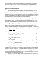
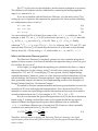
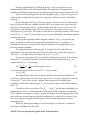
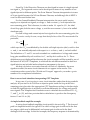
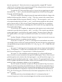
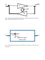
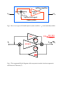
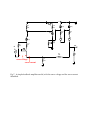
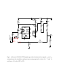
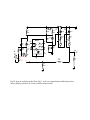
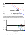
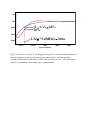
 http://www.ardem.com/free_downloads.asp v.1, 5/11/05 Methods of Design-Oriented Analysis
The GFT: A Final Solution for Feedback Systems
R. David Middlebrook
Are you an analog or mixed‐signal design engineer or a reliability engineer? Are you a manager, a design‐review committee member, or a systems integration engineer? Did you “fall off a cliff” when in your first job you discovered that the analysis methods you learned in college simply don’t work? There is help available. Design‐Oriented Analysis (D‐OA, don’t forget the hyphen!) is a paradigm based on the recognition that Design is the Reverse of Analysis, because the answer to the analysis is the starting point for design. Conventional loop or node analysis leads to a result in the form of a “high entropy expression” which is a ratio of sums of products of the circuit elements. The more loops or nodes, the greater the number of factors in each product. By common experience, we know that we will sink into algebraic paralysis beyond two or three loops or nodes. Such an analysis result is useless for design. In contrast, analysis results need to be derived in the form of “low entropy expressions” in which elements, such as impedances, are arranged in ratios and series‐
parallel combinations, and not multiplied out into sums of products. This is the most important principle of Design‐Oriented Analysis, whose objective is to enable a designer to work backwards from an analytic result and change element values in an informed manner in order to make the answer come out closer to the desired result (the Specification). Design‐Oriented Analysis is the only kind of analysis worth doing, since any other is a waste of time. There are many methods of D‐OA, some of them little more than shortcuts or tricks, but here the spotlight is on a new approach to analysis and design of feedback systems, based on the General Feedback Theorem (GFT). A typical analysis procedure followed by designers, and integration and reliability engineers, is to throw the whole circuit into a simulator and see what it does, possibly including attempts to measure the loop gain as well as external properties. The design phase may consist of little more than tweaking and sensitivity simulations. A much more efficient approach is to begin with a simple circuit in terms of device models absent capacitances and other parasitic effects, and then to add these sequentially. Even if you do little or no symbolic analysis, successive simulations tell you in what ways which elements affect the result, so that when you finally substitute your library process and device models you have a much better handle on where their effects originate. This procedure of “D‐OA by simulator” is significantly enhanced when the simulator incorporates the GFT, because the results for a feedback system are exact and not impaired by the approximations and assumptions inherent in the conventional single‐loop model. Moreover, it may no longer be necessary to attempt hardware measurements of loop gain, which in itself is a considerable saving of time and effort. What is the conventional approach? A
The well‐established method of analyzing a feedback system begins with the familiar block diagram of Fig. 1, from which the feedback ratio K and the loop gain T =A K are calculated. The designer’s job is to set K and the forward gain A so that the final closed‐loop gain H meets a specification, usually with the help of circuit simulator software. Several iterations, often aided by hardware measurements of the loop gain, may be needed before the closed‐loop gain meets the specification. Unfortunately, this approach can give incorrect results, stemming from the fact that the conventional block diagram of Fig. 1 is an incomplete representation of the actual hardware system. Your immediate reaction to this allegation may be: “If I’ve noticed any discrepancies between the predicted and the actual results, they’ve been small enough to neglect, or I’ve just ignored them anyway.” Wouldn’t it be better to be able to get the exact analysis results, quickly and easily, so that you could accurately predict the actual system performance? This desirable situation is now realized through use of the General Feedback Theorem (GFT). Let’s start by reviewing in more detail the conventional approach based on Fig. 1, for which the closed‐loop gain H (the “answer”) is given by A
A
=
(1) H=
1 + AK 1 + T
A “better” form is 1 AK
T
1
= H∞
= H∞
= H∞ D (2) H=
K 1 + AK
1+T
1 + T1
where 1
≡ ideal closed‐loop gain K
T ≡ AK ≡ loop gain H∞ ≡
(3) (4) It is convenient to define a discrepancy factor D as a unique function of T, T
1
D≡
≡
≡ discrepancy factor 1+T 1+ 1
T
(5) so that the closed‐loop gain H can be expressed concisely as (6) H = H∞ D Format (2) is “better” because H ∞ represents the specification, and is the only known quantity at the outset. So, K =1/ H ∞ is designed to meet the specification and the only hard part is designing the loop gain T so that the actual closed‐loop gain H meets the specification within the required tolerances. That is, the discrepancy factor D must be close enough to 1 over the specified bandwidth The form (2) or (6) is also “better” because it embodies one of the Principles of Design‐Oriented Analysis, namely “Get the quantities you want in the answer into the statement of the problem as early as possible.” In this case, H ∞ is the desired gain, and D is the discrepancy between H ∞ and the actual answer you’re going to get. Equally important, A is banished from the answer, because it contributes only via T , and its own value is of no interest. It is clear from the simple relation (5) that D is a unique function of T , which has several useful consequences. First, when T is large, D ≈ 1 which leads to the desired result that H ≈ H ∞ . Second, when T is small, D ≈ T and is small also, leading to a significant discrepancy between H ∞ and T . Third, where the magnitude of T falls to 1, the crossover frequency, marks the end of the frequency range over which T performs its useful function. How T crosses over determines the degree of peaking exhibited by D during its transition between 1 when T is large to T when T is small. According to (5), peaking in D is related to the phase margin of T , and translates by (6) directly to the closed‐loop response H. Thus, (5) and (6) expose the well‐known unique relationship between loop gain phase margin and both the frequency and time domain responses of the closed‐loop gain. What’s wrong with the conventional approach? The model of Fig. 1 is incomplete, because it does not account for bidirectional signal transmission in the boxes. In fact, the boxes are drawn as arrowheads on purpose to emphasize that reverse transmission is excluded. If both boxes have reverse transmission, there is also a nonzero reverse loop gain, and it is convenient to lump together all the properties omitted from this block diagram under the label nonidealities. Consequently, all analysis based on this model also ignores the nonidealities. In most textbooks and handbooks you can find whole sections that postulate a model in which each box of Fig. 1 is replaced by a two‐port model, thus retaining the bidirectionality of a real circuit. However, there are several disadvantages to this approach: (1) Four different sets of two‐port models are required to represent the four possible feedback configurations, shunt‐shunt, series‐shunt, etc., and in three of the four the model itself is still inaccurate because common‐mode gain is ignored; (2) Even though the nonidealities are incorporated in the model, how do you account for its effect upon the loop gain and the closed‐loop response? (3) Because the circuit elements are buried inside the two‐port parameters, which are themselves buried in expressions for the loop gain and closed‐loop gain, the results are high entropy expressions and are essentially useless for design. The Dissection Theorem is a completely general property of a linear system model The General Feedback Theorem (GFT) sweeps away all the a priori assumptions and approximations inherent in the above‐described conventional approach, and produces low entropy results directly in terms of the circuit elements. This is accomplished because the GFT does not start from a block diagram model, but is developed from a very basic property of a linear system, the Dissection Theorem. The Dissection Theorem says that any “first level” transfer function (TF) H of a linear system can be dissected into a combination of three “second level” transfer functions TF 1 , TF 2 , and TF 3 according to 1+ 1
H = TF1 TF1 3 (7) 1 + TF 2
These TF symbols are intentionally anonymous so that different physical significances can be assigned later. The second level TFs are calculated in terms of an injected test signal uz , as shown in Fig. 2. The injected test signal sets up ux going “forward” towards the output uo , and uy going “backward” towards the input ui , such that ux + uy = uz , in which ux , uy , uz may be all voltages or all currents, and ui and uo can independently be a voltage or a current. The second level TFs are defined by uy
uy
u
TF 2 ≡
TF 3 ≡
TF1 ≡ o
ui u = 0
ux u = 0
ux u = 0
y
i
o
(8) and the first level TF H is simply the output divided by the input (the “gain”) in the absence of the test signal: u
H≡ o
(9) ui u = 0
z
The definitions (8) require some interpretation. The TF 2 is the ratio of the signal going backward to the signal going forward from the test signal injection point, under the condition that the original input signal is zero. This is a “single injection” (si) calculation, the familiar method by which any TF is calculated. The TF 1 is the ratio of the output to the input when uy is nulled, a condition that is established by adjustment of the test signal uz so that its contribution to uy is exactly equal and opposite that from ui . This is a less familiar “null double injection” (ndi) calculation. Note that while H and TF 1 are both ratios of output to input, their values are different because, even if the input ui is the same, the uo for TF 1 contains a component due to uz that is absent in the uo for H. An ndi calculation is made after an ndi condition has been established, and is always easier and simpler than an si calculation. This is not an accident: any element in the system that supports a null signal might as well not be there, and so does not appear in the calculation or in the result. Also, you don’t have to know what the relation is between the two injected signals is; all you have to know is the equivalent information that the null exists. To emphasize this, consider the way to make the null self‐adjusting shown in Fig. 3: the imaginary infinite gain amplifier automatically nulls uy , and to calculate TF 1 from (8) you simply use the fact that uy is nulled, and you don’t have to know what uz is. The method of Fig. 3 can be implemented in a circuit simulator, since the “nulling amplifier” bandwidth is infinite even if its gain is not. The TF 3 in (8) is also an ndi calculation, and no further explanation is necessary. The (different) ndi condition can be established by connecting the nulling amplifier input to uo instead of to uy . If you’re not familiar with the Dissection Theorem, you can easily verify (7) by setting up a set of equations that represent the properties of a linear system containing two independent sources ui and uz : ux = Auo + Buz (10) uy = C ui + Duz (11) uz = ux + uy (12) You can evaluate the TFs of (8) and (9) in terms of the A, B, C, D coefficients. For example, to find TF 1 , set uy = 0 in (11) and solve for the ratio uz / ui = −C / D that nulls uy . In (10), ux = uz by virtue of uy = 0 in (12). Thus, uo = (1 − B) uz /A. Finally, substitute uz / ui = −C / D to get TF 1 = (B − 1)C/AD. Likewise, find TF 2 and TF 3 , and insert all three TFs into (7) to confirm that the result for H is the same as that obtained directly from (10) – (12) by setting uz = 0, which makes ux = −uy and H = −C / A . What is the Dissection Theorem good for? The Dissection Theorem is completely general, the only constraint being that it applies to linear systems. As with most theorems, the important thing is what is it good for, and how do you use it? At first sight, you might think that replacing one calculation by three is a step in the wrong direction. On the contrary, since (7) is itself a low entropy expression, the influences of TF 2 and TF 3 in modifying TF 1 are exposed, which is helpful design‐
oriented information. Moreover, since two of the three second level definitions of (8) are ndi calculations, the Dissection Theorem replaces a single complicated calculation by three potentially simpler calculations, thus implementing another of the Principles of Design‐Oriented Analysis, “Divide and Conquer.” Nevertheless, these are minimum benefits and much greater benefits accrue if the second level TFs have useful physical interpretations. Thus, the second level TFs (8) themselves contain the useful design‐oriented information and you may never need to actually substitute them into (7). For example, if TF 2 , TF 3 >> 1, H ≈ TF 1 . How do we determine the physical interpretations of (8)? In the above discussion based on Fig. 2, nothing was said about where in the system model the test signal is injected. Different test signal injection points define different sets of coefficients A, B, C, D and hence different sets of second level TFs. However, when a mutually consistent set is substituted into (7), the same H results: 1 + TF13b
1 + TF13a
H = TF1a
= TF1b
= ... (13) 1 + TF12 a
1 + TF12b
Therefore, the key decision in applying the Dissection Theorem is choosing a test signal injection point so that at least one of the second level TFs has the physical interpretation you want it to have. The Dissection Theorem can morph into the Extra Element Theorem (EET) For example, if the injection point is chosen so that uy goes into (voltage across, or current into) a single impedance Z , (7) becomes Z
1 + Zn
H = H Z =∞
Z
1 + Zd
(14) in which Zd , Zn are respectively the driving‐point impedance and the null driving‐
point impedance seen by Z , and H Z =∞ is the value of H when Z is infinite. In this form the Dissection Theorem becomes the Extra Element Theorem (EET), of which a useful special case is when Z is the only capacitance in an otherwise resistive circuit. Then, H Z =∞ is the first level TF (the “gain”) when the capacitance C is absent (zero), and the pole and zero are exposed directly as 1/ CRd and 1/ CRn . The EET will not be further discussed here, because the spotlight is on another example of the choice of injection point. The Dissection Theorem can morph into the General Feedback Theorem (GFT) It is easy to see that the block diagram of Fig. 4 represents (7), and is immediately recognizable as an augmented version of the conventional feedback block diagram of Fig. 1, which represents (2). So, where does the test signal have to be injected so that TF 1 has the physical interpretation of H ∞ ? The answer is obvious: Since H ∞ is H when the error signal vanishes (infinite loop gain), and TF 1 is H when uy is nulled, then uz must be injected at the error summing point so that uy represents the error signal. At the same time, this makes TF 2 have the physical interpretation of the loop gain T , since the test signal injection point is inside the loop. Finally TF 3 , which does not have a corresponding appearance in Fig. 1, is a new TF that can be designated Tn , since by (8) it is defined as a loop gain with uo nulled. Following the above procedure, (7) becomes 1 + T1
n
H = H∞
1 + T1
(15) and in this form the Dissection Theorem becomes the General Feedback Theorem. For the second level TFs to have the desired physical interpretations TF 1 = H ∞ , TF 2 = T , TF 3 = Tn , the test signal uz must be inside the loop and at the error summing point, as illustrated in Fig. 5. Equations (8) then become uy
uy
u
T ≡
Tn ≡
H∞ ≡ o
ui u = 0
ux u = 0
ux u = 0
y
i
(16) o
With H ∞ , T , and Tn calculated from (16), the result (15) is represented by the “augmented” block diagram of Fig. 6. Because superficially Fig. 6 differs from Fig. 1 only in the presence of an additional block that contains the nonidealities, it is important to emphasize the fundamental difference between the conventional approach and that based on the GFT. In the conventional approach, the block diagram of Fig. 1 is the starting point, in which reverse transmission in both boxes is ignored, and the result (2) is developed from Fig. 1. In the GFT approach, Fig. 5 is the starting point, and the result (15) is developed from (16) directly from the complete circuit without any assumptions or approximations. Since (15) is represented by Fig. 6, the block diagram of Fig. 6 is part of the result. The boxes in Fig. 6 are unidirectional, and do not necessarily correspond to any separately identifiable parts of the circuit. The values of these boxes, expressed in terms of the second level TFs H ∞ , T , and Tn , automatically incorporate any nonidealities that may be present in the actual circuit. Although the augmented block diagram exhibits a “loop,” it represents any linear system even if there is not a physically discernible loop. An example is a Darlington Follower, for which the GFT affords a means of investigating the well‐
known potential instability. It is apparent that the null loop gain Tn contains the first‐order effects of nonidealities, although there may also be second‐order effects upon the loop gain T . Thus, the T in (2) may not be the same as the correct T in (15). Since it was convenient in (5) to introduce the discrepancy factor D as a unique function of T , it is likewise useful to introduce the null discrepancy factor Dn as a unique function of Tn , according to 1 + Tn
1
Dn ≡
≡ 1+
≡ null discrepancy factor Tn
Tn
(17) so that the final result for the first level TF T can be written H = H∞ DDn (18) The importance of this result is that the familiar tenet must be modified: the closed‐loop frequency domain and time domain responses are no longer uniquely determined by the loop gain T and its phase margin. Instead, these responses are modified by a noninfinite value of the null loop gain Tn via a nonunity value of the null discrepancy factor Dn . Calculation of the second level TFs H ∞ , T , and Tn can be done symbolically, or numerically by use of a circuit simulator. The Intusoft ICAP/4 simulator incorporates GFT Templates that apply a voltage or current test signal, set up the appropriate si and ndi conditions, and perform the required calculations. As a user, all you have to do is choose the proper test signal injection point, which is inside the loop at the error summing point. However, before proceeding to a circuit example, it is necessary to make an extension of the Dissection Theorem. The GFT for two injected test signals is the “Final Solution” From Fig. 2, the Dissection Theorem was developed in terms of a single injected test signal uz , but a general version can be developed in terms of any number of test signals injected at different points. The Extra Element Theorem interpretation in terms of N test signals becomes the N Extra Element Theorem, and although this is NEET it won’t be discussed further here. For the General Feedback Theorem interpretation, the most useful version employs two injected test signals, a voltage e z and a current jz , both injected at the error summing point. This is because, in order to make H ∞ equal to 1/ K , the ideal closed‐loop gain, both the error voltage vy and the error current i y have to be nulled simultaneously. For dual voltage and current injected test signals at the error summing point, the GFT of (7) remains exactly the same, except that the definitions of the TFs are extended. In particular, u
H∞ ≡ o
(19) ui v ,i = 0
y y
which says that H ∞ is established by the double null triple injection (dnti) condition that e z and jz are mutually adjusted with respect to ui so that vy and iy are both nulled. The definitions of T and Tn are each extended to a combination of voltage and current loop gains established by ndi conditions for T , and by dnti conditions for Tn . These definitions are not displayed here because the circuit examples will be treated by use of the Intusoft ICAP/4 GFT Templates, in which all the calculations needed for dual test signal injection are included and are therefore transparent to the user. Are dnti calculations even easier than ndi calculations? Absolutely: the more signals are nulled, the more circuit elements do not appear in the answer. This constitutes another round of the “Divide and Conquer” approach: you make a greater number of less complicated calculations. How to use a circuit simulator incorporating GFT Templates In any case, if you’re going to use a circuit simulator rather than doing symbolic analysis, all you need to do is choose an injection point inside the loop at the error summing point, plus select the appropriate GFT Template according to whether single or dual test signal injection is required to null simultaneously the voltage and current error signals. The Template does simulation runs to calculate the second level TFs H ∞ , T , and Tn in (15), and does post‐simulation calculations to produce the discrepancy factors D and Dn in (18). A simple feedback amplifier example A series‐shunt feedback amplifier circuit model is shown in Fig. 7. The forward path is a simplified model of a typical IC in which voltage gain is achieved in the first two stages, which may be differential, and current gain is achieved in the final darlington follower stage. In this first example, the frequency response is determined by the sole capacitance Cc . Each active device is represented by a simple BJT T‐model, which has the advantage of also representing an FET by setting the drain current equal to the source current, as is done in this example. To apply the GFT, the crucial first step is to choose the test signal injection point that makes H ∞ , T , and Tn have the desired interpretations of ideal closed‐loop gain, loop gain, and null loop gain. The error voltage is the voltage between the input and the fed back voltage at the feedback divider tap point, labeled vy in Fig. 7. The error current is the current drawn from the feedback divider tap point, labeled iy in Fig. 7. The test signals e z and jz are to be injected inside the loop so that vx and ix are the driving signals for the forward path, as shown in Fig. 8. Thus, the test signal configuration meets the two conditions that injection occurs at the error summing point, and is inside the loop, implementing the general model of Fig. 5. To invoke the GFT Template, the appropriate dual‐injection icon is selected and connected to provide the test signals e z and jz , as in Fig. 9. The icon also provides the system input signal ei and observes the output signal vo , because it has to adjust the test signals relative to the input to establish various nulls, one of which is the output signal. Another Principle of Design‐Oriented Analysis is “Figure out as much as you can about the answer before you plunge into the analysis.” In this case, we expect H ∞ to be 1/ K , the reciprocal of the feedback ratio which was initially chosen to meet the system specification, because the injection configuration was specifically set up to achieve this. Here, 1 / K = ( R1 + R2) / R1 = 10 ⇒ 20dB, flat at all frequencies. We expect T to be large at low frequencies and to have a single pole determined by Cc . Consequently, D will be flat at essentially 0dB at low frequencies, with a pole at the crossover frequency of T , beyond which D will be the same as T . We expect Tn to be noninfinite, and consequently Dn to be not 0dB, because there is nonzero reverse transmission through the feedback path. That is, if the forward path through the active devices dies, the input signal ei can still reach the output vo by going through the feedback path in the “wrong” direction. The principal benefit of the GFT is to permit calculation of this effect, which is not accounted for in the conventional model, in order to determine whether or not it is significant. The GFT results for the three second level TFs for the model of Fig. 9 are shown in Fig. 10, and the expectations are indeed borne out. The results are repeated in Fig. 11 with the loop gains replaced by their corresponding discrepancy factors, both of which are essentially 0dB at low frequencies. Also shown is the final result for the first level TF H , the closed‐loop gain, which from (18) is the direct superposition of the H ∞ , D , and Dn graphs. This final result shows that the bandwidth of H is determined by the T crossover frequency as in the conventional approach, and that reverse transmission (“wrong way”) through the feedback path does not have any significant effect until the much‐higher null loop gain crossover frequency. A more realistic feedback amplifier model The more interesting model of Fig. 12 includes two added capacitances for each active device. This is a much more realistic model, and of course library device models can be substituted. What are our expectations for the results in comparison with those for Fig. 9? Since all the extra elements are capacitances, we expect the low frequency properties to remain the same, but the dominant pole and hence the loop gain crossover frequency would be lowered. Therefore, to enable a more meaningful comparison between the two circuits, Cc in Fig. 12 has been reduced sufficiently to preserve the same loop gain crossover frequency. Nevertheless, the extra capacitances create more poles and zeros, so the high frequency loop gain is expected to be more complicated. The major consequence of the presence of the extra capacitances is that there is now a second feedforward path (through a string of capacitances), in addition to that through the feedback path in the “wrong” direction, through which the input signal can reach the output; also, there is now nonzero reverse transmission through the forward path, which in turn creates a nonzero reverse loop gain. It is not necessary to separate these nonidealities, because they are all automatically accounted for in the calculation of the loop gain (usually little effect) and in the null loop gain (the major effect). The quantitative results of the GFT Template simulations for Fig. 12 shown in Figs. 13 and 14 bear out the expectations. The null loop gain crossover frequency is drastically lowered, and even though the magnitude of the null discrepancy factor Dn is 0dB at both ends of the frequency range, its phase undergoes a huge lag that is transferred directly into a correspondingly huge phase lag in the final closed‐loop gain H . Although the magnitude of H at high frequencies may not be of much interest in the frequency domain, its corresponding phase has a controlling effect in the time domain. The step responses of the circuits of Fig. 9 and Fig. 12 are shown in Fig. 15. The huge phase lag of H at high frequencies for the circuit of Fig. 12 causes the expected delay in the step response; however, the ensuing rise time is shorter than for Fig. 9, with the perhaps unexpected beneficial result that the final value is achieved sooner for Fig. 12 than for Fig. 9. The bottom line is that the GFT of (28), whose principal difference from (6) of the conventional approach is the presence of the null discrepancy factor Dn , predicts a substantial modification of the closed‐loop performance H . The nonidealities represented by Tn or Dn are always present in a realistic model of an electronic feedback system, and in at least some respects, can actually improve rather than degrade the performance. This rare exception to Murphy’s Law provides added incentive to utilize the GFT. A method of finding loop gain from a voltage loop gain Tv and a current loop gain Ti calculated successively from single voltage and current injected test signals has been quite widely adopted since it was proposed in 1975. The formula is T T −1
1
1
1
or T = v i
=
+
1 + T 1 + Tv 1 + Ti
2 + Tv + Ti
(20) However, this formula was based on the conventional block diagram of Fig. 1, and does not account for nonzero reverse loop gain. You no longer need to measure loop gain directly In the conventional approach, efforts are often made to measure loop gain on the actual hardware in order to check that the phase margin is adequate, although little or no thought is given to whether or not the measurement is consistent with the actual closed‐loop gain. It is very awkward to inject even a single test signal into an IC, and dual or triple injection to set up ndi or dnti conditions is so burdensome that it is rarely attempted. Fortunately, it is no longer necessary to measure loop gain directly. The GFT of (18) is exact with respect to the simulated model, and all you have to do is measure the final closed‐loop TF H , which you would do anyway to check whether it meets the specification. If the simulated H differs from the measured H , you have to adjust the model until the two are the same. When this is achieved, you know the model is correct and then the simulation tells you what T and Tn are individually. This is the culmination of the D‐OA process. More useful techniques for analog engineers The GFT is completely general, the only requirement being that it applies to a linear system model. The symbol H has been used here for the first level TF purposely to avoid the connotation of “gain,” because it could equally well represent input or output impedance, power supply rejection, or indeed any transfer function of interest. It was mentioned above that the EET interpretation of the Dissection Theorem can be extended to any number of injected test signals, leading to the NEET Theorem. The GFT interpretation could likewise be extended, in particular to two pairs of injected voltage and current test signals, which would open the door to analysis of feedback amplifiers containing both differential and common mode loops. Analog, mixed‐signal, and power supply design engineers are not the only ones to benefit from an ability to apply the powerful methods of Design‐Oriented Analysis. Those who review and verify designs of others also need to know how design‐oriented results of analysis should be presented. Therefore, managers, system integration engineers and reliability engineers who evaluate the products of other companies as well as their own, also can significantly increase their effectiveness by applying the methods of D‐OA. Then, if you hold any of the above job titles, you can contribute meaningfully to design review discussions, instead of just saying to the presenting designer “Well, it looks as though it’s coming along all right; carry on!” In fact, you can improve the effectiveness of the whole project by requiring that design engineers present their results according to the Principles of Design‐Oriented Analysis. For further information on the GFT, EET, and Design‐Oriented Analysis in general, see http://www.rdmiddlebrook.com. For further information on the Intusoft ICAP/4 Circuit Simulator, including a GFT Template User’s Manual, see http://www.intusoft .com. ui
uo = Hui
A
+ -
T = AK
K
Fig.1. The familiar single‐loop block diagram of a feedback system. The arrow‐head shapes imply that the signal goes only one way. ui
< uy
> ux
uz
uo
injected test signal
linear system
Fig.2. General model of a linear system with input ui and output uo , and an injected test signal uz . nulling amplifier
ui
< uy
infinite
gain
> ux
uz
uo
injected test signal
linear system
Fig.3. How to set up a null double injection (ndi) condition: uy is automatically nulled. TF 4 ≡
TF 4
TF 3
ui
+
−
+
TF 1TF 2
+
TF 1 TF 2
TF 3
uo = Hui
TF 2
1
TF 1
Fig.4. This augmented block diagram with anonymous transfer functions represents the Dissection Theorem (7). ui
ux
uy
+
<
−
Note boxes,
<
uo = Hui
<
uz
not
arrowheads
Fig.5. When the test signal is injected inside the loop at the error summing point, the Dissection Theorem of (7) becomes the General Feedback Theorem (15). H0 ≡
H0
Tn
ui
+
−
+
H ∞T
+
H ∞T
Tn
uo = Hui
T
1
H∞
Fig.6. This block diagram for the General Feedback Theorem is a morphed version of Fig. 4, in which Tn (or H0 ) represents the main effects of the nonidealities. V2
R3
200
rm2
200
i(V2)
V3
i(V1)
ui
i(V4)
rm3
50
rm4
10
V4
Cc
R8
20p
10meg
rm1
50
Rs
100
i(V3)
uo
V1
+
−
R2
900
>
error voltage
RL
1k
R1
100
error current
Fig.7. A simple feedback amplifier model, with the error voltage and the error current identified. V2
R
200
rm
200
i(V2
V3
i(V1
rm
50
R
100
u
R
10me
i(V3
i(V4
rm
50
rm
10
V4
C
20p
u
V1
ix
X
− vx < +
W
+ vy
−
>
Y iy
R
900
R
1
R
100
Fig.8. The crucial step: Choose the test signal injection point inside the loop so that vy is the error voltage and iy is the error current. V2
R3
200
rm2
200
i(V2)
GFTv
ui
rm1
50
Rs
100
ui
V1
ix
X
− vx < +
W
+ vy
−
V3
+
Ui - Ei Vo Uo
-
Y Iy
-+
- Ez
Vy
+
W
i(V4)
rm3
50
rm4
10
uo
+
i(V1)
i(V3)
Ix
Cc
R8
20p
10meg
X
+
Vx
Jz -
V4
uo
xgft
GFTv
R2
900
>
Y iy
RL
1k
R1
100
Fig.9. An Intusoft ICAP/4 GFT Template provides the injected test signals e z and jz , and performs the simulations and post‐processing required to obtain H ∞ , T , and Tn , and hence H , for the GFT of (15). dB
80.0
40.0
H∞
0
-40.0
-80.0
100m
Tn
T crossover 5.4MHz T
Tn crossover 7.9GHz
10
1k
100k
10Meg
frequency in hertz
1G
100
Fig.10. The expectations are borne out: H ∞ is flat at 20dB, and T has a single pole. The null loop gain Tn is not infinite, because of nonzero reverse transmission through the feedback path (a feedforward path). dB
80.0
40.0
H∞
Dn
0
H = H ∞ DDn
-40.0
D
-80.0
100m
10
1k
100k
10Meg
frequency in hertz
1G
100
Fig.11. T and Tn replaced by their corresponding discrepancy factors D = T /(1 + T ) and Dn = (1 + Tn ) / Tn . The normal closed‐loop gain H = H ∞ D Dn differs from H ∞ not only because of D , but also because of Dn , although this effect is small. V2
C2d
16p
R3
200
C3t
5p
C4t
50p
rm2
200
i(V2)
GFTv
ui
Rs
100
ui
C1d
30p
rm1
50
V1
−
V3
Ui - Ei Vo Uo
+
i(V1)
+ vy
C3d
30p
uo
+
Ct1
5p
ix
X
− vx < +
W
Ct2
5p
-
Y Iy
-+
- Ez
Vy
+
W
Ix
i(V4)
rm3
50
rm4
10
C4d
160p
V4
Cc
R8
5p
10meg
X
+
Vx
Jz -
i(V3)
uo
xgft
GFTv
R2
900
>
RL
1k
Y iy
R1
100
Fig.12. A more realistic model than Fig. 7, with two capacitances added per active device (library models of course could be substituted). dB
80.0
40.0
H∞
0
Tn
T
T crossover 5.4MHz
-40.0
Tn crossover 82MHz
-80.0
100m
10
1k
100k
10Meg
frequency in hertz
2
100
1G
Fig.13. There is now an additional feedforward path, nonzero reverse transmission through the forward path, and nonzero reverse loop gain, causing the null loop gain crossover frequency to be much lower. 360
180
0
-180
-360
hdbinf, ddb, ddbn, hdb in unknown
deg dB
80.0
40.0
Dn
0
H∞
H = H ∞ DDn
-40.0
H
D
-80.0
100m
10
1k
100k
10Meg
frequency in hertz
1G
Fig.14. The extra capacitances cause the null discrepancy factor Dn to be drastically different, resulting in a huge phase lag of 450o in the normal closed‐loop gain H . 2
100
1.40
1.00
(1 − 1 / e) = 64%
50%
600m
200m
1 /(2π * 5.4MHz) = 30ns
-200m
20.0n
60.0n
100n
time in seconds
140n
180n
Fig.15. For the circuit of Fig. 12, the huge phase lag of H causes the expected delay in the step response; however, the ensuing rise time is shorter, with the perhaps unexpected beneficial result that the final value is achieved sooner. At least in some respects, nonidealities can actually improve performance!