1
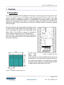
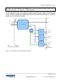
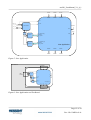
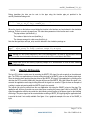
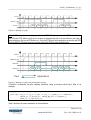
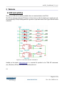
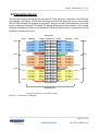
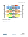
aes220 User Manual HighSpeed USB FPGA MiniModule Aessent Technology Ltd aes220 HighSpeed USB FPGA MiniModule User Manual Version 1.4.1 Doc Nb: UM22001A www.aessent.com MiniModule Series User Manual aes220_UserManual_V1_4_1 Change History Version Changes Author V1.2 Original Version Sébastien Saury V1.4 Update pipes interface (introduction of PAUSE_in input) Sébastien Saury V1.4.1 Added note to clarify pipe direction convention and diagram of test bench Sébastien Saury overview Doc. Nb: UM220-01-A aes220_UserManual_V1_4_1 Table of Contents 1 Overview..........................................................................................................................................5 1.1 Description................................................................................................................................5 1.2 Block Diagram..........................................................................................................................7 2 Operation..........................................................................................................................................8 2.1 Note to the user.........................................................................................................................8 2.2 Power Supplies.........................................................................................................................8 2.3 Start-Up and Shut-Down..........................................................................................................9 2.4 Reset..........................................................................................................................................9 2.5 Sleep Mode...............................................................................................................................9 2.6 Programming the FPGA and Micro-controller.........................................................................9 2.7 Communicating with the PC...................................................................................................10 2.7.1 Overview.........................................................................................................................10 2.7.2 FX2 Interface..................................................................................................................13 2.7.3 Logical OR......................................................................................................................14 2.7.4 PipeIn: receiving data......................................................................................................15 2.7.5 PipeOut: Writing data......................................................................................................17 3 Features...........................................................................................................................................21 3.1 LED and switches...................................................................................................................21 3.3 I2C..........................................................................................................................................22 3.4 Connectors pin-out..................................................................................................................23 3.5 Stack-up format.......................................................................................................................25 4 Characteristics................................................................................................................................26 4.1 FPGA Power Dissipation........................................................................................................26 4.1.1 FPGA Thermal Characteristics.......................................................................................26 4.1.2 FPGA Power Limits........................................................................................................26 4.2 Board Dimensions...................................................................................................................29 Doc. Nb: UM220-01-A aes220_UserManual_V1_4_1 Illustration Index Figure 1: Module Top View..................................................................................................................5 Figure 2: Daughter Boards Stack Up....................................................................................................5 Figure 3: aes220 Block Diagram..........................................................................................................7 Figure 4: FX2 Interface and Pipes Block Diagram.;..........................................................................11 Figure 5: User Application.................................................................................................................12 Figure 6: User Application and Test Bench........................................................................................12 Figure 7: Reading from a pipe............................................................................................................15 Figure 8: Writing to a pipe..................................................................................................................18 Figure 9: Writing to a pipe and pausing the transfer..........................................................................18 Figure 10: LED and switches schematics...........................................................................................21 Figure 11: Connector P1 Mapping.....................................................................................................23 Figure 12: Connector P2 Mapping.....................................................................................................24 Figure 13: Daughter Boards Stack-Up...............................................................................................25 Figure 14: Max Recommended Power...............................................................................................27 Figure 15: Absolute Maximum Power...............................................................................................28 Figure 16: aes220 Board Dimensions.................................................................................................29 Index of Tables Table 1: Power Supply Capabilities......................................................................................................8 Table 2: aes220_FX2_Interface Parameters.......................................................................................14 Table 3: aes220_PipeIn Parameters....................................................................................................16 Table 4: aes220_PipeOut Parameters.................................................................................................19 Table 5: FPGA Thermal Characteristics.............................................................................................26 Table 6: Max Recommenced Power...................................................................................................27 Table 7: Absolute Maximum Power...................................................................................................28 Doc. Nb: UM220-01-A aes220_UserManual_V1_4_1 1 Overview 1.1Description The aes220 is a highspeed USB 2.0 (480Mb/s) FPGA module for rapid prototyping and incorporation in other systems. It combines a Cypress CYC7C68013A FX2LP HighSpeed USB 2.0 microcontroller with a Xilinx Spartan 3AN device (XC3S200AN) connected to a 128Mb SDRAM. The module includes its own DC/DC converter and crystal oscillator. All it requires is a 5Vdc power supply if disconnected from the USB. Its tiny 43x61mm size allows fitting in confined spaces and thanks to its stackable interface it can easily be combined with other modules. The device small size does not prevent it from offering a total of 72 General Purpose Inputs Outputs (GPIO) 12 of which can be used as clock inputs fed directly to the FPGA Global Clocks Buffers (GCLK). The 36 GPIO on connector P1, including the clocks, can be used single ended or as 18 differential pairs. The two 48 pin 0.1” pitch through hole connectors footprints on either side of the module allow for it to be stacked up either on top, bottom or both sides. To add to the Figure 1: Module Top View flexible GPIO scheme power and grounds pins are spread symmetrically among the two main connectors. This feature allows for modules a third of its size to be directly interfaced to the aes220. Each slot hence connecting to power supply pins and interfacing with 24 GPIO, 4 of which usable as clock signals to the FPGA. Figure 2: Daughter Boards Stack Up Page 5 of 29 Doc. Nb: UM220-01-A aes220_UserManual_V1_4_1 The module offers a flexible clock implementation with the microcontroller clock connected to the FPGA and 16 GCLK inputs present on the external connectors allowing for multiple clock inputs (for a 10MHz external reference for example, but also for running buses or serial links requiring an external clock). The FPGA possesses four Digital Frequency Synthesiser (DFS) to multiply any clock provided up to 334MHz. Thanks to the FPGA 4Mb of internal Flash memory no external device is required for the FPGA to keep its configuration over power cycles. The integrated flash memory can be used for device configuration, with enough space for two different configurations, or data storage or a mix of both. In addition the SDRAM device provides 128Mb of RAM memory with fast access time (16bits parallel data bus and 100MHz clock). See the Xilinx web site for more documentation on the FPGA itself. The Cypress FX2LP microcontroller provides the communication between the host computer and the FPGA. The RAM and EEPROM of the microcontroller are fully accessible allowing customisation of the communication link. However the communication channel between the PC, microcontroller and FPGA is fully setup requiring no intervention from the user. Both the microcontroller and the FPGA can be configured using a simple USB cable (or also using a JTAG programmer via standard Xilinx JTAG connector in the case of the FPGA). VHDL or Verilog code synthesising for the FPGA is via Xilinx free ISE WebPACK or ISE Design Suite both downloadable from the Xilinx website. There is no need for learning about USB communication protocols as libraries are provided for dealing with the communication between the host PC, the microcontroller and the FPGA. All programs and libraries are free and Open Source so as not to be tied up with any proprietary tools and permitting customisation if required. Examples, tools and libraries are all available on both Windows and Linux platforms. Page 6 of 29 Doc. Nb: UM220-01-A aes220_UserManual_V1_4_1 1.2Block Diagram aes220 Connector 1, banks A to C x1 (uC) 36 GPIOs Ext. Wake Up Clock Cypress FX2 uC x1 (uC reset) 22 GPIOs + GPIF signals I2C EEPROM 128Kb PSU 4.5 to 5.5V in 1.2/1.8/3.3V out x4 (User Spec.) Bank3 3.3V x1 (Done Pin) FPGA Xilinx Spartan3AN XC3S200AN JTAG Bank0 3.3V Connector Clock Bank2 3.3V USB Bank1 1.8V SDRAM 128Mb 36 GPIOs or 18 Diff. Pairs x2 (User Specifics) Connector 2, banks D to F Figure 3: aes220 Block Diagram Page 7 of 29 Doc. Nb: UM220-01-A aes220_UserManual_V1_4_1 2 Operation 2.1Note to the user The operation described in this chapter are for the software, firmware and VHDL code provided with the module. As these are open source and freely modifiable by the user some part of this manual could stop being relevant and the onus would be on the user to document its own work. The code and compiled modules required to set the module in its original condition are available on the website at www.aessent.com . 2.2Power Supplies The module can be powered up directly from the USB power supply or from an external 4.5 to 5.5V supply provided via one or more of the six Vin pins available on the two main connectors P1 and P2. The two power supply paths (i.e. USB and external supply paths) can be swapped from one to the other without disrupting the functioning of the module. When an external supply is detected the supply from the USB port is turned off. By specification a USB 2.0 host can provide up to 500mA of current (1A if using a double connector cable). As depending on the application a module can draw more than that it is the responsibility of the user to ensure its application won't exceed the USB specification (using Xilinx power estimator tools for example). If it is the case a 5V external power supply via P1 or P2 must be used. The onboard power supply converter can provide up to 1.5A on the 3.3V rail used by the inputs/outputs of the FPGA. On the unlikely event that more power is required it is possible to turn off the onboard power supply and provide the 3.3V directly to the FPGA, please refer to the API on how to turn off the 3.3V rail. Note, however, that for this amount of power the FPGA will require some form of cooling to be provided. See table 1 below for the different supplies capabilities. Note: it might also be necessary to turn of the 3.3V rail if stacking up boards together. Only one of the boards should provide the 3.3V to the rail (or none if an external 3.3V power supply is used). Power Supply Capability Demand Client Device Switching 3.3V 1.5A Design dependent* (max 4A!) FPGA I/O Bank 0,2,3 Switching 1.2V 1.5A Design dependent* (max 600mA) FPGA Core Linear 3.3V 300mA Design dependent* (max 150mA FPGA + 85mA FPGA Aux, microcontroller uC) Linear 1.8V 300mA 70mA SDRAM + FPGA Bank 1 activity SDRAM, FPGA Bank 1 I/O Table 1: Power Supply Capabilities * Power dissipation will limit how much current can be drawn to something lower than the power supply limits. Page 8 of 29 Doc. Nb: UM220-01-A aes220_UserManual_V1_4_1 2.3StartUp and ShutDown The module powers up automatically when any of the power supply is present. No special step is required. The microcontroller will wake up first and only then allow the FPGA to configure from its internal flash (if programmed). Shuttingdown the module is a matter of cutting off the power supplies to it. 2.4Reset There are two ways of resetting the module: via a USB command or by pressing the reset switch on the board. See the API documentation on how to perform an USB reset. The reset, whether software via USB or hardware via the reset switch, resets the microcontroller which in turns resets the FPGA. 2.5Sleep Mode Both the microcontroller and FPGA can be put into lowpower mode independently of each other. The micro controller commands the SUSPEND pin of the FPGA. An API function is used to send the relevant command to the microcontroller. Note however that to wake up the microcontroller the W.UP pin on the board has to be pulled low as USB communication is lost when the microcontroller is in lowpower mode. 2.6Programming the FPGA and Microcontroller Programming both the FPGA and the microcontroller of the aes220 has been made very simple thanks to the aes220 Programmer. It is a GUI based software that makes use of the functions present in the API to program both circuits. The microcontroller does not require to be programmed as it can be used directly with already loaded firmware. However it is worth keeping an eye for new versions of the firmware published on the website (www.aessent.com). When programming the microcontroller it is possible to either overwrite the program present in the RAM of device or in the EEPROM. If loaded into the RAM the program will revert to the original firmware (or whatever firmware is present at that time in the EEPROM) on a reset or power cycle. If loaded into the EEPROM the program become permanent. Note that if the program loaded in the EEPROM is faulty or does not set the USB communication properly then there is the possibility to “brick” the device. That is the device looses USB communication and hence cannot be reprogrammed. However there is a simple solution to this which is to remove the cap on jumper one and reset or power cycle the device. See the chapter on recovering from a wronglyprogrammed EEPROM in the installation manual pertaining to your operating system. Most Xilinx FPGA do not have intrinsic memory and need to be configured on or after powerup. The device used on the aes220 however incorporates some Flash memory that can be programmed with the FPGA configuration file. At power on the FPGA will automatically fetch this configuration file from the memory and Page 9 of 29 Doc. Nb: UM220-01-A aes220_UserManual_V1_4_1 boot up from it. There is no particular requirement from the configuration file in order to achieve this. The boot up process is handled by the microcontroller. It is not a requirement to program the Flash memory. The device can also be configured and simply run from this configuration until it is powered off or reset at which point the configuration will be lost. 2.7Communicating with the PC Communicating between a FPGA and a PC via a USB link can be a tricky matter. However thanks to the API and VHDL interface provided it needs not be. The microcontroller which handles the whole USB communication channel is programmed in such a way as to create a simple yet versatile interface between the FPGA and the PC. No indepth knowledge of USB communication is required to transfer data back and forth between the two. The interface allows highspeed data channels between the PC and the FPGA as well as six user general purpose pins which can be used for example as control or status pins for the user application if required. 2.7.1 Overview A USB communication channel is usually called a pipe. On the PC side sending data out from the PC to the FPGA will be done using the function pipe_Out() and receiving data from the FPGA will be done via the function pipe_In(). The exact syntax for both functions is described in the API documentation but each function requires a buffer of 8 bit unsigned integers, the size of the buffer and a pipe address. Note: in a USB communication the host is the PC and is the master. There is no interrupt process for the slave to signal to the master it wants to communicate. The host decides when to send and receive data (using pipe_Out and pipe_In functions in this case) as well as how much data is transferred. On the microcontroller side the data sent by the PC or about to be sent to the PC is stored into dedicated FIFO memories. The FPGA interface provided handles the FIFO communication simplifying further the communication with the PC. The interface is constituted of a main interface module (FX2_Interface) and as many as 128 pipes, although in practice much fewer will be required. Each pipe offers an 8 bit wide data bus with read/write control signals as well as a pause signal so the user application can pause the transaction if required. The user instantiates as many pipes as required in its application and gives them all a unique address. This is depicted in figure 4 below. Two sort of pipes are provided, PipeIn and PipeOut. PipeIn is used when receiving data into the FPGA and PipeOut when sending data to the host PC. Note: on the FPGA side the pipeIn_ent entity is used to receive data from the PC and the pipeOut_ent entity to send data to the PC. So pipe_out() function of the PC connects to the pipeIn_ent entity of the FPGA and pipe_in() function of the PC connects to pipeOut_ent entity of the FPGA. The in/out direction is always the one relating to the device being programmed (PC or aes220). Keep in mind however that the simulation functions provided to write test benches, although written in vhdl Page 10 of 29 Doc. Nb: UM220-01-A aes220_UserManual_V1_4_1 and used in the ISE environment, are emulating the PC side of the chain and hence adhere to the PC convention (in is FPGA → PC, out is PC → FPGA). See below. To simplify the simulation two functions PipeIn and PipeOut are available in the Simulation package provided. The user application can hence be developed and simulated using the signals coming in and out of the pipes and does not have to contend with the handling of the FX2 microcontroller FIFOs. See Figures 4, 5 and 6 for a graphical overview of the different modules. RST RST_in IFCLK FI_in IF_out FX2 Interface FI_io IP PI OR READ_RQ PipeIn 1 PAUSE DATA READ_RQ PipeIn 2 PAUSE DATA WRITE_RQ PipeOut1 PAUSE DATA FX2 Connections FPGA Interface FPGA Application Figure 4: FX2 Interface and Pipes Block Diagram.; Page 11 of 29 Doc. Nb: UM220-01-A aes220_UserManual_V1_4_1 BANKA BANKB BANKA BANKB BANKC BANKC RST RST_in IFCLK FI_in Switches FX2 Interface IF_out FI_io SW PI IP LEDs OR PipeIn 1 P1_READ_RQ PAUSE P1_DATA PipeOut 2 P2_WRITE_RQ PAUSE AP2_DATA LED User Application BANKD BANKE BANKD BANKE BANKF BANKF Figure 5: User Application Test Bench I/O Banks BANKA BANKB BANKC BANKA BANKB BANKC RST RST_in USB Comms FI_in IF_out IFCLK Switches FX2 Interface FI_io SW PI IP LEDs OR PipeIn 1 P1_READ_RQ PAUSE P1_DATA PipeOut 2 P2_WRITE_RQ PAUSE AP2_DATA LED User Application BANKD BANKE BANKF BANKD BANKE BANKF I/O Banks Figure 6: User Application and Test Bench Page 12 of 29 Doc. Nb: UM220-01-A aes220_UserManual_V1_4_1 2.7.2 FX2 Interface The microcontroller deals with all the USB communications and offers a simplified FIFO interface directly connected to the FPGA. The FX2_Interface joins this interface to the various pipes used in the application. Only one FX2_Interface should be instantiated in the application and all pipes linked to it. The FX2_interface should be instantiated and mapped as follow: fx2_Interface : aes220_FX2_Interface_ent port map (RST_in => RST_in, ifCLK_out => ifClk_s, User app FI_in => FI_in, IF_out => IF_out, FI_io => FI_io, PI_in => pi_s, IP_out => ip_s); Table 3 describes the various parameters of the instantiation. Page 13 of 29 Doc. Nb: UM220-01-A aes220_UserManual_V1_4_1 Instantiation Parameters Parameters Description fx2_interface : aes220_FX2_Interface_ent fx2_interface is an instance of the aes_220_FX2_Interface_ent component (the only one FX2 Interface to be instantiated). RST_in => RST_in Reset signal coming from the microcontroller (or the host PC). Mapped straight to the top level port of the application. The port is defined in the aes220_RevA1_FX2_Interface.ucf constraint file. IFCLK_out => ifclk_s The 48MHz clock coming from the microcontroller and transiting via the FX2 Interface. This is the clock signal to use with the rest of the application when dealing with the pipes. FI_in => FI_in Signal bus going from the FX2 to the FX2 Interface. Mapped straight to the top level port of the application. The port is defined in the aes220_RevA1_FX2_Interface.ucf constraint file. IF_out => IF_out Signal bus going from the FX2 Interface to the FX2. Mapped straight to the top level port of the application. The port is defined in the aes220_RevA1_FX2_Interface.ucf constraint file. FI_io => FI_io Bidirectional signal bus between the FX2 and the FX2 Interface. Mapped straight to the top level port of the application. The port is defined in the aes220_RevA1_FX2_Interface.ucf constraint file. IP_out => ip_s ip_s is the signal linking IP_in port of the pipes to the IP_out port of the interface. ip_s is declared in the aes220_Package.vhd file. ip_s is declared in the aes220_Package.vhd file. PI_in => pi_s pi_s is the signal linking the PI_out port of the pipes to the PI_in port of the interface. If more than one pipe is used it is the signal coming out of a logical OR between the similar signals coming out of the pipes. pi_s is declared in the aes220_Package.vhd file. Table 2: aes220_FX2_Interface Parameters 2.7.3 Logical OR When more than one pipe is used the signals from the pipes to the FX2 Interface need to be tied together using a logical OR before being fed to the interface. This is done very simply as shown in the following example: Logical OR all the signals from the different pipes to the interface: pi_s <= (pi1_s or pi2_s or pi3_s or pi4_s); Where pi_s is linked directly to the port PI_in of the FX2_Interface instance while pi1_s to pi4_s are linked each to a separate pipe on port PI_out. Note that pi1_s to pi4_s have to be declared in the user application. Page 14 of 29 Doc. Nb: UM220-01-A aes220_UserManual_V1_4_1 Note: Unless there is only one pipe in the whole user application, in which case pi_s can be used directly without a logical OR, there should be one piX_s signal per pipe. 2.7.4 PipeIn: receiving data On the user application side of the FPGA incoming data is signalled on each pipe by the assertion of the READ_RQ signal (for read required). When this signal is asserted the user application must immediately start reading the data synchronously with the provided interface clock (IFCLK) on the DATA bus until the READ_RQ Pipes signal is deasserted. However the user application can pause the transfer at any time by asserting the PAUSE signal at any time, including before the transfer has started. See Figure 7 for a graphical example. PipeIn (reading from a Pipe and pausing) IFCLK READ_RQ PAUSE DATA_out D0 D1 Pipe D2 D3 D4 Application Figure 7: Reading from a pipe PipeOut (writing to a Pipe and Pausing) A PipeIn is instantiated using the following declaration (using an instance called Pipe_3_Data as an example): Pipe_3_Data : aes220_PipeIn_ent IFCLK port map (IP_in => ip_s, PI_out => pi3_s, P_ADDR_in => "0000011", PAUSE_in => pauseP3_s, READ_RQ_out => pipe3Rd_s, DATA_out => pipe3Data_s); WRITE_RQ PAUSE Table 3 describes the various parameters of the instantiation. DATA_in Pipe D0 D1 D2 D3 D4 Application Page 15 of 29 Doc. Nb: UM220-01-A aes220_UserManual_V1_4_1 Instantiation Parameters Parameters Description Pipe_3_Data : aes220_PipeIn_ent Pipe_3_Data is an instance of the aes_220_PipeIn_ent component. IP_in => ip_s ip_s is the signal linking IP_in port of the pipe to the IP_out port of the interface. ip_s is declared in the aes220_Package.vhd file and hence does not need to be declared in the user application. PI_out => pi3_s pi3_s is the signal linking the PI_out port of the pipe to the PI_in port of the interface via a logical OR. If only one pipe is used then pi_s, which is declared in the aes220_Package.vhd file, can be used instead. Otherwise pi3_s need to be declared in the user application (10 bits wide signal). P_ADDR_in => "0000011" Used to set Pipe 3 address (address 3 chosen arbitrarily as an example) PAUSE_in => pauseP3_s The application can use the pauseP3_s signal to pause the transfer on Pipe 3. Tie up PAUSE_in input to '0' if unused. Note that pausing the transfer cannot go on forever as it will eventually time out the USB communication with the PC. The time out is currently set to 5s. READ_RQ_out => pipe3Rd_s pipe3Rd_s is the signal warning the rest of the application that Pipe_3_Data is providing data on its data bus. DATA_out => pipe3Data_s Pipe_3_Data data bus (8 bits wide) Table 3: aes220_PipeIn Parameters The entity declaration for aes220_PipeIn is as follow: entity aes220_PipeIn_ent is Port( Connections to the FX2 interface IP_in : in std_logic_vector(18 downto 0); PI_out : out std_logic_vector(9 downto 0); User application connections P_ADDR_in : in std_logic_vector(6 downto 0); The pipe address set by user app PAUSE_in : in std_logic; Pause input for pausing transfer READ_RQ_out : out std_logic; Data available flag to user app DATA_out : out std_logic_vector(7 downto 0) data to user app ); end aes220_PipeIn_ent; Page 16 of 29 Doc. Nb: UM220-01-A aes220_UserManual_V1_4_1 During simulation the data can be sent to the pipe using the function pipe_out provided in the aes220_SimulationPackage.vhd: pipe_out(outChannel3_v, dataSize_v, dataOut_ar, rst_s, fi_s, if_s, ifData_s); Where the signals on the bottom row are linking the function to the interface and are declared in the simulation package. There is no need to change these. The other three parameters in the function are in order: The pipe address (outChannel3_v) The number of bytes to be sent (dataSize_v) The data prearranged in a byte array (dataOut_ar) Note that the types byte and byte_array are also declared in the simulation package as: subtype byte is std_logic_vector(7 downto 0); type byte_array is array (natural range <>) of byte; Note: although it is the PipeIn component of the FPGA described here it is linked to the simulation function pipe_out as this function emulates the function used on the host PC to send data to the FPGA. Note: please have look at the aes220_Loopback_Example for a demonstration on how all these elements interact with each other. 2.7.5 PipeOut: Writing data The host (PC) initiates a write event by asserting the WRITE_RQ signal (for write required) on the addressed pipe. The FPGA user application must start providing the data on the DATA_in bus on the following clock edge. Once the data has been provided the pipe releases the WRITE_RQ signal. If the application is providing more data than the FIFO can hold (2048 bytes) the pipe will deassert the WRITE_RQ signal. When this signal is de asserted the application must stop providing data until the signal is reasserted. Figure 8 shows an example of a writing to a pipe and pausing while the WRITE signal is deasserted. The transfer can also be paused from the user application side using the PAUSE_in input of the pipe. The application will still have to provide one more data when asserting the pause signal. Like for the WRITE_RQ signal the application will have to provide the data following a deassertion of the pause signal on the following clock edge. The pause signal can be asserted before receiving a WRITE_RQ signal giving the application time to provide the data if not readily available. See figure 9 for a graphical example of the use of the PAUSE_in input. Page 17 of 29 Doc. Nb: UM220-01-A Pipes PipeIn (reading from a Pipe and pausing) PipeOut (writing to a Pipe) aes220_UserManual_V1_4_1 IFCLK IFCLK READ_RQ WRITE_RQ PAUSE DATA_in Figure 8: Writing to a pipe D0 DATA_out D0 D1 D1 D2 D2 D3 D3 D4 D4 Note: the FX2 microcontroller is using a quad buffered FIFO. What it means is that the FIFO is constituted of Pipe Application four 512 bytes FIFO. When one fills up its contents are automatically sent to the host while the user data is being switched to the second FIFO and so on. If the first FIFO hasn't been emptied by the time the last FIFO is full the WRITE_RQ signal will be deasserted until the first FIFO becomes available again. PipeOut (writing to a Pipe and Pausing) IFCLK WRITE_RQ PAUSE DATA_in Pipe D0 D1 D2 D3 D4 Application Figure 9: Writing to a pipe and pausing the transfer A PipeOut is instantiated using the following declaration (using an instance called Pipe_4_Data as an example): Pipe_4_Data : aes220_PipeOut_ent port map (IP_in => ip_s, PI_out => pi4_s, P_ADDR_in => "0000100", PAUSE_in => pauseP4_s, WRITE_RQ_out => pipe4Wr_s, DATA_in => pipe4Data_s); Table 4 describes the various parameters of the instantiation. Page 18 of 29 Doc. Nb: UM220-01-A aes220_UserManual_V1_4_1 Instantiation Parameters Parameters Description Pipe_4_Data : aes220_PipeOut_ent Pipe_4_Data is an instance of the aes_220_PipeOut_ent component. IP_in => ip_s ip_s is the signal linking IP_in port of the pipe to the IP_out port of the interface. ip_s is declared in the aes220_Package.vhd file. PI_out => pi4_s pi4_s is the signal linking the PI_out port of the pipe to the PI_in port of the interface via a logical OR if more than one pipe is used. If only one pipe is used then pi_s, which is declared in the aes220_Package.vhd file, can be used instead. Otherwise pi4_s need to be declared in the user application (10 bits wide signal). P_ADDR_in => "0000100" Pipe_4_Data address (address 4 chosen arbitrarily) PAUSE_in => pauseP4_s The application can use the pauseP4_s signal to pause the transfer on Pipe 4. Tie up PAUSE_in input to '0' if unused. Note that pausing the transfer cannot go on forever as it will eventually time out the USB communication with the PC. The time out is currently set to 5s. WRITE_RQ_out => pipe4Wrs pipe4Wr_s is the signal warning the rest of the application that Pipe_4_Data is expecting data on its data bus. DATA_in => pipe4Data_s Pipe_4_Data data bus (8 bits wide) Table 4: aes220_PipeOut Parameters The entity declaration for aes220_PipeOut is as follow: entity aes220_PipeOut_ent is Port( Connections to the FX2 interface IP_in : in std_logic_vector(18 downto 0); PI_out : out std_logic_vector(9 downto 0); User application connections P_ADDR_in : in std_logic_vector(6 downto 0); The pipe address set by user app PAUSE_in : in std_logic; Pause input for pausing transfer WRITE_RQ_out : out std_logic; Data available flag to user app DATA_in : in std_logic_vector(7 downto 0) data to user app ); end aes220_PipeOut_ent; Page 19 of 29 Doc. Nb: UM220-01-A aes220_UserManual_V1_4_1 During simulation the data can be received from the pipe using the function pipe_in provided in the aes220_SimulationPackage.vhd: pipe_in(inChannel_v, dataSize_v, dataIn_ar, rst_s, fi_s, if_s, ifData_s); Where the signals on the bottom row are linking the function to the interface and are declared in the simulation package. There is no need to change these. The other three parameters in the function are in order: The pipe address (inChannel_v) The number of bytes to be received (dataSize_v) A prearranged byte array to store the data coming in (dataIn_ar) Note that the types byte and byte_array are also declared in the simulation package as: subtype byte is std_logic_vector(7 downto 0); type byte_array is array (natural range <>) of byte; Note: although it is the PipeOut component of the FPGA described here it is linked to the simulation function pipe_in as this function emulates the function used on the host PC to receive data from the FPGA. Note: please have look at the aes220_Loopback_Example for a demonstration on how all these elements interact with each other. Page 20 of 29 Doc. Nb: UM220-01-A aes220_UserManual_V1_4_1 3 Features 3.1LED and switches There are four LED and two switches available to the user connected directly to the FPGA. The LED are active low (setting the FPGA pins to 0 turns them on), while the switches are normally open and the corresponding FPGA pin reading them tied to ground via a pull down resistor. See Figure 10 for the related schematics. Figure 10: LED and switches schematics Available on the website (www.aesent.com) is a constraint file provided for the FPGA ISE environment (aes_220_Revxx_LED.ucf) that can be used directly by the user. 3.2 Page 21 of 29 Doc. Nb: UM220-01-A aes220_UserManual_V1_4_1 3.3I 2 C The I2C functions of the microcontroller are available to the user. The clock and data line of the bus are connected to the FPGA and can be used by the application within the FPGA or outputted to the outside world. The microcontroller acts as an I2C master. There are three functions provided to the user via the API to communicate with resources attached to the bus: readI2C(), writeI2C() and combinedI2C(). Please see the API documentation for more information. Note however that both the EEPROM storing the microcontroller program and the onboard DC/DC converter are connected to the bus. Their addresses are: EEPROM I2C address: 0x51 DC/DC converter I2C address: 0x60 These addresses should not be used by any other peripherals connecting to the bus. Page 22 of 29 Doc. Nb: UM220-01-A aes220_UserManual_V1_4_1 3.4Connectors pinout The main user connectors are standard two rows 48 pin 0.1” pitch connectors. Connections to the FPGA have been arranged in six banks of 12 GPIO each including at least two GCLK inputs. They are not to be confused with the FPGA own banks. All the banks on connector P1 belong to the same FPGA bank (bank 3) and all the banks on connector P2 belong to FPGA bank0. The banking arrangement on both connectors is only a naming convention to facilitate board stackup (see paragraph 3.5 Stackup format) and does not prevent from using all the banks on one connector as one. Extra Funct. BankD GCLK5 BankE GCLK11 BankF GCLK7 GCLK9 FPGA pin N/A IO_L01N_0 IO_L03N_0 IO_L02N_0 IO_L04N_0 IO_L06N_0 IO_L09N_0 N/A N/A IO_L05N_0 IO_L07N_0 IO_L08N_0 IO_L13N_0 IO_L16N_0 IO_L12N_0 N/A N/A IO_L10N_0 IO_L15N_0 IO_L17N_0 IO_L18N_0 IO_L19N_0 IO_L11N_0 N/A Connector P1 Board legend Connector pin GND 1 2 BankD1 3 4 BankD3 5 6 BankD5 7 8 BankD7 9 10 BankD9 11 12 BankD11 13 14 Vin 15 16 GND 17 18 BankE1 19 20 BankE3 21 22 BankE5 23 24 BankE7 25 26 BankE9 27 28 BankE11 29 30 31 32 Vin GND 33 34 BankF1 35 36 BankF3 37 38 BankF5 39 40 BankF7 41 42 BankF9 43 44 BankF11 45 46 Vin 47 48 Board legend 3V3 BankD0 BankD2 BankD4 BankD6 BankD8 BankD10 GND 3V3 BankE0 BankE2 BankE4 BankE6 BankE8 BankE10 GND 3V3 BankF0 BankF2 BankF4 BankF6 BankF8 BankF10 GND FPGA pin N/A IO_L01P_0 IO_L03P_0 IO_L02P_0 IO_L04P_0 IO_L06P_0 IO_L09P_0 N/A N/A IO_L05P_0 IO_L07P_0 IO_L08P_0 IO_L13P_0 IO_L16P_0 IO_L12P_0 N/A N/A IO_L10P_0 IO_L15P_0 IO_L17P_0 IO_L18P_0 IO_L19P_0 IO_L11P_0 N/A Extra Funct. BankD GCLK4 BankE GCLK10 BankF GCLK6 GCLK8 Differential pairs Connectors are standard 0.1” through hole footprint Figure 11: Connector P1 Mapping Page 23 of 29 Doc. Nb: UM220-01-A aes220_UserManual_V1_4_1 Connector P2 Extra Funct. BankA LHCLK7 BankB LHCLK3 LHCLK5 BankC LHCLK1 FPGA pin N/A IO_L15N_3 IO_L23N_3 IO_L22N_3 IO_L24N_3 IO_L19N_3 IO_L18N_3 N/A N/A IO_L12N_3 IO_L20N_3 IO_L16N_3 IO_L14N_3 IO_L09N_3 IO_L08N_3 N/A N/A IO_L11N_3 IO_L07N_3 IO_L05N_3 IO_L02N_3 IO_L03N_3 IO_L01N_3 N/A Board legend Connector pin GND 1 2 BankA1 3 4 BankA3 5 6 BankA5 7 8 BankA7 9 10 BankA9 11 12 BankA11 13 14 3V3 15 16 GND 17 18 BankB1 19 20 BankB3 21 22 BankB5 23 24 BankB7 25 26 BankB9 27 28 BankB11 29 30 3V3 31 32 GND 33 34 BankC1 35 36 BankC3 37 38 BankC5 39 40 BankC7 41 42 BankC9 43 44 BankC11 45 46 3V3 47 48 Board legend Vin BankA0 BankA2 BankA4 BankA6 BankA8 BankA10 GND Vin BankB0 BankB2 BankB4 BankB6 BankB8 BankB10 GND Vin BankC0 BankC2 BankC4 BankC6 BankC8 BankC10 GND FPGA pin N/A IO_L15P_3 IO_L23P_3 IO_L22P_3 IO_L24P_3 IO_L19P_3 IO_L18P_3 N/A N/A IO_L12P_3 IO_L20P_3 IO_L16P_3 IO_L14P_3 IO_L09P_3 IO_L08P_3 N/A N/A IO_L11P_3 IO_L07P_3 IO_L05P_3 IO_L02P_3 IO_L03P_3 IO_L01P_3 N/A Extra Funct. BankA LHCLK6 BankB LHCLK2 LHCLK4 BankC LHCLK0 Connectors are standard 0.1” through hole footprint Figure 12: Connector P2 Mapping To facilitate the use of the banks a constraint file (aes220_Revxx_Banks.ucf) for the ISE environment provided on the website (www.aessent.com) Page 24 of 29 Doc. Nb: UM220-01-A aes220_UserManual_V1_4_1 3.5Stackup format The module can be stacked up with other boards/modules very easily thanks to its versatile pin arrangement. In addition to the 72 GPIO present on the connectors six 3.3Vpins, six Vin pins and twelve ground pins are also provided at regular intervals. All these pins are grouped into banks allowing an easy division of the board across the way into three smaller sections each able to accept a different daughter board. Each subsection is therefore provided with 24 GPIO of which at least four can be used as clock inputs, two Vin pins, two 3.3V pins and four ground pins. 43.2mm 61mm 19.8mm Figure 13: Daughter Boards Stack-Up Note also that the power and ground pins as well as the clock inputs are symmetrical with regard to the centre of the board or subsections. This allows for a daughter board to be plug in either direction without damaging the modules. Page 25 of 29 Doc. Nb: UM220-01-A aes220_UserManual_V1_4_1 4 Characteristics 4.1FPGA Power Dissipation 4.1.1 FPGA Thermal Characteristics The following values are for the FTG256 XC3S200AN package (From Xilinx DS557 document). Thermal resistances Value Unit Junction to case 7.4 °C/Watt Junction to board 23.3 °C/Watt Junction to ambient (still air) 29.0 °C/Watt Junction to ambient (250LFM*) 23.8 °C/Watt Junction to ambient (500LFM*) 23.0 °C/Watt Junction to ambient (750LFM*) 22.3 °C/Watt Table 5: FPGA Thermal Characteristics * LFM: air velocity in Linear Feet per Minute 4.1.2 FPGA Power Limits The aes220 is fitted with the industrial grade package option for which the recommended max junction temperature is 100C while its max temperature is 125C. This gives a maximum power dissipation of: Pmax = (TjTa)/Rja In still air at 25°C: Pmax recommended = (10025)/29=2.75W Pmax absolute = (12525)/29 = 3.3W Note that these figures do not take into account the heat dispersion through the PCB itself so in practice the power dissipation figures should be slightly better. Page 26 of 29 Doc. Nb: UM220-01-A aes220_UserManual_V1_4_1 Junction to ambient thermal resistance (° C/W ) Still air 250LFM 500LFM 750LFM 29 23.8 23 22.3 Ambient Temp (° C) 20 25 30 35 40 45 50 55 60 65 70 75 80 85 90 95 100 Max Recommended Power (W) 2.76 2.59 2.41 2.24 2.07 1.90 1.72 1.55 1.38 1.21 1.03 0.86 0.69 0.52 0.34 0.17 0.00 3.36 3.15 2.94 2.73 2.52 2.31 2.10 1.89 1.68 1.47 1.26 1.05 0.84 0.63 0.42 0.21 0.00 3.48 3.26 3.04 2.83 2.61 2.39 2.17 1.96 1.74 1.52 1.30 1.09 0.87 0.65 0.43 0.22 0.00 3.59 3.36 3.14 2.91 2.69 2.47 2.24 2.02 1.79 1.57 1.35 1.12 0.90 0.67 0.45 0.22 0.00 Table 6: Max Recommenced Power Power (W) Max Recommended Power 4.00 3.50 3.00 2.50 2.00 1.50 1.00 0.50 0.00 Still air 250LFM 500LFM 750LFM 25 35 45 55 65 75 85 95 20 30 40 50 60 70 80 90100 Ambient Temperature (°C) Figure 14: Max Recommended Power Page 27 of 29 Doc. Nb: UM220-01-A aes220_UserManual_V1_4_1 Junction to ambient thermal resistance (° C/W ) Still air 250LFM 500LFM 750LFM 29 23.8 23 22.3 Ambient Temp (° C) 20 25 30 35 40 45 50 55 60 65 70 75 80 85 90 95 100 105 110 115 120 125 Absolute Max Power (W) 3.62 3.45 3.28 3.10 2.93 2.76 2.59 2.41 2.24 2.07 1.90 1.72 1.55 1.38 1.21 1.03 0.86 0.69 0.52 0.34 0.17 0.00 4.41 4.20 3.99 3.78 3.57 3.36 3.15 2.94 2.73 2.52 2.31 2.10 1.89 1.68 1.47 1.26 1.05 0.84 0.63 0.42 0.21 0.00 4.57 4.35 4.13 3.91 3.70 3.48 3.26 3.04 2.83 2.61 2.39 2.17 1.96 1.74 1.52 1.30 1.09 0.87 0.65 0.43 0.22 0.00 4.71 4.48 4.26 4.04 3.81 3.59 3.36 3.14 2.91 2.69 2.47 2.24 2.02 1.79 1.57 1.35 1.12 0.90 0.67 0.45 0.22 0.00 Table 7: Absolute Maximum Power Power (W) Absolute Max Power 5.00 4.50 4.00 3.50 3.00 2.50 2.00 1.50 1.00 0.50 0.00 Still air 250LFM 500LFM 750LFM 20 30 40 50 60 70 90 110 80 100 120 Ambient Temperature (°C) Figure 15: Absolute Maximum Power Page 28 of 29 Doc. Nb: UM220-01-A aes220_UserManual_V1_4_1 4.2Board Dimensions Figure 16: aes220 Board Dimensions Page 29 of 29 Doc. Nb: UM220-01-A