1
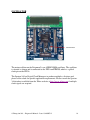
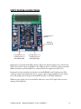
Drigmorn2 User Manual
Issue – 1.0
© Enterpoint Ltd. – Drigmorn2 Manual – Issue 1.0 06/07/12
1
Kit Contents
You should receive the following items with your Drigmorn2 development kit:
1 - Drigmorn2 Board
2 - Programming Cable
3- USB lead.
Foreword
PLEASE READ THIS ENTIRE MANUAL BEFORE PLUGGING IN
OR POWERING UP YOUR DRIGMORN2 BOARD.
PLEASE TAKE SPECIAL NOTE OF THE WARNINGS WITHIN
THIS MANUAL.
Trademarks
Spartan-3A, ISE, Webpack, EDK, COREGEN, Xilinx are the registered trademarks of Xilinx Inc,
San Jose, California, US.
Drigmorn2 is a trademark of Enterpoint Ltd.
© Enterpoint Ltd. – Drigmorn2 Manual – Issue 1.0 06/07/12
2
Contents
Kit Contents
Foreword
Trademarks
Drigmorn2 Board
Introduction
Getting Started
FPGA
SPI FLASH
SDRAM MEMORY
DIL HEADERS
USB
LCD DISPLAY
LEDS
OSCILLATOR
SWITCHES
INPUT POWER CONNECTIONS
POWER REGULATORS
PROGRAMMING DRIGMORN2
MECHANICAL
Medical and Safety Critical Use
Warranty
Support
© Enterpoint Ltd. – Drigmorn2 Manual – Issue 1.0 06/07/12
2
2
2
4
5
6
8
9
10
12
14
16
17
19
20
21
22
23
25
26
26
26
3
Drigmorn 2
© Enterpoint Ltd. – Drigmorn2 Manual – Issue 1.0 06/07/12
4
Introduction
Welcome to your Drigmorn2 board. Drigmorn2 is Enterpoint’s low cost Spartan-3A
development board. It offers a flexible and low cost approach to prototyping FPGA
and System designs.
The aim of this manual is to assist in using the main features of Drigmorn2.
There are features that are beyond the scope of the manual. Should you need to use
these features then please email [email protected] for detailed instructions.
Drigmorn2 currently comes with a XC3S1400A-4FTG256C Spartan-3A. Other
variants may be offered at a later date or as an OEM product. Smaller Spartan-3A
parts in the FT256 Package can be fitted to this board. Please contact us on
[email protected] should you need further information.
Drigmorn2 is supported by a wide range of add-on modules. Some examples of these
include:
ADC 7927 MODULE
LED DOT MATRIX MODULE
BUTTONS/SWITCHES/SATA/MEMORY MODULE
RS232 AND RS485 HEADER MODULES
DP83816 ETHERNET MODULE
SD CARD MODULE
DDR2 MODULE
IDE/5V TOLERANT CPLD MODULE
USB MODULE
D/A CONVERTER MODULE
ADV70202 MODULE
GIGABIT ETHERNET PHY MODULE
LTC2248 MODULE
MICTOR MODULE
OPTO-ISOLATOR MODULE
FT4232 QUAD USB MODULE
NAND FLASH MODULE
RTC MODULE
ACCELEROMETER MODULE
OVM CAMERA MODULE
IDT5V19EE901 CLOCK MODULE
We can also offer custom DIL Header modules should you require a function not
covered by our current range of modules. Typical turn around for this service is 6-8
weeks depending upon quantity ordered and availability of components.
© Enterpoint Ltd. – Drigmorn2 Manual – Issue 1.0 06/07/12
5
Getting Started
2X16 LCD
DISPLAY
SPARTAN-3A
FPGA
13 LEDs
USB
INTERFACE
16
POSITION
ROTARY
SWITCH
2 PUSH
BUTTON
SWITCHES
256MBIT
SDRAM
MEMORY
128M
FLASH
MEMORY
DIL HEADERS
WITH FORTY 5V
TOLERANT IO
JTAG
CONNECTOR
MINI USB
CONNECTOR
Your Drigmorn2 will be supplied un-programmed. Unless you have bought an OEM
product your board will be supplied with either a Prog2 parallel port programming
cable or a Prog3 USB port programming cable.
The Spartan-3A FPGA on board is supported by the free ISE Webpack available
from Xilinx, which provides all the tools to enter and build a design. Using this tool
in conjunction with your supplied programming cable you will also be able to
program the Spartan-3A, and the supporting SPI Flash, that are on Drigmorn2.
ISE Webpack can be obtained directly from the Xilinx website at
http://www.xilinx.com/ise. Registration will be necessary to complete the download.
Once you have obtained your ISE Webpack tools:
© Enterpoint Ltd. – Drigmorn2 Manual – Issue 1.0 06/07/12
6
(1) Connect your programming cable to the board and your PC hosting the Xilinx
software.
(2) Connect the Drigmorn2 board to either a USB connector of a PC, or a USB
power supply using the supplied USB lead. Note that some Laptops and desktop
computer USB ports have a current limit of 100mA. Drigmorn2 can exceed this
in some circumstances and should you have a problem a powered USB hub or
external mains to USB adaptor are recommended solutions.
(3) If using an external power brick switch on your power source.
© Enterpoint Ltd. – Drigmorn2 Manual – Issue 1.0 06/07/12
7
FPGA
SPARTAN-3A
FPGA
Drigmorn2 supports Spartan-3A devices in the FTG256 package. Drigmorn2 is
normally available with commercial grade -2 speed devices fitted in the XC3S700A4FTG256C size. For OEM customers we can offer a range of alternatives from
XC3S400A to XC3S1400A as custom BOM variants.
Should you have an application that needs industrial, faster speed grades, or bigger
parts please contact sales for a quote at [email protected].
© Enterpoint Ltd. – Drigmorn2 Manual – Issue 1.0 06/07/12
8
SPI FLASH MEMORY
128M FLASH
MEMORY
The M25P128 SPI flash memory device configures the FPGA when it is powered
providing a suitable bitstream is programmed into the device. The M25P128 has a
capacity of 128Mbits with a single configuration bitstream for Drigmorn2 taking
2.7Mbits (XC3S700A) . Any remaining space can be used for alternative
configurations or code and data storage.
After configuration the SPI Flash can be accessed via the following pins of the
FPGA:
M25P128
FUNCTION
CCLK
MOSI
WRITE
DIN
CSO_B
FPGA PIN
R14
P10
H16
T14
T2
The HOLD pin of this memory device is permanently connected to 3.3V.
© Enterpoint Ltd. – Drigmorn2 Manual – Issue 1.0 06/07/12
9
SDRAM MEMORY
1GBIT DDR3
Drigmorn2 has a 256MBIT SDRAM ISSI IS42S32800B-7BL device as standard.
This device is organised as 2 Meg x 32 x 4 banks. The SDRAM has 12 address lines
and 32 data lines to address all the available memory, which can be accessed at a
clock rate OF 166/143 Mhz. More details can be found in
http://www.issi.com/pdf/42s32800b.pdf
The SDRAM site has the following connections to the FPGA:
© Enterpoint Ltd. – Drigmorn2 Manual – Issue 1.0 06/07/12
10
SDRAM FUNCTION
SDRAM_A0
SDRAM_A1
SDRAM_A2
SDRAM_A3
SDRAM_A4
SDRAM_A5
SDRAM_A6
SDRAM_A7
SDRAM_A8
SDRAM_A9
SDRAM_A10
SDRAM_A11
SDRAM_A12
SDRAM_BA0
SDRAM_BA1
SDRAM_CAS_N
SDRAM_CS_N
SDRAM_RAS_N
SDRAM_WE_N
SDRAM_DQM0
SDRAM_DQM1
SDRAM_DQM2
SDRAM_DQM3
SDRAM_CKE
SDRAM_CLK
SDRAM_DQ0
SDRAM_DQ1
SDRAM_DQ2
SDRAM_DQ3
FPGA PIN
A0
A3
A7
D10
B12
A12
F14
A13
B14
C7
J13
C4
D11
F1
D4
H13
E3
D3
E1
E2
C15
F3
C12
C11
A14
E7
D8
C1
D7
SDRAM FUNCTION
SDRAM_DQ4
SDRAM_DQ5
SDRAM_DQ6
SDRAM_DQ7
SDRAM_DQ8
SDRAM_DQ9
SDRAM_DQ10
SDRAM_DQ11
SDRAM_DQ12
SDRAM_DQ13
SDRAM_DQ14
SDRAM_DQ15
SDRAM_DQ16
SDRAM_DQ17
SDRAM_DQ18
SDRAM_DQ19
SDRAM_DQ20
SDRAM_DQ21
SDRAM_DQ22
SDRAM_DQ23
SDRAM_DQ24
SDRAM_DQ25
SDRAM_DQ26
SDRAM_DQ27
SDRAM_DQ28
SDRAM_DQ29
SDRAM_DQ30
SDRAM_DQ31
© Enterpoint Ltd. – Drigmorn2 Manual – Issue 1.0 06/07/12
FPGA PIN
D1
G13
G14
C2
F13
D9
E13
D14
D13
B15
C9
C13
B3
B6
A6
B4
A5
A4
C6
C5
B10
A9
A11
C10
A10
B8
A8
C8
11
DIL HEADERS
LEFT COLUMNS
OUTER PINS
S3A INNER
ROW FUNCTION PIN PINS
1
IO_L10N_2 T8
0V
2
IO_L12N_2 T9
0V
3
IO_L12P_2 R9
0V
4
IO_L11N_2 P9
0V
5
IO_L15N_2 R11
0V
6
IO_L17N_2 P12
0V
7
IO_L18N_2 R13
0V
8
IO_L15P_2 T11
0V
9
IO_L02P_1 R15
0V
10
IO_L18P_2 T13
0V
11
IO_L16P_2 P11
0V
12
IO_L14P_2 T10
0V
13
IO_L24P_1 C16
0V
14
IO_L22N_1 D15
0V
15
IO_L22P_1 D16
0V
16
IO_L18N_1 F15
0V
17
IO_L15P_1 H15
0V
18
IO_L16P_1 G16
0V
19
IO_L16N_1 F16
0V
20
IO_L18P_2 E16
0V
RIGHT COLUMNS
OUTER PINS
INNER
S3A
PINS FUNCTION PIN
3.3V IO_L08P_2 P7
3.3V IO_L06N_2 T6
3.3V IO_L03P_2 R5
3.3V IO_L03P_2 R3
3.3V IO_L22P_3 N2
3.3V IO_L23N_3 P2
3.3V IO_L05P_2 T4
3.3V IO_L10P_2 P8
3.3V IO_L09P_2 R7
3.3V IO_L09N_2 T7
3.3V IO_L08N_2 N8
3.3V IO_L06P_2 T5
3.3V IO_L16P_3 L1
3.3V IO_L15N_3 K1
3.3V IO_L15P_3 K3
3.3V IO_L14N_3 J1
3.3V IO_L14P_3 J2
3.3V IO_L11N_3 H1
3.3V IO_L12N_3 J3
3.3V IO_L08N_3 G1
The DIL Headers provide a simple mechanical and electrical interface for add-on
modules. There are twenty I/O on each side of the DIL Header giving a total of 40
I/O available. Each of these I/O pins is protected by bus switch technology to
facilitate 5V tolerance on all of these pins. Bus switch technology has a minimal
effect on I/O timing with propagation times of less than 250ps through these devices.
The DIL Headers support the use of add-on modules enhancing the capabilities of
your Drigmorn2 board. Enterpoint has a wide range of modules suitable for the DIL
Header. We can also offer custom design modules should our standard range not
cover your requirement. The DIL Headers will also support the use of crude
prototype circuits using stripboard or other prototype materials.
© Enterpoint Ltd. – Drigmorn2 Manual – Issue 1.0 06/07/12
12
The DIL Header connectors are arranged on a standard 0.1inch (2.54mm) pitch. The
horizontal pitch of the DIL Headers is 1.6 inches between the outer rows of the
headers. The inner pins of the header form continuous power strips allowing a range
of modules to be used together in one header subject to sufficient pins being
available. The right hand side header has an inner column of 3.3V pins. The LHS
header has an inner column of DGND (0V).
© Enterpoint Ltd. – Drigmorn2 Manual – Issue 1.0 06/07/12
13
USB
FT232R USB
DEVICE
USB SOCKET
The USB interface on the Drigmorn2 is achieved using an FT232R USB to serial
UART interface. The datasheet and drivers for this device are available from
http://www.ftdichip.com. When appropriate drivers are installed the Drigmorn2 USB
port should be detected as a serial port. Alternative data optimised drivers are also
available from FTDI.
The FT232R is connected to the Spartan-3A and provided that a simple UART, or
other converter, is implemented then the data sent over the USB serial port can be
used either as control and/or data information. This allows a host computer to act in a
number of ways including system control and data storage functions.
The FT232R can also supply a clock to the Spartan-3A FPGA using CBUS4 I/O.
This I/O can be programmed by tools available from FTDI to output different
frequencies or other functions. The FT232R can provide clock frequencies of
6/12/24/48MHz.
The connections between the USB device and the FPGA are shown below:
© Enterpoint Ltd. – Drigmorn2 Manual – Issue 1.0 06/07/12
14
FT232R
CBUS4
CTS#
DCD#
DSR#
RI#
RTS#
DTR#
TXD
RXD
FPGA PIN
E4
G3
H3
K4
L4
L3
M3
N3
F4
The FT232R connections CBUS0 to CBUS3 are routed via a resistor array site
(resistor array not fitted) to the JTAG connector for future use in reconfiguring the
FPGA via a USB interface, a scenario which is theoretically possible but not so far
established. These connections, were the resistor array to be fitted, would be as
shown below:
FT232R
CBUS0
CBUS1
CBUS2
CBUS3
JTAG
SIGNAL
TDO
TDI
TMS
TCK
© Enterpoint Ltd. – Drigmorn2 Manual – Issue 1.0 06/07/12
15
LCD DISPLAY
LCD DISPLAY
The standard Drigmorn2 LCD display is an LCM-S01602DTR/M display, which is
16x2 alpha-numerical display with a Hitachi HD44780 compatible chipset. More
information on this at http://www.lumex.com/specs/LCM-S01602DTR%20M.pdf.
For OEM applications this LCD can be replaced by a 2x17 IDC header allowing
remote location of the LCD or even reuse of the interface for other I/O functions. For
these applications the 8 data signals are passed through bus switches giving 5V
tolerance. The remaining signals of this interface are not protected for 5V operation
and should only be used with voltages less than 3.3V.
The IO pins used for the display are shown in the table below:
FUNCTION
FPGA PIN
D7
P15
D6
N16
D5
N14
D4
M16
D3
M15
D2
L16
D1
L14
D0
K16
EN
N13
R/W
P13
RS
P16
© Enterpoint Ltd. – Drigmorn2 Manual – Issue 1.0 06/07/12
16
LEDS
D2
LED6
LED5
LED4
LED3
LED2
LED1
LED12
LED11
LED10
LED9
LED8
LED7
Drigmorn2 has 13 LEDs. There is a single red LED in the centre of the board just
above the FPGA, and 12 LEDs arranged into 4 blocks of three, one of each block
being red, orange and green. This is to enable users to simulate a traffic light
sequence. The LEDS may turn on dimly when power is applied to the board. The
relevant IO pin for an LED needs to be asserted high to ensure the specific LED turns
on, and High impedance ‘Z’ to turn them off.
© Enterpoint Ltd. – Drigmorn2 Manual – Issue 1.0 06/07/12
17
The LEDS are connected to the FPGA as indicated below:
LED
1
2
3
4
5
6
7
8
9
10
11
12
D2
FPGA PIN
E14
J16
K13
K14
L13
K15
L2
M1
N3
N1
P1
R1
N12
© Enterpoint Ltd. – Drigmorn2 Manual – Issue 1.0 06/07/12
COLOUR
RED
ORANGE
GREEN
GREEN
ORANGE
RED
RED
ORANGE
GREEN
GREEN
ORANGE
RED
RED (SINGLE)
18
OSCILLATOR
OSCILLATOR
The main oscillator on the Drigmorn2 is an ASEM 25MHz oscillator. The oscillator
is situated as shown and is connected to the FPGA on PIN N9, which is a global
clock pin on the FPGA.
The Spartan-3A has Digital Clock Managers to produce multiples, divisions and
phases of the clock for specific application requirements. Please consult the Spartan3A datasheet available from the Xilinx website at http://www.xilinx.com if multiple
clock signals are required.
© Enterpoint Ltd. – Drigmorn2 Manual – Issue 1.0 06/07/12
19
SWITCHES
ROTARY
SWITCH
PUSH BUTTON
SWITCH SW3
PUSH BUTTON
SWITCH SW1
The Drigmorn2 has two push button switches and one 16 position hexadecimal
rotary switch. To use these switches it is necessary to set the IO pins connected to the
switches to have a pull up resistor in the FPGA. This is set in FPGA constraints file.
Any switches pressed, or made, will then give a LOW signal at the FPGA, otherwise
a HIGH is seen. The two push button switches are connected to the following IO
pins.
SW1 (LOWER)
J4
SW3 (UPPER)
G4
The 16 position hexadecimal rotary switch bits are connected to the following IO
pins.
ROT_SW1(MSB)
J14
ROT_SW2
M11
ROT_SW3 ROT_SW4(LSB)
M13
M14
© Enterpoint Ltd. – Drigmorn2 Manual – Issue 1.0 06/07/12
20
INPUT POWER CONNECTIONS
ANCILLIARY 5V
PICKUP
MINI USB
CONNECTOR
COLUMN OF 20 0V
CONNECTIONS ON
LHS DILHEADER
COLUMN OF 20 3.3V
CONNECTIONS ON
RHS DILHEADER
Drigmorn2 is powered from the USB connector. The board should be plugged via a cable into the
USB socket of a PC, Laptop or USB hub. Some USB ports may not be able to supply greater than
100mA and either a powered USB hub or a mains wall brick is suggested for these cases.
Drigmorn2 also has an ancillary 2 pin header site with DGND(0V) and 5V pickup points. This
connector normally not fitted but can used as a power output or input depending on your design
needs. The pickup point is aligned to the main DIL Headers on a 01inch/2.54mm grid.
Whatever power supply is used care should be taken not to exceed 5.5V input as this can cause
damage to the Drigmorn2.
© Enterpoint Ltd. – Drigmorn2 Manual – Issue 1.0 06/07/12
21
POWER REGULATORS
1.2V
REGULATOR
3.3V
REGULATOR
Drigmorn2 has two regulators supplying 3.3V and1.2V power rails.
WARNING – REGULATORS CAN BECOME HOT IN NORMAL
OPERATION ALONG WITH THE BOARDS THERMAL RELIEF. PLEASE
DO NOT TOUCH OR PLACE HIGHLY FLAMABLE MATERIALS NEAR
THESE DEVICES WHILST THE DRIGMORN2 BOARD IS IN OPERATION.
An Empirion EP5388QI regulator supplies 3.3V with a maximum current available of
800mA. This powers the FPGA general I/O, SDRAM, DIL Headers and other
devices such the Ethernet controller and Real Time Clock.
A Micrel MIC33050 regulator supplies 1.2V with a maximum current of 600mA for
the core voltage of the FPGA .
If you are using these power rails to provide power to add-on modules or your own
circuitry via the DIL headers you should always ensure that you do not exceed the
maximum current output of these regulators.
© Enterpoint Ltd. – Drigmorn2 Manual – Issue 1.0 06/07/12
22
Programming Drigmorn2
JTAG Header
The programming of the FPGA and SPI Flash parts on Drigmorn2 is achieved using
the JTAG interface. Principally it is anticipated that a JTAG connection will be used
in conjunction with Xilinx ISE software. The free Webpack version of the Xilinx
tools can be used to program the Drigmorn2.
There is a single JTAG chain on Drigmorn2. The JTAG chain allows the
programming of the Spartan-3A and the SPI Flash device.
The JTAG connector has a layout as follows (top view):
GND
NC
GND
NC
GND
TDI
GND
TDO
GND
TCK
GND
TMS
GND
3V3
Using iMPACT Boundary Scan the JTAG chain appears like this:
© Enterpoint Ltd. – Drigmorn2 Manual – Issue 1.0 06/07/12
23
1. Programming the FPGA directly.
Direct JTAG programming of the Spartan-3A FPGA is volatile and the FPGA will
lose its configuration every time the board power is cycled. For sustained use of an
FPGA design programming the design into the Flash memory is recommended (see 2
and 3 below).
Direct JTAG programming using .bit files is useful for fast, temporary programming
during development of FPGA programs. Right click the icon representing the
Spartan-3A FPGA and choose ‘Assign New Configuration File’. Navigate to your .bit
file and choose ‘OPEN’. The next dialogue box will offer to add a flash memory and
you should decline. Right click the icon representing the Spartan-3A FPGA and
choose ‘Program’. On the next dialogue box ensure that the ‘Verify’ box is not
checked. (If it is you should uncheck it, failure to do this will result in error messages
being displayed). Click OK. The Spartan-3A will program. This process is very quick
(typically one second)
2. Programming the SPI flash memory using Boundary Scan.
Once the SPI Flash memory has been programmed, the Spartan-3A device will
automatically load from the Flash memory at power up. Generation of suitable Flash
memory files (.mcs) can be achieved using ISE iMPACT’s Prom File Formatter.
Right click on the icon representing the Spartan-3A and choose ‘Add SPI/BPI Flash’
Navigate to your programming file (.mcs) and click OPEN. Use the next dialogue
box to select SPI flash and M25P128. Data width should be set to 1. The flash
memory should appear as shown below.
Right click on the icon representing the flash memory and choose program to load
your program into the device. It is recommended that options to ‘Verify’ and ‘Erase
before programming’ are chosen. Otherwise all defaults can be accepted. The
programming operation will take some time (at least 3 or 4 minutes)
© Enterpoint Ltd. – Drigmorn2 Manual – Issue 1.0 06/07/12
24
MECHANICAL ARRANGEMENT
The Dimensions on the drawing below are millimetres (mm). All sizes quoted are
subject to manufacturing tolerances and should only be used as a general guide.
The heights of the components, measured from the lower surface of the board are as
follows:
Upper surface of LCD display: 12.5mm
The PCB is 1.6mm thick
Mechanical Arrangement of DIL headers
The socket pins on the DIL headers are arranged on a 2.45mm (0.1inch) pitch
© Enterpoint Ltd. – Drigmorn2 Manual – Issue 1.0 06/07/12
25
Medical and Safety Critical Use
Drigmorn2 boards are not authorised for the use in, or use in the design of, medical or
other safety critical systems without the express written person of the Board of
Enterpoint. If such use is allowed the said use will be entirely the responsibility of the
user. Enterpoint Ltd will accept no liability for any failure or defect of the Drigmorn2
board, or its design, when it is used in any medical or safety critical application.
Warranty
Drigmorn2 comes with a 90 day return to base warranty. Do not attempt to solder
connections to the Drigmorn2. Enterpoint reserves the right not honour a warranty if
the failure is due to soldering or other maltreatment of the Drigmorn2 board.
Outside warranty Enterpoint offers a fixed price repair or replacement service. We
reserve the right not to offer this service where a Drigmorn2 has been maltreated or
otherwise deliberately damaged. Please contact support if you need to use this
service.
Other specialised warranty programs can be offered to users of multiple Enterpoint
products. Please contact sales on [email protected] if you are interested in
these types of warranty,
Support
Telephone and email support is offered during normal United Kingdom working
hours (GMT or GMT + 1) 9.00am to 5.00pm.
Telephone - +44 (0) 121 288 3945
Email
- [email protected]
© Enterpoint Ltd. – Drigmorn2 Manual – Issue 1.0 06/07/12
26