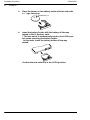
1
Safety Precautions
Observe the following notices to ensure personal safety or to prevent accidents.
To ensure that you use this product correctly, read this User’s Manual thoroughly before use.
Make sure that you fully understand the product and information on safety.
This manual uses two safety flags to indicate different levels of danger.
WARNING
If critical situations that could lead to user’s death or serious injury is assumed by
mishandling of the product.
-Always take precautions to ensure the overall safety of your system, so that the whole
system remains safe in the event of failure of this product or other external factor.
-Do not use this product in areas with inflammable gas. It could lead to an explosion.
-Exposing this product to excessive heat or open flames could cause damage to the lithium
battery or other electronic parts.
-Battery may explode if mistreated. Do not recharge, disassemble or dispose of fire.
CAUTION
If critical situations that could lead to user’s injury or only property damage is
assumed by mishandling of the product.
-To prevent excessive exothermic heat or smoke generation, use this product at the values
less than the maximum of the characteristics and performance that are assured in these
specifications.
-Do not dismantle or remodel the product. It could cause excessive exothermic heat or smoke
generation.
-Do not touch the terminal while turning on electricity. It could lead to an electric shock.
-Use the external devices to function the emergency stop and interlock circuit.
-Connect the wires or connectors securely.
The loose connection could cause excessive exothermic heat or smoke generation.
-Ground the protective earth (PE) terminal (Class D grounding). Failure to do so could lead to
an electric shock.
-Do not allow foreign matters such as liquid, flammable materials, metals to go into the inside
of the product. It could cause excessive exothermic heat or smoke generation.
-Do not undertake construction (such as connection and disconnection) while the power
supply is on. It could lead to an electric shock.
Copyright / Trademarks
-This manual and its contents are copyrighted.
-You may not copy this manual, in whole or part, without written consent of Panasonic
Industrial Devices SUNX Co., Ltd.
-Windows is a registered trademark of Microsoft Corporation in the United States and other
countries.
-All other company names and product names are trademarks or registered trademarks of
their respective owners.
PLC_BATPE
FP2/FP2SH
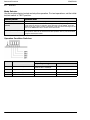
Table of Figures
Table of Contents
Before You Start . . . . . . . . . . . . . . . . . . . . . . . . . . . . . . . . . . . . . . . . . . . . . . . . . . . . viii
Special Precautions . . . . . . . . . . . . . . . . . . . . . . . . . . . . . . . . . . . . . . . . . . . . . . . . . x
Compatibility with CPU Unit, and Precautions . . . . . . . . . . . . . . . . . xiii
Compatibility of FP2SH and FP2, and Precautions . . . . . . . . . . . xiv
IC memory cards for the FP2SH . . . . . . . . . . . . . . . . . . . . . . . . . . . . . . . . . . xv
Compatibility of FP2/FP2SH and FP10SH, and Precautions . xvi
Programming Tool Restrictions . . . . . . . . . . . . . . . . . . . . . . . . . . . . . . . . . xvii
Chapter 1
Overview
1.1
System Configuration . . . . . . . . . . . . . . . . . . . . . . . . . . . . . . . . . . . . . . . . . . . . . . 1 − 3
1.1.1
Basic Configuration by Number of Slots . . . . . . . . . . . . . . . . . . . . . . 1 − 3
1.1.2
Expansion of Backplane . . . . . . . . . . . . . . . . . . . . . . . . . . . . . . . . . . . . 1 − 5
1.2
Unit Types and Combinations . . . . . . . . . . . . . . . . . . . . . . . . . . . . . . . . . . . . . . . 1 − 8
1.2.1
Line-Up of Backplanes and Units . . . . . . . . . . . . . . . . . . . . . . . . . . . . 1 − 8
1.2.2
Combinations That Can be Used and Restrictions . . . . . . . . . . . 1 − 10
1.2.2.1
Restrictions on Unit Types . . . . . . . . . . . . . . . . . . . . . . 1 − 10
1.2.2.2
Limitations on Current Consumption . . . . . . . . . . . . . 1 − 12
1.3
Expansion Function . . . . . . . . . . . . . . . . . . . . . . . . . . . . . . . . . . . . . . . . . . . . . 1 − 15
1.3.1
Computer Link . . . . . . . . . . . . . . . . . . . . . . . . . . . . . . . . . . . . . . . . . . 1 − 15
1.3.2
Connection of MODEM . . . . . . . . . . . . . . . . . . . . . . . . . . . . . . . . . . . 1 − 17
1.4
Programming Tools . . . . . . . . . . . . . . . . . . . . . . . . . . . . . . . . . . . . . . . . . . . . . .
1.4.1
Tools Needed for Programming . . . . . . . . . . . . . . . . . . . . . . . . . . . .
1.4.2
Software Environment and Suitable Cable . . . . . . . . . . . . . . . . . .
1.4.3
Tools Needed for ROM Creating . . . . . . . . . . . . . . . . . . . . . . . . . . .
Chapter 2
1 − 19
1 − 19
1 − 20
1 − 21
Parts and Functions
2.1
Backplane and Expansion Cable . . . . . . . . . . . . . . . . . . . . . . . . . . . . . . . . . . . . 2 − 3
2.1.1
Backplane . . . . . . . . . . . . . . . . . . . . . . . . . . . . . . . . . . . . . . . . . . . . . . . . 2 − 3
2.1.2
Basic Backplane H Type (FP2−BP**MH) . . . . . . . . . . . . . . . . . . . . . . 2 − 5
2.1.3
Expansion Backplane H Type (FP2−BP**EH) . . . . . . . . . . . . . . . . . . 2 − 6
2.1.4
Expansion Cable . . . . . . . . . . . . . . . . . . . . . . . . . . . . . . . . . . . . . . . . . . 2 − 7
2.2
FP2 CPU . . . . . . . . . . . . . . . . . . . . . . . . . . . . . . . . . . . . . . . . . . . . . . . . . . . . . . . . 2 − 8
2.2.1
Standard Type CPU (FP2−C1) . . . . . . . . . . . . . . . . . . . . . . . . . . . . . . 2 − 8
2.2.2
CPU with 64 Points Input (FP2−C1D) . . . . . . . . . . . . . . . . . . . . . . 2 − 12
i
Table of Contents
FP2/FP2SH
2.3
2.4
Expansion Memory Unit and ROM (for FP2 CPU) . . . . . . . . . . . . . . . . . . .
FP2SH CPU . . . . . . . . . . . . . . . . . . . . . . . . . . . . . . . . . . . . . . . . . . . . . . . . . . .
2.4.1
32k/60k Step Standard Type CPU (FP2-C2L/FP2-C2) . . . . . . . .
2.4.2
CPU with IC Memory Card Interface (FP2-C2P/FP2−C3P) . . . .
2.5 Expansion Memory Unit and ROM (for FP2−C2L/FP2-C2) . . . . . . . . . . . .
2.6 IC Memory Card (for FP2-C2P/FP2-C3P) . . . . . . . . . . . . . . . . . . . . . . . . . . .
2.7 Power Supply Units . . . . . . . . . . . . . . . . . . . . . . . . . . . . . . . . . . . . . . . . . . . . .
2.7.1
Power Supply Specifications . . . . . . . . . . . . . . . . . . . . . . . . . . . . . .
2.8 Input and Output Units . . . . . . . . . . . . . . . . . . . . . . . . . . . . . . . . . . . . . . . . . . .
2.8.1
Common Specifications of Input and Output Units . . . . . . . . . . . .
2.9 Input Units Specifications . . . . . . . . . . . . . . . . . . . . . . . . . . . . . . . . . . . . . . . .
2.9.1
16-point Type DC Input Unit . . . . . . . . . . . . . . . . . . . . . . . . . . . . . . .
2.9.2
32-point Type DC Input Unit . . . . . . . . . . . . . . . . . . . . . . . . . . . . . . .
2.9.3
64-point Type DC Input Unit . . . . . . . . . . . . . . . . . . . . . . . . . . . . . . .
2.10 Output Units Specifications . . . . . . . . . . . . . . . . . . . . . . . . . . . . . . . . . . . . . . .
2.10.1 16-point Type Relay Output Unit . . . . . . . . . . . . . . . . . . . . . . . . . . .
2.10.2 6-point Type Relay Output Unit . . . . . . . . . . . . . . . . . . . . . . . . . . . .
2.10.3 16-point Type Transistor (NPN) Output Unit . . . . . . . . . . . . . . . . .
2.10.4 16-point Type Transistor (PNP) Output Unit . . . . . . . . . . . . . . . . .
2.10.5 32-point Type Transistor (NPN) Output Unit . . . . . . . . . . . . . . . . .
2.10.6 32-point Type Transistor (PNP) Output Unit . . . . . . . . . . . . . . . . .
2.10.7 64-point Type Transistor (NPN) Output Unit . . . . . . . . . . . . . . . . .
2.10.8 64-point Type Transistor (PNP) Output Unit . . . . . . . . . . . . . . . . .
2.11 I/O Mixed Units Specifications . . . . . . . . . . . . . . . . . . . . . . . . . . . . . . . . . . . .
2.11.1 32−point Type DC Input/32−point Type Transistor (NPN)
Output Unit . . . . . . . . . . . . . . . . . . . . . . . . . . . . . . . . . . . . . . . . . . . . .
2.11.2 32−point Type DC Input/32−point Type Transistor (PNP)
Output Unit . . . . . . . . . . . . . . . . . . . . . . . . . . . . . . . . . . . . . . . . . . . . .
2.11.3 32−point Type DC Input with On Pulse Catch Input Function/
32−point Type Transistor Output (NPN) Unit . . . . . . . . . . . . . . . . .
2.11.4 32−point Type DC Input with On Pulse Catch Input Function/
32−point Type Transistor Output (PNP) Unit . . . . . . . . . . . . . . . . .
2.11.5 On Pulse Catch Input Function . . . . . . . . . . . . . . . . . . . . . . . . . . . .
Chapter 3
3.1
3.2
ii
2 − 15
2 − 18
2 − 19
2 − 20
2 − 22
2 − 23
2 − 28
2 − 28
2 − 30
2 − 30
2 − 33
2 − 33
2 − 35
2 − 37
2 − 39
2 − 39
2 − 41
2 − 43
2 − 45
2 − 47
2 − 49
2 − 51
2 − 53
2 − 55
2 − 55
2 − 58
2 − 61
2 − 64
2 − 67
I/O Allocation
Fundamentals of I/O Allocation . . . . . . . . . . . . . . . . . . . . . . . . . . . . . . . . . . . . . . 3 − 3
3.1.1
I/O Allocation and Registering . . . . . . . . . . . . . . . . . . . . . . . . . . . . . . . 3 − 3
3.1.1.1
Types of I/O Allocation Methods . . . . . . . . . . . . . . . . . . . 3 − 3
3.1.1.2
Precautions Regarding Registering of I/O Allocation . 3 − 3
3.1.1.3
How to Count the I/O Numbers and Express the
Occupied Points . . . . . . . . . . . . . . . . . . . . . . . . . . . . . . . . 3 − 4
3.1.2
Table of Occupied I/O Points by Unit . . . . . . . . . . . . . . . . . . . . . . . . . 3 − 5
Arbitrary Allocation . . . . . . . . . . . . . . . . . . . . . . . . . . . . . . . . . . . . . . . . . . . . . . . . 3 − 7
3.2.1
Using Arbitrary Allocation . . . . . . . . . . . . . . . . . . . . . . . . . . . . . . . . . . . 3 − 7
FP2/FP2SH
Table of Figures
3.2.2
3.2.3
3.3
3.4
3.5
3.6
Allocation Example of CPU Backplane . . . . . . . . . . . . . . . . . . . . . . . 3 − 7
Allocation Example of Expansion Backplane . . . . . . . . . . . . . . . . 3 − 10
3.2.3.1
When Using FP2 Backplane . . . . . . . . . . . . . . . . . . . . 3 − 10
3.2.3.2
When Using FP2 Backplane H Type . . . . . . . . . . . . . . 3 − 11
I/O Mount Allocation . . . . . . . . . . . . . . . . . . . . . . . . . . . . . . . . . . . . . . . . . . . . . 3 − 13
3.3.1
Using I/O Mount Allocation . . . . . . . . . . . . . . . . . . . . . . . . . . . . . . . . 3 − 13
3.3.1.1
Example of I/O Mount Allocation . . . . . . . . . . . . . . . . 3 − 13
3.3.1.2
Procedure for I/O Mount Allocation . . . . . . . . . . . . . . 3 − 14
Automatic Allocation . . . . . . . . . . . . . . . . . . . . . . . . . . . . . . . . . . . . . . . . . . . . . 3 − 15
3.4.1
Using Automatic Allocation . . . . . . . . . . . . . . . . . . . . . . . . . . . . . . . 3 − 15
3.4.1.1
Example of Automatic Allocation . . . . . . . . . . . . . . . . 3 − 15
3.4.1.2
Procedure for Automatic Allocation . . . . . . . . . . . . . . 3 − 16
Procedure for Clearing Registered Content . . . . . . . . . . . . . . . . . . . . . . . . . 3 − 17
3.5.1
Meaning of Clearing Registered Content . . . . . . . . . . . . . . . . . . . . 3 − 17
3.5.2
Clearing Content Using Programming Tool Software . . . . . . . . . 3 − 17
I/O Numbers of Free Slots . . . . . . . . . . . . . . . . . . . . . . . . . . . . . . . . . . . . . . . . 3 − 18
3.6.1
I/O Numbers of Free Slots . . . . . . . . . . . . . . . . . . . . . . . . . . . . . . . . 3 − 18
3.6.2
Differences Due to Allocation Methods . . . . . . . . . . . . . . . . . . . . . 3 − 18
3.6.2.1
When Arbitrary Allocation is Used . . . . . . . . . . . . . . . 3 − 18
3.6.2.2
When I/O Mount Allocation is Used . . . . . . . . . . . . . . 3 − 20
3.6.2.3
When Automatic Allocation is Used . . . . . . . . . . . . . . 3 − 21
Chapter 4
4.1
4.2
4.3
4.4
4.5
Installation and Wiring
Installation . . . . . . . . . . . . . . . . . . . . . . . . . . . . . . . . . . . . . . . . . . . . . . . . . . . . . . . 4 − 3
4.1.1
Installation Space and Environment . . . . . . . . . . . . . . . . . . . . . . . . . . 4 − 3
4.1.2
Mounting Method . . . . . . . . . . . . . . . . . . . . . . . . . . . . . . . . . . . . . . . . . . 4 − 6
4.1.2.1
Backplane . . . . . . . . . . . . . . . . . . . . . . . . . . . . . . . . . . . . . . 4 − 6
4.1.2.2
Units . . . . . . . . . . . . . . . . . . . . . . . . . . . . . . . . . . . . . . . . . . 4 − 8
4.1.3
Connecting Expansion Cable . . . . . . . . . . . . . . . . . . . . . . . . . . . . . . 4 − 11
4.1.4
Preparing the Backup Battery . . . . . . . . . . . . . . . . . . . . . . . . . . . . . 4 − 13
Power Supply Wiring . . . . . . . . . . . . . . . . . . . . . . . . . . . . . . . . . . . . . . . . . . . . 4 − 15
4.2.1
Wiring of Power Supply . . . . . . . . . . . . . . . . . . . . . . . . . . . . . . . . . . 4 − 15
4.2.2
Grounding . . . . . . . . . . . . . . . . . . . . . . . . . . . . . . . . . . . . . . . . . . . . . . 4 − 17
Wiring Input and Output . . . . . . . . . . . . . . . . . . . . . . . . . . . . . . . . . . . . . . . . . . 4 − 18
4.3.1
Input Wiring . . . . . . . . . . . . . . . . . . . . . . . . . . . . . . . . . . . . . . . . . . . . . 4 − 18
4.3.2
Output Wiring . . . . . . . . . . . . . . . . . . . . . . . . . . . . . . . . . . . . . . . . . . . 4 − 21
4.3.3
Cautions Regarding Units . . . . . . . . . . . . . . . . . . . . . . . . . . . . . . . . 4 − 22
Wiring the Connector Type I/O Units . . . . . . . . . . . . . . . . . . . . . . . . . . . . . . . 4 − 23
4.4.1
Wiring the Connector Type Units . . . . . . . . . . . . . . . . . . . . . . . . . . 4 − 23
4.4.2
Connecting with Connector for Wire-pressed Terminal Cable . . 4 − 25
4.4.3
Connecting the Terminals . . . . . . . . . . . . . . . . . . . . . . . . . . . . . . . . . 4 − 27
4.4.4
Connecting with Flat Cable Connector . . . . . . . . . . . . . . . . . . . . . . 4 − 32
Wiring the Terminal Block Type I/O Units . . . . . . . . . . . . . . . . . . . . . . . . . . . 4 − 34
iii
Table of Contents
4.5.1
4.6
FP2/FP2SH
Wiring the Terminal Block Type Units . . . . . . . . . . . . . . . . . . . . . . . 4 − 34
Safety Measures . . . . . . . . . . . . . . . . . . . . . . . . . . . . . . . . . . . . . . . . . . . . . . . .
4.6.1
Safety Instructions . . . . . . . . . . . . . . . . . . . . . . . . . . . . . . . . . . . . . . .
4.6.2
Momentary Power Failures . . . . . . . . . . . . . . . . . . . . . . . . . . . . . . .
4.6.3
Alarm Output . . . . . . . . . . . . . . . . . . . . . . . . . . . . . . . . . . . . . . . . . . .
Chapter 5
4 − 36
4 − 36
4 − 37
4 − 37
Procedure Until Operation
5.1
Before Turning ON the Power . . . . . . . . . . . . . . . . . . . . . . . . . . . . . . . . . . . . . . . 5 − 3
5.1.1
Check Items . . . . . . . . . . . . . . . . . . . . . . . . . . . . . . . . . . . . . . . . . . . . . . 5 − 3
5.1.2
Procedure Up To Operation . . . . . . . . . . . . . . . . . . . . . . . . . . . . . . . . . 5 − 4
5.2
Programming with Programming Tool Software . . . . . . . . . . . . . . . . . . . . . . . . 5 − 5
5.2.1
Preparations . . . . . . . . . . . . . . . . . . . . . . . . . . . . . . . . . . . . . . . . . . . . . . 5 − 5
5.2.2
Configuration of Programming Tool Software . . . . . . . . . . . . . . . . . . 5 − 6
5.2.2.1
Parameters and Setting Methods . . . . . . . . . . . . . . . . . . 5 − 6
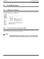
Chapter 6
FP2/FP2SH Operation
6.1
FP2 Operation . . . . . . . . . . . . . . . . . . . . . . . . . . . . . . . . . . . . . . . . . . . . . . . . . . . . 6 − 3
6.1.1
FP2 RAM and ROM Operations . . . . . . . . . . . . . . . . . . . . . . . . . . . . . 6 − 3
6.1.1.1
Comparison of RAM and ROM Operations . . . . . . . . . . 6 − 3
6.1.1.2
Retaining the Data During Power Outages . . . . . . . . . . 6 − 4
6.1.1.3
Setting the Battery Error Warnings . . . . . . . . . . . . . . . . . 6 − 4
6.2
FP2 RAM Operation . . . . . . . . . . . . . . . . . . . . . . . . . . . . . . . . . . . . . . . . . . . . . . . 6 − 5
6.2.1
RAM Operation Method . . . . . . . . . . . . . . . . . . . . . . . . . . . . . . . . . . . . 6 − 5
6.2.2
Precautions When Operating the RAM . . . . . . . . . . . . . . . . . . . . . . . 6 − 5
6.3
FP2 ROM Operation . . . . . . . . . . . . . . . . . . . . . . . . . . . . . . . . . . . . . . . . . . . . . . . 6 − 6
6.3.1
ROM Operation Method . . . . . . . . . . . . . . . . . . . . . . . . . . . . . . . . . . . . 6 − 6
6.3.2
Verifying the ROM Contents in RAM Operation . . . . . . . . . . . . . . . . 6 − 7
6.4
Writing to ROM . . . . . . . . . . . . . . . . . . . . . . . . . . . . . . . . . . . . . . . . . . . . . . . . . . . 6 − 8
6.4.1
Writing to EPROM Using Programming Tool Software . . . . . . . . . . 6 − 8
6.4.2
Writing to EPROM via FROM . . . . . . . . . . . . . . . . . . . . . . . . . . . . . 6 − 10
6.5
FP2SH Operation . . . . . . . . . . . . . . . . . . . . . . . . . . . . . . . . . . . . . . . . . . . . . . .
6.5.1
Comparison of RAM, ROM, and IC Memory Card Operation . . .
6.5.2
Retaining Data If the Power Fails . . . . . . . . . . . . . . . . . . . . . . . . . .
6.5.3
Comment Function . . . . . . . . . . . . . . . . . . . . . . . . . . . . . . . . . . . . . .
6.6
FP2SH RAM Operation . . . . . . . . . . . . . . . . . . . . . . . . . . . . . . . . . . . . . . . . . . 6 − 17
6.6.1
RAM Operation Method . . . . . . . . . . . . . . . . . . . . . . . . . . . . . . . . . . 6 − 17
6.6.2
Precautions When Operating the RAM . . . . . . . . . . . . . . . . . . . . . 6 − 18
6.7
FP2SH ROM Operation . . . . . . . . . . . . . . . . . . . . . . . . . . . . . . . . . . . . . . . . . . 6 − 19
iv
6 − 13
6 − 13
6 − 14
6 − 16
FP2/FP2SH
6.7.1
6.7.2
6.7.3
6.7.4
6.7.5
6.7.6
ROM Operation Function . . . . . . . . . . . . . . . . . . . . . . . . . . . . . . . . .
ROM Operation Method . . . . . . . . . . . . . . . . . . . . . . . . . . . . . . . . . .
Precautions When Operating the ROM . . . . . . . . . . . . . . . . . . . . .
Checking the ROM Contents While Using RAM Operation . . . .
Sending Data from the RAM to the FROM . . . . . . . . . . . . . . . . . .
Writing Data to the ROM (AFP5209) (only the FP2−C2
can be installed) . . . . . . . . . . . . . . . . . . . . . . . . . . . . . . . . . . . . . . . . .
Writing Data to the ROM: Using the FPWIN GR . . . . . . . . . . . . .
6 − 19
6 − 20
6 − 21
6 − 22
6 − 23
FP2SH IC Memory Card Operation (for FP2−C2P/FP2−C3P) . . . . . . . . .
6.8.1
Operating Using the IC Memory Card . . . . . . . . . . . . . . . . . . . . . .
6.8.2
Creating Files for Automatically Run Programs . . . . . . . . . . . . . .
6.8.3
How the IC Memory Card is Operated . . . . . . . . . . . . . . . . . . . . . .
6.8.4
Transferring Data From the RAM to the IC Memory Card . . . . . .
6 − 29
6 − 29
6 − 31
6 − 32
6 − 33
6.7.7
6.8
Table of Figures
Chapter 7
6 − 25
6 − 27
IC Memory Card
7.1
Using the IC Memory Card . . . . . . . . . . . . . . . . . . . . . . . . . . . . . . . . . . . . . . . . . 7 − 3
7.1.1
Types of IC Memory Cards . . . . . . . . . . . . . . . . . . . . . . . . . . . . . . . . . 7 − 3
7.1.2
Using the IC Memory Card . . . . . . . . . . . . . . . . . . . . . . . . . . . . . . . . . . 7 − 4
7.2
Formatting and Erasing . . . . . . . . . . . . . . . . . . . . . . . . . . . . . . . . . . . . . . . . . . . . 7 − 6
7.2.1
Program Memory Field and Expanded Memory Field . . . . . . . . . . . 7 − 6
7.2.2
Procedure for Formatting the IC Memory Card . . . . . . . . . . . . . . . . . 7 − 8
7.2.3
Procedure for Erasing the IC Memory Card . . . . . . . . . . . . . . . . . . 7 − 11
7.2.4
Data Storage Capacity of IC Memory Card . . . . . . . . . . . . . . . . . . 7 − 12
7.3
For Use as Program Memory . . . . . . . . . . . . . . . . . . . . . . . . . . . . . . . . . . . . . 7 − 13
7.3.1
Writing the Program . . . . . . . . . . . . . . . . . . . . . . . . . . . . . . . . . . . . . 7 − 13
7.3.2
Reading the Program . . . . . . . . . . . . . . . . . . . . . . . . . . . . . . . . . . . . 7 − 18
7.4
For Use as Expansion Memory . . . . . . . . . . . . . . . . . . . . . . . . . . . . . . . . . . . . 7 − 22
7.5
Menus Related to Tool Software . . . . . . . . . . . . . . . . . . . . . . . . . . . . . . . . . . . 7 − 25
Chapter 8
Self-Diagnostic Function and Troubleshooting
8.1
Self-Diagnostic Function . . . . . . . . . . . . . . . . . . . . . . . . . . . . . . . . . . . . . . . . . . . 8 − 3
8.1.1
LED Display for Status Condition . . . . . . . . . . . . . . . . . . . . . . . . . . . . 8 − 3
8.1.2
Operation When an Error Occurs . . . . . . . . . . . . . . . . . . . . . . . . . . . . 8 − 4
8.2
Troubleshooting . . . . . . . . . . . . . . . . . . . . . . . . . . . . . . . . . . . . . . . . . . . . . . . . . . . 8 − 5
8.2.1
If the ERROR LED Lights . . . . . . . . . . . . . . . . . . . . . . . . . . . . . . . . . . . 8 − 5
8.2.2
If the ALARM LED Lights . . . . . . . . . . . . . . . . . . . . . . . . . . . . . . . . . . . 8 − 7
8.2.3
If the LED (POWER) of the Power Supply Unit Does Not Light . . . 8 − 7
v
Table of Contents
8.2.4
8.2.5
8.2.6
Chapter 9
9.1
9.2
FP2/FP2SH
If Outputting Does Not Occur as Desired . . . . . . . . . . . . . . . . . . . . . 8 − 8
If a Communication Error Message Appears . . . . . . . . . . . . . . . . . . 8 − 9
If a Protect Error Message Appears . . . . . . . . . . . . . . . . . . . . . . . . 8 − 10
Maintenance
Replacement of Spare Parts . . . . . . . . . . . . . . . . . . . . . . . . . . . . . . . . . . . . . . . . 9 − 3
9.1.1
Backup Battery . . . . . . . . . . . . . . . . . . . . . . . . . . . . . . . . . . . . . . . . . . . . 9 − 3
9.1.2
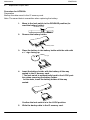
Removable Terminal Block for Input and Output Units . . . . . . . . . . 9 − 7
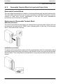
Preventive Maintenance . . . . . . . . . . . . . . . . . . . . . . . . . . . . . . . . . . . . . . . . . . . 9 − 8
Chapter 10 Specifications
10.1 Specifications . . . . . . . . . . . . . . . . . . . . . . . . . . . . . . . . . . . . . . . . . . . . . . . . . . . 10 − 3
10.2 Relays, Memory Areas and Constants . . . . . . . . . . . . . . . . . . . . . . . . . . . . 10 − 10
10.3 Cable/Adapter Specifications . . . . . . . . . . . . . . . . . . . . . . . . . . . . . . . . . . . . 10 − 13
10.3.1 AFC8503/AFC8503S . . . . . . . . . . . . . . . . . . . . . . . . . . . . . . . . . . . 10 − 13
10.3.2 AFC85305/AFC8531/AFC8532
(For extending for the tool port) . . . . . . . . . . . . . . . . . . . . . . . . . . . 10 − 13
Chapter 11 Appendix
11.1 System Registers/Special Internal Relays/Special Data Registers . . . . . . 11 - 2
11.1.1 Table of System Registers for FP2/FP2SH/FP10SH . . . . . . . . . . . 11 − 4
11.1.2 Table of Special Internal Relays for FP2/FP2SH/FP10SH . . . . 11 − 18
11.1.3 Special Data Registers for FP2/FP2SH/FP10SH/FP3 . . . . . . . . 11 − 29
11.2 Table of Basic Instructions . . . . . . . . . . . . . . . . . . . . . . . . . . . . . . . . . . . . . . . 11 − 54
11.3 Table of High−level Instructions . . . . . . . . . . . . . . . . . . . . . . . . . . . . . . . . . . 11 − 62
11.4 Table of Error codes . . . . . . . . . . . . . . . . . . . . . . . . . . . . . . . . . . . . . . . . . . . . 11 − 82
11.4.1 Table of Syntax Check Error . . . . . . . . . . . . . . . . . . . . . . . . . . . . . 11 − 84
11.4.2 Table of Self−Diagnostic Error . . . . . . . . . . . . . . . . . . . . . . . . . . . . 11 − 86
11.4.3 Table of MEWTOCOL−COM Communication Error . . . . . . . . . . 11 − 93
11.5 MEWTOCOL−COM Communication Commands . . . . . . . . . . . . . . . . . . . 11 − 95
11.6 Hexadecimal/Binary/BCD . . . . . . . . . . . . . . . . . . . . . . . . . . . . . . . . . . . . . . . 11 − 96
11.7 ASCII Codes . . . . . . . . . . . . . . . . . . . . . . . . . . . . . . . . . . . . . . . . . . . . . . . . . . 11 − 97
Index . . . . . . . . . . . . . . . . . . . . . . . . . . . . . . . . . . . . . . . . . . . . . . . . . . . . . . . . . . . . . . . . . . . . . .
Record of changes
vi
I−1
................................................... R−1
FP2/FP2SH
Table of Figures
Before You Start
Operating environment
(Use the unit within the range of the general specifications when installing)
• Ambient temperatures:0 to +55 °C
• Ambient humidity: 30% to 85% RH (at 25 °C, non−condensing)
• For use in pollution Degree 2 environment.
• Do not use it in the following environments.
− Direct sunlight
− Sudden temperature changes causing condensation.
− Inflammable or corrosive gas.
− Excessive airborne dust, metal particles or saline matter.
− Benzine, paint thinner, alcohol or other organic solvents or
strong alkaline solutions such as ammonia or caustic soda.
− Direct vibration, shock or direct drop of water.
− Influence from power transmission lines, high voltage
equipment, power cables, power equipment, radio transmitters,or
any other equipment that would generate high switching surges.
(100mm or more)
About static electricity
• Do not touch connector pins directly to prevent static electricity
from causing damage.
• Always rid yourself of any static electricity before handling this
product.
Wiring the Power Supply to the Control Unit
• Use a power supply wire that is thicker than 2 mm2 (AWG14), and
twist it.
• The unit has sufficient noise immunity against the noise generated
on the power line.
However, it is recommended to take measures for reducing noise
such as using a isolating transformer before supplying the power.
• Allocate an independent wiring for each power supplying line,
input/output device and operating device.
If using a power supply without a protective circuit, power should
be supplied through a protective element such as a fuse.
• Use the same power supply system for the CPU backplane and
expansion backplane so that they are turned on and off
simultaneously.
vii
Table of Contents
FP2/FP2SH
Power supply sequence
• In order to protect the power supply sequence, make sure to turn
off the PLC before the input/output power supply. If the input/output
power supply is turned off before the PLC, or if the PLC is not shut
off momentarily, the controller detects change of input level, and
might conduct an unexpected operation.
Before Turning On the Power (
Chapter 4 and Chapter 5)
When turning on the power for the first time, be sure to take the precautions given below.
• When performing installation, check to make sure that there are no
scraps of wiring, particularly conductive fragments, adhering to the
unit.
• Verify that the power supply wiring, I/O wiring, and power supply
voltage are all correct.
• Sufficiently tighten the installation screws and terminal screws.
• Set the mode selector to PROG. mode.
Before Entering a Program (
Chapter 5)
Be sure to perform a program clear operation before entering a program.
When using FPWIN GR software
Procedure:
1.
Execute “FPWIN GR”.
2.
ON the “Online” menu, select “Online Edit Mode”.
3.
ON the “Edit” menu, select “Clear Program”.
Battery
Do not install the battery when it is not used.
There is a possibility of leak if the battery remains discharged.
viii
FP2/FP2SH
Table of Figures
Special Precautions
With the FP2
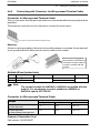
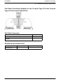
The FP2 uses the term “module” when express the size of the unit or backplane.
The unit installation sizes come in two sizes: the basic 1-module size, and the 2-module
size that is twice as wide.
The 1-module unit is the size that physically takes up the space of one guide on the
backplane.
The 2-module unit is the size that physically takes up the space of two guides on the
backplane.
1-module unit
2-module unit
Backplane Selection
Following two kinds of backplanes are available.
1) FP2 backplane (AFP25***) (Color of letters on the printed board: White)
2) FP2 backplane H type (AFP25****H) (Color of letters on the printed board: Yellow)
These two backplanes cannot be used in combination.
Carefully select the type of backplanes before you order.
The selection of the backplane should be based on the total number of modules to be
used in the system. In other words, the module number of the backplane must be
greater than or equal to the total number of modules for the system. So be sure to select
a backplane that allows the installation of all the required units.
ix
Table of Contents
FP2/FP2SH
When using the FP3, FP10SH, or Other Units
Backplane slot number
The backplane for the FP2 is specified by the total number of slots, i.e., 14-module type,
including the connectors for the power supply unit and CPU. The number of connectors
(or slots) remaining for the I/O units and intelligent units is then the module number of
the backplane minus the number of modules for the power supply unit and CPU.
Similarly, the number of connectors (or slots) remaining for the I/O units on expansion
backplanes is the module number of the backplane minus the number of modules for
the power supply unit.
Expansion backplanes
1. FP2 backplane
− Does not support expansion with 5-module type backplanes.
− Backplanes that are not the 5-module type can be used as expansion backplanes.
2. FP2 backplane H type
− This backplane is functionally equivalent to the backplane for FP3.
− There are the basic backplane H type for installing I/O units and the expansion
backplane H type for adding I/O units more.
− The basic backplane cannot be used as an expansion backplane.
Removal and Installation of Expansion Memory Unit
During removal and installation of expansion memory unit, the contents of the internal
RAM may be erased, so be sure to save a copy of the program and data onto a disk
before beginning the operations.
Use programming tool software (NPST−GR/FPWIN GR) for backup purposes.
Before rewriting the backed up program and data to the programmable controller, be
sure to clear the program in the programmable controller.
x
FP2/FP2SH
Table of Figures
With the FP2SH
Programming Tool Restrictions
The following tool software is required in order to program the FP2SH.
“FPWIN GR”
“NPST−GR” Ver. 4.6 or a subsequent version
Request Concerning Program Storage
To prevent the accidental loss of programs, the user should consider the following
measures.
Drafting of documents
To avoid accidentally losing programs, destroying files, or overwriting the contents of
a file, documents should be printed out and then saved. Disks should be organized to
assure safe maintenance.
Specifying the password carefully
The password setting is designed to avoid programs being accidentally overwritten. If
the password is forgotten, however, it will be impossible to overwrite the program even
if you want to. Also, if a password is forcibly bypassed, the program is deleted. When
specifying the password, note it in the specifications manual or in another safe location
in case it is forgotten at some point.
Saving programs to the ROM
In order to prevent programs from being lost if the backup battery runs down, and to
prevent accidental overwriting of programs in the workplace, we recommend saving
programs entered in the RAM to the ROM. If the PLC is used over a long period of time,
this concern applies particularly to programs that are built into the device when shipped.
Check the manuals for specifications and other items pertaining to usage.
FP series Programming Manual
xi
Table of Contents
FP2/FP2SH
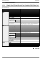
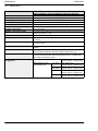
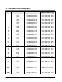
Compatibility with CPU unit, and Precautions
Comparison of Specifications
FP2 CPU
Items
Controllable I/O
points
Basic construction
Expanded
construction
Program capacity
Operation speed
(typical value)
Using remote I/O
system
Internal memory
FP2SH CPU
AFP
6221V3
Using Backplanes: Max. 768 points (12
modules)
Using Backplanes H type: Max. 512 points
(8 modules)
Using Backplanes: Max. 1,600 points (25
modules)
Using Backplanes H type: Max. 2,048
points (32 modules)
Max. 2,048 points
Max. 8,192 points
Max. 512 points
Approx. 16k steps
Approx. 30k steps
Approx. 32k steps
Approx. 60k steps
(For FP2−C3P,
approx. 120k steps)
—
From 0.35µs per
instruction
From 0.03µs per
instruction
High-level instructions From 0.93µs per
instruction
From 0.06µs per
instruction
Using expansion
memory
Basic instructions
FP10SH CPU
FP2−C1, FP2−C1D, FP2−C2L, FP2−C2,
FP2−C1A,FP2−C1SL FP2−C2P,FP2−C3P
AFP
6211V3
Max. 2,048 points
Max. 8,192 points
Approx. 60k steps/
120k steps
From
From
0.04µs per 0.10µs per
instruction instruction
From
From
0.08µs per 0.20µs per
instruction instruction
8,192 points
8,192 points
14,192 points
Total 3,072 points
10,240 points
2,048 points
2,048 points
10,240 words
32,765 words
Operation
p
Relays
y
memory
points
2,048 points
2,048 points
4,048 points
Total 1,024 points
2,048 points
1,024 points
None
6,000 words
0 to 14,333 words
(when expanding: 0
to 30,717 words)
8,192 points
8,192 points
14,192 points
Total 3,072 points
10,240 points
2,048 points
2,048 points
10,240 words
FP2−C2L: 32,765
words
FP2−C2, FP2−C2P,
FP2−C3P: 32,765
words × 3 banks
Link data registers
(LD)
Timer/counter set
value area (SV)
Timer/counter elapsed
value area (EV))
Index registers
(I0 to ID)
Comment input function
256 words
8,448 words
8,448 words
1,024 words
3,072 words
3,072 words
1,024 words
3,072 words
3,072 words
14 words
14 words×16 banks
14 words×16 banks
Optional function
Optional function
Clock/calendar function
Optional function
ROM operation function
Optional function
Built−in (Internal)
function
Built−in (Internal)
function
FP2−C2L, FP2−C2:
Optional function
FP2−C2P, FP2−C3P:
Built−in (Internal)
function
External input (X)
External output (Y)
Internal relays (R)
Timer/counter (T/C)
Link relays (L)
Pulse relays (P)
Alarm relays (E)
Memory Data registers (DT)
areas
File registers (FL)
xii
Built−in (Internal)
function
Optional function
FP2/FP2SH
Table of Figures
Compatibility of FP2SH and FP2, and
Precautions
Hardware Compatibility
Most of the units and related products used with the FP2SH can be used with the FP2,
but the following differences should be noted.
Some optional memory units cannot be used.
The only memory unit that can be used with the FP2SH CPU FP2−C2 or FP2−C2L” is
the ”Part number FP2−EM7 or Model number AFP2208”.
The FP2 memory units “Part numbers FP2−EM1, FP2−EM2, FP2−EM3, and
FP2−EM6” cannot be used.
The types of optional ROMs are different.
The only ROM that can be used with the FP2SH CPU unit ”FP2−C2” is the ”Model
number AFP5208 or AFP5209”. The nonvolatile memory implemented memory unit
”Model number AFP2208” can be also used.
The FP2 ROM “Part number AFP2204” and “Part number AFP2205” cannot be used.
The backup battery types are different.
The backup battery for the FP2SH CPU is the “Part number AFP8801” battery with a
connector.
The “Part number AFC8801” battery for the FP2 CPU cannot be used.
The calendar timer and comment memories have been installed in advance.
These have already been installed in the FP2SH CPU, and no optional units are
needed.
ROM operation functions in the FP2SH
CPUs that support IC memory cards (FP2−C2P and FP2−C3P) have an internal FROM
used as a program memory. The internal FROM cannot be replaced.
Software Compatibility
The FP2SH has a higher level of compatibility than the FP2, so there are no functions
that cannot be used with the FP2SH. Other factors, such as the number of device
points, should be confirmed by checking the specifications comparison table on the
previous page.
xiii
Table of Contents
FP2/FP2SH
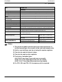
IC memory cards for the FP2SH
The existing model number becomes the one to be discontinued because of the
termination of manufacturing IC memory cards by the parts manufacturer. When placing
a new order, specify the new product number.
Termination of Production
Type
SRAM
Memory capacity
2MB
Model No.
Battery type
AIC52000
Internal secondary battery (Rechargeable type)
Model No.
Battery type
AFP2209
Lithium Battery (Interchangeable type)
New product
Type
SRAM
Memory capacity
2MB
Notes
For AFP2209
• An interchangeable lithium battery is used. When you use for
the first time, install the battery included.
For AIC52000
• Memory backup of the SRAM type of IC memory card
(AIC52000) Is handled by an internal secondary battery. When
the battery is used for the first time, power must be supplied
for at least 24 hours to charge it fully. When the battery is fully
charged, data is backed up for more than three months with
out the power being turned on. Normally, the card should be
installed in the PLC and power supplied when using it. Failing
to charge the battery periodically can reduce the backup
period and the service life of the battery. The backup battery
cannot be replaced.
xiv
FP2/FP2SH
Table of Figures
Compatibility of FP2/FP2SH and FP10SH,
and Precautions
Hardware Compatibility
The unit, backplane, and other components are not compatible.
The components for the FP2 are used with the FP2SH.
When using the FP2 backplane (AFP25**), the maximum number of expansion
points is lower.
With the FP10SH and FP2 backplane H type (AFP25**H), up to three expansion boards
can be used, and a maximum of 2048 points controlled, but if using the FP2 backplane
with the FP2/FP2SH, only one expansion board can be used, and a maximum of 1600
points controlled.
Different types of IC memory cards are used.
The only type of IC card that can be used with the “Part number FP2−C2P and
FP2−C3P” FP2SH CPU is the IC memory card (small PC card). The IC memory card
for the FP10SH cannot be used.
Software Compatibility
With the FP2SH, in comparison with the FP10SH, there are no functions that cannot
be used. For other detailed specifications, check the specifications comparison table
on the previous page.
xv
Table of Contents
FP2/FP2SH
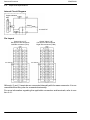
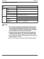
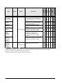
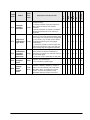
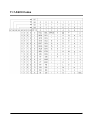
Programming Tool Restrictions
Restrictions on usable programming tools depending on the units
Type of unit
Type
yp of p
programming
g
g tool
FP2
Windows software
AFP1113V2
Used
Note 3)
Not used
AFP1114V2
AFP1113
Not used
Not used
Not used
Not used
Used
Used
FPWIN GR Ver.1
Windows software
Conforms to
IEC61131 3
IEC61131−3
FPWIN Pro Ver.6
Handy programming
unit
FPWIN Pro Ver.5
Used
Note 1)
Used
Note 1)
Used
FP2SH
Used
Note 1)
Used
Note 1)
Used
Note 2)
Used
Note 3)
Not used
FPWIN GR Ver.2
AFP1114
AFP1111A
AFP1112A
AFP1111
AFP1112
FP Memory Loader
AFP8670
AFP8671
Note 4)
Note 1) FPWIN GR Ver.2.91 or later version is necessary to use the FP2SH CPU (32k type).
FPWIN GR Ver.2.40 or later version is necessary to use the multi communication unit.
FPWIN GR Ver.2.71 or later version is necessary to use the MEWNET−VE Link Unit.
The FNS Unit and FMU Unit cannot use to FPWIN GR.
Note 2) FPWIN Pro Ver.6.3 or later version is necessary to use the FP2SH CPU (32k type).
Note 3) FPWIN Pro Ver.5.02 or later version is necessary to use the multi communication unit.
−FPWIN Pro Ver.5.24 or later version is necessary to use the MEWNET−VE Link Unit.
−FPWIN Pro Ver.5.24 or later version is necessary to use the FNS Unit.
−FPWIN Pro Ver.5.3 or later version is necessary to use the FMU Unit.
Note 4) FP Memory Loader Ver.2.1 or later version is necessary to use the FP2SH CPU (32k
type). When using FP2SH CPU (120k type), only the 1st program and comments can
be transferred.
Note: Precautions concerning version upgrade
• In case of using FPWIN GR Ver.1, please purchase upgrade model
FPWIN GR Ver.2.
• FPWIN GR Ver. 2.0 can be upgraded to Ver. 2.1 or later free of
charge at our web site.
• FPWIN Pro Ver. 6.0 can be upgraded to Ver. 6.1 or later free of
charge at our web site
(http://industrial.panasonic.com/ac/e/dl_center/software/).
xvi
Chapter 1
Overview
Overview
1−2
FP2/FP2SH
FP2/FP2SH
Overview
1.1
1.1
1.1.1
System Configuration
System Configuration
Basic Configuration by Number of Slots
The building block scheme allows you to combine units as desired.
Five types of backplanes and Two types of backplanes H types are available for the
FP2/FP2SH. A variety of input/output units can be installed as desired on the backplane.
Although most of the I/O units and intelligent units can be combined freely in the layout,
you should check the following three points when selecting your units:
− Restrictions on unit types
section 1.2.2.1
− Limitations on the internal current consumption
section 1.2.2.2
− Limitations on the number of modules of the backplane
page 1 − 4
FP2 backplane
5 modules
7 modules
9 modules
12 modules
14 modules
FP2 backplane H type
Basic backplane (11 modules)
Expansion backplane (10 modules)
Following two kinds of backplanes are available.
1) FP2 backplane (AFP25***)
2) FP2 backplane H type (AFP25****H)
These two backplanes cannot be used in combination.
Carefully select the type of backplanes before you order.
1−3
Overview
1.1
FP2/FP2SH
System Configuration
Restriction on the number of modules of the backplane (For master backplane)
The number of units that can be installed is determined by the number of modules of
the backplane used, the power supply unit to be installed, and the CPU.
1 module type CPU
Standard type CPU
2 modules type CPU
CPU with 64-point input, CPU with S-LINK
1 module type power supply unit
100V 2.5A, 200V 2.5A
2 modules type power supply unit
100 to 240V 5A, 24V DC 5A
CPU backplane
FP2 backplane
5-module type
1 module type
CPU and
1 module type
power supply
unit
2 modules type
CPU and
1 module type
power supply
unit
1 module type
CPU and
2 module type
power supply
unit
2 modules type
CPU and
2 module type
power supply
unit
7-module type 9-module type
14-module type
3 slots free
5 slots free
7 slots free
10 slots free
12 slots free
2 slots free
4 slots free
6 slots free
9 slots free
11 slots free
2 slots free
4 slots free
6 slots free
9 slots free
11 slots free
1 slot free
3 slots free
5 slots free
8 slots free
10 slots free
* slots free: Number of slots where units can be installed
1−4
12-module type
FP2/FP2SH
Overview
1.1
System Configuration
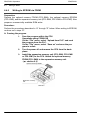
FP2 backplane H type
11−module type
1 module type
CPU and
1 module type
power supply
unit
8 slots free
2 module type
CPU and
1 module type
power supply
unit
7 slots free
1 module type
CPU and
2 module type
power supply
unit
8 slots free
2 module type
CPU and
2 module type
power supply
unit
7 slots free
1.1.2
A maximum of eight I/O units (including the unit built in the CPU)
can be controlled per backplane. Even if further I/O units are
installed, they are not recognized.
Note) When using the CPU unit with S−LINK, seven slots are free,
however, the units actually usable are only six. (Refer to Chapter 3
I/O Allocation.)
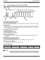
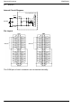
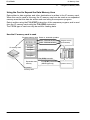
Expansion of Backplane
FP2 backplane
CPU backplane
Expansion backplane
Expansion cable
Only one backplane can be added-on for expansion.
Expansion is simply connecting a new backplane with a special expansion cable. Any
backplane other than a 5-module type can be used for expansion.
Notes
•
•
•
•
A 5-module type backplane cannot be expanded.
A 5-module type backplane cannot be added on for expansion.
Only one backplane can be added-on for expansion.
A power supply unit is also necessary on an expansion backplane.
next page
1−5
Overview
1.1
FP2/FP2SH
System Configuration
•
•
Do not install a CPU on an expansion backplane.
There is no need to make the number of modules on the expansion backplane equal to the number of modules on the
CPU backplane.
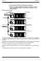
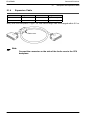
FP2 backplane H type
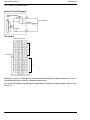
CPU unit
Power supply unit
Basic backplane
I/O unit
Backup battery
Expansion memory
Expansion cable
Power supply unit
Board No. setting
switches
COM port
Tool port
I/O unit
Expansion backplane 1
Expansion backplane 2
Expansion backplane 3
The basic FP2 backplane H type that the CPU unit can be installed and the expansion
backplane H type that only the I/O units and the intelligent I/O units can be installed are
available.
A maximum of eight I/O units (including the unit built in the CPU) can be controlled per
backplane. Even if further I/O units are installed, they are not recognized.
Up to three expansion backplanes can be added on for expansion.
Use the board No. setting switches on the board to distinguish the expansion backplane.
A power supply unit is also necessary on an expansion backplane.
1−6
FP2/FP2SH
Overview
1.1
System Configuration
Restriction on the number of modules of the backplane (For expansion backplane)
The number of units that can be installed is determined by the number of modules of
the backplane used and the power supply unit to be installed.
FP2 backplane
7-module type
1 module type
power supply
unit
2 module type
power supply
unit
9-module type
12-module type
14-module type
6 slots free
8 slots free
11 slots free
13 slots free
5 slots free
7 slots free
10 slots free
12 slots free
* slots free: Number of slots where units can be installed
FP2 backplane H type
10-module type
1 module type
power supply
unit
8 slots free
2 module type
power supply
unit
8 slots free
Note) Although the connectors for installing I/O units are free with a 1−module type power supply unit, they cannot be used.
Expansion cable
Order number
Length
Ferrite core
FP2−EC
60 cm
1
FP2−EC2
2m
2
Note) With the backplalne H type, the total cable length can be arranged within 3.2 m.
1−7
Overview
1.2
FP2/FP2SH
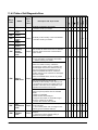
Unit Types and Combinations
1.2
Unit Types and Combinations
1.2.1
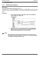
Line-Up of Backplanes and Units
Power supply units
Backplanes
100V AC 2.5A type
(FP2−PSA1)
100 to 240V AC 5A type
(FP2−PSA3)
200V AC 2.5A type
(FP2−PSA2)
24V DC 5A type
(FP2−PSD2)
FP2 CPU
FP2SH CPU
(for CPU and expansion backplanes)
The 5−module type
backplane can not be
used for expansion.
5-module type
(FP2−BP05)
7-module type
(FP2−BP07)
Standard type
CPU
(FP2−C1)
CPU with
64-point input
(FP2−C1D)
CPU with
S-LINK
(FP2−C1SL)
(FP2−BP09)
FP2−EM3
FP2−EM6
FP2−EM7
Type of memory unit
Part No.
Comment Clock/
With 16k ROM
input
calendar expansion socket
function function RAM
FP2−EM1
A
A
N/A
N/A
12-module type
FP2−EM2
A
A
A
N/A
(FP2−BP12)
FP2−EM3
A
A
A
A
FP2−EM6
N/A
N/A
A
A
FP2−EM7
N/A
N/A
N/A
A
14-module type
A: Available, N/A: Not available
(FP2−BP14)
Backplanes H type
FROM FP2−EM4
FP2−BP11MH (AFP25011MH)
10-module type (Expansion)
FP2−BP10EH (AFP25010EH)
1−8
Memory unit
ROM socket
(FP2-EM7)
F−ROM EP−ROM
(AFP5208)(AFP5209)
Memory unit for FP2SH
Memory unit F−ROM implemented)
(AFP2208)
Small PC card for FP2SH
EPROM FP2−EM5
Option
11-module type (Basic)
Small PC card compliant type:
60k step: FP2−C2P
(AFP2235)
120k step: FP2−C3P
(AFP2255)
Memory unit for FP2SH
Optional memories
For FP2
FP2−EM1
FP2−EM2
9-module type
Standard type:
32k step: FP2−C2L
(AFP2221)
60k step: FP2−C2
(AFP2231)
Product name
Product number
Dummy unit
AFP2300
Battery
atte y
Lithium battery (button)
AFC8801
Lithium battery
AFP8801
Battery for AFP2209
AFP2806
Terminal block for FP2 I/O unit
AFP2800
Set of connector for wire−pressed
AFP2801
terminal cable (2 pieces)
Set of flat cable connector (2 pieces)
AFP2802
FROM type IC memory card
(AIC50020)
SmallSRAM
SRAM type IC
memory card
(AIC52000)
Discontinued
products
SmallSRAM
SRAM type IC
memory card
(AFP2209)
FP2/FP2SH
Overview
1.2
Unit Types and Combinations
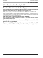
Input, Output and I/O mixed units
16-point DC input
(FP2−X16D2)
16-point transistor output
NPN type (FP2−Y16T)
16-point transistor output
PNP type (FP2−Y16P)
6-point relay output type
(FP2−Y6R)
16-point relay output type
(FP2−Y16R)
32-point DC input
(FP2−X32D2)
32-point transistor output NPN type
(FP2−Y32T)
32-point transistor output PNP type
(FP2−Y32P)
64-point DC input (FP2−X64D2)
64-point transistor output NPN type
(FP2−Y64T)
64-point transistor output PNP type
(FP2−Y64P)
32-point input/ 32-point output
NPN type (FP2−XY64D2T)
32-point input/output (NPN) with on
pulse catch input (FP2−XY64D7T)
32-point input/ 32-point output
PNP type (FP2−XY64D2P)
32-point input/output (PNP) with on
pulse catch input (FP2−XY64D7P)
DA4
Analog input
FP2−AD8VI
Positioning
(2−axis)
FP2−PP2
Analog output
FP2−AD8X
Positioning
(4−axis)
FP2−PP4
Analog output
FP2−DA4
Positioning (2−axis)
Multifunction
Transistor FP2−PP21
Line driver FP2−PP22
Serial data
FP2−SDU
C.C.U
FP2−CCU
Multi−wire link
FP2−MW
Remote I/O Slave
FP2−RMS
FMU
FP2−DPV1−M
RTD input
FP2−RTD
FMU
FP2−DEV−M
Positioning (4−axis)
Multifunction
Transistor FP2−PP41
Line driver FP2−PP42
MCU
FP2−MCU
S-LINK
FP2−SL2
Communication
Block
FP2−CB232
FP2−CB422
MEWNET−VE link
FP2−VE
FMU
FP2−CAN−M
FNS
FP2−FNS
High speed counter
FP2−HSCT(NPN)
FP2−HSCP(PNP)
Positioning RTEX
FP2−PN2AN
(2−axis)
FP2−PN4AN
(4−axis)
FP2−PN8AN
(8−axis)
Pulse I/O
FP2−PXYT(NPN)
FP2−PXYP(PNP)
Positioning (2−axis)
(Interpolation)
Transistor FP2−PP2T
Line driver
FP2−PP2L
Positioning (4−axis)
(Interpolation)
Transistor FP2−PP4T
Line driver FP2−PP4L
Communication
Block
FP2−CB485
MEWNET−VE2 link
FP2−VE2
Communication
Block
PROFIBUS
(AFPN−AB6200)
ET−LAN
FP2−ET1
Communication
Block
DeviceNet
(AFPN−AB6201)
ET−LAN2
FP2−ET2
Communication
Block
CANopen
(AFPN−AB6218)
1−9
Overview
1.2
FP2/FP2SH
Unit Types and Combinations
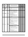
1.2.2
Combinations That Can be Used and Restrictions
1.2.2.1
Restrictions on Unit Types
Backplanes and
units used
System
configuration
Backplane
Backplane
H type
(5module
type)
(7-, 9-,
12-, 14module
type)
Basic
(11−
module
type)
Expansion
(10−
module
type)
A
A
A
N/A
N/A
A
N/A
A
A
A
A
Power
supply
pp y
unit
CPU
unit
Remote
I/O
slave
unit
Input
unit
Output
unit
I/O
mixed
unit
A
A
N/A
A
A
A
A
*4
A
N/A
N/A
A
A
A
A
N/A
A
N/A
A
A
A
A
A
A
A
N/A
N/A
A
A
A
CPU backplane
Install in order from the left to the right, the
power supply unit, the CPU unit, the I/O and
the intelligent units.
Expansion backplane
Install in order from the left to the right, the
power supply unit, the I/O and the intelligent
units.
Slave station
system backplane
ne
Master backplane for slave station
system
Install in order from the left to the right,
the power supply unit, the Remote I/O
slave unit,the I/O and the intelligent
units.*Replace the CPU on the CPU
backplane with a remote I/O slave unit.
Expansion backplane for slave
station system
Install in order from the left to the right,
the power supply unit, the I/O and the
intelligent units.* Same as the installation of the expansion backplane.
Limitations on Combining Link Units
Unit type and mode
When CPU unit is FP2
When CPU unit is FP2SH
Computer communication unit
Only one unit (see note)
Multi−wire Link unit
(MEWNET
W mode)
(MEWNET−W
Can be installed within 3 units in combination
with W link, CCU and MCU (PC link mode).
Can be installed within 5 units in combination
with
ith W link,
li k CCU and
d MCU (PC link
li k mode).
d )
Can be installed within 2 units in combination with MCU in PC (PLC) link mode.
Multi−wire Link unit
(MEWNET−W2 mode)
ET−LAN unit
Up to 3 units can be used.
Up to 2 units out of 3, when including PC
(PLC) link.
Up to 8 units can be used.
Up to 2 units out of 8, when including PC
(PLC) link.
Multi Communication unit
(PC (PLC) link mode)
Can be installed within 3 units in combination
with W link, CCU and MCU.
Can be installed within 5 units in combination
with W link, CCU and MCU.
Can be installed within 2 units in combination with W link unit in PC (PLC) link mode.
Multi Communication unit
(Computer link mode)
Up to 8 units can be used.
MEWNET−VE Link Unit
Not Available
Can be installed within 2 units in combination
with Multi Communication Unit.
Note
Depending on the location of the connected ports and the commands used for communication, up to 3 units can be used. For
more details, refer to the Computer Communication Unit Manual.
1 − 10
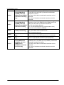
FP2/FP2SH
Overview
1.2
Output
unit
I/O
mixed
unit
Analog
input
unit
Analog
output
unit
A
A
A
A
A
A
A
A
A
A
N/
A
N/
A
A
A
N/
A
N/
A
High
−
spe
p
ed
cou
nter
unit
Pulse
I/O
unit
A
A
*1
*1
A
A
*1
*1
*5
*5
Positioning
unit
(PP2
/PP4)
Positioning
unit
(Multi−
function
type)
Positioning
unit
RTEX
Positioning
unit
Interpolation
type
Serial
data
unit
A
A
A
A
A
A
A
A
A
A
N//
A
N/
A
N/
A
N/
A
A
N//
A
N/
A
N/
A
N/
A
A
N//
A
A
A
A
*6
*6
*7
A
A
A
*6
*6
*7
Computer
communication
unit
A
*2
S−
LINK
unit
Multi−wire link unit
MEWNET−
F
mode
A
A
A
*8
A
*8
Unit Types and Combinations
MEWNET−
W
mode
ET−
LAN
unit
MEWNET−
W2
mode
Multi
communication
ME
WNET
−VE
VE
Link
Unit
FNS
unit
FMU
unit
A
A
A
A
A
A
A
A
*3
*2
*2
*2
*2
*2
A
N/
A
N/
A
N/
A
A
*3
*2
N/
A
A
A
N/
A
N/
A
N/
A
N/
A
N/
A
N/
A
N/
A
N/
A
N/
A
N/
A
N/
A
N/
A
N/
A
N/
A
N/
A
N/
A
A: Available N/A: Not available
Notes
1) When “Mode B: Unit with interrupt function” has been specified, the unit will be treated as interrupt unit, and 8 interrupts
per unit will be available for use. However, when “Mode B” has
been set for the unit, 2 units can be used with 1 CPU unit.
When “Mode C: Intelligent unit that generate interrupts” has
been specified, and 1 interrupt per unit will be available for
use. However, when “Mode C” has been set for the unit, 8
units can be used with 1 CPU unit.
2) Check the limitations on combining link units given below.
3) In the MEWNET−F mode, up to four units can be used counting
the CPU and expansion sides.
4) With the backplane H type, the total expansion cable length
can be arranged within 3.2 m.
5) The unit cannot be installed on the 31st slot (last slot) when
using the H−type backplane.
6) The interrupt function is not available for the backplane on the
slave station system.
7) With the backplane on the slave station system, the time taken
from the startup until the completion of positioning should be
longer than a scan time.
8) With the backplane on the slave station system, I/O points
cannot be set including 96 input points and 96 output points.
1 − 11
Overview
1.2
FP2/FP2SH
Unit Types and Combinations
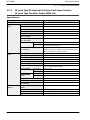
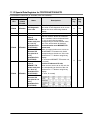
1.2.2.2
Limitations on Current Consumption
Internal supply power (5V)
passes through the bus of
the backplane to each unit.
Power supply unit
Rated current (at 5V)
FP2−PSA1
2.5A
FP2−PSA2
2.5A
FP2−PSA3
5A
FP2−PSD2
5A
Power goes from a commercially available
power supply to each I/O unit.
Commercially
available
power supply
24V
Internal supply power (5V DC)
The 5V DC power used for driving the internal circuit of each unit is supplied from the
power supply unit through the internal bus of the backplane.
External supply power (24V DC)
The 24V DC power supply used as the input power supply of the input units and the
output circuit driving power of the output units are supplied from the external terminal
of each unit.
For 24V power supply, commercially available power supply equipment is used.
Combining units and selecting a backplane
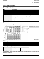
The current consumed by each unit is shown in the following pages.
Give consideration to the combination of units so that the rated capacity of 5V DC and
24V DC power supplies should not exceeded.
Example of current consumption calculation
The table below shows the combination of typical units on a 9-module type backplane.
Type
Number of units and
backplane used
Current consumption at
5V DC (mA)
Current consumption at
24V DC (mA)
CPU (FP2−C1)
1
410
0
Backplane (FP2−BP09)
1
60
0
Input unit (FP2−X16D2)
3
60×3=180
8×16×3 = 384
Output unit (FP2−Y16R)
4
120×4=480
160×4=640
1130
1024
Total current consumption
1 − 12
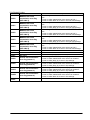
FP2/FP2SH
Overview
1.2
Unit Types and Combinations
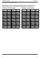
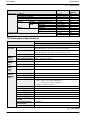
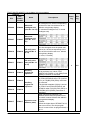
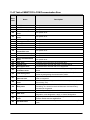
Table of current consumption at 5V DC
Type
Part number
Current consumption at
5V DC (mA)
FP2 CPU
FP2−C1
410 or less
FP2−C1D
530 or less
FP2−C1SL
630 or less
FP2−C1A
1060 or less
FP2−C2L
750 or less
FP2−C2
750 or less
FP2−C2P
750 or less
FP2−C3P
750 or less
FP2−BP05
5 or less
FP2−BP07
60 or less
FP2−BP09
60 or less
FP2−BP12
60 or less
FP2−BP14
60 or less
FP2−BP11MH
5 or less
FP2−BP10EH
60 or less
16-point terminal type, 12 to 24V DC
FP2−X16D2
60 or less
32-point connector type, 24V DC
FP2−X32D2
80 or less
64-point connector type, 24V DC
FP2−X64D2
100 or less
Relay
e ay outout
putt
6-point terminal type
FP2−Y6R
50 or less
16-point terminal type
FP2−Y16R
120 or less
Transistor
a s sto
output
t t
16-point terminal NPN type
FP2−Y16T
100 or less
32-point connector NPN type
FP2−Y32T
130 or less
64-point connector NPN type
FP2−Y64T
210 or less
16-point terminal PNP type
FP2−Y16P
80 or less
32-point connector PNP type
FP2−Y32P
130 or less
64-point connector PNP type
FP2−Y64P
210 or less
FP2SH CPU
Backplane
Backplane
ac p a e H type
Input
put u
unitt
Output
unit
it
DC
C input
put
I/O
/O mixed
ed
unit
it
32-point 24V DC input/32-point connector NPN output type FP2−XY64D2T, FP2−XY64D7T
160 or less
32-point 24V DC input/32-point connector PNP output type FP2−XY64D2P, FP2−XY64D7P
160 or less
Intelligent
te ge t
unit
it
Analog input unit (Voltage/current type)
FP2−AD8VI
400 or less
Analog input unit (Channel type)
FP2−AD8X
300 or less
RTD input unit
Analog output unit
FP2−RTD
FP2−DA4
300 or less
600 or less
High speed
High−speed
counter
t unit
it
NPN
FP2−HSCT
450 or less
PNP
FP2−HSCP
450 or less
Pulse I/O
unit
it
NPN
FP2−PXYT
500 or less
PNP
FP2−PXYP
500 or less
Positioning
os t o g
unit
it
2-axis type
FP2−PP2
225 or less
4-axis type
FP2−PP4
400 or less
Positioning
os t o g
unit
it (M
(Multilti
function
type)
2-axis
a s
t
type
Transistor output type
FP2−PP21
200 or less
Line driver output type
FP2−PP22
200 or less
4-axis
a s
t
type
Transistor output type
FP2−PP41
350 or less
Line driver output type
FP2−PP42
350 or less
2-axis type
FP2−PN2AN
300 or less
4-axis type
FP2−PN4AN
300 or less
8-axis type
FP2−PN8AN
300 or less
Positioning
os t o g
unit
it RTEX
2-axis
a s
t
type
Transistor output type
FP2−PP2T
300 or less
Line driver output type
FP2−PP2L
300 or less
4-axis
a s
t
type
Transistor output type
FP2−PP4T
300 or less
Line driver output type
FP2−PP4L
300 or less
Serial data unit
FP2−SDU
60 or less
Multi communication unit
with Communication block (1−unit or 2−unit)
FP2−MCU
480 or less
Positioning
os t o g
unit
it (I
(Intert
polation
type)
next page
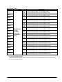
1 − 13
Overview
1.2
FP2/FP2SH
Unit Types and Combinations
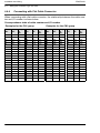
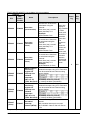
Type
Intelligent
unit
it
Part number
Current consumption at
5V DC (mA)
C.C.U.
FP2−CCU
60 or less
S-LINK unit
FP2−SL2
130 or less
Multi-wire link unit
FP2−MW
220 or less
Remote I/O Slave Unit
FP2−RMS
150 or less
ET−LAN unit
FP2−ET1
670 or less
MEWNET−VE Link unit
FP2−VE
670 or less
FP2−FNS
55 or less
PROFIBUS
AFPN−AB6200
230 or less
Device Net
AFPN−AB6201
65 or less
CAN open
AFPN−AB6218
65 or less
PROFIBUS
FP2−DPV1−M
450 or less
Device Net
FP2−DEV−M
150 or less
CAN open
FP2−CAN−M
450 or less
FNS unit
FNS unit
FP FNS
FP−FNS
Bl k
Block
FMU unit
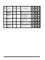
Table of current consumption at 24V DC
Type
Input
put u
unitt
Output u
unitt
Part number
Current consumption at
24V DC (mA)
16-point terminal type, 12 to 24V DC
FP2−X16D2
8 or less per one point
32-point connector type, 24V DC
FP2−X32D2
4.3 or less per one point
64-point connector type, 24V DC
FP2−X64D2
4.3 or less per one point
6-point terminal type
FP2−Y6R
70 or less
16-point terminal type
FP2−Y16R
160 or less
16-point terminal NPN type
FP2−Y16T
120 or less
32-point connector NPN type
FP2−Y32T
140 or less
64-point connector NPN type
FP2−Y64T
250 or less
16-point terminal PNP type
FP2−Y16P
70 or less
32-point connector PNP type
FP2−Y32P
150 or less
64-point connector PNP type
FP2−Y64P
270 or less
3 po t 24V DC
32-point
C input/32-point
put/3 po t co
connector
ecto NPN
output
t t ttype
FP2−XY64D2T,
6
,
FP2 XY64D7T
FP2−XY64D7T
Input: 4.3 or less per one point
32-point 24V DC input/32-point connector PNP
output type
FP2−XY64D2P,
FP2−XY64D7P
FP2
XY64D7P
Input: 4.3 or less per one point
DC
C input
put
Relay
e ay output
Transistor
a s sto
output
t t
I/O
/O mixed
ed u
unitt
Output: 120 or less
Output: 130 or less
Notes
•
•
1 − 14
The input unit displays the current flowing to the internal circuit. The other units display the current value required to drive
the internal circuit. This value does not include the load current of the output unit.
Refer to the manual of the particular unit you are using to
confirm the current consumed at 24V by the S-LINK units,
Positioning units, High−speed counter units and Pulse I/O
units.
FP2/FP2SH
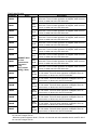
Overview
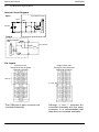
1.3
1.3
1.3.1
Expansion Function
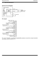
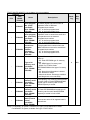
Computer Link
1:1 communication
The FP2 CPU can be directly
connected to a computer through
the COM (RS232C) port.
PC
Expansion Function
1:N communication
A C-NET adapter can be used to enable
communication for a number of programmable
controllers.
PC
C-NET adapter
(AFP8536/AFP8532)
FP2/FP2SH
Commercially available RS232C cable
FP2/FP2SH
COM port
S2 type
Commercially available
RS232C cable
FP2/FP2SH
Two-core cable (RS485)
(VCTF0.75 × 2C)
S2 type
A maximum of 32 stations can be connected.
Since a COM (RS232C) port and TOOL (RS232C) port comes standard on the CPU for
the FP2/FP2SH, direct communication with the computer can be achieved without the
addition of any intelligent units.
Using a host computer program, the relay conditions and register contents of the CPU
can be read and written.
With communications from a host computer, communication programs are unnecessary
on the CPU side.
1 − 15
Overview
1.3
FP2/FP2SH
Expansion Function
Table of specifications
Item
Description
1:1 communication
1:N communication
Communication method
Half duplex
Half duplex
Synchronization method
Start−stop synchronous system
Communication path
RS232C cable
Two-core cable
(VCTF 0.75mm2 × 2C)
Transmission distance
Max. 15m/49.2ft.
Max. 1200m/3,937ft.
Transmission speed
(Baud rate)
1200bps/2400bps/4800bps/9600bps/
19200bps/38400bps/57600bps/115.2Kbps
9600bps/19200bps
Transmission code
ASCII
Transmission format
Stop bit: 1 bit/2 bits
Parity check: none/even/odd
Character bits: 7 bits/8 bits
Necessary devices in configuration
1:1 communication
1:N communication
FP2/FP2SH
FP2/FP2SH
Commercially available computer
Commercially available computer
Commercially available RS232C cable
(AFB85813/AFB85853 or equivalent)
Commercially available RS232C cable
(AFB85813/AFB85853 or equivalent)
C-NET adapter (AFP8536/AFP8532) × 1 piece
C-NET adapter S2 type (AFP15402) × number of PLC
Two-core cable (VCTF 0.75mm2)
1 − 16
FP2/FP2SH
Overview
1.3
1.3.2
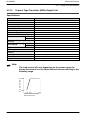
Connection of MODEM
1:1 communication
Connections to a MODEM can be
made using the COM port.
1:N communication
Using the C-NET adapter enables MODEMs to be
connected for multiple programmable controller.
MODEM
MODEM
MODEM
MODEM
Public line
Public line
Commercially available
RS232C cable
Commercially available
RS232C cable
FP2/FP2SH
PC
Expansion Function
PC
COM port
S2 type
C-NET adapter
(AFP8536/AFP8532)
FP2/FP2SH
Two-core cable (RS485)
(VCTF0.75 × 2C)
S2 type
FP2/FP2SH
A maximum of 32 stations can be connected.
The CPU of the FP2/FP2SH includes a COM (RS232C) port and TOOL (RS232C)
port as standard equipment, making it possible to connect a MODEM to perform programming and computer linking from a remote location using a public telephone line.
When the power supply of FP2/FP2SH is turned on, it will verify whether a MODEM is
connected, and, if a MODEM is, it will automatically transmit the AT command to set the
MODEM for automatic reception.
Since the reading and writing of the relay conditions and register contents of the programmable controller can be performed from the host computer, this function is
applicable for remote monitoring systems.
When using the TOOL port, you can use programming tool software (NPST-GR/FPWIN
GR) and perform reading and writing of the programmable controller program and maintenance operations via MODEM.
During 1:1 communication using the COM port, an error alarm can be issued from the
programmable controller.
1 − 17
Overview
1.3
FP2/FP2SH
Expansion Function
Table of specifications
Item
Description
1:1 communication
1:N communication
Communication method
Half duplex
Synchronization method
Start−stop synchronous system
Transmission speed
(Baud rate)
2,400bps/4,800bps/9,600bps/19,200 9,600bps/19,200bps
bps
Transmission code
ASCII
Transmission format
Character bit: 7 bits, parity check: odd and stop bit: 1 bit
Character bit: 8 bits, parity check: none and stop bit: 1 bit
Necessary devices in configuration
1:1 communication
1:N communication
FP2/FP2SH
FP2/FP2SH
Commercially available computer
Commercially available computer
MODEM
MODEM
Commercially available RS232C cable
Commercially available RS232C cable
* When using the TOOL port, an FP PC cable M5
type (AFC8513) and a self-made cable are necessary.
C-NET adapter (AFP8536/AFP8532) × 1 piece
1 − 18
C-NET adapter S2 type (AFP15402) × number of PLC
Two-core cable (VCTF 0.75mm2)
FP2/FP2SH
Overview
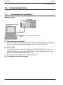
1.4
1.4
Programming Tools
Programming Tools
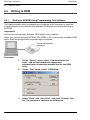
1.4.1
Tools Needed for Programming
Necessary tools
FP2/FP2SH
3
Commercially available
computer
2
Install
1
Programming tool software
1
Programming tool software
This is a program editing, debugging and document creating software package
that can be used with all programmable controllers in the FP series.
2
FP PC cable
This cable needed for connection between the FP2/FP2SH and the computer.
When connecting to a computer (IBM PC/AT or 100% compatible), use a comsection 1.4.2 )
mercially available adapter.(
For the following, use commercially available products.
3
Commercially available computer
1 − 19
Overview
1.4
1.4.2
FP2/FP2SH
Programming Tools
Software Environment and Suitable Cable
Standard ladder diagram tool software FPWIN−GR Ver.2
Type of software
OS
Hard disk capacity
Product No.
40MB or more
AFPS10520
(Operating system)
FPWIN GR Ver. 2
English−language
menu
Full type
Upgraded version
Windows 98
Windows Me
Windows 2000
Windows XP
Windows Vista
AFPS10520R
Note
1) Ver.1.1 must be installed to install the upgrade version.
2) Ver.2.0 can be upgraded to Ver. 2.1 or later free of charge at
our web site (http://industrial.panasonic.com/ac/e/dl_center/
software/).
Conforms to IEC61131−3 programming tool software FPWIN−Pro Ver.6
Type of software
OS
Hard disk capacity
Product No.
100MB or more
AFPS50560
(Operating system)
FPWIN GR Ver. 6 English−language menu
Windows 2000
Windows XP
Windows Vista
Note
1) The upgrade version is not available for Ver.6.
2) Ver.6.0 can be upgraded to Ver. 6.1 or later free of charge at
our web site (http://industrial.panasonic.com/ac/e/dl_center/
software/).
Type of computer and suitable cable
For the connection between a computer (RS232C) and the control unit (RS232C)
D−sub connector cable
PC side connector
PLC side connector
Specifications
Product No.
D−sub 9−pin
p
Mini DIN round 5−pin
L type (3 m)
AFC8503
Mini DIN round 5−pin
Straight type (3 m)
AFC8503S
Note
A USB/RS232C conversion cable is necessary to connect with a
personal computer without a RS232C port using a PC connection
cable.
1 − 20
FP2/FP2SH
Overview
1.4
1.4.3
Programming Tools
Tools Needed for ROM Creating
When Creating ROM with a Commercially Available ROM Writer with Optional Memory (FROM)
Necessary tools
1
Programming tool software and cable (
section 1.4.1)
Use a commercially available computer installed with the programming tool software and an FP PC cable.
2
Optional memory FROM
For FP2, FP2-EM4 (SST−29EE010−120−4C−PH or equivalent, SILICOM STORAGE TECHNOLOGY, INC.)
For FP2SH, AFP5208 (SST−29EE020−150−4C−PH or equivalent, SILICOM
STORAGE TECHNOLOGY, INC.)
3
Optional memory EPROM
For FP2, FP2-EM5 (M27C1001−12F1 or equivalent, SGS−THOMSON MICROELECTRONICS)
For FP2SH, AFP5209 (M27C2001−150F1 or equivalent, SGS−THOMSON MICROELECTRONICS)
For the following, use commercially available products.
4
Commercially available ROM writer
A ROM writer than can be used with memories
2
and
3
.
Note
1) The above explanation describes the case where the memory
unit is used in combination with the F−ROM and EP−ROM. As
the nonvolatile memory has been implemented in the memory
unit (Model number AFP2208), a commercial ROM writer cannot be used for writing.
2) The parts for the optional memory to be used differ depending
on FP2 or FP2SH.
1 − 21
Overview
1.4
FP2/FP2SH
Programming Tools
When Creating ROM with Programming Tool Software and a Commercially
Available ROM Writer
Necessary tools
1
Programming tool software (
section 1.4.1)
Use a commercially available PC installed with the programming tool software.
2
Optional memory EPROM
For FP2, FP2-EM5 (M27C1001−12F1 or equivalent, SGS−THOMSON MICROELECTRONICS)
For FP2SH, AFP5209 (M27C2001−150F1 or equivalent, SGS−THOMSON MICROELECTRONICS)
For the following, use commercially available products.
3
4
Commercially available ROM writer
A ROM writer than can be used with memory
2
.
Commercially available centronics cable or commercially available
RS232C cable
Use a cable that conforms with the specifications of the ROM writer.
Note
1) The above explanation describes the case where the memory
unit is used in combination with the EP−ROM. As the nonvolatile memory has been implemented in the memory unit (Model
number AFP2208), a commercial ROM writer cannot be used
for writing.
2) The parts for the optional memory to be used differ depending
on FP2 or FP2SH.
1 − 22
Chapter 2
Parts and Functions
Parts and Functions
2−2
FP2/FP2SH
FP2/FP2SH
Parts and Functions
2.1
2.1
2.1.1
Backplane and Expansion Cable
Backplane and Expansion Cable
Backplane
1
2
3
7
6
5
4
Parts Terminology and Functions
1 Backplane mounting holes
for mounting the backplane to the control panel. Use M4 screw for the mounting.
2 Unit guides
Align the tab on the unit with this guide when installing the unit to the backplane.
For use as the basic backplane (CPU backplane), from the left side of the backplane, install the power supply unit, CPU, I/O units, and intelligent units, in this
order.
For use as an expansion backplane, from the left side of the backplane, install
the power supply unit, I/O units, and intelligent units, in this order.
3 Connector for various units
Install a CPU, input, or output unit. When installing a CPU, be sure to install it
next to a power supply unit.
4 DIN rail attachment lever
allows attachment to a DIN rail.
5 Unit installation holes
for installing the unit to the backplane. Use the screw supplied with the unit for
installation.
6 Connector for power supply unit
7 Connector for expansion cable
for more details regarding the cable connecting, refer to section 4.1.3.
This connector is not present on a 5-module type backplane.
2−3
Parts and Functions
2.1
FP2/FP2SH
Backplane and Expansion Cable
Type of Backplane
Type
Use
Number of
module
Part
number
Weight
5-module type
Basic system only
5
FP2−BP05
Approx. 180g
7-module type
Basic and expansion
system
7
FP2−BP07
Approx. 280g
9
FP2−BP09
Approx. 350g
12-module type
12
FP2−BP12
Approx. 470g
14-module type
14
FP2−BP14
Approx. 530g
9-module type
2−4
FP2/FP2SH
Parts and Functions
2.1
2.1.2
Backplane and Expansion Cable
Basic Backplane H Type (FP2−BP**MH)
2
1
3
7
8
5
6
4
Parts Terminology and Functions
1 Backplane mounting holes
for mounting the backplane to the control panel. Use M4 screw for the mounting.
2 Unit guides
Align the tab on the unit with this guide when installing the unit to the backplane.
From the left side of the backplane, install the power supply unit, CPU, I/O units,
and intelligent units, in this order.
3 Connector for various units
Install various unit.
4 DIN rail attachment lever
allows attachment to a DIN rail.
5 Unit installation holes
for installing the unit to the backplane. Use the screw supplied with the unit for
installation.
6 Connector for power supply unit
7 Connector for expansion cable
for more details regarding the cable connecting, refer to section 4.1.3.
8 Connector for CPU unit
The position to install the CPU unit is fixed.
Type of Backplane
Type
Use
Number of module
Part number
Weight
11-module type
Basic system only
11
FP2−BP11MH
Approx. 470g
Note
The color of letters on the printed board is yellow to make easier
to distinguish the FP2 backplane H type from the FP2 backplane.
2−5
Parts and Functions
2.1
FP2/FP2SH
Backplane and Expansion Cable
2.1.3
Expansion Backplane H Type (FP2−BP**EH)
1
2
3
8
7
6
5
4
Parts Terminology and Functions
1 Backplane mounting holes
for mounting the backplane to the control panel. Use M4 screw for the mounting.
2 Unit guides
Align the tab on the unit with this guide when installing the unit to the backplane.
From the left side of the backplane, install the power supply unit, I/O units, and
intelligent units, in this order.
3 Connector for various units
Install I/O unit.
4 DIN rail attachment lever
allows attachment to a DIN rail.
5 Unit installation holes
for installing the unit to the backplane. Use the screw supplied with the unit for
installation.
6 Connector for power supply unit
7 Connector for expansion cable
for more details regarding the cable connecting, refer to section 4.1.3.
8 Board number setting switch
is used to set a bord number for the expansion backplane. I/O numbers are
assigned according to the board number set the board numbers in increasing
order, 1, 2 and 3 from the board close to the basic backplane.
(Do not set 4 or higher numbers as proper operation cannot be guaranteed).
Type of Backplane
Type
Use
Number of module
Part number
Weight
10-module type
Expansion system only
10
FP2−BP10EH
Approx. 470g
Note
The color of letters on the printed board is yellow to make easier
to distinguish the FP2 backplane H type from the FP2 backplane.
2−6
FP2/FP2SH
Parts and Functions
2.1
2.1.4
Backplane and Expansion Cable
Expansion Cable
Order number
Length
Ferrite core
Weight
FP2−EC
60 cm
1
Approx. 200 g
FP2−EC2
2m
2
Approx. 400 g
Note) With the backplalne H type, the total cable length can be arranged within 3.2 m.
Ferrite core
Note
Connect the connector on the side of the ferrite core to the CPU
backplane.
2−7
Parts and Functions
2.2
FP2/FP2SH
FP2 CPU
2.2
2.2.1
FP2 CPU
Standard Type CPU (FP2−C1)
Parts Terminology and Functions
1 Status indicator LEDs (
page 2 − 9)
display the operating condition and error statuses.
2
Initialize/test switch (
page 2 − 9)
is used to clear the errors, initializes the operation memory and set the test
operation.
3
Mode selector (
page 2 − 10)
is used to change the operation mode of the PLC.
4
COM port (RS232C) (
page 2 − 11)
is used to connect a computer or general−serial devices.
5
Tool port (RS232C)
is used to connect a programming tool.
6
Operation condition switches (
page 2 − 10)
are used to set the baud rate of the programming tool, to select the program
memory and to select the writing operation for the program memory.
7
Memory backup battery
for backup of the internal memory (RAM).
Part number: AFC8801 (CR2450 or equivalent)
Note
The settings of the operation condition switches become active
when the power is turned on.
2−8
FP2/FP2SH
Parts and Functions
2.2
FP2 CPU
Status Indicator LEDs
These LEDs display the current mode of operatin or the occurrence of error.
LED
Description
RUN (green)
This lights in the RUN mode, to indicate that the program is being executed.
It flashes during forced input/output.
PROG. (green)
This lights in the PROG. mode. Operation stops while this LED is lighted.
It flashes when waiting for connection of slave station on remote I/O system.
If the memory is initialized, the brightness dims, indicating that initialization is being
executed.
TEST (green)
This lights in the test operation mode.
BREAK (green)
This lights in the operation halts at a break during a test run or halts during the step
operation mode for the test run.
ERROR (red)
This lights if an error is detected during the self-diagnostic function.
BATT. (red)
This lights when the voltage of the backup battery drops below a specific value.
ALARM (red)
This lights if a hardware error occurs, or if operation slows because of the program,
and the watchdog timer is activated.
Initialize/Test Switch
This switch clears errors, initializes the operation memory and sets the test operation
mode.
Switch position
Operation mode
INITIALIZE (upward)
In the PROG. mode:
The contents of the operation memory are initialized. However, the system register
(including the I/O map) and the program are not initialized. If the error of self-diagnostic error code 42 or lower is occured, the special internal relays R9000 to R9008
and the special data register DT90000 are not cleared.
In the RUN mode:
Operation errors, remote I/O system errors, and battery errors are cleared.
(center)
The switch should normally be left in this position.
TEST
(downward)
Setting this switch to the downward position in the PROG. mode, accesses the test
mode. Switching to the RUN mode in this state, initiates test operation.
To return from the test mode to the normal operation, return this switch to the center
position in the PROG. mode.
Note
By turning on the initialize/test switch while in the PROG.mode,
you can be specify the type of operation memory to be cleared
with system register 4.
2−9
Parts and Functions
2.2
FP2/FP2SH
FP2 CPU
Mode Selector
Use the mode selector to start and stop the operation. For test operations, set the initialize/test switch to TEST position.
Selector position
Operation mode
RUN (upward)
This sets the RUN mode. The program is executed, and operation begins.
REMOTE
(center)
This enables operation to be started and stopped from a programming tool. At the
stage where the selector is changed, when switching from the PROG. to the REMOTE mode, the system remains in the PROG. mode and when switching from the
RUN to the REMOTE mode, it remains in the RUN mode.
PROG. (downward)
This sets the PROG. mode. In this mode, programming can be done using tools, the
test operation mode can be accessed and the operation memory can be initialized
using the Initialize/tset switch.
Operation Condition Switches
Switch
Item
off (factory setting)
on
SW1
Baud rate for tool port
System register setting
(Default value: 19,200bps)
9,600bps
SW2
Program memory selection
Internal RAM
Optional memory (ROM)
SW3
Program memory protection
Write enabled
Write protected
SW4
Not used
—
—
2 − 10
Switch position
FP2/FP2SH
Parts and Functions
2.2
FP2 CPU
COM Port (RS232C)
Pin alignment
Pin
number
b
Signal
g
name
Signal direction
1
Frame ground
FG
2
Send data
SD
→
3
Received data
RD
←
4
Request to send (always on)
RS
→
5
Clear to send
CS
←
6
Not used
−
7
Signal ground terminal
SG
8
Not used
−
9
Equipment ready (always on)
ER
PLC
Destination
(Field device)
→
Note
The serial data communication control instruction (F144) cannot
be executed unless pin 5 is turned on.
Communications specifications
Electrical characteristics conform to EIA RS232C.
The baud rate and transmission format are decided by system registers.
The table below shows the settings in the default state.
Item
Mode selection
Baud rate
Description
Computer link
19200 bps
Data bit length
8 bits
Parity check
Odd parity
Start bit length
1 bit
Stop bit length
1 bit
The starting and ending codes when using a computer link are determined by the MEWTOCOL−COM.
When using the general−purpose communication function (serial data communication
control instruction “F144”), the setting of system register 412 should be changed.
The serial data communication control instruction can be used to switch between the
computer link function and the general−purpose communication function.
If the transmission speed is 38,400 bps or higher, the transmission distance over which
communication is possible is limited to within 3m/9.84ft.
2 − 11
Parts and Functions
2.2
FP2/FP2SH
FP2 CPU
2.2.2
CPU with 64 Points Input (FP2−C1D)
Parts Terminology and Functions
1 Status indicator LEDs (
page 2 − 9)
display the operating condition and error statuses.
2
Initialize/test switch (
page 2 − 9)
is used to clear the errors, initializes the operation memory and set the test
operation.
3
Mode selector (
page 2 − 10)
is used to change the operation mode of the PLC.
4
COM port (RS232C) (
page 2 − 11)
is used to connect a computer or general−serial devices.
5
Tool port (RS232C)
is used to connect a programming tool.
6
Input indicators (32 points)
Indicate the input on/off states.
Selector for input indicators
switch between the first 32 points and second 32 points of the 64 points input
LED display.
Input connectors
CN1: X0 to X1F
CN2: X20 to X3F
Operation condition switches (
page 2 − 10)
are used to set the baud rate of the programming tool, to select the program
memory and to select the writing operation for the program memory.
7
8
9
next page
2 − 12
FP2/FP2SH
Parts and Functions
2.2
10
FP2 CPU
Memory backup battery
for backup of the internal memory (RAM).
Part number: AFC8801 (CR2450 or equivalent)
Note
The settings of the operation condition switches become active
when the power is turned on.
CPU with 64 Points Input Specifications
Item
Description
Number of input point
64 points
Insulation method
Optical coupler
Rated input voltage
24V DC
Rated input current
Approx. 4.3mA (at 24V DC)
Input impedance
Approx. 5.6kΩ
Input voltage range
20.4 to 26.4V DC
Min. on voltage/Min. on current
19.2V/4mA
Max. off voltage/Max. off current
5.0V/1.5mA
Response
p
time
off → on
0.2ms or less
on → off
0.3ms or less
Input points per common
32 points per common
(Either the positive or negative of the input power supply can be
connected to common terminal.)
Operating indicator
32-dot LED display (lit when on, switching)
External connection method
Two 40-pin connectors
Note
Keep the number of input points which are simultaneously on
within the following range as determined by the input voltage and
ambient temperature.
26.4V DC
24V DC
Number of
points which are
simultaneously
on
50/ 55/
122 131
Ambient temperature (°C/°F)
2 − 13
Parts and Functions
2.2
FP2/FP2SH
FP2 CPU
Internal Circuit Diagram
Input indicator LED
5.6kΩ
Internal circuit
Input
560Ω
24V DC
COM
Pin Layout
24V DC
24V DC
The COM pins of each connector are connected internally.
2 − 14
FP2/FP2SH
Parts and Functions
2.3
2.3
Expansion Memory Unit and ROM (for FP2 CPU)
Expansion Memory Unit and ROM (for FP2 CPU)
Expansion Memory Unit
Parts Terminology
1 Mounting knob
2 Connector (rear side)
3 ROM IC socket (for FP2−EM3, FP2−EM6 and FP2−EM7)
Install the optional memory FROM or EPROM.
Type of Expansion Memory Unit
Item
Part number
Description
FP2−EM1 FP2−EM2 FP2−EM3 FP2−EM6 FP2−EM7
Comment
input
function
(flash ROM)
Available
Available
Available
Not
available
Not
available
Writes the I/O comments, remarks and block comments in
the program to the FP2 CPU.
128k byte
128k byte
512k byte
Calendar/
timer function
Available
Available
Available
Not
available
Not
available
Allows operations using the calendar/timer function.
Expansion
RAM
Not
available
Available
Available
Available
Not
available
Increases the program memory
from approx. 16K to approx.
32K. Also enables use of the
trace function.
ROM IC
socket
Not
available
Not
available
Available
Available
Available
Enables the program to be copied to ROM for ROM operation.
Type of ROM
Type
Description
Part number
FROM
Equivalent to the 29EE010−120−4C−PH (SILICON STORAGE TECHNOLOGY, FP2−EM4
INC.). Enables writing with the operation of the programming tools when attached
to the CPU.
EPROM
Equivalent to the M27C1001−12F1 (SGS-THOMSON MICROELECTRONICS).
A commercially available ROM writer is required for writing.
FP2−EM5
2 − 15
Parts and Functions
2.3
FP2/FP2SH
Expansion Memory Unit and ROM (for FP2 CPU)
Installation Procedure
Installing the expansion memory unit
Procedure:
1.
Send the program and data to the personal computer using the programming tool software (NPST−GR or FPWIN GR).
2.
Save the program and data to the disk.
3.
Set the mode selector of the FP2 CPU to PROG.
4.
Turn off the power supply and remove the FP2 CPU.
5.
Remove the retaining screw.
Retaining screw
FP2 CPU
6.
Install the expansion memory unit.
7.
Secure the expansion memory unit with the retaining screw.
Retaining screw
Expansion memory unit
Connector
FP2 CPU
8.
Install the FP2 CPU to the backplane and turn on the power supply.
9.
Perform a program clear using the programming tool software.
10.
Send to the FP2 CPU the program and data saved in step 2 above.
(For the FP2−EM2, FP2−EM3 and FP2−EM6, continue with the procedures below.)
2 − 16
11.
At the “NPST Configuration” menu for NPST−GR or “Select PLC Type”
menu for FPWIN GR of programming tool software, set the PLC type to
FP2(32K).
12.
Set the program capacity with system register 0.
FP2/FP2SH
Parts and Functions
2.3
Expansion Memory Unit and ROM (for FP2 CPU)
Installing the ROM
Procedure:
1.
Release the lock for the ROM IC socket.
2.
Make sure that the lead pitch of the ROM matches that of the socket.
3.
Making sure that the orientation is correct, insert the ROM into the
socket.
4.
Return the lock to the locked position completely after the ROM is
inserted.
Lock release Lock
ROM
Note
When removing or installing the expansion memory unit, the contents of the internal RAM may be erased. Therefore, always save
the program onto a disk before beginning the removal and installation operations. During the installation or removal operations,
do not touch the leads on any of the IC with your hands.
2 − 17
Parts and Functions
2.4
FP2/FP2SH
FP2SH CPU
2.4
FP2SH CPU
Standard type CPU
Small PC card
compliant type CPU
Type of FP2SH CPU
Type
yp
Operation
p
speed
d
Internal
RAM
From 0.03μs
Optional memory
Function
Part
number
b
Model
number
b
Available
(Built-in)
FP2-C2L
AFP2221
Available
(Built-in)
Available
(Built-in)
FP2-C2
AFP2231
Available
(Optional)
Available
(Built-in)
Available
(Built-in)
FP2-C2P
AFP2235
Available
(Optional)
Available
(Built-in)
Available
(Built-in)
FP2-C3P
AFP2255
Expansion
RAM
ROM
IC card
Calendar/ Comment
timer
memory
32k steps
Not
available
Available
(Optional)
Not
available
Available
(Built-in)
60k steps
Standard
type CPU
60k steps
Not
available
Available
(Optional)
Not
available
60k steps
CPU with
IC memory
card interface
60k steps
Not
available
Available
(Built-in)
120k steps
CPU with IC
memory
card interface
120k
steps
Not
available
Available
(Built-in)
32k steps
Standard
type CPU
2 − 18
FP2/FP2SH
Parts and Functions
2.4
2.4.1
FP2SH CPU
32k/60k Step Standard Type CPU (FP2-C2L/FP2-C2)
Parts Terminology and Functions
1 Status indicator LEDs (
page 2 − 9)
display the operating condition and error statuses.
2
Initialize/test switch (
page 2 − 9)
Setting the switch to the ”INITIAL” side clears errors and initializes the operation
memory. Setting the switch to the ”TEST” side puts the PLC in the test operation
mode.
3
Mode selector (
page 2 − 10)
is used to change the operation mode of the PLC.
This is used to switch between the RUN, REMOTE, and PROG. modes.
4
COM port (RS232C) (
page 2 − 11)
is used to connect a computer or general−serial devices .
5
Tool port (RS232C)
is used to connect a programming tool.
6
Operation condition switches (
page 2 − 21)
are used to set the baud rate of the programming tool, to select the program
memory and to select the writing operation for the program memory.
7
Memory backup battery
for backup of the internal memory (RAM).
Part number: AFC8801 (CR2450 or equivalent)
2 − 19
Parts and Functions
2.4
FP2/FP2SH
FP2SH CPU
2.4.2
CPU with IC Memory Card Interface (FP2-C2P/FP2−C3P)
Parts Terminology and Functions
1 Status indicator LEDs (
page 2 − 9)
display the operating condition and error statuses.
2
IC memory card access LED
Illuminates when data is being read from or written to the IC memory card.
3
IC memory card slot
is used when installing an optional IC memory card.
4
IC memory card eject button
Pressing this button ejects the IC memory card.
5
Initialize/test switch (
page 2 − 9)
Setting the switch to the “INITIAL” side clears errors and initializes the operation
memory. Setting the switch to the “TEST” side puts the PLC in the test operation
mode.
6
Mode selector (
page 2 − 10)
is used to change the operation mode of the PLC.
This is used to switch between the RUN, REMOTE, and PROG. modes.
7
IC memory card access enable switch
Setting this switch to the “on” (upward) side enables data to be read and written
to the IC memory card.
8
COM port (RS232C) (
page 2 − 11)
is used to connect a computer or general−serial devices .
9
Tool port (RS232C)
is used to connect a programming tool.
next page
2 − 20
FP2/FP2SH
Parts and Functions
2.4
FP2SH CPU
10
Operation condition switches
are used to set the baud rate of the programming tool, to select the program
memory and to select the writing operation for the program memory.
11
Memory backup battery
for backup of the internal memory (RAM).
Part number: AFC8801 (CR2450 or equivalent)
ON
Operation Condition Switches
SW4
SW3
SW2
SW1
Switch
Item
Switch position
off (factory setting)
on
SW1
Baud rate for tool port
System register setting
(Default value: 19,200bps)
9,600bps
SW2
Program memory selection
Internal RAM
External memory
SW3
Program memory protection
Write enabled
Write protected
SW4
External memory selection
ROM
IC memory card
2 − 21
Parts and Functions
2.4
FP2/FP2SH
FP2SH CPU
2.5
Expansion Memory Unit and ROM
(for FP2−C2L/FP2-C2)
Parts Terminology
AFP2207(FP2−EM7)
1
2
3
AFP2208
Mounting knob
Connector (rear side)
ROM IC socket
Install the optional memory FROM or EPROM.
Type of Expansion Memory Unit
Type
Function
Part number
Model number
Expansion
memory unit
Socket for installing the ROM in the CPU
FP2−EM7
AFP2207
—
AFP2208
Nonvolatile memory−implemented memory unit
Note
The FP2−EM1, FP2−EM2, FP2−EM3, and FP2−EM6 expansion
memory units for the FP2 cannot be used.
As for the memory unit AFP2208, the ROM is not removable.
Type of ROM
Type
Function
Part number
FROM
Equivalent to the 29EE020−150−4C−PH (SILICON STORAGE TECHNOLOGY, AFP5208
INC.). Enables writing with the operation of the programming tools when attached
to the CPU.
EPROM
Equivalent to the M27C2001−150F1 (SGS-THOMSON MICROELECTRONICS). AFP5209
A commercially available ROM writer is required for writing.
Installation Procedure
For detailed information about the installation of expansion memory unit
For detailed information about the installation of ROM
2 − 22
page 2 − 17
page 2 − 16
FP2/FP2SH
Parts and Functions
2.6
2.6
IC Memory Card (for FP2-C2P/FP2-C3P)
IC Memory Card (for FP2-C2P/FP2-C3P)
AIC50020, AIC52000
3
AFP2209
3
2
1
Parts and Functions
① Write protect switch
Switch position
Purpose
ON (right)
Read−only of the data
OFF (left)
Write enable of the data
② Lock switch
It fixes the battery holder.
Switch position
Purpose
LOCK (right)
Lock position
RELEASE (left)
Release position
Note) The lock switch is automatically back to the LOCK position from the RELEASE
position when removing the battery holder.
③ Battery holder
A battery for memory backup is installed. (A battery is supplied with the product.)
Product number for purchasing separately: AFP2806
Role of IC Memory Card
The IC memory card can be used as a memory to which programs can be saved and copied, or as an expanded memory to which data can be read and written in the program.
The IC memory card can be divided into two areas, a “format field” in which various programs are stored, and an “expanded memory field” used as a data memory.
2 − 23
Parts and Functions
2.6
FP2/FP2SH
IC Memory Card (for FP2-C2P/FP2-C3P)
Example:
A 2MB card can be formatted as 1 MB, with 1 MB being used
as a “format field” and the remaining 1 MB being used as an
“expanded memory field”.
The entire field can be used as a “format field” or as an “expanded memory field”, and the card used exclusively as a
memory card for saving programs or data memory.
If the FROM section is specified as the “expanded memory
field”, the card can be used only for reading data.
Types of IC Memory Cards
Type
FROM
type
Memory
capacity
Part
number
Usage method
When used to store
programs
When used as
expanded memory field
2 MB
AIC50020
Data is written to IC memory
card using “Copy File to IC
Card” of programming tool
software.
Serves as dedicated memory No battery backfor reading data.
up is required, so
this is ideal for
Data is written using prosaving programs.
gramming tool software.
Recommended
application
points
Data is read from IC memory
card using high−level instruction F12 (ICRD).
SRAM
type
AFP2209
2 MB
SRAM
type
AIC52000
(Discontinued
products)
Programs are written to IC
memory card using “Download Program to IC Card
Card” of
programming tool software.
Writing of data to IC memory Data can be read
card is done using high−level to and written
instruction F13 (ICWT).
from programs,
so this is ideal for
Reading of data from IC
use as expansion
Programs can be written from memory card is done using
data memory.
internal RAM to IC memory
high−level instruction F12
card using “ROM ← RAM” of (ICRD).
programming tool software.
Notes
•
•
2 − 24
Both the SRAM and FROM type can be divided into a “format
field” and an “expanded memory field” for use.
When using the card as a program memory, there are four
ways to read programs:
− Programs are read automatically when the power is turned
on (IC memory card operation).
− Programs are read using the “ROM → RAM” operation of
programming tool software.
− Programs are read using the “IC Card Service” of programming tool software.
− Programs are read using the F14 (PGRD) instruction of the
sequence program.
FP2/FP2SH
Parts and Functions
2.6
IC Memory Card (for FP2-C2P/FP2-C3P)
Inserting and Removing the IC Memory Card
The IC memory card can be inserted or removed even when the FP2SH power is on.
To insert or remove the card when the power is on, be sure to follow the following procedure.
Inserting procedure:
1. Remove the cover of FP2SH CPU.
2.
Set the IC memory card access enable switch to off
position.
3.
Insert the IC memory card.
Eject button
Note
When using AFP2209, confirm if the battery is installed in the IC
memory card.
2 − 25
Parts and Functions
2.6
FP2/FP2SH
IC Memory Card (for FP2-C2P/FP2-C3P)
4.
Set the IC memory card access enable switch to on
position.
Removal procedure:
1. Verify that the IC memory card access LED is off. Set the
IC memory card access enable switch to off position.
2.
2 − 26
Push the eject button and pull out the IC memory card.
FP2/FP2SH
Parts and Functions
2.6
IC Memory Card (for FP2-C2P/FP2-C3P)
Precautions when installing/removing the IC memory card
Do not try to insert and remove the IC memory card while the IC memory card access
enable switch is on. It could lead to damage of the memory contents or a malfunction
of CPU.
Do not use excessive force to the card or the section where card is installed.
Battery of the SRAM type IC memory card
AIC52000
A rechargeable battery is used. It cannot be exchanged.
AFP2209
An interchangeable battery is used. When you use for the first time, install the battery
included.
Note
If the battery voltage has dropped, the ERROR LED lights, and
error code K55 or K54 is stored in special data register DT90000.
Error codes can be confirmed using programming tools.
K54
The data on the IC memory card is not retained.
K55
The data on the IC memory card is guaranteed, but the
voltage of the internal battery has dropped.
*AIC52000: Power should continue to be supplied to the unit in
order to charge it.
*AFP2209: The replacement of memory backup battery is neces
sary. As the data saved in AFP2209 is overwritten
when replacing the battery, the data must be backed
up before the replacement.
Write protection of IC memory card
There is a write protect switch on the IC memory card. To prohibit writing to the IC
memory card, set this switch to “Write protect” position.
To write the program or data to the IC memory card, set the write protect switch to off
position.
2 − 27
Parts and Functions
2.7
FP2/FP2SH
Power Supply Units
2.7
2.7.1
Power Supply Units
Power Supply Specifications
Parts Terminology and Functions
1 POWER LED
Turns on when power is applied.
2
Power supply terminal
is the terminal for power supply wiring. Uses M3 crimping (pressure connection)
section 4.2.1).
terminals (
3
Ground terminal
To minimize effects from noise and prevent electrical shocks, connect this terminal
to ground.
4
Alarm output terminal
Contact output terminals of the relay which turns on when the ALARM LED of the
CPU turns on. Normally closed contact (N.C.) and normally open contact (N.O.) are
available.
5
Unit installation screw
6
Temporary holding hook
2 − 28
FP2/FP2SH
Parts and Functions
2.7
Power Supply Units
Specifications
Item
Description
Part number
FP2−PSA1
Size of unit
1−module
Input
p
Rated voltage
100 to 120V AC
200 to 240V AC
100 to 240V AC
24V DC
Current consumption
0.4A or less
(at 100V AC)
0.2A or less
(at 200V AC)
0.7A or less
(at 100V AC)
2.5A or less
FP2−PSA2
FP2−PSA3
FP2−PSD2
2−module
0.4A or less
(at 200V AC)
Output
Surge current
40A or less
Rated frequency
50Hz/60Hz
Operating voltage
range
85 to 132V AC
Output capacity at 5V
Max. 2.5A
30A or less
(at 25°C/77°F)
10A or less
—
170 to 264V AC
85 to 264V AC
20.4 to 31.2V DC
(*1)
Max. 5A
Max. 5A
Alarm contact capacity
30V DC 1A
Alarm contact operation
When the ALARM LED of CPU is lit
Alarm contact type
1c contact
Leakage current
Between input and ground terminals, 0.75mA or less
Breakdown voltage
1500V AC for 1 minutes
(between input and ground terminals)
Insulation resistance
100MΩ 500V DC (between input and ground terminals)
Guaranteed lifetime
20000 hours at 55°C/131°F
Overcurrent protection function
Built-in overcurrent protection
Fuse
Built-in
Terminal screw
M3
500V AC for 1
minutes (between
input and ground
terminals)
*1 The allowable variation in voltage after startup is 15.6V to 31.2V.
2 − 29
Parts and Functions
2.8
FP2/FP2SH
Input and Output Units
2.8
2.8.1
Input and Output Units
Common Specifications of Input and Output Units
32
6
5
5
Parts Terminology and Functions
1 Input and output indicators
Indicate the input and output on/off states.
2
Terminal block release lever
By lowering this lever, the terminal block can be removed from the unit without
removing any of the wiring. After installation, push in the lock button at the bottom
of the unit to lock in the terminal block.
3
Terminal block
This is the terminal block for the inputs, outputs, and power supplies. This terminal
block uses M3 sized crimping (pressure connection) terminals. For more information
regarding the crimping (pressure connection) terminals, refer to section 4.5.1.
4
Unit installation screw
Secures the unit to the backplane.
5
Connector
This is the connector for input/output and power supply wiring. This allows the
connector of discrete-wire and the connector of flat cable. For more information
regarding the suitable connectors, refer to section 4.4.1.
For terminal connection, an exclusive cable is available. For more information, refer
to section 4.4.3.
6
Indicator selection switch
Switches between the first 32 points (CN1 position) and second 32 points (CN2
position) of the LED display for the 64-point type unit.
2 − 30
FP2/FP2SH
Parts and Functions
2.8
Input and Output Units
Table of Input Unit Types
Type
Number of
points
Connection
method
Description
Part number
DC input
p
t
type
16 points
Terminal block
12 to 24V DC, sink/source input
FP2−X16D2
32 points
Connector
24V DC, sink/source input
FP2−X32D2
64 points
Connector
24V DC, sink/source input
FP2−X64D2
Table of Output Unit Types
Type
Number of
points
Connection
method
Description
Part number
Relay
y output
p
t
type
6 points
Terminal block
5A, Without relay sockets
FP2−Y6R
16 points
Terminal block
2A, Without relay sockets
FP2−Y16R
Transistor
(NPN open
collector)
output type
Transistor
(PNP open
collector)
output type
16 points
Terminal block
5 to 24V DC, 0.5A
FP2−Y16T
32 points
Connector
5 to 24V DC, 0.1A
FP2−Y32T
64 points
Connector
5 to 24V DC, 0.1A
FP2−Y64T
16 points
Terminal block
5 to 24V DC, 0.5A
FP2−Y16P
32 points
Connector
5 to 24V DC, 0.1A
FP2−Y32P
64 points
Connector
5 to 24V DC, 0.1A
FP2−Y64P
Note
The maximum load current for the transistor output type output
unit will differ depending on the operating voltage.
Refer to the specifications pages for each unit.
2 − 31
Parts and Functions
2.8
FP2/FP2SH
Input and Output Units
Table of I/O Mixed Unit Types
Type
Number of
points
Connection
method
Description
Part number
DC input/transistor (NPN
open collector) output type
32 input
points/
32 output
points
Connector
24V DC, sink/source input,
FP2−XY64D2T
DC input/transistor (PNP
open collector) output type
32 input
points/
32 output
points
Connector
DC input with on pulse
catch input function/transistor (NPN open collector)
output type
32 input
points/
32 output
points
Connector
DC input with on pulse
catch input function/transistor (PNP open collector)
output type
32 input
points/
32 output
points
Connector
5 to 24V DC, 0.1A
24V DC, sink/source input,
FP2−XY64D2P
5 to 24V DC, 0.1A
24V DC, sink/source input,
FP2−XY64D7T
5 to 24V DC, 0.1A
24V DC, sink/source input,
FP2−XY64D7P
5 to 24V DC, 0.1A
Notes
•
•
2 − 32
The maximum load current value will differ depending on the
operating voltage. Refer to the specifications page for each
unit.
For types with the on pulse catch input, the four points X1C
through X1F of the 32 input points possess the on pulse catch
section 2.11.5)
input function. (
FP2/FP2SH
Parts and Functions
2.9
2.9
2.9.1
Input Units Specifications
Input Units Specifications
16-point Type DC Input Unit
Specifications
Item
Part number
Description
Insulation method
Optical coupler
Rated input voltage
12 to 24V DC
Rated input current
Approx. 8mA (at 24V DC)
Input impedance
Approx. 3kΩ
Input voltage range
10.2 to 26.4V DC
(Max. input current: 10mA or less)
Min. on voltage/Min. on current
9.6V/4mA
FP2−X16D2
Max. off voltage/Max. off current
2.5V/1mA
Response
p
time
off → on
0.2ms or less
on → off
0.2ms or less
Internal current consumption (at 5V DC)
60mA or less
Common method (Input points per common) 8 points/common
Either the positive or negative of the input power supply can be
connected to common terminal.
Operating indicator
16-dot LED display (lit when on)
External connection method
Terminal block (M 3 screw)
Weight
Approx. 140g
Internal Circuit Diagram
12 to 24V DC
COM
Internal circuit
Input
Input indicator
LED
2 − 33
Parts and Functions
2.9
FP2/FP2SH
Input Units Specifications
Pin Layout
Input X0 to XF
12 to 24V DC
12 to 24V DC
For more information regarding the applicable pressure connection (crimp) terminals
and wiring, refer to section 4.5.1.
2 − 34
FP2/FP2SH
Parts and Functions
2.9
2.9.2
Input Units Specifications
32-point Type DC Input Unit
Specifications
Item
Description
Part number
FP2−X32D2
Insulation method
Optical coupler
Rated input voltage
24V DC
Rated input current
Approx. 4.3mA (at 24V DC)
Input impedance
Approx. 5.6kΩ
Input voltage range
20.4 to 26.4V DC
Min. on voltage/Min. on current
19.2V/4mA
Max. off voltage/Max. off current
5.0V/1.5mA
Response
p
time
off → on
0.2ms or less
on → off
0.3ms or less
Internal current consumption (at 5V DC)
80mA or less
Common method (Input points per common) 32 points/common
Either the positive or negative of the input power supply can be
connected to common terminal.
Operating indicator
32-dot LED display (lit when on)
External connection method
Connectors (MIL type 40-pin)
Weight
Approx. 100g
Internal Circuit Diagram
Input indicator LED
5.6kΩ
560Ω
24V DC
Internal circuit
Input
COM
2 − 35
Parts and Functions
2.9
FP2/FP2SH
Input Units Specifications
Pin Layout
Input X0 to X1F
I
24V DC
II
2 − 36
FP2/FP2SH
Parts and Functions
2.9
2.9.3
Input Units Specifications
64-point Type DC Input Unit
Specifications
Item
Description
Part number
FP2−X64D2
Insulation method
Optical coupler
Rated input voltage
24V DC
Rated input current
Approx. 4.3mA (at 24V DC)
Input impedance
Approx. 5.6kΩ
Input voltage range
20.4 to 26.4V DC
Min. on voltage/Min. on current
19.2V/4mA
Max. off voltage/Max. off current
5.0V/1.5mA
Response
p
time
off → on
0.2ms or less
on → off
0.3ms or less
Internal current consumption (at 5V DC)
100mA or less
Common method (Input points per common) 32 points/common
Either the positive or negative of the input power supply can be
connected to common terminal.
Operating indicator
32-dot LED display (lit when on, switching)
External connection method
Connectors (MIL type two 40-pin)
Weight
Approx. 120g
Note
Keep the number of input points per common which are simultaneously on within the following range as determined by the input
voltage and ambient temperature.
26.4V DC
24V DC
Number of
points per
common which
are simultaneous on
50/ 55/
127.4 131
Ambient temperature (°C/°F)
2 − 37
Parts and Functions
2.9
FP2/FP2SH
Input Units Specifications
Internal Circuit Diagram
Input
Input indicator LED
5.6kΩ
Internal circuit
Input
560Ω
24V DC
COM
Pin Layout
Input X0 to X1F
Pin layout of first 32 points
Left side connector (CN1)
24V DC
Input X20 to X3F
Pin layout of last 32 points
Right side connector (CN2)
24V DC
The COM pins of each connector are connected internally.
For more information regarding the applicable connectors and terminals, refer to section 4.4.1.
2 − 38
FP2/FP2SH
Parts and Functions
2.10
Output Units Specifications
2.10 Output Units Specifications
2.10.1
16-point Type Relay Output Unit
Specifications
Item
Description
Part number
FP2−Y16R
Insulation method
Optical coupler
Rated control capacity
2A 250V AC (5A/common), 2A 30V DC (5A/common)
Min. load: 100μA, 100mV (resistor load)
Response
p
time
Life time
off → on
10ms or less
on → off
8ms or less
Mechanical
20,000,000 operations or more
Electrical
100, 000 operations or more
Internal current consumption
(at 5V DC)
120mA or less
Power supply
pp y for driving
g
internal circ
circuit
it
Voltage
24V DC 10% (21.6 to 26.4V DC)
Current
160mA or less
Surge absorber
None
Relay socket
None
Common method (Output points per
common)
8 points/common
Operating indicator
16-dot LED display (lit when on)
External connection method
Terminal block (M 3 screw)
Weight
Approx. 190g
Internal Circuit Diagram
Internal circuit
Output indicator
LED
Output
Load
Max.
250V AC 2A
30V DC 2A
Output
24V DC
2 − 39
Parts and Functions
2.10
FP2/FP2SH
Output Units Specifications
Pin Layout
Output Y0 to YF
250V AC 2A
30V DC 2A
250V AC 2A
30V DC 2A
24V DC
For more information regarding the applicable pressure connection (crimp) terminals
and wiring, refer to section 4.5.1.
2 − 40
FP2/FP2SH
Parts and Functions
2.10
2.10.2
Output Units Specifications
6-point Type Relay Output Unit
Specifications
Item
Description
Part number
FP2−Y6R
Insulation method
Optical coupler
Rated control capacity
5A 250V AC (10A/common), 5A 30V DC (10A/common)(* Note)
Min. load: 100mA, 10V (resistor load)
Response
p
time
Life time
off → on
10ms or less
on → off
8ms or less
Mechanical
20,000,000 operations or more
Electrical
100, 000 operations or more
Internal current consumption
(at 5V DC)
50mA or less
Power supply
pp y for driving
g
internal circuit
Voltage
24V DC 10% (21.6 to 26.4V DC)
Current
70mA or less
Surge absorber
None
Relay socket
None
Common method (Output points per
common)
2 points/common
Operating indicator
6-dot LED display (lit when on)
External connection method
Terminal block (M 3 screw)
Weight
Approx. 170g
Note
For each common 1 pin, use at a current capacity of 5A or less.
2 − 41
Parts and Functions
2.10
FP2/FP2SH
Output Units Specifications
Internal Circuit Diagram
Output indicator
LED
Internal circuit
Output
Load
Output
Max.
250V AC 5A
30V DC 5A
24V DC
Pin Layout
Output Y0 to Y5
250V AC 5A
30V DC 5A
250V AC 5A
30V DC 5A
250V AC 5A
30V DC 5A
24V DC
For more information regarding the applicable pressure connection (crimp) terminals
and wiring, refer to section 4.5.1.
2 − 42
FP2/FP2SH
Parts and Functions
2.10
2.10.3
Output Units Specifications
16-point Type Transistor (NPN) Output Unit
Specifications
Item
Description
Part number
FP2−Y16T
Insulation method
Rated load voltage
Optical coupler
5 to 24V DC
Load voltage range
4.75 to 26.4V DC
Maximum load current
Maximum surge current
0.5A (at 12 to 24V DC), 0.1A (at 5V DC) (* Note)
3A, 10ms or less
Off state leakage current
On state maximum voltage drop
Response
p
time
off → on
1µA or less
0.5V or less
on → off
Internal current consumption
(at 5V DC)
Power supply
pp y for driving
g Voltage
i t
internal
l circuit
i
it
Current
Surge absorber
Fuse ratings
0.1ms or less
0.3ms or less
100mA or less
4.75 to 26.4V DC (* Note)
120mA or less (at 24V DC)
Zener diode
None
Common method (Output points per
common)
Operating indicator
External connection method
8 points/common
Weight
Approx. 150g
16-dot LED display (lit when on)
Terminal block (M 3 screw)
Note
Max. load current (mA)
The load current will vary depending on the power supply for
driving the internal circuit. Adjust the load current referring to the
following range.
4.75 10.2
26.4
Power supply for driving
internal circuit (V)
2 − 43
Parts and Functions
2.10
FP2/FP2SH
Output Units Specifications
Internal Circuit Diagram
Internal circuit
Output indicator
LED
Output
Load
5 to 24V DC
Pin Layout
Output Y0 to YF
5 to 24V DC
For more information regarding the applicable pressure connection (crimp) terminals
and wiring, refer to section 4.5.1.
2 − 44
FP2/FP2SH
Parts and Functions
2.10
2.10.4
Output Units Specifications
16-point Type Transistor (PNP) Output Unit
Specifications
Item
Description
Part number
FP2−Y16P
Insulation method
Rated load voltage
Optical coupler
5 to 24V DC
Load voltage range
4.75 to 26.4V DC
Maximum load current
Maximum surge current
0.5A (at 12 to 24V DC), 0.1 A (at 5V DC) (* Note)
3A, 10ms or less
Off state leakage current
On state maximum voltage drop
Response
p
time
off → on
1µA or less
0.5V or less
on → off
Internal current consumption
(at 5V DC)
Power supply
pp y for driving
g Voltage
i t
internal
l circuit
i
it
Current
Surge absorber
Fuse ratings
0.1ms or less
0.3ms or less
80mA or less
4.75 to 26.4V DC (* Note)
70mA or less (at 24V DC)
Zener diode
None
Common method (Output points per
common)
Operating indicator
External connection method
8 points/common
Weight
Approx. 150g
16-dot LED display (lit when on)
Terminal block (M 3 screw)
Note
Max. load current (mA)
The load current will vary depending on the power supply for
driving the internal circuit. Adjust the load current referring to the
following range.
500
100
4.75 10.2
26.4
Power supply for driving
internal circuit (V)
2 − 45
Parts and Functions
2.10
FP2/FP2SH
Output Units Specifications
Internal Circuit Diagram
Internal circuit
Output indicator
3.9kΩ
LED
Output
5 to 24V DC
Load
2.0kΩ
Pin Layout
Output Y0 to YF
5 to 24V DC
For more information regarding the applicable pressure connection (crimp) terminals
and wiring, refer to section 4.5.1.
2 − 46
FP2/FP2SH
Parts and Functions
2.10
2.10.5
Output Units Specifications
32-point Type Transistor (NPN) Output Unit
Specifications
Item
Description
Part number
FP2−Y32T
Insulation method
Optical coupler
Rated load voltage
5 to 24V DC
Load voltage range
4.75 to 26.4V DC
Maximum load current
0.1A (at 12 to 26.4V DC) , 50mA (at 5V DC) (* Note)
Maximum surge current
0.3A
off state leakage current
1µA or less
on state maximum voltage drop
1V or less (at 6 to 26.4V DC), 0.5V or less (at 6V DC or less)
Response
p
time
off → on
0.1ms or less
on → off
0.3ms or less
Internal current consumption
(at 5V DC)
130mA or less
Power supply
pp y for driving
g
i t
internal
l circuit
i
it
Voltage
4.75 to 26.4V DC
Current
140mA or less (at 24V DC)
Surge absorber
Zener diode
Fuse ratings
None
Common method (Output points per
common)
32 points/common
Operating indicator
32-dot LED display (lit when on)
External connection method
Connector (MIL type 40-pin)
Weight
Approx. 100g
Note
Max. load current (mA)
The load current will vary depending on the power supply for
driving the internal circuit and the ambient temperature. Adjust
the load current referring to the following range.
24V DC
100
32
Number of
points per
common which 20
are simultaneous on
50
4.75 10.2
26.4
Power supply for driving
internal circuit (V)
26.4V DC
46/ 55/
114.8 131
Ambient temperature (°C/°F)
2 − 47
Parts and Functions
2.10
FP2/FP2SH
Output Units Specifications
Internal Circuit Diagram
Internal circuit
Output indicator
LED
Output
Load
5 to 24V DC
Pin Layout
Output Y0 to Y1F
I
5 to 24V DC
II
Although and ⊖ terminals are connected internally with the same connector. It is recommended that they also be connected externally.
For more information regarding the applicable connectors and terminals, refer to section 4.4.1.
2 − 48
FP2/FP2SH
Parts and Functions
2.10
2.10.6
Output Units Specifications
32-point Type Transistor (PNP) Output Unit
Specifications
Item
Description
Part number
FP2−Y32P
Insulation method
Optical coupler
Rated load voltage
5 to 24V DC
Load voltage range
4.75 to 26.4V DC
Maximum load current
0.1A (at 12 to 26.4V DC), 50mA (at 5V DC) (* Note)
Maximum surge current
0.3A
off state leakage current
1µA or less
on state maximum voltage drop
1.5V or less (at 6 to 26.4V DC),
0.5V or less (at 6V DC or less)
Response
p
time
off → on
0.1ms or less
on → off
0.3ms or less
Internal current consumption
(at 5V DC)
130mA or less
Power supply
pp y for driving
g
i t
internal
l circuit
i
it
Voltage
4.75 to 26.4V DC
Current
150mA or less (at 24V DC)
Surge absorber
Zener diode
Fuse ratings
None
Common method (Output points per
common)
32 points/common
Operating indicator
32-dot LED display (lit when on)
External connection method
Connectors (MIL type 40-pin)
Weight
Approx. 100g
Note
Max. load current (mA)
The load current will vary depending on the power supply for
driving the internal circuit and the ambient temperature. Adjust
the load current referring to the following range.
100
Number of
32
points per
common which
are simulta17
neous on
14
50
4.75 10.2
26.4
Power supply for driving
internal circuit (V)
26.4V DC
24V DC
43/ 45/ 55/
109.4 113 131
Ambient temperature (°C/°F)
2 − 49
Parts and Functions
2.10
FP2/FP2SH
Output Units Specifications
Internal Circuit Diagram
Internal circuit
Output indicator
LED
Output
5 to 24V DC
Load
6.2kΩ
Pin Layout
Output Y0 to Y1F
I
5 to 24V DC
II
Although and ⊖ terminals are connected internally with the same connector. It is recommended that they also be connected externally.
For more information regarding the applicable connectors and terminals, refer to section 4.4.1.
2 − 50
FP2/FP2SH
Parts and Functions
2.10
2.10.7
Output Units Specifications
64-point Type Transistor (NPN) Output Unit
Specifications
Item
Description
Part number
FP2−Y64T
Insulation method
Optical coupler
Rated load voltage
5 to 24V DC
Load voltage range
4.75 to 26.4V DC
Maximum load current
0.1A (at 12 to 24V DC) , 50mA (at 5V DC) (* Note)
Maximum surge current
0.3A
Off state leakage current
1µA or less
On state maximum voltage drop
1V or less (at 6 to 26.4V DC), 0.5V or less (at 6V DC or less)
Response
p
time
off → on
0.1ms or less
on → off
0.3ms or less
Internal current consumption
(at 5V DC)
210mA or less
Power supply
pp y for driving
g
i t
internal
l circuit
i
it
Voltage
4.75 to 26.4V DC
Current
250mA or less (at 24V DC)
Surge absorber
Zener diode
Fuse ratings
None
Common method (Output points per
common)
32 points/common
Operating indicator
32-dot LED display (lit when on, switching)
External connection method
Connector (MIL type two 40-pin)
Weight
Approx. 120g
Note
Max. load current (mA)
The load current will vary depending on the power supply for
driving the internal circuit and the ambient temperature. Adjust
the load current referring to the following range.
100
64
Number of
points per
43
common which
are simulta28
neous on
50
4.75 10.2
26.4
Power supply for driving
internal circuit (V)
24V DC
26.4V DC
32/ 41/ 55/
89.6 105.8 131
Ambient temperature (°C/°F)
2 − 51
Parts and Functions
2.10
FP2/FP2SH
Output Units Specifications
Internal Circuit Diagram
Internal circuit
Output indicator
LED
Output
Load
5 to 24V DC
Pin Layout
Output Y0 to Y1F
Pin layout of first 32 points
Left side connector (CN1)
5 to 24V DC
Output Y20 to Y3F
Pin layout of last 32 points
Right side connector (CN2)
5 to 24V DC
Although and ⊖ terminals are connected internally with the same connector. It is recommended that they also be connected externally.
For more information regarding the applicable connectors and terminals, refer to section 4.4.1.
2 − 52
FP2/FP2SH
Parts and Functions
2.10
2.10.8
Output Units Specifications
64-point Type Transistor (PNP) Output Unit
Specifications
Item
Description
Part number
FP2−Y64P
Insulation method
Optical coupler
Rated load voltage
5 to 24V DC
Load voltage range
4.75 to 26.4V DC
Maximum load current
0.1A (at 12 to 24V DC), 50mA (at 5V DC) (* Note)
Maximum surge current
0.3A
Off state leakage current
1µA or less
On state maximum voltage drop
1.5V or less (at 6 to 26.4V DC),
0.5V or less (at 6V DC or less)
Response
p
time
off → on
0.1ms or less
on → off
0.3ms or less
Internal current consumption
(at 5V DC)
210mA or less
Power supply
pp y for driving
g
i t
internal
l circuit
i
it
Voltage
4.75 to 26.4V DC
Current
270mA or less (at 24V DC)
Surge absorber
Zener diode
Fuse ratings
None
Common method (Output points per
common)
32 points/common
Operating indicator
32-dot LED display (lit when on, switching)
External connection method
Connectors (MIL type two 40-pin)
Weight
Approx. 120g
Note
Max. load current (mA)
The load current will vary depending on the power supply for
driving the internal circuit and the ambient temperature. Adjust
the load current referring to the following range.
24V DC
Number of
64
points per
common which
are simulta24
neous on
21
100
50
4.75 10.2
26.4
Power supply for driving
internal circuit (V)
26.4V DC
12/ 21/
53.6 69.8
55/
131
Ambient temperature (°C/°F)
2 − 53
Parts and Functions
2.10
FP2/FP2SH
Output Units Specifications
Internal Circuit Diagram
Internal circuit
Output indicator
LED
Output
5 to 24V DC
Load
6.2kΩ
Pin Layout
Output Y0 to Y1F
Pin layout of first 32 points
Left side connector (CN1)
5 to 24V DC
Output Y20 to Y3F
Pin layout of last 32 points
Right side connector (CN2)
5 to 24V DC
Although and ⊖ terminals are connected internally with the same connector. It is recommended that they also be connected externally.
For more information regarding the applicable connectors and terminals, refer to section 4.4.1.
2 − 54
FP2/FP2SH
Parts and Functions
2.11
I/O Mixed Units Specifications
2.11 I/O Mixed Units Specifications
2.11.1
32−point Type DC Input/32−point Type Transistor (NPN) Output Unit
Specifications
Item
Description
FP2−XY64D2T
Part number
Input
p specificap
ti
tions
Output
p specificap
ti
tions
Insulation method
Optical coupler
Rated input voltage
24V DC
Rated input current
Approx. 4.3mA (at 24V DC)
Input impedance
Approx. 5.6kΩ
Input voltage range
20.4 to 26.4V DC
Min. on voltage/Min. on current
19.2V/4mA
Max. off voltage/Max. off current
5.0V/1.5mA
Response
p
time
off → on
0.2ms or less
on → off
0.3ms or less
Common method (Input points
per common)
32 points/common
Insulation method
Optical coupler
Rated load voltage
5 to 24V DC
Load voltage range
4.75 to 26.4V DC
Maximum load current
0.1A (at 12 to 24V DC), 50mA (at 5V DC) (* Note)
Maximum surge current
0.3A
Off state leakage current
1µA or less
On state maximum voltage drop
1V or less (at 6 to 26.4V DC),
0.5V or less (at 6V DC or less)
Response
p
time
off → on
0.1ms or less
on → off
0.3ms or less
Voltage
4.75 to 26.4V DC
Current
120mA or less (at 24V DC)
Power supply for
driving internal
circuit
Common specifications
ca
o s
Either the positive or negative of the input power supply
can be connected to common terminal.
Surge absorber
Zener diode
Fuse ratings
None
Common method (Output points
per common)
32 points/common
Internal current consumption (at
5V DC)
150mA or less
Operating indicator
32-dot LED display (lit when on, switching)
External connection method
Connector (two 40-pin)
Weight
Approx. 120g
2 − 55
Parts and Functions
2.11
FP2/FP2SH
I/O Mixed Units Specifications
Notes
•
Keep the number of input and output points per common
which are simultaneously on within the following range as determined by the input voltage and ambient temperature.
Input Output
Number of
points per common which are
simultaneous
on
32
32
25
25
20
20
0
26.4V DC
43/ 51/ 55/
109.4 123.8 131
Ambient temperature (°C/°F)
The load current will vary depending on the power supply for
driving the internal circuit. Adjust the load current referring to
the following range.
Max. load current (mA)
•
Power supply for driving
internal circuit (V)
2 − 56
24V DC
FP2/FP2SH
Parts and Functions
2.11
I/O Mixed Units Specifications
Internal Circuit Diagram
Input
Input indicator LED
5.6kΩ
560Ω
24V DC
Internal circuit
Input
COM
Output
Internal circuit
Output indicator
LED
Output
Load
5 to 24V DC
Pin Layout
24V DC
5 to 24V DC
The COM pins of each connector are
connected internally.
Although ”+” and “−” terminals are
connected internally with the same
connector. It is recommended that
they also be connected externally.
2 − 57
Parts and Functions
2.11
FP2/FP2SH
I/O Mixed Units Specifications
2.11.2
32−point Type DC Input/32−point Type Transistor (PNP) Output Unit
Specifications
Item
Description
FP2−XY64D2P
Part number
Input
p specificap
ti
tions
Insulation method
Optical coupler
Rated input voltage
24V DC
Rated input current
Approx. 4.3mA (at 24V DC)
Input impedance
Approx. 5.6kΩ
Input voltage range
20.4 to 26.4V DC
Min. on voltage/
Min. on current
19.2V/4mA
Max. off voltage/
Max. off current
5.0V/1.5mA
Response
p
time
Output
p specificap
ti
tions
0.2ms or less
on → off
0.3ms or less
Common method (Input points
per common)
32 points/common
Insulation method
Optical coupler
Rated load voltage
5 to 24V DC
Load voltage range
4.75 to 26.4V DC
Maximum load current
0.1A (at 12 to 24V DC), 50mA (at 5V DC) (* Note)
Maximum surge current
0.3A
Off state leakage current
1µA or less
On state maximum voltage drop
1.5V or less (at 6 to 26.4V DC),
0.5V or less (at 6V DC or less)
Response
p
time
off → on
0.1ms or less
on → off
0.3ms or less
Voltage
4.75 to 26.4V DC
Current
130mA or less (at 24V DC)
Power supply for
driving internal
circuit
Common specifications
ca
o s
off → on
Either the positive or negative of the input power supply
can be connected to common terminal.
Surge absorber
Zener diode
Fuse ratings
None
Common method (Output points
per common)
32 points/common
Internal current consumption (at
5V DC)
150mA or less
Operating indicator
32-dot LED display (lit when on, switching)
External Connection method
Connector (two 40-pin)
Weight
Approx. 120g
next page
2 − 58
FP2/FP2SH
Parts and Functions
2.11
I/O Mixed Units Specifications
Notes
•
Keep the number of input and output points per common
which are simultaneously on within the following range as determined by the input voltage and ambient temperature.
Input Output
Number of
points per common which are
simultaneous
on
32
32
22
22
18
18
0
26.4V DC
38/
47/
55/
100.4 116.6
131
Ambient temperature (°C/°F)
The load current will vary depending on the power supply for
driving the internal circuit. Adjust the load current referring to
the following range.
Max. load current (mA)
•
24V DC
Power supply for driving
internal circuit (V)
2 − 59
Parts and Functions
2.11
FP2/FP2SH
I/O Mixed Units Specifications
Internal Circuit Diagram
Input
Input indicator LED
5.6kΩ
Internal circuit
Input
560Ω
24V DC
COM
Output
Internal circuit
Output indicator
LED
Output
5 to 24V DC
Load
Pin Layout
24V DC
5 to 24V DC
The COM pins of each connector are
connected internally.
2 − 60
Although “+” and “−” terminals are
connected internally with the same
connector. It is recommended that
they also be connected externally.
FP2/FP2SH
Parts and Functions
2.11
2.11.3
I/O Mixed Units Specifications
32−point Type DC Input with On Pulse Catch Input Function/
32−point Type Transistor Output (NPN) Unit
Specifications
Item
Description
FP2−XY64D7T
Part number
Input
p specificap
ti
tions
Insulation method
Optical coupler
Rated input voltage
24V DC
Rated input current
Approx. 4.3mA (at 24V DC)
Input impedance
Approx. 5.6kΩ
Input voltage range
20.4 to 26.4V DC
Min. on voltage/
Min. on current
19.2V/4mA
Max. off voltage/
Max. off current
5.0V/1.5mA
Response
p
time
Output
p specificap
ti
tions
0.2ms or less (for X0 to X1F)
on → off
0.3ms or less (for X0 to X1B)
1.0 to 5.0ms (X1C to X1F)
Common method (Input points
per common)
32 points/common
Insulation method
Optical coupler
Rated load voltage
5 to 24V DC
Load voltage range
4.75 to 26.4V DC
Maximum load current
0.1A (at 12 to 24V DC), 50mA (at 5V DC)(* Note)
Maximum surge current
0.3A
Off state leakage current
1µA or less
On state maximum voltage drop
1V or less (at 6 to 26.4V DC),
0.5V or less (at 6V DC or less)
Response
p
time
off → on
0.1ms or less
on → off
0.3ms or less
Voltage
4.75 to 26.4V DC
Current
120mA or less (at 24V DC)
Power supply for
driving internal
circuit
Common specifications
ca
o s
off → on
Either the positive or negative of the input power supply
can be connected to common terminal.
Surge absorber
Zener diode
Fuse ratings
None
Common method (Output points
per common)
32 points/common
Internal current consumption (at
5V DC)
150mA or less
Operating indicator
32-dot LED display (lit when on, switching)
External connection method
Connector (two 40-pin)
Weight
Approx. 120g
2 − 61
Parts and Functions
2.11
FP2/FP2SH
I/O Mixed Units Specifications
Notes
•
•
With a periodical interrupt function (1 ms), it is possible to
read an on pulse input signal with a minimum pulse width of
0.4 ms. For detailed information about the on pulse catch input
section 2.11.5
function
Keep the number of input and output points per common
which are simultaneously on within the following range as determined by the input voltage and ambient temperature.
Input Output
Number of
points per common which are
simultaneous
on
32
32
25
25
20
20
0
26.4V DC
43/ 51/ 55/
109.4 123.8 131
Ambient temperature (°C/°F)
The load current will vary depending on the power supply for
driving the internal circuit. Adjust the load current referring to
the following range.
Max. load current (mA)
•
24V DC
Power supply for driving
internal circuit (V)
2 − 62
FP2/FP2SH
Parts and Functions
2.11
I/O Mixed Units Specifications
Internal Circuit Diagram
Input
Input indicator LED
5.6kΩ
Internal circuit
Input
560Ω
24V DC
COM
Output
Internal circuit
Output indicator
LED
Output
Load
5 to 24V DC
Pin Layout
Input X0 to X1F
Pin layout of first 32 points
Left side connector
Output Y20 to Y3F
Pin layout of last 32 points
Right side connector
24V DC
5 to 24V DC
The COM pins of each connector are
connected internally.
Although “+” and “−” terminals are
connected internally with the same
connector. It is recommended that
they also be connected externally.
2 − 63
Parts and Functions
2.11
FP2/FP2SH
I/O Mixed Units Specifications
2.11.4
32−point Type DC Input with On Pulse Catch Input Function/
32−point Type Transistor Output (PNP) Unit
Specifications
Item
Description
FP2−XY64D7P
Part number
Input
p specificap
ti
tions
Insulation method
Optical coupler
Rated input voltage
24V DC
Rated input current
Approx. 4.3mA (at 24V DC)
Input impedance
Approx. 5.6kΩ
Input voltage range
20.4 to 26.4V DC
Min. on voltage/
Min. on current
19.2V/4mA
Max. off voltage/
Max. off current
5.0V/1.5mA
Response
p
time
Output
p specificap
ti
tions
0.2ms or less (for X0 to X1F)
on → off
0.3ms or less (for X0 to X1B)
1.0 to 5.0ms (for X1C to X1F)
Common method (Input points
per common)
32 points/common
Insulation method
Optical coupler
Rated load voltage
5 to 24V DC
Load voltage range
4.75 to 26.4V DC
Maximum load current
0.1A (at 12 to 24V DC), 50mA (at 5V DC)(* Note)
Maximum surge current
0.3A
Off state leakage current
1µA or less
On state maximum voltage drop
1.5V or less (at 6 to 26.4V DC)
0.5V or less (at 6V DC or less)
Response
p
time
off → on
0.1ms or less
on → off
0.3ms or less
Voltage
4.75 to 26.4V DC
Current
130mA or less (at 24V DC)
Power supply for
driving internal
circuit
Common specifications
ca
o s
off → on
Either the positive or negative of the input power supply
can be connected to common terminal.
Surge absorber
Zener diode
Fuse ratings
None
Common method (Output points
per common)
32 points/common
Internal current consumption (at
5V DC)
150mA or less
Operating indicator
32-dot LED display (lit when on, switching)
External connection method
Connector (two 40-pin)
Weight
Approx. 120g
next page
2 − 64
FP2/FP2SH
Parts and Functions
2.11
I/O Mixed Units Specifications
Notes
•
•
With a periodical interrupt function (1ms), it is possible to read
an on pulse input signal with a minimum pulse width of 0.4ms.
For detailed information about the on pulse catch input funcsection 2.11.5
tion
Keep the number of input and output points per common
which are simultaneously on within the following range as determined by the input voltage and ambient temperature.
Input Output
Number of
points per common which are
simultaneous
on
32
32
22
22
18
18
0
26.4V DC
38/
47/
55/
100.4 116.6
131
Ambient temperature (°C/°F)
The load current will vary depending on the power supply for
driving the internal circuit. Adjust the load current referring to
the following range.
Max. load current (mA)
•
24V DC
Power supply for driving
internal circuit (V)
2 − 65
Parts and Functions
2.11
FP2/FP2SH
I/O Mixed Units Specifications
Internal Circuit Diagram
Input
Input indicator LED
5.6kΩ
Internal circuit
Input
560Ω
24V DC
COM
Output
Internal circuit
Output indicator
LED
Output
5 to 24V DC
Load
Pin Layout
Input X0 to X1F
Pin layout of first 32 points
Left side connector
Output Y20 to Y3F
Pin layout of last 32 points
Right side connector
24V DC
5 to 24V DC
The COM pins of each connector are
connected internally.
2 − 66
Although “+” and “−” terminals are
connected internally with the same
connector. It is recommended that
they also be connected externally.
FP2/FP2SH
Parts and Functions
2.11
2.11.5
I/O Mixed Units Specifications
On Pulse Catch Input Function
The I/O mixed unit (FP2−XY64D7T/FP2−XY64D7P) is equipped with “On pulse catch
input” function. The on pulse catch input function has a delay circuit built into the input
and is used in combination with a periodical interrupt function to make possible the reading of on pulses with extremely small widths.
Readable pulse signals
Minimum pulse width: 0.4ms
Pulse interval: 6ms or more
Pulse interval: 6ms or more
Min. pulse width :
0.4ms
Method
In the program, specify the interval of periodical interrupt and the word number of I/O.
Considerations
The interval for the periodical interrupt is determined by the interrupt control instruction.
Specify the pulse catch I/O (input) with the ICTL and F143 (IORF) instructions.
Program example
When an I/O mixed unit with on pulse catch input function is installed to slot “0” of the
backplane.
Specifying the interval for the periodical interrupt
(set to 1ms)
Interrupt program
Specifying the word number of I/O for I/O update
2 − 67
Parts and Functions
2.11
FP2/FP2SH
I/O Mixed Units Specifications
Operation of pulse catch
Input signal (input pulse)
from external device
on
off
(* Note 1)
Max. 0.2 ms (delay in
reception of external
signal)
Reception of external signal
at I/O mixed unit.
Signal reception status of
the CPU resulting from
the periodical interrupt I/O
update. (* Note 2)
(* Note 1)
1 to 5ms
on
off
on
off
Interval of periodical interrupt
set in the program.
Notes
1) Reception of external signal at the I/O mixed unit.
Within 0.2ms of the leading edge of the external signal, the I/O
mixed unit will go on. This on status will be held for 1 to 5ms
(the length of time the status is held will depend on the unit).
2) Reception of input at CPU that is executing a periodical interrupt.
The signal from the I/O mixed unit is read by the periodical interrupt.
2 − 68
Chapter 3
I/O Allocation
I/O Allocation
3−2
FP2/FP2SH
FP2/FP2SH
I/O Allocation
3.1
3.1
Fundamentals of I/O Allocation
Fundamentals of I/O Allocation
3.1.1
I/O Allocation and Registering
I/O allocation is the process of assigning an I/O number to each unit. Registering refers
to registering the I/O allocations in the system register of the CPU.
3.1.1.1
Types of I/O Allocation Methods
There are 3 types of allocation methods: I/O mount allocation, arbitrary allocation, and
automatic allocation.
I/O mount allocation
Using the programming tool software (NPST-GR/FPWIN GR), the allocation condition
of the mounted units is recorded, as is, to the system register of the CPU.
Arbitrary allocation
The programming tool software (NPST-GR/FPWIN GR) is used to create I/O allocations
and register them in the system register of the CPU. In this case, no deviations in I/O
numbers will occur if a unit mounting error was made.
Automatic allocation
If units are installed, allocation will take place when the power is turned on based on
the states of the installed units.
Note
Automatic allocation only assigns I/O numbers to mounted units.
It does not register the allocations.
3.1.1.2
Precautions Regarding Registering of I/O Allocation
If registering is not performed when using arbitrary allocation:
Automatic allocation will be performed, and allocation will be based on the state of the
installed units.
If I/O registration has already been performed:
If the registered information is different from the actual state of installation, such as
when a unit is changed to a different type or the installation position is changed, normal
operation will not take place. In this case, perform registration once again.
3−3
I/O Allocation
3.1
FP2/FP2SH
Fundamentals of I/O Allocation
3.1.1.3
How to Count the I/O Numbers and Express the Occupied Points
How to count the I/O numbers (relay numbers)
Since I/O number are handled in units of 16 points, they are expressed as a combination
of decimal and hexadecimal numbers as shown below.
1
2
7
F
]
Decimal
, 1, 2, 3 . . . . . 9
Hexadecimal
0, 1, 2, 3 . . . . . 9, A, B . . . F
How to express the occupied points
In the programming tool and this manual, the occupied points are expressed in the following fashion for convenience.
Occupied I/O points
16, 32, 64, 128
Type of unit
Nil: I/O unit
S: Intelligent unit
Type of I/O
X: Input, Y: Output, E: without I/Os
3−4
FP2/FP2SH
I/O Allocation
3.1
3.1.2
Fundamentals of I/O Allocation
Table of Occupied I/O Points by Unit
Name
Part number
Occupied
I/O point
Standard type CPU
FP2−C1
−
1
CPU with 64 points input
FP2−C1D
64X
2
CPU with S-LINK
FP2−C1SL
(* Note 1)
2 (* Note 2)
FP2−C2L
AFP2221
−
1
FP2−C2
AFP2231
−
1
FP2−C2P
AFP2235
−
1
FP2−C3P
AFP2255
−
1
Remote I/O Slave Unit
FP2−RMS
−
1
Input unit
16-point type DC input
FP2−X16D2
16X
1
32-point type DC input
FP2−X32D2
32X
1
64-point type DC input
FP2−X64D2
64X
1
16-point type relay output
FP2−Y16R
16Y
1
6-point type relay output
FP2−Y6R
16Y
1
16-point type transistor (NPN)
output
FP2−Y16T
16Y
1
16-point type transistor (PNP)
output
FP2−Y16P
16Y
1
32-point type transistor (NPN)
output
FP2−Y32T
32Y
1
32-point type transistor (PNP)
output
FP2−Y32P
32Y
1
64-point type transistor (NPN)
output
FP2−Y64T
64Y
1
64-point type transistor (PNP)
output
FP2−Y64P
64Y
1
32-point type DC input/32-point
type transistor (NPN) output
FP2−XY64D2T
FP2−XY64D7T
32X, 32Y
1
32-point type DC input/32-point
type transistor (PNP) output
FP2−XY64D2P
FP2−XY64D7P
32X, 32Y
1
CPU
FP2SH CPU
Output u
unitt
I/O mixed unit
Number of
occupied slot
next page
3−5
I/O Allocation
3.1
FP2/FP2SH
Fundamentals of I/O Allocation
Name
Intelligent
unit
it
Part number
Occupied
I/O point
Number of
occupied slot
Analog input unit
FP2−AD8VI, FP2−AD8X, FP2−RTD
128SX
1
Analog output unit
FP2−DA4
64SY
1
High−speed
High
speed counter unit
FP2−HSCT
32SX, 32SY
1
32SX, 32SY
1
FP2−HSCP
Pulse I/O unit
FP2−PXYT
FP2−PXYP
Positioning unit (2-axis type)
FP2−PP2
32SX, 32SY
1
Positioning unit (4-axis type)
FP2−PP4
64SX, 64SY
1
Positioning unit (Multifunction
t
type)
) 2−axis
2
i type
t
Transistor output type
32SX, 32SY
1
Positioning unit (Multifunction
t
type)
) 4−axis
4
i type
t
Transistor output type
64SX, 64SY
1
Positioning unit RTEX (2-axis
type)
FP2−PN2AN
128SX, 128SY
1
Positioning unit RTEX (4-axis
type)
FP2−PN4AN
Positioning unit RTEX (8-axis
type)
FP2−PN8AN
Positioning
os t o g U
Unitt ((Interpolation
te po at o
t
type)
) 2−axis
2
i type
t
Transistor output type
32SX,
3
S , 32SY
3 S
1
Positioning
os t o g U
Unitt ((Interpolation
te po at o
t
type)
) 4−axis
4
i type
t
Transistor output type
64SX,
6
S , 64SY
6 S
1
Multi communication unit
FP2−MCU
16SX, 16SY
1
Serial data unit
FP2−SDU
16SX, 16SY
1
C.C.U.
FP2−CCU
16SE (0SE)
(* Note 3)
1
S-LINK unit
FP2−SL2
(* Note 1)
1
Multi-wire link unit
FP2−MW
16SE (0SE)
(* Note 3)
1
ET−LAN unit
FP2−ET1
32SX, 32SY
(0SE)
1
MEWNET−VE Link unit
FP2−VE
32SX, 32SY
(0SE)
1
FNS Unit
FP2−FNS
16SE (0SE)
(* Note 3)
1
FMU Unit
PROFIBUS
FP2−DPV1−M
FP2−DEV−M
16SE (0SE)
(* Note
N t 3)
1
Device Net
CAN open
FP2−CAN−M
FP2−PP21
Line driver output type FP2−PP22
FP2−PP41
Line driver output type FP2−PP42
FP2−PP2T
Line driver output type FP2−PP2L
FP2−PP4T
Line driver output type FP2−PP4L
Notes
1) The “occupied I/O point” of S-LINK unit and CPU with S-LINK,
will vary depending on the unit settings. For details, refer to
“FP2 S-LINK Manual”.
2) When using a CPU with S-LINK, the functionality of the slots
are increased, and slot numbers can be allocated as if two SLINK units were installed. For more details, refer to “FP2
S-LINK Manual”.
3) The occupied point can be set to “0” with arbitrary allocation.
4) When the handshake by I/O is not used, the number of occupied points can be set to “0” by allocating arbitrarily.
3−6
FP2/FP2SH
I/O Allocation
3.2
3.2
3.2.1
Arbitrary Allocation
Arbitrary Allocation
Using Arbitrary Allocation
In the case of arbitrary allocation, I/O allocations are decided at the time of system design, and the allocations are registered in the PLC using a programming tool such as
NPST-GR/FPWIN GR software.
At this time, registration can be performed even if the I/O units are not yet installed on
the backplane according to the allocations. However, before operation the I/O units
must be installed and set as required by the system design.
3.2.2
Allocation Example of CPU Backplane
Backplane: 7-module type
Power supply unit: 1 module
CPU: 1 module
I/O units used:
16-point type DC input unit: 2 units
16-point type transistor output unit: 3 units
Power
CPU
supply unit
2 modules
16-point type
DC input unit
16-point type transistor output unit
5 modules
3−7
I/O Allocation
3.2
FP2/FP2SH
Arbitrary Allocation
Registering with programming tool software
Preparations
Display the allocation screen.
1.
Set the “FPWIN GR” software to OFFLINE mode.
2.
On the “Option” menu, select “Allocate I/O Map”.
Creating allocations
1. In “No. of Slots”, enter the number of modules(number of slots) to
used. OE is assigned to the slots after they are specified.
In this case, the number of modules that can be used is 5, so enter
“5”.
2.
3−8
Assign input (X) or output (Y) according to the I/O units to be
installed in each slot.
Assign 16X to slots 0 and 1, and 16Y to slots 2 through 4.
FP2/FP2SH
I/O Allocation
3.2
Arbitrary Allocation
When a system is configured with the FP2 backplane H type (AFP25***H), the display
is shown as AFP25*** since no exclusive tool display is not available for the H type. The
actual system is as shown below. (No indication of the power supply unit and expansion
unit.)
POWER
スロット0
1
2
3
4
5
6
7
8
9
10
11
12
13
14
15
16
17
18
19
20
21
22
23
24
25
26
27
28
29
30
31
CPU
POWER
POWER
POWER
Registering contents of allocation
Write the contents of allocation to the System register of the CPU.
1.
On the “Online” menu, select “Online Edit Mode”.
2.
On the “File” menu, select “Download to PLC”.
The program is transferred to the PLC (programmable controller),
and the contents of allocation are simultaneously written to the PLC
as part of its system register settings.
3−9
I/O Allocation
3.2
FP2/FP2SH
Arbitrary Allocation
3.2.3
3.2.3.1
Allocation Example of Expansion Backplane
When Using FP2 Backplane
CPU backplane
Backplane: 7-module type
Power supply unit: 1 module
CPU: 1 module
I/O units:
16-point type DC input unit: 2 units
16-point type transistor output unit: 3 units
CPU
backplane
16-point type
DC input unit
16-point type
transistor output unit
Expansion
backplane
Expansion backplane
Backplane: 9-module type
Power supply unit: 1 module
I/O units:
16-point type relay output unit: 6 units
64-point type DC input unit: 1 unit
16-point type
relay output unit
3 − 10
64-point
type DC
input unit
Free
slot
FP2/FP2SH
I/O Allocation
3.2
3.2.3.2
Arbitrary Allocation
When Using FP2 Backplane H Type
Backup battery
expansion memory
CPU unit
Power supply unit
I/O unit
Basic backplane
Basic backplane
Power supply unit: 1 module
I/O units: 16−point type input: 8 units
Expansion cable
Power supply unit
COM port
Tool port
I/O unit
Expansion backplane
Expansion backplane No. 1
Power supply unit: 1 module
I/O units: 16−point type output: 8 units
Board No. setting switch “1”
Expansion backplane
Expansion backplane No. 2
Power supply unit: 1 module
I/O units: 16−point type input: 8 units
Board No. setting switch “2”
3 − 11
I/O Allocation
3.2
FP2/FP2SH
Arbitrary Allocation
Registering with programming tool software (FPWIN GR)
Create allocations
1.
In “No. of Slots”, add 16 to the number of modules used on the expansion backplane and enter the result.
OE is assigned to each of the specified slots. In this case, enter “24”.
2.
Assign input (X) or output (Y) according to the I/O units to be
installed in each slot.
In the example, assign 16X to slots 0 through 7, 16Y to slots 8
through 15, and 16X to slots 16 through 23.
Registering contents of allocation
Write the contents of allocation to the system register of the CPU.
1. On the “Online” menu, select “Online Edit Mode”.
2. On the “File” menu, select “Download to PLC”.
The program is transferred to the PLC (programmable controller),
and the contents of allocation are simultaneously written to the PLC
as part of its system register settings.
3 − 12
FP2/FP2SH
I/O Allocation
3.3
3.3
3.3.1
I/O Mount Allocation
I/O Mount Allocation
Using I/O Mount Allocation
The I/O allocation state of mounted units is directly registered.
If an expansion backplane has been added on the FP2 backplane, the number of slots
for I/O units on the CPU backplane is taken as 16 slots. (The FP2 backplane H type
occupies 8 slots only.)
For a slot with no unit mounted, an equivalent of 16 points (16E) is allocated.
3.3.1.1
Example of I/O Mount Allocation
The I/O number in the diagram is the result of execution of I/O mount allocation.
CPU backplane
Backplane: 7-module type
Power supply unit: 1 module
CPU: 1 module
I/O units:
16-point type DC input unit: 2 units
16-point type transistor output unit: 3 units
CPU
backplane
Slots that do not actually exist
Slot No.
X0
to
XF
Expansion backplane
Backplane: 9-module type
Power supply unit: 1 module
I/O units :
16-point type relay output unit: 6 units
64-point type DC input unit: 1 unit
Expansion
backplane
X10
to
X1F
Y20
to
Y2F
16-point type
DC input unit
Y160 Y170 Y180
to
to
to
Y16F Y17F Y18F
Y190
to
Y19F
16-point type
relay output unit
Y30
to
Y3F
Y40
to
Y4F
50
to
5F
60
to
6F
150
to
15F
16-point type
transistor output unit
Y200
to
Y20F
Y210
to
Y21F
X220
to
X25F
64-point
type DC
input unit
260
to
26F
Free
slot
At the expansion backplane, I/O numbers are allocated continuing from the last number
allocated to slots that do not actually exist on the CPU backplane.
3 − 13
I/O Allocation
3.3
FP2/FP2SH
I/O Mount Allocation
3.3.1.2
Procedure for I/O Mount Allocation
Preparations
Turn on the power of the PLC and set the mode selector of the CPU to PROG. mode.
Set the programming tool software to online monitor.
Procedure:
1.
On the “Option” menu, select “Allocate I/O Map”.
2.
Click [Mount] button.
The following message appears, and then select [Yes].
The appearance of the allocation of the mounted units will
be read into and displayed on the FPWIN GR screen. At the
same time, the contents of allocation will be registered in the
system registers of CPU.
3 − 14
FP2/FP2SH
I/O Allocation
3.4
3.4
Automatic Allocation
Automatic Allocation
3.4.1
Using Automatic Allocation
After turning on the power, I/O numbers are determined by the I/O unit installation positions and assigned in order beginning from the left side of the CPU backplane.
If an expansion backplane has been added on the FP2 backplane, the number of slots
for I/O units on the CPU backplane is taken as 16 slots. (The FP2 backplane H type
occupies 8 slots only.)
For a slot with no unit mounted, an equivalent of 16 points (16E) is allocated.
In the case of automatic allocation, I/O numbers are assigned based on the installed
I/O units each time the power is turned on.
Note
With automatic allocation, the contents of allocation are not registered to the system register.
3.4.1.1
Example of Automatic Allocation
The I/O numbers in the illustration are the allocated I/O numbers using automatic allocation.
CPU backplane
Backplane: 7-module type
Power supply unit: 1 module
CPU: 1 module
I/O units:
16-point type DC input unit: 2 units
16-point type transistor output unit: 3 units
X0
to
XF
Expansion
backplane
Expansion backplane
Backplane: 9-module type
Power supply unit: 1 module
I/O units:
16-point type relay output unit: 6 units
64-point type DC input unit: 1 unit
Slots that do not actually exist
CPU
backplane Slot No.
X10
to
X1F
Y20
to
Y2F
16-point type
DC input unit
Y160 Y170 Y180 Y190
to
to
to
to
Y16F Y17F Y18F Y19F
Y30
to
Y3F
Y40
to
Y4F
50
to
5F
60
to
6F
150
to
15F
16-point type
transistor output unit
Y200 Y210 X220
to
to
to
Y20F Y21F X25F
16-point type
relay output unit
64-point
type DC
input unit
260
to
26F
Free
slot
3 − 15
I/O Allocation
3.4
FP2/FP2SH
Automatic Allocation
At the expansion backplane, I/O numbers are allocated continuing from the last number
allocated to slots that do not actually exist on the CPU backplane.
3.4.1.2
Procedure for Automatic Allocation
Automatic allocation is executed when the power is turned on.
If I/O allocations have previously been registered using arbitrary allocation or I/O mount
allocation, automatic allocation is not executed.
Clear the registered allocations and then turn on the power once again (
section 3.5).
The result of the automatic allocation will be the same as for I/O mount allocation.
3 − 16
FP2/FP2SH
I/O Allocation
3.5
3.5
3.5.1
Procedure for Clearing Registered Content
Procedure for Clearing Registered Content
Meaning of Clearing Registered Content
To repeat the I/O allocation, it is necessary to clear registered content. Registered content is cleared by initializing the system registers.
Note
System registers not related to I/O allocations are also initialized.
If you only want to change the registered I/O allocations, do not
initialize the system registers. Instead, use arbitrary allocation
section 3.2).
(
3.5.2
Clearing Content Using Programming Tool Software
Preparations
Set the “FPWIN GR” tool software to online monitor.
Procedure:
1.
On the “Option” menu, select “PLC Configuration”.
2.
Click [Initialize] button.
Select “PLC Configuration + I/O Unit + Remote I/O” and
Click “OK” button. The content of system registers and I/O
allocations will be cleared.
3 − 17
I/O Allocation
3.6
FP2/FP2SH
I/O Numbers of Free Slots
3.6
3.6.1
I/O Numbers of Free Slots
I/O Numbers of Free Slots
I/O numbers are also assigned to modules (slots) where no units are installed. Programming and system construction can be made more efficient by using an appropriate
manner of assigning I/O numbers.
3.6.2
Differences Due to Allocation Methods
The manner of assigning I/O numbers differs depending on the I/O allocation method.
3.6.2.1
When Arbitrary Allocation is Used
I/O point numbers can assigned as desired.
Advantage
When designing a system with the intention of adding units in the future, you can use
arbitrary allocation to assign ahead of time the I/O point numbers of the units to be added.
If no assignment is made, 0 is assigned.
By using I/O number assignments that take into account future expansion when creating the program, no discrepancies will occur when the new units are added on. Planning
ahead for expansion improves efficiency.
next page
3 − 18
FP2/FP2SH
I/O Allocation
3.6
I/O Numbers of Free Slots
Example of pre-assigning I/O numbers for a 64-point type input unit to a free slot
16-point type
DC input unit
CPU
backplane
64-point input
reserved
16-point type
transistor output unit
X0
to
XF
X10
to
X1F
X20
to
X5F
Y60
to
Y6F
Y70
to
Y7F
Y90
to
Y9F
Y100
to
Y10F
Y110
to
Y11F
Y120
to
Y12F
Y130
to
Y13F
Expansion
backplane
Y80
to
Y8F
16-point type
relay output unit
X140
to
X17F
64-point
type DC
input unit
0
Free
slot
3 − 19
I/O Allocation
3.6
FP2/FP2SH
I/O Numbers of Free Slots
3.6.2.2
When I/O Mount Allocation is Used
When I/O mount allocation is executed, 16 points are uniformly assigned to each free
slot.
Advantage
When the I/O unit that occupy 16 points is added, there is no need to worry about I/O
number discrepancies.
16 points are assigned to free
modules (free slots).
16-point type
DC input unit
CPU
backplane
16-point type
transistor output unit
Slots that do not
actually exist.
Slot No.
X0
to
XF
X10
to
X1F
20
to
2F
Y30
to
Y3F
Y40
to
Y4F
60
to
6F
150
to
15F
16 points are assigned to free
modules (free slots).
Expansion
backplane
Y160
to
Y16F
Y170
to
Y17F
Y180
to
Y18F
Y190
to
Y19F
Y200
to
Y20F
16-point type
relay output unit
3 − 20
50
to
5F
Y210
to
Y21F
X220
to
X25F
64-point
type DC
input unit
260
to
26F
Free
slot
FP2/FP2SH
I/O Allocation
3.6
3.6.2.3
I/O Numbers of Free Slots
When Automatic Allocation is Used
When automatic allocation is executed, 16 points are uniformly assigned to each free
slot.
With automatic allocation, the contents of allocation are not registered. Assignments
are performed each time the power of PLC is turned on based on the units actually
mounted.
Advantage
Automatic allocation is convenient when frequent structural changes are conducted
such as during trial runs and testing of the program. It is convenient when using a large
number of standard I/O units (units that occupy 16 points).
16 points are assigned to free
modules (free slots).
16-point type
DC input unit
CPU
backplane
16-point type
transistor output unit
Slots that do not
actually exist.
Slot No.
X0
to
XF
X10
to
X1F
20
to
2F
Y30
to
Y3F
Y40
to
Y4F
50
to
5F
60
to
6F
150
to
15F
16 points are assigned to free
modules (free slots).
Expansion
backplane
Y160
to
Y16F
Y170
to
Y17F
Y180
to
Y18F
Y190
to
Y19F
16-point type
relay output unit
Y200
to
Y20F
Y210
to
Y21F
X220
to
X25F
64-point
type DC
input unit
260
to
26F
Free
slot
3 − 21
I/O Allocation
3.6
3 − 22
I/O Numbers of Free Slots
FP2/FP2SH
Chapter 4
Installation and Wiring
Installation and Wiring
4−2
FP2/FP2SH
FP2/FP2SH
Installation and Wiring
4.1
4.1
4.1.1
Installation
Installation
Installation Space and Environment
Dimensions
15.3/0.602
93/3.661
100/3.937
DIN rail
(DIN EN50022
width: 35/1.378)
(unit mm/in.)
Type of FP2 backplane
Type of FP2 backplane H type
L (mm/in.)
5-module type
——————
140/5.512
7-module type
——————
209/8.228
9-module type
——————
265/10.433
12-module type
11−module type (Basic backplane)
349/13.740
10−module type (Expansion backplane)
14-module type
——————
405/15.945
The 5-module type backplane has no connector for expansion.
Installation to a DIN rail is possible.
4−3
Installation and Wiring
4.1
FP2/FP2SH
Installation
Installation location
Be sure to maintain a sufficient distance from wiring ducts, and other machines below
and above the unit for proper ventilation.
Do not install the units stacked up or horizontally. Doing so will prevent proper cooling
of the unit and cause overheating inside the PLC (programmable controller).
Do not install the unit above devices which generate heat such as heaters, transformers
or large scale resistors.
In order to eliminate any effects from noise emission, power wires and electromagnetic
devices should be kept at least 100 mm/13.937 in. away from the surfaces of the unit.
When installing the unit behind the doors of the operation panel, be especially careful
to maintain these distances.
Duct
50 mm/1.97 in.
or more
50 mm/1.97 in.
or more
Duct
50 mm/1.97 in.
or more
Incorrect: Stacked-up
installation
Incorrect: Horizontal installation
Incorrect: Upside-down
installation
Correct: Proper installation
50 mm/1.97 in.
or more
Duct
100 mm/13.937 in. or more
FP2/
FP2SH
unit
4−4
Other
device
FP2/FP2SH
Installation and Wiring
4.1
Installation
Space of Programming Tool Connection
Leave a space of at least 170mm/6.693in. from the mounting surface for programming
tool connections and wiring.
Approx. 110mm/4.331in.
FP2/
FP2SH
unit
Peripheral connection cable
170mm/6.693in. or more
Operating environment
(Use the unit within the range of the general specifications when installing)
Ambient temperatures:0 to +55 °C
Ambient humidity: 30% to 85% RH (at 25 °C, non−condensing)
For use in pollution Degree 2 environment.
− Do not use it in the following environments.
− Direct sunlight
− Sudden temperature changes causing condensation.
− Inflammable or corrosive gas.
− Excessive airborne dust, metal particles or saline matter.
− Benzine, paint thinner, alcohol or other organic solvents or strong alkaline solutions
such as ammonia or caustic soda.
− Direct vibration, shock or direct drop of water.
− Influence from power transmission lines, high voltage equipment, power cables, power equipment, radio transmitters,or any other equipment that would generate high
switching surges. (100mm or more)
4−5
Installation and Wiring
4.1
FP2/FP2SH
Installation
4.1.2
Mounting Method
4.1.2.1
Backplane
Mounting Hole Dimensions
90/3.543
FP2 backplane
(Unit mm/in.)
Type of backplane
Part number L (mm/in.)
5-module type
FP2−BP05
130/5.118
7-module type
FP2−BP07
199/7.835
9-module type
FP2−BP09
255/10.039
12-module type
FP2−BP12
339/13.346
14-module type
FP2−BP14
395/15.551
FP2 backplane H type
Type of backplane
Part number L (mm/in.)
11-module type
(Basic backplane)
FP2−BP11MH
339/13.346
10-module type
(Expansion backplane)
FP2−BP10EH
339/13.346
Attaching with Screws
Note
Secure the backplane while the unit is not installed.
(Tightening torque: 0.9 to 1.1 N.m)
Procedure:
1.
Lightly secure the upper part of the backplane using the
mounting holes.
2.
Align the mounting holes for the lower part and secure.
3.
Tighten the upper screws.
4.
Make sure that backplane is securely attached.
Backplane
M4 screw
M4 screw
4−6
FP2/FP2SH
Installation and Wiring
4.1
Installation
Installation to a DIN Rail
Procedure:
1.
Attach the railing on the rear of the backplane to the DIN
rail.
2.
Push the backplane in the direction of the arrow, as illustrated below, so that it attaches securely.
Removal from a DIN Rail
Procedure:
1.
Place the tip of a flat-headed screwdriver into the slot
for the DIN rail attachment lever.
2.
Pull out the DIN rail attachment lever with the flat-headed
screwdriver and remove the backplane from the DIN rail.
4−7
Installation and Wiring
4.1
FP2/FP2SH
Installation
4.1.2.2
Units
Be sure to install the unit according to the following procedures.
Notes
•
•
Do not remove the dust proofing label that is attached to the
upper portion of the unit until the unit is completely installed
and the wiring is completed. However, be sure to remove the
section 4.3.3).
dust proofing label prior to operation (
Complete the backup battery installation and operation condisections
tion switches setting prior to installing the CPU (
2.2.1 and 4.1.4).
1) FP2 backplane
• With the CPU backplane, install in order from the left to the
right, the power supply unit, the CPU, the I/O and the intelligent units.
With the expansion backplane, install in order from the left to
the right, the power supply unit, the I/O and the intelligent
units.
• Install a power supply unit on to the expansion backplane as
well.
• Do not install a CPU on to the expansion backplane.
2) FP2 backplane H type
• The basic FP2 backplane that the CPU unit can be installed
and the expansion backplane that other various units can be
installed are available.
• The positions to install a power supply unit, CPU unit and I/O
units are fixed. When using a 1−module type power supply
unit, a space of 1 module will be created between the power
supply unit and CPU unit, or between the power supply unit
and I/O units.
• Do not put the wiring in the space in order to prevent the effect
of radiation noise.
• Set the board No. setting switches on the expansion backplane.
• A power supply unit is also necessary on an expansion backplane.
4−8
FP2/FP2SH
Installation and Wiring
4.1
Installation
Procedure:
1.
Insert the installation tabs on the rear of the unit into the
top of the backplane.
2.
Push the unit in the direction of the arrow and install
onto the backplane.
When installing the unit to the backplane, make sure the
retaining hook firmly clicks into place and that the unit
is properly secured to the backplane.
Retaining hook
3.
Attach the installation screws and further secure the
unit to the backplane. For the 2 modules type unit, there
are two installation screws.
2 modules type unit
Unit installation screw
Tightening 1.0 to 1.2 N · m
4−9
Installation and Wiring
4.1
FP2/FP2SH
Installation
Removing the unit
Procedure:
1.
Loosen the installation screws.
2 modules type unit
2.
Pull out the retaining hook at the bottom of the unit with
the tip of a flat-headed screwdriver and remove the unit
as illustrated below.
Retaining hook
4 − 10
FP2/FP2SH
Installation and Wiring
4.1
4.1.3
Installation
Connecting Expansion Cable
Attaching Connectors
Make sure that the expansion cable is firmly connected.
Do not subject the expansion cable to any twisting or stress.
Connect the expansion cable so that the ferrite core of the expansion cable is situated
in close proximity to CPU backplane.
FP2 backplane
One backplane can be added on for expansion.
CPU backplane
Expansion backplane
Expansion cable
4 − 11
Installation and Wiring
4.1
FP2/FP2SH
Installation
FP2 backplane H type
Three expansion backplanes H type can be added on for expansion.
Connect a cable from the connector of the basic backplane to the outside connector of
the expansion backplane with the smallest number, and then connect a cable from the
inside connector to the outside connector of the next expansion backplane.
Basic backplane
Expansion
cable
Expansion backplane 1
To
outside
connector
To
inside
connector
Expansion backplane 2
To
outside
connector
To
inside
connector
Expansion backplane 3
To
outside
connector
Removing the expansion cable
Hold down the buttons on the side of the connector to release it from the locked condition and pull out the expansion cable.
Hold down the buttons and pull outward.
4 − 12
FP2/FP2SH
Installation and Wiring
4.1
4.1.4
Installation
Preparing the Backup Battery
With the FP2, be sure to remove the insulating sheet of the backup battery before installing the CPU onto backplane.
Insulating sheet
With the FP2SH, connect the connector of backup battery.
Make sure the connector terminals are positioned in the correct directions.
IC memory card: AFP2209
The battery has been removed from the battery holder before shipment. Install the battery before mounting the CPU unit.
1.
Move to the lock switch to the RELEASE position (toward the battery holder).
RELEASE position
2.
Lock switch
Remove the battery holder.
Battery holder
4 − 13
Installation and Wiring
4.1
FP2/FP2SH
Installation
3.
Place the battery in the battery holder with the side with
a ‘+’ sign facing up.
+sign.
4.
Insert the battery holder with the battery all the way
seated in the IC memory card.
* The lock swich is automatically back to the LOCK position when removing the battery holder.
In this state, insert the battery holder all the way
seated.
Confirm the lock switch is in the LOCK position.
4 − 14
FP2/FP2SH
Installation and Wiring
4.2
4.2
Power Supply Wiring
4.2.1
Wiring of Power Supply
Power Supply Wiring
Pin layout of power supply unit (FP2−PSA1 is used for the example below.)
Power supply terminals
Supplies 100 to 120V AC.
Use separate systems for the power
devices and the input devices.
Use 2mm2 (AWG14) twisted pair
cable or larger.
Breaker
Ground terminal
Use an insulated transformer
when effects from noise are
great.
ALARM output terminals
An alarm output can be
output when the ALARM
condition occurs
(
section 4.6.3).
Grounding
Power supply voltage
Verify that the power supply voltage connected to the power supply unit is within allowable limits.
Type
Part number
Rated input
voltage
Operating voltage rage
Rated output current
AC type
yp
FP2−PSA1
100 to 120V AC
85 to 132V AC
2.5A
FP2−PSA2
200 to 240V AC
170 to 264V AC
2.5A
FP2−PSA3
100 to 240V AC
85 to 264V AC
5A
FP2−PSD2
24V DC
20.4 to 31.2V DC
5A
DC type
Power supply wire
Use power supply wire that is thicker than 2mm2 (AWG14) to minimize the voltage drop.
Pressure connection terminal
The following M3 pressure connection terminals are recommended for the wiring.
Fork type terminal
6mm/0.236in.
or less
Round type terminal
6mm/0.236in.
or less
3.2mm/0.126in. or more
3.2mm/0.126in. or more
next page
4 − 15
Installation and Wiring
4.2
FP2/FP2SH
Power Supply Wiring
Example of suitable pressure connection terminal
Manufacturer
Shape
Part number
Suitable wire
JST Mfg.
g Co.,, Ltd.
Round type
2−N3A
1.04 to 2.63mm2
Fork type
2−MS3
Use wire that is thicker than 2mm2.
Power supply system
Use separate wiring systems for the FP2/FP2SH power supply unit output devices and
motorized devices.
Breaker
Motorized
device
I/O device
PLC
Insulated
transformer
Note
Use the same power supply system for the expansion backplane
and CPU backplane so that they are turned on and off simultaneously.
Power
suplly
unit
CPU backplane
Simultaneous on and off
via the same power supply system.
Power
suplly
unit
Expansion backplane
Eliminating effects from noise
Use a low noise power supply
There is sufficient noise resistance for superimposed noise in the power supply wiring,
however using an insulated transformer is recommended for further noise protection.
Twist the power supply wire to minimize the effects of noise.
4 − 16
FP2/FP2SH
Installation and Wiring
4.2
4.2.2
Power Supply Wiring
Grounding
Always ground the FP2/FP2SH PLC.
Ground the unit with the ground terminal as illustrated below.
Ground terminal
For grounding purposes, use ground wires with a minimum of 2mm2 (AWG14) and the
grounding connection should have a resistance of less than 100Ω.
The point of grounding should be as close to the FP2/FP2SH PLC as possible. The
ground wire should be as short as possible.
If two devices share a single ground point, it may produce an adverse effect. Always
use an exclusive ground for each device.
CORRECT
FP2/FP2SH
PLC
Other
device
FP2/FP2SH
PLC
Other
device
4 − 17
Installation and Wiring
4.3
FP2/FP2SH
Wiring Input and Output
4.3
Wiring Input and Output
4.3.1
Input Wiring
Before the wiring, carefully confirm the specifications for the units to be wired. Specifically, limitations on the ambient temperature and number of points that can be on
simultaneously will differ for different units.
Connection of Sensors
Relay output type
NPN open collector output type
Input terminal
Vcc
COM DC Input
unit
Sensor
Internal
circuit
Relay
Power supply Power supply
for sensor
for input
Voltage output type
Vcc
Sensor
Internal
circuit
Output
0V⊖
DC Input
COM unit
Input terminal
DC Input
COM unit
Power supply for input
4 − 18
Internal
circuit
DC Input
COM unit
Power supply for input
Input terminal
Input terminal
PNP open collector output type
Internal
circuit
0V⊖
Two-wire type
Power supply for input
Sensor
Output
Sensor
Input terminal
Sensor
Internal
circuit
DC Input
COM unit
Power supply for input
FP2/FP2SH
Installation and Wiring
4.3
Wiring Input and Output
Connection of LED-equipped Reed Switch
With a LED is connected to an input contact such as LED-equipped reed switch, make
sure that the voltage value applied to the input terminal of PLC is greater than on voltage
value.
In particular, take care when connecting a number of switches in series.
Input
terminal
LED
LED-equipped
reed switch
Contact
DC
input unit
On voltage
value or more
COM
Power supply for input
Connection of Two-wire Type Sensor
If the input of the PLC is not turned off because of leakage current from the two-wire
type sensor, the connection of a bleeder resistor is recommended, as shown below.
Using 16-point type DC input unit (FP2−X16D2)
(Off voltage: 2.5V, Input impedance: 3kΩ)
Input terminal
Two-wire
type sensor
Bleeder
resistor
DC
input unit
R
Internal
circuit
COM
I: Sensor’s leakage current (mA)
R: Bleeder resistor (kΩ)
The off voltage of the input is 2.5V, therefore, select an R value so that the voltage between
the COM terminal and the input terminal will be less than 2.5V.
The input impedance is 3kΩ.
The resistance R of the bleeder resistor is: R ≦
The wattage W of the resistor is: W=
7.5
(kΩ)
3 × I−2.5
(Power supply voltage)2
R
In the actual selection, use a value that is 3 to 5 times the value of W.
4 − 19
Installation and Wiring
4.3
FP2/FP2SH
Wiring Input and Output
Connection of LED-equipped Limit Switch
With the LED-equipped limit switch, if the input of the PLC is not turned off or if the LED
of the limit switch is kept on because of the leakage current, the connection of a bleeder
resistor is recommended, as shown below.
Using 16-point type DC input unit (FP2−X16D2)
(Off voltage: 2.5V, Input impedance: 3kΩ)
LED-equipped
limit switch
r
Bleeder
resistor
Input
terminal
R
COM
DC
Input unit
Internal circuit
r: Internal resistor of limit switch (kΩ)
R: Bleeder resistor (kΩ)
The off voltage of the input is 2.5V, therefore when the power supply voltage is 24V, select R
so that
the current will be greater than I =
24 - 2.5
r
7.5
(kΩ)
The resistance R of the bleeder resistor is: R ≦
3 × I−2.5
The wattage W of the resistor is: W=
(Power supply voltage)2
R
In the actual selection, use a value that is 3 to 5 times the value of W.
4 − 20
FP2/FP2SH
Installation and Wiring
4.3
4.3.2
Wiring Input and Output
Output Wiring
Before the wiring, carefully confirm the specifications for the units to be wired. Specifically, limitations on the ambient temperature, number of points that can be on
simultaneously and load current will differ for different units.
Use a protection circuit when connecting inductive loads and capacitive loads.
Connection of Inductive Loads
When connecting an inductive load, a protective circuit should be connected in parallel
with the load.
When connecting the DC type inductive loads and relay type output unit, be sure to connect a diode for protective circuit across the ends of the load. This will effect the life of
the relay.
When using an AC type inductive load
Surge absorber
R
Output
terminal
Output
unit
C
Example of surge absorber
(R: 50Ω, C: 0.47µF)
Output
terminal
Load
Output
unit
COM
Varistor
Load
COM
When using a DC type inductive load
Diode
Output
terminal
Output
unit
Load
COM
4 − 21
Installation and Wiring
4.3
FP2/FP2SH
Wiring Input and Output
Connection of Capacitive Loads
When connecting the loads with large in-rush currents, be sure to connect a protection
circuit such as resistor or inductor in series with the load as shown below.
Output
unit
Output
terminal
Resistor
Load
COM
Output
unit
Output
terminal
Inductor
Load
COM
Precautions for Overload
To protect the units from overloading, it is recommended to attach an external fuse for
each point. There are times that the elements for the output units cannot be protected
even if external fuses are connected.
4.3.3
Cautions Regarding Units
Wiring
Arrange the wiring so that the input and output wiring are separated, and so that the
input and output wiring is separated from the power wiring, as so much as possible. Do
not route them through the same duct or wrap them up together.
Separate the wires of input/output circuit from the power and high voltage wires by at
least 100mm/3.937in.
Dust Proofing Label
Do not remove the dust proofing label that is attached to the upper portion of the unit
until the unit is completely installed and the wiring is completed. However, be sure to
remove the dust proofing label prior to operation.
Dust proofing label
4 − 22
FP2/FP2SH
Installation and Wiring
4.4
4.4
4.4.1
Wiring the Connector Type I/O Units
Wiring the Connector Type I/O Units
Wiring the Connector Type Units
Wiring Method
There are 4 methods for wiring to a connector type I/O unit. Choose the most appropriate method depending on the installation conditions. The set of connector for
wire-pressed terminal cable is supplied with the unit.
Cable with pressure connection
terminal (40 pins)
CT-2 connector terminal (40 pins)
Used twice for each unit
RT-2 relay terminal
Used four times for
each unit, a twobranch cable is
needed for connecting
Connector for
wire-pressed
terminal cable
(40 pins)
Used twice for
each unit
Flat cable with
connector
(40 pins)
Used twice for
each unit
When using connector for wire-pressed terminal cable(supplied with the unit)
You can directly connect wires from AWG 22 (0.3mm2) and AWG 24 (0.2mm2).
Eliminates the bother of wiring connections because the wires can be connected without removing the covers from the wires.
Can correct wiring mistakes easy.
A tool exclusively designed for this purpose is necessary.
section 4.4.2
For detailed information
When using connector and relay terminals
Can be connected using exclusive cables.
With the RT-2 relay terminal, you can control up to 2A.
section 4.4.3
For detailed information
next page
4 − 23
Installation and Wiring
4.4
FP2/FP2SH
Wiring the Connector Type I/O Units
When using cable with pressure connection terminal
The connector converted to a pressure connection terminal using the exclusive cable.
The I/O numbers and corresponding pressure connection terminal pin numbers are the
same as for connector terminals on section 4.4.3.
When using flat cable
There is a cable with a connector on only one end.
When using suitable connector, you can use a commercially available flat cable.
section 4.4.4
For detailed information
Table of Connector and Terminal
Number or connector pins
40 pins
Using
g connector for
f
wire-pressed
terminal
cable
Housing
Supplied
pp
with the unit
M i t
Maintenance
partt number:
b AFP2801
Pressure connection tool
AXY52000FP
Using
g terminall
CT-2 connector
terminal
DIN rail mounting type
AYC1140
Connector
terminal
cable
1m/3.281ft.
AYT51403
2m/6.562ft.
AYT51405
Contact (for AWG22 and AWG24)
Semi-cover
RT-2 relay
terminal
(*Note 2)
DIN rail mounting type
AY232502 for output
Connector
terminal
cable
1m/3.281ft.
AY15633
2m/6.562ft.
AY15635
AYT58403
Using cable 1m/3.281ft.
with pres
pressure connec- 2m/6.562ft.
tion terminal
Using
g flat
cable
bl
AY231502 for input
Flat cable with a
connector on one end
d
Connector only
AYT58405
1m/3.281ft.
AFB8541
2m/6.562ft.
AFB8542
AFP2802 (40-pin connectors)
Notes
1) The connectors for wire-pressed terminal cable (40 pins) are
supplied with the unit.
2) The RT-2 relay terminal cannot be used with PNP collector output type output units (FP2−Y32P, FP2−Y64P, FP2−XY64D2P
and FP2−XY64D7P).
4 − 24
FP2/FP2SH
Installation and Wiring
4.4
4.4.2
Wiring the Connector Type I/O Units
Connecting with Connector for Wire-pressed Terminal Cable
Connector for Wire-pressed Terminal Cable
This is a connector that allows loose wires to be connected without removing the wire’s
insulation.
The pressure connection tool is required to connect the loose wires.
Connector for wire-pressed terminal cable (40 pins)
Rewiring
If there is a wiring mistake or the wire is incorrectly pressure-connected, the contact puller pin provided with the fitting can be used to remove the contact.
Press the housing against
the pressure connection tool
so that the contact puller pin
comes in contact with this
section.
Suitable Wires (twisted wire)
Size
Cross section area
Insulation thickness
Remark
Rated current
AWG22
0.3mm2
dia.1.5 to dia.1.1
Twisted wire of 12 pcs/0.18
3A
AWG24
0.2mm2
Twisted wire
Note
The contact suitable for AWG#22 or AWG#24 is supplied with the
product. For purchasing a contact suitable for AWG#26 or
AWG#28, specify AFP7231FP.
Connector for Wire-pressed Terminal Cable
Unit type
Composition of accessories
Housing
Semi−cover
Contact
32−point input unit
32−point output unit
1 pc
2 pcs
5 pins x 8
64−point input unit
64−point output unit
32−point input/32−point output unit
2 pcs
4 pcs
5 pins x 16
Pressure Connection Tool
Part number: AXY52000FP
4 − 25
Installation and Wiring
4.4
FP2/FP2SH
Wiring the Connector Type I/O Units
Assembly of Connector for Wire-pressed Terminal Cable
The wire end can be directly press-fitted without removing the wire’s insulation, saving
labor.
Procedure:
4 − 26
1.
Bend the contact back from the carrier, and set it in the
pressure connection tool.
2.
Insert the wire without removing its insulation until it
stops, and lightly grip the tool.
3.
After press-fitting the wire, insert it into the housing.
4.
When all wires has been inserted, fit the semi-cover into place.
FP2/FP2SH
Installation and Wiring
4.4
4.4.3
Wiring the Connector Type I/O Units
Connecting the Terminals
CT-2 Connector Terminal
Use a 40-pin type CT-2 connector terminal.
For connecting the terminal to the terminal block, use M3-sized pressure connection
terminals.
Note
If using the CT-2 connector terminal for the input, connect between the COM terminals.
If using the CT-2 connector terminal for the output, 24V DC
should be supplied between (+) and (−) terminals. Power is supplied to drive the internal circuit of the output unit. (Connect
between each the (+) terminals and between each the (−) terminals.)
CT-2 connector terminal connection diagram for 32−point type and 64−point type
I/O units and I/O mixed units
FP2−X32D2, FP2−Y32T, FP2−Y32P,
FP2−X64D2, FP2−Y64T, FP2−Y64P
FP2−XY64D2T, FP2−XY64D2P,
FP2−XY64D7T, FP2−XY64D7P
Connector terminal cable
(40 pins − 40 pins)
CT-2 connector terminal
(40 pins)(AYC1140)
4 − 27
Installation and Wiring
4.4
FP2/FP2SH
Wiring the Connector Type I/O Units
Correspondence table of 32-point type input unit
When a 32-point type input unit is next to the standard type CPU on the right side.
Terminal
number
Input
number
Terminal
number
Input
number
A1
A2
A3
A4
A5
A6
A7
A8
A9
A10
A11
A12
A13
A14
A15
A16
A17
A18
A19
A20
X0
X1
X2
X3
X4
X5
X6
X7
COM
NC
X10
X11
X12
X13
X14
X15
X16
X17
COM
NC
B1
B2
B3
B4
B5
B6
B7
B8
B9
B10
B11
B12
B13
B14
B15
B16
B17
B18
B19
B20
X8
X9
XA
XB
XC
XD
XE
XF
COM
NC
X18
X19
X1A
X1B
X1C
X1D
X1E
X1F
COM
NC
Correspondence table of 64-point type input unit
When a 64-point type input unit is next to the standard type CPU on the right side.
Examples for the CN1 group
Examples for the CN2 group
Terminal
number
Input
number
Terminal
number
Input
number
Terminal
number
Input
number
Terminal
number
Input
number
A1
A2
A3
A4
A5
A6
A7
A8
A9
A10
A11
A12
A13
A14
A15
A16
A17
A18
A19
A20
X0
X1
X2
X3
X4
X5
X6
X7
COM
NC
X10
X11
X12
X13
X14
X15
X16
X17
COM
NC
B1
B2
B3
B4
B5
B6
B7
B8
B9
B10
B11
B12
B13
B14
B15
B16
B17
B18
B19
B20
X8
X9
XA
XB
XC
XD
XE
XF
COM
NC
X18
X19
X1A
X1B
X1C
X1D
X1E
X1F
COM
NC
A1
A2
A3
A4
A5
A6
A7
A8
A9
A10
A11
A12
A13
A14
A15
A16
A17
A18
A19
A20
X20
X21
X22
X23
X24
X25
X26
X27
COM
NC
X30
X31
X32
X33
X34
X35
X33
X37
COM
NC
B1
B2
B3
B4
B5
B6
B7
B8
B9
B10
B11
B12
B13
B14
B15
B16
B17
B18
B19
B20
X28
X29
X2A
X2B
X2C
X2D
X2E
X2F
COM
NC
X38
X39
X3A
X3B
X3C
X3D
X3E
X3F
COM
NC
4 − 28
FP2/FP2SH
Installation and Wiring
4.4
Wiring the Connector Type I/O Units
Correspondence table of 32-point type output unit
When a 32-point type output unit is next to the standard type CPU on the right side.
Terminal
number
Output
number
Terminal
number
Output
number
A1
A2
A3
A4
A5
A6
A7
A8
A9
A10
A11
A12
A13
A14
A15
A16
A17
A18
A19
A20
Y0
Y1
Y2
Y3
Y4
Y5
Y6
Y7
−
+
Y10
Y11
Y12
Y13
Y14
Y15
Y16
Y17
−
+
B1
B2
B3
B4
B5
B6
B7
B8
B9
B10
B11
B12
B13
B14
B15
B16
B17
B18
B19
B20
Y8
Y9
YA
YB
YC
YD
YE
YF
−
+
Y18
Y19
Y1A
Y1B
Y1C
Y1D
Y1E
Y1F
−
+
Correspondence table of 64-point type output unit
When a 64-point type output unit is next to the standard type CPU on the right side.
Examples for the CN1 group
Examples for the CN2 group
Terminal
number
Output
number
Terminal
number
Output
number
Terminal
number
Output
number
Terminal
number
Output
number
A1
A2
A3
A4
A5
A6
A7
A8
A9
A10
A11
A12
A13
A14
A15
A16
A17
A18
A19
A20
Y0
Y1
Y2
Y3
Y4
Y5
Y6
Y7
−
+
Y10
Y11
Y12
Y13
Y14
Y15
Y16
Y17
−
+
B1
B2
B3
B4
B5
B6
B7
B8
B9
B10
B11
B12
B13
B14
B15
B16
B17
B18
B19
B20
Y8
Y9
YA
YB
YC
YD
YE
YF
−
+
Y18
Y19
Y1A
Y1B
Y1C
Y1D
Y1E
Y1F
−
+
A1
A2
A3
A4
A5
A6
A7
A8
A9
A10
A11
A12
A13
A14
A15
A16
A17
A18
A19
A20
Y20
Y21
Y22
Y23
Y24
Y25
Y26
Y27
−
+
Y30
Y31
Y32
Y33
Y34
Y35
Y36
Y37
−
+
B1
B2
B3
B4
B5
B6
B7
B8
B9
B10
B11
B12
B13
B14
B15
B16
B17
B18
B19
B20
Y28
Y29
Y2A
Y2B
Y2C
Y2D
Y2E
Y2F
−
+
Y38
Y39
Y3A
Y3B
Y3C
Y3D
Y3E
Y3F
−
+
4 − 29
Installation and Wiring
4.4
FP2/FP2SH
Wiring the Connector Type I/O Units
Correspondence table of 32-point input/32-point output type I/O mixed unit
When the I/O mixed unit is next to the standard type CPU on the right side.
Examples for the CN1 group
Examples for the CN2 group
Terminal
number
Input
number
Terminal
number
Input
number
Terminal
number
Output
number
Terminal
number
Output
number
A1
A2
A3
A4
A5
A6
A7
A8
A9
A10
A11
A12
A13
A14
A15
A16
A17
A18
A19
A20
X0
X1
X2
X3
X4
X5
X6
X7
COM
NC
X10
X11
X12
X13
X14
X15
X16
X17
COM
NC
B1
B2
B3
B4
B5
B6
B7
B8
B9
B10
B11
B12
B13
B14
B15
B16
B17
B18
B19
B20
X8
X9
XA
XB
XC
XD
XE
XF
COM
NC
X18
X19
X1A
X1B
X1C
X1D
X1E
X1F
COM
NC
A1
A2
A3
A4
A5
A6
A7
A8
A9
A10
A11
A12
A13
A14
A15
A16
A17
A18
A19
A20
Y20
Y21
Y22
Y23
Y24
Y25
Y26
Y27
−
+
Y30
Y31
Y32
Y33
Y34
Y35
Y36
Y37
−
+
B1
B2
B3
B4
B5
B6
B7
B8
B9
B10
B11
B12
B13
B14
B15
B16
B17
B18
B19
B20
Y28
Y29
Y2A
Y2B
Y2C
Y2D
Y2E
Y2F
−
+
Y38
Y39
Y3A
Y3B
Y3C
Y3D
Y3E
Y3F
−
+
4 − 30
FP2/FP2SH
Installation and Wiring
4.4
Wiring the Connector Type I/O Units
RT-2 Relay Terminal
For 64-point type output unit (FP2−Y64T), you can connect four sets of the RT-2 relay
terminals with 16 outputs by using two-branch type cable.
For 32−point type output unit (FP2−Y32T) and output connector side of I/O mixed unit
(FP2−XY64D2T, FP2−XY64D7T), you can connect two sets of the RT-2 relay terminals
with 16 outputs by using two-branch type cable.
For connecting the terminal to the terminal block, use M3-sized pressure connection
terminals.
RT-2 relay terminal connection diagram for 32−point type and 64−point type output units and I/O mixed units
Two-branch type cable for relay terminal (40 pins − 40 pins × 2)
RT-2 relay terminal (16 outputs)
(AY232502 or AY232522)
The relay terminal that is connected with the
shorter cable is the lower I/O number.
Note
24V DC should be supplied between the (+) and (−) terminals of
the relay terminal. Power is supplied to drive the relays of the terminal itself. The I/O power supply supplied to the units and the
power supply supplied to the RT-2 relay terminals are the same
power supply.
Correspondence table of RT-2 relay terminal
Terminal number
Output number
Terminal number
Output number
0+
1+
2+
3+
COM+
4+
5+
6+
7+
COM−
Y0
Y1
Y2
Y3
COM terminal for Y0 to Y3
Y4
Y5
Y6
Y7
COM terminal for Y4 to Y7
8+
9+
A+
B+
COM+
C+
D+
E+
F+
COM−
Y8
Y9
YA
YB
COM terminal for Y8 to YB
YC
YD
YE
YF
COM terminal for YC to YF
4 − 31
Installation and Wiring
4.4
FP2/FP2SH
Wiring the Connector Type I/O Units
4.4.4
Connecting with Flat Cable Connector
When connecting with a flat cable connector, the relationship between the cable number and I/O number is shown below.
Correspondence table of cable number and I/O number
Examples for the CN1 group
Examples for the CN2 group
Cable
No.
Input
No.
Outp
ut
No.
Cable
No.
Input
No.
Outp
ut
No.
Cable
No.
Input
No.
Outp
ut
No.
Cable
No.
Input
No.
Outp
ut
No.
1
X0
Y0
21
X10
Y10
1
X20
Y20
21
X30
Y30
2
X8
Y8
22
X18
Y18
2
X28
Y28
22
X38
Y38
3
X1
Y1
23
X11
Y11
3
X21
Y21
23
X31
Y31
4
X9
Y9
24
X19
Y19
4
X29
Y29
24
X39
Y39
5
X2
Y2
25
X12
Y12
5
X22
Y22
25
X32
Y32
6
XA
YA
26
X1A
Y1A
6
X2A
Y2A
26
X3A
Y3A
7
X3
Y3
27
X13
Y13
7
X23
Y23
27
X33
Y33
8
XB
YB
28
X1B
Y1B
8
X2B
Y2B
28
X3B
Y3B
9
X4
Y4
29
X14
Y14
9
X24
Y24
29
X34
Y34
10
XC
YC
30
X1C
Y1C
10
X2C
Y2C
30
X3C
Y3C
11
X5
Y5
31
X15
Y15
11
X25
Y25
31
X35
Y35
12
XD
YD
32
X1D
Y1D
12
X2D
Y2D
32
X3D
Y3D
13
X6
Y6
33
X16
Y16
13
X26
Y26
33
X36
Y36
14
XE
YE
34
X1E
Y1E
14
X2E
Y2E
34
X3E
Y3E
15
X7
Y7
35
X17
Y17
15
X27
Y27
35
X37
Y37
16
XF
YF
36
X1F
Y1F
16
X2F
Y2F
36
X3F
Y3F
17
COM
−
37
COM
−
17
COM
−
37
COM
−
18
COM
−
38
COM
−
18
COM
−
38
COM
−
19
NC
+
39
NC
+
19
NC
+
39
NC
+
20
NC
+
40
NC
+
20
NC
+
40
NC
+
4 − 32
FP2/FP2SH
Installation and Wiring
4.4
Wiring the Connector Type I/O Units
Flat Cable Connection Diagram for the 32−point Type I/O Units, 64-point
Type I/O Units and I/O Mixed Unit
Cable no.1 side
Cable no.1 side
Flat Cable Connector
Item
Part number
Set of flat cable connector
AFP2802
Flat cable connector (with strain relief, pitch of 1.27mm)
(2 pieces)
—
Suitable Wires (twisted wire)
Size
Pitch
Rated current
AWG28
(7pcs./dia.0.127)
1.27mm
1A
4 − 33
Installation and Wiring
4.5
4.5
FP2/FP2SH
Wiring the Terminal Block Type I/O Units
Wiring the Terminal Block Type I/O Units
4.5.1
Wiring the Terminal Block Type Units
Suitable Wires
Size
Torque
AWG22 to AWG14 (0.3mm2 to 2.0mm2)
0.5 to 0.6N⋅m
Pressure Connection Terminals
M3.5 terminal screws are used for the terminals. The following pressure connection terminals are recommended for the wiring to the terminals.
Fork type terminal
Round type terminal
6mm or less
6mm or less
3.2mm or more
3.2mm or more
Example of suitable pressure connection terminal
Manufacturer
Shape
Part number
Suitable wire
JST Mfg.
g Co.,, Ltd.
Round type
1.25−MS3
0.25 to 1.65mm2
Fork type
1.25−B3A
Round type
2−MS3
Fork type
2−N3A
1.04 to 2.63mm2
Wiring to Terminal Block
Remove the terminal block before beginning the wiring operations. To remove the terminal block, push downward on the release lever located at the top of the terminal block.
Terminal block
4 − 34
FP2/FP2SH
Installation and Wiring
4.5
Wiring the Terminal Block Type I/O Units
Note
Install the terminal block by inserting it all the way to its original
position and pressing the lock button on the bottom of the unit.
Then confirm that the terminal block is securely attached and
cannot be removed.
Use the numbers described on the terminal cover by replacing
with the printed contents of the terminal layout for the main unit.
4 − 35
Installation and Wiring
4.6
FP2/FP2SH
Safety Measures
4.6
Safety Measures
4.6.1
Safety Instructions
Precautions Regarding System Design
In certain applications, malfunction may occur for the following reasons:
Power on timing differences between the PLC system and I/O or motorized devices
An operation time lag when a momentary power failure occurs
Abnormality in the PLC, external power supply, or other devices
In order to prevent a malfunction resulting in system shutdown choose the adequates
safety measures listed in the following:
Interlock circuit
When a motor clockwise/counter-clockwise operation is controlled, provide an interlock
circuit that prevents clockwise and counter-clockwise signals from inputting into the motor at the same time.
Emergency stop circuit
Add an emergency stop circuit to controlled devices in order to prevent a system shutdown or an irreparable accident when malfunction occurs.
Start up sequence
The PLC should be operated after all of the outside devices are energized. To keep this
sequence, the following measures are recommended:
Turn on the PLC with the mode selector set to the PROG. mode, and then switch to the
RUN mode.
Program the PLC so as to disregard the inputs and outputs until the outside devices are
energized.
Note
When stopping the operation of PLC also, have the I/O devices
turned off after the PLC has stopped operating.
Alarm function
When an alarm occurs, the PLC turns off the output and stops operation. Even while
in this condition, take the appropriate safety precautions outside of the PLC to ensure
no malfunction or damage is transmitted to anywhere else in the system.
Grounding
When installing the PLC next to devices that generate high voltages from switching,
such as inverters, do not ground them together.
4 − 36
FP2/FP2SH
Installation and Wiring
4.6
4.6.2
Safety Measures
Momentary Power Failures
If the duration of the power failure is less than 10 ms, the PLC continues to operate.
If the duration of the power failure is 10 ms or longer, the operation changes depending
on the combination of units, the power supply voltage, and other factors. If the PLC continues to operate, the operation may be the same as that for a power supply reset.
The duration of the power failure is the time that the power to the power supply unit
stops.
4.6.3
Alarm Output
The alarm output goes on when the watchdog timer is activated by a program error or
an error in the hardware itself.
The alarm output terminal has two relay contacts, N.O. (normally open) and N.C. (normally closed). This can be used as an external alarm signal when an error occurs.
Power supply unit
COM
Lamp for alarm
L
signal
NO
NC
Watchdog timer
The watchdog timer is a program error and hardware error detection timer. It goes on
when the scan time exceeds 640 ms.
When the watchdog timer is activated, at the same time the ALARM LED lights, the
ALARM contacts on the power supply unit go on, all outputs to the output units are
turned off and the unit is put in halted state. The system is in a non-processing state that
includes communications with programming tools as well.
Note
The ALARM contacts of the power supply unit installed on the
expansion backplane will not also operate.
4 − 37
Installation and Wiring
4.6
4 − 38
Safety Measures
FP2/FP2SH
Chapter 5
Procedure Until Operation
Procedure Until Operation
5−2
FP2/FP2SH
FP2/FP2SH
Procedure Until Operation
5.1
5.1
5.1.1
Before Turning ON the Power
Before Turning ON the Power
Check Items
After wiring, be sure to check the items below before turning on the power supply to the
FP2/FP2SH system.
Item
Description
Unit mounting status
Does the unit type match the device list during the design stage?
Are the unit mounting screws properly tightened?
Is the unit dust-protected label detached?
Are the installation screws for the expansion memory unit properly tightened?
Does the power supply unit type match the actual power supply?
Is the lock button for the input/output terminal block properly locked?
Wiring
Are the terminal block mounting screws properly tightened?
Does the wiring of terminal match the signal name?
Wiring size to small for the current that is carried?
Connection cable
Is the expansion cable properly connected?
Is the connection connector properly locked?
Is the total length 3.2 m or less? (FP2 backplane H type only)
Setting of CPU
Is the mode selector set to the PROG. mode?
Are the specifications for the ROM and RAM correct?
Backup battery of CPU
Has the insulating sheet for the FP2 CPU battery been removed?
Is the battery connector for the FP2SH CPU firmly connected?
Expansion backplane
<FP2 backplane H type only>
Are the settings of the board No. setting switches correct?
Set of memory backup
battery for IC memory
card
<AFP2209 only>
Other
Carefully check if there is potential for an accident.
Is the included battery installed?
5−3
Procedure Until Operation
5.1
5.1.2
FP2/FP2SH
Before Turning ON the Power
Procedure Up To Operation
After installing and wiring, perform the operation by following procedure.
Procedure:
1.
Power on
1) Before turning on the power, check the items described on the previous page.
2) Turn on the power and then, check that the power supply unit’s POWER LED and CPU’s PROG. LED are on.
2.
Enter the program
1) When using a programming tool, perform the operation “Clear Program” before inputting.
2) Enter the program using the programming tool software.
3) Use the programming tool’s “total check function” to check for syntax
errors.
3.
Check output wiring
Use the forced I/O function to check the output wiring.
4.
Check input wiring
Check the input wiring by using the input display LEDs or the monitoring function of the programming tool.
5.
Trial operation
1) Switch the mode selector from PROG. to RUN mode, check the RUN
LED turns on.
2) Check the operation of the program.
6.
Edit the program (debug) if necessary
1) If there is an error in the operation, check the program using the monitoring function of the programming tool.
2) Correct the program.
7.
Save the edited program
We highly recommend to save the created program onto a floppy disk
or hard disk. Printing out is also possible. The program can also be
saved on the ROM.
5−4
FP2/FP2SH
Procedure Until Operation
5.2
5.2
5.2.1
Programming with Programming Tool Software
Programming with Programming Tool Software
Preparations
FP2/FP2SH
PC
FP PC cable
Setting the baud rate of CPU
The baud rate setting switch is on the rear side of the CPU. Perform the setting with the
CPU removed from the backplane.
CPU rear side
off
on
SW1
Baud rate setting switch
off : 19200 bps
on : 9600 bps
Set the baud rate of the computer to match that of the CPU.
Connecting the FP2/FP2SH to the computer
Connect using the FP PC cable.
Computer settings
Set to asynchronous. For the setting procedure, refer to the operation manual that came
with the computer.
5−5
Procedure Until Operation
5.2
FP2/FP2SH
Programming with Programming Tool Software
5.2.2
Configuration of Programming Tool Software
Depending on the PLC type and conditions of use, it is necessary to set the basic
configuration for programming tool software. Be sure to set these parameters of configration before beginning programming.
5.2.2.1
Parameters and Setting Methods
Select PLC type
Select the PLC type that is being used.
Expansion memory unit used
Selection
None installed
FP2 16k
The FP2−EM1 or FP2−EM7 is installed
FP2 16k
The FP2−EM2, FP2−EM3, or FP2−EM6 is installed
FP2 32k
FP2SH CPU type
Selection
FP2−C2L
FP2SH 32k
FP2−C2, FP2−C2P
FP2SH 60k
FP2−C3P
FP2SH 120k
After your selection, you can change the PLC type.
5−6
FP2/FP2SH
Procedure Until Operation
5.2
Programming with Programming Tool Software
Communication Settings
Select the Network type or communication format.
In case if RS232C
[Baud rate]
PLC default : 9600 bps
[Data length]
PLC default : 8 bits
[Stop bit]
PLC default : 1 bit
[Parity]
PLC default : Odd
In case of Ethernet
For more detail, refer to the FPWIN GR software help.
5−7
Procedure Until Operation
5.2
5−8
Programming with Programming Tool Software
FP2/FP2SH
Chapter 6
FP2/FP2SH Operation
FP2/FP2SH Operation
6−2
FP2/FP2SH
FP2/FP2SH
FP2/FP2SH Operation
6.1
6.1
6.1.1
FP2 Operation
FP2 Operation
FP2 RAM and ROM Operations
6.1.1.1
Comparison of RAM and ROM Operations
With the FP2, either RAM operation or ROM operation can be selected for the execution
method of the program.
RAM operation: Executes the program written into the internal RAM of the CPU.
ROM operation: Transfers the program stored in the ROM of the expansion memory
unit to RAM and executes the program.
Comparison of RAM operation and ROM operation
Item
RAM operation
ROM operation
Items necessary for
operation
Nothing in particular since operation is performed by the RAM built into the CPU.
Optional expansion memory unit (FP2−EM3,
FP2−EM6 or FP2−EM7)
Normal maximum number of steps is 16k.
With the optional expansion memory unit
(FP2−EM2, FP2−EM3 or FP2−EM6) installed,
the maximum number of steps is 32k.
ROM with the program written on it
Processes inside
the CPU
Program written in RAM is executed when
RUN mode is entered.
When the power is turned on, the program in
ROM is transferred to RAM, and then executed.
Memory contents
backed up by
battery
Program
System registers
Hold type data of operation memory
Hold type data of operation memory (The program and the system register within ROM are
saved without battery.)
Maintenance
Replacement of backup battery is vital
If program does not use hold type data of operation memory, then operation without a
backup battery is possible.
6−3
FP2/FP2SH Operation
6.1
FP2/FP2SH
FP2 Operation
6.1.1.2
Retaining the Data During Power Outages
For the operation memory, such as that for internal relays and data registers, the data
that is set as hold-type memory is backed up by the backup battery.
Note
If the internal relays and data registers are set to be non-hold
type, then they will not be saved.
Battery-less operation
During ROM operation, if it is not necessary to retain the internal relays and data registers, then you can set them all to non-hold type and perform operation without a backup
battery.
6.1.1.3
Setting the Battery Error Warnings
Under normal conditions, if an error occurs with the backup battery, the BATT. and ERROR LEDs on the front of the CPU are on for battery error warning. With ROM operation
that does not require the backup battery for operation memory, it is possible to set it so
that this warning is not given. With this setting, the BATT. and ERROR LEDs do not light.
Method
The programming tool software is required in order for this setting to be effective.
Procedure:
6−4
1.
On the “Option” menu, select “PLC Configuration”.
2.
Select “Initial Switch” tab.
3.
Check “Alarm battery error” off.
FP2/FP2SH
FP2/FP2SH Operation
6.2
6.2
FP2 RAM Operation
FP2 RAM Operation
6.2.1
RAM Operation Method
Verify that the operation condition switches (DIP switches) on the back of the FP2 CPU
are set for RAM operation (SW2 off).
FP2 CPU
rear side
off
on
SW2
Program memory selector
RAM operation
[ off:
on: ROM operation ]
The CPU is set at the factory for
RAM operation.
6.2.2
Precautions When Operating the RAM
The contents written to RAM are all saved by the backup battery. Therefore, it is important to be aware of the life of the backup battery.
Note
Using programming tool software, be sure to copy the program
in RAM to the hard disk of the host computer or to a floppy disk.
6−5
FP2/FP2SH Operation
6.3
6.3
6.3.1
FP2/FP2SH
FP2 ROM Operation
FP2 ROM Operation
ROM Operation Method
Preparation
Turn off the power supply and remove the CPU from the backplane. Install the expansion memory unit (FP2−EM3, FP2−EM6 or FP2−EM7) to the CPU. Then install the ROM
section 2.3)
that writes the program to the expansion memory unit. (
Procedure:
1.
Set the operation condition switches (DIP switches) on
the back of the CPU for ROM operation (SW2 on).
FP2 CPU rear side
off
on
SW2
Program memory selector
ROM operation
[ on:
off: RAM operation ]
2.
Reattach the CPU to the original position on the backplane.
When the power supply is turned on, the program in the
ROM is transferred to the internal RAM.
Note
When the power supply is turned on, the data that was in the
RAM will be erased.
6−6
FP2/FP2SH
FP2/FP2SH Operation
6.3
6.3.2
FP2 ROM Operation
Verifying the ROM Contents in RAM Operation
When the operation condition switches (DIP switch) on the rear side of the CPU is set
for RAM operation, the CPU reads the contents of the internal RAM. To check the contents of the ROM, you must first copy the contents to RAM by following the procedure
below.
Preparation
Have programming tool software ready for use.
Set the CPU to the “PROG.” mode.
Procedure:
1.
On the “Online” menu, select “Online Edit Mode”.
2.
On the “Tool” menu, select “ROM&RAM Service”.
3.
Select “ROM −−> RAM” and click “Execute” button.
The contents of ROM are copied to the internal RAM.
6−7
FP2/FP2SH Operation
6.4
6.4
6.4.1
FP2/FP2SH
Writing to ROM
Writing to ROM
Writing to EPROM Using Programming Tool Software
This method entails using programming tool software at the computer to send the
program directly to any commercially available ROM writer and writing the data to
the ROM.
Preparation
Connect the commercially available ROM writer to the computer.
Attach the optional memory EPROM (FP2−EM5) in the commercially available ROM
writer. Read the program with programming tool software.
Commercially available
ROM writer
Procedure:
6−8
1.
On the “Option” menu, select “Communication Settings”, and set the transmission speed and
communication format that matched that for the ROM
writer.
2.
On the “Tool” menu, select “ROM Writer”.
3.
Select “Write” and “Serial Port” and click “Execute” button. The program is copied to the ROM writer.
FP2/FP2SH
FP2/FP2SH Operation
6.4
4.
Writing to ROM
Write the data to the optional memory EPROM
(FP2−EM5) with the commercially available ROM writer.
The specification of commercially available ROM writer
set to EPROM “M27C1001− 12F1 or equivalent” (SGS−
THOMSON MICROELECTRONICS).
6−9
FP2/FP2SH Operation
6.4
6.4.2
FP2/FP2SH
Writing to ROM
Writing to EPROM via FROM
Preparation
Prepare the optional memory FROM (FP2−EM4), the optional memory EPROM
(FP2−EM5), and the expansion memory unit (FP2−EM3, FP2−EM6 or FP2−EM7). Also
prepare a commercially available ROM writer.
Procedure:
Perform the procedures described in “A” through “D” below. When writing to EPROM,
continue on to steps “E”.
A. Passing the program
1.
Pass the program within the CPU.
Operations using FPWIN GR
On the “File” menu, select “Upload from PLC” and read
the program from the PLC.
On the “File” menu, select “Save as” and save the program to a disk.
2.
Turn the power off and remove the CPU from the backplane.
3.
Install the expansion memory unit (FP2−EM3, FP2−EM6
or FP2−EM7) to the CPU. Attach the optional memory
FROM (FP2−EM4) to the expansion memory unit.
section 2.3)
(
Optional memory FROM
Expansion memory
unit
FP2 CPU
6 − 10
FP2/FP2SH
FP2/FP2SH Operation
6.4
4.
Writing to ROM
Verify that the SW2 of operation condition switches (DIP
switches) on the back of the CPU are set to RAM operation position (off).
FP2 CPU
rear side
off
on
SW2
Program memory selector
RAM operation
[ off:
on: ROM operation ]
5.
Reattach the CPU to it original position on the backplane.
B. Clearing the program within the CPU
Note
If inputting of the program is done without first performing this
operation, the contents of the internal RAM of CPU may become
improper.
Operations using FPWIN GR
1.
On the “Online” menu, select “Online Edit Mode”.
2.
On the “Edit” menu, select “Clear Program”.
6 − 11
FP2/FP2SH Operation
6.4
FP2/FP2SH
Writing to ROM
C. Reading a program from disk
Operations using FPWIN GR
On the “File” menu, select “Open” and load the program
from disk.
D. Writing the program from the CPU to the optional memory FROM
Operations using FPWIN GR
1.
On the “Online” menu, select “Online Edit Mode”.
2.
On the “Tool” menu, select “ROM & RAM Service”.
3.
Select “ROM <−− RAM” and click “Execute” button.
For information on operating the menus, please check the Help menu.
E. Writing to the optional memory EPROM with the ROM writer
1.
Remove the optional memory FROM from the expansion
memory unit and install it in the ROM writer.
2.
Copy the contents of the optional memory FROM to the
ROM writer.
FROM
Copy
3.
Remove the optional memory FROM and install the optional memory EPROM and write the data to the EPROM.
EPROM
Write
6 − 12
FP2/FP2SH
FP2/FP2SH Operation
6.5
6.5
FP2SH Operation
FP2SH Operation
6.5.1
Comparison of RAM, ROM, and IC Memory Card Operation
With the FP2SH, the user can select “RAM operation”, “ROM operation”, or “IC memory
card operation” as the method by which programs are to be executed.
RAM operation
Programs written to the RAM in the CPU unit are executed.
ROM operation
With the FP2−C2L or FP2−C2, programs written to the ROM in the expansion memory
unit are sent once to the RAM and executed. With the FP2−C2P or FP2−C3P, programs
written to the internal FROM are sent once to the RAM and executed.
IC memory card operation (FP2−C2P and FP2−C3P are supported):
Programs written to the IC memory card are sent to the RAM and executed.
Item
RAM operation
(SW2: off, SW4: —)
ROM operation
(SW2: on, SW4: off)
IC memory card operation
(SW2: on, SW4: on)
Items required for
operation
None in particular, because the
RAM provided as standard in
the CPU is used.
With the FP2−C2L and FP2−C2,
an optional memory unit and
ROM
FP2−C2P or FP2−C3P and IC
memory card with the program
written to it.
The FP2−C2P and FP2−C3P
are built into the FROM.
Processing
in the CPU
Program in the RAM is executed
when the RUN mode is accessed.
When the power supply is
turned on, the program in the
ROM is sent to the RAM, and
the program in the RAM is executed.
When the power supply is
turned on, the program in the IC
memory card is sent to the
RAM, and the program in the
RAM is executed.
Contents of
memory
backed up
by battery
in the CPU
unit
Programs
Hold−type data of operation
memory
Hold−type data of operation
memory
Maintenance
Backup battery needs to be replaced.
System registers
Hold−type data of operation
memory
Comment data
(FP2−C2L, FP2−C2 only)
Comment data
(FP2−C2L, FP2−C2 only)
If the program is in the operation
memory and does not use the
hold−type memory, operation is
possible without a battery.
If the program is in the operation
memory and does not use the
hold−type memory, operation is
possible without a battery.
With AIC52000, periodic charging or replacement is necessary.
Charging is done by inserting it
in the CPU.
With AFP2209, the replacement
of memory backup battery is
necessary.
6 − 13
FP2/FP2SH Operation
6.5
6.5.2
FP2/FP2SH
FP2SH Operation
Retaining Data If the Power Fails
Operation Memory Backup
Of the internal relays, data registers and other operation memories, data specified as
hold−type data in the system registers is backed up by the backup battery.
Setting the Alarm Battery Error
Normally, if a problem occurs with the backup battery, the “BATT.” and “ERROR” LEDs
on the front panel of the CPU light, to warn of a battery error.
During ROM operation, and when no operation memory backup is required, the alarm
battery error can be set to “off”. If this setting is entered, the “BATT.” and “ERROR” LEDs
do not light.
Method
The FPWIN GR tool software is used.
Procedure:
1.
On the “Option” menu, select “PLC Configuration...”.
The “PLC Configuration” window is opened.
6 − 14
FP2/FP2SH
FP2/FP2SH Operation
6.5
FP2SH Operation
2.
Open the “Initial Switch” tab.
3.
Delete the check from the “Alarm battery error” check
box.
Click on “OK” to close the window.
4.
The data is downloaded to the PLC.
6 − 15
FP2/FP2SH Operation
6.5
FP2/FP2SH
FP2SH Operation
6.5.3
Comment Function
The FP2SH is equipped with a function that allows program comments (I/O comments,
block comments, remarks) to be stored.
Comment
Type
FP2−C2L, FP2−C2
FP2−C2P, FP2−C3P
Storage memory
Internal SRAM
Internal FROM
Storage capacity
128 KB
512 KB
Backup
Backup required
Backup not required
The “Download to PLC” function in the FPWIN GR can be used to write programs and
comments. Check to make sure that a check mark has been placed by “Program and
Comment” under “Program Access Mode” on the “FPWIN_GR Configuration...” menu
of the FPWIN GR.
Comment
The “Download to PLC” function in the FPWIN GR can be used to automatically store
programs in the FPWIN GR to the internal RAM, and to automatically store comments
to the comment memory.
Comment
Selecting the “Upload from PLC” function lets you load programs in the internal RAM
and data in the comment memory into the FPWIN GR.
6 − 16
FP2/FP2SH
FP2/FP2SH Operation
6.6
6.6
6.6.1
FP2SH RAM Operation
FP2SH RAM Operation
RAM Operation Method
Check to make sure the DIP switches on the back of the CPU have been set to the RAM
operation side (SW2 is off).
FP2−C2, FP2−C2L
Internal RAM
Program
Internal RAM
Comment
Program
Comment
Built-in FROM
Procedure:
1.
Use the tool software to write programs and comments.
When doing this, programs are stored in the internal
RAM in the FP2SH, and comments are stored in the internal RAM if the FP2−C2 is being used, and in the
internal FROM if the FP2−C2P or FP2−C3P is being
used.
2.
RAM operation begins when the PLC is switched to the
RUN mode.
6 − 17
FP2/FP2SH Operation
6.6
6.6.2
FP2/FP2SH
FP2SH RAM Operation
Precautions When Operating the RAM
All contents written to the RAM are retained by the backup battery. Please pay close
attention to the service life of the backup battery.
Note
It is recommended to save the programs and data within the CPU
in a PC in case that it requires time for the replacement.
6 − 18
FP2/FP2SH
FP2/FP2SH Operation
6.7
6.7
FP2SH ROM Operation
6.7.1
ROM Operation Function
FP2SH ROM Operation
The FP2SH is equipped with a function that causes programs, or programs and data,
to be stored in a ROM (FROM or EPROM) that does not require backing up. This function also causes operations to be executed based on the contents of that ROM.
Type
FP2−C2L, FP2−C2
FP2−C2P, FP2−C3P
Storage memory
FROM or EPROM (optional)
Internal FROM
Remark
Memory unit (AFP2208 or FP2−EM7)
With the memory unit (FP2−EM7), the master memory
(AFP5208) or memory (AFP2509) is required.
FROM is not detachable.
FP2−C2, FP2−C2L
Internal RAM
Internal RAM
Program
Data
Comment
User ROM
Expansion memory unit (FP2-EM7)
Program
User ROM
Data
Comment
Internal FROM
1
The “Download to PLC” function in the FPWIN GR can be used to write programs
and comments.
In both cases, programs are stored in the internal RAM of the FP2SH.
If the FP2−C2 or FP2−C2L is being used, comments are stored in the internal
SRAM. They are not written to the memory unit (AFP2208 or FP2−EM7).
If the FP2−C2P or FP2−C3P is being used, comments are stored in the comment
memory of internal F−ROM.
2
Programs and data in the internal RAM of the FP2SH are transferred to the user
ROM with the “RAM → ROM transfer” function in the FPWIN GR.
3
Programs and data in the user ROM are transferred to the internal RAM of the
FP2SH with the “ROM → RAM transfer” function in the FPWIN GR.
4
If the power supply is turned on with DIP switch SW2 set to “on” (SW4: off), programs and data stored in the user ROM are automatically sent to the internal
RAM in the FP2SH.
6 − 19
FP2/FP2SH Operation
6.7
6.7.2
FP2/FP2SH
FP2SH ROM Operation
ROM Operation Method
Preparation
Turn off the power supply and detach the CPU.
If using the FP2−C2, insert the expansion memory unit (FP2−EM7) into the CPU, and
install the master memory (AFP5208) or the memory (AFP5209) containing the programs.
Procedure:
1.
Set the DIP switches on the back of the CPU to ROM operation (SW2: on, SW4: off).
2.
Return the CPU to its original position on the backplane.
When the power supply is turned on, the contents of the
ROM will be transferred to the internal RAM.
Note
Be careful when switching the DIP switches on the back of the
CPU. When the power supply is turned on, any contents stored in
the RAM up to that point will be lost.
6 − 20
FP2/FP2SH
FP2/FP2SH Operation
6.7
6.7.3
FP2SH ROM Operation
Precautions When Operating the ROM
Precautions Before Turning On the Power Supply
At the point when the ROM is installed, be aware that operation differs as described below,
depending on the setting of the DIP switches on the back of the CPU.
If the power supply is turned on when DIP switch SW2 is on and SW4 is off:
When the power supply is turned on, the contents of the memory (ROM) are automatically transferred to the internal RAM and written there. Be aware that the previous
contents of the RAM will be lost at that point.
If the power supply is turned on when DIP switch SW2 is off:
Even if the memory (ROM) is installed, the contents of the internal RAM can be read
using the programming tools.
Consequently, to confirm the contents of the memory (ROM), the contents of the ROM
should be sent to the internal RAM.
To continue using ROM operation, turn off the power supply, and set DIP switch SW2
to the “on” position and SW4 to the “off” position. Then turn the power supply on again.
6 − 21
FP2/FP2SH Operation
6.7
6.7.4
FP2/FP2SH
FP2SH ROM Operation
Checking the ROM Contents While Using RAM Operation
When the DIP switches on the back of the CPU have been set to the RAM operation side,
the CPU reads the contents of the internal RAM in that state. To check the contents (programs) of the ROM, use the procedure described below to send the data to the RAM.
Preparation
Set the CPU in the PROG. mode.
Procedure:
1.
Select “Online Edit Mode” on the “Online” menu.
The system goes online, and online monitoring begins automatically.
The
2.
icon on the tool bar can also be used to do this.
Select “ROM & RAM service...” on the “Tool” menu.
The “ROM & RAM Service” window opens.
3.
The “ROM → RAM” is executed.
Select “ROM → RAM” and click on the “Execute” button.
The contents of the ROM are sent to the internal RAM.
6 − 22
FP2/FP2SH
FP2/FP2SH Operation
6.7
6.7.5
FP2SH ROM Operation
Sending Data from the RAM to the FROM
The “RAM → ROM Transfer” function in the FPWIN GR is used to send programs and
data in the CPU to the ROM. The data range can be specified as any of the following
fields: WL, WR, DT, FL, SV, EV, and LD.
Preparation
Set the CPU in the PROG. mode.
Procedure:
1.
Select “Online Edit Mode” on the “Online” menu.
The system goes online, and online monitoring begins automatically.
The
2.
icon on the tool bar can also be used to do this.
Select “ROM & RAM service...” on the “Tool” menu.
next page
6 − 23
FP2/FP2SH Operation
6.7
FP2/FP2SH
FP2SH ROM Operation
The “ROM & RAM Service” window opens.
3.
Select “ROM ← RAM” and press the “Data” button.
The “Data Register Range Setup” window opens.
4.
Select the data and specify the range.
Clicking on the check box in front of the data type specifies whether or not that data can be sent. Data marked
with a check mark can be sent.
To specify the range, double−click on the list.
Storage Capacity of User ROM
The potential storage capacity of user ROM is:
Number of program step
Fixed value (2k words)
+ Data capacity
Total number of words
The largest total value of the above is 128k words.
Precautions for Comment Storage
Editing of the program cannot be done during ROM operation. Transfer the data after
set the DIP switches SW2 to off.
6 − 24
FP2/FP2SH
FP2/FP2SH Operation
6.7
6.7.6
FP2SH ROM Operation
Writing Data to the ROM (AFP5209) (only the FP2−C2 can be
installed)
The master memory is a flash ROM, and data can be written to it when it is installed in
the CPU. However, data can only be written when the memory is an EPROM and when
a commercially available ROM writer is used.
Master memory
(AFP5208)
Memory
(AFP5209)
Commercially
available ROM
writer
Procedure of Writing to Memory (AFP5209) Using Master Memory (AFP5208)
1.
Turn the power off and install the expansion memory unit
(FP2−EM7) installed with the master memory (AFP5208) to
CPU. Turn off the DIP switches SW2 of CPU.
2.
Verify that the PROG. mode has activated and turn the
power on.
3.
Using the “RAM → ROM” function of the FPWIN GR tool
software, transfer the contents of the internal RAM to
master memory.
4.
Turn the power off and detach the master memory from
the CPU. Attach it to the commercially available ROM
writer.
5.
Transfer the contents of master memory to the commercially available ROM writer.
The ROM writer settings should be specified as those
for the M27C2001 (SGS−TOMSON).
6.
Remove the master memory (AFP5208), install the
memory (AFP5209), and write the data. The ROM writer
settings should be specified as those for the M27C2001
(SGS−TOMSON).
next page
6 − 25
FP2/FP2SH Operation
6.7
FP2/FP2SH
FP2SH ROM Operation
Notes
•
•
Refer to the commercially available ROM writer manual regarding the ROM IC type setting and writing method. If a
passwords is on the CPU, it is possible to create a password
for master memory.
When writing the contents of the FP2SH internal RAM to master memory, be sure to verify that the DIP switches SW2 is off
position before turning the power on.
Notes
1) The above explanation describes the case where the memory
unit is used in combination with F−ROM and EP−ROM. As the
nonvolatile memory has been implemented in the memory unit
(Model number AFP2208), a commercial ROM writer cannot be
used for writing.
2) The parts for the optional memory to be used differ depending
on FP2 or FP2SH.
6 − 26
FP2/FP2SH
FP2/FP2SH Operation
6.7
6.7.7
FP2SH ROM Operation
Writing Data to the ROM: Using the FPWIN GR
With this method, programs are sent directly from the personal computer (FPWIN GR
tool software) to the ROM writer, and are written to the ROM. With the FP2SH, this method can be used only when the expansion memory unit (FP2−EM7) is used in
combination with the FP2−C2 CPU.
Preparation
Connect the personal computer and the ROM writer.
Commercially available
ROM writer
Procedure:
1.
On the “Tool” menu of the FPWIN GR tool software, select “ROM Writer” to display the dialog box for the ROM
writer.
2.
Specify “Write” as the “Operation Method” and “Serial
Port” as the “Input/Output Destination”, and click on “Execute”.
The program is sent to the ROM writer.
Commercially available
ROM writer
Note
In the ROM writer settings, the flow control (X−on/off) should be
turned on.
next page
6 − 27
FP2/FP2SH Operation
6.7
FP2/FP2SH
FP2SH ROM Operation
3.
Install the memory in the commercially available ROM
writer and write the data.
The ROM writer settings should be specified as those
for the M27C2001 (SGS−TOMSON).
Notes
•
•
6 − 28
Refer to the commercially available ROM writer manual regarding the ROM IC type setting and writing method.
It is possible to create a password for master memory.
FP2/FP2SH
FP2/FP2SH Operation
6.8 FP2SH IC Memory Card Operation (for FP2−C2P/FP2−C3P)
6.8
6.8.1
FP2SH IC Memory Card Operation (for FP2−C2P/
FP2−C3P)
Operating Using the IC Memory Card
IC memory cards can be used to back up programs and as operation memories, but they
can also be used for operation, with programs that have been written to the card.
Writing Programs to the Card
The “Copy File” menu in the tool software is used to write programs to a card. When this
is used to transfer programs automatically, a file created ahead of time must be converted to the file to be used for automatic transfer.
The converted file can be confirmed in the software, under the file name “Autoexec.spg”.
If the card is an SRAM type, the “ROM & RAM service...” menu and “IC Card Service”
menu can also be used.
6 − 29
FP2/FP2SH Operation
6.8
FP2/FP2SH
FP2SH IC Memory Card Operation (for FP2−C2P/FP2−C3P)
Executing Programs
There are two ways to execute programs written on IC memory cards, described below.
1
Programs are automatically transferred when the power supply is turned on.
If the power supply is turned on when the DIP switches on the back of the CPU
are set so that both SW2 and SW4 are on, the “Autoexec.spg” file stored in the IC
memory card is sent to the internal RAM. When the mode is switched to RUN,
operation begins in accordance with the contents of that file.
FP2SH (FP2-C2P, FP2-C3P)
Internal RAM
Program
Data
Comment
Internal FROM
Data
Program
Autoexec.spg
IC memory card
2
Sending programs from the “ROM & RAM service...” menu
If the power supply is turned on when the DIP switches on the back of the CPU
are set so that SW2 is off and SW4 is on, executing the “ROM → RAM” operation
causes the “Autoexec.spg” file stored in the IC memory card to be sent to the internal RAM. When the mode is switched to RUN, operation begins in accordance
with the contents of that file.
Before the “ROM → RAM” menu is executed, any contents loaded with the tool become
the contents of the internal RAM.
6 − 30
FP2/FP2SH
FP2/FP2SH Operation
6.8 FP2SH IC Memory Card Operation (for FP2−C2P/FP2−C3P)
6.8.2
Creating Files for Automatically Run Programs
In order to automatically execute programs stored on the card when the power supply
is turned on, the following procedure must be used to convert the programs to programs
that will run automatically.
Procedure:
1. On the FPWIN GR tool software menu, select the following: “Tool” ∋ “IC Card Service” ∋ “Auto−Run File
Conversion...”.
2.
Select the program to be started up automatically.
3.
Select the destination to which the program is to be
stored after it is converted.
4.
An auto run file is created, and a confirmation message
displayed.
The auto run file created in this procedure can be read using the various IC card menus.
The following shows the screen displayed for “Copy File to IC Card (Flash Memory)”.
6 − 31
FP2/FP2SH Operation
6.8
6.8.3
FP2/FP2SH
FP2SH IC Memory Card Operation (for FP2−C2P/FP2−C3P)
How the IC Memory Card is Operated
Turn off the power supply, and remove the CPU.
Have the IC memory card ready that contains programs already written to it.
Procedure:
1.
Set the DIP switches on the back of the CPU for IC
memory card operation (SW2: on, SW4: on).
2.
Install the CPU back in its original position on the backplane.
If the power supply is switched on in the RUN mode, the
program on the IC memory card called “Autoexec.spg”
is sent to the internal RAM. The program is transferred
at the point when the power supply is turned on.
Note
If the power supply is turned on with the “Autoexec.spg” file on
the IC memory card, all contents of the RAM up to that point are
lost.
6 − 32
FP2/FP2SH
FP2/FP2SH Operation
6.8 FP2SH IC Memory Card Operation (for FP2−C2P/FP2−C3P)
6.8.4
Transferring Data From the RAM to the IC Memory Card
The “RAM → ROM Transfer” function in the FPWIN GR tool software is used to send
programs and data in the CPU to an SRAM type IC memory card. The data range can
be specified as any of the following fields: WL, WR, DT, FL, SV, EV, and LD. (DIP switch
settings: SW2: off, SW4: on)
FP2SH (FP2-C2P, FP2-C3P)
Internal SRAM
Program
Data
Comment
Internal FROM
RAM→ROM
transmission
Data
Program
Autoexec.spg
IC memory card
Note
This method can only be used with an SRAM type IC memory
card.
6 − 33
FP2/FP2SH Operation
6.8
6 − 34
FP2SH IC Memory Card Operation (for FP2−C2P/FP2−C3P)
FP2/FP2SH
Chapter 7
IC Memory Card
IC Memory Card
7−2
FP2/FP2SH
FP2/FP2SH
IC Memory Card
7.1
7.1
Using the IC Memory Card
Using the IC Memory Card
7.1.1
Types of IC Memory Cards
There are two types of IC memory cards, an SRAM type and an FROM type. The user
can select the appropriate type for the application at hand.
Type
Memory capacity
Part number
FROM type
2MB
AIC50020
SRAM type
2MB
AIC52000
AFP2209
FROM type
No battery backup is required, so this type is ideal for saving programs.
Programs are written using the “Copy File to IC Card...” function in the FPWIN GR.
When used as an expansion memory, this type is a read−only card. The “Data Editor”
is used to write data.
SRAM type
This is ideal for use in expanding the data memory area. When used as an expansion
memory, the F13(ICWT) instruction and F12(ICRD) instruction of the sequence program are used to write and read data automatically.
About AFP2209
An interchangeable lithium battery is used.
When you use for the first time, install the battery included.
The battery voltage of IC card is detected only once when the CPU unit is powered on.
An error will not be determined if the battery is replaced during power−on.
About AIC52000
An internal secondary battery is provided for backup purposes.
The data on the SRAM type IC memory card is backed up by a chargeable secondary
battery.
When the card is first inserted in the CPU and the power supply is turned on, the battery
is not charged, so an error reading “IC card battery error” occurs. Before using the card
for the first time, always insert it in the CPU and leave it for at least 24 hours before
turning on the power supply. (This fully charges the battery.)
Memory backup time (Ambient temperature of 25 °C)
Model No.
Memory retention time
AFP2209
Approx. 3 years or more
AIC52000
3 months
The battery life
If operated at 25 °C for 12 hours a day with the power supply
off, : Approx. 10 years
The service life is shorter at high temperatures, or if the power
supply is left off or long periods of time.
7−3
IC Memory Card
7.1
7.1.2
FP2/FP2SH
Using the IC Memory Card
Using the IC Memory Card
The IC memory card is available as an optional memory for the FP2−C2P/FP2−C3P.
(It cannot be used with the FP2−C2.)
IC memory cards can be used for two types of applications: saving programs and expanding the data memory area. Also, a single IC memory card can be used in the
following three ways:
Only for saving programs
Only for expanding the data memory area
For both saving programs and expanding the data memory area
Using the Card to Save Programs
Sequence programs can be written to IC memory cards and saved on them. The IC
memory card with the program written to it is then used as a program memory.
If the FPWIN GR or a similar tool is used to change the file name to “Autoexec.spg”, as
an auto run file, and the file is copied or the program is transferred, and if the DIP
switches on the CPU are set so that SW2 and SW4 are both on, the program can be
automatically transferred to the RAM at the same time that the power supply is turned
on.
If the F14 (PRGRD) instruction is executed in the RUN mode, a program can be substituted for another program in any desired file.
If an SRAM type of IC memory card is being used, the “ROM & RAM service” in the
FPWIN GR can be used to copy the contents of the RAM in the CPU to the IC memory
card.
If the card is being used as a program memory, there are four ways to read programs
from the card, described below:
Programs can be automatically read when the power supply is turned on.
Programs can be read using the “ROM & RAM service” menu on the FPWIN GR.
Programs can be read using the “Upload Program from IC Card...” menu on the FPWIN
GR.
The F14 (PRGRD) instruction of the sequence program can be used to read programs.
7−4
FP2/FP2SH
IC Memory Card
7.1
Using the IC Memory Card
Using the Card to Expand the Data Memory Area
Data written to data registers and other destinations is written to the IC memory card.
When the card is used in this way, the IC memory card can be used as an expanded
memory area that lets data be written and read using the sequence program.
Data is written using the F13 (ICWT) instruction of the sequence program, and is read
from the IC memory card using the F12 (ICRD) instruction.
The FROM type of card can only be used for reading data.
How the IC memory card is used
Program memory area Power on, automatic operation
RAM→ROM transmission
ROM→RAM transmission
Program memory
(Internal RAM)
Program
IC memory card
Program
Program
F14 (PGRD) instruction
Program
F12 (ICRD) instruction
Expanded data
memory
F13 (ICWT) instruction
(SRAM type only)
Operation memory
Expanded
memory area
7−5
IC Memory Card
7.2
7.2
7.2.1
FP2/FP2SH
Formatting and Erasing
Formatting and Erasing
Program Memory Field and Expanded Memory Field
The area in which sequence programs are stored is called the “program field”, and the
area used to expand the data memory is called the “expanded memory field”. The IC
memory card must be divided into separate fields, depending on how it is being used.
Using the Card Only as a Program Memory
When using the card only to save programs, the entire IC memory card must be designated as a “program memory field”.
FROM type
Procedure:
1.
On the “Tool” menu, choose “IC Card Service” and then
“Erase IC Card...” to erase the entire field.
2.
On the “Tool” menu, select “IC Card Service” and then
“Copy File to IC Card...” and set the format size to the
maximum size. Then copy the program from a floppy
disk or the hard disk, to the IC memory card.
SRAM type
Procedure:
On the “Tool” menu, choose “IC Card Service” and then
“Format IC Card...” to format the entire field.
Using the Card Only as a Data Memory Area
When using the card only to expand the data memory area, the entire IC memory card
must be designated as an “expanded memory field”.
FROM type
Procedure:
1.
On the “Tool” menu, choose “IC Card Service” and then
“Erase IC Card...” to erase the entire field.
2.
Using the “Data Editor” supplied with the FPWIN GR,
run the “Download to PLC” function, and transfer the
data.
SRAM type
Procedure:
On the “Tool” menu, choose “IC Card Service” and then
“Erase IC Card...” to erase the entire field.
7−6
FP2/FP2SH
IC Memory Card
7.2
Formatting and Erasing
Using Different Sections of the Card as a Program Memory Field and
Expanded Memory Field
Any desired settings may be entered for the field to be formatted. Of the entire field, any
part of the field not formatted (program memory field) is used to expand the memory
field.
FROM type
Procedure:
1.
On the “Tool” menu, choose “IC Card Service” and then
“Erase IC Card...” to erase the entire field.
2.
On the “Tool” menu, select “IC Card Service” and then
“Copy File to IC Card...” to specify the format size. Then
copy the program from a floppy disk or the hard disk, to
the IC memory card.
3.
Boot the “Data Editor”.
4.
In the “Edit IC Memory Card Data” mode, create a file, or
open an existing file.
5.
On the “File” menu, select “Download to PLC”, and
transfer the data.
SRAM type
Procedure:
On the “Tool” menu, choose “IC Card Service” and then
“Format IC Card...”. Specify the necessary segment as a
program memory, and format it.
7−7
IC Memory Card
7.2
7.2.2
FP2/FP2SH
Formatting and Erasing
Procedure for Formatting the IC Memory Card
Formatting an FROM type
When using this type, formatting is done at the same time that the program on the disk
is copied to the IC memory card, with the FPWIN GR.
Procedure:
1.
Boot the “Copy File to IC Card...” function.
On the “Tool” menu, select “IC Card Service” and then
“Copy File to IC Card...”. First, the “Specify Format” window opens.
next page
7−8
FP2/FP2SH
IC Memory Card
7.2
2.
Formatting and Erasing
Specifying and running the format size
button next to “Format Size” to select the
Press the
size.
Next, click on the “Execute” button to open the “Select
File” window.
3.
Selecting the file to be copied
Select the file to be copied to the IC memory card, and
click on “OK”.
The IC memory card is formatted, and the file is written
to the card.
7−9
IC Memory Card
7.2
FP2/FP2SH
Formatting and Erasing
Formatting the SRAM type
With this type of card, the IC memory card must be formatted before the program is
saved to it, and a “program memory field” must be assured to which the program will
be saved. This section explains how this is done using the FPWIN GR.
Procedure:
1.
Booting the “Format IC Card...” function.
On the “Tool” menu, select “IC Card Service” and then
“Format IC Card...”. The “Format IC Card” window
opens.
next page
7 − 10
FP2/FP2SH
IC Memory Card
7.2
2.
Formatting and Erasing
Specifying and running the format size
button next to “Format Size” to select the
Press the
size.
Next, click on the “Execute” button to format the card at
the specified size.
7.2.3
Procedure for Erasing the IC Memory Card
For both the SRAM type and the FROM type, before the IC memory card can be used
as an expanded memory, any data already on the card must be erased, and an area
must be assured as the “expanded memory field”. The procedure is described here using the FPWIN GR.
Procedure:
1.
Booting the “Erase IC Card...” function
On the “Tool” menu, select “IC Card Service” and then
“Erase IC Card...”. The “Erase IC Card” window opens.
7 − 11
IC Memory Card
7.2
FP2/FP2SH
Formatting and Erasing
2.
Erasing the card
Clicking on the “Execute” button starts erasing the data
from the card. It takes approximately 1 minute to erase
all the data.
*Once erasing the data starts, the “IC memory card access LED” on the CPU unit lights up.
The LED is turned off on completion of erasing.
7.2.4
Data Storage Capacity of IC Memory Card
When storing a program or data in the IC memory card, the data storage capacity is as
follows.
Program file (*.fp, *.SPG)
+ FAT area (see note)
Total number of bytes
Keep the total number of bytes for the files given above less than the format capacity.
Note
The I/O comment capacity changes according to the size of the
statements.
FAT area:
256KB format = 5.5KB
512KB format = 6KB
1MB format = 9.5KB
2MB format = 14.5KB
7 − 12
FP2/FP2SH
IC Memory Card
7.3
7.3
For Use as Program Memory
For Use as Program Memory
7.3.1
Writing the Program
By saving the program to the IC memory card, it is simple to create a backup or transfer
it to another CPU.
Furthermore, by saving more than one program, switching between the programs can
be done as necessary.
IC memory card
Program
Program
Program
Program
Writing Programs
There are three ways to write programs to the IC memory card:
Use the “Copy File to IC Card...” function in the FPWIN GR to write a program saved
on a disk directly to the IC memory card. All types of cards can be used for this.
Write programs created with the FPWIN GR directly to the IC memory card. This can
only be done with SRAM types. (*)
Write programs in the RAM of the CPU to the IC memory card. This can only be done
with SRAM types. (*)
*When writing programs to the FROM type of card, the program should be saved to a
disk before using the “Copy File to IC Card...” function of the FPWIN GR to write the
program to the IC memory card.
7 − 13
IC Memory Card
7.3
FP2/FP2SH
For Use as Program Memory
Method 1: Use the “Copy File to IC Card...” function in the FPWIN GR, directly write
the program that is saved on the disk to the IC memory card. (For all
types of IC memory card)
Procedure:
For FROM types
See section 7.2.2, “Procedure for Formatting the IC
Memory Card”.
For SRAM types
1.
Boot the “Copy File to IC Card...” function.
On the “Tool” menu, select “IC Card Service” and then
“Copy File to IC Card...”.
The “Select File” window opens.
next page
7 − 14
FP2/FP2SH
IC Memory Card
7.3
2.
For Use as Program Memory
Selecting the file to be copied
Select the file to be copied to the IC memory card, and
click on “OK”.
Writing of the file to the IC memory card begins, and the
“List of File Copy Results” is displayed.
Method 2: Directly write the program that is made by the FPWIN GR to the IC
memory card. (For the SRAM type IC memory card)
Procedure:
1.
Booting the “Download Program to IC Card...” function
On the “Tool” menu, select “IC Card Service” and then
“Download Program to IC Card...”.
The “Save Program to IC Card” window opens.
7 − 15
IC Memory Card
7.3
FP2/FP2SH
For Use as Program Memory
2.
Setting the file information
Enter the “File Name” (name of the file to which the program is to be written), the “Title”, and the “Author”
(name of the person creating the file).
The file name must be within 8 characters.
Programs can be written even if the “Title” and the “Author” are not specified.
Check to make sure the necessary items have been entered, and click on the “Execute” button.
Writing of the program to the IC memory card begins.
Note
To have the program being sent executed automatically, select
“Auto−Run File (Without Comment)” for the “Type” of “File Information”.
7 − 16
FP2/FP2SH
IC Memory Card
7.3
For Use as Program Memory
Method 3: Write a program on the RAM of the CPU into the IC memory card. (For
the SRAM type IC memory card)
By performing the following procedures, the data on the RAM of the CPU is written to
the IC memory card and named “Autoexec.spg”.
Procedure:
1.
Booting the “ROM & RAM service...” function
On the “Tool” menu, select “ROM & RAM service...”.
The “ROM & RAM Service” window opens.
2.
Executing the “ROM ← RAM” transfer function
Select “ROM ← RAM”, and click on the “Execute” button.
7 − 17
IC Memory Card
7.3
7.3.2
FP2/FP2SH
For Use as Program Memory
Reading the Program
There are four methods of reading the program saved in the IC memory card.
Read the program on the IC memory card and directly transfer it into the internal RAM
of the CPU at the same time that the power is turned on.
Use the programming tool to read the program of the IC memory card and directly transfer it into the internal RAM of the CPU.
Use the “Copy File from IC Card...” of the FPWIN GR, and select one of the programs
saved in the IC memory card and read it to the FPWIN GR (memory of personal computer).
Use the F14 (PGRD) instruction to read the program from the IC memory card, and directly transfer it into the internal RAM of the CPU.
Method 1: Read the program on the IC memory card and directly transfer it into the
internal RAM of the CPU at the same time that the power is turned on.
By just turning on the power of CPU, the device automatically reads the program of the
IC memory card and transfers the program to the internal RAM of the CPU.
The target of automatic reading is the program named “Autoexec.spg”.
Procedure:
7 − 18
1.
While the power is turned off, set the DIP switches SW2
and SW4 on the back of the CPU to on, and set the IC
memory card access enable switch to on position.
2.
Turn on the CPU.
FP2/FP2SH
IC Memory Card
7.3
For Use as Program Memory
Method 2: Use the programming tool to read the program of the IC memory card
and directly transfer it into the internal RAM of the CPU.
With simple operation of the programming tool, reads the program saved on the IC
memory card, and transfer it to the internal RAM of the CPU.
The target of automatic reading is the program named “Autoexec.spg”.
Procedure:
1.
Booting the “ROM & RAM service...” function
On the “Tool” menu, select “ROM & RAM service...”
The “ROM & RAM Service” window opens.
2.
Executing the “ROM → RAM” transfer function
Select “ROM → RAM”, and click on the “Execute” button.
7 − 19
IC Memory Card
7.3
FP2/FP2SH
For Use as Program Memory
Method 3: Use the “Upload Program from IC Card...” of the FPWIN GR, and select
one of the programs saved in the IC memory card and read it to the
FPWIN GR (memory of personal computer).
Procedure:
1.
Booting the “Upload Program from IC Card...” function
On the “Tool” menu, select “IC Card Service” and then
“Upload Program from IC Card...”.
The “IC Card File List” is displayed.
2.
7 − 20
Selecting the file to be read
Select the file to be read from the “IC Card File List”,
and click on the “Execute” button. Reading of the program begins.
FP2/FP2SH
IC Memory Card
7.3
For Use as Program Memory
Method 4: Use the F14 (PGRD) instruction to read the program from the IC memory
card and directly transfer it into the internal RAM of the CPU.
IC memory card
instruction
By first saving the programs you desire on the IC memory card, you can use the F14
(PGRD) instruction in the program, to switch a program while in the RUN mode (while
in operation).
The following details the describe the program after executing F14 (PGRD) instruction.
The program will continue executing until the END instruction is executed.
The CPU enters the PROG. mode and the program is read from the IC memory card
and transfer to the internal RAM of the CPU.
The CPU automatically switches to the RUN mode, and the new program executes.
Example:
With F14 (PGRD) instruction, specify a saved file name by the
FPWIN GR to call up the program of from IC memory card.
F14 PGRD, DT 100
“STEP1”
For the program above, the contents “STEP 1” stored in
DT100 is the file name used to call up the program.
To store the program name to registers such as DT100, you can write it with
alphanumeric code using F0 (MV) or F1 (DMV) instruction, or you can write it with ASCII
conversion using F95 (ASC) instruction. For more details, refer to the programming
manual.
Notes
•
•
There are dangers involved when switching programs while in
the RUN mode. Carefully read the section regarding the F14
(PGRD) instruction in the programming manual.
Only files saved with the .spg extension are programs that can
be read using the F14 (PGRD) instruction.
7 − 21
IC Memory Card
7.4
7.4
FP2/FP2SH
For Use as Expansion Memory
For Use as Expansion Memory
Outline of Expansion Memory
The expansion memory area is an independent area from the internal memory of the
CPU that stores word data. Use the F12 (ICRD) and F13 (ICWT) instructions to read
and write data to this area. Below are some of the things that you can do by using the
expansion memory area.
1) As reading and writing are easily done using high−level instructions, you can use
the expansion memory as external memory for the CPU.
Writing (for SRAM type)
Use the F13 (ICWT) instruction to transfer the word data stored in the data register of
the CPU to the IC memory card.
F0 MV , K 100 , DT 9
F13 ICWT , DT 9 , K 1 , H3FFFF
With the above program, after the constant K100 is stored in DT9, F13 (ICWT)
instruction is used to write one word of data (K100) from the beginning of DT9 to the
address H3FFFF of the IC memory card. For more details, refer to the programming
manual.
With the FROM type, the “Data Editor” is used to write programs.
IC memory card
Read from DT9
Reading
Use the F12 (ICRD) instruction to transfer the word data stored on the IC memory card
to the data register of the CPU.
F12 ICRD , H3FFFF , K 1 , DT 7
The above program reads a one word data from the address H3FFFF of the IC memory
card to DT7. For more details, refer to the programming manual.
IC memory card
“One word data”
Stored in DT7
7 − 22
FP2/FP2SH
IC Memory Card
7.4
For Use as Expansion Memory
2) When dealing with many different data or other such applications, you can create
a table to store the different control data and easily switch between the data ac−
cording to the data type you are using.
IC memory card
Data 1
Data 2
Data 3
Data 4
Create a data table in the IC memory card such as outlined above, so that the data is
read to the CPU every time you switch data.
When using the IC memory card as an expanded memory, the DIP switches do not need
to be set, but the access enable switch should be set to “on”.
Configuration of Expanded Memory Field
Fields of the IC memory card that are not formatted can be used as expanded memory
field.
1) Using the entire IC memory card as expansion memory (when there is no DOS
formatted field) The “Card capacity − 1” word portion can be used.
The data of one word (two bytes) can be stored in one address. As the following
example calculation, in 2MB area, data of 1,048,575 words can be stored.
(2 × 1048576) bytes
− 1=1,048,575 words
2
In the expanded memory field, the addresses are numbered by word units and,
regardless of the size of the formatted area, the starting address is numbered as 0 (H0).
For example, the addresses for 1MB (512k words) area are from as H0 to H7FFFE.
Example:
When 1MB of SRAM type IC memory card is designated as expansion memory.
Address H 0
1MB
Expanded memory field
(524,287 words)
H7FFFE
7 − 23
IC Memory Card
7.4
FP2/FP2SH
For Use as Expansion Memory
2) Using the remaining DOS formatted field
All of the remaining DOS formatted field can be used as expansion memory.
Example:
When 512 kB is set as the DOS formatted field in a 1 MB card
512 kB
DOS
Address
0
1 MB
512 kB
Expanded memory field
262144
7 − 24
FP2/FP2SH
IC Memory Card
7.5
7.5
Menus Related to Tool Software
Menus Related to Tool Software
The FPWIN GR is equipped with menus that are used for management of the IC
memory card.
Reading Programs and Data Stored on IC Memory Cards
“Upload Program from IC Card...”
This enables one program to be selected from among the multiple programs stored on
the IC memory card, and read to the FPWIN GR.
“Copy File from IC Card...”
This reads a program or data file stored on the IC memory card, and copies it to a floppy
disk (or hard disk).
When creating a copy of a file stored on the IC memory card, first copy the file stored
on the IC memory card, that serves as the source file, using this menu, and then insert
the new IC memory card and use “Copy File from IC Card...” to copy the data from the
disk to the IC memory card.
Initializing the IC Memory Card
“Erase IC Card...”
This clears all of the contents from the IC memory card. The program field assured with
the “Format IC Card...” function is cleared, and the entire card is used as an expanded
memory field.
Management of an SRAM type of IC Memory Card
Before using the card
“Format IC Card...”
The IC memory card is formatted, and a “program memory field” is assured in which programs can be saved. The remaining area assured as the “program memory field” then
serves as an expanded memory area.
Writing data to the IC memory card
“Download Program to IC Card...”
Programs are written from the FPWIN GR to the IC memory card.
“Copy File to IC Card...”
The contents of a floppy disk (or hard disk) are copied to the IC memory card. This function can also be used to select multiple programs and write them to the IC memory card
as a batch, all at once.
7 − 25
IC Memory Card
7.5
FP2/FP2SH
Menus Related to Tool Software
Other file management menus
“Delete File...”
This deletes programs from the IC memory card. This function can also be used to select multiple programs and delete them as a batch, all at once.
“Rename File...”
This is used to change the file name or title of a program on the IC memory card.
“Change File Attribute...”
This is used for dedicated reading of programs stored on the IC memory card, or to
change the attributes of a hidden file.
Writing to an FROM Type IC Memory Card
“Copy File to IC Card...”
Programs are written to an FROM type of IC memory card by copying the contents of
a floppy disk (or hard disk) to the card.
With the FROM type of IC memory card, it is not possible to update only partial sections
of data, or to change file names or delete files. These functions should be carried out
on the disk before the data is copied to the IC memory card.
7 − 26
Chapter 8
Self-Diagnostic Function and Troubleshooting
Self-Diagnostic Function and Troubleshooting
8−2
FP2/FP2SH
FP2/FP2SH
Self-Diagnostic Function and Troubleshooting
8.1
8.1
8.1.1
Self-Diagnostic Function
Self-Diagnostic Function
LED Display for Status Condition
Status Indicator LEDs on CPU
Condition LED status
PROG.
TEST
ALARM
on
off
off
off
off
on
Varies
off
off
off
off
Normal operation
Operation
off
off
off
PROG. mode
off
Varies
Stop
off
off
off
off
Forcing on/off in RUN mode
off
on
Operation
on
Varies
Varies
off
off
TEST operation mode (break condition) Stop
on
off
on
off
Varies
off
off
TEST operation mode (operating
condition)
Operation
Abnormal off
condition
on
Varies
Varies
on
Varies
off
When a self-diagnostic error occurs
(break condition)
Stop
on
off
off
off
on
Varies
off
When a self-diagnostic error occurs
(operating condition)
Operation
Varies
Varies
Varies
Varies
on
on
off
When CPU backup battery error occurs Operation
Varies
Varies
Varies
Varies
Varies
Varies
on
When a watchdog timer error occurs
Stop
off
Flashes
Varies
off
Varies
Varies
off
When remote I/O slave station waiting
error occurs
Stop
Flashes
BREAK ERROR
Operation
((Program
og a
execution)
i )
status
BATT.
Normal
condition
diti
RUN
Description
Status Indicator of CPU
The CPU has a self-diagnostic function which identifies errors and stops operation if
necessary.
When an error occurs, the status of the status indicator LEDs on the CPU vary, as shown
in the table above.
Status
indicator
LEDs
8−3
Self-Diagnostic Function and Troubleshooting
8.1
8.1.2
FP2/FP2SH
Self-Diagnostic Function
Operation When an Error Occurs
Normally, if an error occurs, the operation stops.
There are some instances in which operation continues even if an error occurs, such
as with a battery error.
The user may select whether operation is to be continued or stopped if a duplicated
output error or operation error occurs, by setting the system registers. You can set the
system registers for error which operation is to be continued or stopped using
programming tool software (NPST−GR/FPWIN GR).
PLC Configuration (System register) Setting Menu of FPWIN GR Software
1.
On the “Option” menu, select “PLC Configuration”.
2.
In the [PLC Configuration] Screen, select [Action on Error] tab.
Register
No.
Item
Description
20
DUPLICATE OUTPUT
[DISE, ENAB]
21
I/O UNIT ERROR
[STOP, CONT]
22
INTELLIGENT UNIT ERROR
[STOP, CONT]
23
I/O VERIFY ERROR
[STOP, CONT]
24
UNUSED
25
UNUSED
26
OPERATION ERROR
[STOP, CONT]
27
REMOTE I/O SLAVE LINK ERROR
[STOP, CONT]
28
I/O ERROR IN REMOTE I/O SLAVE
[STOP, CONT]
29
UNUSED
4
BATTERY ERROR INDICATION
[ENAB, DISA]
INDEX MODIFIER CHECK
[ENAB, DISA]
Allowing duplicated output
When you set the system register 20 to “ENAB”, duplicated output is not regarded as
an error and the PLC continues to operate.
Continuing after an operation error
When you set the system register 26 to “CONT”, even if the PLC continues to operate,
this is regarded as an error.
This applies to system registers 21 through 28 as well.
8−4
FP2/FP2SH
Self-Diagnostic Function and Troubleshooting
8.2
8.2
8.2.1
Troubleshooting
Troubleshooting
If the ERROR LED Lights
Condition
The self-diagnostic error occurs.
Procedure 1
Replace the backup battery of the CPU when the BATT. LED is on. (
section 9.1.1)
Procedure 2
Check the error code using the programming tool.
Using programming tool software (FPWIN GR)
In the ONLINE mode, select “Status Display” on the “Online” menu. At the bottom of
the “STATUS DISPLAY” window, you can find the error code.
SLF DIAGN ERR CD (45) [OPERATION ERROR]
Error code
Comments
Procedure 3
Error code is 1 to 9
Condition
There is a syntax error in the program.
Operation 1
Change to PROG. mode and clear the error.
Operation 2
Execute a total−check function using programming tool software (FPWIN GR) to determine the location of the syntax error.
next page
8−5
Self-Diagnostic Function and Troubleshooting
8.2
FP2/FP2SH
Troubleshooting
Error code is 20 or higher
Condition
A self-diagnostic error other than a syntax error has occurred.
Operation
Use the programming tool in PROG. mode to clear the error.
Using programming tool software (FPWIN GR)
Click “Clear Error” button in the “Status Display” menu described on the previous page.
Error code 43 and higher can be cleared.
In the PROG. mode, the power supply can be turned off and then on again to clear the
error, but all of the contents of the operation memory except hold type data are cleared.
An error can also be cleared by executing a self-diagnostic error set instruction F148
(ERR)/P148 (PERR).
When an operation error (error code 45) occurs, the address at which the error occurred
is stored in special data registers DT90017 and DT90018. If this happens, monitor the
address at which the error occurred before cancelling the error.
8−6
FP2/FP2SH
Self-Diagnostic Function and Troubleshooting
8.2
8.2.2
Troubleshooting
If the ALARM LED Lights
Condition
The system watchdog timer has been activated and the operation of PLC has been
stopped.
Procedure 1
Set the mode selector of CPU from RUN to PROG. mode and turn the power off and
then on.
If the RUN and ALARM LED is turned on again, there is probably an abnormality in the
CPU. Please contact your dealer.
If the ERROR LED is turned on, go to section 8.2.1.
Procedure 2
Set the mode selector from PROG. to RUN mode.
If the ALARM LED is turned on, the program execution time is too long. Check the program, referring the following:
Check if instructions such as JP or LOOP are programmed in such a way that a scan
can never finish.
Check that interrupt instructions are executed in succession.
Procedure 3
If there is nothing wrong with programs, there may be a problem with the ambient environment.
Check the wirings including the grounding link.
Especially, check if the RS232C wiring is not close to power lines and it has been
shielded.
8.2.3
If the LED (POWER) of the Power Supply Unit Does Not Light
Procedure 1
Check wiring of power supply unit.
Procedure 2
Check if the output of the power supply unit is in the range of the rating.
If the capacity of internally supplied power “5V” is insufficient, investigate different unit
combinations.
Procedure 3
Disconnect the power supply wiring to the other devices if the power supplied to the
power supply unit is shared with them.
If the LED on the power supply unit turn on at this moment, prepare another power supply for other devices.
8−7
Self-Diagnostic Function and Troubleshooting
8.2
8.2.4
FP2/FP2SH
Troubleshooting
If Outputting Does Not Occur as Desired
Proceed from the check of the output side to the check of the input side.
Check of output condition 1
Output indicator LEDs are on
Procedure 1
Check the wiring of the loads.
Procedure 2
Check if the power is properly supplied to the loads.
If the power is properly supplied to the load, there is probably an abnormality in the load.
Check the load again.
If the power is not supplied to the load, there is probably an abnormality in the output
section. Please contact your dealer.
Check of output condition 2
Output indicator LEDs are off
Procedure 1
Monitor the output condition using a programming tool.
If the output monitored is turned on, there is probably a duplicated output error.
Procedure 2
Forcing on the output using forcing I/O function.
If the output indicator LED is turned on, go to input condition check.
If the output indicator LED remains off, there is probably an abnormality in the output
unit. Please contact your dealer.
Check of input condition 1
Input indicator LEDs are off
Procedure 1
Check the wiring of the input devices.
Procedure 2
Check that the power is properly supplied to the input terminals.
If the power is properly supplied to the input terminal, there is probably an abnormality
in the input unit. Please contact your dealer.
If the power is not properly supplied to the input terminal, there is probably an abnormality in the input device or input power supply. Check the input device and input power
supply.
8−8
FP2/FP2SH
Self-Diagnostic Function and Troubleshooting
8.2
Troubleshooting
Check of input condition 2
Input indicator LEDs are on
Procedure
Monitor the input condition using a programming tool.
If the input monitored is off, there is probably an abnormality with the input unit. Please
contact your dealer.
If the input monitored is on, check the leakage current at the input devices (e.g., twowire type sensor) and check the program again, referring the following:
Check for the duplicated use of output and for the output using the high−level instruction.
Check the program flow when a control instruction such as MC or JP is used.
Check the settings of the I/O allocation.
8.2.5
If a Communication Error Message Appears
Procedure 1
Make sure the computer and PLC are properly connected.
Procedure 2
Check if the baud rate and data length settings of the PLC and the computer are the
same.
Personal computer section setting
1. On the “Option” menu, select “Communication Settings”.
2.
Select a baud rate “9600 or 19200”.
PLC section setting
Use the SW1 of DIP switches (operation condition switches) to enter the setting for the
PLC.
The SW1 “off” position is the system register setting.
Depending on the personal computer, there are times when baud rate of 19,200bps or
greater are not supported. If problems occur, set both the personal computer and PLC
to 9,600bps. If SW1 is on, the baud rate for the FP2/FP2SH PLC is fixed to 9,600bps.
8−9
Self-Diagnostic Function and Troubleshooting
8.2
FP2/FP2SH
Troubleshooting
8.2.6
If a Protect Error Message Appears
When Optional User ROM is Installed in the CPU
The program of the internal RAM cannot be modified using the programming tool and
a “protect error” occurs.
Operation 1
Turn off the power supply of the PLC, remove the CPU and set the SW2 of DIP switches
(operation condition switches) on CPU to the “off (internal RAM)” position.
Operation 2
Modify the program of the internal RAM using the programming tool.
Operation 3
Save the modified program to the memory or master memory and start operation again.
If the Program Memory is Protected
Operation
Turn off the power of the PLC, remove the CPU and set the SW3 of DIP switches (operation condition switches) on CPU to “off (write enabled)” position.
When a Password Function is Used
Operation
1. On the “Online” menu, select “Online Edit Mode”.
8 − 10
2.
On the “Tool” menu, select “Set PLC Password”.
3.
Enter the password and select “unprotect”.
Chapter 9
Maintenance
Maintenance
9−2
FP2/FP2SH
FP2/FP2SH
Maintenance
9.1
9.1
Replacement of Spare Parts
Replacement of Spare Parts
9.1.1
Backup Battery
Lifetime of Backup Battery
The life of the backup battery will eventually expire and therefore it is important to replace it with a new battery periodically. The battery lifetime will differ depending on the
operating conditions (i.e., ambient temperature) and the type of expansion memory
unit. Refer to the table below for a guide as to when to replace the battery.
Expansion memory unit type
installed
Battery lifetime
(ambient temperature: 55°C/131°F)
No expansion memory unit
For FP2: 10,000 hours or more
(typical lifetime in actual use: approx. 13,000 hours)
For FP2SH: 3,500 hours or more
(typical lifetime in actual use: approx. 31,000 hours)
FP2−EM1 (Model No. AFP2201)
For FP2: 9,000 hours or more
(typical lifetime in actual use: approx. 12,000 hours)
FP2−EM2 (Model No. AFP2202)
For FP2: 8,000 hours or more
(typical lifetime in actual use: approx. 12,000 hours)
FP2−EM3 (Model No. AFP2203)
FP2−EM6 (Model No. AFP2206)
For FP2: 8,500 hours or more
(typical lifetime in actual use: approx. 12,500 hours)
FP2−EM7 (Model No. AFP2209)
For FP2: 10,000 hours or more
(typical lifetime in actual use: approx. 13,000 hours)
For FP2SH: 3,500 hours or more
(typical lifetime in actual use: approx. 31,000 hours)
Model No. AFP2208
For FP2SH: 3,500 hours or more (typical lifetime in actual use: approx.
31,000 hours)
A drop in the battery voltage can be confirmed with special internal relays R9005 and
R9006, the ERROR LED and BATT. LED. Be sure to replace new battery within a week.
Battery lifetime (Ambient temperature of 25 °C)
IC memory
y card
FP2SH
Approx 3 years or more
AFP2209
The battery voltage of IC card is detected only once when the CPU unit is powered on.
An error will not be determined if the battery is replaced during power−on.
If the battery voltage has dropped, the ERROR LED lights, R9101 or R9102 on, and
error code K55 or K54 is stored in special data register DT90000. Error codes can be
confirmed using programming tools.
Backup battery
PLC Type
Part number
Description
FP2 CPU unit
AFC8801
Lithium battery CR2450 or equivalent
FP2SH CPU unit
AFP8801
——————
Common to FP3 and FP10SH
IC memory card
AFP2806
——————
BR−1225A/B
——————
9−3
Maintenance
9.1
FP2/FP2SH
Replacement of Spare Parts
Notes
•
•
During RAM operation, save the program in the CPU onto disk
using programming tool software (FPWIN GR).
Never throw batteries into a fire, disassemble or charge the
battery in order to prevent accidents such as bursting, fire or
heat generation.
Replacement Method of Backup Battery
Preparation
Leave the unit on for more than 30 minutes, then turn the power off and remove the
CPU. It is recommended to save the programs and data within the CPU in a PC in case
that it requires time for the replacement.
Note
After turning the power off, be sure to finish replacing the battery
within 10 minutes.
Procedure for FP2
1. Use an insulated flat-head screwdriver and lift up the
battery.
During this operation, be careful not to damage printed
circuit board, battery holder, or other internal components.
9−4
2.
Pull out the battery in the direction shown by the arrows
below (pushing from the rear).
3.
Holding the positive pole of the battery upwards, press
the new battery into the battery holder underneath the
(+) terminal.
FP2/FP2SH
Maintenance
9.1
Replacement of Spare Parts
Procedure for FP2SH
1. Lift up the lead wire.
Make sure the lead wire next to the connector insertion
area, which is also the battery holder, is lifted out of the
hole that secures it in place.
2.
Lift up the battery.
3.
Pull the connector off.
Pull the connector straight off, so the terminals do not
bend.
4.
Install the new battery by reversing the above procedure.
Make sure the connector terminals are positioned in the
correct directions.
9−5
Maintenance
9.1
FP2/FP2SH
Replacement of Spare Parts
Procedure for AFP2209:
Preparation
Backup the data saved in the IC memory card.
Note: The saved data is overwritten when replacing the battery.
1.
Move to the lock switch to the RELEASE position (toward the battery holder).
RELEASE position
2.
Lock switch
Remove the battery holder.
Battery holder
3.
Place the battery in the battery holder with the side with
a ‘+’ sign facing up.
+sign.
4.
Insert the battery holder with the battery all the way
seated in the IC memory card.
* The lock swich is automatically back to the LOCK position when removing the battery holder.
In this state, insert the battery holder all the way
seated.
Confirm the lock switch is in the LOCK position.
5.
9−6
Write the backup data in the IC memory card.
FP2/FP2SH
Maintenance
9.1
9.1.2
Replacement of Spare Parts
Removable Terminal Block for Input and Output Units
Removable Terminal Block
The removable terminal block is used on the terminal block type input and output units.
The removable terminal block can be removed while it is still wired. Therefore, if a malfunction or other error occurs, replacement of the unit and other maintenance
procedures can be carried out speedily.
Replacement of Removable Terminal Block
Removal procedure
The whole removable terminal block for terminal block type input and output units can
be removed by lowering the “OPEN” knob (release lever) on the top of the terminal
block. Used at the time of wiring.
Installation procedure
To replace the terminal block, press it into its original position until it is completely seated
and press the terminal block lock button on the bottom of the unit to secure the terminal
block in place. Then verify that the terminal block is properly secured and cannot be removed.
9−7
Maintenance
9.2
9.2
FP2/FP2SH
Preventive Maintenance
Preventive Maintenance
Although the FP2/FP2SH system has been designed in such a way to minimize maintenance and offer troublefree operation, several maintenance aspects should be taken
into consideration.
If preventive maintenance is performed periodically, you will minimize the possibility of
system malfunctions.
Inspection item
Inspection description
Basis of judgement
Reference
Power supply unit
Check POWER LED on power
supply unit
Normal if on
Section 2.7
Power supply unit
Periodic replacement (20,000
hours of operation)
Check RUN LED
On in RUN state
Check ERROR LED
Normal if off
Check ALARM LED
Normal if off
Check BATT. LED
Normal if off
Input/output unit
display
Check input/output display LED
Normal if “light” during on, and
“not light” during off
Section 2.8
Installation condition
Backplane mounting looseness
Securelyy mounted
Section 4.1.1 and
412
4.1.2
Looseness of terminal screw
No looseness
Proximity of connection in pinch
terminal
Pinched parallel
Section 4.1.3,,
42 4
4.2,
4.4
4 and
d 4.5
45
Connector looseness
Locked in
Connection condition of expansion cable
Connector section is not loose
Voltage between terminals
FP2−PSA1: 100 to 120V AC
CPU display
p y
Looseness and/or play in unit
Connection condition
Power supply voltage
of power supply unit
Section 2.2,, 2.4,,
and
d 8.1
81
Section 4.2.1
FP2−PSA2: 200 to 240V AC
FP2−PSA3: 100 to 240V AC
FP2−PSD2: 24V DC
Power supply voltage
for input/output
Voltage between terminals
Within the specified range of each
unit
Section 2.9
to 2.11
Ambient environment
Ambient temperature
0 to 55°C/32 to 131°F
Section 4.1.1
Ambient humidity
30 to 85% RH
Operating condition
No dust or corrosive gas
Battery for CPU
Regular
g
replacement
p
Backup
p battery
y
Battery for IC memory card
9−8
Section 9.1.1
Chapter 10
Specifications
Specifications
10 − 2
FP2/FP2SH
FP2/FP2SH
Specifications
10.1
Specifications
10.1 Specifications
General Specifications
Item
Descriptions
Ambient temperature
Storage temperature
0 to +55°C/32 to 131°F
−20 to +70°C/−4 to +158°F
Ambient humidity
30 to 85% RH (at 25°C non-condensing)
Storage humidity
Breakdown voltage
g
30 to 85% RH (at 25°C non-condensing)
Vibration resistance
1,500V AC, 1 minute between AC external terminal and frame ground terminal
500V AC, 1 minute between DC external terminal and frame ground terminal
100MΩ or more (measured with a 500V DC megger testing) between external terminal
and frame ground terminal
10 to 55Hz, 1 cycle/min: double amplitude of 0.75mm/0.030 in., 10 min on 3 axes
Shock resistance
Noise immunity
98m/s2, 4 times on 3 axes
1,500 Vp-p with pulse widths 50ns and 1μs (based on in-house measurements)
Operating conditions
Free from corrosive gases and excessive dust
Insulation resistance
Dimensions
L
100/3.937
93/3.661
15.3/0.602
DIN rail mounting groove
(DIN EN50022, width: 35/1.378)
(unit: mm/in.)
FP2 backplane
Item
Description
Number of module
L (mm/in.)
5 modules
140/5.512
7 modules
209/8.228
9 modules
265/10.433
12 modules
349/13.740
14 modules
405/15.945
FP2 backplane H type
Item
Description
Number of module
Basic backplane
11 modules
349/13.740
L (mm/in.)
Expansion backplane
10 modules
349/13.740
The illustration above shows the 7-module type. The 5-module type does not have an
expansion connector.
10 − 3
Specifications
10.1
FP2/FP2SH
Specifications
Table of Weight
Type
Part number
Weight
(Approx.)
FP2 CPU
FP2−C1
FP2−C1D
FP2−C1SL
FP2−C2L
FP2−C2
FP2−C2P
FP2−C3P
FP2−BP05
FP2−BP07
FP2−BP09
FP2−BP12
FP2−BP14
FP2−BP11MH
FP2−BP10EH
FP2−PSA1
FP2−PSA2
FP2−PSA3
FP2−PSD2
FP2−X16D2
FP2−X32D2
FP2−X64D2
FP2−Y6R
FP2−Y16R
FP2−Y16T
FP2−Y32T
FP2−Y64T
FP2−Y16P
FP2−Y32P
FP2−Y64P
FP2−XY64D2T,
FP2−XY64D7T
FP2−XY64D2P,
FP2−XY64D7P
FP2−AD8VI,
FP2−AD8X,
FP2−RTD
FP2−DA4
FP2−HSCT
FP2−HSCP
FP2−PXYT
FP2−PXYP
FP2−PP2
FP2−PP4
FP2−PP21
FP2−PP22
FP2−PP41
FP2−PP42
FP2−PP2T
FP2−PP2L
FP2−PP4T
FP2−PP4L
FP2−SDU
FP2−MCU
FP2−CB232
FP2−CB422
FP2−CB485
FP2−CCU
130g
220g
250g
130g
130g
170g
170g
180g
280g
350g
470g
530g
470g
470g
180g
180g
280g
300g
140g
100g
120g
170g
190g
150g
100g
120g
150g
100g
120g
120g
FP2SH CPU
Backplane
FP2 Power
o e supp
supply
yu
unitt
Input
put u
unitt
Output u
unitt
I/O mixed unit
DC
C input
put
16-point terminal type, 12 to 24V DC
32-point connector type, 24V DC
64-point connector type, 24V DC
Relay
e ay output
6-point terminal type
16-point terminal type
Transistor
a s sto output
16-point terminal NPN type
32-point connector NPN type
64-point connector NPN type
16-point terminal PNP type
32-point connector PNP type
64-point connector PNP type
32-point 24V DC input/32-point connector NPN output type
32-point 24V DC input/32-point connector PNP output type
Intelligent unit
Analog input unit
Analog output unit
High−speed
High
speed
counter
t unit
it
Pulse I/O unit
Positioning
os t o g u
unitt
Positioning
os t o g u
unitt
(M ltif
(Multifunction
ti
type)
Positioning
os t o g u
unitt
(I t
(Interpolation
l ti
type)
NPN
PNP
NPN
PNP
2-axis type
4-axis type
2-axis
a s type
4-axis
a s type
2-axis
a s type
4-axis
a s type
Serial data unit
Multi
u t co
communication
u cat o u
unitt
Computer communication unit
Transistor output type
Line driver output type
Transistor output type
Line driver output type
Transistor output type
Line driver output type
Transistor output type
Line driver output type
Main unit
Communication block
120g
160g
160g
110g
130g
125g
150g
105g
05g
120g
0g
140g
150g
140g
150g
120g
130g
35g
120g
next page
10 − 4
FP2/FP2SH
Specifications
10.1
Type
Intelligent unit
S-LINK unit
Multi-wire link unit
ET−LAN unit, ET−LAN2 unit
MEWNET−VE link unit, MEWNET−VE2 link unit
Remote I/O Slave Unit
FNS Unit
FNS Unit
Transistor output type
FP−FNS
FP
FNS
PROFIBUS
Bl k
Block
Device Net
CAN open
FMU Unit
PROFIBUS
Device Net
CAN open
Expansion cable
Specifications
Part number
Weight
(Approx.)
FP2−SL2
FP2−MW
FP2−ET1, FP2−ET2
FP2−VE, FP2−VE2
FP2−RMS
FP2−FNS
AFPN−AB6200
AFPN−AB6201
AFPN−AB6218
FP2−DPV1−M
FP2−DEV−M
FP2−CAN−M
FP2−EC
FP2−EC2
120g
110g
125g
125g
110g
88g
31g
32g
32g
118g
118g
118g
180g
400g
FP2 Performance Specifications
FP2 CPU
Item
FP2−C1 (AFP2211), FP2−C1D (AFP2212), FP2−C1SL (AFP2214)
Program/control method
Relay symbol/cyclic operation
Controllable Basic construction
I/O p
points
Using Backplanes: Max. 768 points (12 modules)
Using Backplanes H type: Max. 512 points (8 modules)
Expanded construction
Using Backplanes: Max. 1,600 points (25 modules)
Using Backplanes H type: Max. 2,048 points (32 modules)
Using remote I/O system
Max. 2,048 points (using S-LINK or MEWNET-F system)
Program
capacity
(* Note 1)
Internal memory
Approx. 16k steps
Using expansion memory
Approx. 32k steps (* Note 2)
Number of
instructions
Basic instructions
96 types
High-level instructions
428 types
Operation
speed
( i l
(typical
value)
Basic instructions
From 0.35μs per instruction
High-level instructions
From 0.93μs per instruction
Operation
p
memory
points for
relays
External input relays (X)
2,048 points (* Note 1)
External output relays (Y)
2,048 points (* Note 1)
Internal relays (R)
4,048 points (* Note 3)
Timer/counter (T/C)
Total 1,024 points (* Note 3)
− Timer: units of 1ms, 10ms, 100ms and 1s
counts up to 32,767 × each unit
− Counter: 1 to 32,767 counts
Link relays (L)
2,048 points (* Notes 3 and 4)
Pulse relays (P)
1,024 points (* Note 3)
Alarm relays (E)
Data registers (DT)
Not available
6,000 words (* Note 3)
File registers (FL)
0 to 14,333 words (when expanding: 0 to 30,717 words) (* Note 3)
Link data registers (LD)
256 words (* Notes 3 and 5)
Timer/counter set value
area (SV)
1,024 words
Timer/counter elapsed
value area (EV)
1,024 words
Index registers (I0 to ID)
14 words
next page
10 − 5
Specifications
10.1
FP2/FP2SH
Specifications
Item
FP2 CPU
Differential points
FP2−C1 (AFP2211), FP2−C1D (AFP2212), FP2−C1SL (AFP2214)
Unlimited number of points
Auxiliary timer
Unlimited number of points, down type timer (0.01 to 327.67s)
Shift register
Max. 253 points
Master control relay points (MCR)
256 points
Number of labels (JP and LOOP)
256 points
Number of step ladder
1,000 steps (* Note 3)
Number of subroutine
100 subroutines
Number of interrupt program
1 program (periodical interrupt: allows setting of the time interval within the
range from 0.5ms to 1.5s)
Comment input function
Available (* Note 6)
Sampling trace function
Max. 1,000 samples (4,000 words) for 16 contacts and 3 words
(* Note 2)
Clock/calendar function
Available (year, month, day, hour, minute, second and day of week)
(* Notes 6 and 7)
Link functions
Inter−PLC link, computer link, remote programming, modem and data
transfer
Self-diagnostic functions
Watchdog timer, memory malfunction detection, I/O malfunction detection,
backup battery malfunction detection, program syntax check, etc.
Other functions
ROM operation function (* Note 8), program block edition during RUN
mode, forced input/output, interrupt processing, test run, constant scan
and machine language program
Memory backup time (lithium battery
storage
g time))
CPU only
When installed expansion memoryy unit
10 − 6
Min. 10,000 hours
(typical: approx. 13,000 hours)
FP2−EM1
Min. 9,000 hours
(typical: approx. 12,000 hours)
FP2−EM2,
FP2−EM3
Min. 8,000 hours
(typical: approx. 12,000 hours)
FP2−EM6
Min. 8,500 hours
(typical: approx. 12,500 hours)
FP2−EM7
Min. 10,000 hours
(typical: approx. 13,000 hours)
FP2/FP2SH
Specifications
10.1
Specifications
Notes
1) The practical usable external input and output points are restricted according to the number of the input and output units.
The external output relays (Y) that not used at the output unit
can be used as internal relays.
2) The expansion memory unit (FP2−EM2, FP2−EM3 or FP2−EM6)
is required.
3) Hold or non-hold type can be set using the system registers.
4) Can also be used as internal relays.
5) Can also be used as data registers.
6) The expansion memory unit (FP2−EM1, FP2−EM2 or FP2−EM3)
is required.
7) Precision of calendar timer:
At 0°C/32°F, less than 90-second error per month.
At 25°C/77°F, less than 40-second error per month.
At 55°C/131°F, less than 98-second error per month.
8) The expansion memory unit (FP2−EM3, FP2−EM6 or FP2−EM7)
is required.
10 − 7
Specifications
10.1
FP2/FP2SH
Specifications
FP2SH Performance Specifications
FP2SH CPU
Item
FP2−C2L (AFP2221), FP2−C2 (AFP2231), FP2−C2P (AFP2235), FP2−C3P
(AFP2255)
Program/control method
Relay symbol/cyclic operation
Basic
construction
Using Backplanes: Max. 768 points (12 modules)
Using Backplanes H type: Max. 512 points (8 modules)
Expanded
construction
Using Backplanes: Max. 1,600 points (25 modules)
Using Backplanes H type: Max. 2,048 points (32 modules)
Using remote
I/O system
Max. 8,192 points (using S−LINK or MEWNET-F system)
Internal memory
FP2−C2/FP2−C2P: approx. 60K steps
FP2−C3P: approx. 120K steps
Using
expansion
memory unit
——
Basic
instructions
95 types
High-level
instructions
434 types
Operation
speed
p
(t i l
(typical
value)
Basic
instructions
From 0.03μs per instruction
High-level
instructions
From 0.06μs per instruction
Operation
memory
y
points
i t ffor
relays
External input
relays (X)
8,192 points (* Note 1)
External output
relays (Y)
8,192 points (* Note 1)
Internal relays
(R)
14,192 points (* Note 2)
Timer/counter
(T/C)
Total 3,072 points (* Note 2)
Controllable
I/O p
points
Program
capacity
p
y
Number of
instructions
− Timer: units of 1ms, 10ms, 100ms and 1s
counts up to 32,767 × each unit
− Counter: 1 to 32,767 counts
Operation
memory
y
points for
memory
areas
10 − 8
Link relays (L)
10,240 points (* Notes 2 and 3)
Pulse relays (P)
2,048 points (* Note 2)
Alarm relays (E)
2,048 points (* Note 2)
Data registers
(DT)
10,240 words (* Note 2)
File registers
(FL)
FP2−C2L: 32,765 words
Link data
registers (LD)
8,448 words (* Notes 2 and 4)
Timer/counter
set value area
(SV)
3,072 words
Timer/counter
elapsed value
area (EV)
3,072 words
Index registers
(I0 to ID)
14 words × 16 banks
FP2−C2, FP2−C2P, FP2−C3P: 32,765 words × 3 banks (* Note 2)
FP2/FP2SH
Specifications
10.1
Specifications
FP2SH CPU
Item
FP2−C2L (AFP2221), FP2−C2 (AFP2231), FP2−C2P (AFP2235), FP2−C3P
(AFP2255)
Differential points
Unlimited number of points
Auxiliary timer
Unlimited number of points, down type timer (0.01 to 327.67s)
Shift register
Max. 887 points
Master control relay points
(MCR)
256 points (For FP2−C3P: 1st program: 256 points/2nd program: 256 points)
Number of labels
(JP and LOOP)
256 points (For FP2−C3P: 1st program: 256 points/2nd program: 256 points)
Number of step ladder
1,000 steps (For FP2−C3P: 1st program only)
Number of subroutine
100 subroutines
Number of interrupt program
25 program
Comment input function
Available (internal function)
Clock/calendar function
Available (year, month, day, hour, minute, second and day of week) (* Note 5)
Link functions
Inter−PLC link, computer link, remote programming, modem and data transfer
Self-diagnostic functions
Watchdog timer, memory malfunction detection, I/O malfunction detection, backup battery malfunction detection, program syntax check, etc.
Other functions
ROM operation function (* Note 6) forced input/output, interrupt processing, test
run and constant scan
Memory backup time (lithium
battery
y storage
g time))
CPU only
Min. 3,500 hours or more
(typical: approx. 31,000 hours)
When installing memory unit (AFP2207 or
AFP2208)
Min. 3,500 hours
(typical: approx. 31,000 hours)
AIC52000 (Rechargeable type)
3 months or more (After full charge)
AFP2209 (Interchangeable type)
3 years or more
Memory
y backup
p time for IC
memor card (at 25 °C)
memory
Notes
1) The practical usable external input and output points are restricted according to the number of the input and output units.
2) Hold or non-hold type can be set using the system registers.
3) Can also be used as internal relays.
4) Can also be used as data registers.
5) Precision of calendar timer:
At 0°C/32°F, less than 57-second error per month.
At 25°C/77°F, less than 88-second error per month.
At 55°C/131°F, less than 88-second error per month.
6) For FP2−C2L and FP2−C2, the memory unit is required.
10 − 9
Specifications
10.3
FP2/FP2SH
Relays, Memory Areas and Constants
10.2 Relays, Memory Areas and Constants
Item
Function
Numbering
FP2
Relay
10 − 10
FP2SH
External input
relay
(X)
Turn on or off based on external input.
2,048 points
8,192 points
(X0 to X127F) (X0 to X511F)
External output
relay
(Y)
Externally outputs on or off state.
2,048 points
8,192 points
(Y0 to Y127F) (Y0 to Y511F)
Internal relay(R)
(* Note 1)
(R)
Relay which turns on or off only within propro
gram.
4,048 points
14,192 points
(R0 to R252F) (R0 to R886F)
Link relay
(* Note 1)
(L)
This relay is a shared relay used for
MEWNET link system.
2,048 points
(L0 to L127F)
10,240 points
(L0 to L639F)
Timer
(* Notes 1 and 2)
(T)
If a TM instruction has timed out, the contact with the same number turns on.
Counter
(* Notes 1 and 2)
(C)
If a CT instruction has counted up, the
contact with the same number turn on.
1,024 points
(T0 to T999/
C1000 to
C1023)
3,072 points
(T0 to T2999/
C3000 to
C3071)
Pulse relay
(P)
This relay is used to turn on only for one
scan duration programmed with the OT"
and OT# instructions.
1,024 points
(P0 to P63F)
2,048 points
(P0 to P127F)
Error alarm relay
(E)
If turned on while the unit is running, this
relay stores the history in a dedicated buffer. Program this relay so that it is turned
on at the time of abnormality.
Special internal
relay
(R)
Relay which turns on or off based on specific conditions and is used as a flag.
2,048 points
(E0 to E2047)
176 points
(R9000 to
R910F)
176 points
(R9000 to
R910F)
FP2/FP2SH
Specifications
10.3
Item
Memory
area
Relays, Memory Areas and Constants
Function
Numbering
FP2
FP2SH
External input relay
(WX)
Code for specifying 16 external input points as one word
(16 bits) of data.
128 words
(WX0 to WX127)
512 words
(WX0 to WX511)
External output
relay
(WY)
Code for specifying 16 external output points as one word
(16 bits) of data.
128 words
(WY0 to WY127)
512 words
(WY0 to WY511)
Internal relay
(WR)
Code for specifying 16 internal relay points as one word
(16 bits) of data.
253 words
(WR0 to WR252)
887 words
(WR0 to WR886)
Link relay
(WL)
Code for specifying 16 link
relay points as one word (16
bits) of data.
128 words
(WL0 to WL127)
640 words
(WL0 to WL639)
Data register
(* Note 1)
(DT)
Data memory used in program. Data is handled in
16-bit units (one word).
6,000 words
(DT0 to DT5999)
10,240 words
(DT0 to DT10239)
Link data register
(* Note 1)
(LD)
This is a shared data
memory which is used within
the MEWNET link system.
Data is handled in 16-bit units
(one word).
256 words
(LD0 to LD255)
8,448 words
(LD0 to LD8447)
Timer/Counter set
value area (* Note 1)
(SV)
Data memory for storing a tar- 1,024 words
get value of a timer and an ini- (SV0 to SV1023)
tial value of a counter. Stores
by timer/counter number.
3,072 words
(SV0 to
SV3071)
Timer/Counter
elapsed value area
(Note 1 and Note 3)
(EV)
Data memory for storing the
elapsed value during operation of a timer/counter. Stores
by timer/ counter number.
1,024 words
(EV0 to EV1023)
3,072 words
(EV0 to
EV3071)
File register
(* Notes 1 and 3)
(FL)
Data memory used in program. Data is handled in
16-bit units (one word).
FP2 (16 K):
FP2−C2L:
0 to 14,333 words 32,765 words
(FL0 to FL14332) FP2−C2,
FP2−C2P,
FP2 (32 K)
(when expanded): FP2−C3P:
0 to 30,717 words 32,765 words ×
(FL0 to FL30716) 3 banks
Special data register
(DT)
Data memory for storing specific data. Various settings
and error codes are stored.
256 words
(DT90000 to
DT90255)
(I)
Register can be used as an
address of memory area and
constants modifier.
14 words (I0 to ID) 14 words ×
16 banks
(I0 to ID)
Index register
512 words
(DT90000 to
DT90511)
next page
10 − 11
Specifications
10.3
FP2/FP2SH
Relays, Memory Areas and Constants
Numbering
Item
FP2/FP2SH
Control
instruction
point
i t
Constant
Master control relay points
(MCR)
256 points
Number of labels (JP and
LOOP)
Total: 256 points
Number of step ladder
(* Note 4)
1,000 steps
Number of subroutine
100 subroutines
Number of interrupt program
1 program (periodical interrupt: allows setting of the time interval
within the range from 0.5ms to 1.5s)
Decimal constants
((K))
K−32768 to K32767 (for 16-bit operation)
Hexadecimal
constants
((H))
K−2147483648 to K2147483647 (for 32-bit operation)
Decimal constants
(monorefined real
number)
H0 to HFFFF (for 16-bit operation)
H0 to HFFFFFFFF (for 32-bit operation)
(f)
f−1.175494×10−38 to f−3.402823×1038
f1.175494×10−38 to f3.402823×1038
Notes
1) There are two unit types, the hold type that saves the conditions that exist just before turning the power off or changing
from the RUN mode to PROG. mode, and the non-hold type
that resets them. The selection of hold type and non-hold type
can be changed by the setting of system register.
2) The points for the timer and counter can be changed by the
setting of system register 5. The numbers given in the table
are numbers when system register 5 is at its default setting.
3) The size of the file register varies depending on the settings of
system registers 0, 1 and 2.
4) Hold or non-hold type can be set using the system registers.
10 − 12
FP2/FP2SH
Specifications
10.3 Cable/Adapter Specifications
10.3 Cable/Adapter Specifications
10.3.1
AFC8503/AFC8503S
Mini DIN5 pin (Male)
D−SUB9 pin (Female)
(Unit: mm)
10.3.2
AFC85305/AFC8531/AFC8532 (For extending for the tool port)
(Unit: mm)
(Unit: mm)
10 − 13
Specifications
10.3
Cable/Adapter Specifications
10 − 14
FP2/FP2SH
Chapter 11
Appendix
11.1 System Registers / Special Internal Relays / Special
Data Registers
Precaution for System Registers
What is the system register area
• System registers are used to set values (parameters) which determine operation ranges and functions
used. Set values based on the use and specifications of your program.
• There is no need to set system registers for functions which will not be used.
Type of system registers
The registers to be used depend on each PLC.
(1) Allocation of user memory (System registers 0, 1 and 2)
These registers set the size of the program area and file register area, allowing the user memory area to
be configured for the environment used. The size of the memory area will vary depending on the type.
(2) Allocation of timers and counters (System register 5)
The number of timers and counters is set by specifying the starting counter number.
(3) Hold/non-hold type setting (System registers 6 to 18)
When these registers are set to “hold type”, the values in the relays and data memory will be retained
even if the system is switched to PROG. mode or the power is turned off. If set to “non-hold type”, the
values will be cleared to “0”.
(4) Operation mode setting on error (System registers 4, 20 to 28)
Set the operation mode when errors such as battery error, duplicated use of output, I/O verification error
and operation error occur.
(5) Time settings (System registers 29 to 34)
Set time-out error detection time and the constant scan time.
(6) Remote I/O operation settings (System registers 25, 35 and 36)
These registers are used to select whether or not to wait for a slave station connection when the remote
I/O is started, and the remote I/O update timing.
(7) MEWNET-W PLC link settings (System registers 40 to 47, 50 to 55, and 57)
These settings are for using link relays and link registers for MEWNET-W PC(PLC) link communication.
Note) The default value setting is “no PC(PLC) link communication”.
(8) Tool and COM port communication settings (System registers 410 to 418)
Set these registers when the Tool port and COM port are to be used for computer link, general-purpose
serial communication, PC(PLC) link, and modem communication. Note that the default setting is
computer link mode.
11-2
Checking and changing the set value of system register
If you are going to use a value which is already set (the value which appears when read),
there is no need write it again.
Using programming tool software
Produce:
1. Set the control unit in the PROG mode.
2.Option ->PLC Configuration
3.When the function for which setting are to be entered is selected in the PLC Configuration
dialog box, the value and setting status for the selected system register are displayed.
To change the value and setting status, write in the new value and /or select the setting status.
4.To register these settings, choose OK
Precautions for system register setting
- System register settings are effective from the time they are set. However, input settings, tool portico
port, and modem connection settings become effective when the mode is changed from PROG. to
RUN.
- With regard to the modem connection setting, when the power is turned off and on or when the mode is
changed from PROG. to RUN, the controller sends a command to the modem which enables it for
reception.
- When the initialized operation is performed, all set system register values (parameters) will be initialized
11-3
11.1.1 Table of System Registers for FP2/FP2SH/FP10SH
Allocation of user memory (system registers 0, 1 and 2)
Available PLC: FP2
The configuration of user memory of FP2 is as follows:
Be sure to set the A (using system register 0), B (using system register 1), and C (using system register
2) as even numbers.
The area remaining in A after 512 words are subtracted is the sequence program area that can actually
be used.
File register area D is the area that remains after A, B, and C have been subtracted from the user
memory capacity.
The configuration area is reserved for future expansion.
FP2 (16K)
Users memory capacity
: 16K words
Setting range of A
: 2K to 16K words (default value: 12k)
Setting range of B
: 0 to 14K words (default value: 0)
Setting range of C
: 0 to 14K words (default value: 0)
Allocate so that A+B+C≧16
Setting example: The values of D when B = C = 0.
A
2
4
6
8
10
12
14
16
11-4
Area for sequence program
(1024 x A-512)
1,535 steps
3,583 steps
5,631 steps
7,679 steps
9,727 steps
11,775 steps (default value)
13,823 steps
15,871 steps
Area for file registers (D)
14,333 words
12,285 words
10,237 words
8,189 words
6,141 words
4,093 words (default value)
2,045 words
0 word
FP2 (32K)
Users memory capacity
Setting range of A
Setting range of B
Setting range of C
: 32K words
: 2K to 32K words (default value: 12k)
: 0 to 30K words (default value: 0)
: 0 to 30K words (default value: 0)
Allocate so that A + B + C ≦ 32.
Setting example: The values of D when B = C = 0.
A
2
4
6
8
10
12
14
16
18
20
22
24
26
28
30
32
Area for sequence program
(1024 x A-512)
1,535 steps
3,583 steps
5,631 steps
7,679 steps
9,727 steps
11,775 steps (default value)
13,823 steps
15,871 steps
17,919 steps
19,967 steps
22,015 steps
24,063 steps
26,111 steps
28,159 steps
30,207 steps
32,255 steps
Area for file registers (D)
30,717 words
28,669 words
26,621 words
24,573 words
22,525 words
20,477 words (default value)
18,429 words
16,381 words
14,333 words
12,285 words
10,237 words
8,189 words
6,141 words
4,093 words
2,045 words
0 word
Setting example for each area
When not using the machine language program area
Refer to the tables for the different types given above.
When using the machine language program area
A
2
4
6
8
10
12
14
16
Area for machine language program
4,096 words
8,192 words
12,288 words
16,384 words
20,480 words
24,576 words
28,672 words
32,768 words
B
18
20
22
24
26
28
30
Area for machine language program
36,864 words
40,960 words
45,056 words
49,152 words
53,248 words
57,344 words
61,440 words
For example, for the FP2 (16K-step type), when the area for the sequence program (A) is set to 10K
words and the area for configuration (C) is set to 0K words, the area for the machine language program
can be set up to 6K words.
11-5
Setting the number of timers and counter (system register 5)
Timers and counters share the same area. If the method of dividing the area is changed, the number of
timers and counters will also change.
Type
Total point
numbers
Default value of
system register 5
FP2
1,024 points
1000
FP2SH/FP10SH
3,072 points
3000
Timer
1000 points
(No. 0 to 999)
3000 points
(No. 0 to 2999)
Counter
24 points
(No. 1000 to 1023)
72 points
(No. 3000 to 3071)
- For FP2/FP2SH, set the system registers 5 and 6 to the same value. This sets the timer to a non-hold
type and counter to a hold type.
- By setting system register 5 to “0”, the whole area becomes the counter. Also, by setting it to the value
1 higher than the last number, the whole area becomes the timer.
Hold type area starting address (system registers 6 to 13)
Set each relay and register to a hold type or non-hold type.
- For normal situations, set the system registers 5 and 6 to the same value. This sets the timer to a non-
hold type and counter to a hold type.
- By setting this value to the first number, the whole area becomes hold type. Also, by setting it to the
value 1 higher than the last number, the whole area becomes non-hold type.
- The relays and registers for links not specified in the send area of system registers 40 to 55 are non-
hold type regardless of what is set here.
11-6
- For the FP2SH/FP10SH, the index registers can be set to hold type or non-hold type. The register
numbers and settings are related as shown below.
Bank number
Set value for I0 to ID
Bank 0
0 to 13
Bank 1
14 to 27
Bank 2
28 to 41
Bank 3
42 to 45
Bank 4
56 to 69
Bank 5
70 to 83
Bank 6
84 to 97
Bank 7
98 to 111
Bank number
Bank 8
Bank 9
Bank A
Bank B
Bank C
Bank D
Bank E
Bank F
efault value of hold type area setting
Type
FP2
Area
Timer
All non-hold type
Counter
All hold type
Non-hold type: 200 words
(WR0 to WR199)
Internal relay
Hold type: 53 words
(WR200 to WR252)
Data register
All hold type
File register
All hold type
Link relay for MEWNET-W
All hold type
Link register for MEWNET-W
All hold type
Index register
Type
Area
Timer
Counter
Internal relay
Data register
File register
Link relay for MEWNET-W/P
Link register for MEWNET-W/P
Link relay for MEWNET-H
Link register for MEWNET-H
Index register for FP10SH
Set value for I0 to ID
112 to 125
126 to 139
140 to 153
154 to 167
168 to 181
182 to 195
196 to 209
210 to 223
FP2SH
Non-hold type: 500 words
(WR0 to WR499)
Hold type: 387 words
(WR500 to WR886)
All hold type
FP10SH
All non-hold type
All hold type
Non-hold type: 500 words (WR0 to WR499)
Hold type: 387 words (WR500 to WR886)
All hold type
All hold type
All hold type
All hold type
All hold type
All hold type
All hold type
11-7
MEWNET-W PC link setting
For PC link (W) 0: System registers 40 to 45
For PC link (W) 1: System registers 50 to 55
Regarding the link relays and link data registers, specify the range for communication and divide it up for
sending and receiving.
- The default settings have the range for communication (system registers 40, 41, 50 and 51) set to 0 so
that PC link communication is not possible.
- If the range for sending (system registers 43, 45, 53 and 55) is set to 0, the range for communication
will all be for receiving.
- The link relay and link data register ranges not used for communication, can each be used as internal
relays and data registers.
11-8
Table of system registers for FP2/FP2SH/FP10SH
AddDefault
Item
Name
ress
value
Sequence program area
12K
capacity setting
0
words
Available PLC: FP2
Machine language
Allocaprogram area capacity
tion of
1
0 word
setting
user
Available PLC: FP2
memory
Configuration capacity
2
setting
0 word
Available PLC: FP2
Descriptions
FP2 (16K): 2 to 16K words
FP2 (32K): 2 to 32K words
FP2 (16K): 0 to 14K words
FP2 (32K): 0 to 30K words
FP2 (16K): 0 to 14K words
FP2 (32K): 0 to 30K words
Enabled:
Battery error alarm
Action
on error
4
Internal relay
(R)
Link relay (L)
Timers/
Counters (T,
Memory
C, SV, EV)
area
Data register
contents
(DT)
setting at
Link data
INITIALIZE
register (LD)
position
File register
(FL)
Index
register (I)
Error alarm
relay (E)
Differential type
instructions setting
between MC and MCE
instructions
TM instruction operation
setting
Available PLC: FP2SH,
FP10SH
Index modifier check
setting
Enabled
Cleared
Cleared
Cleared
Cleared
Cleared
Cleared
Cleared
When a battery error
occurs, a self-diagnostic
error is issued and the
ERROR LED lights.
(BATT. LED lights.)
When a battery error
Disabled:
occurs, a self-diagnostic
error is not issued and
the ERROR LED does
not light. (BATT. LED
does not light.)
Cleared:
When the initialize/ test
switch is set to
INITIALIZE position
while in the PROG.
mode, you can specify
the type of memory to
be cleared.
Not cleared: When the initialize/test
switch is set to
INITIALIZE position
while in the PROG.
mode, you can specify
the type of memory to
be not cleared
Cleared
Conventional
Conventional
Enabled
Conventional: Holds preceded result
in the MC and MCE instruction set.
New: Disregards preceded result in
the MC and MCE instruction set.
Conventional: Scan synchronous
New: Scan asynchronous
Enabled: Checks for overflow of the
index modifier area, and performs
normal processing.
Disabled: Performs processing
without checking for overflow of the
index modifier area.
Note) The error alarm relay is available for FP2SH and FP10SH.
11-9
FP2/FP2SH/FP10SH
AddItem
ress
5
6
Name
Counter starting address
(setting the number of
timers and counters)
Hold type area starting
address setting for
timer/counter
Default
value
FP2SH/
FP10SH:
3000
FP2:
1000
FP2SH/
FP10SH:
3000
FP2:
1000
FP2SH/
FP10SH:
500
FP2: 200
Hold type area starting
address setting for
7
internal relays (in word
units)
Hold type area starting
8
0
address setting for data
registers
Hold type area starting
address setting for file
9
0
registers (For FP2SH,
bank 0)
Hold/
Hold type area starting
Nonaddress setting for
hold
10
0
MEWNET-W/P link relays
(for PC link 0) (*Note)
Hold type area starting
address setting for
11
64
MEWNET-W/P link relays
(for PC link 1) (*Note)
Hold type area starting
address setting for
12
0
MEWNET-W/P link data
registers (for PC link 0)
(*Note)
Hold type area starting
address setting for
13
128
MEWNET-W/P link data
registers (for PC link 1)
(*Note)
Hold or non-hold setting
14
Non-hold
for step ladder process
Hold type area starting
15
address setting for file
0
register (for bank 1)
Note) Available PLC MEWNET-W: FP10SH, FP2, FP2SH
MEWNET-P: FP10SH
11-10
Descriptions
FP2SH/
FP10SH:
0 to 3072
FP2:
0 to 1024
FP2SH/
FP10SH:
0 to 3072
FP2:
0 to 1024
Set the system registers
5 and 6 to the same
value.
FP2SH/FP10SH: 0 to 887
FP2: 0 to 253
FP2SH/FP10SH: 0 to 10240
FP2: 0 to 6000
FP2SH/FP10SH: 0 to 32765
FP2 (16K): 0 to 14333
FP2 (32K): 0 to 30717
0 to 64
64 to 128
0 to 128
128 to 256
Hold/non-hold
0 to 32765
FP2/FP2SH/FP10SH
AddItem
ress
16
17
Hold/
Nonhold
18
19
20
21
22
23
Action
on error
24
25
26
27
28
Default
value
Name
Hold type area starting
address setting for
MEWNET-H link relays
Available PLC: FP10SH
Hold type area starting
address setting for
MEWNET-H link data
registers
Available PLC: FP10SH
Hold type area starting
address setting for index
register
Available PLC: FP2SH/
FP10SH
Hold type area starting
address setting for file
register (for bank 2)
Available PLC: FP2SH
Disable or enable setting
for duplicated output
Operation settings when
MEWNET-TR
communication error
occurs
Operation setting when
I/O error occurs
Operation settings when
an intelligent unit error
occurs
Operation settings when
an I/O verification error
occurs
Operation settings when
a system watching dog
timer error occurs
Available PLC: FP2SH/
FP10SH
Operation settings when
connection time error
occurs in the remote
slave station
Operation settings when
an operation error occurs
Operation settings when
communication error
occurs in the MEWNET-F
system
Operation settings when
error occurs in the slave
station of the MEWNET-F
system
Descriptions
128
128 to 640
256
256 to 8448
0
0 to 224
0
0 to 32765
Disable
Disable/enable
Stop
Stop/continuation
Stop
Stop/continuation
Stop
Stop/continuation
Stop
Stop/continuation
Stop/continuation
Stop
Set the time-out time for watching dog
timer with system register 30.
Stop
Stop/continuation
Stop
Stop/continuation
Stop
Stop/continuation
Stop
Stop/continuation
11-11
FP2/FP2SH/FP10SH
AddItem
ress
29
30
31
Time
setting
for
FP2SH/
FP10SH
32
33
34
31
Time
setting
for FP2
32
33
34
11-12
Name
Operation time setting for
communication
processing
Time-out time setting of
system watching dog
timer
Multi-frame
communication time
settings in the computer
link and communication
time setting for data
sending buffer
Time-out time setting for
the F145 (SEND)/P145
(PSEND), F146
(RECV)/P146 (PRECV),
F152 (RMRD)/P152
(PRMRD) and F153
(RMWT)/P153 (PRMWT)
instructions
Effective time setting for
monitoring
Constant scan time
setting
Multi-frame
communication time
settings in the computer
link
Time-out time setting for
the F145 (SEND)/P145
(PSEND), F146
(RECV)/P146 (PRECV),
F152 (RMRD)/P152
(PRMRD) and F153
(RMWT)/P153 (PRMWT)
instructions
Program block-editing
time in the RUN mode
Constant scan time
setting
Default
value
Descriptions
240 µs
0 to 52428 µs
If the response of the connected
programmable display is show, please
make the value bigger.
100 ms
0.4 to 640 ms
6500 ms
10 to 81917.5 ms
10000 ms
10 to 81917.5 ms
163837.5
ms
2500 to 163837.5 ms
0 ms:
Normal
scan
0 to 640 ms:
Scans once each specified time
interval.
Set “0”: Normal scan
Setting time can be obtained using the
formula
“Set time” = “Set value” x 0.1 (ms)
6500 ms
10.0 to 8190.0 ms
2000 ms
10.0 to 8190.0 ms
10000 µs
800.0 to 52428.0 µs
0:
Normal
scan
0 to 640 ms:
Scans once each specified time
interval.
Set “0”: Normal scan
FP2/FP2SH/FP10SH
AddItem
ress
25
Default
value
Name
Operation settings when
connection time error
occurs in the remote
slave station
Available PLC: FP2SH
Stop
Descriptions
Stop/continuation
Enabled:
Remote
I/O
control
35
36
40
41
42
43
PC link
0
setting
44
45
46
Operation mode setting
when the MEWNET-F
system is used
I/O data updating mode
settings for MEWNET-F
system
Size of link
relays used
for communication
Size of link
data
registers
used for
communication
Send area
PC link 0
starting
settings for address of
MEWNETlink relay
W/-P link
Size of link
relays used
system
for send
(*Note)
area
Send area
starting
address of
link data
register
Size of link
data
registers
used for
send area
PC link 0 and 1 allocation
setting for MEWNET-W/-P
link system
(*Note)
Enabled
(wait for
connection)
CPU starts operation after
all the salve stations are
recognized.
Disabled: CPU starts operation
without waiting for slave
station connections.
Only effective when registering
remote I/O allocation.
Scan synchronous
Scan asynchronous mode/
Scan synchronous mode
0
0 to 64 words
0
0 to 128 words
0
0 to 63
0
0 to 64 words
0
0 to 127
0
0 to 127 words
Normal
allocation
Normal allocation:
(PC link 0 for the link unit with a
smaller slot number and PC link 1 for
one with a larger slot number)
Reverse allocation:
(PC link 1 for the link unit with a
smaller slot number and PC link 0 for
one with a larger slot number)
Note) Available PLC MEWNET-W: FP10SH, FP2, FP2SH
MEWNET-P: FP10SH
11-13
FP2/FP2SH/FP10SH
AddItem
ress
MEWNET
-H
setting
49
50
51
52
PC link 1
setting
53
54
55
410
Default
value
Name
Processing capacity
setting for PC link of
MEWNET-H link system
Available PLC: FP10SH
Size of link
relays used
for communication
Size of link
data
registers
used for
communication
Send area
starting
PC link 1
settings for address of
link relay
MEWNETW/-P link
Size of link
system
relays used
(*Note)
for send
area
Send area
starting
address of
link data
register
Size of link
data
registers
used for
send area
Unit number setting for
tool port
Available PLC: FP2/
FP2SH
4
(1024
bytes per
scan)
0: All data in a scan
1 to 65535: Setting processing
capacity per scan can be obtained
using the formula “Capacity” = “Set
value” x 256 bytes
0
0 to 64 words
0
0 to 128 words
64
64 to 127
0
0 to 64 words
128
128 to 255
0
0 to 127 words
1
1 to 99 (unit No. 1 to 99)
Communication
Tool port
format
setting
Communication format
(character
setting for tool port
bit): 8 bits,
411
Available PLC: FP2/
Modem
FP2SH
communication:
Disabled
Note) Available PLC MEWNET-W: FP10SH, FP2, FP2SH
MEWNET-P: FP10SH
11-14
Descriptions
Character bits: 7 bits/8bits
Modem communication:
Enabled/Disabled
When connecting a modem, set the
unit number to 1 with system register
410.
FP2/FP2SH/FP10SH
AddItem
ress
Tool port
setting
414
Communication method
setting for COM port
413
Communication format
setting (Common setting
for both computer link
and serial data
communication)
When used for computer
link, the start and end
code settings of format
for MEWTOCOL-COM will
not be effective.
Available PLC: FP2/
FP2SH
414
Baud rate setting for the
COM port
Available PLC: FP2/
FP2SH
415
416
General
communication
setting
Baud rate setting for the
tool port
412
COM
port
setting
417
418
Default
value
Descriptions
19200 bps
In the FP10SH, when the dip switch
SW1 on the CPU is off, the baud rate
setting is effective.
In the FP2/FP2SH, when the dip
switch SW1 on the rear of the CPU is
off, the baud rate setting is effective.
19200 bps 19200 bps
1200 bps 38400 bps
2400 bps 57600 bps
4800 bps 115200 bps
9600 bps
Name
Unit number setting for
COM port
Available PLC: FP2/
FP2SH
Modem compatibility
setting for COM port
Available PLC: FP2/
FP2SH
Starting address setting
for received buffer of
serial data
communication mode
(data register number)
Capacity setting for
received buffer of serial
data communication
mode (word number)
FP2: Not
used
FP2SH/
FP10SH:
Computer
link
Character
bit: 8 bits,
Parity chk:
“With,
odd”
Stop bit:
1 bit,
End code:
CR,
Start
code:
NO STX
UNUSED: COM port is not used.
COMPUTER LINK: computer link
mode (when connecting C-NET)
GENERAL: serial data communication
mode
Character bit: 7 bits/8 bits
Parity chk: non/with odd/with even
Stop bit: 1 bit/2 bits
End code: CR/CR+LF/NON/ETX
Start code: NO STX/STX
19200 bps
19200 bps 19200 bps
1200 bps 38400 bps
2400 bps 57600 bps
4800 bps 115200 bps
9600 bps
1
1 to 99 (unit No. 1 to 99)
Modem
disabled
Modem enabled/Modem disabled
When connecting a modem, set the
unit number to 1 with system register
415.
0
FP2SH/FP10SH:
0 to 10240
FP2: 0 to 5999
1024
0 to 1024
For details about
its usage, refer to
the F144 (TRNS)/
P144 (PTRNS)
instructions.
11-15
Operation of DF instruction between MC and MCE instructions
When a leading edge detection instruction (DF instruction) is used with the MC and MCE instructions,
the derivative output may change as follows depending on the trigger of MC instruction and input timing
of DF instruction. Take care regarding this point.
Example 1:
When system register 4 sets 0 (conventional)
Time chart 1
Time chart 2
11-16
Example 2:
When system register 4 sets 1 (new)
Time chart 1
Time chart 2
11-17
11.1.2 Table of Special Internal Relays for FP2/FP2SH/FP10SH
FP2/FP2SH/FP10SH
Address
Name
Self-diagnostic error
R9000
flag
R9001
Not used
MEWNET-TR master
error flag
(Available PLC:
FP10SH)
R9002
I/O error flag
(Available PLC: FP2/
FP2SH)
R9003
Intelligent unit error
flag
R9004
I/O verification error
flag
R9005
Backup battery error
flag (non-hold)
R9006
Backup battery error
flag (hold)
R9007
Operation error flag
(hold)
R9008
Operation error flag
(non-hold)
R9009
Carry flag
R900A
> Flag
R900B
= Flag
11-18
Description
Turns on when a self-diagnostic error occurs.
The self-diagnostic error code is stored in DT90000.
Turns on when a communication error occurs in the
MEWNET-TR master unit or MEWNET-TR network. The
slot, where the erroneous MEWNET-TR master unit is
installed, can be checked using DT90002 or DT90003.
Turns on when the error occurs in the I/O unit. The slot
number of the unit where the error was occurred is stored in
DT90002, DT90003.
Turns on when an error occurs in an intelligent unit. The slot
number, where the erroneous intelligent unit is installed is
stored in DT90006 or DT90007.
Turns on when an I/O verification error occurs.
The slot number of the I/O unit where the verification error
was occurred is stored in DT90010 or DT90011.
Turns on for an instant when a backup battery error occurs.
Turns on and keeps the on state when a backup battery
error occurs. To reset R9006,
- turn the power to off and then turn it on,
- initialize, after removing the cause of error.
Turns on and keeps the on state when an operation error
occurs. The address where the error occurred is stored in
DT90017.
(Indicates the first operation error which occurred).
FP2SH/FP10SH:
When program is 120k steps and the higher byte of
DT90257 is H2, the error occurs in the 2nd program block. In
case of the 1st program block, it is H1.
Turns on for an instant when an operation error occurs. The
address where the operation error occurred is stored in
DT90018
The contents change each time a new error occurs.
FP2SH/FP10SH:
When program is 120k steps and the higher byte of
DT90258 is H2, the error occurs in the 2nd program block. In
case of the 1st program block, it is H1.
Turns on for an instant,
- when an overflow or underflow occurs.
- when “1” is set by one of the shift instructions.
Turns on for an instant when the compared results become
larger in the “F60 (CMP)/P60 (PCMP),
F61(DCMP)P61(PDCMP),F62 (WIN)/P62 (PWIN) or F63
(DWIN)/P63 (PDWIN) comparison instructions.”
Turns on for an instant,
- when the compared results are equal in the comparison
instructions.
- when the calculated results become 0 in the arithmetic
instructions.
FP2/FP2SH/FP10SH
Address
Name
R900C
< Flag
R900D
Auxiliary timer
contact
R900E
(*Note)
Description
Turns on for an instant when the compared results become
smaller in the “F60 (CMP)/P60 (PCMP),
F61(DCMP)P61(PDCMP), F62 (WIN)/P62 ,(PWIN) or F63
(DWIN)/P63 (PDWIN) comparison instructions.”
Turns on when the set time elapses (set value reaches 0) in
the timing operation of the F137(STMR)/F183(DSTM)
auxiliary timer instruction.
The R900D turns off when the trigger for auxiliary timer
instruction turns off.
R9010
R9011
R9012
Tool port error flag
Available PLC: FP2SH
Constant scan error
flag
Always on relay
Always off relay
Scan pulse relay
R9013
Initial on pulse relay
R9014
Initial off pulse relay
R9015
Step ladder initial on
pulse relay
Turns on when the scan time exceeds the time specified in
system register 34 during constant scan execution.
Always on.
Always off.
Turns on and off alternately at each scan.
Turns on only at the first scan in the operation.
Turns off from the second scan and maintains the off state.
Turns off only at the first scan in the operation.
Turns on from the second scan and maintains the on state.
Turns on for an instant only in the first scan of the process
the moment step ladder process is opened.
R9016,
R9017
Not used
-
R9018
0.01 s clock pulse
relay
Repeats on/off operations in 0.01 s cycles.
R9019
0.02 s clock pulse
relay
Repeats on/off operations in 0.02 s cycles.
R901A
0.1 s clock pulse relay
Repeats on/off operations in 0.1 s cycles.
R901B
0.2 s clock pulse relay
Repeats on/off operations in 0.2 s cycles.
R901C
1 s clock pulse relay
Repeats on/off operations in 1 s cycles.
R901D
2 s clock pulse relay
Repeats on/off operations in 2 s cycles.
R900F
1 min clock pulse
relay
R901F
Not used
Note) Used by the system.
R901E
Turns on when communication error at tool port is occurred.
Repeats on/off operations in 1 min cycles.
-
11-19
FP2/FP2SH/FP10SH
Address
Name
R9020
RUN mode flag
R9021
(*Note)
Test RUN mode flag
R9022
(*Note)
R9023
(*Note)
R9024
(*Note)
R9025
(*Note)
R9026
(*Note)
R9027
(*Note)
R9028
(*Note)
R9029
(*Note))
R902A
(*Note)
Break flag
Break enable flag
Output update enable
flag in the test RUN
mode
Single instruction flag
Message flag
Description
Turns off while the mode selector is set to PROG.
Turns on while the mode selector is set to RUN.
Turns on while the initialize/test switch of the CPU is set to
TEST and mode selector is set to RUN. (test run operation
start)
Turns off during the normal RUN mode.
Turns on while the BRK instruction is executing or the step
run is executing.
Turns on while the BRK instruction is enabled in the test
RUN mode.
Turns on while the output update is enabled in the test RUN
mode.
Turns on while the single instruction execution is selected in
the test RUN mode.
Turns on while the F149 (MSG)/P149 (PMSG) instruction is
executed.
Remote mode flag
Turns on while the mode selector is set to REMOTE.
Break clear flag
Turns on when the break operation is cleared.
Forcing flag
Turns on during forced on/off operation for I/O relay and
timer/counter contacts.
External interrupt
enable flag
(Available PLC:
FP2SH/FP10SH)
Interrupt flag
(Available PLC: FP2)
Turns on while the external interrupt trigger is enabled by
the ICTL instruction.
Turns on while the periodical interrupt is executed by the
ICTL instruction.
R902B
(*Note)
Interrupt error flag
Turns on when an interrupt error occurs.
R902C
(*Note)
Sampling point flag
Turns off during instructed sampling.
Turns on while sampling is triggered by the periodical
interrupt.
R902D
Sampling trace end
(*Note)
flag
R902E
Sampling trigger flag
(*Note)
R902F
Sampling enable flag
(*Note)
Note) Used by the system.
11-20
Turns on when the sampling trace ends.
Turns on when the sampling trace trigger of the F156
(STRG)/P156 (PSTGR) instruction is turned on.
Turns on when the starting point of sampling is specified.
FP2/FP2SH/FP10SH
Address
Name
R9030
F145 (SEND)/P145
(PSEND) and F146
(RECV)/P146 (PRECV)
instruction executing
flag
R9031
F145 (SEND)/P145
(PSEND) and F146
(RECV)/P146 (PRECV)
instruction end flag
R9032
COM port mode flag
R9033
R9034
R9035
F147 (PR) instruction
flag
Editing in RUN mode
flag
F152 (RMRD)/P152
(PRMRD) and F153
(RMWT)/P153
(PRMWT) instruction
execution flag
Description
Monitors if CPU is in the F145 (SEND)/P145 (PSEND) and
F146 (RECV)/P146 (PRECV) instructions executable
condition as follows:
- off: None of the above mentioned instructions can be
executed.
- on: One of the above mentioned instructions can be
executed.
Monitors if an abnormality has been detected during the
execution of the F145 (SEND)/P145 (PSEND) and F146
(RECV)/P146 (PRECV) instructions as follows:
- off: No abnormality detected.
- on: An abnormality detected. (communication error)
The error code is stored in DT90039.
Monitors the mode of the COM port as:
- on: Serial data communication mode
- off: Computer link mode
Turns on while a F147 (PR) instruction is executed.
Turns off when a F147 (PR) instruction is not executed.
Turns on while editing a program in the RUN mode.
Monitors if FP3/FP10SH is in the F152 (RMRD)/P152
(PRMRD) and F153 (RMWT)/P153 (PRMWT) instructions
executable condition as follows:
- off: None of the above mentioned instructions can be
executed.
- on: One of the above mentioned instructions can be
executed.
11-21
FP2/FP2SH/FP10SH
Address
Name
R9036
F152 (RMRD)/P152
(PRMRD) and F153
(RMWT)/P153
(PRMWT) instruction
end flag
R9037
COM port communication error flag
R9038
COM port receive flag
R9039
COM port send flag
R903A
R903B
R903C
R903D
R903E
R903F
Not used
Not used
Not used
Not used
Not used
Not used
Error alarm (0 to 2047)
Available PLC:
FP2SH/FP10SH
R9040
11-22
Description
Monitors if an abnormality has been detected during the
execution of the F152 (RMRD)/P152 (PRMRD) and F153
(RMWT)/P153 (PRMWT) instructions as follows:
- off: No abnormality detected.
- on: An abnormality detected. (access error)
The error code is stored in DT90036.
Turns on when the serial data communication error occurs
using COM port.
Turns off when data is being sent by the F144 (TRNS)
instruction.
Turns on when the end code is received during the serial
data communicating.
Turns on while data is not sent during the serial data
communicating.
Turns off while data is being sent during the serial data
communicating.
-
Turns on while the error alarm relay (E0 to E2047) acts.
Turns off when the all error alarm relay turns off.
FP2/FP2SH/FP10SH
Address
Name
R9050
MEWNET-W/-P link
transmission error flag
[W/P LINK 1]
R9051
MEWNET-W/-P link
transmission error flag
[W/P LINK 2]
R9052
MEWNET-W/-P link
transmission error flag
[W/P LINK 3]
R9053
MEWNET-W/-P link
transmission error flag
[W/P LINK 4]
R9054
MEWNET-W/-P link
transmission error flag
[W/P LINK 5]
R9055
R9056
R9057
Not used
Not used
Not used
R9058
Remote I/O transmission
error flag (master 1)
R9059
Remote I/O transmission
error flag (master 2)
R905A
Remote I/O transmission
error flag (master 3)
R905B
Remote I/O transmission
error flag (master 4)
R905C to
R905F
Not used
Description
When using MEWNET-W link unit or MEWNET-P link
unit:
- turns on when transmission error occurs at link 1.
- turns on when there is an error in the link area settings.
When using MEWNET-W link unit or MEWNET-P link
unit:
- turns on when transmission error occurs at link 2.
- turns on when there is an error in the link area settings.
When using MEWNET-W link unit or MEWNET-P link
unit:
- turns on when transmission error occurs at link 3.
- turns on when there is an error in the link area settings.
When using MEWNET-W link unit or MEWNET-P link
unit:
- turns on when transmission error occurs at link 4.
- turns on when there is an error in the link area settings.
When using MEWNET-W link unit or MEWNET-P link
unit:
- turns on when transmission error occurs at link 5.
- turns on when there is an error in the link area settings.
-
When using MEWNET -F (remote I/O) system:
- turns on when transmission error occurs on master 1.
- turns on when there is an error in the settings.
When using MEWNET -F (remote I/O) system:
- turns on when transmission error occurs on master 2.
- turns on when there is an error in the settings.
When using MEWNET -F (remote I/O) system:
- turns on when transmission error occurs on master 3.
- turns on when there is an error in the settings.
When using MEWNET -F (remote I/O) system:
- turns on when transmission error occurs on master 4.
- turns on when there is an error in the settings.
-
11-23
FP2/FP2SH/FP10SH
Address
Name
Description
Turns on when Unit No. 1 is communicating properly in the PC
Unit
link mode. Turns off when operation is stopped, when an error
R9060
No.1
occurs, or when not in the PC link mode.
Turns on when Unit No. 2 is communicating properly in the PC
Unit
R9061
link mode. Turns off when operation is stopped, when an error
No.2
occurs, or when not in the PC link mode.
Turns on when Unit No. 3 is communicating properly in the PC
Unit
R9062
link mode. Turns off when operation is stopped, when an error
No.3
occurs, or when not in the PC link mode.
Turns on when Unit No. 4 is communicating properly in the PC
Unit
R9063
link mode. Turns off when operation is stopped, when an error
No.4
occurs, or when not in the PC link mode.
Turns on when Unit No. 5 is communicating properly in the PC
Unit
R9064
link mode. Turns off when operation is stopped, when an error
No.5
occurs, or when not in the PC link mode.
Turns on when Unit No. 6 is communicating properly in the PC
Unit
R9065
link mode. Turns off when operation is stopped, when an error
No.6
occurs, or when not in the PC link mode.
Turns on when Unit No. 7 is communicating properly in the PC
Unit
R9066
link mode. Turns off when operation is stopped, when an error
No.7
occurs, or when not in the PC link mode.
MEWNET-W/
Turns on when Unit No. 8 is communicating properly in the PC
-P
Unit
R9067
link mode. Turns off when operation is stopped, when an error
PC link
No.8
occurs, or when not in the PC link mode.
transmission
assurance
Turns on when Unit No. 9 is communicating properly in the PC
Unit
relay [for PC
R9068
link mode. Turns off when operation is stopped, when an error
No.9
link 0 (W/P)]
occurs, or when not in the PC link mode.
(*Note)
Turns on when Unit No. 10 is communicating properly in the
Unit
R9069
PC link mode. Turns off when operation is stopped, when an
No.10
error occurs, or when not in the PC link mode.
Turns on when Unit No. 11 is communicating properly in the
Unit
R906A
PC link mode. Turns off when operation is stopped, when an
No.11
error occurs, or when not in the PC link mode.
Turns on when Unit No. 12 is communicating properly in the
Unit
R906B
PC link mode. Turns off when operation is stopped, when an
No.12
error occurs, or when not in the PC link mode.
Turns on when Unit No. 13 is communicating properly in the
Unit
PC link mode. Turns off when operation is stopped, when an
R906C
No.13
error occurs, or when not in the PC link mode.
Turns on when Unit No. 14 is communicating properly in the
Unit
R906D
PC link mode. Turns off when operation is stopped, when an
No.14
error occurs, or when not in the PC link mode.
Turns on when Unit No. 15 is communicating properly in the
Unit
R906E
PC link mode. Turns off when operation is stopped, when an
No.15
error occurs, or when not in the PC link mode.
Turns on when Unit No. 16 is communicating properly I n the
Unit
R906F
PC link mode. Turns off when operation is stopped, when an
No.16
error occurs, or when not in the PC link mode.
Note) When the system registers 46=K0, PC link 0 for the link unit with a smaller slot No. and PC link 1
for one with a larger slot No.
When the system registers 46=K1, PC link 1 for the link unit with a smaller slot No. and PC link 0
for one with a larger slot No.
11-24
FP2/FP2SH/FP10SH
Address
Name
Description
Unit
Turns on when unit No. 1 is in the RUN mode.
R9070
No.1
Turns off when unit No. 1 is in the PROG. mode.
Unit
Turns on when unit No. 2 is in the RUN mode.
R9071
No.2
Turns off when unit No. 2 is in the PROG. mode.
Unit
Turns on when unit No. 3 is in the RUN mode.
R9072
No.3
Turns off when unit No. 3 is in the PROG. mode.
Unit
Turns on when unit No. 4 is in the RUN mode.
R9073
No.4
Turns off when unit No. 4 is in the PROG. mode.
Unit
Turns on when unit No. 5 is in the RUN mode.
R9074
No.5
Turns off when unit No. 5 is in the PROG. mode.
Unit
Turns on when unit No. 6 is in the RUN mode.
R9075
No.6
Turns off when unit No. 6 is in the PROG. mode.
Unit
Turns on when unit No. 7 is in the RUN mode.
R9076
Turns off when unit No. 7 is in the PROG. mode.
MEWNET-W/-P No.7
Unit
Turns on when unit No. 8 is in the RUN mode.
PC link
R9077
No.8
Turns off when unit No. 8 is in the PROG. mode.
operation
mode relay
Unit
Turns on when unit No. 9 is in the RUN mode.
R9078
[for PC link 0
No.9
Turns off when unit No. 9 is in the PROG. mode.
(W/P)]
Unit
Turns on when unit No. 10 is in the RUN mode.
R9079
No.10 Turns off when unit No. 10 is in the PROG. mode.
Unit
Turns on when unit No. 11 is in the RUN mode.
R907A
No.11 Turns off when unit No. 11 is in the PROG. mode.
Unit
Turns on when unit No. 12 is in the RUN mode.
R907B
No.12 Turns off when unit No. 12 is in the PROG. mode.
Unit
Turns on when unit No. 13 is in the RUN mode.
R907C
No.13 Turns off when unit No. 13 is in the PROG. mode.
Unit
Turns on when unit No. 14 is in the RUN mode.
R907D
No.14 Turns off when unit No. 14 is in the PROG. mode.
Unit
Turns on when unit No. 15 is in the RUN mode.
R907E
No.15 Turns off when unit No. 15 is in the PROG. mode.
Unit
Turns on when unit No. 16 is in the RUN mode.
R907F
No.16 Turns off when unit No. 16 is in the PROG. mode.
Note) When the system registers 46=K0, PC link 0 for the link unit with a smaller slot No. and PC link 1
for one with a larger slot No.
When the system registers 46=K1, PC link 1 for the link unit with a smaller slot No. and PC link 0
for one with a larger slot No.
11-25
FP2/FP2SH/FP10SH
Address
Name
Description
Turns on when unit No. 1 is communicating properly in the PC
Unit
link mode. Turns off when operation is stopped, when an error
R9080
No.1
occurs, or when not in the PC link mode.
Turns on when unit No. 2 is communicating properly in the PC
Unit
R9081
link mode. Turns off when operation is stopped, when an error
No.2
occurs, or when not in the PC link mode.
Turns on when unit No. 3 is communicating properly in the PC
Unit
R9082
link mode. Turns off when operation is stopped, when an error
No.3
occurs, or when not in the PC link mode.
Turns on when unit No. 4 is communicating properly in the PC
Unit
R9083
link mode. Turns off when operation is stopped, when an error
No.4
occurs, or when not in the PC link mode.
Turns on when unit No. 5 is communicating properly in the PC
Unit
R9084
link mode. Turns off when operation is stopped, when an error
No.5
occurs, or when not in the PC link mode.
Turns on when unit No. 6 is communicating properly in the PC
Unit
R9085
link mode. Turns off when operation is stopped, when an error
No.6
occurs, or when not in the PC link mode.
Turns on when unit No. 7 is communicating properly in the PC
Unit
R9086
link mode. Turns off when operation is stopped, when an error
No.7
occurs, or when not in the PC link mode.
MEWNET-W/-P
Turns on when unit No. 8 is communicating properly in the PC
Unit
PC link
R9087
link mode. Turns off when operation is stopped, when an error
No.8
transmission
occurs, or when not in the PC link mode.
assurance
Turns on when unit No. 9 is communicating properly in the PC
relay
Unit
R9088
link mode. Turns off when operation is stopped, when an error
[for PC link 1
No.9
occurs, or when not in the PC link mode.
(W/P)] (*Note)
Turns on when unit No. 10 is communicating properly in the
Unit
R9089
PC link mode. Turns off when operation is stopped, when an
No.10
error occurs, or when not in the PC link mode.
Turns on when unit No. 11 is communicating properly in the
Unit
R908A
PC link mode. Turns off when operation is stopped, when an
No.11
error occurs, or when not in the PC link mode.
Turns on when unit No. 12 is communicating properly in the
Unit
R908B
PC link mode. Turns off when operation is stopped, when an
No.12
error occurs, or when not in the PC link mode.
Turns on when unit No. 13 is communicating properly in the
Unit
PC link mode. Turns off when operation is stopped, when an
R908C
No.13
error occurs, or when not in the PC link mode.
Turns on when unit No. 14 is communicating properly in the
Unit
R908D
PC link mode. Turns off when operation is stopped, when an
No.14
error occurs, or when not in the PC link mode.
Turns on when unit No. 15 is communicating properly in the
Unit
R908E
PC link mode. Turns off when operation is stopped, when an
No.15
error occurs, or when not in the PC link mode.
Turns on when unit No. 16 is communicating properly in the
Unit
R908F
PC link mode. Turns off when operation is stopped, when an
No.16
error occurs, or when not in the PC link mode.
Note) When the system registers 46=K0, PC link 0 for the link unit with a smaller slot No. and PC link 1
for one with a larger slot No.
When the system registers 46=K1, PC link 1 for the link unit with a smaller slot No. and PC link 0
for one with a larger slot No.
11-26
FP2/FP2SH/FP10SH
Address
Name
Description
Unit
Turns on when unit No. 1 is in the RUN mode.
R9090
No.1
Turns off when unit No. 1 is in the PROG. mode.
Unit
Turns on when unit No. 2 is in the RUN mode.
R9091
No.2
Turns off when unit No. 2 is in the PROG. mode.
Unit
Turns on when unit No. 3 is in the RUN mode.
R9092
No.3
Turns off when unit No. 3 is in the PROG. mode.
Unit
Turns on when unit No. 4 is in the RUN mode.
R9093
No.4
Turns off when unit No. 4 is in the PROG. mode.
Unit
Turns on when unit No. 5 is in the RUN mode.
R9094
No.5
Turns off when unit No. 5 is in the PROG. mode.
Unit
Turns on when unit No. 6 is in the RUN mode.
R9095
No.6
Turns off when unit No. 6 is in the PROG. mode.
Unit
Turns on when unit No. 7 is in the RUN mode.
R9096
No.7
Turns off when unit No. 7 is in the PROG. mode.
MEWNET-W/-P
Unit
Turns on when unit No. 8 is in the RUN mode.
PC link
R9097
Turns off when unit No. 8 is in the PROG. mode.
operation mode No.8
relay
Unit
Turns on when unit No. 9 is in the RUN mode.
R9098
[for PC link 1
No.9
Turns off when unit No. 9 is in the PROG. mode.
(W/P)] (*Note)
Unit
Turns on when unit No. 10 is in the RUN mode.
R9099
No.10 Turns off when unit No. 10 is in the PROG. mode.
Unit
Turns on when unit No. 11 is in the RUN mode.
R909A
No.11 Turns off when unit No. 11 is in the PROG. mode.
Unit
Turns on when unit No. 12 is in the RUN mode.
R909B
No.12 Turns off when unit No. 12 is in the PROG. mode.
Unit
Turns on when unit No. 13 is in the RUN mode.
R909C
No.13 Turns off when unit No. 13 is in the PROG. mode.
Unit
Turns on when unit No. 14 is in the RUN mode.
R909D
No.14 Turns off when unit No. 14 is in the PROG. mode.
Unit
Turns on when unit No. 15 is in the RUN mode.
R909E
No.15 Turns off when unit No. 15 is in the PROG. mode.
Unit
Turns on when unit No. 16 is in the RUN mode.
R909F
No.16 Turns off when unit No. 16 is in the PROG. mode.
Note) When the system registers 46=K0, PC link 0 for the link unit with a smaller slot No. and PC link 1
for one with a larger slot No.
When the system registers 46=K1, PC link 1 for the link unit with a smaller slot No. and PC link 0
for one with a larger slot No.
11-27
FP2/FP2SH/FP10SH
Address
Name
IC memory card
installation flag
R9100
(Available PLC: FP2SH/
FP10SH)
IC memory card backup
R9101
battery flag 1
(Available PLC: FP2SH/
(*Note)
FP10SH)
R9102
(*Note)
IC memory card backup
battery flag 2
(Available PLC: FP2SH/
FP10SH)
R9103
IC memory card protect
switch flag
(Available PLC: FP2SH/
FP10SH)
R9104
IC memory card access
switch flag
(Available PLC: FP2SH/
FP10SH)
Description
Monitors whether the IC memory card is installed or not:
- on: IC memory card is installed.
- off: IC memory card is not installed.
Monitors the voltage drop condition for the IC memory card
as:
- on: Data in the IC memory card cannot be guaranteed.
- off: Data in the IC memory card can be maintained.
Monitors the voltage drop condition for the IC memory card
as:
FP2SH:
- on: Battery charge or replacement is required.
- off: Battery charge or replacement is not required.
FP10SH:
- on: Battery replacement is required.
- off: Battery replacement is not required.
Monitors the protective condition of the IC memory card as:
- on: The protect switch is not in the write-protected (WP)
position.
- off: The protect switch is in the write-protected (WP)
position.
Monitors the condition of the IC memory card access enables
switch as:
- on (access enabled): The access enable switch is in the on
position.
– off (access disabled): The access enable switch is in the off
position.
R9105
Not used
to
R910F
Note) The IC memory card backup battery condition can be judged using special internal relays R9101
and R9102 as follows:
R9101
R9102
IC memory card condition
OFF
OFF
Not battery charge (replacement) required.
ON
OFF
Charge (replace) backup battery.
The data in the IC memory card is maintained.
ON
ON
The data in the IC memory card cannot be maintained.
Charge (replace) backup battery.
11-28
11.1.3 Special Data Registers for FP2/FP2SH/FP10SH/FP3
FP2/FP2SH/FP10SH/FP3 (A: Available, N/A: Not available)
Address
FP2/
Name
Descriptions
FP3
FP2SH
FP10SH
The self-diagnostic error code is stored
Self-diagnostic
here when a self-diagnostic error occurs.
DT9000
DT90000
error code
Monitor the error code using decimal
display.
DT9001
DT90001 Not used
Communication The slot number, where an erroneous
error of
unit is installed, can be monitored here.
MEWNET-TR
“1” (on) is set in the bit position
master unit (slot corresponding to the slot number when
one of the errors below id detected.
No. 0 to 15)
Communication error MEWNET-TR
(Available PLC:
master
unit
DT9002
DT90002 FP3/FP10SH)
When
a
communication error occurs at
Position of
the
MEWNET-TR
master unit, the bit
abnormal I/O
corresponding
to
the
slot no. of the unit
slot (slot No. 0
will
be
set
on
“1”.
Monitor
using binary
to 15)
display.
(Available PLC:
(1: erroneous MEWNET-TR master unit,
FP2/FP2SH)
Communication 0: normal)
Position of abnormal I/O slot
error of
When an error occurs at an I/O unit, the
MEWNET-TR
master unit (slot bit corresponding to the slot of the unit
will be set on “1”. Monitor using binary
No. 16 to 31)
display.
(Available PLC:
(1: error, 0: normal)
DT9003
DT90003 FP3/FP10SH)
Position of
abnormal I/O
slot (slot No. 16
to 31)
(Available PLC:
FP2/FP2SH)
Reading
Writing
A
N/A
N/A
N/A
A
N/A
11-29
FP2/FP2SH/FP10SH/FP3 (A: Available, N/A: Not available)
Address
FP2/
Name
Descriptions
FP3
FP2SH
FP10SH
When an error condition is detected in
an intelligent unit, the bit corresponding
Abnormal
to the slot of the unit will be set to on.
DT9006
DT90006 intelligent unit
Monitor using binary display.
(slot No. 0 to 15) (1: abnormal intelligent unit, 0: normal
intelligent unit)
DT9007
DT90007
DT90010
I/O verify error
unit (slot No. 0
to 15)
DT9011
DT90011
I/O verify error
unit (slot No. 16
to 31)
DT90014
DT9015
DT90015
Auxiliary
register for
operation
Auxiliary
register for
operation
DT9016
DT90016
DT9017
DT90017
11-30
Writing
A
N/A
Abnormal
intelligent unit
(slot No. 16 to
31)
DT9010
DT9014
Reading
Operation error
address (hold)
When the state of installation of an I/O
unit has changed since the power was
turned on, the bit corresponding to the
slot of the unit will be set to on. Monitor
using binary display.
(1: error, 0: normal)
One shift-out hexadecimal digit is stored
in bit positions 0 to 3 when F105
(BSR)/P105 (PBSR) or f106 (BSL)/P106
(PBSL) instruction is executed.
The divided remainder (16-bit) is stored
in DT9015/DT90015 when F32 (%)/P32
(P%) or F52(B%)/P52 (PB%) instruction
is executed.
The divided remainder (32-bit) is stored
in DT9015 and DT9016/DT90015 and
DT90016 when F33 (D%)/P33 (PD%) or
F53(DB%)/P53 (PDB%) instruction is
executed.
After commencing operation, the
address where the first operation error
occurred is stored. Monitor the address
using decimal display.
FP2SH:
When the higher byte of DT90257 is H2,
the error occurs in the 2nd program
block. In case of the 1st program block, it
is H1.
FP2/FP2SH/FP10SH/FP3 (A: Available, N/A: Not available)
Address
FP2/
Name
Descriptions
FP3
FP2SH
FP10SH
The address where an operation error
occurred is stored. Each time an error
occurs, the new address overwrites the
previous address. At the beginning of
Operation error
scan, the addresses 0. Monitor the
DT9018
DT90018 address
address using decimal display.
(non-hold)
FP2SH:
When the higher byte of DT90257 is H2,
the error occurs in the 2nd program
block. In case of the 1st program block, it
is H1.
The data stored here is increased by one
every 2.5 ms (H0 to HFFFF)
2.5 ms ring
DT9019
DT90019
Difference between the values of the two
counter
points (absolute value) x 2.5 ms =
Elapsed time between the two points.
Maximum value
The last address of sequence program
of program
DT9020
(Available PLC:
area set in system register 0 is stored.
FP3)
The program capacity is stored in
Display of
decimal.
program
Example:
capacity
K30: approx. 30 K steps
(Available PLC:
K60: approx. 60 K steps (with memory
FP10SH)
expansion)
DT90020
The program capacity is stored in
Display of
decimal.
program
Example:
capacity
K16: approx. 16 K steps (K15870)
(Available PLC:
K32: approx. 32 K steps (with memory
FP2)
expansion)
Maximum value
DT9021
The maximum (last) address of the file
of file register
(*Note)
(Available PLC:
registers available are stored in here.
FP3)
Maximum value
The maximum (last) address of the file
DT90021 of file register
(*Note)
(Available PLC:
registers available are stored in here.
FP2/FP10SH)
Note) Used by the system.
Reading
Writing
A
N/A
N/A
N/A
11-31
FP2/FP2SH/FP10SH/FP3 (A: Available, N/A: Not available)
Address
FP2/
Name
Descriptions
FP3
FP2SH
FP10SH
The current scan time is
stored here. Scan time is
Scan time
calculated using the
display is
Scan time
formula:
DT9022
DT90022
only possible
(current value)
Scan time (ms) = stored
in RUN
data (decimal) x 0.1
mode, and
Example:
shows the
K50 indicates 5 ms.
operation
The minimum scan time
cycle time.
is stored here. Scan time
The
is calculated using the
maximum
Scan time
formula:
and
DT9023
DT90023 (minimum
Scan time (ms) = stored
minimum
value)
data (decimal) x 0.1
values are
Example:
cleared
K50 indicates 5 ms.
when each
The maximum scan time
the mode is
is stored here. Scan time
switched
is calculated using the
between
Scan time
formula:
RUN mode
DT9024
DT90024 (maximum
Scan time (ms) = stored
and PROG.
value)
data (decimal) x 0.1
mode.
Example:
K125 indicates 12.5 ms.
The mask conditions of interrupt unit
Mask condition
initiated interrupts using ICTL instruction
monitoring
can be monitored here. Monitor using
register for
binary display.
DT9025
DT90025 interrupt unit
(*Note)
initiated
interrupts
(INT 0 to 15)
0: interrupt disabled (masked)
(*FP2: Not used) 1: interrupt enabled (unmasked)
The mask conditions of interrupt unit
Mask condition
initiated interrupts using ICTL instruction
monitoring
can be monitored here. Monitor using
register for
binary display.
DT9026
interrupt unit
DT90026
(*Note)
initiated
interrupts
(INT 16 to 23)
0: interrupt disabled (masked)
(*FP2: Not used) 1: interrupt enabled (unmasked)
The value set by ICTL instruction is
Periodical
stored.
DT9027
DT90027 interrupt
K0: periodical interrupt is not used.
(*Note)
interval (INT24)
K1 to K3000: 10ms to 30s or 0.5ms to
1.5s
Note) Used by the system.
11-32
Reading
Writing
A
N/A
FP2/FP2SH/FP10SH/FP3 (A: Available, N/A: Not available)
Address
FP2/
Name
Descriptions
FP3
FP2SH
FP10SH
The value registered using programming
tool software is stored.
DT9028
Sample trace
- K0: sampling triggered by F155
DT90028
(*Note)
interval
(SMPL)/P155 (PSMPL) instruction
- K1 to K3000 (x 10ms): 10ms to 30s
DT9029
The address (K constant) of a break in a
DT90029 Break address
(*Note)
test run is stored.
DT9030
DT90030 Message 0
(*Note)
DT9031
DT90031 Message 1
(*Note)
DT9032
The contents of the specified message
DT90032 Message 2
(*Note)
are stored in these special data registers
when F149 (MSG)/P149 (PMSG)
DT9033
DT90033 Message 3
instruction is executed.
(*Note)
DT9034
DT90034 Message 4
(*Note)
DT9035
DT90035 Message 5
(*Note)
F152 (RMRD)/
The error code is stored here if F152
P152 (PRMRD)
(RMRD)/P152 (PRMRD) or F153
and
(RMWT)/P153 (PRMWT) instruction was
F153 (RMWT)/
executed abnormally.
P153 (PRMWT)
When the instruction was successfully
DT9036
DT90036 instructions end
executed, “0” is stored.
code
If an abnormal unit is installed to the
backplane, the slot number of that unit
Abnormal unit
will be stored. Monitor using decimal
display
display.
The number of data that match the
Work 1 for
F96 (SRC)/
searched data is stored here when F96
DT9037
DT90037
P96 (PSRC)
(SRC)/P96 (PSRC) instruction is
instructions
executed.
The position of the first matching data,
Work 2 for
counting from the starting 16-bit area, is
F96 (SRC)/
DT9038
DT90038
stored here when an F96 (SRC)/P96
P96 (PSRC)
instructions
(PSRC) instruction is executed.
F145 (SEND)/
The error code is stored here if F145
P145 (PSEND)
(SEND)/P145 (PSEND) or F146 (RECV)/
and
P146 (PRECV) instruction was executed
DT9039
DT90039 F146 (RECV)/
abnormally.
P146 (PRECV)
When the instruction was successfully
instructions end
executed, “0” is stored.
code
Note) Used by the system.
Reading
Writing
A
N/A
A
N/A
A
A
A
N/A
11-33
FP2/FP2SH/FP10SH/FP3 (A: Available, N/A: Not available)
Address
FP2/
Name
Descriptions
FP3
FP2SH
FP10SH
Hour and minute data of the Real-Time
Clock(Clock/Calendar) are stored here.
This data is read-only data. It cannot be
Real-Time Clock overwritten.
(Clock/Calendar)
DT9053
DT90053
monitor
(hour/minute)
DT9054
DT90054
DT9055
DT90055
DT9056
DT9057
11-34
DT90056
DT90057
Real-Time Clock
(Clock/Calendar)
monitor and
setting
(minute/second)
Real-Time Clock
(Clock/Calendar)
monitor and
setting
(day/hour)
Real-Time Clock
(Clock/Calendar)
monitor and
setting
(year/month)
Real-Time Clock
(Clock/Calendar)
monitor and
setting (day-ofthe-week)
The year, month, day, hour, minute,
second and day-of-the-week data for
the calendar timer is stored. The built-in
Real-Time Clock(Clock/Calendar)
will operate correctly through the year
2099 and supports leap years.
The Real-Time Clock
(Clock/Calendar) can be set (the time
set) by writing a value using a
programming tool software or a program
that uses the F0 (MV) transfer
instruction.
Reading
Writing
A
N/A
A
A
FP2/FP2SH/FP10SH/FP3 (A: Available, N/A: Not available)
Address
FP2/
Name
Descriptions
FP3
FP2SH
FP10SH
The Real-Time Clock(Clock/Calendar) is
adjusted as follows.
When setting the Real-Time Clock
(Clock/Calendar) by program
By setting the highest bit of DT9058/DT90058
to 1, the time becomes that written to DT9054
to DT9057/DT90054 to DT90057 by F0 (MV)
instruction. After the time is set,
DT9058/DT90058 is cleared to 0. (Cannot be
performed with any instruction other than F0
(MV) instruction.)
Reading
Writing
A
A
<Example>
th
Set the time to 12:00:00 on the 5 day when
the X0 turns on.
DT9058
DT90058
Real-Time
Clock
(Clock
/Calendar)
setting and
30 seconds
correction
If you changed the values of DT9054 to
DT9057/DT90054 to DT90057 with
programming tool software, the time will be
set when the new values are written.
Therefore, it is unnecessary to write to
DT9058/DT90058.
When the correcting times less than 30
secondsBy setting the lowest bit of DT9058/DT90058
to 1, the value will be moved up or down and
become exactly 0 seconds. After the
correction is completed, DT9058/DT90058 is
cleared to 0.
<Example>
Correct to 0 seconds with X0 turns on.
At the time of correction, if between 0 and 29
seconds, it will be moved down, and if the
between 30 and 59 seconds, it will be moved
up. In the example above, if the time was 5
minutes 29 seconds, it will become 5 minutes
0 second; and, if the time was 5 minutes 35
seconds, it will become 6 minutes 0 second.
11-35
FP2/FP2SH/FP10SH/FP3 (A: Available, N/A: Not available)
Address
FP2/
Name
Descriptions
FP3
FP2SH
FP10SH
The system uses this as a
communication status when
Serial
DT9059
communication error occurs.
DT90059 communication
(*Note)
error code
Step ladder
process (0 to 15)
Step ladder
DT9061
DT90061
process (16 to 31)
Step ladder
DT9062
DT90062
process (32 to 47)
Step ladder
DT9063
DT90063
process (48 to 63)
Step ladder
DT9064
DT90064
process (64 to 79)
Step ladder
DT9065
DT90065
process (80 to 95)
Step ladder proDT9066
DT90066
cess (96 to 111)
Step ladder proDT9067
DT90067
cess (112 to 127)
Step ladder proDT9068
DT90068
cess (128 to 143)
Step ladder proDT9069
DT90069
cess (144 to 159)
Step ladder proDT9070
DT90070
cess (160 to 175)
Step ladder proDT9071
DT90071
cess (176 to 191)
Step ladder proDT9072
DT90072
cess (192 to 207)
Step ladder proDT9073
DT90073
cess (208 to 223)
Step ladder proDT9074
DT90074
cess (224 to 239)
Step ladder proDT9075
DT90075
cess (240 to 255)
Step ladder proDT9076
DT90076
cess (256 to 271)
Step ladder proDT9077
DT90077
cess (272 to 287)
Note) Used by the system.
DT9060
11-36
Reading
Writing
A
N/A
A
A
DT90060
Indicates the startup condition of the
step ladder process. When the process
starts up, the bit corresponding to the
process number turns on “1”.
Monitor using binary display.
(0: not-executing, 1: executing)
Example:
Since bit position 0 of
DT9060/DT90060 is “1”, step ladder
process 0 is executing.
A programming tool software can be
used to write data.
FP2/FP2SH/FP10SH/FP3 (A: Available, N/A: Not available)
Address
FP2/
Name
Descriptions
FP3
FP2SH
FP10SH
Step ladder proDT9078
DT90078
cess (288 to 303)
Step ladder proDT9079
DT90079
cess (304 to 319)
Step ladder proDT9080
DT90080
cess (320 to 335)
Step ladder proDT9081
DT90081
cess (336 to 351)
Step ladder proDT9082
DT90082
cess (352 to 367)
Step ladder proDT9083
DT90083
cess (368 to 383)
Step ladder proIndicates the startup condition of the
DT9084
DT90084
cess (384 to 399)
step ladder process. When the
Step ladder proprocess starts up, the bit
DT9085
DT90085
cess (400 to 415)
corresponding to the process number
Step ladder proturns on “1”.
DT9086
DT90086
cess (416 to 431)
Step ladder proMonitor using binary display.
DT9087
DT90087
cess (432 to 447)
(0: not-executing, 1: executing)
Step ladder proDT9088
DT90088
cess (448 to 463)
Example:
Step ladder proDT9089
DT90089
cess (464 to 479)
Step ladder proDT9090
DT90090
cess (480 to 495)
Since bit position 0 of
Step ladder proDT9091
DT90091
DT9080/DT90080 is “1”, step ladder
cess (496 to 511)
process 320 is executing.
Step ladder proDT9092
DT90092
cess (512 to 527)
A programming tool software can be
Step ladder proDT9093
DT90093
used to write data.
cess (528 to 543)
Step ladder proDT9094
DT90094
cess (544 to 559)
Step ladder proDT9095
DT90095
cess (560 to 575)
Step ladder proDT9096
DT90096
cess (576 to 591)
Step ladder proDT9097
DT90097
cess (592 to 607)
Step ladder proDT9098
DT90098
cess (608 to 623)
Step ladder proDT9099
DT90099
cess (624 to 639)
Reading
Writing
A
A
11-37
FP2/FP2SH/FP10SH/FP3 (A: Available, N/A: Not available)
Address
FP2/
Name
Descriptions
FP3
FP2SH
FP10SH
Step ladder proDT9100
DT90100
cess (640 to 655)
Step ladder proDT9101
DT90101
cess (656 to 671)
Step ladder proDT9102
DT90102
cess (672 to 687)
Step ladder proDT9103
DT90103
cess (688 to 703)
Step ladder proDT9104
DT90104
cess (704 to 719)
Step ladder proDT9105
DT90105
cess (720 to 735)
Step ladder proDT9106
DT90106
Indicates the startup condition of the
cess (736 to 751)
Step ladder prostep ladder process. When the
DT9107
DT90107
cess (752 to 767)
process starts up, the bit
Step ladder procorresponding to the process number
DT9108
DT90108
cess (768 to 783)
turns on “1”.
Step ladder proDT9109
DT90109
cess (784 to 799)
Monitor using binary display.
Step ladder proDT9110
DT90110
cess (800 to 815)
Step ladder pro(0: not-executing, 1: executing)
DT9111
DT90111
cess (816 to 831)
Step ladder proDT9112
DT90112
Example:
cess (832 to 847)
Step ladder proDT9113
DT90113
cess (848 to 863)
Step ladder proDT9114
DT90114
cess (864 to 879)
Since bit position 0 of
Step ladder proDT9115
DT90115
DT9100/DT90100 is “1”, step ladder
cess (880 to 895)
process 640 is executing.
Step ladder proDT9116
DT90116
cess (896 to 911)
Step ladder proA programming tool software can be
DT9117
DT90117
cess (912 to 927)
used to write data.
Step ladder proDT9118
DT90118
cess (928 to 943)
Step ladder proDT9119
DT90119
cess (944 to 959)
Step ladder proDT9120
DT90120
cess (960 to 975)
Step ladder proDT9121
DT90121
cess (976 to 991)
Step ladder process (992 to 999)
DT9122
DT90122
(higher byte is not
used.)
11-38
Reading
Writing
A
A
FP2/FP2SH/FP10SH/FP3 (A: Available, N/A: Not available)
Address
FP2/
Name
Descriptions
FP3
FP2SH
FP10SH
DT9123
DT90123 Not used
DT9124
DT90124 Not used
DT9125
DT90125 Not used
Forced on/off
DT9126
This displays the unit number that has
DT90126 operating station
(*Note)
executed forced on/off operation.
display
The number of times, which
MEWNET-F remote I/O service was
performed by each master, is stored.
DT9127
DT90127
(*Note)
MEWNET-F
system remote
I/O service time
DT9128
(*Note)
DT90128
DT9129
DT9130
DT90129
DT90130
Not used
Not used
DT90131
MEWNET-F
(remote I/O)
slave stations
abnormality
checking (for
selecting the
display contents
and master of
DT9132 to
DT9135/DT90132
to DT90135)
DT9131
Reading
Writing
N/A
N/A
A
N/A
N/A
N/A
A
N/A
The number of times, which
MEWNET-F remote I/O service was
performed by each master, is stored.
The contents displayed by DT9132 to
DT9135/DT90132 to DT90135 will
change depending on the contents of
stored in DT9131/DT90131. Use the
programming tools software to write
the settings for what you want to
display (this can also be done with the
F0 (MV) move instruction).
Set the code (H0 or H1) specifying the
display contents in the higher 8 bits
and set the code (H0 to H3) specifying
the display master in the lower 8 bits.
Note) Used by the system.
11-39
FP2/FP2SH/FP10SH/FP3 (A: Available, N/A: Not available)
Address
FP2/
Name
Descriptions
FP3
FP2SH
FP10SH
The bit corresponding to the station
number of the MEWNET-F where an
MEWNET-F
error is occurring is set to on. Monitor
(remote I/O) error
using binary display.
slave station
(1: Error slave station, 0: Normal slave
number – current
station)
condition
(when DT9131/
DT90131 is H0,
H1, H2 or H3)
DT9132
DT9133
DT90132
DT90133
MEWNET-F
(remote I/O) I/O
verify error slave
station number
(when DT9131/
DT90131 is H100,
H101, H102 or
H103)
MEWNET-F
(remote I/O) error
slave station
number – record
(when DT9131/
DT90131 is H0,
H1, H2 or H3)
DT9134
DT9135
DT90134
DT90135
MEWNET-F
(remote I/O)
momentary
voltage drop slave
station number
(when DT9131/
DT90131 is H100,
H101, H102 or
H103)
11-40
Reading
Writing
A
N/A
When the installed condition of a
MEWNET-F slave station set unit has
changed since the power was turned
on, the bit corresponding to that slave
station number will be set to on.
Monitor using binary display.
(1: Error slave station, 0: Normal slave
station)
The bit corresponding to the slave
station number of the MEWNET-F
where an error is occurring will be set
to on. Monitor using binary display.
(1: Error slave station, 0: Normal slave
station)
If a momentary voltage drop at
MEWNET-F slave station set, the bit
corresponding to that slave station
number will be set to on. Monitor using
binary display.
(1: Error slave station, 0: Normal slave
station)
FP2/FP2SH/FP10SH/FP3 (A: Available, N/A: Not available)
Address
FP2/
Name
Descriptions
FP3
FP2SH
FP10SH
Display the error conditions for 8 types of
errors using 1 byte.
DT9136
DT9137
DT90136
DT90137
Error code
of
MEWNET-F
(remote
I/O) system
DT9138
DT9139
DT90138
DT90139
Not used
Not used
DT9140
DT90140
The number of times the receiving operation
is performed (counted using ring counter)
The current interval between two receiving
operations: value in the register x 2.5 ms
The minimum interval between two receiving
operations: value in the register x 2.5 ms
The maximum interval between two receiving
operations: value in the register x 2.5 ms
The number of times the sending operation is
performed (counted using ring counter)
The current interval between two sending
operations: value in the register x 2.5 ms
The minimum interval between two sending
operations: value in the register x 2.5 ms
The maximum interval between two sending
operations: value in the register x 2.5 ms
DT9141
DT90141
(*Note1)
DT9142
DT90142 MEWNET(*Note1)
W/-P
DT9143
DT90143 PC(PLC)
(*Note1)
link status
[PC(PLC)
DT9144
DT90144 link 0
(*Note1)
(W/P)]
DT9145
DT90145 (*Note2, 3)
(*Note1)
DT9146
DT90146
(*Note1)
DT9147
DT90147
(*Note1)
Note1) Used by the system.
Note2) When the system register 46 = K0, First: PC(PLC) link 0, second: PC(PLC) link 1
When the system register 46 = K1, First: PC(PLC) link 1, second: PC(PLC) link 0
Note3) For MEWNET-W system, available PLC type: FP2/FP2SH/FP3/FP10SH
For MEWNET-P system, available PLC type: FP3/FP10SH
Reading
Writing
A
N/A
N/A
N/A
N/A
N/A
11-41
FP2/FP2SH/FP10SH/FP3 (A: Available, N/A: Not available)
Address
ReadFP2/
Name
Descriptions
ing
FP3
FP2SH
FP10SH
DT9148
The number of times the receiving operation
DT90148
(*Note1)
is performed (counted using ring counter)
DT9149
The current interval between two receiving
DT90149
(*Note1)
operations: value in the register x 2.5 ms
DT9150
The minimum interval between two receiving
DT90150 MEWNET(*Note1)
operations: value in the register x 2.5 ms
W/-P
DT9151
The maximum interval between two receiving
PC(PLC)
DT90151
(*Note1)
operations: value in the register x 2.5 ms
link status
[PC(PLC)
DT9152
The number of times the sending operation is
DT90152 link 1
(*Note1)
performed (counted using ring counter)
(W/P)]
DT9153
The current interval between two sending
DT90153 (*Note2, 3)
(*Note1)
operations: value in the register x 2.5 ms
DT9154
The minimum interval between two sending
DT90154
(*Note1)
operations: value in the register x 2.5 ms
DT9155
The maximum interval between two sending
DT90155
N/A
(*Note1)
operations: value in the register x 2.5 ms
MEWNETDT9156
Area used for measurement of receiving
DT90156 W/-P
(*Note1)
interval.
PC(PLC)
link status
[PC(PLC)
DT9157
Area used for measurement of sending
DT90157 link 0
(*Note1)
interval.
(W/P)]
(*Note2, 3)
MEWNETDT9158
Area used for measurement of receiving
DT90158 W/-P
(*Note1)
interval.
PC(PLC)
link status
[PC(PLC)
Area used for measurement of sending
DT9159
DT90159 link 1
(*Note1)
interval.
(W/P)]
(*Note2, 3)
Note1) Used by the system.
Note2) When the system register 46 = K0, First: PC(PLC) link 0, second: PC(PLC) link 1
When the system register 46 = K1, First: PC(PLC) link 1, second: PC(PLC) link 0
Note3) For MEWNET-W system, available PLC type: FP2/FP2SH/FP3/FP10SH
For MEWNET-P system, available PLC type: FP3/FP10SH
11-42
Writing
N/A
FP2/FP2SH/FP10SH/FP3 (A: Available, N/A: Not available)
Address
FP2/
Name
Descriptions
FP3
FP2SH
FP10SH
Link unit no.
DT9160
DT90160 [W/P link 1]
Stores the unit No. of link 1.
(*Note)
Error flag
DT9161
DT90161 [W/P link 1]
Stores the error flag of link 1.
(*Note)
Link unit no.
DT9162
DT90162 [W/P link 2]
Stores the unit No. of link 2.
(*Note)
Error flag
DT9163
DT90163 [W/P link 2]
Stores the error flag of link 2.
(*Note)
Link unit no.
DT9164
DT90164 [W/P link 3]
Stores the unit No. of link 3.
(*Note)
Error flag
DT9165
DT90165 [W/P link 3]
Stores the error flag of link 3.
(*Note)
Link unit no.
[W/P link 4]
DT90166 Available
Stores the unit No. of link 4.
PLC: FP2SH,
FP10SH
Error flag
[W/P link 4]
DT90167 Available
Stores the error flag of link 4.
PLC: FP2SH,
FP10SH
Link unit no.
[W/P link 5]
DT90168 Available
Stores the unit No. of link 5.
PLC: FP2SH,
FP10SH
Error flag
[W/P link 5]
DT90169 Available
Stores the error flag of link 5.
PLC: FP2SH,
FP10SH
Note) For MEWNET-W system, available PLC type: FP2/FP2SH/FP3/FP10SH
For MEWNET-P system, available PLC type: FP3/FP10SH
Reading
Writing
A
N/A
11-43
FP2/FP2SH/FP10SH/FP3 (A: Available, N/A: Not available)
Address
FP2/
Name
Descriptions
FP3
FP2SH
FP10SH
Station number, where the send area
DT9170
DT90170
address for the PC link is overlapped with
this station, is stored here.
Test result in the optical transmission path
DT9171
DT90171
test mode for MEWNET-P link system is
stored here.
DT9172
DT90172
Counts how many times a token is lost.
Counts how many times two or more tokens
DT9173
DT90173
are detected.
DT9174
DT90174
Counts how many times a signal is lost.
Counts how many times a synchronous
DT9175
DT90175
abnormality is detected.
DT9176
DT90176
Send NACK
DT9177
DT90177
Send NACK
DT9178
DT90178
Send WACK
DT9179
DT90179
Send WACK
DT9180
DT90180
Send answer
DT9181
DT90181
Send answer
DT9182
DT90182
Unidentified command
MEWNETCounts how many times a parity error is
DT9183
DT90183 W/-P link
detected.
status
DT9184
DT90184 [W/P link 1]
End code receiving error
DT9185
DT90185 (*Note)
Format error
DT9186
DT90186
Not support error
DT9187
DT90187
Self-diagnostic result
Counts how many times loop change is
DT9188
DT90188
detected.
Available PLC: FP3, FP10SH
Counts home many times link error is
DT9189
DT90189
detected.
Counts how many times main loop break is
DT9190
DT90190
detected.
Available PLC: FP3, FP10SH
Counts how many times sub loop break is
DT9191
DT90191
detected.
Available PLC: FP3, FP10SH
Loop reconstruction condition
DT9192
DT90192
Available PLC: FP3, FP10SH
Loop operation mode
DT9193
DT90193
Available PLC: FP3, FP10SH
Loop input status
DT9194
DT90194
Available PLC: FP3, FP10SH
Note) For MEWNET-W system, available PLC type: FP2/FP2SH/FP3/FP10SH
For MEWNET-P system, available PLC type: FP3/FP10SH
11-44
Reading
Writing
A
N/A
FP2/FP2SH/FP10SH/FP3 (A: Available, N/A: Not available)
Address
FP2/
Name
Descriptions
FP3
FP2SH
FP10SH
The link status for the MEWNET-H link is
MEWNET-H
monitored as:
link status/
link unit
DT9195
DT90195
number (H
link 1)
(*Note1)
The link status for the MEWNET-H link is
monitored as:
DT90196
MEWNET-H
link status/
link unit
number (H
link 2)
(*Note1)
The link status for the MEWNET-H link is
monitored as:
DT9197
DT90197
MEWNET-H
link status/
link unit
number (H
link 3)
(*Note1)
DT9198
DT9199
DT90198
DT90199
Not used
Not used
DT9200
DT90200
DT9201
DT90201
DT9202
DT90202
DT9203
DT90203
DT9204
DT90204
DT9205
DT90205
Station number, where the send area
address for the PC(PLC) link is overlapped
with this station, is stored here.
Test result in the optical transmission path
test mode for MEWNET-P link system is
stored here.
Counts how many times a token is lost.
Counts how many times two or more tokens
are detected.
Counts how many times a signal is lost.
Counts how many times a synchronous
abnormality is detected.
Send NACK
Send NACK
Send WACK
Send WACK
Send answer
Send answer
Unidentified command
DT9196
MEWNETW/-P link
status
[W/P link 2]
(*Note2)
Reading
Writing
A
N/A
N/A
N/A
A
N/A
DT9206
DT90206
DT9207
DT90207
DT9208
DT90208
DT9209
DT90209
DT9210
DT90210
DT9211
DT90211
DT9212
DT90212
Note1) For FP10SH/FP3, using H mode
For FP2/FP2SH, using W2 mode
Note2) For MEWNET-W system, available PLC type: FP2/FP2SH/FP3/FP10SH
For MEWNET-P system, available PLC type: FP3/FP10SH
11-45
FP2/FP2SH/FP10SH/FP3 (A: Available, N/A: Not available)
Address
FP2/
Name
Descriptions
FP3
FP2SH
FP10SH
Counts how many times a parity error is
DT9213
DT90213
detected.
DT9214
DT90214
End code receiving error
DT9215
DT90215
Format error
DT9216
DT90216
Not support error
DT9217
DT90217
Self-diagnostic result
Counts how many times loop change is
DT9218
DT90218
detected.
Available PLC: FP3, FP10SH
Counts
home many times link error is
DT9219
DT90219 MEWNETdetected.
W/-P link
status
Counts how many times main loop break is
DT9220
DT90220 [W/P link 2]
detected.
(*Note)
Available PLC: FP3, FP10SH
Counts how many times sub loop break is
DT9221
DT90221
detected.
Available PLC: FP3, FP10SH
Loop reconstruction condition
DT9222
DT90222
Available PLC: FP3, FP10SH
Loop operation mode
DT9223
DT90223
Available PLC: FP3, FP10SH
Loop input status
DT9224
DT90224
Available PLC: FP3, FP10SH
DT9225
DT90225 Not used
DT9226
DT90226 Not used
DT9227
DT90227 Not used
DT9228
DT90228 Not used
DT9229
DT90229 Not used
Station number, where the send area
DT9230
DT90230
address for the PC link is overlapped with
this station, is stored here.
Test result in the optical transmission path
DT9231
DT90231
test mode for MEWNET-P link system is
MEWNETstored here.
DT9232
DT90232 W/-P link
Counts how many times a token is lost.
status
Counts how many times two or more tokens
DT9233
DT90233 [W/P link 3]
are detected.
(*Note)
DT9234
DT90234
Counts how many times a signal is lost.
Counts how many times a synchronous
DT9235
DT90235
abnormality is detected.
DT9236
DT90236
Send NACK
DT9237
DT90237
Send NACK
Note) For MEWNET-W system, available PLC type: FP2/FP2SH/FP3/FP10SH
For MEWNET-P system, available PLC type: FP3/FP10SH
11-46
Reading
Writing
A
N/A
A
N/A
FP2/FP2SH/FP10SH/FP3 (A: Available, N/A: Not available)
Address
FP2/
Name
Descriptions
FP3
FP2SH
FP10SH
DT9238
DT90238
Send WACK
DT9239
DT90239
Send WACK
DT9240
DT90240
Send answer
DT9241
DT90241
Send answer
DT9242
DT90242
Unidentified command
Counts how many times a parity error is
DT9243
DT90243
detected.
DT9244
DT90244
End code receiving error
DT9245
DT90245
Format error
DT9246
DT90246
Not support error
DT9247
DT90247
Self-diagnostic result
Counts how many times loop change is
MEWNETDT9248
DT90248
detected.
W/-P link
Available PLC: FP3, FP10SH
status
Counts home many times link error is
DT9249
DT90249 [W/P link 3]
detected.
(*Note)
Counts how many times main loop break is
DT9250
DT90250
detected.
Available PLC: FP3, FP10SH
Counts how many times sub loop break is
DT9251
DT90251
detected.
Available PLC: FP3, FP10SH
Loop reconstruction condition
DT9252
DT90252
Available PLC: FP3, FP10SH
Loop operation mode
DT9253
DT90253
Available PLC: FP3, FP10SH
Loop input status
DT9254
DT90254
Available PLC: FP3, FP10SH
Monitoring
tool port
Station number BCD (H1 to H32) set for tool
station No.
DT90255
(Available
port is stored here.
PLC: FP2SH/
FP10SH)
Monitoring
COM port
Station number BCD (H1 to H32) set for tool
station No.
DT90256
(Available
port is stored here.
PLC: FP2SH/
FP10SH)
Note) For MEWNET-W system, available PLC type: FP2/FP2SH/FP3/FP10SH
For MEWNET-P system, available PLC type: FP3/FP10SH
Reading
Writing
A
N/A
A
N/A
11-47
FP2/FP2SH/FP10SH/FP3 (A: Available, N/A: Not available)
Address
FP2/
Name
Descriptions
FP3
FP2SH
FP10SH
Operation
An Operation error program block number
error program
is stored (higher byte) here when an
No. (hold)
operation error is detected.
DT90257
(Available
Program block number
PLC: FP2SH/
- H1: In the first program block
FP10SH)
- H2: In the 2nd program block
Operation
The program block number for the latest
error program
operation error is stored here each time
No. (non-hold)
an operation error is detected.
DT90258
(Available
Program block number
PLC: FP2SH/
- H1: In the first program block
FP10SH)
- H2: In the 2nd program block
Break
occurrence
The program block number where the
program
BRK instruction occurred is stored here.
DT90259 number
Program block number
(Available
- H1: In the first program block
PLC: FP2SH/
- H2: In the 2nd program block
FP10SH)
Type of IC memory card is monitored
here as:
- H5: Flash-EEPROM type IC memory
card
Type of IC
- H6: SRAM type IC memory card
memory card
- H506: For FP10SH, flashDT90260 (Available
EEPROM/SRAM mixed type IC memory
PLC: FP2SH/
card
FP10SH)
- H6: No archival information is stored
- H6: No data is written
- Other than above: Erroneous condition
(self-diagnostic error code E56)
Capacity of IC
The capacity of IC memory card is stored
memory card 1
in units of KB. If Flash-EEPROM/SRAM
DT90261 (Available
mixed type IC memory card is used,
PLC: FP2SH/
SRAM capacity is stored.
FP10SH)
Capacity of IC
memory card 2 If Flash-EEPROM/SRAM mixed type IC
DT90262 (Available
memory card is used, flash-EEPROM
PLC: FP2SH/
capacity is stored in units of KB.
FP10SH)
File register
bank (current
The current value of file register bank is
DT90263 value)
stored here.
(Available
PLC: FP2SH)
Note) For MEWNET-W system, available PLC type: FP2/FP2SH/FP3/FP10SH
For MEWNET-P system, available PLC type: FP3/FP10SH
11-48
Reading
Writing
A
N/A
FP2/FP2SH/FP10SH/FP3 (A: Available, N/A: Not available)
Address
FP2/
Name
Descriptions
FP3
FP2SH
FP10SH
File register
bank (shelter
The shelter number of the file register
DT90264 number)
bank is stored here.
(Available
PLC: FP2SH)
Free compile
Free capacity of compile memory is
memory
stored here. If the program memory is
capacity
DT90265
(Available
120K steps, the capacity of 1st program
PLC: FP2SH/
block is stored.
FP10SH)
Free compile
memory
capacity for
If the program memory is 120K steps, free
program block
DT90266
capacity of program block 2 compile
2
memory is stored here.
(Available
PLC: FP2SH/
FP10SH)
DT90267 Not used
Index register
bank (current
value)
The current value of index register bank is
DT90268
(Available
stored here.
PLC: FP2SH/
FP10SH)
Index register
bank (shelter
The shelter number of index register bank
number)
DT90269
(Available
is stored here.
PLC: FP2SH/
FP10SH)
DT90399 Not used
Number of the
The total of the error alarm relay which
error alarm
went on is stored here. (Max. 500)
relay which
To reset all data in the error alarm buffer,
DT90400 went on
use an RST instruction and DT90400.
(Available
PLC: FP2SH/
FP10SH)
Reading
Writing
A
N/A
N/A
N/A
A
A
N/A
N/A
A
N/A
11-49
FP2/FP2SH/FP10SH/FP3 (A: Available, N/A: Not available)
Address
FP2/
Name
Descriptions
FP3
FP2SH
FP10SH
The first error alarm relay number which
went on is stored. The error has been
reset by executing a RST instruction.
Example 1: Using RST instruction
First error
alarm relay
which went on
DT90401
(Available
PLC: FP2SH/
FP10SH)
Example 2: Using RST instruction and
DT90401
-
DT90402
-
DT90403
-
DT90404
-
DT90405
-
DT90406
-
DT90407
11-50
Second error
alarm relay
which went on
(Available
PLC: FP2SH/
FP10SH)
Third error
alarm relay
which went on
(Available
PLC: FP2SH/
FP10SH)
Forth error
alarm relay
which went on
(Available
PLC: FP2SH/
FP10SH)
Fifth error
alarm relay
which went on
(Available
PLC: FP2SH/
FP10SH)
Sixth error
alarm relay
which went on
(Available
PLC: FP2SH/
FP10SH)
Seventh error
alarm relay
which went on
(Available
PLC: FP2SH/
FP10SH)
The error alarm relay number which went
on is stored. To reset the specified error
alarm relay, use an RST instruction only.
Reading
Writing
A
N/A
FP2/FP2SH/FP10SH/FP3 (A: Available, N/A: Not available)
Address
FP2/
Name
Descriptions
FP3
FP2SH
FP10SH
Eighth error
alarm relay
which went on
DT90408
(Available
PLC: FP2SH/
FP10SH)
Ninth error
alarm relay
which went on
DT90409
(Available
PLC: FP2SH/
FP10SH)
Tenth error
alarm relay
which went on
DT90410
(Available
PLC: FP2SH/
FP10SH)
The error alarm relay number which went
Eleventh error
on is stored. To reset the specified error
alarm relay
which went on alarm relay, use an RST instruction only.
DT90411
(Available
PLC: FP2SH/
FP10SH)
Twelfth error
alarm relay
which went on
DT90412
(Available
PLC: FP2SH/
FP10SH)
Thirteenth
error alarm
relay which
DT90413 went on
(Available
PLC: FP2SH/
FP10SH)
Fourteenth
error alarm
relay which
DT90414 went on
(Available
PLC: FP2SH/
FP10SH)
Reading
Writing
A
N/A
11-51
FP2/FP2SH/FP10SH/FP3 (A: Available, N/A: Not available)
Address
FP2/
Name
Descriptions
FP3
FP2SH
FP10SH
Fifteenth alarm
relay which
went on
DT90415
(Available
PLC: FP2SH/
FP10SH)
Sixteenth error
alarm relay
which went on
DT90416
(Available
PLC: FP2SH/
FP10SH)
Seventeenth
The error alarm relay number which went
error alarm
on is stored. To reset the specified error
relay which
alarm relay, use an RST instruction only.
DT90417 went on
(Available
PLC: FP2SH/
FP10SH)
Eighteenth
error alarm
relay which
DT90418 went on
(Available
PLC: FP2SH/
FP10SH)
Nineteenth
error alarm
relay which
DT90419 went on
(Available
PLC: FP2SH/
FP10SH)
11-52
Reading
Writing
A
N/A
FP2/FP2SH/FP10SH/FP3 (A: Available, N/A: Not available)
Address
FP2/
Name
Descriptions
FP3
FP2SH
FP10SH
Time at which
the first error
alarm relay
(DT90401)
The time (minute and second) data at
went on (for
which the first error alarm relay in
DT90420
minute and
DT90401 went on is stored.
second data)
(Available
PLC: FP2SH/
FP10SH)
Time at which
the first error
alarm relay
(DT90401)
The time (day and hour) data at which the
went on (for
DT90421
first error alarm relay in DT90401 went on
day and hour
is stored.
data)
(Available
PLC: FP2SH/
FP10SH)
Time at which
the first error
alarm relay
(DT90401)
The time (year and month) data at which
went on (for
the first error alarm relay in DT90401 went
DT90422
year and
on is stored.
month data)
(Available
PLC: FP2SH/
FP10SH)
Reading
Writing
A
N/A
11-53
Start Not
Out
Not
AND
AND Not
OR
OR Not
Leading
edge
start
Trailing
edge
start
Leading
edge
AND
Trailing
edge
AND
Leading
edge OR
ST/
OT
/
AN
AN/
OR
OR/
ST↑
ST↓
AN↑
AN↓
OR↑
Trailing
edge OR
OR↓
Leading
edge out
OT↑
Trailing
edge out
OT↓
Alternative out
AND
stack
OR stack
ALT
ANS
ORS
Begins a logic operation with a Form A
(normally open) contact.
Begins a logic operation with a Form B
(normally closed) contact.
Outputs the operated result to the specified
output.
Inverts the operated result up to this
instruction.
Connects a Form A (normally open) contact
serially.
Connects a Form B (normally closed) contact
serially.
Connects a Form A (normally open) contact
in parallel.
Connects a Form B (normally closed) contact
in parallel.
Begins a logic operation only for one scan
when the leading edge of the trigger is
detected.
Begins a logic operation only for one scan
when the trailing edge of the trigger is
detected.
Connects a Form A (normally open) contact
serially only for one scan when the leading
edge of the trigger is detected.
Connects a Form A (normally open) contact
serially only for one scan when the trailing
edge of the trigger is detected.
Connects a Form A (normally open) contact
in parallel only for one scan when the leading
edge of the trigger is detected.
Connects a Form A (normally open) contact
in parallel only for one scan when the trailing
edge of the trigger is detected.
Outputs the operated result to the specified
output only for one scan when leading edge
of the trigger is detected. (for pulse relay)
Outputs the operated result to the specified
output only for one scan when trailing edge of
the trigger is detected. (for pulse relay)
Inverts the output condition (on/off) each time
the leading edge of the trigger is detected.
Connects the multiple instruction blocks
serially.
Connects the multiple instruction blocks in
parallel.
*2
*2
2
*2
*2
2
*2
*2
2
*2
*2
2
*2
*2
2
*2
*2
1
(2)
1
(2)
1
(2)
1
1
(2)
1
(2)
1
(2)
1
(2)
2
2
3
1
1
: Available,
: Not available,
: Not available partially
*1) The type of the devices that can be specified depends on the models.
*2) This instruction is available for FP-X Ver. 2.0 or later, and FPΣ Ver. 3.10 or later.
*3) In the FP2/FP2SH/10SH, when using X1280, Y1280, R1120 (special internal relay included), L1280, T256, C256 or
anything beyond for the ST, ST/, OT, AN, AN/, OR and OR/ instructions, the number of steps is shown in parentheses.
Also, in the FP2/FP2SH/FP10SH, when a relay number has an index modifier, the number of steps is shown in
parentheses. For the FPΣ and FP-X, the number of steps varies according to the relay number to be used.
11-54
FP2SH/FP10SH
2
FP2
FP-X
Sequence basic instructions
Start
ST
Description
FPΣ
Symbol
FP0R
Boolean
FP0/FP-e
Name
Steps *3
11.2 Table of Basic Instructions
Stores the operated result up to this
instruction. *2
Reads the operated result stored by
the PSHS instruction. *2
Reads and clears the operated result
stored by the PSHS instruction
Turns on the contact for only one
scan when the leading edge of the
trigger is detected.
Turns on the contact for only one
scan when the trailing edge of the
trigger is detected.
Turns on the contact for only one
scan when the leading edge of the
trigger is detected. The leading edge
detection is possible on the first scan.
Push stack
PSHS
Read stack
RDS
Pop stack
POPS
Leading edge
differential
DF
Trailing edge
differential
DF/
Leading edge
differential
(initial execution
type)
Set
DFI
SET
Output is set to and held at on.
Reset
RST
Output is set to and held at off.
Keep
KP
Outputs at set trigger and holds until
reset trigger turns on.
No operation
NOP
No operation.
Basic function instructions
TML
On-delay timer
TMR
TMX
TMY
Auxiliary timer
(16-bit)
F137
(STMR)
Auxiliary timer
(32-bit)
F183
(DSTM)
Time constant
processing
Counter
F182
CT
After set value “n” x 0.001 seconds,
timer contact “a” is set to on.
After set value “n” x 0.01 seconds,
timer contact “a” is set to on.
After set value “n” x 0.1 seconds,
timer contact “a” is set to on.
After set value “n” x 1 second, timer
contact “a” is set to on.
After set value “S” x 0.01 seconds,
the specified output and R900D are
set to on.
After set value “S” x 0.01 seconds,
the specified output and R900D are
set to on.
Executes the filter processing for the
specified input.
Decrements from the preset value “n”
FP2SH/FP10SH
FP2
FP-X
FPΣ
Description
FP0R
Symbol
FP0/FP-e
Boolean
Steps *5 *6
Name
1
1
1
1
1
1
3
3
1
(2)
1
3
(4)
3
(4)
3
(4)
4
(5)
*3
*3
*3
*3
5
7
9
3
(4)
*3
: Available,
: Not available,
: Not available partially
*1) The type of the devices that can be specified depends on the models.
*2) The allowable number of using the PSHS and RDS instruction depends on the models.
*3) For FP2SH, FP10SH and FP-X Ver2.0 or later, any device can be set for the setting value of counter or timer instruction.
*4) This instruction is available for FP-X Ver. 2.0 or later.
*5) In the FP2/FP2SH/FP10SH, when using Y1280, R1120 (special internal relay included), L1280 or anything beyond for the
KP instruction, the number of steps is shown in parentheses. Also, in the FP2/FP2SH/FP10SH, when a relay number has
an index modifier, the number of steps is shown in parentheses.
*6) In the FP2/FP2SH/FP10SH, when timer 256 or higher, or counter 255 or lower, is used, the number of steps is the number
in parentheses. Also, in the FP2/FP2SH/FP10SH, when a timer number or counter number has an index modifier, the
number of steps is the number in parentheses. For the FPΣ and FP-X, the number of steps varies according to the
specified timer number or counter number.
11-55
UP/DOWN
counter
F118
(UDC)
Increments or decrements from the
preset value “S” based on up/down
input.
Shift
register
SR
Shifts one bit of 16-bit [word internal
relay (WR)] data to the left.
Left/right
shift
register
F119
(LRSR)
Control instructions
Master
MC
control
relay
Master
MCE
control
relay end
JP
Jump
Label
Auxiliary
jump
LBL
F19
(SJP)
Label
Loop
LBL
LOOP
Label
LBL
Break
BRK
Shifts one bit of 16-bit data range
specified by “D1” and “D2” to the left or
to the right.
5
1
(2)
*1
5
Starts the master control program.
2
Ends the master control program.
2
The program jumps to the label
instruction and continues from there.
2
(3)
*2
1
The program jumps to the label
instruction specified by “S” and
continues from there.
The program jumps to the label
instruction and continues from there (the
number of jumps is set in “S”).
3
1
4
(5)
*3
1
Stops program execution when the
predetermined trigger turns on in the
1
TEST/RUN mode only.
: Available,
: Not available,
: Not available partially
*1) In the FP2/FP2SH/FP10SH, when internal relay WR240 or higher is used, the number of steps is the number in
parentheses. Also, in the FP2/FP2SH/FP10SH, when the specified internal relay number (word address) has an index
modifier, the number of steps is the number in parentheses.
*2) In the FP2/FP2SH/FP10SH, when the number “n” in a jump instruction has an index modifier, the number of steps
isthenumber in parentheses.
*3) In the FP2/FP2SH/FP10SH, when the number “n” in a loop instruction has an index modifier, the number of steps is the
number in parentheses.
11-56
FP2SH/FP10SH
FP2
FPΣ
FP-X
Description
FP0R
Symbol
FP0/FP-e
Boolean
Steps
Name
End
ED
Conditional
end
Eject
CNDE
EJECT
Step ladder instructions
Start step
SSTP
Next step
NSTL
NSTP
Clear step
CSTP
Clear multiple steps
Step end
SCLR
STPE
Subroutine instructions
CALL
Subroutine
call
Output off
type
subroutine
call
FCAL
Subroutine
SUB
entry
Subroutine
RET
return
Interrupt instructions
Interrupt
INT
Interrupt
return
Interrupt
control
: Available,
IRET
ICTL
: Not available,
The operation of program is ended.
Indicates the end of a main program.
The operation of program is ended when
the trigger turns on.
Adds page break for use when printing.
The start of program “n” for process
control
Starts the specified process “n” and
clears the process currently started.
(Scan execution type)
Starts the specified process “n” and
clears the process currently started.
(Pulse execution type)
Resets the specified process “n”.
Resets multiple processes specified by
“n1” and “n2”.
End of step ladder area
When the trigger is on: Executes the
subroutine.
When the trigger is off: Not execute the
subroutine. The output in the
subroutine is maintained.
When the trigger is on: Executes the
subroutine.
When the trigger is off: Not execute the
subroutine. But, the output in
the subroutine is cleared.
Indicates the start of the subroutine
program “n”.
Ends the subroutine program.
Indicates the start of the interrupt program
“n”.
Ends the interrupt program.
Select interrupt enable/disable or clear in
“S1” and “S2” and execute.
FP2
FP2SH/FP10SH
FP-X
FPΣ
Description
FP0R
Symbol
FP0/FP-e
Boolean
Steps
Name
1
1
1
3
3
3
3
5
*1
1
2
(3)
*2
4
(5)
*2
1
1
1
1
5
: Not available partially
*1) Available for FP-e only.
*2) In the FP2/FP2SH/FP10SH, when the number “n” of a subroutine program has an index modifier, the number of steps is
the number in parentheses.
11-57
Password
setting
Interrupt
setting
PLC link time
setting
MEWTOCOLCOM
response
control
High-speed
counter
operation
mode
changing
System
registers
“No. 40 to
No. 47”
changing
: Available,
SYS2
*1
*2
13
*3
Change the setting value of the system
register for the PLC link function.
7
: Not available,
: Not available partially
*1) With FP-X Ver2.0 or later, and FPΣ Ver 3.10 or later, the baud rate can be selected from 300, 600 or 1200 bps.
*2) With FPΣ 32k type, the 8-digit password can be selected.
*3) With FPΣ 32k type and FP-X Ver1.10 or later, it can be used.
11-58
*3
FP2SH/FP10SH
*1
FP2
FP-X
Change the communication conditions
for the COM port or tool port based on
the contents specified by the character
constant.
Change the password specified by the
PLC based on the contents specified by
the character constant.
Set the interrupt input based on the
contents specified by the character
constant.
Set the system setting time when a PLC
link is used, based on the contents
specified by the character constant.
Change the communication conditions of
the COM. port or tool port for
MEWTOCOL-COM based on the
contents specified by the character
constant.
Change the operation mode of the highspeed counter, based on the contents
specified by the character constant.
FP0R
Description
FPΣ
Special setting instructions
SYS1
Communication conditions setting
Symbol
FP0/FP-e
Boolean
Steps
Name
FP2SH/FP10SH
FP2
FP-X
FPΣ
Description
FP0R
Symbol
FP0/FP-e
Boolean
Steps
Name
Data compare instructions
16-bit
ST=
data
compare
ST<>
(Start)
ST>
ST>=
ST<
ST<=
16-bit
AN=
data
compare
AN<>
(AND)
AN>
AN>=
AN<
AN<=
16-bit
OR=
data
compare
OR<>
(OR)
OR>
OR>=
OR<
OR<=
: Available,
: Not available,
Begins a logic operation by comparing two 16bit data in the comparative condition “S1=S2”.
Begins a logic operation by comparing two 16bit data in the comparative condition “S1<S2”
or “S1>S2”.
Begins a logic operation by comparing two 16bit data in the comparative condition “S1>S2”.
Begins a logic operation by comparing two 16bit data in the comparative condition “S1>S2”
or “S1=S2”.
Begins a logic operation by comparing two 16bit data in the comparative condition “S1<S2”.
Begins a logic operation by comparing two 16bit data in the comparative condition “S1<S2”
or “S1=S2”.
Connects a Form A (normally open) contact
serially by comparing two 16-bit data in the
comparative condition “S1=S2”.
Connects a Form A (normally open) contact
serially by comparing two 16-bit data in the
comparative condition “S1<S2” or “S1>S2”.
Connects a Form A (normally open) contact
serially by comparing two 16-bit data in the
comparative condition “S1>S2”.
Connects a Form A (normally open) contact
serially by comparing two 16-bit data in the
comparative condition “S1>S2” or “S1=S2”.
Connects a Form A (normally open) contact
serially by comparing two 16-bit data in the
comparative condition “S1<S2”.
Connects a Form A (normally open) contact
serially by comparing two 16-bit data in the
comparative condition “S1<S2” or “S1=S2”.
Connects a Form A (normally open) contact in
parallel by comparing two 16-bit data in the
comparative condition “S1=S2”.
Connects a Form A (normally open) contact in
parallel by comparing two 16-bit data in the
comparative condition “S1<S2” or “S1>S2”.
Connects a Form A (normally open) contact in
parallel by comparing two 16-bit data in the
comparative condition “S1>S2”.
Connects a Form A (normally open) contact in
parallel by comparing two 16-bit data in the
comparative condition “S1>S2” or “S1=S2”.
Connects a Form A (normally open) contact in
parallel by comparing two 16-bit data in the
comparative condition “S1<S2”.
Connects a Form A (normally open) contact in
parallel by comparing two 16-bit data in the
comparative condition “S1<S2” or “S1=S2”.
5
5
5
5
5
5
5
5
5
5
5
5
5
5
5
5
5
5
: Not available partially
11-59
32-bit
STD=
data
compare
STD<>
(Start)
STD>
STD>=
STD<
STD<=
32-bit
AND=
data
compare
AND<>
(AND)
AND>
AND>=
AND<
AND<=
32-bit
ORD=
data
compare
ORD<>
(OR)
ORD>
ORD>=
ORD<
ORD<=
: Available,
11-60
: Not available,
Begins a logic operation by comparing two 32bit data in the comparative condition “(S1+1,
S1)=(S2+1, S2)”.
Begins a logic operation by comparing two 32bit data in the comparative condition “(S1+1,
S1)<(S2+1, S2)” or “(S1+1, S1)>(S2+1, S2)”.
Begins a logic operation by comparing two 32bit data in the comparative condition “(S1+1,
S1)>(S2+1, S2)”.
Begins a logic operation by comparing two 32bit data in the comparative condition “(S1+1,
S1)>(S2+1, S2)” or “(S1+1, S1)=(S2+1, S2)”.
Begins a logic operation by comparing two 32bit data in the comparative condition “(S1+1,
S1)<(S2+1, S2)”.
Begins a logic operation by comparing two 32bit data in the comparative condition “(S1+1,
S1)<(S2+1, S2)” or “(S1+1, S1)=(S2+1, S2)”.
Connects a Form A (normally open) contact
serially by comparing two 32-bit data in the
comparative condition “(S1+1, S1)=(S2+1, S2)”.
Connects a Form A (normally open) contact
serially by comparing two 32-bit data in the
comparative condition “(S1+1, S1)<(S2+1, S2)”
or “(S1+1, S1)>(S2+1, S2)”.
Connects a Form A (normally open) contact
serially by comparing two 32-bit data in the
comparative condition “(S1+1, S1)>(S2+1, S2)”.
Connects a Form A (normally open) contact
serially by comparing two 32-bit data in the
comparative condition “(S1+1, S1)>(S2+1, S2)”
or “(S1+1, S1)=(S2+1, S2)”.
Connects a Form A (normally open) contact
serially by comparing two 32-bit data in the
comparative condition “(S1+1, S1)<(S2+1, S2)”.
Connects a Form A (normally open) contact
serially by comparing two 32-bit data in the
comparative condition “(S1+1, S1)<(S2+1, S2)”
or “(S1+1, S1)=(S2+1, S2)”.
Connects a Form A (normally open) contact in
parallel by comparing two 32-bit data in the
comparative condition “(S1+1, S1)=(S2+1, S2)”.
Connects a Form A (normally open) contact in
parallel by comparing two 32-bit data in the
comparative condition “(S1+1, S1)<(S2+1, S2)”
or “(S1+1, S1)>(S2+1, S2)”.
Connects a Form A (normally open) contact in
parallel by comparing two 32-bit data in the
comparative condition “(S1+1, S1)>(S2+1, S2)”.
Connects a Form A (normally open) contact in
parallel by comparing two 32-bit data in the
comparative condition “(S1+1, S1)>(S2+1, S2)”
or “(S1+1, S1)=(S2+1, S2)”.
Connects a Form A (normally open) contact in
parallel by comparing two 32-bit data in the
comparative condition “(S1+1, S1)<(S2+1, S2)”.
Connects a Form A (normally open) contact in
parallel by comparing two 32-bit data in the
comparative condition “(S1+1, S1)<(S2+1, S2)”
or “(S1+1, S1)=(S2+1, S2)”.
: Not available partially
9
9
9
9
9
9
9
9
9
9
9
9
9
9
9
9
9
9
FP2SH/FP10SH
FP2
FP-X
FPΣ
Description
FP0R
Symbol
FP0/FP-e
Boolean
Steps
Name
STF=
9
9
9
9
9
9
9
9
9
9
9
9
9
9
9
9
9
9
*1
*1
*1
*1
*1
*1
*1
*1
*1
*1
*1
*1
*1
*1
*1
*1
*1
*1
*1
*1
*1
*1
*1
*1
*1
*1
*1
*1
*1
*1
*1
*1
*1
*1
*1
FP2SH/FP10SH
*1
FP2
FP-X
Begins a logic operation by comparing two 32bit data in the comparative condition “(S1+1,
point
S1)=(S2+1, S2)”.
Begins a logic operation by comparing two 32type real
STF<>
bit data in the comparative condition “(S1+1,
number
S1)<(S2+1, S2)” or “(S1+1, S1)>(S2+1, S2)”.
Begins a logic operation by comparing two 32data
STF>
bit data in the comparative condition “(S1+1,
compare
S1)>(S2+1, S2)”.
(Start)
Begins a logic operation by comparing two 32STF>=
bit data in the comparative condition “(S1+1,
S1)>(S2+1, S2)” or “(S1+1, S1)=(S2+1, S2)”.
Begins a logic operation by comparing two 32STF<
bit data in the comparative condition “(S1+1,
S1)<(S2+1, S2)”.
Begins a logic operation by comparing two 32STF<=
bit data in the comparative condition “(S1+1,
S1)<(S2+1, S2)” or “(S1+1, S1)=(S2+1, S2)”.
Connects a Form A (normally open) contact
Floating
ANF=
serially by comparing two 32-bit data in the
point
comparative condition “(S1+1, S1)=(S2+1, S2)”.
Connects a Form A (normally open) contact
type real
ANF<>
serially by comparing two 32-bit data in the
number
comparative condition “(S1+1, S1)<(S2+1, S2)”
or “(S1+1, S1)>(S2+1, S2)”.
data
Connects a Form A (normally open) contact
ANF>
compare
serially by comparing two 32-bit data in the
(AND)
comparative condition “(S1+1, S1)>(S2+1, S2)”.
Connects a Form A (normally open) contact
ANF>=
serially by comparing two 32-bit data in the
comparative condition “(S1+1, S1)>(S2+1, S2)”
or “(S1+1, S1)=(S2+1, S2)”.
Connects a Form A (normally open) contact
ANF<
serially by comparing two 32-bit data in the
comparative condition “(S1+1, S1)<(S2+1, S2)”.
Connects a Form A (normally open) contact
ANF<=
serially by comparing two 32-bit data in the
comparative condition “(S1+1, S1)<(S2+1, S2)”
or “(S1+1, S1)=(S2+1, S2)”.
Connects a Form A (normally open) contact in
Floating
ORF=
parallel by comparing two 32-bit data in the
point
comparative condition “(S1+1, S1)=(S2+1, S2)”.
Connects a Form A (normally open) contact in
type real
ORF<>
parallel by comparing two 32-bit data in the
number
comparative condition “(S1+1, S1)<(S2+1, S2)”
or “(S1+1, S1)>(S2+1, S2)”.
data
Connects a Form A (normally open) contact in
ORF>
compare
parallel by comparing two 32-bit data in the
(OR)
comparative condition “(S1+1, S1)>(S2+1, S2)”.
Connects a Form A (normally open) contact in
ORF>=
parallel by comparing two 32-bit data in the
comparative condition “(S1+1, S1)>(S2+1, S2)”
or “(S1+1, S1)=(S2+1, S2)”.
Connects a Form A (normally open) contact in
ORF<
parallel by comparing two 32-bit data in the
comparative condition “(S1+1, S1)<(S2+1, S2)”.
Connects a Form A (normally open) contact in
ORF<=
parallel by comparing two 32-bit data in the
comparative condition “(S1+1, S1)<(S2+1, S2)”
or “(S1+1, S1)=(S2+1, S2)”.
: Available,
: Not available,
: Not available partially
*1) This instruction is available for FP-X V1.10 or later and FPΣ 32k type
Floating
FPΣ
Description
FP0R
Symbol
FP0/FP-e
Boolean
Steps
Name
11-61
11.3 Table of High-level Instructions
(S)→(D)
S, D
(S+1, S)→(D+1, D)
*1
*1
5
7
S, D
(S)→(D)
5
(S+1, S)→(D+1, D)
7
S, D
S, D
S, n,
D
The head word No. of the specified slot is
read.
The specified one bit in “S” is transferred to
the specified one bit in “D”. The bit is
specified by “n”.
F6
Hexadecimal
DGT
S, n, d The specified one digit in “S” is transferred
P6
digit (4-bit)
PDGT
to the specified one digit in “D”. The digit is
data move
specified by “n”.
F7
Two 16-bit
MV2
S1,
(S1)→(D),
P7
data move
PMV2
S2, D
(S2)→(D+1)
F8
Two 32-bit
DMV2
S1,
(S1+1, S1)→(D+1, D),
P8
data move
PDMV2
S2, D
(S2+1, S2)→(D+3, D+2)
F10
Block move
BKMV
S1,
The data between “S1” and “S2” is
P10
PBKMV
S2, D
transferred to the area starting at “D”.
F11
Block copy
COPY
S, D1,
The data of “S” is transferred to the all area
P11
PCOPY
D2
between “D1” and “D2”.
F12
Data read
ICRD
S1,
The data stored in the expansion memory
from EEPS2, D
of the EEP-ROM specified by “S1” and “S2”
ROM
are transferred to the area starting at “D”.
P13
Data write to
PICWT
S1,
The data specified by “S1” and “S2” are
EEP-ROM
S2, D
transferred to the EEP-ROM starting at “D”.
F12
Data read
ICRD
S1,
The data stored in the expansion memory
from F-ROM
S2, D
of the F-ROM specified by “S1” and “S2”
are transferred to the area starting at “D”.
P13
Data write to
PICWT
S1,
The data specified by “S1” and “S2” are
F-ROM
S2, D
transferred to the F-ROM starting at “D”.
F12
Data read
ICRD
S1,
The data stored in the expansion memory
P12
from IC card
PICRD
S2, D
of the IC card specified by “S1” and “S2”
are transferred to the area starting at “D”.
F13
Data write to
ICWT
S1,
The data specified by “S1” and “S2” are
P13
IC card
PICWT
S2, D
transferred to the IC card expansion
memory area starting at “D”.
F14
Program read PGRD
S
The program specified using “S” is
P14
from IC
PPGRD
transferred into the CPU from IC memory
memory card
card and executes it.
: Available,
: Not available,
: Not available partially
*1) This instruction is available for FP2/FP2SH Ver. 1.5 or later.FP10SH cannot be used
*2) This instruction is available for FP0 Ver. 2.0 or later and FP-e.
11-62
FP2SH/FP10SH
S, D
FPΣ
Description
rand
FP2
Data transfer instructions
F0
16-bit data
MV
P0
move
PMV
F1
32-bit data
DMV
P1
move
PDMV
F2
16-bit data
MV
P2
invert and
PMV/
move
F3
32-bit data
DMV/
P3
invert and
PDMV/
move
F4
Reading of
GETS
P4
head word
PGETS
No. of the
specified slot
F5
Bit data
BTM
P5
move
PBTM
Ope-
FP-X
Boolean
FP0R
Name
FP0/FP-e
Number
Steps
The high-level instructions are expressed by the prefixes “F” or “P” with numbers. For most of the high-level
instructions, “F” and “P” types are available. The differences between the two types are explained as follows:
- Instructions with the prefix “F” are executed in every scan while its trigger is in the on.
- Instructions with the prefix “P” are executed only when the leading edge of its trigger is detected.
For the FP0/FP0R/FPΣ/FP-X, the P type high-level instructions are not available.
5
7
7
7
11
7
7
11
11
11
11
11
11
3
*2
*2
F15
P15
F16
P16
F17
P17
16-bit data
exchange
32-bit data
exchange
Higher/lower
byte in 16-bit
data exchange
F18
16-bit data
P18
block
exchange
Control instruction
F19
Auxiliary jump
XCH
PXCH
DXCH
PDXCH
SWAP
PSWAP
D1, D2
(D1)→(D2), (D2)→(D1)
D1, D2
(D1+1, D1)→(D2+1, D2)
(D2+1, D2)→(D1+1, D1)
The higher byte and lower byte of “D”
are exchanged.
D
BXCH
PBXCH
D1,
D2, D3
Exchange the data between “D1” and
“D2” with the data specified by “D3”.
SJP
S
The program jumps to the label
instruction specified by “S” and
continues from there.
S, D
(D)+(S)→(D)
S, D
(D+1, D)+(S+1, S)→(D+1, D)
S1,
S2, D
S1,
S2, D
S, D
(S1)+(S2)→(D)
S, D
(D+1, D)-(S+1, S)→(D+1, D)
S1,
S2,
S1,
S2,
S1,
S2,
S1,
S2,
S1,
S2,
S1,
S2,
(S1)-(S2)→(D)
(S1+1, S1)+(S2+1, S2)→(D+1, D)
(D)-(S)→(D)
D
(S1+1, S1)-(S2+1, S2)→(D+1, D)
D
(S1)X(S2)→(D+1, D)
D
D
D
D
(S1+1, S1)X(S2+1, S2)→(D+3, D+2,
D+1, D)
(S1)÷(S2)→quotient (D)
remainder (DT9015)
(S1+1, S1)÷(S2+1, S2)→quotient (D+1,
D)
remainder (DT9016, DT9015)
(S1)X(S2)→(D)
16-bit data
*W
S1,
multiplication
P*W
S2, D
(result in 16
bits)
F35
16-bit data
+1
D
(D)+1→(D)
P35
increment
P+1
F36
32-bit data
D+1
D
(D+1, D)+1→(D+1, D)
P36
increment
PD+1
F37
16-bit data
-1
D
(D)-1→(D)
P37
decrement
P-1
F38
32-bit data
D-1
D
(D+1, D)-1→(D+1, D)
P38
decrement
PD-1
F39
32-bit data
D*D
S1,
(S1+1, S1)x(S2+1, S2)→(D+1, D)
P39
multiplication
PD*D
S2, D
(result in 32
bits)
: Available,
: Not available,
: Not available partially
FP2SH/FP10SH
FP2
FP-X
FPΣ
Description
rand
Binary arithmetic instructions
F20
16-bit data
+
P20
addition
P+
F21
32-bit data
D+
P21
addition
PD+
F22
16-bit data
+
P22
addition
P+
F23
32-bit data
D+
P23
addition
PD+
F25
16-bit data
P25
subtraction
PF26
32-bit data
DP26
subtraction
PDF27
16-bit data
P27
subtraction
PF28
32-bit data
DP28
subtraction
PDF30
16-bit data
*
P30
multiplication
P*
F31
32-bit data
D*
P31
multiplication
PD*
F32
16-bit data
%
P32
division
P%
F33
32-bit data
D%
P33
division
PD%
F34
P34
Ope-
FP0R
Boo-lean
FP0/FP-e
Name
Steps
Number
5
5
3
7
3
5
7
7
11
5
7
7
11
7
11
7
11
7
3
3
3
3
11
11-63
BCD arithmetic instructions
F40
4-digit BCD
B+
P40
data addition
PB+
F41
8-digit BCD
DB+
P41
data addition
PDB+
F42
4-digit BCD
B+
P42
data addition
PB+
F43
8-digit BCD
DB+
P43
data addition
PDB+
F45
4-digit BCD data
BP45
subtraction
PBF46
8-digit BCD data
DBP46
subtraction
PDBF47
4-digit BCD data
BP47
subtraction
PBF48
8-digit BCD data
DBP48
subtraction
PDBF50
4-digit BCD data
B*
P50
multiplication
PB*
F51
8-digit BCD data
DB*
P51
multiplication
PDB*
F52
4-digit BCD data
B%
P52
division
PB%
F53
8-digit BCD data
DB%
P53
division
PDB%
S, D
(D)+(S)→(D)
S, D
(D+1, D)+(S+1, S)→(D+1, D)
S1, S2, D
(S1)+(S2)→(D)
S1, S2, D
(S1+1, S1)+(S2+1, S2)→(D+1, D)
S, D
(D)-(S)→(D)
S, D
(D+1, D)-(S+1, S)→(D+1, D)
S1, S2, D
(S1)-(S2)→(D)
S1, S2, D
(S1+1, S1)-(S2+1, S2)→(D+1, D)
S1, S2, D
(S1)X(S2)→(D+1, D)
S1, S2, D
F55
4-digit BCD data
P55
increment
F56
8-digit BCD data
P56
increment
F57
4-digit BCD data
P57
decrement
F58
8-digit BCD data
P58
decrement
Data compare instructions
F60
16-bit data
P60
compare
B+1
PB+1
DB+1
PDB+1
B-1
PB-1
DB-1
PDB-1
D
(S1+1, S1)X(S2+1, S2)→(D+3, D+2,
D+1, D)
(S1)÷(S2)→quotient (D)
remainder (DT9015)
(S1+1, S1)÷(S2+1, S2)→quotient
(D+1, D)
remainder (DT9016, DT9015)
(D)+1→(D)
D
(D+1, D)+1→(D+1, D)
D
(D)-1→(D)
D
(D+1, D)-1→(D+1, D)
CMP
PCMP
S1, S2
F61
P61
32-bit data
compare
DCMP
PDCMP
S1, S2
F62
P62
16-bit data band
compare
WIN
PWIN
S1, S2,
S3
(S1)>(S2)→R900A: on
(S1)=(S2)→R900B: on
(S1)<(S2)→R900C: on
(S1+1, S1)>(S2+1, S2)→R900A: on
(S1+1, S1)=(S2+1, S2)→R900B: on
(S1+1, S1)<(S2+1, S2)→R900C: on
(S1)>(S3)→R900A: on
(S2)< or=(S1)< or=(S3)→R900B: on
(S1)<(S2)→R900C: on
: Available,
11-64
: Not available,
S1, S2, D
S1, S2, D
: Not available partially
5
7
7
11
5
7
7
11
7
11
7
11
3
3
3
3
5
9
7
FP2SH/FP10SH
FP2
FP-X
FPΣ
FP0R
Description
Operand
FP0/FP-e
Boolean
Name
Steps
Number
(S1) AND (S2)→(D)
S1, S2, D
(S1) OR (S2)→(D)
Data conversion instructions
F70
Block check
BCC
P70
code
PBCC
calculation
S1, S2, D
S1, S2, D
S1, S2,
S3, D
{(S1) AND (S2)} OR {(S1) AND (S2)}→(D)
{(S1) AND (S2)} OR {(S1) AND (S2)}→(D)
([S1] AND [S3]) OR ([S2] AND [S3])→(D)
When (S3) is H0, (S2)→(D)
When (S3) is HFFFF, (S1) →(D)
Creates the code for checking the data
specified by “S2” and “S3” and stores it in
“D”.
The calculation method is specified by
“S1”.
F71
Hexadecima
HEXA
S1, S2, D Converts the hexadecimal data specified
P71
l data →
PHEXA
by “S1” and “S2” to ASCII code and stores
it in “D”.
ASCII code
Example: HABCD→ H 42 41 44 43
B A D C
F72
ASCII code
AHEX
S1, S2, D Converts the ASCII code specified by “S1”
P72
and “S2” to hexadecimal data and stores
→ Hexadeci- PAHEX
it in “D”.
mal data
Example: H 44 43 42 41 → HCDAB
D C B A
F73
4-digit BCD
BCDA
S1, S2, D Converts the four digits of BCD data
P73
data →
PBCDA
specified by “S1” and “S2” to ASCII code
and stores it in “D”.
ASCII code
Example: H1234→ H 32 31 34 33
2 1 4 3
F74
ASCII code
ABCD
S1, S2, D Converts the ASCII code specified by “S1”
P74
PABCD
and “S2” to four digits of BCD data and
→ 4-digit
stores it in “D”.
BCD data
Example: H 34 33 32 31 → H3412
4 3 2 1
F75
16-bit binary BINA
S1, S2, D Converts the 16 bits of binary data
P75
data →
PBINA
specified
by “S1” to ASCII code and stores it in “D”
ASCII code
(area of “S2” bytes).
Example: K-100→ H 30 30 31 2D 20 20
0 0 1 : Available,
: Not available,
: Not available partially
FP2
S1, S2, D
FP2SH/FP10SH
S1, S2,
S3
FPΣ
F64
Block data
BCMP
P64
compare
PBCMP
Logic operation instructions
F65
16-bit data
WAN
P65
AND
PWAN
F66
16-bit data
WOR
P66
OR
PWOR
F67
16-bit data
XOR
P67
exclusive
PXOR
OR
F68
16-bit data
XNR
P68
exclusive
PXNR
NOR
16-bit data
WUNI
F69
unite
PWUNI
P69
(S1+1, S1)>(S3+1, S3)→R900A: on
(S2+1, S2)< or=(S1+1, S1)< or=(S3+1,
S3)→R900B: on
(S1+1, S1)<(S2+1, S2)→R900C: on
Compares the two blocks beginning with
“S2” and “S3” to see if they are equal.
FP-X
S1, S2,
S3
32-bit data
band
compare
FP0R
DWIN
PDWIN
F63
P63
Description
rand
FP0/FP-e
Ope-
Name
Steps
Boolean
Number
13
7
7
7
7
7
9
S1, S2,
S3, D
9
7
7
7
9
7
11-65
ASCII code →
16-bit binary
data
ABIN
PABIN
F77
P77
32-bit binary
data → ASCII
code
DBIA
PDBIA
S1, S2,
D
F78
P78
ASCII code →
32-bit binary
data
16-bit binary
data → 4-digit
BCD data
DABI
PDABI
S1, S2,
D
BCD
PBCD
S, D
F81
P81
4-digit BCD
data → 16-bit
binary data
BIN
PBIN
S, D
F82
P82
32-bit binary
data → 8-digit
BCD data
DBCD
PDBCD
S, D
F83
P83
8-digit BCD
data → 32-bit
binary data
16-bit data
invert (complement of 1)
16-bit data
complement
of 2
32-bit data
complement
of 2
16-bit data
absolute
32-bit data
absolute
16-bit data
sign extension
DBIN
PDBIN
S, D
INV
PINV
D
NEG
PNEG
D
DNEG
PDNEG
D
ABS
PABS
DABS
PDABS
EXT
PEXT
D
Decode
DECO
PDECO
S, n, D
F76
P76
F80
P80
F84
P84
F85
P85
F86
P86
F87
P87
F88
P88
F89
P89
F90
P90
S1, S2,
D
Converts the ASCII code specified by
“S1” and “S2” to 16 bits of binary data
and stores it in “D”.
Example: H 30 30 31 2D 20 20 → K-100
0 0 1 Converts the 32 bits of binary data
(S1+1,
S1) to ASCII code and stores it in D
(area of “S2” bytes).
Converts the ASCII code specified by
“S1” and “S2” to 32 bits of binary data
and stores it in (D+1, D).
Converts the 16 bits of binary data
specified by “S” to four digits of BCD
data and stores it in “D”.
Example: K100 → H100
Converts the four digits of BCD data
specified by “S” to 16 bits of binary data
and stores it in “D”.
Example: H100 → K100
Converts the 32 bits of binary data
specified by (S+1, S) to eight digits of
BCD data and stores it in (D+1, D).
Converts the eight digits of BCD data
specified by (S+1, S) to 32 bits of binary
data and stores it in (D+1, D).
Inverts each bit of data of “D”.
11
11
5
5
7
7
3
D
D
Inverts each bit of data of “D” and adds
1 (inverts the sign).
3
Inverts each bit of data of (D+1, D) and
adds 1 (inverts the sign).
3
Gives the absolute value of the data of
“D”.
Gives the absolute value of the data of
(D+1, D).
Extends the 16 bits of data in “D” to 32
bits in (D+1, D).
Decodes part of the data of “S” and
stores
it in “D”. The part is specified by “n”.
F91
7-segment
SEGT
S, D
Converts the data of “S” for use in a 7P91
decode
PSEGT
segment display and stores it in (D+1,
D).
F92
Encode
ENCO
S, n, D
Encodes part of the data of “S” and
P92
PENCO
stores it in “D”. The part is specified by
“n”.
F93
16-bit data
UNIT
S, n, D
The least significant digit of each of the
P93
combine
PUNIT
“n” words of data beginning at “S” are
stored (united) in order in “D”.
: Available,
: Not available,
: Not available partially
11-66
7
3
3
3
7
5
7
7
FP2SH/FP10SH
FP2
FP-X
FPΣ
Description
rand
FP0R
Ope-
Boolean
Steps
Name
FP0/FP-e
Number
F94
P94
16-bit data distribute
F95
P95
DIST
PDIST
S, n,
D
Character→ ASCII
code
ASC
PASC
S, D
F96
P96
16-bit table data
search
SRC
PSRC
S1,
S2,
S3
F97
P97
32-bit table data
search
DSRC
PDSRC
S1,
S2,
S3
Data shift instructions
F98
Data table shift-out
P98
and compress
CMPR
PCMPR
D1,
D2,
D3
Each of the digits of the data of “S”
are stored in (distributed to) the least
significant digits of the areas
beginning at “D”.
Twelve characters of the character
constants of “S” are converted to
ASCII code and stored in “D” to
“D+5”.
The data of “S1” is searched for in
the areas in the range “S2” to “S3”
and the result is stored in DT9037
and DT9038
The data of (S1+1, S1) is searched
for in the 32-bit data designated by
“S3”, beginning from “S2”, and the
result if stored in DT90037 and
DT90038.
Transfer “D2” to “D3”. Any parts of
the data between “D1” and “D2” that
are 0 are compressed, and shifted in
order toward “D2”.
Transfer “S” to “D1”. Any parts of the
data between “D1” and “D2” that are
0 are compressed, and shifted in
order toward “D2”.
Shifts the “n” bits of “D” to the right.
F99
P99
Data table shift-in
and compress
CMPW
PCMP
W
S, D1,
D2
F100
P100
Right shift of
multiple bits (n bits)
in a 16-bit data
Left shift of multiple
bits (n bits) in a 16bit data
Right shift of n bits
in a 32-bit data
SHR
PSHR
D, n
SHL
PSHL
D, n
DSHR
PDSHR
D, n
DSHL
PDSHL
BSR
PBSR
D, n
BSL
PBSL
D
BITR
PBITR
BITL
PBITL
WSHR
PWSHR
WSHL
PWSHL
WBSR
PWBSR
D1,
D2, n
D1,
D2, n
D1,
D2
D1,
D2
D1,
D2
Shifts the “n” bits of data range by
“D1” and “D2” to the right.
Shifts the “n” bits of data range by
“D1” and “D2” to the left.
Shifts the one word of the areas by
“D1” and “D2” to the right.
Shifts the one word of the areas by
“D1” and “D2” to the left.
Shifts the one digit of the areas by
“D1” and “D2” to the right.
WBSL
PWBSL
D1,
D2
Shifts the one digit of the areas by
“D1” and “D2” to the left.
F101
P101
F102
P102
F103
P103
F105
P105
Left shift of n bits in
a 32-bit data
Right shift of one
hexadecimal digit (4bit)
F106
Left shift of one
P106
hexadecimal digit
(4-bit)
F108
Right shift of
P108
multiple bits (n bits)
F109
Left shift of multiple
P109
bits (n bits)
F110
Right shift of one
P110
word (16-bit)
F111
Left shift of one
P111
word (16-bit)
F112
Right shift of one
P112
hexadecimal digit (4bit)
F113
Left shift of one
P113
hexadecimal digit (4bit)
: Available,
: Not available,
FP2
FP2SH/FP10SH
FPΣ
Description
rand
FP-X
Ope-
FP0R
Boolean
FP0/FP-e
Name
Steps
Number
7
15
7
11
7
7
5
Shifts the “n” bits of “D” to the left.
5
D
Shifts the “n” bits of the 32-bit data
area specified by (D+1, D) to the
right.
Shifts the “n” bits of the 32-bit data
area specified by (D+1, D) to the left.
Shifts the one digit of data of “D” to
the right.
Shifts the one digit of data of “D” to
the left.
5
5
3
3
7
7
5
5
5
5
: Not available partially
11-67
F117
Data write into
P117
FIFO buffer
Basic function instructions
F118
UP/DOWN counter
Left/right shift
register
FIFT
PFIFT
FIFR
PFIFR
n, D
FIFW
PFIFW
S, D
UDC
S, D
LRSR
S, D
D1,
D2
Data rotate instructions
F120
16-bit data right
P120
rotate
F121
16-bit data left
P121
rotate
F122
16-bit data right
P122
rotate with carry
flag (R9009) data
F123
16-bit data left
P123
rotate with carry
flag (R9009) data
F125
32-bit data right
P125
rotate
RCL
PRCL
D, n
DROR
PDROR
D, n
F126
P126
32-bit data left
rotate
DROL
PDROL
D, n
F127
P127
32-bit data right
rotate with carry
flag (R9009) data
DRCR
PDRCR
D, n
F128
P128
32-bit data left
rotate with carry
flag (R9009) data
DRCL
PDRCL
D, n
BTS
PBTS
BTR
PBTR
BTI
PBTI
BTT
PBTT
D, n
Bit manipulation instructions
F130
16-bit data bit set
P130
F131
16-bit data bit
P131
reset
F132
16-bit data invert
P132
F133
16-bit data bit test
P133
ROR
PROR
ROL
PROL
RCR
PRCR
D, n
D, n
D, n
The “n” words beginning from “D” are
defined in the buffer.
The oldest data beginning from “S”
that was written to the buffer is read
and stored in “D”.
The data of “S” is written to the buffer
starting from “D”.
Counts up or down from the value
preset in “S” and stores the elapsed
value in “D”.
Shifts one bit to the left or right with
the area between “D1” and “D2” as
the register.
Rotates the “n” bits in data of “D” to
the right.
Rotates the “n” bits in data of “D” to
the left.
Rotates the “n” bits in 17-bit area
consisting of “D” plus the carry flag
(R9009) data to the right.
Rotates the “n” bits in 17-bit area
consisting of “D” plus the carry flag
(R9009) data to the left.
Rotates the number of bits specified
by “n” of the double words data (32
bits) specified by (D+1, D) to the
right.
Rotates the number of bits specified
by “n” of the double words data (32
bits) specified by (D+1, D) to the left.
Rotates the number of bits specified
by “n” of the double words data (32
bits) specified by (D+1, D) to the right
together with carry flag (R9009) data.
Rotates the number of bits specified
by “n” of the double words data (32
bits) specified by (D+1, D) to the left
together with carry flag (R9009) data.
Sets the value of bit position “n” of
the data of “D” to 1.
D, n
Sets the value of bit position “n” of
the data of “D” to 0.
D, n
Inverts the value of bit position “n” of
the data of “D”.
D, n
Tests the value of bit position “n” of
the data of “D” and outputs the result
to R900B.
F135
Number of on (1)
BCU
S, D
Stores the number of on bits in the
P135
bits in 16-bit data
PBCU
data of “S” in “D”.
F136
Number of on (1)
DBCU
S, D
Stores the number of on bits in the
P136
bits in 32-bit data
PDBCU
data of (S+1, S) in “D”.
: Available,
: Not available,
: Not available partially
11-68
5
5
5
5
5
5
5
5
5
5
5
5
5
5
5
5
5
5
7
FP2SH/FP10SH
FP2
FPΣ
FP-X
Description
FP0R
Operand
FIFO instructions
F115
FIFO buffer define
P115
F116
Data read from
P116
FIFO buffer
F119
Boolean
Steps
Name
FP0/FP-e
Num
-ber
Basic function instruction
F137
Auxiliary
STMR
timer (16-bit)
Special instructions
F138
Hours, minHMSS
P138
utes and sec- PHMSS
onds to
seconds data
F139
Seconds to
SHMS
P139
hours,
PSHMS
minutes and
seconds data
F140
Carry flag
STC
P140
(R9009) set
PSTC
F141
Carry flag
CLC
P141
(R9009) reset
PCLC
F142
Watching
WDT
P142
dog timer
PWDT
update
F143
Partial I/O
IORF
P143
update
PIORF
S, D
Turns on the specified output and
R900D after 0.01 s × set value.
S, D
Converts the hour, minute and second
data of (S+1, S) to seconds data, and
the converted data is stored in (D+1, D).
S, D
-
Converts the seconds data of (S+1, S)
to hour, minute and second data,
and the converted data is stored in
(D+1, D).
Turns on the carry flag (R9009).
-
Turns off the carry flag (R9009).
The time (allowable scan time for the
system) of watching dog timer is
changed to “S” × 0.1 (ms) for that scan.
D1, D2
Updates the I/O from the number
specified by “D1” to the number
specified by “D2”.
F144
Serial data
TRNS
S, n
The COM port received flag (R9038) is
communicaset to off to enable reception.
tion control
Beginning at “S”, “n” bytes of the data
registers are sent from the COM port.
F145
Data send
SEND
S1, S2, Sends the data to another station in the
P145
PSEND
D, N
network (MEWNET). (via link unit)
F146
Data receive
RECV
S1, S2, Receives the data to another station
P146
PRECV
N, D
in the network (MEWNET). (via link unit)
F145
Data send
SEND
S1, S2, Sends the data to the slave station as
P145
D, N
the MOD bus master. (via COM port)
F146
Data receive
RECV
S1, S2, Receives the data from the slave station
as the MOD bus master. (via COM port)
P146
N, D
F145
Data send
SEND
S1, S2, Sends the data to the slave station of
P145
D, N
the MOD bus master, type II.
F146
Data receive
RECV
S1, S2, Receives the data from the slave station
P146
N, D
of the MOD bus master, type II.
F145
Data send
SEND
S1, S2, Sends the data to the slave station as
P145
D, N
the MEWTOCOL master. (via COM
port)
F146
Data receive
RECV
S1, S2, Receives the data from the slave station
P146
N, D
as the MEWTOCOL master. (via COM
port)
F147
Printout
PR
S, D
Converts the ASCII code data in the
area starting with “S” for printing, and
outputs it to the word external output
relay WY specified by “D”.
F148
SelfERR
n
Stores the self-diagnostic error number
P148
diagnostic
PERR
(n: k100 “n” in (DT9000), turns R9000 on, and
error set
to K299) turns on the ERROR LED.
F149
Message
MSG
S
Displays the character constant of “S” in
P149
display
PMSG
the connected programming tool.
: Available,
: Not available,
: Not available partially
*1) The instruction is available for FP0 T32 (V2.3 or later) and FP-e.
*2) This instruction is available for FP0 V1.20 or later and FP-e.
*3) This instruction is available for FP-X V1.20 or later and FPΣ 32k type.
*4) This instruction is available for FP-X V2.50 or later and FPΣ V3.20 or later.s
FP2
FP2SH/FP10SH
FP-X
FPΣ
Description
rand
FP0R
Ope-
Boolean
FP0/FP-e
Name
Steps
Num
-ber
5
5
5
*1
*1
1
1
S
3
5
5
*2
9
9
9
9
9
9
9
9
*3
*3
*4
*4
*4
*4
*3
*3
*3
*3
5
3
13
11-69
F155
P155
F156
P156
F157
P157
F158
P158
F159
P159
F161
P161
Data read from
intelligent unit
Data write into
intelligent unit
Data read from
MEWNET-F
slave station
Data write into
MEWNET-F
slave station
Sampling
Sampling
trigger
Time addition
Time
subtraction
Serial port
communication
MCU serial port
reception
READ
PREAD
WRT
PWRT
RMRD
PRMRD
S1, S2,
n, D
S1, S2,
n, D
S1, S2,
n, D
RMWT
PRMWT
S1, S2,
n, D
SMPL
PSMPL
STRG
PSTRG
CADD
PCADD
CSUB
PCSUB
MTRN
PMTRN
MRCV
PMRCV
-
S1,
D
S1,
D
S2,
S2,
S, n, D
S,
D2
D1,
Reads the data from the
intelligent unit.
Writes the data into the intelligent
unit.
Reads the data from the
intelligent unit at the MEWNET-F
(remote I/O) slave station.
Writes the data into the intelligent
unit at the MEWNET-F (remote
I/O) slave station.
Starts sampling data.
When the trigger of this
instruction turns on, the sampling
trace stops.
The time after (S2+1, S2)
elapses from the time of (S1+2,
S1+1, S1) is stored in (D+2, D+1,
D).
The time that results from
subtracting (S2+1, S2) from the
time (S1+2, S1+1, S1) is stored
in (D+2, D+1, D).
This is used to send data to an
external device through the
specified CPU COM port or MCU
COM port.
Data is received from external
equipment via the COM port of
the specified MCU.
BIN arithmetic instruction
F160
Double word
DSQR
S, D
P160
(32-bit) data
PDSQR
√(S)→(D)
square root
High speed counter/Pulse output instruction for FP0, FP-e
F0
High-speed
MV
S,
Performs high-speed counter and
counter and
DT9052
Pulse output controls according
Pulse output
to the control code specified by
controls
“S”. The control code is stored in
DT9052.
1
Change and
DMV
S,
Transfers (S+1, S) to high-speed
read of the
DT9044
counter and Pulse output elapsed
elapsed value
value area.
of high-speed
DT9044,
Transfers value in high-speed
counter and
D
counter and Pulse output elapsed
Pulse output
value area to (D+1, D).
F166
High-speed
HC1S
n, S, Yn
Turns output Yn on when the
counter output
elapsed value of the built-in highset (with
speed counter reaches the target
channel
value of (S+1, S).
specification)
9
*2
*2
*2
*2
*3
9
*3
9
9
1
1
9
9
*5
*4
*5
*4
*1
*1
7
7
7
5
7
7
11
: Available,
: Not available,
: Not available partially
*1) The instruction is available for FP0 T32 (V2.3 or later) and FP-e.
*2) The instruction is available for FP2/FP2SH Ver. 1.5 or later, and the pulse execution type can be specified.
FP10SH cannot be used.
*3) This instruction is available for FPΣ Ver. 2.0 or later.
*4) This instruction is only available for FP-X Ver.2.0 or later.
*5) This instruction is available for FPΣ Ver. 3.10 or later.
11-70
FP-X
FPΣ
FP0R
Description
rand
FP0/FP-e
Ope-
FP2SH/FP10SH
F153
P153
Boolean
FP2
F150
P150
F151
P151
F152
P152
Name
Steps
Number
F167
F168
High-speed
counter output
reset (with
channel
specification)
Positioning
control (with
channel
specification)
Pulse output (with
channel
specification)
HC1R
SPD1
n, S, Yn
Turns output Yn off when the
elapsed value of the built-in highspeed counter reaches the target
value of (S+1, S).
Outputs a positioning pulse from
the specified output (Y0 or Y1)
according to the contents of the
data table beginning at “S”.
F169
PLS
S, n
Outputs a pulse from the
specified output (Y0 or Y1)
according to the contents of the
data table beginning at “S”.
F170
PWM output (with
PWM
S, n
Performs PWM output from the
channel
specified output (Y0 or Y1)
specification)
according to the contents of the
data table beginning at “S”.
High speed counter/Pulse output instruction for FP0R
F0
High-speed
MV
S,
Performs high-speed counter
counter and Pulse
DT90052
and Pulse output controls
output controls
according to
the control code specified by “S”.
The control code is stored in
DT90052.
F1
Change and read
DMV
S,
Transfers (S+1, S) to high-speed
of the elapsed
DT90300
counter and Pulse output
value of highelapsed value area (DT90045,
DT90044).
speed counter
and Pulse output
DT90300, Transfers value in high-speed
D
counter and Pulse output
elapsed value area (DT90045,
DT90044) to (D+1, D).
F165
Cam control
CAM0
S
Controls cam operation (on/off
patterns of each cam output)
according to the elapsed value of
the high-speed counter.
F166
Target value much HC1S
n, S, D
Turns output Yn on when the
on (with channel
elapsed value of the high-speed
specification)
counter or pulse output reaches
(High-speed
the target value of (S+1, S).
counter
control/Pulse
output control)
F167
Target value much HC1R
n, S, D
Turns output Yn off when the
off (with channel
elapsed value of the high-speed
specification)
counter or pulse output reaches
(High-speed
the target value of (S+1, S).
counter
control/Pulse
output control)
F171
Pulse output (JOG SPDH
S, n
Positioning pulses are output
positioning type
from the specified channel, in
0/1) (Trapezoidal
accordance with the contents of
control)
the data table that starts with S.
F172
Pulse output (JOG PLSH
S, n
Pulse strings are output from the
operation 0 and 1)
specified output, in accordance
with the contents of the data
table that starts with S.
F173
PWM output (with
PWMH
S, n
PWM output is output from the
channel
specified output, in accordance
specification)
with the contents of the data
table that starts with S.
FP2SH/FP10SH
FP2
FP-X
Description
FPΣ
Operand
FP0R
Boolean
FP0/FP-e
Name
Steps
Number
11
S, n
5
5
5
5
7
7
3
11
11
5
5
5
11-71
F174
F175
F176
F177
F178
11-72
Pulse output
(Selectable data
table control
operation )
Pulse output
(Linear
interpolation)
SP0H
SPSH
Pulse output
(Circular
interpolation)
SPCH
Pulse output
(Home return)
HOME
Input pulse
measurement
(No. of pulses,
cycle for input
pulses)
PLSM
S, n
S, n
S, n
S, n
S1, S2, D
Outputs the pulses from the
specified channel according to
the
data table specified by S.
Pulses are output from channel,
in accordance with the
designated data table, so that
the path to the target position
forms a straight line.
Pulses are output from channel,
in accordance with the
designated data table, so that
the path to the target position
forms an arc.
Performs the home return
according to the specified data
table.
Measures the number of pulses
and cycle of pulses to be input
to the high-speed counter of the
specified channel.
5
5
5
7
5
FP2SH/FP10SH
FP2
FPΣ
Description
FP-X
Operand
FP0R
Boolean
FP0/FP-e
Name
Steps
Number
High speed counter/Pulse output instruction for FPΣ/FP-X
F0
High-speed
MV
S, DT90052 Performs high-speed counter
counter and
and Pulse output controls
Pulse output
according to
controls
the control code specified by
“S”. The control code is stored in
DT90052.
F1
Change and read DMV
FPΣ:
Transfers (S+1, S) to highof the elapsed
S, DT90044 speed counter and Pulse output
value of highFP-X:
elapsed value area (DT90045,
speed counter
S, DT90300 DT90044).
and Pulse output
FPΣ:
Transfers value in high-speed
DT90044, D counter and Pulse output
FP-X:
elapsed value area (DT90045,
DT90300, D DT90044) to (D+1, D).
F166
Target value
HC1S
n, S, D
Turns output Yn on when the
much on (with
elapsed value of the built-in
channel
high-speed counter reaches the
specification)
target value of (S+1, S).
F167
Target value
HC1R
n, S, D
Turns output Yn off when the
much off (with
elapsed value of the built-in
channel
high-speed counter reaches the
specification)
target value of (S+1, S).
F171
Pulse output
SPDH
S, n
Positioning pulses are output
(with channel
from the specified channel, in
specification)
accordance with the contents of
(Trapezoidal
the data table that starts with S.
control and
home return)
F172
Pulse output
PLSH
S, n
Pulse strings are output from the
(with channel
specified output, in accordance
specification)
with the contents of the data
(JOG operation)
table that starts with S.
F173
PWM output
PWMH
S, n
PWM output is output from the
(with channel
specified output, in accordance
specification)
with the contents of the data
table that starts with S.
F174
Pulse output
SP0H
S, n
Outputs the pulses from the
(with channel
specified channel according to
specification)
the
data table specified by S.
(Selectable data
table control
operation )
F175
Pulse output
SPSH
S, n
Pulses are output from channel,
(Linear
in accordance with the
interpolation)
designated data table, so that
the path to the target position
forms a straight line.
F176
Pulses are output from channel,
Pulse output
SPCH
S, n
in accordance with the
(Circular
designated data table, so that
interpolation)
the path to the target position
forms an arc.
FP2
FP2SH/FP10SH
FP-X
Description
FPΣ
Operand
FP0R
Boolean
FP0/FP-e
Name
Steps
Number
5
7
7
11
11
5
5
5
5
5
5
*2
*2
: Available,
: Not available,
: Not available partially
*1) The elapsed value area differs depending on used channels.
*2) This instruction is available for FPΣ C32T2, C28P2, C32T2H and C28P2H.
11-73
Register the screen displayed on
the FP-e.
9
S
Specify the screen to be displayed
on the FP-e.
3
S1, S2,
S3, D
Executes the filter processing for
the specified input.
9
S, D
Turn on the specified output and
R900D after
0.01 s. × set value.
Data transfer instructions
F190
Three 16-bit
MV3
P190 data move
PMV3
F191
Three 32-bit
DMV3
P191 data move
PDMV3
S1,
S3,
S1,
S3,
Logic operation instructions
F215
32-bit data
DAND
P215 AND
PDAND
S1, S2,
D
F216
P216
F217
P217
32-bit data
OR
32-bit data
XOR
DOR
PDOR
DXOR
PDXOR
S1, S2,
D
S1, S2,
D
F218
P218
32-bit data
XNR
DXNR
PDXNR
S1, S2,
D
Double word
DUNI
(32-bit) data
PDUNI
unites
Data conversion instructions
F230
Time data →
TMSEC
P230 second
PTMSEC
conversion
F231
Second
SECTM
P231 data→ time
PSECTM
conversion
S2,
D
S2,
D
S1, S2,
S3, D
S, D
S, D
(S1)→(D), (S2)→(D+1),
(S3)→(D+2)
(S1+1, S1)→(D+1, D), (S2+1,
S2)→(D+3, D+2), (S3+1,
S3)→(D+5, D+4)
(S1+1, S1) AND (S2+1,
S2)→(D+1,
D)
(S1+1, S1) OR (S2+1, S2)→(D+1,
D)
{(S1+1, S1) AND (S2+1, S2)} OR
{(S1+1, S1) AND (S2+1,
S2)}→(D+1, D)
{(S1+1, S1) AND (S2+1, S2)} OR
{(S1+1, S1) AND (S2+1,
S2)}→(D+1, D)
{(S1+1, S1) AND (S3+1, S3)} OR
{(S2+1, S2) AND (S3+1,
S3)}→(D+1, D)
The specified time data ( a date
and time) is changed to the second
data.
The specified second data is
changed into time data (a date and
time).
: Available,
: Not available,
: Not available partially
*1) This instruction is available for FP-e only.
*2) This instruction is available for FPΣ Ver. 3.10 or later.
*3) This instruction is only available for FP-X Ver.2.0 or later.
*4) This instruction is available for FP10SH Ver. 3.10 or later.
*5) This instruction is available for FPΣ 32k type.
*6) This instruction is available for FP-X Ver. 1.13 or later.
*7) This instruction is available for FP2/FP2SH Ver. 1.5 or later.FP10SH cannot be used.
11-74
*3
FP2SH/FP10SH
*2
FP2
FP-X
S1, S2,
S3, S4
FPΣ
Screen display instructions
F180
FP-e screen
SCR
display
registration
F181
FP-e screen
DSP
display
switching
Basic function instruction
F182
Time
FILTR
constant
processing
F183
Auxiliary
DSTM
timer (32-bit)
F219
P219
Description
rand
FP0R
Ope-
Boolean
FP0/FP-e
Name
Steps
Num
-ber
*1
*1
7
*4
10
16
7
12
12
12
16
6
6
*5
*6
*7
*7
*5
*6
*7
*7
F235
P235
F236
P236
F237
P237
F238
P238
F240
P240
F241
P241
F250
F251
16-bit binary
data → Gray
code conversion
32-bit binary
data → Gray
code conversion
GRY
PGRY
S, D
DGRY
PDGRY
S, D
16-bit gray code
→ binary data
conversion
32-bit gray code
→ binary data
conversion
Bit line to bit
column
conversion
Bit column to bit
line conversion
Binary data →
ASCII
conversion
ASCII → binary
data conversion
GBIN
PGBIN
S, D
DGBIN
PDGBIN
S, D
COLM
PCOLM
S, n,
D
LINE
PLINE
BTOA
S, n,
D
S1,
S2, n,
D
S1,
S2, n,
D
S1,
S2, n
The values of bit “n” of (S) to (S+15)
are stored in bits 0 to 15 of “D”.
Converts multiple binary data to
multiple ASCII data.
12
Converts multiple ASCII data to
multiple binary data.
12
S1,
S2
These instructions compare two
specified character strings and
output the judgment results to a
special internal relay.
These instructions couple one
character string with another.
These instructions determine the
number of characters in a character
string.
The specified character is searched
in a character string.
These instructions retrieve a
specified number of characters from
the right side of the character string.
ATOB
ASCII data
ACHK
check
Character strings instructions
F257
Comparing
SCMP
P257
character
strings
F260
P260
F261
P261
F262
P262
F263
P263
Character string
coupling
Number of
characters in a
character string
Search for
character string
Retrieving data
from character
strings (right
side)
Retrieving data
from character
strings (left
side)
Retrieving a
character string
from a character
string
SADD
LEN
SSRC
RIGHT
LEFT
MIDR
S1,
S2, D
S, D
S1,
S2, D
S1,
S2, D
S1,
S2, D
S1,
S2,
S3, D
Converts the 16-bit binary data of
“S” to gray codes, and the
converted result is stored in the “D”.
Converts the 32-bit binary data of
(S+1, S) to gray code, and the
converted result is stored in the
(D+1, D).
Converts the gray codes of “S” to
binary data, and the converted
result is stored in the “D”.
Converts the gray codes of (S+1, S)
to binary data, and the converted
result is stored in the (D+1, D).
The values of bits 0 to 15 of “S” are
stored in bit “n” of (D to DC+15).
Checks the ASCII data strings to be
used in F251 (ATOB) instruction.
These instructions retrieve a
specified number of characters from
the left side of the character string.
These instructions retrieve a
character string consisting of a
specified number of characters from
the specified position in the
character string.
F264
Writing a
MIDW
S1,
These instructions write a specified
P264
character string
S2, D, number of characters from a
to a character
n
character string to a specified
string
position in the character string.
F265
Replacing
SREP
S, D,
A specified number of characters in
P265
character
p, n
a character string are rewritten,
strings
starting from a specified position in
the character string.
: Available,
: Not available,
: Not available partially
*1) This instruction is available for FPΣ 32k type.
*2) This instruction is available for FPΣ Ver. 3.10 or later.
*3) This instruction is only available for FP-X Ver.2.0 or later.
FP2SH/FP10SH
FP2
FP-X
FPΣ
Description
rand
F252
F258
P258
F259
P259
Ope-
FP0R
Boolean
FP0/FP-e
Name
Steps
Number
6
8
6
8
8
8
10
*1
*1
*2
*3
10
12
6
10
8
8
10
12
12
11-75
F272
P272
F273
P273
F275
P275
F276
P276
F277
P277
F278
P278
Maximum
value (double
word data (32bit))
DMAX
PDMAX
Minimum value
(word data (16bit))
MIN
PMIN
Minimum value
(double word
data (32-bit))
DMIN
PDMIN
Total and
mean values
(word data (16bit))
Total and
mean values
(double word
data (32-bit))
Sort (word
data (16-bit))
MEAN
PMEAN
DMEAN
PDMEAN
SORT
PSORT
S1,
S2, D
S1,
S2, D
S1,
S2, D
S1,
S2, D
S1,
S2, D
S1,
S2,
S3
Sort (double
word data (32bit))
DSORT
PDSORT
F282
P282
Scaling of
16-bit data
SCAL
PSCAL
S1,
S2, D
F283
P283
Scaling of
32-bit data
DSCAL
PDSCAL
S1,
S2, D
F284
P284
S1,
S2,
S3
Inclination
RAMP
S1,
output of 16-bit
S2,
data
S3, D
Integer type non-linear function instructions
F285
Upper and
LIMT
S1,
P285
lower limit
PLIMT
S2,
control
S3, D
(16-bit data)
Searches the maximum value in the
word data table between the “S1” and
“S2”, and stores it in the “D”. The
address relative to “S1” is stored in
“D+1”.
Searches for the maximum value in
the double word data table between
the area selected with “S1” and “S2”,
and stores it in the “D”. The address
relative to “S1” is stored in “D+2”.
Searches for the minimum value in
the word data table between the area
selected with “S1” and “S2”, and
stores it in the “D”. The address
relative to “S1” is stored in “D+1”.
Searches for the minimum value in
the double word data table between
the area selected with “S1” and “S2”,
and stores it in the “D”. The address
relative to “S1” is stored in “D+2”.
The total value and the mean value of
the word data with sign from the area
selected with “S1” to “S2” are
obtained and stored in the “D”.
The total value and the mean value of
the double word data with sign from
the area selected with “S1” to “S2”
are obtained and stored in the “D”.
The word data with sign from the
area specified by “S1” to “S2” are
sorted in ascending order (the
smallest word is first) or descending
order (the largest word is first).
The double word data with sign from
the area specified by “S1” to “S2” are
sorted in ascending order (the
smallest word is first) or descending
order (the largest word is first).
The output value Y is found for the
input value X by performing scaling
for the given data table.
The output value Y is found for the
input value X by performing scaling
for the given data table.
Executes the linear output for the
specified time from the specified
initial value to the target value.
When S1>S3, S1→D
When S1<S3, S2→D
When S1<or = S3<or = S2, S3→D
: Available,
: Not available,
: Not available partially
*1) This instruction is only available for FP-e Ver.1.2 or later.
*2) This instruction is only available for FP-X Ver.2.0 or later, and FPΣ Ver. 3.10 or later.
11-76
8
8
8
8
8
8
8
8
8
*2
*1
*1
*1
*1
*1
*1
*1
*1
10
10
10
*1
FP2
*2
*1
FP2SH/FP10SH
FP-X
Integer type data processing instructions
F270
Maximum
MAX
S1,
P270
value (word
PMAX
S2, D
data (16-bit))
F271
P271
Description
rand
FPΣ
Ope-
FP0R
Boolean
FP0/FP-e
Name
Steps
Number
F286
P286
F287
P287
F288
P288
Upper and
lower limit
control
(32-bit data)
DLIMT
PDLIMT
S1, S2,
S3, D
Deadband
control
(16-bit data)
Deadband
control
(32-bit data)
BAND
PBAND
S1, S2,
S3, D
DBAND
PDBAND
S1, S2,
S3, D
F289
P289
Zone control
(16-bit data)
ZONE
PZONE
S1, S2,
S3, D
F290
P290
Zone control
(32-bit data)
DZONE
PDZONE
S1, S2,
S3, D
When (S1+1, S1)>(S3+1, S3), (S1+1,
S1)→(D+1, D)
When (S2+1, S2)<(S3+1, S3), (S2+1,
S2)→(D+1, D)
When (S1+1, S1)<or = (S3+1, S3)<or
= (S2+1, S2), (S3+1, S3)→(D+1, D)
When S1>S3, S3−S1→D
When S2<S3, S3−S2→D
When S1<or = S3<or = S2, 0→D
When (S1+1, S1)>(S3+1, S3), (S3+1,
S3)−(S1+1, S1)→(D+1, D)
When (S2+1, S2)<(S3+1, S3), (S3+1,
S3)−(S2+1, S2)→(D+1, D)
When (S1+1, S1)<or = (S3+1, S3)<or
= (S2+1, S2),0→(D+1, D)
When S3<0, S3+S1→D
When S3=0, 0→D
When S3>0, S3+S2→D
When (S3+1, S3)<0, (S3+1,
S3)+(S1+1, S1)→(D+1, D)
When (S3+1, S3)=0, 0→(D+1, D)
When (S3+1, S3)>0, (S3+1,
S3)+(S2+1, S2)→(D+1, D)
BCD type real number operation instructions
F300
BCD type sine
BSIN
S, D
SIN(S1+1, S1)→(D+1, D)
P300
operation
PBSIN
F301
BCD type
BCOS
S, D
COS(S1+1, S1)→(D+1, D)
P301
cosine
PBCOS
operation
BTAN
S, D
TAN(S1+1, S1)→(D+1, D)
F302
BCD type
PBTAN
P302
tangent
operation
F303
BCD type
BASIN
S, D
SIN-1(S1+1, S1)→(D+1, D)
P303
arcsine
PBASIN
operation
F304
BCD type
BACOS
S, D
COS-1(S1+1, S1)→(D+1, D)
P304
arccosine
PBACOS
operation
F305
BCD type
BATAN
S, D
TAN-1(S1+1, S1)→(D+1, D)
P305
arctangent
PBATAN
operation
Floating-point type real number operation instructions
F309
Floating-point
FMV
S, D
(S+1, S)→(D+1, D)
P309
type data
PFMV
move
F310
Floating-point
F+
S1, S2, (S1+1, S1)+(S2+1, S2)→(D+1, D)
P310
type data
PF+
D
addition
F311
Floating-point
FS1, S2, (S1+1, S1)−(S2+1, S2)→(D+1, D)
P311
type data
PFD
subtraction
F312
Floating-point
F*
S1, S2, (S1+1, S1)×(S2+1, S2)→(D+1, D)
P312
type data
PF*
D
multiplication
F313
Floating-point
F%
S1, S2, (S1+1, S1)÷(S2+1, S2)→(D+1, D)
P313
type data
PF%
D
division
16
10
16
10
16
FP2SH/FP10SH
FP2
FP-X
Description
rand
FPΣ
Ope-
FP0R
Boolean
FP0/FP-e
Name
Steps
Number
*1
*1
*1
*1
*1
6
6
6
6
6
6
8
14
14
14
14
*2
*2
*2
*2
*2
: Available,
: Not available,
: Not available partially
*1) This instruction is only available for FP-e Ver.1.2 or later.
*2) This instruction is available for FP-e Ver.1.21 or later, and FP0 V2.1 or later.
11-77
F314
P314
F315
P315
F316
P316
F317
P317
F318
P318
F319
P319
F320
P320
F321
P321
F322
P322
F323
P323
F324
P324
F325
P325
F326
P326
F327
P327
F328
P328
Floating-point type
data sine operation
Floating-point type
data cosine
operation
Floating-point type
data tangent
operation
Floating-point type
data arcsine
operation
Floating-point type
data arccosine
operation
Floating-point type
data arctangent
operation
Floating-point type
data natural
logarithm
Floating-point type
data exponent
SIN
PSIN
COS
PCOS
S, D
SIN(S+1, S)→(D+1, D)
S, D
COS(S+1, S)→(D+1, D)
TAN
PTAN
S, D
10
S, D
ACOS
PACOS
S, D
TAN (S+1, S)→(D+1, D)
LN
PLN
S, D
EXP
PEXP
S, D
Floating-point type
data logarithm
Floating-point type
data power
Floating-point type
data square root
16-bit integer data to
floating-point type
data conversion
LOG
PLOG
PWR
PPWR
FSQR
PFSQR
FLT
PFLT
S, D
LOG(S+1, S)→(D+1, D)
S1,
S2, D
S, D
(S1+1, S1) ^ (S2+1, S2)→(D+1,
D)
32-bit integer data to
floating-point type
data conversion
DFLT
PDFLT
Floating-point type
data to 16-bit integer
conversion (the
largest integer not
exceeding the
floating-point type
data)
Floating-point type
data to 32-bit integer
conversion (the
largest integer not
exceeding the
floating-point type
data)
INT
PINT
10
*1
LN(S+1, S)→(D+1, D)
10
*1
EXP(S+1, S)→(D+1, D)
10
√(S+1, S)→(D+1, D)
Converts the 16-bit integer data
with sign specified by “S” to real
number data, and the converted
data is stored in “D”.
Converts the 32-bit integer data
with sign specified by (S+1, S) to
real number data, and the
converted data is stored in (D+1,
D).
Converts real number data
specified by (S+1, S) to the 16bit integer data with sign (the
largest integer not exceeding the
floating-point data), and the
converted data is stored in “D”.
Converts real number data
specified by (S+1, S) to the 32bit integer data with sign (the
largest integer not exceeding the
floating-point data), and the
converted data is stored in (D+1,
D).
: Available,
: Not available,
: Not available partially
*1) This instruction is available for FP-e Ver.1.21 or later, and FP0 V2.1 or later.
11-78
*1
-1
S, D
S, D
*1
COS-1(S+1, S)→(D+1, D)
ATAN
PATAN
S, D
*1
SIN (S+1, S)→(D+1, D)
10
S, D
*1
-1
10
S, D
*1
TAN(S+1, S)→(D+1, D)
10
ASIN
PASIN
DINT
PDINT
10
10
14
10
6
8
8
8
*1
*1
*1
*1
*1
*1
*1
*1
FP2
FP2SH/FP10SH
FP-X
Description
rand
FPΣ
Ope-
FP0R
Boolean
FP0/FP-e
Name
Steps
Number
F329
P329
F330
P330
F331
P331
F332
P332
F333
P333
F334
P334
Floating-point
type data to 16-bit
integer conversion (rounding
the first decimal
point down to
integer)
Floating-point
type data to 32-bit
integer conversion (rounding
the first decimal
point down to
integer)
Floating-point
type data to 16-bit
integer conversion (rounding
the first decimal
point off to
integer)
Floating-point
type data to 32-bit
integer conversion (rounding
the first decimal
point off to
integer)
Floating-point
type data roundding the first
decimal point
down
Floating-point
type data roundding the first
decimal point off
Floating-point
type data sign
changes
Floating-point
type data absolute
FIX
PFIX
DFIX
PDFIX
ROFF
PROFF
DROFF
PDROFF
FINT
PFINT
FRINT
PFRINT
S, D
S, D
S, D
S, D
S, D
Converts real number data specified
by (S+1, S) to the 16-bit integer data
with sign (rounding the first decimal
point down), and the converted data
is stored
in “D”.
Converts real number data specified
by (S+1, S) to the 32-bit integer data
with sign (rounding the first decimal
point down), and the converted data
is stored
in (D+1, D).
Converts real number data specified
by (S+1, S) to the 16-bit integer data
with sign (rounding the first decimal
point off), and the converted data is
stored in “D”.
Converts real number data specified
by (S+1, S) to the 32-bit integer data
with sign (rounding the first decimal
point off), and the converted data is
stored in (D+1, D).
The decimal part of the real number
data specified in (S+1, S) is rounded
down, and the result is stored in
(D+1, D).
The decimal part of the real number
data stored in (S+1, S) is rounded
off, and the result is stored in (D+1,
D).
F335
F+/S, D
The real number data stored in (S+1,
P335
PF+/S) is changed the sign, and the
result is stored in (D+1, D).
F336
FABS
S, D
Takes the absolute value of real
P336
PFABS
number data specified by (S+1, S),
and the result (absolute value) is
stored in (D+1, D).
F337
Floating-point
RAD
S, D
The data in degrees of an angle
P337
type data degree
PRAD
specified in (S+1, S) is converted to
→ radian
radians (real number data), and the
result is stored in (D+1, D).
F338
Floating-point
DEG
S, D
The angle data in radians (real
P338
type data radian
PDEG
number data) specified in (S+1, S) is
→ degree
converted to angle data in degrees,
and the result is stored in (D+1, D).
Floating-point type real number data processing instructions
F345
Floating-point
FCMP
S1,
(S1+1, S1)>(S2+1, S2)→ R900A: on
P345
type data compare PFCMP
S2
(S1+1, S1)=(S2+1, S2)→ R900B on
(S1+1, S1)<(S2+1, S2)→ R900C: on
F346
Floating-point
FWIN
S1,
(S1+1, S1)>(S3+1, S3)→ R900A: on
P346
type data band
PFWIN
S2,
(S2+1, S2)<or =(S1+1, S1)<or
compare
S3
=(S3+1, S3) → R900B on
(S1+1, S1)<(S2+1, S2)→ R900C: on
8
8
8
8
8
FP2
FP2SH/FP10SH
FP-X
Description
rand
FPΣ
Ope-
FP0R
Boolean
FP0/FP-e
Name
Steps
Number
*1
*1
*1
*1
*1
S, D
8
8
8
8
8
*1
*1
*1
*1
*1
10
14
: Available,
: Not available,
: Not available partially
*1) This instruction is available for FP-e Ver.1.21 or later, and FP0 V2.1 or later.
11-79
F351
P351
F352
P352
F353
P353
F354
P354
Floating-point
type data
upper and
lower limit
control
FLIMT
PFLIMT
Floating-point
type data
dead-band
control
FBAND
PFBAND
Floating-point
type data
zone control
FZONE
PFZONE
Floating-point
type data
maxi-mum
value
FMAX
PFMAX
Floating-point
type data
mini-mum
value
FMIN
PFMIN
Floating-point
type data total
and mean
values
FMEAN
PFMEAN
Floating-point
type data sort
FSORT
PFSORT
Scaling of
real number
data
FSCAL
PFSCAL
S1, S2,
S3, D
S1, S2,
S3, D
S1, S2,
S3, D
S1, S2,
D
S1, S2,
D
S1, S2,
D
S1, S2,
S3
S1, S2,
D
When (S1+1, S1)>(S3+1, S3),
(S1+1, S1) →(D+1, D)
When (S2+1, S2)<(S3+1, S3),
(S2+1, S2) → (D+1, D)
When (S1+1, S1)<or = (S3+1,
S3)<or =(S2+1, S2), (S3+1,
S3)→(D+1, D)
When (S1+1, S1)>(S3+1, S3),
(S3+1, S3)−(S1+1, S1)→(D+1, D)
When (S2+1, S2)<(S3+1, S3),
(S3+1, S3)−(S2+1, S2)→ (D+1, D)
When (S1+1, S1)<or = (S3+1,
S3)<or =(S2+1, S2), 0.0→(D+1, D)
When (S3+1, S3)<0.0,
(S3+1, S3)+(S1+1, S1)→(D+1, D)
When (S3+1, S3)=0.0, 0.0→ (D+1,
D)
When (S3+1, S3)>0.0, (S3+1,
S3)+(S2+1, S2) →(D+1, D)
Searches the maximum value in the
real number data table between the
area selected with “S1” and “S2”,
and stores it in the (D+1, D). The
address relative to “S1” is stored in
(D+2).
Searches the minimum value in the
real number data table between the
area selected with “S1” and “S2”,
and stores it in the (D+1, D). The
address relative to “S1” is stored in
(D+2).
The total value and the mean value
of the real number data from the
area selected with “S1” to “S2” are
obtained. The total value is stored in
the (D+1, D) and the mean value is
stored in the (D+3, D+2).
The real number data from the area
specified by “S1” to “S2” are stored
in ascending order (the smallest
word is first) or descending order
(the largest word is first).
Scaling (linearization) on a real
number data table is performed, and
the output (Y) to an input value (X)
is calculated.
: Available,
: Not available,
: Not available partially
*1) This instruction is available for FPΣ 32k type.
*2) This instruction is available for FP-X Ver. 1.13 or later.
*3) This instruction is available for FP2/FP2SH Ver. 1.5 or later. FP10SH cannot be used.
11-80
FP0R
FP0/FP-e
FP2SH/FP10SH
F350
P350
Description
rand
FP2
F349
P349
Ope-
FP-X
F348
P348
Boolean
FPΣ
F347
P347
Name
Steps
Number
*1
*2
*3
*3
17
17
17
8
8
8
8
12
32-bit data
revision
detection
DTR
PDTR
DDTR
PDDTR
S1,
S2,
S3, S4
S, D
S, D
Index register bank processing instructions
F410
Setting the
SETB
n
P410
index register
PSETB
bank number
F411
Changing the
CHGB
n
P411
index register
PCHGB
bank number
F412
P412
Restoring the
index register
bank number
POPB
PPOPB
-
File register bank processing instructions
F414
Setting the file
SBFL
n
P414
register bank
PSBFL
number
F415
Changing the
CBFL
n
P415
file register
PCBFL
bank number
F416
Restoring the
PBFL
P416
file register
PPBFL
bank number
PID processing is performed
depending on the control value
(mode and parameter) specified
by (S to S+2) and (S+4 to S+10),
and the result is stored in the
(S+3).
Temperature control (PID) can be
easily performed using the image
of a temperature controller.
If the data in the 16-bit area
specified by “S” has changed
since the previous execution,
internal relay R9009 (carry flag)
will turn on. “D” is used to store
the data of the previous
execution.
If the data in the 32-bit area
specified by (S+1, S) has changed
since the previous execution,
internal relay R9009 (carry flag)
will turn on. (D+1, D) is used to
store the data of the previous
execution.
Index register (I0 to ID) bank
number change over.
Index register (I0 to ID) bank
number change over with
remembering preceding bank
number.
Changes index register (I0 to ID)
bank number back to the bank
before F411 (CHGB)/P411
(PCHGB) instruction.
File register bank number change
over.
File register bank number change
over with remembering preceding
bank number.
Changes file register bank
number back to the bank before
F415 (CBFL)/P415 (PCBFL)
instruction.
4
10
*2
FP2SH/FP10SH
*2
FP2
FP-X
EZPID
S
FPΣ
Easy PID
Compare instructions
F373
16-bit data
P373
revision
detection
F374
P374
Description
rand
Time series processing instruction
F355
PID processing PID
F356
Ope-
FP0R
Boolean
FP0/FP-e
Name
Steps
Number
*1
6
6
4
4
2
4
4
2
*3
*3
*3
: Available,
: Not available,
: Not available partially
*1) This instruction is available for FP0 (V2.1 or later) only.
*2) This instruction is available for FP-X V.1.20 or later, and FPΣ 32k type.
*3) This instruction is not available for FP10SH.
11-81
11.4 Table of Error codes
Difference in ERROR display
There are differences in the way errors are displayed depending on the model.
Model
Display
Display method
FP1,FP-M,FP2,FP3,FP10SH
LED
ERROR.
Continually lit
FPΣ,FP0, FP0R, FP-X
LED
ERROR/ALARM
Flashes/continually lit
FP-e
Screen display
ERR.
Continually lit
Error Confirmation When ERROR Turns ON
When the “ERROR” on the control unit (CPU unit) turns on or flashes, a self-diagnostic error or syntax
check error has occurred. Confirm the contents of the error and take the appropriate steps.
-Error Confirmation Method
Procedure:1.Use the programming tool software to call up the error code.
By executing the “STATUS DISPLAY”, the error code and content of error are displayed.
2.Check the error contents in the table of error codes using the error code ascertained above.
-Syntax check error
This is an error detected by the total check function when there is a syntax error or incorrect setting
written in the program. When the mode selector is switched to the RUN mode, the total check function
automatically activates and eliminates the possibility of incorrect operation from syntax errors in the
program.
When a syntax check error is detected
-ERROR turns on or flashes.
-Operation will not begin even after switching to the RUN mode.
-Remote operation cannot be used to change to RUN mode.
Clearing a syntax check error
By changing to the PROG. mode, the error will clear and the ERROR will turn off.
Steps to take for syntax error
Change to the PROG. mode, and then execute the total check function while online mode with the
programming tool connected. This will call up the content of error and the address where the error
occurred.
Correct the program while referring to the content of error.
11-82
-Self-diagnostic Error
This error occurs when the control unit (CPU unit) self-diagnostic function detects the occurrence of an
abnormality in the system. The self-diagnostic function monitors the memory abnormal detection, I/O
abnormal detection, and other devices.
When a self-diagnostic error occurs
- The ERROR turns on or flashes.
- The operation of the control unit (CPU unit) might stop depending on the content of error and the
system register setting.
- The error codes will be stored in the special data register DT9000(DT90000).
- In the case of operation error, the error address will be stored in the DT9017(DT90017) and
DT9018(DT90018).
Clearing the self-diagnostic error
At the “STATUS DISPLAY”, execute the “error clear”. Error codes 43 and higher can be cleared.
-You can use the initialize/test switch to clear an error. However, this will also clear the contents of
operation memory.
-Errors can also be cleared by turning off and on the power while in the PROG. mode.
However, the contents of operation memory, not stored with the hold type data, will also be cleared.
-The error can also be cleared depending on the self-diagnostic error set instruction F148(ERR).
Steps to take for self-diagnostic error
The steps to be taken will differ depending on the error contents. For more details, use the error code
obtained above and consult the table of self-diagnostic error codes.
MEWTOCOL-COM Transmission Errors
These are error codes from a PC or other computer device that occur during an abnormal response
when communicating with a PLC using MEWTOCOL-COM.
11-83
Stops
E3
Not paired
error
Stops
E4
Parameter
mismatch
error
Stops
Program
area error
Stops
E5
(Note)
FP10SH
Duplicated
output
error
E2
FP2SH
(Note)
FP2
Stops
FP-X
Syntax
error
E1
FPΣ
Operation
status
FP0R
Name
FP0
Error
code
FP-e
11.4.1 Table of Syntax Check Error
A
A
A
A
A
A
A
A
A
A
A
A
A
A
A
A
A
A
A
A
A
A
A
A
A
A
A
A
A
A
A
A
A
A
A
A
A
A
A
A
Description and steps to take
A program with a syntax error has been written.
⇒ Change to PROG. mode and correct the
error.
Two or more OT(Out) instructions and
KP(Keep) instructions are programmed using
the same relay. Also occurs when using the
same timer/counter number.
⇒ Change to PROG. mode and correct the
program so that one relay
is not used for two or more OT instructions. Or,
set the duplicated output to “enable” in system
register 20. A timer/counter instruction double
definition error will be detected even if double
output permission has been selected.
For instructions which must be used in a pair
such as jump (JP and LBL), one instruction is
either missing or in an incorrect position.
⇒ Change to PROG. mode and enter the two
instructions which must
be used in a pair in the correct positions.
An instruction has been written which does not
agree with system register settings. For
example, the number setting in a program does
not agree with the timer/counter range setting.
⇒ Change to PROG. mode, check the system
register settings, and change so that the
settings and the instruction agree.
An instruction which must be written in a
specific area (main program area or
subprogram area) has been written to a
different area (for example, a subroutine SUB
to RET is placed before an ED instruction).
⇒ Change to PROG. mode and enter the
instruction into the correct area.
A: Available
Note) This error is also detected if you attempt to execute a rewrite containing a syntax error during RUN.
In this case, nothing will be written to the CPU and operation will continue.
11-84
High-level
instruction
type error
Stops
E8
E9
E10
High-level
instruction
operand
combination error
No
program
error
Rewrite
during
RUN
syntax
error
Stops
There is an incorrect operand in an instruction
which requires a specific combination of
operands (for example, the operands must all
be of a certain type).
⇒ Enter the correct combination of operands.
Stops
Program may be damaged.
⇒Try to send the program again.
Continues
When inputting with the programming tool
software, a deletion, addition or change of
order of an instruction(ED, LBL, SUB, RET,
INT, IRET, SSTP, and STPE) that cannot
perform a rewrite during RUN is being
attempted. Nothing is written to the CPU.
A
A
A
A
A
A
A
A
A
A
A
A
A
A
A
A
A
A
A
A
A
A
A
FP2
A
FP10SH
E7
A
FP2SH
Stops
FP-X
Compile
memory
full error
The program is too large to compile in the
program memory.
⇒ Change to PROG. mode and reduce the
total number of steps for the program.
-FP10SH
If memory expansion is possible, compilation
will become possible when the memory is
expanded.
In the program, high-level instructions, which
execute in every scan and at the leading edge
of the trigger, are programmed to be triggered
by one contact. (e.g. F0 (MV) and P0 (PMV)
are programmed using the same trigger
continuously.)
⇒ Correct the program so that the high-level
instructions executed in every scan and only
at the leading edge are triggered separately.
FPΣ
E6
Description and steps to take
FP0R
Operation
status
FP0
Name
FP-e
Error
code
A
A: Available
11-85
11.4.2 Table of Self-Diagnostic Error
E23
E24
E25
E25
A
A
A
Stops
Probably an abnormality in the internal RAM.
⇒Please contact your dealer.
A
A
A
Stops
The models of master memories are different.
Use the master memories created with the
same model.
FP0
FP-X
Probably a hardware abnormality
⇒Please contact your dealer.
FPΣ
Stops
Description and steps to take
FP0R
FP10SH
E22
RAM
error1
RAM
error2
RAM
error3
RAM
error4
RAM
error5
Master
memory
model
unmatch
error
FP2SH
E21
CPU error
Operation
status
FP2
E20
Name
FP-e
Error
code
A
*1)
FP-e,FP0,FP0R,FPΣ,and FP1
C14,C16:Probably a hardware abnormality.
⇒ Please contact your dealer.
E26
User’s
ROM error
Stops
FP-X:
When the master memory cassette is
mounted, the master memory cassette may
be damaged. Remove the master memory,
and check whether the ERROR turns off.
When the ERROR turned off, rewrite the
master memory as its contents are damaged,
and use it again.
When the ERROR does not turn off, please
contact your dealer.
E27
Unit
installation
error
Stops
E28
System
register
error
Stops
FP2,FP2SH,FP10SH,and FP3:
There may be a problem with the installed
ROM.
-ROM is not installed.
-ROM contents are damaged.
-Program size stored on the ROM is larger
than the capacity of the ROM
⇒Check the contents of the ROM
Units installed exceed the limitations.(i.e.,4 or
more link units)
⇒ Turn off the power and re-configure units
referring to the hardware manual.
Probably an abnormality in the system
register.
⇒ Check the system register setting or
initialize the system registers.
*1) This error occurs on FP-X Ver2.0 or later.
11-86
A
A
A
A
A
A
A
A
A
A
A
A
A
A
FP1 C24,C40,C56,C72,and FP-M:
Probably an abnormality in the memory unit
⇒Program the memory unit again and try to
operate. If the same error is detected, try to
operate with another memory unit.
A
A: Available
E30
Stops
A parameter error was detected in the
MEWNET-W2 configuration area. Set a
correct parameter.
Stops
Probably a hardware abnormality.
⇒ Please contact your dealer.
E31
Interrupt
error 1
Stops
E32
Interrupt
error 2
Stops
E33
Multi-CPU
data
unmatch
error
CPU2
Stops
E34
E35
E36
E37
I/O status
error
MEWNET-F
slave
illegal unit
error
MEWNET-F
(remote
I/O)
limitation
error
MEWNET-F
I/O
mapping
error
Stops
Stops
Stops
Stops
An interrupt occurred without an interrupt
request . A hardware problem or error due to
noise is possible.
⇒ Turn off the power and check the noise
conditions.
There is no interrupt program for an interrupt
which occurred.
⇒ Check the number of the interrupt program
and change it to agree with the interrupt
request..
A
A
A
A
A
A
A
A
A
A
A
A
A
A
A
A
A
A
A
A
A
A
A
A
A
A
A
A
A
A
A
This error occurs when a FP3/FP10SH is
used as CPU2 for a multi-CPU system.
⇒Refer to “Multi-CPU system Manual”.
An abnormal unit is installed.
-FPΣ, FP0R(FP0R mode),FP-X, FP2,FP2SH
and FP10SH:
Check the contents of special data register
DT90036 and locate the abnormal unit. Then
turn off the power and replace the unit with a
new one.
-FP3:
Check the contents of special data register
DT9036 and locate the abnormal unit. Then
turn off the power and replace the unit with a
new one.
A unit, which cannot be installed on the slave
station of the MEWNET-F link system, is
installed on the slave station.
⇒Remove the illegal unit from the slave
station.
The number of slots or I/O points used for
MEWNET-F(remote I/O) system exceeds the
limitation.
⇒Re-configure the system so that the
number of slots and I/O points is within the
specified range.
I/O overlap or I/O setting that is over the
range is detected in the allocated I/O and
MEWNET-F I/O map.
⇒Re-configure the I/O map correctly
FP10SH
FP-X
FPΣ
FP0R
FP0
Description and steps to take
FP2SH
Configuration
parameter
error
Interrupt
error 0
Operation
status
FP2
E29
Name
FP-e
Error
code
A
A
A
A: Available
11-87
I/O error
Selectable
A
A
FP10SH
E40
FP2SH
Stops
FP2
IC card
read error
FP-X
E39
FPΣ
Stops
I/O mapping for remote I/O terminal
boards, remote I/O terminal units and I/O link
is not correct.
⇒Re-configure the I/O map for slave stations
according to the I/O points of the slave
stations.
When reading in the program from the IC
memory card(due to automatic reading
because of the dip switch setting or program
switching due to F14(PGRD) instruction):
- IC memory card is not installed.
- There is no program file or it is damaged.
- Writing is disabled.
- There is an abnormality in the
AUTOEXEC.SPG file.
- Program size stored on the card is larger
than the capacity of the CPU.
⇒Install an IC memory card that has the
program properly recorded and execute the
read once again.
Abnormal I/O unit.
FPΣ, FP-X:
Check the contents of special data register
DT90002 and abnormal FPΣ expansion unit
(application cassette for FP-X). Then check
the unit.
FP2 and FP2SH:
Check the contents of special data registers
DT90002,DT90003 and abnormal I/O unit.
Then check the unit.
Selection of operation status using system
register21:
-to continue operation, set 1
-to stop operation, set 0
Verification is possible in FPWIN GR/Pro at
“I/O error” in the status display function.
FP0R
E38
MEWNET-F
slave I/O
terminal
mapping
error
Description and steps to take
FP0
Name
FP-e
Opera
-tion
status
Error
code
A
A
A
A
A
A
A
A
MEWNET-TR communication error
FP3 and FP10SH:
Check the contents of special data
registers(FP3:DT9002,DT9003,FP10SH:DT9
0002,DT90003) and the erroneous master
unit and abnormal I/O unit. Then check the
unit.
Selection of operation status using system
register21:
-to continue operation, set 1
-to stop operation, set 0
Verification is possible in FPWIN GR/Pro at
“I/O error” in the status display function.
A: Available
11-88
Selectable
A
A
FP10SH
I/O unit
verify error
FP2SH
E42
FP2
Selectable
FP-X
Intelligent
unit error
An abnormality in an intelligent unit.
FPΣ, FP-X:
Check the contents of special data register
“DT90006” and locate the abnormal FP
intelligent unit (application cassette for FP-X).
FP2,FP2SH,and FP10SH:
Check the contents of special data registers
DT90006,DT90007 and locate the abnormal
intelligent unit. Then check the unit referring
to its manual..
Selection of operation status using system
register22:
-to continue operation, set 1
-to stop operation, set 0
FP3:
Check the contents of special data registers
DT9006,DT9007 and locate the abnormal
intelligent unit. Then check the unit referring
to its manual..
Selection of operation status using system
register22:
-to continue operation, set 1
-to stop operation, set 0
Verification is possible in FPWIN GR/Pro at
“I/O error” in the status display function.
I/O unit(Expansion unit) wiring condition has
changed compared to that at time of powerup.
⇒ Check the contents of special data register
(FP0: DT9010,
FPΣ, FP-X: DT90010,DT90011) and locate
the erroneous expansion unit.
It checks whether an expansion connector is
in agreement.
⇒ Check the contents of special data register
(FP2,FP2SH,and
FP10SH:DT90010,DT90011,FP3
DT9010,DT9011)
Selection of operation status using system
register23:
-to continue operation, set 1
-to stop operation, set 0
Verification is possible in FPWIN GR/Pro at
“I/O error” in the status display function.
FPΣ
E41
Description and steps to take
FP0R
Operation
status
FP0
Name
FP-e
Error
code
A
A
A
A
A
A
A
A
A
A
A: Available
11-89
E45
Operation
error
Selectable
Scan time required for program execution
exceeds the setting of the system watching
dog timer.
⇒ Check the program and modify it so that
the program can execute a scan within the
specified time.
Selection of operation status using system
register24:
-to continue operation, set 1
-to stop operation, set 0
Selectable
The time required for slave station
connection exceeds the setting of the system
register 35.
Selection of operation status using system
register25:
-to continue operation, set 1
-to stop operation, set 0
Selectable
Operation became impossible when a highlevel instruction was executed.
Selection of operation status using system
register26:
-to continue operation, set K1
-to stop operation, set K0
The address of operation error can be
confirmed in either special data registers
DT9017 and DT9018, or DT90017 and
DT90018. (It varies according to the model to
be used.)
DT9017, DT9018: FP-e, FP0,
FP0R(FP0 mode)
DT90017, DT90018: FP∑, FP-X,
FP0R(FP0R mode),
FP2, FP2SH, FP10SH
Verification is possible in FPWIN GR/Pro at
“I/O error” in the status display function.
A
A
A
A
A
A
A
A
A
A
A
A
FP2
FP-X
FPΣ
FP0R
A
FP10SH
E44
Slave
station
connecting
time error
for
MEWNET-F
system
Description and steps to take
FP2SH
E43
System
watching
dog timer
error
Operation
status
FP0
Name
FP-e
Error
code
A: Available
11-90
E47
MEW-NETF
attribute
error
E49
Expansion
unit power
supply
sequence
error
E50
Backup
battery
error
Selectable
Stops
The power supply for the expansion unit was
turned on after the control unit.
Turn on the power supply for the expansion
unit at the same time or before the control
unit is turned on.
Continues
The voltage of the backup battery lowered or
the backup battery of control unit is not
installed.
⇒ Check the installation of the backup
battery and then replace battery if necessary.
By setting the system register 4, you can
disregard this self-diagnostic error.
FP-X
FPΣ
FP10SH
Selectable
FP2SH
E46
Remote
I/O
communication
error
S-LINK error Occurs only in FP0-SL1
When one of the S-LINK errors (ERR1, 3 or
4) has been detected, error code E46 (remote
I/O (S-LINK) communication error) is stored.
Selection of operation status using system
register27:
-to continue operation, set K1
-to stop operation, set K0
MEWNET-F communication error
A communication abnormally was caused by
a transmission cable or during the powerdown of a slave station.
FP2, FP2SH, and FP10SH:
Check the contents of special data registers
DT90131 to DT90137 and locate the
abnormal slave station and recover the
communication condition.
FP3:
Check the contents of special data registers
DT9131 to DT9137 and locate the abnormal
slave station and recover the communication
condition.
Selection of operation status using system
register27:
-to continue operation, set K1
-to stop operation, set K0
In the unit on the slave station, an
abnormality such as:
-missing unit
-abnormal intelligent unit was detected.
FP2, FP2SH, and FP10SH:
Check the contents of special data registers
DT90131 to DT90137 and locate the
abnormal slave station and recover the slave
condition.
FP3:
Check the contents of special data registers
DT9131 to DT9137 and locate the abnormal
slave station and recover the slave condition.
Selection of operation status using system
register28:
-to continue operation, set 1
-to stop operation, set 0
FP2
Selectable
Description and steps to take
FP0R
Operation
status
FP0
Name
FP-e
Error
code
A
A
A
A
A
A
A
A
A
A
A
A
A
11-91
E54
IC memory
card backup battery
error
Continues
E55
IC memory
card backup battery
error
Continues
E56
Incompatible IC
memory
card error
Continues
E57
E100
to
E199
E200
to
E299
No unit for
the
configuration
Selfdiagnostic
error set
by F148
(ERR)/P148
(PERR)
instruction
Continues
Stop
Continues
FP10SH
Continues
FP2SH
E53
Multi-CPU
I/O registration
error
(CPU2
only)
Terminal station setting was not properly
performed.
Check stations at both ends of the
communication path, and set them in the
terminal station using the dip switches.
Set the INITIALIZE/TEST
selecto1inmjvbgycfrde892 r to the
INITIALIZE position while keeping the mode
selector in the RUN position. If the same
error occurs after this, please contact your
dealer.
FP2
Continues
FP-X
E52
MEWNET-F
I/O update
synchronous error
FPΣ
Continues
FP0R
E51
MEWNET-F
terminal
station
error
Description and steps to take
FP0
Name
FP-e
Operation
status
Error
code
A
A
A
A
A
A
Abnormality was detected when the multiCPU system was used.
Please contact your dealer.
A
The voltage of the backup battery for the IC
memory card lowered. The BATT.LED does
not turn on.
Charge or replace the backup battery of IC
memory card.(The contents of the IC
memory card cannot be guaranteed.)
The voltage of the backup battery for IC
memory card lowers. The BATT.LED does
not turn on.
Charge or replace the backup battery of IC
memory card.
(The contents of the IC memory card cannot
be guaranteed.)
The IC memory card installed is not
compatible.
Replace the IC memory card compatible
with FP2SH/FP10SH.
MEWNET-W2/MCU
The MEWNET-W2 link unit or
MCU(Multi communication unit) is not
installed in the slot specified using the
configuration data.
Either install a unit in the specified slot or
change the parameter.
The error specified by the F148
(ERR)/P148(PERR) instruction is occurred.
⇒ Take steps to clear the error condition
according to the specification you chose.
A
A
A
A
A
A
A
A
A
A
A
A
A
A
A
A
A
A
A
A
A :Available
11-92
11.4.3 Table of MEWTOCOL-COM Communication Error
Error
code
!21
!22
!23
!24
!25
!26
!27
!28
!29
!30
!32
!33
!36
!38
!40
!41
!42
!43
!50
!51
!52
Name
NACK error
WACK error
Unit No. overlap
Transmission format
error
Link unit hardware
error
Unit No. setting error
No support error
No response error
Buffer closed error
Time-out error
Transmission
impossible error
Communication stop
No destination error
Other communication
error
BCC error
Format error
No support error
Multiple frames
procedure error
Link setting error
Transmission
time-out error
Transmit disable
error
!53
Busy error
!60
Parameter error
!61
Data error
!62
Registration over
error
!63
PC mode error
Description
Link system error
Link system error
Link system error
Link system error
Link system error
Link system error
Link system error
Link system error
Link system error
Link system error
Link system error
Link system error
Link system error
Link system error
A transfer error occurred in the received data.
A command was received that does not fit the format.
A command was received that is not supported.
A different command was received when processing multiple
frames.
A route number that does not exist was specified. Verify the route
number by designating the transmission station.
Transmission to another device not possible because transmission
buffer is congested.
Transmission processing to another device is not possible.(Link
unit runaway, etc.)
Command process cannot be received because of multiple frame
processing. Or, cannot be received because command being
processed is congested.
Content of specified parameter does not exist or cannot be used.
There was a mistake in the contact, data area, data number
designation, size designation, range, or format designation.
Operation was does when number of registrations was exceeded
or when there was no registration.
PC command that cannot be processed was executed during RUN
mode.
11-93
Error
code
Name
!64
External memory
error
!65
Protect error
!66
Address error
!67
No program error
and No data error
!68
Rewrite during RUN
error
!70
!71
11-94
SIM over error
Exclusive access
control error
Description
An abnormality occurred when loading RAM to ROM/IC memory
card. There may be a problem with the ROM or IC memory card.
-When loading, the specified contents exceeded the capacity.
-Write error occurs.
-ROM or IC memory card is not installed.
-ROM or IC memory card does not conform to specifications
-ROM or IC memory card board is not installed.
A program or system register write operation was executed when
the protect mode (password setting or DIP switch, etc.)or ROM
operation mode was being used.
There was an error in the code format of the address data.
Also. when exceeded or insufficient of address data, there was a
mistake in the range designation.
Cannot be read because there is no program in the program
area or the memory contains an error. Or, reading was attempted
of data that was not registered.
When inputting with programming tool software, editing of an
instruction (ED, SUB, RET, INT, IRET, SSTP, and STPE) that
cannot perform a rewrite during RUN is being attempted.
Nothing is written to the CPU.
Program area was exceeded during a program write process.
A command that cannot be processed was executed at the same
time as a command being processed.
11.5 MEWTOCOL-COM Communication Commands
Table of MEWTOCOL-COM commands
Command name
Code
RC
(RCS)
(RCP)
(RCC)
Description
Reads the on and off status of contact.
- Specifies only one point.
Turns contacts on and off.
Write contact area
WC
(WCS)
(WCP)
(WCC)
Read data area
Write data area
Read timer/counter set value area
Write timer/counter set value area
Read timer/counter elapsed value area
Write timer/counter elapsed value area
Register or Reset contacts monitored
Register or Reset data monitored
RD
WD
RS
WS
RK
WK
MC
MD
Monitoring start
MG
Preset contact area (fill command)
SC
Preset data area (fill command)
SD
Read system register
Write system register
RR
WR
Read the status of PLC
RT
Remote control
RM
Abort
AB
Read contact area
- Specifies multiple contacts.
- Specifies a range in word units.
- Specifies only one point.
- Specifies multiple contacts.
- Specifies a range in word units.
Reads the contents of a data area.
Writes data to a data area.
Reads the value set for a timer/counter.
Writes a timer/counter setting value.
Reads the timer/counter elapsed value.
Writes the timer/counter elapsed value.
Registers the contact to be monitored.
Registers the data to be monitored.
Monitors a registered contact or data using the
code “MC or MD”.
Embeds the area of a specified range in a 16point on and off pattern.
Writes the same contents to the data area of a
specified range.
Reads the contents of a system register.
Specifies the contents of a system register.
Reads the specifications of the programmable
controller and error codes if an error occurs.
Switches the operation mode of the
programmable controller.
Aborts communication.
11-95
11.6 Hexadecimal/Binary/BCD
Decimal
Hexadecimal
Binary data
0
1
2
3
4
5
6
7
8
9
10
11
12
13
14
15
16
17
18
19
20
21
22
23
24
25
26
27
28
29
30
31
.
.
.
63
.
.
.
255
.
.
.
9999
0000
0001
0002
0003
0004
0005
0006
0007
0008
0009
000A
000B
000C
000D
000E
000F
0010
0011
0012
0013
0014
0015
0016
0017
0018
0019
001A
001B
001C
001D
001E
001F
.
.
.
003F
.
.
.
00FF
.
.
.
270F
00000000 00000000
00000000 00000001
00000000 00000010
00000000 00000011
00000000 00000100
00000000 00000101
00000000 00000110
00000000 00000111
00000000 00001000
00000000 00001001
00000000 00001010
00000000 00001011
00000000 00001100
00000000 00001101
00000000 00001110
00000000 00001111
00000000 00010000
00000000 00010001
00000000 00010010
00000000 00010011
00000000 00010100
00000000 00010101
00000000 00010110
00000000 00010111
00000000 00011000
00000000 00011001
00000000 00011010
00000000 00011011
00000000 00011100
00000000 00011101
00000000 00011110
00000000 00011111
.
.
.
00000000 00111111
.
.
.
00000000 11111111
.
.
.
00100111 00001111
11-96
BCD data
(Binary Coded Decimal)
0000 0000 0000 0000
0000 0000 0000 0001
0000 0000 0000 0010
0000 0000 0000 0011
0000 0000 0000 0100
0000 0000 0000 0101
0000 0000 0000 0110
0000 0000 0000 0111
0000 0000 0000 1000
0000 0000 0000 1001
0000 0000 0001 0000
0000 0000 0001 0001
0000 0000 0001 0010
0000 0000 0001 0011
0000 0000 0001 0100
0000 0000 0001 0101
0000 0000 0001 0110
0000 0000 0001 0111
0000 0000 0001 1000
0000 0000 0001 1001
0000 0000 0010 0000
0000 0000 0010 0001
0000 0000 0010 0010
0000 0000 0010 0011
0000 0000 0010 0100
0000 0000 0010 0101
0000 0000 0010 0110
0000 0000 0010 0111
0000 0000 0010 1000
0000 0000 0010 1001
0000 0000 0011 0000
0000 0000 0011 0001
.
.
.
0000 0000 0110 0011
.
.
.
0000 0010 0101 0101
.
.
.
1001 1001 1001 1001
11.7 ASCII Codes
11-97
11-98
FP2/FP2SH
Index
Index
A
Connection of LED−equipped reed switch,
4 − 19
Alarm function, 4 − 36
Connection of sensors, 4 − 18
ALARM LED, 8 − 7
Alarm output, 4 − 37
Connection of two−wire type sensor,
4 − 19
Arbitrary allocation, 3 − 3, 3 − 7
Connector, 4 − 24
ASCII codes, 10 − 97
Connector for wire−pressed terminal
cable, 4 − 25
Automatic allocation, 3 − 3, 3 − 15
B
Backplane, 1 − 5, 2 − 3, 2 − 4, 2 − 5,
2 − 6, 4 − 6
Constants, 10 − 12
CPU backplane, 1 − 4
CPU with 64 points input (FP2−C1D),
2 − 12
Backup battery, 4 − 13, 9 − 3
CPU with IC memory card interface
(FP2−C2P/FP2−C3P), 2 − 20
Baud rate, 5 − 5
CT−2 connector terminal, 4 − 27
BCD, 11 − 96
Current consumption, 1 − 13
Before entering a program, ix
Before turning on the power, ix, 5 − 3
Binary, 11 − 96
C
Check items, 5 − 3
Clearing registered content, 3 − 17
D
Dimensions, 4 − 3, 10 − 3
DIN rail, 4 − 7
Dust proofing label, 4 − 8, 4 − 22
E
COM port (RS232C), 2 − 11
Eliminating effects from noise, 4 − 16
Comment function, 6 − 16
Emergency stop circuit, 4 − 36
Communication error message, 8 − 9
EPROM, 6 − 8, 6 − 10
Communications specifications, 2 − 11
Erasing, 7 − 6
Computer link, 1 − 15
Erasing the IC memory card, 7 − 11
Connecting the terminals, 4 − 27
ERROR LED, 8 − 5
Connecting with flat cable connector,
4 − 32
Expanded memory field, 7 − 6
Connection of capacitive loads, 4 − 22
Connection of inductive loads, 4 − 21
Connection of LED−equipped limit switch,
4 − 20
Expansion cable, 1 − 7, 2 − 7, 4 − 11
Expansion memory, 7 − 22
Expansion memory unit, 2 − 15, 2 − 22
I−1
FP2/FP2SH
Index
F
Formatting, 7 − 6
Formatting the IC memory card, 7 − 8
FP2 CPU, 2 − 8
FP2 operation, 6 − 3
FP2 RAM operation, 6 − 5
FP2 ROM operation, 6 − 6
Installation location, 4 − 4
Interlock circuit, 4 − 36
Internal circuit diagram, 2 − 14, 2 − 33,
2 − 35, 2 − 38, 2 − 39, 2 − 42, 2 − 44,
2 − 46, 2 − 48, 2 − 50, 2 − 52, 2 − 54,
2 − 57, 2 − 60, 2 − 63, 2 − 66
L
FP2SH CPU, 2 − 18
Lifetime of backup battery, 9 − 3
FP2SH operation, 6 − 13
Limitations on current consumption,
1 − 12
FP2SH RAM operation, 6 − 17
FP2SH ROM operation, 6 − 19
Free slots, 3 − 18
FROM, 6 − 10, 7 − 3
M
Memory areas, 10 − 10
Menus related to tool software, 7 − 25
G
General specifications, 10 − 3
Grounding, 4 − 17, 4 − 36
H
Hexadecimal, 11 − 96
I
Mode selector, 2 − 10
MODEM, 1 − 17
Momentary power failures, 4 − 37
Mounting hole dimensions, 4 − 6
Mounting method, 4 − 6
O
Occupied I/O points, 3 − 5
On pulse catch input function, 2 − 67
I/O allocation methods, 3 − 3
Operating environment, viii
I/O mixed unit, 2 − 32
I/O mixed units specifications, 2 − 55
Operation condition switches, 2 − 10,
2 − 21
I/O mount allocation, 3 − 3, 3 − 13
Output unit, 2 − 31
IC memory card, 2 − 23, 7 − 3, 7 − 8
Output units specifications, 2 − 39
IC memory card operation, 6 − 13, 6 − 29
Output wiring, 4 − 21
Initialize/test switch, 2 − 9
Input and output units, 2 − 30
P
Input unit, 2 − 31
Password, 8 − 10
Input units specifications, 2 − 33
Performance specifications, 10 − 5, 10 − 8
Input wiring, 4 − 18
Installation, 4 − 3
I−2
FP2/FP2SH
Pin layout, 2 − 14, 2 − 34, 2 − 36, 2 − 38,
2 − 40, 2 − 42, 2 − 44, 2 − 46, 2 − 48,
2 − 50, 2 − 52, 2 − 54, 2 − 57, 2 − 60,
2 − 63, 2 − 66
Power outages, 6 − 4
Index
16−point type transistor (NPN) output unit,
2 − 43
16−point type transistor (PNP) output unit,
2 − 45
Power supply sequence, ix
60k step standard type CPU (FP2−C2),
2 − 19
Power supply system, 4 − 16
64−point type DC input unit, 2 − 37
Power supply unit, 2 − 28
64−point type transistor (NPN) output unit,
2 − 51
Power supply voltage, 4 − 15
Pressure connection terminal, 4 − 15
Preventive maintenance, 9 − 8
Program memory, 7 − 13
Program memory field, 7 − 6
Programming tool, 1 − 19, 4 − 5
Programming tool software, 5 − 5, 5 −6
Protect error message, 8 − 10
R
64−point type transistor (PNP) output unit,
2 − 53
Spare parts, 9 − 3
Specifications, 10 − 3
SRAM, 7 − 3
Standard type CPU (FP2−C1), 2 − 8
Start up sequence, 4 − 36
Static electricity, viii
Status indicator LEDs, 2 − 9, 8 − 3
System configuration, 1 − 3
RAM operation, 6 − 3, 6 − 5, 6 − 13
Reading the program, 7 − 18
Relays, 10 − 10
Removable terminal block, 9 − 7
Restrictions on unit types, 1 − 10
ROM, 1 − 21, 2 − 15, 2 − 22
ROM operation, 6 − 3, 6 − 13
RT−2 relay terminal, 4 − 31
S
Safety measures, 4 − 36
Self−diagnostic function, 8 − 3
Setting the alarm battery error, 6 − 14
Setting the battery error warnings, 6 − 4
6−point type relay output unit, 2 − 41
16−point type DC input unit, 2 − 33
T
Terminal, 4 − 24
Terminal block, 4 − 34
32k step standard type CPU (FP2−C2L),
2 − 19
32−point type transistor (PNP) output unit,
2 − 49
32−point type DC input unit, 2 − 35
32−point type DC input with on pulse
catch input function/32−point type
transistor output (NPN) unit, 2 − 61
32−point type DC input with on pulse
catch input function/32−point type
transistor output (PNP) unit, 2 − 64
32−point type DC input/32−point type
transistor (NPN) output unit, 2 − 55
32−point type DC input/32−point type
transistor (PNP) output unit, 2 − 58
16−point type relay output unit, 2 − 39
I−3
Index
32−point type transistor (NPN) output unit,
2 − 47
Troubleshooting, 8 − 5
2−module type, 1 − 4
W
Watchdog timer, 4 − 37
Weight, 10 − 4
Wiring the connector type units, 4 − 23
Wiring the terminal block type units,
4 − 34
Writing the program, 7 − 13
Writing to ROM, 6 − 8
I−4
FP2/FP2SH
FP2/FP2SH
Record of changes
Record of changes
Manual No.
Date
Desceiption of changes
ARCT1F320E
ACG-M320E
Jul.2000
First edition
ARCT1F320E-1
ACG-M320E-1
Jul.2003
2nd edition
ARCT1F320E-2
ACG-M320E-2
May.2004
3rd edition
ARCT1F320E-3
ACG-M320E-3
Feb.2005
4th edition
ARCT1F320E-4
ACG-M320E-4
Sep.2006
5th edition
ARCT1F320E-5
ACG-M320E-5
Mar.2007
6th edition
ARCT1F320E-6
ACG-M320E-6
Apr.2008
7th edition
ARCT1F320E-7
ACG-M320E-7
Oct.2008
8th edition
ARCT1F320E-8
ACG-M320E-8
Feb.2009
9th edition
ARCT1F320E-9
ACG-M320E-9
Mar.2009
10th edition
ARCT1F320E-10
ACG-M320E-10
Jan.2010
11th edition
ARCT1F320E-11
ACG-M320E-11
Apr.2011
12th edition
ARCT1F320E-12
ACG-M320E-12
Sep.2012
13th edition
R-1
Record of changes
R−2
FP2/FP2SH