1
-1-
Image Processing in Hardware
Mr. Kittituch Manakul
Mr. Surachai Chatchalermpun
A Project Submitted in Partial Fulfillment of the Requirements
for the Degree of Bachelor of Engineering
Department of Computer Engineering, Faculty of Engineering
King Mongkut’s University of Technology Thonburi
Academic Year 2007
-2-
Image Processing in Hardware
Mr. Kittituch Manakul
Mr. Surachai Chatchalermpun
A Project Submitted in Partial Fulfillment of the Requirements
for the Degree of Bachelor of Engineering
Department of Computer Engineering, Faculty of Engineering
King Mongkut’s University of Technology Thonburi
Academic Year 2007
Project Committee
……………………………………………………………
(Kurt T. Rudahl, M.Sc.)
Committee and Advisor
……………………………………………………………
(Jumpol Polvichai, Ph.d.)
Committee
……………………………………………………………
(Asst. Prof. Surapont Toomnark)
Committee
-i-
Project Title
Image Processing in Hardware
Project Credit
4 credits
Project Participant
Mr. Kittituch Manakul
Mr. Surachai Chatchalermpun
Advisor
Kurt T. Rudahl, M.Sc.
Degree of Study
Bachelor's Degree
Department
Computer Engineering
Academic Year
2007
Abstract
This project tries to reduce software processing time of image processing
operations by integrating a computing platform into an ordinary host computer as a coprocessor. The computationally-intensive parts of the operations are immigrated to the
computing platform. The platform performs operations with superior speed and returns
results back to the host computer. The other parts are performs within the host
computer.
This computing platform is designed to contain an FPGA and an external
memory unit. The bottle neck in this system is the communication connectivity between
the platform and the host computer. Because of this, the fastest possible connectivity is
chosen. It is Peripheral Component Interconnection with data transfer rate of 133 Mbps.
In this project, the GLCM statistics image generation is chosen to be
implemented in hardware. The FPGA is designed to compute the computationallyintensive parts of this operation by separating the operation into modules. Each module
is functionally independent to one another and its function can be applied to most of
other image processing operations as well. Moreover, the system is generalized by
designing its architecture as a digital signal processor which has a controls module for
controlling the other modules to operate as a received instruction and an internal buses
system for interconnection between each module. This architecture aids in modifying
and extending the system later.
After performing an experiment with this system, the GLCM statistics image
generation can be performed correctly and the speed satisfies the timing constraint.
- ii -
หัวขอโครงงาน
การประมวลผลภาพดวยหนวยประมวลผลภายนอก
หนวยกิตของโครงงาน 4 หนวยกิต
จัดทําโดย
นายกิตติธัช มานะกุล
นายสุรชัย ฉัตรเฉลิมพันธุ
Kurt T. Rudahl, M.Sc.
อาจารยที่ปรึกษา
ระดับการศึกษา
วิศวกรรมศาสตรบัณฑิต
ภาควิชา
วิศวกรรมคอมพิวเตอร
ปการศึกษา
2550
บทคัดยอ
การประมวลผลภาพเปน การประมวลผลที่ใ ชเ วลาสูง โครงงานนี้ทํา การออกแบบหนว ย
ประมวลผลภายนอกเชื่อมตอกับเครื่ องคอมพิวเตอรเพื่อชวยลดเวลาในการประมวลผลภาพ การ
ประมวลผลที่ มี่ค วามซับซ อนและมีก ารวนซ้ํา จะถูก กระทํา บนหนวยประมวลผลภายนอกนี้ แล ว
ผลลัพธจากการประมวลผลจะถูกสงกลับไปใหกับเครื่องคอมพิวเตอรเพื่อกระทําการประมวลผลอื่นๆ
ตอไป
หนวยประมวลผลที่สรางขึ้นมานั้นประกอบดวย วงจรทางตรรกะ และหนวยความจําภายนอก
ปญหาที่เกิดขึ้นกับระบบนี้ คือ การเคลื่อนยายขอมูลระหวางหนวยประมวลผลภายนอกกับเครื่อง
คอมพิวเตอร จึงใชการเชื่อมตอที่เร็วที่สุดคือ ระบบเชื่อมตออุปกรณภายนอกของระบบคอมพิวเตอร
ซึ่งมีความเร็วในการเคลื่อนยายขอมูล 133 เมกะบิตตอวินาที
โครงงานนี้ไดเลือก การสรางรูปภาพทางสถิติจากภาพถายดาวเทียม เปนการประมวลผลภาพ
ที่นํามาประยุกตใชกับระบบ เพราะการประมวลผลภาพนี้แสดงใหเห็นถึงลักษณะเดนตางๆ ของการ
ประมวลผลภาพไดอยางชัดเจน ระบบของหนวยประมวลผลภายนอกจะแบงออกเปนหนวยยอยๆ เพื่อ
ทําหนาที่เฉพาะสําหรับการประมวลผลแบบตางๆ เพื่อผูใชงานสามารถนําไปประยุกตใชไดกับการ
ประมวลผลภาพอื่นๆ นอนจากนั้นสถาปตยกรรมของระบบจะมีลักษณะคลายกับหนวยประมวลผล
สั ญ ญาณดิ จิ ต อล คื อ มี ห น ว ยย อ ยเพื่ อ ทํ า การควบคุ ม การทํ า งาน และมี ร ะบบบั ส เพื่ อ ใช ใ นการ
เคลื่อนยายขอมูลระหวางหนวยยอยตางๆ สถาปตยกรรมแบบนี้จะชวยใหการพัฒนา และการปรับแตง
เปนไปดวยความสะดวกในภายหนา
จากการทดลองพบวา หนวยประมวลผลภายนอกทําการประมวลผลภาพไดอยางถูกตอง และ
ความเร็วของการประมวลผลรวดเร็วมากขึ้น
- iii -
Acknowledgement
The project couldn’t be completed without our project advisor, Kurt T. Rudahl,
M.Sc. He spends his precious time for project consultations every week and many good
advises which help us solving hard problems. We are very pleased to say “thank you”
for him here.
Not only our advisor, but there are also many organizations and people that
supporting this project – Asst. Prof. Surapont Toomnark who lent us the experimental
tools from the Bellab of KMUTT, APEX Instrument Co., Ltd. which advises us the
design techniques, and Design Gateway Co., Ltd. which lent us the True PCI for the
experiment without any payment.
In addition, this project couldn’t reach the end if there is no encouragement and
support from our parents and our friends. There are also assistances from the department
staffs in coordinating with teachers and other department members.
Finally, we would like to thank Asst. Prof. Tiranee Achalakul, Ph.D. who allows
us to be in the CAST Laboratory where this project is settled. We have been warmly
taken care of as if we are members of the lab and we are very happy being in the lab’s
environment.
- iv -
Contents
Pages
Chapter 1 Introduction
1
1.1 Project Background
1
1.2 Project Objectives
1
Chapter 2 Research and Study
2
2.1 Related Theories
2
2.1.1 Digital Image Processing
2
2.1.2 Computer Architecture
2
2.1.3 Field-Programmable Gate Arrays
3
2.1.4 Hardware Description Language
4
2.1.5 Finite State Machine
5
2.1.6 Communication Connectivity between
5
an FPGA Board and a Computer
2.2 Gray-level Co-occurrence Matrix Statistic
8
Image Generation
2.2.1 Description
9
2.2.2 Theories
9
2.2.3 Processes
11
2.2.4 Reasons of Choosing
13
2.2.5 Problem Issues
13
2.3 Prototyping Board
14
2.3.1 Description
15
2.3.2 Connectivity between the Board and a
15
Computer
2.4 Static Random Access Memory
20
2.4.1 Description
20
2.4.2 Operation
20
-v-
Chapter 3 Experiments
3.1 Possible Algorithms for Gray-level Co-occurrence
23
23
Matrix
3.1.1 Introduction
23
3.1.2 Objectives
24
3.1.3 Materials and Equipments
24
3.1.4 Procedures
24
3.1.5 Results
25
3.1.6 Conclusion
25
3.2 Gray-level Co-occurrence Matrix Statistic Image
26
3.2.1 Introduction
26
3.2.2 Objectives
26
3.2.3 Materials and Equipments
27
3.2.4 Procedures
27
3.2.5 Results
27
3.2.6 Conclusion
28
Chapter 4 Designs
29
4.1 Top-level Design of the System
29
4.1.1 Block Diagram
30
4.1.2 System Components
32
4.1.3 Top-level System Operation
32
4.2 Components Design
34
4.2.1 Memory Controller
34
4.2.2 Process Controller
37
4.2.3 Arbiter
46
4.2.4 Center Indexer
49
4.2.5 Square Fetcher
51
4.2.6 Square Buffer
55
4.2.7 GLCM Builder
57
4.2.8 Address Decoder
60
4.2.9 Matrix Voter
62
4.2.10 Matrix Integrator
65
4.2.11 Clock Divider
67
- vi -
Chapter 5 Implementation
69
5.1 Prerequisites
69
5.2 System Deployment Process
72
5.2.1 Hardware Side
72
5.2.2 Software Side
73
5.3 Theoretical calculation
74
Chapter 6 Verification
6.1 Correctness Verification
79
79
6.1.1 Introduction
79
6.1.2 Objectives
79
6.1.3 Materials and Equipments
79
6.1.4 Procedures
80
6.1.5 Results
81
6.1.6 Conclusion
84
6.2 Execution Time Verification
85
6.2.1 Introduction
85
6.2.2 Objectives
85
6.2.3 Results
85
6.2.4 Conclusion
86
Chapter 7 Conclusion
87
References
88
Appendix A Timing Diagrams
89
A.1 Memory Controller
90
A.2 Process Controller
93
A.3 Arbiter
106
A.4 Center Indexer
107
A.5 Square Fetcher
108
A.6 Square Buffer
110
A.7 GLCM Builder
111
A.8 Address Decoder
112
A.9 Matrix Voter
113
A.10 Matrix Integrator
114
A.11 Clock Divider
115
- vii -
Appendix B Schematics
116
- viii -
List of Figures
Pages
Figure 2.1
Directions from an interesting pixel in an image
Figure 2.2
GLCM with 8-scale levels and 1-pixel distance
in east direction
9
10
Figure 2.3
Flow chart of the GLCM statistic image generation 12
Figure 2.4
True PCI, the FPGA prototyping board
Figure 2.5
Model of the connectivity between the
prototyping board and a computer
Figure 2.6
14
15
Local-bus signals of pciif32 interfacing with a
user IP core
16
Figure 2.7
Read operation timing diagram
18
Figure 2.8
Write operation timing diagram
18
Figure 2.9
Timing Diagram of the SRAM Read Operation
21
Figure 2.10
Timing Diagram of the SRAM Write Operation
21
Figure 2.11
The bi-directional level-shifter circuit
22
Figure 4.1
Block diagram of Image Processing in Hardware
system (Top)
Figure 4.2
30
Block diagram of Image Processing in Hardware
system (Bottom)
31
Figure 4.3
The top-level flow chart of the system
33
Figure 4.4
Block structure showing ports of Memory
Controller
34
Figure 4.5
State Machine of Memory Controller
36
Figure 4.6
Block structure showing ports of Process
Controller
37
Figure 4.7
Finite State Machine of Process Controller
46
Figure 4.8
Block structure showing ports of Arbiter
47
Figure 4.9
Finite State Machine of Arbiter
49
Figure 4.10
Block structure showing ports of Center Indexer
49
Figure 4.11
Block structure showing ports of Square Fetcher
51
- ix -
Figure 4.12
Main Finite State Machine of Square Fetcher
54
Figure 4.13
Fetch Finite State Machine of Square Fetcher
55
Figure 4.14
Block structure showing ports of Square Buffer
56
Figure 4.15
Block structure showing ports of GLCM Builder
57
Figure 4.16
State Machine of GLCM Builder
60
Figure 4.17
Block structure showing ports of Address
Decoder
61
Figure 4.18
Block structure showing ports of Matrix Voter
62
Figure 4.19
Finite State Machine of Matrix Voter
64
Figure 4.20
Block structure showing ports of Matrix
Integrator
65
Figure 4.21
Finite State Machine of Matrix Integrator
67
Figure 4.22
Block structure showing ports of Clock Divider
68
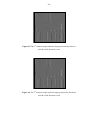
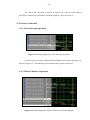
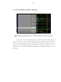
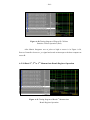
Figure 6.1
st
The 1 moment output statistics image
generated by software with R is 64, direction is
east
Figure 6.2
81
The 1st moment output statistics image
generated by hardware with R is 64, direction is
east
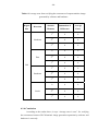
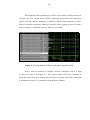
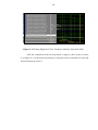
Figure 6.3
81
nd
The 2 moment output statistics image
generated by software with R is 64, direction is
east
Figure 6.4
82
The 2nd moment output statistics image
generated by hardware with R is 64, direction is
east
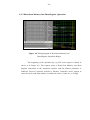
Figure 6.5
82
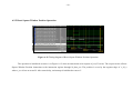
rd
The 3 moment output statistics image
generated by software with R is 64, direction is
east
Figure 6.6
83
The 3rd moment output statistics image
generated by hardware with R is 64, direction is
east
83
Figure A.1
Timing diagram of Memory Read Operation
90
Figure A.2
Timing diagram of Memory Write Operation
91
-x-
Figure A.3
Timing diagram of Memory Clear Operation
(Begin)
Figure A.4
92
Timing diagram of Memory Clear Operation
(End)
92
Figure A.5
Timing diagram of Clear Interrupt Operation
93
Figure A.6
Timing diagram of Write to Memory Operation
(Begin)
Figure A.7
Timing diagram of Write to Memory Operation
(End)
Figure A.8
102
Timing diagram of Calculate GLCM Operation
(End)
Figure A.19
101
Timing diagram of Calculate GLCM Operation
(Finish clearing)
Figure A.18
101
Timing diagram of Calculate GLCM Operation
(Begin)
Figure A.17
100
Timing diagram of Fetch Data into Square
Window Operation (End)
Figure A.16
100
Timing diagram of Fetch Data into Square
Window Operation (Begin)
Figure A.15
99
Timing diagram of Shift Square Window
Position Operation
Figure A.14
98
Timing diagram of Reset Square Window
Position Operation
Figure A.13
97
Timing diagram of Clear Temporary Memory
Operation (End)
Figure A.12
96
Timing diagram of Clear Temporary Memory
Operation (Begin)
Figure A.11
95
Timing diagram of Read from Memory into
Data Register Operation (End)
Figure A.10
94
Timing diagram of Read from Memory into
Data Register Operation (Begin)
Figure A.9
93
102
Timing diagram of Digest GLCM into Statistics
Values Operation (Begin)
103
- xi -
Figure A.20
Timing diagram of Digest GLCM into Statistics
Values Operation (End)
Figure A.21
104
st
Timing diagram of Read 1 Moment into
Result Register Operation
104
Figure A.22
Timing diagram of Initial Image Operation
105
Figure A.23
Timing diagram of Read from Interrupt Register
Operation
106
Figure A.24
Timing diagram of Arbiter Operation
106
Figure A.25
Timing diagram of Center Indexer Operation
107
Figure A.26
Timing diagram of Square Fetcher Operation
(Begin)
Figure A.27
108
Timing diagram of Square Fetcher Operation
(End)
109
Figure A.28
Timing diagram of Square Buffer Operation
110
Figure A.29
Timing diagram of GLCM Builder Operation
111
Figure A.30
Timing diagram of Address Decoder Operation
112
Figure A.31
Timing diagram of Matrix Voter Operation
113
Figure A.32
Timing diagram of Matrix Integrator Operation
(Begin)
Figure A.33
114
Timing diagram of Matrix Integrator Operation
(End)
114
Figure A.34
Timing diagram of Clock Divider Operation
115
Figure B.1
Schematic of Image Processing in Hardware
system
117
- xii -
List of Tables
Pages
Table 2.1
Ports in the local bus of pciif32
Table 2.2
Functions and their descriptions provided in
True PCI DLL
Table 3.1
19
The resulting processing time from varying the
distance
Table 3.2
17
25
result processing time from varying the number
of lines in the buffer
27
Table 4.1
Ports of Memory Controller
35
Table 4.2
Ports of Process Controller
38
Table 4.3
Ports of Arbiter
47
Table 4.4
Ports of Center Indexer
50
Table 4.5
Ports of Square Fetcher
52
Table 4.6
Ports of Square Buffer
56
Table 4.7
Ports of GLCM Builder
58
Table 4.8
Ports of Address Decoder
61
Table 4.9
Ports of Matrix Voter
63
Table 4.10
Ports of Matrix Integrator
65
Table 4.11
Ports of Clock Divider
68
Table 5.1
Design Parameters of Image Processing in
Hardware System
Table 6.1
The result processing time from varying the
number of lines in the buffer
Table 6.2
70
84
Resulting of speed between performed GLCM
image generated by software and hardware for
comparing
85
-1-
Chapter 1
Introduction
Image Processing in Hardware project aims at accelerating image processing
operations by using an FPGA as a co-processor of the computer system. This coprocessor will perform the compute-intensive processing part of those operations.
1.1 Project Background
Digital image processing is one of the most compute-intensive processing in the
world. Obviously, it repeats the same operations on a large amount of data. It is found
that doing the digital image operations by using a computer is slow because the
computer executes very repetitive operations by fetch-execute cycle. The cycle keeps
fetching data and instructions from the storage and executes them one by one not
knowing that it is executing the same operations.
An FPGA does not use the fetch-execute cycle. It can be programmed to
function as a parallel computing unit which takes a large amount of data and does the
same operations to each segment of the data at the same time.
Thus, Image Processing in Hardware project takes the advantages of the FPGA
in speeding the digital image processing. The computationally-intensive operations in a
digital image process will be implemented in the FPGA. For other operations, users
have to implement them in the host computer.
1.2 Project Objectives
1.
Use the FPGA as a co-processor of the computer system in computing
the computationally-intensive part of operations in the digital image
processing.
2.
Study methodology of using the FPGA to build a computing platform
which co-operates in computing with the CPU of the computer.
3.
Make programming of specified algorithms in the FPGA possible for an
applications developer or researcher.
-2-
Chapter 2
Research and Study
In this phase, many image processing operations are studied. Interesting
operations which contains intensively-computational processing are chosen and studied
in detail.
2.1 Related Theories
2.1.1 Digital Image Processing
Digital image processing is used to process digital images to recover
information which is not visible in the original images. It has advantages over analog
image processing – it lets algorithms, which can be implemented only in digital
system, be applied to the input data. Moreover, during the digital process, there is
less noise and distortion than when you using analog processing.
In the past, the cost of digital image processing was very high. This made the
digital image processing limited to a small number of uses. After computers and
dedicated hardware were cheaper, the processing became more popular.
At the present time, computers have more speed than in the past. Computers
now take over the role of most dedicated hardware in the digital image processing
system except processing that related to compute-intensive operations.
2.1.2 Computer Architecture
Present computer architecture is developed from Von Neumann architecture.
Computers in Von Neumann architecture consist of 2 units. They’re a processing unit
and a storage unit. Both data and instructions are stored in the same storage and
processing unit processes them.
The architecture has a bottleneck in processing. When the processor needs to
process a large amount of data, it has to wait for a long time due to throughput of the
transfer between the storage and the processing unit leading to the lack of efficiency
in this architecture.
-3-
In order to process, the processor calls for an instruction in the storage. After
the instruction is fetched to the processor, it executes the instruction. If the
instruction needs input data, the processor will request to fetch the data from the
storage to itself. Then, the execution was successful. This process will be repeated
continuously so it was called “Fetch-execute Cycle”.
Because of the cycle, the architecture performs slower operation on
intensively-computational processes than an FPGA which executes the operation
without the instruction fetch part of the cycle. This speed difference will be most
important with the process that does the same compute-intensive operation on a large
amount of the data such as the digital image processing operation.
2.1.3 Field-Programmable Gate Array (FPGA)
A Field-Programmable Gate Array is a large-scale integrated circuit (LSI)
which is programmable. It is different from other ICs that can’t be reprogrammed
after they’re manufactured.
The FPGA is programmable because it contains a large number of
programmable logic cells that are capable of perform small logic functions. They are
connected to one another using programmable interconnections in the FPGA. By
programming the devices, a more-complex logic function is formed to suit needs.
At the present time, designing the FPGA circuit configuration begins from
gathering requirements, e.g. inputs and outputs of the circuits, timing constraints, or
area constraints. Then, files called “HDLs” are written to describe the behavior of the
system. The HDLs are behaviorally simulated in the computer to make sure that they
can work properly. After the simulations, the circuit diagrams are generated by
circuit synthesis software in the computer. Finally, the diagrams are mapped to the
technology of the FPGA that will be used by place & route software. The result of
the mapping is a configuration of the FPGA called “Netlist”
Once the netlist is loaded into the FPGA board and the switch is turned on,
the configuration will be applied to the FPGA. Then, the FPGA can perform the
behavior described by those HDLs.
-4-
Advantages of using FPGAs in processing
1.
Perform
computationally-intensive
operations
much
faster
than
computers.
2.
Permit changes by application programmers or researchers.
Disadvantages of using FPGAs in processing
1.
Requires digital hardware knowledge to maximize the efficiency of the
designed system.
2.
Trying new algorithms in the FPGA is more inconvenient than in the
computer program according to the hardware limitation and design
process.
3.
A bottleneck in transferring data between the host computer and the
FPGA board is created.
2.1.4 Hardware Description Language (HDL)
Basic digital circuit designing can be done manually. But it can’t be done
manually or takes a lot of time when the circuit becomes larger and more complex.
Because of this, languages have been developed to describe the behavioral model of
the circuit. Hence, it is possible to use a computer to synthesize a circuit which will
have the desired behavior. These languages are called “Hardware Description
Languages”.
Once describing the behavioral of the system with HDLs is completed, the
HDL files will be analyzed and the circuit is synthesized by synthesis software in a
computer. When the circuit is generated, the HDLs complete their responsibility.
Moreover, HDLs are useful in verification of the designed system. They’re
used in behavioral simulations of the system before the circuit is mapped to the
technology to verify correctness of results and basic timing diagrams.
There are 2 HDLs that mostly used. They are Verilog HDL and VHDL. They
are a little different but give the same synthesis result.
Nowadays, high-level languages such as C and Java are developed to
abstractly describe the behavior of the circuit. This makes the design process easier
-5-
than using HDLs but those languages need special compiler programs to generate the
netlist or to convert them to HDLs. The most popular one is ImpulseC. With
ImpulseC, you can use C language to describe circuits and can debug them as C
programs. The compiler facilitates the design process bypassing many tasks – writing
HDLs, synthesizing, etc. Moreover, the compiler makes the description of the circuit
become more abstract because it is not necessary that designers must have knowledge
related to hardware before using it.
With those high-level language compilers, the design process can be finished
faster than using only HDLs and more easily used by C programmers.
2.1.5 Finite State Machine (FSM)
Finite State Machine is a behavioral model which consists of a finite number
of states and transitions between the states. In different states, the action of the model
is also different. It differently obtains inputs and produces outputs in each state.
When sufficient condition occurs, the state will transit to a state that suits the
condition.
States, transitions, and actions can be illustrated in a diagram called “State
Diagram”.
The model is very suitable in designing control devices and processing
devices, such as an elevator controller or a calculator, because they need to perform
different actions in the different input conditions. It is also appropriate in
programming image processing using the FPGA.
2.1.6 Communication Connectivity between an FPGA Board and a
Computer
The connection between the FPGA board and the computer is the bottle-neck
of processing data outside the CPU. Possible connections are …
2.1.6.1 Connect Directly to the PCI Bus of the Computer
Peripheral Component Interconnection (PCI) is a local bus which connects
directly with the processor bus or system bus of the computer.
-6-
Specifications
1.
33.33 MHz clock with synchronous transfers
2.
Data transfer rate is 133 MB per second for 32-bit bus width
3.
3.3 or 5 V signaling
Implementation Possibility
This connection provides the fastest transfer rate over other connections. It
greatly reduces the effect of the bottle-neck to the system.
In spite of the profit from the speed, the FPGA board, which contains an
FPGA, must provide the connector to the PCI slot of the computer and there must
be a PCI controller on the FPGA board. This requires a specialized development
board which is not available at KMUTT.
2.1.6.2 Connect via the 1000BASE-T Gigabit Ethernet
Gigabit Ethernet is a computer network connection according to the IEEE
802.3z standard. 1000BASE-T is a type of this connection which uses category-5
unshielded twisted pair (UTP-5) cables to connect between devices.
Specifications
1.
Serial data transfer
2.
Data transfer rate is up to 128 MB per second (1000 Mb per
second)
3.
Use Carrier Sense Multiple Access / Collision Detection protocol
(CSMA/CD)
4.
Support full-duplex communication
Implementation Possibility
Transferring data through the network requires packaging data into a
packet which wastes data space to the packet header. This reduces the transfer rate
of the real data. Even if the FPGA board can operate in the physical layer of the
TCP/IP model, sending data from the computer to the FPGA board still requires
specials commands and the encapsulation according to the protocol of the model,
e.g. IP header, Data Link header.
-7-
Moreover, if the FPGA board provides only the physical layer of the model
and there is no Gigabit Ethernet Controller in the board, TCP/IP stack must be
implemented separately as a part of the FPGA.
The development board at KMUTT includes a “soft” Ethernet core which
may be 1000 Mb per second or may be only 100 Mb per second. Implementation
in the host computer side is very easy using standard sockets protocol.
2.1.6.3 Connect via Universal Serial Bus
Universal Serial Bus (USB) is a standard connection between electronic
devices including computers. The outstanding features of this connection are
portable and hot-pluggable.
Specifications
1.
Serial data transfer
2.
Support 3 modes of data transferring
-
Low Speed mode with 192 KB per second (1.5 Mb per
second) required 0.0 – 0.3 V
Full Speed mode with 1.5 MB per second (12 Mb per second)
High Speed mode with 60 MB per second (480 Mb per
second) required 2.8 – 3.6 V
3.
Support half-duplex communication
4.
Use differential signaling
Implementation Possibility
Using this connection, the host computer requires USB Host Controller
connected to the PCI bus of it and USB Host Controller Driver to control the data
transfer between devices and the computer.
Device drivers are necessary in communication between a host and
devices. Thus, the FPGA board must have a USB controller to handle the USB
protocol in communication between the board and the host, and the driver for the
board is necessary, as well.
The protocol of this connection uses packets in the communication. Not
only the real data is transmitted but the header of the packets is also transmitted.
The protocol also specified transaction of packets to be sent. For example, if a
-8-
host wants to send data to a device, handshake packets must be sent to each other
to ensure the availability of the communication.
According to the non-data bits sending along with the real data in the
packets, the real transfer rate of this connection is lower than the 60 MB per
second for the High Speed mode. This caused a bottleneck to be created in the
system.
Implementation of a high-speed driver in the host side is reported to be
difficult.
2.1.6.4 Connect to the PCI bus via an I/O Board
By using the PIO-24.PCI I/O board as an intermediate between the FPGA
board and the computer, it allows the FPGA board be connected to the PCI bus for
transferring data between the FPGA and the computer.
Specifications
1.
24-bit bus width to the development board via a 50-pin IDC
connector with half of the pins connected to the ground
2.
5 V signaling
Implementation Possibility
The I/O board uses 8 bits out of 32 bits of the PCI bus as its instruction
port to control its operation. The other 24 bits of the bus is connects to the FPGA
board. The speed of the 24-bit depends on the circuit of the I/O board.
Predictably, if it uses the same clock frequency as the PCI bus, the transfer
rate will be 99.99 MB per second (3 bytes x 33.33 MHz). However, the boards
available at low-cost are much slower-probably only 3 MB per second.
With this connection, FPGA development boards that support 24 or more
I/O pins can be use in this project. Moreover, they must support 5 V signaling. If
they don’t, the driver circuit must be used to convert the lower voltage to 5 V.
2.2 Gray-level Co-occurrence Matrix Statistics Image Generation
This is an image processing operation which is chosen to be a representation of
other image processing operation. The operation generates statistics images from a large
fine image, e.g. a satellite image which contains about 1000 million pixels.
-9-
2.2.1 Description
Gray-level Co-occurrence Matrix statistics images are images which represent
the statistic uniqueness of textures in an image. Many statistics images are generated
from an input image with each different from the others because each different image
is generated from a different gray-level co-occurrence matrix which is unique in
distance and direction.
These statistic images describe a texture so they can be used in texture
detection and texture segmentation by comparing the statistics images generated from
a pattern image to those generated from a segment of the image in which the texture
detection or segmentation is needed.
2.2.2 Theories
2.2.2.1 Gray-level Co-occurrence Matrix (GLCM)
GLCM is a square matrix which contains numbers of times that patterns of
2 scaled values are found while examining pairs of pixels through an image. The
row and column indexes of the GLCM represent the possible scaled values of an
interesting pixel and a pixel which corresponds to the specific direction and
distance from the interesting pixel. Thus, size of the matrix is equal to the number
of all possible scaled values, e.g. 256 values. Each position in the matrix
represents a pattern of a pair of scaled values and the number of times that the
pattern is found in the image is stored in the position.
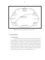
Figure 2.1 Directions from an interesting pixel in an image
- 10 -
An example of a GLCM with 8-scale levels and 1-pixel distance in east
direction is shown below to describe how a GLCM is generated.
Figure 2.2 GLCM with 8-scale levels and 1-pixel distance in east direction
[Source: http://matlab.izmiran.ru/help/toolbox/images/enhanc15.html]
From Figure 2.2, position (1, 1) in this GLCM contains the value 1
because, in the scaled image, there is only one time that a pattern of an interesting
pixel value and its corresponded-pixel value is (1, 1).
Position (1, 2) in this GLCM contains the value 2 because, in the scaled
image, the pattern of an interesting pixel value and its corresponded-pixel value
which is (1, 2) is found twice.
The other values in the GLCM can be derived in the similar way.
2.2.2.2 Calculating Statistics Value for a GLCM
The statistic value is a representation of every value in a matrix. For a
GLCM, the k-th moment method is used in representing. It can be calculated as
follow …
Statistick = ∑∑ ( i − j ) × GLCM i , j
k
j
i
Where k is a natural number
Only the 1st, 2nd and 3rd moments are calculated for the GLCM Statistics
image generation.
- 11 -
2.2.3 Processes
GLCM statistics image generation processes are as follows …
1.
Open an input image.
2.
Set distance value used in GLCM calculation process to 1.
3.
Process the image using a moving window of pixel lines. The number of
lines is specified by user but is limited by the available memory.
4.
For each location of the window, a square area with its size specified by
users is set up with its center at each pixel in the window.
5.
Then, the northeast, east, southeast and south direction GLCMs are
created calculating on pixels within each square area.
6.
For each GLCM created in a square area, the 1st, 2nd and 3rd moments are
calculated.
7.
Three statistics values for each GLCM are stored in separated imageequal-sized buffers at the same position of the center of each square area.
Here twelve image-equal-sized buffers are needed because the GLCMs
are created for four directions and there are three statistics values for
each direction.
8.
Once all twelve buffers are fully filled. twelve statistics images are
generated.
9.
If the distance is not more than half of the size of the square area, the
processes, which are Steps 3 to 8, are repeated with the distance value
increased.
10.
Finish the generation.
- 12 -
Figure 2.3 Flow chart of the GLCM statistic image generation
- 13 -
2.2.4 Reasons for Choosing GLCM
This operation is chosen to be implemented in hardware because it performs
many iterative and intensively-computational processes. Those processes are
performed for each square area of pixels in the input image. four GLCM types for
northeast, east, southeast and south direction are calculated for each square area. For
each direction, GLCMs are calculated for all distance values. The 1st, 2nd and 3rd
statistic moments are calculated for each GLCM and stored in the output buffer at the
same position of the center of the square area. The next interesting square area is
chosen by moving its center to the next pixel. These processes continue until all
statistic values store in the output buffer. Once the buffer is fully filled a statistics
image is created.
A statistics image is generated for each k-th moment statistic calculation of
each different type of the GLCM. Thus, there are 3 moments × 4 directions × ½ of
the square size images needed to be created.
In software, these processes are performed by the fetch-execute cycle of the
computer system. The processes must be performed in order. This can be optimized
using hardware which is capable of perform processes that are not depend on the
others concurrently, and also which does not require the extra time for the instruction
fetch part of the fetch-execute cycle.
2.2.5 Problem Issues
When generating four GLCMs the main step is to examine all pixels and their
corresponded pixels to fill the GLCM. Thus, there are two possible ways in
implementing this algorithm as follow …
1.
Compute each matrix one after another.
2.
Compute all four matrices in one loop.
Filling all four GLCMs concurrently within one round of examining pixel by
pixel in the image shortens the steps in calculating GLCMs for a square area but it
consumes memory and may suffer from the lack of locality of references which is
required by the fetch-execute cycle of the computer system.
- 14 -
As each algorithm above has some difference in its trade-offs, both algorithms will
be tested for determining the fastest algorithm to be implemented in the GLCM
statistic image generation operation in the experimental phase.
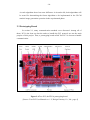
2.3 Prototyping Board
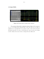
In section 2.1, many communication methods were discussed. Among all of
them, PCI is the best one but the tasks to handle the PCI protocol are not the main
purpose of this project. Thus, a prototyping board called True PCI is chosen to handle
communication.
Figure 2.4 True PCI, the FPGA prototyping board
[Source: True PCI User Manual rev. 1.2, Design Gateway Co., Ltd., page 4]
- 15 -
2.3.1 Description
True PCI is an FPGA prototyping board developed by Design Gateway Co.,
Ltd. It has built-in PCI interface which can be fit in any type of 32-bit PCI slot.
Moreover, the manufacturer provides the 32-bit PCI interface intellectual property
core (IP Core), the windows driver, the dynamic link library and the example
application. These resources are essential for an FPGA designer who is not used to
the PCI protocol so that the designer shouldn’t have to implement them by himself.
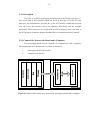
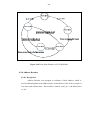
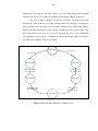
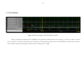
2.3.2 Connectivity between the Board and a Computer
The prototyping board uses PCI interface to communicate with a computer.
The components in are divided into 2 sections as followed…
1.
Prototyping-board-side Section
2.
Computer-side Section
Figure 2.5 Model of the connectivity between the prototyping board and a computer
- 16 -
2.3.2.1 Prototyping-board-side Section
This section contains an IP core, called "pciif32”, which capable of
sending and receiving PCI protocol commands and data to or from a computer via
PCI bus. The core also provides ports interfacing with user-designed IP cores
inside the FPGA via local bus.
Figure 2.6 Local-bus signals of pciif32 interfacing with a user IP core
[Source: True PCI User Manual rev. 1.2, Design Gateway Co., Ltd., page 13]
- 17 -
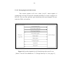
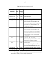
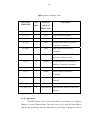
Table 2.1 Ports in the local bus of pciif32
Port Name
Size
Direction
[MSB:LSB]
(bits)
Based on
Description
pciif32
lbaddr[14:2]
13
Input
Address Signal
lbdatain[31:0]
32
Input
Input Data Signal
lbdataout[31:0]
32
Output
Output Data Signal
lbrdb
1
Output
Active-low Read Signal
When this signal goes low, it shows that
there is a read request from the computer and
pciif32 will read data from lbdatain and
sending to the computer.
1
lbwrb
Output
Active-low Write Signal
When this signal goes low, it shows that
there is a write request from the computer
and pciif32 will send out the data through
lbdataout during the time that this signal
remaining low.
1
lbcsb
Output
Active-low Chip Select Signal
When this signal goes low, it shows that the
user IP core is selected to be active.
1
lbint
Input
Interrupt Signal
Interrupt Signal coming from user IP core to
be sent as an internal interrupt to the CPU.
vendorid[15:0]
16
Input
User-defined Vendor ID (Default: 0xF0F0)
deviceid[15:0]
16
Input
User-defined Device ID (Default: 0xF0F0)
The designer of pciif32 also defined a communication protocol between
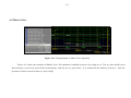
the user IP core and the pciif32 by timing diagrams below…
- 18 -
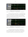
Figure 2.7 Read operation timing diagram
[Source: True PCI User Manual rev. 1.2, Design Gateway Co., Ltd., page 14]
Read operation signals are shown in Figure 2.7. The operation writes data
0x00007777 to the address 0x0003. The Figure shows that after the address signal
is changed for 30 ns, the chip select and read signals will go low and the data
should be sent to lbdatain bus during 60 ns after those signals goes low. The data
will be read by pciif32 and sent to the PCI bus master.
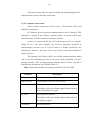
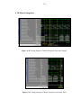
Figure 2.8 Write operation timing diagram
[Source: True PCI User Manual rev. 1.2, Design Gateway Co., Ltd., page 15]
Write operation signals are shown in Figure 2.8. The figure shows
protocol of writing data 0x00007777 to address 0x0003. After the address and
data-out signals are changed for 30 ns, the chip select and write signals will go
low and the user-design core must read the data from the bus within 60 ns.
- 19 -
This section reduces the user task in learning and implementing the PCI
communication protocol in his/her own design.
2.3.2.2 Computer-side Section
There are three components in this section – PCI Interface, Driver and
Dynamic Link Library.
PCI Interface provides physical communication in the PCI protocol. This
component is already in the ordinary computer system. It consists of PCI port,
internal PCI bus, PCI Bus Controller, Memory Controller.
A driver is required by the True PCI card because pciif32 is a customdesign IP core. The driver handles the low-level functional operation in
communicating with the core. A True PCI driver is already provided by the
manufacturer; however, the driver can be used only in Microsoft Windows™
(Win32) system.
The Dynamic Link Library (DLL) is a file that contains functions which
will be used in controlling the driver to do some certain operations. True PCI
package includes a DLL working properly with the True PCI driver. The list of
functions and descriptions is provided in Table 2.2.
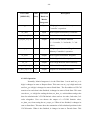
Table 2.2 Functions and their descriptions provided in True PCI DLL
Function
Description
InitDevice
Initialize the device and retrieve the device handler.
ChkDeviceCnt
Count number of devices in the system.
reg_read
Read data from an address
The address will set the lbaddr signal and the data will
be read from lbdatain signal.
reg_write
Write data to an address
The address will set the lbaddr signal and the data will
set lbdataout signal.
CloseDevice
Finalize the device.
- 20 -
2.4 Static Random Access Memory (SRAM)
According to the FPGA specification, there are some distributed RAMs inside
the FPGA on the prototyping board but image processing operations consume a lot of
memory so that those RAMs is not enough. The solution is an external SRAM.
2.4.1 Description
SRAM is an electronic memory which is capable of storing data as long as
there is the power supply for the device. The word ‘Random Access’ means that the
time used in accessing every data in it is always constant.
2.4.2 Operation
The SRAM was chosen to be used in this project is AMIC LP621024D.
Its access time is 75 ns. It was chosen because it has 128k × 8 bit size of memory
and it can be fit in the prototyping board. Because of the high access time despite
high-speed clock signal (33 MHz), the speed of the processing is slowed down
because of this bottle neck.
The operation of this SRAM is controlled by four signals – Active-low
Chip Enable 1 (ce1_n), Chip Enable 2 (ce2), Active-low Write Enable (we_n), and
Active-low Output Enable (oe_n). Additional signals are a 17-bit Address Signal
(Address[16:0]) and a 8-bit Data Signal (Din[7:0], Dout[7:0])
Read operation can be performed by continuously setting both ce1_n and
oe_n to low voltage, and both we2_n and ce2 to high voltage. Then, changing
Address to the required address will read the data from the SRAM and send it out
to data after 75 ns. This operation is shown in Figure 2.9.
- 21 -
Figure 2.9 Timing Diagram of the SRAM Read Operation
[Source: AMIC LP621024D Data Sheet, AMIC Technology, Corp., page 6]
Write operation is shown in Figure 2.10. The oe_n is constantly at low
voltage. Begin with changing Address signal to the address which needs to be
written and set ce1_n to low voltage and both ce2 and we_n to high voltage, then
after 15 ns, toggle we_n to another state. The write operation will be performed
during the overlapped time of high ce2, low ce1_n and low we_n, thus the data to
be written must be present during this period. After about 60 ns, those signals will
be toggle again and the operation is finished.
Figure 2.10 Timing Diagram of the SRAM Write Operation
[Source: AMIC LP621024D Data Sheet, AMIC Technology, Corp., page 6]
- 22 -
Note that, the SRAM is a 5V device but the FPGA prototyping board is a
3.3V one. Thus, a bi-directional level-shifter circuit is needed in the system. 150Ω
resisters are used to solve this problem because getting a 3.3-to-5 volt converter
circuit is very difficult in Thailand. The circuit is shown in Figure 2.11.
Figure 2.11 The bi-directional level-shifter circuit
- 23 -
Chapter 3
Experiments
Experiments in this phase are set up to obtain the fastest algorithm for each
operation when performed by PC software. The processing time of each operation is
recorded to be compared with the processing time performed by hardware. Moreover,
the outputs of each operation are obtained to be used in verifying correctness of the
outputs obtained from the operation performed by hardware.
3.1 Possible Algorithms for Gray-level Co-occurrence Matrix
3.1.1 Introduction
The GLCM can be implemented in the code in 2 ways. They are …
1.
Compute each matrix one after another. (m01)
2.
Compute all four matrices in one loop. (m02)
Each of them has different advantages and disadvantages as mentioned in the
previous chapter. The main object of this experiment is to find the best algorithm to
be implemented in the GLCM statistics image generation operation.
- 24 -
3.1.2 Objectives
1.
To obtain the fastest algorithm for calculating GLCMs in four directions
(i.e. northeast, east, southeast and south)
2.
To examine effects of varying arguments of GLCM operation on
processing time
3.
To examine processing characteristics of a computer system
3.1.3 Materials and Equipments
1.
Executable files of each algorithm which implements timer functions in it
2.
An Open Dragon image which its size is 3822 pixels by 2560 pixels
3.
A Computer with these specifications
a. CPU:
Intel Pentium 4 1.6 GHz
b. Motherboard: IBM, Intel i845
c. RAM:
DDR 640 MB, 133 MHz
3.1.4 Procedures
1.
Execute m01 algorithm with the image, and 16-pixel distance. Observe
and record the processing time and GLCMs generated.
2.
Repeat step 1 but using the m02 algorithm instead of the m01 algorithm.
3.
Repeat step 1 - 2 but change the distance into 1, 128, 512 and 1024
respectively.
- 25 -
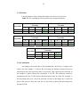
3.1.5 Results
Vary the distance (D) by fixing the number of scale levels to 8 levels.
Table 3.1 The resulting processing time from varying the distance
Algorithm
m01
m02
Algorithm
m01
m02
Processing Time with D = 1
(seconds)
1
2
3
Mean
5.813
5.829
5.844
5.829
5.813
5.829
5.844
5.829
Processing Time with D = 16
(seconds)
1
2
3
Mean
5.781
5.797
5.797
5.792
5.828
5.860
5.859
5.849
Processing Time with D = 128
(seconds)
1
2
3
Mean
5.750
5.750
5.735
5.745
5.782
5.782
5.797
5.787
Processing Time with D = 512
(seconds)
1
2
3
Mean
5.532
5.532
5.531
5.532
5.547
5.563
5.547
5.552
Algorithm
m01
m02
Processing Time with D = 1024
(seconds)
1
2
3
Mean
5.250
5.250
5.250
5.250
5.266
5.266
5.266
5.266
3.1.6 Conclusion
According to the results above, the algorithm m01 which says “Compute each
matrix one after another.” is fastest. By increasing the distance measured between
interesting pixels, the processing time is decreased. This caused by the reduction in
the number of pixels taking into calculation a GLCM. The reduction cannot be
avoided because the GLCM requires that both pixels must be valid. For example, if
the interesting pixel was 5-pixel far from the east side of the image, the 10-pixel-far
pixel to the east of it does not exist. So it is necessary to ignore the interesting pixel
for that GLCM.
- 26 -
Because the algorithm m01 is faster than m02 it is illustrated that the
computer fetch-execute cycle will work well if the processing data has some locality
of references, e.g. the next data is nearby the processing data. To emphasize the idea,
in the m01 algorithm, a GLCM is processed one by one which means that a pair of
interesting pixels is always in the same direction and distance. Unlikely, in m02, all
four GLCMs is filled at the same time. This causes the CPU of the computer to fetch
the next interesting pixel which is not in the same direction of the processing pixel.
3.2 Gray-level Co-occurrence Matrix Statistics Image Generation
3.2.1 Introduction
This operation generates many statistics images from many GLCMs of
specified-size square segments of the input image. Two arguments are required for
generating the statistic images from an input image. They are …
1.
The size of square areas of pixels of the input image using in calculating
GLCMs for each direction (i.e. northeast, east, southeast and south)
2.
The number of rows of pixels that can be in a buffer which is used to
divide images into regions
3.2.2 Objectives
1.
To obtain the processing time of this operation performed by software for
being compared to the processing time performed by hardware in the
later phase
2.
To obtain the output statistics image used in verifying the correctness of
the operation performed by hardware in the later phase
- 27 -
3.2.3 Materials and Equipments
1.
Executable file of the GLCM Statistics Image Generation Operation
which implements timer functions in it
2.
Two tagged Image File Format images (TIFF image) whose sizes are 16
pixels by 16 pixels and 272 pixels by 280 pixels
3.
A Computer with these specifications
a) CPU:
Intel Celeron 2.4 GHz
b) Motherboard: IBM, Intel i845
c) RAM:
DDR 512 MB, 133 MHz
3.2.4 Procedures
1.
Execute the operation with the 16-by-16-pixel TIFF image, 3-by-3-pixel
square size and 16-line region buffer. Observe and record the processing
time and output statistics image generated.
2.
Repeat step 1 but change the image to 272-by-280-pixel TIFF image and
the number of lines in the buffer to 240.
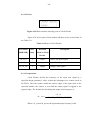
3.2.5 Results
Vary the number of lines in the buffer (R) by fixing the number of scale
levels to 256 levels and size of square areas of pixels to 3.
Table 3.2 The result processing time from varying the number of lines in the buffer
Processing Time
Image Size
Region Size
(pixels)
(lines)
16x16
16
38.13
38
272x280
240
14682.24
14682
(seconds)
CPU Time Wall Time
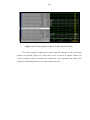
- 28 -
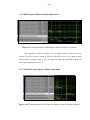
3.2.6 Conclusion
The result processing time and images is obtained. The processing time shows
that when increasing the number of pixels, the processing time increases linearly.
The output statistics images show that sections of the image which have the
same pattern will be shown in the result images by the same gray level. The 2nd
moment statistics images are different from the 1st and 3rd moment. They bring
contrast of the patterns in the input image into sight.
- 29 -
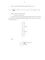
Chapter 4
Designs
After research & study and experiment have been done, the system was designed
to resolve problems facing in software. The first goal of designing the system is to speed
up the processing time of image processing operations and the GLCM statistic image
generation was selected as an example. The second is to generalize image processing
operations into building blocks which functions independently so that the system can be
easily expanded or modified later.
All designs in this chapter are based on hardware devices listed below…
1.
Prototyping Board: Design Gateway True PCI
2.
SRAM: AMIC LP621024D
3.
Bi-directional Buffer: 150Ω Resistors
4.1 Top-level Design of the System
As discussed above, the system is divided into functional blocks. Thus, the
system is composed of blocks and buses. There are two buses in the system – the 17-bit
Address bus and the 8-bit Data bus. Length of each bus is defined by the external
SRAM used.
- 30 -
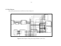
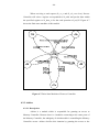
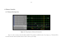
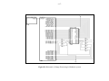
4.1.1 Block Diagram
Names and connections between each block are shown in Figure 4.1.
Figure 4.1 Block diagram of Image Processing in Hardware system (Top)
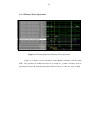
- 31 -
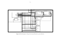
Figure 4.2 Block diagram of Image Processing in Hardware system (Bottom)
- 32 -
4.1.2 System Components
There are 13 modules in the system. They are …
1.
Memory Unit
2.
Process Controller
3.
Memory Controller
4.
Arbiter
5.
Center Indexer
6.
Square Fetcher
7.
Square Buffer
8.
GLCM Builder
9.
Address Decoder
10.
Matrix Voter
11.
Matrix Integrator
12.
Clock Divider
13.
pciif32
4.1.3 Top-level System Operation
All components work together by exchanging digital signals between one
another. The system operation starts from the host computer. By calling the
‘initDevice’ function, pciif32 will take care of initializing the device.
Once the device has been initialized, instructions will be sent to the device by
calling ‘reg_write’ function with proper arguments – a 32-bit instruction/data to be
sent and an address to send instruction/data to. pciif32 will perform a write operation
through the local bus with the specified instruction/data to the specified address.
Then, proc_ctrl will receive the instruction and control the others modules to
operate the received instruction. If the instruction is to read data, proc_ctrl will
prepare the data to be ready for the next call to ‘reg_read’ function.
When a ‘reg_read’ function is called, pciif32 will perform a read operation
from the local bus with the specified address. According to the read operation,
- 33 -
proc_ctrl will be responsible for presenting the data during the low-voltage duration
of cs_n and rd_n.
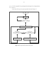
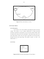
A flow chart of the top-level system operation is shown in Figure 4.3.
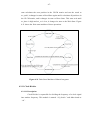
Start
Idle
No
Is initDevice called?
Yes
Wait for a read or write operation
No
Is a write operation
performed?
No
Is a read operation
performed?
Yes
Yes
Do the instructed operattion
Send the requested data to the local bus
Figure 4.3 The top-level flow chart of the system
- 34 -
4.2 Component Designs
The system is divided into modules for generalization. This section provides
information of how each module is designed and what is its operation.
4.2.1 Memory Controller
4.2.1.1 Description
Memory Controller takes care of reading from and writing to the SRAM.
A read or write request comes from other modules which need to access data
within the SRAM. Once the request is received, the memory controller signals the
SRAM as in Figure 2.9 or Figure 2.10 for a read or write request, respectively and
notifies the requester about the completion. This module is named “mem_ctrl” and
abbreviated as “mc”.
4.2.1.2 Ports
Figure 4.4 Block structure showing ports of Memory Controller
Figure 4.4 shows ports of this module and those ports are described in the
Table 4.1
- 35 -
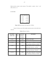
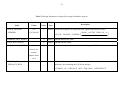
Table 4.1 Ports of Memory Controller
Port Name
Size
Direction
[MSB:LSB]
(bits)
Based on
Description
Memory
Controller
mc_clk
1
Input
Clock Signal from Clock Divider
mc_rst_n
1
Input
Active-low Reset Signal
mc_en
1
Input
Enable Signal
mc_rw
1
Input
If low, activate the read operation.
If high, activate the write operation.
mc_clr_n
1
Input
If low, clear temporary memory.
mc_addr[16:0]
17
Input
Address used in the read/write operation
mc_done
1
Output
Done Signal to notice other modules
sr_ce1_n
1
Output
Active-low Chip Enable 1 of SRAM
sr_we_n
1
Output
Active-low Write Enable of SRAM
sr_oe_n
1
Output
Active-low Output Enable of SRAM
sr_ce2
1
Output
Chip Enable 2 of SRAM
bf_dir
1
Output
Bi-directional Level Shifter Direction
dbg_mc_st[3:0]
4
Output
Memory Controller State LEDs (debug)
mc_data[7:0]
8
Bi-direction Data to be written or read in the operation
sr_data[7:0]
8
Bi-direction Data Signal of SRAM
4.2.1.3 Operation
Normally, Memory Controller is in the Wait State and controls all SRAM
signals to operate in the reading operation until mc_en is changed to high or
mc_clr_n is change to low.
If mc_en is high, it checks mc_rw whether it is low or high. If mc_rw is
high, it will change its state to Read State, change sr_addr to be the same as
mc_addr (received address) to read the data, put the data to mc_data, and return to
- 36 -
the Wait State. If mc_rw is low, it will change its state to Write State, perform a
write signaling, and return to the Wait State.
Otherwise, if mc_clr_n is low when Memory Controller is in the Wait
State, it will change its state to Clear State. When it is in Clear State, a clear flag is
set, a counter is started, and the state changes into Write State. During SRAM
write operation, if the flag is set Memory Controller will write a zero number to
the address which equals to starting address of the temporary memory plus a
number in the counter, and return to the Clear State for adding the counter. If the
counter reaches the size of the temporary memory, the clear process will be done
and the controller will return to the Wait State. Otherwise, it continuously goes to
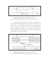
the Write State. Figure 4.5 shows the finite state machine of these operations.
Wait
State
Read operation
is done.
mc_clr_n is low.
Counter reaches
size of temporary memory.
mc_en is high.
mc_rw is high.
Read
State
Write operation
is done.
Clear Flag is clear.
mc_en is high.
mc_rw is low.
Clear
State
Write operation
is done.
Clear Flag is set.
Counter doesn’t reach size of
temporary memory.
Write
State
Figure 4.5 Finite State Machine of Memory Controller
- 37 -
4.2.2 Process Controller
4.2.2.1 Description
Process Controller was designed to control the other modules and
provide relevant information for their processing. It is controlled by pciif32 and
operates as instructed by combinations of local bus address and data signals.
Moreover, this module also manages interfacing with pciif32, interrupt generating
and error reporting. This module is named “proc_ctrl” and abbreviated as “pc”.
4.2.2.2 Ports
Figure 4.6 Block structure showing ports of Process Controller
Figure 4.6 shows ports of this module and those ports are described in the
Table 4.2.
- 38 -
Table 4.2 Ports of Process Controller
Port Name
Size
Direction
[MSB:LSB]
(bits)
Based on
Description
Process
Controller
pc_clk
1
Input
33MHz Clock Signal
pc_rst_n
1
Input
Active-low Reset Signal
pc_gnt
1
Input
If high, gain control of Memory
Controller’s operation.
sf_done
1
Input
Done Signal from Square Fetcher
gb_done
1
Input
Done Signal from GLCM Builder
mi_done
1
Input
Done Signal from Matrix Integrator
mc_done
1
Input
Done Signal from Memory Controller
lb_cs_n
1
Input
Chip Select Signal from pciif32
lb_wr_n
1
Input
If low, pciif32 is performing a write
operation.
lb_rd_n
1
Input
If low, pciif32 is performing a read
operation.
lb_addr[12:0]
13
Input
Address of the register participated in
the operation of pciif32
lb_data_out[31:0]
32
Input
Data to be read/write to the register
addressed by lb_addr
pc_req
1
Output
If high, Process Controller request for
controlling Memory Controller’s
operation from Arbiter.
ci_ld_n
1
Output
If low, reset Center Index’s row and
column indices to zeroes.
ci_nxt
1
Output
If high, shift indices of Center Index to
the next pixel co-ordinate.
- 39 -
Port Name
Size
Direction
[MSB:LSB]
(bits)
Based on
Description
Process
Controller
sf_en
1
Output
Enable Signal for Square Fetcher
gb_en
1
Output
Enable Signal for GLCM Builder
mi_en
1
Output
Enable Signal for Matrix Integrator
mc_en
1
Output
Enable Signal for Memory Controller
mc_rw
1
Output
Read/Write Control Signal for Memory
Controller
mc_clr_n
1
Output
Active-low Temporary Memory Clear
Enable Signal for Memory Controller
lb_int
1
Output
If high, send an interrupt to the host
computer.
mi_output_sel[1:0]
2
Output
Select which results of Matrix
Integrator should be present at
mi_data_out
img_width[9:0]
10
Output
Width of the target image
img_height[9:0]
10
Output
Height of the target image
gb_dx[3:0]
4
Output
Different in horizontal direction of the
interesting pixel in building the GLCM
gb_dy[3:0]
4
Output
Different in vertical direction of the
interesting pixel in building the GLCM
dbg_pc_st[3:0]
4
Output
Process Controller State LEDs (debug)
vendor_id[15:0]
16
Output
Vendor ID Number (Default: 0xF0F0)
device_id[15:0]
16
Output
Device ID Number (Default: 0xF0F0)
img_addr[16:0]
17
Output
Starting Address of the target image
mc_addr[16:0]
17
Output
Address used in operation of Memory
Controller
- 40 -
Port Name
Size
Direction
[MSB:LSB]
(bits)
Based on
Description
Process
Controller
32
lb_data_in[31:0]
Output
Data to be sent to the host computer
when a read request from pciif32
occurred.
8
mc_data[7:0]
Bi-directional
Data read from or to be written to
Memory Unit by Memory Controller
4.2.2.3 Operations
Process Controller controls operations of the other components except
Arbiter. It receives instructions from the host computer through lb_addr and
lb_data_out of the pciif32 write operation.
32-bit instructions were designed to controls operations of the system.
Note that, addresses below must be right-shifted by 2 to be correctly used in the
‘reg_read’ or ‘reg_write’ functions because the range of MSB to LSB of lbAddr
of pciif32 is [14:2] but lb_addr of Process Controller is [12:0], respectively. They
are…
1.
Clear Interrupt
Description:
Clear the interrupt produced by Process Controller.
lb_addr:
0x0000
lb_data_out: All bits are 0’s.
2.
Write to Memory
Description:
Write an 8-bit data to the specified address in the external
memory.
lb_addr:
0x0001
lb_data_out: bit 24 – 8
bit 7 – 0
Other bits are 0’s.
A 17-bit address to be written
An 8-bit data to be written
- 41 -
3.
Read from Memory into Data Register
Description:
Read an 8-bit data from the specified address in the
external memory.
lb_addr:
0x0001
lb_data_out: bit 24 – 8
A 17-bit address to be read
Other bits are 0’s.
4.
Clear Temporary Memory
Description:
Clear temporary memory in the external memory used
during image processing.
lb_addr:
0x0001
lb_data_out: bit 28 is 1.
Other bits are 0’s.
5.
Reset Square Window Position
Description:
Reset position of the square processing window to
position (0, 0) of the input image.
lb_addr:
0x0001
lb_data_out: bit 29 is 1
Other bits are 0’s.
6.
Shift Square Window Position
Description:
Shift the square processing window to the next position in
the input image.
lb_addr:
0x0001
lb_data_out: bit 28 and 29 are 1’s.
Other bits are 0’s.
7.
Fetch Data into Square Window
Description:
Fetch all pixels into the square processing window.
lb_addr:
0x0001
lb_data_out: bit 30 is 1.
Other bits are 0’s.
- 42 -
8.
Calculate GLCM
Description:
Calculate GLCM in the specified direction (dx, dy). dx is
the horizontal different between an interesting pixel and a
target pixel, and dy is the vertical different between an
interesting pixel and a target pixel.
lb_addr:
0x0001
lb_data_out: bit 28 and 29 are 1’s.
bit 15 – 8
dx
bit 7 – 0
dy
Other bits are 0’s.
9.
Digest GLCM into Statistic Values
Description:
Digest a GLCM into 3 statistic values – 1st, 2nd and 3rd
moment statistic values.
lb_addr:
0x0001
lb_data_out: bit 31 is 1.
Other bits are 0’s.
10.
Read 1st Moment into Result Register
Description:
Read the 1st moment statistic value into Result Register.
lb_addr:
0x0001
lb_data_out: bit 27 and 31 are 1’s.
Other bits are 0’s.
11.
Read 2nd Moment into Result Register
Description:
Read the 2nd moment statistic value into Result Register.
lb_addr:
0x0001
lb_data_out: bit 28 and 31 are 1’s.
Other bits are 0’s.
12.
Read 3rd Moment into Result Register
Description:
Read the 3rd moment statistic value into Result Register.
lb_addr:
0x0001
lb_data_out: bit 27, 28 and 31 are 1’s.
Other bits are 0’s.
- 43 -
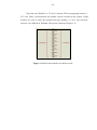
13.
Initialize Image
Description:
Specify width and height of an input image.
lb_addr:
0x0002
lb_data_out: bit 31 – 16
bit 15 – 0
Width of the image
Height of the image
There are 5 32-bit registers related in operations of Process Controller.
Each can be addressed by changing lb_addr to a defined address.
1.
Interrupt Register (Address: 0x0000)
This register controls sending an interrupt to the host computer. If
its bit 0 is set, an interrupt will occur and lb_int will go high. Once set, it
can be cleared by ‘Clear Interrupt’ instruction.
2.
Instruction/Data Register (Address: 0x0001)
This register operates in 2 modes – Input and Output. It operates
in the input mode when there’s a write request with lb_addr is 0x0001
and the register will operate as Instruction Register storing an instruction
which is going to be performed by the Process Controller.
Oppositely, it operates in the output mode when there’s a read
request with the same lb_addr and the register will operate as Data
Register storing the data which is fetched from the specified address in
the external memory with ‘Read from Memory into Data Register’
instruction.
3.
Image Register (Address: 0x0003)
This register holds information of the input images. The
information about the input image’s width and height is declared to the
other modules. This register can be set with ‘Initialize Image’ instruction.
4.
Result Register (Address: 0x0004)
This register contains the result digested value after a ‘Read 1st,
2nd or 3rd Moment into Result Register’ instruction.
- 44 -
5.
Message Register (Address: 0x0005)
This register will be set after each completion of every instruction
to provide error report information to the host computer. Its value can
be…
MSG_OK
The operation is done properly.
MSG_IMAGE_NOT_INIT
Cannot perform requested instruction because ‘Image
Initialize’ instruction has never been received.
MSG_IMAGE_SIZE_INVALID
The specified input image size is larger than the unused
external memory size of the system.
Normally, Process Controller is in the Wait State. Instructions are
received by monitoring when lb_cs_n, lb_wr_n and lb_rd_n signals will go low.
According to pciif32 operations, Process Controller responds to 2 types of
requests from pciif32 – a read request or a write request.
When receiving a write request (lb_cs_n and lb_wr_n are low), if a flag
named ‘is_image_described’ is clear, an ‘Initialize Image’ instruction should be
sent to Process Controller, is_image_described will be set, an interrupt will be
received at the host computer with MSG_OK in the Message Register.
Otherwise, an interrupt occurs and the Message Register is set to
MSG_IMAGE_NOT_INIT. In case of MSG_IMAGE_SIZE_INVALID, an
interrupt occurs but the flag is not set.
If the flag is set, any of the instruction can be received, Process
Controller will move to the Decide State to perform different tasks for each
different instruction except for ‘Clear Interrupt’ and ‘Initialize Image’
instructions.
For ‘Clear Interrupt’ instruction, the instruction register is clear and the
current interrupt is disappeared suddenly without state changing of Process
Controller.
- 45 -
For ‘Initialize Image’ instruction, the Image Register is set, once the
instruction is received without state changing if and only if the size is valid.
Otherwise, an error will be reported.
For the other instructions, Process Controller performs operations as
described below…
For ‘Write to Memory’, ‘Read from Memory into Data Register, or
‘Clear Temporary Memory’ instruction, Process Controller will move into the
mc State. It begins the state by first send a request for controlling Memory
Controller to Arbiter by set pc_req to high. After receive a grant, i.e. pc_gnt is
high, it performs one of 3 Memory Controller’s operations in order to which one
of 3 instructions was received. Once it receives a Done Signal from Memory
Controller, i.e. mc_done is high; it returns mc_en and mc_clr_n to the default
values cancelling the operation and goes back to the Wait State with a MSG_OK
interrupt.
For ‘Reset Square Window Position’ or ‘Shift Square Window Position’
instruction, Process Controller move into the ci State send ci_ld_n negative
square pulse or ci_nxt positive pulse, respectively. Then, it will return to the
Wait State.
For ‘Fetch Data into Square Window’, ‘Calculate GLCM’, or ‘Digest
GLCM into Statistic Values’ instruction, it will move into a corresponding state,
i.e. sf State, gb State, and mi State, to enabling Square Fetcher through a high
sf_en, GLCM Builder through a high gb_en and Matrix Integrator through a high
mi_en, respectively. Once the enabled module is complete its operation and the
Done Signal is received, i.e. sf_done, gb_done, mi_done, Process Controller will
disable the module and return to the Wait State with a MSG_OK interrupt.
For ‘Read 1st, 2nd, or 3rd Moment into Result Register’ instruction,
Process Controller will change into mi State and change mi_output_sel to be the
same as bit 28 down to 27 of the instruction register to order Matrix Integrator to
send the selected data through mi_data_out. After setting the signal, Process
Controller returns itself to the Wait State and sends a MSG_OK interrupt to the
host computer.
- 46 -
When receiving a read request (lb_cs_n and lb_rd_n are low), Process
Controller will select a register corresponded to lb_addr and put the data within
the specified register to lb_data_in for the read operation of pciif32. Figure 4.7
shows the finite state machine of this module.
Figure 4.7 Finite State Machine of Process Controller
4.2.3 Arbiter
4.2.3.1 Description
Arbiter is a module which is responsible for granting an access to
Memory Controller. Because there’re 4 modules connecting to the same ports of
the Memory Controller, the ambiguity of which module is controlling the Memory
Controller occurs. Arbiter clarifies this situation by granting the access to the
- 47 -
highest priority request at that moment. This module is named “arbiter” and
abbreviated as “ar”.
4.2.3.2 Ports
Figure 4.8 Block structure showing ports of Arbiter
Figure 4.8 shows ports of this module and those ports are described in the
Table 4.3.
Table 4.3 Ports of Arbiter
Port Name
Size
Direction
[MSB:LSB]
(bits)
Based on
Description
Arbiter
ar_clk
1
Input
33MHz Clock Signal
ar_rst_n
1
Input
Active-low Reset Signal
pc_req
1
Input
If high, Process Controller is requesting
for controlling of Memory Controller.
sf_req
1
Input
If high, Square Fetcher is requesting for
controlling of Memory Controller.
mv_req
1
Input
If high, Matrix Voter is requesting for
controlling of Memory Controller.
mi_req
1
Input
If high, Matrix Integrator is requesting
for controlling of Memory Controller.
- 48 -
Port Name
Size
Direction
[MSB:LSB]
(bits)
Based on
Description
Arbiter
1
pc_gnt
Output
If high, Process Controller gains control
of the Memory Controller.
1
sf_gnt
Output
If high, Square Fetcher gains control of
the Memory Controller.
1
mv_gnt
Output
If high, Matrix Voter gains control of
the Memory Controller.
1
mi_gnt
Output
If high, Matrix Integrator gains control
of the Memory Controller.
dbg_ar_st[3:0]
4
Output
Arbiter State LEDs (debug)
4.2.3.3 Operations
Arbiter starts from Wait State. When a request signal (which is pc_req,
sf_req, mv_req or mi_req) is set, it will move to Decide State. Within the state,
grant signals (which are pc_gnt, sf_gnt, mv_gnt and mi_gnt) are changed by
granting the request from the highest priority module first, in case of 2 or more
modules request in the same time. The signal connected to the granted module
goes high during granting. The priority of granting can be rearranged from Process
Controller, Square Fetcher, Matrix Voter and Matrix Integrator, descending. After
granting, the state of this module is changed into Grant State. While being in
Grant State, all non-granted-request signals are ignored until the granted-request
signal becomes low. Once the signal goes low, Arbiter will return to the Wait
State and continue its operation. Figure 4.9 shows the finite state machine of this
module.
- 49 -
There is a request.
Wait
State
Decide
State
The granted-request
becomes low.
Grant
State
Figure 4.9 Finite State Machine of Arbiter
4.2.4 Center Indexer
4.2.4.1 Description
Center Indexer is one of the modules representing the square processing
window. This window is one of unique characteristics of image processing
operations. Operations are performed to every pixel in the window and the results
are placed at the center pixel of the result images. Center Index keeps track of row
and column indices of this center pixel and is responsible for moving this index
through all pixels in the input image. This module is named “cen_index” and
abbreviated as “ci”.
4.2.4.2 Ports
Figure 4.10 Block structure showing ports of Center Indexer
- 50 -
Figure 4.10 shows ports of this module and those ports are described in
the Table 4.4.
Table 4.4 Ports of Center Indexer
Port Name
Size
Direction
[MSB:LSB]
(bits)
Based on
Description
Center
Indexer
ci_rst_n
1
Input
Active-low Reset Signal
ci_ld_n
1
Input
If low, calculate and change the index
to the next position.
1
ci_nxt
Input
If high, shift the index to the next
position.
If low, reset the index to (0, 0).
img_width[9:0]
10
Input
Width of the Image
img_height[9:0]
10
Input
Height of the Image
img_addr[16:0]
17
Input
Starting Address of the Image
ci_end
1
Output
If high, indicates that the index reaches
the end of the image.
ci_row[9:0]
10
Output
Row Index of the Window
ci_col[9:0]
10
Output
Column Index of the Window
4.2.4.3 Operations
During the ci_rst_n signal is low, Center Indexer resets itself to the origin
position of the image (0, 0). The index can be shifted to the next position by
setting ci_nxt to high and send a negative-edge signal to ci_ld_n.
If ci_nxt is low when a negative-edge signal has been received at ci_ld_n,
the index will be reset to (0, 0) position.
- 51 -
4.2.5 Square Fetcher
4.2.5.1 Description
Square Fetcher fetches corresponding pixels from the Memory Unit into
the Square Buffer which represents the square processing window. This module
has an advantage over the CPU in the reduction of the time used in fetching pixels
in the window which is virtually nearby one another but physically far away one
another in the memory address space. This module is named “sq_fetch” and
abbreviated as “sf”.
4.2.5.2 Ports
Figure 4.11 Block structure showing ports of Square Fetcher
Figure 4.11 shows ports of this module and those ports are described in
the Table 4.5.
- 52 -
Table 4.5 Ports of Square Fetcher
Port Name
Size
Direction
[MSB:LSB]
(bits)
Based on
Description
Square
Fetcher
sf_clk
1
Input
33MHz Clock Signal
sf_rst_n
1
Input
Active-low Reset Signal
sf_en
1
Input
Enable Signal
sf_gnt
1
Input
If high, Square Fetcher gains control of
Memory Controller.
mc_done
1
Input
Done Signal from Memory Controller
img_width[9:0]
10
Input
Width of the Image
img_height[9:0]
10
Input
Height of the Image
ci_row[9:0]
10
Input
Row Index of the Window
ci_col[9:0]
10
Input
Column Index of the Window
img_addr[16:0]
17
Input
Starting Address of the Image
sf_req
1
Output
If high, Square Fetcher is requesting for
controlling of Memory Controller.
sf_done
1
Output
If high, Square Fetcher is done its
operation.
sb_wr_n
1
Output
Active-low Write Signal
If low, command Square Buffer to store
the data from sb_data_in to the address
specified by sb_wr_addr.
mc_en
1
Output
Enable Signal Memory Controller
- 53 -
Port Name
Size
Direction
[MSB:LSB]
(bits)
Based on
Description
Square
Fetcher
1
mc_rw
Output
Read/Write Control Signal for Memory
Controller
dbg_sf_st[3:0]
4
Output
Square Fetcher State LEDs (debug)
sb_wr_addr[3:0]
4
Output
Address in Square Buffer address space
to fetch data into
mc_addr[16:0]
17
Output
Address used in operation of Memory
Controller
4.2.5.3 Operations
Square Fetcher starts fetching the top-left pixel of the square processing
window. It fetches in left-to-right and top-to-bottom direction. There are 2 finite
state machines in this module – Main FSM and Fetch FSM.
Square Fetcher’s Main FSM originates in Wait State. If sf_en is high, its
state will be changed to Request State. In this state, Square Fetcher sends a
request for controlling the Memory Controller to the Arbiter via a high sf_req
signal. Once sf_gnt is received, the request operation is done and Square Fetcher
moves to Fetch State. Fetch FSM is enabled in this state by setting the “f_en” flag
to logic 1. The Main FSM is now waiting for the logic 1 of “f_done” flag. Once
the flag is set, The Main FSM resets f_en flag and moves to Done State sending
high sf_done to the Process Controller. The done signal is sent continuously until
sf_en is reset to low signal. Once sf_en is reset, the state is looped back to Wait
State wating for sf_en again. Figure 4.12 shows the Main FSM of the Square
Fetcher.
- 54 -
Wait
State
sf_en is high.
sf_en is low.
Done
State
Request
State
sf_gnt is high.
f_done is high.
Fetch
State
Figure 4.12 Main Finite State Machine of Square Fetcher
Fetch FSM originates in its Wait State. Once f_en is high, its state will
changes to Validate State. In this state, the row and column indices of expectedto-be-fetched pixel are validated. If the coordinate is out-of-bound, the row and
column indices will be replaced by the coordinate of the nearest border pixel.
Once the validation process is complete, the FSM will move to Assign State. As
the name of the state, this state assigns a value to the new Square Buffer address
space. It performs a read operation of the Memory Controller with the indexvalidated address. When a high mc_done is received, a negative-edge signal is
generated at sb_wr_n to write the data in the data bus to the address in Square
Buffer address space specified sb_wr_addr. Again, the state changes to Next State
to move the coordinate to the next position and sb_wr_addr is added by 1. If the
coordinate doesn’t reach the end of the square processing window, the FSM
moves to Validate State to continuously perform fetching operations. Otherwise,
if the end of the window is reached, it moves to Done State setting f_done to logic
1 and waiting for a reset of f_en to return to Wait State. This FSM is shown in
Figure 4.13.
- 55 -
f_en is low.
Wait
State
Done
State
f_en is high.
Validate
State
All pixels in the window are
not completely fetched.
All pixels in the window are
fetched.
Address is validated.
Next
State
Assign
State
The pixel in the window is
assigned to Square Buffer.
Figure 4.13 Fetch Finite State Machine of Square Fetcher
4.2.6 Square Buffer
4.2.6.1 Description
Square Buffer represents the square processing window. Its address space
is independent from the Memory Unit address space. Thus, the low-locality-ofreference addressing is changed into one contiguous addressing which speed up
the fetching operation. This module is capable of reading and writing the data to
one of its address at the same time. Moreover, it provides the 2-channelled data
accessing which aids in accessing 2 data at the same time. Hence, accessing 2 data
in the square processing window is another uniqueness of image processing
operation. This module is named “sq_buf” and abbreviated as “sb”.
- 56 -
4.2.6.2 Ports
Figure 4.14 Block structure showing ports of Square Buffer
Figure 4.14 shows ports of this module and those ports are described in
the Table 4.6.
Table 4.6 Ports of Square Buffer
Port Name
Size
Direction
[MSB:LSB]
(bits)
Based on
Description
Square
Buffer
sb_rst_n
1
Input
Active-low Reset Signal
sb_wr_n
1
Input
If low, write the data from sb_data_in
to the address specified by sb_wr_addr.
sb_wr_addr[3:0]
4
Input
Address to be written
sb_rd_addr1[3:0]
4
Input
Address to be read to sb_data_out1
sb_rd_addr2[3:0]
4
Input
Address to be read to sb_data_out2
sb_data_in[7:0]
8
Input
Data to write to sb_wr_addr
sb_data_out1[7:0]
8
Output
Data read from sb_rd_addr1
sb_data_out2[7:0]
8
Output
Data read from sb_rd_addr2
- 57 -
4.2.6.3 Operations
There are 2 operations in this module – write and read operation.
For the write operation, it begins by receiving a negative-edge signal at
sb_wr_n . Once received, the data in sb_data_in is stored into the buffer inside the
module.
For the read operation, the data in the buffer corresponded to
sb_rd_addr1 will be presented at sb_data_out1 and the operation is the same for
sb_rd_addr2 and sb_rd_addr2.
4.2.7 GLCM Builder
4.2.7.1 Description
GLCM Builder was designed to do GLCM operation of direction
specified by (dx,dy). This value can be defined by user. GLCM Builder does this
operation by cooperation with Square Buffer, Address Decoder and Matrix Voter.
This module is named “glcm_builder” and abbreviated as “gb”.
4.2.7.2 Ports
Figure 4.15 Block structure showing ports of GLCM Builder
- 58 -
Figure 4.15 shows ports of this module and those ports are described in
the Table 4.7
Table 4.7 Ports of GLCM Builder
Port Name
Size
Direction
[MSB:LSB]
(bits)
Based on
Description
GLCM
Builder
gb_clk
1
Input
33MHz Clock Signal
gb_rst_n
1
Input
Active-low Reset Signal
gb_en
1
Input
Enable Signal for GLCM Builder
mv_done
1
Input
Done Signal from Matrix Voter
gb_dx[7:0]
8
Input
Different in horizontal direction
gb_dy[7:0]
8
Input
Different in vertical direction
gb_done
1
Output
Done Signal from GLCM Builder
mv_en
1
Output
Enable Signal Matrix Voter
gb_addr[16:0]
17
Output
Starting Address of an GLCM in Memory
sb_rd_addr1[3:0]
4
Output
1st Address for Reading the Buffer
sb_rd_addr2[3:0]
4
Output
2nd Address for Reading the Buffer
dbg_gb_st[3:0]
4
Output
GLCM Builder State LEDs (debug)
- 59 -
4.2.7.3 Operation
Normally, GLCM Builder is in the Wait State. This state gets the value of
specified direction from user (dx,dy) and waits until the gb_en is high, it will
change its state to Check State. This state combines the current pixel,
sb_rd_addr1, and value of specified direction from user (gb_dx, gb_dy). If the
result of combining is in the Square windows it will get the pair of pixel,
sb_rd_addr2, and then it changes its state to Vote State. This state sets the mv_en
to high and sends the both sb_rd_addr1 and sb_rd_addr2 to Square Buffer
Module for getting the pair of data and then sending these to Address Decoder
Module for getting the a result of address row and address column of GLCM
matrix for voting at Matrix Voter Module. If it has finished this operation it will
return the mv_done to GLCM Builder and then it changes its state to Move State.
Otherwise, it will change its state to Move State immediately.
Move State will increment the position of current pixel by checking if the
column equals to size of square windows-1 and row is not equal to size of square
windows-1, it will increment the row by 1 and reset the column to 0. If the column
is not equal to size of square windows-1, it will increment the column by 1. In 2
conditions above, it will change its state to Check State again. Because it must
move the current pixel all position in the square windows. If column and row are
equal to square windows-1, it changes its state to Done State. This state will set
the gb_done to Process Controller and wait until gb_en is low; it changes its state
to Wait State. Figure 4.16 shows the finite state machine of these operations.
- 60 -
Figure 4.16 Finite State Machine of GLCM Builder
4.2.8 Address Decoder
4.2.8.1 Description
Address Decoder was designed to calculate a linear address, which is
used in addressing data in the address space of the Memory Unit, from a couple of
row index and column index. This module is named “addr_dec” and abbreviated
as “ad”.
- 61 -
4.2.8.2 Ports
Figure 4.17 Block structure showing ports of Address Decoder
Figure 4.17 shows ports of this module and those ports are described in
the Table 4.8.
Table 4.8 Ports of Address Decoder
Port Name
Size
Direction
[MSB:LSB]
(bits)
Based on
Description
Address
Decoder
ad_rst_n
1
Input
Active-low Reset Signal
ad_row[7:0]
8
Input
Row Index
ad_col[7:0]
8
Input
Column Index
ad_start[16:0]
17
Input
Starting Address
ad_addr[16:0]
17
Output
Decoded Address
4.2.8.3 Operation
Normally, Address Decoder is processed after Square buffer sends 2 data,
the first data is defined as column, ad_col, of GLCM matrix is used for voting and
the second data is defined as row, ad_row, of GLCM matrix. Address Decoder
will calculate the result of address, ad_addr, and the starting address, ad_start,
can be calculated from (size of Memory Unit) - ((GLCM_Scale_Level) 2)
- 62 -
The result of address, ad_addr, can be calculated from following
formula…
ad_addr = ad_start + ( GLCM_Scale_Level x ad_row) + ad_col
When complete the calculation, Address Decoder will send ad_addr to
Matrix Voter for voting this address.
4.2.9 Matrix Voter
4.2.9.1 Description
Matrix Voter was designed for reading the data from Memory Unit for
voting by increment the value of the address that gets from Address Decoder by 1
and writes into Memory Unit in the same address. Matrix Voter does this
operation by cooperation with Address Decoder and GLCM Builder. This module
is named “mat_voter” and abbreviated as “mv”.
4.2.9.2 Ports
Figure 4.18 Block structure showing ports of Matrix Voter
Figure 4.18 shows ports of this module and those ports are described in
the Table 4.9
- 63 -
Table 4.9 Ports of Matrix Voter
Port Name
Size
Direction
[MSB:LSB]
(bits)
Based on
Description
Matrix Voter
mv_clk
1
Input
33MHz Clock Signal
mv_rst_n
1
Input
Active-low Reset Signal
mv_en
1
Input
Enable Signal for Matrix Voter
mv_gnt
1
Input
If high, gain control of Memory
Controller’s operation.
mc_done
1
Input
Done Signal from Memory
Controller
mv_addr[16:0]
17
Input
Address for voting of GLCM
operation in Memory Unit
mv_req
1
Output
If high, request for controlling of
Memory Controller’s operation.
mv_done
1
Output
Done Signal from Matrix Voter
mc_en
1
Output
Enable Signal for Memory
Controller
mc_rw
1
Output
Active-high Read the data in
Memory
mc_addr[16:0]
17
Output
mc_data[7:0]
8
Bidirectional
Address in Memory Unit
Data from the data bus or Data into
data bus
4.2.9.3 Operation
Normally, Matrix Voter is in the Wait State. It wait until mv_en is high, it
changes its state to Request State. This state set mv_req is high for requesting to
read the data in Memory Unit and wait until mv_gnt is high, it changes its state to
- 64 -
Read State. This state set mc_addr equal to mv_addr that getting from Address
Decoder and set mc_rw is high for reading the data at this address. When the
mc_done is high, it changes its state to Vote State. This State increment
the data by 1 and set the mc_rw is low and wait until mc_en is high, it changes its
state to Write State. This state write the data to Memory Unit in the same address
that be read and wait until mc_done is high, it changes its state to Done State. This
state wait until mv_en is low, mv_req is low and send mv_done to GLCM Builder
for reporting its tasks is done , it changes its state to Wait State. Figure 4.19 shows
the finite state machine of these operations.
Wait State
mi_en is low.
mv_en is high.
Request State
Done State
Request for reading
mv_gnt is high
Writing is done
mc_done is high
Read State
Write State
Reading is done
mc_done is high
Voting is done
mc_done is low
Vote State
Figure 4.19 Finite State Machine of Matrix Voter
- 65 -
4.2.10 Matrix Integrator
4.2.10.1 Description
Matrix Integrator was designed to calculate the three GLCM Statistic
values by summation all calculated positions of GLCM matrix is in Memory Unit.
Matrix Integrator does this operation by cooperation with Memory Controller.
This module is named “mat_int” and abbreviated as “mi”.
4.2.10.2 Ports
Figure 4.20 Block structure showing ports of Matrix Integrator
Figure 4.20 shows ports of this module and those ports are described in
the Table 4.10.
Table 4.10 Ports of Matrix Integrator
Port Name
Size
Direction
[MSB:LSB]
(bits)
Based on
Description
Matrix
Integrator
mi_clk
1
Input
33MHz Clock Signal
mi_rst_n
1
Input
Active-low Reset Signal
mi_en
1
Input
Enable Signal for Matrix Integrator
- 66 -
Port Name
Size
Direction
[MSB:LSB]
(bits)
Based on
Description
Matrix
Integrator
1
mi_gnt
Input
If high, gain control of Memory
Controller’s operation.
mc_done
1
Input
Done Signal from Memory Controller
mi_data_in[7:0]
8
Input
Gain data from the Data Bus
mi_output_sel[1:0]
2
Output
Select GLCM Statistic Moment
(1 = 1st-order, 2 = 2nd-order, 3 = 3rdorder)
1
mi_req
Output
If high, request for controlling of
Memory Controller’s operation.
mi_done
1
Output
Done Signal from Matrix Integrator
mc_en
1
Output
Enable Signal for Memory Controller
mc_rw
1
Output
Active-high Read the data in Memory
mc_addr[16:0]
17
Output
Address in Memory Unit
mi_data_out[31:0]
32
Output
Output GLCM Statistic Moment
4.2.10.3 Operation
Normally, Matrix Integrator is in the Wait State. It wait until mi_en is
high, it changes its state to Request State. This state sets mi_req is high and wait
until mi_gnt is high, it changes its state to Read State. The first address of GLCM
matrix to be read when it has finished, it changes its state to Read State. This state
sets the mc_rw is high for reading the data, mi_data_in, at this address and get the
data for calculation the 3 GLCM Statistic values such as 1st-order, 2nd-order, 3rdorder altogether. User can choose the output of a GLCM Statistic value,
mi_data_out, from setting the mi_output_sel. When it has finished, it changes its
state to Sum State. This state does the summation of all calculated positions in the
GLCM matrix. When it has finished, it changes its state to Decode State. This
- 67 -
state calculates the next position in the GLCM matrix and sets the result to
mc_addr, it changes its state to Read State again until it calculates all positions in
the GLCM matrix, and it changes its state to Done State. This state wait until
mi_done is high and mi_en is low, it changes its state to the Wait State. Figure
4.21 shows the finite state machine of these operations.
Figure 4.21 Finite State Machine of Matrix Integrator
4.2.11 Clock Divider
4.2.11.1 Description
Clock Divider is responsible for dividing the frequency of a clock signal
into another frequency. This module is named “clk_divider” and abbreviated as
“cd”.
- 68 -
4.2.11.2 Ports
Figure 4.22 Block structure showing ports of Clock Divider
Figure 4.22 shows ports of this module and those ports are described in
the Table 4.11.
Table 4.11 Ports of Clock Divider
Port Name
Size
Direction
[MSB:LSB]
(bits)
Based on Clock
Description
Divider
cd_rst_n
1
Input
Active-low Reset Signal
cd_clk_in
1
Input
Input Clock Signal
cd_clk_out
1
Output
Output Clock Signal
4.2.11.3 Operations
Clock Divider divides the frequency of the input lock signal by a
specified design parameter’s value. It takes the advantages of a counter circuit in
the FPGA. Once the counter counts the positive edges of the input clock to the
specified number, the counter is reset and the output signal is toggled to the
opposite logic. The formula for calculating the output clock frequency is…
clk _ out =
clk _ in
2 × CLOCK _ DIVISOR _ NUMBER
Where clk_in and clk_out are the input and output frequency in Hz
- 69 -
Chapter 5
Implementation
After designing, the knowledge of deployment is required to apply the system
into the real configuration. This chapter presents some prerequisites and process of how
to deploy the Image Processing in Hardware system.
5.1 Prerequisites
In the software side, the software-related pre-requisites are programming in C
language, using DLLs and driver installation.
In the hardware side, the implementation of designs is based on VHDL; thus,
basically, some knowledge of programming in VHDL and using VHDL synthesis tools
is required. VHDL also provides a method of using parameters called “design
parameters” or “generic values” to dynamically deploy the system into any
heterogeneous systems, e.g. two systems with different data bus width or different size
of memory. The system is generalized with this technique.
The Image Processing in Hardware System’s design parameters are described in
Table 5.1 with default values.
- 70 -
Table 5.1 Design Parameters of Image Processing in Hardware System
Parameter
Allowable
Name
Values
Value
1 to
2
CLOCK_DIVISOR
_NUMBER
Default VHDL
2,147,483,647
Description
Type
natural Divide the frequency of the global clock signal to SRAM access time
⎡ SRAM _ ACCESS _ TIME × clk _ in ⎤
CLOCK _ DIVISOR _ NUMBER = ⎢
⎥⎥
2
⎢
ADDRESS_BUS_WIDTH
-
17
natural SRAM address bus width
DATA_BUS_WIDTH
-
8
natural SRAM data bus width
GLCM_SCALE_LEVEL
2n
256
natural Number of color-scale levels used in calculating the GLCM
where n is a
natural
number from
3 to 8
NUMBER_OF
_DISTANCE_BITS
-
8
natural Number of bits to contain the maximum value of both vertical and horizontal
difference for calculating the GLCM (dx and dy)
NUMBER _ OF _ DISTANCE _ BITS = ⎡⎢log 2 ( MAX _ DIFFERENT ) ⎤⎥
- 71 -
Parameter
Allowable
Name
Values
Value
-
10
NUMBER_OF_IMAGE
Default VHDL
Description
Type
natural Number of bits to contain the maximum index of the image both vertical and
_ADDRESS_BITS
horizontal index.
NUMBER _ OF _ IMAGE _ ADDRESS _ BITS = ⎡⎢log 2 ( MAX _ IMAGE _ INDEX ) ⎤⎥
WINDOW_SIZE
1 to 7
3
natural Size of the square processing window.
NUMBER_OF_WINDOW
0 to 6
4
natural
_ADDRESS_BITS
NUMBER _ OF _ WINDOW _ ADDRESS _ BITS = ⎡⎢log 2 (WINDOW _ SIZE 2 ) ⎤⎥
- 72 -
5.2 System Deployment Process
For someone who wants to modify or evolve this project, deployment processes
are necessary. To deploy the system for properly working condition can be separated
into 2 sides – hardware and software.
5.2.1 Hardware Side
1.
Study the interested image processing operation.
2.
Define which parts of the operation can utilize designed components, e.g.
Square Buffer and Matrix Integrator; and which parts must be done in the
host computer, e.g. Floating-point calculation.
3.
Define how much memory size the operation needs and look for a
suitable SRAM.
4.
Verify that operation timing diagrams of the chosen SRAM are the same
as LP621024D or can utilize the existing signals from Memory
Controller.
5.
Modify the old components or additionally design new components.
6.
Integrate those components to the system using VHDL.
7.
Set design parameters’ values.
8.
Maps ports of the integrated system to pins of the FPGA.
9.
Assemble electronic components together. It should be better if the
noise-elimination and analog filtering are applied in building the circuitry
because the system will become more stable and the speed of the
operation will be closer to the theoretical value.
10.
Check whether each device working properly by measurement tools.
11.
If the software side is done, the deployment is finished.
- 73 -
5.2.2 Software Side
1.
Study the interested image processing operation.
2.
Define which parts of the operation can utilize designed components, e.g.
Square Buffer and Matrix Integrator; and which parts must be done in the
host computer, e.g. Floating-point calculation.
3.
Write a program which presenting the operation without Image
Processing in Hardware functions.
4.
Modified the source code in the sections which were selected to be
implemented in the hardware into the hardware function calls.
5.
Modified the code so that after a call to a hardware function, the device
interrupt is monitored. This aids the synchronization of the host computer
and the prototyping board.
6.
Install the device driver.
7.
Compile and link the program.
8.
If the hardware side is done, the deployment is finished.
- 74 -
5.3 Theoretical calculation
The processing time can be calculated by assuming that the basic operations
performed by a CPU are a lot faster than the 33 MHz PCI clock frequency. Thus, the
processing time mostly depends on the time used by the hardware side of the system.
Time used by the hardware side is divided into types and measures in ‘clock cycle’ unit.
-
Request Time (Treq)
This is the time used by sending a read or write request to Process
Controller by pciif32. According to the pciif32 timing diagram, this takes four
clock cycles per request.
-
SRAM Access Time (Tram)
This is the time used in accessing the data in the SRAM. It is measured
from the moment when Memory Controller received a high mc_en until
mc_done is high indicating the operation is done. If there is an assumption that
the frequency of the clock signal used by Memory Controller is equal to the
frequency of the global clock signal, this takes six clock cycles for each access.
-
Synchronization Time (Tsyn)
Synchronization Time occurs during the Enable-Done or Request-Grant
Signal handshaking. This takes one clock cycle for each handshake.
Image Processing in Hardware system performs operations by instructions. Each
instruction is analyzed and the time used by each operation is shown below…
1.
Clear Interrupt Time (Tint)
This operation takes one Treq and the interrupt is cleared immediately.
Thus,
Tint = Treq
2.
Write to Memory Time (Twr)
After receiving this instruction, a request-grant handshake occurs, SRAM
is accessed. Then, enable-done handshake occurs followed by an interrupt. Thus
the time required is…
- 75 -
Twr = Treq + Tram + Tsyn + 1
3.
Read from Memory Time (Trd)
The processes of this operation are the same as Write to Memory Time
so the time used is the same…
Trd = Treq + Tram + Tsyn + 1
4.
Clear Temporary Memory Time (Tclr)
After a request from pciif32, this operation iteratively performs a zero-
value SRAM write operation to the last section of the SRAM. The number of
addresses to be cleared is equal to GLCM_SCALE_LEVEL2 of the system.
Then, a handshake and an interrupt are followed. Thus,
Tclr = Treq + Tram × GLCM _ SCALE _ LEVEL2 + Tsyn + 1
5.
Reset Square Window Position Time (Trst)
After receiving the request, the operation takes a clock cycle to change
ci_nxt and another for sending a negative pulse through ci_ld_n. Then, an
interrupt follows. Thus,
Trst = Treq + 3
6.
Shift Square Window Position Time (Tshf)
Shifting operation takes the same length of the time period taken by
Reset Square Window Position operation. Thus,
Tshf = Treq + 3
- 76 -
7.
Fetch Data into Square Window Time (Tft)
After receiving a fetching request, Square Fetcher is enabled and a
request-grant handshake occurs. Then, WINDOW_SIZE2 pixels are fetched into
the window. For each fetching period, it uses one clock cycle to validate the
coordinate, follows by an SRAM access time with an enable-done handshake
time, one clock cycle for writing the fetched data to the Square Buffer and
another clock cycle to shift to next pixel in the window. After all pixels in the
window are fetched, an internal enable-done handshake occurs followed by a
global enable-done handshake and an interrupt. Thus, it can be calculated as…
T ft = Treq + WINDOW _ SIZE 2 (Tram + Tsyn + 2 ) + 2Tsyn + 1
8.
Calculate GLCM Time (Tcal)
After an instruction write request, a Clear Temporary Memory occurs
without the request and an interrupt, and then GLCM Builder is enabled. Once
enabled, GLCM builder iterates through every pixel in the window. For each
round of the iterations, it checks the distance between an interesting pixel and a
target pixel in once clock cycle, enables Matrix Voter to do a request-grant
handshake, read from memory, do a sub enable-done handshake, write back to
the memory and do a sub enable-done handshake again. Once the vote operation
is done a handshake is made and it takes one clock cycle to move to the next
pixel. Once all pixels are iterated through an enable-done handshake is made and
the operation is ended by an interrupt. These can be represented as…
Tcal = Treq + Tram × GLCM _ SCALE _ LEVEL2
+ 2 × WINDOW _ SIZE 2 (Tram + 2Tsyn + 1) + 2Tsyn
9.
Digest GLCM into Statistics Values Time (Tdig)
Once the digest request is received, Process Controller enables Matrix
Integrator. Matrix Integrator will perform a request-grant handshake and starts
digesting process with every element in the GLCM. For each element, Matrix
Integrator accesses the memory, does a sub enable-done handshake with
- 77 -
Memory Controller, and takes one more clock cycle for the summing operation
and another one clock cycle for shifting to the next element. Then an enabledone handshake is made between Process Controller and Matrix Integrator is
made following by an interrupt. Thus,
Tdig = Treq + 2Tsyn + GLCM _ SCALE _ LEVEL2 (Tram + Tsyn + 2 ) + 1
10.
Read 1st, 2nd or 3rd Moment Time (Tsrd)
After receiving the instruction, Process Controller takes one clock cycle
for changing mi_output_sel to the selected value and another one for the
interrupt so the time can be calculated as…
Tsrd = Treq + 2
11.
Initialize Image Time (Timg)
For initializing the image information, the instruction is received and it
takes one clock cycle for storing the information and sends out an interrupt.
Thus,
Timg = Treq + 2
For GLCM statistics image generation, it begins with divide the whole image
into sub images called “region”. For each region, initialize it and loads every pixel in it
into the SRAM one by one. For each pixel in the input image except one that makes a
hole in the window, the window is moved to that pixel, nearby pixel is fetched into the
window, GLCM is calculated for the window, digest it into values, and send all three
statistics value to the host computer. Once all three values are received, the operations
are performed to every region and the calculation of the next direction values begins by
iterating the same operations again. There are 4 directions to be calculated – Northeast,
East, Southeast, and South. Note that, for every instruction, there must be an interrupt
read request followed by an interrupt clear.
- 78 -
Thus, time used for GLCM statistics image generation (TGSIG) is…
{
}
⎡I ⎤
TGSIG = 4 × ⎢ ⎥ Timg + R ⎡⎣Twr + Tshf + T ft + Tcal + Tdig + 3Tsrd + 11Treq + 8Tint ⎤⎦ + ⎡⎣Treq + Tint ⎤⎦
⎢R⎥
Where I is the size of the input image
R is the size of each region
For the typical values of the time types and the default values, specified in Table
5.1, of GLCM_SCALE_LEVEL and WINDOW_SIZE which is 256 and 3, respectively,
each instruction time is…
Tint = 4
Twr = 12
Trd = 12
Tclr = 393, 222
Trst = 7
Tshf = 7
T ft = 88
Tcal = 393,384
Tdig = 97
Tsrd = 6
Timg = 6
Thus,
⎡I ⎤
TGSIG = 4 × ⎢ ⎥ {( 393, 682 ) R + 16}
⎢R⎥
TGSIG ≈ (1,574, 728 ) I
- 79 -
Chapter 6
Verification
Verification in this phase is set up to obtain the comparison of both correctness
and speed of algorithm for each operation performed between software and hardware.
The processing time of each operation is recorded to be compared with the processing
time performed by hardware. Moreover, the outputs of each operation obtained from the
experimental phase are used in verifying correctness of the outputs obtained from the
operation performed by hardware.
6.1 Correctness Verification
6.1.1 Introduction
From the statistic image outputs by software in the experiment phase in the
previous chapter, statistics images are generated by hardware in the same
experimental phase for verifying the correctness between the outputs of operation in
software and hardware.
6.1.2 Objectives
1.
To obtain the processing time of this operation performed by hardware
2.
To obtain the output statistics performed by hardware
To compare the correctness between operation performed by software
and hardware
6.1.3 Materials and Equipments
1.
Executable file of the GLCM Statistic Image Generation Operation
which implements timer functions in it
2.
A Tagged Image File Format image (TIFF image) which its size is 272
pixels by 280 pixels
- 80 -
3.
A Computer with these specifications
a) CPU:
Intel Celeron 2.4 GHz
d) Motherboard: IBM, Intel i845
e) RAM:
4.
DDR 512 MB, 133 MHz
A True PCI with these specifications
a) Spartan-3 device 200,000 system gates (XC3S200)
b) +3.3V ,32 bits,33MHZ PCI Interface for PC Slot-based
development
6.1.4 Procedures
1.
Execute the operation with the TIFF image, 3-by-3-pixel square size and
256-line region buffer. Observe and record the processing time and
output statistics image generated.
2.
Verifying the correctness of the output statistics image generated by
software and hardware following as:
2.1 Find the Percent_Error from …
Percent _ Error =
∑∑ GLCM
j
softwarei , j
− GLCM hardwarei , j
i
GLCM _ SCALE _ LEVEL × PIX _ NUM
× 100
Where PIX_NUM is the total pixels of output statistics image
2.2 Repeat step 2.1 until complete all output statistics image
generated
- 81 -
6.1.5 Results
Verifying the correctness of the output statistics image generated by software
and hardware
Figure 6.1 The 1st moment output statistics image generated by software
with R is 240, direction is east
Figure 6.2 The 1st moment output statistics image generated by hardware
with R is 240, direction is east
- 82 -
Figure 6.3 The 2nd moment output statistics image generated by software
with R is 240, direction is east
Figure 6.4 The 2nd moment output statistics image generated by hardware
with R is 240, direction is east
- 83 -
Figure 6.5 The 3rd moment output statistics image generated by software
with R is 240, direction is east
Figure 6.6 The 3rd moment output statistics image generated by hardware
with R is 240, direction is east
- 84 -
Table 6.1 Average error from verifying the correctness of output statistics image
generated by software and hardware
Region
Size
Direction
Northeast
East
Statistic
Summation of
Average
Moment
Difference
Error
1st
0
0
2nd
0
0
3rd
0
0
1st
0
0
2nd
0
0
3rd
0
0
1st
0
0
2nd
0
0
3rd
0
0
1st
0
0
2nd
0
0
3rd
0
0
240
Southeast
South
6.1.6 Conclusion
According to the results above, it says “Average error is zero”. So verifying
the correctness between GLCM statistic image generation operation by software and
hardware is correctly.
- 85 -
6.2 Execution Time Verification
6.2.1 Introduction
From the generated statistic image outputs by software in the experimental
phase in previous chapter and verifying the correctness in this chapter, we get the
processing time the both software and hardware.
So we can compare the speed between performed GLCM image generated by
software and hardware.
6.2.2 Objectives
To compare the Processing Time between performed GLCM image generated
by software and hardware
6.2.3 Results
Table 6.2 Resulting of speed between performed GLCM image generated by software
and hardware for comparing
Processing Time
Processing Time
Image
Region
by
by
Size
Size
software(seconds)
hardware(seconds)
(pixels)
(lines)
CPU
Wall
CPU
Wall
Time
Time
Time
Time
Speed Up
(%)
16x16
16
38.13
38
32.11
32
15.79
272x280
240
14682.24
14682
11027.56
11027
24.89
- 86 -
6.2.4 Conclusion
According to the results above, the processing time of the hardware is faster
than the processing time of the software. Speed-up tends to be increase when
increasing size of the input images.
The speed-up is not as good as expected because the clock signal for Memory
is needed to be divided by eight, by setting CLOCK_DIVISOR_NUMBER to four,
in order to maintain the correctness of the experimental system.
If the default value in Table 5.1 of CLOCK_DIVISOR_NUMBER is used,
the data read from the Memory Unit will become inconsistent and the result images
are incorrect. The inconsistency is caused by wiring configuration of the prototype
and time delay of signal transitions through resistors.
- 87 -
Chapter 7
Conclusion
Image Processing in Hardware is the project concentrating on designing a coprocessor for the computer system to compute the computationally-intensive part of
operations in the digital image processing. This project integrates the knowledge of both
software and hardware computer engineering into one application.
The designed system is capable of speeding a digital image processing operation
by transferring the selected computationally intensive part of the GLCM statistic image
generation, which takes a week to complete its process, into a Spartan-3 FPGA with an
external SRAM. The system theoretically speeds the generation of the image about four
times but practically, the speed up is about 25 percent due to the parasitic capacitance in
the prototype of the system and a bottle neck in transferring data between the host
computer and the FPGA.
To build a computing platform which co-operates in computing with the CPU of
the computer, a lot of tools and knowledge must be integrated together. Firstly, the
device which is capable of computing and contains a fast memory unit is required. An
FPGA prototyping board was selected to play this role. Secondly, the communication
protocol between CPU and the device must be chosen or created. It is highly
recommended that the speed of the communication should be the fastest because the
data transferring consumes the precious time of computing. In this project, PCI was
chosen because it is the fastest way to communicate directly with the computer local
bus. Lastly, a program which needed to utilize the device must be modified so that the
data transferring and specific functions of the device are correctly substituted or inserted
into the source code and the program needed to be rebuilt.
In addition, this project tries to generalize the designs to widen the user space of
the reconfigurable system, e.g. application developers and researchers by divide the
function of the system into functional independent modules so that these modules can be
modified or rerouted into a new system. Moreover, the designs used design parameter
technique to aid in deploying the system into different platforms and reducing the task
of studying each module in details.
- 88 -
References
1.
David Pellerin and Scott Thisbault, Practical FPGA Programming in C,
Pearson Education, Inc., USA, 2005.
2.
RC Cofer and Ben Harding, Rapid System Prototyping with FPGA,
Elsevier, Inc., USA, 2006.
3.
Digital Image Processing [online], available: http://en.wikipedia.org/
wiki/Digital_image_processing [2007, June 22].
4.
Finite State Machine [online], available: http://en.wikipedia.org/
wiki/Finite_state_machine [2007, June 18].
5.
Peripheral Component Interconnect [online], available: http://en.
wikipedia.org/wiki/Peripheral_Component_Interconnect
[2007, July 21].
6.
Universal Serial Bus [online], available: http://en.wikipedia.org/
wiki/USB#USB_mass-storage [2007, July 26].
7.
Using
a
Gray-Level
Co-occurrence
Matrix
[online],
available:
http://matlab.izmiran.ru/help/toolbox/images/enhanc15.html
[2007, August 24].
8.
Finite State Machine [online], available: http://www.nist.gov/dads/
HTML/finiteStateMachine.html [2007, June 24].
9.
Marching Cubes Algorithm [online], available: http://www.polytech.
unice.fr/~lingrand/MarchingCubes/algo.html [2007, August 23].
10.
Introduction to Radar Remote Sensing [online], available: http://satftp.
soest.hawaii.edu/space/hawaii/vfts/kilauea/radar_ex/intro.html
[2007, August 10].
11.
True PCI User Manual rev. 1.2 [online], available: http://www.designgateway.com/download/Trupci/UserManual.zip [2008, February, 25].
12.
OpenDragon Project [online], available: http://www.open-dragon.org/
[2008, February, 25].
13.
AMIC LP621024D Data Sheet [online], available: http://www.es.co.
th/Schemetic/PDF/LP621024D.PDF [2008, February, 25].
- 89 -
Appendix A
Timing Diagrams
Timing diagrams of the Image Processing in Hardware system and its modules
are shown in this section.
- 90 -
A.1 Memory Controller
A.1.1 Memory Read Operation
Figure A.1 Timing diagram of Memory Read Operation
Figure A.1 shows a memory read at the address 0x000A2. The operation is enabled at cursor A by rising mc_en. The data 0x5D is
received at cursor B. And, the operation is done at cursor C when mc_done is high.
- 91 -
A.1.2 Memory Write Operation
Figure A.2 Timing diagram of Memory Write Operation
Figure A.2 shows a write operation to the address 0x000A1 with the data
0xD1. The operation is enabled at cursor A by rising mc_en then a memory write is
performed at cursor B. And the operation is done at cursor C when mc_done is high.
- 92 -
A.1.3 Memory Clear Operation
Figure A.3 Timing diagram of Memory Clear Operation (Begin)
Figure A.3 shows the starting of a clear operation. The operation begins at
cursor A by lowering mc_clr_n. Signals between cursor B and C show a write
operation with zero data. The address of zero writing is increasing from 0x10000
which is the starting address of the temporary memory.
Figure A.4 Timing diagram of Memory Clear Operation (End)
- 93 -
The end of the operation is shown in Figure A.4. After the last address
(0x1FFF) is cleared, the operation is end with a high mc_done at cursor A.
A.2 Process Controller
A.2.1 Clear Interrupt Operation
Figure A.5 Timing diagram of Clear Interrupt Operation
A write request of pciif32 with the data 0x00000002 to the interrupt register is
shown in Figure A.5. The interrupt is cleared after the request at cursor B.
A.2.2 Write to Memory Operation
Figure A.6 Timing diagram of Write to Memory Operation (Begin)
- 94 -
The beginning of the operation by a pciif32 write request is shown at cursor A
in Figure A.6. The request writes a Write to Memory instruction to the instruction
register with the address parameter is 0x000A1 and the data parameter is 0xD1.
Process Controller performs a Memory Controller access request at cursor B. And a
write to memory is enabled at cursor C when mc_en is high.
Figure A.7 Timing diagram of Write to Memory Operation (End)
After a write to memory is complete, Process Controller receives a high
mc_done at cursor A in Figure A.7. The request signal of Process Controller is
lowered at cursor B to give up the request for the access grant. After that, an interrupt
is initialized at cursor C to synchronize with the host computer.
- 95 -
A.2.3 Read from Memory into Data Register Operation
Figure A.8 Timing diagram of Read from Memory into
Data Register Operation (Begin)
The beginning of the operation by a pciif32 write request is shown at
cursor A in Figure A.6. The request writes a Read from Memory into Data
Register instruction to the instruction register with the address parameter is
0x000A2. Process Controller performs a Memory Controller access request at
cursor B. And a read from memory is enabled at cursor C when mc_en is high.
- 96 -
Figure A.9 Timing diagram of Read from Memory into Data Register Operation (End)
After Memory Controller performs its read operation, a high mc_done occurs as shown at cursor A in Figure A.9. At cursor B, Process
Controller gives up its access grant and initializes an interrupt at cursor C.
- 97 -
A.2.4 Clear Temporary Memory Operation
Figure A.10 Timing diagram of Clear Temporary Memory Operation (Begin)
In Figure A.10, The operation begins at cursor A when a write request of
pciif32 occurs. The request writes the instruction to the instruction register. At cursor
B, Process Controller requests for an access grant to Memory Controller. After it is
granted, the clear operation of Memory Controller is enabled by lowering mc_clr_n
at cursor C.
- 98 -
Figure A.11 Timing diagram of Clear Temporary Memory Operation (End)
After the completion of the clear operation, a high mc_done occurs at cursor
A in Figure A.11 followed by the Memory Controller access cancelation at cursor B
and an interrupt at cursor C.
- 99 -
A.2.5 Reset Square Window Position Operation
Figure A.12 Timing diagram of Reset Square Window Position Operation
The operation is initialized at cursor A in Figure A.12 when an instruction write request of pciif32 occurs. The request writes a Reset
Square Window Position instruction to the instruction register through lb_data_out. The position is reset by the negative-edge of ci_ld_n
when ci_nxt is low at cursor B. After some delay, an interrupt is initialized at cursor C.
- 100 -
A.2.6 Shift Square Window Position Operation
Figure A.13 Timing diagram of Shift Square Window Position Operation
The operation is shown in Figure A.13. It begins when an instruction write
request of pciif32 occurs at cursor A. Process Controller forces ci_nxt signal to high
and performs a negative-edge ci_ld_n at cursor B. After the operation is done, an
interrupt is initialized at cursor C.
A.2.7 Fetch Data into Square Window Operation
Figure A.14 Timing diagram of Fetch Data into Square Window Operation (Begin)
- 101 -
The beginning of the operation is at cursor A in Figure A.14 where a write
request of the instruction occurs. Process controller sets sf_en to high for enabling
Square Fetcher at cursor B. After enabling, a fetch is shown at cursor C.
Figure A.15 Timing diagram of Fetch Data into Square Window Operation (End)
Figure A.15 shows the end of the operation. After a high sf_done at cursor A.
Process Controller initializes an interrupt at cursor B.
A.2.8 Calculate GLCM Operation
Figure A.16 Timing diagram of Calculate GLCM Operation (Begin)
- 102 -
Figure A.16 shows the beginning of the operation. In the figure, the
instruction is written at cursor A along with dx and dy. dx is 0x01 and dy is 0x81
indicating it is negative 0x01. Thus, the GLCM is calculated for (1, -1) direction.
Process Controller changes gb_dx and gb_dy to the given values at cursor B and
performs a memory clear by lowering mc_clr_n at cursor C.
Figure A.17 Timing diagram of Calculate GLCM Operation
(Finish clearing)
After the temporary memory is cleared as shown at cursor A in Figure A.17,
Process Controller enables GLCM Builder by setting gb_en to high at cursor B.
Figure A.18 Timing diagram of Calculate GLCM Operation (End)
- 103 -
The ending of the operation is shown in Figure A.18. At cursor A, GLCM
Builder declares the completion of its operation by rising gb_done. Then, Process
Controller reset the gb_dx and gb_dy at cursor B and an interrupt occurs at cursor C.
A.2.9 Digest GLCM into Statistics Values Operation
Figure A.19 Timing diagram of Digest GLCM into
Statistics Values Operation (Begin)
Figure A.19 shows the beginning of the operation. An instruction write
request at cursor A writes a Digest GLCM into Statistics Values instruction to the
instruction register. The operation of Matrix Integrator is enabled when Process
Controllers sets mi_en to high at cursor B.
- 104 -
Figure A.20 Timing diagram of Digest GLCM into
Statistics Values Operation (End)
After Matrix Integrator sets mi_done to high at cursor A in Figure A.20,
Process Controller lowers mi_en signal and sends an interrupt to the host computer at
cursor B.
A.2.10 Read 1st, 2nd or 3rd Moment into Result Register Operation
Figure A.21 Timing diagram of Read 1st Moment into
Result Register Operation
- 105 -
In order to read 1st moment statistics value, Read 1st Moment into Result
Register is written to the instruction register at cursor A in Figure A.21. At cursor B,
Porcess Controller selects the value by changing mi_output_sel to 0x1. Suddenly,
mi_data_out is change to 1st moment value. Then, the host computer is interrupted at
cursor C.
A.2.11 Initialize Image Operation
Figure A.22 Timing diagram of Initialize Image Operation
The image information is initialized by a write request to the instruction
register with the corresponding instruction. Cursor A in Figure A.2 shows the
instruction with 0x0005 width argument and 0x000A height argument. Process
Controller accepts those values and change img_width and img_height to the
specified values respectively at cursor B. And an interrupt is initialized at cursor C.
- 106 -
A.2.12 Read from a Register Operation
Figure A.23 Timing diagram of Read from Interrupt Register Operation
Figures A.23 shows how a Read from the Interrupt Register instruction
works. A read request to the interrupt register (address 0x0000) of pciif32 occurred at
cursor A causes lb_data_in to change to the 0x00000003. This value is stored in the
interrupt register.
A.3 Arbiter
Figure A.24 Timing diagram of Arbiter Operation
The timing diagram in Figure A.24 simulates the operation of Arbiter. Matrix
Integrator requests for an access grant at cursor A. Arbiter accepts the request and grant
an access for it. During the grant, a request from Square Fetcher occurs at cursor B.
- 107 -
Arbiter neglects this request until the grant of Matrix Integrator is cancelled. Cursor C
shows a race condition when there are requests from both Square Fetcher and Matrix
Voter. Arbiter decides that the Square Fetcher wins because of its higher priority, and
grants it.
A.4 Center Indexer
Figure A.25 Timing diagram of Center Indexer Operation
In Figure A.25, cursor A shows Reset operation of this module and cursor B
shows Next operation. The reset operation is done at the negative-edge of ci_ld_n with
the low ci_nxt. This operation reset ci_row and ci_col to 0. The next operation is done at
the negative-edge of ci_ld_n with the high ci_nxt. The next operation shift the ci_col to
the right. The figure shows shifting the window position from (0, 0) to (0, 1).
- 108 -
A.5 Square Fetcher
Figure A.26 Timing diagram of Square Fetcher Operation (Begin)
The beginning of the operation is when sf_en is high. It is shown at cursor A in
Figure A.26. Once enabled, Square Fetcher requests for the Memory Controller access
grant at cursor B. After it receives an access grant, it begins fetching data from the
Memory Unit to the bus. When the data is on the bus (mc_done is high.), the data is
written to Square Buffer by a negative-edge of sb_wr_n shown at cursor C.
- 109 -
Figure A.27 Timing diagram of Square Fetcher Operation (End)
The fetch operation continuously occurs until all elements in the processing
window are fetched. Figure A.27 shows this event. At cursor B, Square Fetcher set
sf_done to high in order to indicate the completion of the operation and cancels the
request for controlling Memory Controller at the same time.
- 110 -
A.6 Square Buffer
Figure A.28 Timing diagram of Square Buffer Operation
The operation of this module is simulated as shown in Figure A.28. At cursor A,
sb_rst_n is set to high and the operation begins. At the same time, the sb_rd_addr2 is
changed to 0x1. The output data at sb_rd_data2 is 0x00. A write occurs at cursor B.
Writing the data 0xD1 via sb_data_in to the address 0x1 causes sb_data_out2 to change
to 0xD1. Another write occurs at cursor C writing 0xD2 to the address 0x2.
- 111 -
A.7 GLCM Builder
Figure A.29 Timing diagram of GLCM Builder Operation
Figure A.29 shows the operation of GLCM Builder. This operation is enabled at cursor A by rising gb_en. The sb_rd_addr1 is 1 match
the sb_rd_addr2 is 3 follow by the direction gb_dx and gb_dy. This operation gets their pair to vote and operation is done when mv_done is
low at cursor B. And, the all operations is done at cursor C when gb_done is high.
- 112 -
A.8 Address Decoder
Figure A.30 Timing diagram of Address Decoder Operation
Figure A.30 shows the operation of Address Decoder. This operation takes both of the value of ad_row 0x01 and ad_col 0x05 to
compute the result and combine the ad_start for getting the value of ad_addr 0x00204.
- 113 -
A.9 Matrix Voter
Figure A.31 Timing diagram of Matrix Voter Operation
Figure A.31 shows the operation of Matrix Voter. The operation is enabled at cursor A by rising mv_en. The mc_data 0xAB is read
from memory is received at cursor B for increasing the value by one, mc_data 0xAC. It is written into the memory at cursor C. And, the
operation is done at cursor D when mv_done is high.
- 114 -
A.10 Matrix Integrator
Figure A.32 Timing diagram of Matrix Integrator Operation (Begin)
Figure A.33 Timing diagram of Matrix Integrator Operation (End)
- 115 -
Figure A.32 shows the operation of Matrix Integrator. This operation is enabled
at cursor A by rising mi_en. This operation read the mi_data_in from the memory when
rising mc_rw at cursor B.
To compute the mi_data_out_buf1 0x00000002,
mi_data_out_buf2 0x00000004 and mi_data_out_buf3 0x00000008 from three
combining the three values such as row 0x00,col 0x01 and mi_data_in 0x01 at cursor
C. And, the operation is done at cursor D when mi_done is high.
A.11 Clock Divider
Figure A.34 Timing diagram of Clock Divider Operation
Figure A.34 shows the operation of Clock Divider. Its operation is begun when
cd_rst_n is risen up at cursor A. The simulation simulates Clock Divider when setting
CLOCK_DIVISOR_NUMBER to 3. Thus, the 30 ns input clock signal is divided into
180 ns output clock signal measured between cursor B and cursor C.
- 116 -
Appendix B
Schematics
Schematic of Image Processing in Hardware system is shown in Figure B.1.
- 117 -
Figure B.1 Schematic of Image Processing in Hardware system