1
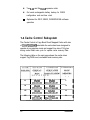
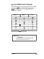
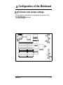
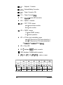
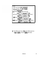
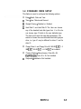
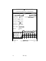
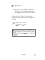
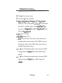
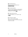
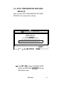
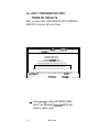
CH-386-33A/40A
User%-Manual
CH=386=33A/4OA
Mainboard
User’s Manual
1 st Edition
Nov 1991
IBM PC/XT/AT/PS2 are registered trademarks of
International Business Machines Corporation
AMI is a trademark of American Megatrends Inc.,
386 is a trademark of Intel Corporation
Opti is a trademark Opti Inc.,
Other brand and product names are trademarks
and/or registered trademarks of their respective companies
Chapter 1
Introduction.
.............................l-1
l-2
Mainboard Specification ..................... l-l
1-3 Cache Control Subsystem ................... l-2
I-4 Local DRAM Control Subsystem .............. I-3
Chapter 2
2I1
Configuration
2-1
. . . . . . . . . . . . . . . . . . . . . . . . . . . .2-l
Connector and Jumper Settings . . . . . . . . . . . . . . . 2-I
Chapter 3
3-1
BIOS Setup ..............................3-l
3-l BIOS Overview. ............................ 3-1
3-2 Standard CMOS Setup ...................... 3-5
3-3 Advanced CMOS Setup ..................... 3-8
3-4
Advanced Chipset Setup .................... 3-12
3-5 Auto Configuration With BIOS Defaults ........ 3-15
3-6 Auto Configuration With Power-On Defaults .... 3-16
3-9
Write To CMOS And Exit .................... 3-l 7
3-10 DoNotWriteToCMOSAndExit..
. . . . . . . . . . . 3-17
1. Introduction
The OPTI- write-back is a highly integrated PC/AT VLSI
chipset, for the high end 386based AT systems, It includes system
controller (SYSC,82C391), Data Buffer controller @BC,82C392)
and integrated peripheral controller (82C206)
l-2 Mainboard Specification
n
33MHz/40MHz 80386 DX CPU
n
80387/WEITEK 3167 Socket on board
n
Coprocessor supports SYNC mode only
n
Copy-Back Direct Mapped Cache with size of
32/64/128/256KB
16 bytes Line size for cache miss cycle
Support 256K/lM/4M DRAM Type
Up to 32MB Local fast page mode DRAM memory space
Supports Two Non-cacheable Regions Control
Shadow RAM support
n
Option for Cacheable video BIOS
Supports Hardware/software switch operation for
Turbo / slow speed.
Supports AT bus clock selectable
Introduction
l-l
n
Two 8bit and Six 16bit expansion slots
n
On board rechargeable battery backup for CMOS
configuration and real-time clock
H
Optimized for OS/Z, XENIX, WINDOWS/386 software
operation
1-3 Cache Control Subsystem
The Cache Control is Copy-Back Direct Mapped Cache with size
of 32/64/l 28/256KB selectable the cache has been designed to
operate at non-pipeline mode and support line size of 16 bytes
during cache Read miss cycle for update cache memory Data.
The following table on the next page shows the cache sizes
support Tag RAM used, cacheable main memory size
L O C A T I O N
I
I
/I
1-2
32
4Kx4bit
U32,U33,U42
8Kx8bit
U34,U35,U36,U37
8
64
4Kx4bit
U32,U33,U42
8Kx8bit
U34-U37, U43-U46
16
128
16Kx4bit
U32,U33,U42
32Kx8bit
U34,U35,U36,U37
32
256
16Kx4bit
U32,U33,U42
32Kx8bit
U34-U37, U43-U46
64
Introduction
I-4 Local DRAM Control Subsystem
This mainboard support 2 bank, page mode local memory, DRAM
devices can be 256K, 1 M or 4M and total memory can be up to
32MB, The following table on the next page illustrates the
configurations supported.
BANK 0
BANK 1
256K
I
256K
I
1M
TOTAL
X
I
1M
256K
I
2M
I
X
I
4M
256K
I
IM
I
5M
1M
I
1M
I
8M
4M
I
X
I
16M
1M
I
20M
I
4M
4M
I
1M
I
20M
4M
I
4M
I
32M
* fast page mode 8017s DRAM is used
* For example f
Fuji MB81256-80 does not support fast page mode
timing, Upon booting the system will appear parity
error message when using the DRAM.
Introduction
l-3
2. Configuration of the Mainboard
2-I Connector and Jumper settings.
The following is a description of jumpers and connectors of the
CH-386-33A/40A mainboard.
I
Jl Jll
I
‘1
l--l
J12
_JlO
cl
I_, UlPl
BTl
80386DX
1
I
I
III
80387
1
I
I
I
-1
r-----lI
Mainboard
JP9
JP8
I
I
I
u
82C392
JP7
JP5ml
-JP6
0 JP3
m
J23
24
SW cn
SW2
2-1
Jl =
Keyboard Connector
JlO=
External Battery Connector
Jll = Power Connector (P8)
J12 = Power Connector (P9)
n
J23 = Keylock & power LED connector
n
J24 = Speaker connector
JPl = CRT TYPE Jumper
open : monochrome monitor
short : color monitor
JP2 = CMOS Jumper
1-2 : clear CMOS memory
2-3 : normal operation
I
2-2
n
JP3 = AT Bus clock selectable jumper
open : AT Bus clock is CPU clock divided by 6
short : AT Bus clock is CPU clock divided by 8
(for 33MHz only, 40MHz always 8MHz)
n
JP4 = Turbo LED
n
SW1 : Hardware REStl switch connector
B
SW2: Hardware TURBO switch connector
n
JP5, JP6, JP7, JP8, JP9, JPIO = cache j u m p e r
64K
I
2-3
I
l-2
I
l-2
1
OPEN
1
2-3
l-2
128K
2-3
l-2
2-3
SHORT
2-3
l-2
256K
2-3
2-3
2-3
SHORT
l-2
1-2
Mainboard
Notes:
Cache even bank: U34,lJ35, U36, U37
Cache odd bank: U43, lJ44,lJ45, U46Tag RAM: U32,- U33, U42
32K cache, put 8Kx6 SRAM at even bank
4/&4 SRAM at U32, U33, and U42
64K cache, put 8ti8 SRAM at both even Ik odd bank,
4Kx4 SRAM at U32, U33, and U42
128K cache, put 32Kx6 SRAM at even bank
76Kx4 SRAM at U32, U33, and U42
256K cache, put 32Kx6 SRAM at both even & odd bank
16Kx4 SRAM at U32, U33, and U42
0 TAG RAM access time is Ens, cache RAM access time
is 25ns for 33MHz or 20ns for 40MHz Main Board.
Mainboard
2-3
3. BIOS SETUP
3-l. BIOS OVERVIEW
The SETUP program is used to configure the system. This
system options are stored in the CMOS. If the CMOS is
good, the system is configured with the values stored in the
CMOS. If the CMOS is bad, the system is configured with
the default values stored in the ROM file.
There are two (2) sets of BIOS values stored in the ROM file :
l
The BIOS Setup defualt values
l
The Power-On default values
The BIOS Setup default values are the default values which
are supposed to give optimum performance for the system.
They are the best case default values.
The Power-On default values are the default values for the
table values for the system. They are the worst case default
values.
BIOS Setup
3-l
There are two ways to enter the BIOS setup program :
l
Whenever BIOS detects any equipment error or the
CMOS contents are not consistent with the equipment.
l
After the power on memory test, the screen will show :
I
Hit c DEL > If you want to run setup
i
- Press the DEL key to get the following screen on
the next page:
3-2
BiOS Setup
BIOS SETUP PROGRAM - AMI BIOS SETUP UTILITIES
(C)1990 American Megatrends Inc., All Rights Reserved
I
II
STANDARD CMOS SETUP
ADVANCED CMOS SETUP
ADVANCED CHIPSET SETUP
AUTO CONFIGURATION WITH BIOS DEFAULTS
AUTO CONFIGURATION WITH POWER-ON DEFAULTS
WRITE TO CMOS AND EXIT
DO NOT WRITE TO CMOS AND EXIT
Standard CMOS Setup for changing Time, Date, Hard disk type, etc.
ESC:Exit
1 - 1+-
: Sel
FZ/F3: Color
FlO:Save & Exit
Explanation of keys :
: Exit to setup program
ESC
: Cursor movement
Arrow keys
: Change Color
F2 / F3
: Save Setup values & Exit to setup program
FlO
BIOS Setup
3-3
The User is given a warning message before he is allowed to
change any of the setup parameters. The warning message
is shown as follows:
BIOS SETUP PROGRAM -WARNING INFORMATION
( C)lQQO American Megatrends Inc., All Rights Reserved
Improper Use of Setup may Cause Problems I!
If System Hangs, Reboot System and Enter Setup by pressing the c ESC > key
Do any of the following After Entering Setup
(i)
Alter options to make system work
(ii) Load BIOS Setup Defaults
(iii) Load Power-On Defaults
.
Hit < ESC > to stop now, Any other key to Continue
:*
- Figure 3 : BIOS Setup Warning Message
Explanation of keys :
: Exit to previous screen
ESC
: Continue choosing setup program
Any keys
3-4
BIOS Setup
3-2. STANDARD CMOS SETUP
This Option is used to configure the following options:
Date : Month, Date and Year.
Et
Time : Hour, Minute and Second.
n Daylight Saving : Disabled or Enabled.
Et
Hard Disk C: and Hard Disk D: The User can choose
any of the standard hard disk types from 1 to 46 or he
can choose type 47 which is the user definable type.
The User must enter the hard disk parameters if he
wants to choose the user-definable hard disk type per
drive, i.e., type 47 may be different for drive C: and for
drive D:.
Floppy Drive A: and Floppy Drive B: 360 KB 5.25, 1.2
MB 5.25, 720 KB 3.5”, 1.44 MB 3.5”, Not Installed.
Primary Display : Monochrome, Color 40 x 25,
VGA/PGA/EGA, Color 80 x 25, Not Installed.
n Keyboard : Installed or Not Installed.
BIOS setup
3-5
BIOS SETUP PROGRAM - STANDARD CMOS SETUP
(C) 1990 American Megatrends Inc., All Rights Resewed
Date (mm/date/year) : Wed,Jun 05,199l
Base memory:640KB
Time (hour/min/sec) : 15 : 35
Ext. memory:7168KB
Daylight Saving
: 50
: Disabled
Cyln Heads WPcom UIone Sect Size
Hard Disk C:Type : Not Installed
Hard Disk D:Type : Not Installed
Floppy Drive A
: 1.2MB, 5.25”
Floppy Drive B
: Not Installed
Primary display
: VGA/PGA/EGA
Keyboard
: Installed
Date:01,02,03,.....31
Year:l901,1902,.....2099
l
ESC: Exit
Sun (Man ITue IWed IThu IFri
26
127 128 I29 130
131
2
3
4
5
6
7
10
11
12
13
14
9
ISat
I1
8
15
16
23
17
1
18
2
19
20
21
22
3
4
5
6
l- -:Sel F2/F3:Color P u / P d : M o d i f y
I=
3-6
BIOS Setup
0 Note : Daylight Saving
- The RTC has a built-in capability to automatically
adjust the time on the two daylight savings days of
the year (*). If this is desired, set the field to “Enable”.
Otherwise, set field to “Disabled”. Note that in general,
nothing will be immediately observable by setting the field to
either state.
l
l
Eg
Daylight Savings.......... Enable
Day&h t Savings.. ....... Disable
* On the last Sunday of April, the time increments from
l-59:59 am to 3:00:00 am. On the last Sunday in October,
when the time first reaches l-59:59 am, it is rolled- back
to 1:OO:OO am.
BIOS Setup
3-7
3-3. ADVANCED CMOS SETUP
The ADVANCED CMOS SETUP option is used to set the
various system options for the user. The User can get
various options, some of which are listed below:
tJ
Numeric Processor Test
n Weitek Processor
~ Cache Memory
a Adaptor ROM Shadow
n Shadow RAM
3-8
BIOS Setup
I
BIOS SEIUP PROGRAM - ADVANCED CMOS SETUP
(C) 1980 American Meaatrends Inc.. Ail Rights Reserved
Numeric Processor Test
Weitek Processor
Cache Memory
Adaptor ROM Shadow C600,16K
Adaptor ROM Shadow CCOO,16K
Adaptor ROM Shadow DOOO,16K
Adaptor ROM Shadow D400,16K
Adaptor ROM Shadow D600,16K
Adaptor ROM Shadow DCOO,l6K
Adaptor ROM Shadow E000,16K
Adaptor ROM Shadow E400,16K
Adaptor ROM Shadow E600,16K
Adaptor ROM Shadow ECOO,16K
Shadow RAM Option
~
ESC:Exit
F5:Oid Values
4+t+
I
: Disabled 11
: Absent
: Enabled
: Disabled
: Disabled
: Disabled
: Disabled
: Disabled
: Disabled
: Disabled
: Disabled
: Disabled
: Disabled
: Both
)
( C t r i Pu/Pd:Modify
:Sei
F6:BiOS Setup Defaults
BIOS Setup
F2/F3:Coior
Fl :Heip
F7:Power-On Defaults
3-9
Explanation of keys
l
ESC : Exit to previous screen
l
Arrow keys : Cursor movement
a PageUp / PageDown / Ctrl PageUp / Ctrl PageDown :
Modify the value of the option by l/-1/10/-10. If the option
has less than 10 available answers, then < Ctrl PageUp >
is the same as < PageUp > and < Ctrl PageDown > is
the same as < PageDown >.
l
Fl :
l
F2 / F3 : Change Color
l
F5 : Get the old values. These are values with the user
Option for Help
starting from the current session. If the CMOS was good,
then the old values are the CMOS values, hense they are
the BIOS Setup default values.
F6 : This will load all the options in the Advanced CMOS
Setup / Advanced Chipset Setup with the BIOS setup
defaults
F7 : This will load all the options in the Advanced CMOS
Setup / Advanced Chipset Setup with the Power-On
defaults
3-10
BIOS Setup
Cl Numeric Processor Test
INTEL Coprocessor insert in socket, Enable is set.
When not inserted, Disable is set.
0 WEITExK Processor
WEITEK coprocessor insert in socket, present is set.
When not inserted in socket, absent is set.
0 Cache Memory
This function can be setup Enable/Disable External Cache
32/64/l 28/256KB.
0 Adaptor RAM Shadow
Adaptor Shadow RAM address range from C8000H to
EFFFFH, each block size at the 16KB for Enable or Disable
0 Shadow RAM
There are four functions that can be selected:
Video
Main
Both
Disable
: Video shadow ( COO00 - C7FFFH )
: Main BIOS shadow ( FOOOO cv FFFFFH )
: Video and Main BIOS shadow
: Disable shadow
BIOS Setup
3-11
3-4. ADVANCED CHIPSET SETUP
The ADVANCED CHIPSET SETUP option is used to change
the register values for the chipset registers. The chipset
registers control most of the system options in the computer.
(C) 1 QQO American
M - ADVANCED CMOS SETUP
Inc., All Rights Reserved
Non-Cacheable block-l Base
: Disabled
Non-Cacheable block-l Size
Non-Cacheable block-2 Base
Non-Cacheable block-2 Size
:oKB
Disabled
:
Cacheable RAM Address Range
Video BIOS Area Cacheable
I ’
l=i
3-12
ESC:Exit
F&Old value
4*
t
:oKB
:8MB
: Yes
ct Sel (Ctrl)Pu/Pd:Modify
F&BIOS Setup Defaults
BIOS Setup
Fl:Help F2/F3:Color
F7:Power-on Defaults
Explanation of keys
:
ESC : Exit to previous screen
Arrow keys : Cursor movement
PageUp / PageDown / Ctrl PageUp / Ctrl PageDown :
Modify the value of the option l/-1/10/-10. If the option has
less than 10 available answers, then < Ctrl PageUp > is
the same as < PageUp > and < Ctrl PageDown > is the
same as < pageDown >
Fl :
Option for Help
F2 / F3 : Change Color
F5 : Get the old values. This are the values with the user
starting from the current session. If the CMOS was good,
then the old values are the CMOS values, hence they are
the BIOS Setup default values.
F6 : This will load all the options in the Advanced CMOS
Setup / Advanced Chipset Setup with the BIOS Setup
defaults
F7 : This will load all the options in the Advanced CMOS
Setup / Advanced Chipset Setup with the Power-On
BIOS Setup
3-13
0 Non-Cacheable Block Size
This setup for set Non-Cacheable block size of
64/l 28/256/S 2K/Disable
0 Non-Cacheable Block Base
This setup for set Non-Cacheable block starting address for
example, if a 512KB non-cacheable block is selected, its
starting address is a multiple of 512KB
0 Cacheable RAM Address Range
This Cacheable DRAM size, you can select from range
(1064MB)
0 Video BIOS Area Cacheable
Enable or Disable Video BIOS Cacheable
Please check you VGA card, If OAK VGA card (slow speed),
this function must disable
3-14
BIOS Setup
3-5. AUTO CONFIGURATION WITH BIOS
DEFAULTS
When you enter AUTO CONFIGURATION WITH BIOS
DEFAULTS, the screen will be as follows:
-
BIOS SETUP PROGRAM AMI BIOS SETUP UTILITIES
(C) 1990 American Megatrends Inc., All Rights Reserved
STANDARD CMOS SETUP
ADVANCED CMOS SETUP
ADVANCED CHIPSET SETUP
AUTO CONFIGURATION WITH BIOS DEFAULTS
AUTO CONFIGURATION WITH POWER-ON DEFAULTS
Load BIOS Setup Default Values from ROM Table (Y/N) ? N
Load BIOS Setup Defaullt Values for Advanced CMOS and Advanced CHIPSET Setup
ESC:Exit
1 -+ 7 * :Sel
F2/F3:Color
FlO:Save & Exit
- Press “yl’ or “N” to change ADVANCED CMOS
SETUP and ADVANCED CHIPSET SETUP with
BIOS default values.
BIOS Setup
3-15
3-6. AUTO CONFIGURATION WITH
POWER-ON DEFAULTS.
When you enter AUTO CONFIGURATION WITH POWER-ON
DEFAULTS, the screen will be as follows:
-
BIOS SETUP PROGRAM AMI BIOS SETUP UTIUTIES
(C) 1990 Am&an Megatrends Inc., All Rights Reserved
STANDARD CMOS SETUP
ADVANCED CMOS SETUP
ADVANCED CHIPSET SETUP
AUTO CONFIGURATION WITH BIOS DEFAULTS
AUTO CONFIGURATION WITH POWER-ON DEFAULTS
Load Power-On Default Values from ROM Table (Y/N) ? N
Default Values for Advanced CMOS and Advanced CHIPSET Setup
F2/F3:Color
F10:Save & Exit
- Press “Y” or “N” to change ADVANCED CMOS
SETUP and ADVANCED CHIPSET SETUP with
Power-On default values.
3-16
BIOS Setup
3-9. WRITE TO CMOS AND EXIT
The options set in the Standard Setup, Advanced Setup,
Advanced Chipset Setup and the New password ( If it has
been changed ) are stored in the CMOS. The CMOS
checksum is calculated and writtten into the CMOS. After
that, control is passed back to the BIOS.
3-10. DO NOT WRITE TO CMOS AND EXIT
Control is passed back to the BIOS without writing to the
CMOS.
BIOS Setup
3-17