1
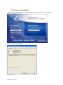
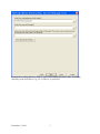
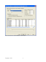
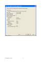
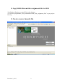
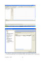
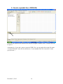
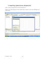
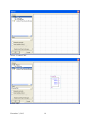
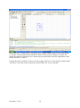
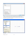
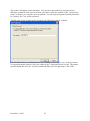
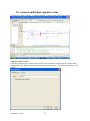
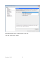
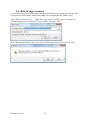
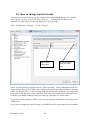
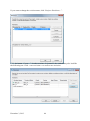
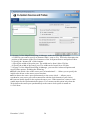
Tutorial for Altera DE1 and Quartus II
Qin-Zhong Ye
December, 2013
This tutorial teaches you the basic steps to use Quartus II version 13.0 to program Altera’s
FPGA, Cyclone II EP2C20 on the Development & Education Board DE1. One can also use it
as a simplified user manual.
Some screen prints are taken from Quartus II version 9 and therefore may be slightly different
from that of Quartus II version 13.0.
Contents
1.
Create a new project ............................................................................................................ 2
2.
Copy VHDL files and the assignment file for DE1 ............................................................ 9
3.
Create a new schematic file ................................................................................................ 9
4.
Open an existing VHDL file and add it to a project ......................................................... 13
5.
Create a symbol for a VHDL file ...................................................................................... 16
6.
Importing symbols to the schematic file ........................................................................... 18
7.
Importing assignments ...................................................................................................... 21
8.
Importing input and output symbols ................................................................................. 23
9.
Connect symbols in a schematic ....................................................................................... 26
10. Connect individual signals to a bus .................................................................................. 27
11. Specify the unused pins setting ......................................................................................... 30
12. Compilation....................................................................................................................... 33
13. Programming FPGA Chip ................................................................................................. 34
14. Viewing implementation logic .......................................................................................... 36
15. Checking the problem with pin assignment ...................................................................... 37
16. How to update a symbol after making changes to signal names ...................................... 39
17. What to do after add/remove input/output signals in a VHDL file ................................... 41
18. How to create a VHDL file for the schematic file ............................................................ 42
19. How to copy a project ....................................................................................................... 43
20. How to change top-level entity ......................................................................................... 44
21. How to change revision name ........................................................................................... 45
22. How to use In-System Sources and Probes Editor ............................................................ 48
23. How to install USB driver................................................................................................. 54
December 3, 2013
1
1. Create a new project
(Notice that you should create a working directory in the local disk (e.g., D:\) of the PC
before creating a new project.)
Click ”Create a New Project”.
Click ”Next”.
December 3, 2013
2
Change the working directory name to your own working directory name. A working
directory in the local drive (e.g., D:\) of the PC is preferred.
December 3, 2013
3
Fill in the name of your project. Click “Next”.
Click ”Ja”.
December 3, 2013
4
If there is no design file (e.g. schematic or VHDL files) to add, click “Next”.
December 3, 2013
5
If the selected device is EP2C20F484C7, click “Next”.
December 3, 2013
6
Click “Next”.
December 3, 2013
7
Click “Finish”.
December 3, 2013
8
2. Copy VHDL files and the assignment file for DE1
Use Windows Explorer to copy all files in the directory
“S:\TN\E\094_Digitalteknik_och_konstruktion\VHDL_and_assignment_files” to your project
directory.
3. Create a new schematic file
Select “File > New …”
December 3, 2013
9
Select “BlockDiagram/Schematic File” and click “OK”.
December 3, 2013
10
Select “File > Save as …” to change the file name to a new name. This file name of the
schematic will be used as the “top-level design entity” name of your whole design. You
should choose the same name as the name of “top-level design entity”. However, please
notice that the file name for the schematic cannot be the same as any entity name in the
VHDL codes.
December 3, 2013
11
Click “Spara”. Notice that the file name “Counter_example” should be the same as the “toplevel design entity” name.
December 3, 2013
12
4. Open an existing VHDL file and add it to a project
Select “File > Open…”. Find the VHDL file and click “Öppna”.
Notice that you should have already copied all files in the directory
“S:\TN\E\094_Digitalteknik_och_konstruktion\VHDL_and_assignment_files” to your project
directory.
December 3, 2013
13
Select “Project > Add/Remove Files in Project …” in the main toolbar.
Click “Add All”. (Notice that you should have already copied all files in the directory
“S:\TN\E\094_Digitalteknik_och_konstruktion\VHDL_and_assignment_files” to your project
December 3, 2013
14
directory.) (Alternatively, you can also click “…” and navigate to your project directory and
find the VHDL files.)
The list shows that two VHDL files are added to your project. Click “OK”.
December 3, 2013
15
5. Create a symbol for a VHDL file
Click the file symbol at the bottom of the Project Navigator. Double-click “Counter27bit.vhd”
to open it.
(Alternatively, if you don’t want to open the VHDL file, you can right-click on the file name
“Counter27bit.vhd” in the file list and choose “Create Symbol files for Current file” in the
pop-up menu.)
December 3, 2013
16
Select “Processing > Analyze Current File”.
Click “OK”.
Click “File > Create/Update > Create Symbol Files for Current File”.
Click “OK”.
Perform the same operations (i.e., open file, analyze file, create symbol files) as above for the
VHDL file “Seven_seg.vhd”.
December 3, 2013
17
6. Importing symbols to the schematic file
Click “Counter_example.bdf” to view the schematic file.
Double-click on the blank space of the Graphic Editor window or click on the AND-gate icon
in the toolbar.
Click the “+” sign to expand “Project” in the Libraries box.
December 3, 2013
18
Select “Counter27bit”.
Click “OK”.
December 3, 2013
19
The symbol for “Counter27bit” will appear in the Graphic Editor window. Move the symbol
to a proper location and click the left mouse button. If the symbol continues to follow the
mouse movement, click on the “Esc” button on your keyboard or click the right button of the
mouse and select “Cancel”.
Perform the same operations as above for the symbol “bcd7seg”. Notice that the symbol name
“bcd7seg” is the same as the entity name in the VHDL file “seven_seg.vhd”.
December 3, 2013
20
7. Importing assignments
You should use the assignment file “DE1_pin_assignments.csv” for your project. In this
assignment file, input and output signal names are assigned to the pins of FPGA. These pins
of FPGA are connected to various components on the printed circuit board. Click
“Assignments > Import Assignments …” in the main toolbar.
Click “…” to find the assignment file.
December 3, 2013
21
Click “Öppna”.
Click “OK”.
December 3, 2013
22
Click “Assignments > Pin Planner” in the main toolbar.
The content of the assignment file is shown in the lower part of the window. If you want to
connect the output signals of the 7-segment decoder to the input signals of a 7-segment
display on DE1, you should use the pre-defined output signal names in the Node Name
column of the assignment editor. For example, HEX0[0], HEX0[1], … HEX0[6] are the 7
output signals of the right-most 7-segment display on DE1. The input pins of the display are
connected to 7 output pins of the FPGA chip. For each pre-defined signal name, you can find
the corresponding pin of the FPGA chip in the column “Location”. The 50 MHz oscillator on
DE1 has a pre-defined input signal name CLOCK_50 and it is connected to the pin “PIN_L1”
of the FPGA chip.
8. Importing input and output symbols
Double-click on the blank space of the Graphic Editor window or click on the AND-gate icon
in the toolbar.
December 3, 2013
23
Click the “+” sign to expand “c:/altera/13.0/quartus/libraries” in the Libraries box. You can
expand the hierarchy as show in the follow window to find input and output symbols.
(Notice that you can also find the instructions for importing input and output symbols as in
the tutorial “tut_quartus_intro_schem.pdf”.)
Click “OK”.
December 3, 2013
24
The symbol will appear in the schematic. You can move the symbol by using the mouse.
When the symbol is at the correct position, left-click to place the symbol. If the “repeat insert
mode” is chosen, you can place several symbols. You can stop the repeated symbol placement
by clicking “Esc” key on the keyboard.
Double-click on the symbol in the schematic, the following window is shown.
You should use these pre-defined names (e.g., HEX0[0], CLOCK_50, etc.) as the pin names
for input and output symbols. Since the output of the 7-segment decoder is a bus. The output
symbol should also be a bus. Use the notation HEX0[0..6] as the pin name. Click “OK”.
December 3, 2013
25
9. Connect symbols in a schematic
Click “Orthogonal Node Tool” (for a single signal) in the toolbar. Use the tool to connect the
input CLOCK_50 to the Clk input of Counter27bit.
Click “Orthogonal Bus Tool” (for a bus) in the toolbar. Use the tool to connect the output of
the decoder to the output symbol.
December 3, 2013
26
10. Connect individual signals to a bus
Connect the counter and the 7-segment decoder as shown in the following window.
Assign a name to a bus
Click the selection tool (Arrow) in the toolbar. Select the bus connected to the input of the 7segment decoder. Right-click on the bus and select “Properties”. The following window will
appear.
December 3, 2013
27
Fill in a bus name (any name you like). Click “OK”.
Assign a name to a node (signal) line
Click the selection tool (Arrow) in the toolbar. Select the node (signal) line connected to the
output of the counter. Right-click on the line and select “Properties”. The following window
will appear.
Fill in a node (signal) line name which is connected to a single bit of the connected bus. For
the output signal “clkbit26”, the node line name is b[3]. Click “OK”.
Assign node line names to the other 3 lines. The result is shown in the following window.
Save the file.
December 3, 2013
28
December 3, 2013
29
11. Specify the unused pins setting
Click “Assignments > Device …” in the main toolbar, the “Device” window is shown.
Click “Device and Pin Option…” icon.
December 3, 2013
30
Select “Unused Pins” in “Category”
December 3, 2013
31
In the pull-down menu, select “As input tri-stated”. Click “OK”.
Click “OK” in the “Device” window.
December 3, 2013
32
12. Compilation
Click “Processing > Start Compilation”.
If the compilation is successful, the following window is displayed.
The large number of warnings is due to the unused node names in the assignment file.
Click “Assignments > Pins” in the main menu. Observe that the used pins are moved to the
top of the list as shown in the following window.
December 3, 2013
33
13. Programming FPGA Chip
Check whether the AC/DC adapter and the USB cable are connected. Turn on the power of
DE1 by pushing the red button on DE1.
Click “Tools > Programmer” in the main toolbar.
Make sure the Mode is “JTAG”. Click “Start”. If “Start” is not clickable, as shown in the
following window, click “Hardware Setup…”.
December 3, 2013
34
Click “Hardware Setup…” at the upper-left corner of the window.
In the pull-down menu for “Currently selected hardware”, select “USB-Blaster[USB-0]”.
Click “Close”. Now “Start” should be clickable. (Notice that USB driver for DE1 should
have been installed. If it is not installed, follow the instructions in chapter 22, How to install
USB driver.)
December 3, 2013
35
14. Viewing implementation logic
Click “Tools > Netlist Viewers > RTL Viewer”.
Double click the symbols to expand “counter27bit” and “bcd7seg” to view details.
December 3, 2013
36
Chapters 15 – 23 are not tutorial steps and may be used as a
simple user manual.
15. Checking the problem with pin assignment
Note that this chapter is not a tutorial step. When you are looking for the reasons why you
circuit does not work, you may need to read this chapter and check whether you have a
problem with pin assignment.
One problem with the pin assignment in Quartus II version 13.0 is the setting for “Block
Design Naming”. After compilation of your schematic and VHDL codes with the schematic
as the top-level design entity, you should find the names of the input and output signals which
you have used in the schematic at the top of the node name list in Pin Planner. If you find that
there are other signal names which are added into the node name list, it is an indication that
the setting for “Block Design Naming” is causing a problem for the compilation. The
synthesized circuit may not work properly. The in-system sources and probes may also be
affected by this problem.
You can correct the setting for “Block Design Naming” as follows.
Click on “Assignment > Settings…” in the main toolbar, the following window is shown.
December 3, 2013
37
Click on “Analysis & Synthesis Settings” and the click on “More settings…” button. The
following window is shown.
Double-click on “Auto” of the setting ”Block Design Naming”. The pull-down menu will
show 3 alternatives. Select “Quartus II” and click “OK” to close the window.
Compile your project again and check whether the synthesized circuit works. Note that the
added names in the node name list might still be there in “Pin Planner”. But they are not
causing the problem. (If you notice any problems or errors with this part of text, please let me
know.)
December 3, 2013
38
16. How to update a symbol after making changes to
signal names
If you change the names of any input/output signals in a VHDL file, you should do the
following steps:
Click “Processing > Analyze Current File” to check the modified VHDL code.
View the schematic in Graphic Editor. Right-click on the symbol.
Select “Edit Selected Symbol” from the pull-down menu.
December 3, 2013
39
Change the names of the signals
Double-click on the name of the signal.
Change the signal name and click “OK”. Save the file.
December 3, 2013
40
Update symbols
Right-click in the blank space of the Graphic Editor and click “Update Symbol or Block…”.
Click “OK”.
17. What to do after add/remove input/output signals in
a VHDL file
If you add/remove input/output signals in a VHDL file, you should create the symbol again by
clicking “File > Create/Update > Create Symbol Files for Current File” and adding the new
symbol to the schematic file.
December 3, 2013
41
18. How to create a VHDL file for the schematic file
Click “File > Create/Update > Create HDL Design File for Current File”.
Click “OK”.
Notice that the created file is not added in the project since this file is not needed for
compilation of your design. The VHDL file is useful if you want to move your design to
another design tool or software.
If you want to view it, you can open this file by clicking “File > Open…”.
Select the VHDL file “counter_example” and click “Öppna”.
The code is an example of the structural style VHDL code. There are 2 components,
“bcd7seg” and “counter27bit”, in the code.
December 3, 2013
42
19. How to copy a project
It is possible to copy an existing project and give the copied project a new project name. The
copied project can be further improved by adding new components and VHDL codes.
Click “Project->Project copy…”. When the “Copy Project” window pops up, change the
“Destination directory” and the “New project name” and click “OK”.
If the “Destination directory” does not exist, the following window pops up. Click “Yes”.
December 3, 2013
43
20. How to change top-level entity
Sometimes, you need to change top-level entity before compiling the design. For example,
after copying a project, if you click “File->Save As…” to change the file name of the
schematic to a new name, you need to change the top-level entity.
Click “Assignments-> Settings…”. Click “General”.
Type a new
entity name
Select an entity
from an entity
list
Select an entity from the pull-down list for “Top-level entity”. Some entity names in the list
are the entity names in the VHDL codes. (Notice that entity names may be different from the
VHDL file names!) There is also an entity name for the schematic in the list. The entity name
is the same as the file name of the schematic. If the new entity name for the schematic is not
in the list, you should change the top-level entity by typing the new entity name.
If you only want to compile a VHDL code, you can select the entity name of the entity in the
VHDL code.
If you want to compile the whole design, you should select the entity name for the schematic.
December 3, 2013
44
21. How to change revision name
A revision name is used to set the output file names after compilation.
Revision name
For example, the revision name is used as the name of the file to be downloaded into FPGA.
December 3, 2013
45
If you want to change the revision name, click “Project->Revisions…”.
Click the button “Create…”. In other versions of Quartus II, the window may also look like
the following one. Click <<new revision>> to create a new revirsion.
December 3, 2013
46
Fill in a new revision name and click “OK”.
Click “OK”.
Notice that, in the above window, if you want to delete the old revision, you can click the
revision name in the list and click the button “Delete”. All the output files of the revision will
be deleted.
December 3, 2013
47
22. How to use In-System Sources and Probes Editor
The In-System Sources and Probes Editor in the Quartus II software allows you to easily
control any internal signal and provides you with a completely dynamic debugging
environment. You can get more information on the In-System Sources and Probes Editor from
the Quartus II Handbook, Chapter 16 (Volume 3: Verification, Section IV: System Debugging
Tools).
The In-System Sources and Probes Editor consists of the ALTSOURCE_PROBE
megafunction and an interface to control the ALTSOURCE_PROBE megafunction instances
during run time. Each ALTSOURCE_PROBE megafunction instance provides you with
source output ports and probe input ports, where source ports drive selected signals and probe
ports sample selected signals. When you compile your design, the ALTSOURCE_PROBE
megafunction sets up a register chain to either drive or sample the selected nodes in your logic
design. During run time, the In-System Sources and Probes Editor uses a JTAG connection to
shift data to and from the ALTSOURCE_PROBE megafunction instances.
Configuring the ALTSOURCE_PROBE Megafunction
To use the In-System Sources and Probes Editor in your design, you must first instantiate the
ALTSOURCE_PROBE megafunction variation file. You can configure the
ALTSOURCE_PROBE megafunction with the MegaWizard™ Plug-In Manager.
Each source or probe port can be up to 256 bits. You can have up to 128 instances of the
ALTSOURCE_PROBE megafunction in your design.
To configure the ALTSOURCE_PROBE megafunction, performing the following steps:
1. On the Tools menu, click MegaWizard Plug-In Manager.
2. Select Create a new custom megafunction variation.
December 3, 2013
48
3. Click Next.
4. On page 2a of the MegaWizard Plug-In Manager, make the following selections:
a. In the Installed Plug-Ins list, expand the JTAG-accessible Extensions folder and select InSystem Sources and Probes. (You can also verify that the currently selected device family
matches the device you are targeting.)
b. Select an output file type and enter the name (for example, source_probe1) of the
ALTSOURCE_PROBE
megafunction. You can choose AHDL (.tdf), VHDL (.vhd), or Verilog HDL (.v) as the
output file type.
5. Click Next.
December 3, 2013
49
6. On page 3 of the MegaWizard Plug-In Manager, make the following selections:
a. Under Do you want to specify an Instance Index?, turn on Yes. This index determines the
position of the instance in the list of instances of the In-System Sources and probes Editor.
b. Specify the ‘Instance ID’ of this instance.
c. Specify the width of the probe port. The width can be from 0 bit to 256 bits.
d. Specify the width of the source port. The width can be from 0 bit to 256 bits.
7. On page 3 of the MegaWizard Plug-In Manager, you can click Advanced Options and
specify other options, including the following:
■ What is the initial value of the source port, in hexadecimal? — Allows you to specify the
initial value driven on the source port at run time.
■ Write data to the source port synchronously to the source clock — Allows you to
synchronize your source port write transactions with the clock domain of your choice.
■ Create an enable signal for the registered source port—When turned on, creates a clock
enable input for the synchronization registers. You can turn on this option only when the
Write data to the source port synchronously to the source clock option is turned on.
8. Click Next.
December 3, 2013
50
9. Click Next.
10. Select (tick) soure_probe1.bsf to create a Quartus II symbol file. The symbol can be
imported to the schematic of your design. (Sinec the file “source_probe1.vhd” is always
created, you can also create the symbol for the VHDL file. See Chapter 5, Create a symbol for
a VHDL file,”, of this document.)
11. Click Finish.
December 3, 2013
51
12. Click Yes.
Import the created symbol to the schematic of your project
Follow the instructions in Chapter 6, Importing symbols to the schematic file, of this
document.
Compile the project
Click “Processing > Start Compilation”. See Chapter 12, Compilation, of this document.
Program FPGA Chip
Click “Tools > Programmer”. See Chapter 13, Programming FPGA Chip, of this document.
Running the In-System Sources and Probes Editor
1. Open the In-System Sources and Probes Editor. Click “Tools >In-System Sources and
Probes Editor”.
If you have not programed FPGA chip, you should do Steps 2 - 5 to program FPGA chip.
Otherwise, you can skip Steps 2– 5.
2. In the JTAG Chain Configuration pane, point to Hardware, and then select the hardware
communications device. You may be prompted to configure your hardware; in this case, click
Setup.
3. From the Device list, select the FPGA device to which you want to download the design
(the device may be automatically detected). You may need to click Scan
Chain to detect your target device.
4. In the JTAG Chain Configuration pane, click to browse for the SRAM Object File
(.sof) that includes the In-System Sources and Probes instance or instances. (The
.sof may be automatically detected).
5. Click Program Device to program the target device.
Instance Manager
The Instance Manager pane provides a list of all ALTSOURCE_PROBE instances in the
design and allows you to configure how data is acquired from or written to those instances.
The following buttons and sub-panes are provided in the Instance Manager pane:
■ Read Probe Data—Samples the probe data in the selected instance and displays the probe
data in the In-System Sources and Probes Editor pane.
■ Continuously Read Probe Data—Continuously samples the probe data of the selected
instance and displays the probe data in the In-System Sources and
Probes Editor pane; you can modify the sample rate via the Probe read interval setting.
December 3, 2013
52
■ Stop Continuously Reading Probe Data—Cancels continuous sampling of the probe of the
selected instance.
■ Write Source Data—Writes data to all source nodes of the selected instance.
■ Probe Read Interval—Displays the sample interval of all the In-System Sources and Probe
instances in your design; you can modify the sample interval by clicking Manual.
■ Event Log—Controls the event log in the In-System Sources and Probes Editor pane.
■ Write Source Data—Allows you to manually or continuously write data to the system.
The status of each instance is also displayed beside each entry in the Instance Manager pane.
The status indicates if the instance is Not running Offloading data, Updating data, or if an
Unexpected JTAG communication error occurs. This status indicator provides information
about the sources and probes instances in your design.
In-System Sources and Probes Editor Pane
The In-System Sources and Probes Editor pane allows you to view data from all sources and
probes in your design. The data is organized according to the index number of the instance.
The editor provides an easy way to manage your signals, and allows you to rename signals or
group them into buses. All data collected from in-system source and probe nodes is recorded
in the event log and you can view the data as a timing diagram.
Reading Probe Data
You can read data by selecting the ALTSOURCE_PROBE instance in the Instance Manager
pane and clicking Read Probe Data. This action produces a single sample of the probe data
and updates the data column of the selected index in the In-System
Sources and Probes Editor pane. You can save the data to an event log by turning on the Save
data to event log option in the Instance Manager pane.
If you want to sample data from your probe instance continuously, in the Instance Manager
pane, click the instance you want to read, and then click Continuously read probe data. While
reading, the status of the active instance shows Unloading. You can read continuously from
multiple instances.
You can access read data with the shortcut menus in the Instance Manager pane.
To adjust the probe read interval, in the Instance Manager pane, turn on the Manual option in
the Probe read interval sub-pane, and specify the sample rate in the text field next to the
Manual option. The maximum sample rate depends on your computer setup. The actual
sample rate is shown in the Current interval box. You can adjust the event log window buffer
size in the Maximum Size box.
Writing Data
To modify the source data you want to write into the ALTSOURCE_PROBE instance, click
the name field of the signal you want to change. For buses of signals, you can double-click the
data field and type the value you want to drive out to the ALTSOURCE_PROBE instance.
The In-System Sources and Probes Editor stores the modified source data values in a
temporary buffer. Modified values that are not written out to the ALTSOURCE_PROBE
instances appear in red. To update the ALTSOURCE_PROBE instance, highlight the instance
in the Instance Manager pane and click Write source data. The Write source data function is
also available via the shortcut menus in the Instance Manager pane.
The In-System Sources and Probes Editor provides the option to continuously update each
ALTSOURCE_PROBE instance. Continuous updating allows any modifications you make to
the source data buffer to also write immediately to the ALTSOURCE_PROBE instances. To
continuously update the ALTSOURCE_PROBE instances, change the Write source data field
from Manually to Continuously.
December 3, 2013
53
Organizing Data
The In-System Sources and Probes Editor pane allows you to group signals into buses, and
also allows you to modify the display options of the data buffer.
To create a group of signals, select the node names you want to group, right-click and select
Group. You can modify the display format in the Bus Display Format and the
Bus Bit order shortcut menus.
The In-System Sources and Probes Editor pane allows you to rename any signal. To rename a
signal, double-click the name of the signal and type the new name.
The event log contains a record of the most recent samples. The buffer size is adjustable up to
128k samples. The time stamp for each sample is logged and is displayed above the event log
of the active instance as you move your pointer over the data samples.
You can save the changes that you make and the recorded data to a Sources and Probes File
(.spf). To save changes, on the File menu, click Save. The file contains all the modifications
you made to the signal groups, as well as the current data event log.
23. How to install USB driver
USB blaster is the USB device on Altera’s FPGA board, DE1. When DE1 is connected to a
PC through a USB cable, the USB driver for USB Blaster should be installed. The USB driver
can be found in the folder “\altera\91sp2\quartus\drivers\usb-blaster”, if Quartus II version 9.1
is installed on the PC.
When DE1 is connected to a PC with Windows XP, a pop-up window “Found New
Hardware Wizard” will be shown to guide the installation of the driver. See the details in the
manual “Getting started with Altera DE1.pdf”.
When DE1 is connected to a PC with Windows Vista, a pop-up window will be shown to
guide the installation of the driver. Similar steps as for Windows XP should be done.
When DE1 is connected to a PC with Windows 7, no pop-up window will be shown. One
should follow the following steps in “Manual for installation of Quartus II and USB driver for
Windows 7” in “Manual_install_Quartus_USBdriver_Windows_7.pdf” to install the USB
driver.
December 3, 2013
54