1
External Memory PHY Interface (ALTMEMPHY)
(nonAFI) Megafunction User Guide
101 Innovation Drive
San Jose, CA 95134
www.altera.com
UG-01014-7.3
Software Version:
Document Version:
Document Date:
9.1 SP1
7.3
January 2010
Copyright © 2010 Altera Corporation. All rights reserved. Altera, The Programmable Solutions Company, the stylized Altera logo, specific device designations, and all other words
and logos that are identified as trademarks and/or service marks are, unless noted otherwise, the trademarks and service marks of Altera Corporation in the U.S. and other countries. All other product or service names are the property of their respective holders. Altera products are protected under numerous U.S. and foreign patents and pending
applications, maskwork rights, and copyrights. Altera warrants performance of its semiconductor products to current specifications in accordance with Altera's standard warranty, but reserves the right to make changes to any products and services at any time without notice. Altera assumes no responsibility or liability arising out of the application or use
of any information, product, or service described herein except as expressly agreed to in writing by Altera Corporation. Altera customers are advised to obtain the latest version of
device specifications before relying on any published information and before placing orders for products or services.
Contents
Chapter 1. About this Megafunction
Chapter 2. Parameter Settings
Memory Settings . . . . . . . . . . . . . . . . . . . . . . . . . . . . . . . . . . . . . . . . . . . . . . . . . . . . . . . . . . . . . . . . . . . . . . 2–2
Use the Preset Editor to Create a Custom Memory Preset . . . . . . . . . . . . . . . . . . . . . . . . . . . . . . . . 2–4
Creating an Emulated x36 QDR II+/QDR II SRAM ALTMEMPHY Variation . . . . . . . . . . . . . . . . . 2–7
Chapter 3. Functional Description—ALTMEMPHY (nonAFI)
QDR II+/QDR II SRAM Calibration Process . . . . . . . . . . . . . . . . . . . . . . . . . . . . . . . . . . . . . . . . . . . . . . . . 3–1
PHY-to-Controller Interfaces . . . . . . . . . . . . . . . . . . . . . . . . . . . . . . . . . . . . . . . . . . . . . . . . . . . . . . . . . . . . . . 3–4
Initialization Timing . . . . . . . . . . . . . . . . . . . . . . . . . . . . . . . . . . . . . . . . . . . . . . . . . . . . . . . . . . . . . . . . . . . . . 3–5
DDR SDRAM Initialization Timing . . . . . . . . . . . . . . . . . . . . . . . . . . . . . . . . . . . . . . . . . . . . . . . . . . . 3–5
DDR2 SDRAM Initialization Timing . . . . . . . . . . . . . . . . . . . . . . . . . . . . . . . . . . . . . . . . . . . . . . . . . . 3–7
ALTMEMPHY Signals . . . . . . . . . . . . . . . . . . . . . . . . . . . . . . . . . . . . . . . . . . . . . . . . . . . . . . . . . . . . . . . . . . . 3–9
DDR2 and DDR SDRAM Signals . . . . . . . . . . . . . . . . . . . . . . . . . . . . . . . . . . . . . . . . . . . . . . . . . . . . . . . . 3–9
QDR II+/QDR II SRAM Signals . . . . . . . . . . . . . . . . . . . . . . . . . . . . . . . . . . . . . . . . . . . . . . . . . . . . . . . . 3–20
Understanding the Testbench . . . . . . . . . . . . . . . . . . . . . . . . . . . . . . . . . . . . . . . . . . . . . . . . . . . . . . . . . . . . 3–25
PLL Initialization and Lock . . . . . . . . . . . . . . . . . . . . . . . . . . . . . . . . . . . . . . . . . . . . . . . . . . . . . . . . . . . . 3–25
Memory Device Initialization . . . . . . . . . . . . . . . . . . . . . . . . . . . . . . . . . . . . . . . . . . . . . . . . . . . . . . . . . . 3–25
Interface Training and Calibration . . . . . . . . . . . . . . . . . . . . . . . . . . . . . . . . . . . . . . . . . . . . . . . . . . . . . . 3–25
Write Training Data . . . . . . . . . . . . . . . . . . . . . . . . . . . . . . . . . . . . . . . . . . . . . . . . . . . . . . . . . . . . . . . . 3–26
Calibration . . . . . . . . . . . . . . . . . . . . . . . . . . . . . . . . . . . . . . . . . . . . . . . . . . . . . . . . . . . . . . . . . . . . . . . 3–26
Functional Memory Use . . . . . . . . . . . . . . . . . . . . . . . . . . . . . . . . . . . . . . . . . . . . . . . . . . . . . . . . . . . . . . 3–26
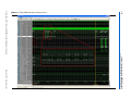
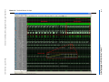
Functional Simulation—the ModelSim Wave and Transcript Window . . . . . . . . . . . . . . . . . . . . . . . . . 3–27
Full Window Stage Identification . . . . . . . . . . . . . . . . . . . . . . . . . . . . . . . . . . . . . . . . . . . . . . . . . . . . . . 3–27
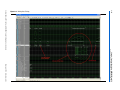
Initialization Stage . . . . . . . . . . . . . . . . . . . . . . . . . . . . . . . . . . . . . . . . . . . . . . . . . . . . . . . . . . . . . . . . . . . 3–29
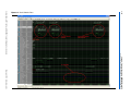
Write Training Data Stage . . . . . . . . . . . . . . . . . . . . . . . . . . . . . . . . . . . . . . . . . . . . . . . . . . . . . . . . . . . . . 3–31
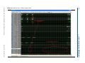
Read Calibration Phase . . . . . . . . . . . . . . . . . . . . . . . . . . . . . . . . . . . . . . . . . . . . . . . . . . . . . . . . . . . . . . . 3–33
Functional Memory Use Stage . . . . . . . . . . . . . . . . . . . . . . . . . . . . . . . . . . . . . . . . . . . . . . . . . . . . . . . . . 3–37
Additional Debug Signals . . . . . . . . . . . . . . . . . . . . . . . . . . . . . . . . . . . . . . . . . . . . . . . . . . . . . . . . . . . . . . . 3–39
PLL and PLL Reconfiguration Signals . . . . . . . . . . . . . . . . . . . . . . . . . . . . . . . . . . . . . . . . . . . . . . . . . . 3–39
Calibration Status Interface . . . . . . . . . . . . . . . . . . . . . . . . . . . . . . . . . . . . . . . . . . . . . . . . . . . . . . . . . . . . 3–40
Additional Calibration Status Interface Signals . . . . . . . . . . . . . . . . . . . . . . . . . . . . . . . . . . . . . . . . . . . 3–40
Design Considerations . . . . . . . . . . . . . . . . . . . . . . . . . . . . . . . . . . . . . . . . . . . . . . . . . . . . . . . . . . . . . . . . . . 3–41
Clocks and Resets . . . . . . . . . . . . . . . . . . . . . . . . . . . . . . . . . . . . . . . . . . . . . . . . . . . . . . . . . . . . . . . . . . . . 3–41
Calibration Process Requirements . . . . . . . . . . . . . . . . . . . . . . . . . . . . . . . . . . . . . . . . . . . . . . . . . . . . . . 3–41
Local Interface Requirements . . . . . . . . . . . . . . . . . . . . . . . . . . . . . . . . . . . . . . . . . . . . . . . . . . . . . . . . . . 3–42
DDR2/DDR SDRAM Half-Rate Controller . . . . . . . . . . . . . . . . . . . . . . . . . . . . . . . . . . . . . . . . . . . . . . 3–42
Handshake Mechanism Between Read Commands and Read Data . . . . . . . . . . . . . . . . . . . . . . . 3–43
Handshake Mechanism Between Write Commands and Write Data . . . . . . . . . . . . . . . . . . . . . . 3–44
DDR2/DDR SDRAM Full-Rate Controller . . . . . . . . . . . . . . . . . . . . . . . . . . . . . . . . . . . . . . . . . . . . . . . 3–47
Handshake Mechanism Between Read Commands and Read Data . . . . . . . . . . . . . . . . . . . . . . . 3–47
Handshake Mechanism Between Write Commands and Write Data . . . . . . . . . . . . . . . . . . . . . . 3–49
Chapter 4. Support for Arria GX, HardCopy II, Stratix II, and Stratix II GX Devices
DDR2/DDR SDRAM . . . . . . . . . . . . . . . . . . . . . . . . . . . . . . . . . . . . . . . . . . . . . . . . . . . . . . . . . . . . . . . . . . . . 4–1
© January 2010
Altera Corporation
External Memory PHY Interface (ALTMEMPHY) (nonAFI) Megafunction User Guide
iv
Half-Rate Support . . . . . . . . . . . . . . . . . . . . . . . . . . . . . . . . . . . . . . . . . . . . . . . . . . . . . . . . . . . . . . . . . . . . . 4–1
Read Datapath . . . . . . . . . . . . . . . . . . . . . . . . . . . . . . . . . . . . . . . . . . . . . . . . . . . . . . . . . . . . . . . . . . . . . 4–1
Clock and Reset Management . . . . . . . . . . . . . . . . . . . . . . . . . . . . . . . . . . . . . . . . . . . . . . . . . . . . . . . . 4–3
Write Datapath . . . . . . . . . . . . . . . . . . . . . . . . . . . . . . . . . . . . . . . . . . . . . . . . . . . . . . . . . . . . . . . . . . . . . 4–8
Address and Command Datapath . . . . . . . . . . . . . . . . . . . . . . . . . . . . . . . . . . . . . . . . . . . . . . . . . . . . 4–9
Full-Rate Support . . . . . . . . . . . . . . . . . . . . . . . . . . . . . . . . . . . . . . . . . . . . . . . . . . . . . . . . . . . . . . . . . . . . 4–11
Read Datapath . . . . . . . . . . . . . . . . . . . . . . . . . . . . . . . . . . . . . . . . . . . . . . . . . . . . . . . . . . . . . . . . . . . . 4–11
Clock and Reset Management . . . . . . . . . . . . . . . . . . . . . . . . . . . . . . . . . . . . . . . . . . . . . . . . . . . . . . . 4–11
Write Datapath . . . . . . . . . . . . . . . . . . . . . . . . . . . . . . . . . . . . . . . . . . . . . . . . . . . . . . . . . . . . . . . . . . . . 4–11
Address and Command Datapath . . . . . . . . . . . . . . . . . . . . . . . . . . . . . . . . . . . . . . . . . . . . . . . . . . . 4–11
Chapter Info. Additional Information
Revision History . . . . . . . . . . . . . . . . . . . . . . . . . . . . . . . . . . . . . . . . . . . . . . . . . . . . . . . . . . . . . . . . . . . . . Info–1
How to Contact Altera . . . . . . . . . . . . . . . . . . . . . . . . . . . . . . . . . . . . . . . . . . . . . . . . . . . . . . . . . . . . . . . . Info–2
Typographic Conventions . . . . . . . . . . . . . . . . . . . . . . . . . . . . . . . . . . . . . . . . . . . . . . . . . . . . . . . . . . . . . Info–2
External Memory PHY Interface (ALTMEMPHY) (nonAFI) Megafunction User Guide
© January 2010 Altera Corporation
1. About this Megafunction
This user guide is only for legacy designs as it describes the specifications and
functional descriptions of the ALTMEMPHY megafunctions that are common to
non-Altera PHY interface (nonAFI) variations. This user guide also describes the
implementation of the QDR II+ and QDR II SRAM interfaces for legacy designs
targeted for Arria® GX, Stratix® II, and Stratix II GX devices.
The ALTMEMPHY megafunction is an interface between a memory controller and
memory devices and performs read and write operations to the memory. The
megafunction is available as a stand-alone product or as an integrated product with
Altera® high-performance memory controllers. As a stand-alone product, use the
ALTMEMPHY megafunction with either custom or third-party controllers.
The ALTMEMPHY megafunction for DDR3, DDR2, and DDR SDRAM offers two
different PHY-to-controller interfaces: Altera PHY interface (AFI) and nonAFI. The
AFI is supported for all variations of ALTMEMPHY for DDR3, DDR2, and DDR
SDRAM. ALTMEMPHY for DDR3 SDRAM only support the AFI. The AFI results in a
simpler connection between the PHY and controller, so Altera recommends that you
use the AFI for new designs; only use the nonAFI for legacy designs.
f
For information about using the external memory interfaces (DDR3, DDR2, and DDR
SDRAM) with AFI and the ALTMEMPHY megafunction, refer to Volume 3:
Implementing Altera Memory Interface IP of the External Memory Interface Handbook.
f
For more information about the ALTMEMPHY megafunction features, refer to Volume
3: Implementing Altera Memory Interface IP of the External Memory Interface Handbook.
f
For information about issues on the ALTMEMPHY megafunction in a particular
Quartus® II software version, refer to the Quartus II Software Release Notes
© Juanuary 2010
Altera Corporation
External Memory PHY Interface (ALTMEMPHY) (nonAFI) Megafunction User Guide
1–2
Chapter 1: About this Megafunction
External Memory PHY Interface (ALTMEMPHY) (nonAFI) Megafunction User Guide
© Juanuary 2010 Altera Corporation
2. Parameter Settings
This section describes the memory preset settings for the ALTMEMPHY (nonAFI)
megafunction with the QDR II+/QDR II SRAM interfaces only.
f
For information about using the MegaWizard™ Plug-In Manager or the SOPC Builder
flow to implement the ALTMEMPHY megafunction, refer to the Getting Started
chapter in Volume 3: Implementing Altera Memory Interface IP of the External Memory
Interface Handbook.
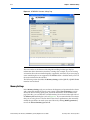
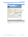
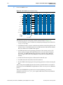
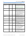
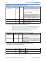
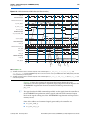
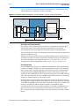
The ALTMEMPHY Parameter Settings page in the ALTMEMPHY MegaWizard
interface (Figure 2–1) allows you to parameterize the following settings:
1
f
© January 2010
■
Memory Settings
■
PHY Settings
■
Controller Interface Settings
The options for PHY Settings tab are editable if they apply to the Altera device that
you have chosen for your interface. Otherwise, the options are disabled. The options
for Controller Interface Settings tab are disabled when you are creating an
ALTMEMPHY (nonAFI) megafunction for QDR II+/QDR II SRAM interface.
For more information about the PHY Settings and the Controller Interface Settings,
refer to the Parameter Settings chapter in Volume 3: Implementing Altera Memory Interface
IP of the External Memory Interface Handbook
Altera Corporation
External Memory PHY Interface (ALTMEMPHY) (nonAFI) Megafunction User Guide
2–2
Chapter 2: Parameter Settings
Figure 2–1. ALTMEMPHY Parameter Settings Page
The text window at the bottom of the MegaWizard Plug-In Manager displays
information about the memory interface, warnings (for example, if you are creating
an interface above the maximum frequency supported), and errors if you are trying to
create something that is not supported. The Finish button is disabled until you fix all
the errors indicated in this window.
The following section describes the Memory Settings tab for QDR II+/QDR II SRAM
interface in more detail.
Memory Settings
In the Memory Settings tab, you can choose the frequency of operation for the device
and a particular memory device for your system. Under General Settings, you can
choose the device family, speed grade, and clock information. In the middle of the
page (left-side), you can filter the available memory device listed on the right side of
the Memory Presets dialog box, refer to Figure 2–1. If you cannot find the exact device
that you are using, choose a device that has the closest specifications, then manually
modify the parameters to match your actual device by clicking Modify parameters,
next to the Selected memory preset field.
External Memory PHY Interface (ALTMEMPHY) (nonAFI) Megafunction User Guide
© January 2010 Altera Corporation
Chapter 2: Parameter Settings
2–3
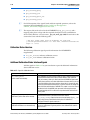
Table 2–1 describes the General Settings available on the Memory Settings page of
the ALTMEMPHY MegaWizard interface.
Table 2–1. General Settings
Parameter Name
Description
Device family
Targets device family. The device family selected here must match the device family selected on
MegaWizard page 2a.
Speed grade
Selects a particular speed grade of the device (for example, 2, 3, or 4 for the Stratix III device
family).
PLL reference clock
frequency
Determines the clock frequency of the external input clock to the PLL. Ensure that you use three
decimal points if the frequency is not a round number (for example, 166.667 MHz or 100 MHz) to
avoid a functional simulation or a PLL locking issue.
Memory clock
frequency
Determines the memory interface clock frequency. If you are operating a memory device below its
maximum achievable frequency, ensure that you enter the actual frequency of operation rather than
the maximum frequency achievable by the memory device. Also, ensure that you use three decimal
points if the frequency is not a round number (for example, 333.333 MHz or 400 MHz) to avoid a
functional simulation or a PLL locking issue.
Controller data rate
Selects the data rate for the memory controller. Sets the frequency of the controller to equal to
either the memory interface frequency (full-rate) or half of the memory interface frequency
(half-rate).
Local interface clock
frequency
This field’s value depends on the memory clock frequency and controller data rate, and whether or
not you turn on the Enable Half Rate Bridge option.
Local interface width
This field’s value depends on the memory clock frequency and controller data rate, and whether or
not you turn on the Enable Half Rate Bridge option.
Table 2–2 describes the options available to filter the Memory Presets that are
displayed. This section is where you indicate that you are creating a datapath for
QDR II+/QDR II SRAM.
Table 2–2. Memory Presets List
Parameter Name
Description
Memory type
You can filter the type of memory to display. For the ALTMEMPHY megafunction with nonAFI, select
QDR II+ SRAM and QDR II SRAM.
Memory vendor
You can filter the memory types by vendor. JEDEC is also one of the options, allowing you to
choose the JEDEC specifications. If your chosen vendor is not listed, you can choose Other for QDR
II+/QDR II SRAM interfaces. Then, pick a device that has similar specifications to your chosen
device and check the values of each parameter. Make sure you change the each parameter value to
match your device specifications.
Memory format
You can filter the type of memory by format (for example, components or DIMM packages). This
option is only available for DDR3, DDR2, and DDR SDRAM interfaces.
Maximum frequency
You can filter the type of memory by the maximum operating frequency.
© January 2010
Altera Corporation
External Memory PHY Interface (ALTMEMPHY) (nonAFI) Megafunction User Guide
2–4
Chapter 2: Parameter Settings
Use the Preset Editor to Create a Custom Memory Preset
Pick a device in the Memory Presets list that is closest or the same as the actual
memory device that you are using. Then, click the Modify Parameters button to
parameterize the following settings in the Preset Editor dialog box:
1
■
Memory attributes—These are the settings that determine your system's number of
DQ, DQS, address, and memory clock pins.
■
Memory initialization options—These settings are stored in the memory mode
registers as part of the initialization process.
■
Memory timing parameters—These are the parameters that create and
time-constraint the PHY.
Even though the device you are using is listed in Memory Presets, ensure that the
settings in the Preset Editor dialog box are accurate as some parameters may have
been updated in the memory device datasheets.
You can change the parameters with a white background to reflect your system. You
can also change the parameters with a gray background so the device parameters
match the device you are using. These parameters in gray background are
characteristics of the chosen memory device and changing them creates a new custom
memory preset. If you click Save As (at the bottom left of the page) and save the new
settings in the <quartus_install_dir>\quartus\common\ip\altera\altmemphy\lib\
directory, you can use this new memory preset in other Quartus II projects created in
the same version of the software.
When you click Save, the new memory preset appears at the bottom of the Memory
Presets list in the Memory Settings tab.
1
If you save the new settings in a directory other than the default directory, click Load
Preset in the Memory Settings tab to load the settings into the Memory Presets list.
External Memory PHY Interface (ALTMEMPHY) (nonAFI) Megafunction User Guide
© January 2010 Altera Corporation
Chapter 2: Parameter Settings
2–5
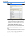
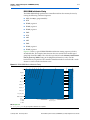
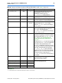
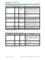
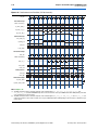
QDR II+/QDR II SRAM Preset Editor Page
Figure 2–2 shows the Preset Editor page for the ALTMEMPHY variation for
QDR II+/QDR II SRAM interfaces.
Figure 2–2. Preset Editor for QDR II+/QDR II SRAM Interfaces
Table 2–3 through Table 2–5 describe the QDR II+/QDR II SRAM parameters
available for memory attributes, initialization options, and timing parameters.
The QDR II+ SRAM devices have the same parameters as QDR II SRAM devices, but
their value ranges can differ. Confirm that the value you have chosen is valid in the
ALTMEMPHY MegaWizard interface.
© January 2010
Altera Corporation
External Memory PHY Interface (ALTMEMPHY) (nonAFI) Megafunction User Guide
2–6
Chapter 2: Parameter Settings
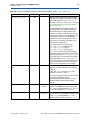
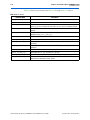
Table 2–3. QDR II+/QDR II SRAM Attribute Settings
Parameter Name
Range (1)
Units
Description
De-rate ×18 timing
for emulation ×36
mode
Enabled or Disabled
—
Allows the ALTMEMPHY megafunction to derate the timing
calculation when creating ×36 QDR II+/QDR II SRAM
interfaces by using two ×18 DQS/DQ groups. For more
information on ×36 emulation, refer to “Creating an Emulated
x36 QDR II+/QDR II SRAM ALTMEMPHY Variation” on
page 2–7.
Output clock pairs
from FPGA
1–16
pairs
Selects the number of differential clock pairs driven from the
FPGA to the memory. More clock pairs reduce the loading of
each output when interfacing with multiple memory devices.
Memory clock pins use the signal splitter feature in Stratix III
and Stratix IV devices for differential signaling.
Memory depth
expansion
1–2
chips
Picks the number of chip selects of memory supported. This
option is for memory depth expansion.
Memory interface
D/Q data bits
8–288
bits
Defines the width of external memory read and write data bus.
Multiply the number of devices with the number of DQ pins
per device when you create width-expanded memory
interfaces. Even though the GUI allows you to choose 288-bit
DQ width, the interface data width is limited by the number of
pins on the device. For best performance, have the whole
interface on one side of the device.
Memory vendor
Others
—
Displays the name of the memory vendor for all supported
memory standards.The ALTMEMPHY megafunction only has
generic QDR II+/QDR II SRAM data sheet information listed
under vendor as Other.
See the memory device
data sheet
MHz
Defines the maximum frequency supported by the memory.
Drive
BWS_N/NWS_N
from FPGA
Yes or No
—
Enables the use of the write select pins for write operations
when set to Yes.
DQ bits per chip
8, 9, 18, 36
bits
Defines the width of D and Q data bus on each QDRII SRAM
chip.
15–25
bits
Sets the number of address bits.
QDR II+ SRAM: 1.5 V
HSTL Class I;
QDR II SRAM: 1.8 V HSTL
Class I or 1.5 V HSTL
Class I
—
Selects the I/O standard to be applied to the memory interface
pins.
Maximum memory
frequency
Address width
I/O standard
Note to Table 2–3:
(1) The range values depend on the actual memory device used.
External Memory PHY Interface (ALTMEMPHY) (nonAFI) Megafunction User Guide
© January 2010 Altera Corporation
Chapter 2: Parameter Settings
2–7
Table 2–4. QDR II+/QDR II SRAM Initialization Options
Parameter Name
Memory burst
length
Memory latency
setting
Range
Units
Description
4
beats
Sets the memory burst length for the interface. As the
QDR II+/QDR II SRAM ALTMEMPHY megafunction only
supports half-rate designs, only a memory burst length of four
is supported, which equates to a local burst length of one.
1.5 (QDR II
SRAM) or 2.5
(QDR II+ SRAM)
Cycles
Sets the memory latency. Altera devices only support latency of
2.5 for QDR II+ SRAM and 1.5 for QDR II SRAM. QDR II+
SRAM with latency of 2.0 is not supported with Altera devices,
even though the ALTMEMPHY MegaWizard interface shows
this as an option.
Table 2–5. QDR II+/QDR II SRAM Timing Parameter Settings
Parameter Name
Range
Units
Description
tSA
200–500
ps
Address setup time to K clock rise.
tSC
200–500
ps
Control setup time to K clock rise.
tHA
200–500
ps
Address hold time to K clock rise.
tHC
200–500
ps
Control hold time after K clock rise.
tSD
200–500
ps
D setup time to K clock rise.
tHD
200–500
ps
D hold time to K clock rise.
tCQHQV
200–500
ps
Echo clock high to data valid.
tCQHQX
200–500
ps
Echo clock high to data invalid.
tCQHCQnH (1)
0–2,000
ps
Echo clock high to inverted echo clock high.
tCQH (1)
0–2,000
ps
Echo clock high.
Note to Table 2–5:
(1) This parameter is available for QDR II+ SRAM interfaces only.
Creating an Emulated x36 QDR II+/QDR II SRAM ALTMEMPHY Variation
From software implementation point of view, creating a ×36 emulated QDR II+/QDR
II SRAM interface is exactly the same as implementing an interface with two ×18
QDR II+/QDR II SRAM devices. In the Memory Settings page of the ALTMEMPHY
MegaWizard interface, select a ×18 QDR II+/QDR II SRAM with the same timing
specifications as ×36 QDR II+/QDR II SRAM device (see Figure 2–3).
For more information about ×36 emulation for QDR II+/QDR II SRAM interfaces,
refer to the Exceptions for ×36 Emulated QDR II and QDR II+ SRAM Interfaces in Arria II
GX, Stratix III and Stratix IV Devices section in Volume 2: Device, Pin, and Board Layout
Guidelines of the External Memory Interface Handbook.
© January 2010
Altera Corporation
External Memory PHY Interface (ALTMEMPHY) (nonAFI) Megafunction User Guide
2–8
Chapter 2: Parameter Settings
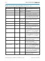
Figure 2–3. Select a ×18 Device
Emulated Device
Actual Device
To indicate that you are interfacing with 36-bit read and 36-bit write data follow these
steps:
1. On the Memory Settings page click Modify Parameters, to open the Preset Editor,
see Figure 2–4.
External Memory PHY Interface (ALTMEMPHY) (nonAFI) Megafunction User Guide
© January 2010 Altera Corporation
Chapter 2: Parameter Settings
2–9
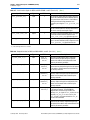
Figure 2–4. Preset Editor
2. For Derate ×18 timing for ×36 emulation mode, select Enabled. This setting tells
the report_timing.tcl script to use the derating factor for ×36 emulation. If you
have modified the board such that the slew rate of the ×36 emulated (doubleloaded) CQ/CQn signal is comparable to a non-emulated (single-loaded)
CQ/CQn signal, you can leave this option as Disabled, as there is no slew rate
degradation in your design.
3. For Output clock pairs from FPGA select 1. Only one mem_clk and mem_clk_n
pair connect to the QDR II+/QDR II SRAM device's K and Kn ports..
4. Memory interface D/Q data bits select 36, which is the data bus width for ×36
QDR II+/QDR II SRAM interfaces.
After generation, for devices with F780 and F1152 packages that do not have ×18 DQ
groups necessary to fit the write data bus, follow these steps to modify the
<variation_name>_pin_assignments.tcl file to change the assignments to use ×9 DQ
groups:
1. Remove the memory interface data pin group assignment of 18 for write data bus
and DM pins in the Assignment Editor.
2. Find the following assignments in the <variation_name>_pin_assignments.tcl.
set_instance_assignment -name MEMORY_INTERFACE_DATA_PIN_GROUP 18 -to
${d_pin_name}\[0..17\] -from ${d_pin_name}\[0\]
© January 2010
Altera Corporation
External Memory PHY Interface (ALTMEMPHY) (nonAFI) Megafunction User Guide
2–10
Chapter 2: Parameter Settings
set_instance_assignment -name MEMORY_INTERFACE_DATA_PIN_GROUP 18 -to
${dm_pin_name}\[0..1\] -from ${d_pin_name}\[0\]
set_instance_assignment -name MEMORY_INTERFACE_DATA_PIN_GROUP 18 -to
${d_pin_name}\[18..35\] -from ${d_pin_name}\[18\]
set_instance_assignment -name MEMORY_INTERFACE_DATA_PIN_GROUP 18 -to
${dm_pin_name}\[2..3\] -from ${d_pin_name}\[18\]
3. Replace with the following assignment:
set_instance_assignment -name MEMORY_INTERFACE_DATA_PIN_GROUP 9 -from
${d_pin_name}[0] -to ${d_pin_name}[0..8]
set_instance_assignment -name MEMORY_INTERFACE_DATA_PIN_GROUP 9 -from
${d_pin_name}[0] -to ${dm_pin_name}[0]
set_instance_assignment -name MEMORY_INTERFACE_DATA_PIN_GROUP 9 -from
${d_pin_name}[18] -to ${d_pin_name}[18..26]
set_instance_assignment -name MEMORY_INTERFACE_DATA_PIN_GROUP 9 -from
${d_pin_name}[18] -to ${dm_pin_name}[2]
set_instance_assignment -name MEMORY_INTERFACE_DATA_PIN_GROUP 9 -from
${d_pin_name}[9] -to ${d_pin_name}[9..17]
set_instance_assignment -name MEMORY_INTERFACE_DATA_PIN_GROUP 9 -from
${d_pin_name}[9] -to ${dm_pin_name}[1]
set_instance_assignment -name MEMORY_INTERFACE_DATA_PIN_GROUP 9 -from
${d_pin_name}[27] -to ${d_pin_name}[27..35]
set_instance_assignment -name MEMORY_INTERFACE_DATA_PIN_GROUP 9 -from
${d_pin_name}[27] -to ${dm_pin_name}[3]
4. Save the <variation_name>_pin_assignments.tcl file.
The rest of the RTL implementation is similar to a regular QDR II+/QDR II SRAM
interface.
External Memory PHY Interface (ALTMEMPHY) (nonAFI) Megafunction User Guide
© January 2010 Altera Corporation
3. Functional Description—ALTMEMPHY
(nonAFI)
This chapter describes the QDR II+/QDR II SRAM calibration process, the typical
PHY-to-Controller interfaces that are connected to the ALTMEMPHY variation and
the signal name prefixes each module uses for nonAFI variations.
1
Altera recommends that you use the AFI for new designs; only use the nonAFI for
existing designs.
QDR II+/QDR II SRAM Calibration Process
1
This section describes the calibration process for QDR II+/QDR II SRAM interfaces
only. For information about the calibration process for DDR2 and DDR SDRAM, refer
to the Calibration section in the DDR and DDR2 SDRAM High-Performance Controllers
and ALTMEMPHY IP User Guide.
The calibration process of a QDR II+/QDR II SRAM device is considerably simpler
than that of a calibration process for a DDR2/DDR SDRAM device. The calibration
process involves selecting the right phase of the resynchronization clock to capture
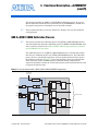
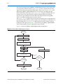
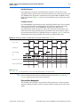
the read data at half rate. Figure 3–1 shows the generation of the resynchronization
clock which then clocks the HDR registers in the IOE. During calibration, the
sequencer determines whether to use the half-rate clock or the inverted half-rate clock
to capture the half-rate data.
Figure 3–1. Resynchronization Clock in QDR II+/QDR II SRAM ALTMEMPHY Megafunction
Input from
Sequencer
Shift Register
CQn
CQn
D
D
Q
D
Q
Q
D
Q
Half-Rate Data
shifted
D
© January 2010
Q
1/2
shifted
DQ
D
Altera Corporation
D
Q
D
Q
D
Q
Q
External Memory PHY Interface (ALTMEMPHY) (nonAFI) Megafunction User Guide
3–2
Chapter 3: Functional Description—ALTMEMPHY (nonAFI)
QDR II+/QDR II SRAM Calibration Process
The clock CQ coming from the QDR II+/QDR II SRAM is delayed and is divided by
two to generate a half-rate clock (resync_clk_1x). Data is captured on the rising
edges of the shifted CQ and shifted CQn signals. There is one resync_clk_1x per
DQS group. QDR II+/QDR II SRAM devices can only have one DQS group per
device, which means that there is one resync_clk_1x signal associated with each
memory device. This signal clocks the registers doing the full-rate to half-rate
conversion. It also clocks the front side of the read datapath clock-crossing FIFO.
There is one FIFO per DQS group (or memory device).
The resync_clk_1x signal can be inverted or not inverted. You can transfer data in
the correct byte order with one of these options. The main objective of calibration is to
find out whether the resync_clk_1x signal requires inversion, which is done by
loading the shift register, see Figure 3–1 (at most twice per QDR II+/QDR II SRAM
device). Each memory device is calibrated one after the other.
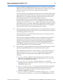
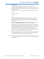
Figure 3–2 shows the QDR II+/QDR II SRAM calibration flowchart.
Figure 3–2. QDR II+/QDR II SRAM Calibration Flowchart
Calibration start
Write 0's pattern to address 3
Write 1's pattern to address 5
Setup resync_clk_1x phase associated with
DQS group being calibrated
Read 0's pattern
Read 1's pattern
Start latency counter and search for
0's followed by 1's pattern
If pattern found
No
Invert resync_clk_1x phase
No
Latency counter
timeout
Timed out for both
phases of
resync_clk_1x
All DQS groups
calibrated?
Yes
Yes
Align all DQS groups to worst case latency
Calibration
successful
External Memory PHY Interface (ALTMEMPHY) (nonAFI) Megafunction User Guide
Calibration
unsuccessful
© January 2010 Altera Corporation
Chapter 3: Functional Description—ALTMEMPHY (nonAFI)
QDR II+/QDR II SRAM Calibration Process
3–3
During the QDR II+/QDR II SRAM calibration, the sequencer first writes all 0s to
address space 3 in the external memory, followed by all 1s to address space 5. It then
loads the scan chain for the first time, to program the first setting for
resync_clk_1x.
The sequencer then starts reading 0s from address space 3 several times, followed by a
single read from address space 5 and starts the latency counter. If a pattern of all 0s
followed by all 1s is read before the latency counter reaches its time-out value (31
clock cycles), the latency value for that memory device is stored.
If all 0s followed by all 1s is not found when reading back from memory and the
latency count has reached the time-out value, the sequencer loads the scan chains a
second time to invert the resync_clk_1x signal. The sequencer then starts reading
from address space 3 several times, followed by a single read from address space 5 as
before and starts the latency counter again. If all 0s followed by all 1s are read back
from memory, the latency value for that memory device is stored.
1
The training pattern must be read back correctly on this second iteration (if it was not
already read correctly on the first iteration). If it is not read back correctly, it indicates
an underlying problem in the system.
The previous process is repeated until all memory devices are tested and a latency
value obtained for each device.
The latency values found for the different devices are compared with each other. If
necessary, they are aligned to the worst case latency (or to the user-requested
deterministic latency value if this option is used), which done by adjusting address
pointers in order to add latency to some of the read datapath RAMs inside the
ALTMEMPHY megafunction until the latency associated with all of the memory
devices is aligned to the worst case latency measured.
1
You cannot have a latency difference of more than two PHY clock cycles between all
the QDR II+/QDR II SRAM devices in non-deterministic latency mode.
When calibration has finished, the sequencer hands over control to the driver/user
logic, and generates the p_rdata_out_valid flag to indicate when read data is
valid. The sequencer also outputs the following signals upon completion of
calibration:
© January 2010
■
p_ready—Indicates completion of the calibration process (but does not mean
calibration was successful). This signal is renamed as the ctl_usr_mode_rdy
signal at the ALTMEMPHY top-level file.
■
p_calibration_successful—Indicates calibration was successfully
completed. This port is renamed resynchronisation_successful port at the
ALTMEMPHY top-level file.
■
p_user_defined_latency_ok—Indicates that the read latency requested by
the user was achievable, when using deterministic latency. This port is not
instantiated at the top-level of the file. Currently this signal exists at the
sequencer_wrapper file level only.
■
p_detectedlatency—Specifies the read latency achieved in phy_clk clock
cycles. This port is renamed ctl_rlat port at the ALTMEMPHY top-level file.
Altera Corporation
External Memory PHY Interface (ALTMEMPHY) (nonAFI) Megafunction User Guide
3–4
Chapter 3: Functional Description—ALTMEMPHY (nonAFI)
PHY-to-Controller Interfaces
VT tracking is not required because the read strobe from the QDR II+/QDR II SRAM
memory is continuous. So all registers in the I/O to the read RAM path are clocked
using a clock that is derived from the QDR II+/QDR II SRAM read clock.
1
For more information about the QDR II+/QDR II SRAM signals, refer to “QDR
II+/QDR II SRAM Signals” on page 3–20.
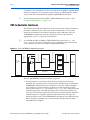
PHY-to-Controller Interfaces
The nonAFI’s autocalibration logic relies on the services of the memory controller to
perform its calibration writes, reads, and memory initialization, so it must have
control of the controller's local interface during the initial calibration stage. The
ALTMEMPHY megafunction has four interfaces that all must be connected
appropriately. Figure 3–3 shows the four interfaces.
1
As an SRAM, the PHY for QDR II+/QDR II SRAM lacks most of the ctl_ and
local_ ports as you can use a driver that acts as a controller to generate read and
write commands and data in the QDR II+/QDR II SRAM PHY.
Addr &
Cmd Path
Write path
Ports named mem_*
Memory
Controller
Ports named ctl_mem_*
Ports named ctl_*
User logic
(or example
driver)
Ports named local_*
Figure 3–3. The Four ALTMEMPHY Megafunction Interfaces
External
Memory
Read path
Auto-calibration
ALTMEMPHY
Clock & reset
management
The four ALTMEMPHY interfaces, from left to right, are:
1. The local interface is the interface between the user logic and the memory
controller. The signals between user logic and the controller traverse through the
ALTMEMPHY megafunction. This can either be an Avalon® Memory-Mapped
slave interface or a Native interface. All the ports on this interface have their
names prefixed with local_; for example, local_init_done. During the initial
calibration period, the auto-calibration logic takes control of this interface and
issues the write and read requests that the memory controller requires. When the
calibration process is complete, control is handed back to the user logic and
normal operation occurs. The ALTMEMPHY megafunction auto-calibration logic
does not require any further access to the memory controller when the initial
autocalibration is complete.
External Memory PHY Interface (ALTMEMPHY) (nonAFI) Megafunction User Guide
© January 2010 Altera Corporation
Chapter 3: Functional Description—ALTMEMPHY (nonAFI)
Initialization Timing
3–5
2. The ALTMEMPHY-controller local interface is the interface between the
ALTMEMPHY megafunction and the controller local interface. All the port names
on this interface are prefixed with ctl_; for example, ctl_init_done. This
interface connects the ALTMEMPHY megafunction to the controller’s local
interface and is of the same type as the local interface, either an Avalon-MM
interface or a native interface. When the calibration process is complete, this
connection becomes a straight-through connection and you have complete control
of the memory controller.
3. The ALTMEMPHY-controller command interface is the interface between the
controller and ALTMEMPHY. All the ports on this interface are prefixed with
ctl_mem_; for example, ctl_mem_rdata. They are clocked by the phy_clk.
This interface contains the memory control and address signals from the controller
to the memory. The controller also sends write data to, and receives read data
from, the external memory through this interface. All the signals on this interface
are clocked at the phy_clk rate. The ALTMEMPHY megafunction converts
between this clock and the memory interface clock.
4. The fourth interface is between the ALTMEMPHY megafunction and the external
memory devices and consists of the memory address, command, and data pins.
These must be connected directly to the external pins of your Altera FPGA.
Initialization Timing
DDR SDRAM initialization timing is different to DDR2 SDRAM initialization timing.
DDR SDRAM Initialization Timing
f
For DDR2 SDRAM initialization timing, see “DDR2 SDRAM Initialization Timing” on
page 3–7.
The DDR SDRAM high-performance controller initializes the SDRAM devices by
issuing the following memory command sequence:
■
NOP (for 200 µs, programmable)
■
PCH
■
Extended LMR (ELMR)
■
LMR
■
NOP (for 200 clock cycles, fixed)
■
PCH
■
ARF
■
ARF
■
LMR
Figure 3–4 on page 3–6 shows a typical initialization timing sequence. The length of
time between the reset and the first PCH command should be 200 µs. The value that
you specify for the Memory initialization time at power up (tINIt) setting in the
MegaWizard interface is only used for hardware that you generate. The controller
simulation model is created with a much shorter tINIT time to make simulation easier.
© January 2010
Altera Corporation
External Memory PHY Interface (ALTMEMPHY) (nonAFI) Megafunction User Guide
3–6
Chapter 3: Functional Description—ALTMEMPHY (nonAFI)
Initialization Timing
1
Do not set tINIT to zero.
Figure 3–4. DDR SDRAM Device Initialization Timing
[1]
[2]
[3]
[4]
[5]
[5]
[6]
clk
ddr_cke
0
ddr_a
0
ddr_ba
ddr_cs_n
0
1
0
0
0
0
0
0
0
0
P
L
L
P
A
A
L
ddr_ras_n
ddr_cas_n
ddr_we_n
local_init_done
DDR Command
Key:
P = PCH
L = LMR
A = ARF
200 clock cycles
The following sequence corresponds with the numbered items in Figure 3–4.
1. A PCH command is sent to all banks by setting the precharge pin, the address bit
a[10], or a[8] high.
2. An ELMR command is issued to enable the internal delay-locked loop (DLL) in the
memory devices. An ELMR command is an LMR command with the bank address
bits set to address the extended mode register.
3. An LMR command sets the operating parameters of the memory such as CAS
latency and burst length. This LMR command also resets the internal memory
device DLL. The DDR SDRAM high-performance controller allows 200 clock
cycles to elapse after a DLL reset and before it issues the next command to the
memory.
4. A further PCH command places all the banks in their idle state.
5. Two ARF commands must follow the PCH command.
6. The final LMR command programs the operating parameters without resetting the
DLL.
After issuing the final LMR command, the memory controller hands over control of
the memory to the ALTMEMPHY megafunction to allow it to carry out its calibration
process.
When the ALTMEMPHY megafunction has finished calibrating, the memory
controller asserts the local_init_done signal, which shows that it has initialized
the memory devices.
External Memory PHY Interface (ALTMEMPHY) (nonAFI) Megafunction User Guide
© January 2010 Altera Corporation
Chapter 3: Functional Description—ALTMEMPHY (nonAFI)
Initialization Timing
3–7
DDR2 SDRAM Initialization Timing
The DDR2 SDRAM high-performance controller initializes the memory devices by
issuing the following command sequence:
■
NOP (for 200 µs, programmable)
■
PCH
■
ELMR, register 2
■
ELMR, register 3
■
ELMR, register 1
■
LMR
■
PCH
■
ARF
■
ARF
■
LMR
■
ELMR, register 1
■
ELMR, register 1
Figure 3–5 shows a typical DDR2 SDRAM initialization timing sequence, which is
described below. The length of time between the reset and the clock enable signal
going high should be 200 µs. The value that you choose for the Memory initialization
time at power up (tINIt) setting in the MegaWizard interface is only used for
hardware that you generate. The controller simulation model is created with a much
shorter tINIT time to make simulation easier.
Figure 3–5. DDR2 SDRAM Device Initialization Timing
[1]
[2]
[3] [3]
[4]
[5]
[6]
[7]
[7]
[8]
[9]
clk
ddr_cke
ddr_a
2 0 3 0 1 0
ddr_ba
ddr_cs_n
0
0
0
0
0
0
0
0
P
L
L
L
L
P
A
1 0 1 1
ddr_ras_n
ddr_cas_n
ddr_we_n
local_init_done
DDR Command
A
Key:
P = PCH
L = LMR
A = ARF
L
N
L
L
200 clock cycles
Note to Figure 3–5:
(1) local_init_done only goes high when calibration has completed.
© January 2010
Altera Corporation
External Memory PHY Interface (ALTMEMPHY) (nonAFI) Megafunction User Guide
3–8
Chapter 3: Functional Description—ALTMEMPHY (nonAFI)
Initialization Timing
The following sequence corresponds with the numbered items in Figure 3–5 on
page 3–7.
1. The clock enable signal (CKE) is asserted 200 µs after coming out of reset.
2. The controller then waits 400 ns and then issues the first PCH command by setting
the precharge pin, the address bit a[10] or a[8] high. The 400 ns is calculated by
taking the number of clock cycles calculated by the wizard for the 200 µs delay and
dividing this by 500. If a small initialization time is selected for simulation
purposes, this delay is always at least 1 clock cycle.
3. Two ELMR commands are issued to load extend mode registers 2 and 3 with
zeros.
4. An ELMR command is issued to extend mode register 1 to enable the internal DLL
in the memory devices.
5. An LMR command is issued to set the operating parameters of the memory such
as CAS latency and burst length. This LMR command is also used to reset the
internal memory device DLL.
6. A further PCH command places all the banks in their idle state.
7. Two ARF commands must follow the PCH command.
8. A final LMR command is issued to program the operating parameters without
resetting the DLL.
9. 200 clock cycles after step 5, two ELMR commands are issued to set the memory
device off-chip driver (OCD) impedance to the default setting.
After issuing the final ELMR command, the memory controller hands over control of
the memory to the ALTMEMPHY megafunction to allow it to carry out its calibration
process.
When ALTMEMPHY megafunction has finished calibrating, the memory controller
asserts the local_init_done signal, which shows that it has initialized the memory
devices.
External Memory PHY Interface (ALTMEMPHY) (nonAFI) Megafunction User Guide
© January 2010 Altera Corporation
Chapter 3: Functional Description—ALTMEMPHY (nonAFI)
ALTMEMPHY Signals
3–9
ALTMEMPHY Signals
This section describes the ALMEMPHY megafunction signals for the following
interfaces:
■
DDR2 and DDR SDRAM signals
■
QDR II+ and QDR II SRAM signals
DDR2 and DDR SDRAM Signals
Table 3–1 through Table 3–10 show the signals for DDR2 and DDR SDRAM nonAFIs.
The signal lists include the following signal groups:
■
I/O interface to the external memory device
■
Clock and reset signals
■
PLL reconfiguration signals
■
External DLL signals
■
User-mode calibrated on-chip termination (OCT) control signals
■
Interface to the memory controller
■
Local interface signals
■
Datapath interface for the controller
■
ALTMEMPHY megafunction calibration status interface
■
Additional calibration signals from the sequencer
1
Ports with the prefix “mem_” connect the PHY with the memory device; ports with the
prefix “ctl_” connect the PHY with the controller. Ports with prefix “ctl_mem_”
indicate the datapath for the controller; ports with the prefix “local_” indicate the
signal to be connected with the example driver or user logic.
1
Signals with suffix _n are active low; signals without suffix _n are active high.
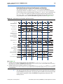
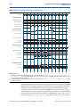
Table 3–1. I/O Interface for DDR2 and DDR SDRAM—nonAFI (Note 1) (Part 1 of 2)
Signal Name
Type
Width
Description
mem_addr
output
MEM_IF_ROWADDR_WIDTH
mem_ba
output
MEM_IF_BANKADDR_WIDTH
mem_cas_n
output
1
mem_cke
output
MEM_IF_CS_WIDTH
mem_clk
bidir
MEM_IF_CLK_PAIR_COUNT
The memory clock, positive edge clock. (2)
mem_clk_n
bidir
MEM_IF_CLK_PAIR_COUNT
The memory clock, negative edge clock. (2)
mem_cs_n
output
MEM_IF_CS_WIDTH
The memory chip select signal.
mem_dm
output
MEM_IF_DM_WIDTH
The optional memory data mask bus.
mem_dq
bidir
MEM_IF_DWIDTH
mem_dqs
bidir
MEM_IF_DWIDTH /
MEM_IF_DQ_PER_DQS
© January 2010
Altera Corporation
The memory row and column address bus.
The memory bank address bus.
The memory column address strobe.
The memory clock enable.
The memory bidirectional data bus.
The memory bidirectional data strobe bus.
External Memory PHY Interface (ALTMEMPHY) (nonAFI) Megafunction User Guide
3–10
Chapter 3: Functional Description—ALTMEMPHY (nonAFI)
ALTMEMPHY Signals
Table 3–1. I/O Interface for DDR2 and DDR SDRAM—nonAFI (Note 1) (Part 2 of 2)
Signal Name
Type
Width
Description
mem_dqsn
bidir
mem_odt
output
MEM_IF_CS_WIDTH
mem_ras_n
output
1
The memory row address strobe.
mem_reset_n
output
1
The memory-reset signal.
mem_we_n
output
1
The memory write-enable signal.
MEM_IF_DWIDTH /
MEM_IF_DQ_PER_DQS
The memory bidirectional data strobe bus. Not used in
Arria GX, HardCopy II, Stratix II, and Stratix II GX
designs.
The memory on-die termination control signal.
Notes to Table 3–1:
(1) Connected to I/O pads.
(2) Output is for memory device, and input path is fed back to ALTMEMPHY megafunction for VT tracking.
Table 3–2. Clock and Reset Signals for DDR2/DDR SDRAM—nonAFI (Note 1) (Part 1 of 2)
Signal Name
Type
Width
Description
global_reset_n (1)
input
1
The asynchronous reset input to the controller. All other
reset signals are derived from resynchronized versions of
this. This signal holds the complete ALTMEMPHY
megafunction, including the PLL, in reset while low.
soft_reset_n (1)
input
1
The asynchronous reset input to reset controller, for
SOPC Builder use, or to be controlled by other system
reset logic. This signal causes a complete reset of the
PHY, but not the PLL in the PHY. In Arria GX, Stratix II,
and Stratix II GX devices, this signal also resets the PLL
reconfiguration block on a falling-edge detection.
phy_clk
output
1
The ALTMEMPHY megafunction half-rate clock provided
to the user. All user inputs and outputs to the
ALTMEMPHY megafunction are synchronous to this clock
in half-rate designs. However, this clock is not used in
full-rate designs.
pll_ref_clk
input
1
The reference clock input to PLL.
reset_phy_clk_n (1)
output
1
Asynchronous reset, that is de-asserted synchronously
with respect to the associated phy_clock clock
domain. Use this to reset any additional user logic on that
clock domain.
reset_request_n (1)
output
1
Directly connected to the locked output of the PLL and is
intended for optional use either by automated tools such
as SOPC Builder or could be manually ANDed with any
other system-level signals and combined with any edge
detect logic as required and then fed back to the
global_reset_n input.
Reset request output that indicates when the PLL outputs
are not locked. Use this as a reset request input to any
system-level reset controller you may have. This signal is
always low while the PLL is locking (but not locked), and
so any reset logic using it is advised to detect a reset
request on a falling-edge rather than by level detection.
aux_half_rate_clk
output
1
A copy of the phy_clk_1x signal that you can use in
other parts of your design, same as phy_clk port.
External Memory PHY Interface (ALTMEMPHY) (nonAFI) Megafunction User Guide
© January 2010 Altera Corporation
Chapter 3: Functional Description—ALTMEMPHY (nonAFI)
ALTMEMPHY Signals
3–11
Table 3–2. Clock and Reset Signals for DDR2/DDR SDRAM—nonAFI (Note 1) (Part 2 of 2)
Signal Name
aux_full_rate_clk
Type
Width
output
1
Description
A copy of the mem_clk_2x signal that you can use in
other parts of your design.
Note to Table 3–2:
(1) Refer to Figure 4–3 for the reset mechanism in Arria GX, Cyclone III, Stratix II and Stratix II GX devices.
The ports in Table 3–3 exists for all DDR2/DDR SDRAM variations.
Table 3–3. PLL Reconfiguration Signals for DDR2 and DDR SDRAM—nonAFI
Signal Name
Type
Width
Description
pll_reconfig_
enable
input
1
Allows access to the PLL reconfiguration block. Hold this
signal low in normal operation. While the ALTMEMPHY is held
in reset (via the soft_reset_n signal), and the
reset_request_n signal is 1, it is safe to reconfigure the
PLL. To reconfigure the PLL, set this signal to 1 and use the
other pll_reconfig signals to access the PLL. When
finished reconfiguring, set this signal to 0, and then set the
soft_reset_n signal to 1 to bring the ALTMEMPHY out of
reset. For this signal to work, the
PLL_RECONFIG_PORTS_EN parameter must be set to
TRUE.
pll_reconfig_
write_param
input
1
For more information, refer to the Phase-Locked Loop
(ALTPLL_RECONFIG) User Guide.
pll_reconfig_read
_param
input
1
For more information, refer to the Phase-Locked Loop
(ALTPLL_RECONFIG) User Guide.
pll_reconfig
input
1
For more information, refer to the Phase-Locked Loop
(ALTPLL_RECONFIG) User Guide.
pll_reconfig_
counter_type
input
4
For more information, refer to the Phase-Locked Loop
(ALTPLL_RECONFIG) User Guide.
pll_reconfig_
counter_param
input
3
For more information, refer to the Phase-Locked Loop
(ALTPLL_RECONFIG) User Guide.
pll_reconfig_data
_in
input
9
For more information, refer to the Phase-Locked Loop
(ALTPLL_RECONFIG) User Guide.
pll_reconfig_soft
_reset_en_n
input
1
The asynchronous reset input to the PLL reconfiguration
block. This reset causes a PLL reconfiguration block reset and
holds the reset if the ALTMEMPHY megafunction in reset while
the signal is low. This port only exists in the DDR2/DDR
SDRAM variation for Arria GX, Stratix II, and Stratix II GX
devices.
pll_reconfig_busy
output
1
For more information, refer to the Phase-Locked Loop
(ALTPLL_RECONFIG) User Guide.
pll_reconfig_data
_out
output
9
For more information, refer to the Phase-Locked Loop
(ALTPLL_RECONFIG) User Guide.
pll_reconfig_clk
output
1
Synchronous clock to use for any logic accessing the PLL
reconfiguration interface.
pll_reconfig_
reset
output
1
Resynchronized reset to use for any logic accessing the PLL
reconfiguration interface.
© January 2010
Altera Corporation
External Memory PHY Interface (ALTMEMPHY) (nonAFI) Megafunction User Guide
3–12
Chapter 3: Functional Description—ALTMEMPHY (nonAFI)
ALTMEMPHY Signals
Table 3–4. External DLL Signals for DDR2 and DDR SDRAM—nonAFI
Signal Name
Type
Width
Description
dqs_delay_ctrl_
export
output
6
Allows sharing DLL in this ALTMEMPHY instance with another
ALTMEMPHY instance. Connect the
dqs_delay_ctrl_export port on the ALTMEMPHY
instance with a DLL to the dqs_delay_ctrl_import port
on the other ALTMEMPHY instance.
dqs_delay_ctrl_
import
input
6
Allows the use of DLL in another ALTMEMPHY instance in this
ALTMEMPHY instance. Connect the
dqs_delay_ctrl_export port on the ALTMEMPHY
instance with a DLL to the dqs_delay_ctrl_import port
on the other ALTMEMPHY instance.
dll_reference_
clk
output
1
Reference clock to feed to an externally instantiated DLL. This
clock is typically from one of the PHY PLL outputs.
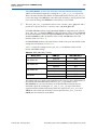
The ports listed in Table 3–5 only exist when you target Stratix III and Stratix IV
devices. You can leave them unconnected if you are not using user-mode calibrated
OCT. For more information about Stratix III and Stratix IV ports, refer to
ALTMEMPHY Signals section in chapter 5 of the DDR and DDR2 SDRAM
High-Performance Controllers and ALTMEMPHY IP User Guide.
Table 3–5. User-Mode Calibrated OCT Control Signals for DDR2/DDR SDRAM—nonAFI
(Note 1), (2)
Signal Name
Type
Width
Description
oct_ctl_rs_value
input
14
Specifies serial termination value. Connects to the
seriesterminationcontrol bus of the ALT_OCT
megafunction. This port exists when you target Stratix IV and
Stratix III devices only.
oct_ctl_rt_value
input
14
Specifies parallel termination value. Connects to the
parallelterminationcontrol bus of the ALT_OCT
megafunction. This port exists when you target Stratix IV and
Stratix III devices only.
Notes to Table 3–5:
(1) These ports are available if you want to use user-mode OCT calibration. Otherwise, they can be left unconnected.
(2) For more information on OCT, see the ALT_OCT Megafunction User Guide.
External Memory PHY Interface (ALTMEMPHY) (nonAFI) Megafunction User Guide
© January 2010 Altera Corporation
Chapter 3: Functional Description—ALTMEMPHY (nonAFI)
ALTMEMPHY Signals
3–13
Table 3–6. Interface to the Memory Controller for DDR2 and DDR SDRAM—nonAFI (Note 1) (Part 1 of 3)
Signal Name
ctl_add_1t_ac_lat
Type
Width
Description
input
1
When asserted, one extra address and command
clock cycle (1T) of latency is inserted in the address
and command path if the ADDR_CMD_ADD_1T
parameter is set to EXT_SELECT, see “Handshake
Mechanism Between Write Commands and Write
Data” on page 3–49.
For DDR SDRAM, the write latency is fixed at one
memory clock cycle, but for DDR2 SDRAM, this
value changes with the read CAS latency. As the
controller is running at half the rate of the memory
clock, a latency change of one controller clock cycle
is two memory clock cycles. The ALTMEMPHY
megafunction allows you to dynamically insert an
extra memory clock of delay in the address and
command path to compensate.
The insertion of delay is controlled by the
ADDR_CMD_ADD_1T parameter and the
ctl_add_1t_ac_lat signal. If
ADDR_CMD_ADD_1T is set to the string
EXT_SELECT, an extra cycle of latency can be
dynamically inserted on the address and command
outputs by asserting the ctl_add_1t_ac_lat
input, which allows run-time control of the address
and command latency. If ADDR_CMD_ADD_1T is
set to the string value TRUE, the extra clock cycle of
latency is always present. If it is set to the string
value FALSE, the extra latency is never added.
ctl_add_intermediate_
regs
Input
1
When asserted, an additional intermediate register or
registers is included in the address and command
path if the
ADDR_CMD_ADD_INTERMEDIATE_REGS
parameter is set to EXT_SELECT.
For Stratix II and Cyclone III devices only, to maintain
the clock cycle relationship between
address/command and the write data. You must
include the address/command phases where
required.
ctl_address
output
LOCAL_IF_
AWIDTH
output
ctl_be
© January 2010
Altera Corporation
LOCAL_IF_
DWIDTH/8
The address corresponding to a write or read
request. The ALTMEMPHY sequencer logic drives
ctl_address during calibration. ctl_address
has the same timing as local_address.
The output to the controller indicating the
byte-enable flags. The ALTMEMPHY sequencer logic
drives ctl_be during calibration. ctl_be is
mandatory and has the same timing as local_be.
External Memory PHY Interface (ALTMEMPHY) (nonAFI) Megafunction User Guide
3–14
Chapter 3: Functional Description—ALTMEMPHY (nonAFI)
ALTMEMPHY Signals
Table 3–6. Interface to the Memory Controller for DDR2 and DDR SDRAM—nonAFI (Note 1) (Part 2 of 3)
Signal Name
ctl_doing_rd
Type
Width
Description
input
1
The active-high signal from the controller specifying
that a read command has been issued to the external
RAM.
For more information, see “Handshake Mechanism
Between Read Commands and Read Data” on
page 3–47.
ctl_init_done
input
1
The memory controller drives this active-high signal
to specify that the controller has initialized the
memory and the calibration process should begin.
ctl_negedge_en
input
1
This signal is used if ADDR_CMD_NEGEDGE_EN is
set to EXT_SELECT. If true, the address and
command signals are output on the falling edge of
the address and command clock, ac_clk_2x. If
false, the address and command signals are output
on the rising edge of the address and command
clock. When set to EXT_SELECT, the
ctl_negedge_en top level input determines
whether the edge is used.
ctl_read_req
output
1
The active-high signal requesting a read command to
the address on the ctl_address bus.
ctl_ready
input
1
The controller-ready signal which indicates that the
currently asserted read or write request has been
accepted. The address of the request is sampled
when both the ready and request signals are high.
ctl_size
output
ctl_usr_mode_rdy
output
1
ctl_wdata
output
LOCAL_IF_
DWIDTH
ctl_wdata_req
input
1
LOCAL_
The output to the controller indicating the size
BURST_LEN_ (length) of the burst transfer, fixed at 1 for this
BITS
version.
The ALTMEMPHY sequencer logic drives this
active-high signal to specify the ALTMEMPHY has
finished its calibration and is ready to accept user
read or write requests.
The write data from the ALTMEMPHY to the
controller. The ALTMEMPHY sequencer logic drives
ctl_wdata during calibration. ctl_wdata has
the same timing as local_wdata.
The controller-request for write data; not required
when the controller has an Avalon-MM interface.
The memory controller that the ALTMEMPHY
sequencer uses during calibration drives
ctl_wdata_req. Same timing as
local_wdata_req.
ctl_write_req
output
1
External Memory PHY Interface (ALTMEMPHY) (nonAFI) Megafunction User Guide
The active-high signal specifying that a write
command should be issued to the address on the
ctl_address signal. The ALTMEMPHY
sequencer logic drives ctl_write_req during
calibration. Same timing as local_write_req.
© January 2010 Altera Corporation
Chapter 3: Functional Description—ALTMEMPHY (nonAFI)
ALTMEMPHY Signals
3–15
Table 3–6. Interface to the Memory Controller for DDR2 and DDR SDRAM—nonAFI (Note 1) (Part 3 of 3)
Signal Name
Type
Width
Description
ctl_refresh_ack
input
1
The active-high valid signal from the controller
acknowledging the refresh request. The
ALTMEMPHY sequencer logic uses
ctl_refresh_ack during calibration.
ctl_refresh_req
output
1
The output to the controller requesting a refresh.
Same timing as local_refresh_req.
ctl_burstbegin
output
1
The output to the controller indicating the start of a
burst. Only available for the Avalon-MM interface.
ctl_rdata
input
LOCAL_IF_
DWIDTH
The read data from the controller. The ALTMEMPHY
sequencer logic uses ctl_rdata during
calibration. ctl_rdata has the same timing as
local_rdata.
ctl_rdata_valid
input
1
The active-high valid signal for the controller read
data. Asserted coincident with the read data on
ctl_rdata. The controller drives
ctl_rdata_valid and has the same timing as
local_rdata_valid.
ctl_add_1t_odt_lat
input
1
When asserted, one extra address and command
clock cycle (1T) of latency is inserted in the address
and command ODT path if ODT_ADD_1T is set to
EXT_SELECT, see “Handshake Mechanism
Between Write Commands and Write Data” on
page 3–49.
The timing of the mem_odt signal can be controlled
in the same way as mem_addr, but is independent
of the address and command latency. If the
ODT_ADD_1T parameter is set to EXT_SELECT,
an extra cycle of latency can be dynamically inserted
on the ODT command outputs by asserting the
ctl_add_1t_odt_lat input, which allows
separate run-time control of the latency of the ODT
signal. If ODT_ADD_1T is set to TRUE, the extra
clock cycle of latency is always present. If
ODT_ADD_1T is set to FALSE, the extra latency is
never added.
ctl_rlat
output
READ_LAT_
WIDTH
Unused port that exists when you target Stratix IV
and Stratix III devices. The default
READ_LAT_WIDTH is set to 4.
ctl_self_rfsh_ack
input
1
ctl_powerdn_ack
input
1
Signal from the Altera high-performance controller
that is passed through the PHY.
ctl_autopch_req
output
1
ctl_powerdn_req
output
1
ctl_self_rfsh_req
output
1
Note to Table 3–6:
(1) Interface signals to the controller either through the sequencer or user interface.
© January 2010
Altera Corporation
External Memory PHY Interface (ALTMEMPHY) (nonAFI) Megafunction User Guide
3–16
Chapter 3: Functional Description—ALTMEMPHY (nonAFI)
ALTMEMPHY Signals
Table 3–7. Local Interface Signals for DDR2 and DDR SDRAM—nonAFI (Part 1 of 2)
Signal Name
(Note 1)
Type
Width
local_address
input
LOCAL_IF_
AWIDTH
The address corresponding to a write or read
request.
local_be
input
LOCAL_IF_
DWIDTH / 8
The input to ALTMEMPHY megafunction indicating
the byte-enable flags.
local_read_req
input
1
The active-high signal requesting a read command
to the address on the ctl_address bus.
local_ready
output
1
The controller-ready signal which indicates that the
currently asserted read or write request has been
accepted. The address of the request is sampled
when both the ready and request signals are high.
local_size
input
LOCAL_
BURST_LEN_
BITS
The controller signal to indicate the size (length) of
the burst transfer, fixed at 1 for this version.
local_wdata
input
LOCAL_IF_
DWIDTH
The write data from the user to the ALTMEMPHY
megafunction.
local_wdata_req
output
1
The controller request for write data; not required
when the controller has an Avalon-MM interface.
local_write_req
input
1
The active-high signal specifying that a write
command should be issued to the address on the
ctl_address signal.
local_refresh_req
input
1
The ALTMEMPHY megafunction receives refresh
requests from the local interface and passes them to
the controller via ctl_refresh_req when in
user mode (ctl_usr_mode output is high).
local_burstbegin
input
1
The ALTMEMPHY megafunction receives the
burstbegin signal from the local interface and
passes it to the controller via ctl_burstbegin
when in user mode (ctl_usr_mode output is
high).
local_rdata
output
LOCAL_IF_
DWIDTH
When ctl_usr_mode is high, this output passes
through the read data from the controller to the local
interface. Otherwise, it is tied low.
local_rdata_valid
output
1
When ctl_usr_mode is high, this output passes
through the read data valid signal
(ctl_rdata_valid) from the controller to the
local interface. Otherwise, it is driven low.
local_init_done
output
1
When ctl_usr_mode is high, this output passes
through the controller’s initialization done signal
(ctl_init_done) from the controller to the local
interface. Otherwise, it is driven low.
local_refresh_ack
output
1
When ctl_usr_mode is high, this output passes
through the controller’s refresh acknowledge signal
(ctl_refresh_ack) from the controller to the
local interface. Otherwise, it is driven low.
local_autopch_req
input
1
User control for auto precharge to request the
controller to issue an autoprecharge write or
autoprecharge read command.
External Memory PHY Interface (ALTMEMPHY) (nonAFI) Megafunction User Guide
Description
© January 2010 Altera Corporation
Chapter 3: Functional Description—ALTMEMPHY (nonAFI)
ALTMEMPHY Signals
3–17
Table 3–7. Local Interface Signals for DDR2 and DDR SDRAM—nonAFI (Part 2 of 2)
Signal Name
(Note 1)
Type
Width
Description
local_powerdn_req
input
1
User control to power down the memory device to
request the controller to place the memory devices
into a power-down state as soon as it can without
violating the relevant timing parameters and
responds by asserting the local_powerdn_ack
signal.
local_self_rfsh_req
input
1
User control of the self-refresh feature to request
that the controller place the memory devices into a
self-refresh state by asserting this signal.
local_self_rfsh_ack
output
1
Self-refresh request acknowledge signal. This signal
is asserted and deasserted in response to the
local_self_rfsh_req signal from the user.
local_powerdn_ack
output
1
Power-down request acknowledge signal. This
signal is asserted and deasserted in response to the
local_powerdn_req signal from the user.
Note to Table 3–7:
(1) Passed through PHY to the controller.
Table 3–8. Datapath Interface for DDR2 and DDR SDRAM—nonAFI (Part 1 of 3)
Signal Name
(Note 1)
Type
Width
ctl_mem_addr_h (1)
input
MEM_IF_
ROWADDR_
WIDTH
The row or column address that is sent to the
external memory. Output during the high halfperiod of the address and command clock and
driven by the memory controller.
ctl_mem_addr_l (1)
input
MEM_IF_
ROWADDR_
WIDTH
The row or column address that is sent to the
external memory. Output during the low half-period
of the address and command clock and driven by
the memory controller.
ctl_mem_ba_h (1)
input
MEM_IF_
BANKADDR_
WIDTH
The bank address that is sent to the external
memory. Output during the high half-period of the
address and command clock and driven by the
memory controller.
ctl_mem_ba_l (1)
input
MEM_IF_
BANKADDR_
WIDTH
The bank address that is sent to the external
memory. Output during the low half-period of the
address and command clock and driven by the
memory controller.
ctl_mem_be
input
LOCAL_IF_
DWIDTH/8
The optional byte-enable signals for the write data
to the external memory. The ALTMEMPHY
megafunction converts the byte enables into
memory mem_dm signals. If mem_dm pins are not
required (mem_dm_pins set to FALSE), the
mem_dm logic is not generated and the mem_dm
pins are not instantiated.
ctl_mem_cas_n_h (1)
input
1
The column-address strobe signal from the
controller to the memory. Output during the high
half-period of the address and command clock and
driven by the memory controller.
© January 2010
Altera Corporation
Description
External Memory PHY Interface (ALTMEMPHY) (nonAFI) Megafunction User Guide
3–18
Chapter 3: Functional Description—ALTMEMPHY (nonAFI)
ALTMEMPHY Signals
Table 3–8. Datapath Interface for DDR2 and DDR SDRAM—nonAFI (Part 2 of 3)
Signal Name
(Note 1)
Type
Width
Description
ctl_mem_cas_n_l (1)
input
1
The column-address strobe signal from the
controller to the memory. Output during the low
half-period of the address and command clock and
driven by the memory controller.
ctl_mem_cke_h (1)
input
MEM_IF_CS_
WIDTH
The clock-enable signal from the controller to the
memory. Output during the high half-period of the
address and command clock and driven by the
memory controller.
ctl_mem_cke_l (1)
input
MEM_IF_CS_
WIDTH
The clock-enable signal from the controller to the
memory. Output during the low half-period of the
address and command clock and driven by the
memory controller.
ctl_mem_cs_n_h (1)
input
MEM_IF_CS_
WIDTH
The chip-select signal from the controller to the
memory. For half-rate designs, always tie
ctl_mem_cs_n_h high, as even with 2T
addressing, the chip select is only driven for the
second clock cycle, to allow an extra clock cycle of
setup time for the other address and command
signals. Output during the high half-period of the
address and command clock and driven by the
memory controller
ctl_mem_cs_n_l (1)
input
MEM_IF_CS_
WIDTH
The chip-select signal from the controller to the
memory. Output during the low half-period of the
address and command clock and driven by the
memory controller.
ctl_mem_dqs_burst
input
1
Controls the DQS output enables of the DQS pins.
ctl_mem_odt_h (1)
input
MEM_IF_CS_
WIDTH
The on-die termination signal from the controller to
the memory.
ctl_mem_odt_l (1)
input
MEM_IF_CS_
WIDTH
The on-die termination signal from the controller to
the memory.
ctl_mem_ras_n_h (1)
input
1
The row-address strobe signal from the controller
to the memory. Output during the high half-period
of the address and command clock and driven by
the memory controller.
ctl_mem_ras_n_l (1)
input
1
The row-address strobe signal from the controller
to the memory. Output during the low half-period of
the address and command clock and driven by the
memory controller.
ctl_mem_rdata
output
LOCAL_IF_
DWIDTH
ctl_mem_rdata_valid
output
1
The ctl_mem_rdata signal is the captured,
resynchronized, and demultiplexed read data from
the ALTMEMPHY megafunction to the controller.
The ctl_mem_rdata_valid signal Indicates
when the ctl_mem_rdata is valid.
For more information, see “Handshake Mechanism
Between Read Commands and Read Data” on
page 3–47.
External Memory PHY Interface (ALTMEMPHY) (nonAFI) Megafunction User Guide
© January 2010 Altera Corporation
Chapter 3: Functional Description—ALTMEMPHY (nonAFI)
ALTMEMPHY Signals
3–19
Table 3–8. Datapath Interface for DDR2 and DDR SDRAM—nonAFI (Part 3 of 3)
Signal Name
(Note 1)
Type
Width
Description
ctl_mem_wdata
input
MEM_IF_
DWIDTH×
DWIDTH_
RATIO
The write data bus, which has valid data in the same
clock cycles that control_wdata_valid is
asserted, see “Handshake Mechanism Between
Read Commands and Read Data” on page 3–47.
ctl_mem_wdata_valid
input
1
Generates the mem_dq output enable. When
asserted, the ctl_mem_rdata_valid signal
indicates that the coincident read data on
ctl_mem_rdata is valid.
ctl_mem_we_n_h (1)
input
1
The write-enable signal from the controller to the
memory. Output during the high half-period of the
address and command clock and driven by the
memory controller.
ctl_mem_we_n_l (1)
input
1
The write-enable signal from the controller to the
memory. Output during the low half-period of the
address and command clock and driven by the
memory controller.
Note to Table 3–8:
(1) The “_h” and “_l” stand for high and low. They signify in which half of the clock cycle the data is output. The _h data is output when the
corresponding clock, for example ac_clk_2x, is high. The _l data is output when the ac_clk_2x clock is low. The signals with _h and
_l allow you to select between 1T and 2T addressing. For half-rate designs, 1T is where the address and command signals are driven for one
clock; 2T is where they are driven for 2 clocks. For full-rate designs, ensure the same signal drives both _h and _l signals and 2T addressing
is used. Also when high-performance controllers use ALTMEMPHY, 2T addressing is used.
Table 3–9. Calibration Status Interface for DDR2 and DDR SDRAM—nonAFI
Signal Name
Type
Width
resynchronisation_
successful
output
1
Active-high signal that is set to indicate that
calibration of the read data resynchronization clock
phase was completed and successful.
postamble_successful
output
1
Active-high signal that is set to indicate that read
postamble calibration was completed.
tracking_successful
output
1
Active-high signal that is set to indicate the
completion of mimic path VT variation tracking
operation.
tracking_adjustment_
up
output
1
Active-high signal that is pulsed to indicate that the
mimic path tracking has adjusted the
resynchronization clock phasing upwards.
tracking_adjustment_
down
output
1
Active-high signal that is pulsed to indicate that the
mimic path tracking has adjusted the
resynchronization clock phasing downwards.
© January 2010
Altera Corporation
Description
External Memory PHY Interface (ALTMEMPHY) (nonAFI) Megafunction User Guide
3–20
Chapter 3: Functional Description—ALTMEMPHY (nonAFI)
ALTMEMPHY Signals
Table 3–10 shows additional calibration status signal outputs from the sequencer. You
can either pull these signals out to the top level or observe them through the
SignalTap® II logic analyzer.
Table 3–10. Additional Calibration Status Signals—nonAFI
Signal
Description
The ALTMEMPHY resynchronization setup unit (RSU) sweeps the phase of a
resynchronization clock across 360° (full-rate designs) or 720° (half-rate designs) of
a memory clock cycle. Data reads from the DIMM are performed for each phase
position and a data valid window is located, which is the set of resynchronization
clock phase positions where data is successfully read. The final resynchronization
clock phase is set at the center of this range: the center of the data valid window
(CODVW). This output is set to the current calculated value for the CODVW and
represents how many phase steps were performed by the PLL to offset the
resynchronization clock from the memory clock.
rsu_codvw_phase
(Center of data valid window)
If the RSU can find one data valid window (and not more than one), the
resynchronization clock is positioned at the center and the rsu_read_latency
output is then set to the read latency (in phy_clk cycles) using that
resynchronization clock phase. If calibration is unsuccessful, this signal remains at 0.
rsu_read_latency
(Read latency at the center of the
window)
rsu_no_dvw_err
(Calibration failed due to no window
found)
If the RSU sweeps the resynchronization clock across every phase and does not see
any valid data at any phase position, calibration fails and this output is set to 1.
(Calibration failed due to more than
one valid window)
If the RSU sweeps the resynchronization clock across every phase and sees multiple
data valid windows, this indicates unexpected read data (random bit errors) or an
incorrectly configured PLL, which must be resolved. Calibration has failed and this
output is set to 1.
rsu_multiple_valid_
latencies_err
If the RSU sweeps the resynchronization clock across every phase and sees valid
data at more than two different latencies, calibration fails and this output is set to 1.
rsu_grt_one_dvw_err
(Calibration failed due to more than
two read latencies)
QDR II+/QDR II SRAM Signals
This section describes the ALMEMPHY megafunction signals for QDR II+/QDR II
SRAM.
Table 3–11 through Table 3–15 show the signals.
1
Signals with the prefix mem_ connect the PHY with the memory device; signals with
the prefix ctl_ connect the PHY with the controller.
Table 3–11. I/O Interface to QDR II+/QDR II SRAM (Note 1) (Part 1 of 2)
Signal Name
Type
Width
mem_addr
output
MEM_IF_ROWADDR_
WIDTH
Memory address bus.
mem_clk
output
MEM_IF_CLK_PAIR
_COUNT
Memory clock, positive edge clock (K).
mem_clk_n
output
MEM_IF_CLK_PAIR
_COUNT
Memory clock, positive edge clock (K#) 180° offset
from mem_clk.
External Memory PHY Interface (ALTMEMPHY) (nonAFI) Megafunction User Guide
Description
© January 2010 Altera Corporation
Chapter 3: Functional Description—ALTMEMPHY (nonAFI)
ALTMEMPHY Signals
3–21
Table 3–11. I/O Interface to QDR II+/QDR II SRAM (Note 1) (Part 2 of 2)
Signal Name
Type
Width
Description
mem_d
output
MEM_IF_DWIDTH
Memory data bus. D input to QDR II SRAM device.
mem_dm
output
MEM_IF_DM_WIDTH
Memory write select. BWS# input to QDR II SRAM
device.
mem_dq
input
MEM_IF_DWIDTH
mem_dqs
input
MEM_IF_DWIDTH /
MEM_IF_DQ_PER_
DQS
Memory read clock high bits (CQ).
mem_dqsn
input
MEM_IF_DWIDTH /
MEM_IF_DQ_PER_
DQS
Memory read clock low bits (CQn).
mem_doff_n
output
1
Memory DLL disable control.
mem_rps_n
output
MEM_IF_CS_WIDTH
Memory read enable signal.
mem_wps_n
output
MEM_IF_CS_WIDTH
Memory write enable signal.
Memory data bus. Q output from QDR II SRAM
device.
Note to Table 3–11:
(1) Connected to WYSIWYGS/pad atoms.
Table 3–12. Clock and Reset Signals for QDR II+/QDR II SRAM (Part 1 of 2)
Signal Name
Type
Width
Description
global_reset_n (1)
input
1
The asynchronous reset input to the controller. All other
reset signals are derived from resynchronized versions of
this. This signal holds the complete ALTMEMPHY
megafunction, including the PLL, in reset while low.
soft_reset_n (1)
input
1
The asynchronous reset input to reset controller, for
SOPC Builder use, or to be controlled by other system
reset logic. This signal causes a complete reset of the
PHY, but not the PLL in the PHY. In Arria GX, Stratix II,
and Stratix II GX devices, this signal also resets the PLL
reconfiguration block on a falling-edge detection.
phy_clk
output
1
The ALTMEMPHY megafunction half-rate clock provided
to the user. All user inputs and outputs to the
ALTMEMPHY megafunction are synchronous to this clock
in half-rate designs. However, this clock is not used in
full-rate designs.
pll_ref_clk
input
1
The reference clock input to PLL.
reset_phy_clk_n (1)
output
1
Asynchronous reset, that is de-asserted synchronously
with respect to the associated phy_clock clock
domain. Use this to reset any additional user logic on that
clock domain.
© January 2010
Altera Corporation
External Memory PHY Interface (ALTMEMPHY) (nonAFI) Megafunction User Guide
3–22
Chapter 3: Functional Description—ALTMEMPHY (nonAFI)
ALTMEMPHY Signals
Table 3–12. Clock and Reset Signals for QDR II+/QDR II SRAM (Part 2 of 2)
Signal Name
reset_request_n (1)
Type
Width
Description
output
1
Directly connected to the locked output of the PLL and is
intended for optional use either by automated tools such
as SOPC Builder or could be manually ANDed with any
other system-level signals and combined with any edge
detect logic as required and then fed back to the
global_reset_n input.
Reset request output that indicates when the PLL outputs
are not locked. Use this as a reset request input to any
system-level reset controller you may have. This signal is
always low while the PLL is locking (but not locked), and
so any reset logic using it is advised to detect a reset
request on a falling-edge rather than by level detection.
aux_half_rate_clk
output
1
A copy of the phy_clk_1x signal that you can use in
other parts of your design, same as phy_clk port.
aux_full_rate_clk
output
1
A copy of the mem_clk_2x signal that you can use in
other parts of your design.
Note to Table 3–2:
(1) Refer to Figure 4–3 for the reset mechanism in Arria GX, Stratix II and Stratix II GX devices.
The ports listed in Table 3–5 only exist when you target Stratix III and Stratix IV
devices. You can leave them unconnected if you are not using user-mode calibrated
OCT. For more information about Stratix III and Stratix IV ports, refer to
ALTMEMPHY Signals section in chapter 5 of the DDR and DDR2 SDRAM
High-Performance Controllers and ALTMEMPHY IP User Guide.
Table 3–13. User-Mode Calibrated OCT Control Signals for QDR II+/QDR II SRAM
(Note 1), (2)
Signal Name
Type
Width
Description
oct_ctl_rs_value
input
14
Specifies serial termination value. Connects to the
seriesterminationcontrol bus of the ALT_OCT
megafunction. This port exists when you target Stratix IV and
Stratix III devices only.
oct_ctl_rt_value
input
14
Specifies parallel termination value. Connects to the
parallelterminationcontrol bus of the ALT_OCT
megafunction. This port exists when you target Stratix IV and
Stratix III devices only.
Notes to Table 3–5:
(1) These ports are available if you want to use user-mode OCT calibration. Otherwise, they can be left unconnected.
(2) For more information on OCT, see the ALT_OCT Megafunction User Guide.
Table 3–14. Datapath Interface for QDR II+/QDR II SRAM (Note 1) (Part 1 of 2)
Signal Name
Type
Width
ctl_mem_addr_h
input
MEM_IF_
Write address from the controller to the external
ROWADDR_WIDTH memory.
ctl_mem_addr_l
input
MEM_IF_
Read address from the controller to the external
ROWADDR_WIDTH memory.
External Memory PHY Interface (ALTMEMPHY) (nonAFI) Megafunction User Guide
Description
© January 2010 Altera Corporation
Chapter 3: Functional Description—ALTMEMPHY (nonAFI)
ALTMEMPHY Signals
3–23
Table 3–14. Datapath Interface for QDR II+/QDR II SRAM (Note 1) (Part 2 of 2)
Signal Name
Type
Width
Description
ctl_mem_be
input
LOCAL_IF_
DWIDTH ×
DWIDTH_
RATIO
Optional byte enable signals for the write data to the
external memory. The PHY converts the byte
enables into memory DM signals. If DM pins are not
required (MEM_DM_PINS set to FALSE), the DM
logic is not generated and the DM pins are not
instantiated.
ctl_mem_wdata
input
MEM_IF_
DWIDTH *
DWIDTH_
RATIO
The write data bus, which has valid data in the same
clock cycles that control_wdata_valid is
asserted.
ctl_mem_rdata_valid
output
1
Indicates when the ctl_mem_rdata is valid.
ctl_mem_wps_n
input
MEM_IF_CS_
WIDTH
Write enable signal from the controller to the
memory (QDR II SRAM). When this signal is
asserted, a write request is issued to the address
presented on the ctl_mem_addr_h port.
ctl_mem_rps_n
input
MEM_IF_CS_
WIDTH
Read enable signal from the controller to the
memory (QDR II SRAM). When this signal is
asserted, a read request is issued to the address
presented on the ctl_mem_addr_l port.
ctl_mem_rdata
output
LOCAL_IF_
DWIDTH
Captured, resynchronized, and de-multiplexed read
data from the PHY to the controller.
ctl_mem_wdata_valid
input
1
Generates the DQ output enable.
Note to Table 3–14:
(1) Address and command and wdata/rdata.
Table 3–15. Calibration Status Signals for QDR II+/QDR II SRAM (Note 1)
Signal Name
Type
Width
Description
ctl_usr_mode_rdy
output
1
Active high signal specifying the PHY has finished
its calibration and is ready to accept user read or
write requests. This signal does not indicate that
calibration was successful, so you must check
whether resynchronization_successful
is high also.
resynchronisation_
successful
output
1
Active high signal that shall be set to indicate that
calibration of the read data resynchronization clock
phase was successful.
ctl_rlat
output
5
Indicates the read latency of the interface in PHY
clock cycles.
Note to Table 3–15:
(1) Calibration control or passed through from the user interface.
© January 2010
Altera Corporation
External Memory PHY Interface (ALTMEMPHY) (nonAFI) Megafunction User Guide
3–24
Chapter 3: Functional Description—ALTMEMPHY (nonAFI)
ALTMEMPHY Signals
Table 3–16 shows the parameters that Table 3–11 through Table 3–15 refer to.
Table 3–16. Parameters
Parameter Name
Description
DBG_A_WIDTH
—
DQS_DELAY_CTL_WIDTH
—
DWIDTH_RATIO
The data width ratio from the local interface to the memory interface.
DWIDTH_RATIO of 2 means full rate, while DWIDTH_RATIO of 4 means half rate.
LOCAL_IF_DWIDTH
The width of the local data bus must be quadrupled for half-rate and doubled for
full-rate.
MEM_IF_DWIDTH
The data width at the memory interface. MEM_IF_DWIDTH can have values that are
multiples of MEM_IF_DQ_PER_DQS.
MEM_IF_DQS_WIDTH
The number of DQS pins in the interface.
MEM_IF_ROWADDR_WIDTH
The row address width of the memory device.
MEM_IF_BANKADDR_WIDTH
The bank address with the memory device (not used in QDR II+/QDR II SRAM
variations).
MEM_IF_CS_WIDTH
The number of chip select pins in the interface. The sequencer only calibrates one chip
select pin.
MEM_IF_DM_WIDTH
The number of mem_dm pins on the memory interface.
MEM_IF_DQ_PER_DQS
The number of mem_dq[] pins per mem_dqs pin.
MEM_IF_CLK_PAIR_COUNT
The number of mem_clk/mem_clk_n pairs in the interface.
READ_LAT_WIDTH
The bus width for the ctl_rlat signal, used in QDR II+/QDR II SRAM PHY, that
determines the read latency of your system.
External Memory PHY Interface (ALTMEMPHY) (nonAFI) Megafunction User Guide
© January 2010 Altera Corporation
Chapter 3: Functional Description—ALTMEMPHY (nonAFI)
Understanding the Testbench
3–25
Understanding the Testbench
Before the user logic (example driver) can read or write to the local interface, the
external SDRAM must first be initialized and calibrated. Following power-up or a
reset event, the following stages of operation take place:
■
PLL initialization and lock
■
Memory device initialization
■
Interface training and calibration
■
■
Write training data
■
Calibration
Functional memory use
PLL Initialization and Lock
PLL initialization and lock is the first activity that takes place and completes when the
signal pll_locked is first asserted. Typically this stage requires approximately
150 ns, but can take longer if the PLL Option Hold ‘locked’ output low for <user
entered number> cycles after the PLL initializes is turned on.
The exact length of time required for pll_locked to become asserted depends on
several factors including Device Type, PLL Type, and PLL Configuration.
1
f
pll_locked is not included in the simulation default waveform view, and must be
added manually.
For more information, refer to Phase-Locked Loop (ALTPLL) Megafunction User Guide.
Memory Device Initialization
Memory devices must be initialized before functional use. The exact sequence is
different for DDR2 and DDR SDRAM. The memory controller sets the operating
parameters of the memory based on the parameters you specify in the MegaWizard
interface. This parameter is fixed at generation time and is not dynamically editable
via the local interface.
Interface Training and Calibration
The sequencer element of the ALTMEMPHY megafunction performs path-delay
analysis to correctly set up the resynchronization (DQS mode devices), capture (Non
DQS Mode devices) clocks and the data alignment settings. The sequencer issues
read and write commands to the memory controller over the ctl_* interface for DDR
and DDR2 SDRAM high-performance memory controllers, which is performed in the
following two stages:
© January 2010
■
Write training data
■
Calibration
Altera Corporation
External Memory PHY Interface (ALTMEMPHY) (nonAFI) Megafunction User Guide
3–26
Chapter 3: Functional Description—ALTMEMPHY (nonAFI)
Understanding the Testbench
Write Training Data
A specific pattern of data is written to the memory so that each DQ pin may be
calibrated. The same pattern is written to every DQ pin. The pattern takes the form:
“10101010_11111111_00000000_11111100” from the lowest address location to
the highest address location left to right. Once the memory interface is initialized, a
single write transaction is observed to the memory using the pattern above to write
the same pattern to each DQ bit.
Calibration
When the write training data process is completed, the sequencer then repeatedly
reads the training pattern back from the memory. This action is performed on a per
DQ pin basis, and for all available phase steps supported by the PLL configuration.
The sequencer phase steps through 360° for a full rate controller and through 720° for
a half rate controller. For simulation purposes only, calibration can be performed on
just a single DQ pin, which greatly reduces simulation run time. The sequencer stores
a list of pass and fail training pattern results and when all phase comparisons have
been made, sets the optimum clock phase to be centered in the available window of
results.
Simulation of the calibration cycle cannot be bypassed, but setting it to single bit
calibration speeds up the process significantly.
1
The ALTMEMPHY megafunction only the center of data valid window and read
latency. The amount of internal RAM required to store calibration results therefore, is
significantly reduced compared to earlier versions. The total calibration time is also
reduced.
Functional Memory Use
When training and calibration completes, the ALTMEMPHY sequencer asserts
ctrl_usr_mode_rdy to the memory controller, which is then copied to the local
interface as the signal local_init_done. Local interface read and write
transactions can now occur.
In the example testbench, the example driver now performs 16 writes followed by 16
reads to incremental address locations spanning column, row and bank locations
using LFSR pattern based on the address being written.
External Memory PHY Interface (ALTMEMPHY) (nonAFI) Megafunction User Guide
© January 2010 Altera Corporation
Chapter 3: Functional Description—ALTMEMPHY (nonAFI)
Functional Simulation—the ModelSim Wave and Transcript Window
3–27
Functional Simulation—the ModelSim Wave and Transcript Window
To better understand the operation of the ALTMEMPHY megafunction and the
memory controllers, identify the various stages of operation, the expected results, and
the behavior of the IP. The following sections describe each of these stages in greater
detail.
■
“Full Window Stage Identification” on page 3–27
■
“Initialization Stage” on page 3–29
■
“Write Training Data Stage” on page 3–31
■
“Read Calibration Phase” on page 3–33
■
“Functional Memory Use Stage” on page 3–37
Full Window Stage Identification
Figure 3–6 on page 3–28 shows a standard appearance of an example testbench in the
ModelSim®-Altera software.
© January 2010
1
The total simulation time around 270 µs to 203 µs is used for the memory initialization
requirements, and in this example 61 µs is used by the calibration routine to calibrate
using just a single DQ pin. In general, the PLL initialization phase has negligible
impact on the overall simulation time.
f
For further information on simulating the PLL, refer to Phase-Locked Loop (ALTPLL)
Megafunction User Guide.
Altera Corporation
External Memory PHY Interface (ALTMEMPHY) (nonAFI) Megafunction User Guide
3–28
Figure 3–6. Example Testbench
© January 2010 Altera Corporation
Chapter 3: Functional Description—ALTMEMPHY (nonAFI)
Functional Simulation—the ModelSim Wave and Transcript Window
External Memory PHY Interface (ALTMEMPHY) (nonAFI) Megafunction User Guide
.
Chapter 3: Functional Description—ALTMEMPHY (nonAFI)
Functional Simulation—the ModelSim Wave and Transcript Window
3–29
Initialization Stage
The full window stage shows that the Memory initialization stage is dominated by the
NOP command where tINIT is 200 µs.
The exact sequence of commands differs between the various external memory
families (refer to the respective the device datasheets for further information). For this
DDR2 SDRAM example, the following sequence applies:
1. Issue NOP commands for 200 µs, programmable via tINIT parameter.
2. Assert mem_cke (high).
3. Issue a PCH, then wait for 400 ns after tINIT (400 ns is derived from dividing tINIT
counter by 500).
4. Issue an LMR command to ELMR register 2 = 0.
5. Issue an LMR command to ELMR register 3 = 0.
6. Issue an LMR command to ELMR register to enable the memory DLL and set
Drive strength, AL, RTT, DQS#, RDQS, OE.
7. Issue an LMR command to MR register to reset DLL and set operating parameters.
8. Issue a PCH.
9. Issue an ARF.
10. Issue another ARF.
11. Issue an LMR command to MR register to set operating parameters.
12. Issue an LMR command to ELMR register to set default OCD and parameters. 200
clock cycles after DLL reset, the memory is initialized.
See Figure 3–7 on page 3–30 for the expected waveform view of the initialization
phase directly following the NOP of 200 µs. Steps 2 to 9 are expanded to increase
detail. Initialization is complete by the second yellow cursor. Additional signals are
added to simplify debugging.
© January 2010
Altera Corporation
External Memory PHY Interface (ALTMEMPHY) (nonAFI) Megafunction User Guide
3–30
© January 2010 Altera Corporation
Chapter 3: Functional Description—ALTMEMPHY (nonAFI)
Functional Simulation—the ModelSim Wave and Transcript Window
External Memory PHY Interface (ALTMEMPHY) (nonAFI) Megafunction User Guide
Figure 3–7. DDR2 SDRAM Simulation Initialization Phase
Chapter 3: Functional Description—ALTMEMPHY (nonAFI)
Functional Simulation—the ModelSim Wave and Transcript Window
3–31
Write Training Data Stage
As shown in Figure 3–8 on page 3–32, following memory initialization, the write data
training stage is closely followed by the first read data calibration read sample.
© January 2010
Altera Corporation
External Memory PHY Interface (ALTMEMPHY) (nonAFI) Megafunction User Guide
3–32
© January 2010 Altera Corporation
Chapter 3: Functional Description—ALTMEMPHY (nonAFI)
Functional Simulation—the ModelSim Wave and Transcript Window
External Memory PHY Interface (ALTMEMPHY) (nonAFI) Megafunction User Guide
Figure 3–8. Writing Data Training
Chapter 3: Functional Description—ALTMEMPHY (nonAFI)
Functional Simulation—the ModelSim Wave and Transcript Window
3–33
Read Calibration Phase
Figure 3–9 on page 3–34 shows that the read data calibration stage closely follows the
write data stage. The calibration repeatedly performs the following steps:
1. Reads back the data pattern.
2. Records pass/fail.
3. Increments the PLL phase step. (360°/number of phase steps).
4. Repeats.
© January 2010
Altera Corporation
External Memory PHY Interface (ALTMEMPHY) (nonAFI) Megafunction User Guide
3–34
© January 2010 Altera Corporation
Chapter 3: Functional Description—ALTMEMPHY (nonAFI)
Functional Simulation—the ModelSim Wave and Transcript Window
External Memory PHY Interface (ALTMEMPHY) (nonAFI) Megafunction User Guide
Figure 3–9. Read Calibration Phase
Chapter 3: Functional Description—ALTMEMPHY (nonAFI)
Functional Simulation—the ModelSim Wave and Transcript Window
3–35
This process continues until all 360° (full rate) or 720° (half rate) worth of phases are
sampled and the available data window is measured. The length of time between each
read is determined by the PLL reconfiguration requirements and the compare and
store operation of the sequencer, which is device and configuration dependant. The
gap observed between the first and subsequent reads is greater as the sequencer must
set the PLL into phase stepping mode.
Once a successful range of phases has been sampled, the sequencer center aligns the
PLL phase within this calibrated window. This can be observed on the PLL
reconfiguration bus as a burst of phase changes without any read accesses. In the
example, this calibration is setting on the capture clock phase, so you would (in a
functional simulation) expect a phase of around –90° to be selected. 48 phase steps
were reported during the generation, and a burst of 10 PLL reconfigurations can be
observed (360/48 * 10 = –75°). Refer to Figure 3–10 on page 3–36.
1
© January 2010
In Arria GX, Stratix II, and Stratix III devices, calibration is performed on the
resynchronization clock.
Altera Corporation
External Memory PHY Interface (ALTMEMPHY) (nonAFI) Megafunction User Guide
3–36
© January 2010 Altera Corporation
Chapter 3: Functional Description—ALTMEMPHY (nonAFI)
Functional Simulation—the ModelSim Wave and Transcript Window
External Memory PHY Interface (ALTMEMPHY) (nonAFI) Megafunction User Guide
Figure 3–10. Calibration Phase - Setting the Optimum Phase
Chapter 3: Functional Description—ALTMEMPHY (nonAFI)
Functional Simulation—the ModelSim Wave and Transcript Window
3–37
1
Until the completion of the calibration phase, the local interface remains static and all
transactions take place over the control interface. Additional signals of interest are
added to the wave view.
1
For simulation purposes, the ALTMEMPHY megafunction allows calibration of a
single DQ pin. If you do not enable this option, then the time required for the
calibration phase of the simulation is multiplied by the number of DQ pins used in
your actual memory controller instance. To enable this option, select Quick
Calibration under Auto-Calibration Simulation Options list at the Memory Settings
tab in the Parameter Settings page.
Functional Memory Use Stage
Once the calibration stage completes, indicated by the signals local_init_done
and ctl_usr_mode_rdy, then the functional memory use stage begins.
The example driver, which is generated by the MegaWizard Plug-In Manager, is clear
text HDL in the language of your choice. It can be used to test a custom controller and
ALTMEMPHY megafunction combination. It performs a series of writes to the
external memory, followed by a series of reads to the same locations, and compares
the read and write data.
This comparison results in dynamic “pass not fail per byte” (pnf_per_byte) signals,
and a latched combined pass not fail (pnf, 1=pass 0=fail) signal. Each completed series
of writes and reads is signaled via the test_complete signal, and then the test
repeats.
1
The example testbench stops when either test_complete is asserted or when
200,000 mem_clk cycles after the tINIT time.
In Figure 3–11 on page 3–38, the series of writes followed by reads can be seen on both
the local and memory interfaces, together with the test complete signals.
As the data written to the memory is simply an LFSR pattern, the example driver is
able to generate expected read data from the memory to compare with that previously
written to the same address. The data on the read data bus should match that on the
write data bus during the read process.
© January 2010
Altera Corporation
External Memory PHY Interface (ALTMEMPHY) (nonAFI) Megafunction User Guide
3–38
© January 2010 Altera Corporation
Chapter 3: Functional Description—ALTMEMPHY (nonAFI)
Functional Simulation—the ModelSim Wave and Transcript Window
External Memory PHY Interface (ALTMEMPHY) (nonAFI) Megafunction User Guide
Figure 3–11. Functional Memory Use Stage
Chapter 3: Functional Description—ALTMEMPHY (nonAFI)
Additional Debug Signals
3–39
Additional Debug Signals
This section discusses the following debug signals:
■
“PLL and PLL Reconfiguration Signals”
■
“Calibration Status Interface”
■
“Additional Calibration Status Interface Signals”
PLL and PLL Reconfiguration Signals
Before any design operates correctly, all clock and reset signals must be stable and
configured correctly. Therefore, you must ensure that the various PLL ports are visible
in your simulation. This is of increased values when simulating a DDR and DDR2
SDRAM high-performance memory controller-based design because of the PLL phase
calibration stages that occur.
f
For full description of each signal, refer to Phase-Locked Loop (ALTPLL) Megafunction
User Guide.
You must add the following ALTMEMPHY signals to your simulation:
■
seq_pll_select
■
phasecounterselect
■
seq_pll_inc_dec_n
■
phaseupdown
■
seq_pll_start_reconfig
■
configupdate
■
pll_reconfig_busy
■
pll_phase_done
■
pll_locked
■
phs_shft_busy
■
pll_reconfig_reset
In Arria GX, Stratix II, and Stratix II GX designs where a separate altpll_reconfig
instance is required, the following signals may be added to the simulation:
© January 2010
■
pll_reconfig
■
pll_reconfig_counter_param
■
pll_reconfig_counter_type
■
pll_reconfig_data_in
■
pll_reconfig_enable
■
pll_reconfig_read_param
■
pll_reconfig_soft_reset_en_n
■
pll_reconfig_write_param
Altera Corporation
External Memory PHY Interface (ALTMEMPHY) (nonAFI) Megafunction User Guide
3–40
Chapter 3: Functional Description—ALTMEMPHY (nonAFI)
Additional Debug Signals
■
pll_reconfig_busy
■
pll_reconfig_clk
■
pll_reconfig_data_out
■
pll_reconfig_reset
1
For full description of the signals listed and their required operation, refer to the
respective Device Handbooks or Phase-Locked Loop Reconfiguration
(ALTPLL_RECONFIG) Megafunction User Guide.
1
The output clock order is fixed in the ALTMEMPHY (seq_pll_select) and a
mapping takes place to align with the required clock port used for each different
device family. Refer to <variation name>_phy_alt_mem_phy.v(hd) file and refer to the
section that starts with the following code:
// NB This lookup table shall be different for CIII/SIII
// The PLL phasecounterselect is 3 bits wide, therefore hardcode the
output to 3 bits:
Calibration Status Interface
The following calibration signals provide information for ALTMEMPHY
megafunction:
■
ctl_cal_success indicates calibration success
■
ctl_cal_fail indicates calibration failure
Additional Calibration Status Interface Signals
Add the signals in Table 3–17 to your simulation to provide additional information
about calibration status:
Table 3–17. Signals for Calibration Status
Signal
rsu_codvw_phase
(Center of data valid window)
rsu_read_latency
(Read latency at the center of the window)
rsu_no_dvw_err
(Calibration failed due to no window found)
Description
The ALTMEMPHY resynchronization setup unit (RSU) sweeps the phase of a
resynchronization clock across 360° (full-rate mode) or 720° (half-rate
mode) of a memory clock cycle. Data reads from the DIMM are performed
for each phase position, and a data valid window is located, which is the set
of resynchronization clock phase positions where data is successfully read.
The final resynchronization clock phase is set at the center of this range: the
center of the data valid window or CODVW. This output is set to the current
calculated value for the CODVW, and represents how many phase steps
were performed by the PLL to offset the resynchronization clock from the
memory clock.
If the RSU can find one data valid window (and not more than one) then the
resynchronization clock is positioned at the center and the
rsu_read_latency output is then set to the read latency (in phy_clk
cycles) using that resynchronization clock phase. If calibration is
unsuccessful then this signal remains at 0.
If the RSU sweeps the resynchronization clock across every phase and does
not see any valid data at any phase position, then calibration fails and this
output is set to 1.
External Memory PHY Interface (ALTMEMPHY) (nonAFI) Megafunction User Guide
© January 2010 Altera Corporation
Chapter 3: Functional Description—ALTMEMPHY (nonAFI)
Design Considerations
3–41
Table 3–17. Signals for Calibration Status
Signal
rsu_grt_one_dvw_err
(Calibration failed due to more than one valid
window)
rsu_multiple_valid_latencies_
err
(Calibration failed due to more than two read
latencies)
Description
If the RSU sweeps the resynchronization clock across every phase and sees
multiple data valid windows, this is indicative of unexpected read data
(random bit errors) or an incorrectly configured PLL which must be
resolved. Calibration has failed and this output is set to 1.
If the RSU sweeps the resynchronization clock across every phase and sees
valid data at more than two different latencies, then calibration fails and this
output is set to 1.
Design Considerations
This section discusses the design considerations for nonAFI designs.
Clocks and Resets
The ALTMEMPHY megafunction automatically generates a PLL instance, but you
must still provide the reference clock input (pll_ref_clk) with a clock of the
frequency that you specified in the MegaWizard interface. An active-low global reset
input is also provided, which you can de-assert asynchronously. The clock and reset
management logic synchronizes this reset to the appropriate clock domains inside the
ALTMEMPHY megafunction. A clock output, which is half the memory clock
frequency for a half-rate controller and the same as the memory clock for a full-rate
controller, is provided (phy_clk or aux_half_rate_clk) and all inputs and
outputs of the ALTMEMPHY megafunction are synchronous to this clock. An
active-low synchronous reset is also provided (reset_phy_clk_n). This
reset_phy_clk_n signal is synchronously de-asserted with respect to the phy_clk
clock domain and can reset any additional user logic on that clock domain. In
addition, there is a full rate clock (aux_full_rate_clk) output available to use
anywhere else in your design. This clock is derived from the mem_clk_2x PLL
output signal.
Calibration Process Requirements
As the autocalibration logic makes use of the controller to perform its calibration, you
should follow these guidelines at power-up. When the global reset
(global_reset_n) is released, the clock management logic waits for the PLL to lock
and then releases the reset to the rest of the logic, including the controller. As the PLL
locked output is gated inside the PLL, for approximately the first 10,000 cycles (by this
time the PLL-locked output is stable) of the PLL reference clock, there is no activity at
this time. When the reset to the controller (reset_phy_clk_n) is released, the
controller begins its normal memory initialization sequence. When complete, the
controller indicates to the ALTMEMPHY megafunction that it is ready to accept the
calibration writes and reads by asserting the ctl_init_done and ctl_ready
signals in DDR3/DDR2/DDR SDRAM interfaces. (There are no such signals in
QDR II+/QDR II SRAM interfaces, as the SRAM device does not need an initialization
sequence other than initializing the memory DLL.) The auto-calibration logic then
issues a series of writes and reads to the external memory. You do not have access to
the memory controller during this period. When the autocalibration logic completes
© January 2010
Altera Corporation
External Memory PHY Interface (ALTMEMPHY) (nonAFI) Megafunction User Guide
3–42
Chapter 3: Functional Description—ALTMEMPHY (nonAFI)
Design Considerations
its calibration, the ALTMEMPHY megafunction asserts the ctl_usr_mode_rdy,
resynchronization_successful, local_init_done, and local_ready
signals in DDR3/DDR2/DDR SDRAM interfaces or ctl_usr_mode_rdy and
resynchronization_successful signals in QDR II+/QDR II SRAM interfaces.
You then have complete control of the memory controller.
f
For more information about calibration process, refer to the Calibration section in the
DDR and DDR2 SDRAM High-Performance Controllers and ALTMEMPHY IP User Guide.
Local Interface Requirements
The autocalibration logic makes use of the controller to perform its calibration, so
your controller must observe the following requirements.
The controller must have at least one Avalon-MM slave interface or a native interface,
which the ALTMEMPHY megafunction can control during the initial calibration
process. For DDR3 SDRAM and QDR II+/QDR II SRAM variations of the
ALTMEMPHY megafunction, only the Avalon-MM local interface is supported. When
calibration is complete, no further access to this interface is required by the
ALTMEMPHY megafunction.
The memory burst length can be two, four, or eight for DDR SDRAM devices; the
memory burst length can be four or eight for DDR2 SDRAM devices; DDR3 SDRAM
burst lengths can be set at either four or eight, when using the Altera highperformance controller. The QDR II+/QDR II SRAM variations of the ALTMEMPHY
megafunction only support burst length of four. For a half-rate controller, the memory
clock runs twice as fast as the clock provided to the local interface; so data buses on
the local interface are four times as wide as the memory data bus. For a full-rate
controller, the memory clock runs at the same speed as the clock provided to the local
interface, so the data buses on the local interface are two times as wide as the memory
data bus. Each read or write request on the local interface fits into a single memory
read or write command on the memory interface, simplifying the controller design.
1
The ALTMEMPHY megafunction with the nonAFI does not support burst lengths of
eight.
DDR2/DDR SDRAM Half-Rate Controller
The following sections describe the handshake mechanism between the read
commands and read data for the controller in a DDR2/DDR SDRAM interface.
f
For more information about the timing diagrams of a DDR2 SDRAM
High-Performance controller, refer to the Timing Diagrams chapter in the DDR and
DDR2 SDRAM High-Performance Controllers and ALTMEMPHY IP User Guide.
1
The behavior of ctl_* signals is the same as local_* signals during calibration.
These signals switch to local_* signals after calibration.
External Memory PHY Interface (ALTMEMPHY) (nonAFI) Megafunction User Guide
© January 2010 Altera Corporation
Chapter 3: Functional Description—ALTMEMPHY (nonAFI)
Design Considerations
3–43
Handshake Mechanism Between Read Commands and Read Data
The controller generates a signal (ctl_doing_rd) to the ALTMEMPHY
megafunction which is asserted for one phy_clk cycle for every read command it
issues. If there are two read commands, the signal ctl_doing_rd is asserted for two
phy_clk cycles. This signal also enables the capture registers and generates the
ctl_mem_rdata_valid signal. This signal should be issued at the same time the
read command is sent to the ALTMEMPHY megafunction (refer to Figure 3–12).
Figure 3–12. Read Commands and Read Data (Half-Rate Controller)
phy_clk
PHY Command Input
DDR Command (1)
NOP RD
NOP
PCH
NOP
ACT
NOP
RD
NOP
ctl_mem_cs_h
ctl_mem_addr_h
0000
0004
0008
000C
0010
0000
ctl_mem_odt_h
PHY Read Data Input
ctl_doing_rd
PHY Command Output
mem_clk
DDR Command (2)
PCH
NOP
ACT
NOP
RD
NOP
PCH
NOP
ACT
mem_cs_n
mem_addr
0000
0002
0000
0004
0008
000C
0010
0000
mem_odt
Memory Interface
mem_dq
mem_dqs
PHY Read Data Output
8c8fe30...
0a06ab1...
ctl_mem_rdata 23eaf1c823eaf1c8 46c9ff8d...
0503db0...
2818967... 503031e...
140c4b38140c4b38
140c4b3...
ctl_mem_rdata_valid
1
2
2
3
4
4
5
Notes to Figure 3–12:
(1) The DDR command shows the command comprised of the command signals (ctl_mem_ras_n_h, ctl_mem_cas_n_h, and
ctl_mem_we_n_h) seen at the ALTMEMPHY input. There can be more than one clock cycle of no operation (NOP) between active (ACT) to
RD depending on the value of tRCD parameter of your memory device.
(2) The DDR command shows the command comprised of the command signals (mem_ras_n_h, mem_cas_n_h and mem_we_n_h) seen at
the memory interface. There can be more than one clock cycle of NOP between active ACT to RD depending on the value of the tRCD parameter of
your memory device.
1
© January 2010
The signals under the PHY Command Input label are the signals from the controller to
the ALTMEMPHY megafunction. The signals under the PHY Command Output label
are the signals coming out of the ALTMEMPHY megafunction and input to the
memory device.
Altera Corporation
External Memory PHY Interface (ALTMEMPHY) (nonAFI) Megafunction User Guide
3–44
Chapter 3: Functional Description—ALTMEMPHY (nonAFI)
Design Considerations
Some of the address and command signals generated by the controller are:
■
ctl_mem_addr_h
■
ctl_mem_cas_h
■
ctl_mem_cs_n_h
■
ctl_mem_ras_n_h
■
ctl_mem_we_n_h
■
ctl_mem_odt_h
Figure 3–12 shows the No Operation (NOP) command followed by a series of five
read commands.
1. The controller issues five consecutive read commands with a starting address of
0×0 with increments of four (0000, 0004, 0008, 000c, 0010), see the top of
Figure 3–12 under the PHY Command Input label.
2. The ALTMEMPHY megafunction generates the read command at the memory
interface after five-to-seven memory clock (mem_clk) cycles. The address and
commands are generated using the negative edge of the memory clock, see
Figure 3–12 under the PHY Command Output label.
3. The address and commands are of 2T period and the chip select is of 1T period
(mem_clk).
4. The data (mem_dq) at the memory interface is presented after three memory clock
cycles of read latency. The read latency is equal to the CAS latency. For this
example, CAS latency is equal to three.
By default, the read data from the memory bypasses the controller and is sent directly
to the user logic. If your controller requires access to the read data after it has been
captured, but before it is sent to the user interface (for example, to perform error
detection and correction), connect the ctl_mem_rdata and
ctl_mem_rdata_valid outputs from the ALTMEMPHY megafunction to your
controller. The controller must delay both ctl_mem_rdata and
ctl_mem_rdata_valid signals by the same amount. Connect the read data and
valid outputs of your controller to the ctl_rdata and ctl_rdata_valid inputs of
the ALTMEMPHY megafunction, which passes straight through to the local_rdata
and local_rdata_valid signals.
Handshake Mechanism Between Write Commands and Write Data
The controller provides a signal (ctl_mem_wdata_valid) to the ALTMEMPHY
megafunction to tell it when to enable the mem_dq and mem_dqs output enables. It is
the controller’s responsibility to control the relative timing of the memory command
signals (for example, mem_cas_n and mem_we_n) and the
control_mem_wdata_valid or control_mem_dqs_burst signals, to meet the
required memory write latency; therefore, this exact relationship is very important.
1
The ctl_mem_dqs_burst signal controls the DQS output enables of the DQS pins.
External Memory PHY Interface (ALTMEMPHY) (nonAFI) Megafunction User Guide
© January 2010 Altera Corporation
Chapter 3: Functional Description—ALTMEMPHY (nonAFI)
Design Considerations
3–45
Figure 3–13. Write Commands and Write Data (Half-Rate Controller)
phy_clk
PHY Command Input
DDR Command (Note 1)
ACT
NOP
ctl_mem_addr_h
0003
0000
WR
ACT
0004
0008
000C
0010
NOP
WR
0000
0004
0008
ctl_mem_cs_n_h
ctl_mem_odt_h
PHY Write Data Input
ctl_mem_wdata_valid
877d84bf...
ctl_mem_wdata
26e92ac...
9883a83fb8e6045a
5a369af...
cdb042d1cc72ad13
13a1563...
4ccf5491...
2d1b4d7...
PHY Command Output
mem_clk
DDR Command (Note 2)
NOP
mem_addr
0000
PCH
NOP
ACT
NOP
0003
0000
WR
ACT
0004
0008
000C
0010
NOP
0000
mem_cs_n
mem_odt
PHY Write Data Output
mem_dq
mem_dqs[1]
2
1
3
3
4
5
5
6
7
Notes to Figure 3–13:
(1) The DDR command shows the command comprised of the command signals (ctl_mem_ras_n_h, ctl_mem_cas_n_h, and
ctl_mem_we_n_h) seen at the ALTMEMPHY input. There can be more than one clock cycle of NOP between ACT to RD depending on the value
of tRCD parameter of your memory device.
(2) The DDR command shows the command comprised of the command signals (mem_ras_n_h, mem_cas_n_h, and mem_we_n_h) seen
at the memory interface.
Figure 3–13 shows the sequence of operations that happen during the write
transactions. The write operation is explained step-by-step below. All the inputs to the
ALTMEMPHY megafunction from the controller should be generated using
phy_clk.
1
The signals under the PHY command input label are the signals from the controller to
the ALTMEMPHY megafunction and the signals under the PHY command output
label are the signals coming out of the ALTMEMPHY megafunction and input to the
memory device.
Some of the address and command signals generated by the controller are:
© January 2010
■
ctl_mem_addr_h
■
ctl_mem_cas_n_h
Altera Corporation
External Memory PHY Interface (ALTMEMPHY) (nonAFI) Megafunction User Guide
3–46
Chapter 3: Functional Description—ALTMEMPHY (nonAFI)
Design Considerations
■
ctl_mem_cs_n_h
■
ctl_mem_ras_n_h
■
ctl_mem_we_n_h
■
ctl_mem_odt_h
As can be seen in the waveform (Figure 3–13), the sequence of commands are
PreCharge (PCH), ACT, and NOP, followed by a series of write commands.
1. The controller puts the five consecutive write commands with a starting address of
0 × with increments of four (0000, 0004, 0008, 000c, 0010), see the top of Figure 3–13
under the PHY Command Input label.
2. The controller generates the following signals two clock cycles after
ctl_mem_wdata_valid and must supply the data ctl_mem_wdata along with
these two clock cycles. Refer to Figure 3–13 under the PHY Write Data Input label.
3. The ALTMEMPHY megafunction generates the write command at the memory
interface after five-to-seven memory clock (mem_clk) cycles (to accommodate the
write delay). In this example, the address and commands are generated using the
negative edge of the memory clock, see Figure 3–14 under the PHY Command
Output label.
4. The address and commands are of 2T period and the chip select is of 1T period.
5. The data (mem_dq) at the memory interface is presented after two memory clock
cycles of write latency. The write latency is equal to the CAS latency -1 for DDR2
SDRAM only (for DDR SDRAM it is always 1). For this example, CAS latency is
equal to three.
6. The generation of DQS signals is controlled using the
control_mem_wdata_valid signal, which is very important as the generation
of the DQS signal is also dependent on the CAS latency parameter.
Figure 3–13 shows that the controller state machine asserts the
ctl_mem_wdata_valid signal to perform a write transaction. The write data
(ctl_mem_wdata) should be available at the same time when the signal is asserted
high. The ctl_mem_wdata_valid signal is asserted for five clock cycles (phy_clk)
or ten clock cycles (mem_clk) to transfer five data transfers. The write data is only
valid when the ctl_mem_wdata_valid is asserted high and is held in the wdata
registers until the write occurs. In Figure 3–13, the write data bus ctl_mem_wdata is
of width 64 and each burst transfer is of the length four. The 64-bit wide data is
transferred to the memory as four 16-bit wide data, as shown by mem_dq. The DQS
clock is twice the frequency of the clock that clocks the ctl_mem_wdata and the DQ
data is transferred during both the edges of DQS.
External Memory PHY Interface (ALTMEMPHY) (nonAFI) Megafunction User Guide
© January 2010 Altera Corporation
Chapter 3: Functional Description—ALTMEMPHY (nonAFI)
Design Considerations
3–47
DDR2/DDR SDRAM Full-Rate Controller
The following section details the handshake read and handshake write function for
the DDR2/DDR SDRAM full-rate controller.
f
For more information about the timing diagrams of a DDR2 SDRAM
High-Performance controller, refer to the Timing Diagrams chapter in the DDR and
DDR2 SDRAM High-Performance Controllers and ALTMEMPHY IP User Guide.
Handshake Mechanism Between Read Commands and Read Data
Figure 3–14 shows the read operation for a full-rate controller. The handshake
mechanism remains similar to that of the half-rate controller except for the following
differences:
1. 1T versus 2T addressing.
As the burst size is fixed at four on the memory interface, and also the address and
command datapath is based on 1T addressing, it takes two memory clock cycles to
retrieve the data from the memory for each read command, see Figure 3–14. The
first memory cycle is the read command and the second memory cycle is the NOP
command. Because of this arrangement, you see a NOP command between the
read commands.
2. Assertion of the chip select signal.
The chip select signal is asserted along with the read command because of the 1T
addressing.
© January 2010
Altera Corporation
External Memory PHY Interface (ALTMEMPHY) (nonAFI) Megafunction User Guide
3–48
Chapter 3: Functional Description—ALTMEMPHY (nonAFI)
Design Considerations
Figure 3–14. Read Commands and Read Data (Full-Rate Controller)
phy_clk
PHY Command Input
DDR command (1)
NOP
ctl_mem_addr_h
0000
RD
NOP RD
NOP RD
NOP RD
NOP RD
NOP
0004 0000 0008 0000 000c 0000 0010 0000
ctl_mem_cs_n_h
ctl_mem_odt_h
PHY Read Data Input
local_read_req
ctl_doing_rd
count_wr
0000
local_ready
PHY Command Output
mem_clk
DDR command (2)
RD
NOP
NOP RD
NOP RD
NOP RD NOP RD NOP
mem_cs_n
mem_addr
0004 0000 0008 0000 000c 0000 0010 0000
0000
mem_odt
Memory Interface
mem_dq
mem_dqs
e... 8... 000000
0... 0000
1... 4... 3...
7... 0... f... 0...
0... c... 0...
1... 3... 2... 7...
e... 8...
0000 1... 0... 1...
1... 0... 1... 0...
0... 1... 0...
0... 1... 0... 1...
1... 0...
PHY Read Data Output
ctl_mem_rdata
808bdae4ec55833a
473d 8
ctl_mem_rdata_valid
Notes to Figure 3–14:
(1) The DDR command shows the command comprised of the command signals (ctl_mem_ras_n_h, ctl_mem_cas_n_h, and
ctl_mem_we_n_h) seen at the ALTMEMPHY input. There can be more than one clock cycle of NOP between ACT to RD depending on the value
of tRCD parameter of your memory device.
(2) The DDR command shows the command comprised of the command signals (mem_ras_n_h, mem_cas_n_h, and mem_we_n_h) seen
at the memory interface. There can be more than one clock cycle of NOP between ACT to RD depending on the value of the tRCD parameter of your
memory device.
External Memory PHY Interface (ALTMEMPHY) (nonAFI) Megafunction User Guide
© January 2010 Altera Corporation
Chapter 3: Functional Description—ALTMEMPHY (nonAFI)
Design Considerations
3–49
Handshake Mechanism Between Write Commands and Write Data
Figure 3–15 shows the write operation for the full-rate controller. The handshake
mechanism remains similar to the half-rate controller except for the following
differences:
1. 1T versus 2T addressing.
As the burst size is fixed at four on the memory interface, and also the address and
command datapath is based on 1T addressing, it takes two memory clock cycles to
write data into the memory for each of the write commands, see Figure 3–15. The
first memory cycle is the write command and the second memory cycle is the NOP
command. Because of this arrangement, you see a NOP command between the
write commands.
2. Assertion of the chip select signal.
The chip select signal is asserted along with the write command because of the 1T
addressing.
3. To support full-rate, the controller must provide the ctl_mem_dqs_burst signal.
In full-rate mode, the PHY allows separates control of the DQ and DQS output
enables to support incomplete bursts. For example, if the memory burst length is
four and the local side burst length is two, you may ask for a write of length one.
To support this, the controller must be able to enable the DQS outputs for the full
memory burst length (two clock cycles, four DQS edges) while only enabling the
DQ outputs for the number of cycles that you requested (one clock cycle, two beats
of data).
© January 2010
Altera Corporation
External Memory PHY Interface (ALTMEMPHY) (nonAFI) Megafunction User Guide
3–50
Chapter 3: Functional Description—ALTMEMPHY (nonAFI)
Design Considerations
Figure 3–15. Write Commands and Write Data (Full-Rate Controller)
phy_clk
PHY Command Input
DDR Command (1)
NOP
WR NOP WR NOP WR NOP WR NOP WR NOP
ctl_mem_addr_h
0000
0004 0000 0008 0000 000c 0000 0010 0000
ctl_mem_cs_n_h
ctl_mem_odt_h
PHY Write Data Input
ctl_mem_wdata_valid
local_write_req
ctl_mem_dqs_burst
mem_dqs
ctl_mem_wdata
0...
0000
808bdae4ec55833a
0... 1... 0... 1... 0... 1...
1... 0... 1... 0...
0... 1... 0...
0... 000000
473d 8e7a 01f4 02f5 04f7 08f3 10fb 20eb 40cb 8e7a 808bdae4ec55833a
PHY Command Output
mem_clk
DDR Command (2)
NOP
mem_addr
0000
WR NOP WR NOP WR NOP WR NOP WR NOP
0004 0000 0008 0000 000c 0000 0010 0000
mem_cs_n
mem_odt
PHY Write Data Output
mem_dq
mem_dqs
1... 4... 3...
000000
0000
0...
7... 0... f... 0...
0... 1... 0... 1...
1... 0... 1...
0... c... 0...
1... 3... 2... 7...
1... 0... 1... 0...
0... 1... 0...
e... 8... 000000
0... 0000
Notes to Figure 3–15:
(1) The DDR command shows the command comprised of the command signals (ctl_mem_ras_n_h, ctl_mem_cas_n_h, and
ctl_mem_we_n_h) seen at the ALTMEMPHY input. There can be more than one clock cycle of NOP between ACT to RD depending on the value
of tRCD parameter of your memory device.
(2) The DDR command shows the command comprised of the command signals (mem_ras_n_h, mem_cas_n_h, and mem_we_n_h) seen at
the memory interface.
For DDR SDRAM, the write latency is fixed at one memory clock cycle, but for DDR2
SDRAM, this value changes with the read CAS latency. As the controller is running at
half the rate of the memory clock, a latency change of one controller clock cycle is
actually two memory clock cycles. The ALTMEMPHY megafunction allows you to
dynamically insert an extra memory clock of delay in the address and command path
to compensate for this. The insertion of delay is controlled by the ADDR_CMD_ADD_1T
parameter and the ctl_add_1t_ac_lat signal. If ADDR_CMD_ADD_1T is set to the
External Memory PHY Interface (ALTMEMPHY) (nonAFI) Megafunction User Guide
© January 2010 Altera Corporation
Chapter 3: Functional Description—ALTMEMPHY (nonAFI)
Design Considerations
3–51
string EXT_SELECT, an extra cycle of latency can be dynamically inserted on the
address and command outputs by asserting the ctl_add_1t_ac_lat input. This
allows run-time control of the address and command latency. If ADDR_CMD_ADD_1T
is set to the string value TRUE, the extra clock cycle of latency is always present, and
if it is set to the string value FALSE, the extra latency is never added.
1
The ADDR_CMD_ADD_1T parameter value is set in <variation_name>_phy.v file and is
passed on to <project directory>\<variation_name>_alt_mem_phy.v file.
For DDR2 SDRAM interfaces using unbuffered DIMMs or components, the value of
ADDR_CMD_ADD_1T should be TRUE for odd CAS latencies (CL3 or CL5) and FALSE
for even CAS latencies (CL4). For registered DIMMs, the value of ADDR_CMD_ADD_1T
should be FALSE for odd CAS latencies (CL3 or CL5) and TRUE for even CAS
latencies (CL4), see Table 3–18.
For DDR SDRAM interfaces, the write latency is fixed at one cycle. You should use the
settings for CAS latencies see Table 3–18.
Table 3–18 shows the setting of ADDR_CMD_ADD_1T for different values of CAS
latency and DIMM settings.
Table 3–18. ADDR_CMS_ADD_1T Settings
Memory and CL
DDR2 SDRAM, CL3
DDR2 SDRAM, CL4
DDR2 SDRAM, CL5
DDR SDRAM
DIMM Type
ADDR_CMD_ADD_1T
Unbuffered
TRUE
Registered
FALSE
Unbuffered
FALSE
Registered
TRUE
Unbuffered
TRUE
Registered
FALSE
Unbuffered
FALSE
Registered
TRUE
The timing of the ODT signal can be controlled in the same way but is independent of
the address and command latency. If the ODT_ADD_1T parameter is set to
EXT_SELECT, an extra cycle of latency can be dynamically inserted on the ODT
command outputs by asserting the ctl_add_1t_odt_lat input. This allows
separate run-time control of the latency of the ODT signal. If ODT_ADD_1T is set to
TRUE, the extra clock cycle of latency is always present. If ODT_ADD_1T is set to
FALSE, the extra latency is never added.
© January 2010
Altera Corporation
External Memory PHY Interface (ALTMEMPHY) (nonAFI) Megafunction User Guide
3–52
External Memory PHY Interface (ALTMEMPHY) (nonAFI) Megafunction User Guide
Chapter 3: Functional Description—ALTMEMPHY (nonAFI)
Design Considerations
© January 2010 Altera Corporation
4. Support for Arria GX, HardCopy II,
Stratix II, and Stratix II GX Devices
The following sections describe the ALTMEMPHY megafunction support for
Arria GX, Stratix II, and Stratix II GX devices.
1
HardCopy® II ASIC device support is similar to that of the Stratix II FPGA family.
However, some design considerations are specific to the HardCopy II device family.
The ALTMEMPHY megafunction does not natively support a memory interface that
spans on multiple sides of the device in these device families, because the memory
interface pins that are connected to the DLL are only available on the top and bottom
of the device. In silicon, you can route the DLL control settings from one side of the
device to another side of the device via local routing. To perform local routing, you
must register the DLL control settings and to minimize the arrival skew of the DLL
control settings at the other side of the device. However, this method has not been
characterized and its performance is unknown. Therefore, this implementation is
discouraged.
DDR2/DDR SDRAM
Arria GX, HardCopy II, Stratix II, and Stratix II GX devices support both full-rate and
half-rate DDR2/DDR SDRAM PHYs.
Half-Rate Support
The following section discusses half-rate support for DDR2/DDR SDRAM for
Arria GX, HardCopy II, Stratix II, and Stratix II GX devices.
Read Datapath
The read datapath logic is responsible for capturing data sent by the memory device
and subsequently aligning the data back to the system clock domain. The following
functions are performed by the read datapath:
1. Data capture and resynchronization
2. Data demultiplexing
3. Data alignment
© January 2010
Altera Corporation
External Memory PHY Interface (ALTMEMPHY) (nonAFI) Megafunction User Guide
4–2
Chapter 4: Support for Arria GX, HardCopy II, Stratix II, and Stratix II GX Devices
DDR2/DDR SDRAM
Figure 4–1 shows the order of the functions performed by the read datapath, along
with the frequency at which the read data is handled.
Figure 4–1. DDR2/DDR SDRAM Read Datapath in Arria GX, HardCopy II, Stratix II, and Stratix II GX Devices
DDR
SDR
SDR/HDR
Data Resynchronization
Data Capture
IOE
Data Demux and Alignment
DQS
DQ[n]
rdata_2x_p[n]
D
Q
D
Q
D
Q
wr_data[2n] rd_data[4n]
wr_clk
rdata_1x[4n]
rd_clk
rdata_2x_n[n]
D
Q
D
Q
FIFO
phy_clk_1x
resync_clk_2x
Data Capture and Resynchronization
Data capture and resynchronization is the process of capturing the read data (DQ)
with the DQS strobe and re-synchronizing the captured data to an internal
free-running full-rate clock supplied by the enhanced phase-locked loop (PLL).
The resynchronization clock is an intermediate clock whose phase shift is determined
during the calibration stage.
Timing constraints ensure that the data resynchronization registers are placed close to
the DQ pins to achieve maximum performance. Timing constraints also further limit
skew across the DQ pins. The captured data (rdata_2x_p and rdata_2x_n) is
synchronized to the resynchronization clock (resync_clk_2x), see Figure 4–1.
Data Demultiplexing
Data demultiplexing is the process of SDR data into HDR data. Data demultiplexing
is required to bring the frequency of the resynchronized data down to the frequency
of the system clock, so that data from the external memory device can ultimately be
brought into the FPGA DDR2/DDR SDRAM controller clock domain. Before data
capture, the data is DDR and n-bit wide. After data capture, the data is SDR and 2n-bit
wide. After data demuxing, the data is HDR of width 4n-bits wide. The system clock
frequency is half the frequency of the memory clock.
Demultiplexing is achieved using a dual-port memory with a 2n-bit wide write-port
operating on the resynchronization clock (SDR) and a 4n-bit wide read-port operating
on the PHY clock (HDR). The basic principle of operation is that data is written to the
memory at the SDR rate and read from the memory at the HDR rate while
incrementing the read- and write-address pointers. As the SDR and HDR clocks are
generated, the read and write pointers are continuously incremented by the same
PLL, and the 4n-bit wide read data follows the 2n-bit wide write data with a constant
latency.
External Memory PHY Interface (ALTMEMPHY) (nonAFI) Megafunction User Guide
© January 2010 Altera Corporation
Chapter 4: Support for Arria GX, HardCopy II, Stratix II, and Stratix II GX Devices
DDR2/DDR SDRAM
4–3
Read Data Alignment
Data alignment is the process controlled by the sequencer to ensure the correct
captured read data is present in the same half-rate clock cycle at the output of the read
data DPRAM. Data alignment is implemented using either M4K or M512K memory
blocks. The bottom of Figure 4–2 shows the concatenation of the read data into valid
HDR data.
Postamble Protection
The ALTMEMPHY megafunction provides the DQS postamble logic. The postamble
clock is derived from the resynchronization clock and is the negative edge of the
resynchronization clock. The ALTMEMPHY megafunction calibrates the
resynchronization clock such that it is in the center of the data-valid window. The
clock that controls the postamble logic, the postamble clock, is the negative edge of
the resynchronization clock. No additional clocks are required. Figure 4–2 shows the
relationship between the postamble clock and the resynchronization clock.
Figure 4–2. Relationship Between Postamble Clock and Resynchronization Clock (Note 1)
resync_clk_2x
postamble_clk
dqs (90˚ shifted)
dq
H1
L1
L2
H2
Data input to resync reg's
H1L1
H2L2
ARST at postamble reg's
Note to Figure 4–2:
(1) resync_clk_2x is delayed further to allow for the I/O element (IOE) to core transition time.
f
For more information about the postamble circuitry, refer to the External Memory
Interfaces chapter in the Stratix II Device Handbook.
Clock and Reset Management
The clocking and reset block is responsible for clock generation, reset management,
and phase shifting of clocks. It also has control of clock network types that route the
clocks.
© January 2010
Altera Corporation
External Memory PHY Interface (ALTMEMPHY) (nonAFI) Megafunction User Guide
4–4
Chapter 4: Support for Arria GX, HardCopy II, Stratix II, and Stratix II GX Devices
DDR2/DDR SDRAM
Clock Management
The ability of the ALTMEMPHY megafunction to work out the optimum
resynchronization clock phase during calibration, and to track the system voltage and
temperature (VT) variations. Clock management is done by phase-shifting the clocks
relative to each other.
Clock management circuitry is implemented by using the following device resources:
■
PLL
■
PLL reconfiguration
■
DLL
PLL
The ALTMEMPHY MegaWizard interface automatically generates an ALTPLL
megafunction instance. The ALTPLL megafunction is responsible for generating the
different clock frequencies and relevant phases used within the ALTMEMPHY
megafunction.
The minimum PHY requirement is to have 16 phases of the highest frequency clock.
The PLL uses With no compensation operation mode to minimize jitter.
You must choose a PLL and PLL input clock pin that are located on the same side of
the memory interface to ensure minimal jitter. Cascaded PLLs are not recommended
for DDR2/DDR SDRAM interfaces as jitter can accumulate with the use of cascaded
PLLs causing the memory output clock to violate the memory device jitter
specification. Also, ensure that the input clock to the PLL is stable before the PLL
locks. If not, you must perform a manual PLL reset and relock the PLL to ensure that
the phase relationship between all PLL outputs are properly set.
1
If the design cascades PLLs, the source (upstream) PLL should have a low-bandwidth
setting; the destination (downstream) PLL should have a high-bandwidth setting.
Adjacent PLLs cascading is recommended to reduce clock jitters.
f
For more information about the VCO frequency range and the available phase shifts,
refer to the PLLs in Stratix II and Stratix II GX Devices chapter in the respective device
family handbook.
External Memory PHY Interface (ALTMEMPHY) (nonAFI) Megafunction User Guide
© January 2010 Altera Corporation
Chapter 4: Support for Arria GX, HardCopy II, Stratix II, and Stratix II GX Devices
DDR2/DDR SDRAM
4–5
Table 4–1 shows the clock outputs that Arria GX, HardCopy II, Stratix II and
Stratix II GX devices use.
Table 4–1. DDR2/DDR SDRAM Clocking in Arria GX, HardCopy II, Stratix II, and Stratix II GX Devices (Part 1 of 2)
Design
Rate
Half-rate
Postscale
Counter
Phase
(Degrees)
Clock Rate
Clock
Network Type
C0
0
Half-Rate
Global
The only clock that is
made available on the user
interface of the
ALTMEMPHY
megafunction. This clock
also feeds into a divider
circuit to provide the PLL
scan_clk signal (for
reconfiguration) that must
be lower than 100 MHz.
C1
0
Full-Rate
Global
This clock is for clocking
DQS and as a reference
clock for the memory
devices.
aux_half_rate_
clk
C0
0
Half-Rate
Global
The only clock that is
made available on the user
interface of the
ALTMEMPHY
megafunction. This clock
also feeds into a divider
circuit to provide the PLL
scan_clk signal (for
reconfiguration) that must
be lower than 100 MHz.
phy_clk_1x (1)
C1
0
Full-Rate
Global
This clock is for clocking
DQS and as a reference
clock for the memory
devices.
C2
–90
Full-Rate
Global
This clock is for clocking
the data out of the DDR
I/O (DDIO) pins in
advance of the DQS strobe
(or equivalent). As a
result, its phase leads that
of the mem_clk_2x by
90°.
Clock Name
phy_clk_1x
and
aux_half_rate_
clk
mem_clk_2x
and
Notes
aux_full_
rate_clk
Full rate
and
mem_clk_2x
and
aux_full_
rate_clk
Half-rate
and full rate
© January 2010
write_clk_2x
Altera Corporation
External Memory PHY Interface (ALTMEMPHY) (nonAFI) Megafunction User Guide
4–6
Chapter 4: Support for Arria GX, HardCopy II, Stratix II, and Stratix II GX Devices
DDR2/DDR SDRAM
Table 4–1. DDR2/DDR SDRAM Clocking in Arria GX, HardCopy II, Stratix II, and Stratix II GX Devices (Part 2 of 2)
Design
Rate
Clock Name
Postscale
Counter
Phase
(Degrees)
Clock Rate
Clock
Network Type
Half-rate
and full rate
mem_clk_ext_2x
C3
> 0
Full-Rate
Dedicated
This clock is only used if
the memory clock
generation uses dedicated
output pins. Applicable
only in HardCopy II or
Stratix II prototyping for
HardCopy II designs.
Half-rate
and full rate
resync_clk_2x
C4
Calibrated
Full-Rate
Regional
Clocks the
resynchronization
registers after the capture
registers. Its phase is
adjusted to the center of
the data valid window
across all the
DQS-clocked DDIO
groups.
Half-rate
and full rate
measure_clk_2x
C5
Calibrated
Full-Rate
Regional (2)
This clock is for VT
tracking. This free-running
clock measures relative
phase shifts between the
internal clock(s) and those
being fed back through a
mimic path. As a result,
the ALTMEMPHY
megafunction can track
VT effects on the FPGA
and compensate for the
effects.
Half-rate
and full rate
ac_clk_2x
—
0,
90,180,
270
Full-Rate
Global
The ac_clk_2x clock is
derived from either
mem_clk_2x (when you
choose 0 or 180 phase
shift) or
write_clk_2x (when
you choose 90 or 270
phase shift).
Notes
Notes to Table 4–1:
(1) In full-rate designs a _1x clock may run at full-rate clock rate.
(2) This clock should be of the same clock network clock as the resync_clk_2x clock.
PLL Reconfiguration
The ALTMEMPHY MegaWizard interface automatically generates the PLL
reconfiguration block by instantiating an ALTPLL_RECONFIG variation for Stratix II
and Stratix II GX devices to match the generated ALTPLL megafunction instance. The
ALTPLL_RECONFIG megafunction varies the resynchronization clock phase and the
measure clock phase.
External Memory PHY Interface (ALTMEMPHY) (nonAFI) Megafunction User Guide
© January 2010 Altera Corporation
Chapter 4: Support for Arria GX, HardCopy II, Stratix II, and Stratix II GX Devices
DDR2/DDR SDRAM
4–7
DLL
A DLL instance is included in the generated ALTMEMPHY variation. When using the
DQS to capture the DQ read data, the DLL center-aligns the DQS strobe to the DQ
data. The DLL settings depend on the interface clock frequency.
f
For more information, refer to the External Memory Interfaces chapter in the device
handbook for your target device family.
Reset Management
The reset management block is responsible for the following:
■
Provides appropriately timed resets to the ALTMEMPHY megafunction datapaths
and functional modules
■
Performs the reset sequencing required for different clock domains
■
Provides reset management of PLL and PLL reconfiguration functions
■
Manages any circuit-specific reset sequencing
Each reset is an asynchronous assert and synchronous de-assert on the appropriate
clock domain. The reset management design uses a standard two-register
synchronizer to avoid metastability. A unique reset metastability protection circuit for
the clock divider circuit is required because the phy_clk domain reset metastability
protection flipflops have fan-in from the soft_reset_n input, and so these registers
cannot be used.
Figure 4–3 shows the ALTMEMPHY reset management block for Arria GX,
HardCopy II, Stratix II, and Stratix II GX devices. The pll_ref_clk signal goes
directly to the PLL, eliminating the need for global clock network routing. If you are
using the pll_ref_clk signal to feed other parts of your design, you must use a
global clock network for the signal. If pll_reconfig_soft_reset_en is held low,
the PLL reconfig is not reset during a soft reset, which allows designs targeting
HardCopy II devices to hold the PHY in reset while still accessing the PLL reconfig
block. However, designs targeting Arria GX or Stratix II devices are expected to tie the
pll_reconfig_soft_en shell to VCC to enable PLL reconfig soft resets.
© January 2010
Altera Corporation
External Memory PHY Interface (ALTMEMPHY) (nonAFI) Megafunction User Guide
4–8
phy_clk
clk_div_reset_ams_n_r
D SET Q
clk_div_reset_ams_n
D SET Q
clk
divider
circuit
clk_divider_reset_n reset_n
PLL
reconfig
pll_reconfig_reset_ams_n
D SET Q
D SET Q
CLR Q
CLR Q
reset
scan_clk
CLR Q
CLR Q
pll_reconfig_reset_ams_n_r
scan_clk
pll_locked
pll_reconfig_reset_n
reset_request_n
locked
Another
system
clock
pll_ref_clk
reset_master_ams global_pre_clear
refclk
PLL
Optional
reset_request_n
edge detect and
reset counter
global_reset_n
D SET Q
D SET Q
CLR Q
CLR Q
pll_reset
areset (active HIGH)
phy_clk_out
c0
pll_reconfig_soft_reset_en
soft_reset_n
global_or_soft_reset_n
phy_internal_reset_n
Reset
pipes
PHY resets
Write Datapath
© January 2010 Altera Corporation
The write datapath logic efficiently transfers data from the HDR memory controller to DDR SDRAM-based memories. The
write datapath logic consists of:
■
DQ and DQ output-enable logic
■
DQS and DQS output-enable logic
■
Data mask (DM) logic
Chapter 4: Support for Arria GX, HardCopy II, Stratix II, and Stratix II GX Devices
DDR2/DDR SDRAM
External Memory PHY Interface (ALTMEMPHY) (nonAFI) Megafunction User Guide
Figure 4–3. ALTMEMPHY Reset Management Block for Arria GX, HardCopy II, Stratix II, and Stratix II GX Devices
Chapter 4: Support for Arria GX, HardCopy II, Stratix II, and Stratix II GX Devices
DDR2/DDR SDRAM
4–9
The memory controller interface outputs 4n-bit wide data (ctl_wdata[4n]) at halfrate frequency. Figure 4–4 shows that the HDR write data (ctl_wdata[4n]) is
clocked by the half-rate clock phy_clk_1x and is converted into SDR which is
represented by wdp_wdata_h and wdp_wdata_l and clocked by the full-rate clock
write_clk_2x.
The DQ IOEs convert 2-n SDR bits to n-DDR bits.
Figure 4–4. DDR2/DDR SDRAM Write Datapath in Arria GX, HardCopy II, Stratix II, and Stratix II GX Devices
Write Datapath
Stratix II IOE
wdp_wdata_h
OE
Q
D
ctl_wdata[4n]
DQ[n]
Data
Multiplexing
wdp_wdata_l
Q
phy_clk_1x (ctl_clk)
write_clk_2x
D
write_clk_2x
Address and Command Datapath
The address and command datapath is responsible for taking the address and
command outputs from the controller and converting them from half-rate clock to
full-rate clock. Two types of addressing are possible:
f
■
1T (full rate)—The duration of the address and command is a single memory clock
cycle (mem_clk_2x, Figure 4–5). This applies to all address and command signals
in full-rate designs or mem_cs_n, mem_cke, and mem_odt signals in half-rate
designs.
■
2T (half rate)—The duration of the address and command is two memory clock
cycles. For half-rate designs, the ALTMEMPHY megafunction supports only a
burst size of four, which means the burst size on the local interface is always set to
1. The size of the data is 4n-bits wide on the local side and is n-bits wide on the
memory side. To transfer all the 4n-bits at the double data rate, two memory-clock
cycles are required. The new address and command can be issued to memory
every two clock cycles. This scheme applies to all address and command signals,
except for mem_cs_n, mem_cke, and mem_odt signals in half-rate mode.
Refer to Table 4–1 in “PLL” on page 4–4 to see the frequency relationship of
mem_clk_2x with the rest of the clocks.
Figure 4–5 shows a 1T chip select signal (mem_cs_n), which is active low, and
disables the command in the memory device. All commands are masked when the
chip-select signal is inactive. The mem_cs_n signal is considered part of the command
code.
© January 2010
Altera Corporation
External Memory PHY Interface (ALTMEMPHY) (nonAFI) Megafunction User Guide
4–10
Chapter 4: Support for Arria GX, HardCopy II, Stratix II, and Stratix II GX Devices
DDR2/DDR SDRAM
Figure 4–5. Arria GX, HardCopy II, Stratix II, and Stratix II GX Address and Command Datapath
PHY Command Outputs
ac_clk_2x
Command
NOP
NOP
PCH
ACT
NOP
0001
0000
NOP
WR
mem_ras_n
mem_cas_n
mem_we_n
mem_cs_n
mem_addr
mem_ba
0000
0008
0004
0010
000C
0000
00
mem_dq
mem-dqs
2
1
3
3
4
3 4
4
1
The command interface is made up of the signals mem_ras_n, mem_cas_n,
mem_we_n, mem_cs_n, mem_cke, and mem_odt.
The waveform in Figure 4–5 shows a NOP command followed by five back-to-back
write commands.
1. The commands are asserted either on the rising edge of ac_clk_2x. The
ac_clk_2x is derived from either mem_clk_2x (0), write_clk_2x (270), or
the inverted variations of those two clocks (for 180 and 90 phase shifts). This
depends on the setting of the address and command clock in the ALTMEMPHY
MegaWizard interface.
2. All address and command signals (except for mem_cs_ns, mem_cke, and
mem_odt signals) remain asserted on the bus for two clock cycles, allowing
sufficient time for the signals to settle.
3. The mem_cs_n, mem_cke, and mem_odt signals are asserted during the second
cycle of the address/command phase.
4. By asserting the chip-select signal in alternative cycles, back-to-back read or write
commands can be issued.
5. The address is incremented every other ac_clk_2x cycle.
1
The ac_clk_2x clock is derived from either mem_clk_2x (when you choose 0° or
180° phase shift) or write_clk_2x (when you choose 90° or 270° phase shift).
1
The address and command clock can be 0, 90, 180, or 270° from the system clock.
External Memory PHY Interface (ALTMEMPHY) (nonAFI) Megafunction User Guide
© January 2010 Altera Corporation
Chapter 4: Support for Arria GX, HardCopy II, Stratix II, and Stratix II GX Devices
DDR2/DDR SDRAM
4–11
Full-Rate Support
The following section discusses full-rate support for Arria GX, HardCopy II, Stratix II,
and Stratix II GX devices.
Read Datapath
The full-rate datapath is similar to the half-rate datapath. The full-rate datapath also
consists of a RAM with the same width as the data input (just like that of the
half-rate), but the width on the data output of the RAM is half that of the half-rate
PHY. The function of the RAM is to transfer the read data from the resynchronization
clock domain to the system clock domain.
Postamble Protection
The postamble protection is the same as the half-rate support.
Clock and Reset Management
For full-rate clock and reset management refer to. The PLL is configured exactly in the
same way as in half-rate designs. The PLL information and restriction from half-rate
designs also applies.
1
The phy_clk_1x clock is now full-rate, despite the “1x” naming convention.
You must choose a PLL and PLL input clock pin that are located on the same side of
the memory interface to ensure minimal jitter. Cascaded PLLs are not recommended
for DDR2/DDR SDRAM interfaces as jitter can accumulate with the use of cascaded
PLLs causing the memory output clock to violate the memory device jitter
specification. Also, ensure that the input clock to the PLL is stable before the PLL
locks. If not, you must perform a manual PLL reset and relock the PLL to ensure that
the phase relationship between all PLL outputs are properly set. The PLL restrictions
in half-rate designs also applies to full-rate designs.
Write Datapath
The write datapath is similar to the half-rate PHY. The IOE block is identical to the
half-rate PHY. The latency of the write datapath in the full-rate PHY is less than in the
half-rate PHY because the full-rate PHY does not have the half-rate-to-full-rate
conversion logic.
Address and Command Datapath
The address and command datapath for full-rate designs is similar to half-rate
designs, except that the address and command signals are all asserted for one
memory clock cycle only (1T signaling).
© January 2010
Altera Corporation
External Memory PHY Interface (ALTMEMPHY) (nonAFI) Megafunction User Guide
4–12
Chapter 4: Support for Arria GX, HardCopy II, Stratix II, and Stratix II GX Devices
DDR2/DDR SDRAM
External Memory PHY Interface (ALTMEMPHY) (nonAFI) Megafunction User Guide
© January 2010 Altera Corporation
Additional Information
Revision History
The table below displays the revision history for the chapters in this user guide.
Date and
Document
Version
Changes Made
Summary of Changes
■
Removed AFI information and added AFI information references to
the External Memory Interface Handbook
—
■
Moved the nonAFI information to Chapter 3, Functional
Description—ALTMEMPHY (nonAFI)
June 2009,
v7.2
■
Added support for DDR3 SDRAM unbuffered DIMM multirank
memory configurations on Stratix III and Stratix IV devices
—
April 2009,
v7.1
■
Added DDR3 SDRAM without leveling
—
■
Added new signals:
January 2010,
v9.1 SP1
aux_scan_clk_reset_n
PLL reconfiguration signals
March 2009,
v7.0
November
2008, v6.0
July 2008,
v5.0
© January 2010
■
Included Arria II GX information
■
Updated generated files list
■
Updated AFI information
■
Moved nonAFI information to appendix
■
Added AFI timing diagrams for reads
■
Updated calibration process to indicate multiple chip select
calibration is supported by all devices
■
Added “DDR3 SDRAM (Discrete Device) and DDR2/DDR SDRAM
Calibration” section
■
Added clock sharing information
■
Changed pin_assignments.tcl description
■
Added section on dynamic OCT support
■
Included HardCopy IV information
■
Added Altera PHY interface (AFI) information
■
Amended HDL source file names to remove <device name>
■
Added ×36 emulation information
■
Included HardCopy III and Stratix IV information
■
Updated to include changes in the Quartus II software version 8.0
■
Moved Appendix A to the end of Chapter 1
■
Updated all sections in Chapters 1, 2, and 3
■
Added Chapters 4, 5, 6, and 7
Altera Corporation
—
—
—
External Memory PHY Interface (ALTMEMPHY) (nonAFI) Megafunction User Guide
Info–2
Chapter : Additional Information
How to Contact Altera
Date and
Document
Version
Changes Made
Summary of Changes
December
2007
v4.1
Updated Figure A–4.
—
December
2007
v4.0
Updated to include changes in the Quartus II software version 7.2.
—
June 2007
v3.0
Updated to include Arria GX and changes included in the Quartus II
software version 7.1.
—
March 2007
v2.0
Updated to included Cyclone III information.
—
February 2007
v1.0
Initial release.
—
How to Contact Altera
For the most up-to-date information about Altera products, see the following table.
Contact (Note 1)
Contact
Method
Address
Technical support
Website
www.altera.com/support
Technical training
Website
www.altera.com/training
Email
[email protected]
Altera literature services
Email
[email protected]
Non-technical support (General)
Email
[email protected]
(Software Licensing)
Email
[email protected]
Note:
(1) You can also contact your local Altera sales office or sales representative.
Typographic Conventions
The following table shows the typographic conventions that this document uses.
Visual Cue
Meaning
Bold Type with Initial Capital
Letters
Indicates command names, dialog box titles, dialog box options, and other GUI
labels. For example, Save As dialog box. For GUI elements, capitalization matches
the GUI.
bold type
Indicates directory names, project names, disk drive names, file names, file name
extensions, dialog box options, software utility names, and other GUI labels. For
example, \qdesigns directory, d: drive, and chiptrip.gdf file.
Italic Type with Initial Capital Letters
Indicates document titles. For example, AN 519: Stratix IV Design Guidelines.
Italic type
Indicates variables. For example, n + 1.
Variable names are enclosed in angle brackets (< >). For example, <file name> and
<project name>.pof file.
External Memory PHY Interface (ALTMEMPHY) (nonAFI) Megafunction User Guide
© January 2010 Altera Corporation
Chapter : Additional Information
Typographic Conventions
Visual Cue
Info–3
Meaning
Initial Capital Letters
Indicates keyboard keys and menu names. For example, Delete key and the Options
menu.
“Subheading Title”
Quotation marks indicate references to sections within a document and titles of
Quartus II Help topics. For example, “Typographic Conventions.”
Courier type
Indicates signal, port, register, bit, block, and primitive names. For example, data1,
tdi, and input. Active-low signals are denoted by suffix n. For example,
resetn.
Indicates command line commands and anything that must be typed exactly as it
appears. For example, c:\qdesigns\tutorial\chiptrip.gdf.
Also indicates sections of an actual file, such as a Report File, references to parts of
files (for example, the AHDL keyword SUBDESIGN), and logic function names (for
example, TRI).
1., 2., 3., and
a., b., c., and so on.
Numbered steps indicate a list of items when the sequence of the items is important,
such as the steps listed in a procedure.
■ ■
Bullets indicate a list of items when the sequence of the items is not important.
1
The hand points to information that requires special attention.
c
A caution calls attention to a condition or possible situation that can damage or
destroy the product or your work.
w
A warning calls attention to a condition or possible situation that can cause you
injury.
r
The angled arrow instructs you to press Enter.
f
The feet direct you to more information about a particular topic.
© January 2010
Altera Corporation
External Memory PHY Interface (ALTMEMPHY) (nonAFI) Megafunction User Guide