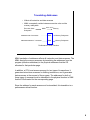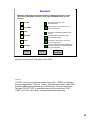
1
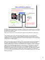
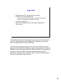
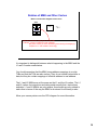
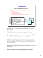
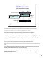
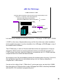
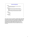
Course Introduction
Purpose:
• This course examines the structure and functions of the e500 MMU
architecture.
Objective:
• Define and explain MMU concepts.
• Identify the MMU needs for embedded applications.
• Explain Book E architectural definitions.
• Examine e500 MMU details.
Content
• 50 pages
• 8 questions
Learning Time
• 1.25 hours
Welcome to the e500 Memory Management Unit (MMU) course. This course
examines the e500 MMU architecture and describes its structure and
function.
We will begin by defining and explaining MMU concepts and identifying the
MMU requirements for embedded applications. Next, we will explain the
Book E architecture and further definitions of that architecture. Finally, we
will examine the e500 MMU details.
1
Addressable Physical Memory
Mouse over the L2 and L3 caches and the RAM block to learn more.
Typically, the caches closest to the CPU are the fastest
(and most expensive); therefore, they are the smallest.
Then, there is a hierarchy of caches that increase in size as
they decrease in cost (and increase in access times).
CPU
fetch
Physical (Real)
LSU
0
Pages or Blocks
RAM
MMU
L2
IL1
L3
DL1
•
•
Program addresses
A0
A31
0000_0000
OS
•
07FF_FFFF
128M
RAM is slower, but considerably cheaper
than the memories used for caches, and
the total amount of RAM is typically less
than the full memory range allotted to the
software.
•
•
FFFF_FFFF
•
4G
A typical computer system uses a hierarchy of different types of memory that is invisible to
the application software. Closest to the CPU is a hierarchy of caches. Caches are usually
filled on an as-needed basis.
Move your mouse pointer over the L2 and L3 caches and the RAM block to learn more.
The operating system (OS) treats the system RAM as cache for the actual image of
memory on the disk. However, instead of replacing individual entries in RAM on an asneeded basis, it loads the RAM with chunks of memory called pages or blocks as required.
This OS action is called “paging”.
When the OS brings a page into RAM from disk, it must assign a physical base address to
the page. This physical address is the address encoding that the CPU drives on the
address signals that are connected to the RAM devices in hardware in order to access the
page. This scheme allows each program to use memory as if it had access to the entire
memory space, which is 4 GB in the case of 32-bit addresses. However, most often
programs are running out of a much smaller amount of RAM. This type of system is called
a “Demand Paged Virtual Memory” system, and it requires a scheme for informing the
CPU of the actual physical address bits to drive onto the hardware signals when accessing
RAM for each page.
2
Multiple Tasks
CPU
Pages or Blocks
fetch
LSU
RAM
MMU
L2
IL1
L3
DL1
A0
A31
A:
addi
128M
OS
bne
•
•
B:
ld <ea>
fmul
•
4G
A second function that is useful in many computing applications is for
multiple programs to have pages mapped into RAM at the same time. Note
that this means that both program and data addresses must be mapped.
3
Definition of MMU
Memory Management Unit (MMU):
“A way for the operating system to
manage the memory map for
instruction and data accesses”
Has to do with where things are...
the addresses of code and data and
the translation of addresses
Here you can see a definition for MMU. This idea of paging in blocks or
pages into RAM is an OS concept—the OS is the boss. However, for
performance reasons, we don’t want the OS to be involved directly with each
and every access. Thus, most processors have dedicated hardware to help
perform these tasks. The purpose of MMU circuitry in the CPU is to help the
OS allocate the space in RAM, keep track of it, and actually translate the
addresses as memory accesses are needed.
4
Software Concept
• MMU: start with a software model
• OS concept
But, processor hardware can help.
MMU Strategy
Helpful Resources
Allocate Memory
OS
Keeps Track
Fast xlation
Port
Protection
Processor
OS must be ported to a processor architecture.
The OS sets everything up, and the hardware performs the translation for
each access. Let’s examine how the OS can best use those helpful
resources.
5
Translating Addresses
• Affects all instruction and data accesses
• MMU conceptually resides between execution units and the
memory subsystem.
Execution Units
Subsystem
MMU
Where to Go*
Memory
Load/store unit: d-accesses
MMU
Memory Subsystem
Instruction fetch unit: i-accesses
MMU
Memory Subsystem
Performance-Critical Function
MMU translation of addresses affects all instruction and data accesses. The
MMU directs the memory accesses by translating the addresses from the
program (effective addresses) to the physical addresses that the OS
allocates for that particular page.
In addition, a CPU must access memory for two types of transactions. It
generates instructions accesses for fetching instructions, and it generates
data accesses at the request of the program. The addresses for both of
these types of accesses must be translated to the physical location in RAM
that the OS allocated for the corresponding page.
Since the address for each access must be translated, this translation is a
performance-critical function.
6
Question
What is the purpose of MMU circuitry in the CPU? Select the
correct answer and then click Done.
a. Only to help the OS allocate the space in RAM
b. Only to translate the addresses as memory accesses are needed
c. To help the OS allocate the space in RAM, keep track of it, and actually
translate the addresses as memory accesses are needed
d. To help the OS allocate the space in caches, keep track of it, and actually
translate the addresses as memory accesses are needed
Consider this question about the role of MMU circuitry.
Correct.
The purpose of MMU circuitry in the CPU is to help the OS allocate the
space in RAM, keep track of it, and actually translate the addresses as
memory accesses are needed.
7
MMU Functions
Address translation
– Implements virtual memory—program has full address range
(page from disk to RAM)
– Multiple programs may have the same logical address range
simultaneously
– Dynamic management of RAM (paging)
Protection: privilege control
– Protects supervisor areas from user-level programs
– Prevents one task from disturbing another task’s memory area
Impose other controls on page basis
– Allows I/O accesses to be non-cacheable while allowing other
areas to be cacheable
– Prevents loss of data from speculative destructive reads while
allowing speculative reads from other memory areas
– Allows selected memory areas to be read-only (treated like
ROM)
– Pages can be designated “no-execute”
The MMU also assigns other useful attributes to pages. So the MMU assigns
each page a descriptor that includes its logical address, size, current
physical location, access rights and protection attributes, and other attributes
such as whether its cacheable. Let’s look at the three functions that an MMU
can perform: address translation, protection, and imposing other controls on
a page basis.
Here you can see that that the MMU address translation function implements
virtual memory, so programs can use the full address range. In addition,
multiple programs may have the same logical address range simultaneously,
and the MMU uses dynamic management of RAM.
The MMU protection function protects supervisor areas from user-level
programs and prevents one task from erroneously or maliciously disturbing
another task’s memory area.
The MMU functions also include imposing other controls on a page basis. It
allows input/output (I/O) accesses to be non-cacheable while allowing other
areas to be cacheable. The MMU also prevents data loss from speculative
destructive reads (status flags) while allowing speculative reads from other
memory areas. Selected memory areas can also be designated read-only.
Finally, this MMU function allows pages to be designated “no-execute.”
8
e500 Address Translation
CPU
fetch
LSU
MMU
IL1
Logical Address
(Effective)
(Program)
32-bit
DL1
Virtual Address
41-bit
Physical Address
(Real)
32-bit
In the case of the e500, the MMU resides in between the execution units and
the L1 instruction and data caches. The MMU hardware for the e500 creates
an intermediate address called the virtual address, which also contains
process identifying information, before creating the final physical address
used when accessing external memory.
9
Page Table
• Managed by the OS—data structure in memory
• Location of all current translations
– Effective to physical address mappings in page table entries (PTEs)
– Each PTE corresponds to the translation for a page.
• Could be a huge table
• Must avoid invoking OS just to get address translation of
every access
The descriptors that describe the pages, as set up by the OS, are stored in
memory in a data structure called a page table. Depending on the page
sizes, this page table structure could be huge.
The OS maintains the page table for each task and provides the relevant
information to the MMU so the MMU can perform the translations. When the
MMU encounters an address for which it has no information, it generates an
exception to invoke the OS to supply the needed information prior to
continuation of the translation. However, we don’t want to invoke the OS to
access the page table for every access.
10
TLBs
On-chip Translation Lookaside Buffers (TLBs)
32-bit Effective Address
EA[0:19]
(Generated by Instruction
Fetch or Data Access)
32-bit Real Address
RA[0:19]
L1 cache(s)
Low-order 12 Address Bits (EA[20:31])
Used in Parallel for L1 Cache Lookup
Instructions or Data
One of the functions of an MMU is to perform address translation. A 32-bit effective
address is generated by an instruction fetch or a data access. Address translation is
always enabled with a Book E device, so every access must be translated.
It is necessary to have On-chip Translation Lookaside Buffers (TLBs) that are
essentially caches of these translations or mappings.
On the right side of the diagram, you can see that we end up with a 32-bit real
address. Ideally, these translations are on-chip and are performed in parallel with
the L1 cache lookups.
In the case of the e500, there is an L1 instruction cache and an L1 data cache that
hold instructions and data respectively. The address translation for that access is
performed in parallel with the L1 cache access. The L1 caches are physical caches,
so they need the translated address before they can complete the access. The
lower order address bits are used to begin the index into the L1 caches, which
takes up most of the access time. Then, at the very last moment when we have
performed our translation, we have our upper order address bits from the address
translation. We compare those with the corresponding bits in the L1 cache, and we
know whether or not we have a hit in the L1 cache.
11
Embedded Needs
Flexible, Efficient, and Deterministic
• Do it in software
– Directly manages TLB and its hit rate
– Allows a simple system with low overhead
– Allows for a more deterministic system
• Opportunities for performance improvement
– Minimize use of TLBs by OS
– Hand-optimize MMU exception handlers and page fault code
• Book E/e500 MMU features
–
–
–
–
–
–
–
16 page sizes (1 KB to 1 TB); 9 page sizes (4 KB to 256 MB)
Page tables defined completely by OS
TLB entry cache attribute fields (WIMGE) and U0–U3
TLB instructions: tlbre, tlbwe, tlbivax(e), tlbsx(e), tlbsync
TLB miss interrupts (ITLB error and DTLB error)
6 on-chip TLBs for high-hit rates
Defaults defined for TLB miss interrupts equals easy and fast
exception handling.
For embedded applications, we need a simple and efficient method for
maintaining the page tables and for loading the TLBs directly. Softwaremanaged TLBs allow you to have a simple, more deterministic system that
directly manages the TLB and its hit rate.
We want to maximize performance, so we should maximize the hit rates of
our TLBs for our application software. This involves minimizing the use of the
TLBs by the OS, and may involve hand-optimizing the exception handling
code that loads the TLBs.
Here you can see some of the reasons why Book E MMU architecture and
the e500 implementation are very well suited for embedded applications.
The e500 gives the OS the tools it needs to efficiently manage the page
tables and the TLBs. Also, the e500 has extensive on-chip hardware
resources dedicated to high hit rates in the TLBs.
12
Question
Match each MMU function to its description by dragging the letters on the
left to their corresponding descriptions on the right. Each letter may be
used more than once. Click Done when you are finished.
A Address translation
B
Protection: privilege
control
C Impose other controls on
page basis
Done
B
Protects supervisor areas from user-level programs
A
Implements virtual memory—program has full address
range (page from disk to RAM)
B
Prevents one task from disturbing another
task’s memory area
C
Prevents loss of data from speculative destructive
reads while allowing speculative reads from other
memory areas
C
Allows I/O accesses to be non-cacheable while
allowing other areas to be cacheable
Reset
Show
Solution
Let’s review the MMU functions.
Correct.
Address translation implements virtual memory—program has full address
range. Protection: privilege control prevents one task from disturbing another
task’s memory area and protects supervisor areas from user-level programs.
Impose other controls on page basis prevents loss of data from speculative
destructive reads while allowing speculative reads from other memory areas
and allows I/O accesses to be non-cacheable while allowing other areas to
be cacheable.
13
Performance Considerations
• Page table search time (worst case)
• TLB hit rates —TLB misses are expensive
– Small changes can have a big impact on overall system performance
– TLB must be invalidated in some circumstances
• OS operations impact
• Page fault service time
– Frequent actual page faults (unavoidable with paging scheme)
– Page faults caused by hot spots in page tables (no room for PTEs)
• OS adaptability—Ex: PowerPC Linux uses a 2-level page table tree
and PowerPC page tables serve as a “cache” of this structure.
When you look at an MMU environment, there are some performance considerations you
need to think about for an embedded application. First, you need to be concerned about the
worst case page table search times.
The on-chip TLB hit rates are absolutely vital. A TLB miss can be expensive and small
changes in hit rates can have a very big impact on the overall system performance.
Another factor that affects the TLB hit rate is the invalidation that is required when mapping
new addresses into the process or when an OS dynamically links in a new process and must
re-map to use shared libraries.
You also have to consider the effects of the OS on the TLB. OS functions can cause TLB
thrashing and on-chip I and D cache thrashing.
When you page a new chunk of memory into RAM, you have to consider how long it takes.
You might have a situation where you run out of room for the PTEs in the page table.
The adaptability of operating systems is also a concern. Typically, operating systems have
their own structures already defined for maintaining recently used or already defined page
table entries.
14
Book E MMUs and Implementations
Three Levels of Definition
•
•
•
Book E architecture
– 64-bit with lots of architectural flexibility
Freescale Book E Implementation Standard
– More programming details defined
Actual cores and devices
– e500 core defines many more details about TLBs
Within that flexibility, Freescale has decided to publish some of the common
features that will be present in all Freescale Book E devices. We call this the
Freescale Book E Implementation Standard. It provides more details about
the MMU structure for all devices that implement Book E for Freescale.
The e500 core defines many more details about TLBs. We will examine the
e500 core specifically and the particular hardware features that it supplies
later in this course.
15
Book E MMU Definitions
•
•
•
•
•
•
•
•
•
64-bit effective address range
16 page sizes (1 KB – 1 TB)
Page tables defined by OS
Address space concept (MSR[IS] and MSR[DS])
Process ID—prevents need to flush entire TLBs on task switch
Combined I and D translation mechanism (prog. model)
TLB fields:
– TLB entry page identification fields [V, AS (TS), PID (TID), EPN]
– TLB entry translation field (RPN)
– TLB entry access control fields (permissions)
– TLB entry cache attribute fields (WIMGE) and U0–U3
TLB instructions: tlbre, tlbwe, tlbivax(e), tlbsx(e), tlbsync
Interrupts:
– Permissions violation (subsets of ISI, DSI), and TLB miss (ITLB
error, and DTLB error)
The MMU for a Book E device is defined as a 64-bit address range with multiple page sizes, from 1 KB to 1 TB. The structure of the
page tables is completely defined by the OS.
There is a concept called the Address Space, which is defined by two bits in the Machine State Register (MSR): the IS bit and the
DS bit. The IS bit is the address space bit for instruction accesses and the DS bit is the address space bit for data accesses. You
should note that this essentially assigns one more bit to the effective address for every access. Note that address translation is
always enabled in a Book E device.
Another concept is the Process ID (PID), which allows you to assign more bits that the OS will use to identify a particular process
and add that onto the effective address as part of the virtual address. The PID is saved in the on-chip TLBs, which allows you to
have TLB entries on-chip that belong to multiple processes. Since the PID is saved along with the rest of the TLB information, you do
not have to flush out the TLBs when you have a task switch.
The TLB fields that are defined at the Book E level are the Valid bit (V), the Address Space bit (AS), the Translation Space bit (TS),
and the TID bit. We compare the AS with the TS on-chip and we compare the PID with the TID of the TLB entry on-chip. The
effective page number (EPN) is one more TLB entry page identification field.
Another TLB field is the Real Page Number (RPN) entry translation field.
There are also entry access control fields (permission bits) that allow execute protection and a read protection and write protection.
Cache attribute fields are applied to each particular page. You can see that we have the WIMG bits from PowerPC Classic with
essentially the same definition, but an additional bit called the E bit has been added, and it controls the Endianess of that page or
accesses within that page for every page. The E bit controls whether the page is to be treated as big Endian or little Endian. Four
bits are also available for use by the OS.
Five TLB instructions are defined by Book E. They are the TLB Read Entry (tlbre), TLB Write Entry (tlbwe), tlbivax, tlbsx, and tlbsync.
Tlbivax is an invalidate instruction for invalidating TLB entries. Tlbsx is a search instruction and tlbsync allows us to synchronize TLB
accesses for a multiple core or a multiple processor kind of environment.
Book E also defines four interrupts that are related to MMU functions. Two of them are the TLB miss exceptions or interrupts. They
are Instruction TLB Error and Data TLB Error. There are also the ISI and DSI exceptions, which are present in PowerPC Classic.
When there is a permission violation in the MMU, we take either an ISI or a DSI exception.
16
Page Sizes
Book E
1
4
16
64
256
1
4
16
64
256
1
4
16
64
256
1
e500
(Classic BAT)
KB
MB
4
16
64
256
1
4
16
64
256
KB
MB
GB
128
256
512
1
2
4
8
16
32
64
128
256
KB
MB
TB
Now, let's look at the different page sizes.
We mentioned previously that there are variable page sizes with Book E.
These pages range in size from 1 KB to 1 TB.
In this version of the e500, we can only implement nine page sizes. These
nine pages range in size from 4 KB to 256 MB.
When you see the PowerPC Classic block address translation (BAT) sizes
next to the e500, think of the e500 as having 4 KB pages like PowerPC
Classic. We can define large areas like Classic BAT areas from 128 KB to
256 MB. The only difference is that we do not have 128 KB size in the e500.
The page sizes go up by powers of 4 on the e500, whereas in the Classic
BAT areas, they increase by powers of 2.
17
Question
Is the following statement true or false? Click Done
when you are finished.
“The variable page sizes in Book E range from 4 KB to 256 MB.”
True
False
Done
Consider this question regarding the variable page sizes in Book E.
Correct.
The variable page sizes in Book E are 1 KB to 1 TB. The nine pages in the
e500 range in size from 4 KB to 256 MB.
18
Relation of MMU and Other Caches
Mouse over the CPU diagram to learn more.
CPU
fetch
LSU
L2
Cache
MMU
IL1
DL1
• MMU stores address mappings in on-chip TLBs.
• TLBs are “caches” of effective to real mappings.
- May have a variety of cache structures (just for storing the mappings)
- Prepare for “L1 and L2 MMU” terminology
It is important to distinguish between what is happening in the MMU and the
L1 and L2 cache nomenclature.
You should remember that the MMU stores address mappings in on-chip
TLBs and that the TLBs are also caches. They do not contain instructions or
data, but they do contain mappings of effective address to real address.
The L1 and L2 MMUs are not the same as the L1 and the L2 caches. The L1
and L2 caches for instructions and data contain exactly that—instructions
and data. L1 and L2 MMUs are only relative; those levels are only related to
each other in terms of the way the MMU is structured for efficiency’s sake.
Move your mouse pointer over the CPU diagram for more information.
19
e500 Address Translation
Effective Address
(Program)
(Logical)
32-bit
Virtual Address
1 + 8 + 32 bits
[AS PID EA]
Real Address
(Physical)
32-bit
We mentioned previously that we have a 32-bit effective address, which is
sometimes called a program address.
We concatenate the PID, which in the case of the e500 is 8-bits, plus the
Address Space bit obtained from the MSR, IS or DS, which gives us 41 bits
of virtual address.
Then, we translate the virtual address to a 32-bit real address.
20
e500 TLBs and Translation
•
Based on the setting of the SIZE field of the matching TLB entry, the RPN field
replaces the corresponding most-significant n bits of the effective address.
MSR[DS] for data access
MSR[IS] for instruction fetch
32-bit Effective Address
PID0
AS
PID1
PID2
0
Effective Page Number (EPN) Offset
n–1 n
31
Three 41-bit Virtual Addresses (VAs)
TLBs
RPN field of matching entry
0
Offset
Real Page Number (RPN)
n–1 n
31
NOTE: n = 32 – log2 (page size)
32-bit Real Address
This diagram shows how the address bits get translated with the e500 MMU.
Since there are variable page sizes, a variable number of bits are translated.
We concatenate the effective address with the current PID value and the
Address Space value, and we use that virtual address, a variable number of
the upper address bits for the comparison. We check all of those bits with
the on-chip TLB entries. Then, in the case of a hit, we get the RPN as our
output. The number of bits that are translated depends on the size field of
the matching TLB entry.
21
Book E Address Spaces
Construction of Virtual Address
• Every effective address (instruction or data) generated has an
additional “address space” bit associated with it.
MSR[IS]
0
63
+ instruction effective address <ea>
0
1
MSR[DS]
0
+
0
63
data effective address <ea>
1
• Note that MSR[IS,DS] are both cleared on interrupts.
– Could be used to separate interrupt areas (or system areas) from user
areas
Let's look at the Address Space bit in more detail.
Every instruction or data effective address generated has an additional
address space bit associated with it.
You should note that the MSR (IS and DS) bits are both cleared on
interrupts. The 00 space of IS Address Space 0 and DS Address Space 0,
can be used as a place to keep mappings for interrupt or OS areas and you
can set the IS and DS bit when you are going to user tasks. That way, user
mappings and interrupt mappings can both be resident on-chip and you can
distinguish between them. Because we are comparing the IS or DS bit, we
do not have to worry about the user and the OS mappings aliasing with each
other but we can still keep them both resident without having to flush one
when we go to the other.
22
Book E Process ID
Construction of Virtual Address (continued)
Mouse over the diagram to learn more.
0
PID register
xxxx_xxxx
+
63
effective address <ea>
•
Every effective address (instruction or data) also has a
process ID value associated with it.
•
Set up by OS to differentiate between tasks.
•
Process ID is saved in TLB entries. Therefore, not all TLB entries must be
flushed on a task (process) switch.
•
PID can be ignored by TLB entries (TID = 0), for sharing of TLB entries.
Since the PID is compared with the TID in the on-chip TLBs, we do not have
to flush the TLBs every time we have a task switch.
The Book E architecture states that when a TLB entry has the TID value
equal to all zeroes, then that entry is automatically compared with the
effective address of every access. It essentially says that there is no
comparison with the current PID. So a TID value of 0 in the TLB entry is not
compared with the PID value as it will match with every PID value. Since it is
a global match, it can be used for TLB entries that we want to share among
all tasks.
Move your mouse pointer over the diagram for more information.
23
Question
Which of the following statements are true regarding the Book E
Process ID? Select all that apply and then click Done.
Every effective address also has a process ID value associated with it.
All TLB entries must be flushed on a task (process) switch.
Process ID is set up by the OS to differentiate between tasks.
Process ID is saved in TLB entries.
PID can be ignored by TLB entries (TID = 0) for sharing of TLB entries.
Done
Consider this question regarding the Book E Process ID.
Correct.
Every effective address also has a process ID value associated with it. The
Process ID is set up by the OS to differentiate between tasks and is saved in
TLB entries. The PID can be ignored by TLB entries (TID = 0) for sharing of
TLB entries. However, not all TLB entries must be flushed on a task
(process) switch.
24
TLB Comparison
• Compare attributes of access with all TLB entries
TLB_entry[V]
TLB_entry[TS]
AS (from MSR[IS]or MSR[DS])
Current Process ID (PID) (s)
TLB_entry[TID]
TLB entry matches EA
=?
=?
Private Page
=0?
Globally Shared
TLB_entry[EPN]
EA page number bits
=?
• Compare effective address of access with all TLB entries
How do we determine an address translation for an access?
We get an address translation hit in an on-chip TLB entry. These are the
compare functions that are performed. We compare the IS or DS bit,
depending on whether we have an instruction or data access, with the TS bit
of all TLB entries.
The current PID is compared with the TID value of every TLB entry.
If the TID value is 0, that entry is globally shared and does not get compared
with the PIDs.
Then, most importantly, we check the effective address bits of the access
with the EPN bits of the TLB entry in question. For all of those compare
functions that result in 1’s, we know that particular TLB matches with the
effective address of that access.
We check that the TLB entry we are looking at has the Valid bit set.
25
Permissions Checking
•
Selected TLB entry provides the access permission bits (UX, SX, UR, SR,
UW, SW), and memory/cache attributes (U0, U1, U2, U3, W, I, M, G, and E)
for the access
TLB Match
MSR[PR]
Access Granted
Instruction fetch
TLB_entry [UX]
TLB_entry
[SX]
load data access
TLB_entry [UR]
TLB_entry [SR]
store data access
TLB_entry [UW]
TLB_entry [SW]
Next, we have to compare whether or not that access has permission to access that page.
We check that the UX bit and SX bits compare whether or not we have User Execute
Permission allowed or Supervisor Execute permission allowed.
UR and SR determine whether or not we have User Read access or Supervisor Read access.
UW and SW determine whether or not we have User Write access or Supervisor Write access.
For example, if we look at that first And Gate and the MSR bit is set, which means we are in
User Mode and it is an Instruction Fetch, we need to make sure that the User Execute bit is
set. If it is, then we know that we get a 1 out of that And Gate and the access is granted.
Next, the second set of bits U0 through U3 and the WIMGE bits from the matching TLB entry
are assigned for that access, and they give us the cache or Memory Attributes for that
particular page; whether or not it is cacheable, whether or not memory coherency needs to be
maintained, and the Endianess.
26
Freescale Book E
Address Translation:
• Multiple PID registers (15) defined for sharing among tasks
– All PID registers are compared with the TID field of all candidate TLB
entries
• MMU assist (MAS0–MAS6) registers used by tilbre, tlbwe, tlbivax(e),
tlbsx(e), instructions to access (set up) TLB entries.
– Software-managed TLBs gives total flexibility to the OS
• TLB arrays
– IPROT field defined for preventing invalidation with tlbivax
Up until now, we have been talking about concepts defined by the Book E architecture. Now, let's
examine the Freescale Book E Implementation Standard and see how it provides more details about
MMU implementation in Freescale devices.
In Freescale Book E devices, there can be multiple PID Registers, whereas Book E defined just one PID
Register. Freescale Book E allows devices that have up to 15 PID Registers for sharing among tasks.
Multiple PID values allow the sharing of TLB entries for pages that are shared among multiple execution
contexts.
For example, you can assign PID 0 to contain the unique PID for private mappings for the current
processes and assign PID 1 to contain the unique PID for a common set of shared libraries. Therefore,
you could have the mappings for both processes available in the on-chip TLBs.
Another feature that is defined at the Freescale Book E level are the MMU Assist (MAS) Registers MAS0
through MAS6. You may recall that Book E does not define much about how these TLB instructions
work—it just defines the opcodes. At the Freescale implementation standard level, the MAS Registers
are how you write TLB entries on-chip. We will examine how to set up the TLB entries in software later in
this course.
Another feature that is defined at the Freescale Book E level is the IPROT field in a TLB entry that can
be defined for preventing invalidation. The tlbivax instruction invalidates TLB entries. You can define an
entry as protected from invalidation from tlbivax with IPROT.
27
TLB Entry Invalidations
TLB entries can be invalidated in one of the following
ways:
• As the result of a tlbwe instruction that clears the valid bit in the entry
• As a result of a tlbivax instruction
• From a received broadcast invalidation resulting from a tlbivax on
another processor in an MP system
• For e500, flash invalidate operation initiated by writing to bits in
MMUCSR0
There are many ways to invalidate TLB entries for Freescale Book E
devices.
You can execute a TLB write entry instruction clearing the valid bit in the
entry.
You can execute the tlbivax instruction.
In a multiple core or multiprocessing system, a tlbivax instruction on another
processor can be broadcast to other cores or processors in the system to
cause an invalidation.
On the e500 device, you can also perform a FLASH invalidate operation by
writing to some bits in the MMU CSR0 Register.
28
Generous Invalidations
•
tlbivax invalidations (or invalidations from tlbivax broadcasts from other
processors) can occur on a wider set of TLB entries than specifically intended.
•
Use of a tlbwe instruction is guaranteed to invalidate only the addressed TLB
entry.
•
Sometimes need to protect against generous invalidations.
•
Certain effective memory regions must be properly mapped at all times. For
example, the instruction memory region that serves as the exception handler for
MMU faults must always be mapped.
Sometimes you may get generous invalidations when invalidating TLB
entries. You need to be aware that the tlbivax instruction invalidates more
TLB entries than the ones specifically intended, and this has to do with the
way the TLBs are structured.
This is called generous invalidation, but another way to look at it is as a kind
of collateral damage. Although we intend to invalidate one entry, we will
definitely invalidate other entries. However, Since the TLB hit rate is
important for performance, the generous invalidations can negatively impact
it. Also, it can effect the ability of our program to be deterministic.
Sometimes, we need to protect against generous invalidations. We need to
know we have loaded a TLB entry on-chip and be absolutely certain that it is
still there.
For example, the area of memory that maps the exception handlers or the
exception vectors needs to be mapped at all times, so you need to make
sure that it does not get invalidated with these generous invalidations.
29
IPROT Bit for TLB Entries
•
IPROT protects an entry from:
– Invalidations resulting from tlbivax instructions
– tlbivax broadcasts (from another processor in an MP system)
– Flash invalidates initiated by MMUCSR0 settings
•
TLB entries with the IPROT bit set can only be invalidated by explicitly writing
the TLB entry and specifically clearing the valid bit.
•
Operating systems need to use great care when using protected TLB entries,
particularly in MP systems.
•
Note that not all TLB arrays in a given implementation have IPROT capability.
The answer to the problem of generous invalidations is the IPROT bit for
TLB entries in Freescale Book E devices.
The IPROT bit protects an entry from certain invalidate operations.
However, you can still invalidate an entry that has IPROT set by explicitly
writing the TLB entry or clearing the valid bit.
Operating systems need to use great care when using protected TLB
entries. If you overuse IPROT, you may have so many protected entries that
you have fewer TLB entries available for tasks and even the OS. This
situation could negatively affect your TLB hit rate and dramatically reduce
your performance.
IPROT capability is not required, but it is a feature that is available with
Freescale Book E devices.
30
MAS Registers
Mouse over the MAS Register to learn more.
MAS registers are “conduits” for accessing TLB entries (contain
parameters):
• For writing TLB entries
• For reading/searching TLB entries
• Default values pre-loaded into MAS registers on interrupts
on-chip TLBs
MAS0
TLBSEL, ESEL, NV
Select Entry
MAS1
V, IPROT, TID, TS, TSIZE
MAS2
EPN[0–31], EPN[32–51], X0, X1, WIMGE
MAS3
RPN[32–51],U0–3, UX, SX,UW,SW,UR,SR
MAS4
TLBSELD, TIDSELD, TSIZED, default X0x1, dWIMGE
MAS5
SPID2, SPID3
MAS6
SPID0, SPID1, SAS
tlbwe
Defaults
For Searching
Let's go into a bit more detail regarding the MAS Registers of Freescale
Book E devices.
The MAS Registers are like conduits for accessing the TLB entries.
You load up the parameters that you want to put in a TLB entry into MAS0
through MAS3. For a TLB write entry instruction, those bits select and define
the entry and then load it into the appropriate on-chip TLB.
MAS 4 is very useful because you can set it up with a number of default
fields. If you set those default fields correctly, it can greatly simplify the set
up of new Page Table Entries, or TLB entries for a Demand Paged Virtual
Memory environment.
MAS5 and MAS6 are important when searching for a TLB entry in one of the
on-chip TLBs.
Move your mouse pointer over the MAS register for more information.
31
Question
Which of the following are Freescale Book E features? Select all
that apply and then click Done.
Multiple PID registers are defined for sharing among tasks.
Software-managed TLBs gives total flexibility to the OS.
MAS5 is used only for writing TLB entries; MAS3 is used to search for a
TLB entry in one of the on-chip TLBs.
The IPROT field in a TLB entry can be defined for preventing invalidation.
Done
Consider this question regarding Freescale Book E features.
Correct.
Multiple PID registers are defined for sharing among tasks. Softwaremanaged TLBs gives total flexibility to the OS. The IPROT field in a TLB
entry can be defined for preventing invalidation. MAS5 is actually used to
search for a TLB entry in one of the on-chip TLBs, and MAS0 through MAS3
are used to load up the parameters into a TLB entry, including writes.
32
e500 Implementation Details
Effective Address
32-bit
3 Virtual Addresses
1 + 8 + 32 bits
“ + 8 + “ bits
“ + 8 + “ bits
0
7
PID0
ex:Task A
PID1
ex: Libraries
PID2
ex: OS
Real Address
32-bit
on-chip TLBs
3 current PIDs
Now, let’s examine the third level of definition for the e500. These are the implementation details that are defined
for the e500 itself.
You should note that while Book E is defined to account for 64-bit effective addresses, the e500 is a 32-bit device.
The e500 translates 32-bit effective addresses into 32-bit real addresses.
The e500 also implements three PID Registers, so you can have on-chip at any time, three 8-bit PID values that
get compared with every TLB entry to see if you have a hit.
The three PID values are used to construct three virtual addresses for every access, and any one of those
addresses can hit in the TLB entry for that access.
This is an example where PID 0 might have the mappings that correspond to the mappings for a particular task.
PID 1 could have mappings for shared libraries.
And PID 2 might have mappings for other OS functions that need to be available to Task A.
All three current PIDs are considered the current process.
33
e500 Implementation Details
Mouse over the bulleted point to learn more.
• SHAREN attribute (in addition to WIMGE)
– Designates pages as shared or not, with respect to the memory/cache
subsystem:
0 = MEI cache coherency model
1 = MESI cache coherency model
– L1 data cache misses cause either a normal read (0) or RWITM (1)
transaction on core complex bus
on-chip TLBs
. . . TLB[SHAREN]
Another feature of the e500 is that in addition to the WIMGE bits, there is an
additional bit called the SHAREN Cache Attribute bit that can be determined
by the OS on a page basis.
What do we mean when we say that the OS can determine the SHAREN
Cache Attribute on a page basis? The OS assigns this bit to reflect whether
or not the memory/cache subsystem is using the MEI protocol or the MESI
Cache Coherency protocol; or whether or not the L1 Caches implement the
shared state.
Move your mouse pointer over the bulleted heading for more information.
34
e500 MMU Implementation
Effective to Real Translation: On-chip TLBs
15–20 bits
32-bit Effective Address (EA) Effective page number
4
2
L2 MMU (unified)
>12 bits
Byte address
L1 MMUs (instr. or data)
4-entry fully-assoc. arrays (2)
64-entry 4-way set-assoc. arrays (2)
16-entry fully assoc. array (TLB1)
256-entry 2-way set assoc. array (TLB0)
15–20 bits
32-bit Real Address
Real page number
2-level
MMU struct:
(L1 is
“invisible”)
>12 bits
Byte address
To understand how the e500 device works you need to pay very close attention to the following details.
The e500 has six on-chip TLBs. These on-chip TLBs are highlighted in the diagram.
The six TLBs are caches and they are organized with an L1 hierarchy and then an L2 hierarchy.
At the L1 level, the TLBs are divided into instruction access resources and data access resources. There are two
L1 TLBs for instruction accesses and two for data accesses.
At the L2 level, the TLBs are unified for instructions and data and there are two different kinds of TLBs at this
level.
There are, at the L1 level, two fully-associative arrays and two 4-way set-associative arrays.
At the L2 level, there is one 16-entry, fully-associative array (TLB1) and one 256-entry 2-way set-associative array
(TLB0).
It is very important to note that the L2 MMU is the only one that is accessible to the software. When TLB entries
are loaded, they are loaded into the L2 MMU. That is all you can control.
The L1 MMUs are faster and smaller than the L2 MMU. They are closer to the execution units and they are
essentially invisible to the software other than having faster performance. The L1 MMUs are completely
maintained automatically by the core.
35
Relation of MMU and Other Caches
CPU
fetch
LSU
L2
Cache
MMU
IL1
DL1
• MMU stores address mappings in on-chip TLBs.
• TLBs are “caches” of effective to real mappings.
– May have a variety of cache structures (just for storing the mappings)
– Prepare for “L1 and L2 MMU” terminology
Let's look at this diagram again as a reminder that when we are describing
the L1 and L2 MMU, we are not referring to the L1 and L2 Caches on-chip.
We are describing an efficient way to maintain these mappings within the
MMU.
36
e500: Two Levels of MMUs
Consistency Between L1 and L2 TLBs
•
L1 MMU arrays are reloaded using entries from their L2 array equivalent.
– If L1 data MMU misses, but hits in TLB1 (the 16-entry VSP L2 TLB), that entry is
automatically loaded into the data L1VSP array.
– If the L1 data MMU misses, but hits in TLB0 (the 256-entry TLB for 4-KB pages),
that entry is automatically loaded into the data L1TLB4K array.
<ea>
4
L1 MMUs
MAS Registers
2
“Invisible”
I-L1VSP
D-L1VSP
I-L1TLB4K
D-TLB4K
L2 MMU (unified)
16-entry VSP (TLB1)
256-entry 2-way set assoc. array (TLB0)
<ra>
This diagram provides more details regarding the six TLBs: in the L2 MMU, a 16-entry fully-associative array (TLB1) and a 256-entry 2-way setassociative array (TLB0); and in the L1 MMU, two 4-entry fully-associative arrays and two 64-entry 4-way set-associative arrays.
The L2 MMU is accessed through the MAS Registers. Remember, the MAS Registers are the conduits or the mechanism for writing to the on-chip
TLBs. The only way to access the L2 MMU is through the MAS Registers.
The L1 MMUs are invisible to the software. The L2 MMU access time from the core is 5 clocks for an instruction cache access and 6 clocks for a
data cache access. These are very high performance TLB arrays that have very high hit rates. Because they are relatively large in size, these arrays
do not have the 1 clock access time we would like, but these are the ones that we can control in the software. In designing this core, it was useful to
implement a subset of the contents of the L2 MMU in resources that are more accessible to the core with a 1 clock access time (the L1 MMUs).
Naming the six TLBs can help you to keep track of them. In the L2 MMU, there is a 16-entry, Variable Size Page (VSP) TLB. This TLB is called
TLB1, and it can keep resources for variable size pages from 4 KB to 256 MB in size. It is very important for you to remember the name TLB1.
A second TLB in the L2 MMU is called TLB0. TLB0 is a 256-entry TLB that can only keep translations for 4K pages since it is a 4 KB page array.
There are two instruction L1 MMUs, which are named I-L1VSP and I-L1TLB4K. These instruction L1 MMUs always maintain a subset of what is in
the L2 MMU, and they are automatically loaded by the hardware. On the first instruction access, the e500 performs a look-up in parallel in I-L1VSP
and I-L1TLB4K arrays. The first time, they miss. Next, the e500 checks both of the arrays of the L2 MMU (TLB1 and TLB0). If any one of those
arrays hits, the L1 MMU (either I-L1VSP or I-L1TLB4K) is loaded up with a copy of that TLB entry for future use. The diagram shows how the L1
MMUs are loaded; the orange-coded L1 MMUs are loaded from TLB1 and the green coded L1 MMUs are loaded from the TLB0.
It is important to keep in mind that the software model absolutely prescribes that you may never have multiple hits. You have to be careful never to
have written through the MAS Registers two entries in the L2 MMU that could match with a particular access. Because they are unified TLB arrays,
you cannot assume that one matching entry is going to be used for instructions and another matching entry is going to be used for data and have
them overlap the effective address space; they must be distinctly different so that only one entry hits for each access.
Back to our example: we loaded up the L1 cache and the corresponding TLB in the L1 MMU. The next time we access that particular page, we are
going to hit in the L1 MMU with a 1 clock access time, which is incurred in parallel with the L1 Cache Access time. Essentially, we are getting the
translation for free from that point forward.
The same mechanism works for the data accesses. We check both the data L1 MMUs in parallel. If we miss, we check both of the L2 MMU arrays.
We load up, and if one of the L2 MMU arrays hits, we load up into the appropriate D-L1VSP or D-TLB4K. Once entries are loaded into the L1 MMUs,
those instruction accesses and data accesses can both access the L1 MMUs in parallel, in the same clock. It is a very efficient mechanism for
obtaining a high hit rate and fast access time for TLBs and for address mappings.
It is also important to point out that any time an entry is invalidated in the L2 MMU, the hardware automatically invalidates any corresponding entry in
the L1 MMUs. Any time we change any TLB entry in the L2 MMU, we will invalidate that entry in the L1 MMU. The hardware needs to miss in the L1,
go re-fetch it from the L2, and bring it back into the L1. The L1 MMUs are always maintained as proper subsets of their L2 equivalents in hardware.
37
Question
Which of the following are e500 features? Select all that apply
and then click Done.
The e500 translates 32-bit effective addresses into 32-bit real
addresses.
Three PID values are used to construct three virtual addresses for every
access.
In the L2 MMU, the 16-entry, VSP TLB is called TLB0.
The SHAREN Cache Attribute bit is determined by the operating
system on a page basis.
Done
Consider this question regarding e500 features.
Correct.
The e500 translates 32-bit effective addresses into 32-bit real addresses.
Three PID values are used to construct three virtual addresses for every
access. The SHAREN Cache Attribute bit is determined by the OS on a
page basis. In the L2 MMU, the 16-entry, VSP TLB is called TLB1.
38
e500: Six TLB Arrays
L1 MMU: 2 Instruction L1 TLBs
Maximize address translation performance and provide ample flexibility for OS.
• Instruction L1 TLB Arrays: All full LRU replacement
– Instruction L1VSP 4-entry, fully associative
– Instruction L1TLB4K 64-entry, 4-way set associative
2 (of 6) TLBs
I- L1VSP
9 pg sizes
upper bits ea
Hit
0
Memory system:
L1 cache
Miss
index
15
upper bits real address
check L2 MMU
I- L1TLB4K
4 KB pg size
Let’s take a more detailed look at the two instruction L1 TLB arrays: I-L1VSP and I-L1TLB4K.
I-L1VSP is a four-entry, fully-associative array, and the four entries can contain translations
for the variable size pages. It can be a translation for a 4 KB page, a 256 MB page, or any of
the available sizes in between.
The L1TLB4K array or cache is 64-entries and these entries are organized as a 4-way set
associative. When we have an incoming instruction access, we check all four entries of IL1VSP and also use lower order bits to index into one particular set of I-L1TLB4K, and then
compare all those four entries that have that index.
We compare to see if the virtual address matches the remaining bits in the entry. If we do hit,
then we take the upper bits (our real address) and go onto our memory subsystem to
complete the L1 cache access.
If we do not hit in either of the L1 TLBs in the L1 and we get a miss, we check the L2 MMU.
Note that setting up TLB entries that overlap 4 KB pages and VSPs is absolutely disallowed
with the e500—it’s considered a programming error.
39
Book E Address Translation
For e500
On-chip TLBs
32-bit effective address
(Generated by
instruction fetch or data
access)
32-bit real address
L1 cache(s)
Instructions or data
Review this diagram again to remind yourself that we have 32-bit effective
addresses that are generated by instruction fetches or data accesses.
The translation of these bits is performed in parallel with an L1 cache
access. All of this is done invisibly for us in the hardware.
40
e500: Six TLB Arrays
L1 MMU: 2 Data L1 TLBs
•
Data L1 TLB Arrays: All full LRU replacement
– Data L1VSP 4-entry, fully associative
– Data L1TLB4K 64-entry, 4-way set associative
2 (of 6) TLBs
D- L1VSP
9 pg sizes
upper bits ea
Hit
0
Memory system:
L1 cache
Miss
index
15
upper bits real address
check L2 MMU
D- L1TLB4K
4 KB pg size
Now, let's look at the equivalent data L1 arrays: D-L1VSP and D-L1TLB4K.
The Data L1 TLB arrays are essentially identical to the Instruction L1 TLB
arrays. There are four entries for Variable Size Pages, and they are fully
associative, and the 4 KB page entries are organized as a 4-way setassociative. Since the L1 TLB arrays are set associative and fully
associative, the chip needs to decide which entry to replace when they are
all full.
The hardware automatically maintains a full Least Recently Used (LRU)
replacement algorithm for the L1VSP and the L1TLB4K arrays. This is the
case for both the instruction and data arrays. All of this is done invisibly for
us in the hardware.
41
e500: Six TLB Arrays
L2 MMU: 2 Unified L2 TLBs
L2 TLB Arrays: Software replacement algorithms
– TLB1: 16-entry, fully-associative array
– TLB0: 256-entry, 2-way set-associative array
Only TLB entries in TLB1 can be protected; entries in the TLB0 and in the L1
0
MMUs cannot be protected
15
Upper bits ea
Check L2 MMU
(L1 MMU miss)
•
•
•
0
TLB1
9 pg sizes
Replacement algorithm completely implemented
by software
Hit
Miss
index
127
Fill corresponding L1 MMU
INTERRUPT
TLB0
4 KB pg size
Hardware Support for Round Robin
replacement
The arrays that we can directly write to through the MAS Registers are the
L2 MMU arrays: TLB1 and TLB0.
TLB1 is a 16-entry, fully-associative array. TLB1 entries are similar to the
BAT arrays in the PowerPC Classic architecture.
TLB0 maintains 4 KB page translations and its 256-entries are organized as
2-way, set associative. Since these are also set associative, we need to
have a replacement algorithm for selecting entries to replace when we need
to add a new entry. Note that we maintain these arrays in the software.
For the TLB1 array, it is completely up to the software to implement a
replacement algorithm. Once we have already loaded up 16 entries, how do
we know which one to displace the next time we need to add an entry? The
software just needs to implement an algorithm.
In the case of the TLB0, the e500 provides assistance by implementing a
simple round robin replacement algorithm for choosing either Way0 or Way1
when we need to replace an entry in TLB0.
42
Question
Match the TLB arrays to their descriptions by dragging the letters on the
left to their appropriate locations on the right. Click Done when you are
finished.
A
I-L1VSP
C
This TLB is a 16-entry, fullyassociative array.
B
I-L1TLB4K
B
This instruction TLB is a 64-entry, 4way set associative.
C
TLB1
D
This TLB is essentially identical to the IL1VSP.
D
D-L1VSP
A
This instruction TLB is a four-entry,
fully-associative array.
E
TLB0
F
This data L1 TLB array is a 64-entry,
4-way set associative.
F
D-L1VSP
E
This TLB maintains 4K page translations
and its 256 entries are organized as a 2way, set associative.
Done
Reset
Show
Solution
Now let’s review the six TLB arrays of the e500.
Correct.
I-L1VSP is a four-entry, fully-associative array and I-L1TLB4K is a 64-entry,
4-way set associative. TLB1 is a 16-entry, fully-associative array, while TLB0
maintains 4KB page translations and is a 256-entry, 2-way set associative.
The data TLB, D-L1VSP, is essentially identical to the instruction TLB, IL1VSP. D-L1VSP is a 64-entry, 4-way set-associative data array.
43
MMUCFG
Read-only; tells you about the characteristics of this MMU
Bits
Name
Description
32–48
—
49–52
NPIDS
53–57
PIDSIZE
58–59
—
60–61
NTLBS
Number of TLBs. The value of NTLBS is one less than the
number of software-accessible TLB structures that are
implemented by the processor
62–63
MAVN
MMU architecture version number
Reserved, should be cleared
Number of PID registers
PID register size. The 5-bit value of PIDSIZE is one less than
the number of bits in each of the PID registers implemented by
the processor. The processor implements only the least
significant PIDSIZE+1 bits in the PID registers
Reserved, should be cleared
This table provides information about some read-only registers that are on
the e500 device. The description fields tell you such things as the number of
PID registers that are available, the size of the PID registers, the number of
TLBs, and the MMU architecture version number.
44
TLBnCFG
Read-only; tells you about the specific TLBs
Bits
Name
TLB0CFG
TLB1CFG
32–39
ASSOC
0x02: indicates associativity is 2-way
set associative
40–43
MINSIZE
0x1: indicates smallest page size is 4K
0x1: indicates smallest page size is 4K
44–47
MAXSIZE
0x1: indicates maximum page size is
4k
0x9: indicates maximum page size is
256 Mbyte
48
IPROT
0 IPROT not supported
1 IPROT supported
AVAIL
0
Variable-sized pages not
available (MINSIZE==MAXSIZE) (this
could be 1. all page sizes between min
and max are supported)
Page size availability of TLB1
1
Indicates all page sizes between
MINSIZE and MAXSIZE supported
Reserved, should be cleared.
Reserved, should be cleared.
0x100: TLB0 contains 256 entries
0x010: TLB1 contains 16 entries
49
50–51
—
52–63
NENTRY
0x10: indicates associativity is 16
Since there are two software writeable TLBs, read-only configuration
registers can provide you with details about TLB0 and TLB1. The read-only
registers tell you about the associativity of specific TLBs, the smallest page
size, the largest page size, whether or not the IPROT feature is available,
and how many entries it contains.
45
tlbivax rA,rB
(Entry Invalidation)
<ea> = rA + rB Bits
32–51
52–59
60
61
62–63
Meaning
EA[32–51]
reserved
TLBSEL
0 TLB0
1 TLB1
INV_ALL
command
reserved
for either
This table provides additional information to explain how the tlbivax instruction is
implemented. Note that when L2 MMU entries are invalidated, any corresponding
L1 MMU TLB entries are automatically invalidated by the hardware.
The address that is broadcast by the e500 is a “subset” as shown in the table.
This subset address is broadcast to other processors, and it is also used by the
processor executing the tlbivax instruction.
No other information is used for the invalidation. As shown in the table, EA[32–51]
is used to perform the tlbivax invalidation of TLB1 or TLB0 and the corresponding
L1 TLB entries. Also, note that when bit 61 (invalidate all) is set, either TLB0 or
TLB1 is invalidated, depending on the setting of bit 60.
Note that we are not comparing PIDs and we are not using the Address Space
bit. Also, since some of these arrays are set associative, extra entries will be
invalidated, not just the one that we want to find.
46
Actions at Reset
Mouse over the diagram to learn more.
•
•
Initial code in this page
needs to set up more valid
TLB entries (and pages) so
that the program can branch
out of this 4-Kbyte page into
other pages for booting the
OS.
FFFF_FFFC
b FFFF_F000
FFFF_F000
•
•
•
The interrupt vector area
and pages that contain the
interrupt handlers should be
set up so that exceptions
can be handled early in the
booting process.
We have pointed out the fact that translation cannot be enabled, which
means it is always enabled. Therefore, out of reset the MMU could pose a
problem. What is the first access out of reset and how does the boot code
handle the fact that translation is always turned on? What are the default
translations that are used?
In the e500, all of the TLB entries in the L1 and L2 MMUs are flash
invalidated at reset. Then, entry 0 of TLB1 is loaded with a default value.
TLB1 defines for us a 4 KB page. That 4 KB page is mapped 1:1, meaning
that the effective address equals the physical address.
When a Book E device comes out of reset, it performs a fetch from the
highest address, FFFF_FFFC, which is automatically translated with the
default entry. That instruction should be a branch to the beginning of the 4
KB page that is defined. This will provide you with at least a 4 KB amount of
space in which to set up more pages so that you can start to boot the OS.
Move your mouse pointer over the diagram for more information.
47
TLB1 Entry 0
Set at Reset (by default)
Field
Reset
Comments
V
1
Entry is valid
TS
0
Address space 0
TID[0–7]
0x00
TID value for shared (global) page
EPN[32–51]
0xFFFF_F
Address of last 4-Kbyte page in address space
RPN[32–51]
0xFFFF_F
Address of last 4-Kbyte page in address space
SIZE[0–3]
0001
4-Kbyte page size
SX/SR/SW
111
Full supervisor mode access allowed
UX/UR/UW
000
No user mode access allowed
WIMGE
01000
SHAREN
0
Caching-inhibited, non-coherent
Read all lines as exclusive (3-state cache model)
X0–X1
00
Reserved system attributes
U0–U3
0000
IPROT
1
User bits
Page is protected from invalidation
This table shows you what entry 0 of TLB1 looks like out of reset.
It has an Address Space of 0.
It is a 4-KB page size.
It is supervisor read, write, and execute available.
No user mode access is allowed.
The page it defines is caching inhibited, no coherency-required, and the
page is protected from invalidation. You could invalidate it, but then you
would not have any available translation at reset, so you need to be careful
not to invalidate that entry before you set up other entries to use.
48
Question
Is the following statement true or false? Click Done when you
are finished.
“The e500’s read-only configuration registers can provide you with
details about TLB0 and TLB1.”
True
False
Done
Consider this question regarding the e500 read-only configuration registers.
Correct.
The read-only configuration registers can tell you about the associativity of
specific TLBs, the smallest and largest page sizes, whether or not the
IPROT feature is available, and how many entries it contains.
49
Course Summary
•
•
•
•
Needs for embedded MMU applications
Book E, Freescale Book E Implementation Standard, e500 MMU
definitions
e500 MMU details
User’s manual documentation: search for the E500CORERM at
www.freescale.com
This course examined the e500 MMU and its features and functions. We learned that the Book E architecture is
very loosely defined when it comes to the MMU and provides a lot of architectural flexibility.
We also explained the Book E, the Freescale Book E Implementation Standard, and the e500 MMU definitions.
The MMU for a Book E device is defined as spanning a 64-bit effective address range with multiple page sizes,
from 1 KB to 1 TB.
Features defined at the Freescale Book E Implementation Standard level include multiple PID Registers, MAS
registers, and the IPROT field in a TLB entry. The third level of definition for the e500 is the implementation
details that are defined for the e500 itself: the e500 translates 32-bit effective addresses into 32-bit real addresses
and implements three PID values that are used to construct three virtual addresses for every access. Other
features of the e500 are its six on-chip TLBs and an additional bit called the SHAREN Cache Attribute bit.
Finally, we examined in detail the resources on the e500 that implement the MMU. You learned about the
functions of the L1 and L2 MMUs and the e500’s six TLB arrays. We also examined the read-only and
configuration registers that are on the e500 device and learned how the tlbivax instruction is implemented.
Thank you for taking this course. If you would like more information, please refer to the e500 user’s manual
documentation.
50