1
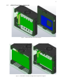
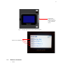
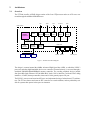
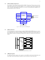
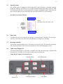
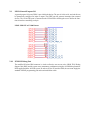
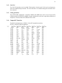
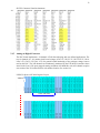
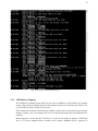
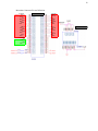
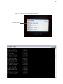
Aeroflex Leon Experimenter’s Interface System (ALExIS) User Guide March 25, 2013 Aeroflex Systems Group 4350 Centennial Blvd. Colorado Springs, CO 80907 2 Table 1. Specification Revision History Date Approved Revision Change Summary 11Mar2012 D. Stevenson New Initial Release 25Mar2013 D. Stevenson 01 Annual Update 3 1 Introduction.............................................................................................................................. 4 1.1 1.2 1.3 1.4 2 Architecture.............................................................................................................................. 7 2.1 2.2 2.3 2.4 2.5 2.6 2.7 2.8 2.9 2.10 2.11 2.12 2.13 2.14 2.15 2.16 2.17 2.18 3 Overview ................................................................................................................................................. 7 LEON 3 SPARC V8 processor................................................................................................................ 8 Memory interfaces................................................................................................................................... 8 AHB status register ................................................................................................................................. 8 SpaceWire links....................................................................................................................................... 9 Timer unit ................................................................................................................................................ 9 Interrupt controller .................................................................................................................................. 9 USB General Purpose I/F ........................................................................................................................ 9 LEON General Purpose I/O .................................................................................................................. 10 P5 LEON Debug Port............................................................................................................................ 10 Ethernet ................................................................................................................................................. 11 CAN-2.0 ................................................................................................................................................ 12 Clock generation.................................................................................................................................... 12 CompactPCI Interface ........................................................................................................................... 12 Analog-to-Digital Converter ................................................................................................................. 13 ALExIS Cores ....................................................................................................................................... 14 AHB Core Mapping .............................................................................................................................. 14 AHB Memory Mapping ........................................................................................................................ 15 Mezzanine Interface............................................................................................................... 18 3.1 4 Scope ....................................................................................................................................................... 4 Aeroflex ALExIS Overview.................................................................................................................... 4 ALExIS Chassis Major Components ...................................................................................................... 5 Reference documents .............................................................................................................................. 6 XILINX LX100 and Mezzanine Connector .......................................................................................... 18 Software development ........................................................................................................... 20 4.1 4.2 4.3 4.4 4.5 4.6 Tool chains ............................................................................................................................................ 20 Downloading software to the target system .......................................................................................... 20 RTEMS demo ........................................................................................................................................ 20 VxWorks demo...................................................................................................................................... 21 Linux demo............................................................................................................................................ 24 4.5.1 Linux boot Screen ................................................................................................................... 25 BCC demo program............................................................................................................................... 25 4 1 Introduction 1.1 Scope This document describes the ALExIS design implemented for the Aeroflex UT699 LEON3-FT processor. The UT7000 Top Box design is intended to familiarize users with the Aeroflex UT699 processor, as well as, allow custom expansion based on application requirements. Requirements The following hardware and software components are required in order to use and customize the Aeroflex UT699 ALExIS design: • PC work station running Windows XP PRO with Cygwin • Aeroflex board with JTAG programming cable • Xilinx ISE Development software (WebPack or Regular Edition) For new users to UT699 software development, the following tools are recommended 1.2 • BCC Bare-C LEON Cross-compiler • RCC RTEMS ERC32/LEON Cross-compiler system • GRMON (LEON 3 Target Debug Tool Set) Available from Gaisler Aeroflex. Aeroflex ALExIS Overview The Aeroflex ALExIS was developed by the Systems Engineering Group at Aeroflex Colorado Springs, and provides a flexible development platform for customers wanting to develop software that will work on the Aeroflex UT699 Standard Product and have a path to flight. The Aeroflex UT7000 ALExIS has the following features: • An Aeroflex UT699 LEON 3 FT standard product. • Xilinx Virtex 4 LX100 FPGA support FPGA allows custom unique designs to be implemented by customer without the need of hardware modification to the board. • 8 Mbytes NV memory storage • 64 MB SDRAM • 16 Mbytes Fast SRAM • One USB UART interface • Two ECSS-E-50-12A standard SpaceWire ports with hardware support for RMAP protocol • Two ECSS-E-50-12A standard SpaceWire ports • One 10T/100 Mbit/s Ethernet port • One 33MHz/32 bit standard cPCI Interface • JTAG interface for programming and debug of UT699 LEON 3FT • One 192-pin mezzanine card expansion connector • Two open 3U cPCI slots for user expansion boards. 5 1.3 ALExIS Chassis Major Components Figure 1. ALExIS Spare Slots/Power Slice Diagram Figure 2. ALExIS Video Controller and Single Board Computer Slice Diagram 6 Touch Screen Display swivels to allow use from front or side of ALExIS chassis Figure 3. ALExIS Video and Touch Screen Display Diagram Touch Screen Load Buttons 1.4 Reference documents • N/A 7 2 Architecture 2.1 Overview The UT7000 Aeroflex ALExIS design consists of the Leon 3FTprocessor and a set of IP cores connected through the AMBA AHB/APB buses. N/U JTAG PHY 4x LVDS Mez Serial Dbg Link JTAG Dbg Link Ethernet MAC SpaceWire Links Multi-core CAN-2.0 LEON 3 SOC DSU3 LEON3 Processor AMBA AHB AHB Controller Memory Controller AHB/APB Bridge AMBA APB UART Timers RS422 WDOG IrqCtrl I/O port 32-bits memory bus NVMEM SRAM SDRAM 16-bit I/O port Figure 4. LEON3 SOC Block Diagram The design is centered around the AMBA Advanced High-Speed bus (AHB), to which the LEON 3 processor and other high-bandwidth devices are connected. External memory is accessed through a combined PROM/IO/SRAM/SDRAM memory controller. The on-chip peripheral devices include four SpaceWire links, Ethernet 10T/100 Mbit MAC, dual CAN-2.0 interface, serial and JTAG debug interfaces, a UART, interrupt controller, timers and a 16-bit general purpose I/O port. The LEON 3 processor and associated IP cores are implemented using a fault-tolerant (FT) architecture. The FT cores detects and removes SEU errors due to cosmic radiation, and are particularly suitable for systems that operate in the space environment. 8 2.2 LEON 3 SPARC V8 processor The ALExIS’s UT699 design is based the LEON 3 SPARC V8 processor. The processor core is configured with a cache system consisting of 8Kbyte 2-way set associative Instruction and 4 Kbyte Data cache. The LEON3 debug support unit (DSU3) is a user port for downloading and debugging of programs through the serial or JTAG ports. 3-Port Register File Trace Buffer IEEE-754 FPU Co-Processor 7-Stage Integer pipeline HW MUL/DIV Local IRAM I-Cache Debug port Debug support unit Interrupt port Interrupt controller Local DRAM D-Cache I/D MMU AHB I/F AMBA AHB Master (32-bit) Figure 5. LEON 3 processor core block diagram 2.3 Memory interfaces The external memory is interfaced through a combined PROM/IO/SRAM/SDRAM memory controller core (MCTRL). The Aeroflex 3U ALExIS UT7000 provides 8 Mbytes of non-volatile memory, 64 Mbits SDRAM, 16Mbytes Fast SRAM; the SRAM and I/O signals are available on the extension connectors. APB A AHB ROMSN[1:0] OEN WRITEN CS OE WE IOSN CS OE WE MEMORY PROM I/O D A D A D CONTROLLER RAMSN[4:0] RAMOEN[4:0] RWEN[3:0] MBEN[3:0] SDCLK SDCSN[1:0] SDRASN SDCASN SDWEN SDDQM[3:0] CS OE WE MBEN CLK CSN RAS CAS WE DQM SRAM A D A[16:15] BA SDRAM A A[14:2] D A[27:0] D[31:0] Figure 6. PROM/IO/SRAM/SDRAM Memory controller 2.4 AHB status register The AHB status register captures error responses on the AHB bus, and lock the failed address and active master. These values allows the software to recover from error events in the system. 9 2.5 SpaceWire links The ALExIS design is configured with four SpaceWire links. Each link is controlled separately through the APB bus, and transfers received and transmitted data through DMA transfer on AHB. Two of the SpaceWire links can also optionally be configured with RMAP support in hardware. All four of the SpaceWire Ports are connected to the front panel with micro-D, 9-pin connectors. SpaceWire Front Panel IF Pin-out Front Panel Typical SpaceWire Links CHA-CHD (P1-P4) TxData(-) TxData(+) TxStrobe(-) TxStrobe(+) RxStrobe(-) RxStrobe(+) RxData(-) RxData(+) microD9 pin Male 2.6 Timer unit The timer unit consists of a common scaler and up to 7 individual timers. The timers can work in periodical or on-shot mode. One of the timers can optionally be configured as a watchdog. 2.7 Interrupt controller The interrupt controller handles up to 15 interrupts in two priority levels. The interrupt are automatically assigned and routed to the controller through the use of the GRLIB plug&play system. 2.8 USB General Purpose I/F The internal LEON UART is connected to a standard mini USB connector through a standard USB bus transceiver. The UART can be used as a general purpose serial I/O port. Single Board Computer Front Panel Layout SpaceWire Ports Ethernet Port UART mini USB Port LEON Debug Port USER LED’s 10 2.9 LEON General Purpose I/O A general purpose I/O port (GPIO) is provided in the design. The port is 16 bits wide, and each bit can be dynamically configured as input or output. The GPIO can also generate interrupts from external devices. The 16-bit GPIO port is connected to the LX100 FPGA allowing the user to define the function & interface controlling each pin. LEON GPIO I/F to LX100 Pin-out 2.10 P5 LEON Debug Port The modified P5 micro DB9 connector is wired to allow the user access to the LEON JTAG Debug Support Unit (DSU) and the system reset (momentary push-button) using the ALExIS debug Interface POD supplied with the ALExIS system. In order to use the P5 interface POD, the user must supply the standard XILINX programming pod and associated ribbon cable. 11 Table 2. Modified P5 SpW connector pin out P5 Pin Signal Description 1 3.3V Power 2 TMS JTAG test mode select 3 TCK JTAG clock 4 TDO JTAG test data output 5 TDI JTAG test data input 6 DSU_BK DSU Break 7 DSU_EN DSU Enable 8 EXT_RSTB JTAG Reset 9 VSS Ground **NOTE: Do not plug in SpaceWire instruments that are expecting a typical pin out as listed in section 2.5 SpaceWire Links into ALExIS P5 connector DAMAGE may occur. The DSU I/F card should be plugged into P5 on the ALExIS Development System using the modified SpaceWire cable attached to the card. The JTAG DSU on LEON is accessed through I/F card. The user can set logic-level of the DSU Break and DSU enable signals allowing debug operations using GRMON-Pro. .Mezzanine Board Layout XILINX TAG I/F The push button switch, SW2, is connected to DSU and JTAG reset. The two position switch, SW3, LEON DSU break and DSU enable. Position 1 of SW3 is connected to DSUBRE, and position 2 connects to DSUEN. Resistors R1 and R2 are 1K pull ups to 3.3V provided to hold DSUBRE and DSUEN high when positions 1 and 2 on SW3 are not engaged. 2.11 Ethernet An Ethernet MAC can be enabled. The MAC supports 10/100 Mbit operation is half-or full duplex. The front panel contains one standard Ethernet RJ45 I/F connector. 12 2.12 CAN-2.0 Two CAN-2.0 interfaces can be enabled. This interface is based on the CAN core from Opencores, with some additional improvements. The CAN interfaces are available through the mezzanine interface connector. 2.13 Clock generation The UT7000 SBC implements a selectable 33MHz and 66MHz base clock set used for the cPCI (33MHz) and the LEON/FPGA (66MHz). Further information on the clock setup and modification of frequencies is discussed later in the Board Clock section. 2.14 CompactPCI Interface The SBC board implements a 33MHz, 32-bit cPCI standard bus interface. cPCI P1 Connector Signal Assignments 13 cPCI P2 Connector Signal Assignments 2.15 Analog-to-Digital Converter The POC board implements a 16-channel A/D for housekeeping and user defined applications. The top six channels (11-16) monitor local board voltages (Ch11-5V, Ch12-3.3V, Ch13-LV2.5V, Ch14Leon 2.5V, Ch15-1.8V, Ch16-1.2V) for general health monitoring of the pertinent voltage sources used on the POC. The A/D channels are continuously monitored by the LX100 FPGA and the values stored in the Leon’s I/O space mapped starting at address 0x21000018h; each A/D channel occupies one section of the 32-bit data field for each address location. See section 4.6 LEON I/O Space A/D Value Register Layout Address 12-bit A/D Value 14 2.16 ALExIS Cores The Aeroflex UT699 SBC design is partitioned into various core elements as shown in Figure 7. Figure 7. ALExIS UT699 Core List 2.17 AHB Core Mapping Once GRMON is online and the screen above displayed in the DOS window, typing the “info sys” command will provide the AHB map and associated interrupt assignments of the UT699’s core elements. An example system information screen is shown in Figure 8. 15 Figure 8. ALExIS UT699 Core Information List 2.18 AHB Memory Mapping The ALExIS Development System offers the user access to 8Mbytes of Non-Volatile (NV) memory storage. This section will explain how the 4 onboard NV memories are interfaced to the Xilinx ® Virtex 4 (V4) FPGA, and the LEON-3FT processor. These connections within the ALExIS chassis should be noted by the user and ensure proper memory interface. If/when a user is developing code for the V4 connections listed in this section should not be modified. Module decmem.v ensures that the NV memory is read from and written to properly. ALExIS has four 16,777,216-bit magneto-resistive random access memory (MRAM) device organized as 16 1,048,576 words of 16 bits. The LEON3 includes a 32-bit memory controller, the NV memories are set up using a page configuration. LEON3 Processor NV Memory Page Decode LEON-3FT to SRAM Memory Interface ALExIS has one UT8ER4M32 SRAM on board. This SRAM is a high performance CMOS static RAM multi-chip modules (MCMs) providing 16M Bytes of SRAM memory. LEON3 Processor SRAM Memory Page Decode Module sramdec.v ensures that the MCM SRAM memory is read from and written to properly. 17 MCM SRAM Memory Interface 18 3 Mezzanine Interface 3.1 XILINX LX100 and Mezzanine Connector The mezzanine connector provides 2.5V, 3.3V and ground power through pins 181,182,186(2.5V), 183,184,185(3.3V), and 187,188,189,190,191(ground). The Mezzanine connector interface to the LX100 is partitioned into three sections comprised of 2.5V I/O’s, 3.3V I/O’s and the 0-2.5V A/D analog input channels; the connector map/pin-out is as follows: Mezzanine Connector Pin-out Definition LX100 mezzanine connector LX100 LX100 H27 H28 C32 D32 J27 K27 M25 M26 N22 N23 H29 H30 C33 C34 D34 E34 P20 R19 L28 L29 P24 R24 H32 J32 J34 K34 N29 N30 L33 L34 M32 M33 M27 M28 H33 H34 J31 K31 L30 L31 Y13 Y12 AE3 AE2 AD6 AD5 AC7 AB8 P22 R21 F33 F34 K28 K29 G32 G33 R22 R23 K32 K33 N27 P27 M30 M31 mezzanine connector LX100 Analog1 Analog2 Analog3 Analog4 Analog5 Analog6 Analog7 Analog8 Analog9 Analog10 LX100 P22AL5 AL4R21 F33AK4 AJ4F34 K28AP4 AN4K29 G32 AD10 AD9G33 LX100 AN14 AP14 AJ6 AJ5 AK7 AJ7 AN3 AN2 19 Mezzanine Connector Pin-out Definition LX100 AK13 P22 AL13 R21 F33AL6 AK6F34 AL8 K28 AK8 K29 AH8 G32 AH7 G33 AM13 AN13 AM6 AM5 AJ10 AN9 AP5 AN5 LX100 J34 K34 N29 N30 mezzanine connector LX100 AH12 AG11 AN7 AM7 AN10 AM10 AF10 AE9 AJ12 AK12 AN8 AM8 AJ11 AK11 AP7 AP6 mezzanine connector 20 4 Software development 4.1 Tool chains The LEON3 processor is supported by several software tool chains: • Bare-C cross-compiler system (BCC) • RTEMS cross-compiler system (RCC) • Snapgear embedded linux • eCos real-time kernel • VxWorks 6.5 /6.7 • ThreadX • Nucleus All these tool chains and associated documentation can be downloaded from www.gaisler.com. 4.2 Downloading software to the target system LEON3 has an on-chip debug support unit (DSU) which greatly simplifies the debugging of software on a target system. The DSU provides full access to all processor registers and system memory, and also includes instruction and data trace buffers. Downloading and debugging of software is done using the GRMON debug monitor, a tool that runs on the host computer and communicates with the target through either serial or JTAG interfaces. Please refer to the GRMON User’s Manual for a description of the GRMON operations. 4.3 RTEMS demo The RTEMS tool chain (RCC) contains a driver for the spacewire core in the LEON3 SOC design. The operation of the driver is described in the RTEMS SPARC BSP Manual. A sample spacewire application is provided with the SOC design in software/rtems-shell. The sample application is a rtems shell that can be used like any other shell. Documentation on how the rtems shell works please refer to shell.pdf. The rtems shell demo that is loaded into PROM, and then loaded into SRAM the “load” button is pushed on the ALExIS touch screen. To view the shell window, connect to the UART mini USB Port on ALExIS to a PC with a communication window running at 38400 BAUD. At start up, the software will initialize the drive manager and networking, then print out the bus topology of the system and the PCI configurations, then finally initialize the file system. In the shell window 'help', 'drvmgr' and 'pci' can be type to display more information about the commands available to the user. There is a user command that has been added, type 'help user' for details on the command. The command 'spw01' will transmit from 'dev/grspw0' to 'dev/grspw1'. This command creates two RTEMS tasks, the transmission task is called TXSP and the receiver task is named RXSP. These two tasks open the device 'spw0' and 'spw1' checks the initial configurations, then sets the spacewire registers accordingly to what is in the system. Then the tasks try and bring the link up between SpW0 and SpW1. Once the link is established between the ports, the TXSP task will send 13 packets each one byte in length. The message that is sent is 'ALExIS SPW0', once this data is sent, the receiver task will be waiting to get this data and it will be printed out to the shell window. Once the message is received, the tasks are deleted. There is a similar tasks using 'dev/grspw2' to 'dev/grspw3', that command is ‘spw23’. Below is what should be printed out when the ‘load’ button is pushed on the ALExIS touch screen. 21 --- BUS TOPOLOGY --|-> DEV 0x400c1358 GRLIB AMBA PnP |-> DEV 0x400c1408 GAISLER_LEON3FT |-> DEV 0x400c1460 GAISLER_AHBUART |-> DEV 0x400c14b8 GAISLER_AHBJTAG |-> DEV 0x400c1510 GAISLER_PCIFBRG |-> DEV 0x400c1568 GAISLER_DMACTRL |-> DEV 0x400c15c0 GAISLER_ETHMAC |-> DEV 0x400c1618 GAISLER_SPW |-> DEV 0x400c1670 GAISLER_SPW |-> DEV 0x400c16c8 GAISLER_SPW |-> DEV 0x400c1720 GAISLER_SPW |-> DEV 0x400c1778 GAISLER_FTMCTRL |-> DEV 0x400c17d0 GAISLER_APBMST |-> DEV 0x400c1828 GAISLER_LEON3DSU |-> DEV 0x400c18d8 GAISLER_CANAHB |-> DEV 0x400c1880 GAISLER_CANAHB |-> DEV 0x400c1930 GAISLER_APBUART |-> DEV 0x400c1988 GAISLER_IRQMP |-> DEV 0x400c19e0 GAISLER_GPTIMER |-> DEV 0x400c1a38 GAISLER_CLKGATE |-> DEV 0x400c1a90 ESA_PCIARB |-> DEV 0x400c1ae8 GAISLER_GPIO |-> DEV 0x400c1b40 GAISLER_AHBSTAT You can use the shell commands drvmgr and pci to find out more about the system Creating /etc/passwd and group with three usable accounts root/pwd, test/pwd, rtems/NO PASSWORD Type the command 'help user' user commands added into shell RTEMS SHELL (Ver.1.0-FRC):dev/console. Oct 3 2011. 'help' to list commands. [/] # 4.4 VxWorks demo The VxWorks BSP contains a drivers for the spacewire core in the LEON3 SOC design. The operation of the driver is described in the VxWorks-drivers manual. The kernel that is stored in PROM on the ALEXiS system is compiled with gnuv8, SPARCv8(Hardware MUL/DIV), and compiled for a MMU. The GNU GCC compiler was used because it produces faster integer and floating point code than DIAB. The VxWorks kernel that is loaded into PROM, and then loaded into SRAM when the “load” button is pushed on the ALExIS touch screen. To view the kernel window, connect to the UART mini USB Port on ALExIS to a PC with a communication window running at 38400 BAUD. The supported hardware is summarized in the list below. for documentation about a specific core’s driver please see the LEON VxWorks 6.7 Driver Manual. • LEON3 • MMU • FPU, hardware MUL/DIV and software MUL/DIV support • Interrupt controller • UART console/terminal driver 22 • Timer unit • General Purpose I/O (GRGPIO) • 10/100 Ethernet networking (GRETH) • SpaceWire (GRSPW) • non-DMA CAN 2.0 (OCCAN) • PCI support (GRPCI, PCIF) At start up, the software will initialize the drive manager and networking, then finally initialize the file system. In the shell window 'lkup “ALExIS”', this will print out the list of DMK’s (downloadable kernel modules) that were added to the Kernel Image for the ALExIS system. -> lkup “ALExIS” ALExISspw13 0x40030a98 text ALExISspw01 0x40030a20 text ALExISspw23 0x40030a48 text ALExISspw02 0x40030a70 text Typing ALExISspw01, will open /grspw/1 for TX, and /grspw/0 for RX. Below is what will be printed out when the ‘load’ button is pushed on the ALExIS touch screen with the spacewire DMK’s being ran. amba_init: irqctrl: 0x80000200 amba_init: gptimer: 0x80000300 Loading lan...str= Loading lan...str=0:0x20000300:4:2:0x3100:00:00:7a:cc:00:12 Configure Adapter Problem muxDevLoad failed for device entry 0! OCCAN: registered /occan/1 to major 10 @ 0xfff20000 irq 4 OCCAN: registered /occan/0 to major 10 @ 0xfff20100 irq 5 Adding 6773 symbols for standalone. wdbCommDevInit: Could not find device greth, unit 0! Loading lan...str= wdbCommDevInit: Could not find a device to use! wdbConfig: error configuring WDB communication interface ]]]]]]]]]]]]]]]]]]]]]]]]]]]]]]]]]]]]]]]] ]]]]]]]]]]]]]]]]]]]]]]]]]]]]]]]]]]]]]]] ]]]]]]]]]]]]]]]]]]]]]]]]]]]]]]]]]]]]]] ]]]]]]]]]]] ]]]] ]]]]]]]]]] ] ]]]]]]]]] ]]]]]] ]]]]]]]] ]] ]]]]]]] ]]]]]]]] ]]] ]]]]] ] ]]] ] ] ]]] ]]]] ]]] ]] ]]]]] ] ]]]] ]]]]] ]]]]] ]]]]]] ]]]]]] ]]]]]]] ]]]]]]]] ]]]]] ]]]]] ] ]]] ]]]]]] ] ]]]]]] ]] ]]]] ]]] ]] ]]]]]]]] ]]]] ] ]]]]]]] (R) ]]]] ]]]] ]]]]]]]]] ]] ]]]]] ]]]]]] ] ]]]] ]] ]]]] ]] ]]]] ]] ]] ]]]]]]] ]]]] ]] ]] ]]]] ]]]]]]] ]]]]] ]]]] ]] ]]]] ]]]]]]]] ]]] ]]]] ]] ]]]] ]]]] ]]]] ] ]]]]]]] ]]]] ]]]] ]]]]] ]]]] ]]]] ]]]] ]]]] ]]]] ]]]]] 23 ]]]]]]]]]]]]]]]]]]]]]]]]]]]]]] ]]]]]]]]]]]]]]]]]]]]]]]]]]]]] Development System ]]]]]]]]]]]]]]]]]]]]]]]]]]]] ]]]]]]]]]]]]]]]]]]]]]]]]]]] VxWorks 6.7 ]]]]]]]]]]]]]]]]]]]]]]]]]] ]]]]]]]]]]]]]]]]]]]]]]]]] KERNEL: WIND version 2.12 Copyright Wind River Systems, Inc., 1984-2008 CPU: Gaisler SPARC/LEON3 MMU BSP. Processor #0. Memory Size: 0x7fd000. BSP version 2.0/9. Created: Jan 16 2012, 09:23:13 ED&R Policy Mode: Deployed WDB Comm Type: WDB_COMM_END WDB: Agent configuration failed. -> lkup “ALExIS” ALExISspw13 0x40030a98 text ALExISspw01 0x40030a20 text ALExISspw23 0x40030a48 text ALExISspw02 0x40030a70 text value = 0 = 0x0 -> ALExISspw13 Opened /grspw/3 for TX Opened /grspw/1 for RX /grspw/3 link status = 0x5 /grspw/1 link status = 0x5 read 16 bytes Message data: [0x22 0x41 0x4c 0x45 0x78 0x49 0x53 0x20 0x53 0x50 0x57 0x20 0x44 0x45 0x4d 0x4f 0x0] (“ALExIS SPW DEMO”) value = 0 = 0x0 -> ALExISspw02 Opened /grspw/2 for TX Opened /grspw/0 for RX /grspw/2 link status = 0x5 /grspw/0 link status = 0x5 read 16 bytes Message data: [0x22 0x41 0x4c 0x45 0x78 0x49 0x53 0x20 0x53 0x50 0x57 0x20 0x44 0x45 0x4d 0x4f 0x0] (“ALExIS SPW DEMO”) value = 0 = 0x0 -> ALExISspw01 Opened /grspw/1 for TX Opened /grspw/0 for RX /grspw/1 link status = 0x5 /grspw/0 link status = 0x5 read 16 bytes Message data: [0x22 0x41 0x4c 0x45 0x78 0x49 0x53 0x20 0x53 0x50 0x57 0x20 0x44 0x45 0x4d 0x4f 0x0] (“ALExIS SPW DEMO”) value = 0 = 0x0 -> ALExISspw23 Opened /grspw/3 for TX Opened /grspw/2 for RX /grspw/3 link status = 0x5 24 /grspw/2 link status = 0x5 read 16 bytes Message data: [0x22 0x41 0x4c 0x45 0x78 0x49 0x53 0x20 0x53 0x50 0x57 0x20 0x44 0x45 0x4d 0x4f 0x0] (“ALExIS SPW DEMO”) value = 0 = 0x0 -> grlibGrpciDev grlibGrpciDev = 0x403414e0: value = 1077205848 = 0x4034db58 = 'X' = hwMemPool + 0x298 -> devs drv name 0 /null 1 /tyCo/0 8 hostpc: 9 /grspw/0 9 /grspw/1 9 /grspw/2 9 /grspw/3 10 /occan/1 10 /occan/0 11 /vio 12 /tgtsvr value = 0 = 0x0 -> 4.5 Linux demo LINUX support for the LEON3 is provided through a special version of the SnapGear Embedded Linux distribution. SnapGear Linux is a full source package, containing kernel, libraries and application code for rapid development of embedded Linux systems. The LEON port of SnapGear on the ALExIS systems supports the MMU configuration, V8 mul/div instructions and the floating-point unit (FPU). The version of the Linux kernel being used is CLinux 2.6.21. Below is a list of supported hardware: ● LEON3, with MMU, FPU, MUL/DIV. ● Non-standard page size, larger that 4KBytes ● APBUART ● GPTIMER ● GRETH 10/100 and Gbit ● GRPCI ● GRETH over PCI The Linux kernel that is loaded into PROM, and then loaded into SDRAM when the “load” button is pushed on the ALExIS touch screen. To view the kernel window, connect to the UART mini USB Port on ALExIS to a PC with a communication window running at 38400 BAUD. 25 4.5.1 Linux boot Screen Once the user presses the Load Linux button on the touchscreen, the ALExIS system will load and boot the Linux kernel. The expected output for the “ls” input command displayed in the terminal window is shown below. 4.6 BCC demo program If the “load” button on the ALExIS touch screen is pushed, then a BCC demo program is loaded into SRAM. This program takes the analog to digital information from the I/O space on the UT699, and prints out the following voltages. 1st 32-bit double-word @ 0x21000018 = 1.2V V4 core power (upper 16 bits) and 1.8V SRAM core power (Lower 16 bits) MF = take value seen in decimal * 0.00061 to get voltage 2nd 32-bit double-word @ 0x2100001C = 2.5V LEON core power (upper 16 bits) and 2.5V board I/O power (Lower 16 bits) MF = take value seen in decimal * 0.00061 to get voltage 3rd 32-bit double-word @ 0x21000020 = 3.3V board power (upper 16 bits) and 5.0V board power (Lower 16 bits) MF = take value seen in decimal * 0.00088 to get voltage for upper 16 bits (3.3V) MF = take value seen in decimal * 0.00122 to get voltage for lower 16 bits (5.0V) An example printout from the demo program and associated touchscreen button used to invoke the program are shown in Figure 9. 26 Figure 9. ALExIS Touch Screen Display and Demo Terminal Load Demo Button 27