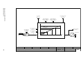
1
MICROMASTER 430
Parameter List
User Documentation
6SE6400-5AF00-0BP0
Issue 08/02
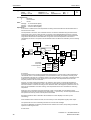
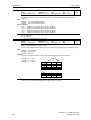
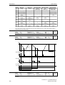
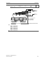
Getting Started Guide
Is for quick commissioning with SDP and BOP-2.
Operating Instructions
Gives information about features of the
MICROMASTER 430, Installation, Commissioning,
Control modes, System Parameter structure,
Troubleshooting, Specifications and available options
of the MICROMASTER 430
Parameter List
The Parameterlist containes the description of all
Parameters structured in functional order and a
detailed description. The Parameter list also includes
a series of function plans.
Catalogues
In the catalogue you will find all needs to select a
certain inverter, as well as filters chokes, operator
panels or communications options.
MICROMASTER 430
Parameter List
User Documentation
Valid for
Converter Type
MICROMASTER 430
Issue 08/02
Issue 08/02
Software V2.0
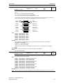
Parameter List
1
Function Diagrams
2
Alarms and
Warnings
3
Parameters
!
Issue 08/02
Warning
Please refer to all Definitiones and Warnings contained in the Operating Instructions. You will find the
Operating Instructions on the Docu CD delivered with your inverter. If the CD is lost, it can be ordered
via your local Siemens department under the Order No. 6SE6400-5AE00-1AP0.
Further information can be obtained from Internet website:
http://www.siemens.de/micromaster
Approved Siemens Quality for Software and Training
is to DIN ISO 9001, Reg. No. 2160-01
The reproduction, transmission or use of this document, or its
contents is not permitted unless authorized in writing.
Offenders will be liable for damages. All rights including rights
created by patent grant or registration of a utility model or
design are reserved.
© Siemens AG 2002. All Rights Reserved.
MICROMASTER® is a registered trademark of Siemens
Other functions not described in this document may be
available. However, this fact shall not constitute an obligation
to supply such functions with a new control, or when
servicing.
We have checked that the contents of this document
correspond to the hardware and software described. There
may be discrepancies nevertheless, and no guarantee can be
given that they are completely identical. The information
contained in this document is reviewed regularly and any
necessary changes will be included in the next edition. We
welcome suggestions for improvement.
Siemens handbooks are printed on chlorine-free paper that
has been produced from managed sustainable forests. No
solvents have been used in the printing or binding process.
Document subject to change without prior notice.
Printed in the Federal of Germany
4
Siemens-Aktiengesellschaft.
MICROMASTER 430 Parameter List
6SE6400-5AF00-0BP0
Issue 08/02
Parameters
Parameters MICROMASTER 430
This Parameter List must only be used together with the Operating Instructions or
the Reference Manual of the MICROMASTER 430. Please pay special attention to
the Warnings, Cautions, Notices and Notes contained in these manuals.
Table of Contents
1
Parameters ............................................................................................... 7
1.1
Introduction to MICROMASTER 430 System Parameters ........................ 7
1.2
Quick commissioning (P0010=1) ............................................................. 10
1.3
Command and Drive Datasets - Overview .............................................. 12
1.4
Binector Input-Parameter......................................................................... 16
1.5
Connector Input-Parameter ..................................................................... 17
1.6
Binector Output-Parameter...................................................................... 17
1.7
Connector Output Parameter................................................................... 18
1.8
Connector/Binector Output-Parameter .................................................... 18
1.9
Parameter Description ............................................................................. 19
2
Function Diagrams .............................................................................. 187
3
Faults and Alarms................................................................................ 217
3.1
Fault messages...................................................................................... 217
3.2
Alarm Messages .................................................................................... 222
MICROMASTER 430 Parameter List
6SE6400-5AF00-0BP0
5
Parameters
6
Issue 08/02
MICROMASTER 430 Parameter List
6SE6400-5AF00-0BP0
Issue 08/02
Parameters
1
Parameters
1.1
Introduction to MICROMASTER 430 System
Parameters
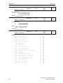
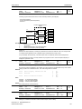
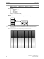
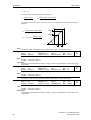
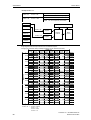
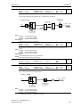
The layout of the parameter description is as follows.
1 Par number 2 Parameter name
[index]
3 CStat:
4 P-Group:
5 Datatype
6 active:
13
7 Unit:
8 Quick Comm:
9 Min:
10 Def:
11 Max:
12 Level:
2
Description:
1. Parameter number
Indicates the relevant parameter number. The numbers used are 4-digit
numbers in the range 0000 to 9999. Numbers prefixed with an “r” indicate that
the parameter is a “read-only” parameter, which displays a particular value but
cannot be changed directly by specifying a different value via this parameter
number (in such cases, dashes “-“ are entered at the points “Unit”, “Min”, “Def”
and “Max” in the header of the parameter description.
All other parameters are prefixed with a “P”. The values of these parameters
can be changed directly in the range indicated by the “Min” and “Max” settings
in the header.
[index] indicates that the parameter is an indexed parameter and specifies the
number of indices available.
2. Parameter name
Indicates the name of the relevant parameter. Certain parameter names
include the following abbreviated prefixes: BI, BO, CI, and CO followed by a
colon.
These abbreviations have the following meanings:
BI
=
P9999.C
(0)
Binector input, i.e. parameter selects the source of a
binary signal
Binector output, i.e. parameter connects as a binary
signal
BO
=
r9999
CI
=
P9999.D
(999:9)
Connector input, i.e. parameter selects the source of
an analog signal
CO
=
r9999 [99]
Connector output, i.e. parameter connects as an
analog signal
r9999
r9999
Connector/Binector output, i.e. parameter connects as
an analog signal and/or as a binary signal
CO/BO =
To make use of BiCo you will need access to the full parameter list. At this
level many new parameter settings are possible, including BiCo functionality.
BiCo functionality is a different, more flexible way of setting and combining
input and output functions. It can be used in most cases in conjunction with the
simple, level 2 settings.
The BiCo system allows complex functions to be programmed. Boolean and
mathematical relationships can be set up between inputs (digital, analog, serial
etc.) and outputs (inverter current, frequency, analog output, relays, etc.).
MICROMASTER 430 Parameter List
6SE6400-5AF00-0BP0
7
Parameters
Issue 08/02
3. CStat
Commissioning status of the parameter. Three states are possible:
Commissioning
C
Run
U
Ready to run
T
This indicates when the parameter can be changed. One, two or all three
states may be specified. If all three states are specified, this means that it is
possible to change this parameter setting in all three inverter states
4. P-Group
Indicates the functional group of the particular.
Note
Parameter P0004 (parameter filter) acts as a filter and focuses access to
parameters according to the functional group selected.
5. Datatype
The data types available are shown in the table below.
Notation
Meaning
U16
16-bit unsigned
U32
32-bit unsigned
I16
16-bit integer
I32
32-bit integer
Float
Floating point
6. Active
Indicates whether
♦ Immediately changes to the parameter values take effective immediately
after they have been entered, or
♦
first confirm
the “P” button on the operator panel (BOP or AOP) must be
pressed before the changes take effect.
7. Unit
Indicates the unit of measure applicable to the parameter values
8. QuickComm
Indicates whether or not (Yes or No) a parameter can only be changed during
quick commissioning, i.e. when P0010 (parameter groups for commissioning)
is set to 1 (quick commissioning).
9. Min
Indicates the minimum value to which the parameter can be set.
10. Def
Indicates the default value, i.e. the value which applies if the user does not
specify a particular value for the parameter.
11. Max
Indicates the maximum value to which the parameter can be set.
12. Level
Indicates the level of user access. There are four access levels: Standard,
Extended, Expert and Service. The number of parameters that appear in each
functional group depends on the access level set in P0003 (user access level).
13. Description
The parameter description consists of the sections and contents listed below.
Some of these sections and contents are optional and will be omitted on a
case-to-case basis if not applicable.
Description:
Brief explanation of the parameter function.
Diagram:
Where applicable, diagram to illustrate the effects of
parameters on a characteristic curve, for example
Settings:
List of applicable settings. These include
Possible settings, Most common settings, Index and Bitfields
Example:
Optional example of the effects of a particular parameter
setting.
8
MICROMASTER 430 Parameter List
6SE6400-5AF00-0BP0
Issue 08/02
Parameters
Dependency:
Any conditions that must be satisfied in connection with this
parameter. Also any particular effects, which this parameter
has on other parameter(s) or which other parameters have
on this one.
Warning / Caution / Notice / Note:
Important information which must be heeded to prevent
personal injury or damage to equipment / specific information
which should be heeded in order to avoid problems /
information which may be helpful to the user
More details:
Any sources of more detailed information concerning the
particular parameter.
MICROMASTER 430 Parameter List
6SE6400-5AF00-0BP0
9
Parameters
1.2
Issue 08/02
Quick commissioning (P0010=1)
The following parameters are necesarry for quick commissioning (P0010=1).
No
Name
P0100
P0205
P0300
P0304
P0305
P0307
P0308
P0309
P0310
P0311
P0320
P0335
P0640
P0700
P1000
P1080
P1082
P1120
P1121
P1135
P1300
P1500
P1910
P3900
Europe / North America
Inverter application
Select motor type
Motor voltage rating
Motor current rating
Motor power rating
Motor cosPhi rating
Motor efficiency rating
Motor frequency rating
Motor speed rating
Motor magnetizing current
Motor cooling
Motor overload factor [%]
Selection of command source
Selection of frequency setpoint
Min. speed
Max. speed
Ramp-up time
Ramp-down time
OFF3 ramp-down time
Control mode
Selection of torque setpoint
Select motor data identification
End of quick commissioning
Access level
1
3
2
1
1
1
2
2
1
1
3
2
2
1
1
1
1
1
1
2
2
2
2
1
Cstat
C
C
C
C
C
C
C
C
C
C
CT
CT
CUT
CT
CT
CUT
CT
CUT
CUT
CUT
CT
CT
CT
C
When P0010=1 is chosen, P0003 (user access level) can be used to select the
parameters to be accessed. This parameter also allows selection of a user-defined
parameter list for quick commissioning.
At the end of the quick commissioning sequence, set P3900 = 1 to carry out the
necessary motor calculations and clear all other parameters (not included in
P0010=1) to their default settings.
Note
This applies only in Quick Commissioning mode.
Reset to Factory default
To reset all parameters to the factory default settings; the following parameters
should be set as follows:
Set P0010 = 30
Set P0970 = 1
Note
The reset process takes approximately 10 seconds to complete. Reset to Factory
default
10
MICROMASTER 430 Parameter List
6SE6400-5AF00-0BP0
Issue 08/02
Parameters
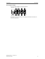
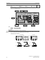
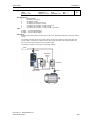
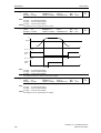
Seven-segment display
The seven-segment display is structured as follows:
Segment Bit
Segment Bit
15 14
7
6
13 12
5
4
11
10
3
2
9
1
8
0
The significance of the relevant bits in the display is described in the status and
control word parameters.
MICROMASTER 430 Parameter List
6SE6400-5AF00-0BP0
11
Parameters
1.3
Issue 08/02
Command and Drive Datasets - Overview
Command Datasets (CDS)
12
ParNr
Parameter name
ParNr
Parameter name
P0700[3]
Selection of command source
P1076[3]
CI: Additional setpoint scaling
P0701[3]
Function of digital input 1
P1110[3]
BI: Inhibit neg. freq. setpoint
P0702[3]
Function of digital input 2
P1113[3]
BI: Reverse
P0703[3]
Function of digital input 3
P1124[3]
BI: Enable JOG ramp times
P0704[3]
Function of digital input 4
P1140[3]
BI: RFG enable
P0705[3]
Function of digital input 5
P1141[3]
BI: RFG start
P0706[3]
Function of digital input 6
P1142[3]
BI: RFG enable setpoint
P0707[3]
Function of digital input 7
P1230[3]
BI: Enable DC braking
P0708[3]
Function of digital input 8
P1266[3]
BI: Bypass command
P0719[3]
Selection of cmd. & freq. setp.
P1270[3]
BI: Enable essential service
P0731[3]
BI: Function of digital output 1
P1330[3]
CI: Voltage setpoint
P0732[3]
BI: Function of digital output 2
P1477[3]
BI: Set integrator of n-ctrl.
P0733[3]
BI: Function of digital output 3
P1478[3]
CI: Set integrator value n-ctrl.
P0800[3]
BI: Download parameter set 0
P1500[3]
Selection of torque setpoint
P0801[3]
BI: Download parameter set 1
P1501[3]
BI: Change to torque control
P0840[3]
BI: ON/OFF1
P1503[3]
CI: Torque setpoint
P0842[3]
BI: ON reverse/OFF1
P1511[3]
CI: Additional torque setpoint
P0844[3]
BI: 1. OFF2
P1522[3]
CI: Upper torque limit
P0845[3]
BI: 2. OFF2
P1523[3]
CI: Lower torque limit
P0848[3]
BI: 1. OFF3
P2103[3]
BI: 1. Faults acknowledgement
P0849[3]
BI: 2. OFF3
P2104[3]
BI: 2. Faults acknowledgement
P0852[3]
BI: Pulse enable
P2106[3]
BI: External fault
P1000[3]
Selection of frequency setpoint
P2151[3]
CI: Monitoring speed setpoint
P1020[3]
BI: Fixed freq. selection Bit 0
P2152[3]
CI: Act. monitoring speed
P1021[3]
BI: Fixed freq. selection Bit 1
P2200[3]
BI: Enable PID controller
P1022[3]
BI: Fixed freq. selection Bit 2
P2220[3]
BI: Fixed PID setp. select Bit 0
P1023[3]
BI: Fixed freq. selection Bit 3
P2221[3]
BI: Fixed PID setp. select Bit 1
P1026[3]
BI: Fixed freq. selection Bit 4
P2222[3]
BI: Fixed PID setp. select Bit 2
P1028[3]
BI: Fixed freq. selection Bit 5
P2223[3]
BI: Fixed PID setp. select Bit 3
P1035[3]
BI: Enable MOP (UP-command)
P2226[3]
BI: Fixed PID setp. select Bit 4
P1036[3]
BI: Enable MOP (DOWN-command)
P2228[3]
BI: Fixed PID setp. select Bit 5
P1055[3]
BI: Enable JOG right
P2235[3]
BI: Enable PID-MOP (UP-cmd)
P1056[3]
BI: Enable JOG left
P2236[3]
BI: Enable PID-MOP (DOWN-cmd)
P1070[3]
CI: Main setpoint
P2253[3]
CI: PID setpoint
P1071[3]
CI: Main setpoint scaling
P2254[3]
CI: PID trim source
P1074[3]
BI: Disable additional setpoint
P2264[3]
CI: PID feedback
P1075[3]
CI: Additional setpoint
MICROMASTER 430 Parameter List
6SE6400-5AF00-0BP0
Issue 08/02
Parameters
Drive Datasets (DDS)
ParNr
Parameter name
ParNr
P0005[3]
Display selection
r0374[3]
Rotor resistance [%]
r0035[3]
CO: Act. motor temperature
r0376[3]
Rated rotor resistance [%]
P0291[3]
Inverter protection
r0377[3]
Total leakage reactance [%]
P0300[3]
Select motor type
r0382[3]
Main reactance [%]
P0304[3]
Rated motor voltage
r0384[3]
Rotor time constant
P0305[3]
Rated motor current
r0386[3]
Total leakage time constant
P0307[3]
Rated motor power
P0400[3]
Select encoder type
P0308[3]
Rated motor cosPhi
P0408[3]
Encoder pulses per revolution
P0309[3]
Rated motor efficiency
P0491[3]
Reaction on speed signal loss
P0310[3]
Rated motor frequency
P0492[3]
Allowed speed difference
P0311[3]
Rated motor speed
P0494[3]
Delay speed loss reaction
r0313[3]
Motor pole pairs
P0500[3]
Technological application
P0314[3]
Motor pole pair number
P0601[3]
Motor temperature sensor
P0320[3]
Motor magnetizing current
P0604[3]
Threshold motor temperature
r0330[3]
Rated motor slip
P0625[3]
Ambient motor temperature
r0331[3]
Rated magnetization current
P0626[3]
Overtemperature stator iron
r0332[3]
Rated power factor
P0627[3]
Overtemperature stator winding
r0333[3]
Rated motor torque
P0628[3]
Overtemperature rotor winding
P0335[3]
Motor cooling
r0630[3]
CO: Ambient temperature
P0340[3]
Calculation of motor parameters
r0631[3]
CO: Stator iron temperature
P0341[3]
Motor inertia [kg*m^2]
r0632[3]
CO: Stator winding temperature
P0342[3]
Total/motor inertia ratio
r0633[3]
CO: Rotor winding temperature
P0344[3]
Motor weight
P0640[3]
Motor overload factor [%]
r0345[3]
Motor start-up time
P1001[3]
Fixed frequency 1
P0346[3]
Magnetization time
P1002[3]
Fixed frequency 2
P0347[3]
Demagnetization time
P1003[3]
Fixed frequency 3
P0350[3]
Stator resistance (line-to-line)
P1004[3]
Fixed frequency 4
P0352[3]
Cable resistance
P1005[3]
Fixed frequency 5
P0354[3]
Rotor resistance
P1006[3]
Fixed frequency 6
P0356[3]
Stator leakage inductance
P1007[3]
Fixed frequency 7
P0358[3]
Rotor leakage inductance
P1008[3]
Fixed frequency 8
P0360[3]
Main inductance
P1009[3]
Fixed frequency 9
P0362[3]
Magnetizing curve flux 1
P1010[3]
Fixed frequency 10
P0363[3]
Magnetizing curve flux 2
P1011[3]
Fixed frequency 11
P0364[3]
Magnetizing curve flux 3
P1012[3]
Fixed frequency 12
P0365[3]
Magnetizing curve flux 4
P1013[3]
Fixed frequency 13
P0366[3]
Magnetizing curve imag 1
P1014[3]
Fixed frequency 14
P0367[3]
Magnetizing curve imag 2
P1015[3]
Fixed frequency 15
P0368[3]
Magnetizing curve imag 3
P1031[3]
Setpoint memory of the MOP
P0369[3]
Magnetizing curve imag 4
P1040[3]
Setpoint of the MOP
r0370[3]
Stator resistance [%]
P1058[3]
JOG frequency right
r0372[3]
Cable resistance [%]
P1059[3]
JOG frequency left
r0373[3]
Rated stator resistance [%]
P1060[3]
JOG ramp-up time
MICROMASTER 430 Parameter List
6SE6400-5AF00-0BP0
Parameter name
13
Parameters
14
Issue 08/02
ParNr
Parameter name
ParNr
Parameter name
P1061[3]
JOG ramp-down time
P1346[3]
Imax voltage ctrl. integral time
P1080[3]
Min. frequency
P1350[3]
Voltage soft start
P1082[3]
Max. frequency
P1400[3]
Configuration of speed control
P1091[3]
Skip frequency 1
P1442[3]
Filter time for act. speed
P1092[3]
Skip frequency 2
P1452[3]
Filter time for act.speed (SLVC)
P1093[3]
Skip frequency 3
P1460[3]
Gain speed controller
P1094[3]
Skip frequency 4
P1462[3]
Integral time speed controller
P1101[3]
Skip frequency bandwidth
P1470[3]
Gain speed controller (SLVC)
P1120[3]
Ramp-up time
P1472[3]
Integral time n-ctrl. (SLVC)
P1121[3]
Ramp-down time
P1488[3]
Droop input source
P1130[3]
Ramp-up initial rounding time
P1489[3]
Droop scaling
P1131[3]
Ramp-up final rounding time
P1492[3]
Enable droop
P1132[3]
Ramp-down initial rounding time
P1496[3]
Scaling accel. precontrol
P1133[3]
Ramp-down final rounding time
P1499[3]
Scaling accel. torque control
P1134[3]
Rounding type
P1520[3]
CO: Upper torque limit
P1135[3]
OFF3 ramp-down time
P1521[3]
CO: Lower torque limit
P1202[3]
Motor-current: Flying start
P1525[3]
Scaling lower torque limit
P1203[3]
Search rate: Flying start
P1530[3]
Motoring power limitation
P1232[3]
DC braking current
P1531[3]
Regenerative power limitation
P1233[3]
Duration of DC braking
P1654[3]
Smooth time for Isq setpoint
P1234[3]
DC braking start frequency
P1715[3]
Gain current controller
P1236[3]
Compound braking current
P1717[3]
Integral time current controller
P1240[3]
Configuration of Vdc controller
P1803[3]
Max. modulation
P1243[3]
Dynamic factor of Vdc-max
P1820[3]
Reverse output phase sequence
P1250[3]
Gain of Vdc-controller
P2000[3]
Reference frequency
P1251[3]
Integration time Vdc-controller
P2001[3]
Reference voltage
P1252[3]
Differential time Vdc-controller
P2002[3]
Reference current
P1253[3]
Vdc-controller output limitation
P2003[3]
Reference torque
P1260[3]
Bypass control
r2004[3]
Reference power
P1262[3]
Bypass dead time
P2150[3]
Hysteresis frequency f_hys
P1263[3]
De-Bypass time
P2153[3]
Time-constant speed filter
P1264[3]
Bypass time
P2155[3]
Threshold frequency f_1
P1265[3]
Bypass frequency
P2156[3]
Delay time of threshold freq f_1
P1300[3]
Control mode
P2157[3]
Threshold frequency f_2
P1310[3]
Continuous boost
P2158[3]
Delay time of threshold freq f_2
P1311[3]
Acceleration boost
P2159[3]
Threshold frequency f_3
P1312[3]
Starting boost
P2160[3]
Delay time of threshold freq f_3
P1316[3]
Boost end frequency
P2161[3]
Min. threshold for freq. setp.
P1320[3]
Programmable V/f freq. coord. 1
P2162[3]
Hysteresis freq. for overspeed
P1321[3]
Programmable V/f volt. coord. 1
P2163[3]
Entry freq. for perm. deviation
P1322[3]
Programmable V/f freq. coord. 2
P2164[3]
Hysteresis frequency deviation
P1323[3]
Programmable V/f volt. coord. 2
P2165[3]
Delay time permitted deviation
P1324[3]
Programmable V/f freq. coord. 3
P2166[3]
Delay time ramp up completed
P1325[3]
Programmable V/f volt. coord. 3
P2167[3]
Switch-off frequency f_off
P1333[3]
Start frequency for FCC
P2168[3]
Delay time T_off
P1335[3]
Slip compensation
P2170[3]
Threshold current I_thresh
P1336[3]
Slip limit
P2171[3]
Delay time current
P1338[3]
Resonance damping gain V/f
P2172[3]
Threshold DC-link voltage
P1340[3]
Imax freq. controller prop. gain
P2173[3]
Delay time DC-link voltage
P1341[3]
Imax freq. ctrl. integral time
P2174[3]
Torque threshold M_thresh
P1345[3]
Imax voltage ctrl. prop. gain
P2176[3]
Delay time for torque threshold
MICROMASTER 430 Parameter List
6SE6400-5AF00-0BP0
Issue 08/02
Parameters
ParNr
Parameter name
ParNr
Parameter name
P2177[3]
Delay time for motor is blocked
P2208[3]
Fixed PID setpoint 8
P2178[3]
Delay time for motor pulled out
P2209[3]
Fixed PID setpoint 9
P2181[3]
Belt failure detection mode
P2210[3]
Fixed PID setpoint 10
P2182[3]
Belt threshold frequency 1
P2211[3]
Fixed PID setpoint 11
P2183[3]
Belt threshold frequency 2
P2212[3]
Fixed PID setpoint 12
P2184[3]
Belt threshold frequency 3
P2213[3]
Fixed PID setpoint 13
P2185[3]
Upper torque threshold 1
P2214[3]
Fixed PID setpoint 14
P2186[3]
Lower torque threshold 1
P2215[3]
Fixed PID setpoint 15
P2187[3]
Upper torque threshold 2
P2231[3]
Setpoint memory of PID-MOP
P2188[3]
Lower torque threshold 2
P2240[3]
Setpoint of PID-MOP
P2189[3]
Upper torque threshold 3
P2370[3]
Motor staging stop mode
P2190[3]
Lower torque threshold 3
P2371[3]
Motor staging configuration
P2192[3]
Time delay for belt failure
P2372[3]
Motor staging cycling
P2201[3]
Fixed PID setpoint 1
P2373[3]
Motor staging hysteresis
P2202[3]
Fixed PID setpoint 2
P2374[3]
Motor staging delay
P2203[3]
Fixed PID setpoint 3
P2375[3]
Motor destaging delay
P2204[3]
Fixed PID setpoint 4
P2376[3]
Motor staging delay override
P2205[3]
Fixed PID setpoint 5
P2377[3]
Motor staging lockout timer
P2206[3]
Fixed PID setpoint 6
P2378[3]
Motor staging frequency f_st [%]
P2207[3]
Fixed PID setpoint 7
MICROMASTER 430 Parameter List
6SE6400-5AF00-0BP0
15
Parameters
1.4
16
Issue 08/02
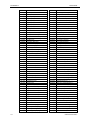
Binector Input-Parameter
P-Nr.
Parametername
P-Nr.
Parametername
P0731[3]
BI: Function of digital output 1
P2104[3]
BI: 2. Faults acknowledgement
P0732[3]
BI: Function of digital output 2
P2106[3]
BI: External fault
P0733[3]
BI: Function of digital output 3
P2200[3]
BI: Enable PID controller
P0800[3]
BI: Download parameter set 0
P2220[3]
BI: Fixed PID setp. select Bit 0
P0801[3]
BI: Download parameter set 1
P2221[3]
BI: Fixed PID setp. select Bit 1
P0810
BI: CDS bit 0 (Local / Remote)
P2222[3]
BI: Fixed PID setp. select Bit 2
P0811
BI: CDS bit 1
P2223[3]
BI: Fixed PID setp. select Bit 3
P0820
BI: DDS bit 0
P2226[3]
BI: Fixed PID setp. select Bit 4
P0821
BI: DDS bit 1
P2228[3]
BI: Fixed PID setp. select Bit 5
P0840[3]
BI: ON/OFF1
P2235[3]
BI: Enable PID-MOP (UP-cmd)
P0842[3]
BI: ON reverse/OFF1
P2236[3]
BI: Enable PID-MOP (DOWN-cmd)
P0844[3]
BI: 1. OFF2
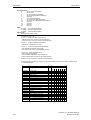
P2810[2]
BI: AND 1
P0845[3]
BI: 2. OFF2
P2812[2]
BI: AND 2
P0848[3]
BI: 1. OFF3
P2814[2]
BI: AND 3
P0849[3]
BI: 2. OFF3
P2816[2]
BI: OR 1
P0852[3]
BI: Pulse enable
P2818[2]
BI: OR 2
P1020[3]
BI: Fixed freq. selection Bit 0
P2820[2]
BI: OR 3
P1021[3]
BI: Fixed freq. selection Bit 1
P2822[2]
BI: XOR 1
P1022[3]
BI: Fixed freq. selection Bit 2
P2824[2]
BI: XOR 2
P1023[3]
BI: Fixed freq. selection Bit 3
P2826[2]
BI: XOR 3
P1026[3]
BI: Fixed freq. selection Bit 4
P2828
BI: NOT 1
P1028[3]
BI: Fixed freq. selection Bit 5
P2830
BI: NOT 2
P1035[3]
BI: Enable MOP (UP-command)
P2832
BI: NOT 3
P1036[3]
BI: Enable MOP (DOWN-command)
P2834[4]
BI: D-FF 1
P1074[3]
BI: Disable additional setpoint
P2837[4]
BI: D-FF 2
P1110[3]
BI: Inhibit neg. freq. setpoint
P2840[2]
BI: RS-FF 1
P1113[3]
BI: Reverse
P2843[2]
BI: RS-FF 2
P1140[3]
BI: RFG enable
P2846[2]
BI: RS-FF 3
P1141[3]
BI: RFG start
P2849
BI: Timer 1
P1142[3]
BI: RFG enable setpoint
P2854
BI: Timer 2
P1230[3]
BI: Enable DC braking
P2859
BI: Timer 3
P1266[3]
BI: Bypass command
P2864
BI: Timer 4
P2103[3]
BI: 1. Faults acknowledgement
MICROMASTER 430 Parameter List
6SE6400-5AF00-0BP0
Issue 08/02
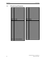
1.5
Parameters
Connector Input-Parameter
P-Nr.
1.6
Parametername
P-Nr.
Parametername
P0095[10] CI: Display PZD signals
P2264[3]
CI: PID feedback
P0771[2]
CI: DAC
P2869[2]
CI: ADD 1
P1070[3]
CI: Main setpoint
P2871[2]
CI: ADD 2
P1071[3]
CI: Main setpoint scaling
P2873[2]
CI: SUB 1
P1075[3]
CI: Additional setpoint
P2875[2]
CI: SUB 2
P1076[3]
CI: Additional setpoint scaling
P2877[2]
CI: MUL 1
P1330[3]
CI: Voltage setpoint
P2879[2]
CI: MUL 2
P2016[8]
CI: PZD to BOP link (USS)
P2881[2]
CI: DIV 1
P2019[8]
CI: PZD to COM link (USS)
P2883[2]
CI: DIV 2
P2051[8]
CI: PZD to CB
P2885[2]
CI: CMP 1
P2253[3]
CI: PID setpoint
P2887[2]
CI: CMP 2
P2254[3]
CI: PID trim source
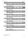
Binector Output-Parameter
P-Nr.
Parametername
P-Nr.
Parametername
r1261
BO: Bypass status word
r2836
BO: NOT-Q D-FF 1
r2032
BO: CtrlWrd1 from BOP link (USS)
r2838
BO: Q D-FF 2
r2033
BO: CtrlWrd2 from BOP link (USS)
r2839
BO: NOT-Q D-FF 2
r2036
BO: CtrlWrd1 from COM link (USS)
r2841
BO: Q RS-FF 1
r2037
BO: CtrlWrd2 from COM link (USS)
r2842
BO: NOT-Q RS-FF 1
r2090
BO: Control word 1 from CB
r2844
BO: Q RS-FF 2
r2091
BO: Control word 2 from CB
r2845
BO: NOT-Q RS-FF 2
r2811
BO: AND 1
r2847
BO: Q RS-FF 3
r2813
BO: AND 2
r2848
BO: NOT-Q RS-FF 3
r2815
BO: AND 3
r2852
BO: Timer 1
r2817
BO: OR 1
r2853
BO: Nout timer 1
r2819
BO: OR 2
r2857
BO: Timer 2
r2821
BO: OR 3
r2858
BO: Nout timer 2
r2823
BO: XOR 1
r2862
BO: Timer 3
r2825
BO: XOR 2
r2863
BO: Nout timer 3
r2827
BO: XOR 3
r2867
BO: Timer 4
r2829
BO: NOT 1
r2868
BO: Nout timer 4
r2831
BO: NOT 2
r2886
BO: CMP 1
r2833
BO: NOT 3
r2888
BO: CMP 2
r2835
BO: Q D-FF 1
MICROMASTER 430 Parameter List
6SE6400-5AF00-0BP0
17
Parameters
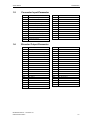
1.7
Issue 08/02
Connector Output Parameter
P-Nr.
1.8
18
Parametername
P-Nr.
Parametername
r0020
CO: Freq. setpoint before RFG
r1170
CO: Frequency setpoint after RFG
r0021
CO: Act. filtered frequency
r1242
CO: Switch-on level of Vdc-max
r0024
CO: Act. filtered output freq.
r1337
CO: V/f slip frequency
r0025
CO: Act. filtered output voltage
r1343
CO: Imax controller freq. output
r0026
CO: Act. filtered DC-link volt.
r1344
CO: Imax controller volt. output
r0027
CO: Act. filtered output current
r1801
CO: Act. pulse frequency
r0031
CO: Act. filtered torque
r2015[8]
CO: PZD from BOP link (USS)
r0032
CO: Act. filtered power
r2018[8]
CO: PZD from COM link (USS)
r0035[3]
CO: Act. motor temperature
r2050[8]
CO: PZD from CB
r0037[5]
CO: Inverter temperature [°C]
r2169
CO: Act. filtered frequency
r0038
CO: Act. power factor
r2224
CO: Act. fixed PID setpoint
r0039
CO: Energy consumpt. meter [kWh]
r2250
CO: Output setpoint of PID-MOP
r0050
CO: Active command data set
r2260
CO: PID setpoint after PID-RFG
r0051[2]
CO: Active drive data set (DDS)
r2262
CO: Filtered PID setp. after RFG
r0061
CO: Act. rotor speed
r2266
CO: PID filtered feedback
r0063
CO: Act. frequency
r2272
CO: PID scaled feedback
r0065
CO: Slip frequency
r2273
CO: PID error
r0067
CO: Act. output current limit
r2294
CO: Act. PID output
r0071
CO: Max. output voltage
r2870
CO: ADD 1
r0080
CO: Act. torque
r2872
CO: ADD 2
r0086
CO: Act. active current
r2874
CO: SUB 1
r0395
CO: Total stator resistance [%]
r2876
CO: SUB 2
r0396
CO: Act. rotor resistance
r2878
CO: MUL 1
r0755[2]
CO: Act. ADC after scal. [4000h]
r2880
CO: MUL 2
r1024
CO: Act. fixed frequency
r2882
CO: DIV 1
r1050
CO: Act. Output freq. of the MOP
r2884
CO: DIV 2
r1078
CO: Total frequency setpoint
P2889
CO: Fixed setpoint 1 in [%]
r1114
CO: Freq. setp. after dir. ctrl.
P2890
CO: Fixed setpoint 2 in [%]
r1119
CO: Freq. setpoint before RFG
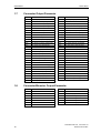
Connector/Binector Output-Parameter
P-Nr.
Parametername
P-Nr.
Parametername
r0019
CO/BO: BOP control word
P0718
CO/BO: Hand / Auto
r0052
CO/BO: Act. status word 1
r0722
CO/BO: Binary input values
r0053
CO/BO: Act. status word 2
r0747
CO/BO: State of digital outputs
r0054
CO/BO: Act. control word 1
r2197
CO/BO: Monitoring word 1
r0055
CO/BO: Act. control word 2
r2198
CO/BO: Monitoring word 2
r0056
CO/BO: Status of motor control
r2379
CO/BO: Motor staging status word
r0403
CO/BO: Encoder status word
MICROMASTER 430 Parameter List
6SE6400-5AF00-0BP0
Issue 08/02
1.9
Parameters
Parameter Description
Note:
Level 4 Parameters are not visible with BOP or AOP.
r0000
Drive display
Datatype: U16
Unit: -
P-Group: ALWAYS
Min:
Def:
Max:
-
Level:
1
Displays the user selected output as defined in P0005.
Note:
Pressing the "Fn" button for 2 seconds allows the user to view the values of DC link voltage, output
frequency, output voltage, output current, and chosen r0000 setting (defined in P0005).
r0002
Drive state
Datatype: U16
P-Group: COMMANDS
Unit: -
Min:
Def:
Max:
-
Level:
3
Displays actual drive state.
Possible Settings:
0
Commissioning mode (P0010 != 0)
1
Drive ready
2
Drive fault active
3
Drive starting (DC-link precharging)
4
Drive running
5
Stopping (ramping down)
Dependency:
State 3 visible only while precharging DC link, and when externally powered communications board is fitted.
Level:
P0003
User access level
Min: 0
CStat:
CUT
Datatype: U16
Unit: Def:
1
P-Group: ALWAYS
Active: first confirm
QuickComm. No
Max: 4
1
Defines user access level to parameter sets. The default setting (standard) is sufficient for most simple
applications.
Possible Settings:
0
User defined parameter list - see P0013 for details on use
1
Standard: Allows access into most frequently used parameters.
2
Extended: Allows extended access e.g. to inverter I/O functions.
3
Expert: For expert use only.
4
Service: Only for use by authorized service personal - password protected.
Level:
P0004
Parameter filter
Min: 0
CStat:
CUT
Datatype: U16
Unit: Def:
0
P-Group: ALWAYS
Active: first confirm
QuickComm. No
Max: 22
1
Filters available parameters according to functionality to enable a more focussed approach to
commissioning.
Possible Settings:
0
All parameters
2
Inverter
3
Motor
4
Speed sensor
5
Technol. application / units
7
Commands, binary I/O
8
ADC and DAC
10
Setpoint channel / RFG
12
Drive features
13
Motor control
20
Communication
21
Alarms / warnings / monitoring
22
Technology controller (e.g. PID)
Example:
P0004 = 22 specifies that only PID parameters will be visible.
Dependency:
Parameters marked "Quick Comm: Yes" in the parameter header can only be set when P0010 = 1 (Quick
Commissioning).
Parameter List MICROMASTER 430
6SE6400-5AF00-0BP0
19
Parameters
P0005[3]
Issue 08/02
Display selection
CStat:
CUT
P-Group: FUNC
Datatype: U16
Active: first confirm
Unit: QuickComm. No
Min:
Def:
Max:
2
21
4000
Level:
Min:
Def:
Max:
0
2
4
Level:
2
Selects display for parameter r0000 (drive display).
Index:
P0005[0] : 1st. Drive data set (DDS)
P0005[1] : 2nd. Drive data set (DDS)
P0005[2] : 3rd. Drive data set (DDS)
Common Settings:
21 Actual frequency
25 Output voltage
26 DC link voltage
27 Output current
Notice:
These settings refer to read only parameter numbers ("rxxxx").
Details:
See relevant "rxxxx" parameter descriptions.
P0006
Display mode
CStat:
CUT
P-Group: FUNC
Datatype: U16
Active: first confirm
Unit: QuickComm. No
3
Defines mode of display for r0000 (drive display).
Possible Settings:
0
In Ready state alternate between setpoint and output frequency. In run display output frequency
1
In Ready state display setpoint. In run display output frequency.
2
In Ready state alternate between P0005 value and r0020 value. In run display P0005 value
3
In Ready state alternate between r0002 value and r0020 value. In run display r0002 value
4
In all states just display P0005
Note:
When inverter is not running, the display alternates between the values for "Not Running" and "Running".
Per default, the setpoint and actual frequency values are displayed alternately.
P0007
Backlight delay time
CStat:
CUT
P-Group: FUNC
Datatype: U16
Active: first confirm
Unit: QuickComm. No
Min:
Def:
Max:
0
0
2000
Level:
3
Defines time period after which the backlight display turns off if no operator keys have been pressed.
Value:
P0007 = 0:
Backlight always on (default state).
P0007 = 1 - 2000:
Number of seconds after which the backlight will turn off.
P0010
Commissioning parameter
CStat:
CT
P-Group: ALWAYS
Datatype: U16
Active: first confirm
Unit: QuickComm. No
Min:
Def:
Max:
0
0
30
Level:
1
Filters parameters so that only those related to a particular functional group are selected.
Possible Settings:
0
Ready
1
Quick commissioning
2
Inverter
29
Download
30
Factory setting
Dependency:
Reset to 0 for inverter to run.
P0003 (user access level) also determines access to parameters.
Parameter List
20
MICROMASTER 430
6SE6400-5AF00-0BP0
Issue 08/02
Parameters
Note:
P0010 = 1
The inverter can be commissioned very quickly and easily by setting P0010 = 1. After that only the important
parameters (e.g.: P0304, P0305, etc.) are visible. The value of these parameters must be entered one after
the other. The end of quick commissioning and the start of internal calculation will be done by setting P3900
= 1 - 3. Afterward parameter P0010 will be reset to zero automatically.
P0010 = 2
For service purposes only.
P0010 = 29
To transfer a parameter file via PC tool (e.g.: DriveMonitor, STARTER) parameter P0010 will be set to 29 by
the PC tool. When download has been finished PC tool resets parameter P0010 to zero.
P0010 = 30
When resetting the parameters of inverter P0010 must be set to 30. Resetting of the parameters will be
started by setting parameter P0970 = 1. The inverter will automatically reset all its parameters to their
default settings. This can prove beneficial if you experience problems during parameter setup and wish to
start again. Duration of factory setting will take about 60 s.
If P3900 is not 0 (0 is the default value), this parameter is automatically reset to 0.
P0011
Min:
Def:
Max:
0
0
65535
Level:
Unit: QuickComm. No
Min:
Def:
Max:
0
0
65535
Level:
Unit: QuickComm. No
Min:
Def:
Max:
0
0
65535
Level:
Unit: QuickComm. No
Lock for user defined parameter
CStat:
CUT
P-Group: FUNC
Datatype: U16
Active: first confirm
3
Details:
See parameter P0013 (user defined parameter)
P0012
Key for user defined parameter
CStat:
CUT
P-Group: FUNC
Datatype: U16
Active: first confirm
3
Details:
See parameter P0013 (user defined parameter).
P0013[20]
User defined parameter
CStat:
CUT
P-Group: FUNC
Datatype: U16
Active: first confirm
3
Defines a limited set of parameters to which the end user will have access.
Instructions for use:
Step 1: Set P0003 = 3 (expert user)
Step 2: Go to P0013 indices 0 to 16 (user list)
Step 3: Enter into P0013 index 0 to 16 the parameters required to be visible in the user-defined list.
The following values are fixed and cannot be changed:
- P0013 index 19 = 12 (key for user defined parameter)
- P0013 index 18 = 10 (commissioning parameter filter)
- P0013 index 17 = 3 (user access level)
Step 4: Set P0003 = 0 to activate the user defined parameter.
Index:
P0013[0] : 1st user parameter
P0013[1] : 2nd user parameter
P0013[2] : 3rd user parameter
P0013[3] : 4th user parameter
P0013[4] : 5th user parameter
P0013[5] : 6th user parameter
P0013[6] : 7th user parameter
P0013[7] : 8th user parameter
P0013[8] : 9th user parameter
P0013[9] : 10th user parameter
P0013[10] : 11th user parameter
P0013[11] : 12th user parameter
P0013[12] : 13th user parameter
P0013[13] : 14th user parameter
P0013[14] : 15th user parameter
P0013[15] : 16th user parameter
P0013[16] : 17th user parameter
P0013[17] : 18th user parameter
P0013[18] : 19th user parameter
P0013[19] : 20th user parameter
Dependency:
First, set P0011 ("lock") to a different value than P0012 ("key") to prevent changes to user-defined
parameter. Then, set P0003 to 0 to activate the user-defined list.
When locked and the user-defined parameter is activated, the only way to exit the user-defined parameter
(and view other parameters) is to set P0012 ("key") to the value in P0011 ("lock").
Parameter List MICROMASTER 430
6SE6400-5AF00-0BP0
21
Parameters
Issue 08/02
Note:
Alternatively, set P0010 = 30 (commissioning parameter filter = factory setting) and P0970 = 1 (factory
reset) to perform a complete factory reset.
The default values of P0011 ("lock") and P0012 ("key") are the same.
r0018
Min:
Def:
Max:
-
Level:
Unit: -
Min:
Def:
Max:
-
Level:
Unit: -
Firmware version
Datatype: Float
P-Group: INVERTER
3
Displays version number of installed firmware.
r0019
CO/BO: BOP control word
Datatype: U16
P-Group: COMMANDS
3
Displays status of operator panel commands.
The settings below are used as the "source" codes for keypad control when connecting to BICO input
parameters.
Bitfields:
Bit00
ON/OFF1
0
NO
1
YES
Bit01
OFF2: Electrical stop
0
YES
1
NO
Bit08
JOG right
0
NO
1
YES
Bit11
Reverse (setpoint inversion)
0
NO
1
YES
Bit12
Hand Operation
0
NO
1
YES
Bit13
Motor potentiometer MOP up
0
NO
1
YES
Bit14
Motor potentiometer MOP down
0
NO
1
YES
Bit15
Auto Operation
0
NO
1
YES
Note:
When BICO technology is used to allocate functions to panel buttons, this parameter displays the actual
status of the relevant command.
The following functions can be "connected" to individual buttons:
- ON/OFF1,
- OFF2,
- JOG,
- REVERSE,
- INCREASE,
- DECREASE
r0020
CO: Freq. setpoint before RFG
Datatype: Float
Unit: Hz
P-Group: CONTROL
Min:
Def:
Max:
-
Level:
Min:
Def:
Max:
-
Level:
3
Displays actual frequency setpoint (output from ramp function generator).
r0021
CO: Act. filtered frequency
Datatype: Float
Unit: Hz
P-Group: CONTROL
3
Displays actual inverter output frequency (r0024) excluding slip compensation, resonance damping and
frequency limitation.
Level:
Act. filtered rotor speed
Min: Datatype: Float
Unit: 1/min
Def:
P-Group: CONTROL
Max: -
r0022
3
Displays calculated rotor speed based on inverter output frequency [Hz] x 120 / number of poles.
Note:
This calculation makes no allowance for load-dependent slip.
r0024
CO: Act. filtered output freq.
Datatype: Float
P-Group: CONTROL
r0025
Unit: Hz
Min:
Def:
Max:
-
Level:
3
Displays actual output frequency (slip compensation, resonance damping and frequency limitation are
included).
Level:
CO: Act. filtered output voltage
Min: Datatype: Float
Unit: V
Def:
P-Group: CONTROL
Max: -
3
Displays [rms] voltage applied to motor.
Parameter List
22
MICROMASTER 430
6SE6400-5AF00-0BP0
Issue 08/02
r0026
Parameters
Min:
Def:
Max:
-
Level:
Unit: V
Min:
Def:
Max:
-
Level:
Unit: A
Unit: Nm
Min:
Def:
Max:
-
Level:
Datatype: Float
Unit: -
Min:
Def:
Max:
-
Level:
Datatype: Float
CO: Act. filtered DC-link volt.
Datatype: Float
P-Group: INVERTER
3
Displays DC-link voltage.
r0027
CO: Act. filtered output current
Datatype: Float
P-Group: CONTROL
3
Displays [rms] value of motor current [A].
r0031
CO: Act. filtered torque
P-Group: CONTROL
3
Displays motor torque.
r0032
CO: Act. filtered power
P-Group: CONTROL
3
Displays motor power.
Dependency:
Value is displayed in [kW] or [hp] depending on setting for P0100 (operation for Europe / North America).
Level:
r0035[3]
CO: Act. motor temperature
Min: Datatype: Float
Unit: °C
Def:
P-Group: MOTOR
Max: -
3
Displays measured motor temperature.
Index:
r0035[0] : 1st. Drive data set (DDS)
r0035[1] : 2nd. Drive data set (DDS)
r0035[2] : 3rd. Drive data set (DDS)
r0037[5]
CO: Inverter temperature [°C]
Datatype: Float
Unit: °C
P-Group: INVERTER
Min:
Def:
Max:
-
Level:
3
Displays measured heatsink temperature and calculated junction temperature of IGBTs based on thermal
model.
Index:
r0037[0]
r0037[1]
r0037[2]
r0037[3]
r0037[4]
r0038
:
:
:
:
:
Measured heat sink temperature
Chip temperature
Rectifier temperature
Inverter ambient temperature
Control board temperature
CO: Act. power factor
Datatype: Float
Unit: -
P-Group: CONTROL
Min:
Def:
Max:
-
Level:
3
Displays actual power factor.
Dependency:
Applies when V/f control is selected in P1300 (control mode); otherwise, the display shows the value zero.
Level:
r0039
CO: Energy consumpt. meter [kWh]
Min: Datatype: Float
Unit: kWh
Def:
P-Group: INVERTER
Max: -
3
Displays electrical energy used by inverter since display was last reset (see P0040 - reset energy
consumption meter).
Dependency:
Value is reset when
P0040 = 1 reset energy consumption meter.
P0040
Reset energy consumption meter
CStat:
CT
P-Group: INVERTER
Datatype: U16
Active: first confirm
Unit: QuickComm. No
Min:
Def:
Max:
0
0
1
Level:
3
Resets value of parameter r0039 (energy consumption meter) to zero.
Possible Settings:
0
No reset
1
Reset r0039 to 0
Dependency:
No reset until "P" is pressed.
Parameter List MICROMASTER 430
6SE6400-5AF00-0BP0
23
Parameters
r0050
Issue 08/02
CO: Active command data set
Datatype: U16
Unit: -
P-Group: COMMANDS
Min:
Def:
Max:
-
Level:
Min:
Def:
Max:
-
Level:
Min:
Def:
Max:
-
Level:
2
Displays currently selected and active command data set (CDS).
Possible Settings:
0
1st. Command data set (CDS)
1
2nd. Command data set (CDS)
2
3rd. Command data set (CDS)
Details:
See parameter P0810.
r0051[2]
CO: Active drive data set (DDS)
Datatype: U16
Unit: -
P-Group: COMMANDS
2
Displays currently selected and active drive data set (DDS).
Possible Settings:
0
1st. Drive data set (DDS)
1
2nd. Drive data set (DDS)
2
3rd. Drive data set (DDS)
Index:
r0051[0] : Selected drive data set
r0051[1] : Active drive data set
Details:
See parameter P0820.
r0052
CO/BO: Act. status word 1
Datatype: U16
P-Group: COMMANDS
Unit: -
3
Displays first active status word of inverter (bit format) and can be used to diagnose inverter status.
Bitfields:
Bit00
Drive ready
0
NO
1
YES
Bit01
Drive ready to run
0
NO
1
YES
Bit02
Drive running
0
NO
1
YES
Bit03
Drive fault active
0
NO
1
YES
Bit04
OFF2 active
0
YES
1
NO
Bit05
OFF3 active
0
YES
1
NO
Bit06
ON inhibit active
0
NO
1
YES
Bit07
Drive warning active
0
NO
1
YES
Bit08
Deviation setpoint / act. value
0
YES
1
NO
Bit09
PZD control
0
NO
1
YES
Bit10
Maximum frequency reached
0
NO
1
YES
Bit11
Warning: Motor current limit
0
YES
1
NO
Bit12
Motor holding brake active
0
NO
1
YES
Bit13
Motor overload
0
YES
1
NO
Bit14
Motor runs right
0
NO
1
YES
Bit15
Inverter overload
0
YES
1
NO
Parameter List
24
MICROMASTER 430
6SE6400-5AF00-0BP0
Issue 08/02
Parameters
Note:
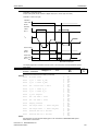
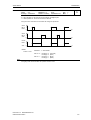
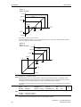
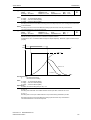
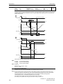
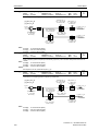
r0052 Bit03 "Drive fault active"
Output of Bit3 (Fault) will be inverted on digital output (Low = Fault, High = No Fault).
r0052 Bit14 "Motor runs right"
ON/OFF1
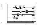
r0054 ON
Bit 00
t
Reverse
r0054
Bit 11
t
f act
0
t
Drive running
r0052
Bit 02
t
Motor runs
r0052 right
Bit 14 left
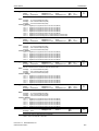
t
not defined
last state is displayed
The display segments for the status word are shown in the "Introduction to MICROMASTER System
Parameters".
r0053
CO/BO: Act. status word 2
Datatype: U16
Min:
Def:
Max:
Unit: -
P-Group: COMMANDS
Displays second status word of inverter (in bit format).
Bitfields:
Bit00
DC brake active
Bit01
f_act
>
P2167 (f_off)
Bit02
f_act
>= P1080 (f_min)
Bit03
Act. current r0027 >= P2170
Bit04
f_act
>
Bit05
f_act
<= P2155 (f_1)
Bit06
f_act>= setpoint
Bit07
Act. Vdc r0026 <
P2172
Bit08
Act. Vdc r0026 >
P2172
Bit09
Ramping finished
Bit10
PID output r2294
==
P2292 (PID_min)
Bit11
PID output r2294
==
P2291 (PID_max)
Bit14
Download data set 0 from AOP
Bit15
Download data set 1 from AOP
P2155 (f_1)
0
1
0
1
0
1
0
1
0
1
0
1
0
1
0
1
0
1
0
1
0
1
0
1
0
1
0
1
-
Level:
3
NO
YES
NO
YES
NO
YES
NO
YES
NO
YES
NO
YES
NO
YES
NO
YES
NO
YES
NO
YES
NO
YES
NO
YES
NO
YES
NO
YES
Details:
See description of seven-segment display given in the "Introduction to MICROMASTER System
Parameters" in this manual.
Parameter List MICROMASTER 430
6SE6400-5AF00-0BP0
25
Parameters
r0054
Issue 08/02
CO/BO: Act. control word 1
Datatype: U16
Unit: -
P-Group: COMMANDS
Min:
Def:
Max:
-
Level:
3
Displays first control word of inverter and can be used to diagnose which commands are active.
Bitfields:
Bit00
ON/OFF1
0
NO
1
YES
Bit01
OFF2: Electrical stop
0
YES
1
NO
Bit02
OFF3: Fast stop
0
YES
1
NO
Bit03
Pulse enable
0
NO
1
YES
Bit04
RFG enable
0
NO
1
YES
Bit05
RFG start
0
NO
1
YES
Bit06
Setpoint enable
0
NO
1
YES
Bit07
Fault acknowledge
0
NO
1
YES
Bit08
JOG right
0
NO
1
YES
Bit09
JOG left
0
NO
1
YES
Bit10
Control from PLC
0
NO
1
YES
Bit11
Reverse (setpoint inversion)
0
NO
1
YES
Bit13
Motor potentiometer MOP up
0
NO
1
YES
Bit14
Motor potentiometer MOP down
0
NO
1
YES
Bit15
CDS Bit 0 (Local/Remote)
0
NO
1
YES
Details:
See description of seven-segment display given in the "Introduction to MICROMASTER System
Parameters" in this manual.
r0055
CO/BO: Act. control word 2
Datatype: U16
P-Group: COMMANDS
Unit: -
Min:
Def:
Max:
-
Level:
3
Displays additional control word of inverter and can be used to diagnose which commands are active.
Bitfields:
Bit00
Fixed frequency Bit 0
0
NO
1
YES
Bit01
Fixed frequency Bit 1
0
NO
1
YES
Bit02
Fixed frequency Bit 2
0
NO
1
YES
Bit03
Fixed frequency Bit 3
0
NO
1
YES
Bit04
Drive data set (DDS) Bit 0
0
NO
1
YES
Bit05
Drive data set (DDS) Bit 1
0
NO
1
YES
Bit08
PID enabled
0
NO
1
YES
Bit09
DC brake enabled
0
NO
1
YES
Bit11
Droop
0
NO
1
YES
Bit12
Torque control
0
NO
1
YES
Bit13
External fault 1
0
YES
1
NO
Bit15
Command data set (CDS) Bit 1
0
NO
1
YES
Details:
See description of seven-segment display given in the "Introduction to MICROMASTER System
Parameters" in this handbook.
Parameter List
26
MICROMASTER 430
6SE6400-5AF00-0BP0
Issue 08/02
r0056
Parameters
CO/BO: Status of motor control
Datatype: U16
Unit: -
P-Group: CONTROL
Min:
Def:
Max:
-
Level:
3
Displays status of motor control (MM420: V/f status), which can be used to diagnose inverter status.
Bitfields:
Bit00
Init. control finished
0
NO
1
YES
Bit01
Motor demagnetizing finished
0
NO
1
YES
Bit02
Pulses enabled
0
NO
1
YES
Bit03
Voltage soft start select
0
NO
1
YES
Bit04
Motor excitation finished
0
NO
1
YES
Bit05
Starting boost active
0
NO
1
YES
Bit06
Acceleration boost active
0
NO
1
YES
Bit07
Frequency is negative
0
NO
1
YES
Bit08
Field weakening active
0
NO
1
YES
Bit09
Volts setpoint limited
0
NO
1
YES
Bit10
Slip frequency limited
0
NO
1
YES
Bit11
F_out > F_max Freq. limited
0
NO
1
YES
Bit12
Phase reversal selected
0
NO
1
YES
Bit13
I-max controller active
0
NO
1
YES
Bit14
Vdc-max controller active
0
NO
1
YES
Bit15
KIB (Vdc-min control) active
0
NO
1
YES
Details:
See description of seven-segment display given in the introduction.
r0061
Min:
Def:
Max:
-
Level:
Unit: Hz
Unit: Hz
Min:
Def:
Max:
-
Level:
Datatype: Float
Unit: %
Min:
Def:
Max:
-
Level:
Datatype: Float
-
Level:
CO: Act. rotor speed
Datatype: Float
P-Group: CONTROL
3
Displays current speed detected by encoder.
r0063
CO: Act. frequency
P-Group: CONTROL
3
Displays actual speed.
r0065
CO: Slip frequency
P-Group: CONTROL
3
Displays slip frequency of motor in [%] relative to the rated motor frequency (P0310).
Details:
For V/f control, see also P1335 (slip compensation).
r0067
CO: Act. output current limit
Datatype: Float
P-Group: CONTROL
Unit: A
Min:
Def:
Max:
3
Displays valid maximum output current of inverter.
This value is influenced by P0640 (max. output current), the derating characteristics and the thermal motor
and inverter protection.
Dependency:
P0610 (motor I2t temperature reaction) defines reaction when limit is reached.
Note:
Normally, current limit = rated motor current (P0305) x motor current limit (P0640). It is less than or equal to
maximum inverter current r0209.
The current limit may be reduced if the motor thermal model calculation indicates that overheating will
occur.
Parameter List MICROMASTER 430
6SE6400-5AF00-0BP0
27
Parameters
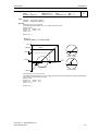
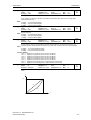
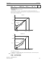
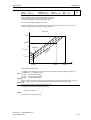
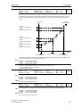
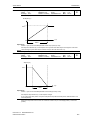
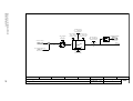
r0071
Issue 08/02
CO: Max. output voltage
Datatype: Float
Min:
Def:
Max:
Unit: V
P-Group: CONTROL
-
Level:
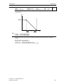
3
Displays maximum output voltage.
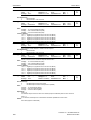
V
r0071
Vmax
(Inverter)
Vmax = f(Vdc,MODmax)
Vout
(Inverter)
P0304
Vn
(Motor)
f
P0310
fn
(Motor)
P, ψ
Power
Flux
~
1
f
f
Field weakening
Dependency:
Actual maximum output voltage depends on the actual input supply voltage.
r0080
Unit: Nm
Min:
Def:
Max:
-
Level:
Datatype: Float
Unit: A
Min:
Def:
Max:
-
Level:
Datatype: Float
CO: Act. torque
P-Group: CONTROL
3
Displays actual torque.
r0086
CO: Act. active current
P-Group: CONTROL
3
Displays active (real part) of motor current.
Dependency:
Applies when V/f control is selected in P1300 (control mode); otherwise, the display shows the value zero.
Level:
P0095[10] CI: Display PZD signals
Min: 0:0
CStat:
CT
Datatype: U32
Unit: Def:
0:0
P-Group: CONTROL
Active: first confirm
QuickComm. No
Max: 4000:0
3
Selects source of display for PZD signals.
Index:
P0095[0]
P0095[1]
P0095[2]
P0095[3]
P0095[4]
P0095[5]
P0095[6]
P0095[7]
P0095[8]
P0095[9]
:
:
:
:
:
:
:
:
:
:
1st PZD signal
2nd PZD signal
3rd PZD signal
4th PZD signal
5th PZD signal
6th PZD signal
7th PZD signal
8th PZD signal
9th PZD signal
10th PZD signal
Parameter List
28
MICROMASTER 430
6SE6400-5AF00-0BP0
Issue 08/02
r0096[10]
Parameters
PZD signals
Datatype: Float
Unit: %
P-Group: CONTROL
Min:
Def:
Max:
-
Level:
Min:
Def:
Max:
0
0
2
Level:
3
Displays PZD signals in [%].
Index:
r0096[0]
r0096[1]
r0096[2]
r0096[3]
r0096[4]
r0096[5]
r0096[6]
r0096[7]
r0096[8]
r0096[9]
:
:
:
:
:
:
:
:
:
:
1st PZD signal
2nd PZD signal
3rd PZD signal
4th PZD signal
5th PZD signal
6th PZD signal
7th PZD signal
8th PZD signal
9th PZD signal
10th PZD signal
Note:
r0096 = 100 % corresponds to 4000 hex.
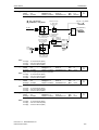
P0100
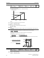
Europe / North America
CStat:
C
P-Group: QUICK
Datatype: U16
Active: first confirm
Unit: QuickComm. Yes
1
Determines whether power settings (e.g. nominal rating plate power - P0307) are expressed in [kW] or [hp].
Remove I/O board
The default settings for the nominal rating plate frequency (P0310) and maximum motor frequency (P1082)
are also set automatically here, in addition to reference frequency (P2000).
Possible Settings:
0
Europe [kW],
frequency default 50 Hz
1
North America [hp], frequency default 60 Hz
2
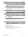
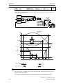
North America [kW], frequency default 60 Hz
Dependency:
The setting of DIP switch 2 under the I/O board determines the validity of settings 0 and 1 for P0100
according to the diagram below:
Parameter List MICROMASTER 430
6SE6400-5AF00-0BP0
DIP2
29
Parameters
Issue 08/02
Quick
commissioning
P0010 = 1
Power
cycle
P0100 = 2
?
yes
yes
no
no
no
DIP2 = OFF
?
P0100 = 2
?
P0100 = 1
?
yes
no
yes
Power in kW
Frequency 50 Hz
Power in kW
Frequency 60 Hz
Power in hp
Frequency 60 Hz
P0100 = 0
P0100 = 2
P0100 = 1
Stop drive first (i.e. disable all pulses) before you change this parameter.
P0010 = 1 (commissioning mode) enables changes to be made.
Changing P0100 resets all rated motor parameters as well as other parameters that depend on the rated
motor parameters (see P0340 - calculation of motor parameters).
Notice:
P0199
P0100 setting 2 (==> [kW], frequency default 60 [Hz]) is not overwritten by the setting of DIP switch 2 (see
diagram above).
Level:
Equipment system number
Min: 0
CStat:
UT
Datatype: U16
Unit: Def:
0
P-Group: Active: first confirm
QuickComm. No
Max: 255
2
Equipment system number. This parameter has no operation effect.
Parameter List
30
MICROMASTER 430
6SE6400-5AF00-0BP0
Issue 08/02
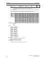
r0200
Parameters
Act. power stack code number
Datatype: U32
Min:
Def:
Max:
Unit: -
P-Group: INVERTER
Level:
-
3
Identifies hardware variant as shown in table below.
CodeNo.
MM430
MLFB
Internal Protection Frame
Size
Degree
Filter
Input Voltage & Frequency
VT Power
kW
271 6SE6430-2UD27-5CA0
3AC380-480V +10% -10% 47-63Hz
7,5
no
IP20
C
272 6SE6430-2UD31-1CA0
3AC380-480V +10% -10% 47-63Hz
11
no
IP20
C
273 6SE6430-2UD31-5CA0
C
3AC380-480V +10% -10% 47-63Hz
15
no
IP20
274 6SE6430-2AD27-5CA0 3AC380-480V +10% -10% 47-63Hz
7,5
Cl. A
IP20
C
275 6SE6430-2AD31-1CA0 3AC380-480V +10% -10% 47-63Hz
11
Cl. A
IP20
C
C
276 6SE6430-2AD31-5CA0 3AC380-480V +10% -10% 47-63Hz
15
Cl. A
IP20
277 6SE6430-2UD31-8DA0
3AC380-480V +10% -10% 47-63Hz
18,5
no
IP20
D
278 6SE6430-2UD32-2DA0
3AC380-480V +10% -10% 47-63Hz
22
no
IP20
D
279 6SE6430-2UD33-0DA0
3AC380-480V +10% -10% 47-63Hz
D
30
no
IP20
280 6SE6430-2AD31-8DA0 3AC380-480V +10% -10% 47-63Hz
18,5
Cl. A
IP20
D
281 6SE6430-2AD32-2DA0 3AC380-480V +10% -10% 47-63Hz
22
Cl. A
IP20
D
282 6SE6430-2AD33-0DA0 3AC380-480V +10% -10% 47-63Hz
30
Cl. A
IP20
D
283 6SE6430-2UD33-7EA0
3AC380-480V +10% -10% 47-63Hz
37
no
IP20
E
284 6SE6430-2UD34-5EA0
3AC380-480V +10% -10% 47-63Hz
45
no
IP20
E
285 6SE6430-2AD33-7EA0
3AC380-480V +10% -10% 47-63Hz
37
Cl. A
IP20
E
286 6SE6430-2AD34-5EA0
3AC380-480V +10% -10% 47-63Hz
45
Cl. A
IP20
E
287 6SE6430-2UD35-5FA0
3AC380-480V +10% -10% 47-63Hz
55
no
IP20
F
288 6SE6430-2UD37-5FA0
3AC380-480V +10% -10% 47-63Hz
75
no
IP20
F
289 6SE6430-2UD38-8FA0
3AC380-480V +10% -10% 47-63Hz
90
no
IP20
F
290 6SE6430-2AD35-5FA0
3AC380-480V +10% -10% 47-63Hz
55
Cl. A
IP20
F
291 6SE6430-2AD37-5FA0
3AC380-480V +10% -10% 47-63Hz
75
Cl. A
IP20
F
292 6SE6430-2AD38-8FA0
3AC380-480V +10% -10% 47-63Hz
90
Cl. A
IP20
F
Notice:
Parameter r0200 = 0 indicates that no power stack has been identified.
P0201
Min:
Def:
Max:
0
0
65535
Level:
Min:
Def:
Max:
-
Level:
Unit: -
Min:
Def:
Max:
-
Level:
Unit: -
Power stack code number
CStat:
C
P-Group: INVERTER
Datatype: U16
Active: first confirm
Unit: QuickComm. No
3
Confirms actual power stack identified.
r0203
Act. inverter type
Datatype: U16
P-Group: INVERTER
3
Type number of actual inverter identified.
Possible Settings:
1
MICROMASTER 420
2
MICROMASTER 440
3
MICRO- / COMBIMASTER 411
4
MICROMASTER 410
5
Reserved
6
MICROMASTER 440 PX
7
MICROMASTER 430
8
MICROMASTER 430 PX
r0204
Power stack features
Datatype: U32
P-Group: INVERTER
Displays hardware features of power stack.
Bitfields:
Bit00
DC input voltage
Bit01
RFI filter
0
1
0
1
3
NO
YES
NO
YES
Note:
Parameter r0204 = 0 indicates that no power stack has been identified.
Parameter List MICROMASTER 430
6SE6400-5AF00-0BP0
31
Parameters
r0206
Issue 08/02
Rated inverter power [kW] / [hp]
Datatype: Float
Min:
Def:
Max:
Unit: -
P-Group: INVERTER
-
Level:
3
Displays nominal rated motor power from inverter.
Dependency:
Value is displayed in [kW] or [hp] depending on setting for P0100 (operation for Europe / North America).
Level:
r0207
Rated inverter current
Min: Datatype: Float
Unit: A
Def:
P-Group: INVERTER
Max: -
3
Displays maximum continuous output current of inverter.
r0208
Min:
Def:
Max:
-
Level:
Unit: V
Min:
Def:
Max:
-
Level:
Unit: A
Rated inverter voltage
Datatype: U32
P-Group: INVERTER
3
Displays nominal AC supply voltage of inverter.
Value:
r0208 = 230 : 200 - 240 V +/- 10 %
r0208 = 400 : 380 - 480 V +/- 10 %
r0208 = 575 : 500 - 600 V +/- 10 %
r0209
Maximum inverter current
Datatype: Float
P-Group: INVERTER
3
Displays maximum output current of inverter.
Dependency:
Parameter r0209 depends on the derating which is affected by pulse frequency P1800, ambient
temperature and altitude. The data of deration is given in the OPERATING INSRTRUCTION.
P0210
Supply voltage
CStat:
CT
P-Group: INVERTER
Datatype: U16
Active: Immediately
Unit: V
QuickComm. No
Min:
Def:
Max:
0
230
1000
Level:
3
Optimizes Vdc controller, which extends the ramp-down time if regenerative energy from motor would
otherwise cause DC link overvoltage trips.
Reducing the value enables controller to cut in earlier and reduce the risk of overvoltage.
Dependency:
Set P1254 ("Auto detect Vdc switch-on levels") = 0. Cut-in levels for Vdc-controller and compound braking
are then derived directly from P0210 (supply voltage).
Vdc_max switch-on level
= 1.15 ⋅ 2 ⋅ P0210
Compound braking switch-on level
= 1.13 ⋅ 2 ⋅ P0210
Note:
r0231[2]
If mains voltage is higher than value entered, automatic deactivation of the Vdc controller may occur to
avoid acceleration of the motor. An alarm will be issued in this case (A0910).
Level:
Max. cable length
Min: Datatype: U16
Unit: m
Def:
P-Group: INVERTER
Max: -
3
Indexed parameter to display maximum allowable cable length between inverter and motor.
Index:
r0231[0] : Max. allowed unscreened cable length
r0231[1] : Max. allowed screened cable length
Notice:
For full EMC compliance, the screened cable must not exceed 25 m in length when an EMC filter is fitted.
Parameter List
32
MICROMASTER 430
6SE6400-5AF00-0BP0
Issue 08/02
P0290
Parameters
Inverter overload reaction
CStat:
CT
P-Group: INVERTER
Datatype: U16
Active: first confirm
Unit: QuickComm. No
Min:
Def:
Max:
0
2
3
Level:
3
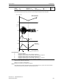
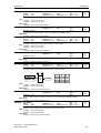
Selects reaction of inverter to an internal over-temperature.
Following physical values influence the inverter overload protection (see diagram):
- heat sink temperature
- junction temperature (IGBT temperature)
- inverter I²t
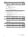
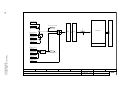
Inverter overload reaction
P0290
i2t
Heat sink
temperature
A0504
i_max
control
A0505
A0506
Inverter
thermal
model
IGBT
temperature
f_pulse
control
F0004
F0005
Possible Settings:
0
Reduce output frequency
1
Trip (F0004)
2
Reduce pulse frequency and output frequency
3
Reduce pulse frequency then trip (F0004)
Notice:
P0290 = 0:
Reduction of output frequency is usually only effective if the load is also reduced. This is for example valid
for variable torque applications with a quadratic torque characteristic as pumps or fans.
A trip will always result eventually, if the action taken does not sufficiently reduce internal temperature.
P0291[3]
The pulse frequency P1800 is normally reduced only if higher than 2 kHz. The actual pulse frequency is
displayed in parameter r1801.
Level:
Inverter protection
Min: 0
CStat:
CT
Datatype: U16
Unit: Def:
1
P-Group: INVERTER
Active: Immediately
QuickComm. No
Max: 7
3
Control bit 0 for enabling/disabling automatic pulse frequency reduction at output frequencies below 2 Hz.
Bit 2 shows if phase loss dedection (input phase) of 3 phase inverters is enabled after factory reset. Default
setting of phase loss is disabled for FSA - FSC. FSD and greater it is enabled.
Bitfields:
Bit00
Pulse frequency reduced below 2Hz
0
NO
1
YES
Bit01
Reserved
0
NO
1
YES
Bit02
Phase loss detection enable
0
NO
1
YES
Index:
P0291[0] : 1st. Drive data set (DDS)
P0291[1] : 2nd. Drive data set (DDS)
P0291[2] : 3rd. Drive data set (DDS)
Details:
See P0290 (inverter overload reaction)
Level:
P0292
Inverter overload warning
Min: 0
CStat:
CUT
Datatype: U16
Unit: °C
Def:
15
P-Group: INVERTER
Active: first confirm
QuickComm. No
Max: 25
3
P0295
Defines temperature difference (in [°C]) between inverter over-temperature trip and warning thresholds.
Level:
Min: 0
CStat:
CUT
Datatype: U16
Unit: s
Def:
0
P-Group: TERMINAL
Active: first confirm
QuickComm. No
Max: 3600
Inverter fan off delay time
3
Defines inverter fan switch off delay time in seconds after drive has stopped.
Note:
Setting to 0, inverter fan will switch off when the drive stops, that is no delay.
Parameter List MICROMASTER 430
6SE6400-5AF00-0BP0
33
Parameters
P0304[3]
Issue 08/02
Rated motor voltage
CStat:
C
P-Group: MOTOR
Datatype: U16
Active: first confirm
Min:
Def:
Max:
Unit: V
QuickComm. Yes
Level:
10
230
2000
1
Nominal motor voltage [V] from rating plate. Following diagram shows a typical rating plate with the
locations of the relevant motor data.
P0305
P0310
P0304
3~Mot
1LA7130-4AA10
No UD 0013509-0090-0031
P0307
TICI F
1325
EN 60034
IP 55
IM B3
50 Hz
230-400 V
60 Hz
460 V
5.5kW
19.7/11.A
6.5kW
10.9 A
Cos ϕ=0.81
1455/min
Cos ϕ=0.82
1755/min
==∆/Υ
==∆/Υ=
∆/Υ=220-240/380-420 V
Υ=440-480
19.7-20.6/11.4-11.9 A
11.1-11.3 A
P0308
95.75%
45kg
P0311
P0309
Index:
P0304[0] : 1st. Drive data set (DDS)
P0304[1] : 2nd. Drive data set (DDS)
P0304[2] : 3rd. Drive data set (DDS)
Dependency:
Changeable only when P0010 = 1 (quick commissioning).
Caution:
The input of rating plate data must correspond with the wiring of the motor (star / delta). This means, if delta
wiring is used for the motor, delta rating plate data has to be entered.
Three-phase motor connection
3AC 230/400 V
W2
U1
U2
V1
3AC 400 V
W2
U2
U1
V1
V2
V2
Line
U1
Delta connection
V2
U1
V1
W1
Line
400 V
U1
V1
W1
U2
W1
W1
230 V
W2
U1
V1
W1
V1
W1
Star connection
Delta connection
Parameter List
34
MICROMASTER 430
6SE6400-5AF00-0BP0
Issue 08/02
P0305[3]
Parameters
Rated motor current
CStat:
C
P-Group: MOTOR
Datatype: Float
Active: first confirm
Unit: A
QuickComm. Yes
Min:
Def:
Max:
0.01
3.25
10000.00
Level:
1
Nominal motor current [A] from rating plate - see diagram in P0304.
Index:
P0305[0] : 1st. Drive data set (DDS)
P0305[1] : 2nd. Drive data set (DDS)
P0305[2] : 3rd. Drive data set (DDS)
Dependency:
Changeable only when P0010 = 1 (quick commissioning).
Depends also on P0320 (motor magnetization current).
Note:
The maximum value of P0305 depends on the maximum inverter current r0209 and the motor type:
Asynchronous motor : P0305 max, asyn = r0209
Synchronous motor : P0305 max, syn = 2 ⋅ r0209
It is recommanded that the ratio of P0305 (rated motor current) and r0207 (rated inverter current) should not
be lower than:
U/f and FCC :
P0307[3]
1 P0305
≤
8
r0207
Rated motor power
CStat:
C
P-Group: MOTOR
Datatype: Float
Active: first confirm
Unit: QuickComm. Yes
Min:
Def:
Max:
0.01
0.75
2000.00
Level:
Min:
Def:
Max:
0.000
0.000
1.000
Level:
Min:
Def:
Max:
0.0
0.0
99.9
Level:
1
Nominal motor power [kW/hp] from rating plate.
Index:
P0307[0] : 1st. Drive data set (DDS)
P0307[1] : 2nd. Drive data set (DDS)
P0307[2] : 3rd. Drive data set (DDS)
Dependency:
If P0100 = 1, values will be in [hp] - see diagram P0304 (rating plate).
Changeable only when P0010 = 1 (quick commissioning).
P0308[3]
Rated motor cosPhi
CStat:
C
P-Group: MOTOR
Datatype: Float
Active: first confirm
Unit: QuickComm. Yes
3
Nominal motor power factor (cosPhi) from rating plate - see diagram P0304.
Index:
P0308[0] : 1st. Drive data set (DDS)
P0308[1] : 2nd. Drive data set (DDS)
P0308[2] : 3rd. Drive data set (DDS)
Dependency:
Changeable only when P0010 = 1 (quick commissioning).
Visible only when P0100 = 0 or 2, (motor power entered in [kW]).
Setting 0 causes internal calculation of value (see r0332).
P0309[3]
Rated motor efficiency
CStat:
C
P-Group: MOTOR
Datatype: Float
Active: first confirm
Unit: %
QuickComm. Yes
3
Nominal motor efficiency in [%] from rating plate.
Index:
P0309[0] : 1st. Drive data set (DDS)
P0309[1] : 2nd. Drive data set (DDS)
P0309[2] : 3rd. Drive data set (DDS)
Dependency:
Changeable only when P0010 = 1 (quick commissioning).
Visible only when P0100 = 1, (i.e. motor power entered in [hp]).
Setting 0 causes internal calculation of value (see r0332).
Note:
P0309 = 100 % corresponds to superconducting.
Details:
See diagram in P0304 (rating plate).
Parameter List MICROMASTER 430
6SE6400-5AF00-0BP0
35
Parameters
P0310[3]
Issue 08/02
Rated motor frequency
CStat:
C
P-Group: MOTOR
Datatype: Float
Active: first confirm
Unit: Hz
QuickComm. Yes
Min:
Def:
Max:
12.00
50.00
650.00
Level:
Min:
Def:
Max:
0
0
40000
Level:
-
Level:
1
Nominal motor frequency [Hz] from rating plate.
Index:
P0310[0] : 1st. Drive data set (DDS)
P0310[1] : 2nd. Drive data set (DDS)
P0310[2] : 3rd. Drive data set (DDS)
Dependency:
Changeable only when P0010 = 1 (quick commissioning).
Pole pair number recalculated automatically if parameter is changed.
Details:
See diagram in P0304 (rating plate)
P0311[3]
Rated motor speed
CStat:
C
P-Group: MOTOR
Datatype: U16
Active: first confirm
Unit: 1/min
QuickComm. Yes
1
Nominal motor speed [rpm] from rating plate.
Index:
P0311[0] : 1st. Drive data set (DDS)
P0311[1] : 2nd. Drive data set (DDS)
P0311[2] : 3rd. Drive data set (DDS)
Dependency:
Changeable only when P0010 = 1 (quick commissioning).
Setting 0 causes internal calculation of value.
Required for vector control and V/f control with speed controller.
Slip compensation in V/f control requires rated motor speed for correct operation.
Pole pair number recalculated automatically if parameter is changed.
Details:
See diagram in P0304 (rating plate)
r0313[3]
Motor pole pairs
Datatype: U16
P-Group: MOTOR
Unit: -
Min:
Def:
Max:
3
Displays number of motor pole pairs that the inverter is currently using for internal calculations.
Index:
r0313[0] : 1st. Drive data set (DDS)
r0313[1] : 2nd. Drive data set (DDS)
r0313[2] : 3rd. Drive data set (DDS)
Value:
r0313 = 1 : 2-pole motor
r0313 = 2 : 4-pole motor
etc.
Dependency:
Recalculated automatically when P0310 (rated motor frequency) or P0311 (rated motor speed) is changed.
Level:
P0320[3]
Motor magnetizing current
Min: 0.0
CStat:
CT
Datatype: Float
Unit: %
Def:
0.0
P-Group: MOTOR
Active: Immediately
QuickComm. Yes
Max: 99.0
3
Defines motor magnetization current in [%] relative to P0305 (rated motor current).
Index:
P0320[0] : 1st. Drive data set (DDS)
P0320[1] : 2nd. Drive data set (DDS)
P0320[2] : 3rd. Drive data set (DDS)
Dependency:
P0320 = 0:
Setting 0 causes calculation by P0340 = 1 (data entered from rating plate) or by P3900 = 1 - 3 (end of quick
commissioning). The calculated value is displayed in parameter r0331.
Parameter List
36
MICROMASTER 430
6SE6400-5AF00-0BP0
Issue 08/02
r0330[3]
Parameters
Rated motor slip
Datatype: Float
Unit: %
P-Group: MOTOR
Min:
Def:
Max:
-
Level:
3
Displays nominal motor slip in [%] relative to P0310 (rated motor frequency) and P0311 (rated motor
speed).
r0330 [%] =
P0311
⋅ r0313
60
⋅ 100 %
P0310
P0310 −
Index:
r0330[0] : 1st. Drive data set (DDS)
r0330[1] : 2nd. Drive data set (DDS)
r0330[2] : 3rd. Drive data set (DDS)
r0331[3]
Min:
Def:
Max:
-
Level:
Unit: A
Min:
Def:
Max:
-
Level:
Unit: -
Rated magnetization current
Datatype: Float
P-Group: MOTOR
3
Displays calculated magnetizing current of motor in [A].
Index:
r0331[0] : 1st. Drive data set (DDS)
r0331[1] : 2nd. Drive data set (DDS)
r0331[2] : 3rd. Drive data set (DDS)
r0332[3]
Rated power factor
Datatype: Float
P-Group: MOTOR
3
Displays power factor for motor
Index:
r0332[0] : 1st. Drive data set (DDS)
r0332[1] : 2nd. Drive data set (DDS)
r0332[2] : 3rd. Drive data set (DDS)
Dependency:
Value is calculated internally if P0308 (rated motor cosPhi) set to 0; otherwise, value entered in P0308 is
displayed.
Level:
P0335[3]
Motor cooling
Min: 0
CStat:
CT
Datatype: U16
Unit: Def:
0
P-Group: MOTOR
Active: first confirm
QuickComm. Yes
Max: 3
3
Selects motor cooling system used.
Possible Settings:
0
Self-cooled: Using shaft mounted fan attached to motor
1
Force-cooled: Using separately powered cooling fan
2
Self-cooled and internal fan
3
Force-cooled and internal fan
Index:
P0335[0] : 1st. Drive data set (DDS)
P0335[1] : 2nd. Drive data set (DDS)
P0335[2] : 3rd. Drive data set (DDS)
Caution:
The following combination of parameter setting should not be combined:
P0610 = 1 and P0335 = 0 or 2 :
When P0335 = 0 or 2 the inverter cools the motor using a shaft mounted fan. If this is used in conjunction
with P0610 the cooling of the motor will be inefficient.
In essence, if the i2t calculation reduces the output frequency, then the shaft mounted fan will also reduce
its cooling effect, the motor will then eventually overheat and trip.
Exception:
Applications with variable torque the reduction of max. current leeds automatically to a reduction of the load
/ output current.
Notice:
Motors of series 1LA1 and 1LA8 have an internal fan. This internal motor fan must not be confused with the
fan at the end of the motor shaft.
Parameter List MICROMASTER 430
6SE6400-5AF00-0BP0
37
Parameters
P0340[3]
Issue 08/02
Calculation of motor parameters
CStat:
CT
P-Group: MOTOR
Datatype: U16
Active: first confirm
Unit: QuickComm. No
Min:
Def:
Max:
0
0
4
Level:
1.0
9.4
6500.0
Level:
3
Calculates various motor parameters, including:
P0344 Motor weight
P0346 Magnetization time
P0347 Demagnetization time
P0350 Stator resistance
P0611 Motor I2t time constant
P1253 Vdc-controller output limitation
P1316 Boost end frequency
P2000 Reference frequency
P2002 Reference current
Possible Settings:
0
No calculation
1
Complete parameterization
2
Calculation of equivalent circuit data
3
Calculation of V/f data
4
Calculation of controller settings only
Index:
P0340[0] : 1st. Drive data set (DDS)
P0340[1] : 2nd. Drive data set (DDS)
P0340[2] : 3rd. Drive data set (DDS)
Note:
This parameter is required during commissioning to optimize inverter performance.
P0344[3]
Motor weight
CStat:
CUT
P-Group: MOTOR
Datatype: Float
Active: Immediately
Unit: kg
QuickComm. No
Min:
Def:
Max:
3
Specifies motor weight [kg].
Index:
P0344[0] : 1st. Drive data set (DDS)
P0344[1] : 2nd. Drive data set (DDS)
P0344[2] : 3rd. Drive data set (DDS)
Note:
This value is used in the motor thermal model.
P0346[3]
It is normally calculated automatically from P0340 (motor parameters) but can also be entered manually.
Level:
Min: 0.000
CStat:
CUT
Datatype: Float
Unit: s
Def:
1.000
P-Group: MOTOR
Active: Immediately
QuickComm. No
Max: 20.000
Magnetization time
3
Sets magnetization time [s], i.e. waiting time between pulse enable and start of ramp-up. Motor
magnetization builds up during this time.
Magnetization time is normally calculated automatically from the motor data and corresponds to the rotor
time constant (r0384).
Index:
P0346[0] : 1st. Drive data set (DDS)
P0346[1] : 2nd. Drive data set (DDS)
P0346[2] : 3rd. Drive data set (DDS)
Note:
If boost settings are higher than 100 %, magnetization may be reduced.
Notice:
An excessive reduction of this time can result in insufficient motor magnetization.
P0347[3]
Demagnetization time
CStat:
CUT
P-Group: MOTOR
Datatype: Float
Active: Immediately
Unit: s
QuickComm. No
Min:
Def:
Max:
0.000
1.000
20.000
Level:
3
Changes time allowed after OFF2 / fault condition, before pulses can be re-enabled.
Index:
P0347[0] : 1st. Drive data set (DDS)
P0347[1] : 2nd. Drive data set (DDS)
P0347[2] : 3rd. Drive data set (DDS)
Note:
The demagnetization time is approximately 2.5 x rotor time constant (r0384) in seconds.
Notice:
Not active following a normally completed ramp-down, e.g. after OFF1, OFF3 or JOG.
Overcurrent trips will occur if the time is decreased excessively.
Parameter List
38
MICROMASTER 430
6SE6400-5AF00-0BP0
Issue 08/02
P0350[3]
Parameters
Stator resistance (line-to-line)
CStat:
CUT
P-Group: MOTOR
Datatype: Float
Active: Immediately
Unit: Ohm
QuickComm. No
Min:
Def:
Max:
0.00001
4.00000
2000.00000
Level:
3
Stator resistance value in [Ohms] for connected motor (from line-to-line). The parameter value includes the
cable resistance.
There are three ways to determine the value for this parameter:
1. Calculate using
P0340 = 1 (data entered from rating plate) or
P0010 = 1, P3900 = 1,2 or 3 (end of quick commissioning).
2. Measure using P1910 = 1 (motor data identification - value for stator resistance is overwritten).
3. Measure manually using an Ohmmeter.
Index:
P0350[0] : 1st. Drive data set (DDS)
P0350[1] : 2nd. Drive data set (DDS)
P0350[2] : 3rd. Drive data set (DDS)
Note:
Since measured line-to-line, this value may appear to be higher (up to 2 times higher) than expected.
The value entered in P0350 (stator resistance) is the one obtained by the method last used.
P0352[3]
Cable resistance
CStat:
CUT
P-Group: MOTOR
Datatype: Float
Active: Immediately
Unit: Ohm
QuickComm. No
Min:
Def:
Max:
0.0
0.0
120.0
Level:
3
Describes cable resistance between inverter and motor for one phase.
The value corresponds to the resistance of the cable between the inverter and the motor, relative to the
rated impedance.
Index:
P0352[0] : 1st. Drive data set (DDS)
P0352[1] : 2nd. Drive data set (DDS)
P0352[2] : 3rd. Drive data set (DDS)
r0384[3]
Min:
Def:
Max:
-
Level:
Unit: ms
Min:
Def:
Max:
-
Level:
Unit: %
-
Level:
Rotor time constant
Datatype: Float
P-Group: MOTOR
3
Displays calculated rotor time constant [ms].
Index:
r0384[0] : 1st. Drive data set (DDS)
r0384[1] : 2nd. Drive data set (DDS)
r0384[2] : 3rd. Drive data set (DDS)
r0395
CO: Total stator resistance [%]
Datatype: Float
P-Group: MOTOR
3
Displays stator resistance of motor as [%] of combined stator/cable resistance.
Note:
100 % means : Z
ratedmot ⋅
r0396
P 0304
P 0305
CO: Act. rotor resistance
Datatype: Float
P-Group: MOTOR
Unit: %
Min:
Def:
Max:
3
Displays (adapted) rotor resistance of the motor equivalent circuit (phase value) in [%].
Note:
100 % means : Z
ratedmot ⋅
P 0304
P 0305
Notice:
Values greater than 25 % tend to produce excessive motor slip. Check rated motor speed [rpm] value
(P0311).
Parameter List MICROMASTER 430
6SE6400-5AF00-0BP0
39
Parameters
P0400[3]
Issue 08/02
Select encoder type
CStat:
CT
P-Group: ENCODER
Datatype: U16
Active: Immediately
Min:
Def:
Max:
Unit: QuickComm. No
0
0
2
Level:
3
Selects encoder type.
Parameter
Terminal
P0400 = 1
A
Single ended
A
Differential
Track
Encoder type
AN
P0400 = 2
Single ended
A
B
A
Differential
AN
B
BN
Possible Settings:
0
Disabled
1
Single channel encoder
2
Quadrature encoder without zero pulse
Index:
P0400[0] : 1st. Drive data set (DDS)
P0400[1] : 2nd. Drive data set (DDS)
P0400[2] : 3rd. Drive data set (DDS)
Note:
Encoders with zero pulse can also be connected, but the zero pulse is not used in MM4.
The term "quadrature" in setting 2 refers to two periodic functions separated by a quarter cycle or 90
degrees.
r0403
CO/BO: Encoder status word
Datatype: U16
Min:
Def:
Max:
Unit: -
P-Group: COMMANDS
Displays status word of encoder (in bit format).
Bitfields:
Bit00
Encoder module active
Bit01
Encoder error
Bit02
Signal o.k.
Bit03
Encoder low speed loss
Bit04
HW timer used
0
1
0
1
0
1
0
1
0
1
-
Level:
3
NO
YES
NO
YES
NO
YES
NO
YES
NO
YES
Details:
See description of seven-segment display given in the "Introduction to MICROMASTER System
Parameters" in this manual.
Parameter List
40
MICROMASTER 430
6SE6400-5AF00-0BP0
Issue 08/02
P0408[3]
Parameters
Encoder pulses per revolution
CStat:
CT
P-Group: ENCODER
Datatype: U16
Active: Immediately
Unit: QuickComm. No
Min:
Def:
Max:
2
1024
20000
Level:
3
Specifies the number of encoder pulses per revolution.
Index:
P0408[0] : 1st. Drive data set (DDS)
P0408[1] : 2nd. Drive data set (DDS)
P0408[2] : 3rd. Drive data set (DDS)
Note:
The encoder resolution (pulses per revolution P0408) which may be entered will be limited by the max.
pulse frequency of the encoder option board (f_max = 300 kHz).
The following equation calculates the encoder frequency depending on the encoder resoulution and the
rotational speed (rpm). The encoder frequency has to be less than the max. pulse frequency:
fmax > f =
P0492[3]
P0408 x RPM
60
Allowed speed difference
CStat:
CT
P-Group: ENCODER
Datatype: Float
Active: Immediately
Unit: Hz
QuickComm. No
Min:
Def:
Max:
0.00
10.00
100.00
Level:
3
Used for high speed encoder loss detection. Selects the allowable difference in calculated speed signals
between samples before it is considered to have lost the speed signal feedback.
Dependency:
This parameter is updated when motor start-up time P0345 is changed or when a speedloop optimisation is
performed (P1960 = 1). There is a fixed delay of 40 ms before acting upon loss of encoder at high speeds.
Caution:
When allowed speed difference is set to 0, both the high speed and low speed encoder loss detection is
disabled, thus encoder loss will not be detected.
P0494[3]
If encoder loss detection is disabled and encoder loss occurs, then operation of the motor may become
unstable.
Level:
Delay speed loss reaction
Min: 0
CStat:
CUT
Datatype: U16
Unit: ms
Def:
10
P-Group: ENCODER
Active: first confirm
QuickComm. No
Max: 65000
3
Used for low speed encoder loss detection. If the motor shaft speed is less than the value in P0492 then
encoder loss is detected using a low speed encoder loss detection algorithm. This parameter selects the
delay between loss of encoder at low speed and reaction to the encoder loss.
Index:
P0494[0] : 1st. Drive data set (DDS)
P0494[1] : 2nd. Drive data set (DDS)
P0494[2] : 3rd. Drive data set (DDS)
Dependency:
This parameter is updated when motor start-up time P0345 is changed or when a speedloop optimisation is
performed (P1960 = 1).
Caution:
When the delay in P0494 is set to 0, then low speed encoder loss detection is disabled and low speed
encoder loss cannot be detected (high speed encoder loss detection will still operate if P0492 > 0).
P0500[3]
If low speed encoder loss detection is disabled and encoder should be lost at low speed, then operation of
motor may become unstable.
Level:
Technological application
Min: 0
CStat:
CT
Datatype: U16
Unit: Def:
0
P-Group: TECH_APL
Active: first confirm
QuickComm. Yes
Max: 1
3
Selects technological application. Sets control mode (P1300).
Possible Settings:
0
Constant torque
1
Pumps and fans
Index:
P0500[0] : 1st. Drive data set (DDS)
P0500[1] : 2nd. Drive data set (DDS)
P0500[2] : 3rd. Drive data set (DDS)
Dependency:
See parameter P0205
Parameter List MICROMASTER 430
6SE6400-5AF00-0BP0
41
Parameters
P0601[3]
Issue 08/02
Motor temperature sensor
CStat:
CUT
P-Group: MOTOR
Datatype: U16
Active: first confirm
Unit: QuickComm. No
Min:
Def:
Max:
Level:
0
0
2
3
Selects motor temperature sensor.
Possible Settings:
0
No sensor
1
PTC thermistor
2
KTY84
Index:
P0601[0] : 1st. Drive data set (DDS)
P0601[1] : 2nd. Drive data set (DDS)
P0601[2] : 3rd. Drive data set (DDS)
Dependency:
If "no sensor" is selected, the motor temperature monitoring will be done based on the estimated value of
the thermal motor model.
The temperature of the motor, when a thermal sensor is connected is calculated using the thermal motor
model. When a KTY sensor is fitted, the loss of connection can be detected (Warning A0512). Using the
methods described above the monitoring of the temperature will automatically switch to the thermal model
using values derived from the estimated value. Using a PTC sensor the temperature of the motor is
calculated by the sensor in conjunction with the thermal model. This allows for redundancy of the monitoring
process.
Warning
A0512
P0601 = 2
5V
T1 = 4 s
ADC
Signal
loss
detection
0
1
2
&
No sensor
PTC
KTY
1
0
r0035
ϑ
≥1
Motor
i2t
temp.
reaction
P0601
V
1
P0610
0
Equivalent
circuit data
Power dissipation
PV,mot
Thermal
motor
model
r0631
P0604
r0632
r0633
PTC sensor:
A PTC temperature sensor (Positive-Temperature-Characteristic) is a resistor with a positive temperature
characteristic which, at normal temperatures, has a low resistance value ( 50-100 Ohm). Normally, three
PTC temperature sensors are connected in series in the motor (depending on the motor manufacturer), thus
producing a "cold resistance value" ranging from 150 to 300 Ohm. PTC temperature sensors are also
frequently referred to as cold conductors.
However, at a certain threshold temperature, the resistance rises rapidly. The threshold temperature is
selected by the motor manufacturer in such a way that it corresponds to the nominal temperature value of
the motor insulation. This allows the change in the resistance value to be deployed to protect the motor, as
the PTCs are embedded in the motor windings. PTC temperature sensors are not suitable for measuring
temperature.
When the PTC is connected to the control terminals 14 and 15 of the MM4. Once the selection motor
temperature sensor has been activated by the setting P0601 = 1 (PTC sensor), the PTC temperature sensor
then protects the motor by means of the trip device in the MM4.
Should the resistance value of 2000 Ohm be exceeded, the inverter displays error F0001 (motor
overheating).
If the resistance value is below 100 Ohm, the error F0015 (no motor temperature signal) is then output.
This protects the motor from overheating and also from a sensor wire breakage.
The motor is additionally monitored by the thermal motor model in the inverter, thus providing a redundant
system for monitoring the motor.
KTY84 sensor:
Parameter List
42
MICROMASTER 430
6SE6400-5AF00-0BP0
Issue 08/02
Parameters
The sensor KTY84 is basically a semi-conductor thermo-sensor (diode), the resistance value of which
varies from some 500 Ohm at 0°C to 2600 Ohm at 300°C. It has a positive temperature coefficient and, in
contrast to the PTCs, has an almost linear temperature characteristic. The resistor behaviour is comparable
to that of a measuring resistor with a very high temperature coefficient.
Note the following when connecting the polarity. Connect the sensor so that the diode is polarized in the
operative direction. That means that the anode needs to be connected to terminal 14 = PTC A (+) and the
cathode to terminal 15 = PTC B (-).
If the temperature monitoring function is activated with the setting P0601 = 2, the temperature of the sensor
(thus that of the motor windings) is then written to parameter r0035.
The motor overheating warning threshold needs to be assigned with parameter P0604 (the works setting is
130°C). This warning threshold depends on the motor's insulation class. Also refer to the table below in this
context.
Insulation class
End temperature
A
100 °C
E
115 °C
B
120 °C
F
140 °C
H
165 °C
The motor overheating disturbance threshold is automatically set by the inverter at 10% higher than the
temperature declared in parameter P0604.
If the sensor KTY84 is activated, the motor temperature is then additionally calculated via the thermal motor
model. Should the sensor KTY84 recognise a wire breakage, an alarm A5012 (loss of the motor
temperature signal) is then generated and the thermal motor model is automatically switched to.
If the electric circuit to the sensor KTY84 is open or if a short circuit occurs, error F0015 (no motor
temperature signal) is then displayed.
P0604[3]
Connection failure:
If the connection to the PTC or KTY84 sensor becomes open circuit or short circuit, a fault will be indicated,
and by default the drive will trip.
Level:
Threshold motor temperature
Min: 0.0
CStat:
CUT
Datatype: Float
Unit: °C
Def:
130.0
P-Group: MOTOR
Active: Immediately
QuickComm. No
Max: 200.0
2
Enters warning threshold for motor temperature protection. The trip temperature defined always 10 % higher
than the warning level P0604. When act. motor temperature exeeds trip temperature than inverter trip as
defined in P0610.
Index:
P0604[0] : 1st. Drive data set (DDS)
P0604[1] : 2nd. Drive data set (DDS)
P0604[2] : 3rd. Drive data set (DDS)
Dependency:
This value should be at least 40°C greater than the motor ambient temperature P0625.
P0604 ≥ P0625 + 40 °C
Note:
Default value depends on P0300 (select motor type).
Parameter List MICROMASTER 430
6SE6400-5AF00-0BP0
43
Parameters
P0610[3]
Issue 08/02
Motor I2t temperature reaction
CStat:
CT
P-Group: MOTOR
Datatype: U16
Active: first confirm
Unit: QuickComm. No
Min:
Def:
Max:
0
2
2
Level:
3
Defines reaction when motor temperature reaches warning threshold.
Possible Settings:
0
No reaction, warning only
1
Warning and Imax reduction (results in reduced output frequency)
2
Warning and trip (F0011)
Index:
P0610[0] : 1st. Drive data set (DDS)
P0610[1] : 2nd. Drive data set (DDS)
P0610[2] : 3rd. Drive data set (DDS)
Dependency:
Trip level = P0604 (motor temperature warning level) * 105 %
Note:
The purpose of motor I²t is to calculate or measure the motor temperature and disable the inverter if the
motor is in danger of overheating.
The motor temperature will be dependent on many factors, including the size of the motor, the ambient
temperature, the previous history of the motor's loading, and of course, the load current. (The square of the
current actually determines the heating of the motor and the temperature rises with time - hence I²t).
Because most motors are cooled by built in fans running at motor speed, the speed of the motor is also
important. Clearly a motor running at high current (maybe due to boost) and a low speed, will overheat more
quickly than one running at 50 or 60 Hz, full load. The MM4 take account of these factors.
The drives also include inverter I²t protection (i.e. overheating protection, see P0290) in order to protect the
units themselves. This operates independently of the motor I²t, and is not described here.
I²t operation:
The measured motor current is displayed in r0027. The motor temperature in °C is now displayed in r0035.
This temperature is derived either from a KTY84 temperature sensor mounted in the motor, or from a
calculated value. The value from the KTY84 is used only when P0601 = 2; in all other cases (including loss
of signal from the KTY84) the calculated figure is displayed. The MM440/MM430 uses a much more
sophisticated model to calculate motor temperature than the MM410/MM411/MM420. Therefore many other
parameters are involved, including, for example, P0625, the ambient temperature. Parameter P0604 can
now be adjusted to set the threshold temperature in comparison with r0035.
P0610 will change the reaction as before.
P0625[3]
Ambient motor temperature
CStat:
CUT
P-Group: MOTOR
Datatype: Float
Active: Immediately
Unit: °C
QuickComm. No
Min:
Def:
Max:
-40.0
20.0
80.0
Level:
3
Ambient temperature of motor at time of motor data identification.
P0626 P0627 P0628
P0304 P0305 P0307 P0308
P0310 P0311
r0630
P0625
Thermal
motor
model
r0631
r0632
Equivalent
circuit
r0633
P1910
It is only allowed to change the value when the motor is cold. A motor identification has to be made after
changing the value.
Index:
P0625[0] : 1st. Drive data set (DDS)
P0625[1] : 2nd. Drive data set (DDS)
P0625[2] : 3rd. Drive data set (DDS)
Parameter List
44
MICROMASTER 430
6SE6400-5AF00-0BP0
Issue 08/02
P0640[3]
Parameters
Motor overload factor [%]
CStat:
CUT
P-Group: MOTOR
Datatype: Float
Active: Immediately
Unit: %
QuickComm. Yes
Min:
Def:
Max:
10.0
110.0
400.0
Level:
3
Defines motor overload current limit in [%] relative to P0305 (rated motor current).
Index:
P0640[0] : 1st. Drive data set (DDS)
P0640[1] : 2nd. Drive data set (DDS)
P0640[2] : 3rd. Drive data set (DDS)
Dependency:
Limited to maximum inverter current or to 400 % of rated motor current (P0305), whichever is the lower.
P0640max =
min (r0209, 4 ⋅ P0305)
⋅ 100
P0305
Details:
See function diagram for current limitation.
Parameter List MICROMASTER 430
6SE6400-5AF00-0BP0
45
Parameters
P0700[3]
Issue 08/02
Selection of command source
CStat:
CT
P-Group: COMMANDS
Datatype: U16
Active: first confirm
Unit: QuickComm. Yes
Min:
Def:
Max:
0
2
6
Level:
1
Selects digital command source.
Possible Settings:
0
Factory default setting
1
BOP (keypad)
2
Terminal
4
USS on BOP link
5
USS on COM link
6
CB on COM link
Index:
P0700[0] : 1st. Command data set (CDS)
P0700[1] : 2nd. Command data set (CDS)
P0700[2] : 3rd. Command data set (CDS)
Example:
Changing form P0700 = 1 to P0700 = 2 sets all digital inputs to default settings.
BOP
Terminals
P0700 = 2
USS
BOP link
Sequence control
USS
COM link
Setpoint
channel
CB
COM link
Motor
control
Caution:
If the Inverter is being controlled via the AOP, select USS (with the corresponding interface) for the
Command Source. If the AOP is connected to the BOP-Link Interface, then set Parameter P0700 to the
value 4 (P0700 = 4).
Note:
Changing this parameter sets (to default) all settings on item selected (see table).
P0700 = 0
P0700 = 1
P0700 = 2
P0700 = 4
P0700 = 5
P0700 = 6
P0840
722.0
19.0
722.0
2032.0
2036.0
2090.0
P0844
1.0
19.1
1.0
2032.1
2036.1
2090.1
P0845
19.1
19.1
19.1
19.1
19.1
19.1
P0848
1.0
1.0
1.0
2032.2
2036.2
2090.2
P0852
1.0
1.0
1.0
2032.3
2036.3
2090.3
P1035
19.13
19.13
19.13
2032.13
2036.13
2090.13
P1036
19.14
19.14
19.14
2032.14
2036.14
2090.14
P1055
0.0
19.8
0.0
2032.8
2036.8
2090.8
P1056
0.0
0.0
0.0
2032.9
2036.9
2090.9
P1113
722.1
19.11
722.1
2032.11
2036.11
2090.11
P1140
1.0
1.0
1.0
2032.4
2036.4
2090.4
P1141
1.0
1.0
1.0
2032.5
2036.5
2090.5
P1142
1.0
1.0
1.0
2032.6
2036.6
2090.6
P2103
722.2
722.2
722.2
722.2
722.2
722.2
P2104
0.0
0.0
0.0
2032.7
2036.7
2090.7
P2235
19.13
19.13
19.13
2032.13
2036.13
2090.13
P2236
19.14
19.14
19.14
2032.14
2036.14
2090.14
Parameter List
46
MICROMASTER 430
6SE6400-5AF00-0BP0
Issue 08/02
P0701[3]
Parameters
Min:
Def:
Max:
0
1
99
Level:
Unit: QuickComm. No
Min:
Def:
Max:
0
12
99
Level:
Unit: QuickComm. No
Function of digital input 1
CStat:
CT
P-Group: COMMANDS
Datatype: U16
Active: first confirm
2
Selects function of digital input 1.
Possible Settings:
0
Digital input disabled
1
ON/OFF1
2
ON reverse /OFF1
3
OFF2 - coast to standstill
4
OFF3 - quick ramp-down
9
Fault acknowledge
10
reserved
11
reserved
12
Reverse
13
MOP up (increase frequency)
14
MOP down (decrease frequency)
15
Fixed setpoint (Direct selection)
16
Fixed setpoint (Direct selection + ON)
17
Fixed setpoint (Binary coded selection + ON)
25
DC brake enable
26
reserved
27
Enable PID
28
Bypass mode command input
29
External trip
33
Disable additional freq setpoint
99
Enable BICO parameterization
Index:
P0701[0] : 1st. Command data set (CDS)
P0701[1] : 2nd. Command data set (CDS)
P0701[2] : 3rd. Command data set (CDS)
Dependency:
Setting 99 (enable BICO parameterization) requires
- P0700 command source or
- P0010 = 1, P3900 = 1, 2 or 3 quick commissioning or
- P0010 = 30, P0970 = 1 factory reset in order to reset.
Notice:
Setting 99 (BICO) for expert use only.
P0702[3]
Function of digital input 2
CStat:
CT
P-Group: COMMANDS
Datatype: U16
Active: first confirm
2
Selects function of digital input 2.
Possible Settings:
0
Digital input disabled
1
ON/OFF1
2
ON reverse /OFF1
3
OFF2 - coast to standstill
4
OFF3 - quick ramp-down
9
Fault acknowledge
10
reserved
11
reserved
12
Reverse
13
MOP up (increase frequency)
14
MOP down (decrease frequency)
15
Fixed setpoint (Direct selection)
16
Fixed setpoint (Direct selection + ON)
17
Fixed setpoint (Binary coded selection + ON)
25
DC brake enable
26
reserved
27
Enable PID
28
Bypass mode command input
29
External trip
33
Disable additional freq setpoint
99
Enable BICO parameterization
Index:
P0702[0] : 1st. Command data set (CDS)
P0702[1] : 2nd. Command data set (CDS)
P0702[2] : 3rd. Command data set (CDS)
Details:
See P0701 (function of digital input1).
Parameter List MICROMASTER 430
6SE6400-5AF00-0BP0
47
Parameters
P0703[3]
Issue 08/02
Min:
Def:
Max:
0
9
99
Level:
Unit: QuickComm. No
Min:
Def:
Max:
0
15
99
Level:
Unit: QuickComm. No
Function of digital input 3
CStat:
CT
P-Group: COMMANDS
Datatype: U16
Active: first confirm
2
Selects function of digital input 3.
Possible Settings:
0
Digital input disabled
1
ON/OFF1
2
ON reverse /OFF1
3
OFF2 - coast to standstill
4
OFF3 - quick ramp-down
9
Fault acknowledge
10
reserved
11
reserved
12
Reverse
13
MOP up (increase frequency)
14
MOP down (decrease frequency)
15
Fixed setpoint (Direct selection)
16
Fixed setpoint (Direct selection + ON)
17
Fixed setpoint (Binary coded selection + ON)
25
DC brake enable
26
reserved
27
Enable PID
28
Bypass mode command input
29
External trip
33
Disable additional freq setpoint
99
Enable BICO parameterization
Index:
P0703[0] : 1st. Command data set (CDS)
P0703[1] : 2nd. Command data set (CDS)
P0703[2] : 3rd. Command data set (CDS)
Details:
See P0701 (function of digital input 1).
P0704[3]
Function of digital input 4
CStat:
CT
P-Group: COMMANDS
Datatype: U16
Active: first confirm
2
Selects function of digital input 4.
Possible Settings:
0
Digital input disabled
1
ON/OFF1
2
ON reverse /OFF1
3
OFF2 - coast to standstill
4
OFF3 - quick ramp-down
9
Fault acknowledge
10
reserved
11
reserved
12
Reverse
13
MOP up (increase frequency)
14
MOP down (decrease frequency)
15
Fixed setpoint (Direct selection)
16
Fixed setpoint (Direct selection + ON)
17
Fixed setpoint (Binary coded selection + ON)
25
DC brake enable
26
reserved
27
Enable PID
28
Bypass mode command input
29
External trip
33
Disable additional freq setpoint
99
Enable BICO parameterization
Index:
P0704[0] : 1st. Command data set (CDS)
P0704[1] : 2nd. Command data set (CDS)
P0704[2] : 3rd. Command data set (CDS)
Details:
See P0701 (function of digital input 1).
Parameter List
48
MICROMASTER 430
6SE6400-5AF00-0BP0
Issue 08/02
P0705[3]
Parameters
Min:
Def:
Max:
0
15
99
Level:
Unit: QuickComm. No
Min:
Def:
Max:
0
15
99
Level:
Unit: QuickComm. No
Function of digital input 5
CStat:
CT
P-Group: COMMANDS
Datatype: U16
Active: first confirm
2
Selects function of digital input 5.
Possible Settings:
0
Digital input disabled
1
ON/OFF1
2
ON reverse /OFF1
3
OFF2 - coast to standstill
4
OFF3 - quick ramp-down
9
Fault acknowledge
10
reserved
11
reserved
12
Reverse
13
MOP up (increase frequency)
14
MOP down (decrease frequency)
15
Fixed setpoint (Direct selection)
16
Fixed setpoint (Direct selection + ON)
17
Fixed setpoint (Binary coded selection + ON)
25
DC brake enable
26
reserved
27
Enable PID
28
Bypass mode command input
29
External trip
33
Disable additional freq setpoint
99
Enable BICO parameterization
Index:
P0705[0] : 1st. Command data set (CDS)
P0705[1] : 2nd. Command data set (CDS)
P0705[2] : 3rd. Command data set (CDS)
Details:
See P0701 (function of digital input 1).
P0706[3]
Function of digital input 6
CStat:
CT
P-Group: COMMANDS
Datatype: U16
Active: first confirm
2
Selects function of digital input 6.
Possible Settings:
0
Digital input disabled
1
ON/OFF1
2
ON reverse /OFF1
3
OFF2 - coast to standstill
4
OFF3 - quick ramp-down
9
Fault acknowledge
10
reserved
11
reserved
12
Reverse
13
MOP up (increase frequency)
14
MOP down (decrease frequency)
15
Fixed setpoint (Direct selection)
16
Fixed setpoint (Direct selection + ON)
17
Fixed setpoint (Binary coded selection + ON)
25
DC brake enable
26
reserved
27
Enable PID
28
Bypass mode command input
29
External trip
33
Disable additional freq setpoint
99
Enable BICO parameterization
Index:
P0706[0] : 1st. Command data set (CDS)
P0706[1] : 2nd. Command data set (CDS)
P0706[2] : 3rd. Command data set (CDS)
Details:
See P0701 (function of digital input 1).
Parameter List MICROMASTER 430
6SE6400-5AF00-0BP0
49
Parameters
P0707[3]
Issue 08/02
Function of digital input 7
CStat:
CT
P-Group: COMMANDS
Datatype: U16
Active: first confirm
Unit: QuickComm. No
Min:
Def:
Max:
0
0
99
Level:
Min:
Def:
Max:
0
0
99
Level:
3
Selects function of digital input 7 (via analog input).
Possible Settings:
0
Digital input disabled
1
ON/OFF1
2
ON reverse /OFF1
3
OFF2 - coast to standstill
4
OFF3 - quick ramp-down
9
Fault acknowledge
10
reserved
11
reserved
12
Reverse
13
MOP up (increase freq.)
14
MOP down (decrease freq.)
25
DC brake enable
26
reserved
28
Bypass mode command input
29
External trip
33
Disable additional freq setpoint
99
Enable BICO parameterization
Index:
P0707[0] : 1st. Command data set (CDS)
P0707[1] : 2nd. Command data set (CDS)
P0707[2] : 3rd. Command data set (CDS)
Note:
Signals above 4 V are active, signals below 1,6 V are inactive.
Details:
See P0701 (function of digital input 1).
P0708[3]
Function of digital input 8
CStat:
CT
P-Group: COMMANDS
Datatype: U16
Active: first confirm
Unit: QuickComm. No
3
Selects function of digital input 8 (via analog input)
Possible Settings:
0
Digital input disabled
1
ON/OFF1
2
ON reverse /OFF1
3
OFF2 - coast to standstill
4
OFF3 - quick ramp-down
9
Fault acknowledge
10
reserved
11
reserved
12
Reverse
13
MOP up (increase freq.)
14
MOP down (decrease freq.)
25
DC brake enable
26
reserved
28
Bypass mode command input
29
External trip
33
Disable additional freq setpoint
99
Enable BICO parameterization
Index:
P0708[0] : 1st. Command data set (CDS)
P0708[1] : 2nd. Command data set (CDS)
P0708[2] : 3rd. Command data set (CDS)
Note:
Signals above 4 V are active, signals below 1,6 V are inactive.
Details:
See P0701 (function of digital input 1).
Parameter List
50
MICROMASTER 430
6SE6400-5AF00-0BP0
Issue 08/02
P0718
Parameters
CO/BO: Hand / Auto
CStat:
CUT
P-Group: COMMANDS
Datatype: U16
Active: Immediately
Unit: QuickComm. No
Min:
Def:
Max:
Level:
0
0
1
3
From a defaulted drive
0 = Auto operation i.e. the control from the analogue and digital inputs
1 = Hand operation i.e. the control comes from the BOP
Using the Hand / Auto buttons on the BOP will change this parameter.
r0019
1
Bit 12
Hand
0
t
r0019
1
Bit 15
Auto
0
t
P0718
Hand
1
Auto
0
t
Default:
P0810 = 718:0
Hand/Auto ΤΤ⇔ CDS1/CDS2
P0718 = 0 :
P0700[0] = 2 (Terminal)
P1000[0] = 2 (ADC)
P0718 = 1 :
P0700[1] = 1 (BOP)
P1000[1] = 1 (MOP)
Note:
Changeing CDS values will effect the operation of Hand / Auto
Parameter List MICROMASTER 430
6SE6400-5AF00-0BP0
51
Parameters
P0719[3]
Issue 08/02
Selection of cmd. & freq. setp.
CStat:
CT
P-Group: COMMANDS
Datatype: U16
Active: first confirm
Unit: QuickComm. No
Min:
Def:
Max:
0
0
66
Level:
3
Central switch to select control command source for inverter.
Switches command and setpoint source between freely programmable BICO parameters and fixed
command/setpoint profiles. Command and setpoint sources can be changed independently.
The tens digit chooses the command source and the units digit chooses the setpoint source.
Possible Settings:
0
Cmd = BICO parameter
Setpoint = BICO parameter
1
Cmd = BICO parameter
Setpoint = MOP setpoint
2
Cmd = BICO parameter
Setpoint = Analog setpoint
3
Cmd = BICO parameter
Setpoint = Fixed frequency
4
Cmd = BICO parameter
Setpoint = USS on BOP link
5
Cmd = BICO parameter
Setpoint = USS on COM link
6
Cmd = BICO parameter
Setpoint = CB on COM link
10
Cmd = BOP
Setpoint = BICO parameter
11
Cmd = BOP
Setpoint = MOP setpoint
12
Cmd = BOP
Setpoint = Analog setpoint
13
Cmd = BOP
Setpoint = Fixed frequency
15
Cmd = BOP
Setpoint = USS on COM link
16
Cmd = BOP
Setpoint = CB on COM link
40
Cmd = USS on BOP link
Setpoint = BICO parameter
41
Cmd = USS on BOP link
Setpoint = MOP setpoint
42
Cmd = USS on BOP link
Setpoint = Analog setpoint
43
Cmd = USS on BOP link
Setpoint = Fixed frequency
44
Cmd = USS on BOP link
Setpoint = USS on BOP link
45
Cmd = USS on BOP link
Setpoint = USS on COM link
46
Cmd = USS on BOP link
Setpoint = CB on COM link
50
Cmd = USS on COM link
Setpoint = BICO parameter
51
Cmd = USS on COM link
Setpoint = MOP setpoint
52
Cmd = USS on COM link
Setpoint = Analog setpoint
53
Cmd = USS on COM link
Setpoint = Fixed frequency
54
Cmd = USS on COM link
Setpoint = USS on BOP link
55
Cmd = USS on COM link
Setpoint = USS on COM link
60
Cmd = CB on COM link
Setpoint = BICO parameter
61
Cmd = CB on COM link
Setpoint = MOP setpoint
62
Cmd = CB on COM link
Setpoint = Analog setpoint
63
Cmd = CB on COM link
Setpoint = Fixed frequency
64
Cmd = CB on COM link
Setpoint = USS on BOP link
66
Cmd = CB on COM link
Setpoint = CB on COM link
Index:
P0719[0] : 1st. Command data set (CDS)
P0719[1] : 2nd. Command data set (CDS)
P0719[2] : 3rd. Command data set (CDS)
Note:
If set to a value other than 0 (i.e. BICO parameter is not the setpoint source), P0844 / P0848 (first source of
OFF2 / OFF3) are not effective; instead, P0845 / P0849 (second source of OFF2 / OFF3) apply and the
OFF commands are obtained via the particular source defined.
BICO connections made previously remain unchanged.
r0720
Number of digital inputs
Datatype: U16
P-Group: COMMANDS
Unit: -
Min:
Def:
Max:
-
Level:
3
Displays number of digital inputs.
Parameter List
52
MICROMASTER 430
6SE6400-5AF00-0BP0
Issue 08/02
r0722
Parameters
CO/BO: Binary input values
Datatype: U16
P-Group: COMMANDS
Displays status of digital inputs.
Bitfields:
Bit00
Digital input 1
Bit01
Digital input 2
Bit02
Digital input 3
Bit03
Digital input 4
Bit04
Digital input 5
Bit05
Digital input 6
Bit06
Digital input 7 (via ADC 1)
Bit07
Digital input 8 (via ADC 2)
-
Level:
Min:
Def:
Max:
0
3
3
Level:
Min:
Def:
Max:
0
1
1
Level:
Min:
Def:
Max:
Unit: -
0
1
0
1
0
1
0
1
0
1
0
1
0
1
0
1
3
OFF
ON
OFF
ON
OFF
ON
OFF
ON
OFF
ON
OFF
ON
OFF
ON
OFF
ON
Note:
Segment is lit when signal is active.
P0724
Debounce time for digital inputs
CStat:
CT
P-Group: COMMANDS
Datatype: U16
Active: Immediately
Unit: QuickComm. No
3
Defines debounce time (filtering time) used for digital inputs.
Possible Settings:
0
No debounce time
1
2.5 ms debounce time
2
8.2 ms debounce time
3
12.3 ms debounce time
P0725
PNP / NPN digital inputs
CStat:
CT
P-Group: COMMANDS
Datatype: U16
Active: Immediately
Unit: QuickComm. No
3
Switches between active high (PNP) and active low (NPN). This is valid for all digital inputs simultaneously.
The following is valid by using the internal supply:
Possible Settings:
0
NPN mode ==> low active
1
PNP mode ==> high active
Value:
NPN: Terminals 5/6/7/8/16/17 must be connected via terminal 28 ( O V).
PNP: Terminals 5/6/7/8/16/17 must be connected via terminal 9 (24 V).
r0730
Number of digital outputs
Datatype: U16
P-Group: COMMANDS
Unit: -
Min:
Def:
Max:
-
Level:
3
Displays number of digital outputs (relays).
Parameter List MICROMASTER 430
6SE6400-5AF00-0BP0
53
Parameters
P0731[3]
Issue 08/02
BI: Function of digital output 1
CStat:
CUT
P-Group: COMMANDS
Datatype: U32
Active: first confirm
Unit: QuickComm. No
Min:
Def:
Max:
0:0
52:3
4000:0
Level:
Min:
Def:
Max:
0:0
52:7
4000:0
Level:
2
Defines source of digital output 1.
Index:
P0731[0] : 1st. Command data set (CDS)
P0731[1] : 2nd. Command data set (CDS)
P0731[2] : 3rd. Command data set (CDS)
Common Settings:
52.0
Drive ready
52.1
Drive ready to run
52.2
Drive running
52.3
Drive fault active
52.4
OFF2 active
52.5
OFF3 active
52.6
Switch on inhibit active
52.7
Drive warning active
52.8
Deviation setpoint/actual value
52.9
PZD control (Process Data Control)
52.A Maximum frequency reached
52.B Warning: Motor current limit
52.C Motor holding brake (MHB) active
52.D Motor overload
52.E Motor running direction right
52.F
Inverter overload
53.0
DC brake active
53.1
Act. freq. f_act > P2167 (f_off)
53.2
Act. freq. f_act >= P1080 (f_min)
53.3
Act. current r0027 >= P2170
53.4
Act. freq. f_act > P2155 (f_1)
53.5
Act. freq. f_act <= P2155 (f_1)
53.6
Act. freq. f_act >= setpoint
53.7
Act. Vdc r0026 < P2172
53.8
Act. Vdc r0026 > P2172
53.A PID output r2294 == P2292 (PID_min)
53.B PID output r2294 == P2291 (PID_max)
P0732[3]
0
0
0
0
1
1
0
0
1
0
0
1
0
1
0
1
0
0
0
0
0
0
0
0
0
0
0
Closed
Closed
Closed
Closed
Closed
Closed
Closed
Closed
Closed
Closed
Closed
Closed
Closed
Closed
Closed
Closed
Closed
Closed
Closed
Closed
Closed
Closed
Closed
Closed
Closed
Closed
Closed
BI: Function of digital output 2
CStat:
CUT
P-Group: COMMANDS
Datatype: U32
Active: first confirm
Unit: QuickComm. No
2
Defines source of digital output 2.
Index:
P0732[0] : 1st. Command data set (CDS)
P0732[1] : 2nd. Command data set (CDS)
P0732[2] : 3rd. Command data set (CDS)
Common Settings:
52.0
Drive ready
0 Closed
52.1
Drive ready to run
0 Closed
52.2
Drive running
0 Closed
52.3
Drive fault active
0 Closed
52.4
OFF2 active
1 Closed
52.5
OFF3 active
1 Closed
52.6
Switch on inhibit active
0 Closed
52.7
Drive warning active
0 Closed
52.8
Deviation setpoint/actual value
1 Closed
52.9
PZD control (Process Data Control)
0 Closed
52.A Maximum frequency reached
0 Closed
52.B Warning: Motor current limit
1 Closed
52.C Motor holding brake (MHB) active
0 Closed
52.D Motor overload
1 Closed
52.E Motor running direction right
0 Closed
52.F
Inverter overload
1 Closed
53.0
DC brake active
0 Closed
53.1
Act. freq. f_act > P2167 (f_off)
0 Closed
53.2
Act. freq. f_act >= P1080 (f_min)
0 Closed
53.3
Act. current r0027 >= P2170
0 Closed
53.4
Act. freq. f_act > P2155 (f_1)
0 Closed
53.5
Act. freq. f_act <= P2155 (f_1)
0 Closed
53.6
Act. freq. f_act >= setpoint
0 Closed
53.7
Act. Vdc r0026 < P2172
0 Closed
53.8
Act. Vdc r0026 > P2172
0 Closed
53.A PID output r2294 == P2292 (PID_min)
0 Closed
53.B PID output r2294 == P2291 (PID_max)
0 Closed
Note:
Other settings are possible in "Expert" mode (see P0003 - user access level).
Parameter List
54
MICROMASTER 430
6SE6400-5AF00-0BP0
Issue 08/02
P0733[3]
Parameters
BI: Function of digital output 3
CStat:
CUT
P-Group: COMMANDS
Datatype: U32
Active: first confirm
Unit: QuickComm. No
Min:
Def:
Max:
0:0
0:0
4000:0
Level:
Min:
Def:
Max:
-
Level:
0
0
7
Level:
-
Level:
2
Defines source of digital output 2.
Index:
P0733[0] : 1st. Command data set (CDS)
P0733[1] : 2nd. Command data set (CDS)
P0733[2] : 3rd. Command data set (CDS)
Common Settings:
52.0
Drive ready
0 Closed
52.1
Drive ready to run
0 Closed
52.2
Drive running
0 Closed
52.3
Drive fault active
0 Closed
52.4
OFF2 active
1 Closed
52.5
OFF3 active
1 Closed
52.6
Switch on inhibit active
0 Closed
52.7
Drive warning active
0 Closed
52.8
Deviation setpoint/actual value
1 Closed
52.9
PZD control (Process Data Control)
0 Closed
52.A Maximum frequency reached
0 Closed
52.B Warning: Motor current limit
1 Closed
52.C Motor holding brake (MHB) active
0 Closed
52.D Motor overload
1 Closed
52.E Motor running direction right
0 Closed
52.F
Inverter overload
1 Closed
53.0
DC brake active
0 Closed
53.1
Act. freq. f_act > P2167 (f_off)
0 Closed
53.2
Act. freq. f_act >= P1080 (f_min)
0 Closed
53.3
Act. current r0027 >= P2170
0 Closed
53.4
Act. freq. f_act > P2155 (f_1)
0 Closed
53.5
Act. freq. f_act <= P2155 (f_1)
0 Closed
53.6
Act. freq. f_act >= setpoint
0 Closed
53.7
Act. Vdc r0026 < P2172
0 Closed
53.8
Act. Vdc r0026 > P2172
0 Closed
53.A PID output r2294 == P2292 (PID_min)
0 Closed
53.B PID output r2294 == P2291 (PID_max)
0 Closed
Note:
Other settings are possible in "Expert" mode (see P0003 - user access level).
r0747
CO/BO: State of digital outputs
Datatype: U16
Unit: -
P-Group: COMMANDS
3
Displays status of digital outputs (also includes inversion of digital outputs via P0748).
Bitfields:
Bit00
Digital output 1 energized
0
NO
1
YES
Bit01
Digital output 2 energized
0
NO
1
YES
Bit02
Digital output 3 energized
0
NO
1
YES
Dependency:
Bit 0 = 0 :
Relay de-energized / contacts open
Bit 0 = 1 :
Relay energized / contacts closed
P0748
Invert digital outputs
CStat:
CUT
P-Group: COMMANDS
Datatype: U16
Active: first confirm
Unit: QuickComm. No
Defines high and low states of relay for a given function.
Bitfields:
Bit00
Invert digital output 1
r0750
Bit01
Invert digital output 2
Bit02
Invert digital output 3
0
1
0
1
0
1
Number of ADCs
Datatype: U16
P-Group: TERMINAL
Unit: -
Min:
Def:
Max:
3
NO
YES
NO
YES
NO
YES
Min:
Def:
Max:
3
Displays number of analog inputs available.
Parameter List MICROMASTER 430
6SE6400-5AF00-0BP0
55
Parameters
r0752[2]
Issue 08/02
Act. input of ADC [V] or [mA]
Datatype: Float
Unit: -
P-Group: TERMINAL
Min:
Def:
Max:
-
Level:
Min:
Def:
Max:
0
3
10000
Level:
2
Displays smoothed analog input value in volts before the characteristic block.
Index:
r0752[0] : Analog input 1 (ADC 1)
r0752[1] : Analog input 2 (ADC 2)
P0753[2]
Smooth time ADC
CStat:
CUT
P-Group: TERMINAL
Datatype: U16
Active: first confirm
Unit: ms
QuickComm. No
3
Defines filter time (PT1 filter) in [ms] for analog input.
Index:
P0753[0] : Analog input 1 (ADC 1)
P0753[1] : Analog input 2 (ADC 2)
Note:
Increasing this time (smooth) reduces jitter but slows down response to the analog input.
P0753 = 0 : No filtering
r0754[2]
Act. ADC value after scaling [%]
Datatype: Float
Unit: %
P-Group: TERMINAL
Min:
Def:
Max:
-
Level:
2
Shows smoothed value of analog input in [%] after scaling block.
Index:
r0754[0] : Analog input 1 (ADC 1)
r0754[1] : Analog input 2 (ADC 2)
Dependency:
P0757 to P0760 define range (ADC scaling).
Parameter List
56
MICROMASTER 430
6SE6400-5AF00-0BP0
Issue 08/02
r0755[2]
Parameters
CO: Act. ADC after scal. [4000h]
Datatype: I16
Min:
Def:
Max:
Unit: -
P-Group: TERMINAL
Level:
-
3
Displays analog input, scaled using ASPmin and ASPmax.
Analog setpoint (ASP) from the analog scaling block can vary from min. analog setpoint (ASPmin) to a max.
analog setpoint (ASPmax) as shown in P0757 (ADC scaling).
The largest magnitude (value without sign) of ASPmin and ASPmax defines the scaling of 16384.
By associating parameter r0755 with an internal value (e.g. frequency setpoint), a scaled value is calculated
internally by the MM4. The frequency value is calculated using the following equation:
%
ASPmax
ADC
10 V
ASPmin
V
r0755 [Hex]
r0755 [Hz] =
r0755 [Hz]
max ( ASPmax , ASPmin )
r0755 [Hex]
⋅ P2000 ⋅
100%
4000 [Hex]
Index:
r0755[0] : Analog input 1 (ADC 1)
r0755[1] : Analog input 2 (ADC 2)
Example:
Case a:
ASPmin = 300 %, ASPmax = 100 % then 16384 represents 300 %.
This parameter will vary from 5461 to 16384.
Case b:
ASPmin = -200 %, ASPmax = 100 % then 16384 represents 200 %.
This parameter will vary from -16384 to +8192.
4000 h = max( ASPmax , ASPmin )
%
ASPmax
300 %
%
4000 h
16384 dez
ASPmin
100 %
0
-200 %
300 %
a
V
10 V mA
20 mA
ASPmax
100 %
0
b
ASPmin
-200 % 7FFF h
V
10 V mA
20 mA
-16383 dez
Note:
This value is used as an input to analog BICO connectors.
ASPmax represents the highest analog setpoint (this may be at 10 V).
ASPmin represents the lowest analog setpoint (this may be at 0 V).
Details:
See parameters P0757 to P0760 (ADC scaling)
Parameter List MICROMASTER 430
6SE6400-5AF00-0BP0
57
Parameters
P0756[2]
Issue 08/02
Type of ADC
CStat:
CT
P-Group: TERMINAL
Datatype: U16
Active: first confirm
Unit: QuickComm. No
Min:
Def:
Max:
0
0
4
Level:
2
Defines type of analog input and also enables analog input monitoring.
To switch over from voltage to current analog input it is not sufficient to merely modify parameter P0756.
Rather, the DIPs on the terminal board must also be set to the correct position. The DIP settings are as
follows:
- OFF = voltage input (10 V)
- ON = current input (20 mA)
Allocation of DIPs to analog inputs is as follows:
- DIP on left (DIP 1) = Analog input 1
- DIP on right (DIP 2) = Analog input 2
AIN1
OFF = [V], 0 - 10 V
ON = [A], 0 - 20 mA
AIN2
OFF = [V], 0 - 10 V
ON = [A], 0 - 20 mA
Possible Settings:
0
Unipolar voltage input (0 to +10 V)
1
Unipolar voltage input with monitoring (0 to 10 V)
2
Unipolar current input (0 to 20 mA)
3
Unipolar current input with monitoring (0 to 20 mA)
4
Bipolar voltage input (-10 V to +10 V)
Index:
P0756[0] : Analog input 1 (ADC 1)
P0756[1] : Analog input 2 (ADC 2)
Dependency:
Function disabled if analog scaling block programmed to output negative setpoints (see P0757 to P0760).
Notice:
When monitoring is enabled and a deadband defined (P0761), a fault condition will be generated (F0080) if
the analog input voltage falls below 50 % of the deadband voltage.
On account of h/w restirction it is not possible to select the bipolar voltage (see Enum declaration) for
analog input 2 (P0756[1] = 4).
Details:
See P0757 to P0760 (ADC scaling).
Parameter List
58
MICROMASTER 430
6SE6400-5AF00-0BP0
Issue 08/02
P0757[2]
Parameters
Value x1 of ADC scaling [V / mA]
CStat:
CUT
P-Group: TERMINAL
Datatype: Float
Active: first confirm
Unit: QuickComm. No
Min:
Def:
Max:
-20
0
20
Level:
2
Parameters P0757 - P0760 configure the input scaling as shown in the diagram:
P0756 = 0 ... 3
P0761 = 0
%
100 %
4000 h
ASPmax
P0760
P0757
10 V
P0759 20 mA
x100%
V
mA
P0758
ASPmin
Where:
Analog setpoints represent a [%] of the normalized frequency in P2000.
Analog setpoints may be larger than 100 %.
ASPmax represents highest analog setpoint (this may be at 10 V or 20 mA).
ASPmin represents lowest analog setpoint (this may be at 0 V or 20 mA).
Default values provide a scaling of 0 V or 0 mA = 0 %, and 10 V or 20 mA = 100 %.
P0756 = 4
P0761 = 0
%
100 %
4000 h
ASPmax
P0760
P0757
-10 V
10 V
x100%
V
P0759
P0758
ASPmin
Index:
P0757[0] : Analog input 1 (ADC 1)
P0757[1] : Analog input 2 (ADC 2)
Note:
The ADC-linear characteristic is described by 4 coordinates, based on a two-point equation:
y - P0758 P0760 − P0758
=
x - P0757 P0759 − P0757
For calculations the point-gradient form (offset and gradient) is more advantageous:
Parameter List MICROMASTER 430
6SE6400-5AF00-0BP0
59
Parameters
Issue 08/02
y = m ⋅ x + y0
The transformation between these two forms is given by:
m=
P0760 − P0758
P0759 − P0757
y0 =
P0758 ⋅ P0759 − P0757 ⋅ P0760
P0759 − P0757
For scaling of the input the value of y_max and x_min has to be determined. This is done by the following
equations:
y
ymax
xmin =
P0760 ⋅ P0757 − P0758 ⋅ P0759
P0760 − P0758
y max = ( x max − x min ) ⋅
P0760 − P0758
P0759 − P0757
P0760
y2
P0758
y1
y0
m
xmax
xmin
x
P0757 P0759
x1
x2
Notice:
The value x2 of ADC scaling P0759 must be greater than the value x1 of ADC scaling P0757.
P0758[2]
Value y1 of ADC scaling
CStat:
CUT
P-Group: TERMINAL
Datatype: Float
Active: first confirm
Unit: %
QuickComm. No
Min:
Def:
Max:
-99999.9
0.0
99999.9
Level:
2
Sets value of Y1 in [%] as described in P0757 (ADC scaling)
Index:
P0758[0] : Analog input 1 (ADC 1)
P0758[1] : Analog input 2 (ADC 2)
Dependency:
Affects P2000 to P2003 (reference frequency, voltage, current or torque) depending on which setpoint is to
be generated.
Level:
P0759[2]
Value x2 of ADC scaling [V / mA]
Min: -20
CStat:
CUT
Datatype: Float
Unit: Def:
10
P-Group: TERMINAL
Active: first confirm
QuickComm. No
Max: 20
2
Sets value of X2 as described in P0757 (ADC scaling).
Index:
P0759[0] : Analog input 1 (ADC 1)
P0759[1] : Analog input 2 (ADC 2)
Notice:
The value x2 of ADC scaling P0759 must be greater than the value x1 of ADC scaling P0757.
P0760[2]
Value y2 of ADC scaling
CStat:
CUT
P-Group: TERMINAL
Datatype: Float
Active: first confirm
Unit: %
QuickComm. No
Min:
Def:
Max:
-99999.9
100.0
99999.9
Level:
2
Sets value of Y2 in [%] as described in P0757 (ADC scaling).
Index:
P0760[0] : Analog input 1 (ADC 1)
P0760[1] : Analog input 2 (ADC 2)
Dependency:
Affects P2000 to P2003 (reference frequency, voltage, current or torque) depending on which setpoint is to
be generated.
Parameter List
60
MICROMASTER 430
6SE6400-5AF00-0BP0
Issue 08/02
P0761[2]
Parameters
Width of ADC deadband [V / mA]
CStat:
UT
P-Group: TERMINAL
Datatype: Float
Active: first confirm
Unit: QuickComm. No
Min:
Def:
Max:
0
0
20
Level:
3
Defines width of deadband on analog input. The diagrams below explain its use.
Index:
P0761[0] : Analog input 1 (ADC 1)
P0761[1] : Analog input 2 (ADC 2)
Example:
ADC value 2 to 10 V (0 to 50 Hz)
The below example produces a 2 to 10 V analog input (0 to 50 Hz):
P2000 = 50 Hz
P0759 = 8 V P0760 = 75 %
P0757 = 2 V P0758 = 0 %
P0761 = 2 V
P0756 = 0 or 1
P0761 > 0
0 < P0758 < P0760
|| 0 > P0758 > P0760
%
100 %
4000 h
ASPmax
P0760
P0757 > P0761
P0758
P0757
10 V x100%
P0759 20 mA
V
mA
P0761
P0757 = P0761
ASPmin
P0757 < P0761
ADC value 0 to 10 V (-50 to +50 Hz):
The below example produces a 0 to 10 V analog input (-50 to +50 Hz) with center zero and a "holding point"
0.2 V wide (0.1 V to each side of center).
P2000 = 50 Hz
P0759 = 8 V P0760 = 75 %
P0757 = 2 V P0758 = -75 %
P0761 = 0.1 V
P0756 = 0 or 1
Parameter List MICROMASTER 430
6SE6400-5AF00-0BP0
61
Parameters
Issue 08/02
P0761 > 0
P0758 < 0 < P0760
%
100 %
4000 h
ASPmax
P0760
P0757
10 V
P0759 20 mA
x100%
V
mA
P0761
P0758
ASPmin
ADC value -10 to +10 V (-50 to +50 Hz):
The below example produces a -10 to +10 V analog input (-50 to +50 Hz) with center zero and a "holding
point" 0.2 V wide (0.1 V to each side of center).
P0756 = 4
P0761 > 0
P0758 < 0 < P0760
%
100 %
4000 h
ASPmax
P0760
P0757
-10 V
10 V
x100%
V
P0759
P0761
P0758
ASPmin
Note:
P0761[x] = 0 : No deadband active.
Notice:
Deadband starts from 0 V to value of P0761, if both values of P0758 and P0760 (y coordinates of ADC
scaling) are positive or negative respectively. However, deadband is active in both directions from point of
intersection (x axis with ADC scaling curve), if sign of P0758 and P0760 are opposite.
P0762[2]
Min. frequency P1080 should be zero when using center zero setup. There is no hysteresis at the end of the
deadband.
Level:
Delay for loss of signal action
Min: 0
CStat:
CUT
Datatype: U16
Unit: ms
Def:
10
P-Group: TERMINAL
Active: Immediately
QuickComm. No
Max: 10000
3
Defines time delay between loss of analog setpoint and appearance of fault code F0080.
Index:
P0762[0] : Analog input 1 (ADC 1)
P0762[1] : Analog input 2 (ADC 2)
Note:
Expert users can choose the desired reaction to F0080 (default is OFF2).
Parameter List
62
MICROMASTER 430
6SE6400-5AF00-0BP0
Issue 08/02
r0770
Parameters
Min:
Def:
Max:
-
Level:
Min:
Def:
Max:
0:0
21:0
4000:0
Level:
Unit: QuickComm. No
Min:
Def:
Max:
0
2
1000
Level:
Unit: ms
QuickComm. No
Number of DACs
Datatype: U16
Unit: -
P-Group: TERMINAL
3
Displays number of analog outputs available.
P0771[2]
CI: DAC
CStat:
CUT
P-Group: TERMINAL
Datatype: U32
Active: first confirm
2
Defines function of the 0 - 20 mA analog output.
Index:
P0771[0] : Analog output 1 (DAC 1)
P0771[1] : Analog output 2 (DAC 2)
Common Settings:
21 CO: Act. frequency
(scaled to P2000)
24 CO: Act. output frequency (scaled to P2000)
25 CO: Act. output voltage (scaled to P2001)
26 CO: Act. DC-link voltage (scaled to P2001)
27 CO: Act. output current (scaled to P2002)
P0773[2]
Smooth time DAC
CStat:
CUT
P-Group: TERMINAL
Datatype: U16
Active: first confirm
3
Defines smoothing time [ms] for analog output signal. This parameter enables smoothing for DAC using a
PT1 filter.
Index:
P0773[0] : Analog output 1 (DAC 1)
P0773[1] : Analog output 2 (DAC 2)
Dependency:
P0773 = 0: Deactivates filter.
r0774[2]
Act. DAC value [mA]
Datatype: Float
Unit: -
P-Group: TERMINAL
Min:
Def:
Max:
-
Level:
Min:
Def:
Max:
0
0
1
Level:
3
Shows value of analog output in [mA] after filtering and scaling.
Index:
r0774[0] : Analog output 1 (DAC 1)
r0774[1] : Analog output 2 (DAC 2)
P0776[2]
Type of DAC
CStat:
CT
P-Group: TERMINAL
Datatype: U16
Active: first confirm
Unit: QuickComm. No
2
Defines type of analog output.
Possible Settings:
0
Current output
1
Voltage output
Index:
P0776[0] : Analog output 1 (DAC 1)
P0776[1] : Analog output 2 (DAC 2)
Note:
The analog output is designed as a current output with a range of 0...20 mA.
For a voltage output with a range of 0...10 V an external resistor of 500 Ohms has to be connected at the
terminals (12/13 or 26/27).
Parameter List MICROMASTER 430
6SE6400-5AF00-0BP0
63
Parameters
P0777[2]
Issue 08/02
Value x1 of DAC scaling
CStat:
CUT
P-Group: TERMINAL
Datatype: Float
Active: first confirm
Unit: %
QuickComm. No
Min:
Def:
Max:
-99999.0
0.0
99999.0
Level:
2
Defines x1 output characteristic in [%]. Scaling block is responsible for adjustment of output value defined in
P0771 (DAC connector input).
Parameters of DAC scaling block (P0777 ... P0781) work as follows:
Output signal (mA)
20
P0780
y2
P0778
y1
0
P0777
x1
P0779
x2
100 %
%
Where:
Points P1 (x1, y1) and P2 (x2, y2) can be chosen freely.
Index:
P0777[0] : Analog output 1 (DAC 1)
P0777[1] : Analog output 2 (DAC 2)
Example:
The default values of the scaling block provides a scaling of:
P1: 0.0 % = 0 mA
P2: 100.0 % = 20 mA
Dependency:
Affects P2000 to P2003 (referency frequency, voltage, current or torque) depending on which setpoint is to
be generated.
Note:
The DAC-linear characteristic is described by 4 coordinates, based on a two-point equation:
y - P0778 P0780 − P0778
=
x - P0777 P0779 − P0777
For calculations the point-gradient form (offset and gradient) is more advantageous:
y = m ⋅ x + y0
The transformation between these two forms is given by:
P0780 − P0778
P0778 ⋅ P0779 − P0777 ⋅ P0780
y0 =
P0779 − P0777
P0779 − P0777
For scaling of the input the value of y_max and x_min has to be determined. This is done by the following
equations:
y
ymax
P0780
P0780 ⋅ P0777 − P0778 ⋅ P0779
y2
xmin =
P0780 − P0778
m=
y max = ( x max − x min ) ⋅
P0780 − P0778
P0779 − P0777
P0778
y1
y0
m
xmax
xmin
x
P0777 P0779
x1
x2
P0778[2]
Value y1 of DAC scaling
CStat:
CUT
P-Group: TERMINAL
Datatype: Float
Active: first confirm
Unit: QuickComm. No
Min:
Def:
Max:
0
0
20
Level:
2
Defines y1 of output characteristic.
Index:
P0778[0] : Analog output 1 (DAC 1)
P0778[1] : Analog output 2 (DAC 2)
Parameter List
64
MICROMASTER 430
6SE6400-5AF00-0BP0
Issue 08/02
P0779[2]
Parameters
Value x2 of DAC scaling
CStat:
CUT
P-Group: TERMINAL
Datatype: Float
Active: first confirm
Unit: %
QuickComm. No
Min:
Def:
Max:
-99999.0
100.0
99999.0
Level:
2
Defines x2 of output characteristic in [%].
Index:
P0779[0] : Analog output 1 (DAC 1)
P0779[1] : Analog output 2 (DAC 2)
Dependency:
Affects P2000 to P2003 (referency frequency, voltage, current or torque) depending on which setpoint is to
be generated.
Level:
P0780[2]
Value y2 of DAC scaling
Min: 0
CStat:
CUT
Datatype: Float
Unit: Def:
20
P-Group: TERMINAL
Active: first confirm
QuickComm. No
Max: 20
2
Defines y2 of output characteristic.
Index:
P0780[0] : Analog output 1 (DAC 1)
P0780[1] : Analog output 2 (DAC 2)
P0781[2]
Width of DAC deadband
CStat:
CUT
P-Group: TERMINAL
Datatype: Float
Active: first confirm
Unit: QuickComm. No
Min:
Def:
Max:
0
0
20
Level:
Min:
Def:
Max:
0:0
0:0
4000:0
Level:
3
Sets width of dead-band in [mA] for analog output.
mA
20
P0780
y2
P0781
P0778
y1
P0777
x1
P0779
x2
100 %
%
Index:
P0781[0] : Analog output 1 (DAC 1)
P0781[1] : Analog output 2 (DAC 2)
P0800[3]
BI: Download parameter set 0
CStat:
CT
P-Group: COMMANDS
Datatype: U32
Active: first confirm
Unit: QuickComm. No
3
Defines source of command to start download of parameter set 0 from attached AOP. The first three digits
describe the parameter number of the command source, the last digit refers to the bit setting for that
parameter.
Index:
P0800[0] : 1st. Command data set (CDS)
P0800[1] : 2nd. Command data set (CDS)
P0800[2] : 3rd. Command data set (CDS)
Common Settings:
722.0 = Digital input 1 (requires P0701 to be set to 99, BICO)
722.1 = Digital input 2 (requires P0702 to be set to 99, BICO)
722.2 = Digital input 3 (requires P0703 to be set to 99, BICO)
722.3 = Digital input 4 (requires P0704 to be set to 99, BICO)
722.4 = Digital input 5 (requires P0705 to be set to 99, BICO)
722.5 = Digital input 6 (requires P0706 to be set to 99, BICO)
Note:
Signal of digital input:
0 = No download
1 = Start download parameter set 0 from AOP.
Parameter List MICROMASTER 430
6SE6400-5AF00-0BP0
65
Parameters
P0801[3]
Issue 08/02
BI: Download parameter set 1
CStat:
CT
P-Group: COMMANDS
Datatype: U32
Active: first confirm
Unit: QuickComm. No
Min:
Def:
Max:
0:0
0:0
4000:0
Level:
3
Defines sources of command to start download of parameter set 1 from attached AOP. The first three digits
describe the parameter number of the command source, the last digit refers to the bit setting for that
parameter.
Index:
P0801[0] : 1st. Command data set (CDS)
P0801[1] : 2nd. Command data set (CDS)
P0801[2] : 3rd. Command data set (CDS)
Common Settings:
722.0 = Digital input 1 (requires P0701 to be set to 99, BICO)
722.1 = Digital input 2 (requires P0702 to be set to 99, BICO)
722.2 = Digital input 3 (requires P0703 to be set to 99, BICO)
722.3 = Digital input 4 (requires P0704 to be set to 99, BICO)
722.4 = Digital input 5 (requires P0705 to be set to 99, BICO)
722.5 = Digital input 6 (requires P0706 to be set to 99, BICO)
Note:
Signal of digital input:
0 = No download
1 = Start download parameter set 1 from AOP.
P0809[3]
Copy command data set (CDS)
CStat:
CT
P-Group: COMMANDS
Datatype: U16
Active: first confirm
Unit: QuickComm. No
Min:
Def:
Max:
0
0
2
Level:
3
Calls 'Copy Command Data Set (CDS)' function.
The list of all Command Data Sets (CDS) are shown in the opening instructions of the Parameter List (PLI).
Index:
P0809[0] : Copy from CDS
P0809[1] : Copy to CDS
P0809[2] : Start copy
Example:
Copying of all values from CDS1 to CDS3 can be accomplished by the following procedure:
P0819[0] = 0
P0819[1] = 2
P0819[2] = 1
1. CDS
3. CDS
Start copy
P0700
P0701
P0702
P0703
P0704
..
..
.
[0]
[1]
[2]
..
..
.
..
..
.
..
..
.
P2253
P2254
P2264
1. CDS
2. CDS 3. CDS
Note:
Start value in index 2 is automatically reset to '0' after execution of function.
Parameter List
66
MICROMASTER 430
6SE6400-5AF00-0BP0
Issue 08/02
P0810
Parameters
BI: CDS bit 0 (Local / Remote)
CStat:
CUT
P-Group: COMMANDS
Datatype: U32
Active: first confirm
Unit: QuickComm. No
Min:
Def:
Max:
0:0
718:0
4095:0
Level:
3
Selects command source from which to read Bit 0 for selecting a command data set (CDS).
Selection of CDS
BI: CDS bit 1
CO/BO: Act CtrlWd2
3
P0811
r0055 .15
r0055 .15
(0:0)
2
BI: CDS b0 loc/rem
CO/BO: Act CtrlWd1
1
P0810
r0054 .15
r0054 .15
(0:0)
0
t
Switch-over time
aprox. 4 ms
CDS active
r0050
3
2
1
0
t
The actual active command data set (CDS) is displayed in parameter r0050.
selected
CDS
active
CDS
r0055
Bit15
r0054
Bit15
r0050
1. CDS
0
0
0
2. CDS
0
1
1
3. CDS
1
0
2
3. CDS
1
1
2
Common Settings:
722.0 = Digital input 1 (requires P0701 to be set to 99, BICO)
722.1 = Digital input 2 (requires P0702 to be set to 99, BICO)
722.2 = Digital input 3 (requires P0703 to be set to 99, BICO)
722.3 = Digital input 4 (requires P0704 to be set to 99, BICO)
722.4 = Digital input 5 (requires P0705 to be set to 99, BICO)
722.5 = Digital input 6 (requires P0706 to be set to 99, BICO)
722.6 = Digital input 7 (via analog input 1, requires P0707 to be set to 99)
722.7 = Digital input 8 (via analog input 2, requires P0708 to be set to 99)
Example:
Typical procedure for CDS switch-over:
- CDS1: Command source via terminal and setpoint source via analog input (ADC)
- CDS2: Command source via BOP and setpoint source via MOP
- CDS switch-over takes place via digital input 4 (DIN 4)
Steps:
1. Commissioning of inverter / drive
2. CDS1 set parameters (P0700[0] = 2 and P1000[0] = 2)
3. Connect P0810 (P0811 if necessary) with the source of CDS switch-over (P0704[0] = 99, P0810 = 722.3)
4. Copy CDS1 to CDS2 (P0809[0] = 0, P0809[1] = 1, P0809[2] = 2)
5. Change CDS2 parameter as required (set parameters for CDS2 [P0700=1 and P1000=1])
P0810 = 722.3
DIN4
Terminals
BOP
ADC
MOP
P0700[0] = 2
0
P0700[1] = 1
1
P1000[0] = 2
0
P1000[1] = 1
1
Sequenz control
Setpoint
channel
Motor
control
Note:
P0811 is also relevant for command data set (CDS) set selection.
Parameter List MICROMASTER 430
6SE6400-5AF00-0BP0
67
Parameters
P0811
Issue 08/02
BI: CDS bit 1
CStat:
CUT
P-Group: COMMANDS
Datatype: U32
Active: first confirm
Unit: QuickComm. No
Min:
Def:
Max:
0:0
0:0
4095:0
Level:
2
Selects command source from which to read Bit 1 for selecting a command data set (see P0810).
Common Settings:
722.0 = Digital input 1 (requires P0701 to be set to 99, BICO)
722.1 = Digital input 2 (requires P0702 to be set to 99, BICO)
722.2 = Digital input 3 (requires P0703 to be set to 99, BICO)
722.3 = Digital input 4 (requires P0704 to be set to 99, BICO)
722.4 = Digital input 5 (requires P0705 to be set to 99, BICO)
722.5 = Digital input 6 (requires P0706 to be set to 99, BICO)
722.6 = Digital input 7 (via analog input 1, requires P0707 to be set to 99)
722.7 = Digital input 8 (via analog input 2, requires P0708 to be set to 99)
Note:
P0810 is also relevant for command data set (CDS) selection.
P0819[3]
Copy drive data set (DDS)
CStat:
CT
P-Group: COMMANDS
Datatype: U16
Active: first confirm
Unit: QuickComm. No
Min:
Def:
Max:
0
0
2
Level:
2
Calls 'Copy Drive Data Set (DDS)' function.
The list of all Drive Data Sets (DDS) are shown in the opening instructions of the Parameter List (PLI).
Index:
P0819[0] : Copy from DDS
P0819[1] : Copy to DDS
P0819[2] : Start copy
Example:
Copying of all values from DDS1 to DDS3 can be accomplished by the following procedure:
P0819[0] = 0
P0819[1] = 2
P0819[2] = 1
1. DDS
3. DDS
Start copy
P0005
P0291
P0300
P0304
P0305
..
..
.
[0]
[1]
[2]
..
..
.
..
..
.
..
..
.
P2484
P2487
P2488
1. DDS
2. DDS 3. DDS
Note:
Start value in index 2 is automatically reset to '0' after execution of function.
Parameter List
68
MICROMASTER 430
6SE6400-5AF00-0BP0
Issue 08/02
P0820
Parameters
BI: DDS bit 0
CStat:
CT
P-Group: COMMANDS
Datatype: U32
Active: first confirm
Unit: QuickComm. No
Min:
Def:
Max:
Level:
0:0
0:0
4095:0
3
Selects command source from which to read Bit 0 for selecting a drive data set (DDS).
Drive running
Drive ready
t
Selection of DDS
BI: DDS bit 1
P0821
CO/BO: Act CtrlWd2
3
r0055 .05
r0055 .05
(0:0)
2
CO/BO: Act CtrlWd2
BI: DDS bit 0
1
P0820
r0055 .04
r0055 .04
(0:0)
0
Switch-over time
aprox. 50 ms
DDS active
r0051 [1]
t
3
2
1
0
t
The actual active drive data set (DDS) is displayed in parameter r0051[1].
selected
DDS
active
DDS
r0055
Bit05
r0054
Bit04
r0051 [0]
r0051 [1]
1. DDS
0
0
0
0
2. DDS
0
1
1
1
3. DDS
1
0
2
2
3. DDS
1
1
2
2
Common Settings:
722.0 = Digital input 1 (requires P0701 to be set to 99, BICO)
722.1 = Digital input 2 (requires P0702 to be set to 99, BICO)
722.2 = Digital input 3 (requires P0703 to be set to 99, BICO)
722.3 = Digital input 4 (requires P0704 to be set to 99, BICO)
722.4 = Digital input 5 (requires P0705 to be set to 99, BICO)
722.5 = Digital input 6 (requires P0706 to be set to 99, BICO)
722.6 = Digital input 7 (via analog input 1, requires P0707 to be set to 99)
722.7 = Digital input 8 (via analog input 2, requires P0708 to be set to 99)
Example:
a) Commissioning steps with one motor:
1. Apply commissioning of DDS1
2. Connect P0820 (P0821 if necessary) with DDS source (e.i. via DIN 4: P0704[0] = 99, P0820 = 722.3)
3. Copy of DDS1 to DDS2 (P0819[0] = 0, P0819[1] = 1, P0819[2] = 2)
4. Adaption of DDS2 parameter (z.B. Rump-up time P1120[1] and Rump-down time P1121[1])
Parameter List MICROMASTER 430
6SE6400-5AF00-0BP0
69
Parameters
Issue 08/02
ADC
Sequence control
SUM
Setpoint
AFM
Modulator
DIN
Motor
control
RFG
M
P0820 = 722.3
DIN4
0
1
P1120
P1121
[1]
[2]
[0]
DDS1 DDS2 DDS3
b) Commissioning steps with two motors (Motor 1, Motor 2):
1. Apply commissioning of Motor 1; Adaption of all other DDS1 parameter
2. Connect P0820 (P0821 if necessary) with DDS source (e.i. via DIN 4: P0704[0] = 99, P0820 = 722.3)
3. Switch-over to DDS2 (check it via r0051)
4. Apply commissioning of Motor 2; Adaption of all other DDS2 parameter
MM4
K1
M1
K2
M2
Note:
P0821 is also relevant for drive data set (DDS) selection.
P0821
BI: DDS bit 1
CStat:
CT
P-Group: COMMANDS
Datatype: U32
Active: first confirm
Unit: QuickComm. No
Min:
Def:
Max:
0:0
0:0
4095:0
Level:
3
Selects command source from which Bit 1 for selecting a drive data set is to be read in (see parameter
P0820).
Common Settings:
722.0 = Digital input 1 (requires P0701 to be set to 99, BICO)
722.1 = Digital input 2 (requires P0702 to be set to 99, BICO)
722.2 = Digital input 3 (requires P0703 to be set to 99, BICO)
722.3 = Digital input 4 (requires P0704 to be set to 99, BICO)
722.4 = Digital input 5 (requires P0705 to be set to 99, BICO)
722.5 = Digital input 6 (requires P0706 to be set to 99, BICO)
722.6 = Digital input 7 (via analog input 1, requires P0707 to be set to 99)
722.7 = Digital input 8 (via analog input 2, requires P0708 to be set to 99)
Note:
P0820 is also relevant for drive data set (DDS) selection.
Parameter List
70
MICROMASTER 430
6SE6400-5AF00-0BP0
Issue 08/02
P0840[3]
Parameters
BI: ON/OFF1
CStat:
CT
P-Group: COMMANDS
Datatype: U32
Active: first confirm
Unit: QuickComm. No
Min:
Def:
Max:
0:0
722:0
4000:0
Level:
3
Allows ON/OFF1 command source to be selected using BICO. The first three digits describe the parameter
number of the command source; the last digit denotes the bit setting for that parameter.
Index:
P0840[0] : 1st. Command data set (CDS)
P0840[1] : 2nd. Command data set (CDS)
P0840[2] : 3rd. Command data set (CDS)
Common Settings:
722.0 = Digital input 1 (requires P0701 to be set to 99, BICO)
722.1 = Digital input 2 (requires P0702 to be set to 99, BICO)
722.2 = Digital input 3 (requires P0703 to be set to 99, BICO)
722.3 = Digital input 4 (requires P0704 to be set to 99, BICO)
722.4 = Digital input 5 (requires P0705 to be set to 99, BICO)
722.5 = Digital input 6 (requires P0706 to be set to 99, BICO)
722.6 = Digital input 7 (via analog input 1, requires P0707 to be set to 99)
722.7 = Digital input 8 (via analog input 2, requires P0708 to be set to 99)
19.0 = ON/OFF1 via BOP
Dependency:
Active only when P0719 = 0 (remote selection of command/setpoint source).
BICO requires P0700 set to 2 (enable BICO).
P0842[3]
The default setting (ON right) is digital input 1 (722.0). Alternative source possible only when function of
digital input 1 is changed (via P0701) before changing value of P0840.
Level:
BI: ON reverse/OFF1
Min: 0:0
CStat:
CT
Datatype: U32
Unit: Def:
0:0
P-Group: COMMANDS
Active: first confirm
QuickComm. No
Max: 4000:0
3
Allows ON/OFF1 reverse command source to be selected using BICO. The first three digits describe the
parameter number of the command source and the last digit denotes the bit setting for that parameter.
Index:
P0842[0] : 1st. Command data set (CDS)
P0842[1] : 2nd. Command data set (CDS)
P0842[2] : 3rd. Command data set (CDS)
Common Settings:
722.0 = Digital input 1 (requires P0701 to be set to 99, BICO)
722.1 = Digital input 2 (requires P0702 to be set to 99, BICO)
722.2 = Digital input 3 (requires P0703 to be set to 99, BICO)
722.3 = Digital input 4 (requires P0704 to be set to 99, BICO)
722.4 = Digital input 5 (requires P0705 to be set to 99, BICO)
722.5 = Digital input 6 (requires P0706 to be set to 99, BICO)
722.6 = Digital input 7 (via analog input 1, requires P0707 to be set to 99)
722.7 = Digital input 8 (via analog input 2, requires P0708 to be set to 99)
19.0 = ON/OFF1 via BOP
Dependency:
Active only when P0719 = 0 (remote selection of command/setpoint source).
Parameter List MICROMASTER 430
6SE6400-5AF00-0BP0
71
Parameters
P0844[3]
Issue 08/02
BI: 1. OFF2
CStat:
CT
P-Group: COMMANDS
Datatype: U32
Active: first confirm
Unit: QuickComm. No
Min:
Def:
Max:
0:0
1:0
4000:0
Level:
3
Defines first source of OFF2 when P0719 = 0 (BICO). The first three digits describe the parameter number
of the command source and the last digit denotes the bit setting for that parameter.
Index:
P0844[0] : 1st. Command data set (CDS)
P0844[1] : 2nd. Command data set (CDS)
P0844[2] : 3rd. Command data set (CDS)
Common Settings:
722.0 = Digital input 1 (requires P0701 to be set to 99, BICO)
722.1 = Digital input 2 (requires P0702 to be set to 99, BICO)
722.2 = Digital input 3 (requires P0703 to be set to 99, BICO)
722.3 = Digital input 4 (requires P0704 to be set to 99, BICO)
722.4 = Digital input 5 (requires P0705 to be set to 99, BICO)
722.5 = Digital input 6 (requires P0706 to be set to 99, BICO)
722.6 = Digital input 7 (via analog input 1, requires P0707 to be set to 99)
722.7 = Digital input 8 (via analog input 2, requires P0708 to be set to 99)
19.0 = ON/OFF1 via BOP
19.1 = OFF2: Electrical stop via BOP
Dependency:
Active only when P0719 = 0 (remote selection of command/setpoint source).
If one of the digital inputs is selected for OFF2, the inverter will not run unless the digital input is active.
Note:
OFF2 means immediate pulse-disabling; the motor is coasting.
OFF2 is low-active, i.e. :
0 = Pulse disabling.
1 = Operating condition.
P0845[3]
BI: 2. OFF2
CStat:
CT
P-Group: COMMANDS
Datatype: U32
Active: first confirm
Unit: QuickComm. No
Min:
Def:
Max:
0:0
19:1
4000:0
Level:
3
Defines second source of OFF2. The first three digits describe the parameter number of the command
source and the last digit denotes the bit setting for that parameter.
Index:
P0845[0] : 1st. Command data set (CDS)
P0845[1] : 2nd. Command data set (CDS)
P0845[2] : 3rd. Command data set (CDS)
Common Settings:
722.0 = Digital input 1 (requires P0701 to be set to 99, BICO)
722.1 = Digital input 2 (requires P0702 to be set to 99, BICO)
722.2 = Digital input 3 (requires P0703 to be set to 99, BICO)
722.3 = Digital input 4 (requires P0704 to be set to 99, BICO)
722.4 = Digital input 5 (requires P0705 to be set to 99, BICO)
722.5 = Digital input 6 (requires P0706 to be set to 99, BICO)
722.6 = Digital input 7 (via analog input 1, requires P0707 to be set to 99)
722.7 = Digital input 8 (via analog input 2, requires P0708 to be set to 99)
19.0 = ON/OFF1 via BOP
Dependency:
In contrast to P0844 (first source of OFF2), this parameter is always active, independent of P0719 (selection
of command and frequency setpoint).
If one of the digital inputs is selected for OFF2, the inverter will not run unless the digital input is active.
Note:
OFF2 means immediate pulse-disabling; the motor is coasting.
OFF2 is low-active, i.e. :
0 = Pulse disabling.
1 = Operating condition.
Parameter List
72
MICROMASTER 430
6SE6400-5AF00-0BP0
Issue 08/02
P0848[3]
Parameters
BI: 1. OFF3
CStat:
CT
P-Group: COMMANDS
Datatype: U32
Active: first confirm
Unit: QuickComm. No
Min:
Def:
Max:
0:0
1:0
4000:0
Level:
3
Defines first source of OFF3 when P0719 = 0 (BICO). The first three digits describe the parameter number
of the command source and the last digit denotes the bit setting for that parameter.
Index:
P0848[0] : 1st. Command data set (CDS)
P0848[1] : 2nd. Command data set (CDS)
P0848[2] : 3rd. Command data set (CDS)
Common Settings:
722.0 = Digital input 1 (requires P0701 to be set to 99, BICO)
722.1 = Digital input 2 (requires P0702 to be set to 99, BICO)
722.2 = Digital input 3 (requires P0703 to be set to 99, BICO)
722.3 = Digital input 4 (requires P0704 to be set to 99, BICO)
722.4 = Digital input 5 (requires P0705 to be set to 99, BICO)
722.5 = Digital input 6 (requires P0706 to be set to 99, BICO)
722.6 = Digital input 7 (via analog input 1, requires P0707 to be set to 99)
722.7 = Digital input 8 (via analog input 2, requires P0708 to be set to 99)
19.0 = ON/OFF1 via BOP
Dependency:
Active only when P0719 = 0 (remote selection of command/setpoint source).
If one of the digital inputs is selected for OFF3, the inverter will not run unless the digital input is active.
Note:
OFF3 means fast ramp-down to 0.
OFF3 is low-active, i.e.
0 = Ramp-down.
1 = Operating condition.
P0849[3]
BI: 2. OFF3
CStat:
CT
P-Group: COMMANDS
Datatype: U32
Active: first confirm
Unit: QuickComm. No
Min:
Def:
Max:
0:0
1:0
4000:0
Level:
3
Defines second source of OFF3. The first three digits describe the parameter number of the command
source and the last digit denotes the bit setting for that parameter.
Index:
P0849[0] : 1st. Command data set (CDS)
P0849[1] : 2nd. Command data set (CDS)
P0849[2] : 3rd. Command data set (CDS)
Common Settings:
722.0 = Digital input 1 (requires P0701 to be set to 99, BICO)
722.1 = Digital input 2 (requires P0702 to be set to 99, BICO)
722.2 = Digital input 3 (requires P0703 to be set to 99, BICO)
722.3 = Digital input 4 (requires P0704 to be set to 99, BICO)
722.4 = Digital input 5 (requires P0705 to be set to 99, BICO)
722.5 = Digital input 6 (requires P0706 to be set to 99, BICO)
722.6 = Digital input 7 (via analog input 1, requires P0707 to be set to 99)
722.7 = Digital input 8 (via analog input 2, requires P0708 to be set to 99)
19.0 = ON/OFF1 via BOP
Dependency:
In contrast to P0848 (first source of OFF3), this parameter is always active, independent of P0719 (selection
of command and frequency setpoint).
If one of the digital inputs is selected for OFF3, the inverter will not run unless the digital input is active.
Note:
OFF3 means fast ramp-down to 0.
OFF3 is low-active, i.e.
0 = Ramp-down.
1 = Operating condition.
Parameter List MICROMASTER 430
6SE6400-5AF00-0BP0
73
Parameters
P0852[3]
Issue 08/02
BI: Pulse enable
CStat:
CT
P-Group: COMMANDS
Datatype: U32
Active: first confirm
Unit: QuickComm. No
Min:
Def:
Max:
0:0
1:0
4000:0
Level:
Min:
Def:
Max:
0
3
65535
Level:
3
Defines source of pulse enable/disable signal.
Index:
P0852[0] : 1st. Command data set (CDS)
P0852[1] : 2nd. Command data set (CDS)
P0852[2] : 3rd. Command data set (CDS)
Common Settings:
722.0 = Digital input 1 (requires P0701 to be set to 99, BICO)
722.1 = Digital input 2 (requires P0702 to be set to 99, BICO)
722.2 = Digital input 3 (requires P0703 to be set to 99, BICO)
722.3 = Digital input 4 (requires P0704 to be set to 99, BICO)
722.4 = Digital input 5 (requires P0705 to be set to 99, BICO)
722.5 = Digital input 6 (requires P0706 to be set to 99, BICO)
722.6 = Digital input 7 (via analog input 1, requires P0707 to be set to 99)
722.7 = Digital input 8 (via analog input 2, requires P0708 to be set to 99)
Dependency:
Active only when P0719 = 0 (remote selection of command/setpoint source).
P0918
CB address
CStat:
CT
P-Group: COMM
Datatype: U16
Active: first confirm
Unit: QuickComm. No
2
Defines address of CB (communication board) or address of the other option modules.
There are two ways to set the bus address:
1 via DIP switches on the PROFIBUS module
2 via a user-entered value
Note:
Possible PROFIBUS settings:
1 ... 125
0, 126, 127 are not allowed
The following applies when a PROFIBUS module is used:
DIP switch = 0 Address defined in P0918 (CB address) is valid
DIP switch not = 0 DIP switch setting has priority and P0918 indicates DIP switch setting.
P0927
Parameter changeable via
CStat:
CUT
P-Group: COMM
Datatype: U16
Active: first confirm
Unit: QuickComm. No
Specifies the interfaces which can be used to change parameters.
Bitfields:
Bit00
PROFIBUS / CB
Bit01
BOP
Bit02
USS on BOP link
Bit03
USS on COM link
0
1
0
1
0
1
0
1
Min:
Def:
Max:
0
15
15
Level:
3
NO
YES
NO
YES
NO
YES
NO
YES
Example:
"b - - n n" (bits 0, 1, 2 and 3 set) in the default setting means that parameters can be changed via any
interface.
"b - - r n" (bits 0, 1 and 3 set) would specify that parameters can be changed via PROFIBUS/CB, BOP and
USS on COM link (RS485 USS) but not via USS on BOP link (RS232).
Details:
The seven-segment display is explained in the "Introduction to MICROMASTER System Parameters" in this
handbook.
Parameter List
74
MICROMASTER 430
6SE6400-5AF00-0BP0
Issue 08/02
r0947[8]
Parameters
Last fault code
Datatype: U16
Unit: -
P-Group: ALARMS
Min:
Def:
Max:
-
Level:
3
Displays fault history according to the diagram below
where:
"F1" is the first active fault (not yet acknowledged).
"F2" is the second active fault (not yet acknowledged).
"F1e" is the occurrence of the fault acknowledgement for F1 & F2.
This moves the value in the 2 indices down to the next pair of indices, where they are stored. Indices 0 & 1
contain the active faults. When faults are acknowledged, indices 0 & 1 are reset to 0.
r0947[0]
r0947[1]
F1
F2
F1e
r0947[2]
r0947[3]
Active
Fault Codes
F1e
Most recent
Fault Codes - 1
F1e
r0947[4]
r0947[5]
F1e
r0947[6]
r0947[7]
F1e
F1e
Most recent
Fault Codes - 2
Most recent
Fault Codes - 3
Index:
r0947[0] : Recent fault trip --, fault 1
r0947[1] : Recent fault trip --, fault 2
r0947[2] : Recent fault trip -1, fault 3
r0947[3] : Recent fault trip -1, fault 4
r0947[4] : Recent fault trip -2, fault 5
r0947[5] : Recent fault trip -2, fault 6
r0947[6] : Recent fault trip -3, fault 7
r0947[7] : Recent fault trip -3, fault 8
Example:
If the inverter trips on undervoltage and then receives an external trip before the undervoltage is
acknowledged, you will obtain:
r0947[0] = 3 Undervoltage (F0003)
r0947[1] = 85 External trip (F0085)
Whenever a fault in index 0 is acknowledged (F1e), the fault history shifts as indicated in the diagram
above.
Dependency:
Index 1 used only if second fault occurs before first fault is acknowledged.
Details:
See "Faults and Warnings"
Level:
r0948[12] Fault time
Min: Datatype: U16
Unit: Def:
P-Group: ALARMS
Max: -
3
Time stamp to indicate when the fault has occurred. P2114 (run-time counter) or P2115 (real time clock) are
the possible sources of the time stamp.
Index:
r0948[0] : Recent fault trip --, fault time seconds+minutes
r0948[1] : Recent fault trip --, fault time hours+days
r0948[2] : Recent fault trip --, fault time month+year
r0948[3] : Recent fault trip -1, fault time seconds+minutes
r0948[4] : Recent fault trip -1, fault time hours+days
r0948[5] : Recent fault trip -1, fault time month+year
r0948[6] : Recent fault trip -2, fault time seconds+minutes
r0948[7] : Recent fault trip -2, fault time hours+days
r0948[8] : Recent fault trip -2, fault time month+year
r0948[9] : Recent fault trip -3, fault time seconds+minutes
r0948[10] : Recent fault trip -3, fault time hours+days
r0948[11] : Recent fault trip -3, fault time month+year
Example:
The time is taken from P2115 if this parameter has been updated with the real time. If not, P2114 is used.
Note:
P2115 can be updated via AOP, Starter, DriveMonitor, etc.
Parameter List MICROMASTER 430
6SE6400-5AF00-0BP0
75
Parameters
r0949[8]
Issue 08/02
Fault value
Datatype: U16
Min:
Def:
Max:
Unit: -
P-Group: ALARMS
-
Level:
3
Displays drive fault values. It is for service purposes and indicate the type of fault reported. The values are
not documented. They are listed in the code where faults are reported.
Index:
r0949[0]
r0949[1]
r0949[2]
r0949[3]
r0949[4]
r0949[5]
r0949[6]
r0949[7]
P0952
:
:
:
:
:
:
:
:
Recent fault trip --, fault value 1
Recent fault trip --, fault value 2
Recent fault trip -1, fault value 3
Recent fault trip -1, fault value 4
Recent fault trip -2, fault value 5
Recent fault trip -2, fault value 6
Recent fault trip -3, fault value 7
Recent fault trip -3, fault value 8
Total number of faults
CStat:
CT
P-Group: ALARMS
Datatype: U16
Active: first confirm
Unit: QuickComm. No
Min:
Def:
Max:
0
0
8
Level:
3
Displays number of faults stored in P0947 (last fault code).
Dependency:
Setting 0 resets fault history. (changing to 0 also resets parameter r0948 - fault time).
r0964[5]
Min:
Def:
Max:
-
Level:
Unit: -
Min:
Def:
Max:
-
Level:
Unit: -
Firmware version data
Datatype: U16
P-Group: COMM
3
Firmware version data.
Index:
r0964[0]
r0964[1]
r0964[2]
r0964[3]
r0964[4]
Example:
:
:
:
:
:
No.
r0965
Company (Siemens = 42)
Product type
Firmware version
Firmware date (year)
Firmware date (day/month)
Value Meaning
r0964[0]
42
r0964[1]
1001
MICROMASTER 420
SIEMENS
1002
MICROMASTER 440
1003
MICRO- / COMBIMASTER 411
1004
MICROMASTER 410
1005
reserved
1006
MICROMASTER 440 PX
1007
MICROMASTER 430
r0964[2]
105
Firmware V1.05
r0964[3]
2001
r0964[4]
2710
27.10.2001
Profibus profile
Datatype: U16
P-Group: COMM
3
Identification for PROFIDrive. Profile number and version.
Parameter List
76
MICROMASTER 430
6SE6400-5AF00-0BP0
Issue 08/02
r0967
Parameters
Control word 1
Datatype: U16
Min:
Def:
Max:
Unit: -
P-Group: COMM
Displays control word 1.
Bitfields:
Bit00
ON/OFF1
r0968
Bit01
OFF2: Electrical stop
Bit02
OFF3: Fast stop
Bit03
Pulse enable
Bit04
RFG enable
Bit05
RFG start
Bit06
Setpoint enable
Bit07
Fault acknowledge
Bit08
JOG right
Bit09
JOG left
Bit10
Control from PLC
Bit11
Reverse (setpoint inversion)
Bit13
Motor potentiometer MOP up
Bit14
Motor potentiometer MOP down
Bit15
CDS Bit 0 (Local/Remote)
0
1
0
1
0
1
0
1
0
1
0
1
0
1
0
1
0
1
0
1
0
1
0
1
0
1
0
1
0
1
Status word 1
Datatype: U16
P-Group: COMM
Unit: -
-
Level:
-
Level:
3
NO
YES
YES
NO
YES
NO
NO
YES
NO
YES
NO
YES
NO
YES
NO
YES
NO
YES
NO
YES
NO
YES
NO
YES
NO
YES
NO
YES
NO
YES
Min:
Def:
Max:
3
Displays active status word of inverter (in binary) and can be used to diagnose which commands are active.
Bitfields:
Bit00
Drive ready
0
NO
1
YES
Bit01
Drive ready to run
0
NO
1
YES
Bit02
Drive running
0
NO
1
YES
Bit03
Drive fault active
0
NO
1
YES
Bit04
OFF2 active
0
YES
1
NO
Bit05
OFF3 active
0
YES
1
NO
Bit06
ON inhibit active
0
NO
1
YES
Bit07
Drive warning active
0
NO
1
YES
Bit08
Deviation setpoint / act. value
0
YES
1
NO
Bit09
PZD control
0
NO
1
YES
Bit10
Maximum frequency reached
0
NO
1
YES
Bit11
Warning: Motor current limit
0
YES
1
NO
Bit12
Motor holding brake active
0
NO
1
YES
Bit13
Motor overload
0
YES
1
NO
Bit14
Motor runs right
0
NO
1
YES
Bit15
Inverter overload
0
YES
1
NO
Parameter List MICROMASTER 430
6SE6400-5AF00-0BP0
77
Parameters
P0970
Issue 08/02
Factory reset
CStat:
C
P-Group: PAR_RESET
Datatype: U16
Active: first confirm
Unit: QuickComm. No
Min:
Def:
Max:
0
0
1
Level:
0
0
1
Level:
1
P0970 = 1 resets all parameters to their default values.
Possible Settings:
0
Disabled
1
Parameter reset
Dependency:
First set P0010 = 30 (factory settings).
Stop drive (i.e. disable all pulses) before you can reset parameters to default values.
Note:
The following parameters retain their values after a factory reset:
r0039 CO: Energy consumption meter [kWh]
P0100 Europe / North America
P0918 CB address
P2010 USS baud rate
P2011 USS address
P0971
Transfer data from RAM to EEPROM
CStat:
CUT
P-Group: COMM
Datatype: U16
Active: first confirm
Unit: QuickComm. No
Min:
Def:
Max:
3
Transfers values from RAM to EEPROM when set to 1.
Possible Settings:
0
Disabled
1
Start transfer
Note:
All values in RAM are transferred to EEPROM.
Parameter is automatically reset to 0 (default) after successful transfer.
Parameter List
78
MICROMASTER 430
6SE6400-5AF00-0BP0
Issue 08/02
P1000[3]
Parameters
Selection of frequency setpoint
CStat:
CT
P-Group: SETPOINT
Datatype: U16
Active: first confirm
Unit: QuickComm. Yes
Min:
Def:
Max:
0
2
77
Level:
1
Selects frequency setpoint source. In the table of possible settings below, the main setpoint is selected from
the least significant digit (i.e., 0 to 7) and any additional setpoint from the most significant digit (i.e., x0
through to x7).
Possible Settings:
0
No main setpoint
1
MOP setpoint
2
Analog setpoint
3
Fixed frequency
4
USS on BOP link
5
USS on COM link
6
CB on COM link
7
Analog setpoint 2
10
No main setpoint
+ MOP setpoint
11
MOP setpoint
+ MOP setpoint
12
Analog setpoint
+ MOP setpoint
13
Fixed frequency
+ MOP setpoint
14
USS on BOP link
+ MOP setpoint
15
USS on COM link
+ MOP setpoint
16
CB on COM link
+ MOP setpoint
17
Analog setpoint 2
+ MOP setpoint
20
No main setpoint
+ Analog setpoint
21
MOP setpoint
+ Analog setpoint
22
Analog setpoint
+ Analog setpoint
23
Fixed frequency
+ Analog setpoint
24
USS on BOP link
+ Analog setpoint
25
USS on COM link
+ Analog setpoint
26
CB on COM link
+ Analog setpoint
27
Analog setpoint 2
+ Analog setpoint
30
No main setpoint
+ Fixed frequency
31
MOP setpoint
+ Fixed frequency
32
Analog setpoint
+ Fixed frequency
33
Fixed frequency
+ Fixed frequency
34
USS on BOP link
+ Fixed frequency
35
USS on COM link
+ Fixed frequency
36
CB on COM link
+ Fixed frequency
37
Analog setpoint 2
+ Fixed frequency
40
No main setpoint
+ USS on BOP link
41
MOP setpoint
+ USS on BOP link
42
Analog setpoint
+ USS on BOP link
43
Fixed frequency
+ USS on BOP link
44
USS on BOP link
+ USS on BOP link
45
USS on COM link
+ USS on BOP link
46
CB on COM link
+ USS on BOP link
47
Analog setpoint 2
+ USS on BOP link
50
No main setpoint
+ USS on COM link
51
MOP setpoint
+ USS on COM link
52
Analog setpoint
+ USS on COM link
53
Fixed frequency
+ USS on COM link
54
USS on BOP link
+ USS on COM link
55
USS on COM link
+ USS on COM link
57
Analog setpoint 2
+ USS on COM link
60
No main setpoint
+ CB on COM link
61
MOP setpoint
+ CB on COM link
62
Analog setpoint
+ CB on COM link
63
Fixed frequency
+ CB on COM link
64
USS on BOP link
+ CB on COM link
66
CB on COM link
+ CB on COM link
67
Analog setpoint 2
+ CB on COM link
70
No main setpoint
+ Analog setpoint 2
71
MOP setpoint
+ Analog setpoint 2
72
Analog setpoint
+ Analog setpoint 2
73
Fixed frequency
+ Analog setpoint 2
74
USS on BOP link
+ Analog setpoint 2
75
USS on COM link
+ Analog setpoint 2
76
CB on COM link
+ Analog setpoint 2
77
Analog setpoint 2
+ Analog setpoint 2
Index:
P1000[0] : 1st. Command data set (CDS)
P1000[1] : 2nd. Command data set (CDS)
P1000[2] : 3rd. Command data set (CDS)
Example:
Setting 12 selects main setpoint (2) derived from analog input with additional setpoint (1) taken from the
motor potentiometer.
Parameter List MICROMASTER 430
6SE6400-5AF00-0BP0
79
Parameters
Issue 08/02
Example P1000 = 12 :
P1070
P1000 = 12
P1070 = 755
r0755
P1075
P1000 = 12
CI: Main setpoint
CO: Act. ADC after scal. [4000h]
CI: Additional setpoint
P1075 = 1050
r1050
CO: Act. Output freq. of the MOP
MOP
Sequence control
ADC
P1000 = 12
FF
Additonal
setpoint
Setpoint
channel
USS
BOP link
P1000 = 12
USS
COM link
Motor
control
Main
setpoint
CB
COM link
ADC2
Note:
Single digits denote main setpoints that have no additional setpoint.
Changing this parameter sets (to default) all settings on item selected (see table).
P1000 = xy
y=0
y=1
y=2
y=3
y=4
y=5
y=6
y=7
x=0
x=1
P1000 = xy
x=2
x=3
x=4
x=5
x=6
x=7
0.0
1.0
0.0
1.0
0.0
1.0
1050.0
1.0
0.0
1.0
755.0
1.0
0.0
1.0
1024.0
1.0
0.0
1.0
2015.1
1.0
0.0
1.0
2018.1
1.0
0.0
1.0
2050.1
1.0
0.0
1.0
755.1
1.0
Example:
P1000 = 21 →
1050.0
1.0
0.0
1.0
1050.0
1.0
1050.0
1.0
1050.0
1.0
755.0
1.0
1050.0
1.0
1024.0
1.0
1050.0
1.0
2015.1
1.0
1050.0
1.0
2018.1
1.0
1050.0
1.0
2050.1
1.0
1050.0
1.0
755.1
1.0
755.0
1.0
0.0
1.0
755.0
1.0
1050.0
1.0
755.0
1.0
755.0
1.0
755.01
1.0
1024.0
1.0
755.0
1.0
2015.1
1.0
755.0
1.0
2018.1
1.0
755.0
1.0
2050.1
1.0
755.0
1.0
755.1
1.0
1024.0
1.0
0.0
1.0
1024.0
1.0
1050.0
1.0
1024.0
1.0
755.0
1.0
1024.0
1.0
1024.0
1.0
1024.0
1.0
2015.1
1.0
1024.0
1.0
2018.1
1.0
1024.0
1.0
2050.1
1.0
1024.0
1.0
755.1
1.0
2015.1
1.0
0.0
1.0
2015.1
1.0
1050.0
1.0
2015.1
1.0
755.0
1.0
2015.1
1.0
1024.0
1.0
2015.1
1.0
2015.1
1.0
2015.1
1.0
2018.1
1.0
2015.1
1.0
2050.1
1.0
2015.1
1.0
755.1
1.0
2018.1
1.0
0.0
1.0
2018.1
1.0
1050.0
1.0
2018.1
1.0
755.0
1.0
2018.1
1.0
1024.0
1.0
2018.1
1.0
2015.1
1.0
2018.1
1.0
2018.1
1.0
2018.1
1.0
755.1
1.0
2050.1
1.0
0.0
1.0
2050.1
1.0
1050.0
1.0
2050.1
1.0
755.0
1.0
2050.1
1.0
1024.0
1.0
2050.1
1.0
2015.1
1.0
2050.1
1.0
2050.1
1.0
2050.1
1.0
755.1
1.0
755.1
1.0
0.0
1.0
755.1
1.0
1050.0
1.0
755.1
1.0
755.0
1.0
755.1
1.0
1024.0
1.0
755.1
1.0
2015.1
1.0
755.1
1.0
2018.1
1.0
755.1
1.0
2050.1
1.0
755.1
1.0
755.1
1.0
P1070 = 1050.0
P1071 = 1.0
P1075 = 755.0
P1076 = 1.0
Parameter List
80
P1070
P1071
P1075
P1076
P1070
P1071
P1075
P1076
P1070
P1071
P1075
P1076
P1070
P1071
P1075
P1076
P1070
P1071
P1075
P1076
P1070
P1071
P1075
P1076
P1070
P1071
P1075
P1076
P1070
P1071
P1075
P1076
MICROMASTER 430
6SE6400-5AF00-0BP0
Issue 08/02
P1001[3]
Parameters
Fixed frequency 1
CStat:
CUT
P-Group: SETPOINT
Datatype: Float
Active: Immediately
Unit: Hz
QuickComm. No
Min:
Def:
Max:
-650.00
0.00
650.00
Level:
3
Defines fixed frequency setpoint 1.
There are 3 types of fixed frequencies:
1. Direct selection
2. Direct selection + ON command
3. Binary coded selection + ON command
1. Direct selection (P0701 - P0706 = 15):
In this mode of operation 1 digital input selects 1 fixed frequency.
If several inputs are active together, the selected frequencies are summed.
E.g.: FF1 + FF2 + FF3 + FF4 + FF5 + FF6.
2. Direct selection + ON command (P0701 - P0706 = 16):
The fixed frequency selection combines the fixed frequencies with an ON command.
In this mode of operation 1 digital input selects 1 fixed frequency.
If several inputs are active together, the selected frequencies are summed.
E.g.: FF1 + FF2 + FF3 + FF4 + FF5 + FF6.
3. Binary coded selection + ON command (P0701 - P0706 = 17):
Up to 16 fixed frequencies can be selected using this method.
The fixed frequencies are selected according to the following table:
Index:
P1001[0] : 1st. Drive data set (DDS)
P1001[1] : 2nd. Drive data set (DDS)
P1001[2] : 3rd. Drive data set (DDS)
Example:
OFF
P1001
P1002
P1003
P1004
P1005
P1006
P1007
P1008
P1009
P1022
P1011
P1012
P1013
P1014
P1015
FF1
FF2
FF3
FF4
FF5
FF6
FF7
FF8
FF9
FF10
FF11
FF12
FF13
FF14
FF15
DIN4
DIN3
DIN2
DIN1
Inactive
Inactive
Inactive
Inactive
Inactive
Inactive
Inactive
Inactive
Active
Active
Active
Active
Active
Active
Active
Active
Inactive
Inactive
Inactive
Inactive
Active
Active
Active
Active
Inactive
Inactive
Inactive
Inactive
Active
Active
Active
Active
Inactive
Inactive
Active
Active
Inactive
Inactive
Active
Active
Inactive
Inactive
Active
Active
Inactive
Inactive
Active
Active
Inactive
Active
Inactive
Active
Inactive
Active
Inactive
Active
Inactive
Active
Inactive
Active
Inactive
Active
Inactive
Active
Direct selection of FF P1001 via DIN 1:
P0701 = 15
or
P0701 = 99, P1020 = 722.0, P1016 = 1
P1016
P1020
DIN1
1
r0722.0
....
0
....
2,3
0
P1001
....
r1024
Dependency:
Select fixed frequency operation (using P1000).
Inverter requires ON command to start in the case of direct selection (P0701 - P0706 = 15).
Note:
Fixed frequencies can be selected using the digital inputs, and can also be combined with an ON command.
Parameter List MICROMASTER 430
6SE6400-5AF00-0BP0
81
Parameters
P1002[3]
Issue 08/02
Min:
Def:
Max:
-650.00
5.00
650.00
Level:
Unit: Hz
QuickComm. No
Min:
Def:
Max:
-650.00
10.00
650.00
Level:
Unit: Hz
QuickComm. No
Min:
Def:
Max:
-650.00
15.00
650.00
Level:
Unit: Hz
QuickComm. No
Min:
Def:
Max:
-650.00
20.00
650.00
Level:
Unit: Hz
QuickComm. No
Min:
Def:
Max:
-650.00
25.00
650.00
Level:
Unit: Hz
QuickComm. No
Min:
Def:
Max:
-650.00
30.00
650.00
Level:
Unit: Hz
QuickComm. No
Fixed frequency 2
CStat:
CUT
P-Group: SETPOINT
Datatype: Float
Active: Immediately
3
Defines fixed frequency setpoint 2.
Index:
P1002[0] : 1st. Drive data set (DDS)
P1002[1] : 2nd. Drive data set (DDS)
P1002[2] : 3rd. Drive data set (DDS)
Details:
See parameter P1001 (fixed frequency 1).
P1003[3]
Fixed frequency 3
CStat:
CUT
P-Group: SETPOINT
Datatype: Float
Active: Immediately
3
Defines fixed frequency setpoint 3.
Index:
P1003[0] : 1st. Drive data set (DDS)
P1003[1] : 2nd. Drive data set (DDS)
P1003[2] : 3rd. Drive data set (DDS)
Details:
See parameter P1001 (fixed frequency 1).
P1004[3]
Fixed frequency 4
CStat:
CUT
P-Group: SETPOINT
Datatype: Float
Active: Immediately
3
Defines fixed frequency setpoint 4.
Index:
P1004[0] : 1st. Drive data set (DDS)
P1004[1] : 2nd. Drive data set (DDS)
P1004[2] : 3rd. Drive data set (DDS)
Details:
See parameter P1001 (fixed frequency 1).
P1005[3]
Fixed frequency 5
CStat:
CUT
P-Group: SETPOINT
Datatype: Float
Active: Immediately
3
Defines fixed frequency setpoint 5.
Index:
P1005[0] : 1st. Drive data set (DDS)
P1005[1] : 2nd. Drive data set (DDS)
P1005[2] : 3rd. Drive data set (DDS)
Details:
See parameter P1001 (fixed frequency 1).
P1006[3]
Fixed frequency 6
CStat:
CUT
P-Group: SETPOINT
Datatype: Float
Active: Immediately
3
Defines fixed frequency setpoint 6.
Index:
P1006[0] : 1st. Drive data set (DDS)
P1006[1] : 2nd. Drive data set (DDS)
P1006[2] : 3rd. Drive data set (DDS)
Details:
See parameter P1001 (fixed frequency 1).
P1007[3]
Fixed frequency 7
CStat:
CUT
P-Group: SETPOINT
Datatype: Float
Active: Immediately
3
Defines fixed frequency setpoint 7.
Index:
P1007[0] : 1st. Drive data set (DDS)
P1007[1] : 2nd. Drive data set (DDS)
P1007[2] : 3rd. Drive data set (DDS)
Details:
See parameter P1001 (fixed frequency 1).
Parameter List
82
MICROMASTER 430
6SE6400-5AF00-0BP0
Issue 08/02
P1008[3]
Parameters
Min:
Def:
Max:
-650.00
35.00
650.00
Level:
Unit: Hz
QuickComm. No
Min:
Def:
Max:
-650.00
40.00
650.00
Level:
Unit: Hz
QuickComm. No
Min:
Def:
Max:
-650.00
45.00
650.00
Level:
Unit: Hz
QuickComm. No
Min:
Def:
Max:
-650.00
50.00
650.00
Level:
Unit: Hz
QuickComm. No
Min:
Def:
Max:
-650.00
55.00
650.00
Level:
Unit: Hz
QuickComm. No
Min:
Def:
Max:
-650.00
60.00
650.00
Level:
Unit: Hz
QuickComm. No
Fixed frequency 8
CStat:
CUT
P-Group: SETPOINT
Datatype: Float
Active: Immediately
3
Defines fixed frequency setpoint 8.
Index:
P1008[0] : 1st. Drive data set (DDS)
P1008[1] : 2nd. Drive data set (DDS)
P1008[2] : 3rd. Drive data set (DDS)
Details:
See parameter P1001 (fixed frequency 1).
P1009[3]
Fixed frequency 9
CStat:
CUT
P-Group: SETPOINT
Datatype: Float
Active: Immediately
3
Defines fixed frequency setpoint 9.
Index:
P1009[0] : 1st. Drive data set (DDS)
P1009[1] : 2nd. Drive data set (DDS)
P1009[2] : 3rd. Drive data set (DDS)
Details:
See parameter P1001 (fixed frequency 1).
P1010[3]
Fixed frequency 10
CStat:
CUT
P-Group: SETPOINT
Datatype: Float
Active: Immediately
3
Defines fixed frequency setpoint 10.
Index:
P1010[0] : 1st. Drive data set (DDS)
P1010[1] : 2nd. Drive data set (DDS)
P1010[2] : 3rd. Drive data set (DDS)
Details:
See parameter P1001 (fixed frequency 1).
P1011[3]
Fixed frequency 11
CStat:
CUT
P-Group: SETPOINT
Datatype: Float
Active: Immediately
3
Defines fixed frequency setpoint 11.
Index:
P1011[0] : 1st. Drive data set (DDS)
P1011[1] : 2nd. Drive data set (DDS)
P1011[2] : 3rd. Drive data set (DDS)
Details:
See parameter P1001 (fixed frequency 1).
P1012[3]
Fixed frequency 12
CStat:
CUT
P-Group: SETPOINT
Datatype: Float
Active: Immediately
3
Defines fixed frequency setpoint 12.
Index:
P1012[0] : 1st. Drive data set (DDS)
P1012[1] : 2nd. Drive data set (DDS)
P1012[2] : 3rd. Drive data set (DDS)
Details:
See parameter P1001 (fixed frequency 1).
P1013[3]
Fixed frequency 13
CStat:
CUT
P-Group: SETPOINT
Datatype: Float
Active: Immediately
3
Defines fixed frequency setpoint 13.
Index:
P1013[0] : 1st. Drive data set (DDS)
P1013[1] : 2nd. Drive data set (DDS)
P1013[2] : 3rd. Drive data set (DDS)
Details:
See parameter P1001 (fixed frequency 1).
Parameter List MICROMASTER 430
6SE6400-5AF00-0BP0
83
Parameters
P1014[3]
Issue 08/02
Min:
Def:
Max:
-650.00
65.00
650.00
Level:
Unit: Hz
QuickComm. No
Min:
Def:
Max:
-650.00
65.00
650.00
Level:
Unit: Hz
QuickComm. No
Min:
Def:
Max:
1
1
3
Level:
Unit: QuickComm. No
Fixed frequency 14
CStat:
CUT
P-Group: SETPOINT
Datatype: Float
Active: Immediately
3
Defines fixed frequency setpoint 14.
Index:
P1014[0] : 1st. Drive data set (DDS)
P1014[1] : 2nd. Drive data set (DDS)
P1014[2] : 3rd. Drive data set (DDS)
Details:
See parameter P1001 (fixed frequency 1).
P1015[3]
Fixed frequency 15
CStat:
CUT
P-Group: SETPOINT
Datatype: Float
Active: Immediately
3
Defines fixed frequency setpoint 15.
Index:
P1015[0] : 1st. Drive data set (DDS)
P1015[1] : 2nd. Drive data set (DDS)
P1015[2] : 3rd. Drive data set (DDS)
Details:
See parameter P1001 (fixed frequency 1).
P1016
Fixed frequency mode - Bit 0
CStat:
CT
P-Group: SETPOINT
Datatype: U16
Active: first confirm
3
Fixed frequencies can be selected in three different modes. Parameter P1016 defines the mode of selection
Bit 0.
Possible Settings:
1
Direct selection
2
Direct selection + ON command
3
Binary coded selection + ON command
Details:
See table in P1001 (fixed frequency 1) for description of how to use fixed frequencies.
Level:
P1017
Fixed frequency mode - Bit 1
Min: 1
CStat:
CT
Datatype: U16
Unit: Def:
1
P-Group: SETPOINT
Active: first confirm
QuickComm. No
Max: 3
3
Fixed frequencies can be selected in three different modes. Parameter P1017 defines the mode of selection
Bit 1.
Possible Settings:
1
Direct selection
2
Direct selection + ON command
3
Binary coded selection + ON command
Details:
See table in P1001 (fixed frequency 1) for description of how to use fixed frequencies.
Level:
P1018
Fixed frequency mode - Bit 2
Min: 1
CStat:
CT
Datatype: U16
Unit: Def:
1
P-Group: SETPOINT
Active: first confirm
QuickComm. No
Max: 3
3
Fixed frequencies can be selected in three different modes. Parameter P1018 defines the mode of selection
Bit 2.
Possible Settings:
1
Direct selection
2
Direct selection + ON command
3
Binary coded selection + ON command
Details:
See table in P1001 (fixed frequency 1) for description of how to use fixed frequencies.
Level:
P1019
Fixed frequency mode - Bit 3
Min: 1
CStat:
CT
Datatype: U16
Unit: Def:
1
P-Group: SETPOINT
Active: first confirm
QuickComm. No
Max: 3
3
Fixed frequencies can be selected in three different modes. Parameter P1019 defines the mode of selection
Bit 3.
Possible Settings:
1
Direct selection
2
Direct selection + ON command
3
Binary coded selection + ON command
Details:
See table in P1001 (fixed frequency 1) for description of how to use fixed frequencies.
Parameter List
84
MICROMASTER 430
6SE6400-5AF00-0BP0
Issue 08/02
P1020[3]
Parameters
BI: Fixed freq. selection Bit 0
CStat:
CT
P-Group: COMMANDS
Datatype: U32
Active: first confirm
Unit: QuickComm. No
Min:
Def:
Max:
0:0
0:0
4000:0
Level:
Min:
Def:
Max:
0:0
0:0
4000:0
Level:
Min:
Def:
Max:
0:0
0:0
4000:0
Level:
Min:
Def:
Max:
0:0
722:3
4000:0
Level:
Min:
Def:
Max:
-
Level:
Min:
Def:
Max:
1
1
2
Level:
3
Defines origin of fixed frequency selection.
Index:
P1020[0] : 1st. Command data set (CDS)
P1020[1] : 2nd. Command data set (CDS)
P1020[2] : 3rd. Command data set (CDS)
Common Settings:
P1020 = 722.0 ==> Digital input 1
P1021 = 722.1 ==> Digital input 2
P1022 = 722.2 ==> Digital input 3
P1023 = 722.3 ==> Digital input 4
P1026 = 722.4 ==> Digital input 5
P1028 = 722.5 ==> Digital input 6
Dependency:
Accessible only if P0701 - P0706 = 99 (function of digital inputs = BICO)
P1021[3]
BI: Fixed freq. selection Bit 1
CStat:
CT
P-Group: COMMANDS
Datatype: U32
Active: first confirm
Unit: QuickComm. No
3
Defines origin of fixed frequency selection.
Index:
P1021[0] : 1st. Command data set (CDS)
P1021[1] : 2nd. Command data set (CDS)
P1021[2] : 3rd. Command data set (CDS)
Dependency:
Accessible only if P0701 - P0706 = 99 (function of digital inputs = BICO)
Details:
See P1020 (fixed frequency selection Bit 0) for most common settings
P1022[3]
BI: Fixed freq. selection Bit 2
CStat:
CT
P-Group: COMMANDS
Datatype: U32
Active: first confirm
Unit: QuickComm. No
3
Defines origin of fixed frequency selection.
Index:
P1022[0] : 1st. Command data set (CDS)
P1022[1] : 2nd. Command data set (CDS)
P1022[2] : 3rd. Command data set (CDS)
Dependency:
Accessible only if P0701 - P0706 = 99 (function of digital inputs = BICO)
Details:
See P1020 (fixed frequency selection Bit 0) for most common settings
P1023[3]
BI: Fixed freq. selection Bit 3
CStat:
CT
P-Group: COMMANDS
Datatype: U32
Active: first confirm
Unit: QuickComm. No
3
Defines origin of fixed frequency selection.
Index:
P1023[0] : 1st. Command data set (CDS)
P1023[1] : 2nd. Command data set (CDS)
P1023[2] : 3rd. Command data set (CDS)
Dependency:
Accessible only if P0701 - P0706 = 99 (function of digital inputs = BICO)
Details:
See P1020 (fixed frequency selection Bit 0) for most common settings
r1024
CO: Act. fixed frequency
Datatype: Float
Unit: Hz
P-Group: SETPOINT
3
Displays sum total of selected fixed frequencies.
P1025
Fixed frequency mode - Bit 4
CStat:
CT
P-Group: SETPOINT
Datatype: U16
Active: first confirm
Unit: QuickComm. No
3
Direct selection or direct selection + ON for bit 4
Possible Settings:
1
Direct selection
2
Direct selection + ON command
Details:
See parameter P1001 for description of how to use fixed frequencies.
Parameter List MICROMASTER 430
6SE6400-5AF00-0BP0
85
Parameters
P1026[3]
Issue 08/02
BI: Fixed freq. selection Bit 4
CStat:
CT
P-Group: COMMANDS
Datatype: U32
Active: first confirm
Unit: QuickComm. No
Min:
Def:
Max:
0:0
722:4
4000:0
Level:
Min:
Def:
Max:
1
1
2
Level:
Min:
Def:
Max:
0:0
722:5
4000:0
Level:
Min:
Def:
Max:
0
0
1
Level:
3
Defines origin of fixed frequency selection.
Index:
P1026[0] : 1st. Command data set (CDS)
P1026[1] : 2nd. Command data set (CDS)
P1026[2] : 3rd. Command data set (CDS)
Dependency:
Accessible only if P0701 - P0706 = 99 (function of digital inputs = BICO).
Details:
See P1020 (fixed frequency selection Bit 0) for most common settings.
P1027
Fixed frequency mode - Bit 5
CStat:
CT
P-Group: SETPOINT
Datatype: U16
Active: first confirm
Unit: QuickComm. No
3
direct selection or direct selection + ON for bit 5
Possible Settings:
1
Direct selection
2
Direct selection + ON command
Details:
See parameter P1001 for description of how to use fixed frequencies.
P1028[3]
BI: Fixed freq. selection Bit 5
CStat:
CT
P-Group: COMMANDS
Datatype: U32
Active: first confirm
Unit: QuickComm. No
3
Defines origin of fixed frequency selection.
Index:
P1028[0] : 1st. Command data set (CDS)
P1028[1] : 2nd. Command data set (CDS)
P1028[2] : 3rd. Command data set (CDS)
Dependency:
Accessible only if P0701 - P0706 = 99 (function of digital inputs = BICO).
Details:
See P1020 (fixed frequency selection Bit 0) for most common settings.
P1031[3]
Setpoint memory of the MOP
CStat:
CUT
P-Group: SETPOINT
Datatype: U16
Active: Immediately
Unit: QuickComm. No
3
Saves last motor potentiometer setpoint (MOP) that was active before OFF command or power down.
Possible Settings:
0
MOP setpoint will not be stored
1
MOP setpoint will be stored (P1040 is updated)
Index:
P1031[0] : 1st. Drive data set (DDS)
P1031[1] : 2nd. Drive data set (DDS)
P1031[2] : 3rd. Drive data set (DDS)
Note:
On next ON command, motor potentiometer setpoint will be the saved value in parameter P1040 (setpoint
of the MOP).
Level:
P1032
Inhibit reverse direction of MOP
Min: 0
CStat:
CT
Datatype: U16
Unit: Def:
1
P-Group: SETPOINT
Active: first confirm
QuickComm. No
Max: 1
3
Inhibits reverse setpoint selection
Possible Settings:
0
Reverse direction is allowed
1
Reverse direction inhibited
Dependency:
Motor potentiometer (P1040) must be chosen as main setpoint or additional setpoint (using P1000).
Note:
It is possible to change motor direction using the motor potentiometer setpoint (increase / decrease
frequency either by using digital inputs or BOP/AOP keypad up / down).
Parameter List
86
MICROMASTER 430
6SE6400-5AF00-0BP0
Issue 08/02
P1035[3]
Parameters
BI: Enable MOP (UP-command)
CStat:
CT
P-Group: COMMANDS
Datatype: U32
Active: first confirm
Unit: QuickComm. No
Min:
Def:
Max:
0:0
19:13
4000:0
Level:
Min:
Def:
Max:
0:0
19:14
4000:0
Level:
Min:
Def:
Max:
-650.00
5.00
650.00
Level:
3
Defines source for motor potentiometer setpoint increase frequency.
Index:
P1035[0] : 1st. Command data set (CDS)
P1035[1] : 2nd. Command data set (CDS)
P1035[2] : 3rd. Command data set (CDS)
Common Settings:
722.0 = Digital input 1 (requires P0701 to be set to 99, BICO)
722.1 = Digital input 2 (requires P0702 to be set to 99, BICO)
722.2 = Digital input 3 (requires P0703 to be set to 99, BICO)
722.3 = Digital input 4 (requires P0704 to be set to 99, BICO)
722.4 = Digital input 5 (requires P0705 to be set to 99, BICO)
722.5 = Digital input 6 (requires P0706 to be set to 99, BICO)
722.6 = Digital input 7 (via analog input 1, requires P0707 to be set to 99)
722.7 = Digital input 8 (via analog input 2, requires P0708 to be set to 99)
19.D
P1036[3]
= MOP up via BOP
BI: Enable MOP (DOWN-command)
CStat:
CT
P-Group: COMMANDS
Datatype: U32
Active: first confirm
Unit: QuickComm. No
3
Defines source for motor potentiometer setpoint decrease frequency.
Index:
P1036[0] : 1st. Command data set (CDS)
P1036[1] : 2nd. Command data set (CDS)
P1036[2] : 3rd. Command data set (CDS)
Common Settings:
722.0 = Digital input 1 (requires P0701 to be set to 99, BICO)
722.1 = Digital input 2 (requires P0702 to be set to 99, BICO)
722.2 = Digital input 3 (requires P0703 to be set to 99, BICO)
722.3 = Digital input 4 (requires P0704 to be set to 99, BICO)
722.4 = Digital input 5 (requires P0705 to be set to 99, BICO)
722.5 = Digital input 6 (requires P0706 to be set to 99, BICO)
722.6 = Digital input 7 (via analog input 1, requires P0707 to be set to 99)
722.7 = Digital input 8 (via analog input 2, requires P0708 to be set to 99)
19.E
P1040[3]
= MOP down via BOP
Setpoint of the MOP
CStat:
CUT
P-Group: SETPOINT
Datatype: Float
Active: Immediately
Unit: Hz
QuickComm. No
2
Determines setpoint for motor potentiometer control (P1000 = 1).
Index:
P1040[0] : 1st. Drive data set (DDS)
P1040[1] : 2nd. Drive data set (DDS)
P1040[2] : 3rd. Drive data set (DDS)
Note:
If motor potentiometer setpoint is selected either as main setpoint or additional setpoint, the reverse
direction will be inhibited by default of P1032 (inhibit reverse direction of MOP).
To re-enable reverse direction, set P1032 = 0.
Parameter List MICROMASTER 430
6SE6400-5AF00-0BP0
87
Parameters
r1050
Issue 08/02
CO: Act. Output freq. of the MOP
Datatype: Float
Min:
Def:
Max:
Unit: Hz
P-Group: SETPOINT
Level:
-
3
Displays output frequency of motor potentiometer setpoint ([Hz]).
DIN
"1"
P0840
BOP
USS
BOP link
USS
COM link
"0"
t
"1"
P1035
"0"
t
"1"
P1036
"0"
t
CB
COM link
f
P1082
P1080
P1120
t
P1121
-P1080
fact
r1050
-P1082
P1070[3]
Min:
Def:
Max:
0:0
755:0
4000:0
Level:
Unit: QuickComm. No
Min:
Def:
Max:
0:0
1:0
4000:0
Level:
Unit: QuickComm. No
CI: Main setpoint
CStat:
CT
P-Group: SETPOINT
Datatype: U32
Active: first confirm
3
Defines source of main setpoint.
Index:
P1070[0] : 1st. Command data set (CDS)
P1070[1] : 2nd. Command data set (CDS)
P1070[2] : 3rd. Command data set (CDS)
Common Settings:
755 = Analog input 1 setpoint
1024 = Fixed frequency setpoint
1050 = Motor potentiometer (MOP) setpoint
P1071[3]
CI: Main setpoint scaling
CStat:
CT
P-Group: SETPOINT
Datatype: U32
Active: first confirm
3
Defines source of the main setpoint scaling.
Index:
P1071[0] : 1st. Command data set (CDS)
P1071[1] : 2nd. Command data set (CDS)
P1071[2] : 3rd. Command data set (CDS)
Common Settings:
755 = Analog input 1 setpoint
1024 = Fixed frequency setpoint
1050 = Motor potentiometer (MOP) setpoint
Parameter List
88
MICROMASTER 430
6SE6400-5AF00-0BP0
Issue 08/02
P1074[3]
Parameters
BI: Disable additional setpoint
CStat:
CUT
P-Group: COMMANDS
Datatype: U32
Active: first confirm
Unit: QuickComm. No
Min:
Def:
Max:
0:0
0:0
4000:0
Level:
Min:
Def:
Max:
0:0
0:0
4000:0
Level:
Min:
Def:
Max:
0:0
1:0
4000:0
Level:
-
Level:
3
Disables additional setpoint
Index:
P1074[0] : 1st. Command data set (CDS)
P1074[1] : 2nd. Command data set (CDS)
P1074[2] : 3rd. Command data set (CDS)
Common Settings:
722.0 = Digital input 1 (requires P0701 to be set to 99, BICO)
722.1 = Digital input 2 (requires P0702 to be set to 99, BICO)
722.2 = Digital input 3 (requires P0703 to be set to 99, BICO)
722.3 = Digital input 4 (requires P0704 to be set to 99, BICO)
722.4 = Digital input 5 (requires P0705 to be set to 99, BICO)
722.5 = Digital input 6 (requires P0706 to be set to 99, BICO)
722.6 = Digital input 7 (via analog input 1, requires P0707 to be set to 99)
722.7 = Digital input 8 (via analog input 2, requires P0708 to be set to 99))
P1075[3]
CI: Additional setpoint
CStat:
CT
P-Group: SETPOINT
Datatype: U32
Active: first confirm
Unit: QuickComm. No
3
Defines source of the additional setpoint (to be added to main setpoint).
Index:
P1075[0] : 1st. Command data set (CDS)
P1075[1] : 2nd. Command data set (CDS)
P1075[2] : 3rd. Command data set (CDS)
Common Settings:
755 = Analog input 1 setpoint
1024 = Fixed frequency setpoint
1050 = Motor potentiometer (MOP) setpoint
P1076[3]
CI: Additional setpoint scaling
CStat:
CT
P-Group: SETPOINT
Datatype: U32
Active: first confirm
Unit: QuickComm. No
3
Defines source of scaling for additional setpoint (to be added to main setpoint).
Index:
P1076[0] : 1st. Command data set (CDS)
P1076[1] : 2nd. Command data set (CDS)
P1076[2] : 3rd. Command data set (CDS)
Common Settings:
1 = Scaling of 1.0 (100%)
755 = Analog input 1 Setpoint
1024 = Fixed Frequency Setpoint
1050 = MOP Setpoint
r1078
CO: Total frequency setpoint
Datatype: Float
P-Group: SETPOINT
Unit: Hz
Min:
Def:
Max:
3
Displays sum of main and additional setpoints in [Hz].
Parameter List MICROMASTER 430
6SE6400-5AF00-0BP0
89
Parameters
P1080[3]
Issue 08/02
Min. frequency
CStat:
CUT
P-Group: SETPOINT
Datatype: Float
Active: Immediately
Unit: Hz
QuickComm. Yes
Min:
Def:
Max:
0.00
0.00
650.00
Level:
1
Sets minimum motor frequency [Hz] at which motor will run irrespective of frequency setpoint.
The minimum frequency P1080 represents a masking frequency of 0 Hz for all frequency target value
sources (e.g. ADC, MOP, FF, USS), with the exception of the JOG target value source (analogous to
P1091). Thus the frequency band +/- P1080 is run through in optimum time by means of the
acceleration/deceleration ramps. Dwelling in the frequency band is not possible (see example).
Furthermore, an undershoot of the actual frequency f_act below min. frequency P1080 is output by the
following signal function.
| f_act | <= f_min
Min. frequency
0.00 ... 650.00 [Hz]
P1080.D (0.00)
f_act
{
1
Tconst. speed filt
0 ... 1000 [ms]
P2153.D (5)
0
| f_act | <= f_min
r2197 Bit00
r0053 Bit02
Hyst. freq. f_hys
0.00 ... 10.00 [Hz]
P2150.D (3.00)
Index:
P1080[0] : 1st. Drive data set (DDS)
P1080[1] : 2nd. Drive data set (DDS)
P1080[2] : 3rd. Drive data set (DDS)
Example:
ON/OFF
1
0
t
ADC input
r0755
P1080
(f_min)
t
-P1080
f_act
P1080
(f_min)
t
-P1080
Note:
Value set here is valid both for clockwise and for anticlockwise rotation.
Under certain conditions (e.g. ramping, current limiting), motor can run below minimum frequency.
Parameter List
90
MICROMASTER 430
6SE6400-5AF00-0BP0
Issue 08/02
P1082[3]
Parameters
Max. frequency
CStat:
CT
P-Group: SETPOINT
Datatype: Float
Active: first confirm
Unit: Hz
QuickComm. Yes
Min:
Def:
Max:
Level:
0.00
50.00
650.00
1
Sets maximum motor frequency [Hz] at which motor will run irrespective of the frequency setpoint.
Index:
P1082[0] : 1st. Drive data set (DDS)
P1082[1] : 2nd. Drive data set (DDS)
P1082[2] : 3rd. Drive data set (DDS)
Dependency:
The maximal value of motor frequency P1082 is limited to pulse frequency P1800. P1082 is dependent on
the derating characteristic as followed:
P1300 < 20:
When P1300 < 20 (control mode = VF or FCC modes) then max output frequency is limited to smallest of
650 Hz or ( maximum pulse frequency / 15)
Max. frequency
P1082
fmax [Hz]
fmax = P1082 ≤
fpulse P1800
=
15
15
650.0
Allowed
area
133.3
2
10
16
fpulse [kHz]
Pulse
frequency
P1800
Note:
The value set here is valid for both clockwise and anticlockwise rotation.
The maximum output frequency of inverter can be exceeded if one of the following is active:
P1335 ≠ 0 (Slip compensation active) :
fmax (P1335) = fmax + fslip,max = P1082 +
P1336 r0330
⋅
⋅ P0310
100
100
P1200 ≠ 0 (Flying restart active) :
fmax (P1200) = fmax + 2 ⋅ fslip, nom = P1082 + 2 ⋅
r0330
⋅ P0310
100
Notice:
Maximum motor speed is subject to mechanical limitations.
Parameter List MICROMASTER 430
6SE6400-5AF00-0BP0
91
Parameters
P1091[3]
Issue 08/02
Skip frequency 1
CStat:
CUT
P-Group: SETPOINT
Datatype: Float
Active: Immediately
Unit: Hz
QuickComm. No
Min:
Def:
Max:
0.00
0.00
650.00
Level:
3
Defines skip frequency 1 which avoids effects of mechanical resonance and suppresses frequencies within
+/- P1101 (skip frequency bandwidth).
f out
P1101
Skip frequency
bandwidth
f in
P1091
Skip frequency
Index:
P1091[0] : 1st. Drive data set (DDS)
P1091[1] : 2nd. Drive data set (DDS)
P1091[2] : 3rd. Drive data set (DDS)
Notice:
Stationary operation is not possible within the suppressed frequency range; the range is merely passed
through (on the ramp).
P1092[3]
For example, if P1091 = 10 Hz and P1101 = 2 Hz, it is not possible to operate continuously between 10 Hz
+/- 2 Hz (i.e. between 8 and 12 Hz).
Level:
Skip frequency 2
Min: 0.00
CStat:
CUT
Datatype: Float
Unit: Hz
Def:
0.00
P-Group: SETPOINT
Active: Immediately
QuickComm. No
Max: 650.00
3
Defines skip frequency 2 which avoids effects of mechanical resonance and suppresses frequencies within
+/- P1101 (skip frequency bandwidth).
Index:
P1092[0] : 1st. Drive data set (DDS)
P1092[1] : 2nd. Drive data set (DDS)
P1092[2] : 3rd. Drive data set (DDS)
Details:
See P1091 (skip frequency 1).
P1093[3]
Skip frequency 3
CStat:
CUT
P-Group: SETPOINT
Datatype: Float
Active: Immediately
Unit: Hz
QuickComm. No
Min:
Def:
Max:
0.00
0.00
650.00
Level:
3
Defines skip frequency 3 which avoids effects of mechanical resonance and suppresses frequencies within
+/- P1101 (skip frequency bandwidth).
Index:
P1093[0] : 1st. Drive data set (DDS)
P1093[1] : 2nd. Drive data set (DDS)
P1093[2] : 3rd. Drive data set (DDS)
Details:
See P1091 (skip frequency 1).
Parameter List
92
MICROMASTER 430
6SE6400-5AF00-0BP0
Issue 08/02
P1094[3]
Parameters
Skip frequency 4
CStat:
CUT
P-Group: SETPOINT
Datatype: Float
Active: Immediately
Unit: Hz
QuickComm. No
Min:
Def:
Max:
0.00
0.00
650.00
Level:
3
Defines skip frequency 4 which avoids effects of mechanical resonance and suppresses frequencies within
+/- P1101 (skip frequency bandwidth).
Index:
P1094[0] : 1st. Drive data set (DDS)
P1094[1] : 2nd. Drive data set (DDS)
P1094[2] : 3rd. Drive data set (DDS)
Details:
See P1091 (skip frequency 1).
P1101[3]
Skip frequency bandwidth
CStat:
CUT
P-Group: SETPOINT
Datatype: Float
Active: Immediately
Unit: Hz
QuickComm. No
Min:
Def:
Max:
0.00
2.00
10.00
Level:
Min:
Def:
Max:
0:0
1:0
4000:0
Level:
3
Delivers frequency bandwidth to be applied to skip frequencies (in [Hz]).
Index:
P1101[0] : 1st. Drive data set (DDS)
P1101[1] : 2nd. Drive data set (DDS)
P1101[2] : 3rd. Drive data set (DDS)
Details:
See P1091 (skip frequency 1).
P1110[3]
BI: Inhibit neg. freq. setpoint
CStat:
CT
P-Group: COMMANDS
Datatype: U32
Active: first confirm
Unit: QuickComm. No
3
Inhibits direction reversal, thus preventing a negative setpoint from causing motor from running in reverse.
Instead, it will run at minimum frequency (P1080) in the normal direction.
Index:
P1110[0] : 1st. Command data set (CDS)
P1110[1] : 2nd. Command data set (CDS)
P1110[2] : 3rd. Command data set (CDS)
Common Settings:
0 = Disabled
1 = Enabled
Note:
It is possible to disable all reverse commands (i.e. the command is ignored). To do this, set P0719 = 0
(remote selection of command/setpoint source) and define the command sources (P1113) individually.
Notice:
This function does not disable the "reverse" command function; rather, a reverse command causes motor to
run in the normal direction as described above.
Level:
P1113[3]
BI: Reverse
Min: 0:0
CStat:
CT
Datatype: U32
Unit: Def:
722:1
P-Group: COMMANDS
Active: first confirm
QuickComm. No
Max: 4000:0
3
Defines source of reverse command used when P0719 = 0 (remote selection of command/setpoint source).
Index:
P1113[0] : 1st. Command data set (CDS)
P1113[1] : 2nd. Command data set (CDS)
P1113[2] : 3rd. Command data set (CDS)
Common Settings:
722.0 = Digital input 1 (requires P0701 to be set to 99, BICO)
722.1 = Digital input 2 (requires P0702 to be set to 99, BICO)
722.2 = Digital input 3 (requires P0703 to be set to 99, BICO)
722.3 = Digital input 4 (requires P0704 to be set to 99, BICO)
722.4 = Digital input 5 (requires P0705 to be set to 99, BICO)
722.5 = Digital input 6 (requires P0706 to be set to 99, BICO)
19.B
r1114
= Reverse via BOP
CO: Freq. setp. after dir. ctrl.
Datatype: Float
P-Group: SETPOINT
Unit: Hz
Min:
Def:
Max:
-
Level:
3
Displays setpoint frequency after change of direction.
Parameter List MICROMASTER 430
6SE6400-5AF00-0BP0
93
Parameters
r1119
Issue 08/02
CO: Freq. setpoint before RFG
Datatype: Float
Unit: Hz
P-Group: SETPOINT
Min:
Def:
Max:
-
Level:
Min:
Def:
Max:
0.00
10.00
650.00
Level:
3
Displays output frequency after modification by other functions, e.g.:
* P1110 BI: Inhibit neg. freq. setpoint,
* P1091 - P1094 skip frequencies,
* P1080 Min. frequency,
* P1082 Max. frequency,
* limitations,
* etc.
P1120[3]
Ramp-up time
CStat:
CUT
P-Group: SETPOINT
Datatype: Float
Active: first confirm
Unit: s
QuickComm. Yes
1
Time taken for motor to accelerate from standstill up to maximum motor frequency (P1082) when no
rounding is used.
f (Hz)
f max
(P1082)
0
P1120
t (s)
Setting the ramp-up time too short can cause the inverter to trip (overcurrent).
Index:
P1120[0] : 1st. Drive data set (DDS)
P1120[1] : 2nd. Drive data set (DDS)
P1120[2] : 3rd. Drive data set (DDS)
Note:
If an external frequency setpoint with set ramp rates is used (e.g. from a PLC). The best way to achieve
optimum drive performance is to set ramp times in P1120 and P1121 slightly shorter than those of the PLC.
Notice:
Ramp times will be used as follows:
P1060 / P1061 : JOG mode is active
P1120 / P1121 : Normal mode (ON/OFF) is active
P1060 / P1061 : Normal mode (ON/OFF) and P1124 is active
Parameter List
94
MICROMASTER 430
6SE6400-5AF00-0BP0
Issue 08/02
P1121[3]
Parameters
Ramp-down time
CStat:
CUT
P-Group: SETPOINT
Datatype: Float
Active: first confirm
Unit: s
QuickComm. Yes
Min:
Def:
Max:
0.00
30.00
650.00
Level:
1
Time taken for motor to decelerate from maximum motor frequency (P1082) down to standstill when no
rounding is used.
f (Hz)
f max
(P1082)
0
P1121
t (s)
Index:
P1121[0] : 1st. Drive data set (DDS)
P1121[1] : 2nd. Drive data set (DDS)
P1121[2] : 3rd. Drive data set (DDS)
Notice:
Setting the ramp-down time too short can cause the inverter to trip (overcurrent (F0001) / overvoltage
(F0002)).
Ramp times will be used as follows:
P1060 / P1061 : JOG mode is active
P1120 / P1121 : Normal mode (ON/OFF) is active
P1060 / P1061 : Normal mode (ON/OFF) and P1124 is active
Parameter List MICROMASTER 430
6SE6400-5AF00-0BP0
95
Parameters
P1130[3]
Issue 08/02
Ramp-up initial rounding time
CStat:
CUT
P-Group: SETPOINT
Datatype: Float
Active: first confirm
Unit: s
QuickComm. No
Min:
Def:
Max:
0.00
0.00
40.00
Level:
2
Defines initial rounding time in seconds as shown on the diagram below.
f
P1130
P1131
P1132
P1133
t
where:
Tup total
=
Tdown total =
1
1
P1130 + X ⋅ P1120 + P1131
2
2
1
1
P1130 + X ⋅ P1121 + P1133
2
2
X is defined as: X = =∆f / fmax
i.e. X is the ratio between the frequency step and fmax
Index:
P1130[0] : 1st. Drive data set (DDS)
P1130[1] : 2nd. Drive data set (DDS)
P1130[2] : 3rd. Drive data set (DDS)
Note:
Rounding times are recommended, since they prevent an abrupt response, thus avoiding detrimental effects
on the mechanics.
Notice:
Rounding times are not recommended when analog inputs are used, since they would result in
overshoot/undershoot in the inverter response.
P1131[3]
Ramp-up final rounding time
CStat:
CUT
P-Group: SETPOINT
Datatype: Float
Active: first confirm
Unit: s
QuickComm. No
Min:
Def:
Max:
0.00
0.00
40.00
Level:
2
Defines rounding time at end of ramp-up as shown in P1130 (ramp-up initial rounding time).
Index:
P1131[0] : 1st. Drive data set (DDS)
P1131[1] : 2nd. Drive data set (DDS)
P1131[2] : 3rd. Drive data set (DDS)
Note:
Rounding times are recommended, since they prevent an abrupt response, thus avoiding detrimental effects
on the mechanics.
Notice:
Rounding times are not recommended when analog inputs are used, since they would result in
overshoot/undershoot in the inverter response.
P1132[3]
Ramp-down initial rounding time
CStat:
CUT
P-Group: SETPOINT
Datatype: Float
Active: first confirm
Unit: s
QuickComm. No
Min:
Def:
Max:
0.00
0.00
40.00
Level:
2
Defines rounding time at start of ramp-down as shown in P1130 (ramp-up initial rounding time).
Index:
P1132[0] : 1st. Drive data set (DDS)
P1132[1] : 2nd. Drive data set (DDS)
P1132[2] : 3rd. Drive data set (DDS)
Note:
Rounding times are recommended, since they prevent an abrupt response, thus avoiding detrimental effects
on the mechanics.
Notice:
Rounding times are not recommended when analog inputs are used, since they would result in
overshoot/undershoot in the inverter response.
Parameter List
96
MICROMASTER 430
6SE6400-5AF00-0BP0
Issue 08/02
P1133[3]
Parameters
Ramp-down final rounding time
CStat:
CUT
P-Group: SETPOINT
Datatype: Float
Active: first confirm
Unit: s
QuickComm. No
Min:
Def:
Max:
Level:
0.00
0.00
40.00
2
Defines rounding time at end of ramp-down as shown in P1130 (ramp-up initial rounding time).
Index:
P1133[0] : 1st. Drive data set (DDS)
P1133[1] : 2nd. Drive data set (DDS)
P1133[2] : 3rd. Drive data set (DDS)
Note:
Rounding times are recommended, since they prevent an abrupt response, thus avoiding detrimental effects
on the mechanics.
Notice:
Rounding times are not recommended when analog inputs are used, since they would result in
overshoot/undershoot in the inverter response.
P1134[3]
Rounding type
CStat:
CUT
P-Group: SETPOINT
Datatype: U16
Active: Immediately
Unit: QuickComm. No
Min:
Def:
Max:
Level:
0
0
1
2
Defines smoothing response to OFF1 command or setpoint reduction.
If parameter P1134 = 0 it aviods sudden changes in setpoint frequency. Moreover, it gives smoother torque
(no jerk).
ON
OFF
t
f
P1134 = 0
P1134 = 1
t
Possible Settings:
0
Continuous smoothing
1
Discontinuous smoothing
Index:
P1134[0] : 1st. Drive data set (DDS)
P1134[1] : 2nd. Drive data set (DDS)
P1134[2] : 3rd. Drive data set (DDS)
Dependency:
No effect until total rounding time (P1130) > 0 s.
Notice:
P1134 = 0:
Rounding acts at all times. At a sudden reduction of the input value, overshoot can occur.
P1134 = 1:
Rounding does not act upon sudden reduction of input value during acceleration process.
Rounding times are not recommended when analog inputs are used. They would result in
overshoot/undershoot in the inverter response.
Parameter List MICROMASTER 430
6SE6400-5AF00-0BP0
97
Parameters
P1135[3]
Issue 08/02
OFF3 ramp-down time
CStat:
CUT
P-Group: SETPOINT
Datatype: Float
Active: first confirm
Unit: s
QuickComm. Yes
Min:
Def:
Max:
0.00
5.00
650.00
Level:
0:0
1:0
4000:0
Level:
2
Defines ramp-down time from maximum frequency to standstill for OFF3 command.
Index:
P1135[0] : 1st. Drive data set (DDS)
P1135[1] : 2nd. Drive data set (DDS)
P1135[2] : 3rd. Drive data set (DDS)
Note:
This time may be exceeded if the VDC_max. level is reached.
P1140[3]
BI: RFG enable
CStat:
CT
P-Group: COMMANDS
Datatype: U32
Active: first confirm
Unit: QuickComm. No
Min:
Def:
Max:
3
Defines command source of RFG enable command (RFG: ramp function generator). If binary input is equal
to zero than the RFG output will be set immediately to 0.
Index:
P1140[0] : 1st. Command data set (CDS)
P1140[1] : 2nd. Command data set (CDS)
P1140[2] : 3rd. Command data set (CDS)
P1141[3]
BI: RFG start
CStat:
CT
P-Group: COMMANDS
Datatype: U32
Active: first confirm
Unit: QuickComm. No
Min:
Def:
Max:
0:0
1:0
4000:0
Level:
3
Defines command source of RFG start command (RFG: ramp function generator). If binary input is equal to
zero than the RFG output is held at it present value.
Index:
P1141[0] : 1st. Command data set (CDS)
P1141[1] : 2nd. Command data set (CDS)
P1141[2] : 3rd. Command data set (CDS)
P1142[3]
BI: RFG enable setpoint
CStat:
CT
P-Group: COMMANDS
Datatype: U32
Active: first confirm
Unit: QuickComm. No
Min:
Def:
Max:
0:0
1:0
4000:0
Level:
3
Defines command source of RFG enable setpoint command (RFG: ramp function generator). If binary input
is equal to zero than the RFG input will be set to zero and the RFG output will be ramp-down to zero.
Index:
P1142[0] : 1st. Command data set (CDS)
P1142[1] : 2nd. Command data set (CDS)
P1142[2] : 3rd. Command data set (CDS)
r1170
CO: Frequency setpoint after RFG
Datatype: Float
Unit: Hz
P-Group: SETPOINT
Min:
Def:
Max:
-
Level:
3
Displays overall frequency setpoint after ramp generator.
Parameter List
98
MICROMASTER 430
6SE6400-5AF00-0BP0
Issue 08/02
P1200
Parameters
Flying start
CStat:
CUT
P-Group: FUNC
Datatype: U16
Active: first confirm
Unit: QuickComm. No
Min:
Def:
Max:
0
0
6
Level:
3
Starts inverter onto a spinning motor by rapidly changing the output frequency of the inverter until the actual
motor speed has been found. Then, the motor runs up to setpoint using the normal ramp time.
(fmax + 2fslip nom)
'ramps to set point
with normal ramp'
fout
t
P1202
I out
I dc
as per V/f
characteristic
Vn
V out
'motor speed found'
Possible Settings:
0
Flying start disabled
1
Flying start is always active, start in direction of setpoint
2
Flying start is active if power on, fault, OFF2, start in direction of setpoint
3
Flying start is active if fault, OFF2, start in direction of setpoint
4
Flying start is always active, only in direction of setpoint
5
Flying start is active if power on, fault, OFF2, only in direction of setpoint
6
Flying start is active if fault, OFF2, only in direction of setpoint
Note:
Useful for motors with high inertia loads.
Settings 1 to 3 search in both directions.
Settings 4 to 6 search only in direction of setpoint.
Notice:
Flying start must be used in cases where the motor may still be turning (e.g. after a short mains break) or
can be driven by the load. Otherwise, overcurrent trips will occur.
Parameter List MICROMASTER 430
6SE6400-5AF00-0BP0
99
Parameters
P1202[3]
Issue 08/02
Motor-current: Flying start
CStat:
CUT
P-Group: FUNC
Datatype: U16
Active: first confirm
Unit: %
QuickComm. No
Min:
Def:
Max:
10
100
200
Level:
3
Defines search current used for flying start.
Value is in [%] based on rated motor current (P0305).
Index:
P1202[0] : 1st. Drive data set (DDS)
P1202[1] : 2nd. Drive data set (DDS)
P1202[2] : 3rd. Drive data set (DDS)
Note:
P1203[3]
Reducing the search current may improve performance for flying start if the inertia of the system is not very
high.
Level:
Search rate: Flying start
Min: 10
CStat:
CUT
Datatype: U16
Unit: %
Def:
100
P-Group: FUNC
Active: first confirm
QuickComm. No
Max: 200
3
Sets factor by which the output frequency changes during flying start to synchronize with turning motor. This
value is entered in [%] defines the reciprocal initial gradient in the search sequence (see curve below).
Parameter P1203 influences the time taken to search for the motor frequency.
fmax + 2 fslip, nom = P1082 + 2 ⋅
r0330
⋅ P0310
100
fsearch
∆f
1 ms
fmotor
t
∆t [ms] fslip, nom [Hz]
P1203 [%] =
⋅
⋅ 2 [%]
∆f [Hz]
1 [ms]
2 [%]
r0330
∆f =
⋅
⋅ P0310
P1203 [%] 100
The search time is the time taken to search through all frequencies between max. frequency P1082 + 2 x
f_slip to 0 Hz.
P1203 = 100 % is defined as giving a rate of 2 % of f_slip,nom / [ms].
P1203 = 200 % would result in a rate of frequency change of 1 % of f_slip,nom / [ms].
Index:
P1203[0] : 1st. Drive data set (DDS)
P1203[1] : 2nd. Drive data set (DDS)
P1203[2] : 3rd. Drive data set (DDS)
Example:
For a motor with 50 Hz, 1350 rpm, 100 % would produce a maximum search time of 600 ms. If the motor is
turning, the motor frequency is found in a shorter time.
Note:
A higher value produces a flatter gradient and thus a longer search time.
A lower value has the opposite effect.
Parameter List
100
MICROMASTER 430
6SE6400-5AF00-0BP0
Issue 08/02
P1210
Parameters
Automatic restart
CStat:
CUT
P-Group: FUNC
Datatype: U16
Active: first confirm
Unit: QuickComm. No
Min:
Def:
Max:
0
1
6
Level:
3
Configures automatic restart function
Possible Settings:
0
Disabled
1
Trip reset after power on,
P1211 disabled
2
Restart after mains blackout,
P1211 disabled
3
Restart after mains brownout or fault,
P1211 enabled
4
Restart after mains brownout,
P1211 enabled
5
Restart after mains blackout and fault,
P1211 disabled
6
Restart after mains brown- /blackout or fault, P1211 disabled
Dependency:
Automatic restart requires constant ON command via a digital input wire link.
Caution:
P1210 > 2 can cause the motor to restart automatically without toggling the ON command !
Notice:
A "mains brownout" is where the power in interrupted and re-applied before the display on the BOP (if one
is fitted to the inverter) has gone dark (a very short mains break where the DC link has not fully collapsed).
A "mains blackout" is where the display has gone dark (a long mains break where the DC link has fully
collapsed) before the power is re-applied.
P1210 = 0:
Automatic restart is disabled.
P1210 = 1:
The inverter will acknowledge (reset) faults i.e. it will reset a fault when the is re-applied. This means the
inverter must be fully powered down, a brownout is not sufficed. The inverter will not run until the ON
command has been toggled.
P1210 = 2:
The inverter will acknowledge the fault F0003 at power on after blackout and restarts the drive. It is
necessary that the ON command is wired via digital input (DIN).
P1210 = 3:
For these settings it is fundamental that the drive only restarts if it has been in a RUN state at the time of the
faults (F0003, etc.). The inverter will acknowledge the fault and restarts the drive after a blackout or
bronwout. It is necessary that the ON command is wired via digital input (DIN).
P1210 = 4:
For these settings it is fundamental that the drive only restarts if it has been in a RUN state at the time of the
fault (F0003). The inverter will acknowledge the fault and restarts the drive after a blackout or bronwout. It is
necessary that the ON command is wired via digital input (DIN).
P1210 = 5:
The inverter will acknowledge the faults F0003 etc. at power on after blackout and restarts the drive. It is
necessary that the ON command is wired via digital input (DIN).
P1210 = 6:
The inverter will acknowledge the faults (F0003 etc.) at power on after blackout or brownout and restarts the
drive. It is necessary that the ON command is wired via digital input (DIN). Setting 6 causes the motor to
restart immediately.
Following table presents an overview of parameter P1210 and its functionality.
Parameter List MICROMASTER 430
6SE6400-5AF00-0BP0
101
Parameters
Issue 08/02
Blackout
F0003
Brownout
F0003
All other faults
without
power cycle
All other faults
with
power cycle
0
−
−
−
−
−
1
Fault acknowledge
−
−
−
Fault acknowledge
P1210
2
3
4
5
6
P1211
ON command
enabled during
Power OFF
Fault acknowledge
Fault acknowledge
−
−
−
+
+
restart
restart
Fault acknowledge Fault acknowledge Fault acknowledge Fault acknowledge
+
−
+
+
+
restart
restart
restart
restart
Fault acknowledge Fault acknowledge
−
−
−
+
+
restart
restart
Fault acknowledge
Fault acknowledge Fault acknowledge
−
+
+
+
−
restart
restart
restart
Fault acknowledge Fault acknowledge Fault acknowledge Fault acknowledge Fault acknowledge
+
+
+
+
+
restart
restart
restart
restart
restart
Flying start must be used in cases where the motor may still be turning (e.g. after a short mains break) or
can be driven by the load (P1200).
Level:
Number of restart attempts
Min: 0
CStat:
CUT
Datatype: U16
Unit: Def:
3
P-Group: FUNC
Active: first confirm
QuickComm. No
Max: 10
3
Specifies number of times inverter will attempt to restart if automatic restart P1210 is activated.
P1212
Time to first restart
CStat:
CUT
P-Group: FUNC
Datatype: U16
Active: first confirm
Unit: s
QuickComm. No
Min:
Def:
Max:
0
30
1000
Level:
3
Selects the time before the inverter is restarted for the first time if automatic restart P1210 is activated.
f
f*
f Motor
t
30 s
f* = fMotor
Acknowledge active
1
0
t
P1212
Fault active
P1212
+
P1213
P1212
+
2 ⋅ P1213
1
0
t
Act. restart attempts
P1211
3
2
1
t
P1213
Restart time increment
CStat:
CUT
P-Group: FUNC
Datatype: U16
Active: first confirm
Unit: s
QuickComm. No
Min:
Def:
Max:
0
30
1000
Level:
3
Selects the amount the restart time is increment for each restart of the inverter if automatic restart P1210 is
activated.
Parameter List
102
MICROMASTER 430
6SE6400-5AF00-0BP0
Issue 08/02
P1215
Parameters
Holding brake enable
CStat:
T
P-Group: FUNC
Datatype: U16
Active: first confirm
Unit: QuickComm. No
Min:
Def:
Max:
Level:
0
0
1
2
Enables/disables holding brake function. This function applies the following profile to the inverter:
ON / OFF1/OFF3:
ON
t
OFF1/OFF3
f
fmin
(P1080)
t
P1216
r0052.C
1
P1217
Point 1
0
Point 2
t
ON / OFF2:
OFF2
Inactive
Active
t
ON
OFF1/OFF3
t
f
fmin
(P1080)
t
P1216
r0052.C
1
0
t
Possible Settings:
0
Motor holding brake disabled
1
Motor holding brake enabled
Note:
The brake relay opens at point 1, if enabled using P0731 (function of digital output), and closes at point 2.
Parameter List MICROMASTER 430
6SE6400-5AF00-0BP0
103
Parameters
P1216
Issue 08/02
Holding brake release delay
CStat:
T
P-Group: FUNC
Datatype: Float
Active: first confirm
Unit: s
QuickComm. No
Min:
Def:
Max:
0.0
1.0
20.0
Level:
2
Defines period during which inverter runs at min. frequency P1080 before ramping up at point 1 (as shown
in P1215 - holding brake enable). Inverter starts at min. frequency P1080 on this profile, i.e. it does not use
a ramp.
Note:
A typical value of min. frequency P1080 for this type of application is the slip frequency of the motor.
You can calculate the rated slip frequency by using the following formula:
fSlip[Hz] =
r0330
nsy n − nn
⋅ P0310 =
⋅ fn
100
nsy n
Notice:
P1217
If used to hold the motor at a certain frequency against a mechanical brake (i.e. you are using a relay to
control mechanical brake), it is important that min. frequency P1080 < 5 Hz; otherwise, the current drawn
may be too high and the relay may not open.
Level:
Holding time after ramp down
Min: 0.0
CStat:
T
Datatype: Float
Unit: s
Def:
1.0
P-Group: FUNC
Active: first confirm
QuickComm. No
Max: 20.0
2
Defines time for which inverter runs at minimum frequency (P1080) after ramping down at point 2.
Details:
See diagram P1215 (holding brake enable).
Parameter List
104
MICROMASTER 430
6SE6400-5AF00-0BP0
Issue 08/02
P1230[3]
Parameters
BI: Enable DC braking
CStat:
CUT
P-Group: COMMANDS
Datatype: U32
Active: first confirm
Unit: QuickComm. No
Min:
Def:
Max:
0:0
0:0
4000:0
Level:
3
Enables DC braking via a signal applied from an external source. Function remains active while external
input signal is active.
DC braking causes the motor to stop rapidly by applying a DC braking current (current applied also holds
shaft stationary).
When the DC braking signal is applied, the inverter output pulses are blocked and the DC current is not
applied until the motor has been sufficiently demagnetized.
ON/OFF1
t
1
0
t
f
f*
DC braking
f_act
t
i
P0347
t
The level of DC braking is set in P1232 (DC braking current - relative to the rated motor current) which is set
to 100 % by default.
Index:
P1230[0] : 1st. Command data set (CDS)
P1230[1] : 2nd. Command data set (CDS)
P1230[2] : 3rd. Command data set (CDS)
Common Settings:
722.0 = Digital input 1 (requires P0701 to be set to 99, BICO)
722.1 = Digital input 2 (requires P0702 to be set to 99, BICO)
722.2 = Digital input 3 (requires P0703 to be set to 99, BICO)
722.3 = Digital input 4 (requires P0704 to be set to 99, BICO)
722.4 = Digital input 5 (requires P0705 to be set to 99, BICO)
722.5 = Digital input 6 (requires P0706 to be set to 99, BICO)
722.6 = Digital input 7 (via analog input 1, requires P0707 to be set to 99)
722.7 = Digital input 8 (via analog input 2, requires P0708 to be set to 99)
Caution:
Frequent use of long periods of DC braking can cause the motor to overheat.
Notice:
This delay time is set in P0347 (demagnetization time). If this delay is too short, overcurrent trips can occur.
DC braking is not possible when using a synchronous motor (i.e. P0300 = 2).
P1232[3]
DC braking current
CStat:
CUT
P-Group: FUNC
Datatype: U16
Active: Immediately
Unit: %
QuickComm. No
Min:
Def:
Max:
0
100
250
Level:
3
Defines level of DC current in [%] relative to rated motor current (P0305).
Index:
P1232[0] : 1st. Drive data set (DDS)
P1232[1] : 2nd. Drive data set (DDS)
P1232[2] : 3rd. Drive data set (DDS)
Parameter List MICROMASTER 430
6SE6400-5AF00-0BP0
105
Parameters
P1233[3]
Issue 08/02
Duration of DC braking
CStat:
CUT
P-Group: FUNC
Datatype: U16
Active: Immediately
Unit: s
QuickComm. No
Min:
Def:
Max:
0
0
250
Level:
3
Defines duration for which DC injection braking is to be active following an OFF1 or OFF3 command. When
an OFF1 or OFF3 command is received by the drive, the output frequency starts to ramp to 0 Hz. When the
output frequency reaches the value set in P1234, the drive injects a DC braking current P1232 for the time
duration set in P1233.
1
ON
t
OFF1/OFF3
P0347
OFF2
t
f
OFF2
DC braking
P1234
t
DC braking
ON
t
OFF
P1233
2
ON
OFF1/OFF3
t
P0347
OFF2
t
f
OFF ramp
P1234
OFF2
DC braking
OFF2
t
DC braking
ON
t
OFF
P1233
Parameter P1232 still controls the level of DC injection.
Index:
P1233[0] : 1st. Drive data set (DDS)
P1233[1] : 2nd. Drive data set (DDS)
P1233[2] : 3rd. Drive data set (DDS)
Value:
P1233 = 0 :
Not active following OFF1 / OFF3.
P1233 = 1 - 250 :
Active for the specified duration.
Caution:
Frequent use of long periods of DC braking can cause the motor to overheat.
Notice:
The DC braking function causes the motor to stop rapidly by applying a DC braking current (the current
applied also holds the shaft stationary). When the DC braking signal is applied, the inverter output pulses
are blocked and the DC current not applied until the motor has been sufficiently demagnetized
(demagnetization time is calculated automatically from motor data).
The inverter will not restart if an ON-command is given during this period.
DC braking is not possible when using a synchronous motor (i.e. P0300 = 2).
Parameter List
106
MICROMASTER 430
6SE6400-5AF00-0BP0
Issue 08/02
P1234[3]
Parameters
DC braking start frequency
CStat:
CUT
P-Group: FUNC
Datatype: Float
Active: Immediately
Unit: Hz
QuickComm. No
Min:
Def:
Max:
0.00
650.00
650.00
Level:
3
Sets start frequency for DC braking.
When an OFF1 or OFF3 command is received by the drive, the output frequency starts to ramp to 0 Hz.
When the output frequency reaches the value set in start frequency of DC braking P1234, the drive injects a
DC braking current P1232 for the time duration set in P1233.
Index:
P1234[0] : 1st. Drive data set (DDS)
P1234[1] : 2nd. Drive data set (DDS)
P1234[2] : 3rd. Drive data set (DDS)
Details:
See P1232 (DC braking current) and P1233 (duration of DC braking)
P1236[3]
Compound braking current
CStat:
CUT
P-Group: FUNC
Datatype: U16
Active: Immediately
Unit: %
QuickComm. No
Min:
Def:
Max:
0
0
250
Level:
3
Defines DC level superimposed on AC waveform after OFF1 / OFF3 command. The value is entered in [%]
relative to rated motor current (P0305).
If P1254 = 0 :
Compound braking switch-on level
= 1.13 ⋅ 2 ⋅ Vmains = 1.13 ⋅ 2 ⋅ P0210
otherwise :
Compound braking switch-on level
= 0.98 ⋅ r1242
Index:
P1236[0] : 1st. Drive data set (DDS)
P1236[1] : 2nd. Drive data set (DDS)
P1236[2] : 3rd. Drive data set (DDS)
Value:
P1236 = 0 :
Compound braking disabled.
P1236 = 1 - 250 :
Level of DC braking current defined as a [%] of rated motor current (P0305).
Dependency:
Compound braking depends on the DC link voltage only (see threshold above). This will happen on OFF1,
OFF3 and any regenerative condition.
It is disabled, when:
- DC braking is active
- Flying start is active
Notice:
Increasing the value will generally improve braking performance; however, if you set the value too high, an
overcurrent trip may result.
If used with dynamic braking enabled as well compound braking will take priority.
P1240[3]
If used with the Vdc max controller enabled the drive behaviour whilst braking may be worsened paticularly
with high values of compound braking.
Level:
Configuration of Vdc controller
Min: 0
CStat:
CT
Datatype: U16
Unit: Def:
1
P-Group: FUNC
Active: Immediately
QuickComm. No
Max: 1
3
Enables / disables Vdc controller.
The Vdc controller dynamically controls the DC link voltage to prevent overvoltage trips on high inertia
systems.
Possible Settings:
0
Vdc controller disabled
1
Vdc-max controller enabled
Index:
P1240[0] : 1st. Drive data set (DDS)
P1240[1] : 2nd. Drive data set (DDS)
P1240[2] : 3rd. Drive data set (DDS)
Note:
Vdc max controller automatically increases ramp-down times to keep the DC-link voltage (r0026) within
limits (P2172).
Parameter List MICROMASTER 430
6SE6400-5AF00-0BP0
107
Parameters
r1242
Issue 08/02
CO: Switch-on level of Vdc-max
Datatype: Float
Min:
Def:
Max:
Unit: V
P-Group: FUNC
-
Level:
3
Displays switch-on level of Vdc max controller. The formula is only valid if auto detection is not activated
(P1254=0).
Following equation is only valid, if P1254 = 0 :
r1242 = 1.15 ⋅ 2 ⋅ Vmains = 1.15 ⋅ 2 ⋅ P0210
P1243[3]
Dynamic factor of Vdc-max
CStat:
CUT
P-Group: FUNC
Datatype: U16
Active: Immediately
Unit: %
QuickComm. No
Min:
Def:
Max:
10
100
200
Level:
3
Defines dynamic factor for DC link controller in [%].
Index:
P1243[0] : 1st. Drive data set (DDS)
P1243[1] : 2nd. Drive data set (DDS)
P1243[2] : 3rd. Drive data set (DDS)
Dependency:
P1243 = 100 % means parameters P1250, P1251 and P1252 (gain, integration time and differential time)
are used as set. Otherwise, these are multiplied by P1243 (dynamic factor of Vdc-max).
Note:
Vdc controller adjustment is calculated automatically from motor and inverter data.
Level:
P1253[3]
Vdc-controller output limitation
Min: 0.00
CStat:
CUT
Datatype: Float
Unit: Hz
Def:
10.00
P-Group: FUNC
Active: Immediately
QuickComm. No
Max: 600.00
3
Limits maximum effect of Vdc max controller.
Index:
P1253[0] : 1st. Drive data set (DDS)
P1253[1] : 2nd. Drive data set (DDS)
P1253[2] : 3rd. Drive data set (DDS)
P1254
Auto detect Vdc switch-on levels
CStat:
CT
P-Group: FUNC
Datatype: U16
Active: Immediately
Unit: QuickComm. No
Min:
Def:
Max:
0
1
1
Level:
3
Enables/disables auto-detection of switch-on levels for Vdc max controller.
Possible Settings:
0
Disabled
1
Enabled
Parameter List
108
MICROMASTER 430
6SE6400-5AF00-0BP0
Issue 08/02
P1260[3]
Parameters
Bypass control
CStat:
CT
P-Group: FUNC
Datatype: U16
Active: first confirm
Unit: QuickComm. No
Min:
Def:
Max:
0
0
7
Level:
2
Selects the possible sources for contactor changeover control.
Possible Settings:
0
Bypass disabled
1
Controlled by inverter trip
2
Controlled by P1266
3
Controlled by P1266 or inverter trip
4
Controlled by act. frequenz = P1265
5
Controlled by act. frequenz = P1265 or inverter trip
6
Controlled by act. frequenz = P1265 or P1266
7
Controlled by act. frequenz = P1265 or P1266 or inverter trip
Index:
P1260[0] : 1st. Drive data set (DDS)
P1260[1] : 2nd. Drive data set (DDS)
P1260[2] : 3rd. Drive data set (DDS)
Dependency:
Bypass is used to described the condition when a motor is ran alternatively between a mains supply and the
inverter.
For example, the bypass circuit can be used to switch over from the inverter to a mains supply when the
inverter is faulty. This function can also be used to ramp-up a large rotation mass using the inverter and
then, at the correct speed, switching over to the mains supply.
An example of a bypass circuit is given in the following diagram:
Mains
Isolator
Mechanical
interlock
Contactors
Relay outputs
Parameter List MICROMASTER 430
6SE6400-5AF00-0BP0
Isolator
109
Parameters
Issue 08/02
BI: Fct. of DOUT 1
P0731.C
(52:3)
1
0
f
fmax+ 2f Slip
t
P1264
P1263
f Flying start
f Mains
f* Inverter
f Motor
t
r1261 1
Bit 0
0
t
r1261 1
Bit 1
0
t
P1262
P1262
Note:
Flying start P1200 should be enabled in cases where the motor may still be turning after switch-over from
bypass-mode to inverter-mode.
Level:
BO: Bypass status word
Min: Datatype: U16
Unit: Def:
P-Group: FUNC
Max: -
r1261
2
Output word from the bypass feature that allows external connections to be made.
Bitfields:
Bit00
Motor supplied by inverter
0
NO
1
YES
Bit01
Motor supplied by mains
0
NO
1
YES
P1262[3]
Bypass dead time
CStat:
CUT
P-Group: FUNC
Datatype: Float
Active: first confirm
Unit: s
QuickComm. No
Min:
Def:
Max:
0
1.000
20.000
Level:
2
P1262 is the interlock time between switching one contator OFF, and the other ON. Its minimum value
should not be smaller than the motor demagnetisation time P0347.
Index:
P1262[0] : 1st. Drive data set (DDS)
P1262[1] : 2nd. Drive data set (DDS)
P1262[2] : 3rd. Drive data set (DDS)
P1263[3]
De-Bypass time
CStat:
CUT
P-Group: FUNC
Datatype: Float
Active: first confirm
Unit: s
QuickComm. No
Min:
Def:
Max:
0
1.0
300.0
Level:
2
This delay timer is used as a delay for all sources of switchover from bypass to inverter control.
If the condition for switching from bypass is removed then this timer is reset, and must run through again
before bypass will occur.
Index:
P1263[0] : 1st. Drive data set (DDS)
P1263[1] : 2nd. Drive data set (DDS)
P1263[2] : 3rd. Drive data set (DDS)
Parameter List
110
MICROMASTER 430
6SE6400-5AF00-0BP0
Issue 08/02
P1264[3]
Parameters
Bypass time
CStat:
CUT
P-Group: FUNC
Datatype: Float
Active: first confirm
Unit: s
QuickComm. No
Min:
Def:
Max:
0
1.0
300.0
Level:
2
This delay timer is used as a delay for all sources of switchover from inverter control to bypass.
If the condition for switching to bypass is removed then this timer is reset, and must run through again
before bypass will occur.
Index:
P1264[0] : 1st. Drive data set (DDS)
P1264[1] : 2nd. Drive data set (DDS)
P1264[2] : 3rd. Drive data set (DDS)
P1265[3]
Min:
Def:
Max:
12.00
50.00
650.00
Level:
Unit: Hz
QuickComm. No
Min:
Def:
Max:
0:0
0:0
4000:0
Level:
Unit: QuickComm. No
Bypass frequency
CStat:
CT
P-Group: FUNC
Datatype: Float
Active: first confirm
2
Bypass frequency.
Index:
P1265[0] : 1st. Drive data set (DDS)
P1265[1] : 2nd. Drive data set (DDS)
P1265[2] : 3rd. Drive data set (DDS)
P1266[3]
BI: Bypass command
CStat:
CT
P-Group: FUNC
Datatype: U32
Active: first confirm
2
Bypass Control P1260 can be controlled by an external switch which is connected to the inverter. The
P1266 BI: Bypass command selects the interface (e.g. DIN, USS or CB) from which the signal originates.
Index:
P1266[0] : 1st. Command data set (CDS)
P1266[1] : 2nd. Command data set (CDS)
P1266[2] : 3rd. Command data set (CDS)
Common Settings:
722.0 = Digital input 1 (requires P0701 to be set to 99, BICO)
722.1 = Digital input 2 (requires P0702 to be set to 99, BICO)
722.2 = Digital input 3 (requires P0703 to be set to 99, BICO)
722.3 = Digital input 4 (requires P0704 to be set to 99, BICO)
722.4 = Digital input 5 (requires P0705 to be set to 99, BICO)
722.5 = Digital input 6 (requires P0706 to be set to 99, BICO)
722.6 = Digital input 7 (via analog input 1, requires P0707 to be set to 99)
722.7 = Digital input 8 (via analog input 2, requires P0708 to be set to 99)
P1300[3]
Control mode
CStat:
CT
P-Group: CONTROL
Datatype: U16
Active: first confirm
Unit: QuickComm. Yes
Min:
Def:
Max:
0
1
23
Level:
3
Controls relationship between speed of motor and voltage supplied by inverter as illustrated in the diagram
below.
V
Vn
'0'
'2'
0
Parameter List MICROMASTER 430
6SE6400-5AF00-0BP0
fn
f
111
Parameters
Issue 08/02
Possible Settings:
0
V/f with linear characteristic
1
V/f with FCC
2
V/f with parabolic characteristic
3
V/f with programmable characteristic
4
Reserved
5
V/f for textile applications
6
V/f with FCC for textile applications
19
V/f control with independent voltage setpoint
20
reserved
21
reserved
22
reserved
23
reserved
Index:
P1300[0] : 1st. Drive data set (DDS)
P1300[1] : 2nd. Drive data set (DDS)
P1300[2] : 3rd. Drive data set (DDS)
Dependency:
See parameter P0205, P0500
Note:
V/f modes (P1300 < 20):
P1300 = 1 : V/f with FCC (flux current control)
* Maintains motor flux current for improved efficiency.
* If FCC is chosen, linear V/f is active at low frequencies.
P1300 = 2 : V/f with a quadratic characteristic
* Suitable for centrifugal fans / pumps
P1300 = 3 : V/f with a programmable characteristic
* User defined characteristic (see P1320)
* For synchronous motors (e.g. SIEMOSYN motors)
P1300 = 5,6 : V/f for textil applications
* Slip compensation disabled.
* Imax controller modifies the output voltage only.
* Imax controller does not influence the output frequency.
P1300 = 19 : V/f control with independent voltage setpoint
The following table presents an overview of control parameters (V/f) that can be modify in relationship to
P1300 dependencies:
Par No.
P1300[3]
P1310[3]
P1311[3]
P1312[3]
P1316[3]
P1320[3]
P1321[3]
P1322[3]
P1323[3]
P1324[3]
P1325[3]
P1330[3]
P1333[3]
P1335[3]
P1336[3]
P1338[3]
P1340[3]
P1341[3]
P1345[3]
P1346[3]
P1350[3]
ParText
Control mode
Continuous boost
Acceleration boost
Starting boost
Boost end frequency
Programmable V/f freq. coord. 1
Programmable V/f volt. coord. 1
Programmable V/f freq. coord. 2
Programmable V/f volt. coord. 2
Programmable V/f freq. coord. 3
Programmable V/f volt. coord. 3
CI: voltage setpoint
Start frequency for FCC
Slip compensation
Slip limit
Resonance damping gain V/f
Imax controller prop. gain
Imax controller integral time
Imax controller prop. gain
Imax controller integral time
Voltage soft start
Level
U/f
2
2
2
2
3
3
3
3
3
3
3
3
3
2
2
3
3
3
3
3
3
P1300 =
2 3 5
x x x
x x x
x x x
x x x
x x x
− x −
− x −
− x −
− x −
− x −
− x −
− − −
− − −
x x −
x x −
x x −
x x x
x x x
x x x
x x x
x x x
0
x
x
x
x
x
−
−
−
−
−
−
−
−
x
x
x
x
x
x
x
x
1
x
x
x
x
x
−
−
−
−
−
−
−
x
x
x
x
x
x
x
x
x
6 19
x x
x x
x x
x x
x x
− −
− −
− −
− −
− −
− −
− x
x −
− −
− −
− −
x x
x x
x x
x x
x x
Parameter List
112
MICROMASTER 430
6SE6400-5AF00-0BP0
Issue 08/02
P1310[3]
Parameters
Continuous boost
CStat:
CUT
P-Group: CONTROL
Datatype: Float
Active: Immediately
Unit: %
QuickComm. No
Min:
Def:
Max:
0.0
50.0
250.0
Level:
3
At low output frequencies the output voltage is low to keep the flux level constant. However, the output
voltage may be too low
- for magnetisation the asynchronous motor
- to hold the load
- to overcome losses in the system. The output voltage can be increased using parameter P1310.
Defines boost level in [%] relative to P0305 (rated motor current) applicable to both linear and quadratic V/f
curves according to the diagram below:
V
Linear V/f
Vmax
Vn
(P0304)
Ou
tpu
olt
tv
e
ag
actual VBoost
f
V/ )
al = 0
m
or 0
N 130
(P
VContBoost,100
VContBoost,50
0
fn
(P0310)
f max
(P1082)
fn
(P0310)
fmax
(P1082)
fBoost,end
(P1316)
V
f
Quadratic V/f
Vmax
Vn
(P0304)
actual VBoost
e
No
VContBoost,100
g
lta
rm
(P al
13 qu
00 ad
= rati
2) c
pu
ut
O
o
tv
VContBoost,50
0
fBoost,end
(P1316)
f
where voltage values are given
V_ConBoost,100 = rated motor current (P0305) * Stator resistance (P0350) * Continous boost (P1310)
V_ConBoost,50 = V_ConBoost,100 / 2
Index:
P1310[0] : 1st. Drive data set (DDS)
P1310[1] : 2nd. Drive data set (DDS)
P1310[2] : 3rd. Drive data set (DDS)
Parameter List MICROMASTER 430
6SE6400-5AF00-0BP0
113
Parameters
Issue 08/02
Dependency:
Setting in P0640 (motor overload factor [%]) limits the boost.
Note:
The boost values are combined when continuous boost (P1310) used in conjunction with other boost
parameters (acceleration boost P1311 and starting boost P1312).
However priorities are allocated to these parameters as follows:
P1310 > P1311 > P1312
Notice:
Increasing the boost levels increases motor heating (especially at standstill).
Boosts ≤ 300 ⋅ RS ⋅ Imot
P1311[3]
Acceleration boost
CStat:
CUT
P-Group: CONTROL
Datatype: Float
Active: Immediately
Unit: %
QuickComm. No
Min:
Def:
Max:
Level:
0.0
0.0
250.0
3
P1311 will only produce boost during ramping, and is therefore useful for additional torque during
acceleration and deceleration.
Applies boost in [%] relative to P0305 (rated motor current) following a positive setpoint change and drops
back out once the setpoint is reached.
Linear V/f
V
Vmax
Vn
(P0304)
actual VBoost
VAccBoost,100
t
Ou
pu
olt
tv
ag
e
f
V/
al = 0)
m
r 0
No 130
(P
VAccBoost,50
0
fBoost,end
(P1316)
fn
(P0310)
fmax
(P1082)
f
where voltage values are given
V_AccBoost,100 = rated motor current (P0305) * Stator resistance (P0350) * Acceleration boost (P1311)
V_AccBoost,50 = V_AccBoost,100 / 2
Index:
P1311[0] : 1st. Drive data set (DDS)
P1311[1] : 2nd. Drive data set (DDS)
P1311[2] : 3rd. Drive data set (DDS)
Dependency:
Setting in P0640 (motor overload factor [%]) limits boost.
Note:
Acceleration boost can help to improve response to small positive setpoint changes.
Boosts ≤ 300 ⋅ RS ⋅ Imot
Notice:
Increasing the boost level increases motor heating.
Details:
See note in P1310 for boost priorities.
Parameter List
114
MICROMASTER 430
6SE6400-5AF00-0BP0
Issue 08/02
P1312[3]
Parameters
Starting boost
CStat:
CUT
P-Group: CONTROL
Datatype: Float
Active: Immediately
Unit: %
QuickComm. No
Min:
Def:
Max:
Level:
0.0
0.0
250.0
3
Applies a constant linear offset (in [%] relative to P0305 (rated motor current)) to active V/f curve (either
linear or quadratic) after an ON command and is active until
1) ramp output reaches setpoint for the first time respectively
2) setpoint is reduced to less than present ramp output
This is useful for starting loads with high inertia.
Setting the starting boost (P1312) too high will cause the inverter to limit the current, which will in turn
restrict the output frequency to below the setpoint frequency.
V
Linear V/f
Vmax
Vn
(P0304)
actual V
Boost
VStartBoost,100
t
Ou
pu
olt
tv
ag
e
f
V/
al 0)
m 0=
r
No 130
(P
VStartBoost,50
0
fBoost,end
(P1316)
fn
(P0310)
fmax
(P1082)
f
where voltage values are given
V_StartBoost,100 = rated motor current (P0305) * Stator resistance (P0350) * Starting boost (P1312)
V_StartBoost,50 = V_StartBoost,100 / 2
Index:
P1312[0] : 1st. Drive data set (DDS)
P1312[1] : 2nd. Drive data set (DDS)
P1312[2] : 3rd. Drive data set (DDS)
Example:
Setpoint = 50Hz. Ramping up with starting boost. During ramp up, setpoint changed to 20Hz. As soon as
setpoint changed, starting boost removed because setpoint smaller than present ramp output.
Dependency:
Setting in P0640 (motor overload factor [%]) limits boost.
Notice:
Increasing the boost levels increases motor heating.
Boosts ≤ 300 ⋅ RS ⋅ Imot
Details:
See note in P1310 for boost priorities.
Parameter List MICROMASTER 430
6SE6400-5AF00-0BP0
115
Parameters
P1316[3]
Issue 08/02
Boost end frequency
CStat:
CUT
P-Group: CONTROL
Datatype: Float
Active: Immediately
Unit: %
QuickComm. No
Min:
Def:
Max:
0.0
20.0
100.0
Level:
3
Defines point at which programmed boost reaches 50 % of its value.
This value is expressed in [%] relative to P0310 (rated motor frequency).
The default frequency is defined as follows:
fBoost min = 2 ⋅ (
153
Pmotor
+ 3)
Index:
P1316[0] : 1st. Drive data set (DDS)
P1316[1] : 2nd. Drive data set (DDS)
P1316[2] : 3rd. Drive data set (DDS)
Note:
The expert user may change this value to alter the shape of the curve, e.g. to increase torque at a particular
frequency.
Details:
See diagram in P1310 (continuous boost).
Level:
P1320[3]
Programmable V/f freq. coord. 1
Min: 0.00
CStat:
CT
Datatype: Float
Unit: Hz
Def:
0.00
P-Group: CONTROL
Active: Immediately
QuickComm. No
Max: 650.00
3
Sets V/f coordinates (P1320/1321 to P1324/1325) to define V/f characteristic.
V
Vmax
r0071
Vmax = f(Vdc, Mmax)
P0304
P1325
P1323
P1321
P1310
f0
0 Hz
P1310[V] =
f1
P1320
f2
P1322
f3
P1324
fn
P0310
fmax
P1082
f
P1310[%] r0395[%]
⋅
⋅ P0304[V ]
100[%]
100[%]
Index:
P1320[0] : 1st. Drive data set (DDS)
P1320[1] : 2nd. Drive data set (DDS)
P1320[2] : 3rd. Drive data set (DDS)
Example:
This parameter can be used to provide correct torque at correct frequency and is useful when used with
synchronous motors.
Dependency:
To set parameter, select P1300 = 3 (V/f with programmable characteristic).
Note:
Linear interpolation will be applied between the individual data points.
V/f with programmable characteristic (P1300 = 3) has 3 programmable points. The two non-programmable
points are:
- Continuous boost P1310 at zero 0 Hz
- Rated motor voltage P0304 at rated motor frequency P0310
The acceleration boost and starting boost defined in P1311 and P1312 are applied to V/f with
programmable characteristic.
Parameter List
116
MICROMASTER 430
6SE6400-5AF00-0BP0
Issue 08/02
P1321[3]
Parameters
Min:
Def:
Max:
0.0
0.0
3000.0
Level:
Unit: V
QuickComm. No
Min:
Def:
Max:
0.00
0.00
650.00
Level:
Unit: Hz
QuickComm. No
Min:
Def:
Max:
0.0
0.0
3000.0
Level:
Unit: V
QuickComm. No
Min:
Def:
Max:
0.00
0.00
650.00
Level:
Unit: Hz
QuickComm. No
Min:
Def:
Max:
0.0
0.0
3000.0
Level:
Unit: V
QuickComm. No
Min:
Def:
Max:
0:0
0:0
4000:0
Level:
Unit: QuickComm. No
0.0
10.0
100.0
Level:
Programmable V/f volt. coord. 1
CStat:
CUT
P-Group: CONTROL
Datatype: Float
Active: Immediately
3
See P1320 (programmable V/f freq. coord. 1).
Index:
P1321[0] : 1st. Drive data set (DDS)
P1321[1] : 2nd. Drive data set (DDS)
P1321[2] : 3rd. Drive data set (DDS)
P1322[3]
Programmable V/f freq. coord. 2
CStat:
CT
P-Group: CONTROL
Datatype: Float
Active: Immediately
3
See P1320 (programmable V/f freq. coord. 1).
Index:
P1322[0] : 1st. Drive data set (DDS)
P1322[1] : 2nd. Drive data set (DDS)
P1322[2] : 3rd. Drive data set (DDS)
P1323[3]
Programmable V/f volt. coord. 2
CStat:
CUT
P-Group: CONTROL
Datatype: Float
Active: Immediately
3
See P1320 (programmable V/f freq. coord. 1).
Index:
P1323[0] : 1st. Drive data set (DDS)
P1323[1] : 2nd. Drive data set (DDS)
P1323[2] : 3rd. Drive data set (DDS)
P1324[3]
Programmable V/f freq. coord. 3
CStat:
CT
P-Group: CONTROL
Datatype: Float
Active: Immediately
3
See P1320 (programmable V/f freq. coord. 1).
Index:
P1324[0] : 1st. Drive data set (DDS)
P1324[1] : 2nd. Drive data set (DDS)
P1324[2] : 3rd. Drive data set (DDS)
P1325[3]
Programmable V/f volt. coord. 3
CStat:
CUT
P-Group: CONTROL
Datatype: Float
Active: Immediately
3
See P1320 (programmable V/f freq. coord. 1).
Index:
P1325[0] : 1st. Drive data set (DDS)
P1325[1] : 2nd. Drive data set (DDS)
P1325[2] : 3rd. Drive data set (DDS)
P1330[3]
CI: Voltage setpoint
CStat:
T
P-Group: CONTROL
Datatype: U32
Active: first confirm
3
BICO parameter for selecting source of voltage setpoint for independent V/f control.
Index:
P1330[0] : 1st. Command data set (CDS)
P1330[1] : 2nd. Command data set (CDS)
P1330[2] : 3rd. Command data set (CDS)
P1333[3]
Start frequency for FCC
CStat:
CUT
P-Group: CONTROL
Datatype: Float
Active: Immediately
Unit: %
QuickComm. No
Min:
Def:
Max:
3
Defines start frequency at which FCC (flux current control) is enabled as [%] of rated motor frequency
(P0310).
Index:
P1333[0] : 1st. Drive data set (DDS)
P1333[1] : 2nd. Drive data set (DDS)
P1333[2] : 3rd. Drive data set (DDS)
Notice:
If this value is too low, the system may become unstable.
Parameter List MICROMASTER 430
6SE6400-5AF00-0BP0
117
Parameters
P1335[3]
Issue 08/02
Slip compensation
CStat:
CUT
P-Group: CONTROL
Datatype: Float
Active: Immediately
Unit: %
QuickComm. No
Min:
Def:
Max:
0.0
0.0
600.0
Level:
3
Dynamically adjusts output frequency of inverter so that motor speed is kept constant independent of motor
load.
Increasing the load from md1 to md2 (see diagram) will decrease the motor speed from f1 to f2, due to the
slip. The inverter can compensate for this by increasing the output frequency slightly as the load increases.
The inverter measures the current and increases the output frequency to compensate for the expected slip.
M
M2
M1
f
∆f
f2
f1
Index:
P1335[0] : 1st. Drive data set (DDS)
P1335[1] : 2nd. Drive data set (DDS)
P1335[2] : 3rd. Drive data set (DDS)
Value:
P1335 = 0 % :
Slip compensation disabled.
P1335 = 50 % - 70 % :
Full slip compensation at cold motor (partial load).
P1335 = 100 % :
Full slip compensation at warm motor (full load).
Note:
Gain adjustment enables fine-tuning of the actual motor speed (see P1460 - gain speed control).
100% = standard setting for warm stator.
P1336[3]
Slip limit
CStat:
CUT
P-Group: CONTROL
Datatype: U16
Active: Immediately
Unit: %
QuickComm. No
Min:
Def:
Max:
0
250
600
Level:
3
Compensation slip limit in [%] relative to r0330 (rated motor slip), which is added to frequency setpoint.
Index:
P1336[0] : 1st. Drive data set (DDS)
P1336[1] : 2nd. Drive data set (DDS)
P1336[2] : 3rd. Drive data set (DDS)
Dependency:
Slip compensation (P1335) active.
r1337
CO: V/f slip frequency
Datatype: Float
P-Group: CONTROL
Unit: %
Min:
Def:
Max:
-
Level:
3
Displays actual compensated motor slip as [%]
Dependency:
Slip compensation (P1335) active.
Parameter List
118
MICROMASTER 430
6SE6400-5AF00-0BP0
Issue 08/02
P1338[3]
Parameters
Resonance damping gain V/f
CStat:
CUT
P-Group: CONTROL
Datatype: Float
Active: Immediately
Unit: QuickComm. No
Min:
Def:
Max:
0.00
0.00
10.00
Level:
3
Defines resonance damping gain for V/f. Here, di/dt of the acitve current will be scaled by P1338 (see
diagram below). If di/dt increases the resonance damping circuit decreases the inverter output frequency.
P1338
i active
-
P1338
T
f res damping
Index:
P1338[0] : 1st. Drive data set (DDS)
P1338[1] : 2nd. Drive data set (DDS)
P1338[2] : 3rd. Drive data set (DDS)
Note:
The resonance circuit damps oscillations of the active current which frequently occur during no-load
operation.
In V/f modes (see P1300), the resonance damping circuit is active in a range from approx. 6 % to 80 % of
rated motor frequency (P0310).
If the value of P1338 is too high, this will cause instability (forward control effect).
P1340[3]
Imax freq. controller prop. gain
CStat:
CUT
P-Group: CONTROL
Datatype: Float
Active: Immediately
Unit: QuickComm. No
Min:
Def:
Max:
0.000
0.000
0.499
Level:
3
Proportional gain of the I_max frequency controller.
The Imax controller reduces inverter current if the output current exceeds the maximum motor current
(r0067).
In linear V/f, parabolic V/f, FCC, and programmable V/f modes the I_max controller uses both a frequency
controller (see parameters P1340 and P1341) and a voltage controller (see parameters P1345 and P1346).
The frequency controller seeks to reduce current by limiting the inverter output frequency (to a minimum of
the two times nominal slip frequency). If this action does not successfully remove the overcurrent condition,
the inverter output voltage is reduced using the I_max voltage controller. When the overcurrent condition
has been removed successfully, frequency limiting is removed using the ramp-up time set in P1120.
In linear V/f for textiles, FCC for textiles, or external V/f modes only the I_max voltage controller is used to
reduce current (See parameters P1345 and P1346).
Index:
P1340[0] : 1st. Drive data set (DDS)
P1340[1] : 2nd. Drive data set (DDS)
P1340[2] : 3rd. Drive data set (DDS)
Note:
P1341[3]
The I_max controller can be disabled by setting the frequency controller integral time P1341 to zero. This
disables both the frequency and voltage controllers. Note that when disabled, the I_max controller will take
no action to reduce current but overcurrent warnings will still be generated, and the Drive will trip in
excessive overcurrent or overload conditions.
Level:
Imax freq. ctrl. integral time
Min: 0.000
CStat:
CUT
Datatype: Float
Unit: s
Def:
0.300
P-Group: CONTROL
Active: Immediately
QuickComm. No
Max: 50.000
3
Integral time constant of the I_max controller.
P1341 = 0 :
I_max frequency and voltage controllers disabled
P1340 = 0 and P1341 > 0 :
frequency controller enhanced integral
P1340 > 0 and P1341 > 0 :
frequency controller normal PI control
See description in parameter P1340 for further information.
Index:
P1341[0] : 1st. Drive data set (DDS)
P1341[1] : 2nd. Drive data set (DDS)
P1341[2] : 3rd. Drive data set (DDS)
Parameter List MICROMASTER 430
6SE6400-5AF00-0BP0
119
Parameters
r1343
Issue 08/02
CO: Imax controller freq. output
Datatype: Float
Min:
Def:
Max:
Unit: Hz
P-Group: CONTROL
-
Level:
-
Level:
0.000
0.250
5.499
Level:
3
Displays effective frequency limitation.
Dependency:
If I_max controller not in operation, parameter normally shows max. frequency P1082.
r1344
CO: Imax controller volt. output
Datatype: Float
Min:
Def:
Max:
Unit: V
P-Group: CONTROL
3
Displays amount by which the I_max controller is reducing the inverter output voltage.
P1345[3]
Imax voltage ctrl. prop. gain
CStat:
CUT
P-Group: CONTROL
Datatype: Float
Active: Immediately
Unit: QuickComm. No
Min:
Def:
Max:
3
Proportional gain of the I_max voltage controller. See parameter P1340 for further information.
Index:
P1345[0] : 1st. Drive data set (DDS)
P1345[1] : 2nd. Drive data set (DDS)
P1345[2] : 3rd. Drive data set (DDS)
P1346[3]
Imax voltage ctrl. integral time
CStat:
CUT
P-Group: CONTROL
Datatype: Float
Active: Immediately
Unit: s
QuickComm. No
Min:
Def:
Max:
0.000
0.300
50.000
Level:
Min:
Def:
Max:
0
0
1
Level:
3
Integral time constant of the I_max voltage controller.
P1341 = 0 :
I_max frequency and voltage controllers disabled.
P1345 = 0 and P1346 > 0 :
I_max voltage controller enhanced integral
P1345 > 0 and P1346 > 0 :
I_max voltage controller normal PI control
See description in parameter P1340 for further information.
Index:
P1346[0] : 1st. Drive data set (DDS)
P1346[1] : 2nd. Drive data set (DDS)
P1346[2] : 3rd. Drive data set (DDS)
P1350[3]
Voltage soft start
CStat:
CUT
P-Group: CONTROL
Datatype: U16
Active: first confirm
Unit: QuickComm. No
3
Sets whether voltage is built up smoothly during magnetization time (ON) or whether it simply jumps to
boost voltage (OFF).
P1350 P0346
V
1
f
V/f characteristic
P0346
t
V
Softstart
f
f
Possible Settings:
0
OFF
1
ON
Index:
P1350[0] : 1st. Drive data set (DDS)
P1350[1] : 2nd. Drive data set (DDS)
P1350[2] : 3rd. Drive data set (DDS)
Note:
The settings for this parameter bring benefits and drawbacks:
P1350 = 0: OFF (jump to boost voltage)
Benefit: flux is built up quickly
Drawback: motor may move
P1350 = 1: ON (smooth voltage build-up)
Benefit: motor less likely to move
Drawback: flux build-up takes longer
Parameter List
120
MICROMASTER 430
6SE6400-5AF00-0BP0
Issue 08/02
P1800
Parameters
Pulse frequency
CStat:
CUT
P-Group: INVERTER
Datatype: U16
Active: Immediately
Unit: kHz
QuickComm. No
Min:
Def:
Max:
2
4
16
Level:
2
Sets pulse frequency of power switches in inverter. The frequency can be changed in steps of 2 kHz.
Dependency:
Minimum pulse frequency depends on P1082 (maximum frequency) and P0310 (rated motor frequency).
The maximal value of motor frequency P1082 is limited to pulse frequency P1800 (see P1082).
Note:
If the pulse frequency is increased, max. inverter current r0209 can be reduced (derating). The derating
characteristic depends on the type and power of the inverter (see manuall OPERATING INSTRUCTION).
If silent operation is not absolutely necessary, lower pulse frequencies may be selected to reduce inverter
losses and radio-frequency emissions.
Under certain circumstances, the inverter may reduce the switching frequency to provide protection against
over-temperature (see P0290).
Level:
CO: Act. pulse frequency
Min: Datatype: U16
Unit: kHz
Def:
P-Group: INVERTER
Max: -
r1801
3
Actual pulse frequency of power switches in inverter.
Notice:
P1802
Under certain conditions (inverter overtemperature, see P0290), this can differ from the values selected in
P1800 (pulse frequency).
Level:
Modulator mode
Min: 0
CStat:
CUT
Datatype: U16
Unit: Def:
0
P-Group: INVERTER
Active: first confirm
QuickComm. No
Max: 3
3
Selects inverter modulator mode.
Possible Settings:
0
SVM/ASVM automatic mode
1
Asymmetric SVM
2
Space vector modulation
3
SVM/ASVM controlled mode
Notice:
Asymmetric space vector modulation (ASVM) produces lower switching losses than space vector
modulation (SVM), but may cause irregular rotation at very low speeds.
Space vector modulation (SVM) with over-modulation may produce current waveform distortion at high
output voltages.
P1820[3]
Space vector modulation (SVM) without over-modulation will reduce maximum output voltage available to
motor.
Level:
Reverse output phase sequence
Min: 0
CStat:
CT
Datatype: U16
Unit: Def:
0
P-Group: INVERTER
Active: first confirm
QuickComm. No
Max: 1
3
Changes direction of motor rotation without changing setpoint polarity.
Possible Settings:
0
OFF
1
ON
Index:
P1820[0] : 1st. Drive data set (DDS)
P1820[1] : 2nd. Drive data set (DDS)
P1820[2] : 3rd. Drive data set (DDS)
Dependency:
If positive and negative revolution is enabled, frequency setpoint is directly used.
If both positive and negative revolution are disabled, reference value is set to zero.
Details:
See P1000 (select frequency setpoint)
Parameter List MICROMASTER 430
6SE6400-5AF00-0BP0
121
Parameters
P1910
Issue 08/02
Select motor data identification
CStat:
CT
P-Group: MOTOR
Datatype: U16
Active: first confirm
Unit: QuickComm. Yes
Min:
Def:
Max:
0
0
20
Level:
3
Performs a motor data identification.
Performs stator resistance measuring.
Possible Settings:
0
Disabled
1
Identification of Rs with parameter change
2
Identification of Rs without parameter change
20
Set voltage vector
Dependency:
No measurement if motor data incorrect.
P1910 = 1 : Calculated value for stator resistance (see P0350) is overwritten.
P1910 = 2 : Values already calculated are not overwritten.
Note:
Before selecting motor data identification, "Quick commissioning" has to be performed in advance.
Once enabled (P1910 = 1), A0541 generates a warning that the next ON command will initiate
measurement of motor parameters.
Notice:
When choosing the setting for measurement, observe the following:
1. "with parameter change"
means that the value is actually adopted as P0350 parameter setting and applied to the control as well as
being shown in the read-only parameters below.
P1911
2. "without parameter change"
means that the value is only displayed, i.e. shown for checking purposes in the read-only parameter r1912
(identified stator resistance). The value is not applied to the control.
Level:
No. of phase to be identified
Min: 1
CStat:
CT
Datatype: U16
Unit: Def:
3
P-Group: INVERTER
Active: Immediately
QuickComm. No
Max: 3
3
Selects maximum number of motor phases to be identified.
r1912[3]
Identified stator resistance
Datatype: Float
Unit: Ohm
P-Group: MOTOR
Min:
Def:
Max:
-
Level:
3
Displays measured stator resistance value (line-to-line) in [Ohms]
Index:
r1912[0] : U_phase
r1912[1] : V_phase
r1912[2] : W_phase
Note:
r1925
This value is measured using P1910 = 1 or 2 , i.e., identification of all parameters with/without change.
Level:
Identified on-state voltage
Min: Datatype: Float
Unit: V
Def:
P-Group: INVERTER
Max: -
3
Displays identified on-state voltage of IGBT.
r1926
Ident. gating unit dead time
Datatype: Float
P-Group: INVERTER
Unit: us
Min:
Def:
Max:
-
Level:
3
Displays identified dead time of gating unit interlock.
Parameter List
122
MICROMASTER 430
6SE6400-5AF00-0BP0
Issue 08/02
P2000[3]
Parameters
Reference frequency
CStat:
CT
P-Group: COMM
Datatype: Float
Active: first confirm
Unit: Hz
QuickComm. No
Min:
Def:
Max:
1.00
50.00
650.00
Level:
2
Full-scale frequency setting used by serial link (corresponds to 4000H), analog I/O and P/D controller.
Index:
P2000[0] : 1st. Drive data set (DDS)
P2000[1] : 2nd. Drive data set (DDS)
P2000[2] : 3rd. Drive data set (DDS)
Example:
If a BICO connection is made between two parameters or alternatively using P0719 or P1000, the 'unit' of
the parameters (standardized (Hex) or physical (i.e. Hz) values) may differ. MICROMASTER implicitly
makes an automatic conversion to the target value.
P2016
[0]
[1]
[2]
[3]
r0021
x[Hz]
USS
BOP link
y[Hex] =
r0021[Hz]
⋅ 4000[Hex ]
P2000[Hz]
y[Hex]
r2015
[0]
[1]
[2]
[3]
USS
BOP link
P1070
y[Hz] =
r2015[1]
⋅ P2000
4000
y[Hz]
x[Hex]
Notice:
Reference variables are intended as an aid to presenting setpoint and actual value signals in a uniform
manner. This also applies to fixed settings entered as a precentage. A value of 100 % (USS / CB)
correspondes to a process data value of 4000H, or 4000 0000H in the case of double values.
In this respect, the following parameters are available:
P2000 Reference frequency
Hz
P2001 Reference voltage
V
P2002 Reference current
A
P2003 Reference torque
Nm
kW
hp
P2004 Reference power
P2001[3]
f(P0100)
Reference voltage
CStat:
CT
P-Group: COMM
Datatype: U16
Active: first confirm
Unit: V
QuickComm. No
Min:
Def:
Max:
10
1000
2000
Level:
3
Full-scale output voltage (i.e. 100 % ) used over serial link (corresponds to 4000H).
Index:
P2001[0] : 1st. Drive data set (DDS)
P2001[1] : 2nd. Drive data set (DDS)
P2001[2] : 3rd. Drive data set (DDS)
Example:
P2001 = 230 specifies that 4000H received via USS denotes 230 V.
If a BICO connection is made between two parameters, the 'unit' of the parameters (standardized (Hex) or
physical (i.e. V) values) may differ. MICROMASTER implicitly makes an automatic conversion to the target
value.
r0026
P0771
DAC
x[V]
Parameter List MICROMASTER 430
6SE6400-5AF00-0BP0
y[Hex] =
r0026[V]
⋅ 4000[Hex ]
P2001[V]
y[Hex]
123
Parameters
P2002[3]
Issue 08/02
Reference current
CStat:
CT
P-Group: COMM
Datatype: Float
Active: first confirm
Unit: A
QuickComm. No
Min:
Def:
Max:
0.10
0.10
10000.00
Level:
3
Full-scale output current used over serial link (corresponds to 4000H).
Index:
P2002[0] : 1st. Drive data set (DDS)
P2002[1] : 2nd. Drive data set (DDS)
P2002[2] : 3rd. Drive data set (DDS)
Example:
If a BICO connection is made between two parameters, the 'unit' of the parameters (standardized (Hex) or
physical (i.e. A) values) may differ. MICROMASTER implicitly makes an automatic conversion to the target
value.
r0027
P2016
[0]
[1]
[2]
[3]
x[A]
P2003[3]
USS
BOP link
y[Hex] =
r0027[A]
⋅ 4000[Hex ]
P2002[A]
y[Hex]
Reference torque
CStat:
CT
P-Group: COMM
Datatype: Float
Active: first confirm
Unit: Nm
QuickComm. No
0.10
0.75
99999.00
Min:
Def:
Max:
Level:
3
Full-scale reference torque used over the serial link (corresponds to 4000H).
Index:
P2003[0] : 1st. Drive data set (DDS)
P2003[1] : 2nd. Drive data set (DDS)
P2003[2] : 3rd. Drive data set (DDS)
Example:
If a BICO connection is made between two parameters or alternatively using P1500, the 'unit' of the
parameters (standardized (Hex) or physical (i.e. Nm) values) may differ. MICROMASTER implicitly makes
an automatic conversion to the target value.
r0080
P2051
[0]
[1]
[2]
[3]
x[Nm]
r2004[3]
CB
COM link
y[Hex] =
r0080[Nm]
⋅ 4000[Hex ]
P2003[Nm]
y[Hex]
Reference power
Datatype: Float
-
Min:
Def:
Max:
Unit: -
P-Group: COMM
Level:
3
Full-scale reference power used over the serial link (corresponds to 4000H).
Index:
r2004[0] : 1st. Drive data set (DDS)
r2004[1] : 2nd. Drive data set (DDS)
r2004[2] : 3rd. Drive data set (DDS)
Example:
If a BICO connection is made between two parameters, the 'unit' of the parameters (standardized (Hex) or
physical (i.e. kW / hp) values) may differ. MICROMASTER implicitly makes an automatic conversion to the
target value.
r0032
x[kW]
or
x[hp]
depending on P0100
P2019
[0]
[1]
[2]
[3]
USS
COM link
y[Hex] =
r0032
⋅ 4000[Hex ]
P2004
y[Hex]
Parameter List
124
MICROMASTER 430
6SE6400-5AF00-0BP0
Issue 08/02
P2009[2]
Parameters
USS normalization
CStat:
CT
P-Group: COMM
Datatype: U16
Active: first confirm
Unit: QuickComm. No
Min:
Def:
Max:
0
0
1
Level:
3
Enables special normalization for USS.
Possible Settings:
0
Disabled
1
Enabled
Index:
P2009[0] : Serial interface COM link
P2009[1] : Serial interface BOP link
Note:
If enabled, the main setpoint (word 2 in PZD) is not interpreted as 100 % = 4000H, but as "absolute" instead
(e.g. 4000H = 16384 means 163.84 Hz ).
Level:
P2010[2]
USS baudrate
Min: 4
CStat:
CUT
Datatype: U16
Unit: Def:
6
P-Group: COMM
Active: first confirm
QuickComm. No
Max: 12
3
Sets baud rate for USS communication.
Possible Settings:
4
2400 baud
5
4800 baud
6
9600 baud
7
19200 baud
8
38400 baud
9
57600 baud
10
76800 baud
11
93750 baud
12
115200 baud
Index:
P2010[0] : Serial interface COM link
P2010[1] : Serial interface BOP link
P2011[2]
USS address
CStat:
CUT
P-Group: COMM
Datatype: U16
Active: first confirm
Unit: QuickComm. No
Min:
Def:
Max:
0
0
31
Level:
3
Sets unique address for inverter.
Index:
P2011[0] : Serial interface COM link
P2011[1] : Serial interface BOP link
Note:
You can connect up to a further 30 inverters via the serial link (i.e. 31 inverters in total) and control them
with the USS serial bus protocol.
Parameter List MICROMASTER 430
6SE6400-5AF00-0BP0
125
Parameters
P2012[2]
Issue 08/02
USS PZD length
CStat:
CUT
P-Group: COMM
Datatype: U16
Active: first confirm
Min:
Def:
Max:
Unit: QuickComm. No
0
2
8
Level:
3
Defines the number of 16-bit words in PZD part of USS telegram. In this area, process data (PZD) are
continually exchanged between the master and slaves. The PZD part of the USS telegram is used for the
main setpoint, and to control the inverter.
Index:
P2012[0] : Serial interface COM link
P2012[1] : Serial interface BOP link
Notice:
USS protocol consists of PZD and PKW which can be changed by the user via parameters P2012 and
P2013 respectively.
USS telegram
STX
LGE
Parameter
PKW
ADR
PKE
STX
LGE
ADR
PKW
PZD
BCC
IND
Process data
PZD
PWE
PZD1
PKE
IND
PWE
Start of text
Length
Address
Parameter ID value
Process data
Block check character
BCC
PZD2
PZD3
PZD4
Parameter ID
Sub-index
Parameter value
PZD transmits a control word and setpoint or status word and actual values. The number of PZD-words in a
USS-telegram are determined by parameter P2012, where the first two words (P2012 >= 2) are either:
a) control word and main setpoint or
b) status word and actual value.
When P2012 is greater or equal to 4 the additional control word is transferred as the 4th PZD-word (default
setting).
STW
ZSW
HSW
HIW
PZD1
PZD2
STW2
PZD3
PZD4
P2012
STW
ZSW
PZD
Control word
Status word
Process data
HSW
HIW
Main setpoint
Main actual value
Parameter List
126
MICROMASTER 430
6SE6400-5AF00-0BP0
Issue 08/02
P2013[2]
Parameters
USS PKW length
CStat:
CUT
P-Group: COMM
Datatype: U16
Active: first confirm
Unit: QuickComm. No
Min:
Def:
Max:
0
127
127
Level:
3
Defines the number of 16-bit words in PKW part of USS telegram. The PKW area can be varied. Depending
on the particular requirement, 3-word, 4-word or variable word lengths can be parameterized. The PKW part
of the USS telegram is used to read and write individual parameter values.
Possible Settings:
0
No words
3
3 words
4
4 words
127
Variable
Index:
P2013[0] : Serial interface COM link
P2013[1] : Serial interface BOP link
Example:
Data type
U16 (16 Bit)
U32 (32 Bit)
Float (32 Bit)
P2013 = 3
d
Parameter access fault
Parameter access fault
P2013 = 4
d
d
d
P2013 = 127
d
d
d
Notice:
USS protocol consists of PZD and PKW which can be changed by the user via parameters P2012 and
P2013 respectively.
Parameter P2013 determines the number of PKW-words in a USS-telegram. Setting P2013 = 3 or 4 will
determine the number of PZD-words which are fixed during P2013 = 127, the length will be changed
automatically.
P2013
P2013 = 3
PKE
IND
PWE
1 word
each 16 Bit
P2013 = 4
P2013
PKE
PKE
IND
PWE
IND
PWE
Parameter ID
Sub-index
Parameter value
P2013 = 3, fixes PKW length, but does not allow access to many parameter values. A parameter fault is
generated when an out-of-range value is used, the value will not be accepted but the inverter state will not
be affected. Useful for applications where parameters are not changed, but MM3s are also used. Broadcast
mode is not possible with this setting.
P2013 = 4, fixes PKW length. Allows access to all parameters, but indexed parameters can only be read
one index at a time. Word order for single word values are different to setting 3 or 127, see example below.
P2013 = 127, most useful setting. PKW reply length varies depending on the amount of information needed.
Can read fault information and all indices of a parameter with a single telegram with this setting.
Example:
Set P0700 to value 5 (0700 = 2BC (hex))
P2013 = 3
P2013 = 4
P2013 = 127
Master → MM4
22BC 0000 0005
22BC 0000 0000 0005
22BC 0000 0005 0000
MM4 → Master
12BC 0000 0005
12BC 0000 0000 0005
12BC 0000 0005
Parameter List MICROMASTER 430
6SE6400-5AF00-0BP0
127
Parameters
P2014[2]
Issue 08/02
USS telegram off time
CStat:
CT
P-Group: COMM
Datatype: U16
Active: Immediately
Min:
Def:
Max:
Unit: ms
QuickComm. No
Level:
0
0
65535
3
Defines a time T_off after which a fault will be generated (F0070) if no telegram is received via the USS
channels.
Index:
P2014[0] : Serial interface COM link
P2014[1] : Serial interface BOP link
Notice:
By default (time set to 0), no fault is generated (i.e. watchdog disabled).
r2015[8]
CO: PZD from BOP link (USS)
Datatype: U16
Min:
Def:
Max:
Unit: -
P-Group: COMM
Level:
-
3
Displays process data received via USS on BOP link (RS232 USS).
r2015
[0]
[1]
[2]
[3]
PZD4
STW2
PZD3
PZD2
HSW
.
.
.
PZD1
STW1
r2032
r2033
[7]
P2012
PZD
Process data
BCC
PKW
Parameter
ADR
LGE
STX
USS telegram
USS on BOP link
STX
LGE
ADR
PKW
PZD
BCC
STW
HSW
Start of text
Length
Address
Parameter ID value
Process data
Block check character
Control word
Main setpoint
PZD mapping to parameter r2015
Index:
r2015[0]
r2015[1]
r2015[2]
r2015[3]
r2015[4]
r2015[5]
r2015[6]
r2015[7]
:
:
:
:
:
:
:
:
Received word 0
Received word 1
Received word 2
Received word 3
Received word 4
Received word 5
Received word 6
Received word 7
Note:
The control words can be viewed as bit parameters r2032 and r2033.
Parameter List
128
MICROMASTER 430
6SE6400-5AF00-0BP0
Issue 08/02
P2016[8]
Parameters
CI: PZD to BOP link (USS)
CStat:
CT
P-Group: COMM
Datatype: U32
Active: Immediately
Unit: QuickComm. No
Min:
Def:
Max:
Level:
0:0
52:0
4000:0
3
Selects signals to be transmitted to serial interface via BOP link.
r0052
r0052
r0021
r0053
r0053
P2016
[0]
[1]
[2]
[3]
.
.
.
PZD4
ZSW2
[7]
PZD3
PZD2
HIW
PZD1
ZSW1
P2012
STX
LGE
ADR
PKW
PZD
BCC
ZSW
HIW
Start of text
Length
Address
Parameter ID value
Process data
Block check character
Control word
Main setpoint
PZD mapping from parameter P2016
BCC
PZD
Process data
PKW
Parameter
ADR
LGE
STX
USS telegram
USS on BOP link
Index:
P2016[0] : Transmitted word 0
P2016[1] : Transmitted word 1
P2016[2] : Transmitted word 2
P2016[3] : Transmitted word 3
P2016[4] : Transmitted word 4
P2016[5] : Transmitted word 5
P2016[6] : Transmitted word 6
P2016[7] : Transmitted word 7
Example:
P2016[0] = 52.0 (default). In this case, the value of r0052[0] (CO/BO: Status word) is transmitted as 1st
PZD to the BOP link.
Note:
If r0052 not indexed, display does not show an index (".0" ).
Parameter List MICROMASTER 430
6SE6400-5AF00-0BP0
129
Parameters
r2018[8]
Issue 08/02
CO: PZD from COM link (USS)
Datatype: U16
Min:
Def:
Max:
Unit: -
P-Group: COMM
Level:
-
3
Displays process data received via USS on COM link.
r2018
[0]
[1]
[2]
[3]
PZD4
STW2
PZD3
PZD2
HSW
.
.
.
PZD1
STW1
r2036
r2037
[7]
P2012
PZD
Process data
BCC
PKW
Parameter
ADR
LGE
STX
USS telegram
USS on COM link
STX
LGE
ADR
PKW
PZD
BCC
STW
HSW
Start of text
Length
Address
Parameter ID value
Process data
Block check character
Control word
Main setpoint
PZD mapping to parameter r2018
Index:
r2018[0]
r2018[1]
r2018[2]
r2018[3]
r2018[4]
r2018[5]
r2018[6]
r2018[7]
:
:
:
:
:
:
:
:
Received word 0
Received word 1
Received word 2
Received word 3
Received word 4
Received word 5
Received word 6
Received word 7
Note:
The control words can be viewed as bit parameters r2036 and r2037.
Parameter List
130
MICROMASTER 430
6SE6400-5AF00-0BP0
Issue 08/02
P2019[8]
Parameters
CI: PZD to COM link (USS)
CStat:
CT
P-Group: COMM
Datatype: U32
Active: Immediately
Min:
Def:
Max:
Unit: QuickComm. No
Level:
0:0
52:0
4000:0
3
Displays process data received via USS on COM link.
r0052
r0052
P2019
[0]
[1]
[2]
[3]
r0021
r0053
r0053
.
.
.
PZD4
ZSW2
[7]
PZD3
PZD2
HIW
PZD1
ZSW1
P2012
STX
LGE
ADR
PKW
PZD
BCC
ZSW
HIW
Start of text
Length
Address
Parameter ID value
Process data
Block check character
Control word
Main setpoint
BCC
PZD
Process data
PKW
Parameter
ADR
LGE
STX
USS telegram
USS on COM link
PZD mapping from parameter P2019
Index:
P2019[0] : Transmitted word 0
P2019[1] : Transmitted word 1
P2019[2] : Transmitted word 2
P2019[3] : Transmitted word 3
P2019[4] : Transmitted word 4
P2019[5] : Transmitted word 5
P2019[6] : Transmitted word 6
P2019[7] : Transmitted word 7
Details:
See P2016 (PZD to BOP link)
r2024[2]
Min:
Def:
Max:
-
Level:
Unit: -
Min:
Def:
Max:
-
Level:
Unit: -
Min:
Def:
Max:
-
Level:
Unit: -
Min:
Def:
Max:
-
Level:
Unit: -
USS error-free telegrams
Datatype: U16
P-Group: COMM
3
Displays number of error-free USS telegrams received.
Index:
r2024[0] : Serial interface COM link
r2024[1] : Serial interface BOP link
r2025[2]
USS rejected telegrams
Datatype: U16
P-Group: COMM
3
Displays number of USS telegrams rejected.
Index:
r2025[0] : Serial interface COM link
r2025[1] : Serial interface BOP link
r2026[2]
USS character frame error
Datatype: U16
P-Group: COMM
3
Displays number of USS character frame errors.
Index:
r2026[0] : Serial interface COM link
r2026[1] : Serial interface BOP link
r2027[2]
USS overrun error
Datatype: U16
P-Group: COMM
3
Displays number of USS telegrams with overrun error.
Index:
r2027[0] : Serial interface COM link
r2027[1] : Serial interface BOP link
Parameter List MICROMASTER 430
6SE6400-5AF00-0BP0
131
Parameters
r2028[2]
Issue 08/02
Min:
Def:
Max:
-
Level:
Unit: -
Min:
Def:
Max:
-
Level:
Unit: -
Min:
Def:
Max:
-
Level:
Unit: -
Min:
Def:
Max:
-
Level:
Unit: -
Min:
Def:
Max:
-
Level:
USS parity error
Datatype: U16
P-Group: COMM
3
Displays number of USS telegrams with parity error.
Index:
r2028[0] : Serial interface COM link
r2028[1] : Serial interface BOP link
r2029[2]
USS start not identified
Datatype: U16
P-Group: COMM
3
Displays number of USS telegrams with unidentified start.
Index:
r2029[0] : Serial interface COM link
r2029[1] : Serial interface BOP link
r2030[2]
USS BCC error
Datatype: U16
P-Group: COMM
3
Displays number of USS telegrams with BCC error.
Index:
r2030[0] : Serial interface COM link
r2030[1] : Serial interface BOP link
r2031[2]
USS length error
Datatype: U16
P-Group: COMM
3
Displays number of USS telegrams with incorrect length.
Index:
r2031[0] : Serial interface COM link
r2031[1] : Serial interface BOP link
r2032
BO: CtrlWrd1 from BOP link (USS)
Datatype: U16
Unit: -
P-Group: COMM
Displays control word 1 from BOP link (word 1 within USS).
Bitfields:
Bit00
ON/OFF1
Bit01
OFF2: Electrical stop
Bit02
OFF3: Fast stop
Bit03
Pulse enable
Bit04
RFG enable
Bit05
RFG start
Bit06
Setpoint enable
Bit07
Fault acknowledge
Bit08
JOG right
Bit09
JOG left
Bit10
Control from PLC
Bit11
Reverse (setpoint inversion)
Bit13
Motor potentiometer MOP up
Bit14
Motor potentiometer MOP down
Bit15
CDS Bit 0 (Local/Remote)
0
1
0
1
0
1
0
1
0
1
0
1
0
1
0
1
0
1
0
1
0
1
0
1
0
1
0
1
0
1
NO
YES
YES
NO
YES
NO
NO
YES
NO
YES
NO
YES
NO
YES
NO
YES
NO
YES
NO
YES
NO
YES
NO
YES
NO
YES
NO
YES
NO
YES
Parameter List
132
3
MICROMASTER 430
6SE6400-5AF00-0BP0
Issue 08/02
r2033
Parameters
BO: CtrlWrd2 from BOP link (USS)
Datatype: U16
Min:
Def:
Max:
Unit: -
P-Group: COMM
Displays control word 2 from BOP link (i.e. word 4 within USS).
Bitfields:
Bit00
Fixed frequency Bit 0
Bit01
Fixed frequency Bit 1
Bit02
Fixed frequency Bit 2
Bit03
Fixed frequency Bit 3
Bit04
Drive data set (DDS) Bit 0
Bit05
Drive data set (DDS) Bit 1
Bit08
PID enabled
Bit09
DC brake enabled
Bit11
Droop
Bit12
Torque control
Bit13
External fault 1
Bit15
Command data set (CDS) Bit 1
0
1
0
1
0
1
0
1
0
1
0
1
0
1
0
1
0
1
0
1
0
1
0
1
-
Level:
-
Level:
3
NO
YES
NO
YES
NO
YES
NO
YES
NO
YES
NO
YES
NO
YES
NO
YES
NO
YES
NO
YES
YES
NO
NO
YES
Dependency:
P0700 = 4 (USS on BOP link) and P0719 = 0 (Cmd / Setpoint = BICO parameter).
r2036
BO: CtrlWrd1 from COM link (USS)
Datatype: U16
Min:
Def:
Max:
Unit: -
P-Group: COMM
Displays control word 1 from COM link (i.e. word 1 within USS).
Bitfields:
Bit00
ON/OFF1
Bit01
OFF2: Electrical stop
Bit02
OFF3: Fast stop
Bit03
Pulse enable
Bit04
RFG enable
Bit05
RFG start
Bit06
Setpoint enable
Bit07
Fault acknowledge
Bit08
JOG right
Bit09
JOG left
Bit10
Control from PLC
Bit11
Reverse (setpoint inversion)
Bit13
Motor potentiometer MOP up
Bit14
Motor potentiometer MOP down
Bit15
CDS Bit 0 (Local/Remote)
0
1
0
1
0
1
0
1
0
1
0
1
0
1
0
1
0
1
0
1
0
1
0
1
0
1
0
1
0
1
3
NO
YES
YES
NO
YES
NO
NO
YES
NO
YES
NO
YES
NO
YES
NO
YES
NO
YES
NO
YES
NO
YES
NO
YES
NO
YES
NO
YES
NO
YES
Details:
See r2033 (control word 2 from BOP link).
Parameter List MICROMASTER 430
6SE6400-5AF00-0BP0
133
Parameters
r2037
Issue 08/02
BO: CtrlWrd2 from COM link (USS)
Datatype: U16
Min:
Def:
Max:
Unit: -
P-Group: COMM
Displays control word 2 from COM link (i.e. word 4 within USS).
Bitfields:
Bit00
Fixed frequency Bit 0
Bit01
Fixed frequency Bit 1
Bit02
Fixed frequency Bit 2
Bit03
Fixed frequency Bit 3
Bit04
Drive data set (DDS) Bit 0
Bit05
Drive data set (DDS) Bit 1
Bit08
PID enabled
Bit09
DC brake enabled
Bit11
Droop
Bit12
Torque control
Bit13
External fault 1
Bit15
Command data set (CDS) Bit 1
0
1
0
1
0
1
0
1
0
1
0
1
0
1
0
1
0
1
0
1
0
1
0
1
-
Level:
0
20
65535
Level:
3
NO
YES
NO
YES
NO
YES
NO
YES
NO
YES
NO
YES
NO
YES
NO
YES
NO
YES
NO
YES
YES
NO
NO
YES
Details:
See r2033 (control word 2 from BOP link).
P2040
CB telegram off time
CStat:
CT
P-Group: COMM
Datatype: U16
Active: Immediately
Unit: ms
QuickComm. No
Min:
Def:
Max:
3
Defines time after which a fault will be generated (F0070) if no telegram is received via the link.
Dependency:
Setting 0 = watchdog disabled
P2041[5]
CB parameter
CStat:
CT
P-Group: COMM
Datatype: U16
Active: first confirm
Unit: QuickComm. No
Min:
Def:
Max:
0
0
65535
Level:
3
Configures a communication board (CB).
Index:
P2041[0] : CB parameter 0
P2041[1] : CB parameter 1
P2041[2] : CB parameter 2
P2041[3] : CB parameter 3
P2041[4] : CB parameter 4
Details:
See relevant communication board manual for protocol definition and appropriate settings.
Parameter List
134
MICROMASTER 430
6SE6400-5AF00-0BP0
Issue 08/02
r2050[8]
Parameters
CO: PZD from CB
Datatype: U16
Min:
Def:
Max:
Unit: -
P-Group: COMM
Level:
-
3
Displays PZD received from communication board (CB).
r2050
[0]
[1]
[2]
[3]
PZD4
CB-Frame
PZD3
PZD
Process data
PZD2
HSW
PKW
Parameter
PZD1
STW1
CB-Frame
P2041[0]
.
.
.
r2090
r2091
[7]
PKW
PZD
STW
HSW
Parameter ID value
Process data
Control word
Main setpoint
CB telegram
CB on COM link
PZD mapping to parameter r2050
Index:
r2050[0]
r2050[1]
r2050[2]
r2050[3]
r2050[4]
r2050[5]
r2050[6]
r2050[7]
:
:
:
:
:
:
:
:
Received word 0
Received word 1
Received word 2
Received word 3
Received word 4
Received word 5
Received word 6
Received word 7
Note:
The control words can be viewed as bit parameters r2090 and r2091.
Parameter List MICROMASTER 430
6SE6400-5AF00-0BP0
135
Parameters
P2051[8]
Issue 08/02
CI: PZD to CB
CStat:
CT
P-Group: COMM
Datatype: U32
Active: Immediately
Unit: QuickComm. No
Min:
Def:
Max:
Level:
0:0
52:0
4000:0
3
Connects PZD to CB.
This parameter allows the user to define the source of status words and actual values for the reply PZD.
r0052
r0052
P2051
[0]
[1]
[2]
[3]
r0021
r0053
r0053
.
.
.
[7]
PKW
PZD
ZSW
HIW
Parameter ID value
Process data
Control word
Main setpoint
PZD4
ZSW2
CB-Frame
PZD3
PZD
Process data
PZD2
HIW
PKW
Parameter
PZD1
ZSW1
CB-Frame
P2041[0]
USS telegram
CB on COM link
PZD mapping from parameter P2051
Index:
P2051[0] : Transmitted word 0
P2051[1] : Transmitted word 1
P2051[2] : Transmitted word 2
P2051[3] : Transmitted word 3
P2051[4] : Transmitted word 4
P2051[5] : Transmitted word 5
P2051[6] : Transmitted word 6
P2051[7] : Transmitted word 7
Common Settings:
Status word 1 = 52 CO/BO: Act. status word 1 (see r0052)
Actual value 1 = 21 inverter output frequency (see r0021)
Other BICO settings are possible
r2053[5]
CB identification
Datatype: U16
P-Group: COMM
Unit: -
Min:
Def:
Max:
-
Level:
3
Displays identification data of the communication board (CB). The different CB types (r2053[0]) are given in
the Enum declaration.
Possible Settings:
0
No CB option board
1
PROFIBUS DP
2
DeviceNet
256
not defined
Index:
r2053[0] : CB type (PROFIBUS = 1)
r2053[1] : Firmware version
r2053[2] : Firmware version detail
r2053[3] : Firmware date (year)
r2053[4] : Firmware date (day/month)
Parameter List
136
MICROMASTER 430
6SE6400-5AF00-0BP0
Issue 08/02
r2054[7]
Parameters
CB diagnosis
Datatype: U16
Unit: -
P-Group: COMM
Min:
Def:
Max:
-
Level:
Min:
Def:
Max:
-
Level:
3
Displays diagnostic information of communication board (CB).
Index:
r2054[0] : CB diagnosis 0
r2054[1] : CB diagnosis 1
r2054[2] : CB diagnosis 2
r2054[3] : CB diagnosis 3
r2054[4] : CB diagnosis 4
r2054[5] : CB diagnosis 5
r2054[6] : CB diagnosis 6
Details:
See relevant communications board manual.
r2090
BO: Control word 1 from CB
Datatype: U16
Unit: -
P-Group: COMM
Displays control word 1 received from communication board (CB).
Bitfields:
Bit00
ON/OFF1
Bit01
OFF2: Electrical stop
Bit02
OFF3: Fast stop
Bit03
Pulse enable
Bit04
RFG enable
Bit05
RFG start
Bit06
Setpoint enable
Bit07
Fault acknowledge
Bit08
JOG right
Bit09
JOG left
Bit10
Control from PLC
Bit11
Reverse (setpoint inversion)
Bit13
Motor potentiometer MOP up
Bit14
Motor potentiometer MOP down
Bit15
CDS Bit 0 (Local/Remote)
0
1
0
1
0
1
0
1
0
1
0
1
0
1
0
1
0
1
0
1
0
1
0
1
0
1
0
1
0
1
3
NO
YES
YES
NO
YES
NO
NO
YES
NO
YES
NO
YES
NO
YES
NO
YES
NO
YES
NO
YES
NO
YES
NO
YES
NO
YES
NO
YES
NO
YES
Details:
See relevant communication board manual for protocol definition and appropriate settings.
Parameter List MICROMASTER 430
6SE6400-5AF00-0BP0
137
Parameters
r2091
Issue 08/02
BO: Control word 2 from CB
Datatype: U16
Min:
Def:
Max:
Unit: -
P-Group: COMM
Displays control word 2 received from communication board (CB).
Bitfields:
Bit00
Fixed frequency Bit 0
Bit01
Fixed frequency Bit 1
Bit02
Fixed frequency Bit 2
Bit03
Fixed frequency Bit 3
Bit04
Drive data set (DDS) Bit 0
Bit05
Drive data set (DDS) Bit 1
Bit08
PID enabled
Bit09
DC brake enabled
Bit11
Droop
Bit12
Torque control
Bit13
External fault 1
Bit15
Command data set (CDS) Bit 1
0
1
0
1
0
1
0
1
0
1
0
1
0
1
0
1
0
1
0
1
0
1
0
1
-
Level:
3
NO
YES
NO
YES
NO
YES
NO
YES
NO
YES
NO
YES
NO
YES
NO
YES
NO
YES
NO
YES
YES
NO
NO
YES
Details:
See relevant communication board manual for protocol definition and appropriate settings.
P2100[3]
Alarm number selection
CStat:
CT
P-Group: ALARMS
Datatype: U16
Active: first confirm
Unit: QuickComm. No
Min:
Def:
Max:
0
0
65535
Level:
3
Selects up to 3 faults or warnings for non-default reactions.
Index:
P2100[0] : Fault Number 1
P2100[1] : Fault Number 2
P2100[2] : Fault Number 3
Example:
If you want F0005 to perform an OFF3 instead of an OFF2, set P2100[0] = 5, then select the desired
reaction in P2101[0] (in this case, set P2101[0] = 3).
Note:
All fault codes have a default reaction to OFF2. Some fault codes caused by hardware trips (e.g.
overcurrent) cannot be changed from the default reactions.
P2101[3]
Stop reaction value
CStat:
CT
P-Group: ALARMS
Datatype: U16
Active: first confirm
Unit: QuickComm. No
Min:
Def:
Max:
0
0
5
Level:
3
Sets drive stop reaction values for fault selected by P2100 (alarm number stop reaction).
This indexed parameter specifies the special reaction to the faults/warnings defined in P2100 indices 0 to 2.
Possible Settings:
0
No reaction, no display
1
OFF1 stop reaction
2
OFF2 stop reaction
3
OFF3 stop reaction
4
No reaction warning only
5
Goto fixed frequency 15
Index:
P2101[0] : Stop reaction value 1
P2101[1] : Stop reaction value 2
P2101[2] : Stop reaction value 3
Note:
Settings 0 - 3 only are available for fault codes.
Settings 0 and 4 only are available for warnings.
Setting 5 is only available for the following fault codes: 70, 71, 72, 80. It is used when a source of setpoint is lost, allowing the drive to run to fixed frequency 15.
Index 0 (P2101) refers to fault/warning in index 0 (P2100).
Parameter List
138
MICROMASTER 430
6SE6400-5AF00-0BP0
Issue 08/02
P2103[3]
Parameters
BI: 1. Faults acknowledgement
CStat:
CT
P-Group: COMMANDS
Datatype: U32
Active: first confirm
Unit: QuickComm. No
Min:
Def:
Max:
0:0
722:2
4000:0
Level:
3
Defines first source of fault acknowledgement, e.g. keypad/DIN, etc. (depending on setting).
Index:
P2103[0] : 1st. Command data set (CDS)
P2103[1] : 2nd. Command data set (CDS)
P2103[2] : 3rd. Command data set (CDS)
Common Settings:
722.0 = Digital input 1 (requires P0701 to be set to 99, BICO)
722.1 = Digital input 2 (requires P0702 to be set to 99, BICO)
722.2 = Digital input 3 (requires P0703 to be set to 99, BICO)
722.3 = Digital input 4 (requires P0704 to be set to 99, BICO)
722.4 = Digital input 5 (requires P0705 to be set to 99, BICO)
722.5 = Digital input 6 (requires P0706 to be set to 99, BICO)
722.6 = Digital input 7 (via analog input 1, requires P0707 to be set to 99)
722.7 = Digital input 8 (via analog input 2, requires P0708 to be set to 99)
P2104[3]
BI: 2. Faults acknowledgement
CStat:
CT
P-Group: COMMANDS
Datatype: U32
Active: first confirm
Unit: QuickComm. No
Min:
Def:
Max:
0:0
0:0
4000:0
Level:
Min:
Def:
Max:
0:0
1:0
4000:0
Level:
Min:
Def:
Max:
-
Level:
3
Selects second source of fault acknowledgement.
Index:
P2104[0] : 1st. Command data set (CDS)
P2104[1] : 2nd. Command data set (CDS)
P2104[2] : 3rd. Command data set (CDS)
Common Settings:
722.0 = Digital input 1 (requires P0701 to be set to 99, BICO)
722.1 = Digital input 2 (requires P0702 to be set to 99, BICO)
722.2 = Digital input 3 (requires P0703 to be set to 99, BICO)
722.3 = Digital input 4 (requires P0704 to be set to 99, BICO)
722.4 = Digital input 5 (requires P0705 to be set to 99, BICO)
722.5 = Digital input 6 (requires P0706 to be set to 99, BICO)
722.6 = Digital input 7 (via analog input 1, requires P0707 to be set to 99)
722.7 = Digital input 8 (via analog input 2, requires P0708 to be set to 99)
P2106[3]
BI: External fault
CStat:
CT
P-Group: COMMANDS
Datatype: U32
Active: first confirm
Unit: QuickComm. No
3
Selects source of external faults.
Index:
P2106[0] : 1st. Command data set (CDS)
P2106[1] : 2nd. Command data set (CDS)
P2106[2] : 3rd. Command data set (CDS)
Common Settings:
722.0 = Digital input 1 (requires P0701 to be set to 99, BICO)
722.1 = Digital input 2 (requires P0702 to be set to 99, BICO)
722.2 = Digital input 3 (requires P0703 to be set to 99, BICO)
722.3 = Digital input 4 (requires P0704 to be set to 99, BICO)
722.4 = Digital input 5 (requires P0705 to be set to 99, BICO)
722.5 = Digital input 6 (requires P0706 to be set to 99, BICO)
722.6 = Digital input 7 (via analog input 1, requires P0707 to be set to 99)
722.7 = Digital input 8 (via analog input 2, requires P0708 to be set to 99)
r2110[4]
Warning number
Datatype: U16
P-Group: ALARMS
Unit: -
3
Displays warning information.
A maximum of 2 active warnings (indices 0 and 1) and 2 historical warnings (indices 2 and 3) may be
viewed.
Index:
r2110[0]
r2110[1]
r2110[2]
r2110[3]
:
:
:
:
Recent Warnings --, warning 1
Recent Warnings --, warning 2
Recent Warnings -1, warning 3
Recent Warnings -1, warning 4
Note:
The keypad will flash while a warning is active. The LEDs indicate the warning status in this case.
If an AOP is in use, the display will show number and text of the active warning.
Notice:
Indices 0 and 1 are not stored.
Parameter List MICROMASTER 430
6SE6400-5AF00-0BP0
139
Parameters
P2111
Issue 08/02
Total number of warnings
CStat:
CT
P-Group: ALARMS
Datatype: U16
Active: first confirm
Min:
Def:
Max:
Unit: QuickComm. No
Level:
0
0
4
3
Displays number of warning (up to 4) since last reset. Set to 0 to reset the warning history.
r2114[2]
Run time counter
Datatype: U16
Min:
Def:
Max:
Unit: -
P-Group: ALARMS
Level:
-
3
Displays run time counter. It is the total time the drive has been powered up. When power goes value is
saved, then restored on powerup. The run time counter r2114 will be calculate as followed:
Multiply the value in r2114[0], by 65536 and then add it to the value in r2114[1]. The resultant answer will be
in seconds. This means that r2114[0] is not days.
Total powerup time= 65536*r2114[0]+r2114[1] Secs.
When AOP is not connected, the time in this parameter is used by r0948 to indicate when a fault has
occured.
Index:
r2114[0] : System Time, Seconds, Upper Word
r2114[1] : System Time, Seconds, Lower Word
Example:
If r2114[0] = 1 & r2114[1] = 20864
We get 1 * 65536 + 20864 = 86400 seconds which equals 1 day.
Details:
See r0948 (fault time)
P2115[3]
Min:
Def:
Max:
0
0
65535
Level:
Unit: QuickComm. No
Min:
Def:
Max:
0.00
3.00
10.00
Level:
Unit: Hz
QuickComm. No
AOP real time clock
CStat:
CT
P-Group: ALARMS
Datatype: U16
Active: Immediately
3
Displays AOP real time.
Index:
P2115[0] : Real Time, Seconds+Minutes
P2115[1] : Real Time, Hours+Days
P2115[2] : Real Time, Month+Year
Details:
See r0948 (fault time).
P2150[3]
Hysteresis frequency f_hys
CStat:
CUT
P-Group: ALARMS
Datatype: Float
Active: Immediately
3
Defines hysteresis level applied for comparing frequency and speed to threshold as illustrated in the
diagram below.
0
f_act > 0
f_act > 0
1
0
r2197 Bit03
r0052 Bit14
{
f_act
0
Hyst. freq. f_hys
0.00 ... 10.00 [Hz]
P2150.D (3.00)
1
-
0
{
f_set
| f_act | >= | f_set |
r2197 Bit04
r0053 Bit06
1
| f_act| >= | f_set |
-1
Hyst. freq. f_hys
0.00 ... 10.00 [Hz]
P2150.D (3.00)
Index:
P2150[0] : 1st. Drive data set (DDS)
P2150[1] : 2nd. Drive data set (DDS)
P2150[2] : 3rd. Drive data set (DDS)
Parameter List
140
MICROMASTER 430
6SE6400-5AF00-0BP0
Issue 08/02
P2153[3]
Parameters
Time-constant speed filter
CStat:
CUT
P-Group: ALARMS
Datatype: U16
Active: Immediately
Unit: ms
QuickComm. No
Min:
Def:
Max:
Level:
0
5
1000
3
Specifies time constant of first-order speed filter. The filtered speed is then compared to the thresholds.
Index:
P2153[0] : 1st. Drive data set (DDS)
P2153[1] : 2nd. Drive data set (DDS)
P2153[2] : 3rd. Drive data set (DDS)
Details:
See diagram in P2155, P2157 and P2159
P2155[3]
Threshold frequency f_1
CStat:
CUT
P-Group: ALARMS
Datatype: Float
Active: Immediately
Unit: Hz
QuickComm. No
Min:
Def:
Max:
0.00
30.00
650.00
Level:
3
Sets a threshold for comparing actual speed or frequency to threshold values f_1. This threshold controls
status bits 4 and 5 in status word 2 (r0053).
Threshold freq f_1
0.00 ... 650.00 [Hz]
P2155.D (30.00)
| f_act | <= f_1
| f_act | > f_1
f_act
Threshold freq f_1
0.00 ... 650.00 [Hz]
P2155.D (30.00)
Tconst. speed filt
0 ... 1000 [ms]
P2153.D (5)
{
1
{
1
Delay time of f_1
0 ... 10000 [ms]
P2156.D (10)
| f_act | <= f_1
T 0
0
r2197 Bit01
r0053 Bit05
Hyst. freq. f_hys
0.00 ... 10.00 [Hz]
P2150.D (3.00)
| f_act | > f_1
T 0
0
Delay time of f_1
0 ... 10000 [ms]
P2156.D (10)
Hyst. freq. f_hys
0.00 ... 10.00 [Hz]
P2150.D (3.00)
r2197 Bit02
r0053 Bit04
Index:
P2155[0] : 1st. Drive data set (DDS)
P2155[1] : 2nd. Drive data set (DDS)
P2155[2] : 3rd. Drive data set (DDS)
P2156[3]
Delay time of threshold freq f_1
CStat:
CUT
P-Group: ALARMS
Datatype: U16
Active: Immediately
Unit: ms
QuickComm. No
Min:
Def:
Max:
0
10
10000
Level:
3
Sets delay time prior to threshold frequency f_1 comparison (P2155).
Index:
P2156[0] : 1st. Drive data set (DDS)
P2156[1] : 2nd. Drive data set (DDS)
P2156[2] : 3rd. Drive data set (DDS)
Details:
See diagram in P2155 (threshold frequency f_1)
Parameter List MICROMASTER 430
6SE6400-5AF00-0BP0
141
Parameters
P2157[3]
Issue 08/02
Threshold frequency f_2
CStat:
CUT
P-Group: ALARMS
Datatype: Float
Active: Immediately
Unit: Hz
QuickComm. No
Min:
Def:
Max:
Level:
0.00
30.00
650.00
3
Threshold_2 for comparing speed or frequency to thresholds as illustrated in the diagram below.
Threshold freq f_2
0.00 ... 650.00 [Hz]
P2157.D (30.00)
| f_act | <= f_2
| f_act | > f_2
f_act
Threshold freq f_2
0.00 ... 650.00 [Hz]
P2157.D (30.00)
Tconst. speed filt
0 ... 1000 [ms]
P2153.D (5)
1
{
1
Delay time of f_2
0 ... 10000 [ms]
P2158.D (10)
| f_act | <= f_2
T 0
0
r2198 Bit00
Hyst. freq. f_hys
0.00 ... 10.00 [Hz]
P2150.D (3.00)
| f_act | > f_2
T 0
{
0
r2198 Bit01
Delay time of f_2
0 ... 10000 [ms]
P2158.D (10)
Hyst. freq. f_hys
0.00 ... 10.00 [Hz]
P2150.D (3.00)
Index:
P2157[0] : 1st. Drive data set (DDS)
P2157[1] : 2nd. Drive data set (DDS)
P2157[2] : 3rd. Drive data set (DDS)
P2158[3]
Delay time of threshold freq f_2
CStat:
CUT
P-Group: ALARMS
Datatype: U16
Active: Immediately
Unit: ms
QuickComm. No
0
10
10000
Min:
Def:
Max:
Level:
3
When comparing speed or frequency to threshold f_2 (P2157). This is the time delay before status bits are
cleared.
Index:
P2158[0] : 1st. Drive data set (DDS)
P2158[1] : 2nd. Drive data set (DDS)
P2158[2] : 3rd. Drive data set (DDS)
Details:
See diagram in P2157 (threshold frequency f_2)
P2159[3]
Threshold frequency f_3
CStat:
CUT
P-Group: ALARMS
Datatype: Float
Active: Immediately
Unit: Hz
QuickComm. No
0.00
30.00
650.00
Min:
Def:
Max:
Level:
3
Threshold_3 for comparing speed or frequency to thresholds.
Threshold freq f_3
0.00 ... 650.00 [Hz]
P2159.D (30.00)
| f_act | <= f_3
| f_act | > f_3
f_act
Threshold freq f_3
0.00 ... 650.00 [Hz]
P2159.D (30.00)
Tconst. speed filt
0 ... 1000 [ms]
P2153.D (5)
{
1
{
1
Delay time of f_3
0 ... 10000 [ms]
P2160.D (10)
T 0
0
r2198 Bit02
Hyst. freq. f_hys
0.00 ... 10.00 [Hz]
P2150.D (3.00)
T 0
0
Hyst. freq. f_hys
0.00 ... 10.00 [Hz]
P2150.D (3.00)
| f_act | <= f_3
| f_act | > f_3
r2198 Bit03
Delay time of f_3
0 ... 10000 [ms]
P2160.D (10)
Index:
P2159[0] : 1st. Drive data set (DDS)
P2159[1] : 2nd. Drive data set (DDS)
P2159[2] : 3rd. Drive data set (DDS)
Parameter List
142
MICROMASTER 430
6SE6400-5AF00-0BP0
Issue 08/02
P2160[3]
Parameters
Delay time of threshold freq f_3
CStat:
CUT
P-Group: ALARMS
Datatype: U16
Active: Immediately
Unit: ms
QuickComm. No
Min:
Def:
Max:
0
10
10000
Level:
3
When comparing speed or frequency to threshold f_3 (P2159). This is the time delay before status bits are
set.
Index:
P2160[0] : 1st. Drive data set (DDS)
P2160[1] : 2nd. Drive data set (DDS)
P2160[2] : 3rd. Drive data set (DDS)
Details:
See diagram in P2159 (threshold frequency f_3)
P2161[3]
Min. threshold for freq. setp.
CStat:
CUT
P-Group: ALARMS
Datatype: Float
Active: Immediately
Unit: Hz
QuickComm. No
Min:
Def:
Max:
0.00
3.00
10.00
Level:
3
Minimum threshold value for comparing speed or frequency setpoint.
| f_set | <= P2161
Setp.min.threshold
0.00 ... 10.00 [Hz]
P2161.D (3.00)
{
f_set
1
| f_set | <= P2161
0
r2198 Bit04
0
0
f_set > 0
f_set > 0
r2198 Bit05
{
1
Hyst. freq. f_hys
0.00 ... 10.00 [Hz]
P2150.D (3.00)
Hyst. freq. f_hys
0.00 ... 10.00 [Hz]
P2150.D (3.00)
Index:
P2161[0] : 1st. Drive data set (DDS)
P2161[1] : 2nd. Drive data set (DDS)
P2161[2] : 3rd. Drive data set (DDS)
P2162[3]
Hysteresis freq. for overspeed
CStat:
CUT
P-Group: ALARMS
Datatype: Float
Active: Immediately
Unit: Hz
QuickComm. No
Min:
Def:
Max:
0.00
20.00
650.00
Level:
3
Hysteresis speed (or frequency) for overspeed-detection as illustrated in the diagram below.
f_act > f_max
Max. frequency
0.00 ... 650.00 [Hz]
P1082.D (50.00)
{
f_act
1
f_act > f_max
0
r2197 Bit06
Overspd. hyst.freq
0.00 ... 650.00 [Hz]
P2162.D (20.00)
Index:
P2162[0] : 1st. Drive data set (DDS)
P2162[1] : 2nd. Drive data set (DDS)
P2162[2] : 3rd. Drive data set (DDS)
Parameter List MICROMASTER 430
6SE6400-5AF00-0BP0
143
Parameters
P2163[3]
Issue 08/02
Entry freq. for perm. deviation
CStat:
CUT
P-Group: ALARMS
Datatype: Float
Active: Immediately
Unit: Hz
QuickComm. No
Min:
Def:
Max:
0.00
3.00
20.00
Level:
3
Threshold for detecting speed deviation from setpoint as illustrated in the diagram P2164.
Index:
P2163[0] : 1st. Drive data set (DDS)
P2163[1] : 2nd. Drive data set (DDS)
P2163[2] : 3rd. Drive data set (DDS)
P2164[3]
Hysteresis frequency deviation
CStat:
CUT
P-Group: ALARMS
Datatype: Float
Active: Immediately
Unit: Hz
QuickComm. No
Min:
Def:
Max:
0.00
3.00
10.00
Level:
3
Hysteresis frequency for detecting permitted deviation (from setpoint) or frequency or speed. This frequency
controls bit 8 in status word 1 (r0052) and bit 6 in status word 2 (r0053).
f_act == f_set
Entry freq. deviat
0.00 ... 20.00 [Hz]
P2163.D (3.00)
f_act –
1
+
0
Delay_T perm. dev.
0 ... 10000 [ms]
P2165.D (10)
{
0
f_act == f_set
T
r2197 Bit07
r0052 Bit02
r0053 Bit06
f_set
Hyster freq deviat
0.00 ... 10.00 [Hz]
P2164.D (3.00)
Index:
P2164[0] : 1st. Drive data set (DDS)
P2164[1] : 2nd. Drive data set (DDS)
P2164[2] : 3rd. Drive data set (DDS)
P2165[3]
Delay time permitted deviation
CStat:
CUT
P-Group: ALARMS
Datatype: U16
Active: Immediately
Unit: ms
QuickComm. No
Min:
Def:
Max:
0
10
10000
Level:
0
10
10000
Level:
3
Delay time for detecting permitted deviation of speed or frequency from setpoint.
Index:
P2165[0] : 1st. Drive data set (DDS)
P2165[1] : 2nd. Drive data set (DDS)
P2165[2] : 3rd. Drive data set (DDS)
Details:
See diagram in P2164.
P2166[3]
Delay time ramp up completed
CStat:
CUT
P-Group: ALARMS
Datatype: U16
Active: Immediately
Unit: ms
QuickComm. No
Min:
Def:
Max:
3
Delay time for signal that indicates completion of ramp-up.
Index:
P2166[0] : 1st. Drive data set (DDS)
P2166[1] : 2nd. Drive data set (DDS)
P2166[2] : 3rd. Drive data set (DDS)
Details:
See diagram in P2174.
Parameter List
144
MICROMASTER 430
6SE6400-5AF00-0BP0
Issue 08/02
P2167[3]
Parameters
Switch-off frequency f_off
CStat:
CUT
P-Group: ALARMS
Datatype: Float
Active: Immediately
Unit: Hz
QuickComm. No
Min:
Def:
Max:
Level:
0.00
1.00
10.00
3
Sets frequency threshold below which inverter switches off.
If the frequency falls below this threshold, bit 1 in status word 2 (r0053)is set.
Delay time T_off
0 ... 10000 [ms]
P2168.D (10)
| f_act | <= f_off
Brake closed
(on ramp down)
1
f_act
1
&
0
T 0
| f_act | <= f_off
r2197 Bit05
r0053 Bit01
no Brake selected
SwOff freq. f_off
0.00 ... 10.00 [Hz]
P2167.D (1.00)
Index:
P2167[0] : 1st. Drive data set (DDS)
P2167[1] : 2nd. Drive data set (DDS)
P2167[2] : 3rd. Drive data set (DDS)
Dependency:
Switched off only if OFF1 or OFF3 active.
P2168[3]
Delay time T_off
CStat:
CUT
P-Group: ALARMS
Datatype: U16
Active: Immediately
Unit: ms
QuickComm. No
Min:
Def:
Max:
0
10
10000
Level:
3
Defines time for which the inverter may operate below switch-off frequency (P2167) before switch off
occurs.
Index:
P2168[0] : 1st. Drive data set (DDS)
P2168[1] : 2nd. Drive data set (DDS)
P2168[2] : 3rd. Drive data set (DDS)
Dependency:
Active if holding brake (P1215) not parameterized.
Details:
See diagram in P2167 (switch-off frequency)
r2169
CO: Act. filtered frequency
Datatype: Float
Unit: Hz
P-Group: ALARMS
Min:
Def:
Max:
-
Level:
Min:
Def:
Max:
0.0
100.0
400.0
Level:
3
Filtered speed (or frequency) for monitoring behind first-order lowpass filter.
P2170[3]
Threshold current I_thresh
CStat:
CUT
P-Group: ALARMS
Datatype: Float
Active: Immediately
Unit: %
QuickComm. No
3
Defines threshold current in [%] relative to P0305 (rated motor current) to be used in comparisons of I_act
and I_Thresh as illustrated in the diagram below.
|I_act| > I_thresh
1
I_act
0
T
0
Cour.seuil I,seuil
0.0 ... 400.0 [%]
P2170.D (100.0)
| I_act | > I_thresh
r0053 Bit03
Temp. pour courant
0 ... 10000 [ms]
P2171.D (10)
Index:
P2170[0] : 1st. Drive data set (DDS)
P2170[1] : 2nd. Drive data set (DDS)
P2170[2] : 3rd. Drive data set (DDS)
Note:
This threshold controls bit 3 in status word 3 (r0053).
Parameter List MICROMASTER 430
6SE6400-5AF00-0BP0
145
Parameters
P2171[3]
Issue 08/02
Delay time current
CStat:
CUT
P-Group: ALARMS
Datatype: U16
Active: Immediately
Unit: ms
QuickComm. No
Min:
Def:
Max:
0
10
10000
Level:
Min:
Def:
Max:
0
800
2000
Level:
3
Defines delay time prior to activation of current comparison.
Index:
P2171[0] : 1st. Drive data set (DDS)
P2171[1] : 2nd. Drive data set (DDS)
P2171[2] : 3rd. Drive data set (DDS)
Details:
See diagram in P2170 (threshold current I_thresh)
P2172[3]
Threshold DC-link voltage
CStat:
CUT
P-Group: ALARMS
Datatype: U16
Active: Immediately
Unit: V
QuickComm. No
3
Defines DC link voltage to be compared to actual voltage as illustrated in the diagram below.
Vdc
P2172
t
Vdc_act < P2172
r0053 1
Bit 7
0
t
P2173
Vdc_act > P2172
r0053 1
Bit 8
0
t
P2173
Index:
P2172[0] : 1st. Drive data set (DDS)
P2172[1] : 2nd. Drive data set (DDS)
P2172[2] : 3rd. Drive data set (DDS)
Note:
This voltage controls bits 7 and 8 in status word 3 (r0053).
P2173[3]
Delay time DC-link voltage
CStat:
CUT
P-Group: ALARMS
Datatype: U16
Active: Immediately
Unit: ms
QuickComm. No
Min:
Def:
Max:
0
10
10000
Level:
3
Defines delay time prior to activation of threshold comparison.
Index:
P2173[0] : 1st. Drive data set (DDS)
P2173[1] : 2nd. Drive data set (DDS)
P2173[2] : 3rd. Drive data set (DDS)
Details:
See diagram in P2172 (threshold DC-link voltage)
Parameter List
146
MICROMASTER 430
6SE6400-5AF00-0BP0
Issue 08/02
P2174[3]
Parameters
Torque threshold M_thresh
CStat:
CUT
P-Group: ALARMS
Datatype: Float
Active: Immediately
Unit: Nm
QuickComm. No
Min:
Def:
Max:
0.00
5.13
99999.00
Level:
3
Defines torque threshold for comparing actual torque.
| M_act | > M_thresh
| M_actNoAcc | > M_thresh
| M_act | > M_thresh
Delay time torque
0 ... 10000 [ms]
P2176.D (10)
r2198 Bit10
1
M_act
T 0
0
&
| M_actNoAcc |
> M_thresh
r2198 Bit09
Delay_T rampUpCmpl
0 ... 10000 [ms]
Torque threshold
0.00 ... 99999.00 [Nm] P2166.D (10)
P2174.D (5.13)
Ramp-up
completed
Entry freq. deviat
T 0 (active-high)
0.00 ... 20.00 [Hz]
P2163.D (3.00)
RFG active
1
+
0
{
f_act
–
SET
(Q=1) Q
RESET
(Q=0) Q
Priority
1 RESET
2 SET
f_set
Hyster freq deviat
0.00 ... 10.00 [Hz]
P2164.D (3.00)
Index:
P2174[0] : 1st. Drive data set (DDS)
P2174[1] : 2nd. Drive data set (DDS)
P2174[2] : 3rd. Drive data set (DDS)
P2176[3]
Min:
Def:
Max:
0
10
10000
Level:
Unit: ms
QuickComm. No
Min:
Def:
Max:
0
10
10000
Level:
Unit: ms
QuickComm. No
Min:
Def:
Max:
0
10
10000
Level:
Unit: ms
QuickComm. No
Delay time for torque threshold
CStat:
CUT
P-Group: ALARMS
Datatype: U16
Active: Immediately
3
Delay time for comparing actual torque to threshold.
Index:
P2176[0] : 1st. Drive data set (DDS)
P2176[1] : 2nd. Drive data set (DDS)
P2176[2] : 3rd. Drive data set (DDS)
P2177[3]
Delay time for motor is blocked
CStat:
CUT
P-Group: ALARMS
Datatype: U16
Active: Immediately
3
Delay time for identification that motor is blocked.
Index:
P2177[0] : 1st. Drive data set (DDS)
P2177[1] : 2nd. Drive data set (DDS)
P2177[2] : 3rd. Drive data set (DDS)
P2178[3]
Delay time for motor pulled out
CStat:
CUT
P-Group: ALARMS
Datatype: U16
Active: Immediately
3
Delay time for identification that motor is pulled out.
Index:
P2178[0] : 1st. Drive data set (DDS)
P2178[1] : 2nd. Drive data set (DDS)
P2178[2] : 3rd. Drive data set (DDS)
Parameter List MICROMASTER 430
6SE6400-5AF00-0BP0
147
Parameters
P2179
Issue 08/02
Current limit for no load ident.
CStat:
CUT
P-Group: ALARMS
Datatype: Float
Active: Immediately
Unit: %
QuickComm. No
Min:
Def:
Max:
0.0
3.0
10.0
Level:
3
Threshold current for A0922 (load missing) in [%] relative to P0305 (rated motor current) as illustrated in the
diagram below.
Load missing
| I_act |
1
0
Pulse_enable
Cur.lim:no-load ID
0.0 ... 10.0 [%]
P2179 (3.0)
&
Load missing
T 0
r2197 Bit11
Load missing delay
0 ... 10000 [ms]
P2180 (2000)
1
| V_act |
0
0
Note:
It may be that the motor is not connected (load missing) or a phase could be missing.
Notice:
P2180
If a motor setpoint cannot be entered and the current limit (P2179) is not exceeded, Alarm A0922 (no load
applied) is issued when delay time (P2180) expires.
Level:
Delay time for load missing
Min: 0
CStat:
CUT
Datatype: U16
Unit: ms
Def:
2000
P-Group: ALARMS
Active: Immediately
QuickComm. No
Max: 10000
3
Delay time load missing
Note:
It may be that the motor is not connected (load missing) or a phase could be missing.
Notice:
If a motor setpoint cannot be entered and the current limit (P2179) is not exceeded, alarm A0922 (no load
applied) is issued when delay time (P2180) expires.
Details:
See diagram in P2179 (current limit for no load identification).
Level:
P2181[3]
Belt failure detection mode
Min: 0
CStat:
CT
Datatype: U16
Unit: Def:
0
P-Group: ALARMS
Active: first confirm
QuickComm. No
Max: 6
3
Sets belt failure detection mode. This function allows detection of mechanical failure of the drive train, e.g. a
broken drive belt. It can also detect conditions which cause an overload, such as a jam.
Two methods are provided of detecting the failure.
The fist is achieved by comparing the actual frequency/torque curve with a programmed envelope (see
P2182 - P2190). If the curve falls outside the envelope, a warning or trip is generated.
The second uses a pulse train from a simple sensor on the driven machine connected to the encoder circuit
within the drive ASIC via a digital input. The pulse train, normally detecting one pulse per revolution of the
drive machine, is converted to a frequency reference and compared with the actual inverter output
frequency.
Possible Settings:
0
Belt failure detection disabled
1
Warning: Low torque / speed
2
Warning: High torque / speed
3
Warning: High / low torque / speed
4
Trip: Low torque / speed
5
Trip: High torque / speed
6
Trip: High / low torque / speed
Index:
P2181[0] : 1st. Command data set (CDS)
P2181[1] : 2nd. Command data set (CDS)
P2181[2] : 3rd. Command data set (CDS)
Parameter List
148
MICROMASTER 430
6SE6400-5AF00-0BP0
Issue 08/02
P2182[3]
Parameters
Belt threshold frequency 1
CStat:
CUT
P-Group: ALARMS
Datatype: Float
Active: Immediately
Unit: Hz
QuickComm. No
Min:
Def:
Max:
0.00
5.00
650.00
Level:
3
Sets a frequency threshold 1 for comparing actual torque to torque the envelope for belt failure detection.
The frequency torque envelope is defined by 9 parameters - 3 are frequency parameters (P2182 - P2184),
and the other 6 define the low and high torque limits (P2185 - P2190) for each frequency (see diagram
below).
P1082
Max. frequency
Torque [Nm]
P2189
Upper torque threshold 3
P2190
Lower torque threshold 3
P2187
Upper torque threshold 2
P2188
Lower torque threshold 2
P2185
Upper torque threshold 1
P2186
Lower torque threshold 1
P2182
Threshold frequency 1
P2183
Threshold frequency 2
Frequency
[Hz]
P2184
Threshold frequency 3
The allowed frequency/torque region is defined by the shaded area. When the torque falls outside the area
shown, a trip or warning occurs (see parameter P2181).
Index:
P2182[0] : 1st. Drive data set (DDS)
P2182[1] : 2nd. Drive data set (DDS)
P2182[2] : 3rd. Drive data set (DDS)
Note:
The torque is unlimited below P2182, and above P2184. Normally P2182
<= lower torque limit (P1521), and P2184 >
= upper torque limit (P1520).
P2183[3]
Belt threshold frequency 2
CStat:
CUT
P-Group: ALARMS
Datatype: Float
Active: Immediately
Unit: Hz
QuickComm. No
Min:
Def:
Max:
0.00
30.00
650.00
Level:
3
Sets a threshold F2 for comparing actual torque to torque the envelope for belt failure detection.
Index:
P2183[0] : 1st. Drive data set (DDS)
P2183[1] : 2nd. Drive data set (DDS)
P2183[2] : 3rd. Drive data set (DDS)
Details:
See P2182 (belt threshold frequency 1).
P2184[3]
Belt threshold frequency 3
CStat:
CUT
P-Group: ALARMS
Datatype: Float
Active: Immediately
Unit: Hz
QuickComm. No
Min:
Def:
Max:
0.00
50.00
650.00
Level:
3
Sets a threshold F3 for comparing actual torque to torque the envelope for belt failure detection.
Index:
P2184[0] : 1st. Drive data set (DDS)
P2184[1] : 2nd. Drive data set (DDS)
P2184[2] : 3rd. Drive data set (DDS)
Details:
See P2182 (belt threshold frequency 1).
Parameter List MICROMASTER 430
6SE6400-5AF00-0BP0
149
Parameters
P2185[3]
Issue 08/02
Upper torque threshold 1
CStat:
CUT
P-Group: ALARMS
Datatype: Float
Active: Immediately
Unit: Nm
QuickComm. No
Min:
Def:
Max:
0.0
99999.0
99999.0
Level:
Min:
Def:
Max:
0.0
0.0
99999.0
Level:
Min:
Def:
Max:
0.0
99999.0
99999.0
Level:
Min:
Def:
Max:
0.0
0.0
99999.0
Level:
Min:
Def:
Max:
0.0
99999.0
99999.0
Level:
Min:
Def:
Max:
0.0
0.0
99999.0
Level:
3
Upper limit threshold value 1 for comparing actual torque.
Index:
P2185[0] : 1st. Drive data set (DDS)
P2185[1] : 2nd. Drive data set (DDS)
P2185[2] : 3rd. Drive data set (DDS)
Details:
See P2182 (belt threshold frequency 1).
P2186[3]
Lower torque threshold 1
CStat:
CUT
P-Group: ALARMS
Datatype: Float
Active: Immediately
Unit: Nm
QuickComm. No
3
Lower limit threshold value 1 for comparing actual torque.
Index:
P2186[0] : 1st. Drive data set (DDS)
P2186[1] : 2nd. Drive data set (DDS)
P2186[2] : 3rd. Drive data set (DDS)
Details:
See P2182 (belt threshold frequency 1).
P2187[3]
Upper torque threshold 2
CStat:
CUT
P-Group: ALARMS
Datatype: Float
Active: Immediately
Unit: Nm
QuickComm. No
3
Upper limit threshold value 2 for comparing actual torque.
Index:
P2187[0] : 1st. Drive data set (DDS)
P2187[1] : 2nd. Drive data set (DDS)
P2187[2] : 3rd. Drive data set (DDS)
Details:
See P2182 (belt threshold frequency 1).
P2188[3]
Lower torque threshold 2
CStat:
CUT
P-Group: ALARMS
Datatype: Float
Active: Immediately
Unit: Nm
QuickComm. No
3
Lower limit threshold value 2 for comparing actual torque.
Index:
P2188[0] : 1st. Drive data set (DDS)
P2188[1] : 2nd. Drive data set (DDS)
P2188[2] : 3rd. Drive data set (DDS)
Details:
See P2182 (belt threshold frequency 1).
P2189[3]
Upper torque threshold 3
CStat:
CUT
P-Group: ALARMS
Datatype: Float
Active: Immediately
Unit: Nm
QuickComm. No
3
Upper limit threshold value 3 for comparing actual torque.
Index:
P2189[0] : 1st. Drive data set (DDS)
P2189[1] : 2nd. Drive data set (DDS)
P2189[2] : 3rd. Drive data set (DDS)
Details:
See P2182 (belt threshold frequency 1).
P2190[3]
Lower torque threshold 3
CStat:
CUT
P-Group: ALARMS
Datatype: Float
Active: Immediately
Unit: Nm
QuickComm. No
3
Lower limit threshold value 3 for comparing actual torque.
Index:
P2190[0] : 1st. Drive data set (DDS)
P2190[1] : 2nd. Drive data set (DDS)
P2190[2] : 3rd. Drive data set (DDS)
Details:
See P2182 (belt threshold frequency 1).
Parameter List
150
MICROMASTER 430
6SE6400-5AF00-0BP0
Issue 08/02
P2192[3]
Parameters
Time delay for belt failure
CStat:
CUT
P-Group: ALARMS
Datatype: U16
Active: Immediately
Unit: s
QuickComm. No
Min:
Def:
Max:
0
10
65
Level:
3
P2192 defines a delay before warning/trip becomes active. It is used to eliminate events caused by transient
conditions. It is used for both methods of fault detection.
Index:
P2192[0] : 1st. Drive data set (DDS)
P2192[1] : 2nd. Drive data set (DDS)
P2192[2] : 3rd. Drive data set (DDS)
r2197
CO/BO: Monitoring word 1
Datatype: U16
Unit: -
P-Group: ALARMS
Min:
Def:
Max:
-
Level:
3
Monitoring word 1 which indicates the state of monitor functions. Each bit represents one monitor function.
Bitfields:
Bit00
f_act >= P1080 (f_min)
0
NO
1
YES
Bit01
f_act <= P2155 (f_1)
0
NO
1
YES
Bit02
f_act >
P2155 (f_1)
0
NO
1
YES
Bit03
f_act >
zero
0
NO
1
YES
Bit04
f_act >= setp. (f_set)
0
NO
1
YES
Bit05
f_act <= P2167 (f_off)
0
NO
1
YES
Bit06
f_act >
P1082 (f_max)
0
NO
1
YES
Bit07
f_act == setp. (f_set)
0
NO
1
YES
Bit08
Act. current r0068 >= P2170
0
NO
1
YES
Bit09
Act. unfilt. Vdc
< P2172
0
NO
1
YES
Bit10
Act. unfilt. Vdc
> P2172
0
NO
1
YES
Bit11
No load condition
0
NO
1
YES
r2198
CO/BO: Monitoring word 2
Datatype: U16
P-Group: ALARMS
Unit: -
Min:
Def:
Max:
-
Level:
3
Monitoring word 2 which indicates the state of monitor functions. Each bit represents one monitor function.
Bitfields:
Bit00
|f_act| <= P2157 (f_2)
0
NO
1
YES
Bit01
|f_act| > P2157 (f_2)
0
NO
1
YES
Bit02
|f_act| <= P2159 (f_3)
0
NO
1
YES
Bit03
|f_act| > P2159 (f_3)
0
NO
1
YES
Bit04
|f_set| < P2161 (f_min_set)
0
NO
1
YES
Bit05
f_set > 0
0
NO
1
YES
Bit06
Motor blocked
0
NO
1
YES
Bit07
Motor pulled out
0
NO
1
YES
Bit08
| I_act r0068 | < P2170
0
NO
1
YES
Bit09
| m_act | > P2174 & setpoint reached
0
NO
1
YES
Bit10
| m_act | > P2174
0
NO
1
YES
Bit11
Belt failure warning
0
NO
1
YES
Bit12
Belt failure trip
0
NO
1
YES
Parameter List MICROMASTER 430
6SE6400-5AF00-0BP0
151
Parameters
P2200[3]
Issue 08/02
BI: Enable PID controller
CStat:
CUT
P-Group: TECH
Datatype: U32
Active: first confirm
Unit: QuickComm. No
Min:
Def:
Max:
0:0
0:0
4000:0
Level:
2
PID mode Allows user to enable/disable the PID controller. Setting to 1 enables the PID closed-loop
controller.
Index:
P2200[0] : 1st. Command data set (CDS)
P2200[1] : 2nd. Command data set (CDS)
P2200[2] : 3rd. Command data set (CDS)
Dependency:
Setting 1 automatically disables normal ramp times set in P1120 and P1121 and the normal frequency
setpoints.
Following an OFF1 or OFF3 command, however, the inverter frequency will ramp down to zero using the
ramp time set in P1121 (P1135 for OFF3).
Note:
The PID setpoint source is selected using P2253. The PID setpoint and the PID feedback signal are
interpreted as [%] values (not [Hz]). The output of the PID controller is displayed as [%] and then normalized
into [Hz] through P2000 (reference frequency) when PID is enabled.
In level 3, the PID controller source enable can also come from the digital inputs in settings 722.0 to 722.5
for DIN1 to DIN6 or from any other BiCo source.
Notice:
The minimum and maximum motor frequencies (P1080 and P1082) as well as the skip frequencies (P1091
to P1094) remain active on the inverter output. However, enabling skip frequencies with PID control can
produce instabilities.
Parameter List
152
MICROMASTER 430
6SE6400-5AF00-0BP0
Issue 08/02
P2201[3]
Parameters
Fixed PID setpoint 1
CStat:
CUT
P-Group: TECH
Datatype: Float
Active: Immediately
Unit: %
QuickComm. No
Min:
Def:
Max:
-200.00
0.00
200.00
Level:
3
Defines Fixed PID Setpoint 1
In addition, you can set any of the digital input parameters to fixed PID setpoint (FF-PID) via the digital
inputs (P0701 - P0706).
There are three selection modes for the PID fixed setpoint:
1 Direct selection (P0701 = 15 or P0702 = 15, etc):
In this mode of operation, 1 digital input selects one PID fixed setpoint.
2 Direct selection with ON command (P0701 = 16 or P0702 = 16, etc.):
Description as for 1), except that this type of selection issues an ON command concurrent with any setpoint
selection.
3 Binary Coded Decimal selection (P0701 - P0706 = 17)
Using this method to select the fixed PID setpoint (FF-PID) allows you to choose up to 16 different PID
setpoints.
The setpoints are selected according to the following table:
Index:
P2201[0] : 1st. Drive data set (DDS)
P2201[1] : 2nd. Drive data set (DDS)
P2201[2] : 3rd. Drive data set (DDS)
Example:
P2201
P2202
P2203
P2204
P2205
P2206
P2207
P2208
P2209
P2210
P2211
P2212
P2213
P2214
P2215
OFF
PID-FF1
PID-FF2
PID-FF3
PID-FF4
PID-FF5
PID-FF6
PID-FF7
PID-FF8
PID-FF9
PID-FF10
PID-FF11
PID-FF12
PID-FF13
PID-FF14
PID-FF15
DIN4
Inactive
Inactive
DIN3
Inactive
Inactive
DIN2
Inactive
Inactive
Inactive
Inactive
Inactive
Inactive
Inactive
Inactive
Active
Active
Active
Active
Inactive
Inactive
Inactive
Inactive
Active
Active
Active
Active
Inactive
Inactive
Active
Active
Inactive
Inactive
Active
Active
Active
Active
Inactive
Inactive
Active
Active
Active
Active
Inactive
Inactive
Active
Active
Active
Active
Active
Active
DIN1
Inactive
Active
Inactive
Active
Inactive
Active
Inactive
Active
Inactive
Active
Inactive
Active
Inactive
Active
Inactive
Active
Direct selection of PID-FF1 P2201 via DIN 1:
P0701 = 15
or
P0701 = 99, P1020 = 722.0, P1016 = 1
P1016
P1020
DIN1
1
r0722.0
....
0
....
2,3
0
P2201
....
r2224
Dependency:
P2200 = 1 required in user access level 2 to enable setpoint source.
Note:
You may mix different types of frequencies; however, remember that they will be summed if selected
together.
P2201 = 100 % corresponds to 4000 hex
Parameter List MICROMASTER 430
6SE6400-5AF00-0BP0
153
Parameters
P2202[3]
Issue 08/02
Min:
Def:
Max:
-200.00
10.00
200.00
Level:
Unit: %
QuickComm. No
Min:
Def:
Max:
-200.00
20.00
200.00
Level:
Unit: %
QuickComm. No
Min:
Def:
Max:
-200.00
30.00
200.00
Level:
Unit: %
QuickComm. No
Min:
Def:
Max:
-200.00
40.00
200.00
Level:
Unit: %
QuickComm. No
Min:
Def:
Max:
-200.00
50.00
200.00
Level:
Unit: %
QuickComm. No
Min:
Def:
Max:
-200.00
60.00
200.00
Level:
Unit: %
QuickComm. No
Fixed PID setpoint 2
CStat:
CUT
P-Group: TECH
Datatype: Float
Active: Immediately
3
Defines Fixed PID Setpoint 2
Index:
P2202[0] : 1st. Drive data set (DDS)
P2202[1] : 2nd. Drive data set (DDS)
P2202[2] : 3rd. Drive data set (DDS)
Details:
See P2201 (Fixed PID Setpoint 1).
P2203[3]
Fixed PID setpoint 3
CStat:
CUT
P-Group: TECH
Datatype: Float
Active: Immediately
3
Defines Fixed PID Setpoint 3
Index:
P2203[0] : 1st. Drive data set (DDS)
P2203[1] : 2nd. Drive data set (DDS)
P2203[2] : 3rd. Drive data set (DDS)
Details:
See P2201 fixed PID setpoint 1 (FF-PID 1).
P2204[3]
Fixed PID setpoint 4
CStat:
CUT
P-Group: TECH
Datatype: Float
Active: Immediately
3
Defines Fixed PID Setpoint 4
Index:
P2204[0] : 1st. Drive data set (DDS)
P2204[1] : 2nd. Drive data set (DDS)
P2204[2] : 3rd. Drive data set (DDS)
Details:
See P2201 (Fixed PID Setpoint 1).
P2205[3]
Fixed PID setpoint 5
CStat:
CUT
P-Group: TECH
Datatype: Float
Active: Immediately
3
Defines Fixed PID Setpoint 5
Index:
P2205[0] : 1st. Drive data set (DDS)
P2205[1] : 2nd. Drive data set (DDS)
P2205[2] : 3rd. Drive data set (DDS)
Details:
See P2201 (Fixed PID Setpoint 1).
P2206[3]
Fixed PID setpoint 6
CStat:
CUT
P-Group: TECH
Datatype: Float
Active: Immediately
3
Defines Fixed PID Setpoint 6
Index:
P2206[0] : 1st. Drive data set (DDS)
P2206[1] : 2nd. Drive data set (DDS)
P2206[2] : 3rd. Drive data set (DDS)
Details:
See P2201 (Fixed PID Setpoint 1).
P2207[3]
Fixed PID setpoint 7
CStat:
CUT
P-Group: TECH
Datatype: Float
Active: Immediately
3
Defines Fixed PID Setpoint 7
Index:
P2207[0] : 1st. Drive data set (DDS)
P2207[1] : 2nd. Drive data set (DDS)
P2207[2] : 3rd. Drive data set (DDS)
Details:
See P2201 (Fixed PID Setpoint 1).
Parameter List
154
MICROMASTER 430
6SE6400-5AF00-0BP0
Issue 08/02
P2208[3]
Parameters
Min:
Def:
Max:
-200.00
70.00
200.00
Level:
Unit: %
QuickComm. No
Min:
Def:
Max:
-200.00
80.00
200.00
Level:
Unit: %
QuickComm. No
Min:
Def:
Max:
-200.00
90.00
200.00
Level:
Unit: %
QuickComm. No
Min:
Def:
Max:
-200.00
100.00
200.00
Level:
Unit: %
QuickComm. No
Min:
Def:
Max:
-200.00
110.00
200.00
Level:
Unit: %
QuickComm. No
Min:
Def:
Max:
-200.00
120.00
200.00
Level:
Unit: %
QuickComm. No
Fixed PID setpoint 8
CStat:
CUT
P-Group: TECH
Datatype: Float
Active: Immediately
3
Defines Fixed PID Setpoint 8
Index:
P2208[0] : 1st. Drive data set (DDS)
P2208[1] : 2nd. Drive data set (DDS)
P2208[2] : 3rd. Drive data set (DDS)
Details:
See P2201 (Fixed PID Setpoint 1).
P2209[3]
Fixed PID setpoint 9
CStat:
CUT
P-Group: TECH
Datatype: Float
Active: Immediately
3
Defines Fixed PID Setpoint 9
Index:
P2209[0] : 1st. Drive data set (DDS)
P2209[1] : 2nd. Drive data set (DDS)
P2209[2] : 3rd. Drive data set (DDS)
Details:
See P2201 (Fixed PID Setpoint 1).
P2210[3]
Fixed PID setpoint 10
CStat:
CUT
P-Group: TECH
Datatype: Float
Active: Immediately
3
Defines Fixed PID Setpoint 10
Index:
P2210[0] : 1st. Drive data set (DDS)
P2210[1] : 2nd. Drive data set (DDS)
P2210[2] : 3rd. Drive data set (DDS)
Details:
See P2201 (Fixed PID Setpoint 1).
P2211[3]
Fixed PID setpoint 11
CStat:
CUT
P-Group: TECH
Datatype: Float
Active: Immediately
3
Defines Fixed PID Setpoint 11
Index:
P2211[0] : 1st. Drive data set (DDS)
P2211[1] : 2nd. Drive data set (DDS)
P2211[2] : 3rd. Drive data set (DDS)
Details:
See P2201 (Fixed PID Setpoint 1).
P2212[3]
Fixed PID setpoint 12
CStat:
CUT
P-Group: TECH
Datatype: Float
Active: Immediately
3
Defines Fixed PID Setpoint 12
Index:
P2212[0] : 1st. Drive data set (DDS)
P2212[1] : 2nd. Drive data set (DDS)
P2212[2] : 3rd. Drive data set (DDS)
Details:
See P2201 (Fixed PID Setpoint 1).
P2213[3]
Fixed PID setpoint 13
CStat:
CUT
P-Group: TECH
Datatype: Float
Active: Immediately
3
Defines Fixed PID Setpoint 13
Index:
P2213[0] : 1st. Drive data set (DDS)
P2213[1] : 2nd. Drive data set (DDS)
P2213[2] : 3rd. Drive data set (DDS)
Details:
See P2201 (Fixed PID Setpoint 1).
Parameter List MICROMASTER 430
6SE6400-5AF00-0BP0
155
Parameters
P2214[3]
Issue 08/02
Min:
Def:
Max:
-200.00
130.00
200.00
Level:
Unit: %
QuickComm. No
Min:
Def:
Max:
-200.00
130.00
200.00
Level:
Unit: %
QuickComm. No
Min:
Def:
Max:
1
1
3
Level:
Unit: QuickComm. No
Fixed PID setpoint 14
CStat:
CUT
P-Group: TECH
Datatype: Float
Active: Immediately
3
Defines Fixed PID Setpoint 14
Index:
P2214[0] : 1st. Drive data set (DDS)
P2214[1] : 2nd. Drive data set (DDS)
P2214[2] : 3rd. Drive data set (DDS)
Details:
See P2201 (Fixed PID Setpoint 1).
P2215[3]
Fixed PID setpoint 15
CStat:
CUT
P-Group: TECH
Datatype: Float
Active: Immediately
3
Defines Fixed PID Setpoint 15
Index:
P2215[0] : 1st. Drive data set (DDS)
P2215[1] : 2nd. Drive data set (DDS)
P2215[2] : 3rd. Drive data set (DDS)
Details:
See P2201 (Fixed PID Setpoint 1).
P2216
Fixed PID setpoint mode - Bit 0
CStat:
CT
P-Group: TECH
Datatype: U16
Active: first confirm
3
Fixed frequencies for PID setpoint can be selected in three different modes. Parameter P2216 defines the
mode of selection Bit 0.
Possible Settings:
1
Direct selection
2
Direct selection + ON command
3
Binary coded selection + ON command
Level:
P2217
Fixed PID setpoint mode - Bit 1
Min: 1
CStat:
CT
Datatype: U16
Unit: Def:
1
P-Group: TECH
Active: first confirm
QuickComm. No
Max: 3
3
BCD or direct selection Bit 1 for PID setpoint.
Possible Settings:
1
Direct selection
2
Direct selection + ON command
3
Binary coded selection + ON command
P2218
Min:
Def:
Max:
1
1
3
Level:
Unit: QuickComm. No
Min:
Def:
Max:
1
1
3
Level:
Unit: QuickComm. No
Fixed PID setpoint mode - Bit 2
CStat:
CT
P-Group: TECH
Datatype: U16
Active: first confirm
3
BCD or direct selection Bit 2 for PID setpoint.
Possible Settings:
1
Direct selection
2
Direct selection + ON command
3
Binary coded selection + ON command
P2219
Fixed PID setpoint mode - Bit 3
CStat:
CT
P-Group: TECH
Datatype: U16
Active: first confirm
3
BCD or direct selection Bit 3 for PID setpoint.
Possible Settings:
1
Direct selection
2
Direct selection + ON command
3
Binary coded selection + ON command
Parameter List
156
MICROMASTER 430
6SE6400-5AF00-0BP0
Issue 08/02
P2220[3]
Parameters
BI: Fixed PID setp. select Bit 0
CStat:
CT
P-Group: COMMANDS
Datatype: U32
Active: first confirm
Unit: QuickComm. No
Min:
Def:
Max:
0:0
0:0
4000:0
Level:
Min:
Def:
Max:
0:0
0:0
4000:0
Level:
Min:
Def:
Max:
0:0
0:0
4000:0
Level:
Min:
Def:
Max:
0:0
722:3
4000:0
Level:
Min:
Def:
Max:
-
Level:
3
Defines command source of fixed PID setpoint selection Bit 0
Index:
P2220[0] : 1st. Command data set (CDS)
P2220[1] : 2nd. Command data set (CDS)
P2220[2] : 3rd. Command data set (CDS)
Common Settings:
722.0 = Digital input 1 (requires P0701 to be set to 99, BICO)
722.1 = Digital input 2 (requires P0702 to be set to 99, BICO)
722.2 = Digital input 3 (requires P0703 to be set to 99, BICO)
722.3 = Digital input 4 (requires P0704 to be set to 99, BICO)
722.4 = Digital input 5 (requires P0705 to be set to 99, BICO)
722.5 = Digital input 6 (requires P0706 to be set to 99, BICO)
722.6 = Digital input 7 (via analog input 1, requires P0707 to be set to 99)
722.7 = Digital input 8 (via analog input 2, requires P0708 to be set to 99)
P2221[3]
BI: Fixed PID setp. select Bit 1
CStat:
CT
P-Group: COMMANDS
Datatype: U32
Active: first confirm
Unit: QuickComm. No
3
Defines command source of fixed PID setpoint selection Bit 1.
Index:
P2221[0] : 1st. Command data set (CDS)
P2221[1] : 2nd. Command data set (CDS)
P2221[2] : 3rd. Command data set (CDS)
Common Settings:
722.0 = Digital input 1 (requires P0701 to be set to 99, BICO)
722.1 = Digital input 2 (requires P0702 to be set to 99, BICO)
722.2 = Digital input 3 (requires P0703 to be set to 99, BICO)
722.3 = Digital input 4 (requires P0704 to be set to 99, BICO)
722.4 = Digital input 5 (requires P0705 to be set to 99, BICO)
722.5 = Digital input 6 (requires P0706 to be set to 99, BICO)
P2222[3]
BI: Fixed PID setp. select Bit 2
CStat:
CT
P-Group: COMMANDS
Datatype: U32
Active: first confirm
Unit: QuickComm. No
3
Defines command source of fixed PID setpoint selection Bit 2
Index:
P2222[0] : 1st. Command data set (CDS)
P2222[1] : 2nd. Command data set (CDS)
P2222[2] : 3rd. Command data set (CDS)
Common Settings:
722.0 = Digital input 1 (requires P0701 to be set to 99, BICO)
722.1 = Digital input 2 (requires P0702 to be set to 99, BICO)
722.2 = Digital input 3 (requires P0703 to be set to 99, BICO)
722.3 = Digital input 4 (requires P0704 to be set to 99, BICO)
722.4 = Digital input 5 (requires P0705 to be set to 99, BICO)
722.5 = Digital input 6 (requires P0706 to be set to 99, BICO)
P2223[3]
BI: Fixed PID setp. select Bit 3
CStat:
CT
P-Group: COMMANDS
Datatype: U32
Active: first confirm
Unit: QuickComm. No
3
Defines command source of fixed PID setpoint selection Bit 3
Index:
P2223[0] : 1st. Command data set (CDS)
P2223[1] : 2nd. Command data set (CDS)
P2223[2] : 3rd. Command data set (CDS)
Common Settings:
722.0 = Digital input 1 (requires P0701 to be set to 99, BICO)
722.1 = Digital input 2 (requires P0702 to be set to 99, BICO)
722.2 = Digital input 3 (requires P0703 to be set to 99, BICO)
722.3 = Digital input 4 (requires P0704 to be set to 99, BICO)
722.4 = Digital input 5 (requires P0705 to be set to 99, BICO)
722.5 = Digital input 6 (requires P0706 to be set to 99, BICO)
r2224
CO: Act. fixed PID setpoint
Datatype: Float
P-Group: TECH
Unit: %
3
Displays total output of PID fixed setpoint selection.
Note:
r2224 = 100 % corresponds to 4000 hex
Parameter List MICROMASTER 430
6SE6400-5AF00-0BP0
157
Parameters
P2225
Issue 08/02
Fixed PID setpoint mode - Bit 4
CStat:
CT
P-Group: TECH
Datatype: U16
Active: first confirm
Unit: QuickComm. No
Min:
Def:
Max:
1
1
2
Level:
Min:
Def:
Max:
0:0
722:4
4000:0
Level:
Min:
Def:
Max:
1
1
2
Level:
Min:
Def:
Max:
0:0
722:5
4000:0
Level:
Min:
Def:
Max:
0
1
1
Level:
3
Direct selection or direct selection + ON Bit 4 for PID setpoint.
Possible Settings:
1
Direct selection
2
Direct selection + ON command
P2226[3]
BI: Fixed PID setp. select Bit 4
CStat:
CT
P-Group: COMMANDS
Datatype: U32
Active: first confirm
Unit: QuickComm. No
3
Defines command source of fixed PID setpoint selection Bit 4
Index:
P2226[0] : 1st. Command data set (CDS)
P2226[1] : 2nd. Command data set (CDS)
P2226[2] : 3rd. Command data set (CDS)
Common Settings:
722.0 = Digital input 1 (requires P0701 to be set to 99, BICO)
722.1 = Digital input 2 (requires P0702 to be set to 99, BICO)
722.2 = Digital input 3 (requires P0703 to be set to 99, BICO)
722.3 = Digital input 4 (requires P0704 to be set to 99, BICO)
722.4 = Digital input 5 (requires P0705 to be set to 99, BICO)
722.5 = Digital input 6 (requires P0706 to be set to 99, BICO)
P2227
Fixed PID setpoint mode - Bit 5
CStat:
CT
P-Group: TECH
Datatype: U16
Active: first confirm
Unit: QuickComm. No
3
Direct selection / direct selection + ON Bit 5 for PID setpoint.
Possible Settings:
1
Direct selection
2
Direct selection + ON command
P2228[3]
BI: Fixed PID setp. select Bit 5
CStat:
CT
P-Group: COMMANDS
Datatype: U32
Active: first confirm
Unit: QuickComm. No
3
Defines command source of fixed PID setpoint selection Bit 5
Index:
P2228[0] : 1st. Command data set (CDS)
P2228[1] : 2nd. Command data set (CDS)
P2228[2] : 3rd. Command data set (CDS)
Common Settings:
722.0 = Digital input 1 (requires P0701 to be set to 99, BICO)
722.1 = Digital input 2 (requires P0702 to be set to 99, BICO)
722.2 = Digital input 3 (requires P0703 to be set to 99, BICO)
722.3 = Digital input 4 (requires P0704 to be set to 99, BICO)
722.4 = Digital input 5 (requires P0705 to be set to 99, BICO)
722.5 = Digital input 6 (requires P0706 to be set to 99, BICO)
P2231[3]
Setpoint memory of PID-MOP
CStat:
CUT
P-Group: TECH
Datatype: U16
Active: Immediately
Unit: QuickComm. No
3
Setpoint memory
Possible Settings:
0
PID-MOP setpoint will not be stored
1
PID-MOP setpoint will be stored (P2240 is updated)
Index:
P2231[0] : 1st. Drive data set (DDS)
P2231[1] : 2nd. Drive data set (DDS)
P2231[2] : 3rd. Drive data set (DDS)
Dependency:
P2231 = 0:
If 0 selected, setpoint returns to value set in P2240 (setpoint of PID-MOP) after an OFF command.
P2231 = 1:
If 1 is selected, active setpoint is 'remembered' and P2240 updated with current value.
Details:
See P2240 (setpoint of PID-MOP)
Parameter List
158
MICROMASTER 430
6SE6400-5AF00-0BP0
Issue 08/02
P2232
Parameters
Inhibit rev. direct. of PID-MOP
CStat:
CT
P-Group: TECH
Datatype: U16
Active: first confirm
Unit: QuickComm. No
Min:
Def:
Max:
0
1
1
Level:
3
Inhibits reverse setpoint selection when PID motor potentiometer is chosen either as a main setpoint or
additional setpoint.
Possible Settings:
0
Reverse direction is allowed
1
Reverse direction inhibited
Note:
Setting 0 enables a change of motor direction using the motor potentiometer setpoint (increase/decrease
frequency either by using digital inputs or motor potentiometer up/down buttons.
Level:
P2235[3]
BI: Enable PID-MOP (UP-cmd)
Min: 0:0
CStat:
CT
Datatype: U32
Unit: Def:
19:13
P-Group: COMMANDS
Active: first confirm
QuickComm. No
Max: 4000:0
3
Defines source of UP command.
Index:
P2235[0] : 1st. Command data set (CDS)
P2235[1] : 2nd. Command data set (CDS)
P2235[2] : 3rd. Command data set (CDS)
Common Settings:
722.0 = Digital input 1 (requires P0701 to be set to 99, BICO)
722.1 = Digital input 2 (requires P0702 to be set to 99, BICO)
722.2 = Digital input 3 (requires P0703 to be set to 99, BICO)
722.3 = Digital input 4 (requires P0704 to be set to 99, BICO)
722.4 = Digital input 5 (requires P0705 to be set to 99, BICO)
722.5 = Digital input 6 (requires P0706 to be set to 99, BICO)
19.D = Keypad UP cursor
Dependency:
To change setpoint:
1. Use UP / DOWN key on BOP or
2. Set P0702/P0703 = 13/14 (function of digital inputs 2 and 3)
P2236[3]
BI: Enable PID-MOP (DOWN-cmd)
CStat:
CT
P-Group: COMMANDS
Datatype: U32
Active: first confirm
Unit: QuickComm. No
Min:
Def:
Max:
0:0
19:14
4000:0
Level:
Min:
Def:
Max:
-200.00
10.00
200.00
Level:
3
Defines source of DOWN command.
Index:
P2236[0] : 1st. Command data set (CDS)
P2236[1] : 2nd. Command data set (CDS)
P2236[2] : 3rd. Command data set (CDS)
Common Settings:
722.0 = Digital input 1 (requires P0701 to be set to 99, BICO)
722.1 = Digital input 2 (requires P0702 to be set to 99, BICO)
722.2 = Digital input 3 (requires P0703 to be set to 99, BICO)
722.3 = Digital input 4 (requires P0704 to be set to 99, BICO)
722.4 = Digital input 5 (requires P0705 to be set to 99, BICO)
722.5 = Digital input 6 (requires P0706 to be set to 99, BICO)
722.6 = Digital input 7 (via analog input 1, requires P0707 to be set to 99)
722.7 = Digital input 8 (via analog input 2, requires P0708 to be set to 99)
19.E = Keypad DOWN cursor
Dependency:
To change setpoint:
1. Use UP / DOWN key on BOP or
2. Set P0702/P0703 = 13/14 (function of digital inputs 2 and 3)
P2240[3]
Setpoint of PID-MOP
CStat:
CUT
P-Group: TECH
Datatype: Float
Active: Immediately
Unit: %
QuickComm. No
3
Setpoint of the motor potentiometer.
Allows user to set a digital PID setpoint in [%].
Index:
P2240[0] : 1st. Drive data set (DDS)
P2240[1] : 2nd. Drive data set (DDS)
P2240[2] : 3rd. Drive data set (DDS)
Note:
P2240 = 100 % corresponds to 4000 hex
Parameter List MICROMASTER 430
6SE6400-5AF00-0BP0
159
Parameters
r2250
Issue 08/02
CO: Output setpoint of PID-MOP
Datatype: Float
Unit: %
P-Group: TECH
Min:
Def:
Max:
-
Level:
Min:
Def:
Max:
0:0
2250:0
4000:0
Level:
3
Displays output setpoint of motor potentiometer in [%].
Note:
r2250 = 100 % corresponds to 4000 hex
P2253[3]
CI: PID setpoint
CStat:
CUT
P-Group: TECH
Datatype: U32
Active: first confirm
Unit: QuickComm. No
2
Defines setpoint source for PID setpoint input.
This parameter allows the user to select the source of the PID setpoint. Normally, a digital setpoint is
selected either using a fixed PID setpoint or an active setpoint.
PID
MOP
ADC
P2254
PID
FF
P2253
USS
BOP link
USS
COM link
CB
COM link
P2264
0
PID
SUM
PID
RFG
PID
PT1
PID
PT1
PID
−
∆PID
Motor
control
1
PIDOutput
PID
SCL
P2200
ADC2
Index:
P2253[0] : 1st. Command data set (CDS)
P2253[1] : 2nd. Command data set (CDS)
P2253[2] : 3rd. Command data set (CDS)
Common Settings:
755 = Analog input 1
2224 = Fixed PI setpoint (see P2201 to P2207)
2250 = Active PI setpoint (see P2240)
P2254[3]
CI: PID trim source
CStat:
CUT
P-Group: TECH
Datatype: U32
Active: first confirm
Unit: QuickComm. No
Min:
Def:
Max:
0:0
0:0
4000:0
Level:
3
Selects trim source for PID setpoint. This signal is multiplied by the trim gain and added to the PID setpoint.
Index:
P2254[0] : 1st. Command data set (CDS)
P2254[1] : 2nd. Command data set (CDS)
P2254[2] : 3rd. Command data set (CDS)
Common Settings:
755 = Analog input 1
2224 = Fixed PI setpoint (see P2201 to P2207)
2250 = Active PI setpoint (see P2240)
P2255
PID setpoint gain factor
CStat:
CUT
P-Group: TECH
P2256
Datatype: Float
Active: Immediately
Unit: QuickComm. No
Min:
Def:
Max:
0.00
100.00
100.00
Level:
3
Gain factor for PID setpoint. The PID setpoint input is multiplied by this gain factor to produce a suitable
ratio between setpoint and trim.
Level:
PID trim gain factor
Min: 0.00
CStat:
CUT
Datatype: Float
Unit: Def:
100.00
P-Group: TECH
Active: Immediately
QuickComm. No
Max: 100.00
3
Gain factor for PID trim. This gain factor scales the trim signal, which is added to the main PID setpoint.
Parameter List
160
MICROMASTER 430
6SE6400-5AF00-0BP0
Issue 08/02
P2257
Parameters
Ramp-up time for PID setpoint
CStat:
CUT
P-Group: TECH
Datatype: Float
Active: Immediately
Unit: s
QuickComm. No
Min:
Def:
Max:
0.00
1.00
650.00
Level:
2
Sets the ramp-up time for the PID setpoint.
PI Setpoint (%)
100 %
t (s)
0
P2257
Dependency:
P2200 = 1 (PID control is enabled) disable normal ramp-up time (P1120).
PID ramp time effective only on PID setpoint and only active when PID setpoint is changed or when RUN
command is given (when PID setpoint uses this ramp to reach its value from 0 %).
Notice:
Setting the ramp-up time too short may cause the inverter to trip, on overcurrent for example.
P2258
Ramp-down time for PID setpoint
CStat:
CUT
P-Group: TECH
Datatype: Float
Active: Immediately
Unit: s
QuickComm. No
Min:
Def:
Max:
0.00
1.00
650.00
Level:
2
Sets ramp-down time for PID setpoint.
Setpoint (%)
100 %
t (s)
0
P2258
Dependency:
P2200 = 1 (PID control is enabled) disables normal ramp-up time (P1120).
PID setpoint ramp effective only on PID setpoint changes.
P1121 (ramp-down time) and P1135 (OFF3 ramp-down time) define the ramp times used after OFF1 and
OFF3 respectively.
Notice:
Setting the ramp-down time too short can cause the inverter to trip on overvoltage (F0002) / overcurrent
(F0001).
Parameter List MICROMASTER 430
6SE6400-5AF00-0BP0
161
Parameters
r2260
Issue 08/02
Min:
Def:
Max:
-
Level:
Min:
Def:
Max:
0.00
0.00
60.00
Level:
Min:
Def:
Max:
-
Level:
Min:
Def:
Max:
0
0
1
Level:
Unit: QuickComm. No
Min:
Def:
Max:
0:0
755:1
4000:0
Level:
Unit: QuickComm. No
CO: PID setpoint after PID-RFG
Datatype: Float
Unit: %
P-Group: TECH
2
Displays total active PID setpoint after PID-RFG in [%].
Note:
r2260 = 100 % corresponds to 4000 hex
P2261
PID setpoint filter timeconstant
CStat:
CUT
P-Group: TECH
Datatype: Float
Active: Immediately
Unit: s
QuickComm. No
3
Sets a time constant for smoothing the PID setpoint.
Note:
0 = no smoothing
r2262
CO: Filtered PID setp. after RFG
Datatype: Float
Unit: %
P-Group: TECH
3
Displays filtered PID setpoint after PID-RFG in [%].
Note:
r2262 = 100 % corresponds to 4000 hex
P2263
PID controller type
CStat:
T
P-Group: TECH
Datatype: U16
Active: Immediately
3
Sets the PID controller type.
Possible Settings:
0
D component on feedback signal
1
D component on error signal
P2264[3]
CI: PID feedback
CStat:
CUT
P-Group: TECH
Datatype: U32
Active: first confirm
2
Selects the source of the PID feedback signal.
Index:
P2264[0] : 1st. Command data set (CDS)
P2264[1] : 2nd. Command data set (CDS)
P2264[2] : 3rd. Command data set (CDS)
Common Settings:
755 = Analog input 2 setpoint
2224 = Fixed PID setpoint
2250 = Output setpoint of PID-MOP
Note:
When analog input is selected, offset and gain can be implemented using parameters P0756 to P0760
(ADC scaling).
Level:
P2265
PID feedback filter timeconstant
Min: 0.00
CStat:
CUT
Datatype: Float
Unit: s
Def:
0.00
P-Group: TECH
Active: Immediately
QuickComm. No
Max: 60.00
2
Defines time constant for PID feedback filter.
r2266
CO: PID filtered feedback
Datatype: Float
Unit: %
P-Group: TECH
Min:
Def:
Max:
-
Level:
Min:
Def:
Max:
-200.00
100.00
200.00
Level:
2
Displays PID feedback signal in [%].
Note:
r2266 = 100 % corresponds to 4000 hex
P2267
Max. value for PID feedback
CStat:
CUT
P-Group: TECH
Datatype: Float
Active: Immediately
Unit: %
QuickComm. No
3
Sets the upper limit for the value of the feedback signal in [%].
Note:
P2267 = 100 % corresponds to 4000 hex
Notice:
When PID is enabled (P2200 = 1) and the signal rises above this value, the inverter will trip with F0222 .
Parameter List
162
MICROMASTER 430
6SE6400-5AF00-0BP0
Issue 08/02
P2268
Parameters
Min. value for PID feedback
CStat:
CUT
P-Group: TECH
Datatype: Float
Active: Immediately
Unit: %
QuickComm. No
Min:
Def:
Max:
-200.00
0.00
200.00
Level:
3
Sets lower limit for value of feedback signal in [%].
Note:
P2268 = 100 % corresponds to 4000 hex
Notice:
P2269
When PID is enabled (P2200 = 1) and the signal rises below this value, the inverter will trip with F0221.
Level:
Gain applied to PID feedback
Min: 0.00
CStat:
CUT
Datatype: Float
Unit: Def:
100.00
P-Group: TECH
Active: Immediately
QuickComm. No
Max: 500.00
3
Allows the user to scale the PID feedback as a percentage value [%].
A gain of 100.0 % means that feedback signal has not changed from its default value.
P2270
PID feedback function selector
CStat:
CUT
P-Group: TECH
Datatype: U16
Active: Immediately
Unit: QuickComm. No
Min:
Def:
Max:
0
0
3
Level:
3
Applies mathematical functions to the PID feedback signal, allowing multiplication of the result by P2269
(gain applied to PID feedback).
Possible Settings:
0
Disabled
1
Square root (root(x))
2
Square
(x*x)
3
Cube
(x*x*x)
Level:
P2271
PID transducer type
Min: 0
CStat:
CUT
Datatype: U16
Unit: Def:
0
P-Group: TECH
Active: Immediately
QuickComm. No
Max: 1
2
Allows the user to select the transducer type for the PID feedback signal.
Possible Settings:
0
Disabled
1
Inversion of PID feedback signal
Notice:
It is essential that you select the correct tranducer type.
If you are unsure whether 0 or 1 is applicable, you can determine the correct type as follows:
1. Disable the PID function (P2200 = 0).
2. Increase the motor frequency while measuring the feedback signal.
3. If the feedback signal increases with an increase in motor frequency, the PID transducer type should be
0.
4. If the feedback signal decreases with an increase in motor frequency the PID transducer type should be
set to 1.
Level:
CO: PID scaled feedback
Min: Datatype: Float
Unit: %
Def:
P-Group: TECH
Max: -
r2272
2
Displays PID scaled feedback signal in [%].
Note:
r2272 = 100 % corresponds to 4000 hex
r2273
CO: PID error
Datatype: Float
Unit: %
P-Group: TECH
Min:
Def:
Max:
-
Level:
0.000
0.000
60.000
Level:
2
Displays PID error (difference) signal between setpoint and feedback signals in [%].
Note:
r2273 = 100 % corresponds to 4000 hex
P2274
PID derivative time
CStat:
CUT
P-Group: TECH
Datatype: Float
Active: Immediately
Unit: s
QuickComm. No
Min:
Def:
Max:
2
Sets PID derivative time.
P2274 = 0:
The derivative term does not have any effect (it applies a gain of 1).
Parameter List MICROMASTER 430
6SE6400-5AF00-0BP0
163
Parameters
P2280
Issue 08/02
PID proportional gain
CStat:
CUT
P-Group: TECH
Datatype: Float
Active: Immediately
Min:
Def:
Max:
Unit: QuickComm. No
Level:
0.000
3.000
65.000
2
Allows user to set proportional gain for PID controller.
The PID controller is implemented using the standard model.
P2280
P2285
Kp
Tn
P2263
PID
setpoint
0
d
dt
+
1
-
+
Motor
control
+
r2262
P2274
PID
feedback
r2273
r2294
r2272
For best results, enable both P and I terms.
Dependency:
P2280 = 0 (P term of PID = 0):
I term acts on the square of the error signal.
P2285 = 0 (I term of PID = 0):
PID controller acts as a P or PD controller respectively.
Note:
If the system is prone to sudden step changes in the feedback signal, P term should normally be set to a
small value (0.5) with a faster I term for optimum performance.
Notice:
The D term (P2274) multiplies the difference between the present and previous feedback signal thus
accelerating the controller reaction to an error that appears suddenly.
P2285
The D term should be used carefully, since it can cause the controller output to fluctuate as every change in
the feedback signal is amplified by the controller derivative action.
Level:
PID integral time
Min: 0.000
CStat:
CUT
Datatype: Float
Unit: s
Def:
0.000
P-Group: TECH
Active: Immediately
QuickComm. No
Max: 60.000
2
Sets integral time constant for PID controller.
Details:
See P2280 (PID proportional gain).
P2291
PID output upper limit
CStat:
CUT
P-Group: TECH
Datatype: Float
Active: Immediately
Unit: %
QuickComm. No
Min:
Def:
Max:
-200.00
100.00
200.00
Level:
2
Sets upper limit for PID controller output in [%].
Dependency:
If F max (P1082) is greater than P2000 (reference frequency), either P2000 or P2291 (PID output upper
limit) must be changed to achieve F max.
Note:
P2291 = 100 % corresponds to 4000 hex (as defined by P2000 (reference frequency)).
Level:
P2292
PID output lower limit
Min: -200.00
CStat:
CUT
Datatype: Float
Unit: %
Def:
0.00
P-Group: TECH
Active: Immediately
QuickComm. No
Max: 200.00
2
Sets lower limit for the PID controller output in [%].
Dependency:
A negative value allows bipolar operation of PID controller.
Note:
P2292 = 100 % corresponds to 4000 hex
Parameter List
164
MICROMASTER 430
6SE6400-5AF00-0BP0
Issue 08/02
P2293
Parameters
Ramp-up /-down time of PID limit
CStat:
CUT
P-Group: TECH
Datatype: Float
Active: Immediately
Unit: s
QuickComm. No
Min:
Def:
Max:
0.00
1.00
100.00
Level:
3
Sets maximum ramp rate on output of PID.
When PI is enabled, the output limits are ramped up from 0 to the limits set in P2291 (PID output upper
limit) and P2292 (PID output lower limit). Limits prevent large step changes appearing on the output of the
PID when the inverter is started. Once the limits have been reached, the PID controller output is
instantaneous.
These ramp times are used whenever a RUN command is issued.
Note:
If an OFF1 or OFF 3 are issued, the inverter output frequency ramps down as set in P1121 (ramp-down
time) or P1135 (OFF3 ramp-down time).
Level:
CO: Act. PID output
Min: Datatype: Float
Unit: %
Def:
P-Group: TECH
Max: -
r2294
2
Displays PID output in [%]
Note:
r2294 = 100 % corresponds to 4000 hex
P2370[3]
Motor staging stop mode
CStat:
CT
P-Group: TECH
Datatype: U16
Active: Immediately
Unit: QuickComm. No
Min:
Def:
Max:
0
0
1
Level:
Min:
Def:
Max:
0
0
8
Level:
3
Selects stop mode for external motors when motor staging is in use.
Possible Settings:
0
Normal stop
1
Sequence stop
Index:
P2370[0] : 1st. Drive data set (DDS)
P2370[1] : 2nd. Drive data set (DDS)
P2370[2] : 3rd. Drive data set (DDS)
P2371[3]
Motor staging configuration
CStat:
CT
P-Group: TECH
Datatype: U16
Active: Immediately
Unit: QuickComm. No
3
Selects configuration of external motors (M1, M2, M3) used for motor staging feature.
Possible Settings:
0
Motor staging disabled
1
M1 = 1X, M2 = , M3 =
2
M1 = 1X, M2 = 1X, M3 =
3
M1 = 1X, M2 = 2X, M3 =
4
M1 = 1X, M2 = 1X, M3 = 1X
5
M1 = 1X, M2 = 1X, M3 = 2X
6
M1 = 1X, M2 = 2X, M3 = 3X
7
M1 = 1X, M2 = 1X, M3 = 3X
8
M1 = 1X, M2 = 2X, M3 = 3X
Index:
P2371[0] : 1st. Drive data set (DDS)
P2371[1] : 2nd. Drive data set (DDS)
P2371[2] : 3rd. Drive data set (DDS)
Caution:
For this kind of motor application it is mandatory to disable negative frequency setpoint!
Details:
Motor staging allows the control of up to 3 additional staged pumps or fans, based on a PID control system.
The complete system consists of one pump controlled by the inverter with up to 3 further pumps / fans
controlled from contactors or motor starters. The contactors or motor starter are controlled by outputs from
the inverter. The diagram below shows a typical pumping system. A similar system could be set up using
fans and air ducts, instead of pumps and pipes.
Parameter List MICROMASTER 430
6SE6400-5AF00-0BP0
165
Parameters
Issue 08/02
Mains
Mains
PressureSensor
Sensor
Pressure
Inverter
Inverter
Motor
MotorStarters
Starters
To Inverter PID Input
To Inverter PID Input
By default the motor startes are controlled from relay outputs (DOUT). In the text below, the following
terminology will be used:
MV - Variable speed (Inverter controlled motor)
M1 - Motor switched with relay 1 (DOUT 1)
M2 - Motor switched with relay 2 (DOUT 2)
M3 - Motor switched with relay 3 (DOUT 3)
Staging: The process of starting one of the fixed speed motors.
De-staging: The process of stopping one of the fixed speed motors.
When the inverter is running at maximum frequency, and the PID feedback indicates that a higher speed is
required, the inverter switches on (stages) one of the relay controlled motors M1 to M3. At the same time, to
keep the controlled variable as constant as possible, the inverter must ramp down to minimum frequency.
Therefore, during the staging process, PID control must be suspended (see P2378 and diagram below).
Staging of external motors (M1, M2, M3)
Switch-on
1.
2.
3.
4.
5.
6.
7.
t
P2371 = 0
1
-
M1
M1
M1
M1
M1
M1
M1
2
3
-
M1
M1
M1+M2
M2
M1+M2
M1+M2
M1+M2
M1+M2
M1+M2
M1+M2
M1+M2
M1+M2
M1+M2
M1+M2
4
5
-
M1
M1
M1+M2
M3
M1+M2+M3
M1+M3
M1+M2+M3
M1+M2+M3
M1+M2+M3
M1+M2+M3
M1+M2+M3
M1+M2+M3
M1+M2+M3
M1+M2+M3
6
7
-
M1
M1
M2
M1+M2
M1+M2
M3
M2+M3
M1+M3
M1+M2+M3
M1+M2+M3
M1+M2+M3
M1+M2+M3
M1+M2+M3
M1+M2+M3
8
-
M1
M2
M3
M1+M3
M2+M3
M1+M2+M3
M1+M2+M3
When the inverter is running at minimum frequency, and the PID feedback indicates that a lower speed is
required, the inverter switches off (de-stages) one of the relay controlled motors M1 to M3. In this case, the
inverter must ramp from minimum frequency to maximum frequency outside of PID control (see P2378 and
diagram below).
Destaging of external motors (M1, M2, M3)
Switch-off
1.
2.
3.
4.
5.
6.
7.
M1
-
-
-
-
-
-
-
2
3
M1+M2
M1+M2
M1
M2
M1
-
-
-
-
-
4
5
M1+M2+M3
M1+M2+M3
M2+M1
M3+M1
M1
M3
M1
-
-
-
-
6
7
M1+M2+M3
M1+M2+M3
M3+M2
M3+M1
M2+M1
M3
M2
M2+M1
M1
M1
-
-
-
8
M1+M2+M3
M3+M2
M3+M1
M3
M2
M1
-
-
P2371 = 0
1
Parameter List
166
t
MICROMASTER 430
6SE6400-5AF00-0BP0
Issue 08/02
P2372[3]
Parameters
Motor staging cycling
CStat:
CT
P-Group: TECH
Datatype: U16
Active: first confirm
Unit: QuickComm. No
Min:
Def:
Max:
0
0
1
Level:
3
Enables motor cycling for the motor staging feature.
When enabled, the motor selected for staging/destaging is based on the hours run counter P2380. When
staging, the motor with the least hours is switched on. When destaging, the motor with most hours is
switched off.
If staged motors are different sizes the the choice of motor is first based on required motor size, and then if
there is still a choice, on hours run.
Possible Settings:
0
Disabled
1
Enabled
Index:
P2372[0] : 1st. Drive data set (DDS)
P2372[1] : 2nd. Drive data set (DDS)
P2372[2] : 3rd. Drive data set (DDS)
Level:
P2373[3]
Motor staging hysteresis
Min: 0.0
CStat:
CUT
Datatype: Float
Unit: %
Def:
20.0
P-Group: TECH
Active: Immediately
QuickComm. No
Max: 200.0
3
P2373 as a percentage of PID setpoint that PID error P2273 must be exceeded before staging delay starts.
Index:
P2373[0] : 1st. Drive data set (DDS)
P2373[1] : 2nd. Drive data set (DDS)
P2373[2] : 3rd. Drive data set (DDS)
Note:
The value of this parameter must always be smaller than delay override lockout timer P2377.
P2374[3]
Motor staging delay
CStat:
CUT
P-Group: TECH
Datatype: U16
Active: Immediately
Unit: s
QuickComm. No
Min:
Def:
Max:
0
30
650
Level:
3
Time that PID error P2273 must exceed motor staging hysteresis P2373 before staging occurs.
Index:
P2374[0] : 1st. Drive data set (DDS)
P2374[1] : 2nd. Drive data set (DDS)
P2374[2] : 3rd. Drive data set (DDS)
P2375[3]
Motor destaging delay
CStat:
CUT
P-Group: TECH
Datatype: U16
Active: Immediately
Unit: s
QuickComm. No
Min:
Def:
Max:
0
30
650
Level:
3
Time that PID error P2273 must exceed motor staging hysteresis P2373 before destaging occurs.
Index:
P2375[0] : 1st. Drive data set (DDS)
P2375[1] : 2nd. Drive data set (DDS)
P2375[2] : 3rd. Drive data set (DDS)
P2376[3]
Motor staging delay override
CStat:
CUT
P-Group: TECH
Datatype: Float
Active: Immediately
Unit: %
QuickComm. No
Min:
Def:
Max:
0.0
25.0
200.0
Level:
3
P2376 as a percentage of PID setpoint. When the PID error P2273 exceeds this value, a motor is staged /
destaged irrespective of the delay timers.
Index:
P2376[0] : 1st. Drive data set (DDS)
P2376[1] : 2nd. Drive data set (DDS)
P2376[2] : 3rd. Drive data set (DDS)
P2377[3]
Motor staging lockout timer
CStat:
CUT
P-Group: TECH
Datatype: U16
Active: Immediately
Unit: s
QuickComm. No
Min:
Def:
Max:
0
30
650
Level:
3
Time for which delay override is prevented after a motor has been staged or destaged.
This prevents a second staging event immediately after a first, being caused by the transient conditions
after the first staging event.
Index:
P2377[0] : 1st. Drive data set (DDS)
P2377[1] : 2nd. Drive data set (DDS)
P2377[2] : 3rd. Drive data set (DDS)
Note:
The value of this parameter must always be larger than staging hysteresis P2373.
Parameter List MICROMASTER 430
6SE6400-5AF00-0BP0
167
Parameters
P2378[3]
Issue 08/02
Motor staging frequency f_st [%]
CStat:
CUT
P-Group: TECH
Datatype: Float
Active: Immediately
Unit: %
QuickComm. No
Min:
Def:
Max:
0.0
50.0
120.0
Level:
3
The frequency as a percentage of max. frequency. During a (de) staging event, as the inverter ramps from
maximum to minimum frequency (or vice versa) this is the frequency at which the relay (DOUT) is switched.
This is illustrated by the following diagrams.
Staging:
f
P1082
fact
f*
P2378
P1082 ⋅
100
ty
t
P1121
%
∆PID
P2373
t
P2374
r2379
Bit2 1
0
Bit1 1
0
Bit0 1
0
t
Condition for staging:
a
b
c
fact
≥ P1082
∆PID ≥ P2373
t a b > P2374
P2378 ö
æ
ty = çç 1 −
⋅ P1121
100
è
Parameter List
168
MICROMASTER 430
6SE6400-5AF00-0BP0
Issue 08/02
Parameters
Destaging:
f
fact
P2378
P1082 ⋅
100
f*
P1080
tx
t
P1120
%
∆PID
t
-P2373
P2375
r2379
Bit2 1
0
Bit1 1
0
Bit0 1
0
t
Condition for destaging:
a
b
c
æ P2378 P1080 ö
tx = çç
−
⋅ P1120
P1082
è 100
fact
≤ P1080
∆PID ≤ -P2373
t a b > P2375
Index:
P2378[0] : 1st. Drive data set (DDS)
P2378[1] : 2nd. Drive data set (DDS)
P2378[2] : 3rd. Drive data set (DDS)
r2379
CO/BO: Motor staging status word
Datatype: U16
Unit: -
P-Group: TECH
Min:
Def:
Max:
-
Level:
3
Output word from the motor staging feature that allows external connections to be made. Bit 0 switches on
Motor 1. Bit 1 switches on Motor 2. Bit 2 switches on Motor 3.
Bitfields:
Bit00
Start motor 1
0
NO
1
YES
Bit01
Start motor 2
0
NO
1
YES
Bit02
Start motor 3
0
NO
1
YES
P2380[3]
Motor staging hours run
CStat:
CUT
P-Group: TECH
Datatype: Float
Active: first confirm
Unit: h
QuickComm. No
Min:
Def:
Max:
0.0
0.0
0.0
Level:
3
Displays hours run for external motors. To reset the running hours, set the value to zero, any other value is
ignored.
Index:
P2380[0] : Motor 1 hrs run
P2380[1] : Motor 2 hrs run
P2380[2] : Motor 3 hrs run
Example:
P2380 = 0.1 ==> 6 min
P2380 = 1.0 ==> 60 min = 1 h
Parameter List MICROMASTER 430
6SE6400-5AF00-0BP0
169
Parameters
P2390
Issue 08/02
Energy saving setpoint
CStat:
CUT
P-Group: TECH
Datatype: Float
Active: Immediately
Unit: %
QuickComm. No
Min:
Def:
Max:
Level:
-200.00
0
200.00
3
When the inverter under PID control drops below energy saving setpoint, the energy saving timer P2391 is
started. When the energy saving timer has expired, the inverter is ramped down to stop and enters energy
saving mode (see diagram below).
Energy
saving
mode
PID
RFG
PID
SET
PID
−
PID
ACT
Pressure
sensor
Motor
control
PID
limit
f Motor
P2273
(∆PID)
f(t)
Load
PID feedback
(Sensor)
%
PID setpoint
P2392
t
f
f*
∆PID
PID setpoint
f Motor
f Restart
P2390 [Hz]
P1080
P2391
PID active
fRestart = P2000 ⋅
P2390 + 5%
100 %
P2390 [Hz] = P2000 ⋅
P2390
100 %
tx
t
ty
Energy saving mode active
PID active
P1080
⋅ P1121
P1082
fRestart
ty =
⋅ P1120
P1082
tx =
Note:
If energy saving setpoint is 0, the energy saving function is disabled.
Notice:
Energy saving mode is an added feature to enhance PID functionality, and switches of the motor when the
inverter is running at low setpoint.
Note that this is an independent function from staging, although it can be used together with staging.
Parameter List
170
MICROMASTER 430
6SE6400-5AF00-0BP0
Issue 08/02
P2391
Parameters
Energy saving timer
CStat:
CT
P-Group: TECH
P2392
Datatype: U16
Active: Immediately
Unit: s
QuickComm. No
Min:
Def:
Max:
0
0
254
Level:
3
When the energy saving timer P2391 has expired, the inverter is ramped down to stop and enters energy
saving mode (see description and diagram of P2390).
Level:
Energy saving restart setpoint
Min: -200.00
CStat:
CT
Datatype: Float
Unit: %
Def:
0
P-Group: TECH
Active: Immediately
QuickComm. No
Max: 200.00
3
P2800
While in energy saving mode, the PID controller continues to generate the error P2273 - once this reaches
the restart point P2392 the inverter immediately ramps to the setpoint calculated by the PID controller (see
description and diagram of P2390).
Level:
Enable FFBs
Min: 0
CStat:
CUT
Datatype: U16
Unit: Def:
0
P-Group: TECH
Active: first confirm
QuickComm. No
Max: 1
3
Free function blocks (FFB) are enabled in two steps.
1.
Parameter P2800 enables all free function blocks , normally (P2800 = 1).
2.
Parameters P2801 and P2802 respectively, enable each free function block individually (P2801[x]
> 0 oder P2802[x] > 0).
Possible Settings:
0
Disable
1
Enable
Dependency:
All active function blocks will be calculated in every 132 ms.
Parameter List MICROMASTER 430
6SE6400-5AF00-0BP0
171
Parameters
P2801[17]
Issue 08/02
Activate FFBs
CStat:
CUT
P-Group: TECH
Datatype: U16
Active: first confirm
Unit: QuickComm. No
Min:
Def:
Max:
0
0
3
Level:
3
Free function blocks (FFB) are enabled in two steps.
1.
Parameter P2800 enables all free function blocks , normally (P2800 = 1)
2.
Parameters P2801 and P2802 respectively, enable each free function block individually (P2801[x]
> 0 oder P2802[x] > 0)
In addition, Parameters P2801 and P2802 determine the chronological order of each function block. The
following table shows that the priority increases from left to right and from bottom to top.
Level
3
P2802 [13]
P2802 [12]
P2802 [11]
P2802 [10]
P2802 [9]
P2802 [8]
P2802 [7]
P2802 [6]
P2802 [5]
P2802 [4]
P2802 [3]
P2802 [2]
P2802 [1]
P2802 [0]
P2801 [16]
P2801 [15]
P2801 [14]
P2801 [13]
P2801 [12]
P2801 [11]
P2801 [10]
P2801 [9]
P2801 [8]
P2801 [7]
P2801 [6]
P2801 [5]
P2801 [4]
P2801 [3]
P2801 [2]
P2801 [1]
P2801 [0]
CMP 2
CMP 1
DIV 2
DIV 1
MUL 2
MUL 1
SUB 2
SUB 1
ADD 2
ADD 1
Timer 4
Timer 3
Timer 2
Timer 1
RS-FF 3
RS-FF 2
RS-FF 1
D-FF 2
D-FF 1
NOT 3
NOT 2
NOT 1
XOR 3
XOR 2
XOR 1
OR 3
OR 2
OR 1
AND 3
AND 2
AND 1
2
Level
1
Level
Not active 0
Possible Settings:
0
Not Active
1
Level 1
2
Level 2
3
Level 3
Index:
P2801[0] : Enable AND 1
P2801[1] : Enable AND 2
P2801[2] : Enable AND 3
P2801[3] : Enable OR 1
P2801[4] : Enable OR 2
P2801[5] : Enable OR 3
P2801[6] : Enable XOR 1
P2801[7] : Enable XOR 2
P2801[8] : Enable XOR 3
P2801[9] : Enable NOT 1
P2801[10] : Enable NOT 2
P2801[11] : Enable NOT 3
P2801[12] : Enable D-FF 1
P2801[13] : Enable D-FF 2
P2801[14] : Enable RS-FF 1
P2801[15] : Enable RS-FF 2
P2801[16] : Enable RS-FF 3
Example:
P2801[3] = 2, P2801[4] = 2, P2802[3] = 3, P2802[4] = 2
FFBs will be calculated in following order:
P2802[3], P2801[3] , P2801[4], P2802[4]
Dependency:
Set P2800 to 1 to enable function blocks.
All active function blocks will be calculated in every 132 ms.
Parameter List
172
MICROMASTER 430
6SE6400-5AF00-0BP0
Issue 08/02
P2802[14]
Parameters
Activate FFBs
CStat:
CUT
P-Group: TECH
Datatype: U16
Active: first confirm
Unit: QuickComm. No
Min:
Def:
Max:
0
0
3
Level:
3
Free function blocks (FFB) are enabled in two steps.
1.
Parameter P2800 enables all free function blocks , normally (P2800 = 1)
2.
Parameters P2801 and P2802 respectively, enable each free function block individually (P2801[x]
> 0 oder P2802[x] > 0)
In addition, Parameters P2801 and P2802 determine the chronological order of each function block. The
following table shows that the priority increases from left to right and from bottom to top.
Level
3
P2802 [13]
P2802 [12]
P2802 [11]
P2802 [10]
P2802 [9]
P2802 [8]
P2802 [7]
P2802 [6]
P2802 [5]
P2802 [4]
P2802 [3]
P2802 [2]
P2802 [1]
P2802 [0]
P2801 [16]
P2801 [15]
P2801 [14]
P2801 [13]
P2801 [12]
P2801 [11]
P2801 [10]
P2801 [9]
P2801 [8]
P2801 [7]
P2801 [6]
P2801 [5]
P2801 [4]
P2801 [3]
P2801 [2]
P2801 [1]
P2801 [0]
CMP 2
CMP 1
DIV 2
DIV 1
MUL 2
MUL 1
SUB 2
SUB 1
ADD 2
ADD 1
Timer 4
Timer 3
Timer 2
Timer 1
RS-FF 3
RS-FF 2
RS-FF 1
D-FF 2
D-FF 1
NOT 3
NOT 2
NOT 1
XOR 3
XOR 2
XOR 1
OR 3
OR 2
OR 1
AND 3
AND 2
AND 1
2
Level
1
Level
Not active 0
Possible Settings:
0
Not Active
1
Level 1
2
Level 2
3
Level 3
Index:
P2802[0] : Enable timer 1
P2802[1] : Enable timer 2
P2802[2] : Enable timer 3
P2802[3] : Enable timer 4
P2802[4] : Enable ADD 1
P2802[5] : Enable ADD 2
P2802[6] : Enable SUB 1
P2802[7] : Enable SUB 2
P2802[8] : Enable MUL 1
P2802[9] : Enable MUL 2
P2802[10] : Enable DIV 1
P2802[11] : Enable DIV 2
P2802[12] : Enable CMP 1
P2802[13] : Enable CMP 2
Example:
P2801[3] = 2, P2801[4] = 2, P2802[3] = 3, P2802[4] = 2
FFBs will be calculated in following order:
P2802[3], P2801[3] , P2801[4], P2802[4]
Dependency:
Set P2800 to 1 to enable function blocks.
All active function blocks will be calculated in every 132 ms.
P2810[2]
BI: AND 1
CStat:
CUT
P-Group: TECH
Datatype: U32
Active: first confirm
Unit: QuickComm. No
Min:
Def:
Max:
0:0
0:0
4000:0
Level:
3
P2810[0], P2810[1] define inputs of AND 1 element, output is P2811.
P2800 P2801[0]
P2810
Index0
Index1
A
B
&
C
r2811
A
0
0
1
1
B
0
1
0
1
C
0
0
0
1
Index:
P2810[0] : Binector input 0 (BI 0)
P2810[1] : Binector input 1 (BI 1)
Dependency:
P2801[0] is active level for the AND element.
Parameter List MICROMASTER 430
6SE6400-5AF00-0BP0
173
Parameters
r2811
Issue 08/02
BO: AND 1
Datatype: U16
-
Level:
Min:
Def:
Max:
0:0
0:0
4000:0
Level:
Min:
Def:
Max:
-
Level:
Min:
Def:
Max:
0:0
0:0
4000:0
Level:
Min:
Def:
Max:
-
Level:
Min:
Def:
Max:
0:0
0:0
4000:0
Level:
Min:
Def:
Max:
-
Level:
Min:
Def:
Max:
Unit: -
P-Group: TECH
3
Output of AND 1 element. Displays and logic of bits defined in P2810[0], P2810[1].
Dependency:
P2801[0] is active level for the AND element.
P2812[2]
BI: AND 2
CStat:
CUT
P-Group: TECH
Datatype: U32
Active: first confirm
Unit: QuickComm. No
3
P2812[0], 2812[1] define inputs of AND 2 element, output is P2813.
Index:
P2812[0] : Binector input 0 (BI 0)
P2812[1] : Binector input 1 (BI 1)
Dependency:
P2801[1] is active level for the AND element.
r2813
BO: AND 2
Datatype: U16
Unit: -
P-Group: TECH
3
Output of AND 2 element. Displays and logic of bits defined in P2812[0], P2812[1].
Dependency:
P2801[1] is active level for the AND element.
P2814[2]
BI: AND 3
CStat:
CUT
P-Group: TECH
Datatype: U32
Active: first confirm
Unit: QuickComm. No
3
P2814[0], P2814[1] define inputs of AND 3 element, output is P2815.
Index:
P2814[0] : Binector input 0 (BI 0)
P2814[1] : Binector input 1 (BI 1)
Dependency:
P2801[2] is active level for the AND element.
r2815
BO: AND 3
Datatype: U16
Unit: -
P-Group: TECH
3
Output of AND 3 element. Displays and logic of bits defined in P2814[0], P2814[1].
Dependency:
P2801[2] is active level for the AND element.
P2816[2]
BI: OR 1
CStat:
CUT
P-Group: TECH
Datatype: U32
Active: first confirm
Unit: QuickComm. No
3
P2816[0], P2816[1] define inputs of OR 1 element, output is P2817.
P2800 P2801[3]
P2816
Index0
Index1
A
B
1
C
r2817
A
0
0
1
1
B
0
1
0
1
C
0
1
1
1
Index:
P2816[0] : Binector input 0 (BI 0)
P2816[1] : Binector input 1 (BI 1)
Dependency:
P2801[3] is active level for the OR element.
r2817
BO: OR 1
Datatype: U16
P-Group: TECH
Unit: -
3
Output of OR 1 element. Displays or logic of bits defined in P2816[0], P2816[1].
Dependency:
P2801[3] is active level for the OR element.
Parameter List
174
MICROMASTER 430
6SE6400-5AF00-0BP0
Issue 08/02
P2818[2]
Parameters
BI: OR 2
CStat:
CUT
P-Group: TECH
Datatype: U32
Active: first confirm
Unit: QuickComm. No
Min:
Def:
Max:
0:0
0:0
4000:0
Level:
Min:
Def:
Max:
-
Level:
Min:
Def:
Max:
0:0
0:0
4000:0
Level:
Min:
Def:
Max:
-
Level:
Min:
Def:
Max:
0:0
0:0
4000:0
Level:
Min:
Def:
Max:
-
Level:
3
P2818[0], P2818[1] define inputs of OR 2 element, output is P2819.
Index:
P2818[0] : Binector input 0 (BI 0)
P2818[1] : Binector input 1 (BI 1)
Dependency:
P2801[4] is active level for the OR element.
r2819
BO: OR 2
Datatype: U16
Unit: -
P-Group: TECH
3
Output of OR 2 element. Displays or logic of bits defined in P2818[0], P2818[1].
Dependency:
P2801[4] is active level for the OR element.
P2820[2]
BI: OR 3
CStat:
CUT
P-Group: TECH
Datatype: U32
Active: first confirm
Unit: QuickComm. No
3
P2820[0], P2820[1] define inputs of OR 3 element, output is P2821.
Index:
P2820[0] : Binector input 0 (BI 0)
P2820[1] : Binector input 1 (BI 1)
Dependency:
P2801[5] is active level for the OR element.
r2821
BO: OR 3
Datatype: U16
Unit: -
P-Group: TECH
3
Output of OR 3 element. Displays or logic of bits defined in P2820[0], P2820[1].
Dependency:
P2801[5] is active level for the OR element.
P2822[2]
BI: XOR 1
CStat:
CUT
P-Group: TECH
Datatype: U32
Active: first confirm
Unit: QuickComm. No
3
P2822[0], P2822[1] define inputs of XOR 1 element, output is P2823.
P2800 P2801[6]
P2822
Index0
Index1
A
B
=1
C
r2823
A
0
0
1
1
B
0
1
0
1
C
0
1
1
0
Index:
P2822[0] : Binector input 0 (BI 0)
P2822[1] : Binector input 1 (BI 1)
Dependency:
P2801[6] is active level for the XOR element.
r2823
BO: XOR 1
Datatype: U16
Unit: -
P-Group: TECH
3
Output of XOR 1 element. Displays exclusive-or logic of bits defined in P2822[0], P2822[1].
Dependency:
P2801[6] is active level for the XOR element.
P2824[2]
BI: XOR 2
CStat:
CUT
P-Group: TECH
Datatype: U32
Active: first confirm
Unit: QuickComm. No
Min:
Def:
Max:
0:0
0:0
4000:0
Level:
3
P2824[0], P2824[1] define inputs of XOR 2 element, output is P2825.
Index:
P2824[0] : Binector input 0 (BI 0)
P2824[1] : Binector input 1 (BI 1)
Dependency:
P2801[7] is active level for the XOR element.
Parameter List MICROMASTER 430
6SE6400-5AF00-0BP0
175
Parameters
r2825
Issue 08/02
BO: XOR 2
Datatype: U16
Min:
Def:
Max:
Unit: -
P-Group: TECH
-
Level:
3
Output of XOR 2 element. Displays exclusive-or logic of bits defined in P2824[0], P2824[1].
Dependency:
P2801[7] is active level for the XOR element.
P2826[2]
BI: XOR 3
CStat:
CUT
P-Group: TECH
Datatype: U32
Active: first confirm
Unit: QuickComm. No
Min:
Def:
Max:
0:0
0:0
4000:0
Level:
Min:
Def:
Max:
-
Level:
3
P2826[0], P2826[1] define inputs of XOR 3 element, output is P2827.
Index:
P2826[0] : Binector input 0 (BI 0)
P2826[1] : Binector input 1 (BI 1)
Dependency:
P2801[8] is active level for the XOR element.
r2827
BO: XOR 3
Datatype: U16
Unit: -
P-Group: TECH
3
Output of XOR 3 element. Displays exclusive-or logic of bits defined in P2826[0], P2826[1].
Dependency:
P2801[8] is active level for the XOR element.
P2828
BI: NOT 1
CStat:
CUT
P-Group: TECH
Datatype: U32
Active: first confirm
Unit: QuickComm. No
Min:
Def:
Max:
0:0
0:0
4000:0
Level:
Min:
Def:
Max:
-
Level:
Min:
Def:
Max:
0:0
0:0
4000:0
Level:
Min:
Def:
Max:
-
Level:
Min:
Def:
Max:
0:0
0:0
4000:0
Level:
Min:
Def:
Max:
-
Level:
3
P2828 defines input of NOT 1 element, output is P2829.
P2800 P2801[9]
P2828
Index0
A
1
C
r2829
A
0
1
C
1
0
Dependency:
P2801[9] is active level for the NOT element.
r2829
BO: NOT 1
Datatype: U16
Unit: -
P-Group: TECH
3
Output of NOT 1 element. Displays not logic of bit defined in P2828.
Dependency:
P2801[9] is active level for the NOT element.
P2830
BI: NOT 2
CStat:
CUT
P-Group: TECH
Datatype: U32
Active: first confirm
Unit: QuickComm. No
3
P2830 defines input of NOT 2 element, output is P2831.
Dependency:
P2801[10] is active level for the NOT element.
r2831
BO: NOT 2
Datatype: U16
Unit: -
P-Group: TECH
3
Output of NOT 2 element. Displays not logic of bit defined in P2830.
Dependency:
P2801[10] is active level for the NOT element.
P2832
BI: NOT 3
CStat:
CUT
P-Group: TECH
Datatype: U32
Active: first confirm
Unit: QuickComm. No
3
P2832 defines input of NOT 3 element, output is P2833.
Dependency:
P2801[11] is active level for the NOT element.
r2833
BO: NOT 3
Datatype: U16
Unit: -
P-Group: TECH
3
Output of NOT 3 element. Displays not logic of bit defined in P2832.
Dependency:
P2801[11] is active level for the NOT element.
Parameter List
176
MICROMASTER 430
6SE6400-5AF00-0BP0
Issue 08/02
P2834[4]
Parameters
BI: D-FF 1
CStat:
CUT
P-Group: TECH
Datatype: U32
Active: first confirm
Unit: QuickComm. No
Min:
Def:
Max:
Level:
0:0
0:0
4000:0
3
P2834[0], P2834[1], P2834[2], P2834[3] define inputs of D-FlipFlop 1, outputs are P2835, P2836.
P2800 P2801[12]
P2834
SET (Q=1)
Index0
Index1
D
Q
r2835
Q
r2836
Index2
Index3
STORE
RESET (Q=0)
SET RESET
POWER ON
1
D
STORE
Q
Q
1
0
x
x
1
0
0
1
x
x
0
1
1
1
x
x
Qn-1
Qn-1
0
0
1
1
0
0
0
0
1
0
1
0
POWER-ON
Index:
P2834[0] : Binector input: Set
P2834[1] : Binector input: D input
P2834[2] : Binector input: Store pulse
P2834[3] : Binector input: Reset
Dependency:
P2801[12] is active level for the D-FlipFlop.
r2835
BO: Q D-FF 1
Datatype: U16
Unit: -
P-Group: TECH
Min:
Def:
Max:
-
Level:
3
Displays output of D-FlipFlop 1, inputs are defined in P2834[0], P2834[1], P2834[2], P2834[3]
Dependency:
P2801[12] is active level for the D-FlipFlop.
r2836
BO: NOT-Q D-FF 1
Datatype: U16
Unit: -
P-Group: TECH
Min:
Def:
Max:
-
Level:
3
Displays Not-output of D-FlipFlop 1, inputs are defined in P2834[0], P2834[1], P2834[2], P2834[3]
Dependency:
P2801[12] is active level for the D-FlipFlop.
P2837[4]
BI: D-FF 2
CStat:
CUT
P-Group: TECH
Datatype: U32
Active: first confirm
Unit: QuickComm. No
Min:
Def:
Max:
0:0
0:0
4000:0
Level:
3
P2837[0], P2837[1], P2837[2], P2837[3] define inputs of D-FlipFlop 2, outputs are P2838, 2839.
Index:
P2837[0] : Binector input: Set
P2837[1] : Binector input: D input
P2837[2] : Binector input: Store pulse
P2837[3] : Binector input: Reset
Dependency:
P2801[13] is active level for the D-FlipFlop.
r2838
BO: Q D-FF 2
Datatype: U16
P-Group: TECH
Unit: -
Min:
Def:
Max:
-
Level:
3
Displays output of D-FlipFlop 2, inputs are defined in P2837[0], P2837[1], P2837[2], P2837[3]
Dependency:
P2801[13] is active level for the D-FlipFlop.
Parameter List MICROMASTER 430
6SE6400-5AF00-0BP0
177
Parameters
r2839
Issue 08/02
BO: NOT-Q D-FF 2
Datatype: U16
Min:
Def:
Max:
Unit: -
P-Group: TECH
Level:
-
3
Displays Not-output of D-FlipFlop 2, inputs are defined in P2837[0], P2837[1], P2837[2], P2837[3]
Dependency:
P2801[13] is active level for the D-FlipFlop.
P2840[2]
BI: RS-FF 1
CStat:
CUT
P-Group: TECH
Datatype: U32
Active: first confirm
Min:
Def:
Max:
Unit: QuickComm. No
Level:
0:0
0:0
4000:0
3
P2840[0], P2840[1] define inputs of RS-FlipFlop 1, outputs are P2841, P2842.
P2800 P2801[14]
SET RESET
P2840
SET
(Q=1)
Index0
Q
r2841
Index1
POWER ON
1
RESET
(Q=0)
Q
r2842
Q
Q
0
0
Qn-1
Qn-1
0
1
0
1
1
0
1
0
1
1
Qn-1
Qn-1
0
1
POWER-ON
Index:
P2840[0] : Binector input: Set
P2840[1] : Binector input: Reset
Dependency:
P2801[14] is active level for the RS-FlipFlop.
r2841
BO: Q RS-FF 1
Datatype: U16
Unit: -
P-Group: TECH
Min:
Def:
Max:
-
Level:
Min:
Def:
Max:
-
Level:
Min:
Def:
Max:
0:0
0:0
4000:0
Level:
Min:
Def:
Max:
-
Level:
Min:
Def:
Max:
-
Level:
3
Displays output of RS-FlipFlop 1, inputs are defined in P2840[0], P2840[1]
Dependency:
P2801[14] is active level for the RS-FlipFlop.
r2842
BO: NOT-Q RS-FF 1
Datatype: U16
Unit: -
P-Group: TECH
3
Displays Not-output of RS-FlipFlop 1, inputs are defined in P2840[0], P2840[1]
Dependency:
P2801[14] is active level for the RS-FlipFlop.
P2843[2]
BI: RS-FF 2
CStat:
CUT
P-Group: TECH
Datatype: U32
Active: first confirm
Unit: QuickComm. No
3
P2843[0], P2843[1] define inputs of RS-FlipFlop 2, outputs are P2844, P2845.
Index:
P2843[0] : Binector input: Set
P2843[1] : Binector input: Reset
Dependency:
P2801[15] is active level for the RS-FlipFlop.
r2844
BO: Q RS-FF 2
Datatype: U16
Unit: -
P-Group: TECH
3
Displays output of RS-FlipFlop 2, inputs are defined in P2843[0], P2843[1]
Dependency:
P2801[15] is active level for the RS-FlipFlop.
r2845
BO: NOT-Q RS-FF 2
Datatype: U16
P-Group: TECH
Unit: -
3
Displays Not-output of RS-FlipFlop 2, inputs are defined in P2843[0], P2843[1]
Dependency:
P2801[15] is active level for the RS-FlipFlop.
Parameter List
178
MICROMASTER 430
6SE6400-5AF00-0BP0
Issue 08/02
P2846[2]
Parameters
BI: RS-FF 3
CStat:
CUT
P-Group: TECH
Datatype: U32
Active: first confirm
Unit: QuickComm. No
Min:
Def:
Max:
0:0
0:0
4000:0
Level:
Min:
Def:
Max:
-
Level:
Min:
Def:
Max:
-
Level:
3
P2846[0], P2846[1] define inputs of RS-FlipFlop 3, outputs are P2847, P2848.
Index:
P2846[0] : Binector input: Set
P2846[1] : Binector input: Reset
Dependency:
P2801[16] is active level for the RS-FlipFlop.
r2847
BO: Q RS-FF 3
Datatype: U16
Unit: -
P-Group: TECH
3
Displays output of RS-FlipFlop 3, inputs are defined in P2846[0], P2846[1]
Dependency:
P2801[16] is active level for the RS-FlipFlop.
r2848
BO: NOT-Q RS-FF 3
Datatype: U16
P-Group: TECH
Unit: -
3
Displays Not-output of RS-FlipFlop 3, inputs are defined in P2846[0], P2846[1]
Dependency:
P2801[16] is active level for the RS-FlipFlop.
Parameter List MICROMASTER 430
6SE6400-5AF00-0BP0
179
Parameters
P2849
Issue 08/02
BI: Timer 1
CStat:
CUT
P-Group: TECH
Datatype: U32
Active: first confirm
Unit: QuickComm. No
Min:
Def:
Max:
0:0
0:0
4000:0
Level:
3
Define input signal of timer 1. P2849, P2850, P2851 are the inputs of the timer, outputs are P2852, P2853.
P2800 P2802.0
P2850 (0.000) P2851(0)
Delay Time
Mode
ON Delay
T
0
0
OFF Delay
P2849
Index0
0
T
1
In
ON/OFF Delay
T
T
Out
r2852
NOut
1
r2853
2
Pulse Gernerator
3
T
In
t
Out
P2851 = 0 (ON Delay)
t
P2850
P2851 = 1 (OFF Delay)
t
P2850
P2851 = 2 (ON-OFF Delay)
t
P2850
P2850
P2851 = 3 (Pulse Generator)
In
t
Out
t
P2850
In
t
Out
t
P2850
Dependency:
P2802[0] is active level for the timer.
P2850
Delay time of timer 1
CStat:
CUT
P-Group: TECH
Datatype: Float
Active: first confirm
Unit: s
QuickComm. No
Min:
Def:
Max:
0.0
0.0
6000.0
Level:
3
Defines delay time of timer 1. P2849, P2850, P2851 are the inputs of the timer, outputs are P2852, P2853.
Dependency:
P2802[0] is active level for the timer.
Parameter List
180
MICROMASTER 430
6SE6400-5AF00-0BP0
Issue 08/02
P2851
Parameters
Mode timer 1
CStat:
CUT
P-Group: TECH
Datatype: U16
Active: first confirm
Unit: QuickComm. No
Min:
Def:
Max:
0
0
3
Level:
3
Selects mode of timer 1. P2849, P2850, P2851 are the inputs of the timer, outputs are P2852, P2853.
Possible Settings:
0
ON delay
1
OFF delay
2
ON/OFF delay
3
Pulse generator
Dependency:
P2802[0] is active level for the timer.
Level:
r2852
BO: Timer 1
Min: Datatype: U16
Unit: Def:
P-Group: TECH
Max: -
3
Displays output of timer 1. P2849, P2850, P2851 are the inputs of the timer, outputs are P2852, P2853.
Dependency:
P2802[0] is active level for the timer.
Level:
r2853
BO: Nout timer 1
Min: Datatype: U16
Unit: Def:
P-Group: TECH
Max: -
3
Displays Not-output of timer 1. P2849, P2850, P2851 are the inputs of the timer, outputs are P2852, P2853.
Dependency:
P2802[0] is active level for the timer.
Level:
P2854
BI: Timer 2
Min: 0:0
CStat:
CUT
Datatype: U32
Unit: Def:
0:0
P-Group: TECH
Active: first confirm
QuickComm. No
Max: 4000:0
3
Define input signal of timer 2. P2854, P2855, P2856 are the inputs of the timer, outputs are P2857, P2858.
Dependency:
P2802[1] is active level for the timer.
Level:
P2855
Delay time of timer 2
Min: 0.0
CStat:
CUT
Datatype: Float
Unit: s
Def:
0.0
P-Group: TECH
Active: first confirm
QuickComm. No
Max: 6000.0
3
Defines delay time of timer 2. P2854, P2855, P2856 are the inputs of the timer, outputs are P2857, P2858.
Dependency:
P2802[1] is active level for the timer.
Level:
P2856
Mode timer 2
Min: 0
CStat:
CUT
Datatype: U16
Unit: Def:
0
P-Group: TECH
Active: first confirm
QuickComm. No
Max: 3
3
Selects mode of timer 2. P2854, P2855, P2856 are the inputs of the timer, outputs are P2857, P2858.
Possible Settings:
0
ON delay
1
OFF delay
2
ON/OFF delay
3
Pulse generator
Dependency:
P2802[1] is active level for the timer.
Level:
r2857
BO: Timer 2
Min: Datatype: U16
Unit: Def:
P-Group: TECH
Max: -
3
Displays output of timer 2. P2854, P2855, P2856 are the inputs of the timer, outputs are P2857, P2858.
Dependency:
P2802[1] is active level for the timer.
Level:
r2858
BO: Nout timer 2
Min: Datatype: U16
Unit: Def:
P-Group: TECH
Max: -
3
Displays Not-output of timer 2 P2854, P2855, P2856 are the inputs of the timer, outputs are P2857, P2858.
Dependency:
P2802[1] is active level for the timer.
Level:
P2859
BI: Timer 3
Min: 0:0
CStat:
CUT
Datatype: U32
Unit: Def:
0:0
P-Group: TECH
Active: first confirm
QuickComm. No
Max: 4000:0
3
Define input signal of timer 3. P2859, P2860, P2861 are the inputs of the timer, outputs are P2862, P2863.
Dependency:
P2802[2] is active level for the timer.
Parameter List MICROMASTER 430
6SE6400-5AF00-0BP0
181
Parameters
P2860
Issue 08/02
Delay time of timer 3
CStat:
CUT
P-Group: TECH
Datatype: Float
Active: first confirm
Unit: s
QuickComm. No
Min:
Def:
Max:
0.0
0.0
6000.0
Level:
3
Defines delay time of timer 3. P2859, P2860, P2861 are the inputs of the timer, outputs are P2862, P2863.
Dependency:
P2802[2] is active level for the timer.
Level:
P2861
Mode timer 3
Min: 0
CStat:
CUT
Datatype: U16
Unit: Def:
0
P-Group: TECH
Active: first confirm
QuickComm. No
Max: 3
3
Selects mode of timer 3. P2859, P2860, P2861 are the inputs of the timer, outputs are P2862, P2863.
Possible Settings:
0
ON delay
1
OFF delay
2
ON/OFF delay
3
Pulse generator
Dependency:
P2802[2] is active level for the timer.
Level:
r2862
BO: Timer 3
Min: Datatype: U16
Unit: Def:
P-Group: TECH
Max: -
3
Displays output of timer 3. P2859, P2860, P2861 are the inputs of the timer, outputs are P2862, P2863.
Dependency:
P2802[2] is active level for the timer.
Level:
r2863
BO: Nout timer 3
Min: Datatype: U16
Unit: Def:
P-Group: TECH
Max: -
3
Displays Not-output of timer 3. P2859, P2860, P2861 are the inputs of the timer, outputs are P2862, P2863.
Dependency:
P2802[2] is active level for the timer.
Level:
P2864
BI: Timer 4
Min: 0:0
CStat:
CUT
Datatype: U32
Unit: Def:
0:0
P-Group: TECH
Active: first confirm
QuickComm. No
Max: 4000:0
3
Define input signal of timer 4. P2864, P2865, P2866 are the inputs of the timer, outputs are P2867, P2868.
Dependency:
P2802[3] is active level for the timer.
Level:
P2865
Delay time of timer 4
Min: 0.0
CStat:
CUT
Datatype: Float
Unit: s
Def:
0.0
P-Group: TECH
Active: first confirm
QuickComm. No
Max: 6000.0
3
Defines delay time of timer 4. P2864, P2865, P2866 are the inputs of the timer, outputs are P2867, P2868.
Dependency:
P2802[3] is active level for the timer.
Level:
P2866
Mode timer 4
Min: 0
CStat:
CUT
Datatype: U16
Unit: Def:
0
P-Group: TECH
Active: first confirm
QuickComm. No
Max: 3
3
Selects mode of timer 4. P2864, P2865, P2866 are the inputs of the timer, outputs are P2867, P2868.
Possible Settings:
0
ON delay
1
OFF delay
2
ON/OFF delay
3
Pulse generator
Dependency:
P2802[3] is active level for the timer.
Level:
r2867
BO: Timer 4
Min: Datatype: U16
Unit: Def:
P-Group: TECH
Max: -
3
Displays output of timer 4. P2864, P2865, P2866 are the inputs of the timer, outputs are P2867, P2868.
Dependency:
P2802[3] is active level for the timer.
Level:
r2868
BO: Nout timer 4
Min: Datatype: U16
Unit: Def:
P-Group: TECH
Max: -
3
Displays Not-output of timer 4. P2864, P2865, P2866 are the inputs of the timer, outputs are P2867, P2868.
Dependency:
P2802[3] is active level for the timer.
Parameter List
182
MICROMASTER 430
6SE6400-5AF00-0BP0
Issue 08/02
P2869[2]
Parameters
CI: ADD 1
CStat:
CUT
P-Group: TECH
Datatype: U32
Active: first confirm
Unit: QuickComm. No
Min:
Def:
Max:
0:0
755:0
4000:0
Level:
3
Define inputs of Adder 1, result is in P2870.
P2800 P2802[4]
P2869
Index0
x1
Index1
x2
200%
Result
r2870
-200%
x1 + x2
Result = x1 + x2
If: x1 + x2 > 200% → Result = 200%
x1 + x2 < -200% → Result = -200%
Index:
P2869[0] : Connector input 0 (CI 0)
P2869[1] : Connector input 1 (CI 1)
Dependency:
P2802[4] is the active level for the Adder.
r2870
CO: ADD 1
Datatype: Float
Unit: %
P-Group: TECH
Min:
Def:
Max:
-
Level:
Min:
Def:
Max:
0:0
755:0
4000:0
Level:
Min:
Def:
Max:
-
Level:
Min:
Def:
Max:
0:0
755:0
4000:0
Level:
3
Result of Adder 1.
Dependency:
P2802[4] is active level for the Adder.
P2871[2]
CI: ADD 2
CStat:
CUT
P-Group: TECH
Datatype: U32
Active: first confirm
Unit: QuickComm. No
3
Define inputs of Adder 2, result is in P2872.
Index:
P2871[0] : Connector input 0 (CI 0)
P2871[1] : Connector input 1 (CI 1)
Dependency:
P2802[5] is active level for the Adder.
r2872
CO: ADD 2
Datatype: Float
Unit: %
P-Group: TECH
3
Result of Adder 2.
Dependency:
P2802[5] is active level for the Adder.
P2873[2]
CI: SUB 1
CStat:
CUT
P-Group: TECH
Datatype: U32
Active: first confirm
Unit: QuickComm. No
3
Define inputs of Subtracter 1, result is in P2874.
P2800 P2802[6]
P2873
Index0
x1
Index1
x2
200%
Result
-200%
x1 - x2
r2874
Result = x1 - x2
If: x1 - x2 > 200% → Result = 200%
x1 - x2 < -200% → Result = -200%
Index:
P2873[0] : Connector input 0 (CI 0)
P2873[1] : Connector input 1 (CI 1)
Dependency:
P2802[6] is active level for the Subtracter.
r2874
CO: SUB 1
Datatype: Float
P-Group: TECH
Unit: %
Min:
Def:
Max:
-
Level:
3
Result of Subtracter 1.
Dependency:
P2802[6] is active level for the Subtracter.
Parameter List MICROMASTER 430
6SE6400-5AF00-0BP0
183
Parameters
P2875[2]
Issue 08/02
CI: SUB 2
CStat:
CUT
P-Group: TECH
Datatype: U32
Active: first confirm
Unit: QuickComm. No
Min:
Def:
Max:
0:0
755:0
4000:0
Level:
Min:
Def:
Max:
-
Level:
Min:
Def:
Max:
0:0
755:0
4000:0
Level:
3
Define inputs of Subtracter 2, result is in P2876.
Index:
P2875[0] : Connector input 0 (CI 0)
P2875[1] : Connector input 1 (CI 1)
Dependency:
P2802[7] is active level for the Subtracter.
r2876
CO: SUB 2
Datatype: Float
Unit: %
P-Group: TECH
3
Result of Subtracter 2.
Dependency:
P2802[7] is active level for the Subtracter.
P2877[2]
CI: MUL 1
CStat:
CUT
P-Group: TECH
Datatype: U32
Active: first confirm
Unit: QuickComm. No
3
Define inputs of Multiplier 1, result is in P2878.
P2800 P2802[8]
Result =
P2877
Index0
x1
Index1
x2
200%
Result
r2878
-200%
x1 ∗ x 2
100%
If:
x1∗ x2
100%
x1∗ x2
> 200% → Result = 200%
100%
x1∗ x2
< -200% → Result = -200%
100%
Index:
P2877[0] : Connector input 0 (CI 0)
P2877[1] : Connector input 1 (CI 1)
Dependency:
P2802[8] is active level for the Multiplier.
r2878
CO: MUL 1
Datatype: Float
Unit: %
P-Group: TECH
Min:
Def:
Max:
-
Level:
Min:
Def:
Max:
0:0
755:0
4000:0
Level:
Min:
Def:
Max:
-
Level:
3
Result of Multiplier 1.
Dependency:
P2802[8] is active level for the Multiplier.
P2879[2]
CI: MUL 2
CStat:
CUT
P-Group: TECH
Datatype: U32
Active: first confirm
Unit: QuickComm. No
3
Define inputs of Multiplier 2, result is in P2880.
Index:
P2879[0] : Connector input 0 (CI 0)
P2879[1] : Connector input 1 (CI 1)
Dependency:
P2802[9] is active level for the Multiplier.
r2880
CO: MUL 2
Datatype: Float
P-Group: TECH
Unit: %
3
Result of Multiplier 2.
Dependency:
P2802[9] is active level for the Multiplier.
Parameter List
184
MICROMASTER 430
6SE6400-5AF00-0BP0
Issue 08/02
P2881[2]
Parameters
CI: DIV 1
CStat:
CUT
P-Group: TECH
Datatype: U32
Active: first confirm
Unit: QuickComm. No
Min:
Def:
Max:
0:0
755:0
4000:0
Level:
3
Define inputs of Divider 1, result is in P2882.
P2800 P2802[10]
x1∗ 100%
x2
x1∗ 100%
> 200% → Result = 200%
If:
x2
x1∗ 100%
< -200% → Result = -200%
x2
Result =
P2881
Index0
x1
Index1
x2
200%
Result
r2882
-200%
x1 ∗ 100%
X2
Index:
P2881[0] : Connector input 0 (CI 0)
P2881[1] : Connector input 1 (CI 1)
Dependency:
P2802[10] is active level for the Divider.
r2882
CO: DIV 1
Datatype: Float
Unit: %
P-Group: TECH
Min:
Def:
Max:
-
Level:
Min:
Def:
Max:
0:0
755:0
4000:0
Level:
Min:
Def:
Max:
-
Level:
Min:
Def:
Max:
0:0
755:0
4000:0
Level:
Min:
Def:
Max:
-
Level:
3
Result of Divider 1.
Dependency:
P2802[10] is active level for the Divider.
P2883[2]
CI: DIV 2
CStat:
CUT
P-Group: TECH
Datatype: U32
Active: first confirm
Unit: QuickComm. No
3
Define inputs of Divider 2, result is in P2884.
Index:
P2883[0] : Connector input 0 (CI 0)
P2883[1] : Connector input 1 (CI 1)
Dependency:
P2802[11] is active level for the Divider.
r2884
CO: DIV 2
Datatype: Float
Unit: %
P-Group: TECH
3
Result of Divider 2.
Dependency:
P2802[11] is active level for the Divider.
P2885[2]
CI: CMP 1
CStat:
CUT
P-Group: TECH
Datatype: U32
Active: first confirm
Unit: QuickComm. No
3
Defines inputs of Comparator 1, output is P2886.
P2800 P2802[12]
P2885
Index0
x1
Index1
x2
Out
CMP
r2886
x1 ≥ x2 → Out = 1
x1 < x2 → Out = 0
Out = x1 ≥ x2
Index:
P2885[0] : Connector input 0 (CI 0)
P2885[1] : Connector input 1 (CI 1)
Dependency:
P2802[12] is active level for the Comparator.
r2886
BO: CMP 1
Datatype: U16
P-Group: TECH
Unit: -
3
Displays result bit of Comparator 1.
Dependency:
P2802[12] is active level for the Comparator.
Parameter List MICROMASTER 430
6SE6400-5AF00-0BP0
185
Parameters
P2887[2]
Issue 08/02
Min:
Def:
Max:
0:0
755:0
4000:0
Level:
Min:
Def:
Max:
-
Level:
Min:
Def:
Max:
-200.00
0.00
200.00
Level:
Unit: %
QuickComm. No
Min:
Def:
Max:
-200.00
0.00
200.00
Level:
Unit: %
QuickComm. No
Min:
Def:
Max:
0
0
3
Level:
Unit: QuickComm. Yes
CI: CMP 2
CStat:
CUT
P-Group: TECH
Datatype: U32
Active: first confirm
Unit: QuickComm. No
3
Defines inputs of Comparator 2, output is P2888.
Index:
P2887[0] : Connector input 0 (CI 0)
P2887[1] : Connector input 1 (CI 1)
Dependency:
P2802[13] is active level for the Comparator.
r2888
BO: CMP 2
Datatype: U16
Unit: -
P-Group: TECH
3
Displays result bit of Comparator 2.
Dependency:
P2802[13] is active level for the Comparator.
P2889
CO: Fixed setpoint 1 in [%]
CStat:
CUT
P-Group: TECH
Datatype: Float
Active: first confirm
3
Fixed percent setting 1.
Connector Setting in %
P2889
P2890
Range : -200% ... 200%
P2890
CO: Fixed setpoint 2 in [%]
CStat:
CUT
P-Group: TECH
Datatype: Float
Active: first confirm
3
Fixed percent setting 2.
P3900
End of quick commissioning
CStat:
C
P-Group: QUICK
Datatype: U16
Active: first confirm
1
Performs calculations necessary for optimized motor operation.
After completion of calculation, P3900 and P0010 (parameter groups for commissioning) are automatically
reset to their original value 0.
Possible Settings:
0
No quick commissioning
1
Start quick commissioning with factory reset
2
Start quick commissioning
3
Start quick commissioning only for motor data
Dependency:
Changeable only when P0010 = 1 (quick commissioning)
Note:
P3900 = 1 :
When setting 1 is selected, only the parameter settings carried out via the commissioning menu "Quick
commissioning", are retained; all other parameter changes, including the I/O settings, are lost. Motor
calculations are also performed.
P3900 = 2 :
When setting 2 is selected, only those parameters, which depend on the parameters in the commissioning
menu "Quick commissioning" (P0010 = 1) are calculated. The I/O settings are also reset to default and the
motor calculations performed.
P3900 = 3 :
When setting 3 is selected, only the motor and controller calculations are performed. Exiting quick
commissioning with this setting saves time (for example, if only motor rating plate data have been changed).
Calculates a variety of motor parameters, overwriting previous values. These include P0344 (motor weight),
P0350 (demagnetization time), P2000 (reference frequency), P2002 (reference current).
Parameter List
186
MICROMASTER 430
6SE6400-5AF00-0BP0
Internal
setpoint
source
Technology
functions
Modulator
4100 - 4110
MOP
Monitoring
5200
6100
5300
Braking
3200
DOUT
Motor control
FF
Restart
2200
ADC
Flying Restart
5000
2400
Bypass
2500
Belt failure
detection
BOP
V/f control
MOD
SUM setpoint
RFG
4600
Vdc_max
Control
AFM
2300
DAC
5100
PID controller
USS
BOP link
Motor staging
3300
2600
USS
COM link
Fixed
PID setpoint
PID
MOP
2700
CB
COM link
Motor identification
Energy
saving
3400
4800 - 4830
Motor and inverter protection, Adaption of motor parameters
Free function
blocks
Encoder
Sequence control
2
3
4
5
6
1100_Overview.vsd
187
05.08.2002
V2.0
7
Function diagram
MICROMASTER 430
8
- 1100 -
Function Diagrams
Parameterization
1
Overview
General Overview
Function Diagrams
3100
2000
DIN
Setpoint channel
Issue 08/02
2
Parameter List MICROMASTER 430
6SE6400-5AF00-0BP0
External
interfaces
Function Diagrams
188
CO/BO: Bin.inp.val
DIN
r0722
r0722
BI: Fct. of DOUT 1
DOUT
P0731.C
(52:3)
CI: Add. setpoint
P1075.C
BI: Enable MOP(UP)
CO:ADC scal[4000h]
ADC
r0755 [2]
CI: DAC
DAC
P0771 [2]
(21:0)
P1035.C
(19:13)
BI:Enable MOP(DWN)
CO: MOP outp.freq.
MOP
r0019
r0019
BO: CtrlWd1 <- COM
r2036
USS
BO: CtrlWd2 <- COM
(COM-link)
r2037
RS485
CI: PZD->BOP (USS)
P2016 [8]
(52:0)
CO: PZD from CB
r2090
CB
(COM-link)
CI: PZD to CB
Parameter List
P2051 [8]
(52:0)
CO: PZD<-BOP (USS)
r2015 [8]
(0:0)
BI: 1. OFF2
(0:0)
CI: Main setp scal
P1071.C
P0844.C
(1:0)
CO: Tot. freq.setp [Hz]
BI: 2. OFF2
r1078
(1:0)
BI: FF sel. Bit 1
AFM
RFG
V/f
FOC
Imax contr.
CI: Main setpoint
P1021.C
(0:0)
BI: FF sel. Bit 2
P1070.C
(755:0)
CO: Act. FF
FF
0
r1024
1
P1022.C
(0:0)
CO: Act.PID output [%]
BI: FF sel. Bit 3
CI: PID setpoint
BI:PID setp->Bit 0
P2253.C
(2250:0)
P2220.C
CI:PID trim source
(0:0)
(0:0)
FF
PID
CO: Fixed.PID setp
r2224
P2222.C
.
.
.
P2264.C
(755:1)
BO: CtrlWd2 <- BOP
r2033
CI: PZD->BOP (USS)
P2016 [8]
(52:0)
BI: PID-MOP (DWN)
CO/BO: Act StatWd1
r0052
r0052
CO/BO: Act StatWd2
r0053
r0053
(0:0)
CO/BO: Act CtrlWd1
r0054
r0054
BI: PID-MOP (UP)
P2235.C
(19:13)
(1:0)
CO/BO: Act CtrlWd2
CO: MOP outp. setp
PID
MOP
r0055
r0055
r2250
.
.
.
P2236.C
(19:14)
1
2
3
Overview
Connection of External and Internal Setpoints
4
5
6
1200_BICO_Overv.vsd
05.08.2002
V2.0
7
Function diagram
MICROMASTER 430
8
- 1200 -
Issue 08/02
MICROMASTER 430
6SE6400-5AF00-0BP0
USS
(BOP-link)
RS232
P0852.C
(1:0)
BO: CtrlWd1 <- BOP
r2032
(1:0)
P1140.C
CI: PID feedback
P2223.C
(722:3)
(1:0)
BI: RFG enable
P2200.C
BI:PID setp->Bit 3
P0848.C
BI: Pulse enable
P1113.C
(722:1)
PID
controller
Sequence
control
P0849.C
(1:0)
BI: Enab. PID ctrl
(0:0)
BI: 1. OFF3
BI: Reverse
(0:0)
P2221.C
.
.
.
P0845.C
(19:1)
BI: 2. OFF3
P1110.C
P2254.C
BI:PID setp->Bit 1
BI:PID setp->Bit 2
BI: Inh. neg. setp
r2294
P1023.C
(722:3)
BO: CtrlWd2 <- CB
r2091
P0842.C
SUM
P1074.C
(0:0)
r2050 [8]
BO: CtrlWd1 <- CB
BI:ON reverse/OFF1
(1:0)
BI: FF sel. Bit 0
CO: PZD<-COM (USS)
r2018 [8]
P1076.C
BI: Disab.add.setp
P1020.C
BOP
P0840.C
(722:0)
CI: Add. setp.scal
r1050
P1036.C
(19:14)
CO/BO: BOP CtrlWd
BI: ON/OFF1
(0:0)
PNP/NPN DIN
0 ... 1
P0725 (1)
24 V
KL5
Debounce time: DIN
0 ... 3
P0724 (3)
24 V
0
T
0
&
1
Debounce time: DIN
0 ... 3
P0724 (3)
24 V
0V
KL6
24 V
0
T
0
&
1
Debounce time: DIN
0 ... 3
P0724 (3)
24 V
0V
KL7
24 V
0
T
0
CO/BO: Bin.inp.val
&
1
Debounce time: DIN
0 ... 3
P0724 (3)
24 V
0V
KL8
24 V
0
T
&
Debounce time: DIN
0 ... 3
P0724 (3)
24 V
0V
24 V
0
T
0
&
1
Debounce time: DIN
0 ... 3
P0724 (3)
24 V
0V
KL17
r0722
r0722 .0
r0722 .1
r0722 .2
r0722 .3
r0722 .4
r0722 .5
0
1
KL16
Issue 08/02
Parameter List MICROMASTER 430
6SE6400-5AF00-0BP0
P24
or 0 V
(KL9)
(KL28)
24 V
0
T
0
0V
189
1
External Interfaces
Digital Inputs
2
3
4
5
6
2000_DIN.vsd
05.08.2002
V2.0
7
Function diagram
MICROMASTER 430
8
- 2000 -
Function Diagrams
&
1
Value x1:ADC scal. Value x2:ADC scal.
-20 ... 20
-20 ... 20
P0757 [2] (0)
P0759 [2] (10)
Function Diagrams
190
Type of ADC
0 ... 4
P0756 [2] (0)
ADC deadband width
0 ... 20
P0761 [2] (0)
%
100 %
Smooth time ADC
0 ... 10000 [ms]
P0753 [2] (3)
Analog input
A
y2
Value y1:ADC scal.
-99999.9 ... 99999.9 [%]
P0758 [2] (0.0)
y1
Switching
bipolar
unipolar
D
4000 h
ASPmax
Value y2:ADC scal.
-99999.9 ... 99999.9 [%]
P0760 [2] (100.0)
ADC after scal.[%] [%]
r0754 [2]
10 V or 20 mA
Type of ADC
0 ... 4
P0756 [2] (0)
xd
x1
x2
10 V
20 mA
ASPmin
x100%
V
mA
CO:ADC scal[4000h]
r0755 [2]
Digit
Volts or
mA
Type of ADC
0 ... 4
P0756 [2] (0)
Act.ADC inp.[V/mA]
r0752 [2]
Delay on sig. loss
0 ... 10000 [ms]
P0762 [2] (10)
50 % of P0761
Parameter List
T
Warning, signal lost
(F0080)
1,3
CO/BO: Bin.inp.val
1
1
External Interfaces
Analog Input (ADC)
2
3
r0722
r0722 .6
r0722 .7
1.7 3.9 V
4
5
6
2200_ADC.vsd
05.08.2002
V2.0
7
Function diagram
MICROMASTER 430
8
- 2200 -
Issue 08/02
MICROMASTER 430
6SE6400-5AF00-0BP0
0
Issue 08/02
Parameter List MICROMASTER 430
6SE6400-5AF00-0BP0
Type of DAC
0 ... 1
P0776 [2] (0)
DAC deadband width
0 ... 20
P0781 [2] (0)
Value x1:DAC scal.
-99999.0 ... 99999.0 [%]
P0777 [2] (0.0)
Value x2:DAC scal.
-99999.0 ... 99999.0 [%]
P0779 [2] (100.0)
mA
y100%
20 mA
Smooth time DAC
0 ... 1000 [ms]
P0773 [2] (2)
Value y2:DAC scal.
0 ... 20
P0780 [2] (20)
y2
Value y1:DAC scal.
0 ... 20
P0778 [2] (0)
y1
CI: DAC
4000 h
20 mA
Act.DAC val.[V/mA]
r0774 [2]
Analog output
P0781
P0771 [2]
(21:0)
D
x(t)
%
x1
2
3
4
5
x20mA
100 %
A
6
2300_DAC.vsd
05.08.2002
V2.0
7
Function diagram
MICROMASTER 430
8
- 2300 -
Function Diagrams
191
1
External Interfaces
Analog Output (DAC)
x2
0
0
Note:
Activation of the raise and lower keys is only effective if the operating display (r0000)
is selected, a changeover to the value display has taken place with the toggle key and the
unit is in the "Operation" status.
CO/BO: BOP CtrlWd
r0019 .D
r0019 .D
5V
1
0
CO/BO: BOP CtrlWd
0
r0019 .E
r0019 .E
5V
1
Basic Operator Panel BOP-2
Fn
5V
P
5V
Raise motor potentiometer from BOP
Lower motor potentiometer from BOP
Fn
Toggle key to operating
system, fault acknowledgement to control word 1
P
Toggle key to operating
system, fault acknowledgement to control word 1
Function Diagrams
192
Operating display (r0000)
selected and operation=1
of sequence control
Actuation of sevensegment display
Seven-segment display
Raise key
Toggle key
Hand key
ON key
CO/BO: Hand / Auto
Hand
5V
1
SET
(Q=1)
Q
&
H
P0718
P0718
Hand / Auto selection.
Active DDS 1 / 0
POWER ON
OFF key
Auto key
Program key
Lower key
5V
5V
1
RESET
(Q=0)
r0019 .1
r0019 .1
ON/OFF1, OFF2, OFF3
from BOP
0
Reset command
Q
Priority
1 RESET
2 SET
POWER ON
1
2
External Interfaces
Basic Operator Panel (BOP-2)
3
4
5
6
2400_BOP.vsd
05.08.2002
V2.0
7
Function diagram
MICROMASTER 430
8
- 2400 -
Issue 08/02
MICROMASTER 430
6SE6400-5AF00-0BP0
0
1
SET
(Q=1)
Q
Parameter List
5V
Priority
1 RESET
2 SET
CO/BO: BOP CtrlWd
Set command
1
1
Q
Auto
RESET
(Q=0)
&
A
Receive telegram
Receive
PKW
PZD
BCC
7 6 5 4 3 2 1 0
PKW
ADR
LGE
BO: CtrlWd1 <- BOP
STX
r2032
PZD
Bit2 = 1
0
r2015
[0]
1
[1]
2
[2]
3
[3]
4
[4]
5
[5]
6
[6]
7
[7]
BO: CtrlWd2 <- BOP
r2033
Change par. via
0 ... 15
P0927 (15)
USS baudrate
4 ... 12
P2010 [2] (6)
USS address
0 ... 31
P2011 [2] (0)
All parameters:
Index = 1
=> BOP link
ON/OFF1
OFF2: Electrical stop
OFF3: Fast stop
Pulse enable
RFG enable
RFG start
Setpoint enable
Fault acknowledge
JOG right
JOG left
Control from PLC
Reverse (setpoint inversion)
Motor potentiometer MOP up
Motor potentiometer MOP down
CDS Bit 0 (Local/Remote)
Bit00
Bit01
Bit02
Bit03
Bit04
Bit05
Bit08
Bit09
Bit11
Bit12
Bit13
Bit15
Fixed frequency Bit 0
Fixed frequency Bit 1
Fixed frequency Bit 2
Fixed frequency Bit 3
Drive data set (DDS) Bit 0
Drive data set (DDS) Bit 1
PID enabled
DC brake enabled
Droop
Torque control
External fault 1
Command data set (CDS) Bit 1
Issue 08/02
Parameter List MICROMASTER 430
6SE6400-5AF00-0BP0
RxD
Bit00
Bit01
Bit02
Bit03
Bit04
Bit05
Bit06
Bit07
Bit08
Bit09
Bit10
Bit11
Bit13
Bit14
Bit15
Note:
Bit 10 must be set in the first PZD word of the
telegram received via USS so that the converter
will accept the process data as
being valid. For this reason, the control word 1
must be transferred to the converter in the first
PZD word.
USS
configuration
USS PZD length
0 ... 8
P2012 [2] (2)
USS PKW length
0 ... 127
P2013 [2] (127)
193
1
2
External Interfaces
USS on BOP link, Receiving
3
4
5
6
2500_USSonBOP.vsd
05.08.2002
V2.0
7
Function diagram
MICROMASTER 430
8
- 2500 -
Function Diagrams
USS telegram T_off
0 ... 65535 [ms]
P2014 [2] (0)
Drive ready
Drive ready to run
Drive running
Drive fault active
OFF2 active
OFF3 active
ON inhibit active
Drive warning active
Deviation setpoint / act. value
PZD control
Maximum frequency reached
Warning: Motor current
Motor holding brake active
Motor overload
Motor runs right
Inverter overload
Bit00
Bit01
Bit02
Bit03
Bit04
Bit05
Bit06
Bit07
Bit08
Bit09
Bit10
Bit11
Bit14
Bit15
DC brake active
Act. freq. r0021 > P2167 (f_off)
Act. freq. r0021 > P1080 (f_min)
Act. current r0027 >= P2170
Act. freq. r0021 >= P2155 (f_1)
Act. freq. r0021 < P2155 (f_1)
Act. freq. r0021 >= setpoint
Act. Vdc r0026 < P2172
Act. Vdc r0026 > P2172
Ramping finished
PID output r2294 == P2292 (PID_min)
PID output r2294 == P2291 (PID_max)
Download data set 0 from AOP
Download data set 1 from AOP
TxD
Transmit telegram
Transmit
PKW
CO/BO: Act StatWd1
Function Diagrams
194
Bit00
Bit01
Bit02
Bit03
Bit04
Bit05
Bit06
Bit07
Bit08
Bit09
Bit10
Bit11
Bit12
Bit13
Bit14
Bit15
PZD
r0052
r0052
BCC
r0021
CO/BO: Act StatWd2
PKW
ADR
LGE
STX
PZD
P2016
CO: Act. fil. freq [Hz]
7 6 5 4 3 2 1 0
[0]
0
[1]
1
[2]
2
[3]
3
[4]
4
[5]
5
[6]
6
[7]
7
r0053
r0053
Note:
P2016[0] = 52
P2016[1] = 21
P2016[3] = 53
are default settings
Change par. via
0 ... 15
P0927 (15)
Bit2 = 1
USS baudrate
4 ... 12
P2010 [2] (6)
USS address
0 ... 31
P2011 [2] (0)
Parameter List
All parameters:
Index = 1
=> BOP link
USS
configuration
USS PZD length
0 ... 8
P2012 [2] (2)
USS PKW length
0 ... 127
P2013 [2] (127)
1
2
External Interfaces
USS on BOP link, Transmitting
3
4
5
6
2510_USSonBOP.vsd
05.08.2002
V2.0
7
Function diagram
MICROMASTER 430
8
- 2510 -
Issue 08/02
MICROMASTER 430
6SE6400-5AF00-0BP0
USS telegram T_off
0 ... 65535 [ms]
P2014 [2] (0)
Receive telegram
Receive
PKW
PZD
BCC
7 6 5 4 3 2 1 0
PKW
ADR
LGE
BO: CtrlWd1 <- COM
STX
r2036
PZD
Bit3 = 1
0
r2018
[0]
1
[1]
2
[2]
3
[3]
4
[4]
5
[5]
6
[6]
7
[7]
BO: CtrlWd2 <- COM
r2037
Change par. via
0 ... 15
P0927 (15)
USS baudrate
4 ... 12
P2010 [2] (6)
USS address
0 ... 31
P2011 [2] (0)
All parameters:
Index = 0
=> COM link
ON/OFF1
OFF2: Electrical stop
OFF3: Fast stop
Pulse enable
RFG enable
RFG start
Setpoint enable
Fault acknowledge
JOG right
JOG left
Control from PLC
Reverse (setpoint inversion)
Motor potentiometer MOP up
Motor potentiometer MOP down
CDS Bit 0 (Local/Remote)
Bit00
Bit01
Bit02
Bit03
Bit04
Bit05
Bit08
Bit09
Bit11
Bit12
Bit13
Bit15
Fixed frequency Bit 0
Fixed frequency Bit 1
Fixed frequency Bit 2
Fixed frequency Bit 3
Drive data set (DDS) Bit 0
Drive data set (DDS) Bit 1
PID enabled
DC brake enabled
Droop
Torque control
External fault 1
Command data set (CDS) Bit 1
Issue 08/02
Parameter List MICROMASTER 430
6SE6400-5AF00-0BP0
RxD
Bit00
Bit01
Bit02
Bit03
Bit04
Bit05
Bit06
Bit07
Bit08
Bit09
Bit10
Bit11
Bit13
Bit14
Bit15
Note:
Bit 10 must be set in the first PZD word of the
telegram received via USS so that the converter
will accept the process data as
being valid. For this reason, the control
word 1 must be transferred to the converter
in the first PZD word.
USS
configuration
USS PZD length
0 ... 8
P2012 [2] (2)
USS PKW length
0 ... 127
P2013 [2] (127)
195
1
2
External Interfaces
USS on COM link, Receiving
3
4
5
6
2600_USSonCOM.vsd
05.08.2002
V2.0
7
Function diagram
MICROMASTER 430
8
- 2600 -
Function Diagrams
USS telegram T_off
0 ... 65535 [ms]
P2014 [2] (0)
Bit00
Bit01
Bit02
Bit03
Bit04
Bit05
Bit06
Bit07
Bit08
Bit09
Bit10
Bit11
Bit14
Bit15
Drive ready
Drive ready to run
Drive running
Drive fault active
OFF2 active
OFF3 active
ON inhibit active
Drive warning active
Deviation setpoint / act. value
PZD control
Maximum frequency reached
Warning: Motor current
Motor holding brake active
Motor overload
Motor runs right
Inverter overload
DC brake active
Act. freq. r0021 > P2167 (f_off)
Act. freq. r0021 > P1080 (f_min)
Act. current r0027 >= P2170
Act. freq. r0021 >= P2155 (f_1)
Act. freq. r0021 < P2155 (f_1)
Act. freq. r0021 >= setpoint
Act. Vdc r0026 < P2172
Act. Vdc r0026 > P2172
Ramping finished
PID output r2294 == P2292 (PID_min)
PID output r2294 == P2291 (PID_max)
Download data set 0 from AOP
Download data set 1 from AOP
TxD
Transmit telegram
Transmit
PKW
CO/BO: Act StatWd1
Function Diagrams
196
Bit00
Bit01
Bit02
Bit03
Bit04
Bit05
Bit06
Bit07
Bit08
Bit09
Bit10
Bit11
Bit12
Bit13
Bit14
Bit15
PZD
r0052
r0052
BCC
CO: Act. fil. freq [Hz]
r0021
CO/BO: Act StatWd2
7 6 5 4 3 2 1 0
PKW
ADR
LGE
STX
PZD
P2019
[0]
0
[1]
1
[2]
2
[3]
3
[4]
4
[5]
5
[6]
6
[7]
7
r0053
r0053
Change par. via
0 ... 15
P0927 (15)
Bit3 = 1
Note:
P2019[0] = 52
P2019[1] = 21
P2019[3] = 53
are default settings
USS baudrate
4 ... 12
P2010 [2] (6)
USS address
0 ... 31
P2011 [2] (0)
Parameter List
All parameters:
Index = 0
=> COM link
USS
configuration
USS PZD length
0 ... 8
P2012 [2] (2)
USS PKW length
0 ... 127
P2013 [2] (127)
1
2
External Interfaces
USS on COM link, Transmitting
3
4
5
6
2610_USSonCOM.vsd
05.08.2002
V2.0
7
Function diagram
MICROMASTER 430
8
- 2610 -
Issue 08/02
MICROMASTER 430
6SE6400-5AF00-0BP0
USS telegram T_off
0 ... 65535 [ms]
P2014 [2] (0)
Issue 08/02
Parameter List MICROMASTER 430
6SE6400-5AF00-0BP0
RxD
Receive telegram
CB-Frame
Receive
PKW
PZD
7 6 5 4 3 2 1 0
BO: CtrlWd1 <- CB
CB-Frame
PKW
r2090
PZD
0
r2050
[0]
1
[1]
2
[2]
3
[3]
4
[4]
5
[5]
6
[6]
7
[7]
BO: CtrlWd2 <- CB
r2091
Bit0 = 1
ON/OFF1
OFF2: Electrical stop
OFF3: Fast stop
Pulse enable
RFG enable
RFG start
Setpoint enable
Fault acknowledge
JOG right
JOG left
Control from PLC
Reverse (setpoint inversion)
Motor potentiometer MOP up
Motor potentiometer MOP down
CDS Bit 0 (Local/Remote)
Bit00
Bit01
Bit02
Bit03
Bit04
Bit05
Bit08
Bit09
Bit11
Bit12
Bit13
Bit15
Fixed frequency Bit 0
Fixed frequency Bit 1
Fixed frequency Bit 2
Fixed frequency Bit 3
Drive data set (DDS) Bit 0
Drive data set (DDS) Bit 1
PID enabled
DC brake enabled
Droop
Torque control
External fault 1
Command data set (CDS) Bit 1
Note:
Bit 10 must be set in the first PZD word of the
telegram received via USS so that the converter
will accept the process data as
being valid. For this reason, the control
word 1 must be transferred to the converter
in the first PZD word.
Change par. via
0 ... 15
P0927 (15)
CB tel. off time
0 ... 65535 [ms]
P2040 (20)
Bit00
Bit01
Bit02
Bit03
Bit04
Bit05
Bit06
Bit07
Bit08
Bit09
Bit10
Bit11
Bit13
Bit14
Bit15
CB
configuration
CB parameter
0 ... 65535
P2041 [5] (0)
3
4
5
6
2700_CBonCOM.vsd
05.08.2002
V2.0
7
Function diagram
MICROMASTER 430
8
- 2700 -
Function Diagrams
197
1
2
External Interfaces
CB on COM link, Receiving
Bit00
Bit01
Bit02
Bit03
Bit04
Bit05
Bit06
Bit07
Bit08
Bit09
Bit10
Bit11
Bit14
Bit15
Drive ready
Drive ready to run
Drive running
Drive fault active
OFF2 active
OFF3 active
ON inhibit active
Drive warning active
Deviation setpoint / act. value
PZD control
Maximum frequency reached
Warning: Motor current
Motor holding brake active
Motor overload
Motor runs right
Inverter overload
DC brake active
Act. freq. r0021 > P2167 (f_off)
Act. freq. r0021 > P1080 (f_min)
Act. current r0027 >= P2170
Act. freq. r0021 >= P2155 (f_1)
Act. freq. r0021 < P2155 (f_1)
Act. freq. r0021 >= setpoint
Act. Vdc r0026 < P2172
Act. Vdc r0026 > P2172
Ramping finished
PID output r2294 == P2292 (PID_min)
PID output r2294 == P2291 (PID_max)
Download data set 0 from AOP
Download data set 1 from AOP
TxD
Transmit telegram
Transmit
Function Diagrams
198
Bit00
Bit01
Bit02
Bit03
Bit04
Bit05
Bit06
Bit07
Bit08
Bit09
Bit10
Bit11
Bit12
Bit13
Bit14
Bit15
PKW
CO/BO: Act StatWd1
r0052
r0052
CB-Frame
PZD
P2051
CO: Act. fil. freq [Hz]
r0021
CO/BO: Act StatWd2
[0]
0
[1]
1
[2]
2
[3]
3
[4]
4
[5]
5
[6]
6
[7]
7
PZD
7 6 5 4 3 2 1 0
PKW
CB-Frame
r0053
r0053
Note:
P2051[0] = 52
P2051[1] = 21
P2051[3] = 53
are default settings
Bit0 = 1
Parameter List
Change par. via
0 ... 15
P0927 (15)
CB tel. off time
0 ... 65535 [ms]
P2040 (20)
CB
configuration
1
2
External Interfaces
CB on COM link, Transmitting
3
4
5
6
2710_CBonCOM.vsd
05.08.2002
V2.0
7
Function diagram
MICROMASTER 430
8
- 2710 -
Issue 08/02
MICROMASTER 430
6SE6400-5AF00-0BP0
CB parameter
0 ... 65535
P2041 [5] (0)
Issue 08/02
Parameter List MICROMASTER 430
6SE6400-5AF00-0BP0
MOP setpoint
-650.00 ... 650.00 [Hz]
P1040.D (5.00)
BI: Enable MOP(UP)
MOP setp. memory
0 ... 1
P1031.D (0)
P1035.C
(19:13)
MOP output start value
control
BI:Enable MOP(DWN)
Inhib. MOP reverse
0 ... 1
P1032 (1)
P1036.C
(19:14)
0 0
1
Max. frequency
0.00 ... 650.00 [Hz]
P1082.D (50.00)
0 1
-1
1 0
CO: MOP outp.freq.
r1050
MOP
RFG
0
1 1
3
4
5
6
3100_MOP.vsd
05.08.2002
V2.0
7
Function diagram
MICROMASTER 430
8
- 3100 -
Function Diagrams
199
1
2
Internal Setpoint Source
Motor Potentiometer (MOP)
P1020.C
(0:0)
Function Diagrams
200
BI: FF sel. Bit 0
FF mode - Bit 0
1 ... 3
P1016 (1)
FF mode - Bit 0
1 ... 3
P1016 (1)
1,2
2
0
BI: FF sel. Bit 1
P1021.C
(0:0)
3
0
2
FF mode - Bit 2
0
1 ... 3
P1018 (1)
1,2
0
BI: FF sel. Bit 2
P1022.C
(0:0)
0
BI: FF sel. Bit 3
P1023.C
(722:3)
0
BI: FF sel. Bit 4
P1026.C
(722:4)
0
Parameter List
BI: FF sel. Bit 5
P1028.C
(722:5)
0
FF mode - Bit 1
1 ... 3
P1017 (1)
1
FF mode - Bit 1
1 ... 3
P1017 (1)
3
1
2
FF mode - Bit 2
1 ... 3
P1018 (1)
0
FF mode - Bit 3
1 ... 3
P1019 (1)
1
1,2
2
3
FF mode - Bit 3
1 ... 3
P1019 (1)
1,2
3
FF mode - Bit 4
1 ... 2
P1025 (1)
1,2
3
FF mode - Bit 5
1 ... 2
P1027 (1)
1,2
1
2
Internal Setpoint Source
Fixed Frequency (FF) bit coded
Fixed frequency 1
-650.00 ... 650.00 [Hz]
P1001.D (0.00)
Fixed frequency 2
-650.00 ... 650.00 [Hz]
P1002.D (5.00)
Fixed frequency 3
-650.00 ... 650.00 [Hz]
P1003.D (10.00)
Fixed frequency 4
-650.00 ... 650.00 [Hz]
P1004.D (15.00)
0
ON/OFF1
0
2
1
0
0
FF mode - Bit 5
1 ... 2
P1027 (1)
1
0
1
2
0
0
0
1
1
0
0
1
0
Fixed frequency 5
-650.00 ... 650.00 [Hz]
P1005.D (20.00)
0
1
0
Fixed frequency 6
-650.00 ... 650.00 [Hz]
P1006.D (25.00)
3
1
1
0
+
+
+
+
CO: Act. FF
+
r1024
1
4
5
6
3200_FF.vsd
(P1016 - P1019, P1025, P1027 = 1 or 2)
05.08.2002
V2.0
7
Function diagram
MICROMASTER 430
8
- 3200 -
Issue 08/02
MICROMASTER 430
6SE6400-5AF00-0BP0
3
FF mode - Bit 4
0
1 ... 2
P1025 (1)
Issue 08/02
Parameter List MICROMASTER 430
6SE6400-5AF00-0BP0
FF mode - Bit 0
1 ... 3
P1016 (1)
BI: FF sel. Bit 0
P1020.C
(0:0)
3
0
1,2
FF mode - Bit 1
1 ... 3
P1017 (1)
BI: FF sel. Bit 1
P1021.C
(0:0)
3
0
1,2
FF mode - Bit 2
1 ... 3
P1018 (1)
BI: FF sel. Bit 2
P1022.C
(0:0)
1: If all FF mode selections equal 3
(P1016 = P1017 = P1018 = P1019 = 3)
0: For all other cases
3
0
1
1,2
1
FF mode - Bit 3
1 ... 3
P1019 (1)
BI: FF sel. Bit 3
P1023.C
(722:3)
OFF1
Fixed frequency 1
-650.00 ... 650.00 [Hz]
P1001.D (0.00)
0 0 0 1
Fixed frequency 4
-650.00 ... 650.00 [Hz]
P1004.D (15.00)
0 1 0 0
Fixed frequency 5
-650.00 ... 650.00 [Hz]
P1005.D (20.00)
0 1 0 1
Fixed frequency 6
-650.00 ... 650.00 [Hz]
P1006.D (25.00)
0 1 1 0
Fixed frequency 15
-650.00 ... 650.00 [Hz]
P1015.D (65.00)
1 1 1 1
1,2
.
.
.
.
.
.
.
.
.
4
5
6
3210_FF.vsd
201
(P1016 - P1019 = 3)
05.08.2002
V2.0
7
Function diagram
MICROMASTER 430
8
- 3210 -
Function Diagrams
3
CO: Act. FF
r1024
.
.
.
1
2
Internal Setpoint Source
Fixed Frequency (FF) binary coded
ON/OFF1
0
0 0 0 0
3
0
0
P2220.C
(0:0)
Function Diagrams
202
BI:PID setp->Bit 0
Fix.PID setp.Bit 0
1 ... 3
P2216 (1)
Fix.PID setp.Bit 0
1 ... 3
P2216 (1)
1,2
2
0
BI:PID setp->Bit 1
P2221.C
(0:0)
3
0
2
Fix.PID setp.Bit 2
0
1 ... 3
P2218 (1)
1,2
0
BI:PID setp->Bit 2
P2222.C
(0:0)
0
BI:PID setp->Bit 3
P2223.C
(722:3)
0
BI:PID setp->Bit 4
P2226.C
(722:4)
0
Parameter List
BI:PID setp->Bit 5
P2228.C
(722:5)
0
Fix.PID setp.Bit 1
1 ... 3
P2217 (1)
1
Fix.PID setp.Bit 1
1 ... 3
P2217 (1)
3
1
2
Fix.PID setp.Bit 2
1 ... 3
P2218 (1)
0
Fix.PID setp.Bit 3
1 ... 3
P2219 (1)
1
1,2
2
3
Fix.PID setp.Bit 3
1 ... 3
P2219 (1)
1,2
3
Fix.PID setp.Bit 4
1 ... 2
P2225 (1)
1,2
3
Fix.PID setp.Bit 5
1 ... 2
P2227 (1)
1,2
1
2
Internal Setpoint Source
Fixed PID setpoint, bit coded
Fixed PID setp. 1
-200.00 ... 200.00 [%]
P2201.D (0.00)
Fixed PID setp. 2
-200.00 ... 200.00 [%]
P2202.D (10.00)
Fixed PID setp. 3
-200.00 ... 200.00 [%]
P2203.D (20.00)
Fixed PID setp. 4
-200.00 ... 200.00 [%]
P2204.D (30.00)
0
ON/OFF1
0
2
1
0
0
Fix.PID setp.Bit 5
1 ... 2
P2227 (1)
1
0
1
2
0
0
0
1
1
0
0
1
0
Fixed PID setp. 5
-200.00 ... 200.00 [%]
P2205.D (40.00)
0
1
0
Fixed PID setp. 6
-200.00 ... 200.00 [%]
P2206.D (50.00)
3
1
1
0
+
+
+
+
CO: Fixed.PID setp
+
r2224
1
4
5
6
3300_FPID.vsd
(P2216 - P2219, P2225, P2227 = 1 or 2)
05.08.2002
V2.0
7
Function diagram
MICROMASTER 430
8
- 3300 -
Issue 08/02
MICROMASTER 430
6SE6400-5AF00-0BP0
3
Fix.PID setp.Bit 4
0
1 ... 2
P2225 (1)
Issue 08/02
Parameter List MICROMASTER 430
6SE6400-5AF00-0BP0
Fix.PID setp.Bit 0
1 ... 3
P2216 (1)
BI:PID setp->Bit 0
P2220.C
(0:0)
3
0
1,2
Fix.PID setp.Bit 1
1 ... 3
P2217 (1)
BI:PID setp->Bit 1
P2221.C
(0:0)
3
0
1,2
Fix.PID setp.Bit 2
1 ... 3
P2218 (1)
BI:PID setp->Bit 2
P2222.C
(0:0)
1: If all FF mode selections equal 3
(P2216 = P2217 = P2218 = P2219 = 3)
0: For all other cases
3
0
1
1,2
1
Fix.PID setp.Bit 3
1 ... 3
P2219 (1)
BI:PID setp->Bit 3
P2223.C
(722:3)
1,2
OFF1
Fixed PID setp. 1
-200.00 ... 200.00 [%]
P2201.D (0.00)
0 0 0 1
Fixed PID setp. 4
-200.00 ... 200.00 [%]
P2204.D (30.00)
0 1 0 0
Fixed PID setp. 5
-200.00 ... 200.00 [%]
P2205.D (40.00)
0 1 0 1
Fixed PID setp. 6
-200.00 ... 200.00 [%]
P2206.D (50.00)
0 1 1 0
Fixed PID setp. 15
-200.00 ... 200.00 [%]
P2215.D (130.00)
1 1 1 1
.
.
.
.
.
.
.
.
.
4
5
6
203
3310_FPID.vsd
(P2216 - P2219 = 3)
05.08.2002
V2.0
7
Function diagram
MICROMASTER 430
8
- 3310 -
Function Diagrams
3
CO: Fixed.PID setp
r2224
.
.
.
1
2
Internal Setpoint Source
Fixed PID setpoint, binary coded
ON/OFF1
0
0 0 0 0
3
0
0
Function Diagrams
204
Setp. of PID-MOP
-200.00 ... 200.00 [%]
P2240.D (10.00)
BI: PID-MOP (UP)
PID-MOP setp. mem.
0 ... 1
P2231.D (1)
P2235.C
(19:13)
PID-MOP output start value
control
BI: PID-MOP (DWN)
Inhib. PID-MOD rev
0 ... 1
P2232 (1)
P2236.C
(19:14)
Rated frequency
12.00 ... 650.00 [Hz]
100 %
P0310.D (50.00)
Max. frequency
0.00 ... 650.00 [Hz]
P1082.D (50.00)
0 0
1
0 1
%
-1
1 0
CO: MOP outp. setp
r2250
PID-MOP
RFG
0
1 1
Parameter List
3
4
5
6
3400_PIDMOP.vsd
05.08.2002
V2.0
7
Function diagram
MICROMASTER 430
8
- 3400 -
Issue 08/02
MICROMASTER 430
6SE6400-5AF00-0BP0
1
2
Internal Setpoint Source
PID Motor Potentiometer (PID-MOP)
Issue 08/02
Parameter List MICROMASTER 430
6SE6400-5AF00-0BP0
SwOff freq. f_off
0.00 ... 10.00 [Hz]
P2167.D (1.00)
Delay time T_off
0 ... 10000 [ms]
P2168.D (10)
Brake closed
(on ramp down)
CO/BO: Act StatWd2
|f_act| >= P2167 (f_off)
1
1
f_act
T
0
r0053
r0053 .1
CO/BO: Monitor Wd1
&
0
r2197
r2197 .5
no Brake selected
Min. frequency
0.00 ... 650.00 [Hz]
P1080.D (0.00)
CO/BO: Act StatWd2
1
f_act
{
|f_act| > P1080 (f_min)
1
I_act
0
CO/BO: Monitor Wd1
r2197
r2197 .0
Tconst. speed filt
0 ... 1000 [ms]
P2153.D (5)
|I_act| >= P2170 (I_thresh)
r0053
r0053 .2
0
Hyst. freq. f_hys
0.00 ... 10.00 [Hz]
P2150.D (3.00)
CO/BO: Act StatWd2
T
r0053
r0053 .3
0
CO/BO: Monitor Wd1
Threshold current
0.0 ... 400.0 [%]
P2170.D (100.0)
|I_act| < P2170
I_act
1
r2197
r2197 .8
Delay time current
0 ... 10000 [ms]
P2171.D (10)
Threshold current
0.0 ... 400.0 [%]
P2170.D (100.0)
CO/BO: Monitor Wd2
0
T
r2198
r2198 .8
0
205
1
Technology Functions
Monitoring
2
3
4
5
6
4100_SW21.vsd
05.08.2002
V2.0
7
Function diagram
MICROMASTER 430
8
- 4100 -
Function Diagrams
Delay time current
0 ... 10000 [ms]
P2171.D (10)
CO/BO: Act StatWd2
1
f_act
0
Tconst. speed filt
0 ... 1000 [ms]
P2153.D (5)
T
0
r0053
r0053 .4
Threshold freq f_1
0.00 ... 650.00 [Hz]
P2155.D (30.00)
{
|f_act| > P2155 (f_1)
Hyst. freq. f_hys
0.00 ... 10.00 [Hz]
P2150.D (3.00)
CO/BO: Monitor Wd1
r2197
r2197 .2
Delay time of f_1
0 ... 10000 [ms]
P2156.D (10)
CO/BO: Act StatWd2
1
T
{
|f_act| <= P2155 (f_1)
0
0
Hyst. freq. f_hys
0.00 ... 10.00 [Hz]
P2150.D (3.00)
_
0
Delay time of f_1
0 ... 10000 [ms]
P2156.D (10)
r0053
r0053 .6
CO/BO: Monitor Wd1
0
1
-1
Hyst. freq. f_hys
0.00 ... 10.00 [Hz]
P2150.D (3.00)
f_set
r2197
r2197 .4
CO/BO: Act StatWd1
1
r0052
r0052 .14
0
{
f_act > 0
CO/BO: Monitor Wd1
Vdc delay time
0 ... 10000 [ms]
P2173.D (10)
Parameter List
|Vdc_act| < P2172
MICROMASTER 430
6SE6400-5AF00-0BP0
|Vdc_act| > P2172
Vdc_act
Hyst. freq. f_hys
0.00 ... 10.00 [Hz]
P2150.D (3.00)
1
0
r2197
r2197 .1
CO/BO: Act StatWd2
{
f_act >= f_set
+
f_act
r0053
r0053 .5
CO/BO: Monitor Wd1
0
1
Function Diagrams
206
Threshold freq f_1
0.00 ... 650.00 [Hz]
P2155.D (30.00)
r2197
r2197 .3
CO/BO: Act StatWd2
T
0
r0053
r0053 .7
Vdc delay time
0 ... 10000 [ms]
P2173.D (10)
CO/BO: Monitor Wd1
r2197
r2197 .9
CO/BO: Act StatWd2
Vdc threshold
0 ... 2000 [V]
P2172.D (800)
0
T
r0053
r0053 .8
CO/BO: Monitor Wd1
1
Technology Functions
Monitoring
2
3
4
5
6
4110_SW22.vsd
05.08.2002
V2.0
7
Function diagram
MICROMASTER 430
8
- 4110 -
Issue 08/02
r2197
r2197 .10
Issue 08/02
Parameter List MICROMASTER 430
6SE6400-5AF00-0BP0
Int. time Vdc ctrl
0.1 ... 1000.0 [ms]
P1251.D (40.0)
Vdc controller
0 ... 1
P1240.D (1)
Gain of Vdc ctrl.
0.00 ... 10.00
P1250.D (1.00)
Diff.time Vdc ctrl
0.0 ... 1000.0 [ms]
P1252.D (1.0)
1
Vdc ctrl outp. lim
0.00 ... 600.00 [Hz]
P1253.D (10.00)
CO/BO:Stat MotCtrl
r0056
r0056 .14
CO: Act. Vdc [V]
1,3
r0070
–
0
f(VDC)
FP 6100
0,2
CO: Vdc-max ON lev [V]
r1242
Vdc-max dyn. fact.
10 ... 200 [%]
P1243.D (100)
2
3
4
5
6
4600.vsd
05.08.2002
V2.0
7
Function diagram
MICROMASTER 430
8
- 4600 -
Function Diagrams
207
1
Technology Functions
Vdc_max Control
3 OR Elements with 2 Inputs
P2800 P2801[3]
P2800 P2801[0]
P2810
Index0
Index1
P2816
&
1
Index0
r2811
Index1
P2812
Index1
P2818
&
1
Index0
r2813
Index1
P2814
Index1
P2820
&
1
Index0
r2815
Index1
3 XOR Elements with 2 Inputs
P2800 P2801[9]
P2822
Index1
=1
P2828
r2823
1
Index0
P2800 P2801[7]
MICROMASTER 430
6SE6400-5AF00-0BP0
P2826
Index0
Index1
P2800 P2801[10]
P2830
=1
Index0
r2825
A
P2800 P2801[8]
Index0
Index1
r2829
1
C
r2831
P2800 P2801[11]
P2832
=1
1
2
Free Blocks
AND-, OR-, XOR- and NOT- Elements
3
1
Index0
r2827
4
5
6
4800_FreeBlocks1.vsd
05.08.2002
V2.0
r2833
7
Function diagram
MICROMASTER 430
8
- 4800 -
Issue 08/02
Parameter List
P2824
r2821
3 NOT Elements with 1 Input
P2800 P2801[6]
Index0
r2819
P2800 P2801[5]
P2800 P2801[2]
Index0
r2817
P2800 P2801[4]
P2800 P2801[1]
Index0
Function Diagrams
208
3 AND Elements with 2 Inputs
P2800 P2801[12]
P2834
Index0
Index1
Index2
Index3
P2800 P2801[14]
SET (Q=1)
D
Issue 08/02
Parameter List MICROMASTER 430
6SE6400-5AF00-0BP0
3 RS FlipFlops
2 D FlipFlops
P2840
Q
r2835
SET
(Q=1)
Index0
Q
r2841
RESET
(Q=0) Q
r2842
Index1
STORE
1
POWER ON
Q
r2836
RESET (Q=0)
P2800 P2801[15]
1
POWER
ON
P2843
SET
(Q=1)
Index0
Q
r2844
RESET
(Q=0) Q
r2845
Index1
1
POWER ON
P2800 P2801[13]
P2837
Index0
Index1
Index2
Index3
SET (Q=1)
Q
D
r2838
P2800 P2801[16]
STORE
P2846
Q
SET
(Q=1)
Index0
r2839
RESET (Q=0)
1
POWER ON
r2847
RESET
(Q=0) Q
r2848
1
2
3
4
5
6
4810_FreeBlocks2.vsd
209
05.08.2002
V2.0
7
Function diagram
MICROMASTER 430
8
- 4810 -
Function Diagrams
POWER
ON
1
Free Blocks
FlipFlops
Q
Index1
Function Diagrams
210
4 Timers 0 ... 6000.0 s
P2850 (0.000) P2851(0)
Mode
P2800 P2802[0] 0.000...6000.0 s
P2860 (0.000) P2861(0)
P2800 P2802[2] 0.000...6000.0 s
Mode
ON Delay
T
0
ON Delay
0
T
OFF Delay
0
P2849
Index0
T
ON/OFF Delay
T
T
OFF Delay
1
0
P2859
r2852
2
Index0
1
Parameter List
0
Index0
T
ON/OFF Delay
T
T
T
0
0
OFF Delay
1
0
P2864
r2857
2
Index0
ON/OFF Delay
T
1
3
1
T
T
r2858
Pulse Gernerator
3
T
4
5
6
4820_FreeBlocks3.vsd
05.08.2002
V2.0
r2867
2
1
7
Function diagram
MICROMASTER 430
r2868
8
- 4820 -
Issue 08/02
MICROMASTER 430
6SE6400-5AF00-0BP0
2
r2863
ON Delay
0
Pulse Gernerator
3
T
1
Free Blocks
Timers
1
P2865 (0.000) P2866(0)
Mode
P2800 P2802[3] 0.000...6000.0 s
OFF Delay
P2854
r2862
2
Pulse Gernerator
3
T
ON Delay
0
T
r2853
3
P2855 (0.000) P2856(0)
Mode
P2800 P2802[1] 0.000...6000.0 s
T
1
T
ON/OFF Delay
T
Pulse Gernerator
T
0
0
P2800 P2802[4]
Index0
Index1
2 Multipliers (1 Word)
2 Subtracters with 2 Inputs (1 Word)
P2800 P2802[6]
P2869
P2800 P2802[8]
P2877
P2873
200 %
x1
r2870
x2
-200 %
Issue 08/02
Parameter List MICROMASTER 430
6SE6400-5AF00-0BP0
2 Adders with 2 Inputs (1 Word)
Index0
x1
Index1
x2
200 %
r2874
-200 %
x1 + x2
Index0
x1
Index1
x2
200 %
r2878
-200 %
x1 - x2
x1 x2
100%
P2800 P2802[5]
P2800 P2802[7]
P2800 P2802[9]
P2871
P2875
Index0
x1
Index1
x2
200 %
r2872
-200 %
Index0
x1
Index1
x2
200 %
P2879
r2876
-200 %
x1 + x2
x1 - x2
Index0
x1
Index1
x2
200 %
r2880
-200 %
x1 x2
100%
2 Dividers (1 Word)
Word Compare
P2800 P2802[10]
P2800 P2802[12]
P2881
Index0
Index1
Connector Setting in %
P2889
P2885
200 %
x1
r2882
x2
-200 %
P2890
Index0
x1
Index1
x2
CMP
r2886
Out = x1 ≥ x2
x1 100%
x2
P2800 P2802[13]
P2800 P2802[11]
P2887
P2883
Index0
x1
Index1
x2
200 %
Index0
x1
Index1
x2
r2884
CMP
r2888
Out = x1 ≥ x2
-200 %
x2
211
1
2
Free Blocks
Adders, Subtracters, Multipliers, Dividers,
3
4
5
6
4830_FreeBlocks4.vsd
Comparators, Setting in %
05.08.2002
V2.0
7
Function diagram
MICROMASTER 430
8
- 4830 -
Function Diagrams
x1 100%
Function Diagrams
212
CI: Main setpoint
P1070.C
(755:0)
CI: Main setp scal
CO: Tot. freq.setp [Hz]
P1071.C
r1078
(1:0)
+
AFM
BI: Disab.add.setp
1
0
P1074.C
V/f control
RFG
1
MOD
0
+
(0:0)
CI: Add. setp.scal
P1076.C
(1:0)
CI: Add. setpoint
P1075.C
(0:0)
Motor identification
CI:PID trim source
P2254.C
(0:0)
CI: PID setpoint
PID
controller
P2253.C
(2250:0)
r2294
CO: Act.PID output [%]
Parameter List
CI: PID feedback
P2264.C
(755:1)
BI: Enab. PID ctrl
P2200.C
(0:0)
3
4
5
6
5000_Overview.vsd
05.08.2002
V2.0
7
Function diagram
MICROMASTER 430
8
- 5000 -
Issue 08/02
MICROMASTER 430
6SE6400-5AF00-0BP0
1
2
Overview
Setpoint channel and Motor control
CI:PID trim source
P2254.C
PID setp. ramp-up
0.00 ... 650.00 [s]
P2257 (1.00)
PID setp.filt.Tcon
0.00 ... 60.00 [s]
P2261 (0.00)
(0:0)
PID prop. gain
0.000 ... 65.000
P2280 (3.000)
PID integral time
0.000 ... 60.000 [s]
P2285 (0.000)
PID ctrl. type
0 ... 1
P2263 (0)
CI: PID setpoint
Kp
+
P2253.C
(2250:0)
Issue 08/02
Parameter List MICROMASTER 430
6SE6400-5AF00-0BP0
PID trim gain fact
0.00 ... 100.00
P2256 (100.00)
Tn
y
0
d
dt
+
+
1
PID setp.gain fact
0.00 ... 100.00
P2255 (100.00)
CO: PID setp <-RFG
-
r2262
r2294
CO: Act.PID output
PID deriv. time
0.000 ... 60.000 [s]
P2274 (0.000)
PID setp. ramp-dwn
0.00 ... 650.00 [s]
P2258 (1.00)
PID fdbck max. val
-200.00 ... 200.00 [%]
P2267 (100.00)
x
CO: Filt. PID setp
r2260
Fdbck.filt. Tconst
0.00 ... 60.00 [s]
P2265 (0.00)
+
+
r2273
CO: PID error
PID feedback gain PID fdbck fnct sel
0.00 ... 500.00
0 ... 3
P2269 (100.00)
P2270 (0)
y
CI: PID feedback
P2264.C
(755:1)
x
r2266
r2272
CO: PID filt.fdbck [%]
PID trans. type
0 ... 1
P2271 (0)
PID fdbck min. val
-200.00 ... 200.00 [%]
P2268 (0.00)
CO: PID scal fdbck [%]
PID outp.upper lim
-200.00 ... 200.00 [%]
P2291 (100.00)
PID lim. ramp time
0.00 ... 100.00 [s]
P2293 (1.00)
P2350 = PID autotune enable
P2354 = PID tuning timeout length
P2355 = PID tuning offset
213
1
Setpoint Channel
PID controller
2
3
4
5
6
5100_PID.vsd
05.08.2002
V2.0
7
Function diagram
MICROMASTER 430
8
- 5100 -
Function Diagrams
P2200 = BI: Enable PID controller
P2251 = PID mode (0 = PID as setpoint, 1 = PID as trim)
PID outp.lower lim
-200.00 ... 200.00 [%]
P2292 (0.00)
Skip frequency 1
0.00 ... 650.00 [Hz]
P1091 (0.00)
BI: Inh. neg. setp
Function Diagrams
214
Skip frequency 2
0.00 ... 650.00 [Hz]
P1092 (0.00)
Skip frequency 4
0.00 ... 650.00 [Hz]
P1094 (0.00)
Skip frequency 3
0.00 ... 650.00 [Hz]
P1093 (0.00)
Max. frequency
0.00 ... 650.00 [Hz]
P1082 (50.00)
P1110
(0:0)
fOUT
Max. freq setpoint [Hz]
r1084
BI: Reverse
CO: Tot. freq.setp [Hz]
P1113
(722:1)
r1078
y
1
SUM
0
0
1
-1 1
PID controller
x
RFG
0
Bandwidth
No evaluation with PID
CO: Act.PID output [%]
Skip frequency
r1119
r2294
CO:Setp before RFG
fIN
P2200
Min. frequency
0.00 ... 650.00 [Hz]
P1080 (0.00)
r1114
CO:Setp<-dir.ctrl. Skipfreq bandwidth
0.00 ... 10.00 [Hz]
P1101 (2.00)
Parameter List
3
4
5
6
5200_AFM.vsd
01.07.2002
V1.17
7
Function diagram
MICROMASTER 420
8
- 5200 -
Issue 08/02
MICROMASTER 430
6SE6400-5AF00-0BP0
1
2
Setpoint channel
Additional Frequency Modifications (AFM)
Issue 08/02
Parameter List MICROMASTER 430
6SE6400-5AF00-0BP0
Ramp-up ini. Trnd Ramp-up final Trnd
0.00 ... 40.00 [s]
0.00 ... 40.00 [s]
P1130.D (0.00)
P1131.D (0.00)
Rounding type
0 ... 1
P1134.D (0)
from AFM
Ramp-dwn ini. Trnd
0.00 ... 40.00 [s]
P1132.D (0.00)
Ramp-dwn fin. Trnd
0.00 ... 40.00 [s]
P1133.D (0.00)
f
1
0
CO:Setp before RFG [Hz]
0
r1119
0
fx
fy
1
1
0
0
P1141.C
(1:0)
CO:Setp. after RFG [Hz]
r1170
BI: RFG start
Imax
controller
(Freeze y)
Stop RFG
P1130
P1131
P1132
P1133
t
BI:RFG enable setp
P1142.C
(1:0)
Bring RFG to a standstill
BI: RFG enable
P1140.C
(1:0)
1 = Enable RFG
0 = Set RFG to zero
fy = 0
1
POWER ON
3
4
5
6
5300_RFG.vsd
05.08.2002
V2.0
7
Function diagram
MICROMASTER 430
8
- 5300 -
Function Diagrams
215
1
2
Setpoint Channel
Ramp Function Generator
P1335
Slip
compensation
Function Diagrams
216
P1240
Vdmax
controller
P1200
Flying start
P1338
Resonance
damping
0
AFM
PID controller
f(VDC)
active
SUM
active
r1078
RFG
+
r2294
CO: Act outp. freq
r0024
r1119
+
r1170
CO:Setp before RFG
−
+
+
1
CO: Act.PID output
FP 4600
CO: Tot. freq.setp [Hz]
Frequency output to
modulator
r0063
CO:Setp. after RFG CO: Act. frequency
n/f(max) +
control reserve
P2200
Motor temperatur
Inverter temperatur
i2t inverter
Motor ovl fact [%]
10.0 ... 400.0 [%]
P0640.D (110.0)
Imax controller setpoint
r0067
−
r1343
CO:Imax ctrl Voutp
Imax voltage ctrl.
P1345
P1346
+
CO: Outp cur limit [A]
Rated mot. current
0.01 ... 10000.00 [A]
P0305.D (3.25)
CO:Imax ctrl Foutp
Imax frequency ctrl.
P1340
P1341
r1344
Current feedback
r0068
CI: Voltage setp.
CO: Output current [A]
P1330.C
(0:0)
Control mode
0 ... 23
P1300.D (1)
Parameter List
P1350
Voltage
build-up
CO: Act.outp. volt
r0025
2
+
3
4
5
Voltage output to
modulator
6
6100_V_f.vsd
05.08.2002
V2.0
7
Function diagram
MICROMASTER 430
8
- 6100 -
Issue 08/02
MICROMASTER 430
6SE6400-5AF00-0BP0
P1300
V/f characteristic
+
FCC
+
Voltage boost
P1310 ... P1312
1
V/f Control
Overview of V/f Control
−
19
Issue 08/02
Faults and Alarms
3
Faults and Alarms
3.1
Fault messages
In the event of a failure, the inverter switches off and a fault code appears on the
display.
NOTE
To reset the fault code, one of three methods listed below can be used:
1. Cycle the power to the drive
2. Press the
button on the BOP or AOP
3. Via Digital Input 3 (default setting)
Fault messages are stored in parameter r0947 under their code number (e.g. F0003 =
3). The associated error value is found in parameter r0949. The value 0 is entered if a
fault has no error value. It is furthermore possible to read out the point in time that a
fault occurred (r0948) and the number of fault messages (P0952) stored in Parameter
r0947.
F0001
OverCurrent
OFF2
Possible Causes
Motor power (P0307) does not correspond to the inverter power (r0206)
Motor leads are too long
Motor lead short circuit
Earth faults
Diagnose & Remedy
Check the following:
Motor power (P0307) must correspond to inverter power (r0206)
Cable length limits must not be exceeded
Motor cable and motor must have no short-circuits or earth faults
Motor parameters must match the motor in use
Value of stator resistance (P0350) must be correct
Motor must not be obstructed or overloaded
Increase the ramp time
Reduce the boost level (V/f control: P1311 & P1312, Vector control: P1610 & P1611)
F0002
OverVoltage
OFF2
Possible Causes
DC-link controller disabled (P1240 = 0)
DC-link voltage (r0026) exceeds trip level (P2172)
Overvoltage can be caused either by too high main supply voltage or if motor is in regenerative mode.
Regenerative mode can be caused by fast ramp downs or if the motor is driven from an active load.
Diagnose & Remedy
Check the following:
Supply voltage (P0210) must lie within limits indicated on rating plate
DC-link voltage controller must be enabled (P1240) and parameterized properly
Ramp-down time (P1121) must match inertia of load
Required braking power must lie within specified limits
NOTE
Higher inertia requires longer ramp times; otherwise, apply braking resistor.
F0003
UnderVoltage
OFF2
Possible Causes
Main supply failed
Shock load outside specified limits
Diagnose & Remedy
Check the following:
Supply voltage (P0210) must lie within limits indicated on rating plate
Supply must not be susceptible to temporary failures or voltage reductions
Enable kinetic buffering (P1240 = 2)
Parameter List MICROMASTER 430
6SE6400-5AF00-0BP0
217
Faults and Alarms
F0004
Issue 08/02
Inverter Over Temperature
OFF2
Possible Causes
Ventilation inadequate
Ambient temperature is too high
Diagnose & Remedy
Check the following:
Load conditions and duty cycle must be appropriate
Fan must turn when inverter is running
Pulse frequency (P1800) must be set to default value
Ambient temperature could be higher than specified for the inverter
Additional meaning for MM440 Frame size FX & GX:
Fault value = 1: Rectifier overtemperature
= 2: Ambient overtemperature
= 3: EBOX overtemperature
F0005
Inverter I2t
OFF2
Possible Causes
Inverter overloaded
Duty cycle too demanding
Motor power (P0307) exceeds inverter power capability (r0206)
Diagnose & Remedy
Check the following:
Load duty cycle must lie within specified limits
Motor power (P0307) must match inverter power (r0206)
F0011
Motor Over Temperature
OFF1
Possible Causes
Motor overloaded
Diagnose & Remedy
Check the following:
Load duty cycle must be correct
Motor nominal overtemperatures (P0626-P0628) must be correct
Motor temperature warning level (P0604) must match
If P0601 = 0 or 1, check the following:
Check if name plate data are correct (if not perform quick commissioning)
Accurate equivalent circuit data can be found by performing motor identification (P1910=1)
Check if motor weight (P0344) is reasonable. Change if necessary
Via P0626, P0627, P0628 the standard overtemperatures can be changed, if the motor is not a
Siemens standard motor
If P0601 = 2, check the following:
Check if temperature shown in r0035 is reasonable
Check if the sensor is a KTY84 (other sensors are not supported)
F0012
Inverter temp. signal lost
OFF2
Possible Causes
Wire breakage of inverter temperature (heatsink) sensor
F0015
Motor temperature signal lost OFF2
Possible Causes
Open or short circuit of motor temperature sensor. If signal loss is detected, temperature monitoring
switches over to monitoring with the motor thermal model
F0020
Mains Phase Missing OFF2
Possible Causes
Fault occurs if one of the three input phases are missed while the pulses are enabled and drive is loaded
Diagnose & Remedy
Check the input wiring of the mains phases
F0021
Earth fault
OFF2
Possible Causes
Fault occurs if the sum of the phase currents is higher than 5 % of the nominal inverter current
NOTE
This fault only occurs on inverters that have 3 current sensors (Frame sizes D to F & FX, GX)
Parameter List
218
MICROMASTER 430
6SE6400-5AF00-0BP0
Issue 08/02
F0022
Faults and Alarms
Powerstack fault
OFF2
Possible Causes
That hardware fault (r0947 = 22 and r0949 = 1) caused by the following events:
(1) DC-link overcurrent = short circuit of IGBT
(2) Short circuit of chopper
(3) Earth fault
(4) I/O board is not properly inserted
Frame sizes A to C (1),(2),(3),(4)
Frame sizes D to E (1),(2),(4)
Frame size F (2),(4)
Since all these faults are assigned to one signal on the power stack, it is not possible to establish which one
actually occurred.
MM440 Frame size FX & GX:
UCE failure was detected, when r0947 = 22 and fault value r0949 = 12 or 13 or 14, depending on UCE.
I2C bus read out error, when r0947 = 22 and fault value r0949 = 21 (The power has to be switched
OFF/ON).
Diagnose & Remedy
Check the I/O board. It has to be fully pressed home.
F0023
Output fault
OFF2
Possible Causes
One motor phase is disconnected
F0030
Fan has failed
OFF2
Possible Causes
Fan no longer working
Diagnose & Remedy
Fault cannot be masked while options module (AOP or BOP) is connected
Need a new fan
F0035
Auto restart after n
OFF2
Possible Causes
Auto restart attempts exceed value of P1211
F0041
Motor Data Identification Failure
OFF2
Possible Causes
Motor data identification failed.
Fault value = 0: Load missing
1: Current limit level reached during identification.
2: Identified stator resistance less than 0.1 % or greater than 100 %.
3: Identified rotor resistance less than 0.1 % or greater than 100 %.
4: Identified stator reactance less than 50 % and greater than 500 %
5: Identified main reactance less than 50 % and greater than 500 %
6: Identified rotor time constant less than 10 ms or greater than 5 s
7: Identified total leakage reactance less than 5 % and greater than 50 %
8: Identified stator leakage reactance less than 25 % and greater than 250 %
9: Identified rotor leakage inductance less than 25 % and greater than 250 %
20: Identified IGBT on-voltage less than 0.5 V or greater than 10 V
30: Current controller at voltage limit
40: Inconsistency of identified data set, at least one identification failed
Percentage values based on the impedance Zb = Vmot,nom / sqrt(3) / Imot,nom
Diagnose & Remedy
Fault value = 0: Check that the motor is connected to the inverter
Fault value = 1-40:
Check if motor data in P0304 to P0311 are correct
Check what type of motor wiring is required (star, delta).
F0042
Speed Control Optimisation Failure OFF2
Possible Causes
Speed control optimisation (P1960) failed
Fault value = 0: Time out waiting for stable speed
= 1: Inconsistent readings
Parameter List MICROMASTER 430
6SE6400-5AF00-0BP0
219
Faults and Alarms
F0051
Issue 08/02
Parameter EEPROM Fault
OFF2
Possible Causes
Read or write failure while saving non-volatile parameter
Diagnose & Remedy
Factory Reset and new parameterization
Contact Customer Support / Service Department
F0052
Power stack Fault
OFF2
Possible Causes
Read failure for power stack information or invalid data
Diagnose & Remedy
Hardware defect, contact Customer Support / Service Department
F0053
IO EEPROM Fault
OFF2
Possible Causes
Read failure for IO EEPROM information or invalid data
Diagnose & Remedy
Check data
Change IO board
F0054
Wrong IO BoardOFF2
Possible Causes
Wrong IO board is connected
No ID detected on IO board, no data
Diagnose & Remedy
Check data
Change IO board
F0060
Asic Timeout
OFF2
Possible Causes
Internal communications failure
Diagnose & Remedy
If fault persists, change inverter
Contact Service Department
F0070
CB setpoint fault
OFF2
Possible Causes
No setpoint values from CB (communication board) during telegram off time
Diagnose & Remedy
Check CB and communication partner
F0071
USS (BOP-link) setpoint fault OFF2
Possible Causes
No setpoint values from USS during telegram off time
Diagnose & Remedy
Check USS master
F0072
USS (COMM link) setpoint fault
OFF2
Possible Causes
No setpoint values from USS during telegram off time
Diagnose & Remedy
Check USS master
F0080
ADC lost input signal OFF2
Possible Causes
Broken wire
Signal out of limits
Parameter List
220
MICROMASTER 430
6SE6400-5AF00-0BP0
Issue 08/02
F0085
Faults and Alarms
External Fault
OFF2
Possible Causes
External fault triggered via for example terminal inputs
Diagnose & Remedy
Disable for example terminal input for fault trigger
F0090
Encoder feedback lossOFF2
Possible Causes
Signal from Encoder lost
Diagnose & Remedy
Check encoder fitted. If encoder not fitted, set P0400 = 0 and select SLVC mode (P1300 = 20 or 22)
If encoder fitted, check correct encoder selected (check encoder set-up in P0400).
Check connections between encoder and inverter
Check encoder not faulty (select P1300 = 0, run at fixed speed, check encoder feedback signal in
r0061)
Increase encoder loss threshold in P0492
F0101
Stack Overflow OFF2
Possible Causes
Software error or processor failure
Diagnose & Remedy
Run self test routines
F0221
PID Feedback below min. value
OFF2
Possible Causes
PID Feedback below min. value P2268
Diagnose & Remedy
Change value of P2268
Adjust feedback gain
F0222
PID Feedback above max. value
OFF2
Possible Causes
PID feedback above max. value P2267
Diagnose & Remedy
Change value of P2267
Adjust feedback gain
F0450
BIST Tests Failure
OFF2
Possible Causes
Fault value = 1: Some power section tests have failed
2: Some control board tests have failed
4: Some functional tests have failed
8: Some IO board tests have failed (MM 420 only)
16: Internal RAM failed on power-up check
Diagnose & Remedy
Hardware defect, contact Customer Support / Service Department
F0452
Belt Failure Detected OFF2
Possible Causes
Load conditions on motor indicate belt failure or mechanical fault.
Diagnose & Remedy
Check the following:
No breakage, seizure or obstruction of drive train.
If using an external speed sensor, check for correct function. Check parameters:
P2192 (delay time for permitted deviation)
3. If using the torque envelope, check parameters:
P2182 (threshold frequency f1)
P2183 (threshold frequency f2)
P2184 (threshold frequency f3)
P2185 (upper torque threshold 1)
P2186 (lower torque threshold 1)
P2187 (upper torque threshold 2)
P2188 (lower torque threshold 2)
P2189 (upper torque threshold 3
P2190 (lower torque threshold 3)
P2192 (delay time for permitted deviation)
Parameter List MICROMASTER 430
6SE6400-5AF00-0BP0
221
Faults and Alarms
3.2
Issue 08/02
Alarm Messages
Alarm messages are stored in parameter r2110 under their code number (e.g. A0503
= 503) and can be read out from there.
A0501 Current Limit
Possible Causes
Motor power (P0307) does not correspond to the inverter power (P0206)
Motor leads are too long
Earth faults
Diagnose & Remedy
Check the following:
Motor power (P0307) must correspond to inverter power (r0206)
Cable length limits must not be exceeded
Motor cable and motor must have no short-circuits or earth faults
Motor parameters must match the motor in use
Value of stator resistance (P0350) must be correct
Motor must not be obstructed or overloaded
Increase the ramp-up-time.
Reduce the boost level (V/f control: P1311 & P1312, Vector control: P1610 & P1611)
A0502 Overvoltage limit
Possible Causes
Overvoltage limit is reached
This warning can occur during ramp down, if the dc-link controller is disabled (P1240 = 0)
Diagnose & Remedy
Check the following:
Supply voltage (P0210) must lie within limits indicated on rating plate
DC-link voltage controller must be enabled (P1240) and parameterized properly
Ramp-down time (P1121) must match inertia of load
Required braking power must lie within specified limits
A0503 UnderVoltage Limit
Possible Causes
Main supply failed
Main supply (P0210) and consequently DC-link voltage (r0026) below specified limit (P2172)
Diagnose & Remedy
Supply voltage (P0210) must lie within limits indicated on rating plate
Supply must not be susceptible to temporary failures or voltage reductions
Enable kinetic buffering (P1240 = 2)
A0504 Inverter OverTemperature
Possible Causes
Warning level of inverter heat-sink temperature (P0614) is exceeded, resulting in pulse frequency reduction
and/or output frequency reduction (depending on parameterization in P0610)
Diagnose & Remedy
Check the following:
Load conditions and duty cycle must be appropriate
Fan must turn when inverter is running
Pulse frequency (P1800) must be set to default value
Ambient temperature could be higher than specified for the inverter
A0505 Inverter I2t
Possible Causes
Warning level (P0294) exceeded, output frequency and/or pulse frequency will be reduced if parameterized
(P0290)
Diagnose & Remedy
Check the following:
Load duty cycle must lie within specified limits
Motor power (P0307) must match inverter power (r0206)
Parameter List
222
MICROMASTER 430
6SE6400-5AF00-0BP0
Issue 08/02
Faults and Alarms
A0511 Motor OverTemperature
Possible Causes
Motor overloaded
Load duty cycle too high
Diagnose & Remedy
Independently of the kind of temperature determination check the following:
Load duty cycle must be correct
Motor nominal overtemperatures (P0626-P0628) must be correct
Motor temperature warning level (P0604) must match
If P0601 = 0 or 1, check the following:
Check if name plate data are correct (if not perform quick commissioning)
Accurate equivalent circuit data can be found by performing motor identification (P1910=1)
Check if motor weight (P0344) is reasonable. Change if necessary
Via P0626, P0627, P0628 the standard overtemperatures can be changed, if the motor is not a
Siemens standard motor
If P0601 = 2, check the following:
Check if temperature shown in r0035 is reasonable
Check if the sensor is a KTY84 (other sensors are not supported)
A0522 I2C read out timeout
Possible Causes
The cyclic access to the UCE Values and powerstack temperatures via the I2C bus (MM440 Frame size FX
& GX) is disturbed
A0523 Output fault
Possible Causes
One motor phase is disconnected
A0535 Braking Resistor Hot
Diagnose & Remedy
Increase duty cycle P1237
Increase ramp down time P1121
A0541 Motor Data Identification Active
Possible Causes
Motor data identification (P1910) selected or running
A0542 Speed Control Optimisation Active
Possible Causes
Speed Control Optimisation (P1960) is selected or running
A0590 Encoder feedback loss warning
Possible Causes
Signal from Encoder lost and Inverter has switched to sensorless vector control
Diagnose & Remedy
Stop inverter and then
Check encoder fitted. If encoder not fitted, set P0400 = 0 and select SLVC mode (P1300 = 20 or 22)
If encoder fitted, check correct encoder selected (check encoder set-up in P0400).
Check connections between encoder and inverter
Check encoder not faulty (select P1300 = 0, run at fixed speed, check encoder feedback signal in
r0061)
Increase encoder loss threshold in P0492
A0600 RTOS Overrun Warning
A0700 CB warning 1
Possible Causes
CB (communication board) specific
Diagnose & Remedy
See CB user manual
Parameter List MICROMASTER 430
6SE6400-5AF00-0BP0
223
Faults and Alarms
Issue 08/02
A0701 CB warning 2
Possible Causes
CB (communication board) specific
Diagnose & Remedy
See CB user manual
A0702 CB warning 3
Possible Causes
CB (communication board) specific
Diagnose & Remedy
See CB user manual
A0703 CB warning 4
Possible Causes
CB (communication board) specific
Diagnose & Remedy
See CB user manual
A0704 CB warning 5
Possible Causes
CB (communication board) specific
Diagnose & Remedy
See CB user manual
A0705 CB warning 6
Possible Causes
CB (communication board) specific
Diagnose & Remedy
See CB user manual
A0706 CB warning 7
Possible Causes
CB (communication board) specific
Diagnose & Remedy
See CB user manual
A0707 CB warning 8
Possible Causes
CB (communication board) specific
Diagnose & Remedy
See CB user manual
A0708 CB warning 9
Possible Causes
CB (communication board) specific
Diagnose & Remedy
See CB user manual
A0709 CB warning 10
Possible Causes
CB (communication board) specific
Diagnose & Remedy
See CB user manual
A0710 CB communication error
Possible Causes
Communication with CB (communication board) is lost
Diagnose & Remedy
Check CB hardware
Parameter List
224
MICROMASTER 430
6SE6400-5AF00-0BP0
Issue 08/02
Faults and Alarms
A0711 CB configuration error
Possible Causes
CB (communication board) reports a configuration error.
Diagnose & Remedy
Check CB parameters
A0910 Vdc-max controller de-activated
Possible Causes
Vdc max controller has been de-activated, since controller is not capable of keeping DC-link voltage (r0026)
within limits (P2172).
Occurs if main supply voltage (P0210) is permanently too high
Occurs if motor is driven by an active load, causing motor to go into regenerative mode
Occurs at very high load inertias, when ramping down
Diagnose & Remedy
Check the following:
Input voltage (P0210) must lie within range
Load must be match
A0911 Vdc-max controller active
Possible Causes
Vdc max controller is active; so ramp-down times will be increased automatically to keep DC-link voltage
(r0026) within limits (P2172).
A0912 Vdc-min controller active
Possible Causes
Vdc min controller will be activated if DC-link voltage (r0026) falls below minimum level (P2172).
The kinetic energy of the motor is used to buffer the DC-link voltage, thus causing deceleration of the drive!
So short mains failures do not necessarily lead to an undervoltage trip.
A0920 ADC parameters not set properly
Possible Causes
ADC parameters should not be set to identical values, since this would produce illogical results.
Fault value = 0: Parameter settings for output identical
1: Parameter settings for input identical
2: Parameter settings for input do not correspond to ADC type
A0921 DAC parameters not set properly
Possible Causes
DAC parameters should not be set to identical values, since this would produce illogical results.
Fault value = 0: Parameter settings for output identical
1: Parameter settings for input identical
2: Parameter settings for output do not correspond to DAC type
A0922 No load applied to inverter
Possible Causes
No Load is applied to the inverter.
As a result, some functions may not work as under normal load conditions.
A0923 Both JOG Left and JOG Right are requested
Possible Causes
Both JOG right and JOG left (P1055/P1056) have been requested. This freezes the RFG output frequency
at its current value.
A0936 PID Autotuning Active
Possible Causes
PID Autotuning (P2350) selected or running
Parameter List MICROMASTER 430
6SE6400-5AF00-0BP0
225
Faults and Alarms
Issue 08/02
A0952 Belt Failure Warning
Possible Causes
Load conditions on motor indicate belt failure or mechanical fault.
Diagnose & Remedy
Check the following:
No breakage, seizure or obstruction of drive train.
If using an external speed sensor, check for correct function. Check parameters:
P2192 (delay time for permitted deviation)
If using the torque envelope, check parameters:
P2182 (threshold frequency f1)
P2183 (threshold frequency f2)
P2184 (threshold frequency f3)
P2185 (upper torque threshold 1)
P2186 (lower torque threshold 1)
P2187 (upper torque threshold 2)
P2188 (lower torque threshold 2)
P2189 (upper torque threshold 3)
P2190 (lower torque threshold 3)
P2192 (delay time for permitted deviation)
Parameter List
226
MICROMASTER 430
6SE6400-5AF00-0BP0
Suggestions and/or Corrections
To
Siemens AG
Automation & Drives
Group
SD VM 4
P.O. Box 3269
Suggestions
Corrections
For Publication/Manual:
MICROMASTER 430
Parameter List
D-91050 Erlangen
Federal Republic of Germany
Suggestions for technical documentation
User Documentation
From
Name:
Order number: 6SE6400-5AF00-0BP0
Date of Issue: 08/02
Company/Service Department
Address:
Should you come across any printing
errors when reading this publication,
please notify us on this sheet.
Suggestions for improvement are also
welcome.
Phone: __________ /
Fax: ________ /
Siemens AG
Automation and Drives Group (A&D)
Standard Drives (SD) Division
Postfach 3269, D-91050 Erlangen
Federal Republic of Germany
Siemens Aktiengesellschaft
© Siemens AG, 2002
Subject to change without prior notice
Order No.: 6SE6400-5AF00-0BP0
Date 08/02