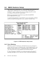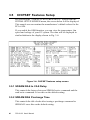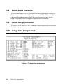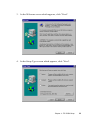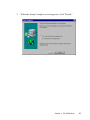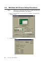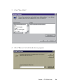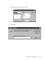
1
PCA-6166
Full-size Super 7 Pentium®
MMX processor-based
PCI/ISA-bus CPU card
Copyright notice
This document is copyrighted, 1999, by Advantech Co., Ltd. All
rights are reserved. Advantech Co., Ltd. reserves the right to make
improvements to the products described in this manual at any time
without notice.
No part of this manual may be reproduced, copied, translated or
transmitted in any form or by any means without the prior written
permission of Advantech Co., Ltd. Information provided in this
manual is intended to be accurate and reliable. However, Advantech
Co., Ltd. assumes no responsibility for its use, nor for any infringements upon the rights of third parties which may result from its
use.
Acknowledgements
• Adaptec and EZ-SCSI are trademarks of Adaptec Inc.
• AWARD is a trademark of AWARD Software, Inc.
• AMD is a trademark of Advanced Micro Devices, Inc.
• IBM and PC are trademarks of International Business Machines
Corporation.
• Intel and Pentium are trademarks of Intel Corporation.
• MS-DOS is a trademark of Microsoft Corporation.
• SiS is a trademark of Silicon Integrated Systems Corporation.
All other product names or trademarks are the properties of their
respective owners.
Part No. 2006616600
1st Edition Printed in Taiwan September 1999
A Message to the Customer
Advantech customer services
Each and every Advantech product is built to the most exacting
specifications to ensure reliable performance in the harsh and
demanding conditions typical of industrial environments. Whether
your new Advantech equipment is destined for the laboratory or the
factory floor, you can be assured that your product will provide the
reliability and ease of operation for which the name Advantech has
come to be known.
Your satisfaction is our primary concern. Here is a guide to
Advantech’s customer services. To ensure you get the full benefit of
our services, please follow the instructions below carefully.
Technical support
We want you to get the maximum performance from your products.
So if you run into technical difficulties, we are here to help. For the
most frequently asked questions, you can easily find answers in your
product documentation. These answers are normally a lot more
detailed than the ones we can give over the phone.
So please consult this manual first. If you still cannot find the answer,
gather all the information or questions that apply to your problem, and
with the product close at hand, call your dealer. Our dealers are well
trained and ready to give you the support you need to get the most
from your Advantech products. In fact, most problems reported are
minor and are able to be easily solved over the phone.
In addition, free technical support is available from Advantech
engineers every business day. We are always ready to give advice on
application requirements or specific information on the installation
and operation of any of our products.
ü
ü
ü
ü
ü
ü
ü
ü
ü
ü
ü
ü
ü
ü
ü
ü
ü
ü
BIOS: Award P&P Flash BIOS
L2 cache: 1 MB
Max. system RAM: 384 MB
(3 x 168-pin DIMM sockets)
ISA High Drive: Up to 64 mA
USB port
2 EIDE connectors
Solid state disk: Supports M-Systems’
DOCfi 2000 Flash disk up to 144 MB
2 serial, 1 parallel ports
VGA: AGP/VGA (built-in on chip)
SCSI: 32-bit PCI Ultra2 SCSI
(Adaptec 7890 chipset)
ü
ü
ü
System chipset: SiS 530
LAN: 10/100Base-T Ethernet
(Intel 82558 chipset)
ü
ü
CPU: Intel Pentiumfi MMX 166 ~ 233 MHz
AMD K6-2, K6-3, 500 MHz and faster
ü
ü
ü
ü
ü
ü
ü
ü
ü
ü
ü
ü
ü
ü
ü
ü
ü
ü
ü
ü
ü
ü
ü
ü
ü
PCA-6166E PCA-6166S PCA-6166F
PCA-6166
Model
PCA-6166 Series comparison table
Product warranty
Advantech warrants to you, the original purchaser, that each of its
products will be free from defects in materials and workmanship for
one year from the date of purchase.
This warranty does not apply to any products which have been
repaired or altered by persons other than repair personnel authorized
by Advantech, or which have been subject to misuse, abuse, accident
or improper installation. Advantech assumes no liability under the
terms of this warranty as a consequence of such events.
If an Advantech product is defective, it will be repaired or replaced at
no charge during the warranty period. For out-of-warranty repairs,
you will be billed according to the cost of replacement materials,
service time and freight. Please consult your dealer for more details.
If you think you have a defective product, follow these steps:
1. Collect all the information about the problem encountered. (For
example, type of PC, CPU speed, Advantech products used, other
hardware and software used, etc.) Note anything abnormal and list
any on-screen messages you get when the problem occurs.
2. Call your dealer and describe the problem. Please have your
manual, product, and any helpful information readily available.
3. If your product is diagnosed as defective, obtain an RMA (return
material authorization) number from your dealer. This allows us to
process your return more quickly.
4. Carefully pack the defective product, a fully-completed Repair and
Replacement Order Card and a photocopy proof of purchase date
(such as your sales receipt) in a shippable container. A product
returned without proof of the purchase date is not eligible for
warranty service.
5. Write the RMA number visibly on the outside of the package and
ship it prepaid to your dealer.
Initial Inspection
Before you begin installing your card, please make sure that the
following materials have been shipped:
• 1 PCA-6166 Pentium® MMX single board computer
• 1CPU, and 1 cooling fan (optional)
• 1 PCA-6166 User's Manual
• Utility disks/CD with VGA BIOS
• IDE disks/CD
• Ethernet driver disks/CD (PCA-6166E/F only)
• SCSI driver disks/CD (PCA-6166S/F only)
• 1 FDD cable
• 2 EIDE HDD cables for ATA66
• 1 printer cable and 1 serial port cable
• 1 ivory cable for keyboard and mouse
• 1 SCSI single-end cable (PCA-6166S/F only)
• 1 USB cable (optional)
• 1 ATX-to-PS/2 power cable
If any of these items are missing or damaged, contact your distributor
or sales representative immediately.
We have carefully inspected the PCA-6166 mechanically and
electrically before shipment. It should be free of marks and scratches
and in perfect working order upon receipt.
As you unpack the PCA-6166, check it for signs of shipping damage.
(For example, damaged box, scratches, dents, etc.) If it is damaged or
it fails to meet the specifications, notify our service department or
your local sales representative immediately. Also notify the carrier.
Retain the shipping carton and packing material for inspection by the
carrier. After inspection, we will make arrangements to repair or
replace the unit.
Contents
Chapter 1 Hardware Configuration .............................. 1
1.1
1.2
1.3
Introduction ........................................................................2
Features ...............................................................................3
Specifications ......................................................................4
1.3.1 System .........................................................................4
1.3.2 Memory .......................................................................4
1.3.3 Input/Output ................................................................4
1.3.4 VGA interface
(PCA-6166/6166E/6166S/6166F only) .......................5
1.3.5 SCSI interface (PCA-6166S/6166F only) ...................5
1.3.6 Ethernet LAN (PCA-6166E/6166F only) ...................5
1.3.7 SSD .............................................................................5
1.3.8 Industrial features .......................................................5
1.3.9 Mechanical and environmental specifications ............5
1.4 Board Layout: Main Features ..........................................6
1.5 Jumpers and Connectors ...................................................7
1.6 Board Layout: Jumper and Connector Locations ..........9
1.7 Safety Precautions ............................................................10
1.8 Jumper Settings ................................................................11
1.8.1 How to set jumpers ...................................................11
1.8.2 CPU clock and frequency ratio setting (SW1) ..........11
1.8.3 Voltage regulator setting (SW2) ............................... 13
1.8.4 CMOS clear (J1) ....................................................... 14
1.8.5 Watchdog timer output (J2) ......................................14
1.8.6 DiskOnChip® 2000 Flash disk address select (J3) ....15
1.9 System Memory ................................................................17
1.9.1 Sample calculation: DIMM memory capacity ..........17
1.9.2 Supplementary information about DIMMs ..............18
1.10 Memory Installation Procedures ....................................19
1.11 CPU Installation ...............................................................20
Chapter 2 Connecting Peripherals ............................ 21
2.1
2.2
2.3
2.4
2.5
2.6
2.7
2.8
2.9
2.10
2.11
2.12
2.13
Primary (CN1) and Secondary (CN2) IDE Connectors 22
Floppy Drive Connector (CN3) .......................................23
Parallel Port Connector (CN4) .......................................23
SCSI Connector (CN5) ....................................................24
USB Connector (CN6) .....................................................25
VGA Connector (CN7) ....................................................25
Ethernet Connector (CN8) ..............................................26
Serial Ports (CN9: COM1; CN10: COM2) .................... 26
PS/2 Keyboard and Mouse Connector (CN11) .............27
External Keyboard Connector (CN12) ..........................27
IR Connector (CN13) ....................................................... 28
CPU Fan Connector (CN14) ........................................... 28
Front Panel Connectors (CN16, CN17, CN18,
CN19 and CN21) ..............................................................29
2.13.1 Keyboard lock and power on LED (CN16) ............29
2.13.2 External speaker (CN17) .........................................29
2.13.3 Reset (CN18)...........................................................29
2.13.4 IDE LED (CN19) ....................................................30
2.13.5 ATX soft power switch (CN21) .............................. 30
2.14 ATX Power Control Connectors (CN20 and CN21) .....30
2.14.1 ATX feature connector (CN20) and soft power .........
switch connector (CN21) ........................................30
2.14.2 Controlling the soft power switch ...........................31
Chapter 3 Award BIOS Setup ..................................... 33
3.1
3.2
3.3
3.4
Introduction ......................................................................34
Entering Setup .................................................................. 34
Standard CMOS Setup ....................................................35
BIOS Features Setup ....................................................... 36
3.4.1 Virus Warning ...........................................................36
3.4.2 Boot Sequence...........................................................37
3.4.3 Boot Up Floppy Seek ................................................37
3.4.4 Boot Up NumLock Status .........................................38
3.4.5 Typematic Rate Setting .............................................38
3.5
3.6
3.7
3.8
3.9
3.4.6 Typematic Rate (Chars/Sec) .....................................38
3.4.7 Typematic Delay (msec) ...........................................38
3.4.8 Security Option .........................................................38
3.4.9 PCI/VGA Palette Snoop............................................39
3.4.10 OS Select for DRAM > 64MB................................39
3.4.11 Video BIOS Shadow ...............................................39
3.4.12 C8000-CBFFF Shadow / DC000-DFFFF Shadow .39
3.4.13 Cyrix 6 x 86/MII CPUID ........................................39
CHIPSET Features Setup ...............................................40
3.5.1 SDRAM RAS to CAS Delay ....................................40
3.5.2 SDRAM RAS Precharge Time .................................40
3.5.3 SDRAM CAS Latency Time ....................................41
3.5.4 DRAM Opt RAS Precharge ......................................41
3.5.5 ISA Bus Clock Frequency.........................................41
3.5.6 Starting point of paging ............................................41
3.5.7 PCI Peer Concurrency ...............................................41
3.5.8 Read Prefetch Memory RD .......................................41
3.5.9 Assert TRDY After Prefet ........................................41
3.5.10 AGP Aperture Size (MB) ........................................42
3.5.11 Memory Hole At 15M-16M ...................................42
3.5.12 PCI Delayed Transaction ........................................42
Power Management Setup ..............................................43
3.6.1 Power Management ..................................................43
3.6.2 HDD Power Down ....................................................43
3.6.3 Soft-Off by PWR-BTTN ...........................................44
3.6.4 HDD Ports Activity ...................................................44
PCI Configuration Setup .................................................44
3.7.1 Resources Controlled By ..........................................45
3.7.2 Reset Configuration Data ..........................................45
3.7.3 IRQ-xx assigned to : PCI/ISA PnP ...........................45
3.7.4 PCI IRQ Activated by ...............................................45
Load BIOS Defaults .........................................................46
Load Setup Defaults .........................................................46
3.10 Integrated Peripherals .....................................................46
3.10.1 IDE Primary Master/Slave PIO/UDMA Mode,
IDE Secondary Master/Slave PIO/UDMA Mode (Auto) 47
3.10.2 IDE Burst Mode ......................................................47
3.10.3 IDE Data Port Post Write ........................................47
3.10.4 IDE HDD Block Mode ...........................................47
3.10.5 Onboard FDC Controller ........................................47
3.10.6 Onboard Serial Port 1 (3F8H/IRQ4) .......................47
3.10.7 Onboard Serial Port 2 (2F8H/IRQ3) .......................48
3.10.8 Onboard Parallel Port (378H/IRQ7) .......................48
3.10.9 Parallel Port Mode (ECP + EPP) ............................48
3.10.10 ECP Mode Use DMA ...........................................48
3.11 Password Setting ..............................................................49
3.12 IDE HDD Auto Detection ................................................49
3.13 Save & Exit Setup ............................................................50
3.14 Exit Without Saving .........................................................50
Chapter 4 PCI SVGA Setup......................................... 51
4.1
4.2
4.3
4.4
Before You Begin .............................................................52
Driver Installation ............................................................53
Windows 95/98 Drivers Setup Procedure ......................54
Windows NT Drivers Setup Procedure ..........................58
Chapter 5 LAN Configuration ..................................... 63
5.1
5.2
5.3
5.4
5.5
5.6
Introduction ......................................................................64
Features .............................................................................64
Driver Installation ............................................................65
Windows 95 Drivers Setup Procedure ...........................66
Windows 98 Drivers Setup Procedure ...........................72
Windows NT Drivers Setup Procedure ..........................73
Chapter 6 SCSI Setup and Configurations................ 77
6.1
6.2
6.3
Introduction ......................................................................78
Configuring the SCSI Adapter .......................................78
SCSI Terminators ............................................................79
6.4
Adaptec EZ-SCSI Utility .................................................80
6.4.1 Quick start instructions .............................................80
6.4.2 DOS ...........................................................................80
6.4.3 SCSI device troubleshooting.....................................80
6.4.4 DOS device drivers ...................................................81
6.4.5 DOS ASPI managers .................................................81
6.4.6 DOS formatting utilities............................................ 82
Chapter 7 SiS IDE Driver Installation ......................... 85
7.1
7.2
Installation for Windows 95 and 98 ............................... 86
Installation for Windows NT 4.0 ....................................87
Chapter 8 On-board Security Setup .......................... 89
8.1
8.2
Introduction ......................................................................90
Driver Installation ............................................................90
8.2.1 Necessary prerequisites .............................................90
8.2.2 Before you begin ....................................................... 90
8.2.3 Windows 98 drivers setup procedure ........................91
Appendix A Programming the Watchdog Timer ....... 99
A.1
Programming the Watchdog Timer .............................100
Appendix B Pin Assignments .................................. 103
B.1
B.2
B.3
B.4
B.5
B.6
B.7
B.8
B.9
B.10
B.11
B.12
B.13
B.14
B.15
B.16
B.17
B.18
B.19
B.20
B.21
B.22
IDE Hard Drive Connector (CN1, CN2) ......................104
Floppy Drive Connector (CN3) .....................................105
Parallel Port Connector (CN4) .....................................106
SCSI Connector (CN5) ..................................................107
USB Connector (CN6) ...................................................108
VGA Connector (CN7) ..................................................108
Ethernet 10/100Base-T RJ-45 Connector (CN8) .........109
COM1/COM2 RS-232 Serial Port (CN9, CN10) ........109
Keyboard and Mouse Connnector (CN11) .................. 110
External Keyboard Connector (CN12) ........................110
IR Connector (CN13) .....................................................111
CPU Fan Power Connector (CN14) .............................111
Power LED and Keylock Connector (CN16) ...............112
External Speaker Connector (CN17) ...........................112
Reset Connector (CN18) ................................................113
HDD LED Connector (CN19) .......................................113
ATX Feature Connector (CN20) ..................................113
System I/O Ports ............................................................114
DMA Channel Assignments .......................................... 115
Interrupt Assignments ...................................................115
1st MB Memory Map.....................................................116
PCI Bus Map .................................................................. 116
Appendix C DiskOnChip® 2000 Installation Guide . 117
C.1
DiskOnChip® 2000 Quick Installation Guide ..............118
C.1.1 DiskOnChip® 2000 installation instructions ..........118
C.1.2 Addtional information and assistance ....................119
CHAPTER
1
Hardware Configuration
This chapter gives background information on the PCA-6166. It then shows you
how to configure the card to match your
application and prepare it for installation
into your PC.
Sections include:
• Introduction
• Features
• Specifications
• Board Layout
• Jumpers and Connectors
• Safety Precautions
• Jumper Settings
• System Memory
• Memory Installation Procedures
• Cache Memory
• CPU Installation
1.1
Introduction
The PCA-6166 Series all-in-one industrial grade CPU card can use
the Intel® Pentium® MMX, AMD K6-2 or K6-3 processors. It also
uses the SiS530 AGP chipset. The card works with standard ISA or
PCI/ISA-bus passive backplanes.
The CPU provides 1 MB L2 cache on board. It has two PCI EIDE
interfaces (for up to four devices) and a floppy disk drive interface
(for up to two devices). Other features include two RS-232 serial
ports (16C550 UARTs with 16-byte FIFO or compatible), one
enhanced parallel port (supports SPP/EPP/ECP) and one USB
(Universal Serial Bus) port. The PCI enhanced IDE controller
supports Ultra DMA/33/66 and PIO Mode 4 operation. This provides
data transfer rates of over 66 MB/sec. System BIOS supports boot-up
from an IDE CD-ROM, SCSI CD-ROM, ZIP, and LS-120.
A backup of CMOS data is stored in the Flash memory, which
protects data even after a battery failure. Also included is a 63-level
watchdog timer, which resets the CPU or generates an interrupt if a
program cannot be executed normally. This enables reliable operation
in unattended environments.
The PCA-6166 series offers several impressive industrial features
such as a built-in VGA (AGP), a PCI Ultra2 SCSI controller, a
10/100Base-T networking controller, three DIMM slots for a total of
384 MB RAM memory, and an ISA High Drive. In addition, the
PCA-6166 series supports a solid state disk (SSD) using M-Systems
Corporation's DiskOnChip® 2000 Flash disk, for up to 144 MB of
non-volatile, reliable memory that is not vulnerable to the hazards of
an industrial computing environment. All these make it an ideal
choice for applications that require both high performance and full
functionality.
Note:
2
Some of the features mentioned above are not
available with all models. For more information about
the specifications of a particular model, see Section
1.3 Specifications.
PCA-6166 User's Manual
1.2
Features
• Socket 7 architecture
• Accepts Intel Pentium® MMX processors up to 233 MHz, AMD
K6-2, K6-3, 500 MHz or faster
• SiS530 AGP set, FSB 66/100 MHz
• Three DIMM sockets to support Intel PC100-compliant SDRAMs
up to 384 MB
• Award Plug and Play Flash BIOS, 2 Mbit
• Built-in AGP/VGA (on SiS 530)
• On-board Ethernet (PCA-6166E/F only)
• On-board SCSI (PCA-6166S/F only)
• Supports DOC® 2000
• On-board ATX power control connector to meet ACPI requirements
• Two enhanced IDE ports, supporting Ultra DMA/66, PIO Mode 4
(BIOS enabled/disabled)
• Two USB ports
• Two RS-232 serial ports
• One bidirectional parallel port, supports ECP/EPP/SPP
• One floppy port and one keyboard/mouse port
• PCI V2.1 compliant
• PICMG 2.0 compliant
• CMOS backup battery life of 7 years
• HISA (ISA High Drive) up to 64 mA
Chapter 1 Hardware Configuration
3
1.3
Specifications
1.3.1 System
• CPU: Intel® Pentium® MMX processors up to 233 MHz, AMD
K6-2, K6-3, up to 500 MHz and faster
• L2 cache: 1 MB on board
• BIOS: Award Flash BIOS, 2 Mbit
• Green function: Supports power management operation via BIOS.
Activated by keyboard or mouse activity
• PCI enhanced IDE hard disk drive interface: Supports up to four
IDE (AT-bus) large hard disk drives or other enhanced IDE
devices. Supports PIO Mode 4 (16.67 MB/s data transfer rate) and
Ultra DMA/66 (66 MB/s data transfer rate). BIOS enabled/disabled
• Floppy disk drive interface: Supports up to two floppy disk drives,
5¼" (360 KB and 1.2 MB) and/or 3½" (720 KB, 1.44 MB, and 2.88
MB). BIOS enabled/disabled
1.3.2 Memory
• RAM: Up to 384 MB in three available 168-pin DIMM sockets.
Supports PC100-compliant SDRAMs
1.3.3 Input/Output
• Bus interface: PCI/ISA bus, PICMG compliant
• Enhanced parallel port: Configurable to LPT1, LPT2, LPT3 or
disabled. Standard DB-25 female connector provided. Supports
EPP/ECP/SPP
• Serial ports: Two RS-232 ports with 16C550 UARTs (or
compatible) with 16-byte FIFO buffer. Supports speeds up to 115.2
Kbps. Ports can be individually configured to COM1, COM2 or
disabled
• Keyboard and PS/2 mouse connector: A 6-pin mini-DIN
connector is located on the mounting bracket for easy connection to
a keyboard or PS/2 mouse. An on-board keyboard pin header
connector is also available
• ISA driver current: 64 mA (High Drive)
4
PCA-6166 User's Manual
1.3.4 VGA interface (PCA-6166/6166E/6166S/6166F only)
• Supports AGP 2X, 133 MHz
• Controller: SiS530 built-in VGA (AGP)
• Display memory: Share system memory area 2/4/8 MB
1.3.5 SCSI interface (PCA-6166S/6166F only)
• PCI SCSI: Supports 32-bit PCI interface and Ultra2 SCSI or legacy
single-ended devices; data transfer up to 80 MB/sec.
• Chipset: Adaptec AI C 7890
1.3.6 Ethernet LAN (PCA-6166E/6166F only)
• Supports 10/100Base-T Ethernet networking
• Chipset: Intel® 82558
1.3.7 SSD
• Supports M-Systems' DiskOnChip® 2000 Flash disk up to 144 MB
1.3.8 Industrial features
• Watchdog timer: Can generate a system reset or IRQ11. The watchdog timer is programmable, with each unit equal to one second (63
levels). The program uses I/O port hex 443h to control the watchdog
timer
1.3.9 Mechanical and environmental specifications
•
•
•
•
•
Operating temperature: 0 ~ 60° C (32 ~ 140° F)
Storage temperature: -40 ~ 60° C (-40 ~ 140° F)
Humidity: 20 ~ 95% non-condensing
Power supply voltage: +5 V, ±12 V
Power consumption:
+5 V @ 5.59 A (for Pentium® MMX 233 MHz)
+5 V @ 6.08 A (for AMD K6-2 400 MHz)
+5 V @ 7.83 A (for AMD K6-3 450 MHz)
• Board size: 338 x 122 mm (13.3" x 4.8")
• Board weight: 0.5 kg (1.2 lbs)
Chapter 1 Hardware Configuration
5
6
EIDE connectors
CPU ZIF Socket 7
SiS530 chipset
PCA-6166 User's Manual
Intel 82558
COM2
DOC® 2000
FDD connector
Parallel port
SCSI connector
Adaptec 7890
3 DIMM modules
(up to 1.5 GB)
PS/2 mouse and
keyboard connector
COM1
LAN connector
VGA connector
USB port
1.4
Board Layout: Main Features
Figure 1-1: Board layout: main features
1.5
Jumpers and Connectors
Connectors on the PCA-6166 board link it to external devices such as
hard disk drives and a keyboard. In addition, the board has a number
of jumpers used to configure your system for your application.
The tables below list the function of each of the board jumpers and
connectors. Later sections in this chapter give instructions on setting
jumpers. Chapter 2 gives instructions for connecting external devices
to your card.
Table 1-1: Jumpers
Label
Function
J1
CMOS clear
J2
Watchdog timer output
J3
DiskOnChip® 2000 address setting
SW1
CPU clock and frequency ratio setting
SW2
Voltage regulator setting
Chapter 1 Hardware Configuration
7
Table 1-2: Connectors
8
Label
Function
CN1
Primary IDE connector
CN2
Secondary IDE connector
CN3
Floppy drive connector
CN4
Parallel port
CN5
SCSI connector
CN6
USB port
CN7
VGA connector
CN8
10/100Base-T Ethernet connector
CN9
Serial port: COM1
CN10
Serial port: COM2
CN11
PS/2 keyboard and mouse
CN12
External keyboard connector
CN13
Infrared (IR) connector
CN14
CPU fan connector
CN16
Keyboard lock and power LED
CN17
External speaker
CN18
Reset connector
CN19
IDE LED
CN20
ATX feature connector
CN21
ATX soft power switch
CN22
ACPI LED connector (reserved)
PCA-6166 User's Manual
1.6
Board Layout: Jumper and Connector
Locations
Figure 1-2: Board layout: jumper and connecter locations
Chapter 1 Hardware Configuration
9
1.7
Safety Precautions
Warning! Always completely disconnect the power cord from
your chassis whenever you work with the hardware.
Do not make connections while the power is on.
Sensitive electronic components can be damaged by
sudden power surges. Only experienced
electronics personnel should open the PC chassis.
Caution!
10
Always ground yourself to remove any static charge
before touching the CPU card. Modern electronic
devices are very sensitive to static electric charges.
As a safety precaution, use a grounding wrist strap
at all times. Place all electronic components in a
static-dissipative surface or static-shielded bag when
they are not in the chassis.
PCA-6166 User's Manual
1.8
Jumper Settings
This section provides instructions on how to configure your card by
setting jumpers. It also includes the card's default settings and your
options for each jumper.
1.8.1 How to set jumpers
You configure your card to match the needs of your application by
setting jumpers. A jumper is the simplest kind of electric switch. It
consists of two metal pins and a small metal clip (often protected by a
plastic cover) that slides over the pins to connect them. To “close” (or
turn ON) a jumper, you connect the pins with the clip. To “open” (or
turn OFF) a jumper, you remove the clip. Sometimes a jumper
consists of a set of three pins, labeled 1, 2 and 3. In this case you
connect either pins 1 and 2, or 2 and 3.
A pair of needle-nose pliers may be useful when setting jumpers.
1.8.2 CPU clock and frequency ratio setting (SW1)
You must configure your PCA-6166 CPU card to the frequency of
your processor by setting jumper SW1. The PCA-6166 SW1 jumper is
equipped to use Intel® Pentium® MMX, AMD K6-2 and K6-3
processors. Configure your PCA-6166 as follows:
Chapter 1 Hardware Configuration
11
Table 1-3: CPU clock and frequency ratio setting (SW1)
Freq.
(MHz)
Multiplication
Bus freq.
(MHz)
SW1-1
AMD-K6-III/450
450
4.5x
100
AMD-K6-III/400
400
4.0x
100
AMD-K6-2/366
366
5.5x
AMD-K6-2/350
350
3.5x
AMD-K6-2/333
333
5.0x
AMD-K6-2/300
300
3.0x
AMD-K6-2/300
300
4.5x
66
AMD-K6-2/266
266
4.0x
AMD-K6/300
300
4.5x
AMD-K6/266
266
4.0x
AMD-K6/233
233
AMD-K6/200
200
AMD-K6/166
SW1-2
SW1-3
SW1-4
SW1-5
SW1-6
ON
ON
ON
OFF
ON
ON
ON
OFF
ON
OFF
ON
ON
66
OFF
OFF
ON
ON
ON
ON
100
OFF
OFF
OFF
OFF
ON
ON
66
OFF
ON
ON
ON
ON
ON
100
OFF
ON
OFF
OFF
ON
ON
ON
ON
ON
ON
ON
ON
66
ON
OFF
ON
ON
ON
ON
66
ON
ON
ON
ON
ON
ON
66
ON
OFF
ON
ON
ON
ON
3.5x
66
OFF
OFF
OFF
ON
ON
ON
3.0x
66
OFF
ON
OFF
ON
ON
ON
166
2.5x
66
ON
ON
OFF
ON
ON
ON
AMD-K5/133
100
1.5x
66
OFF
OFF
OFF
ON
ON
ON
AMD-K5/100
100
1.5x
66
OFF
OFF
OFF
ON
ON
ON
Intelfi Pentiumfi P54C
166
2.5x
66
ON
ON
OFF
ON
ON
ON
Intel Pentium P54C
133
2.0x
66
ON
OFF
OFF
ON
ON
ON
Intelfi Pentiumfi P54C
100
1.5x
66
OFF
OFF
OFF
ON
ON
ON
Intelfi Pentiumfi P55C
233
3.5x
66
OFF
OFF
OFF
ON
ON
ON
Intel Pentium P55C
200
3.0x
66
OFF
ON
OFF
ON
ON
ON
Intelfi Pentiumfi P55C
166
2.5x
66
ON
ON
OFF
ON
ON
ON
CPU Model
fi
fi
12
fi
fi
PCA-6166 User's Manual
1.8.3 Voltage regulator setting (SW2)
These jumpers set the VCORE voltage supplied to the CPU. Switching
regulators allow some jumper settings to be the same for two voltages
of different power planes.
Table 1-4: CPU V CORE voltage selection
V CC-CORE
SW2-1
VID0
1.80
OFF
ON
OFF
ON
ON
1.85
ON
ON
OFF
ON
ON
1.90
OFF
OFF
ON
ON
ON
1.95
ON
OFF
ON
ON
ON
2.00
OFF
ON
ON
ON
ON
2.05
ON
ON
ON
ON
ON
No core
OFF
OFF
OFF
OFF
OFF
2.1
ON
OFF
OFF
OFF
OFF
2.2
OFF
ON
OFF
OFF
OFF
2.3
ON
ON
OFF
OFF
OFF
2.4
OFF
OFF
ON
OFF
OFF
2.5
ON
OFF
ON
OFF
OFF
2.6
OFF
ON
ON
OFF
OFF
2.7
ON
ON
ON
OFF
OFF
2.8
OFF
OFF
OFF
ON
OFF
2.9
ON
OFF
OFF
ON
OFF
3.0
OFF
ON
OFF
ON
OFF
3.1
ON
ON
OFF
ON
OFF
3.2
OFF
OFF
ON
ON
OFF
3.3
ON
OFF
ON
ON
OFF
3.4
OFF
ON
ON
ON
OFF
3.5
ON
ON
ON
ON
OFF
Note:
SW2-2
VID1
SW2-3
VID2
SW2-4
VID3
SW2-5
VID4
SW2-6 should be set as OFF. If you are using a
Cyrix CPU, you must set SW2-6 as ON.
Chapter 1 Hardware Configuration
13
1.8.4 CMOS clear (J1)
The PCA-6166 CPU card contains a jumper that can erase CMOS data
and reset the system BIOS information. Normally this jumper should
be set with pins 1-2 closed. If you want to reset the CMOS data, set J1
to 2-3 closed for just a few seconds, and then move the jumper back to
1-2 closed. This procedure will reset the CMOS to its default setting.
Table 1-5: CMOS clear (J1)
Function
Jumper setting
* Keep CMOS data
1-2 closed
Clear CMOS data
2-3 closed
1
1
* default setting
1.8.5 Watchdog timer output (J2)
The PCA-6168 contains a watchdog timer that will reset the CPU or
send a signal to IRQ11 in the event the CPU stops processing. This
feature means the PCA-6166 will recover from a software failure or an
EMI problem. The J2 jumper settings control the outcome of what the
computer will do in the event the watchdog timer is tripped.
Table 1-6: Watchdog timer output (J2)
Function
Jumper setting
IRQ11
1-2 closed
* Reset
2-3 closed
1
1
* default setting
14
PCA-6166 User's Manual
1.8.6 DiskOnChip® 2000 Flash disk address select (J3)
The PCA-6166 includes a 32-pin socket for M-Systems' DiskOnChip®
2000 Flash disk module. This revolutionary solid state disk enables
critical system information to be stored within an on-board Flash disk
for virtually instantaneous data access.
You must specify the memory address you want to use for your
DiskOnChip 2000 Flash disk module by setting jumper (J3). Available settings are as follows:
Chapter 1 Hardware Configuration
15
Table 1-7: DiskOnChip® 2000 Flash disk memory address jumper settings (J3)
16
Segment
A
B
C
C800h
ON
ON
ON
CC00h
ON
ON
OFF
D000h
ON
OFF
ON
D400h
ON
OFF
OFF
D800h
OFF
ON
ON
DC00h
OFF
ON
OFF
E000h
OFF
OFF
ON
Disable
OFF
OFF
OFF
PCA-6166 User's Manual
A
B
C
A
B
C
A
B
C
A
B
C
A
B
C
A
B
C
A
B
C
A
B
C
1.9
System Memory
The top-left edge of the PCA-6166 contains three sockets for 168-pin
dual inline memory modules (DIMMs). All three sockets use 3.3 V
unbuffered synchronous DRAMs (SDRAM). DIMMs are available in
capacities of 16, 32, 64, or 128 MB. The sockets can be filled in any
combination with DIMMs of any size, giving your PCA-6166 single
board computer between 16 MB and 384 MB of memory. Use the
following table to calculate the total DRAM memory within your
computer:
Table 1-8: DIMM module allocation table
Socket number
168-pin DIMM memory
1
(16, 32, 64, or 128 MB) x 1
2
(16, 32, 64, or 128 MB) x 1
3
(16, 32, 64, or 128 MB) x 1
1.9.1 Sample calculation: DIMM memory capacity
Suppose you install a 128 MB DIMM into your PCA-6166's socket 1
and a 32 MB DIMM into sockets 2 and 3. Your total system memory
is 192 MB, calculated as follows:
Table 1-9: DIMM memory capacity sample calculation
Socket number
168-pin
DIMM memory
Total memory
1
128 MB
x1
128 MB
2
32 MB
x1
32 MB
3
32 MB
x1
32 MB
Total memory
192 MB
Chapter 1 Hardware Configuration
17
1.9.2 Supplementary information about DIMMs
Your PCA-6166 can accept SDRAM memory chips (with or without
parity). Also note:
• If the PCA-6166 operates at 100 MHz, only use PC100-compliant
DIMMs. Most systems will not even boot if non-compliant modules
are used. This is due to strict timing issues involved at this speed.
• SDRAM chips are usually thinner and have higher pin density than
EDO chips.
• Chips with 9 chips/side support ECC; chips with 8 chips/side do not
support ECC.
• Single-sided modules are typically 16, 32, 64 or 128 MB;
double-sided modules are usually 32, 64, 128, or 256 MB.
18
PCA-6166 User's Manual
1.10 Memory Installation Procedures
To install DIMMs, first make sure the two handles of the DIMM
socket are in the "open" position. i.e. The handles lean outward.
Slowly slide the DIMM module along the plastic guides on both ends
of the socket. Then press the DIMM module right down into the
socket, until you hear a click. This is when the two handles have
automatically locked the memory module into the correct position of
the DIMM socket (see Figure 1-3, DIMM installation). To remove the
memory module, just push both handles outward, and the memory
module will be ejected by the mechanism in the socket.
Figure 1-3: DIMM installation
Important: You must install SDRAM progressively from BANK0
through BANK2 on DIMM socket, otherwise the
system will not work.
Chapter 1 Hardware Configuration
19
1.11 CPU Installation
The PCA-6166 provides a socket 7 for easy CPU installation. The
CPU on the board must have a fan or heat sink attached, to prevent
overheating.
Warning:
Without a fan or heat sink, the CPU will overheat
and cause damage to both the CPU and the motherboard.
To install a CPU, first turn off your system and remove its cover.
Locate the processor socket 7.
1. Make sure the socket 7 lever is in the upright position. To raise the
lever, pull it out to the side a little and raise it as far as it will go.
2. Place the CPU in the empty socket. Follow the instructions that
came with the CPU. If you have no instructions, complete the
following procedure. Carefully align the CPU so it is parallel to
the socket and the notch on the corner of the CPU corresponds
with the notches on the inside of the socket. Gently slide the CPU
in. It should insert easily. If it does not insert easily, pull the lever
up a little bit more.
3. Press the lever down. The plate will slide forward. You will feel
some resistance as the pressure starts to secure the CPU in the
socket. This is normal and will not damage the CPU.
When the CPU is installed, the lever should snap into place at the side
of the socket.
Note:
To remove a CPU, pull the lever out to the side a
little and raise it as far as it will go. Lift out the CPU.
When you install a new CPU, be sure to adjust the board settings,
such as CPU type and CPU clock. Improper settings may damage
the CPU.
20
PCA-6166 User's Manual
CHAPTER
2
Connecting Peripherals
This chapter tells how to connect peripherals, switches and indicators to the
PCA-6166 board. You can access most of
the connectors from the top of the board
while it is installed in the chassis. If you
have a number of cards installed, or your
chassis is very tight, you may need to
partially remove the card to make all the
connections.
2.1
Primary (CN1) and Secondary (CN2) IDE
Connectors
You can attach up to four IDE (Integrated Device Electronics) drives
to the PCA-6166’s internal controller. The primary (CN1) and
secondary (CN2) connectors can each accommodate two drives.
Wire number 1 on the cable is red or blue and the other wires are
gray. Connect one end to connector CN1 or CN2 on the CPU card.
Make sure that the red/blue wire corresponds to pin 1 on the connector (in the upper right hand corner). See Chapter 1: Hardware
Configuration for help finding the connector. Note that pin 20 has
been removed. This ensures that ribbon cables will be connected with
the correct orientation.
Unlike floppy drives, IDE hard drives can connect in either position
on the cable. If you install two drives to a single connector, you will
need to set one as the master and one as the slave. You do this by
setting the jumpers on the drives. If you use just one drive per
connector, you should set each drive as the master. See the documentation that came with your drive for more information.
Connect the first hard drive to the other end of the cable. Wire 1 on
the cable should also connect to pin 1 on the hard drive connector,
which is labeled on the drive circuit board. Check the documentation
that came with the drive for more information.
Connect the second hard drive to the remaining connector (CN2 or
CN1), in the same way as described above.
Important: Ultra DMA/66 devices must use a 40-pin with
80-conductor cable.
22
PCA-6166 User's Manual
2.2
Floppy Drive Connector (CN3)
You can attach up to two floppy disk drives to the PCA-6166's
on-board controller. You can use any combination of 5.25"
(360 KB / 1.2 MB) and/or 3.5" (720 KB / 1.44 MB / 2.88 MB) drives.
The card comes with a 34-pin daisy-chain drive connector cable. On
one end of the cable is a 34-pin flat-cable connector. On the other end
are two sets of floppy disk drive connectors. Each set consists of a
34-pin flat-cable connector (usually used for 3.5" drives) and a
printed circuit-board connector (usually used for 5.25" drives). You
can use only one connector in each set. The set on the end (after the
twist in the cable) connects to the A: floppy drive. The set in the
middle connects to the B: floppy drive.
2.3
Parallel Port Connector (CN4)
The parallel port is normally used to connect the CPU card to a
printer. The PCA-6166 includes an on-board parallel port, accessed
through a 26-pin flat-cable connector, CN4. The card comes with an
adapter cable which lets you use a traditional DB-25 connector. The
cable has a 26-pin connector on one end and a DB-25 connector on
the other, mounted on a retaining bracket. The bracket installs at the
end of an empty slot in your chassis, giving you access to the connector.
The parallel port is designated as LPT1, and can be disabled or
changed to LPT2 or LPT3 in the system BIOS setup.
Chapter 2 Connecting Peripherals
23
To install the bracket, find an empty slot in your chassis. Unscrew the
plate that covers the end of the slot. Screw in the bracket in place of
the plate. Next, attach the flat-cable connector to CN4 on the CPU
card. Wire 1 of the cable is red or blue, and the other wires are gray.
Make sure that wire 1 corresponds to pin 1 of CN4. Pin 1 is on the
upper right side of CN4.
2.4
SCSI Connector (CN5)
Note:
Only the PCA-6166S/6166F models contain a SCSI
connector.
The PCA-6166S/F series has a 68-pin, dual in-line connector for
Ultra2 SCSI devices. Connection of SCSI devices requires special
attention, especially when determining the last drive on the SCSI
chain. Refer to Chapter 6 and your device's operating manual for
detailed installation advice.
24
PCA-6166 User's Manual
2.5
USB Connector (CN6)
The PCA-6166 CPU card provides one USB (Universal Serial Bus)
interface, which gives complete Plug & Play and hot attach/detach for
up to 127 external devices.The USB interface complies with USB
Specification Rev. 1.0, and is fuse-protected.
The USB interface is accessed through a 10-pin flat-cable connector,
CN6. The adapter cable has a 10-pin connector on one end and a USB
connector on the bracket.
The USB interface can be disabled in the system BIOS setup.
2.6
VGA Connector (CN7)
The PCA-6166 series includes a PCI SVGA interface that can drive
conventional CRT displays. CN7 is a standard 15-pin D-SUB connector commonly used for VGA. Pin assignments for CRT connector
CN7 are detailed in Appendix B: Pin Assignments.
Chapter 2 Connecting Peripherals
25
2.7
Ethernet Connector (CN8)
Note:
Only the PCA-6166E/6166F models include a
10/100Base-T Ethernet connector.
The PCA-6166E/F is equipped with a high performance 32-bit
PCI-bus Ethernet interface, which is fully compliant with IEEE
802.3/u 10/100 Mbps CSMA/CD standards. It is supported by all
major network operating systems, and is 100% Novell NE-2000
compatible. An on-board RJ-45 jack provides convenient
10/100Base-T RJ-45 operation.
2.8
Serial Ports (CN9: COM1; CN10: COM2)
The PCA-6166 offers two serial ports, CN9 as COM1 and CN10 as
COM2. These ports can connect to serial devices (such as a mouse,
printers, and so on) or to a communication network.
Table 2-1: Serial port connections (COM1, COM2)
Connector
Ports
Address
Interrupt
CN9
COM1
3F8*, 3E8
IRQ4
CN10
COM2
2F8*, 2E8
IRQ3
* default settings
26
PCA-6166 User's Manual
The IRQ and address ranges for both ports are fixed. However, if you
want to disable the port or change these parameters later, you can do
this in the system BIOS setup.
Different devices implement the RS-232 standard in different ways. If
you are having problems with a serial device, be sure to check the pin
assignments for the connector.
2.9
PS/2 Keyboard and Mouse Connector
(CN11)
The PCA-6166 board provides a keyboard connector. A 6-pin
mini-DIN connector (CN11) on the card mounting bracket supports
single-board computer applications. The card comes with an adapter
to convert from the 6-pin mini-DIN connector to a standard DIN
connector and to a PS/2 mouse connector.
2.10 External Keyboard Connector (CN12)
In addition to the PS/2 mouse/keyboard connector on the PCA-6166's
rear plate, there is also an extra on-board external keyboard connector.
This gives system integrators greater flexibility in designing their
systems.
Chapter 2 Connecting Peripherals
27
2.11 IR Connector (CN13)
This connector supports the optional wireless infrared transmitting
and receiving module. This module mounts on the system case. You
must configure the setting through the BIOS setup (see Chapter 3:
Award BIOS Setup).
2.12 CPU Fan Connector (CN14)
This connector supports cooling fans of 500 mA (6 W) or less.
28
PCA-6166 User's Manual
2.13 Front Panel Connectors (CN16, CN17,
CN18, CN19 and CN21)
There are several external switches to monitor and control the
PCA-6166.
2.13.1 Keyboard lock and power on LED (CN16)
CN16 is a 5-pin connector for the keyboard lock and power on LED.
Refer to Appendix B: Pin Assignments for detailed information on
the pin assignments. If a PS/2 or ATX power supply is used, the
system's power LED status will be as indicated below:
Table 2-2: PS/2 or ATX power supply LED status
Power mode
LED (PS/2 power)
LED (ATX power)
System On
On
On
System Suspend
Fast flashes
Fast flashes
System Off
Off
Slow flashes
2.13.2 External speaker (CN17)
CN17 is a 4-pin connector for an extenal speaker. If there is no
external speaker, the PCA-6166 provides an on-board buzzer as an
alternative. To enable the buzzer, set pins 3-4 as closed.
2.13.3 Reset (CN18)
Many computer cases offer the convenience of a reset button. Connect
the wire from the reset button to CN18.
Chapter 2 Connecting Peripherals
29
2.13.4 IDE LED (CN19)
You can connect an LED to connector CN19 to indicate when the
HDD is active.
2.13.5 ATX soft power switch (CN21)
If your computer case is equipped with an ATX power supply, you
should connect the power on/off button on your computer case to
CN21. This connection enables you to turn your computer on and off.
2.14 ATX Power Control Connectors (CN20
and CN21)
Note:
Refer to the diagram on the previous page for the
location of CN21.
2.14.1 ATX feature connector (CN20) and soft power switch
connector (CN21)
The PCA-6166 can support an advanced soft power switch function if
an ATX power supply is used. To enable the soft power switch
function:
1. Take the specially designed ATX-to-PS/2 power cable out of the
PCA-6166's accessory bag.
2. Connect the 3-pin plug of the cable to CN20 (ATX feature
connector).
3. Connect the power on/off button to CN21. (A momentary type of
button should be used.)
Important: If you will not be using an ATX power connector,
make sure that pins 2-3 are closed. Otherwise, the
LAN function will not work.
30
PCA-6166 User's Manual
Warnings: 1. Make sure that you unplug your power supply
when adding or removing expansion cards or other
system components. Failure to do so may cause
severe damage to both your CPU card and expansion cards.
2. ATX power supplies may power on if certain
motherboard components or connections are
touched by metallic objects.
Important: Make sure that the ATX power supply can take at
least a 720 mA load on the 5 V standby lead (5VSB).
If not, you may have difficulty powering on your
system and/or supporting the "Wake on LAN"
function.
2.14.2 Controlling the soft power switch
Users can also identify the current power mode through the system's
power LED (see Section 2.14.1).
Chapter 2 Connecting Peripherals
31
32
PCA-6166 User's Manual
CHAPTER
3
Award BIOS Setup
This chapter describes how to set the
card’s BIOS configuration data.
3.1
Introduction
Award’s BIOS ROM has a built-in setup program that allows users to
modify the basic system configuration. This type of information is
stored in battery-backed RAM so that it retains the setup information
when the power is turned off.
3.2
Entering Setup
Turn on the computer and check for the “patch code”. If there is a
number assigned to the patch code, it means that the BIOS supports
your CPU.
If there is no number assigned to the patch code, please contact
Advantech’s applications engineer to obtain an up-to-date patch code
file. This will ensure that your CPU’s system status is valid.
After ensuring that you have a number assigned to the patch code,
press <Del> to allow you to enter the setup.
Figure 3-1: Award BIOS Setup initial screen
34
PCA-6166 User’s Manual
3.3
Standard CMOS Setup
Choose the “STANDARD CMOS SETUP” option from the “INITIAL
SETUP SCREEN” menu, and the screen below will be displayed. This
standard setup menu allows users to configure system components
such as date, time, hard disk drive, floppy drive, display, and memory.
Figure 3-2: Standard CMOS Setup screen
Chapter 3 Award BIOS Setup
35
3.4
BIOS Features Setup
The “BIOS FEATURES SETUP” screen appears when choosing the
“BIOS FEATURES SETUP” item from the “CMOS SETUP
UTILITY” menu. It allows the user to configure the PCA-6166
according to his particular requirements.
Below are some major items that are provided in the BIOS
FEATURES SETUP screen.
A quick booting function is provided for your convenience. Simply
enable the Quick Booting item to save yourself valuable time.
Figure 3-3: BIOS features setup screen
3.4.1 Virus Warning
While the system is booting up, and after boot-up, any attempt to
write to the boot sector or partition table of the hard disk drive will
halt the system. In this case, a warning message will be displayed.
You can run the anti-virus program to locate the problem.
If Virus Warning is disabled, no warning message will appear if
anything attempts to access the boot sector or hard disk partition.
36
PCA-6166 User’s Manual
3.4.2 Boot Sequence
This function determines the sequence in which the computer will
search the drives for the disk operating system (i.e. DOS). The BIOS
provides the folllowing boot sequences:
A,C, SCSI
C,A, SCSI (Default)
C, CDROM, A
CDROM, C, A
D, A, SCSI
E, A, SCSI
F, A, SCSI
SCSI, A, C
SCSI, C, A
C only
LS/ZIP, C
3.4.3 Boot Up Floppy Seek
During Power-On Self Test (POST), BIOS will determine if the
floppy disk drive installed is 40 or 80 tracks. A 360 KB type drive is
40 tracks; while 720 KB, 1.2 MB, and 1.44 MB type drives are all 80
tracks.
Enabled
BIOS searches the floppy drive to determine if it is 40 or
80 tracks. Note that BIOS cannot differentiate 720 KB, 1.2
MB, and 1.44 MB type drives. This is because they are all
80 tracks.
Disabled BIOS will not search for the floppy drive type by track
number. Note that there will not be any warning message if
the drive installed is 360 KB.
Chapter 3 Award BIOS Setup
37
3.4.4 Boot Up NumLock Status
The default is “On”.
On
Keypad boots up to number keys.
Off
Keypad boots up to arrow keys.
3.4.5 Typematic Rate Setting
The typematic rate determines the characters per second accepted by
the computer. Typematic Rate Setting enables or disables the typematic rate.
3.4.6 Typematic Rate (Chars/Sec)
BIOS accepts the following input values (characters/second) for
typematic rate: 6, 8, 10, 12, 15, 20, 24, 30.
3.4.7 Typematic Delay (msec)
Typematic delay is the time interval between the appearance of two
consecutive characters, when holding down a key. The input values
for this category are: 250, 500, 750, 1000 (msec).
3.4.8 Security Option
This setting determines whether the system will boot up if the
password is denied. Access to Setup is, however, always limited.
38
System
The system will not boot, and access to Setup will be
denied if the correct password is not entered at the prompt.
Setup
The system will boot, but access to Setup will be denied if
the correct password is not entered at the prompt.
Note:
To disable security, select “PASSWORD SETTING”
in the main menu. At this point, you will be asked to
enter a password. Simply press <Enter> to disable
security. When security is disabled, the system will
boot, and you can enter Setup freely.
PCA-6166 User’s Manual
3.4.9 PCI/VGA Palette Snoop
Some display cards that are nonstandard VGA, such as graphics
accelerators or MPEG Video Cards, may not show colors properly.
The setting Enabled should correct this problem. Otherwise, leave this
on the setup default setting of Disabled.
3.4.10 OS Select for DRAM > 64MB
This setting is under the OS/2 system.
3.4.11 Video BIOS Shadow
This determines whether video BIOS will be copied to RAM, which is
optional according to the chipset design. When enabled, Video BIOS
Shadow increases the video speed.
3.4.12 C8000-CBFFF Shadow / DC000-DFFFF Shadow
These determine whether optional ROM will be copied to RAM in
blocks of 16 KB.
Enabled
Optional shadow is enabled.
Disabled Optional shadow is disabled.
3.4.13 Cyrix 6 x 86/MII CPUID
This setting is for a Cyrix CPU only. If you do not use a Cyrix CPU,
you must set this as the default setting, Enabled.
Enabled
The system cannot install network 5.0
Disabled The software cannot use MMX infrastructure.
Chapter 3 Award BIOS Setup
39
3.5
CHIPSET Features Setup
By choosing the “CHIPSET FEATURES SETUP” option from the
INITIAL SETUP SCREEN menu, the screen below will be displayed.
This sample screen contains the manufacturer’s default values for the
PCA-6166.
If you enable the OBS function, you can view the temperature, fan
speed and voltage of your PC system. The data will be displayed in
similar fashion to the display shown in Fig. 3-4:
Figure 3-4: CHIPSET features setup screen
3.5.1 SDRAM RAS to CAS Delay
This controls the latency between SDRAM active command and the
read/write command. Leave this on the default setting.
3.5.2 SDRAM RAS Precharge Time
This controls the idle clocks after issuing a precharge command to
SDRAM. Leave this on the default setting.
40
PCA-6166 User’s Manual
3.5.3 SDRAM CAS Latency Time
This controls the latency between SDRAM read command and the
time that the data actually becomes available. Leave this on the
default setting.
3.5.4 DRAM Opt RAS Precharge
The precharge time is the number of cycles it takes for the RAS to
accumulate its charge before DRAM refreshes. If insufficient time is
allowed, leave the default setting on. Refresh may be incomplete and
the DRAM may fail to retain data.
3.5.5 ISA Bus Clock Frequency
This can set the speed of AT bus at one-third or one-fourth of the CPU
clock speed. The default setting is at 7.159 MHz.
3.5.6 Starting point of paging
This value controls the the timing which memory paging operations
start.
3.5.7 PCI Peer Concurrency
This means that more than one PCI device can be active at a time. The
default setting is enabled.
3.5.8 Read Prefetch Memory RD
When this item is enabled, the system can prefetch the next read
instruction and the next process.
3.5.9 Assert TRDY After Prefet
When you select 1QWs, SiS530 asserts its first TRDYnumber for one
transaction after it prefetched one quadword of data from system
memory, otherwise SiS530 asserts its first TRDY number after two
quadwords are prefetched.
Chapter 3 Award BIOS Setup
41
3.5.10 AGP Aperture Size (MB)
Memory-mapped, graphics data structures can reside in a graphics
aperture. The default setting is 64.
3.5.11 Memory Hole At 15M-16M
Enabling this feature reserves 15 MB to 16 MB memory address
space for ISA expansion cards that specifically require this
setting.This makes memory from 15 MB and up unavilable to the
system .Expansion cards can only access memory up to 16 MB. The
default setting is “Disabled”.
3.5.12 PCI Delayed Transaction
The chipset has an embedded 32-bit posted write buffer to support
delayed transactions cycles. Select Enabled to support compliance
with PCI specification version 2.1.
42
PCA-6166 User’s Manual
3.6
Power Management Setup
The power management setup controls the CPU card’s “green”
features. The following screen shows the manufacturer’s defaults:
Figure 3-5: Power management setup screen
3.6.1 Power Management
This option allows you to determine if the values in power
management are disabled, user-defined, or predefined.
3.6.2 HDD Power Down
You can choose to turn the HDD off after one of the time intervals
listed, or when the system is in “suspend” mode. If the HDD is in a
power saving mode, any access to it will wake it up.
Note:
The HDD will not power down if the Power
Management option is disabled.
Chapter 3 Award BIOS Setup
43
3.6.3 Soft-Off by PWR-BTTN
If you choose “Instant-Off”, then pushing the ATX soft power switch
button once will switch the system to “system off” power mode.
You can choose “Delay 4 sec.” If you do, then pushing the button for
more than 4 seconds will turn off the system, whereas pushing the
button momentarily (for less than 4 seconds) will switch the system to
“suspend” mode.
3.6.4 HDD Ports Activity
When set to enable, any event occuring at a HDD (serial) port will
awaken a system which has been powered down.
3.7
PCI Configuration Setup
Figure 3-6: PCI configuration screen
44
PCA-6166 User’s Manual
3.7.1 Resources Controlled By
The Award Plug and Play BIOS has the capacity to automatically
configure all of the boot and Plug and Play compatible devices.
However, this capability means absolutely nothing unless you are
using a Plug and Play operating system, such as Windows 95. The
default setting is Auto.
3.7.2 Reset Configuration Data
Normally, you leave this field Disabled. Select Enabled to reset
Extended System Configuration Data (ESCD) when you exit Setup if
you have installed a new add-on and the system reconfiguration has
caused such a serious conflict that the operating system cannot boot.
3.7.3 IRQ-xx assigned to : PCI/ISA PnP
These fields indicate whether or not the displayed IRQ for each field
is being used by a legacy (non-PnP) card. Two options are available:
PCI/ISA PnP or Legacy ISA. The first option, the default setting,
indicates that the displayed IRQ is not used to determine if an ISA
card is using that IRQ. If you install a legacy ISA card that requires a
unique IRQ, you must set the field for that IRQ to “Legacy ISA”. Say
for example that you install a legacy ISA card that requires IRQ10.
You must then set “IRQ-10 assigned to :” as “Legacy ISA”.
3.7.4 PCI IRQ Activated by
This sets the method by which the PCI bus recognizes that an IRQ
service is being requested by a device. Under all circumstances, you
should retain the default configuration unless advised otherwise by
your system’s manufacturer. The default setting is Level.
Chapter 3 Award BIOS Setup
45
3.8
Load BIOS Defaults
“LOAD BIOS DEFAULTS” indicates the most appropriate values for
the system parameters to achieve maximum stability. These default
values are loaded automatically if the stored record created by the
setup program becomes corrupted (and therefore unusable).
3.9
Load Setup Defaults
“LOAD SETUP DEFAULTS” loads the values required by the system
for maximum performance.
3.10 Integrated Peripherals
Figure 3-7: Integrated peripherals
46
PCA-6166 User’s Manual
3.10.1 IDE Primary Master/Slave PIO/UDMA Mode, IDE
Secondary Master/Slave PIO/UDMA Mode (Auto)
Each channel (Primary and Secondary) has both a master and a slave,
making four IDE devices possible. Because each IDE device may
have a different Mode timing (0, 1, 2, 3, 4), it is necessary for these to
be independent. The default setting “Auto” will allow autodetection to
ensure optimal performance.
3.10.2 IDE Burst Mode
Selecting Enabled reduces latency between each drive read/write
cycle, but may cause instability in IDE subsystems that cannot support
such fast performance. If you are getting disk drive errors, try setting
this value to Disabled. This field does not appear when the Internal
PCI/IDE field is Disabled.
3.10.3 IDE Data Port Post Write
Selecting Enabled speeds up Read and Write processing, but may
cause instability in IDE subsystems that cannot support each fast
performance. If you are getting disk drive errors, try setting this value
to Disabled.
3.10.4 IDE HDD Block Mode
If you enable IDE HDD Block Mode, the enhanced IDE driver will be
enabled. Leave IDE HDD Block Mode on the default setting.
3.10.5 Onboard FDC Controller
When enabled, this field allows you to connect your floppy disk
drives to the on-board floppy disk drive connector instead of a
separate controller card. If you want to use a different controller card
to connect the floppy disk drives, set this field to Disabled.
3.10.6 Onboard Serial Port 1 (3F8H/IRQ4)
The settings are 3F8H/IRQ4, 2F8H/IRQ3, 3E8H/IRQ4, 2E8H/IRQ10,
and Disabled for the on-board serial connector.
Chapter 3 Award BIOS Setup
47
3.10.7 Onboard Serial Port 2 (2F8H/IRQ3)
The settings are 3F8H/IRQ4, 2F8H/IRQ3, 3E8H/IRQ4, 2E8H/IRQ10,
and Disabled for the on-board serial connector.
3.10.8 Onboard Parallel Port (378H/IRQ7)
This field sets the address of the on-board parallel port connector.
You can select either 3BCH/IRQ7, 378H/IRQ7, 278H/IRQ5 or
Disabled. If you install an I/O card with a parallel port, make sure
there is no conflict in the address assignments. The PCA-6166 can
support up to three parallel ports, as long as there are no conflicts for
each port.
3.10.9 Parallel Port Mode (ECP + EPP)
This field allows you to set the operation mode of the parallel port.
The setting “Normal” allows normal speed operation, but in one
direction only. “EPP” allows bidirectional parallel port operation at
maximum speed. “ECP” allows the parallel port to operate in bidirectional mode and at a speed faster than the maximum data transfer rate.
“ECP + EPP” allows normal speed operation in a two-way mode.
3.10.10 ECP Mode Use DMA
This selection is available only if you select “ECP” or “ECP + EPP”
in the Parallel Port Mode field. In ECP Mode Use DMA, you can
select DMA channel 1, DMA channel 3, or Disable. Leave this field
on the default setting.
48
PCA-6166 User’s Manual
3.11 Password Setting
To change the password:
1. Choose the “PASSWORD SETTING” option from the Setup
main menu and press <Enter>.
The screen will display the following message:
Enter Password:
Enter Password
Press <Enter>.
2. If the CMOS is good or if this option has been used to change the
default password, the user is asked for the password stored in the
CMOS. The screen will display the following message:
Confirm Password:
Confirm Password:
Enter the current password and press <Enter>.
3. After pressing <Enter> (ROM password) or the current password
(user-defined), you can change the password stored in the CMOS.
The password must be no longer than eight (8) characters.
Remember, to enable the password setting feature, you must first
select either Setup or System to secure your option in “BIOS FEATURES SETUP”.
3.12 IDE HDD Auto Detection
“IDE HDD AUTO DETECTION” automatically self-detects for the
correct hard disk type.
Chapter 3 Award BIOS Setup
49
3.13 Save & Exit Setup
If you select this and press <Enter>, the values entered in the setup
utilities will be recorded in the CMOS memory of the chipset. The
microprocessor will check this every time you turn your system on
and compare this to what it finds as it checks the system. This record
is required for the system to operate.
3.14 Exit Without Saving
Selecting this option and pressing <Enter> lets you exit the setup
program without recording any new values or changing old ones.
50
PCA-6166 User’s Manual
CHAPTER
4
PCI SVGA Setup
The PCA-6166 Series features an
on-board PCI AGP/VGA interface. This
chapter provides instructions for installing
and operating the software drivers on the
display driver disk/CD included in your
package.
The information in this chapter applies to
the PCA-6166/6166E/6166S/6166F.
4.1
Before You Begin
To facilitate the installation of the enhanced display device drivers
and utility software, you should read the instructions in this chapter
carefully before you attempt installation. The enhanced display
drivers for the PCA-6166 series board are located on the software
installation disk/CD. You must install the drivers and utility software
by using the supplied SETUP program for DOS drivers.
Note:
The files on the software installation disk/CD are
compressed. Do not attempt to install the drivers by
copying the files manually. You must use the supplied
SETUP program to install the drivers.
Before you begin, it is important to note that most display drivers
need to have the relevant software application already installed in the
system prior to installing the enhanced display drivers. In addition,
many of the installation procedures assume that you are familiar with
both the relevant software applications and operating system commands. Review the relevant operating system commands and the
pertinent sections of your application software’s user’s manual before
performing the installation.
52
PCA-6166 User's Manual
4.2
Driver Installation
Necessary prerequisites
The instructions in this manual assume that you understand elementary concepts of MS-DOS and the IBM personal computer. Before you
attempt to install any driver or utility, you should know how to copy
files from a floppy disk to a directory on the hard disk. You should
also understand the MS-DOS directory structure, and know how to
format a floppy disk. If you are uncertain about any of these concepts,
please refer to the DOS or Windows user reference guides for more
information before you proceed with the installation.
Before you begin
Before you begin installing software drivers, you should make a
backup copy of the display driver disk/CD and store the original in a
safe place. The display driver disk/CD contains drivers for several
versions of certain applications. You must install the correct version in
order for the driver to work properly, so make sure you know which
version of the application you have.
Changing display drivers in Windows
To change display drivers in Windows, select the Windows Setup icon
from the Main window. You will be shown the current setup configuration. Select Change System Settings from the Option menu. Click
on the arrow at the end of the Display line. You will be shown a list of
display drivers. Click on the driver you want. Then click on the OK
button. Follow the directions to complete the setup.
Changing color schemes
After you change display drivers, you may notice that the color
scheme used by Windows looks strange. This is because different
drivers have different default colors. To change the color scheme,
select the Control Panel from the Main window. Select the Color
icon. You will be shown the current color scheme. Choose a new
color scheme, and click the OK button.
Chapter 4 PCI SVGA Setup
53
4.3
Windows 95/98 Drivers Setup Procedure
1. In the Windows 95/98 My Computer screen, double-click the "3½
Floppy [A:]" icon.
2. In the 3½ Floppy [A:] screen, double-click the "Setup" icon.
54
PCA-6166 User's Manual
3. In the Welcome screen which appears, click "Next".
4. In the Setup Type screen which appears, click "Next".
Chapter 4 PCI SVGA Setup
55
5. In the Start Copying Files screen which appears, click "Next".
6. Once the Setup Needs The Next Disk screen appears, follow the
instructions to insert disks until the installation is completed.
56
PCA-6166 User's Manual
7. When the Setup Complete screen appears, click "Finish."
Chapter 4 PCI SVGA Setup
57
4.4
Windows NT Drivers Setup Procedure
Note:
Before you install the VGA driver, make sure that you
are using service pack 3 (or above).
1. In the "Control Panel" screen, select the "Display" icon and click
"Display Type".
2. Click "Change".
58
PCA-6166 User's Manual
3. Click "Have Disk".
4. Click "Browse" to look for the driver program.
Chapter 4 PCI SVGA Setup
59
5. Select "Winnt40", and then click "Open."
6. Select "Sis530", and then click "Open."
60
PCA-6166 User's Manual
7. Click "OK."
8. Select "SiS 530", then click "OK", and follow the instructions.
Chapter 4 PCI SVGA Setup
61
9. When the driver has been successfully installed, click "OK".
10. Click "Yes" to restart your computer and enable the changes to
take effect.
62
PCA-6166 User's Manual
CHAPTER
5
LAN Configuration
The PCA-6166E/F features an on-board
LAN interface. This chapter gives
detailed information on Ethernet configuration . It shows you how to configure the
card to match your application requirements.
5.1
Introduction
The PCA-6166E/F features an optional 32-bit 10/100 Mbps Ethernet
network interface. This interface supports bus mastering architecture
and auto-negotiation features. Therefore standard twisted-pair cabling
with RJ-45 connectors for both 10 Mbps and 100 Mbps connections
can be used. Extensive driver support for commonly-used network
systems is also provided.
5.2
Features
• Intel® 82558 Ethernet LAN controller (fully integrated
10Base-T/100Base-TX)
• Supports Wake on LAN remote control function
• PCI Bus Master complies with PCI Rev 2.1
• MAC & PHY (10/100 Mbps) interfaces
• Complies to IEEE 802.3 10Base-T and IEEE 802.3u 100Base-T
interfaces
• Fully supports 10Base-T and 100Base-TX operations
• Single RJ-45 connector gives auto-detection of 10 Mbps or 100
Mbps network data transfer rates and connected cable types
• 32-bit Bus Master technology complies with PCI Rev. 2.1
• Plug and Play
• Enhancements on ACPI & APM
• Complies with PCI Bus Power Management Interface Rev. 1.0,
ACPI Rev. 1.0, and Device Class Power Management Rev. 1.0
64
PCA-6166 User's Manual
5.3
Driver Installation
The PCA-6166E/F's on-board Ethernet interface supports all major
network operating systems.
The BIOS automatically detects the LAN while booting, and assigns
an IRQ level and I/O address. No jumpers or switches are required for
user configuration.
The drivers and installation instructions are located in the following
directories of the utility diskette or CD:
• Dos: Drivers for DOS platforms
• Info: Installation instructions
• Wfw: Drivers for Windows 3.11 for Workgroups
Please refer to the text files in the Info directory for detailed information about installing the drivers.
Note:
Operating system vendors may post driver updates
on their web sites. Please visit the web sites of OS
vendors to download updated drivers.
Chapter 5 LAN Configuration
65
5.4
Windows 95 Drivers Setup Procedure
1. In the Windows 95 screen, click "Start". Select "Settings", and
then click the "Control Panel" icon.
2. Click "Next".
66
PCA-6166 User's Manual
3. Click "Next".
4. Click "Next".
Chapter 5 LAN Configuration
67
5. Follow the instructions on the screen and click "Have Disk".
6. Click "Browse".
68
PCA-6166 User's Manual
7. Select "net82557.inf" and click "OK".
8. Click "OK".
Chapter 5 LAN Configuration
69
9. Click "OK".
10. Click "Next".
70
PCA-6166 User's Manual
11. Click "Finish".
12. Click "Yes".
Chapter 5 LAN Configuration
71
5.5
Windows 98 Drivers Setup Procedure
If the New Hardware Found dialog box does not appear at startup and
you cannot connect to the network, check the Device Manager list to
see if the new adapter is present. If it is not, follow these steps:
1. From the Control Panel, double-click the "System" icon.
2. Click the "Device Manager" tab.
3. Double-click "Other Devices or Network Adapters" in the list
area.
4. Double-click a "PCI Ethernet Controller."
5. Click the "Driver" tab, then click "Update Driver."
6. Click "Next" at the Update Device Driver Wizard.
7. Select "Search for a better driver..." and click "Next."
8. Insert the PRO/100+ adapter disk and select "Specify a location".
Enter the appropriate drive for your disk media (A:, D:, etc.), and
Click "Next."
9. The Update Wizard displays the message that it has found the
driver D:\NET82557.INF (where D: is your media drive). Click
"Next."
10. Click "Finish."
11. Restart your computer when prompted.
72
PCA-6166 User's Manual
5.6
Windows NT Drivers Setup Procedure
1. In the "Windows NT" screen, click "Start" and select "Settings".
Then click the "Control Panel" icon to select "Network".
2. Click "No".
Chapter 5 LAN Configuration
73
3. Click "Add" to add your new driver.
4. Select "Have Disk" to find the Network Adapters Driver program.
74
PCA-6166 User's Manual
5. Click "OK".
6. Select "Intel(R) PRO Adapter" and click "OK".
Chapter 5 LAN Configuration
75
7. You will then find the new network adapter "Intel 8255x-based
PCI Ethernet Adapter (10/100)" in Windows.
76
PCA-6166 User's Manual
CHAPTER
6
SCSI Setup and
Configurations
The PCA-6166S/F features an on-board
SCSI interface. This chapter explains
basic SCSI concepts, and provides
instructions for installing the software
drivers with the SCSI driver disks/CD
included in your package. For more
details, refer to the “Adaptec 7800 Family
Manager Set” User’s Guide.
6.1
Introduction
The PCA-6166S/F is equipped with an Adaptec AIC-7890 single-chip
PCI-to-SCSI host adapter which provides a powerful Ultra2 multitasking interface between your computer’s PCI bus and SCSI devices
(disk drives, CD-ROM drives, scanners, tape backups, removable
media drives, etc.). Up to a total of 15 SCSI devices can be connected
to the SCSI connector on AIC-7890.
The Adaptec AIC-7890 is a 16-bit, LVD/SE (Low Voltage Differential/Single-Ended) SCSI solution for your computer. It can support
both legacy Fast SCSI and Ultra SCSI devices, as well as the newest
LVD Ultra2 SCSI devices.
If you need to configure the SCSI, the on-board SCSI Select configuration utility allows you to change host adapter settings without
opening the computer or handling the board. In addition, the SCSI
Select utility contains a utility to low-level format, and it verifies the
disk media on your hard disk drives.
Note:
6.2
If any peripheral is attached to the Ultra2 SCSI
segment and is running at SE mode, one or more
Ultra/Ultra Wide peripherals will be attached to the
Ultra2 SCSI segment and will cause the Ultra2 SCSI
segment to run at speeds up to 40 MBytes/sec
instead of 80 MBytes/sec.
Configuring the SCSI Adapter
Access the SCSI BIOS by holding down both the CTRL and A keys
when you see the BIOS banner message listing the driver name and
the attached devices. For example:
Adaptec AIC-7890 SCSI BIOS Build 20107
(c) 1998 Adaptec, Inc.
All Rights Reserved.
<<<Press <Ctrl><A> for SCSISelect(TM)
Utility>>>
78
PCA-6166 User’s Manual
The SCSI Select screen will come up. Instructions on how to move the
cursor and select options are listed at the bottom of the program
windows. You can select either Configure/View Host Adapter
Settings or SCSI Disk Utilities.
6.3
SCSI Terminators
To ensure reliable communication, the SCSI bus must be properly
terminated. Termination is controlled by a set of electrical resistors,
called terminators. Terminators must be placed (or enabled) at the two
extreme ends of the SCSI bus. All devices that lie between the ends
must have their terminators removed (or disabled).
Since methods for terminating a SCSI peripheral can vary widely,
refer to the peripheral’s documentation for instructions on how to
enable or disable termination. Here are some general guidelines for
termination:
• Termination on internal SCSI peripherals is usually controlled by
manually setting a jumper or switch on the peripheral, or by
physically removing or installing one or more resistor modules on
the peripheral.
• Termination on external SCSI peripherals is usually controlled by
installing or removing a SCSI terminator. On some external
peripherals, termination is controlled by setting a switch on the rear
of the drive.
• By default, termination on the CPU card itself is automatic (the
preferred method).
• Internal Ultra2 peripherals are set at the factory with termination
disabled, which cannot be changed. Proper termination for internal
Ultra2 peripherals is provided by the built-in terminator at the end
of the Ultra2 internal SCSI cable.
• Most non-Ultra2 SCSI peripherals come from the factory with
termination enabled.
Chapter 6 SCSI Setup and Configurations
79
6.4
Adaptec EZ-SCSI Utility
6.4.1 Quick start instructions
First, install the SCSI devices (see the hardware documentation for
details). Then follow the instructions for your operating system
software in one of the following sections. We recommend that after
you install Adaptec EZ-SCSI, you run SCSI Tutor to learn more about
the features of SCSI.
6.4.2 DOS
1. Install DOS 6.x or above, and start it running on your computer.
2. Insert the Adaptec EZ-SCSI Setup diskette into your floppy disk
drive.
3. At the DOS prompt, type a:\dosinst (assuming your 3.5” floppy is
the A: drive). Then press Enter.
4. Follow the instructions that appear on the screen.
6.4.3 SCSI device troubleshooting
Review this checklist if your newly installed SCSI disk drives,
CD-ROM drives, or other devices do not seem to work properly:
1. Make sure that termination is correctly set for all devices on the
SCSI bus, as described in your host adapter documentation.
2. Make sure that there are no hardware conflicts such as devices in
your computer trying to use the same interrupts (IRQs) or DMA
channels.
3. Make sure that the cables connecting the external and internal
SCSI devices and the host adapter are attached securely. Also
make sure that the pin 1 orientation is correct for internal cables.
4. Make sure that each SCSI device connected to the host adapter has
a unique SCSI ID.
5. Make sure that CD-ROM drives and other SCSI devices are
attached to a power source and are turned on.
80
PCA-6166 User’s Manual
6.4.4 DOS device drivers
Device drivers are software programs that enable your computer to
communicate with SCSI devices such as hard disk drives, CD-ROM
drives, and scanners. Each kind of device requires a different device
driver. Adaptec EZ-SCSI includes several DOS device drivers that are
copied to your hard disk during installation. If Adaptec EZ-SCSI finds
these kinds of devices on your computer, it adds command lines to
your config.sys and autoexec.bat files to load the necessary device
drivers.
To learn more about the Adaptec EZ-SCSI device drivers, including
their command line option information, refer to the Adaptec EZ-SCSI
Online Reference (a Windows Help application).
6.4.5 DOS ASPI managers
ASPI (Advanced SCSI Programming Interface) managers are software
programs that enable the SCSI device drivers, your host adapter, and
your SCSI devices to communicate with one another. ASPI managers
are written for a specific operating system, such as DOS, and a
specific family of Adaptec host adapters.
Adaptec EZ-SCSI includes several ASPI managers for DOS. When
you install Adaptec EZ-SCSI on these operating systems, it detects
what kind of host adapter is installed in your computer and automatically configures your system with the correct ASPI manager. To learn
more about these ASPI managers, including their command line
option information, refer to the Adaptec EZ-SCSI Online Reference (a
Windows Help application).
Chapter 6 SCSI Setup and Configurations
81
6.4.6 DOS formatting utilities
Adaptec EZ-SCSI includes several DOS-based formatting utilities.
Low-level formatter (scsifmt)
Use the DOS-based scsifmt utility for low-level formatting of SCSI
hard disk drives, removable media, and Floptical® drives. You can
also use it to scan a disk device for surface defects before you store
data on it.
Run scsifmt from the DOS prompt, not from the Windows MS-DOS
prompt. Before you run it, make sure that the disk devices you want to
format are connected to the host adapter and are powered on. Then
follow these steps:
1. Change to the directory where scsifmt.exe is located (usually
c:\scsi), type scsifmt at the DOS prompt, and press Enter.
Note:
If you are formatting a SCSI disk device that supports more than one LUN (for example, Iomega’s
Bernoulli dual multidrive), type scsifmt/L at the
command line.
2. When the first screen appears, read it and press Enter to continue.
(Press F1 at any time to view Help). Information about your SCSI
disk devices appears on the screen.
3. Use the arrow keys to move the highlight bar to a disk device you
want to format or verify, then press Enter.
4. When the next screen appears, select either Format or Verify (to
verify that the disk is free of surface defects). Then press Enter.
Warning:
82
Back up important data before you format the disk
device! A low-level format erases all data from the
disk.
PCA-6166 User’s Manual
5. If you select Format, confirm that you want to format the disk, and
then wait while the disk device is formatted. This may take a long
time if the disk is large.
If you select Verify, you can press Esc at any time to stop the
verification process. (This does not damage the disk.) If the utility
finds bad blocks on the disk, it displays information about them.
You can reassign the bad block(s) to prevent data from being
stored there.
6. Repeat steps 3, 4, and 5 as needed, to format or verify other disk
devices. When you have finished, press Esc to exit.
Formatter and partitioner (afdisk)
Use the DOS-based afdisk utility to partition and format SCSI hard
disk drives, Floptical® drives, and magneto-optical drives. You can
also use afdisk to remove DOS and non-DOS partitions from a disk
drive, and to format removable media in standard hard disk format,
OS/2 floppy format, or DOS V (Japanese) format.
Note:
Use afdisk only if the disk device is not controlled by
the host adapter BIOS. That is, if the host adapter
does not have BIOS, or if its BIOS is not enabled. If
the disk device is controlled by the host adapter
BIOS, use the DOS afdisk utility to partition and
format the disk device. (See the MS-DOS documentation.)
Run afdisk from the DOS prompt only, not from the Windows
MS-DOS prompt. Before you run it, make sure that the disk devices
you want to format and partition are connected to the host adapter and
are powered on. Then follow these steps:
1. Change to the directory where afdisk.exe is located (usually
c:\scsi), type afdisk at the DOS prompt, and press Enter. Information about your SCSI disk devices appears on the screen. (The
number that appears after Target is the device’s SCSI ID.)
Chapter 6 SCSI Setup and Configurations
83
2. Use the arrow keys to move the highlight bar to the disk device
you want to partition, and then press Enter.
- If the selected disk device is controlled by the host adapter BIOS,
you can view information about it but you cannot partition it with
afdisk. (Use the DOS afdisk and format utilities.)
- If the selected disk device is unpartitioned, you must partition it
before you can format it. To do this, follow the instructions on the
screen. (Press F1 to see an explanation of the partitioning options.)
Information about the selected disk device appears in the lower
left of the screen. Disks smaller than 1 GB have 64 heads, 32
sectors per track, and cylinders equal to the number of megabytes
of available capacity. Disks larger than 1 GB have 255 heads, 63
sectors per track, and one cylinder per 8 MB of available capacity.
3. To create a new partition on the disk device, press Ins. The “Create
a DOS Partition” window appears in the lower right of the screen
and suggests that you create one partition on the disk device, equal
to its entire capacity. If this is what you want to do, skip to Step 5.
4. To change the size of the partition, use the arrow keys to select
Start Cylinder and End Cylinder, and type in the numbers you
want. Partitions up to 2 GB are supported.
5. When the number of cylinders is what you want, press Esc. When
the confirmation prompt appears, select Yes and press Enter to
create the partition. To create more partitions on the same disk
device, repeat steps 3, 4, and 5. As you create partitions on the
disk., they are added to the window at the upper right of the
screen.
6. Press Esc to return to the “Select SCSI Device to Partition”
window. If you want to partition a different disk device, select the
device from the list and repeat the earlier steps.
7. To quit afdisk, press Esc and select Yes to confirm that you want
to quit.
84
PCA-6166 User’s Manual
CHAPTER
7
SiS IDE Driver
Installation
This chapter explains how to install the
SiS IDE driver.
7.1
Installation for Windows 95 and 98
1. Put SiS IDE Drivers disk/CD-ROM into the floppy drive or
CD-ROM drive.
2. Run the file "setup.exe" under "Win9x" directory in SiS IDE
Drivers diskette and follow the instructions to install the SiS IDE
Windows 95 and 98 Driver.
Note 1:
The SIS IDE driver supports Windows 95 and 98
OSR2,but it is recommended to use Windows 95
and 98 OSR2 default PIO/DMA driver to get more
functions supported.
Note 2:
When using Windows 95, the system will freeze
when accessing IDE CD-ROM Driver motion happened, such as open "My Computer", CD-ROM
Autoplay.etc.
When this happens, it is suggested to remove IDE
CD-ROM DOS Driver provided by device company.
IDE CD-ROM DOS Driver Removing Procedure:
1. Remark or delete "mscdex.exe" command in
c:\autoexec.bat.
2. Remark or delete IDE CD-ROM DOS Driver in
c:\config.sys.
Note 3:
86
In order to access the removable ZIP drive through
SiS driver, the fix disk type in BIOS should be set to
"NONE". If your BIOS always automatically detects
the disk type, try inserting a ZIP drive when your
computer is booting.
PCA-6166 User's Manual
7.2
Installation for Windows NT 4.0
1. Enter Windows NT 4.0 System.
2. Double click the "My Computer" icon on the Desktop.
3. Double click the "Control Panel" icon in "My Computer".
4. Double click the "SCSI Adapters" icon in "Control Panel".
5. Click on the folder tab labeled "Drivers" in "SCSI Adapters". The
currently installed SCSI adapter drivers will be listed in the
Drivers menu.
The display should list the default ATAPI driver, "IDE CD-ROM
(ATAPI 1.2)/Dual-channel PCI IDE Controller".
6. Select "Remove" to remove the driver, and then click "Yes" in the
"Remove menu.
7. Select "Add..." to add a new driver.
8. Insert the SiS IDE Driver diskette into floppy A or CD-ROM
Drive and click "Hard Disk" in "Install Driver" window.
9. Change path to "NT" (floppy A) or "D:\ IDE\NT" (CD-ROM
drive), and click "OK" in the "Install From Disk" window.
N.B. Assuming that the D drive is the CD-ROM drive.
10. Choose "SiS PCI MASTER IDE MINIPORT DRIVER" in
"Install Driver" and click "OK".
11. Change path to "NT" (floppy A) or "D:\IDENT" (CD-ROM
Driver), and click "Continue" in the "Windows NT Setup"
window.
12. Click "Yes" in the "System Settings Change" window to restart
the computer.
Chapter 7 SiS IDE Driver Installation
87
88
PCA-6166 User's Manual
CHAPTER
8
On-board Security
Setup
This chapter explains OBS concepts and
provides instructions for installing the
relevant software drivers. This is done
using the OBS driver disks/CD included
in your PCA-6166 package.
8.1
Introduction
On-board security (OBS) functions monitor key hardware. They help
you maintain your system's stability and durability.
The PCA-6166 can monitor CPU cooling fan speed, and CPU
temperature, voltage level and provides alarms for background
monitoring.
The system voltage sets which can be monitored include:
• CPU core voltage: 1.8 V ~ 3.5 V, according to 5.5 specifications
• Chipset voltage: Typically 3.3 V
• Main voltage: +5 V, +12 V
8.2
Driver Installation
8.2.1 Necessary prerequisites
The instructions in this manual assume that you understand
elementary concepts of MS-DOS and the IBM personal computer.
Before installing any driver or utility, you should know how to copy
files from a floppy disk to a directory on the hard disk, understand the
MS-DOS directory structure, and know how to format a floppy disk.
If you are uncertain about any of these concepts, please refer to DOS
or Windows user reference guides for more information before you
proceed with the installation.
8.2.2 Before you begin
Before you begin installing software drivers, you should make a
backup copy of the display driver disk and store the original in a safe
place. The display driver disk contains drivers for several versions of
certain applications. You must install the correct version in order for
the driver to work properly, so make sure you know which version of
the application you have.
Utility disk/CD: OBS Monitor Win9X/NT V 2.33
90
PCA-6166 User's Manual
8.2.3 Windows 98 drivers setup procedure
1. Insert the OBS driver disk into drive A:.
Type:
A:\setup.exe
Press <Enter> to run the driver SETUP program.
Figure 8-1: Hardware Doctor setup - initial screen
Chapter 7 On-board Security Setup
91
2. Follow the screen instructions to install the software.
Figure 8-2: Hardware Doctor setup - installation screen
92
PCA-6166 User's Manual
3. Complete the setup.
Figure 8-3: Hardware Doctor setup - completion screen
Chapter 7 On-board Security Setup
93
4. Using the Exploring - SiS Monitor screen, click on "SiSMon".
Figure 8-4: Exploring - SisMon
94
PCA-6166 User's Manual
5. It is recommended that you load the default values for all the OBS
settings. However, if desired, you can establish new conditions for
sound, voltage, fan speed, temperature, and so on. Simply click on
"Config" to enable or disable the relevant item.
Figure 8-5: Winbond Hardware Doctor
Chapter 7 On-board Security Setup
95
6. "SiS System Hardware Monitor" will show an icon on the right side
of the bottom window bar. This icon is the "Terminate and Stay
Resident" (TSR) icon. It will permanently remain in the bottom
window bar, and will activate warning signals when triggered by
the on-board security system.
Figure 8-6: "Terminate and Stay Resident" (TSR) icon on the right
side of the bottom window bar
96
PCA-6166 User's Manual
7. After completing the setup, all the OBS functions are permanently
enabled. When a monitored reading exceeds safe limits, a warning
message will be displayed and an error beep tone will activate to
attract your attention.
Figure 8-7: Warning display
Chapter 7 On-board Security Setup
97
98
PCA-6166 User's Manual
APPENDIX
A
Programming the
Watchdog Timer
The PCA-6166 is equipped with a
watchdog timer that resets the CPU or
generates an interrupt if processing comes
to a standstill for any reason. This feature
ensures system reliability in industrial
standalone or unmanned environments.
A.1 Programming the Watchdog Timer
To program the watchdog timer, you must write a program which
writes I/O port address 443 (hex). The output data is a time interval
value. The value range is from 01 (hex) to 3F (hex), and the related
time interval is 1 sec. to 63 sec.
100
Data
Time Interval
01
1 sec.
02
2 sec.
03
3 sec.
04
4 sec.
•
•
•
•
•
•
3F
63 sec.
PCA-6166 User's Manual
After data entry, your program must refresh the watchdog timer by
rewriting I/O port 443 (hex) while simultaneously setting it. When
you want to disable the watchdog timer, your program should read I/O
port 443 (hex).
The following example shows how you might program the watchdog
timer in BASIC:
10
20
30
40
50
60
70
80
REM Watchdog timer example program
OUT &H443, data REM Start and restart the watchdog
GOSUB 1000 REM Your application task #1,
OUT &H443, data REM Reset the timer
GOSUB 2000 REM Your application task #2,
OUT &H443, data REM Reset the timer
X=INP (&H443) REM Disable the watchdog timer
END
1000
•
•
•
1070
2000
•
•
•
2090
REM Subroutine #1, your application task
•
•
•
RETURN
REM Subroutine #2, your application task
•
•
•
RETURN
Appendix A Programming the Watchdog Timer
101
102
PCA-6166 User's Manual
APPENDIX
B
Pin Assignments
This appendix contains information of a
detailed or specialized nature. It includes:
• IDE Hard Drive Connector
• Floppy Drive Connector
• Parallel Port Connector
• SCSI Connector
• USB Connector
• VGA Connector
• Ethernet 10/100Base-T RJ-45 Connector
• COM1/COM2 RS-232 Serial Port
• Keyboard and Mouse Connector
• External Keyboard Connector
• IR Connector
• CPU Fan Power Connector
• Power LED and Keylock Connector
• External Speaker Connector
• Reset Connector
• HDD LED Connector
• ATX Feature Connector
• System I/O Ports
• DMA Channel Assignments
• Interrupt Assignments
• 1st MB Memory Map
B.1
IDE Hard Drive Connector (CN1, CN2)
39 37 .... 3 1
40 38 .... 4 2
Table B-1: IDE hard drive connector (CN1, CN2)
Pin
Signal
Pin
Signal
1
IDE RESET*
2
GND
3
DATA 7
4
DATA 8
5
DATA 6
6
DATA 9
7
DATA 5
8
DATA 10
9
DATA 4
10
DATA 11
11
DATA 3
12
DATA 12
13
DATA 2
14
DATA 13
15
DATA 1
16
DATA 14
17
DATA 0
18
DATA 15
19
SIGNAL GND
20
N/C
21
DISK DMA REQUEST
22
GND
23
IO WRITE
24
GND
25
IO READ
26
GND
27
IO CHANNEL READY
28
GND
29
HDACKO*
30
GND
31
IRQ14
32
N/C
33
ADDR 1
34
DETECT
35
ADDR 0
36
ADDR 2
37
HARD DISK SELECT 0*
38
HARD DISK SELECT 1*
39
IDE ACTIVE*
40
GND
* low active
104
PCA-6166 User's Manual
B.2
Floppy Drive Connector (CN3)
33 31 .... 3 1
34 32 .... 4 2
Table B-2: Floppy drive connector (CN3)
Pin
Signal
Pin
Signal
1
GND
2
FDHDIN*
3
GND
4
N/C
5
GND
6
FDEDIN*
7
GND
8
INDEX*
9
GND
10
MOTOR 0*
11
GND
12
DRIVE SELECT 1*
13
GND
14
DRIVE SELECT 0*
15
GND
16
MOTOR 1*
17
GND
18
DIRECTION*
19
GND
20
STEP*
21
GND
22
WRITE DATA*
23
GND
24
WRITE GATE*
25
GND
26
TRACK 0*
27
GND
28
WRITE PROTECT*
29
GND
30
READ DATA*
31
GND
32
HEAD SELECT*
33
GND
34
DISK CHANGE*
* low active
Appendix B Pin Assignments
105
B.3
Parallel Port Connector (CN4)
13 12 .... 2 1
26 25 .... 15 14
Table B-3: Parallel port connector (CN4)
Pin
Signal
Pin
Signal
1
STROBE*
14
AUTOFD*
2
D0
15
ERR
3
D1
16
INIT*
4
D2
17
SLCTINI*
5
D3
18
GND
6
D4
19
GND
7
D5
20
GND
8
D6
21
GND
9
D7
22
GND
10
ACK*
23
GND
11
BUSY
24
GND
12
PE
25
GND
13
SLCT
26
N/C
* low active
106
PCA-6166 User's Manual
B.4
SCSI Connector (CN5)
34 33
68 67
....
2 1
....
36 35
Table B-4: SCSI connector (CN5)
Pin
1
2
3
4
5
6
7
8
9
10
11
12
13
14
15
16
17
18
19
20
21
22
23
24
25
26
27
28
29
30
31
32
33
34
Function
SD+12
SD+13
SD+14
SD+15
SDP+1
SD+0
SD+1
SD+2
SD+3
SD+4
SD+5
SD+6
SD+7
SDP+0
GND
DIFS
TPWEX
TPWEX
NC
GND
SATN+
GND
SBSY+
SACK+
SRST+
SMSG+
SSEL+
SCD+
SREQ+
SIO+
SD+8
SD+9
SD+10
SD+11
Pin
35
36
37
38
39
40
41
42
43
44
45
46
47
48
49
50
51
52
53
54
55
56
57
58
59
60
61
62
63
64
65
66
67
68
Function
SD-12
SD-13
SD-14
SD-15
SDP-1
SD-0
SD-1
SD-2
SD-3
SD-4
SD-5
SD-6
SD-7
SDP-0
GND
SENIN
TPWEX
TPWEX
NC
GND
SATNGND
SBSYSACKSRSTSMSGSSELSCDSREQSIOSD-8
SD-9
SD-10
SD-11
Appendix B Pin Assignments
107
B.5
USB Connector (CN6)
1
6
2
3
7
8
4
5
9
10
Table B-5: USB1/USB2 connector (CN6)
Pin
USB1 Signal
Pin
USB2 Signal
1
+5 V
6
+5 V
2
UV-
7
UV-
3
UV+
8
UV+
4
GND
9
GND
5
Chassis GND
10
Key
B.6
VGA Connector (CN7)
5
1
15
10
Table B-6: VGA connector (CN7)
108
Pin
Signal
Pin
Signal
1
RED
9
V CC
2
GREEN
10
GND
3
BLUE
11
N/C
4
N/C
12
SDT
5
GND
13
H-SYNC
6
GND
14
V-SYNC
7
GND
15
SCK
8
GND
PCA-6166 User's Manual
B.7
Ethernet 10/100Base-T RJ-45 Connector
(CN8)
Table B-7: Ethernet 10/100Base-T RJ-45 connector (CN8)
Pin
Signal
1
XMT+
2
XMT-
3
RCV+
4
N/C
5
N/C
6
RCV-
7
N/C
8
N/C
B.8
COM1/COM2 RS-232 Serial Port
(CN9, CN10)
5
4
3
2
1
10
9
8
7
6
5
1
6
9
Table B-8: COM1/COM2 RS-232 serial port (CN9, CN10)
Pin
Signal
1
DCD
2
RXD
3
TXD
4
DTR
5
GND
6
DSR
7
RTS
8
CTS
9
RI
Appendix B Pin Assignments
109
B.9
Keyboard and Mouse Connnector
(CN11)
Table B-9: Keyboard and mouse connector (CN11)
Pin
Signal
1
KB DATA
2
MS DATA
3
GND
4
V CC
5
KB CLOCK
6
MS CLOCK
B.10 External Keyboard Connector (CN12)
Table B-10: External keyboard connector (CN12)
110
Pin
Signal
1
CLK
2
DATA
3
NC
4
GND
5
V CC
PCA-6166 User's Manual
B.11 IR Connector (CN13)
9 7 5
3 1
10 8 6
4 2
Table B-11: IR connector (CN13)
Pin
Signal
Pin
Signal
1
+5 V
2
N/C
3
FIRRX
4
CIRRX
5
IR_RX
6
+5VSB
7
GND
8
N/C
9
IR_TX
10
N/C
B.12 CPU Fan Power Connector (CN14)
Table B-12: CPU fan power connector (CN14)
Pin
Signal
1
GND
2
+12 V
3
Detect
Appendix B Pin Assignments
111
B.13 Power LED and Keylock Connector
(CN16)
You can use an LED to indicate when the CPU card is on. Pin 1 of
CN16 supplies the LED's power, and Pin 3 is the ground.
You can use a switch (or a lock) to disable the keyboard so that the
PC will not respond to any input. This is useful if you do not want
anyone to change or stop a program which is running. Simply
connect the switch from Pin 4 to Pin 5 of CN16.
Table B-13: Power LED and keylock connector (CN16)
Pin
Function
1
LED power (+5 V)
2
NC
3
GND
4
Keyboard lock
5
GND
B.14 External Speaker Connector (CN17)
The CPU card has its own buzzer. You can also connect it to the
external speaker on your computer chassis.
Table B-14: External speaker (CN17)-
Pin
112
Function
1
+5 V CC
2
GND
3
Internal buzzer
4
Speaker out
PCA-6166 User's Manual
B.15 Reset Connector (CN18)
Table B-15: Reset connector (CN18)
Pin
Signal
1
GND
2
RESETIN
B.16 HDD LED Connector (CN19)
Table B-16: HDD LED connector (CN19)
Pin
Signal
1
VCC (LED+)
2
LED0 (LED-)
B.17 ATX Feature Connector (CN20)
Table B-17: ATX feature connector (CN20)
Pin
Signal
1
PS-ON
2
VCC
3
VCCSB
Appendix B Pin Assignments
113
B.18 System I/O Ports
Table B-18: System I/O ports
Addr. range (Hex) Device
114
000-01F
DMA controller
020-021
Interrupt controller 1, master
022-023
Chipset address
040-05F
8254 timer
060-06F
8042 (keyboard controller)
070-07F
Real-time clock, non-maskable interrupt (NMI)
mask
080-09F
DMA page register
0A0-0BF
Interrupt controller 2
0C0-0DF
DMA controller
0F0
Clear math co-processor
0F1
Reset math co-processor
0F8-0FF
Math co-processor
1F0-1F8
Fixed disk
200-207
Game I/O
278-27F
Parallel printer port 2 (LPT3)
290-297
On-board hardware monitor
2F8-2FF
Serial port 2
300-31F
Prototype card
360-36F
Reserved
378-37F
Parallel printer port 1 (LPT2)
380-38F
SDLC, bisynchronous 2
3A0-3AF
Bisynchronous 1
3B0-3BF
Monochrome display and printer adapter (LPT1)
3C0-3CF
Reserved
3D0-3DF
Color/graphics monitor adapter
3F0-3F7
Diskette controller
3F8-3FF
Serial port 1
443
Watchdog timer
PCA-6166 User's Manual
B.19 DMA Channel Assignments
Table B-19: DMA channel assignments
Channel
Function
0
Available
1
Available
2
Floppy disk (8-bit transfer)
3
Available
4
Cascade for DMA controller 1
5
Available
6
Available
7
Available
B.20 Interrupt Assignments
Table B-20: Interrupt assignments
Priority
Interrupt#
Interrupt source
1
NMI
Parity error detected
2
IRQ0
Interval timer
3
IRQ1
Keyboard
-
IRQ2
Interrupt from controller 2 (cascade)
4
IRQ8
Real-time clock
5
IRQ9
Cascaded to INT 0A (IRQ 2)
6
IRQ10
Available
7
IRQ11
Available
8
IRQ12
PS/2 mouse
9
IRQ13
INT from co-processor
10
IRQ14
Fixed disk controller
11
IRQ15
Available
12
IRQ3
Serial communication port 2
13
IRQ4
Serial communication port 1
14
IRQ5
Parallel port 2
15
IRQ6
Diskette controller (FDC)
16
IRQ7
Parallel port 1 (print port)
Appendix B Pin Assignments
115
B.21 1st MB Memory Map
Table B-21: 1st MB memory map
Addr. range (Hex)
Device
F0000h - FFFFFh
System ROM
C8000h - EFFFFh
Unused
C0000h - C7FFFh
VGA BIOS
B8000h - BFFFFh
CGA/EGA/VGA text
B0000h - B7FFFh
Unused
A0000h - AFFFFh
EGA/VGA graphics
00000h - 9FFFFh
Base memory
B.22 PCI Bus Map
Table B-22: PCI bus map
Function
Signals:
Device ID
INT# pin
GNT# pin
On-board LAN
AD21
INT D
GNT A
On-board SCSI
AD20
INT A
GNT B
PCI slot 1
AD31
INT B, C, D, A
GNT A
PCI slot 2
AD30
INT C, D, A, B
GNT B
PCI slot 3
AD29
INT D, A, B, C
GNT C
PCI slot 4
AD28
INT A, B, C, D
GNT D
Note:
116
In the PCA-6166SIE/F, SCSI devices use "GNT B"
signals via PCI slot 2 and LAN uses "GNT A" via PCI
slot 1. Therefore, both PCI slots cannot be used for
plug-in bus master add-on cards such as a SCSI
card or LAN card.
PCA-6166 User's Manual
APPENDIX
C
DiskOnChip® 2000
Installation Guide
This appendix contains information on
the DiskOnChip® 2000 quick installation
guide. It includes:
• DiskOnChip® 2000 Installation
Instructions
• Additional Information and Assistance
C.1 DiskOnChip® 2000 Quick Installation
Guide
C.1.1 DiskOnChip® 2000 installation instructions
1. Make sure the target platform is powered OFF.
2. Plug the DiskOnChip® 2000 device into its socket. Verify the
direction is correct (pin 1 of the DiskOnChip 2000 is aligned with
pin 1 of the socket).
3. Power up the system.
4. During power up you may observe the messages displayed by the
DiskOnChip 2000 when its drivers are automatically loaded into
the system's memory.
5. At this stage, the DiskOnChip 2000 can be accessed as any disk in
the system.
6. If the DiskOnChip 2000 is the only disk in the system, it will
appear as the first disk (drive C: in DOS).
7. If there are more disks besides the DiskOnChip 2000, the DiskOnChip 2000 will appear by default as the last drive, unless it was
programmed as the first drive. (Please refer to the DiskOnChip
2000 utilities user manual.)
8. If you want the DiskOnChip 2000 to be bootable:
a. Copy the operating system files to the DiskOnChip by using the
standard DOS command (for example, SYS d:).
b.The DiskOnChip should be the only disk in the systems or
would be configured as the first disk in the system (c:) using the
DUPDATE utility.
118
DUPDATE C /S: DOC104.EXB /FIRST
(set as c:)
DUPDATE D /S: DOC104.EXB
(set as d:)
PCA-6166 User's Manual
C.1.2 Addtional information and assistance
1. Visit M-Systems' web site at http://www.m-sys.com where you
can find the Utilities Manual, data sheet and Application Notes. In
addition, you can find the latest DiskOnChip® 2000 software
utilities.
2. Contact your dealer for technical support if you need additional
assistance, and have the following information ready:
• Product name and serial number.
• Description of your computer hardware (manufacturer, model,
attached devices, etc.)
• Description of your software (operating system, version,
application software, etc.)
• A complete description of the problem.
• The exact wording of any error messages.
Appendix C DiskOnChip®2000 Quick Installation Guide
119
120
PCA-6166 User's Manual