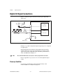
1
DAQ
VXI-AO-48XDC User Manual
DC Setpoint Module for VXIbus
VXI-AO-48XDC User Manual
March 1999 Edition
Part Number 321403B-01
Worldwide Technical Support and Product Information
www.natinst.com
National Instruments Corporate Headquarters
11500 North Mopac Expressway
Austin, Texas 78759-3504
USA Tel: 512 794 0100
Worldwide Offices
Australia 03 9879 5166, Austria 0662 45 79 90 0, Belgium 02 757 00 20, Brazil 011 284 5011,
Canada (Ontario) 905 785 0085, Canada (Québec) 514 694 8521, China 0755 3904939, Denmark 45 76 26 00,
Finland 09 725 725 11, France 01 48 14 24 24, Germany 089 741 31 30, Hong Kong 2645 3186,
India 91805275406, Israel 03 6120092, Italy 02 413091, Japan 03 5472 2970, Korea 02 596 7456,
Mexico (D.F.) 5 280 7625, Mexico (Monterrey) 8 357 7695, Netherlands 0348 433466, Norway 32 27 73 00,
Singapore 2265886, Spain (Madrid) 91 640 0085, Spain (Barcelona) 93 582 0251, Sweden 08 587 895 00,
Switzerland 056 200 51 51, Taiwan 02 2377 1200, United Kingdom 01635 523545
For further support information, see the Technical Support Resources appendix. To comment on the
documentation, send e-mail to [email protected].
© Copyright 1997, 1999 National Instruments Corporation. All rights reserved.
Important Information
Warranty
The VXI-AO-48XDC is warranted against defects in materials and workmanship for a period of one year from the date
of shipment, as evidenced by receipts or other documentation. National Instruments will, at its option, repair or replace
equipment that proves to be defective during the warranty period. This warranty includes parts and labor.
The media on which you receive National Instruments software are warranted not to fail to execute programming
instructions, due to defects in materials and workmanship, for a period of 90 days from date of shipment, as evidenced
by receipts or other documentation. National Instruments will, at its option, repair or replace software media that do not
execute programming instructions if National Instruments receives notice of such defects during the warranty period.
National Instruments does not warrant that the operation of the software shall be uninterrupted or error free.
A Return Material Authorization (RMA) number must be obtained from the factory and clearly marked on the outside
of the package before any equipment will be accepted for warranty work. National Instruments will pay the shipping costs
of returning to the owner parts which are covered by warranty.
National Instruments believes that the information in this document is accurate. The document has been carefully
reviewed for technical accuracy. In the event that technical or typographical errors exist, National Instruments reserves
the right to make changes to subsequent editions of this document without prior notice to holders of this edition. The
reader should consult National Instruments if errors are suspected. In no event shall National Instruments be liable for
any damages arising out of or related to this document or the information contained in it.
EXCEPT AS SPECIFIED HEREIN, NATIONAL INSTRUMENTS MAKES NO WARRANTIES, EXPRESS OR IMPLIED, AND SPECIFICALLY DISCLAIMS
ANY WARRANTY OF MERCHANTABILITY OR FITNESS FOR A PARTICULAR PURPOSE. CUSTOMER’S RIGHT TO RECOVER DAMAGES CAUSED
BY FAULT OR NEGLIGENCE ON THE PART OF NATIONAL INSTRUMENTS SHALL BE LIMITED TO THE AMOUNT THERETOFORE PAID BY THE
CUSTOMER. NATIONAL INSTRUMENTS WILL NOT BE LIABLE FOR DAMAGES RESULTING FROM LOSS OF DATA, PROFITS, USE OF PRODUCTS,
OR INCIDENTAL OR CONSEQUENTIAL DAMAGES, EVEN IF ADVISED OF THE POSSIBILITY THEREOF. This limitation of the liability of
National Instruments will apply regardless of the form of action, whether in contract or tort, including negligence.
Any action against National Instruments must be brought within one year after the cause of action accrues. National
Instruments shall not be liable for any delay in performance due to causes beyond its reasonable control. The warranty
provided herein does not cover damages, defects, malfunctions, or service failures caused by owner’s failure to follow
the National Instruments installation, operation, or maintenance instructions; owner’s modification of the product;
owner’s abuse, misuse, or negligent acts; and power failure or surges, fire, flood, accident, actions of third parties,
or other events outside reasonable control.
Copyright
Under the copyright laws, this publication may not be reproduced or transmitted in any form, electronic or mechanical,
including photocopying, recording, storing in an information retrieval system, or translating, in whole or in part, without
the prior written consent of National Instruments Corporation.
Trademarks
ComponentWorks™, CVI™, LabVIEW™, Measure™, natinst.com™, NI-DAQ™, NI-VISA™, RTSI™, SCXI™, and
VirtualBench™ are trademarks of National Instruments Corporation.
Product and company names mentioned herein are trademarks or trade names of their respective companies.
WARNING REGARDING MEDICAL AND CLINICAL USE OF NATIONAL INSTRUMENTS PRODUCTS
National Instruments products are not designed with components and testing for a level of reliability suitable for use in
or in connection with surgical implants or as critical components in any life support systems whose failure to perform
can reasonably be expected to cause significant injury to a human. Applications of National Instruments products
involving medical or clinical treatment can create a potential for death or bodily injury caused by product failure, or by
errors on the part of the user or application designer. Because each end-user system is customized and differs from
National Instruments testing platforms and because a user or application designer may use National Instruments products
in combination with other products in a manner not evaluated or contemplated by National Instruments, the user or
application designer is ultimately responsible for verifying and validating the suitability of National Instruments products
whenever National Instruments products are incorporated in a system or application, including, without limitation,
the appropriate design, process and safety level of such system or application.
Contents
About This Manual
How To Use the Manual Set..........................................................................................ix
Conventions Used in This Manual.................................................................................ix
Chapter 1
Introduction
About the VXI-AO-48XDC...........................................................................................1-1
What You Need to Get Started ......................................................................................1-1
Software Programming Choices ....................................................................................1-2
National Instruments Application Software ....................................................1-2
NI-DAQ Driver Software ................................................................................1-3
VXIplug&play Instrument Driver ...................................................................1-3
Optional Equipment .......................................................................................................1-4
Custom Cabling ...............................................................................................1-4
Unpacking ......................................................................................................................1-5
Chapter 2
Configuration and Installation
Module Configuration....................................................................................................2-1
VXIbus Logical Address .................................................................................2-3
Hardware Installation.....................................................................................................2-4
Software Installation ......................................................................................................2-5
Chapter 3
Signal Connections
I/O Connector Pin Assignments ....................................................................................3-1
Signal Connection Descriptions ......................................................................3-4
Analog Output Signal Connections ...............................................................................3-5
Voltage Output ................................................................................................3-6
Power-up Condition ..........................................................................3-6
Current Output.................................................................................................3-6
Power-up Condition ..........................................................................3-6
Digital I/O Signal Connections......................................................................................3-8
Power-up Condition.........................................................................................3-8
Power Connections ........................................................................................................3-9
© National Instruments Corporation
v
VXI-AO-48XDC User Manual
Contents
Chapter 4
Hardware Overview
Data Transceivers .......................................................................................................... 4-1
VXIbus Interface Circuitry............................................................................................ 4-2
I/O Connector ................................................................................................................ 4-2
nvRAM/DAC Control..................................................................................... 4-2
Digital I/O Control .......................................................................................... 4-2
Serial Number EPROM................................................................................................. 4-3
Temperature Sensor....................................................................................................... 4-3
Chapter 5
Calibration
Self-Calibration ............................................................................................................. 5-1
External Calibration....................................................................................................... 5-1
Voltage Output Calibration ........................................................................................... 5-2
Offset Adjustment ........................................................................................... 5-2
Gain Adjustment ............................................................................................. 5-2
Current Output Calibration............................................................................................ 5-3
Offset Adjustment ........................................................................................... 5-3
Gain Adjustment ............................................................................................. 5-3
Calibration Programming Considerations ..................................................................... 5-4
Appendix A
Specifications
Appendix B
Common Questions
Appendix C
Technical Support Resources
Glossary
Index
VXI-AO-48XDC User Manual
vi
© National Instruments Corporation
Contents
Figures
Figure 1-1.
The Relationship between the Programming Environment,
Your Instrument Driver, and Your VXI-DAQ Hardware .......................1-4
Figure 2-1.
Figure 2-2.
VXI-AO-48XDC Parts Locator Diagram................................................2-2
Logical Address Selection.......................................................................2-4
Figure 3-1.
Figure 3-2.
Figure 3-3.
Figure 3-4.
Figure 3-5.
CH <0..23> Connector Pin Assignments ................................................3-2
CH <24..47> Connector Pin Assignments ..............................................3-3
VCH Connection as a Voltage Output ....................................................3-5
ICH Connection as a Current Output ......................................................3-7
Digital I/O Connections...........................................................................3-8
Figure 4-1.
VXI-AO-48XDC Block Diagram ...........................................................4-1
Tables
Table 3-1.
Table 3-2.
CH<0..23> Connector Descriptions ........................................................3-4
CH<24..47> Connector Descriptions .....................................................3-4
Table 5-1.
Calibration Channel Numbers ...............................................................5-2
© National Instruments Corporation
vii
VXI-AO-48XDC User Manual
About This Manual
This manual describes the mechanical and electrical aspects of the
VXI-AO-48XDC and contains information concerning its configuration,
installation, and operation. The VXI-AO-48XDC is designed for precise
DC setpoint applications and provides general purpose digital I/O.
How To Use the Manual Set
The VXI-AO-48XDC User Manual is one piece of the documentation set
for your VXI data acquisition (VXI-DAQ) system. You could have any of
several types of documentation, depending on the hardware and software in
your system. Use the different types of documentation you have as follows:
•
Your VXI-DAQ hardware documentation—These documents have
detailed information about the VXI-DAQ hardware that plugs into or
is connected to your computer. Use these documents for hardware
installation and configuration instructions, specification information
about your VXI-DAQ hardware, and application hints.
•
Software documentation—You may have both application software
and driver software documentation. National Instruments application
software includes ComponentWorks, LabVIEW, LabWindows/CVI,
Measure, and VirtualBench. National Instruments driver software
includes NI-DAQ and VXIplug&play instrument drivers. After you
set up your hardware system, use either your application or driver
software documentation to help you write your application. If you have
a large, complicated system, it is worthwhile to look through the
software documentation before you configure your hardware.
•
Accessory installation guides or manuals—If you are using accessory
products, read the terminal block and cable assembly installation
guides or accessory board user manuals. They explain how to
physically connect the relevant pieces of the system. Consult these
guides when you are making your connections.
© National Instruments Corporation
ix
VXI-AO-48XDC User Manual
About This Manual
Conventions Used in This Manual
The following conventions are used in this manual:
<>
Angle brackets containing numbers separated by an ellipsis represent a
range of values associated with a bit or signal name—for example,
Port0_Line<7..0>.
This icon to the left of bold italicized text denotes a note, which alerts you
to important information.
This icon to the left of bold italicized text denotes a warning, which advises
you of precautions to take to avoid being electrically shocked.
bold
Bold text denotes the names of menus, menu items, or dialog box buttons
or options.
bold italic
Bold italic text denotes a note, caution, or warning.
italic
Italic text denotes emphasis, a cross reference, or an introduction to a key
concept.
monospace
Text in this font denotes text or characters that are to be literally input from
the keyboard, sections of code, programming examples, and syntax
examples. This font is also used for the proper names of disk drives, paths,
directories, programs, subprograms, subroutines, device names, functions,
variables, file names and extensions, and for statements and comments
taken from program code.
NI-DAQ
NI-DAQ refers to the NI-DAQ driver software.
VXI-AO-48XDC User Manual
x
© National Instruments Corporation
1
Introduction
This chapter describes the VXI-AO-48XDC, lists what you need to get
started, describes software programming choices, optional equipment,
and custom cables, and explains how to unpack the VXI-AO-48XDC.
About the VXI-AO-48XDC
Thank you for purchasing the National Instruments VXI-AO-48XDC. The
VXI-AO-48XDC is a precise DC setpoint module for the VXIbus. The
module has 48 voltage output channels and 48 current output channels.
In addition, the module has 32 digital I/O lines.
You can use the VXI-AO-48XDC in a wide variety of DC setpoint and
digital applications. With the VXI-AO-48XDC, your VXIbus system can
serve as a digital I/O system controller for laboratory testing, production
testing, and industrial process monitoring and control. Use your
VXI-AO-48XDC module to:
•
Generate experimental stimuli
•
Generate analog functions
•
Connect to a variety of signal types, including:
–
Electromechanical relays
–
LEDs
–
Optically isolated, solid-state relays and I/O module mounting
racks
Detailed specifications for the VXI-AO-48XDC are in Appendix A,
Specifications.
What You Need to Get Started
To set up and use your VXI-AO-48XDC, you will need the following:
❑ VXI-AO-48XDC module
❑ VXI-AO-48XDC User Manual
© National Instruments Corporation
1-1
VXI-AO-48XDC User Manual
Chapter 1
Introduction
❑ One of the following software packages and documentation:
ComponentWorks
LabVIEW for Windows
LabWindows/CVI for Windows
Measure
NI-VISA
NI-DAQ for PC compatibles
VirtualBench
VXIplug&play instrument driver
❑ Your VXIbus system
Software Programming Choices
There are several options to choose from when programming your
National Instruments VXI-DAQ hardware. You can use LabVIEW,
LabWindows/CVI, ComponentWorks, VirtualBench, or other application
development environments with either NI-DAQ or the VXIplug&play
instrument driver. Both NI-DAQ and the VXIplug&play instrument driver
access the VXI-DAQ hardware through the VISA driver software.
National Instruments Application Software
ComponentWorks contains tools for data acquisition and instrument
control built on NI-DAQ driver software. ComponentWorks provides a
higher-level programming interface for building virtual instruments
through standard OLE controls and DLLs. With ComponentWorks, you
can use all of the configuration tools, resource management utilities, and
interactive control utilities included with NI-DAQ.
LabVIEW features interactive graphics, a state-of-the-art user interface,
and a powerful graphical programming language. The LabVIEW Data
Acquisition VI Library, a series of VIs for using LabVIEW with
National Instruments DAQ hardware, is included with LabVIEW.
The LabVIEW Data Acquisition VI Library is functionally equivalent
to the NI-DAQ software.
LabWindows/CVI features interactive graphics, a state-of-the-art user
interface, and uses the ANSI-standard C programming language. The
LabWindows/CVI Data Acquisition Library, a series of functions for using
LabWindows/CVI with National Instruments DAQ hardware, is included
VXI-AO-48XDC User Manual
1-2
© National Instruments Corporation
Chapter 1
Introduction
with the NI-DAQ software kit. The LabWindows/CVI Data Acquisition
Library is functionally equivalent to the NI-DAQ software.
VirtualBench features VIs that combine DAQ products, software, and
your computer to create a standalone instrument with the added benefit
of the processing, display, and storage capabilities of your computer.
VirtualBench instruments load and save waveform data to disk in the
same forms that can be used in popular spreadsheet programs and word
processors.
Using ComponentWorks, LabVIEW, LabWindows/CVI, or VirtualBench
software will greatly reduce the development time for your data acquisition
and control application.
NI-DAQ Driver Software
The NI-DAQ driver software is included at no charge with all National
Instruments DAQ hardware. NI-DAQ is not packaged with accessory
products. NI-DAQ has an extensive library of functions that you can call
from your application programming environment. These functions include
routines for analog input (A/D conversion), buffered data acquisition
(high-speed A/D conversion), analog output (D/A conversion), waveform
generation, digital I/O, counter/timer operations, SCXI, RTSI,
self-calibration, messaging, and acquiring data to extended memory.
NI-DAQ has both high-level DAQ I/O functions for maximum ease of use
and low-level DAQ I/O functions for maximum flexibility and
performance. Examples of high-level functions are streaming data to disk
or acquiring a certain number of data points. An example of a low-level
function is writing directly to registers on the DAQ device. NI-DAQ does
not sacrifice the performance of National Instruments DAQ devices
because it lets multiple devices operate at their peak performance.
NI-DAQ maintains a consistent software interface among its different
versions so that you can change platforms with minimal modifications to
your code.
VXIplug&play Instrument Driver
National Instruments distributes VXIplug&play instrument drivers free of
charge. VXIplug&play instrument drivers are one level above the NI-DAQ
device driver and contain high-level software functions whose architecture
is specified by the VXIplug&play Systems Alliance. The VXIplug&play
standards increase interoperability with other vendors, and ensure that
drivers are designed and presented in a consistent fashion that facilitates
© National Instruments Corporation
1-3
VXI-AO-48XDC User Manual
Chapter 1
Introduction
ease of use. Refer to Figure 1-1 to see the relationship between your
software components.
ComponentWorks,
LabView,
LabWindows/CVI,
or VirtualBench
Other Application
Development Environments
VXIplug&play
Instrument Driver
NI-DAQ Driver Software
VISA
VXI-DAQ Hardware
Figure 1-1. The Relationship between the Programming Environment,
Your Instrument Driver, and Your VXI-DAQ Hardware
Optional Equipment
National Instruments offers a variety of products to use with your
VXI-AO-48XDC module, including cables, connector blocks, and other
accessories, as follows:
•
Cables and cable assemblies, shielded and ribbon
•
Connector blocks, shielded and unshielded screw terminals
For more specific information about these products, refer to your National
Instruments catalogue or call the office nearest you.
Custom Cabling
National Instruments offers cables and accessories for you to
prototype your application or to use if you frequently change module
interconnections.
You can interface the VXI-AO-48XDC to a wide range of test instruments,
I/O racks and modules, screw terminal panels, and almost any device with
a parallel interface. The VXI-AO-48XDC digital I/O connector is a
VXI-AO-48XDC User Manual
1-4
© National Instruments Corporation
Chapter 1
Introduction
standard, 96-pin DIN header connector. Refer to your National Instruments
catalogue for specific information.
Unpacking
Your VXI-AO-48XDC module is shipped in an antistatic package to
prevent electrostatic damage to the module. Electrostatic discharge can
damage several components on the module. To avoid such damage in
handling the module, take the following precautions:
•
Ground yourself via a grounding strap or by holding a grounded object.
•
Touch the antistatic package to a metal part of your VXIbus chassis
before removing the module from the package.
•
Remove the module from the package and inspect the module for loose
components or any other sign of damage. Notify National Instruments
if the module appears damaged in any way. Do not install a damaged
module into your VXIbus backplane.
•
Never touch the exposed pins of connectors.
© National Instruments Corporation
1-5
VXI-AO-48XDC User Manual
Configuration and Installation
2
This chapter describes how to configure and install your VXI-AO-48XDC
module.
Module Configuration
This section describes how to configure the VXIbus logical address on your
VXI-AO-48XDC.
Figure 2-1 shows the VXI-AO-48XDC as it appears with the component
side facing you. The drawing shows the location of various module
components, including the logical address switch.
© National Instruments Corporation
2-1
VXI-AO-48XDC User Manual
Chapter 2
Configuration and Installation
4
3
2
1
5
6
7
8
1
2
Serial Number
S1
3
4
Logical Address Switch
P1 Connector
5
6
Product Name
Assembly Number
7
8
Status Light
Access Light
Figure 2-1. VXI-AO-48XDC Parts Locator Diagram
VXI-AO-48XDC User Manual
2-2
© National Instruments Corporation
Chapter 2
Configuration and Installation
VXIbus Logical Address
Each module in a VXIbus system is assigned a unique number between
0 and 254. This 8-bit number, called the logical address, defines the base
address for the VXIbus configuration registers located on the module. With
unique logical addresses, each VXIbus module in the system is assigned
64 bytes of configuration space in the upper 16 KB of the A16 address
space.
Logical address 0 is reserved for the Resource Manager in the VXIbus
system. Because the VXI-AO-48XDC cannot act as a Resource Manager,
do not configure the VXI-AO-48XDC with a logical address of 0. The
factory-default logical address for the VXI-AO-48XDC is 5.
Some VXIbus modules have dynamically configurable logical addresses.
These modules have an initial logical address of hex FF or decimal 255,
which indicates that they can be dynamically configured.
The VXI-AO-48XDC supports dynamic configuration of its logical
address. However, adding or removing modules can change the logical
address of the VXI-AO-48XDC. Tracking these changes in your
application software can be troublesome.
In many cases, static configuration of the logical address is easier. For
example, ensure that no other statically configurable VXIbus modules have
a logical address of 5. If they do, change the logical address setting of either
the VXI-AO-48XDC or the other module so that every module in the
system has a different logical address.
To change the VXI-AO-48XDC logical address, modify the setting of the
8-bit DIP switch labeled Logical Address Switch (see Figure 2-1 for the
switch location). The down position of the DIP switch corresponds to a
logic value of 0 and the up position corresponds to a logic value of 1. Verify
that the VXI-AO-48XDC does not have the same logical address as any
other statically configured VXIbus module in your system.
Note
Logical address 0 is not allowed for the VXI-AO-48XDC.
© National Instruments Corporation
2-3
VXI-AO-48XDC User Manual
Chapter 2
Configuration and Installation
Figure 2-2 shows switch settings for logical addresses hex 5 and C0.
Logical Address
Switch
Push up for logic 1
Push down for logic 0
1 2 3 4 5 6 7 8
LSB
P1 Connector
MSB
U51
VXI-AO-48XDC Module
a. Switch Set to Logical Address Hex 5 (Default)
Logical Address
Switch
Push up for logic 1
Push down for logic 0
1 2 3 4 5 6 7 8
LSB
P1 Connector
MSB
U51
VXI-AO-48XDC Module
b. Switch Set to Logical Address Hex C0
Figure 2-2. Logical Address Selection
Hardware Installation
This section contains general installation instructions for the
VXI-AO-48XDC. Consult your VXIbus mainframe user manual or
technical reference manual for specific instructions and warnings.
1.
VXI-AO-48XDC User Manual
Plug in your mainframe before installing the VXI-AO-48XDC.
The power cord grounds the mainframe and protects it from
electrical damage while you are installing the module. Do not
turn on the mainframe.
2-4
© National Instruments Corporation
Chapter 2
Warning
Configuration and Installation
To protect both yourself and the mainframe from electrical hazards, do not turn
on the mainframe until you are finished installing the VXI-AO-48XDC module.
2.
Remove or open any doors or covers blocking access to the mainframe
slots.
3.
If you are installing the VXI-AO-48XDC into a D-size mainframe,
first install an appropriate support for C-size modules.
4.
Insert the VXI-AO-48XDC in the slot you have selected:
a.
Align the top and bottom of the module with the card-edge guides
inside the mainframe.
b.
Slowly push the VXI-AO-48XDC straight into the slot until its
plug connectors rest on the backplane receptacle connectors.
c.
Using evenly distributed pressure, slowly press the
VXI-AO-48XDC straight in until it seats in the expansion slot.
d.
Make sure the front panel of the VXI-AO-48XDC is even with the
front panel of the mainframe.
5.
Tighten the retaining screws on the top and bottom edges of the front
panel.
6.
Replace or close any doors or covers to the mainframe.
Software Installation
If you are using a VXIplug&play instrument driver, follow the instructions
in the Setup Utility on the diskettes that were included with your VXI-DAQ
hardware. This user manual assumes that the VISA software is installed. If
VISA is not installed, you must get the VISA software from the supplier of
your VXIbus controller.
If you are using NI-DAQ, refer to your release notes. Find the installation
section for your operating system and follow the instructions given there.
If you are using ComponentWorks, LabVIEW, LabWindows/CVI, or
VirtualBench, refer to the appropriate release notes to install your
application software. After you have installed your application software,
refer to the NI-DAQ release notes and follow the instructions given there
for your operating system and application software.
© National Instruments Corporation
2-5
VXI-AO-48XDC User Manual
3
Signal Connections
This chapter provides connection instructions for the signals on the
VXI-AO-48XDC I/O connector.
Warning
Connections that exceed any of the maximum ratings of input or output signals
on the VXI-AO-48XDC can damage the VXI-AO-48XDC module and the VXIbus
system. Maximum input ratings for each signal are given in this chapter under
the discussion of that signal. National Instruments is not liable for any damages
resulting from any incorrect signal connections.
I/O Connector Pin Assignments
Figures 3-1 and 3-2 show the pin assignments for the VXI-AO-48XDC I/O
connectors.
© National Instruments Corporation
3-1
VXI-AO-48XDC User Manual
Chapter 3
Signal Connections
A
VCH(0)
VCH(1)
VCH(2)
VCH(3)
VCH(4)
VCH(5)
VCH(6)
VCH(7)
VCH(8)
VCH(9)
VCH(10)
VCH(11)
VCH(12)
VCH(13)
VCH(14)
VCH(15)
VCH(16)
VCH(17)
VCH(18)
VCH(19)
VCH(20)
VCH(21)
VCH(22)
VCH(23)
PORT0_LINE1
PORT0_LINE3
PORT0_LINE5
PORT0_LINE7
PORT1_LINE1
PORT1_LINE3
PORT1_LINE5
PORT1_LINE7
32
31
30
29
28
27
26
25
24
23
22
21
20
19
18
17
16
15
14
13
12
11
10
9
8
7
6
5
4
3
2
1
B
ICH(0)
ICH(1)
ICH(2)
ICH(3)
ICH(4)
ICH(5)
ICH(6)
ICH(7)
ICH(8)
ICH(9)
ICH(10)
ICH(11)
ICH(12)
ICH(13)
ICH(14)
ICH(15)
ICH(16)
ICH(17)
ICH(18)
ICH(19)
ICH(20)
ICH(21)
ICH(22)
ICH(23)
PORT0_LINE0
PORT0_LINE2
PORT0_LINE4
PORT0_LINE6
PORT1_LINE0
PORT1_LINE2
PORT1_LINE4
PORT1_LINE6
32
31
30
29
28
27
26
25
24
23
22
21
20
19
18
17
16
15
14
13
12
11
10
9
8
7
6
5
4
3
2
1
C
AGND
AGND
AGND
AGND
AGND
AGND
AGND
AGND
AGND
AGND
AGND
AGND
AGND
AGND
AGND
AGND
AGND
AGND
AGND
AGND
AGND
AGND
AGND
AGND
DGND
DGND
DGND
DGND
DGND
DGND
DGND
+5 V
32
31
30
29
28
27
26
25
24
23
22
21
20
19
18
17
16
15
14
13
12
11
10
9
8
7
6
5
4
3
2
1
Figure 3-1. CH <0..23> Connector Pin Assignments
VXI-AO-48XDC User Manual
3-2
© National Instruments Corporation
Chapter 3
A
VCH(24)
VCH(25)
VCH(26)
VCH(27)
VCH(28)
VCH(29)
VCH(30)
VCH(31)
VCH(32)
VCH(33)
VCH(34)
VCH(35)
VCH(36)
VCH(37)
VCH(38)
VCH(39)
VCH(40)
VCH(41)
VCH(42)
VCH(43)
VCH(44)
VCH(45)
VCH(46)
VCH(47)
PORT2_LINE1
PORT2_LINE3
PORT2_LINE5
PORT2_LINE7
PORT3_LINE1
PORT3_LINE3
PORT3_LINE5
PORT3_LINE7
32
31
30
29
28
27
26
25
24
23
22
21
20
19
18
17
16
15
14
13
12
11
10
9
8
7
6
5
4
3
2
1
B
ICH(24)
ICH(25)
ICH(26)
ICH(27)
ICH(28)
ICH(29)
ICH(30)
ICH(31)
ICH(32)
ICH(33)
ICH(34)
ICH(35)
ICH(36)
ICH(37)
ICH(38)
ICH(39)
ICH(40)
ICH(41)
ICH(42)
ICH(43)
ICH(44)
ICH(45)
ICH(46)
ICH(47)
PORT2_LINE0
PORT2_LINE2
PORT2_LINE4
PORT2_LINE6
PORT3_LINE0
PORT3_LINE2
PORT3_LINE4
PORT3_LINE6
32
31
30
29
28
27
26
25
24
23
22
21
20
19
18
17
16
15
14
13
12
11
10
9
8
7
6
5
4
3
2
1
Signal Connections
C
AGND
AGND
AGND
AGND
AGND
AGND
AGND
AGND
AGND
AGND
AGND
AGND
AGND
AGND
AGND
AGND
AGND
AGND
AGND
AGND
AGND
AGND
AGND
AGND
DGND
DGND
DGND
DGND
DGND
DGND
DGND
+5 V
32
31
30
29
28
27
26
25
24
23
22
21
20
19
18
17
16
15
14
13
12
11
10
9
8
7
6
5
4
3
2
1
Figure 3-2. CH <24..47> Connector Pin Assignments
© National Instruments Corporation
3-3
VXI-AO-48XDC User Manual
Chapter 3
Signal Connections
Signal Connection Descriptions
Tables 3-1 and 3-2 contain descriptions of the signal connections.
Table 3-1. CH<0..23> Connector Descriptions
Pin
Signal Name
Description
A5, B5, A6, B6, A7, B7, A8,
B8
Port0_Line<7..0>
Input/Output Lines for Port 0—Line 7 is
the MSB and Line 0 is the LSB.
A1, B1, A2, B2, A3, B3, A4,
B4
Port1_Line<7..0>
Input/Output Lines for Port 1—Line 7 is
the MSB and Line 0 is the LSB.
B<32..9>
ICH <0..23>
Current output channels.
A<32..9>
VCH <0..23>
Voltage output channels.
C1
+5 V
+5 V—This pin is connected to the VXIbus
system +5 VDC supply through a
self-resetting circuit breaker.
C<32..9>
AGND
Analog Ground—These pins are connected
to the VXI-AO-48XDC analog ground
plane. All VXI-AO-48XDC ground planes
connect to the VXIbus system ground signal.
C<8..2>
DGND
Digital Ground—These pins are connected
to the VXIbus system ground signal. All
VXI-AO-48XDC ground planes connect to
the VXIbus system ground signal.
Table 3-2. CH<24..47> Connector Descriptions
Pin
Signal Name
Description
A5, B5, A6, B6, A7, B7, A8,
B8
Port2_Line<7..0>
Input/Output Lines for Port 2—Line 7 is
the MSB and Line 0 is the LSB.
A1, B1, A2, B2, A3, B3, A4,
B4
Port3_Line<7..0>
Input/Output Lines for Port 3—Line 7 is
the MSB and Line 0 is the LSB
B<32..9>
ICH<24..47>
Current output channels.
A<32..9>
VCH <24..47>
Voltage output channels.
C1
VXI-AO-48XDC User Manual
+5 V
+5 V—This pin is connected to the VXIbus
system +5 VDC supply through a
self-resetting circuit breaker.
3-4
© National Instruments Corporation
Chapter 3
Signal Connections
Table 3-2. CH<24..47> Connector Descriptions (Continued)
Pin
Signal Name
Description
C<32..9>
AGND
Analog Ground—These pins are connected
to the VXI-AO-48XDC analog ground
plane. All VXI-AO-48XDC ground planes
connect to the VXIbus system ground signal.
C<8..2>
DGND
Digital Ground—These pins are connected
to the VXIbus system ground signal. All
VXI-AO-48XDC ground planes connect to
the VXIbus system ground signal.
Refer to Appendix A, Specifications, for detailed information.
Analog Output Signal Connections
Both voltage and current outputs are available on the VXI-AO-48XDC.
This section describes how to make connections for each type of output.
Figure 3-3 shows how to connect the voltage channel (VCH) outputs.
VCH
±10.1 V
Load
AGND
A
Floating Load
Figure 3-3. VCH Connection as a Voltage Output
© National Instruments Corporation
3-5
VXI-AO-48XDC User Manual
Chapter 3
Signal Connections
Voltage Output
You can connect a floating load to your VXI-AO-48XDC module at the
voltage output channel.
Warning
Because the VXI-AO-48XDC module is not electrically isolated from high
voltages, a load with high common mode voltages can damage the
VXI-AO-48XDC module. National Instruments is not liable for any damages
resulting from any such signal connections.
Your VXI-AO-48XDC module has a bipolar voltage range of –10.1 to
+10.1 V. Maximum load current is ±10 mA for 16-bit linearity.
Power-up Condition
•
Output voltage at user-defined value to full accuracy within 1 s of
power-up board reset
Current Output
You can connect a floating or grounded load to your VXI-AO-48XDC
module at the current output channel. You do not need an external floating
power supply to complete the controlled current loop. You can control the
current loop from 0.1 to 20.2 mA. The compliance for the current loop is
0 V to 10 VDC.
Warning
Because the VXI-AO-48XDC module is not electronically isolated from
high voltages, a load with high common mode voltages may damage the
VXI-AO-48XDC module. National Instruments is not liable for any
damages resulting from any such signal connections.
Power-up Condition
VXI-AO-48XDC User Manual
•
Output current: within ±1.1 mA maximum of user-defined current
within 0.5 s of power-up board reset
•
Output current at user-defined value to full accuracy within 7 s of
power-up board reset
3-6
© National Instruments Corporation
Chapter 3
Signal Connections
Figure 3-4 shows how to connect a current channel (ICH) as a current
output.
ICH
Load
0.1 to 20.2 mA
AGND
VXI-AO-48XDC
Figure 3-4. ICH Connection as a Current Output
© National Instruments Corporation
3-7
VXI-AO-48XDC User Manual
Chapter 3
Signal Connections
Digital I/O Signal Connections
Figure 3-5 illustrates signal connections for three typical digital I/O
applications.
+5 V
LED
Port 0
Line<7..0>
R
Port 1
TTL Signal
+5 V
Line<7..0>
Switch
DGND
I/O Connector
VXI-AO-48XDC
Figure 3-5. Digital I/O Connections
In Figure 3-5, port 0 is configured for digital output and port 1 is configured
for digital input.
Digital input applications include receiving TTL signals and sensing
external device states such as the switch in Figure 3-5. Digital output
applications include sending TTL signals and driving external devices
such as the LED shown in Figure 3-5.
Note
The VXI-AO-48XDC allows line-by-line control of digital I/O connections.
Refer to Appendix A, Specifications, for a list of the digital I/O signal
ratings.
Power-up Condition
At power up, ports 0 through 3 of the digital I/O circuitry on the
VXI-AO-48XDC are configured as input ports.
VXI-AO-48XDC User Manual
3-8
© National Instruments Corporation
Chapter 3
Signal Connections
Power Connections
Pin C1 of both I/O connectors is connected to the +5 V supply from the
VXIbus power supply. These pins are referenced to GND and can supply
power to external circuitry. The +5 V supply has a total of 2 A available.
However, you must limit the current through each connector pin to 1.0 A.
The +5 V power supply has a self-resetting protection circuit breaker in
series. If the circuit breaker protection is activated, simply remove the
circuit causing the heavy current load and the circuit breaker will reset
itself. For more information on these output pins, see the Digital I/O and
Power Requirement sections in Appendix A, Specifications.
Power rating
Warning
1.0 A per pin at +5 V ±10%,
+4.55 to +5.25 VDC at 1 A per pin
Under no circumstances should you connect these +5 V power pins directly to
ground or to any other voltage source on the VXI-AO-48XDC or any other device.
Doing so can damage the VXI-AO-48XDC and your VXIbus system. National
Instruments is not liable for damage resulting from such a connection.
© National Instruments Corporation
3-9
VXI-AO-48XDC User Manual
4
Hardware Overview
This chapter contains a functional overview of the VXI-AO-48XDC and
explains the operation of each functional unit making up the module.
The block diagram in Figure 4-1 illustrates the key functional components
of the VXI-AO-48XDC module.
Control/Dtack
VXI Data
VXIbus
Control
Lines
nvRAM/
DAC
Control
DAC
Out
18-bit
DAC
RAM Data
RAM
Addr/Ctrl
Main
Voltage
Circuit
48
Voltage
Output
Circuit X48
Main
Current
Circuit
48
Current
Output
Circuit X48
I/O Connector
VXI
Interface
Logic
VXI Address
nvSRAM
DIO Ports <3..0>
Digital
I/O
+5 V
2.0 A
Self-resetting Circuit Breaker
Figure 4-1. VXI-AO-48XDC Block Diagram
The VXIbus I/O channel consists of an address bus, a data bus, interrupt
lines, and several control and support signals.
Data Transceivers
The data transceivers control the transmission of data to and from
the VXIbus.
© National Instruments Corporation
4-1
VXI-AO-48XDC User Manual
Chapter 4
Hardware Overview
VXIbus Interface Circuitry
An onboard switch setting determines the VXI-AO-48XDC logical
address. The address decoder, which is part of the interface circuitry,
monitors the VXIbus address. If the VXIbus address matches the module’s
selected I/O logical address, the module is enabled and the corresponding
register on the VXI-AO-48XDC is accessed.
In addition, the VXIbus interface circuitry monitors and transmits the
VXIbus interface circuitry signals.
I/O Connector
All I/O is transmitted through two standard, 96-pin header connectors.
See Chapter 2, Configuration and Installation, and Chapter 3, Signal
Connections, for additional information.
nvRAM/DAC Control
The VXI-AO-48XDC has one 18-bit DAC that is time-division
multiplexed to create the 48 voltage and 48 current output channels. Each
voltage and current channel has a track and hold circuit to maintain the
channel value between DAC updates.
Data is stored in an nvRAM (nonvolatile RAM). The nvRAM/DAC control
reads the DAC channel data stored in the nvRAM and updates the DAC
periodically. The nvRAM/DAC control also controls the analog
demultiplexing circuits to route the DAC output to the correct analog output
channel.
You can save nvRAM data, thus allowing power-on values on all analog
channels.
Digital I/O Control
The VXI-AO-48XDC has 32 digital I/O lines configured as four 8-bit
ports. You can configure each line independently as an input or output. The
DIO lines have 12 mA of sink capability and 8 mA of source capability. All
digital lines are TTL compatible. At power up all digital lines are
configured as inputs.
VXI-AO-48XDC User Manual
4-2
© National Instruments Corporation
Chapter 4
Hardware Overview
Serial Number EPROM
The serial number EPROM is a nonvolatile memory used to hold the
module serial number as well as some other identification information
used by the driver software.
Temperature Sensor
The onboard temperature sensor measures the air temperature flowing over
the module. This sensor is positioned near the onboard precision voltage
reference, which can be affected by extreme temperatures. This sensor has
a serial digital interface.
© National Instruments Corporation
4-3
VXI-AO-48XDC User Manual
5
Calibration
This chapter discusses the calibration procedures for your
VXI-AO-48XDC module. Calibration is the process of minimizing
measurement and output voltage errors by making small circuit
adjustments. On the VXI-AO-48XDC, you write values to four
calibration channels to make these adjustments.
Self-Calibration
The VXI-AO-48XDC performs continuous self-calibration. In addition to
the 48 accessible voltage channels and 48 accessible current channels, there
are two voltage channels and two current channels that get scanned and
refreshed along with the others. These four channels are the voltage offset
channel, the voltage gain channel, the current offset channel, and the
current gain channel. The outputs of these four channels are compared to
onboard references, and the 18-bit DAC’s offset and gain are adjusted to
minimize the errors of the four outputs. Since the VXI-AO-48XDC has
excellent channel-to-channel matching of offset and gain errors,
minimizing the errors of the four calibration channels also minimizes the
errors for all the voltage and current outputs.
External Calibration
Because of the nature of the VXI-AO-48XDC calibration circuitry, the
only calibration adjustment you must make is to adjust the values of the
four calibration channels to account for time- or temperature-related drift
of the onboard references. These four values are loaded into nonvolatile
RAM.
Note
The VXI-AO-48XDC is calibrated at the factory to conform to the published
specifications. No recalibration is necessary for at least one year, unless you are
operating the module in extreme temperatures.
To perform calibration, you need a voltage and current measuring device
that is much more accurate than your VXI-AO-48XDC. A DMM with an
accuracy of a few ppm will generally suffice, but be sure to check its
specifications. Also be sure that no other devices are connected to the
© National Instruments Corporation
5-1
VXI-AO-48XDC User Manual
Chapter 5
Calibration
VXI-AO-48XDC when you calibrate it. This will ensure that no ground
loops can corrupt the calibration.
Your VXI-AO-48XDC has a switch to prevent you from accidentally
writing to the calibration channels. Before you can calibrate your module,
you must move the switch (S1) to enable calibration, as labeled on the top
cover. Refer to Figure 2-1, VXI-AO-48XDC Parts Locator Diagram, for the
switch location.
Table 5-1 lists the channel numbers of the calibration channels.
Table 5-1. Calibration Channel Numbers
Calibration Channel
Channel Number
Voltage offset
Voltage channel 48
Voltage gain
Voltage channel 49
Current offset
Current channel 48
Current gain
Current channel 49
Voltage Output Calibration
There are two adjustments to make for the voltage outputs: offset and gain.
You should perform offset adjustment first. It is a good idea to calibrate
twice, because a large change in the voltage gain channel value could
impact the accuracy of the offset calibration.
Offset Adjustment
To calibrate the offset, set one of the voltage output channels to 0 V and
measure it with a precise voltmeter. Then change the voltage offset channel
value until the output is zero. The voltage you write to the voltage offset
channel will be close to zero, and increasing it will lower the voltage you
measure.
Gain Adjustment
To calibrate the gain, set the voltage output channel to a voltage near
full-scale, such as +10 V. Then change the voltage gain channel value until
the output that you measure is as close as possible to the voltage that you
wrote to the output channel. The voltage you write to the voltage gain
channel will be close to +10 V, and increasing it will lower the magnitude
of the voltage you measure.
VXI-AO-48XDC User Manual
5-2
© National Instruments Corporation
Chapter 5
Calibration
You can also calibrate using several output channels instead of just one
by averaging channels together. Do this by writing the values to all the
channels you wish to average and using a resistive averaging circuit to
average the outputs. This will reduce the sensitivity of the calibration
process to interchannel mismatch.
When you are done, save the calibration channel values to nonvolatile
RAM.
Current Output Calibration
There are two adjustments to make for the current outputs: offset and gain.
You should perform offset adjustment first. It is a good idea to calibrate
twice, because a large change in the current gain channel value could
impact the accuracy of the offset calibration.
Offset Adjustment
To calibrate the offset, set one of the current output channels to 100 µA and
measure it with a precise ammeter. Then change the current offset channel
value until the output is as close as possible to 100 µA. The current you
write to the current offset channel will be close to 10 µA, and increasing it
will lower the current you measure.
Gain Adjustment
To calibrate the gain, set the current output channel to a current near
full-scale, such as 20 mA. Then change the current gain channel value until
the output that you measure is as close as possible to the current that you
wrote to the output channel. The current you write to the current gain
channel will be close to 19.608 mA, and increasing it will lower the current
you measure.
You can also calibrate using several output channels instead of just one by
adding channels together. Do this by writing the values to all the channels
you wish to add and summing the outputs by connecting them together.
This will reduce the sensitivity of the calibration process to interchannel
mismatch.
When you are done, save the calibration channel values to
nonvolatile RAM.
© National Instruments Corporation
5-3
VXI-AO-48XDC User Manual
Chapter 5
Calibration
Calibration Programming Considerations
To perform the above-mentioned calibration with the C programming
language, use the NI-DAQ AO_VWrite and AO_Change_Parameter
APIs. Use the AO_Change_Parameter function and the associated
ND_OUTPUT_TYPE parameter to select either the voltage calibration
channels or the current calibration channels. Use the AO_VWrite function
to write the new calibration values to the device. Note that the
AO_Write function does not support the calibration channels because this
function’s interface cannot specify the required precision. Use
the Set_DAQ_Device_Info function and the associated
ND_AO48XDC_SET_POWERUP_STATE parameter to save the new
calibration channel values to nonvolatile RAM.
Refer to the NI-DAQ Function Reference Manual for PC Compatibles for
more information on using these functions to calibrate your
VXI-AO-48XDC module.
To perform the above-mentioned calibration with LabVIEW, use the
AO Update Channel VI and the AO Hardware Config VI. Use the channel
type terminal of the AO Hardware Config VI to select either the voltage
calibration channels or the current calibration channels. Use the AO Update
Channel VI to write the new calibration values to the device. Use the
AO Parameter VI and select the Save Power-on State option to save the
new calibration channel values to nonvolatile RAM.
VXI-AO-48XDC User Manual
5-4
© National Instruments Corporation
A
Specifications
This appendix lists the VXI-AO-48XDC specifications. These
specifications are valid for an ambient temperature of 0 to 55 °C,
unless otherwise stated.
Analog Output
Number of voltage channels .................. 48
Number of current channels ................... 48
Resolution .............................................. 18-bit
Type of DAC.......................................... double-buffered, self-calibrating
Transfer Characteristics
Relative accuracy (INL)......................... ±3 LSB max
DNL ....................................................... ±2 LSB max
Monotonicity.......................................... 17 bits, guaranteed
Voltage Output
Range ..................................................... ±10.1 V
Output coupling...................................... DC
Output impedance .................................. 0.1 Ω max
Current drive .......................................... ±10 mA max
Load capacitance.................................... 10,000 pF max
Protection ............................................... Short circuit to ground
Absolute accuracy .................................. ±1 mV max
Noise ...................................................... 100 µV rms, DC to 1 MHz
© National Instruments Corporation
A-1
VXI-AO-48XDC User Manual
Appendix A
Specifications
Current Output
Range ......................................................0.1 to 20.2 mA
Type ........................................................Source, does not require external
excitation source
Output impedance...................................1 GΩ min
Output compliance..................................0 to 10 V
Absolute accuracy...................................±7 µA max
Noise .......................................................1 µA rms, DC to 1 MHz
Protection................................................Short circuit and open circuit
Dynamic Characteristics
Settling time (including channel latency)
Accuracy
±0.1%
±0.01%
±0.001%
5 ms typ,
12 ms max
10 ms typ,
24 ms max
40 ms typ,
100 ms max
Stability
Offset temperature coefficient
voltage .............................................5 µV/°C
current..............................................10 nA/°C
Gain temperature coefficient
voltage .............................................1 ppm/°C
current..............................................2 ppm/°C
Digital I/O
Number of channels................................32 I/O
Compatibility ..........................................TTL
VXI-AO-48XDC User Manual
A-2
© National Instruments Corporation
Appendix A
Specifications
Digital logic levels
Level
Min
Max
Input low voltage
—
0.8 V
Input high voltage
2.0 V
—
Output low voltage
—
0.4 V, IOL = 12 mA
Output high voltage
2.4 V, IOH = 8 mA
—
Input leakage current
—
10 µA
Bus Interface
Type ....................................................... Slave
Power Requirement
+5 V........................................................ 2 A
+12 V...................................................... 800 mA
–12 V...................................................... 800 mA
+24 V...................................................... 100 mA
–24 V...................................................... 100 mA
Note
These power usage figures do not include the power used by external devices that
are connected to the fused supply present on the I/O connector. They assume that
all voltage and current outputs are fully loaded.
Physical
Dimensions............................................. VXI C-size single slot
I/O connector.......................................... 96-pin (DIN x 2)
© National Instruments Corporation
A-3
VXI-AO-48XDC User Manual
Appendix A
Specifications
Environment
Operating
Temperature............................................0 to 55 °C ambient
Relative humidity ...................................5% to 90% noncondensing
Storage
Temperature............................................–20 to 70 °C ambient
Relative humidity ...................................5% to 90% noncondensing
VXI-AO-48XDC User Manual
A-4
© National Instruments Corporation
B
Common Questions
This appendix contains commonly asked questions and their answers
relating to usage and special features of your VXI-AO-48XDC module.
General Information
What if I short-circuit the power supply on the VXI-AO-48XDC
connector?
Pin C1 of the I/O connectors is connected to the +5 V supply from the
VXIbus power supply. These pins are referenced to GND and can be used
to power external circuitry. The +5 V supply has a total of 2 A available.
However, the current through each connector pin must be limited to 1.0 A.
Each power supply has a self-resetting protection circuit breaker in series.
If the circuit breaker protection is activated, simply remove the circuit
causing the heavy current load and the circuit breaker will reset itself. For
more information on these output pins, see the Digital I/O and Power
Requirement sections in Appendix A, Specifications.
Installation and Configuration
What jumpers/switches should I be aware of when configuring my
VXI-AO-48XDC module?
The only switch you must configure is the logical address switch. Refer to
the VXIbus Logical Address section of Chapter 2, Configuration and
Installation, for this information.
Which National Instruments document should I read first to get
started using DAQ software?
The release notes document for your application or driver software is
always the best starting place.
What version of NI-DAQ must I have to program my VXI-AO-48XDC
module?
You must have NI-DAQ for PC compatibles version 5.0 or higher for your
VXI-AO-48XDC module.
© National Instruments Corporation
B-1
VXI-AO-48XDC User Manual
Appendix B
Common Questions
What is the best way to test my module without having to program it?
The NI-DAQ Test Panels provide a quick and easy way for you to test the
functionality of your module. To run Test Panels from Measurement &
Automation Explorer, go to the Devices and Interfaces view and
right-click on the icon for the module to be tested. Select Properties. In the
System panel, click the Run Test Panels button.
Timing and Digital I/O
What are the power-on states of the DIO lines on the I/O connector?
At system power-on and reset, all ports are configured as inputs. Refer to
the Digital I/O Control section in Chapter 4, Hardware Overview, for more
information.
Analog Output
What are the power-on states of the voltage and current outputs?
At system power-on and reset, all analog outputs are at the values you last
saved.
How fast does the VXI-AO-48XDC module scan channels?
The VXI-AO-48XDC has one 18-bit DAC that is time-division multiplexed
to create the 48 voltage and 48 current output channels. Thus a channel can
change value a maximum of 5 ms after it has been updated by software.
How are the voltage and current outputs related?
They are completely independent of each other.
VXI-AO-48XDC User Manual
B-2
© National Instruments Corporation
Technical Support Resources
C
This appendix describes the comprehensive resources available to you in
the Technical Support section of the National Instruments Web site and
provides technical support telephone numbers for you to use if you have
trouble connecting to our Web site or if you do not have internet access.
NI Web Support
To provide you with immediate answers and solutions 24 hours a day,
365 days a year, National Instruments maintains extensive online technical
support resources. They are available to you at no cost, are updated daily,
and can be found in the Technical Support section of our Web site at
www.natinst.com/support.
Online Problem-Solving and Diagnostic Resources
•
KnowledgeBase—A searchable database containing thousands of
frequently asked questions (FAQs) and their corresponding answers or
solutions, including special sections devoted to our newest products.
The database is updated daily in response to new customer experiences
and feedback.
•
Troubleshooting Wizards—Step-by-step guides lead you through
common problems and answer questions about our entire product line.
Wizards include screen shots that illustrate the steps being described
and provide detailed information ranging from simple getting started
instructions to advanced topics.
•
Product Manuals—A comprehensive, searchable library of the latest
editions of National Instruments hardware and software product
manuals.
•
Hardware Reference Database—A searchable database containing
brief hardware descriptions, mechanical drawings, and helpful images
of jumper settings and connector pinouts.
•
Application Notes—A library with more than 100 short papers
addressing specific topics such as creating and calling DLLs,
developing your own instrument driver software, and porting
applications between platforms and operating systems.
© National Instruments Corporation
C-1
VXI-AO-48XDC User Manual
Appendix C
Technical Support Resources
Software-Related Resources
•
Instrument Driver Network—A library with hundreds of instrument
drivers for control of standalone instruments via GPIB, VXI, or serial
interfaces. You also can submit a request for a particular instrument
driver if it does not already appear in the library.
•
Example Programs Database—A database with numerous,
non-shipping example programs for National Instruments
programming environments. You can use them to complement the
example programs that are already included with National Instruments
products.
•
Software Library—A library with updates and patches to application
software, links to the latest versions of driver software for National
Instruments hardware products, and utility routines.
Worldwide Support
National Instruments has offices located around the globe. Many branch
offices maintain a Web site to provide information on local services. You
can access these Web sites from www.natinst.com/worldwide.
If you have trouble connecting to our Web site, please contact your local
National Instruments office or the source from which you purchased your
National Instruments product(s) to obtain support.
For telephone support in the United States, dial 512 795 8248. For
telephone support outside the United States, contact your local branch
office:
Australia 03 9879 5166, Austria 0662 45 79 90 0, Belgium 02 757 00 20,
Brazil 011 284 5011, Canada (Ontario) 905 785 0085,
Canada (Québec) 514 694 8521, China 0755 3904939,
Denmark 45 76 26 00, Finland 09 725 725 11, France 01 48 14 24 24,
Germany 089 741 31 30, Hong Kong 2645 3186, India 91805275406,
Israel 03 6120092, Italy 02 413091, Japan 03 5472 2970,
Korea 02 596 7456, Mexico (D.F.) 5 280 7625,
Mexico (Monterrey) 8 357 7695, Netherlands 0348 433466,
Norway 32 27 73 00, Singapore 2265886, Spain (Madrid) 91 640 0085,
Spain (Barcelona) 93 582 0251, Sweden 08 587 895 00,
Switzerland 056 200 51 51, Taiwan 02 2377 1200,
United Kingdom 01635 523545
VXI-AO-48XDC User Manual
C-2
www.natinst.com
Glossary
Prefix
Meanings
Value
n-
nano-
10 –9
µ-
micro-
10 – 6
m-
milli-
10 –3
k-
kilo-
10 3
M-
mega-
10 6
G-
giga-
10 9
Symbols
~
approximately
°
degrees
–
negative of, or minus
Ω
ohms
/
per
%
percent
±
plus or minus
+
positive of, or plus
A
A
amperes
A16 space
VXIbus address space equivalent to the VME 64 KB short address space.
In VXI, the upper 16 KB of A16 space is allocated for use by VXI module’s
configuration registers. This 16 KB region is referred to as VXI
configuration space.
© National Instruments Corporation
G-1
VXI-AO-48XDC User Manual
Glossary
A/D
analog-to-digital
address space
A set of 2n memory locations differentiated from other such sets in
VXI/VMEbus systems by six addressing lines known as address modifiers.
n is the number of address lines required to uniquely specify a byte location
in a given space. Valid numbers for n are 16, 24, and 32. In VME/VXI,
because there are six address modifiers, there are 64 possible address
spaces.
address window
A portion of address space that can be accessed from the application
program.
ANSI
American National Standards Institute.
API
application programming interface
B
backplane
An assembly, typically a printed circuit board, with 96-pin connectors and
signal paths that bus the connector pins. VXIbus systems will have two sets
of bused connectors, called the J1 and J2 backplanes, or have three sets of
bused connectors, called the J1, J2, and J3 backplane.
base address
A memory address that serves as the starting address for programmable
registers. All other addresses are located by adding to the base address.
BCD
binary-coded decimal
bit
One binary digit, either 0 or 1.
bus
The group of conductors that interconnect individual circuitry in a
computer. Typically, a bus is the expansion vehicle to which I/O or other
devices are connected.
byte
Eight related bits of data, an eight-bit binary number. Also used to denote
the amount of memory required to store one byte of data.
VXI-AO-48XDC User Manual
G-2
© National Instruments Corporation
Glossary
C
C
Celsius
channel
Pin or wire lead to which you apply or from which you read the analog or
digital signal. Analog signals can be single-ended or differential. For digital
signals, you group channels to form ports. Ports usually consist of either
four or eight digital channels.
Configuration Registers
(1) A set of registers through which the system can identify a module
device type, model, manufacturer, address space, and memory
requirements. In order to support automatic system and memory
configuration, the VXIbus specification requires that all VXIbus devices
have a set of such registers. (2) The A16 registers of a device that are
required for the system configuration process.
D
D/A
digital-to-analog
DAQ
data acquisition—(1) Collecting and measuring electrical signals from
sensors, transducers, and test probes or fixtures and inputting them to a
computer for processing; (2) Collecting and measuring the same kinds of
electrical signals with A/D and/or DIO boards plugged into a computer, and
possibly generating control signals with D/A and/or DIO boards in the
same computer.
default setting
A default parameter value recorded in the driver. In many cases, the default
input of a control is a certain value (often 0) that means use the current
default setting. For example, the default input for a parameter may be do
not change current setting, and the default setting may be no AMUX-64T
boards. If you do change the value of such a parameter, the new value
becomes the new setting. You can set default settings for some parameters
in the configuration utility or by manually using switches located on the
device.
© National Instruments Corporation
G-3
VXI-AO-48XDC User Manual
Glossary
device
(1) A plug-in data acquisition board, card, or pad that can contain multiple
channels and conversion devices. Plug-in boards, PCMCIA cards, and
devices such as the DAQPad-1200, which connects to your computer
parallel port, are all examples of DAQ devices. (2) A component of a
VXIbus system, normally one VXIbus board. However, multiple-slot
devices and multiple-device modules can operate on a VXIbus system as a
single device. Some examples of devices are computers, multimeters,
multiplexers, oscillators, operator interfaces, and counters.
digital input group
A collection of digital input ports. You can associate each group with its
own clock rates, handshaking modes, buffer configurations, and so on. A
port cannot belong to more than one group.
digital output group
A collection of digital output ports. You can associate each group with its
own clock rates, handshaking modes, buffer configurations, and so on. A
port cannot belong to more than one group.
digital trigger
A TTL-level signal having two discrete levels—high and low.
DIN
Deutsche Industrie Norme
DIO
digital input/output
DIP
dual inline package
dithering
The addition of Gaussian noise to an analog input signal.
DLL
Dynamic Link Library—A software module in Microsoft Windows
containing executable code and data that can be called or used by Windows
applications or by other DLLs. Functions and data in a DLL are loaded and
linked at run time when they are referenced by a Windows application or
other DLLs.
DMA
direct memory access
DRAM
Dynamic RAM
drivers/driver software
Software that controls a specific hardware device such as a DAQ board.
dual-access memory
Memory that can be sequentially, but not simultaneously, accessed by more
than one controller or processor. Also known as shared memory.
dual-ported memory
Memory that can be simultaneously accessed by more than one controller
or processor.
VXI-AO-48XDC User Manual
G-4
© National Instruments Corporation
Glossary
dynamic configuration
A method of automatically assigning logical addresses to VXIbus devices
at system startup or other configuration times. Each slot can contain one or
more devices. Different devices within a slot can share address decoding
hardware.
dynamic range
The ratio of the largest signal level a circuit can handle to the smallest
signal level it can handle (usually taken to be the noise level), normally
expressed in dB.
dynamically configured
device
A device that has its logical address assigned by the Resource Manager. A
VXI device initially responds at Logical Address 255 when its MODID line
is asserted. The Resource Manager subsequently assigns it a new logical
address, which the device responds to until powered down.
E
embedded controller
An intelligent CPU (controller) interface plugged directly into the VXI
backplane, giving it direct access to the VXIbus. It must have all of its
required VXI interface capabilities built in.
EPROM
Erasable Programmable Read-Only Memory (ROM) that can be erased
(usually by ultraviolet light exposure) and reprogrammed.
event
Signals or interrupts generated by a device to notify another device of an
asynchronous event. The contents of events are device-dependent.
external controller
In this configuration, a plug-in interface board in a computer is connected
to the VXI mainframe via one or more VXIbus extended controllers. The
computer then exerts overall control over VXIbus system operations.
external trigger
A voltage pulse from an external source that triggers an event such as A/D
conversion.
F
floating signal sources
Signal sources with voltage signals that are not connected to an absolute
reference or system ground. Also called nonreferenced signal sources.
Some common example of floating signal sources are batteries,
transformers, or thermocouples.
ft
feet
© National Instruments Corporation
G-5
VXI-AO-48XDC User Manual
Glossary
function
A set of software instructions executed by a single line of code that may
have input and/or output parameters and returns a value when executed.
G
GND
ground signal or bit
H
hardware
The physical components of a computer system, such as the circuit boards,
plug-in boards, chassis, enclosures, peripherals, cables, and so on.
hardware triggering
A form of triggering where you set the start time of an acquisition and
gather data at a known position in time relative to a trigger signal.
hex
hexadecimal
Hz
hertz—A unit of frequency equal to one cycle per second.
I
IC
integrated circuit
in.
inches
INL
Integral Nonlinearity—A measure in LSB of the worst-case deviation from
the ideal A/D or D/A transfer characteristic of the analog I/O circuitry.
input range
The difference between the maximum and minimum voltages an analog
input channel can measure at a gain of 1. The input range is a scalar value,
not a pair of numbers. By itself the input range does not uniquely determine
the upper and lower voltage limits. An input range of 10 V could mean an
upper limit of +10 V and a lower of 0 V or an upper limit of +5 V and a
lower limit of –5 V. The combination of input range, polarity, and gain
determines the input limits of an analog input channel. For some boards,
jumpers set the input range and polarity, while you can program them for
other boards. Most boards have programmable gains.
instrument driver
A set of high-level software functions that controls a specific VXI or
RS-232 programmable instrument or a specific plug-in DAQ board.
VXI-AO-48XDC User Manual
G-6
© National Instruments Corporation
Glossary
interrupt
A computer signal indicating that the CPU should suspend its current task
to service a designated activity.
interrupt level
The relative priority at which a device can interrupt.
interval scanning
Scanning method where there is a longer interval between scans than there
is between individual channels comprising a scan.
I/O
Input/output—The transfer of data to/from a computer system involving
communications channels, operator interface devices, and/or data
acquisition and control interfaces.
K
KB
kilobytes—1,024 bytes when referring to memory
kS
1,000 samples
L
latched digital I/O
A type of digital acquisition/generation where a device or module accepts
or transfers data after a digital pulse has been received. Also called
handshaked digital I/O.
LED
light-emitting diode
logical address
An 8-bit number that uniquely identifies each VXIbus device in a system.
It defines the A16 register addresses of a device, and indicates Commander
and Servant relationships.
LSB
least significant bit
M
m
meters
mainframe
The chassis of a VXI system that mechanically contains VXI modules
inserted into the backplane, ensuring that connectors fit properly and that
adjacent modules do not contact each other. It also provides cooling airflow,
and ensures that modules do not disengage from the backplane due to
vibration or shock.
© National Instruments Corporation
G-7
VXI-AO-48XDC User Manual
Glossary
MANTIS
A National Instruments custom ASIC.
MB
megabytes of memory
memory device
A memory storage device that has configuration registers.
MITE
A National Instruments custom ASIC. A sophisticated dual-channel DMA
controller that incorporates the Synchronous MXI and VME64 protocols to
achieve high-performance block transfer rates.
module
Typically a board assembly and its associated mechanical parts, front panel,
optional shields, and so on. A module contains everything required to
occupy one or more slots in a mainframe.
MSB
most significant bit
multitasking
A property of an operating system in which several processes can be run
simultaneously.
N
NC
Normally closed, or not connected
NI-DAQ
National Instruments driver software for DAQ hardware
node
Execution elements of a block diagram consisting of functions, structures,
and subVIs
noise
An undesirable electrical signal—Noise comes from external sources such
as the AC power line, motors, generators, transformers, fluorescent lights,
soldering irons, CRT displays, computers, electrical storms, welders, radio
transmitters, and internal sources such as semiconductors, resistors, and
capacitors. Noise corrupts signals you are trying to send or receive.
non-slot 0 device
A device configured for installation in any slot in a VXIbus mainframe
other than Slot 0. Installing such a device into Slot 0 can damage the device,
the VXIbus backplane, or both.
nvRAM
nonvolatile RAM
VXI-AO-48XDC User Manual
G-8
© National Instruments Corporation
Glossary
O
operating system
Base-level software that controls a computer, runs programs, interacts with
users, and communicates with installed hardware or peripheral devices.
optical isolation
The technique of using an optoelectric transmitter and receiver to transfer
data without electrical continuity, to eliminate high-potential differences
and transients.
output limits
The upper and lower voltage or current outputs for an analog output
channel. The output limits determine the polarity and voltage reference
settings for a board.
output settling time
The amount of time required for the analog output voltage to reach its final
value within specified limits.
P
PC
personal computer
port
(1) A communications connection on a computer or a remote controller. (2)
A digital port, consisting of four or eight lines of digital input and/or output.
PPI
programmable peripheral interface
ppm
parts per million
R
RAM
random access memory
resolution
The smallest signal increment that can be detected by a measurement
system. Resolution can be expressed in bits, in proportions, or in percent
of full scale. For example, a system has 12-bit resolution, one part in
4,096 resolution, and 0.0244 percent of full scale.
Resource Manager
A message-based Commander, located at logical address 0, which provides
configuration management services such as address map configuration,
Commander and Servant mappings, and self-test and diagnostics
management
© National Instruments Corporation
G-9
VXI-AO-48XDC User Manual
Glossary
responses
Signals or interrupts generated by a device to notify another device of an
asynchronous event. Responses contain the information in the Response
register of a sender.
RTSI
Real-Time System Integration
S
s
seconds
S
sample
settling time
The amount of time required for a voltage to reach its final value within
specified limits.
signal
Any communication between message-based devices consisting of a write
to a Signal register.
slot
A position where a module can be inserted into a VXIbus backplane.
Each slot provides the 96-pin J connectors to interface with the board
P connectors. A slot can have one, two, or three connectors.
slot 0 device
A VXIbus device that provides basic resources to VXI Slots 1 through 12.
For B and C-size systems, the resources provided are CLK10 and MODID.
For a D-size system, the Slot 0 device also provides CLK100.
S/s
Samples per Second—Used to express the rate at which a DAQ board
samples an analog signal.
statically configured
device
A device whose logical address cannot be set through software; that is, it is
not dynamically configurable.
system
A system consists of one or more mainframes that are connected, all
sharing a common Resource Manager. Each device in a system has a unique
logical address.
system RAM
RAM installed on a personal computer and used by the operating system,
as contrasted with onboard RAM.
VXI-AO-48XDC User Manual
G-10
© National Instruments Corporation
Glossary
T
transfer rate
The rate, measured in bytes/s, at which data is moved from source to
destination after software initialization and set up operations; the maximum
rate at which the hardware can operate.
TTL
Transistor-transistor logic
U
update
The output equivalent of a scan. One or more analog or digital output
samples. Typically, the number of output samples in an update is equal to
the number of channels in the output group. For example, one pulse from
the update clock produces one update which sends one new sample to every
analog output channel in the group.
update rate
The number of output updates per second.
V
V
volts
VDC
volts direct current
VI
Virtual Instrument—(1) A combination of hardware and/or software
elements, typically used with a PC, that has the functionality of a classic
stand-alone instrument. (2) A LabVIEW software module (VI), which
consists of a front panel user interface and a block diagram program.
VISA
A new driver software architecture developed by National Instruments to
unify instrumentation software (GPIB, DAQ, and VXI). It has been
accepted as a standard for VXI by the VXIplug&play Systems Alliance.
VXIbus
VMEbus eXtensions for Instrumentation
VXIplug&play
Systems Alliance
A group of VXI developers dedicated to making VXI devices as easy to use
as possible, primarily by simplifying software development.
© National Instruments Corporation
G-11
VXI-AO-48XDC User Manual
Glossary
W
waveform
Multiple voltage readings taken at a specific sampling rate
wire
Data path between nodes.
word serial
The simplest required communication protocol used by message-based
devices in the VXIbus system. It uses the A16 communication registers to
transfer data with a simple polling handshake method.
VXI-AO-48XDC User Manual
G-12
© National Instruments Corporation
Index
Numbers
programming considerations, 5-4
self calibration, 5-1
voltage output calibration, 5-2 to 5-3
gain adjustment, 5-2 to 5-3
offset adjustment, 5-2
CH<0..23> connector
pin assignments (figure), 3-2
signal descriptions (table), 3-4
CH<24..47> connector
pin assignments (figure), 3-3
signal descriptions (table), 3-4 to 3-5
circuit breaker, self-resetting, 3-8, 4-1
circuitry, VXIbus interface, 4-2
common questions. See questions about
VXI-AO-48XDC.
ComponentWorks application software, 1-2
configuration. See also installation.
common questions, B-1 to B-2
parts locator diagram, 2-2
VXIbus logical address, 2-3 to 2-4
current output, 3-6 to 3-7
calibration
gain adjustment, 5-3
offset adjustment, 5-3
damage due to high common mode voltages
(warning), 3-6
ICH connection as current output
(figure), 3-7
power-up condition, 3-6
specifications, A-1 to A-2
+5 V signal
CH<0..23> connector (table), 3-4
CH<24..47> connector (table), 3-4
A
AGND signal (table), 3-5
analog output connections, 3-5 to 3-7
common questions, B-2
current output, 3-6 to 3-7
damage due to high common mode
voltages (warning), 3-6
ICH connection as current output
(figure), 3-7
power-up condition, 3-6
specifications, A-1
voltage output, 3-6
damage due to high common mode
voltages (warning), 3-6
power-up condition, 3-6
VCH connection as voltage output
(figure), 3-5
B
bus interface specifications, A-3
C
cabling, custom, 1-5
calibration, 5-1 to 5-4
current output calibration, 5-3
gain adjustment, 5-3
offset adjustment, 5-3
external calibration, 5-1 to 5-2
channel numbers (table), 5-2
© National Instruments Corporation
D
data transceivers, 4-2
DGND signal (table), 3-5
digital I/O connections
description, 3-8
I-1
VXI-AO-48XDC User Manual
Index
software installation, 2-6
unpacking VXI-AO-48XDC, 1-5
interface, VXIbus circuitry, 4-2
I/O connector
digital I/O control, 4-3
nvRAM/DAC control, 4-2
pin assignments
CH<0..23> connector (figure), 3-2
CH<24..47> connector (figure), 3-3
overview of digital I/O control, 4-3
power-on states of DIO lines, B-2
power-up condition, 3-8
specifications, A-2 to A-3
typical digital I/O applications (figure),
3-7
documentation
conventions used in manual, x
how to use the manual set, ix
dynamic characteristic specifications, A-2
L
E
LabVIEW software, 1-3
LabWindows/CVI software, 1-3
logical address, VXIbus, 2-3 to 2-4
configuration, 2-3
switch settings, 2-4
environment specifications, A-4
EPROM, serial number, 4-3
equipment, optional, 1-5
external calibration, 5-1 to 5-2
channel numbers (table), 5-2
M
H
manual. See documentation.
module configuration. See configuration.
hardware installation, 2-5
hardware overview
block diagram, 4-1
data transceivers, 4-2
I/O connector
digital I/O control, 4-3
nvRAM/DAC control, 4-2
serial number EPROM, 4-3
temperature sensor, 4-3
VXIbus interface circuitry, 4-2
N
NI-DAQ driver software, 1-3 to 1-4
nvRAM/DAC control, 4-2
O
optional equipment, 1-5
I
P
ICH connection as current output (figure), 3-7
ICH<0..23> signal (table), 3-4
ICH<24..47> signal (table), 3-4
installation. See also configuration.
common questions, B-1 to B-2
hardware installation, 2-5
physical specifications, A-3
pin assignments
CH<0..23> connector (figure), 3-2
CH<24..47> connector (figure), 3-3
Port0_Line<7..0> signal (table), 3-4
Port1_Line<7..0> signal (table), 3-4
Port2_Line<7..0> signal (table), 3-4
VXI-AO-48XDC User Manual
I-2
© National Instruments Corporation
Index
CH<24..47> connector (figure), 3-3
power connections, 3-8
software installation, 2-6
software programming choices, 1-2 to 1-4
National Instruments application
software, 1-2 to 1-3
NI-DAQ driver software, 1-3 to 1-4
VXIplug&play instrument driver, 1-4
specifications
analog output, A-1
bus interface, A-3
current output, A-1 to A-2
digital I/O, A-2 to A-3
dynamic characteristics, A-2
environment, A-4
physical, A-3
power requirements, A-3
stability, A-2
transfer characteristics, A-1
voltage output, A-1
stability specifications, A-2
Port3_Line<7..0> signal (table), 3-4
power connections
connecting directly to ground
(warning), 3-8
description, 3-8
power requirement specifications, A-3
power-up condition
current output, 3-6
digital I/O connections, 3-8
voltage output, 3-6
programming considerations for
calibration, 5-4
Q
questions about VXI-AO-48XDC
analog output, B-2
general information, B-1
installation and configuration, B-1 to B-2
timing and digital I/O, B-2
S
T
self calibration, 5-1
serial number EPROM, 4-3
signal connections
analog output connections, 3-5 to 3-7
current output, 3-6 to 3-7
VCH connection as voltage output
(figure), 3-5
voltage output, 3-6
digital I/O connections, 3-7 to 3-8
power-up condition, 3-8
exceeding maximum ratings
(warning), 3-1
I/O connector pin description
CH<0..23> connector descriptions
(table), 3-2
CH<0..23> connector (figure), 3-2
CH<24..47> connector descriptions
(table), 3-4 to 3-5
© National Instruments Corporation
technical support, C-1 to C-2
telephone support, C-2
temperature sensor, 4-3
theory of operation. See hardware overview.
timing and digital I/O, B-2
transfer characteristic specifications, A-1
U
unpacking VXI-AO-48XDC, 1-5
V
VCH connection as voltage output
(figure), 3-5
VCH<0..23> signal (table), 3-4
VCH<24..47> signal (table), 3-4
I-3
VXI-AO-48XDC User Manual
Index
VirtualBench software, 1-3
voltage output, 3-6
calibration, 5-2 to 5-3
gain adjustment, 5-2 to 5-3
offset adjustment, 5-2
damage due to high common mode
voltages (warning), 3-6
power-up condition, 3-6
specifications, A-1
VCH connection as voltage output
(figure), 3-5
VXI-AO-48XDC
block diagram, 4-1
custom cabling, 1-5
features, 1-1
optional equipment, 1-5
overview, 1-1
requirements for getting started, 1-2
software programming choices, 1-2 to 1-4
National Instruments application
software, 1-2 to 1-3
NI-DAQ driver software, 1-3 to 1-4
VXIplug&play instrument
driver, 1-4
unpacking, 1-5
VXIbus interface circuitry, 4-2
VXIbus logical address, 2-3 to 2-4
configuration, 2-3
switch settings (figure), 2-4
VXIplug&play instrument driver, 1-4
VXI-AO-48XDC User Manual
I-4
© National Instruments Corporation