1
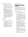
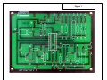
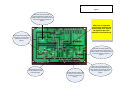
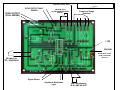
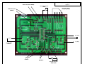
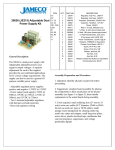
Jameco Part Number 20685
(JE2206)
Function Generator Kit
GENERAL DESCRIPTION
The 20685 (JE2206 Function Generator Kit) is a
single-board assembly incorporating the basic
circuit necessary for a sine, square, and triangle
wave generator, of high stability and accuracy that
may be amplitude and frequency modulated. The
kit is intended to be incorporated into a higher
assembly of the user's own design that adds power
supply, controls, and housing.
•
•
•
•
•
•
•
•
•
Operating from either a +12VDC or +/6VDC @ 15mA power source
Frequency capability: +1 to 100KHz in 4
ranges
Frequency variability: 1:100 within each
range
Frequency accuracy dependent upon
timing capacitors and user's potentiometer
(calibration by user)
Sine / triangle output amplitudes variable,
0 to 6Vp-p for sine and 0V to V+/- for
triangle, with 600Ω source impedance
Maximum sine wave distortion: 1% 10 to
10kHz; and 3% 10 to 100kHz
Linear frequency modulation capability
range dependent on center frequency
Linear amplitude modulation capability,
range 55dB
Other criteria as determined by Exar 2206
function generator IC
Component Part
Reference
Number
Description
Qty.
IC1
34972
1
C1, C2, C7
10882
C3
27001
C4
26956
C5
26884
C6
26833
R1
691219
R2
691340
R3, R7
690865
R4
691091
R5, R6
691032
R8
690734
R9
42981
IC Function Generator
XR2206
Electrolytic Capacitor,
AXIAL, 10uF @ 50V
Mylar capacitor, nonpolarized, 1uF @ 100V
(1K)
Mylar capacitor, nonpolarized, 0.1uF @
100V (104)
Mylar capacitor, nonpolarized, 0.01uF @
100V (0.01)
Mylar capacitor, nonpolarized, 0.001uF @
100V (102)
1/4W Resistor, 30k
(orange-black-orange)
1/4W Resistor, 100k
(brown-black-yellow)
1/4W Resistor, 1k
(brown-black-red)
1/4W Resistor, 9.1k
(white-brown-red)
1/4W Resistor, 5.1k
(green-brown-red)
1/4W Resistor, 300Ω
(orange-black-brown)
Potentiometer, 1M (105)
R10
42964
Potentiometer, 1k (102)
1
R11
35511
134341
Potentiometer, 25k (253)
22AWG black hook up
wire
JE2206-1 PC Board
Assembly Instructions
1
1
Potentiometer, 50k Panel
Mount
Potentiometer, 1M Panel
Mount
Rotary switch, 1 layer,
2P6P
SPDT mini toggle
switch, MTS-102-F1
1
20706
3
1
1
1
1
1
1
2
1
2
1
1
1
1
External Components
R12
255434
R13
255469
S1
101574
S2
22833
1
1
1
Recommended power supply kit if using a
split power supply configuration:
Jameco Part Number 20626 (JE215) Adjustable power supply kit.
Assembly Preparation and Procedures:
1) Important: identify all parts on parts list
before proceeding. If you are having
difficulties in identifying the parts
visually, suggest that you use a multimeter
that can measure capacitance, resistance,
voltage. Measure the components
accordingly.
2) Suggestion: simulate board assembly by
placing the components in their actual
place on the picture assembly, then
transfer the components to the actual
board for soldering assembly. (see figure
1 for scanned board assembly)
3) Tools required: small soldering iron 27W
to 35W; resin core solder (0.03" diameter
with SN60 or SN63); small sponge (water
dampened) for cleaning solder tip; small
wire cutter/stripper; small long nose pliers;
small screw driver; multimeter for
measuring voltage, capacitance, and
resistance.
Soldering Tips:
1) Feed the solder to the crack between the
iron tip and the solder pad next to the
component lead.
2) Leaving the iron tip too long on a pad will
cause the pad to life, as well as damage the
component. Allow approximately 2
seconds per solder joint.
3) Using too much solder can cause the
solder to bridge across traces and pads.
4) Keep iron tip clean by wiping iron across
water dampened sponge -- frequently.
Assembly Instructions:
READ ALL INSTRUCTIONS BEFORE
STARTING!!!
Before assembly, determine if a split power supply
or a single power supply will be used, as
placement of R12 potentiometer will change (with
an addition of a jumper wire across the output
voltage nodes - please see figure 3 for single
power supply and figure 4 for split power supply.
Printed wiring board assembly
1) Start the board assembly by placing the
printed circuit board to the position shown
on figure 1 and figure 2
2) Insert resistors R1 through R8 into the
board. Observe the color code of each
resistor as you install them (color code is
stated in the parts list for each resistor. If
uncertain, measure the resistors with your
multimeter and label them accordingly).
Bend the leads at the bottom of the PCB
board to contain the resistors, solder and
clip excess leads.
3) Insert IC1 into board. Be sure that the
notch at the end of the IC is located
properly as shown for pin number 1
identification (see figure 2).
4) Insert potentiometers (adjustable resistors)
R9, R10, and R11 as shown (see figure 2).
Resistors R9 and R10 will require
spreading of the leads to match the hole
spacing on the board. R11 requires
matching the adjustment knob aligned to
the small rectangular shape (see figure 2).
Solder leads.
5) Insert capacitors C1, C2, and C7 into the
board. Note that the leads are polarized
and must be placed as shown (see figure
2). Bend leads at the bottom of the PCB to
contain capacitors, solder, and clip excess
leads.
6) Insert capacitors C3, C4, C5, and C6. The
capacitance values are marked on the
components as shown in parenthesis ( see
parts list) C3 = 1uF (1K); C4 = 0.1uF
(104); C5 = 0.01uF (.01); C6 = 0.001uF
(102) if uncertain use your multimeter to
measure capacitance and label
accordingly). Bend leads at the bottom of
the PCB to contain capacitors, solder, and
clip excess leads.
Final Assembly Checkout:
Do not attempt to apply power to the board until a
final check has been made to verify correctness of
all assembled components. Component IC1 will
be damaged if placed incorrectly. Board will
malfunction if capacitors C1, C2, and C7 are not
properly placed on the PCB for polarity.
Capacitors will be damaged after short usage.
Erratic signal patterns will result from incorrect
placement of resistors.
Operational Considerations:
1. The schematic diagram (see
schematic) shows the components
supplied with the JE2206 (Jameco
Part Number 20685) and noted on
the same page the external
components such as R13 (1M ohm)
potentiometer for frequency
adjustment, S1 (rotary switch) for
frequency range selection), S2
(toggle switch) for wave selection,
and R12 (50k) potentiometer for
amplitude (connection will differ if
using a single supply operation see figure 3 and split supply
operation - see figure 4). Other
components such as power supply
and enclosure are to be supplied by
the user. In addition, setting up the
function generator kit will require a
digital counter for frequency
calibration and a general purpose
oscilloscope for the calibration of
sine wave output wave forms and
amplitude adjust.
2. The controls:
2.1 S1 (rotary switch externalfrequency range) position 1: 1 to
100Hz range; position 2: 10Hz to 1
kHz range; position 3 - 100Hz to
10 kHz range; position 4: 1 kHz to
100 kHz range
2.2 S2 (toggle switch external)
wave shape - open for triangle
wave; closed for sine wave
2.3 R9 (1M ohm potentiometer)
DC offset, adjust for 0VDC
output-offset voltage
2.4 R10 (1k ohm potentiometer)
sine wave distortion.
Minimizes harmonic
distortion, adjust with R11
(25k ohm potentiometer)
2.5 R11 (25k ohm potentiometer)
sine wave symmetry,
optimizes symmetry. Adjust
with R10 (1k ohm
potentiometer)
2.6 R12 (50k ohm potentiometer,
panel mount external
component) output amplitude,
sets amplitude of sine wave or
triangle wave output
2.7 R13 (1M ohm potentiometer
panel mount external
component) frequency, varies
frequency of output signal
approximately 1:100 on each
range
3. Capacitors C3, C4, C5, and C6 are
+/-5% mylar capacitors as
4.
5.
6.
7.
8.
9.
supplied. For more accurate
matching of potentiometer dialcalibration between ranges, and/or
for greater stability, the user may
substitute other capacitors of the
same nominal capacitances.
PRECAUTION: keep the lead
length short for the range selector
switch (S1 rotary switch)
The JE2206 (function generator
kit) is designed for 12V or +/-6V
operation but will operate up to a
maximum of 26V or +/-13V.
Whatever supply is used, take care
to observe correct polarity as
otherwise, damage to the IC may
result
The sine / triangle output (terminal
P) amplitude is varied by R12
(50k potentiometer panel mount).
The output impedance is 600
ohms. The square wave (SYNC)
outputs are derived from a
grounded-emitter transistor
collector connecting within the IC
to terminal M. Sync-current at this
terminal should not exceed that
which will pull the LOW voltage
higher than 0.5V above ground.
Applied voltage at terminal I for
the purpose of frequency
modulation or sweeping should be
limited to a maximum of +/-3V
about the open-circuit potential of
+3V. The voltage-to-frequency
factor is about 0.00032/CuF Hz/V
where C is the particular timing
capacitor connected to S!.
Linear amplitude modulation will
occur for input voltages at terminal
Q between +/-4V about V+/2. The
phase of the output signal is
reversed and its amplitude goes
through zero at V+/2
Adjust the DC offset of the sine /
triangle output with R9 (1M ohm
potentiometer). Adjust for
minimum sine-wave distortion
with R10 (1k ohm potentiometer)
and R11 (25k ohm potentiometer)
alternately adjusted
10. SYNC output: the sync output
provides a 50% duty cycle pulse
output with either full swing or
upper half swing of the power
supply voltage depending on the
choice of sync output terminals on
the printed circuit board ( see
figures 3 and 4 )
11. Frequency Modulation (external
sweep): frequency can be
modulated or swept by applying an
external control voltage to sweep
terminal (terminal I). When not in
use, this terminal should be left
open-circuited. The open circuit
voltage at this terminal is
approximately 3V above the
negative supply voltage and its
impedance is 1000 ohms.
12. Amplitude Modulation (AM): the
output amplitude varies linearly
with modulation voltage applied to
AM input (terminal Q). The output
amplitude reaches its minimum as
the AM control voltage approaches
the half of the total power supply
voltage. The phase of the output
signal reverses as the amplitude
goes through its minimum value.
The total dynamic range is
approximately 55dB with AM
control voltage of 4V referenced to
the half of the total supply voltage.
When not in use, AM terminal
should be left open-circuited
ADJUSTMENT
To adjust for minimum distortion, connect the
scope probe to the triangle / sine wave output.
Close S2 (toggle switch) for sine wave output and
adjust the amplitude control to give non-clipping
maximum swing. Then adjust R10 and R11
alternately for minimum distortion by observing
the sinusoidal waveform. If a distortion meter is
available you may use it as a final check on the
setting of sine-shaping trimmers. The minimum
distortion obtained in this manner is less than 1%
from 1Hz to 10kHz and less than 3% over the
entire frequency range.
For further information on the operation of
XR2206 IC, please refer to the datasheets found
on the webpage of Jameco Part Number 20685
(function generator kit). For pin-configuration
of S2 (toggle switch) refer to our website with the
part number 22833, and for the S1 (rotary
switch) pin configuration refer to our website
with the part number 101574.
Part Number 20685 (FUNCTION
GENERATOR KIT)
Important disclaimer: to the fullest extent
permitted by applicable law, Jameco expressly
disclaims the implied warranty of fitness for a
particular purpose. Customer should understand
that Jameco does not may any representation that
products purchased will suit customer's particular
purpose. Customer must rely on customer's own
skill or judgment in selecting suitable products for
customer. To the extent any implied warranty is
applicable such warranty shall be limited to 90
days from the date of purchase.
Limitation of liability: Jameco's liability shall be
limited to the repair or replacement of defective
products in accordance with the Jameco Limited
Warranty. Jameco shall not be liable for ay
incidental, special, or consequential damages for
breach of any warranty, expressed or implied,
directly or indirectly arising out of Jameco's sale
of merchandise, including any failure to deliver
any merchandise, or arising out of customer's
installation or use, whether proper or improper,
of the product, separately or in combination with
other equipment, or from any other cause.
Warranty: Jameco warrants the equipment to be
free from defects for a period of 90 days from date
of purchase. If found to be defective, the products
will be replaced with a new unit, not repaired. No
unites will be accepted past the 90 day warranty
for repair or replacement. There is not charge for
any replacement. Equipment or parts which have
been subject to abuse, misuse, accident,
alteration, neglect, and/or unauthorized repair
are not covered by the warranty. Seller shall have
the right to final determination as to existence and
cause of defect.
R
Q (AM INPUT)
F (output)
Schematic Diagram with External Rotary
Switch (S1) for Frequency Range Selection,
SPDT switch (S2) for TRI/SINE Wave
selection, and 1M ohm Potentiometer (R13)
for FREQUENCY. Not Shown is 50k
potentiometer (R12) for AMP ADJUST –
connection of pot to PCB depends on single
supply operation (see figure 3) or split
supply (see figure 4)
A (V-)
R7 (1k)
B (GRND)
R1 (30k)
-
R9 (1M POT)
C1 (10uF @ 50V)
+
DC OFFSET
R2 (100k)
1
C2 (10uF @ 50V)
+
SCHEMATIC
16
R11 (25k POT)
2
15
R10 (1k POT)
3
S2 TRI/SINE WAVE
O
14
R8 (300 ohms)
C (V+)
5
IC 1
XR2206
6
N
13
12
11
+
7
10
8
9
M SYNC OUTPUT
(FULL SWING)
R6 (5.1k)
4
C7 (10uF @ 50V)
D
E
2
H
(S1)
3
4
F
G
C3 (1uF)
R4 (9.1k)
1
R3 (1k)
NC
C4 (0.1uF)
NC
R5 (5.1k)
C5 (0.01uF)
C6 (0.001uF)
R13 (1M)
FREQUENCY RANGE
I (Sweep Input)
J
FREQUENCY
K (V-)
L SYNC OUTPUT
(HALF-SWING)
Scanned Picture of Printed Circuit Board
Figure 1
Notes on Capacitor Polarity and IC pin identification
Figure 2
Take note of capacitor polarity; if
aluminum electrolytic capacitor has a
polarity indicator, arrow will point to which
side of the capacitor is negative or
positive.
Make note of integrated
circuit before soldering into
board, notch on IC should
be aligned to the notch
indicator on the PCB board.
R10 potentiometer making note
of pin layout. You may have to
spread pins to match hole
spacing.
Take note of capacitor polarity; if
aluminum electrolytic capacitor has a
polarity indicator, arrow will point to which
side of the capacitor is negative or
positive.
Adjustment knob of R11
should be aligned to small
rectangular shape.
R9 potentiometer making note
of pin layout. You may have to
spread pins to match hole
spacing.
Take note of capacitor polarity; if
aluminum electrolytic capacitor has a
polarity indicator, arrow will point to which
side of the capacitor is negative or
positive.
Frequency Sweep Input
SYNC OUTPUT (HALF
SWING)
SYNC OUTPUT
(FULL SWING)
1M OHM (R13)
POTENTIOMETER FREQ
ADJUST
Connections for Single Supply Operation
Figure 3
Rotary Switch (S1) for
Frequency Range
Selection
+12V
GROUND
Solder wire across
node A and node
above A
S2 Switch for
TRI / SINE WAVE
Signal Output
Amplitude Modulation
Input
50k Potentiometer
(R12) AMP ADJUST
Connections for Split Power Supply Operation
SYNC OUT (HALF SWING)
Figure 4
R13 (1M ohm) POT
FREQ
S1 (rotary switch)
Frequency Range
SYNC OUT (FULL
SWING)
V+ (+6V)
V- (-6V)
S2 TRI / SINE
WAVE
OUTPUT
AM INPUT
R12 (50k ohm) Pot
AMPLITUDE