1
32
Renesas Peripheral Driver Library
User’s Manual
RX63N Group
All information contained in these materials, including products and product specifications,
represents information on the product at the time of publication and is subject to change by
Renesas Electronics Corp. without notice. Please review the latest information published by
Renesas Electronics Corp. through various means, including the Renesas Electronics Corp.
website (http://www.renesas.com).
Rev.1.00 Jul 2012
Notice
1.
Descriptions of circuits, software and other related information in this document are provided only to illustrate the operation of
semiconductor products and application examples. You are fully responsible for the incorporation of these circuits, software,
and information in the design of your equipment. Renesas Electronics assumes no responsibility for any losses incurred by you
or third parties arising from the use of these circuits, software, or information.
2.
Renesas Electronics has used reasonable care in preparing the information included in this document, but Renesas Electronics
does not warrant that such information is error free. Renesas Electronics assumes no liability whatsoever for any damages
incurred by you resulting from errors in or omissions from the information included herein.
3.
Renesas Electronics does not assume any liability for infringement of patents, copyrights, or other intellectual property rights of
third parties by or arising from the use of Renesas Electronics products or technical information described in this document. No
license, express, implied or otherwise, is granted hereby under any patents, copyrights or other intellectual property rights of
Renesas Electronics or others.
4.
You should not alter, modify, copy, or otherwise misappropriate any Renesas Electronics product, whether in whole or in part.
Renesas Electronics assumes no responsibility for any losses incurred by you or third parties arising from such alteration,
modification, copy or otherwise misappropriation of Renesas Electronics product.
5.
Renesas Electronics products are classified according to the following two quality grades: “Standard” and “High Quality”. The
recommended applications for each Renesas Electronics product depends on the product’s quality grade, as indicated below.
“Standard”:
Computers; office equipment; communications equipment; test and measurement equipment; audio and visual
equipment; home electronic appliances; machine tools; personal electronic equipment; and industrial robots etc.
“High Quality”: Transportation equipment (automobiles, trains, ships, etc.); traffic control systems; anti-disaster systems; anticrime systems; and safety equipment etc.
Renesas Electronics products are neither intended nor authorized for use in products or systems that may pose a direct threat to
human life or bodily injury (artificial life support devices or systems, surgical implantations etc.), or may cause serious property
damages (nuclear reactor control systems, military equipment etc.). You must check the quality grade of each Renesas
Electronics product before using it in a particular application. You may not use any Renesas Electronics product for any
application for which it is not intended. Renesas Electronics shall not be in any way liable for any damages or losses incurred
by you or third parties arising from the use of any Renesas Electronics product for which the product is not intended by Renesas
Electronics.
6.
You should use the Renesas Electronics products described in this document within the range specified by Renesas Electronics,
especially with respect to the maximum rating, operating supply voltage range, movement power voltage range, heat radiation
characteristics, installation and other product characteristics. Renesas Electronics shall have no liability for malfunctions or
damages arising out of the use of Renesas Electronics products beyond such specified ranges.
7.
Although Renesas Electronics endeavors to improve the quality and reliability of its products, semiconductor products have
specific characteristics such as the occurrence of failure at a certain rate and malfunctions under certain use conditions. Further,
Renesas Electronics products are not subject to radiation resistance design. Please be sure to implement safety measures to
guard them against the possibility of physical injury, and injury or damage caused by fire in the event of the failure of a Renesas
Electronics product, such as safety design for hardware and software including but not limited to redundancy, fire control and
malfunction prevention, appropriate treatment for aging degradation or any other appropriate measures. Because the evaluation
of microcomputer software alone is very difficult, please evaluate the safety of the final products or systems manufactured by
you.
8.
Please contact a Renesas Electronics sales office for details as to environmental matters such as the environmental compatibility
of each Renesas Electronics product. Please use Renesas Electronics products in compliance with all applicable laws and
regulations that regulate the inclusion or use of controlled substances, including without limitation, the EU RoHS Directive.
Renesas Electronics assumes no liability for damages or losses occurring as a result of your noncompliance with applicable laws
and regulations.
9.
Renesas Electronics products and technology may not be used for or incorporated into any products or systems whose
manufacture, use, or sale is prohibited under any applicable domestic or foreign laws or regulations. You should not use
Renesas Electronics products or technology described in this document for any purpose relating to military applications or use
by the military, including but not limited to the development of weapons of mass destruction. When exporting the Renesas
Electronics products or technology described in this document, you should comply with the applicable export control laws and
regulations and follow the procedures required by such laws and regulations.
10. It is the responsibility of the buyer or distributor of Renesas Electronics products, who distributes, disposes of, or otherwise
places the product with a third party, to notify such third party in advance of the contents and conditions set forth in this
document, Renesas Electronics assumes no responsibility for any losses incurred by you or third parties as a result of
unauthorized use of Renesas Electronics products.
11. This document may not be reproduced or duplicated in any form, in whole or in part, without prior written consent of Renesas
Electronics.
12. Please contact a Renesas Electronics sales office if you have any questions regarding the information contained in this document
or Renesas Electronics products, or if you have any other inquiries.
(Note 1) “Renesas Electronics” as used in this document means Renesas Electronics Corporation and also includes its majorityowned subsidiaries.
(Note 2) “Renesas Electronics product(s)” means any product developed or manufactured by or for Renesas Electronics.
(2012.4)
General Precautions in the Handling of MPU/MCU Products
The following usage notes are applicable to all MPU/MCU products from Renesas. For detailed usage notes
on the products covered by this manual, refer to the relevant sections of the manual. If the descriptions under
General Precautions in the Handling of MPU/MCU Products and in the body of the manual differ from each
other, the description in the body of the manual takes precedence.
1. Handling of Unused Pins
Handle unused pins in accord with the directions given under Handling of Unused Pins in the
manual.
The input pins of CMOS products are generally in the high-impedance state. In operation
with an unused pin in the open-circuit state, extra electromagnetic noise is induced in the
vicinity of LSI, an associated shoot-through current flows internally, and malfunctions occur
due to the false recognition of the pin state as an input signal become possible. Unused
pins should be handled as described under Handling of Unused Pins in the manual.
2. Processing at Power-on
The state of the product is undefined at the moment when power is supplied.
The states of internal circuits in the LSI are indeterminate and the states of register
settings and pins are undefined at the moment when power is supplied.
In a finished product where the reset signal is applied to the external reset pin, the states
of pins are not guaranteed from the moment when power is supplied until the reset
process is completed.
In a similar way, the states of pins in a product that is reset by an on-chip power-on reset
function are not guaranteed from the moment when power is supplied until the power
reaches the level at which resetting has been specified.
3. Prohibition of Access to Reserved Addresses
Access to reserved addresses is prohibited.
The reserved addresses are provided for the possible future expansion of functions. Do
not access these addresses; the correct operation of LSI is not guaranteed if they are
accessed.
4. Clock Signals
After applying a reset, only release the reset line after the operating clock signal has become
stable. When switching the clock signal during program execution, wait until the target clock
signal has stabilized.
When the clock signal is generated with an external resonator (or from an external
oscillator) during a reset, ensure that the reset line is only released after full stabilization of
the clock signal. Moreover, when switching to a clock signal produced with an external
resonator (or by an external oscillator) while program execution is in progress, wait until
the target clock signal is stable.
5. Differences between Products
Before changing from one product to another, i.e. to one with a different part number, confirm
that the change will not lead to problems.
The characteristics of MPU/MCU in the same group but having different part numbers may
differ because of the differences in internal memory capacity and layout pattern. When
changing to products of different part numbers, implement a system-evaluation test for
each of the products.
Table of Contents
1.
Introduction ...................................................................................................................................................1
1.1.
Tool chain requirements ........................................................................................................................2
1.2. Using the library within your project ......................................................................................................2
1.2.1.
Via the PDG graphical utility ..........................................................................................................2
1.2.2.
Added to a project by the user and used stand-alone ...................................................................2
1)
Unzip the RPDL files ........................................................................................................................2
2)
Copy the files into your project area ................................................................................................2
3)
Include the new directory .................................................................................................................5
4)
Add the RPDL library file..................................................................................................................6
5)
Include the new source files ............................................................................................................7
6)
Peripherals that are not required .....................................................................................................8
7)
Peripherals that are not supported by RPDL ...................................................................................8
8)
Avoid conflicts with standard project files ........................................................................................9
9)
Set the build options. ..................................................................................................................... 11
10) Build the project ............................................................................................................................ 13
1.2.3.
Header file inclusion.................................................................................................................... 14
1.2.4.
Header file order ......................................................................................................................... 14
1.2.5.
Recommended initialisation code ............................................................................................... 14
1)
Initialisation of pins that are not available ..................................................................................... 14
2)
Initialisation of the sub-clock oscillator if not used ........................................................................ 14
2.
1.3.
Document structure ............................................................................................................................ 15
1.4.
List of Abbreviations and Acronyms ................................................................................................... 16
Driver .......................................................................................................................................................... 17
2.1.
Overview ............................................................................................................................................. 17
2.2.
Control Functions summary ............................................................................................................... 17
2.3.
Clock Generation Circuit Driver .......................................................................................................... 19
2.4.
Interrupt Control Driver ....................................................................................................................... 20
2.5.
I/O Port Driver ..................................................................................................................................... 21
2.6.
Multifunction Pin Controller Driver ...................................................................................................... 22
2.7.
MCU Operation Driver ........................................................................................................................ 23
2.8.
Voltage Detection Circuit Driver ......................................................................................................... 24
2.9.
Frequency Measurement Circuit Driver.............................................................................................. 25
2.10. Low Power Consumption Driver ......................................................................................................... 26
2.11.
Register Write Protection Driver ......................................................................................................... 27
2.12. Bus Controller Driver .......................................................................................................................... 28
2.13. DMA Controller Driver......................................................................................................................... 29
2.14. External DMA Controller Driver .......................................................................................................... 30
2.15. Data Transfer Controller Driver .......................................................................................................... 31
2.16. Multi-Function Timer Pulse Unit Driver ............................................................................................... 32
2.17. Port Output Enable Driver .................................................................................................................. 33
2.18. Timer Pulse Unit Driver ...................................................................................................................... 34
2.19. Programmable Pulse Generator Driver .............................................................................................. 35
2.20. 8-bit Timer Driver ................................................................................................................................ 36
2.21. Compare Match Timer Driver ............................................................................................................. 37
2.22. Real-time Clock Driver........................................................................................................................ 38
2.23. Watchdog Timer Driver ....................................................................................................................... 39
2.24. Independent Watchdog Timer Driver .................................................................................................. 40
2.25. Serial Communication Interface Driver ............................................................................................... 41
2.26. I²C Bus Interface Driver ...................................................................................................................... 42
2.27. Serial Peripheral Interface Driver ....................................................................................................... 43
2.28. IEBus Interface Driver ........................................................................................................................ 44
2.29. CRC Calculator Driver ........................................................................................................................ 45
2.30. 12-bit Analog to Digital Converter Driver ............................................................................................ 46
2.31. 10-bit Analog to Digital Converter Driver ............................................................................................ 47
2.32. 10-bit Digital to Analog Converter Driver ............................................................................................ 48
2.33. Temperature Sensor Driver ................................................................................................................ 49
3.
Types and definitions ................................................................................................................................. 50
3.1.
Data types........................................................................................................................................... 50
3.2. General definitions .............................................................................................................................. 50
3.2.1.
PDL_NO_FUNC .......................................................................................................................... 50
3.2.2.
PDL_NO_PTR ............................................................................................................................ 50
3.2.3.
PDL_NO_DATA........................................................................................................................... 50
3.2.4.
PDL_MCU_GROUP.................................................................................................................... 50
3.2.5.
PDL_VERSION ........................................................................................................................... 50
3.2.6.
Bit definitions ............................................................................................................................... 50
4.
Library Reference ....................................................................................................................................... 51
4.1.
API List by Peripheral Function .......................................................................................................... 51
4.2. Description of Each API ...................................................................................................................... 54
4.2.1.
Clock Generation Circuit ............................................................................................................. 55
1)
R_CGC_Set .................................................................................................................................. 55
2)
R_CGC_Control ............................................................................................................................ 58
3)
R_CGC_GetStatus ....................................................................................................................... 61
4.2.2.
Interrupt Control Unit................................................................................................................... 62
1)
R_INTC_SetExtInterrupt ............................................................................................................... 62
2)
R_INTC_CreateExtInterrupt ......................................................................................................... 64
3)
R_INTC_CreateSoftwareInterrupt ................................................................................................ 66
4)
R_INTC_CreateFastInterrupt........................................................................................................ 67
5)
R_INTC_CreateExceptionHandlers .............................................................................................. 71
6)
R_INTC_ControlExtInterrupt......................................................................................................... 72
7)
R_INTC_GetExtInterruptStatus .................................................................................................... 74
8)
R_INTC_Read .............................................................................................................................. 80
9)
R_INTC_Write............................................................................................................................... 81
10) R_INTC_Modify ............................................................................................................................ 82
11) R_INTC_CreateGroup .................................................................................................................. 83
12) R_INTC_ControlGroup ................................................................................................................. 84
13) R_INTC_GetStatusGroup ............................................................................................................. 86
14) R_INTC_Control ........................................................................................................................... 88
4.2.3.
I/O Port ........................................................................................................................................ 89
1)
R_IO_PORT_Set .......................................................................................................................... 91
2)
R_IO_PORT_ReadControl ........................................................................................................... 92
3)
R_IO_PORT_ModifyControl ......................................................................................................... 94
4)
R_IO_PORT_Read ....................................................................................................................... 96
5)
R_IO_PORT_Write ....................................................................................................................... 97
6)
7)
8)
9)
4.2.4.
1)
2)
3)
4.2.5.
1)
2)
3)
4.2.6.
1)
2)
3)
4.2.7.
1)
4.2.8.
1)
2)
3)
4)
5)
4.2.9.
1)
2)
4.2.10.
1)
2)
3)
4)
5)
6)
7)
4.2.11.
1)
2)
3)
4)
4.2.12.
1)
2)
3)
4)
5)
4.2.13.
1)
2)
3)
4)
5)
4.2.14.
1)
2)
3)
4)
5)
6)
7)
R_IO_PORT_Compare ................................................................................................................. 98
R_IO_PORT_Modify ..................................................................................................................... 99
R_IO_PORT_Wait ...................................................................................................................... 100
R_IO_PORT_NotAvailable ......................................................................................................... 101
Multifunction Pin Controller ....................................................................................................... 102
R_MPC_Read ............................................................................................................................. 103
R_MPC_Write ............................................................................................................................. 104
R_MPC_Modify ........................................................................................................................... 105
MCU operation .......................................................................................................................... 106
R_MCU_Control.......................................................................................................................... 106
R_MCU_GetStatus ..................................................................................................................... 107
R_MCU_OFS .............................................................................................................................. 109
Voltage Detection Circuit............................................................................................................ 112
R_LVD_Create ............................................................................................................................. 112
R_LVD_Control ............................................................................................................................ 114
R_LVD_GetStatus ........................................................................................................................ 115
Frequency Measurement Circuit ................................................................................................ 116
R_MCK_Control ........................................................................................................................... 116
Low Power Consumption ........................................................................................................... 117
R_LPC_Create............................................................................................................................. 117
R_LPC_Control ........................................................................................................................... 122
R_LPC_WriteBackup .................................................................................................................. 124
R_LPC_ReadBackup .................................................................................................................. 125
R_LPC_GetStatus....................................................................................................................... 126
Register Write Protection .......................................................................................................... 128
R_RWP_Control ......................................................................................................................... 128
R_RWP_GetStatus ..................................................................................................................... 129
Bus Controller ........................................................................................................................... 130
R_BSC_Set................................................................................................................................. 130
R_BSC_Create ........................................................................................................................... 131
R_BSC_CreateArea ................................................................................................................... 134
R_BSC_Destroy.......................................................................................................................... 137
R_BSC_Control .......................................................................................................................... 138
R_BSC_SDRAM_CreateArea .................................................................................................... 140
R_BSC_GetStatus ...................................................................................................................... 143
DMA Controller .......................................................................................................................... 145
R_DMAC_Create ........................................................................................................................ 145
R_DMAC_Destroy ...................................................................................................................... 149
R_DMAC_Control ....................................................................................................................... 150
R_DMAC_GetStatus ................................................................................................................... 153
External DMA Controller ........................................................................................................... 155
R_EXDMAC_Set ........................................................................................................................ 155
R_EXDMAC_Create ................................................................................................................... 156
R_EXDMAC_Destroy ................................................................................................................. 159
R_EXDMAC_Control .................................................................................................................. 160
R_EXDMAC_GetStatus .............................................................................................................. 162
Data Transfer Controller ............................................................................................................ 164
R_DTC_Set................................................................................................................................. 164
R_DTC_Create ........................................................................................................................... 165
R_DTC_Destroy.......................................................................................................................... 169
R_DTC_Control .......................................................................................................................... 170
R_DTC_GetStatus ...................................................................................................................... 172
Multi-Function Timer Pulse Unit ................................................................................................ 174
R_MTU2_Set .............................................................................................................................. 174
R_MTU2_Create ......................................................................................................................... 177
R_MTU2_Destroy ....................................................................................................................... 187
R_MTU2_ControlChannel .......................................................................................................... 188
R_MTU2_ControlUnit ................................................................................................................. 191
R_MTU2_ReadChannel ............................................................................................................. 196
R_MTU2_ReadUnit .................................................................................................................... 199
4.2.15.
1)
2)
3)
4)
4.2.16.
1)
2)
3)
4)
5)
4.2.17.
1)
2)
3)
4.2.18.
1)
2)
3)
4)
5)
6)
7)
8)
9)
10)
11)
4.2.19.
1)
2)
3)
4)
5)
4.2.20.
1)
2)
3)
4)
4.2.21.
1)
2)
3)
4.2.22.
1)
2)
3)
4.2.23.
1)
2)
3)
4)
5)
6)
7)
8)
9)
10)
11)
4.2.24.
1)
Port Output Enable ................................................................................................................... 200
R_POE_Set ................................................................................................................................ 200
R_POE_Create ........................................................................................................................... 202
R_POE_Control .......................................................................................................................... 204
R_POE_GetStatus ...................................................................................................................... 206
16-bit Timer Pulse Unit.............................................................................................................. 207
R_TPU_Set ................................................................................................................................. 207
R_TPU_Create ........................................................................................................................... 210
R_TPU_Destroy .......................................................................................................................... 216
R_TPU_Control........................................................................................................................... 217
R_TPU_Read.............................................................................................................................. 219
Programmable Pulse Generator ............................................................................................... 221
R_PPG_Create ........................................................................................................................... 221
R_PPG_Destroy ......................................................................................................................... 224
R_PPG_Control .......................................................................................................................... 226
8-bit Timer ................................................................................................................................. 227
R_TMR_Set ................................................................................................................................ 227
R_TMR_CreateChannel ............................................................................................................. 229
R_TMR_CreateUnit .................................................................................................................... 232
R_TMR_CreatePeriodic .............................................................................................................. 235
R_TMR_CreateOneShot ............................................................................................................ 238
R_TMR_Destroy ......................................................................................................................... 240
R_TMR_ControlChannel ............................................................................................................ 241
R_TMR_ControlUnit ................................................................................................................... 243
R_TMR_ControlPeriodic ............................................................................................................. 245
R_TMR_ReadChannel ............................................................................................................... 247
R_TMR_ReadUnit ...................................................................................................................... 248
Compare Match Timer .............................................................................................................. 250
R_CMT_Create ........................................................................................................................... 250
R_CMT_CreateOneShot ............................................................................................................ 252
R_CMT_Destroy ......................................................................................................................... 254
R_CMT_Control .......................................................................................................................... 255
R_CMT_Read ............................................................................................................................. 257
Real-time Clock ......................................................................................................................... 258
R_RTC_Create ........................................................................................................................... 258
R_RTC_Destroy.......................................................................................................................... 263
R_RTC_Control .......................................................................................................................... 264
R_RTC_Read ............................................................................................................................. 269
Watchdog Timer ........................................................................................................................ 271
R_WDT_Set ................................................................................................................................ 271
R_WDT_Control.......................................................................................................................... 273
R_WDT_Read............................................................................................................................. 274
Independent Watchdog Timer ................................................................................................... 275
R_IWDT_Set ............................................................................................................................... 275
R_IWDT_Control......................................................................................................................... 277
R_IWDT_Read............................................................................................................................ 278
Serial Communication Interface................................................................................................ 279
R_SCI_Set .................................................................................................................................. 279
R_SCI_Create............................................................................................................................. 284
R_SCI_Destroy ........................................................................................................................... 289
R_SCI_Send ............................................................................................................................... 290
R_SCI_Receive .......................................................................................................................... 293
R_SCI_SPI_Transfer .................................................................................................................. 296
R_SCI_IIC_Write ........................................................................................................................ 299
R_SCI_IIC_Read ........................................................................................................................ 301
R_SCI_IIC_ReadLastByte .......................................................................................................... 303
R_SCI_Control ............................................................................................................................ 304
R_SCI_GetStatus........................................................................................................................ 306
I²C Bus Interface ....................................................................................................................... 308
R_IIC_Create .............................................................................................................................. 308
2)
3)
4)
5)
6)
7)
8)
9)
4.2.25.
1)
2)
3)
4)
5)
6)
7)
4.2.26.
1)
2)
3)
4)
5)
6)
7)
8)
9)
4.2.27.
1)
2)
3)
4)
4.2.28.
1)
2)
3)
4)
4.2.29.
1)
2)
3)
4)
5)
4.2.30.
1)
2)
3)
4.2.31.
1)
2)
3)
5.
R_IIC_Destroy ............................................................................................................................ 313
R_IIC_MasterSend ..................................................................................................................... 314
R_IIC_MasterReceive ................................................................................................................. 316
R_IIC_MasterReceiveLast .......................................................................................................... 318
R_IIC_SlaveMonitor .................................................................................................................... 319
R_IIC_SlaveSend ....................................................................................................................... 321
R_IIC_Control ............................................................................................................................. 322
R_IIC_GetStatus ......................................................................................................................... 323
Serial Peripheral Interface ........................................................................................................ 325
R_SPI_Set .................................................................................................................................. 325
R_SPI_Create ............................................................................................................................. 327
R_SPI_Destroy ........................................................................................................................... 330
R_SPI_Command ....................................................................................................................... 331
R_SPI_Transfer .......................................................................................................................... 333
R_SPI_Control ............................................................................................................................ 335
R_SPI_GetStatus ........................................................................................................................ 337
IEBus Controller ........................................................................................................................ 338
R_IEB_Set .................................................................................................................................. 338
R_IEB_Create ............................................................................................................................. 339
R_IEB_Destroy ........................................................................................................................... 341
R_IEB_MasterSend .................................................................................................................... 342
R_IEB_MasterReceive ............................................................................................................... 344
R_IEB_SlaveMonitor .................................................................................................................. 346
R_IEB_SlaveWrite ...................................................................................................................... 347
R_IEB_Control ............................................................................................................................ 348
R_IEB_GetStatus ........................................................................................................................ 350
CRC calculator .......................................................................................................................... 352
R_CRC_Create ........................................................................................................................... 352
R_CRC_Destroy ......................................................................................................................... 353
R_CRC_Write ............................................................................................................................. 354
R_CRC_Read ............................................................................................................................. 355
12-bit Analog to Digital Converter ............................................................................................. 356
R_ADC_12_Create ..................................................................................................................... 356
R_ADC_12_Destroy ................................................................................................................... 361
R_ADC_12_Control .................................................................................................................... 362
R_ADC_12_Read ....................................................................................................................... 363
10-bit Analog to Digital Converter ............................................................................................. 364
R_ADC_10_Set .......................................................................................................................... 364
R_ADC_10_Create ..................................................................................................................... 365
R_ADC_10_Destroy ................................................................................................................... 369
R_ADC_10_Control .................................................................................................................... 370
R_ADC_10_Read ....................................................................................................................... 371
10-bit Digital to Analog Converter ............................................................................................. 372
R_DAC_10_Create ..................................................................................................................... 372
R_DAC_10_Destroy ................................................................................................................... 374
R_DAC_10_Write ....................................................................................................................... 375
Temperature Sensor ................................................................................................................. 376
R_TS_Create .............................................................................................................................. 376
R_TS_Destroy ............................................................................................................................ 377
R_TS_Control ............................................................................................................................. 378
Usage Examples ...................................................................................................................................... 379
5.1.
Clock Generation Circuit................................................................................................................... 380
5.2.
Interrupt control ................................................................................................................................ 382
5.3.
I/O Port ............................................................................................................................................. 384
5.4.
Voltage Detection Circuit .................................................................................................................. 386
5.5.
Frequency Measurement Circuit ...................................................................................................... 387
5.5.1.
5.5.2.
Using System 1 ......................................................................................................................... 387
Using System 2 ......................................................................................................................... 390
5.6. Low Power Consumption.................................................................................................................. 393
5.6.1.
Software Standby Mode ............................................................................................................ 393
5.6.2.
Deep Software Standby Mode .................................................................................................. 394
5.7. Bus Controller ................................................................................................................................... 396
5.7.1.
External bus, CS area ............................................................................................................... 396
5.7.2.
External bus, SDRAM area ....................................................................................................... 400
5.8.
DMA controller .................................................................................................................................. 402
5.9. Data Transfer Controller ................................................................................................................... 405
5.9.1.
Block transfer mode .................................................................................................................. 405
5.9.2.
Chain transfer operation ........................................................................................................... 407
5.10. Port Output Enable ........................................................................................................................... 409
5.11.
Timer Pulse Unit ............................................................................................................................... 410
5.12. Watchdog Timer................................................................................................................................ 412
5.13. 8-bit Timer......................................................................................................................................... 413
5.13.1. Periodic operation ..................................................................................................................... 413
5.14. Compare Match Timer ...................................................................................................................... 415
5.15. Real-time Clock ................................................................................................................................ 417
5.15.1. Enabling the Sub-clock using R_CGC_Control. ....................................................................... 417
5.15.2. Running from the Sub-clock before using the Real-time Clock. ............................................... 418
5.15.3. Using a Capture pin with the Real-time Clock. ......................................................................... 420
5.15.4. Real-time Clock operation with Vbatt mode. ............................................................................ 421
5.16. Independent Watchdog Timer .......................................................................................................... 422
5.17. Serial Communication Interface ....................................................................................................... 423
5.17.1. SCI Asynchronous Using Polling. ............................................................................................. 423
5.17.2. SCI Asynchronous Using Interrupts. ......................................................................................... 425
5.17.3. SCI Asynchronous Using DMAC. ............................................................................................. 427
5.17.4. Synchronous Transmission and Reception .............................................................................. 429
5.17.5. Synchronous Full Duplex Operation ......................................................................................... 431
5.17.6. SCI Reception in Asynchronous Multi-Processor mode ........................................................... 433
5.17.7. SCI Transmission in Asynchronous Multi-Processor mode ...................................................... 435
5.17.8. SCI in SPI Mode ....................................................................................................................... 437
5.17.9. SCI in IIC Mode ......................................................................................................................... 439
5.17.10.
SCI in IIC Mode using DMAC ............................................................................................... 441
5.17.11.
SCI in IIC Mode using DTC ................................................................................................... 443
5.18. I²C Bus Interface............................................................................................................................... 446
5.18.1. Master mode ............................................................................................................................. 446
1)
Configuration and transmission .................................................................................................. 447
2)
Reception .................................................................................................................................... 448
3)
Repeated Start ............................................................................................................................ 449
5.18.2. Master mode with DMAC .......................................................................................................... 450
5.18.3. Master mode with DTC ............................................................................................................. 454
5.18.4. Slave mode ............................................................................................................................... 458
5.19. Serial Peripheral Interface ................................................................................................................ 461
5.19.1. Using one slave (1) ................................................................................................................... 461
5.19.2. Using one slave (2) ................................................................................................................... 464
5.19.3. Master operation with multiple slaves ....................................................................................... 467
5.20. IEBus Interface ................................................................................................................................. 470
5.20.1. Master operation ....................................................................................................................... 470
5.20.2. Slave operation using polling .................................................................................................... 474
5.20.3. Slave operation using interrupts ............................................................................................... 477
5.21. CRC calculator ................................................................................................................................. 480
5.22. 10-bit Analog to Digital Converter ..................................................................................................... 481
5.23. 12-bit Analog to Digital Converter ..................................................................................................... 482
5.24. 10-bit Digital to Analog Converter ..................................................................................................... 483
5.25. Programmable Pulse Generator ....................................................................................................... 484
5.26. Temperature Sensor ......................................................................................................................... 485
6.
RX-specific notes ..................................................................................................................................... 487
6.1.
Interrupts and processor mode ........................................................................................................ 487
6.2.
Interrupts and DSP instructions ........................................................................................................ 487
Revision History .................................................................................................................................................1
RX63N Group
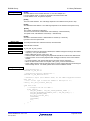
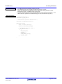
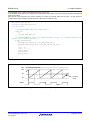
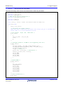
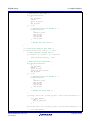
1. Introduction
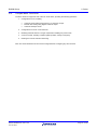
1. Introduction
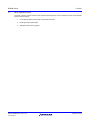
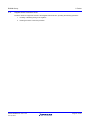
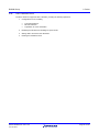
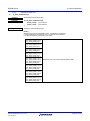
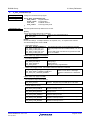
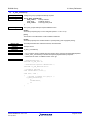
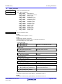
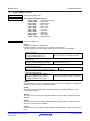
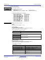
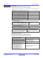
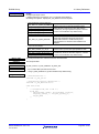
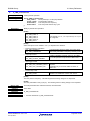
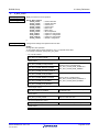
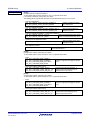
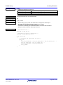
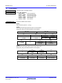
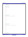
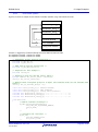
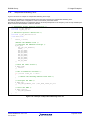
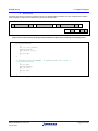
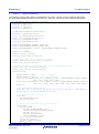
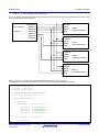
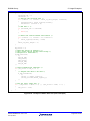
The Renesas Peripheral Driver Library (RPDL) is a unified API for controlling the peripheral modules on the microcontrollers
made by Renesas Electronics.
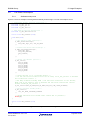
Callback functions
User application
Renesas Peripheral Driver Library
CPU
Peripherals supported by the RPDL
Target MCU
Figure 1-1: System configuration, with all peripherals supported by RPDL
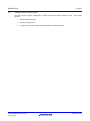
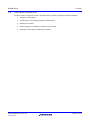
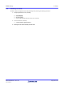
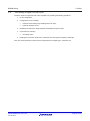
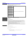
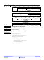
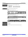
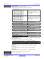
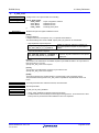
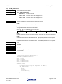
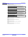
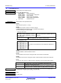
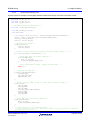
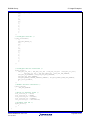
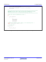
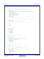
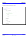
Callback functions
User application
Renesas Peripheral Driver Library
CPU
Peripherals supported by the RPDL
Middleware, including drivers
USB, Ethernet or CAN
Target MCU
Figure 1-2: System configuration, with middleware taking direct control of some peripherals
The library is packaged as:
a) A binary file containing all of the peripheral driver functions,
b) Header files containing the information that the user needs to call any of the functions from their own application
code and
c) Interrupt handlers supplied as source code.
For best use of this library, it is required that the user will have the following documents as a minimum:
i.
The hardware schematic diagram
ii.
The MCU hardware manual
iii.
This RPDL API User’s manual
The binary file is produced using the Renesas RX C tool chain. It should be usable by another linker that conforms to the
Renesas Application Binary Interface.
The coding standards and naming conventions are specified by Renesas.
R20UT1963EE0100 Rev.1.00
Jul 19, 2012
Page 1 of 487
RX63N Group
1.1.
1. Introduction
Tool chain requirements
This RPDL library has been built and tested using the C/C++ Compiler Package for RX Family V.1.02 Release 00. It cannot
be used with older versions of the tool chain.
The latest version of the tool chain can be downloaded from the Renesas Web site (Home / Products / Software and Tools /
Coding Tools / C/C++ Compilers and Assemblers / C/C++ Compiler Package for RX Family /).
1.2.
Using the library within your project
The driver library can be used in two ways.
1.2.1.
Via the PDG graphical utility
PDG can be downloaded from www.renesas.com/pdg.
The directions for use of the PDG utility are given in the PDG manual.
1.2.2.
Added to a project by the user and used stand-alone
To add the driver library to your project’s build environment, you need to
a)
b)
c)
d)
Unzip the RPDL distribution.
Copy the required source, header and library files into your project folder.
Include the required source files.
Add the driver library file to the linked files list.
The instructions to follow for stand-alone use start are given below.
1)
Unzip the RPDL files
Double-click on the file RPDL_RX63N.exe to unpack the files.
The default location is C:\Renesas\RPDL_RX63N.
2)
Copy the files into your project area
Navigate to where the RPDL files were unpacked.
Double-click on “Copy_RPDL_RX63N.bat” to start the copy process.
R20UT1963EE0100 Rev.1.00
Jul 19, 2012
Page 2 of 487
RX63N Group
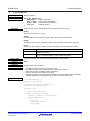
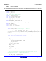
1. Introduction
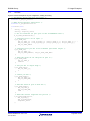
Select the device package option by pressing a number, and then press Enter.
Type the full path to the folder where you wish RPDL to be copied to, and then press Enter.
The utility will create a folder in the location that you specified and copy the files into the new folder.
R20UT1963EE0100 Rev.1.00
Jul 19, 2012
Page 3 of 487
RX63N Group
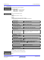
1. Introduction
Press any key to close the window.
R20UT1963EE0100 Rev.1.00
Jul 19, 2012
Page 4 of 487
RX63N Group
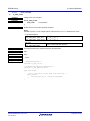
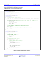
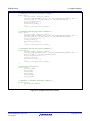
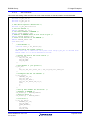
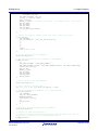
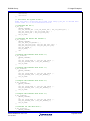
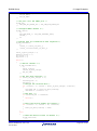
3)
1. Introduction
Include the new directory
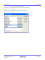
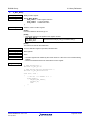
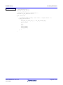
Use the key sequence Alt, B, R to open the “RX Standard Toolchain” window.
Select the C/C++ tab.
Use the key sequence S, I to show the included file directories.
Click on the “Add…” button.
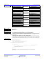
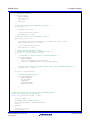
In the “Add include file directory” window, enter the details as shown:
Click on “OK” to close the window.
Click on the “Add…” button.
In the “Add include file directory” window, enter the details as shown:
Click on “OK” to close the window.
R20UT1963EE0100 Rev.1.00
Jul 19, 2012
Page 5 of 487
RX63N Group
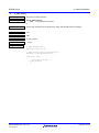
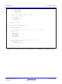
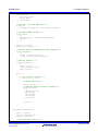
4)
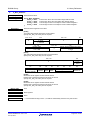
1. Introduction
Add the RPDL library file
The library file is added to the list used by the linker application.
Select the Link/Library tab.
From the “Show entries for :” drop-down menu, select “Library files”.
Click on the “Add…” button.
In the “Add library file” window, select “Project directory” and enter “RPDL\RX63N_library” as the File path.
Click on “OK” to close the window.
Click on “OK” to return to the main HEW window.
R20UT1963EE0100 Rev.1.00
Jul 19, 2012
Page 6 of 487
RX63N Group
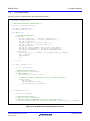
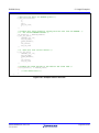
5)
1. Introduction
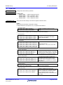
Include the new source files
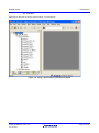
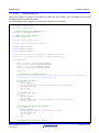
Use the key sequence Alt, P, A to open the “Add files to project ‘<your project>’” window.
Double click on the RPDL folder.
From the “Files of type” drop-down list, select “C source file (*.C)”.
Use the key sequence Ctrl-A to select all of the files, as shown below.
Click on “Add”.
Click on “OK” to return to the main HEW window.
R20UT1963EE0100 Rev.1.00
Jul 19, 2012
Page 7 of 487
RX63N Group
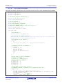
6)
1. Introduction
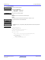
Peripherals that are not required
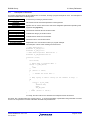
If a peripheral module is not required, the interrupt handler file does not need to be included.
If the unused interrupts still require entries in the interrupt vector table, edit the file Interrupt_not_RPDL.c to uncomment the
#define for the unused peripherals.
For example,
//#define RPDL_ADC_12_not_used
Becomes
#define RPDL_ADC_12_not_used
The file Interrupt_INTC.c must be included.
7)
Peripherals that are not supported by RPDL
The file Interrupt_not_RPDL.c also contains handlers for the peripherals that are not supported by RPDL. This allows the
user to add handler code for these peripherals while supporting the Fast Interrupt feature (see
R_INTC_CreateFastInterrupt).
R20UT1963EE0100 Rev.1.00
Jul 19, 2012
Page 8 of 487
RX63N Group
8)
1. Introduction
Avoid conflicts with standard project files
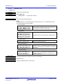
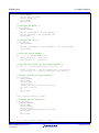
If the files ‘intprg.c’ or ‘vecttbl.c’ are included in the project, remove or exclude them.
(a) Removal
Use the key sequence Alt, P, R to open the “Remove Project Files” window.
Select the files and click on Remove.
R20UT1963EE0100 Rev.1.00
Jul 19, 2012
Page 9 of 487
RX63N Group
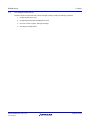
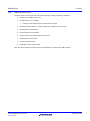
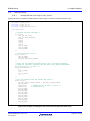
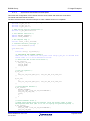
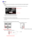
1. Introduction
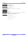
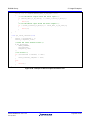
(b) Exclusion
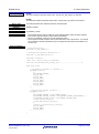
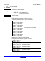
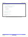
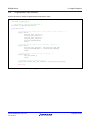
Select the two files and use the key sequence Alt, B, I to exclude them.
Figure 1-3: intprg.c and vecttbl.c have been excluded
R20UT1963EE0100 Rev.1.00
Jul 19, 2012
Page 10 of 487
RX63N Group
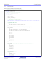
1. Introduction
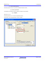
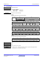
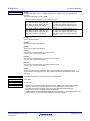
9) Set the build options.
Use the key sequence Alt, B, R to open the “RX Standard Toolchain” window.
(a) Set the optimisation
To avoid linking unused RPDL functions, adjust the Compiler and Linker settings.
(i)
Compiler
Select the C/C++ tab.
Use the key sequence Y, O, O to show the optimisation options.
Ensure that the “Inter-module optimization” option is enabled.
R20UT1963EE0100 Rev.1.00
Jul 19, 2012
Page 11 of 487
RX63N Group
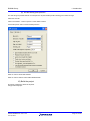
1. Introduction
(ii) Linker
Select the Link/Library tab.
Use the key sequence Y, O, O to show the optimisation options.
If the “Eliminate dead code” option is not enabled, from the Optimize drop-down list select Custom and enable the option.
R20UT1963EE0100 Rev.1.00
Jul 19, 2012
Page 12 of 487
RX63N Group
1. Introduction
(b) Set the floating point precision
The wide range of possible internal clock frequencies requires double-precision floating point number storage.
Select the CPU tab.
Click on the Details… button to open the “CPU details” window.
Use the drop-down menu to select Double precision.
Click on “OK” to close the window.
Click on “OK” to return to the main HEW window.
10) Build the project
No further configuration should be required.
Simply build the project.
R20UT1963EE0100 Rev.1.00
Jul 19, 2012
Page 13 of 487
RX63N Group
1.2.3.
1. Introduction
Header file inclusion
The RPDL folder contains a header file, iodefine_RPDL.h.
This file is included by the RPDL source files and will also be included by any user-generated files that call RPDL functions.
The main HEW project folder may contain the header file iodefine.h.
This file is normally used if access to the I/O registers in the MCU is required.
For any user-generated files that call RPDL functions, there is no need to include this file iodefine.h.
1.2.4.
Header file order
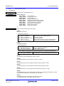
The file r_pdl_definitions.h must be included after any peripheral-specific header file.
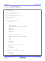
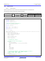
For example:
/* Peripheral driver function prototypes and definitions */
#include "r_pdl_cgc.h"
#include "r_pdl_cmt.h"
/* PDL device-specific definitions */
#include "r_pdl_definitions.h"
1.2.5.
Recommended initialisation code
The RX tool chain has a designated function for MCU initialisation, HardwareSetup().
During the MCU initialisation phase, it is recommended that the following functions are placed in this function.
Note that the file resetprg.c (supplied when a new project is created) requires editing to remove the “//” comment identifiers
for the two lines below.
//extern void HardwareSetup(void);
// HardwareSetup();
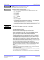
1) Initialisation of pins that are not available
For pins that are not available on the selected MCU package type, set the control registers to the recommended values using
R_IO_PORT_NotAvailable();
This function can be called even if the largest device has been selected. This will allow for the user’s code to be ported to
another project that does use a smaller MCU package.
2) Initialisation of the sub-clock oscillator if not used
If the sub-clock oscillator will not be used, it should be put into a stable state using the R_CGC_Control function.
/* Stop the sub-clock oscillator */
R_CGC_Control(
PDL_NO_DATA,
PDL_NO_DATA,
PDL_CGC_SUB_CLOCK_DISABLE
);
R20UT1963EE0100 Rev.1.00
Jul 19, 2012
Page 14 of 487
RX63N Group
1.3.
1. Introduction
Document structure
The drivers are summarised in section 2 and explained in detail in section 4.
Section 5 provides usage examples.
Section 6 provides details which are specific to the RX CPU.
R20UT1963EE0100 Rev.1.00
Jul 19, 2012
Page 15 of 487
RX63N Group
1.4.
1. Introduction
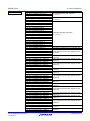
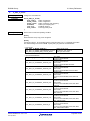
List of Abbreviations and Acronyms
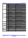
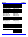
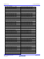
Abbreviation
ADC
API
BCD
Bit
bps
BSC
CAN
CGC
CMOS
CMT
CPU
CRC
DAC
DC
DMA
DMAC
DSP
DTC
EEPROM
EXDMA
EXDMAC
FIFO
GSM
HEW
HOCO
IEBus
I²C
INTC
I/O
IWDT
kB
LOCO
LPC
LSB
MB
MCU
MPC
MSB
MTU
NMI
OFS
PDG
PLL
POE
PPG
PWM
RAM
ROM
RPDL
RSPI
SCI
SDRAM
SMBus
SPI
USB
VGA
WDT
Analog to Digital Converter
Application Programming Interface
Binary-Coded Decimal
Binary digit
Bits per second
Bus State Controller
Controller Area Network
Clock Generation Circuit
Complementary Metal-Oxide Semiconductor
Compare Match Timer
Central Processing Unit
Cyclic Redundancy Check
Digital to Analog Converter
Direct Current
Direct Memory Access
DMA Controller
Digital Signal Processing
Data Transfer Controller
Electrically Erasable and Programmable ROM
External DMA
External DMAC
First-In, First-Out
Global System for Mobile communications
High-performance Embedded Workbench
High-speed On-Chip Oscillator
Inter-Equipment Bus
Inter-Integrated Circuit
Interrupt Controller
Input / Output
Independent WDT
Kilo Byte (1024 bytes)
Low-speed On-Chip Oscillator
Low Power Consumption
Least-Significant Bit
Mega Byte (1024 kB)
Microcontroller Unit
Multifunction Pin Controller
Most-Significant Bit
Multi-function Timer pulse Unit
Non-Maskable Interrupt
Option Function Select
Peripheral Driver Generator
Phase-Locked Loop
Port Output Enable
Programmable Pulse Generator
Pulse-Width Modulation
Random-Access Memory
Read-Only Memory
Renesas Peripheral Driver Library
Renesas SPI
Serial Communications Interface
Synchronous Dynamic RAM
System Management Bus
Serial Peripheral Interface
Universal Serial Bus
Video Graphics Array
Watchdog Timer
Full form
All trademarks and registered trademarks are the property of their respective owners.
R20UT1963EE0100 Rev.1.00
Jul 19, 2012
Page 16 of 487
RX63N Group
2. Driver
2. Driver
2.1.
Overview
This library provides a set of peripheral function control programs (peripheral drivers) for Renesas
microcontrollers and allows the peripheral driver to be built into a user program.
2.2.
Control Functions summary
This library has the following control functions available as peripheral drivers.
(1) Clock Generation Circuit
These driver functions are used to configure the multiple internal clock signals.
(2) Interrupt
These driver functions are used for configuring the external interrupt pins, handling fixed interrupts and controlling
the interrupt priority.
(3) I/O Port
These driver functions are used to configure the I/O pins and provide data read, write, compare and modify
operations.
(4) Port Function
These driver functions are used for configuring the I/O pin optional functions.
(5) MCU Operation
These driver functions are used for configuring the MCU operation.
(6) Low Power Consumption
These driver functions are used for selecting lower power consumption.
(7) Voltage Detection Circuit
These driver functions are used for configuring the low-voltage detection response.
(8) Bus Controller
These driver functions are used for configuring the external address bus, data bus and chip select pins and
handling any bus errors.
(9) DMA Controller
These driver functions are used for configuring and controlling the transfer of data within the address space.
(10) External DMA Controller
These driver functions are used for configuring and controlling the transfer of data within the address space.
(11) Data Transfer Controller
These driver functions are used for configuring and controlling the transfer of data triggered by peripheral
interrupts.
(12) Multi-Function Timer Pulse Unit
These driver functions are used for configuring and controlling the multi-function timers.
(13) Port Output Enable
These driver functions are used for additional configuring and controlling of the timer outputs.
(14) Programmable Pulse Generator
These driver functions are used for configuring and controlling the pulse generator outputs.
(15) 8-bit Timer
These driver functions are used for configuring and controlling the timers.
(16) Compare Match Timer
These driver functions are used for configuring and controlling the timers.
(17) Real-time Clock
These driver functions are used for configuring and controlling the real-time clock timer.
R20UT1963EE0100 Rev.1.00
Jul 19, 2012
Page 17 of 487
RX63N Group
2. Driver
(18) Watchdog Timer
These driver functions are used for configuring and controlling the timer.
(19) Independent Watchdog Timer
These driver functions are used for configuring and controlling the timer.
(20) Serial Communication Interface
These driver functions are used to configure the serial channels and manage the transmission and / or reception
of data across them.
(21) CRC calculator
These driver functions are used for controlling the calculator.
(22) I²C Bus Interface
These driver functions are used for controlling the I²C bus channels.
(23) Serial Peripheral Interface
These driver functions are used for controlling the SPI channels.
(24) 12-bit Analog to Digital Converter
These driver functions are used for configuring the 12-bit ADC units, controlling the units and reading the
conversion results.
(25) 10-bit Analog to Digital Converter
These driver functions are used for configuring the 10-bit ADC units, controlling the units and reading the
conversion results.
(26) 10-bit Digital to Analog converter
These driver functions are used for configuring the DAC module and setting the output voltages.
R20UT1963EE0100 Rev.1.00
Jul 19, 2012
Page 18 of 487
RX63N Group
2.3.
2. Driver
Clock Generation Circuit Driver
The driver functions support the control of the internal clock generator, providing the following operations.
1.
Configuration of the multiple clock outputs for system, peripheral and external bus operation.
2.
Controlling the clock generator operation.
3.
Reading the Clock generator status flags.
Note: Configuring the Clock Generation Circuit also provides information on clock frequencies that will be used by
the integrated drivers for other peripherals.
R20UT1963EE0100 Rev.1.00
Jul 19, 2012
Page 19 of 487
RX63N Group
2.4.
2. Driver
Interrupt Control Driver
The driver functions support the use of the interrupt controller, providing the following operations.
1.
Selecting the applicable interrupt pins.
2.
Configuration of an external interrupt signal for use.
3.
Enabling use of the software interrupt.
4.
Assigning an interrupt to be processed using the Fast Interrupt route.
5.
Assigning handlers for the fixed exception interrupts.
6.
Controlling an external interrupt input.
7.
Reading the status of an external interrupt.
8.
Reading an interrupt register.
9.
Writing to an interrupt register.
10. Modifying an interrupt register.
11. Configuring a group of interrupt sources.
12. Controlling a group of interrupt sources.
13. Reading the status of a group of interrupt sources.
14. Choosing the timer source for shared interrupts.
R20UT1963EE0100 Rev.1.00
Jul 19, 2012
Page 20 of 487
RX63N Group
2.5.
2. Driver
I/O Port Driver
The driver functions support the use of the I/O port pins, providing the following operations.
1.
Configuration for use.
2.
Reading the pin or port configuration.
3.
Modifying the pin or port configuration.
4.
Reading a pin or 8-bit port value.
5.
Writing to a pin or 8-bit port.
6.
Comparing a pin or 8-bit port with a supplied value.
7.
Modifying a pin or 8-bit port using a logical operation.
8.
Waiting until a pin or 8-bit port matches a supplied value.
9.
Configuring the pins that are not available on smaller packages to the required state.
R20UT1963EE0100 Rev.1.00
Jul 19, 2012
Page 21 of 487
RX63N Group
2.6.
2. Driver
Multifunction Pin Controller Driver
The driver functions support access to the Multifunction Pin Controller (MPC) registers which select the mode of
operation for some I/O pins.
The other driver functions modify the MPC registers automatically. For peripherals that are not supported by the
driver library, these functions support:
1.
Reading from an MPC register.
2.
Writing to an MPC register.
3.
Modifying an MPC register
R20UT1963EE0100 Rev.1.00
Jul 19, 2012
Page 22 of 487
RX63N Group
2.7.
2. Driver
MCU Operation Driver
The driver functions support access to the registers which select the mode of operation for the microcontroller.
These functions support:
1.
Controlling the MCU features and on-chip ROM and RAM.
2.
Reading the MCU status flags.
3.
Setting the MCU start-up options.
R20UT1963EE0100 Rev.1.00
Jul 19, 2012
Page 23 of 487
RX63N Group
2.8.
2. Driver
Voltage Detection Circuit Driver
The driver function supports configuration of VDET1 and VDET2 voltage detection circuits.
supports:
1.
Setting voltage thresholds.
2.
Defining a voltage event.
3.
Configuring a reset when supply voltage drops below a voltage threshold.
R20UT1963EE0100 Rev.1.00
Jul 19, 2012
This function
Page 24 of 487
RX63N Group
2.9.
2. Driver
Frequency Measurement Circuit Driver
The driver functions support access to the registers which control the frequency measurement circuit. These
functions support:
1.
Selecting the reference clock for each measurement system.
R20UT1963EE0100 Rev.1.00
Jul 19, 2012
Page 25 of 487
RX63N Group
2.10.
2. Driver
Low Power Consumption Driver
The driver functions support access to the registers which select the lower power modes of operation for the
microcontroller. These functions support:
1.
Configuring the state while in standby mode, and the activity that can be used to resume operation.
2.
Selecting one of the low-power modes.
3.
Writing data to the backup memory area.
4.
Reading data from the backup memory area.
5.
Determining the cause of the exit from the lowest power mode.
R20UT1963EE0100 Rev.1.00
Jul 19, 2012
Page 26 of 487
RX63N Group
2.11.
2. Driver
Register Write Protection Driver
The driver functions support the control of the Register Write Protection, providing the following operations.
1.
Enabling or disabling writing to the registers.
2.
Reading the status of the write protection.
R20UT1963EE0100 Rev.1.00
Jul 19, 2012
Page 27 of 487
RX63N Group
2.12.
2. Driver
Bus Controller Driver
The driver functions support the control of the external bus, providing the following operations.
1.
Setting the internal bus operation.
2.
Configuration of the controller.
3.
Configuration of the eight address space areas.
4.
Configuration of the SDRAM address space area.
5.
Disabling an area that is not required.
6.
Controlling the bus controller.
7.
Reading the status of the controller.
R20UT1963EE0100 Rev.1.00
Jul 19, 2012
Page 28 of 487
RX63N Group
2.13.
2. Driver
DMA Controller Driver
The driver functions support the control of the Direct Memory Access (DMA) controller, providing the following
operations.
1.
Configuration for use, including
•
Access to all control bits.
•
Automatic interrupt control
2.
Disabling DMA channels that are no longer required and enabling low-power mode.
3.
Control of a channel.
4.
Reading the status and operation registers of a channel.
R20UT1963EE0100 Rev.1.00
Jul 19, 2012
Page 29 of 487
RX63N Group
2. Driver
2.14. External DMA Controller Driver
The driver functions support the control of the external bus Direct Memory Access controller
(EXDMAC), providing the following operations.
1. Selecting the pins to be used.
2. Configuration for use, including
• Access to all control bits.
• Automatic interrupt control
3. Disabling EXDMAC channels that are no longer required and enabling low-power mode.
4. Control of a channel.
5. Reading the status and operation registers of a channel.
R20UT1963EE0100 Rev.1.00
Jul 19, 2012
Page 30 of 487
RX63N Group
2.15.
2. Driver
Data Transfer Controller Driver
The driver functions support the control of the Data Transfer Controller, providing the following operations.
1.
Setting the central options.
2.
Configuration for use, including support for chain transfers.
3.
Disabling the controller.
4.
Starting, stopping or modifying the operation of the controller.
5.
Reading the status flags and data transfer registers.
R20UT1963EE0100 Rev.1.00
Jul 19, 2012
Page 31 of 487
RX63N Group
2.16.
2. Driver
Multi-Function Timer Pulse Unit Driver
The driver functions support the use of the six 16-bit timers, providing the following operations.
1.
Selection of the MTU pins for use.
2.
Configuration for use, including
•
Access to all control bits.
•
Automatic interrupt control
•
Automatic I/O pin configuration
3.
Disabling channels that are no longer required and enabling low-power mode.
4.
Control of a timer channel.
5.
Control of a timer unit.
6.
Reading the status flags and registers of a timer channel.
7.
Reading the status flags and registers of a timer unit.
Note: The Clock Generation Circuit must be configured before configuring any timer channel.
R20UT1963EE0100 Rev.1.00
Jul 19, 2012
Page 32 of 487
RX63N Group
2.17.
2. Driver
Port Output Enable Driver
The driver functions support the use of the Port Output module, providing the following operations.
1.
Configuring the pins for use.
2.
Configuring the interrupts and callback functions.
3.
Run-time control of outputs, interrupts and flags.
4.
Checking the module status.
R20UT1963EE0100 Rev.1.00
Jul 19, 2012
Page 33 of 487
RX63N Group
2.18.
2. Driver
Timer Pulse Unit Driver
The driver functions support the use of the twelve 16-bit timers, providing the following operations.
1. I/O pin configuration
2. Configuration for use, including
• Access to all control bits.
• Automatic interrupt control
3. Disabling channels that are no longer required and enabling low-power mode.
4. Control of a timer.
5. Reading the status and registers of a timer.
R20UT1963EE0100 Rev.1.00
Jul 19, 2012
Page 34 of 487
RX63N Group
2.19.
2. Driver
Programmable Pulse Generator Driver
The driver functions support the use of the pulse generator, providing the following operations.
1.
Configuring the generator for use.
2.
Disabling groups of outputs that are no longer required.
3.
Control of the generator during run-time.
R20UT1963EE0100 Rev.1.00
Jul 19, 2012
Page 35 of 487
RX63N Group
2.20.
2. Driver
8-bit Timer Driver
The driver functions support the use of the four 8-bit timers, providing the following operations.
1.
Selection of the TMR pins for use.
2.
Configuring a channel for use, using register values which have been determined elsewhere.
3.
Configuring two channels as a 16-bit pair, using register values which have been determined elsewhere.
4.
Configuration for as a periodic timer, including
•
•
•
5.
Automatic clock setting using frequency or period as an input.
Automatic pulse width setting, using pulse width or duty cycle as an input.
Automatic interrupt control
Configuration for as a one-shot timer, including
•
•
•
•
Automatic clock setting, using pulse width as an input
Automatic interrupt control
CPU sleep option
Automatic support for using two channels as a single 16-bit timer.
6.
Disabling channels that are no longer required and enabling low-power mode.
7.
Control of a single timer channel.
8.
Control of two timer channels when configured as one 16-bit channel.
9.
Control of channels in periodic mode, enabling pulse-width modulation (PWM) output.
10. Reading the registers of a single timer channel.
11. Reading the registers of a 16-bit timer channel pair.
Note: The Clock Generation Circuit must be configured before configuring any timer channel.
R20UT1963EE0100 Rev.1.00
Jul 19, 2012
Page 36 of 487
RX63N Group
2.21.
2. Driver
Compare Match Timer Driver
The driver functions support the use of the two 16-bit timers, providing the following operations.
1.
Configuration for use, including
•
•
•
Automatic clock setting using frequency or period as an input.
Manual clock setting using register values as inputs.
Automatic interrupt control
2.
Configuration for use as a one-shot timer.
3.
Disabling channels that are no longer required and enabling low-power mode.
4.
Control of a timer, including constant register updates, change of frequency.
5.
Reading the counter value and status flag.
Note: The Clock Generation Circuit must be configured before configuring any timer channel.
R20UT1963EE0100 Rev.1.00
Jul 19, 2012
Page 37 of 487
RX63N Group
2.22.
2. Driver
Real-time Clock Driver
The driver functions support the use of the real-time clock, providing the following operations.
1.
Configuring the clock for use, including
•
•
•
•
•
•
Count source selection.
Alarm configuration.
Optional day-of-week calculation.
12 or 24 hour mode selection.
Automatic alarm and periodic interrupt control.
Setup of capture pins.
2.
Disabling the clock.
3.
Control of the clock, including
•
•
•
4.
Changing the alarm settings.
Changing the current date or time.
Error adjustment.
Reading the clock status flags, current time and date, alarm time and date and any captured times.
R20UT1963EE0100 Rev.1.00
Jul 19, 2012
Page 38 of 487
RX63N Group
2.23.
2. Driver
Watchdog Timer Driver
The driver functions support the use of the watchdog timer, providing the following operations.
1.
Configuring the timer for use, including
•
•
•
•
2.
Control of the timer, including
•
3.
Clock selection.
Time-out period.
Window position.
Reset or NMI Interrupt selection when timer overflows.
Counter refresh to prevent timeout.
Reading the timer status including counter value.
R20UT1963EE0100 Rev.1.00
Jul 19, 2012
Page 39 of 487
RX63N Group
2.24.
2. Driver
Independent Watchdog Timer Driver
The driver functions support the use of the independent watchdog timer, providing the following operations.
1.
Configuring the timer for use.
2.
Refreshing the timer to prevent the reset operation.
3.
Reading the timer status and counter register.
R20UT1963EE0100 Rev.1.00
Jul 19, 2012
Page 40 of 487
RX63N Group
2.25.
2. Driver
Serial Communication Interface Driver
The driver functions support the use of the serial communication (SCI) channels providing the following
operations.
1.
Selection of the SCI pins for use.
2.
Configuration for use, including
•
•
•
•
Automatic baud rate clock calculations
Automatic interrupt control
Automatic I/O pin configuration
Supporting the following modes:
o Asynchronous
o Multi-Processor
o Clock Synchronous
o Smart Card Interface
o Simple IIC
o Simple SPI
3.
Disabling channels that are no longer required.
4.
Transmitting data, with polling or interrupt mode automatically selected.
5.
Receiving data, with polling or interrupt mode automatically selected.
6.
Transmitting and/or receiving data in SPI mode, with polling or interrupt mode automatically selected.
7.
Transmitting data in simple IIC mode, with polling or interrupt mode automatically selected.
8.
Receiving data in simple IIC mode, with polling or interrupt mode automatically selected.
9.
Transmitting the last byte of data in simple IIC mode.
10. Control the channel operation.
11. Reading the status flags.
Note: The Clock Generation Circuit must be configured before configuring any serial channel.
R20UT1963EE0100 Rev.1.00
Jul 19, 2012
Page 41 of 487
RX63N Group
2.26.
2. Driver
I²C Bus Interface Driver
The driver functions support the use of the I²C module, providing the following operations.
1.
Configuration for use, including
•
•
Automatic clock setting using transfer rate as an input.
Automatic interrupt control
2.
Disabling the module that is no longer required and enabling low-power mode.
3.
Transmitting data in Master mode.
4.
Receiving data in Master mode.
5.
Completing the reception of data in Master mode.
6.
Monitoring the bus and handling the reception of data in Slave mode.
7.
Transmitting data in Slave mode.
8.
Control of the unit, including bus lock-up recovery support.
9.
Reading the status of the module.
Note: The Clock Generation Circuit must be configured before configuring the I²C module.
R20UT1963EE0100 Rev.1.00
Jul 19, 2012
Page 42 of 487
RX63N Group
2.27.
2. Driver
Serial Peripheral Interface Driver
The driver functions support the use of the SPI channels, providing the following operations.
1.
Selection of the SPI pins for use.
2.
Configuration for use, including
•
Automatic clock setting using transfer rate as an input.
3.
Disabling channels that are no longer required and enabling low-power mode.
4.
Configuration of command sequence settings.
5.
Managing the transfer of data on the interface, including
•
•
Automatic interrupt control
Automatic DMAC / DTC control.
6.
Control of special modes such as loopback.
7.
Reading the status of a module.
Note: The Clock Generation Circuit must be configured before configuring any SPI channel.
R20UT1963EE0100 Rev.1.00
Jul 19, 2012
Page 43 of 487
RX63N Group
2.28.
2. Driver
IEBus Interface Driver
The driver functions support the use of the IEBus channel, providing the following operations.
1.
Selection of the IEBus pins for use.
2.
Configuration for use, including
•
Automatic clock setting using the transfer rate as an input.
3.
Disabling channels that are no longer required and enabling low-power mode.
4.
Sending data as a bus master.
5.
Receiving data as a bus master.
6.
Monitor the bus and receiving data as a bus slave.
7.
Sending data as a bus slave.
8.
Control of special modes.
9.
Reading the status of the module.
Note: The Clock Generation Circuit must be configured before configuring any IEBus channel.
R20UT1963EE0100 Rev.1.00
Jul 19, 2012
Page 44 of 487
RX63N Group
2.29.
2. Driver
CRC Calculator Driver
The driver functions support the CRC calculator, providing the following operations.
1.
Configuration for use, including
•
•
•
Polynomial selection.
Bit order selection.
Preparation for a new calculation.
2.
Disabling the calculator and enabling low-power mode.
3.
Writing data to be used for the calculation.
4.
Reading the calculation result.
R20UT1963EE0100 Rev.1.00
Jul 19, 2012
Page 45 of 487
RX63N Group
2.30.
2. Driver
12-bit Analog to Digital Converter Driver
The driver functions support the use of the 12-bit ADC unit, providing the following operations.
1.
Configuration for use, including
•
•
•
Automatic clock setting using sampling time as an input
Automatic interrupt control
Sampling time control
2.
Disabling the unit when no longer required and enabling low-power mode.
3.
Control the ADC unit, including
•
4.
CPU sleep option
Reading the conversion results, with support for polling or interrupts.
Note: The Clock Generation Circuit must be configured before configuring the ADC unit.
R20UT1963EE0100 Rev.1.00
Jul 19, 2012
Page 46 of 487
RX63N Group
2.31.
2. Driver
10-bit Analog to Digital Converter Driver
The driver functions support the use of the 10-bit ADC unit, providing the following operations.
1.
I/O pin configuration
2.
Configuration for use, including
•
•
Automatic clock setting using sampling time as an input.
Automatic interrupt control
3.
Disabling units that are no longer required and enabling low-power mode.
4.
Control the unit, including
•
5.
CPU sleep option
Reading the conversion results of the 10-bit ADC unit, with support for polling or interrupts.
Note: The Clock Generation Circuit must be configured before configuring any 10-bit ADC unit.
R20UT1963EE0100 Rev.1.00
Jul 19, 2012
Page 47 of 487
RX63N Group
2.32.
2. Driver
10-bit Digital to Analog Converter Driver
The driver functions support the use of the DAC module, providing the following operations.
1.
Configuring a channel for use, including
•
•
Data alignment
D/A A/D synchronous conversion
2.
Disabling channels that are no longer required and enabling low-power mode.
3.
Writing data to a channel.
R20UT1963EE0100 Rev.1.00
Jul 19, 2012
Page 48 of 487
RX63N Group
2.33.
2. Driver
Temperature Sensor Driver
The driver functions support the use of the Temperature Sensor module, providing the following operations.
1.
Configuring and enabling the Temperature Sensor.
2.
Disabling the Temperature Sensor and enabling low-power mode.
3.
Controlling the A/D conversion.
R20UT1963EE0100 Rev.1.00
Jul 19, 2012
Page 49 of 487
RX63N Group
3. Types and definitions
3. Types and definitions
3.1.
Data types
This section describes the data types used in this library. For details about the setting values, refer to the section “4.2
Description of Each API”.
The header files stdint.h and stdbool.h are included with the Renesas RX compiler.
Table 1: Data types
Type
bool
double
uint8_t
uint16_t
int32_t
uint32_t
Defined in
stdbool.h
C
3.2.
General definitions
stdint.h
3.2.1.
Description
Boolean
Floating point, 64 bits
Unsigned, 8 bits
Unsigned, 16 bits
Signed, 32 bits
Unsigned, 32 bits
Range
0 (false) to 1 (true)
±∞
0 to 255
15
0 to 2 - 1
31
31
-2 to 2 - 1
32
0 to 2 - 1
PDL_NO_FUNC
Used as a parameter when there is no applicable function.
3.2.2.
PDL_NO_PTR
Used as a parameter when there is no applicable data location.
3.2.3.
PDL_NO_DATA
Used as a parameter when there is no applicable data value.
3.2.4.
PDL_MCU_GROUP
The MCU group supported by this build of the driver library. It is defined as RX63N.
A usage example is:
#if PDL_MCU_GROUP != RX63N
#error "Wrong RPDL !"
#endif
3.2.5.
PDL_VERSION
The version number of the RPDL library. The number is stored in BCD format (xx.xx). For example, 0100h is v1.00.
A usage example is:
const uint16_t rpdl_version_number = PDL_VERSION;
3.2.6.
Bit definitions
The definitions BIT_n and INV_BIT_n, where n = 0 to 31, are available to the user.
R20UT1963EE0100 Rev.1.00
Jul 19, 2012
Page 50 of 487
RX63N Group
4. Library Reference
4. Library Reference
4.1.
API List by Peripheral Function
Table 4.1 lists the Renesas Embedded APIs by peripheral function.
Table 4.1 Renesas Embedded API List
Category
Clock
Generation
Circuit
Interrupt control
unit
I/O port
Multifunction Pin
Controller
MCU operation
Voltage
Detection Circuit
Frequency
Measurement
Circuit
Low Power
Consumption
Register Write
Protection
Bus Controller
Number
1
2
3
1
2
3
4
5
6
7
8
9
10
11
12
13
14
1
2
3
4
5
6
7
8
9
1
2
3
1
2
3
1
2
3
Name
R_CGC_Set
R_CGC_Control
R_CGC_GetStatus
R_INTC_SetExtInterrupt
R_INTC_CreateExtInterrupt
R_INTC_CreateSoftwareInterrupt
R_INTC_CreateFastInterrupt
R_INTC_CreateExceptionHandlers
R_INTC_ControlExtInterrupt
R_INTC_GetExtInterruptStatus
R_INTC_Read
R_INTC_Write
R_INTC_Modify
R_INTC_CreateGroup
R_INTC_ControlGroup
R_INTC_GetStatusGroup
R_INTC_Control
R_IO_PORT_Set
R_IO_PORT_ReadControl
R_IO_PORT_ModifyControl
R_IO_PORT_Read
R_IO_PORT_Write
R_IO_PORT_Compare
R_IO_PORT_Modify
R_IO_PORT_Wait
R_IO_PORT_NotAvailable
R_MPC_Read
R_MPC_Write
R_MPC_Modify
R_MCU_Control
R_MCU_GetStatus
R_MCU_OFS
R_LVD_Create
R_LVD_Control
R_LVD_GetStatus
Description
Configure the clock generation circuit.
Modify the clock generation circuit operation.
Read the status of the clock generation circuit.
Select the external interrupt pins.
Configure an external interrupt signal.
Enable use of the software interrupt.
Assign handlers for the fixed-vector interrupts.
Enable faster interrupt processing for one interrupt.
External interrupt control.
Read the external interrupt status.
Read an interrupt register.
Update an interrupt register.
Modify an interrupt register.
Configure an interrupt source group.
Control an interrupt source group.
Read the status of an interrupt source group.
Control the operation of the interrupt controller.
Configure an I/O port.
Read an I/O port’s control registers.
Modify an I/O port’s control registers.
Read data from an I/O port.
Write data to an I/O port.
Check the pin states on an I/O port.
Modify the pin states on an I/O port.
Wait for a match on an I/O port.
Configure I/O port pins that are not available.
Read a PFC register.
Write to a PFC register.
Modify a PFC register.
Control the operation of the MCU.
Read the MCU status.
Configure the device start-up operation.
Configure the voltage detection circuit.
Control the voltage detection circuit.
Check the status of the voltage detection module.
1
R_MCK_Control
Configure the frequency measurement circuit.
1
2
3
4
5
1
2
1
2
3
4
5
6
7
R_LPC_Create
R_LPC_Control
R_LPC_WriteBackup
R_LPC_ReadBackup
R_LPC_GetStatus
R_RWP_Control
R_RWP_GetStatus
R_BSC_Set
R_BSC_Create
R_BSC_CreateArea
R_BSC_Destroy
R_BSC_Control
R_BSC_SDRAM_CreateArea
R_BSC_GetStatus
Configure the MCU low power conditions.
Select a low power consumption mode.
Write to the Backup registers.
Read from the Backup registers.
Read the status flags.
Control register write protection.
Get the status of the register protection.
Configure the internal bus operation.
Configure the external bus controller.
Configure an external bus area.
Stop the Bus Controller.
Modify the External Bus Controller operation.
Configure the SDRAM area.
Read the External Bus Controller status flags.
R20UT1963EE0100 Rev.1.00
Jul 19, 2012
Page 51 of 487
RX63N Group
DMA Controller
External DMA
Controller
Data Transfer
Controller
Multi-function
Timer pulse unit
Port Output
Enable
16-bit Timer
Pulse Unit
Programmable
Pulse Generator
8-bit Timer
Compare Match
Timer
Real-time Clock
Watchdog Timer
Independent
Watchdog Timer
4. Library Reference
1
2
3
4
1
2
3
4
5
1
2
3
4
5
1
2
3
4
5
6
7
1
2
3
R_DMAC_Create
R_DMAC_Destroy
R_DMAC_Control
R_DMAC_GetStatus
R_EXDMAC_Set
R_EXDMAC_Create
R_EXDMAC_Destroy
R_EXDMAC_Control
R_EXDMAC_GetStatus
R_DTC_Set
R_DTC_Create
R_DTC_Destroy
R_DTC_Control
R_DTC_GetStatus
R_MTU2_Set
R_MTU2_Create
R_MTU2_Destroy
R_MTU2_ControlChannel
R_MTU2_ControlUnit
R_MTU2_ReadChannel
R_MTU2_ReadUnit
R_POE_Set
R_POE_Create
R_POE_Control
4
R_POE_GetStatus
1
2
3
4
5
1
2
3
1
2
3
4
5
6
7
8
9
10
11
1
2
3
4
5
1
2
3
R_TPU_Set
R_TPU_Create
R_TPU_Destroy
R_TPU_Control
R_TPU_Read
R_PPG_Create
R_PPG_Destroy
R_PPG_Control
R_TMR_Set
R_TMR_CreateChannel
R_TMR_CreateUnit
R_TMR_CreatePeriodic
R_TMR_CreateOneShot
R_TMR_Destroy
R_TMR_ControlChannel
R_TMR_ControlUnit
R_TMR_ControlPeriodic
R_TMR_ReadChannel
R_TMR_ReadUnit
R_CMT_Create
R_CMT_CreateOneShot
R_CMT_Destroy
R_CMT_Control
R_CMT_Read
R_RTC_Create
R_RTC_Destroy
R_RTC_Control
4
R_RTC_Read
1
2
3
1
2
3
R_WDT_Set
R_WDT_Control
R_WDT_Read
R_IWDT_Set
R_IWDT_Control
R_IWDT_Read
R20UT1963EE0100 Rev.1.00
Jul 19, 2012
Configure the DMA controller.
Disable a DMA channel.
Control the DMA controller.
Check the status of the DMA channel.
Configure the EXDMAC pins.
Configure the EXDMA controller.
Disable the EXDMA controller.
Control the EXDMA controller.
Check the status of an EXDMAC channel.
Set the Data Transfer Controller options.
Configure the DTC for a transfer.
Shutdown the Data Transfer Controller.
Control the Data Transfer Controller.
Check the status of the Data Transfer Controller.
Configure the Multi-function Timer Pulse Units.
Configure a MTU channel.
Disable a Multi-function Timer Pulse Unit.
Control an MTU channel.
Control a Multi-function Timer Pulse Unit.
Read from MTU channel registers.
Read from MTU registers.
Configure the Port Output Enable module.
Configure the Port Output Enable event handling.
Control the Port Output Enable module.
Check the status of the Port Output Enable
module.
Configure the Timer Pulse Unit pins.
Configure a Timer Pulse Unit channel.
Disable a timer unit.
Control a timer channel.
Read from timer channel registers.
Configure a PPG group
Disable PPG outputs.
Control a PPG group.
Configure the optional TMR pins.
Configure a TMR timer channel.
Configure a TMR timer unit.
Select periodic operation.
Configure and use a one-shot timer.
Disable a TMR timer unit.
Write to timer channel registers.
Write to timer unit registers.
Control periodic operation.
Read from timer channel registers.
Read from timer unit registers.
Configure a CMT channel.
Configure a CMT channel as a one-shot event.
Disable a CMT unit.
Control CMT operation.
Read CMT channel status and registers.
Configure the Real-time clock.
Shut down the Real-time clock.
Modify the Real-time clock operation.
Read the Real-time clock status flags and
counters.
Configure the Watchdog timer operation.
Control the Watchdog operation.
Read the Watchdog timer status and registers.
Configure the Independent Watchdog operation.
Control the Independent Watchdog operation.
Read the watchdog timer status and counter.
Page 52 of 487
RX63N Group
Serial
Communication
Interface
I²C bus interface
Serial
Peripheral
Interface
IEBus Controller
CRC calculator
12-bit Analog to
Digital converter
10-bit Analog to
Digital converter
10-bit Digital to
Analog
converter
Temperature
sensor
4. Library Reference
1
2
3
4
5
6
7
8
9
10
11
1
2
3
4
5
6
7
8
9
1
2
3
4
5
6
7
1
2
3
4
5
6
7
8
9
1
2
3
4
1
2
3
4
1
2
3
4
5
1
2
3
R_SCI_Set
R_SCI_Create
R_SCI_Destroy
R_SCI_Send
R_SCI_Receive
R_SCI_SPI_Transfer
R_SCI_IIC_Write
R_SCI_IIC_Read
R_SCI_IIC_ReadLastByte
R_SCI_Control
R_SCI_GetStatus
R_IIC_Create
R_IIC_Destroy
R_IIC_MasterSend
R_IIC_MasterReceive
R_IIC_MasterReceiveLast
R_IIC_SlaveMonitor
R_IIC_SlaveSend
R_IIC_Control
R_IIC_GetStatus
R_SPI_Set
R_SPI_Create
R_SPI_Destroy
R_SPI_Command
R_SPI_Transfer
R_SPI_Control
R_SPI_GetStatus
R_IEB_Set
R_IEB_Create
R_IEB_Destroy
R_IEB_MasterSend
R_IEB_MasterReceive
R_IEB_SlaveMonitor
R_IEB_SlaveWrite
R_IEB_Control
R_IEB_GetStatus
R_CRC_Create
R_CRC_Destroy
R_CRC_Write
R_CRC_Read
R_ADC_12_Create
R_ADC_12_Destroy
R_ADC_12_Control
R_ADC_12_Read
R_ADC_10_Set
R_ADC_10_Create
R_ADC_10_Destroy
R_ADC_10_Control
R_ADC_10_Read
R_DAC_10_Create
R_DAC_10_Destroy
R_DAC_10_Write
Configure the SCI pin selection.
SCI channel setup.
Shut down a SCI channel.
Send a string of characters.
Receive a string of characters.
Perform an SCI SPI transfer.
Perform an SCI IIC master write.
Perform an SCI IIC master read.
Finish an SCI master read if using DMAC or DTC.
Control the SCI channel.
Check the status of an SCI channel.
I²C channel setup.
Disable an I²C channel.
Write data to a slave device.
Read data from a slave device.
Complete a DMAC or DTC-based read process.
Monitor the bus and receive data from a master.
Write data to a master device.
I²C channel control.
Read the status for an I²C channel.
Configure the SPI pin selection.
Configure an SPI channel.
Shutdown an SPI channel.
Configure an SPI command.
Transfer data over an SPI channel.
Control an SPI channel.
Check the status of an SPI channel.
Configure the IEBus pin selection.
Configure the IEBus channel.
Shutdown an IEBus channel.
Transmit data over an IEBus channel.
Receive data over an IEBus channel.
Monitor the IEBus.
Prepare data for sending to a master unit.
Change the IEBus channel configuration.
Check the status of an IEBus channel.
Configure the CRC calculator.
Shut down the CRC calculator.
Write data into the CRC calculation register.
Read the CRC calculation result.
Configure the 12-bit ADC unit.
Shut down the ADC unit.
Start or stop the ADC unit.
Read the ADC conversion results.
Select the I/O pins for 10-bit ADC.
Configure a 10-bit ADC unit.
Shut down an ADC unit.
Start or stop an ADC unit.
Read the ADC conversion results.
Configure the 10-bit DAC module.
Disable a DAC channel.
Write data to a DAC channel.
1
2
3
R_TS_Create
R_TS_Destroy
R_TS_Control
Configure the Temperature Sensor.
Shut down the Temperature Sensor.
Control the Temperature Sensor operation.
R20UT1963EE0100 Rev.1.00
Jul 19, 2012
Page 53 of 487
RX63N Group
4.2.
4. Library Reference
Description of Each API
This section describes each API and explains how to use them, showing a program example for each. The description of
each API is divided into the following items.
Synopsis
Summarises processing by the API function.
Prototype
The function format and a brief explanation of the arguments.
Description
Explains how to use the API function and shows assignable parameters separating each
argument with [argument].
Return value
Describes the returned value of the API function.
Category
Indicates the category of the API function.
Reference
Indicates the API functions to be referred.
Remark
Program example
Describes notes to use the API function.
Represents how to use the API function by a program example.
Two examples of return value checking are shown below.
/* RPDL definitions */
#include "r_pdl_mpc.h"
#include "r_pdl_sci.h"
/* RPDL device-specific definitions */
#include "r_pdl_definitions.h"
void func( void )
{
bool result;
/* Write 0xFF to register MPC1 */
result = R_MPC_Write(
1,
0xFF
);
if (result == false)
{
/* Handle the error here */
}
/* Keep trying to send a string (if the channel is busy) */
do
{
result = R_SCI_Send(
2,
"Renesas RX",
NULL,
PDL_NO_FUNC
);
} while (result == false);
}
For clarity, the return value is not checked in the examples used in this manual.
The RPDL API is implemented using function macros. To avoid the possibility of parameters being evaluated more than
once do not use operators or function calls within the RPDL API parameter list.
R20UT1963EE0100 Rev.1.00
Jul 19, 2012
Page 54 of 487
RX63N Group
4.2.1.
1)
4. Library Reference
Clock Generation Circuit
R_CGC_Set
Synopsis
Configure the clock generation circuit.
Prototype
bool R_CGC_Set(
uint8_t data1,
uint32_t data2,
double data3,
double data4,
double data5,
double data6,
double data7,
double data8,
double data9,
double data10
);
Description (1/2)
// Clock selection
// Configuration options
// Clock frequency
// System clock frequency
// Peripheral module clock A frequency
// Peripheral module clock B frequency
// Flash interface clock frequency
// External bus clock frequency
// IEBus clock frequency
// USB clock frequency
Set a clock source frequencies and options.
[data1]
Clock source selection.
• Clock source selection
PDL_CGC_CLK_LOCO or
PDL_CGC_CLK_HOCO or
PDL_CGC_CLK_MAIN or
PDL_CGC_CLK_SUB_CLOCK or
PDL_CGC_CLK_PLL or
PDL_CGC_CLK_IWDTLOCO
Select the low-speed on-chip oscillator (LOCO),
high-speed on-chip oscillator (HOCO),
main clock oscillator,
sub-clock oscillator,
Phase-locked loop (PLL) circuit or IWDT-dedicated
low-speed clock on-chip oscillator (IWDTLOCO).
[data2]
Configuration settings.
• BCLK signal control
PDL_CGC_BCLK_DIV_1 or
PDL_CGC_BCLK_DIV_2 or
PDL_CGC_BCLK_DISABLE
Select the BCLK or
BCLK ÷ 2 signal to be output or
disable the BCLK signal.
• SDCLK signal control (ignored if the device package does not support the external bus)
PDL_CGC_SDCLK_ENABLE or
Allow the SDRAM clock (SDCLK) signal to be output on
PDL_CGC_SDCLK_DISABLE
the SDCLK pin, or leave the SDCLK pin as an I/O port.
[data3]
The frequency of the selected clock source, in Hertz.
[data4]
The desired frequency of the System clock (ICLK), in Hertz.
[data5]
The desired frequency of the Peripheral module A clock (PCLKA), in Hertz.
[data6]
The desired frequency of the Peripheral module B clock (PCLKB), in Hertz.
[data7]
The desired frequency of the Flash memory interface clock (FCLK), in Hertz.
[data8]
The desired frequency of the External Bus clock (BCLK) and SDRAM clock (SDCLK), in Hertz.
If the external bus will not be used, specify PDL_NO_DATA.
[data9]
The desired frequency of the IEBus clock (IECLK), in Hertz.
If the IEBus will not be used, specify PDL_NO_DATA.
R20UT1963EE0100 Rev.1.00
Jul 19, 2012
Page 55 of 487
RX63N Group
Description (2/2)
Return value
Category
References
Remarks
4. Library Reference
[data10]
The desired frequency of the USB clock (UCLK), in Hertz.
If the USB will not be used, specify PDL_NO_DATA.
True if all parameters are valid and exclusive; otherwise false.
For RX63N, the following rules shall be checked:
•
fMAIN_CLOCK_OSCILLATOR ≤ 20 MHz (between 4 and 16 MHz if a resonator is used).
•
fPLL = 104 to 200 MHz
•
fICLK ≤ 100 MHz
•
fPCLKA ≤ 100 MHz
•
fPCLKB ≤ 50 MHz
•
fFCLK ≤ 50 MHz
•
fBCLK ≤ 100 MHz
•
fBCLK_PIN ≤ 50 MHz
•
fSDCLK_PIN ≤ 50 MHz
•
fBCLK ≤ fICLK
•
fIEBus_CLOCK ≤ 50 MHz
•
fUSB_CLOCK ≤ 48 MHz
•
The frequency of the PLL is achievable: (main clock) x 8, 10, 12, 16, 20, 24, 25 or 50.
•
The frequencies of the internal clocks (ICLK, PCLKA, PCLKB, FCLK and BCLK) are
achievable: (selected clock source) ÷ 1, 2, 4, 8, 16, 32 or 64.
•
The frequency of the IEBus clock (IECLK) is achievable: (selected clock source) ÷ 2, 4,
6, 8, 16, 32 or 64.
•
The frequency of the USB clock (UCLK) is achievable: (selected clock source) ÷ 3 or 4.
Clock generation circuit
R_CGC_Control, R_MCU_GetStatus, R_LPC_Create, R_BSC_Control
•
•
•
•
•
•
•
•
•
•
•
•
•
•
•
•
•
•
Call this function once for each clock source that will be used.
If the current clock source is selected in parameter data1, the frequencies of the internal
clocks will be changed by this function.
After a power-on reset, the MCU selects the LOCO as the clock source.
This function must be called before configuring clock-dependent modules.
This function will enable the selected clock but will not select it as the current clock source.
After the required settling time, use R_CGC_Control to select the desired clock source.
If the sub-clock is selected, the Start type status flag will be set to Warm (see
R_MCU_GetStatus).
If the sub-clock oscillator is not fitted, use R_CGC_Control to disable the oscillation circuit.
The registers MOSCWTCR (main clock), SOSCWTCR (sub-clock) and PLLWTCR (PLL)
provide stabilisation delays for the respective oscillator and must be written to while that
clock is stopped. If any of these registers needs to be modified, stop the clock (using
R_CGC_Control) and call R_LPC_Create to set the new value.
If the PLL will be used, first use this function to configure the main clock oscillator settings.
If the PLL will be used, the frequencies of the internal clocks (ICLK, PCLKA, PCLKB, FCLK
and BCLK) must be no more than the PLL output clock frequency ÷ 2.
If the main clock will be used, the frequencies of the internal clocks ICLK, PCLKA, PCLKB,
FCLK, BCLK and IECLK must be no more than the main clock frequency ÷ 4.
If the PLL output frequency is to be changed while the PLL is enabled, before calling this
function use R_CGC_Control to select another clock source and stop the PLL.
If the IWDTLOCO is selected, specify PDL_NO_DATA for parameters data2 and data4 to
data10.
The BCLK pin output will not be active until the external bus is enabled (using
R_BSC_Control).
The SDCLK pin output will not be active until the BSC functions are used to configure and
enable the SDRAM controller.
If the HOCO is selected, the HOCO power must not be turned off.
If the sub-clock will be selected while in low-speed operating mode 2 (see R_LPC_Create),
fICLK(Sub-clock) and fFCLK(Sub-clock) must equal fSUB-CLOCK.
If low-speed operating mode 1 or 2 is selected, do not call this function to configure the PLL.
R20UT1963EE0100 Rev.1.00
Jul 19, 2012
Page 56 of 487
RX63N Group
4. Library Reference
Program example
/* RPDL definitions */
#include "r_pdl_cgc.h"
/* RPDL device-specific definitions */
#include "r_pdl_definitions.h"
void func(void)
{
/* Configure main clock operation using a 12.0 MHz crystal */
/* ICLK = 3 MHz, PCLKA = 3 MHz, PCLKB = 3 MHz , FCLK = 3 MHz */
/* BCLK = IECLK = UCLK = not used, BCLK(pin) not used */
R_CGC_Set(
PDL_CGC_CLK_MAIN,
PDL_CGC_BCLK_DISABLE | PDL_CGC_SDCLK_DISABLE,
12E6,
3E6,
3E6,
3E6,
3E6,
PDL_NO_DATA,
PDL_NO_DATA,
PDL_NO_DATA
);
/* Configure PLL operation. The PLL will be set to 192 MHz */
/* ICLK = 96 MHz, PCLKA = 96 MHz, PCLKB = 48 MHz, FCLK = 48 MHz */
/* BCLK = 48 MHz, BCLK(pin) = 48 MHz. IECLK = UCLK = not used */
R_CGC_Set(
PDL_CGC_CLK_PLL,
PDL_CGC_BCLK_DIV_1 | PDL_CGC_SDCLK_ENABLE,
192E6,
96E6,
96E6,
48E6,
48E6,
48E6,
PDL_NO_DATA,
PDL_NO_DATA
);
}
R20UT1963EE0100 Rev.1.00
Jul 19, 2012
Page 57 of 487
RX63N Group
2)
4. Library Reference
R_CGC_Control
Synopsis
Modify the clock generation circuit operation.
Prototype
bool R_CGC_Control(
uint8_t data1,
// Clock selection
uint32_t data2, // Clock control options
uint8_t data3
// Clock control options
);
Description (1/2)
Modify the clock control registers.
[data1]
Clock source selection. If no change is required, specify PDL_NO_DATA.
• Clock source selection
PDL_CGC_CLK_LOCO or
PDL_CGC_CLK_HOCO or
PDL_CGC_CLK_MAIN or
PDL_CGC_CLK_SUB_CLOCK or
PDL_CGC_CLK_PLL
Select the low-speed on-chip oscillator (LOCO),
high-speed on-chip oscillator (HOCO),
main clock oscillator,
sub-clock oscillator,
Phase-locked loop (PLL) circuit.
[data2]
Clock control selection.
All selections are optional. If no change is required, specify PDL_NO_DATA.
If multiple selections are required, use “|” to separate each selection.
• BCLK pin output control (ignored if the device package does not support the external bus)
PDL_CGC_BCLK_ENABLE or
Enable or disable the BCLK pin output.
PDL_CGC_BCLK_DISABLE
• Low-speed on-chip oscillator control
PDL_CGC_LOCO_ENABLE or
PDL_CGC_LOCO_DISABLE
• High-speed on-chip oscillator control
PDL_CGC_HOCO_ENABLE or
PDL_CGC_HOCO_DISABLE
Enable or disable the LOCO.
Enable or disable the HOCO.
• High-speed on-chip oscillator power control
PDL_CGC_HOCO_POWER_ON or
Control the HOCO power supply.
PDL_CGC_HOCO_POWER_OFF
• Main clock oscillator control
PDL_CGC_MAIN_ENABLE or
PDL_CGC_MAIN_DISABLE
Enable or disable the main clock oscillator.
• Main clock oscillator forced oscillation control
PDL_CGC_MAIN_FORCED_ENABLE or Enable or disable forced oscillation of the main
PDL_CGC_MAIN_FORCED_DISABLE
clock oscillator.
• Main clock Oscillation Stop Detection control
PDL_CGC_OSC_STOP_ENABLE or
Enable (without or with interrupt request output)
PDL_CGC_OSC_STOP_INTERRUPT or or disable the oscillation stop detection function
PDL_CGC_OSC_STOP_DISABLE
for the main clock oscillator.
• Main clock Oscillation Stop Detection flag control
Clear the main clock oscillation stop detection
PDL_CGC_OSC_STOP_CLEAR_FLAG
flag.
• SDCLK signal control
PDL_CGC_SDCLK_ENABLE or
PDL_CGC_SDCLK_DISABLE
R20UT1963EE0100 Rev.1.00
Jul 19, 2012
Enable or disable the SDRAM clock (SDCLK)
signal.
Page 58 of 487
RX63N Group
Description (2/2)
4. Library Reference
[data3]
Clock control selection.
All selections are optional. If no change is required, specify PDL_NO_DATA.
If multiple selections are required, use “|” to separate each selection.
• Sub-clock oscillator control
PDL_CGC_SUB_CLOCK_ENABLE or
PDL_CGC_SUB_CLOCK_DISABLE
• PLL control
PDL_CGC_PLL_ENABLE or
PDL_CGC_PLL_DISABLE
Enable or disable the sub-clock oscillator.
Enable or disable the PLL circuit.
• IWDT-dedicated low-speed on-chip oscillator control
PDL_CGC_IWDTLOCO_ENABLE or
Enable or disable the IWDTLOCO.
PDL_CGC_IWDTLOCO_DISABLE
Return value
Category
References
Remarks
True if all parameters are valid and exclusive and a selected clock source has been configured;
otherwise false.
Clock generation circuit
R_CGC_Set, R_LPC_GetStatus, R_LPC_Create
•
•
•
•
•
•
•
•
•
•
•
•
Use R_CGC_Set to configure a clock source before selecting it.
While the main clock Oscillation Stop Detection feature is enabled, the LOCO is started and
cannot be stopped.
Clearing the main clock Oscillation Stop Detection flag will not succeed until a clock source
other than the main oscillator or PLL circuit is selected (using parameter data1).
If the main clock Oscillation Stop Detection flag is cleared, the interrupt output is also
disabled. Use this function to re-enable the interrupt output after the main clock oscillation
has been restored.
Do not stop a clock that is in use.
Do not change the clock source if an Operating Power Control Mode transition is taking
place (see R_LPC_GetStatus).
If low-speed operating mode 2 is selected (see R_LPC_Create), disable the HOCO.
If middle-speed operating modes 1 or 2 are selected (see R_LPC_Create), do not change
the HOCO power state.
If low-speed operating mode 1 or 2 is selected, do not enable the PLL.
If the main clock oscillator pins will be used as general I/O, call this function with
PDL_CGC_MAIN_DISABLE and PDL_CGC_MAIN_FORCED_DISABLE selected in
parameter data2.
If this function is used to enable a clock oscillator, wait for the required settling time before
selecting the clock source.
If the sub-clock oscillator is started after a power-on reset, the Start type status flag will be
set to Warm (see R_MCU_GetStatus).
R20UT1963EE0100 Rev.1.00
Jul 19, 2012
Page 59 of 487
RX63N Group
4. Library Reference
Program example
/* RPDL definitions */
#include "r_pdl_cgc.h"
/* RPDL device-specific definitions */
#include "r_pdl_definitions.h"
void func(void)
{
/* Stop the sub-clock oscillator */
R_CGC_Control(
PDL_NO_DATA,
PDL_NO_DATA,
PDL_CGC_SUB_CLOCK_DISABLE
);
/* Select the PLL */
R_CGC_Control(
PDL_CGC_CLK_PLL,
PDL_NO_DATA,
PDL_NO_DATA
);
}
R20UT1963EE0100 Rev.1.00
Jul 19, 2012
Page 60 of 487
RX63N Group
3)
4. Library Reference
R_CGC_GetStatus
Synopsis
Read the status of the clock generation circuit.
Prototype
bool R_CGC_GetStatus(
uint16_t * data // Pointer to the variable where the status value shall be stored.
);
Description
Read the clock status register.
[data]
The status flags shall be stored in the format below.
b15
0
b14
HOCO
power
0: Power on
1: Power off
b7
0
Return value
Category
References
Remarks
b13
b12
HOCO
IWDTLOCO
b6 - b4
Selected clock source
000b: LOCO
001b: HOCO
010b: Main clock
011b: Sub-clock
100b: PLL
b11
b10
Clock control
LOCO
Sub-clock
0: Operating
1: Stopped
b3 - b2
0
b9
b8
Main clock
PLL
b1
b0
Main clock oscillation stop detection
0: Disabled
1: Enabled
0: Normal operation
1: Stop detected
True.
Clock generation circuit
R_CGC_Control
•
Use R_CGC_Control to clear the main clock oscillation stop detection flag.
Program example
/* RPDL definitions */
#include "r_pdl_cgc.h"
/* RPDL device-specific definitions */
#include "r_pdl_definitions.h"
void func(void)
{
uint16_t Status_flags;
R_CGC_GetStatus(
&Status_flags
);
}
R20UT1963EE0100 Rev.1.00
Jul 19, 2012
Page 61 of 487
RX63N Group
4.2.2.
1)
4. Library Reference
Interrupt Control Unit
R_INTC_SetExtInterrupt
Synopsis
Select the external interrupt pins.
Prototype
bool R_INTC_SetExtInterrupt(
uint32_t data1, // Pin selection
uint32_t data2 // Pin selection
);
Description (1/2)
Assign the external interrupt pins.
[data1]
Allocate the pins for signals IRQ0 to IRQ7. All selections are optional.
If multiple selections are required, use “|” to separate each selection.
If no pins are required, specify PDL_NO_DATA.
PDL_INTC_IRQ0_P30 or
PDL_INTC_IRQ0_P10 or
PDL_INTC_IRQ0_PD0
PDL_INTC_IRQ1_P31 or
PDL_INTC_IRQ1_P11 or
PDL_INTC_IRQ1_PD1
PDL_INTC_IRQ2_P32 or
PDL_INTC_IRQ2_P12 or
PDL_INTC_IRQ2_PD2
PDL_INTC_IRQ3_P33 or
PDL_INTC_IRQ3_P13 or
PDL_INTC_IRQ3_PD3
PDL_INTC_IRQ4_PB1 or
PDL_INTC_IRQ4_P14 or
PDL_INTC_IRQ4_P34 or
PDL_INTC_IRQ4_PD4 or
PDL_INTC_IRQ4_PF5
PDL_INTC_IRQ5_PA4 or
PDL_INTC_IRQ5_P15 or
PDL_INTC_IRQ5_PD5 or
PDL_INTC_IRQ5_PE5
PDL_INTC_IRQ6_PA3 or
PDL_INTC_IRQ6_P16 or
PDL_INTC_IRQ6_PD6 or
PDL_INTC_IRQ6_PE6
PDL_INTC_IRQ7_PE2 or
PDL_INTC_IRQ7_P17 or
PDL_INTC_IRQ7_PD7 or
PDL_INTC_IRQ7_PE7
R20UT1963EE0100 Rev.1.00
Jul 19, 2012
Select the pins to be used for signals IRQ0 to IRQ7.
Page 62 of 487
RX63N Group
Description (2/2)
4. Library Reference
[data2]
Allocate the pins for signals IRQ8 to IRQ15. All selections are optional.
If multiple selections are required, use “|” to separate each selection.
If no pins are required, specify PDL_NO_DATA.
PDL_INTC_IRQ8_P40 or
PDL_INTC_IRQ8_P00 or
PDL_INTC_IRQ8_P20
PDL_INTC_IRQ9_P41 or
PDL_INTC_IRQ9_P01 or
PDL_INTC_IRQ9_P21
PDL_INTC_IRQ10_P42 or
PDL_INTC_IRQ10_P02 or
PDL_INTC_IRQ10_P55
PDL_INTC_IRQ11_P43 or
PDL_INTC_IRQ11_P03 or
PDL_INTC_IRQ11_PA1
PDL_INTC_IRQ12_P44 or
PDL_INTC_IRQ12_PB0 or
PDL_INTC_IRQ12_PC1
PDL_INTC_IRQ13_P45 or
PDL_INTC_IRQ13_P05 or
PDL_INTC_IRQ13_PC6
PDL_INTC_IRQ14_P46 or
PDL_INTC_IRQ14_PC0 or
PDL_INTC_IRQ14_PC7
PDL_INTC_IRQ15_P47 or
PDL_INTC_IRQ15_P07 or
PDL_INTC_IRQ15_P67
Return value
Category
References
Remarks
Select the pins to be used for signals IRQ8 to IRQ15.
True if all parameters are valid and exclusive; otherwise false.
Interrupt control
R_INTC_CreateExtInterrupt
• Before calling R_INTC_CreateExtInterrupt, call this function to select the required pins.
• The Multifunction Pin Control registers are modified to enable each selected IRQ pin and the
I/O Port PMR and PDR registers are modified to set the pin as an input.
• A pin can be used both as an interrupt input and a peripheral or general purpose input or
output (apart from an analog input). If the dual operation is required, call this function before
configuring the peripheral or I/O port operation.
• Some pin options are not available on smaller device packages.
• Some IRQ pins (labelled in the hardware manual with the suffix –DS) can also be used to exit
from Deep Software Standby mode. Please refer to the Low Power Consumption section for
details.
Program example
/* RPDL definitions */
#include "r_pdl_intc.h"
/* RPDL device-specific definitions */
#include "r_pdl_definitions.h"
void func(void)
{
/* Select P30 for IRQ0, P31 for IRQ1 and P42 for IRQ10 */
R_INTC_SetExtInterrupt(
PDL_INTC_IRQ0_PORT_3_0 | PDL_INTC_IRQ1_PORT_3_1,
PDL_INTC_IRQ10_PORT_4_2
);
}
R20UT1963EE0100 Rev.1.00
Jul 19, 2012
Page 63 of 487
RX63N Group
2)
4. Library Reference
R_INTC_CreateExtInterrupt
Synopsis
Configure an external interrupt signal.
Prototype
bool R_INTC_CreateExtInterrupt(
uint8_t data1,
// Signal selection
uint32_t data2, // Configuration
void * func,
// Callback function
uint8_t data3
// Interrupt priority level
);
Description (1/2)
Sets the specified interrupt detection and control.
[data1]
Choose the interrupt signal to be configured.
PDL_INTC_IRQn (n = 0 to 15) or
IRQn (n = 0 to 15) interrupt pin or
PDL_INTC_NMI
NMI.
[data2]
Choose the settings. If multiple selections are required, use “|” to separate each selection.
The default settings are shown in bold.
• Digital filter selection
PDL_INTC_FILTER_DISABLE or
PDL_INTC_FILTER_DIV_1 or
PDL_INTC_FILTER_DIV_8 or
PDL_INTC_FILTER_DIV_32 or
PDL_INTC_FILTER_DIV_64
The interrupt pin input can be unfiltered or sampled
using the peripheral clock PCLKB divided by 1, 8, 32 or
64.
For the NMI signal, this selection is ignored if the NMI
pin is not enabled.
Options which only apply to the IRQ pins
• Input sense selection
PDL_INTC_LOW or
PDL_INTC_FALLING or
PDL_INTC_RISING or
PDL_INTC_BOTH
Select Low level,
Falling edge,
Rising edge or
Falling and rising edge detection.
• DMAC / DTC trigger control. Not enabled if low-level detection is selected.
Disable or enable activation of the
PDL_INTC_DMAC_DTC_TRIGGER_DISABLE or
DMAC or DTC when a valid edge
PDL_INTC_DMAC_TRIGGER_ENABLE or
transition is detected on a valid IRQn
PDL_INTC_DTC_TRIGGER_ENABLE
pin.
Options which only apply to the NMI
• Pin enable and input sense selection
PDL_INTC_FALLING or
Enable the NMI pin and select falling or rising edge
PDL_INTC_RISING
detection. Required only if the NMI pin is to be used.
• Internal detection control
PDL_INTC_OSD_DISABLE or
PDL_INTC_OSD_ENABLE
PDL_INTC_WDT_DISABLE or
PDL_INTC_WDT_ENABLE
PDL_INTC_IWDT_DISABLE or
PDL_INTC_IWDT_ENABLE
PDL_INTC_LVD1_DISABLE or
PDL_INTC_LVD1_ENABLE
PDL_INTC_LVD2_DISABLE or
PDL_INTC_LVD2_ENABLE
R20UT1963EE0100 Rev.1.00
Jul 19, 2012
Disable or enable the NMI signal when the oscillation stop
detection interrupt occurs.
Disable or enable the NMI signal when a WDT underflow
interrupt occurs.
Disable or enable the NMI signal when an IWDT
underflow interrupt occurs.
Disable or enable the NMI signal when a low-voltage
detection 1 interrupt occurs.
Disable or enable the NMI signal when a low-voltage
detection 2 interrupt occurs.
Page 64 of 487
RX63N Group
Description (2/2)
4. Library Reference
[func]
The function to be called when a valid condition is detected.
Specify PDL_NO_FUNC if no IRQn interrupt is required.
A function must be specified for the NMI.
[data3]
The IRQn interrupt priority level. Select between 1 (lowest priority) and 15 (highest priority).
This parameter will be ignored if PDL_NO_FUNC is specified for parameter func.
This value does not apply to the NMI and is ignored.
Return value
True if all parameters are valid and exclusive; otherwise false.
Category
Interrupt control
Reference
R_INTC_SetExtInterrupt
Remarks
•
•
•
•
•
Function R_INTC_SetExtInterrupt must be called before any use of this function.
The selected interrupt is enabled automatically.
Please see the notes on callback function use in §6.
The NMI callback function should not return. It should stop operation or reset the system.
If the NMI interrupt fails to initialise, this function will return false.
Program example
/* RPDL definitions */
#include "r_pdl_intc.h"
/* RPDL device-specific definitions */
#include "r_pdl_definitions.h"
/* Callback function */
void CallBackFunc( void ){}
void func( void )
{
/* Configure the IRQ1 interrupt */
R_INTC_CreateExtInterrupt(
PDL_INTC_IRQ1,
PDL_INTC_FALLING,
CallBackFunc,
7
);
/* Configure the NMI pin */
R_INTC_CreateExtInterrupt(
PDL_INTC_NMI,
PDL_INTC_FALLING,
CallBackFunc,
15
);
/* Configure the NMI triggered by the WDT only (no NMI pin) */
R_INTC_CreateExtInterrupt(
PDL_INTC_NMI,
PDL_INTC_WDT_ENABLE,
CallBackFunc,
10
);
}
R20UT1963EE0100 Rev.1.00
Jul 19, 2012
Page 65 of 487
RX63N Group
3)
4. Library Reference
R_INTC_CreateSoftwareInterrupt
Synopsis
Enable use of the software interrupt.
Prototype
bool R_INTC_CreateSoftwareInterrupt(
uint8_t data1, // Configuration
void * func,
// Callback function
uint8_t data2 // Interrupt priority level
);
Description
Configure and enable the software interrupt.
[data1]
Choose the pin settings. The default setting is shown in bold.
• DTC trigger control.
PDL_INTC_DTC_SW_TRIGGER_DISABLE or
PDL_INTC_DTC_SW_TRIGGER_ENABLE
Disable or enable activation of the DTC
when a software interrupt is generated.
[func]
The function to be called when a valid condition is detected.
Specify PDL_NO_FUNC if no interrupt is required.
[data2]
The interrupt priority level. Select between 1 (lowest priority) and 15 (highest priority).
This parameter will be ignored if PDL_NO_FUNC is specified for parameter func.
Return value
True if all parameters are valid; otherwise false.
Category
Interrupt control
Reference
R_INTC_Write
Remarks
• Please see the notes on callback function use in §6.
• Specifying PDL_NO_FUNC for the callback function allows the software interrupt to be used
as a DTC trigger.
• Use R_INTC_Write to generate the software interrupt.
Program example
/* RPDL definitions */
#include "r_pdl_intc.h"
/* RPDL device-specific definitions */
#include "r_pdl_definitions.h"
/* Declaration of callback function */
void CallBackFunc( void );
void func( void )
{
/* Configure the software interrupt handler */
R_INTC_CreateSoftwareInterrupt(
PDL_NO_DATA,
CallBackFunc,
7
);
}
R20UT1963EE0100 Rev.1.00
Jul 19, 2012
Page 66 of 487
RX63N Group
4)
4. Library Reference
R_INTC_CreateFastInterrupt
Synopsis
Enable faster interrupt processing for one interrupt.
Prototype
bool R_INTC_CreateFastInterrupt(
uint8_t data
// The interrupt to be selected
);
Description (1/4)
[data]
Choose the interrupt vector to be processed using the fast interrupt process.
Name
Module
Interrupt cause
PDL_INTC_VECTOR_BUSERR
External bus
Error (illegal access or timeout)
PDL_INTC_VECTOR_FIFERR
Error
Flash memory
PDL_INTC_VECTOR_FRDYI
Ready
PDL_INTC_VECTOR_SWINT
Interrupt control Software interrupt
PDL_INTC_VECTOR_CMT0
PDL_INTC_VECTOR_CMT1
Compare match
Compare match
timer
PDL_INTC_VECTOR_CMT2
PDL_INTC_VECTOR_CMT3
PDL_INTC_VECTOR_EINT
Ethernet control Event detection
PDL_INTC_VECTOR_D0FIFO0
D0FIFO transfer request
PDL_INTC_VECTOR_D1FIFO0
D1FIFO transfer request
USB channel 0
PDL_INTC_VECTOR_USBI0
Event detection
PDL_INTC_VECTOR_USBR0
Resume
PDL_INTC_VECTOR_D0FIFO1
D0FIFO transfer request
PDL_INTC_VECTOR_D1FIFO1
D1FIFO transfer request
USB channel 1
PDL_INTC_VECTOR_USBI1
Event detection
PDL_INTC_VECTOR_USBR1
Resume
PDL_INTC_VECTOR_SPRI0
Receive buffer full
PDL_INTC_VECTOR_SPTI0
SPI channel 0
Transmit buffer empty
PDL_INTC_VECTOR_SPII0
Idle
PDL_INTC_VECTOR_SPRI1
Receive buffer full
PDL_INTC_VECTOR_SPTI1
SPI channel 1
Transmit buffer empty
PDL_INTC_VECTOR_SPII1
Idle
PDL_INTC_VECTOR_SPRI2
Receive buffer full
PDL_INTC_VECTOR_SPTI2
SPI channel 2
Transmit buffer empty
PDL_INTC_VECTOR_SPII2
Idle
PDL_INTC_VECTOR_RXF0
Receive FIFO
PDL_INTC_VECTOR_TXF0
Transmit FIFO
CAN channel 0
PDL_INTC_VECTOR_RXM0
Reception complete
PDL_INTC_VECTOR_TXM0
Transmission complete
PDL_INTC_VECTOR_RXF1
Receive FIFO
PDL_INTC_VECTOR_TXF1
Transmit FIFO
CAN channel 1
PDL_INTC_VECTOR_RXM1
Reception complete
PDL_INTC_VECTOR_TXM1
Transmission complete
PDL_INTC_VECTOR_RXF2
Receive FIFO
PDL_INTC_VECTOR_TXF2
Transmit FIFO
CAN channel 2
PDL_INTC_VECTOR_RXM2
Reception complete
PDL_INTC_VECTOR_TXM2
Transmission complete
PDL_INTC_VECTOR_CUP
Carry
PDL_INTC_VECTOR_ALM
Real-time clock
Alarm
PDL_INTC_VECTOR_PRD
Periodic
R20UT1963EE0100 Rev.1.00
Jul 19, 2012
Page 67 of 487
RX63N Group
Description (2/4)
4. Library Reference
PDL_INTC_VECTOR_IRQ0
PDL_INTC_VECTOR_IRQ1
PDL_INTC_VECTOR_IRQ2
PDL_INTC_VECTOR_IRQ3
PDL_INTC_VECTOR_IRQ4
PDL_INTC_VECTOR_IRQ5
PDL_INTC_VECTOR_IRQ6
PDL_INTC_VECTOR_IRQ7
PDL_INTC_VECTOR_IRQ8
PDL_INTC_VECTOR_IRQ9
PDL_INTC_VECTOR_IRQ10
PDL_INTC_VECTOR_IRQ11
PDL_INTC_VECTOR_IRQ12
PDL_INTC_VECTOR_IRQ13
PDL_INTC_VECTOR_IRQ14
PDL_INTC_VECTOR_IRQ15
PDL_INTC_VECTOR_GROUP0
PDL_INTC_VECTOR_GROUP1
PDL_INTC_VECTOR_GROUP2
PDL_INTC_VECTOR_GROUP3
PDL_INTC_VECTOR_GROUP4
PDL_INTC_VECTOR_GROUP5
PDL_INTC_VECTOR_GROUP6
PDL_INTC_VECTOR_GROUP12
PDL_INTC_VECTOR_ADI0
PDL_INTC_VECTOR_S12ADI0
PDL_INTC_VECTOR_SCIX0
PDL_INTC_VECTOR_SCIX1
PDL_INTC_VECTOR_SCIX2
PDL_INTC_VECTOR_SCIX3
PDL_INTC_VECTOR_TGI0A
PDL_INTC_VECTOR_TGI0B
PDL_INTC_VECTOR_TGI0C
PDL_INTC_VECTOR_TGI0D
PDL_INTC_VECTOR_TGI1A
PDL_INTC_VECTOR_TGI1B
PDL_INTC_VECTOR_TGI2A
PDL_INTC_VECTOR_TGI2B
PDL_INTC_VECTOR_TGI3A
PDL_INTC_VECTOR_TGI3B
PDL_INTC_VECTOR_TGI3C
PDL_INTC_VECTOR_TGI3D
PDL_INTC_VECTOR_TGI4A
PDL_INTC_VECTOR_TGI4B
PDL_INTC_VECTOR_TGI5A
PDL_INTC_VECTOR_TGI5B
PDL_INTC_VECTOR_TGI6A_A0
PDL_INTC_VECTOR_TGI6B_B0
PDL_INTC_VECTOR_TGI6C_C0
PDL_INTC_VECTOR_TGI6D_D0
PDL_INTC_VECTOR_TGIE0
PDL_INTC_VECTOR_TGIF0
PDL_INTC_VECTOR_TGI7A_A1
PDL_INTC_VECTOR_TGI7B_B1
PDL_INTC_VECTOR_TGI8A_A2
PDL_INTC_VECTOR_TGI8B_B2
R20UT1963EE0100 Rev.1.00
Jul 19, 2012
Valid edge or level detected on an
external interrupt pin
Interrupt
controller
10-bit ADC
12-bit ADC
SCI channel 12
Timer Pulse Unit
channel 0
Timer Pulse Unit
channel 1
Timer Pulse Unit
channel 2
Timer Pulse Unit
channel 3
Timer Pulse Unit
channel 4
Timer Pulse Unit
channel 5
Timer Pulse Unit
channel 6 or
Multi-function
Timer Pulse Unit
channel 0
Timer Pulse Unit
channel 7 or
Multi-function
Timer Pulse Unit
channel 1
Timer Pulse Unit
channel 8 or
Multi-function
Timer Pulse Unit
channel 2
Group 0 event
Group 1 event
Group 2 event
Group 3 event
Group 4 event
Group 5 event
Group 6 event
Group 12 event
Conversion completed
Conversion completed
Extended serial mode, Break field
Extended serial mode, Control field
Extended serial mode, Bus collision
Extended serial mode, Valid edge
Compare match or Input capture A
Compare match or Input capture B
Compare match or Input capture C
Compare match or Input capture D
Compare match or Input capture A
Compare match or Input capture B
Compare match or Input capture A
Compare match or Input capture B
Compare match or Input capture A
Compare match or Input capture B
Compare match or Input capture C
Compare match or Input capture D
Compare match or Input capture A
Compare match or Input capture B
Compare match or Input capture A
Compare match or Input capture B
Compare match or Input capture A
Compare match or Input capture B
Compare match or Input capture C
Compare match or Input capture D
Compare match E
Compare match F
Compare match or Input capture A
Compare match or Input capture B
Compare match or Input capture A
Compare match or Input capture B
Page 68 of 487
RX63N Group
Description (3/4)
4. Library Reference
PDL_INTC_VECTOR_TGIA3
PDL_INTC_VECTOR_TGIB3
PDL_INTC_VECTOR_TGIC3
PDL_INTC_VECTOR_TGID3
PDL_INTC_VECTOR_TGI10A_A4
PDL_INTC_VECTOR_TGI10B_B4
PDL_INTC_VECTOR_TGIC4
PDL_INTC_VECTOR_TGID4
PDL_INTC_VECTOR_TCIV4
PDL_INTC_VECTOR_TGIU5
PDL_INTC_VECTOR_TGIV5
PDL_INTC_VECTOR_TGIW5
PDL_INTC_VECTOR_TGI11A
PDL_INTC_VECTOR_TGI11B
PDL_INTC_VECTOR_OEI1
PDL_INTC_VECTOR_OEI2
PDL_INTC_VECTOR_CMIA0
PDL_INTC_VECTOR_CMIB0
PDL_INTC_VECTOR_OVI0
PDL_INTC_VECTOR_CMIA1
PDL_INTC_VECTOR_CMIB1
PDL_INTC_VECTOR_OVI1
PDL_INTC_VECTOR_CMIA2
PDL_INTC_VECTOR_CMIB2
PDL_INTC_VECTOR_OVI2
PDL_INTC_VECTOR_CMIA3
PDL_INTC_VECTOR_CMIB3
PDL_INTC_VECTOR_OVI3
PDL_INTC_VECTOR_ICEEI0
PDL_INTC_VECTOR_ICRXI0
PDL_INTC_VECTOR_ICTXI0
PDL_INTC_VECTOR_ICTEI0
PDL_INTC_VECTOR_ICEEI1
PDL_INTC_VECTOR_ICRXI1
PDL_INTC_VECTOR_ICTXI1
PDL_INTC_VECTOR_ICTEI1
PDL_INTC_VECTOR_ICEEI2
PDL_INTC_VECTOR_ICRXI2
PDL_INTC_VECTOR_ICTXI2
PDL_INTC_VECTOR_ICTEI2
PDL_INTC_VECTOR_ICEEI3
PDL_INTC_VECTOR_ICRXI3
PDL_INTC_VECTOR_ICTXI3
PDL_INTC_VECTOR_ICTEI3
PDL_INTC_VECTOR_DMAC0I
PDL_INTC_VECTOR_DMAC1I
PDL_INTC_VECTOR_DMAC2I
PDL_INTC_VECTOR_DMAC3I
PDL_INTC_VECTOR_EXDMAC0I
PDL_INTC_VECTOR_EXDMAC1I
PDL_INTC_VECTOR_RXI0
PDL_INTC_VECTOR_TXI0
PDL_INTC_VECTOR_TEI0
PDL_INTC_VECTOR_RXI1
PDL_INTC_VECTOR_TXI1
PDL_INTC_VECTOR_TEI1
PDL_INTC_VECTOR_RXI2
PDL_INTC_VECTOR_TXI2
PDL_INTC_VECTOR_TEI2
PDL_INTC_VECTOR_RXI3
PDL_INTC_VECTOR_TXI3
PDL_INTC_VECTOR_TEI3
R20UT1963EE0100 Rev.1.00
Jul 19, 2012
Timer Pulse Unit
channel 9 or
Multi-function
Timer Pulse Unit
channel 3
Timer Pulse Unit
channel 10 or
Multi-function
Timer Pulse Unit
channel 4
Timer Pulse Unit
channel 11 or
Multi-function
Timer Pulse Unit
channel 5
Port Output
Enable
8-bit timer TMR
channel 0
8-bit timer TMR
channel 1
8-bit timer TMR
channel 2
8-bit timer TMR
channel 3
I²C bus interface
channel 0
I²C bus interface
channel 1
I²C bus interface
channel 2
I²C bus interface
channel 3
Direct memory
access
controller
External DMAC
SCI channel 0
SCI channel 1
SCI channel 2
SCI channel 3
Compare match or Input capture A
Compare match or Input capture B
Compare match or Input capture C
Compare match or Input capture D
Compare match or Input capture A
Compare match or Input capture B
Compare match or Input capture C
Compare match or Input capture D
Overflow or underflow
Compare match or Input capture U
Compare match or Input capture V
Compare match or Input capture W
Compare match or Input capture A
Compare match or Input capture B
Input-level sampling or output-level
comparison detection
Compare match A
Compare match B
Overflow
Compare match A
Compare match B
Overflow
Compare match A
Compare match B
Overflow
Compare match A
Compare match B
Overflow
Transfer error or event generation
Data received
Start of next data transfer
End of data transfer
Transfer error or event generation
Data received
Start of next data transfer
End of data transfer
Transfer error or event generation
Data received
Start of next data transfer
End of data transfer
Transfer error or event generation
Data received
Start of next data transfer
End of data transfer
Transfer complete or Transfer
escape end
Transfer complete or Transfer
escape end
Data received
Start of next data transfer
End of data transfer
Data received
Start of next data transfer
End of data transfer
Data received
Start of next data transfer
End of data transfer
Data received
Start of next data transfer
End of data transfer
Page 69 of 487
RX63N Group
Description (4/4)
Return value
Category
4. Library Reference
PDL_INTC_VECTOR_RXI4
PDL_INTC_VECTOR_TXI4
PDL_INTC_VECTOR_TEI4
PDL_INTC_VECTOR_RXI5
PDL_INTC_VECTOR_TXI5
PDL_INTC_VECTOR_TEI5
PDL_INTC_VECTOR_RXI6
PDL_INTC_VECTOR_TXI6
PDL_INTC_VECTOR_TEI6
PDL_INTC_VECTOR_RXI7
PDL_INTC_VECTOR_TXI7
PDL_INTC_VECTOR_TEI7
PDL_INTC_VECTOR_RXI8
PDL_INTC_VECTOR_TXI8
PDL_INTC_VECTOR_TEI8
PDL_INTC_VECTOR_RXI9
PDL_INTC_VECTOR_TXI9
PDL_INTC_VECTOR_TEI9
PDL_INTC_VECTOR_RXI10
PDL_INTC_VECTOR_TXI10
PDL_INTC_VECTOR_TEI10
PDL_INTC_VECTOR_RXI11
PDL_INTC_VECTOR_TXI11
PDL_INTC_VECTOR_TEI11
PDL_INTC_VECTOR_RXI12
PDL_INTC_VECTOR_TXI12
PDL_INTC_VECTOR_TEI12
PDL_INTC_VECTOR_IEBINT
SCI channel 4
SCI channel 5
SCI channel 6
SCI channel 7
SCI channel 8
SCI channel 9
SCI channel 10
SCI channel 11
SCI channel 12
IEBus
Data received
Start of next data transfer
End of data transfer
Data received
Start of next data transfer
End of data transfer
Data received
Start of next data transfer
End of data transfer
Data received
Start of next data transfer
End of data transfer
Data received
Start of next data transfer
End of data transfer
Data received
Start of next data transfer
End of data transfer
Data received
Start of next data transfer
End of data transfer
Data received
Start of next data transfer
End of data transfer
Data received
Start of next data transfer
End of data transfer
Any enabled event
True.
Interrupt control
Reference
Remarks
• The fast interrupt processing is allocated to only one interrupt handler.
• Open the file r_pdl_user_definitions.h and edit the definition FAST_INTC_VECTOR to give it
the same value as the interrupt vector used in parameter data1.
For example:
#define FAST_INTC_VECTOR PDL_INTC_VECTOR_IRQ2
This will direct the compiler to generate the instructions required for a fast interrupt vector.
• This function uses an interrupt routine to modify the FINTV register. If the user has disabled
interrupts (cleared the ‘I’ bit in the PSW register) in their own code, this function will lock up.
Program example
/* RPDL definitions */
#include "r_pdl_intc.h"
/* RPDL device-specific definitions */
#include "r_pdl_definitions.h"
void func( void )
{
/* Assign the fast interrupt to the handler for pin IRQ3 */
R_INTC_CreateFastInterrupt(
PDL_INTC_VECTOR_IRQ3
);
}
/* Remember to edit r_pdl_user_definitions.h (see remark 2) */
R20UT1963EE0100 Rev.1.00
Jul 19, 2012
Page 70 of 487
RX63N Group
5)
4. Library Reference
R_INTC_CreateExceptionHandlers
Synopsis
Assign handlers for the fixed-vector interrupts.
Prototype
bool R_INTC_CreateExceptionHandlers(
void * func1,
// Callback function
void * func2,
// Callback function
void * func3,
// Callback function
void * func4
// Callback function
);
Description
Register the user functions to be called by the fixed-vector and software interrupts.
[func1]
The function to be called when a privileged instruction is detected while in user mode.
Specify PDL_NO_FUNC if no callback function is required.
[func2]
The function to be called when an access exception is detected.
Specify PDL_NO_FUNC if no callback function is required.
[func3]
The function to be called when an undefined instruction is detected.
Specify PDL_NO_FUNC if no callback function is required.
[func4]
The function to be called when a floating point exception is detected.
Specify PDL_NO_FUNC if no callback function is required.
Return value
Category
True.
Interrupt control
Reference
Remarks
• Please see the notes on callback function use in §6.
Program example
/* RPDL definitions */
#include "r_pdl_intc.h"
/* RPDL device-specific definitions */
#include "r_pdl_definitions.h"
/* Declaration of callback function */
void UndefinedInstruction( void );
void func( void )
{
/* Assign a function to manage undefined instruction errors */
R_INTC_CreateExceptionHandlers(
PDL_NO_FUNC,
PDL_NO_FUNC,
UndefinedInstruction,
PDL_NO_FUNC
);
}
R20UT1963EE0100 Rev.1.00
Jul 19, 2012
Page 71 of 487
RX63N Group
6)
4. Library Reference
R_INTC_ControlExtInterrupt
Synopsis
External interrupt control.
Prototype
bool R_INTC_ControlExtInterrupt(
uint8_t data1,
// Pin selection
uint32_t data2 // Control
);
Description
Modifies the specified external interrupt.
[data1]
Choose the interrupt pin to be controlled.
PDL_INTC_IRQn (n = 0 to 15) or
IRQn interrupt pin or
PDL_INTC_NMI
NMI interrupt pin
[data2]
Select the controls. If multiple selections are required, use “|” to separate each selection.
• Enable or disable the interrupt pin (for the IRQ pins)
PDL_INTC_ENABLE or
Enable or disable the IRQn interrupt pin.
PDL_INTC_DISABLE
• Digital filter selection
PDL_INTC_FILTER_DISABLE or
PDL_INTC_FILTER_DIV_1 or
PDL_INTC_FILTER_DIV_8 or
PDL_INTC_FILTER_DIV_32 or
PDL_INTC_FILTER_DIV_64
Disable the filter or select PCLKB divided by 1, 8, 32 or
64.
• Detection sense selection (for the IRQ pins)
PDL_INTC_LOW or
Select Low level,
PDL_INTC_FALLING or
Falling edge,
PDL_INTC_RISING or
Rising edge or
PDL_INTC_BOTH
Falling and rising edge detection.
• Interrupt request clearing
PDL_INTC_CLEAR_IR_FLAG
PDL_INTC_CLEAR_OSD_FLAG
PDL_INTC_CLEAR_WDT_FLAG
PDL_INTC_CLEAR_IWDT_FLAG
PDL_INTC_CLEAR_LVD1_FLAG
PDL_INTC_CLEAR_LVD2_FLAG
Return value
Clear the IRQ or NMI interrupt request flag.
This is not required if:
• A callback function has been specified.
• The interrupt priority level is higher than 0.
• The processor interrupt priority level is lower than
the interrupt priority level.
This operation should not be applied when low-level
detection is used.
Clear the Oscillation Stop detection NMI flag.
Clear the WDT event detection NMI flag.
Clear the IWDT event detection NMI flag.
Clear the LVD1 event detection NMI flag.
Clear the LVD2 event detection NMI flag.
True if all parameters are valid and exclusive; otherwise false.
Category
Interrupt control
Reference
R_INTC_CreateExtInterrupt, R_INTC_GetExtInterruptStatus
Remarks
• The NMI pin was enabled during R_INTC_CreateExtInterrupt and cannot be disabled (an
MCU design feature).
• When disabling an IRQn pin, the Interrupt Request flag will be cleared automatically.
• A callback function may be called once more if a valid event occurs just before the interrupt
pin is disabled.
R20UT1963EE0100 Rev.1.00
Jul 19, 2012
Page 72 of 487
RX63N Group
4. Library Reference
Program example
/* RPDL definitions */
#include "r_pdl_intc.h"
/* RPDL device-specific definitions */
#include "r_pdl_definitions.h"
void func( void )
{
/* Disable the IRQ1 interrupt pin and clear the flag */
R_INTC_ControlExtInterrupt(
PDL_INTC_IRQ1,
PDL_INTC_DISABLE | PDL_INTC_CLEAR_IR_FLAG
);
}
R20UT1963EE0100 Rev.1.00
Jul 19, 2012
Page 73 of 487
RX63N Group
7)
4. Library Reference
R_INTC_GetExtInterruptStatus
Synopsis
Read the external interrupt status.
Prototype
bool R_INTC_GetExtInterruptStatus(
uint8_t data1,
// Pin selection
uint8_t * data2 // A pointer to the buffer where the status data shall be stored.
);
Description
Acquire the status for the specified external interrupt.
[data1]
Choose the interrupt pin to be checked.
PDL_INTC_IRQn (n = 0 to 15) or
IRQn (n = 0 to 15) interrupt pin or
PDL_INTC_NMI
NMI interrupt pin
[data2]
The status flags shall be stored in the following format:
For an IRQ pin:
b7 – b4
0
b3 – b2
Detection condition
00: Low level
01: Falling edge
10: Rising edge
11: Both edges
For the NMI interrupt:
b7
b6
b5
b4
b3
Other interrupt request
Underflow
Oscillation
LVD2 LVD1
stop
IWDT
WDT
0: Not detected
1: Detected
Return value
b0
Status
0: Low
1: High
0: Not detected
1: Detected
b2
Current
level
0: Low
1: High
b1
b0
NMI pin
Detection
Request status
condition
0: Falling 0: Not detected
1: Rising
1: Detected
True if all parameters are valid and exclusive; otherwise false.
Category
Interrupt control
Reference
R_INTC_ControlExtInterrupt
Remarks
b1
Current level
• The MPC registers are used to determine which pin is used for IRQn.
• If this function is called from within a callback function, the input detection status will be 0.
• Clear the NMI status flags using R_INTC_ControlExtInterrupt.
Program example
/* RPDL definitions */
#include "r_pdl_intc.h"
/* RPDL device-specific definitions */
#include "r_pdl_definitions.h"
void func( void )
{
uint8_t irq_status;
/* Read the IR flag and pin state for IRQ5 */
R_INTC_GetExtInterruptStatus(
PDL_INTC_IRQ5,
&irq_status
);
}
R20UT1963EE0100 Rev.1.00
Jul 19, 2012
Page 74 of 487
RX63N Group
4. Library Reference
The INTC Read, Write and Modify functions use one of the following register definitions.
IR register definitions
PDL_INTC_REG_IR_BSC_BUSERR
PDL_INTC_REG_IR_FCU_FIFERR
PDL_INTC_REG_IR_FCU_FRDYI
PDL_INTC_REG_IR_ICU_SWINT
PDL_INTC_REG_IR_CMT0_CMI
PDL_INTC_REG_IR_CMT1_CMI
PDL_INTC_REG_IR_CMT2_CMI
PDL_INTC_REG_IR_CMT3_CMI
PDL_INTC_REG_IR_ETHER_EINT
PDL_INTC_REG_IR_USB0_D0FIFO
PDL_INTC_REG_IR_USB0_D1FIFO
PDL_INTC_REG_IR_USB0_USBI
PDL_INTC_REG_IR_USB1_D0FIFO
PDL_INTC_REG_IR_USB1_D1FIFO
PDL_INTC_REG_IR_USB1_USBI
PDL_INTC_REG_IR_SPI0_SPRI
PDL_INTC_REG_IR_SPI0_SPTI
PDL_INTC_REG_IR_SPI0_SPII
PDL_INTC_REG_IR_SPI1_SPRI
PDL_INTC_REG_IR_SPI1_SPTI
PDL_INTC_REG_IR_SPI1_SPII
PDL_INTC_REG_IR_SPI2_SPRI
PDL_INTC_REG_IR_SPI2_SPTI
PDL_INTC_REG_IR_SPI2_SPII
PDL_INTC_REG_IR_CAN0_RXF
PDL_INTC_REG_IR_CAN0_TXF
PDL_INTC_REG_IR_CAN0_RXM
PDL_INTC_REG_IR_CAN0_TXM
PDL_INTC_REG_IR_CAN1_RXF
PDL_INTC_REG_IR_CAN1_TXF
PDL_INTC_REG_IR_CAN1_RXM
PDL_INTC_REG_IR_CAN1_TXM
PDL_INTC_REG_IR_CAN2_RXF
PDL_INTC_REG_IR_CAN2_TXF
PDL_INTC_REG_IR_CAN2_RXM
PDL_INTC_REG_IR_CAN2_TXM
PDL_INTC_REG_IR_RTC_CUP
PDL_INTC_REG_IR_ICU_IRQ0
PDL_INTC_REG_IR_ICU_IRQ1
PDL_INTC_REG_IR_ICU_IRQ2
PDL_INTC_REG_IR_ICU_IRQ3
PDL_INTC_REG_IR_ICU_IRQ4
PDL_INTC_REG_IR_ICU_IRQ5
PDL_INTC_REG_IR_ICU_IRQ6
PDL_INTC_REG_IR_ICU_IRQ7
PDL_INTC_REG_IR_ICU_IRQ8
PDL_INTC_REG_IR_ICU_IRQ9
PDL_INTC_REG_IR_ICU_IRQ10
PDL_INTC_REG_IR_ICU_IRQ11
PDL_INTC_REG_IR_ICU_IRQ12
PDL_INTC_REG_IR_ICU_IRQ13
PDL_INTC_REG_IR_ICU_IRQ14
PDL_INTC_REG_IR_ICU_IRQ15
PDL_INTC_REG_IR_USB0_USBR
PDL_INTC_REG_IR_USB1_USBR
PDL_INTC_REG_IR_RTC_ALM
PDL_INTC_REG_IR_RTC_PRD
PDL_INTC_REG_IR_AD_ADI
PDL_INTC_REG_IR_S12AD_S12ADI
PDL_INTC_REG_IR_ICU_GROUP0
PDL_INTC_REG_IR_ICU_GROUP1
R20UT1963EE0100 Rev.1.00
Jul 19, 2012
PDL_INTC_REG_IR_ICU_GROUP2
PDL_INTC_REG_IR_ICU_GROUP3
PDL_INTC_REG_IR_ICU_GROUP4
PDL_INTC_REG_IR_ICU_GROUP5
PDL_INTC_REG_IR_ICU_GROUP6
PDL_INTC_REG_IR_ICU_GROUP12
PDL_INTC_REG_IR_SCI12_SCIX0
PDL_INTC_REG_IR_SCI12_SCIX1
PDL_INTC_REG_IR_SCI12_SCIX2
PDL_INTC_REG_IR_SCI12_SCIX3
PDL_INTC_REG_IR_TPU0_TGIA
PDL_INTC_REG_IR_TPU0_TGIB
PDL_INTC_REG_IR_TPU0_TGIC
PDL_INTC_REG_IR_TPU0_TGID
PDL_INTC_REG_IR_TPU1_TGIA
PDL_INTC_REG_IR_TPU1_TGIB
PDL_INTC_REG_IR_TPU2_TGIA
PDL_INTC_REG_IR_TPU2_TGIB
PDL_INTC_REG_IR_TPU3_TGIA
PDL_INTC_REG_IR_TPU3_TGIB
PDL_INTC_REG_IR_TPU3_TGIC
PDL_INTC_REG_IR_TPU3_TGID
PDL_INTC_REG_IR_TPU4_TGIA
PDL_INTC_REG_IR_TPU4_TGIB
PDL_INTC_REG_IR_TPU5_TGIA
PDL_INTC_REG_IR_TPU5_TGIB
PDL_INTC_REG_IR_TPU6_TGIA
PDL_INTC_REG_IR_TPU6_TGIB
PDL_INTC_REG_IR_TPU6_TGIC
PDL_INTC_REG_IR_TPU6_TGID
PDL_INTC_REG_IR_TPU7_TGIA
PDL_INTC_REG_IR_TPU7_TGIB
PDL_INTC_REG_IR_TPU8_TGIA
PDL_INTC_REG_IR_TPU8_TGIB
PDL_INTC_REG_IR_TPU9_TGIA
PDL_INTC_REG_IR_TPU9_TGIB
PDL_INTC_REG_IR_TPU9_TGIC
PDL_INTC_REG_IR_TPU9_TGID
PDL_INTC_REG_IR_TPU10_TGIA
PDL_INTC_REG_IR_TPU10_TGIB
PDL_INTC_REG_IR_TPU11_TGIA
PDL_INTC_REG_IR_TPU11_TGIB
PDL_INTC_REG_IR_MTU0_TGIA
PDL_INTC_REG_IR_MTU0_TGIB
PDL_INTC_REG_IR_MTU0_TGIC
PDL_INTC_REG_IR_MTU0_TGID
PDL_INTC_REG_IR_MTU0_TGIE
PDL_INTC_REG_IR_MTU0_TGIF
PDL_INTC_REG_IR_MTU1_TGIA
PDL_INTC_REG_IR_MTU1_TGIB
PDL_INTC_REG_IR_MTU2_TGIA
PDL_INTC_REG_IR_MTU2_TGIB
PDL_INTC_REG_IR_MTU3_TGIA
PDL_INTC_REG_IR_MTU3_TGIB
PDL_INTC_REG_IR_MTU3_TGIC
PDL_INTC_REG_IR_MTU3_TGID
PDL_INTC_REG_IR_MTU4_TGIA
PDL_INTC_REG_IR_MTU4_TGIB
PDL_INTC_REG_IR_MTU4_TGIC
PDL_INTC_REG_IR_MTU4_TGID
PDL_INTC_REG_IR_MTU4_TCIV
Page 75 of 487
RX63N Group
PDL_INTC_REG_IR_MTU5_TGIU
PDL_INTC_REG_IR_MTU5_TGIV
PDL_INTC_REG_IR_MTU5_TGIW
PDL_INTC_REG_IR_POE_OEI1
PDL_INTC_REG_IR_POE_OEI2
PDL_INTC_REG_IR_TMR0_CMIA
PDL_INTC_REG_IR_TMR0_CMIB
PDL_INTC_REG_IR_TMR0_OVI
PDL_INTC_REG_IR_TMR1_CMIA
PDL_INTC_REG_IR_TMR1_CMIB
PDL_INTC_REG_IR_TMR1_OVI
PDL_INTC_REG_IR_TMR2_CMIA
PDL_INTC_REG_IR_TMR2_CMIB
PDL_INTC_REG_IR_TMR2_OVI
PDL_INTC_REG_IR_TMR3_CMIA
PDL_INTC_REG_IR_TMR3_CMIB
PDL_INTC_REG_IR_TMR3_OVI
PDL_INTC_REG_IR_IIC0_EEI
PDL_INTC_REG_IR_IIC0_RXI
PDL_INTC_REG_IR_IIC0_TXI
PDL_INTC_REG_IR_IIC0_TEI
PDL_INTC_REG_IR_IIC1_EEI
PDL_INTC_REG_IR_IIC1_RXI
PDL_INTC_REG_IR_IIC1_TXI
PDL_INTC_REG_IR_IIC1_TEI
PDL_INTC_REG_IR_IIC2_EEI
PDL_INTC_REG_IR_IIC2_RXI
PDL_INTC_REG_IR_IIC2_TXI
PDL_INTC_REG_IR_IIC2_TEI
PDL_INTC_REG_IR_IIC3_EEI
PDL_INTC_REG_IR_IIC3_RXI
PDL_INTC_REG_IR_IIC3_TXI
PDL_INTC_REG_IR_IIC3_TEI
PDL_INTC_REG_IR_DMAC_DMAC0I
PDL_INTC_REG_IR_DMAC_DMAC1I
PDL_INTC_REG_IR_DMAC_DMAC2I
PDL_INTC_REG_IR_DMAC_DMAC3I
PDL_INTC_REG_IR_EXDMAC_EXDMAC0I
PDL_INTC_REG_IR_EXDMAC_EXDMAC1I
IER register definitions
PDL_INTC_REG_IER02
PDL_INTC_REG_IER03
PDL_INTC_REG_IER04
PDL_INTC_REG_IER05
PDL_INTC_REG_IER06
PDL_INTC_REG_IER07
PDL_INTC_REG_IER08
PDL_INTC_REG_IER09
PDL_INTC_REG_IER0B
PDL_INTC_REG_IER0C
PDL_INTC_REG_IER0D
PDL_INTC_REG_IER0E
PDL_INTC_REG_IER0F
PDL_INTC_REG_IER10
PDL_INTC_REG_IER11
R20UT1963EE0100 Rev.1.00
Jul 19, 2012
4. Library Reference
PDL_INTC_REG_IR_SCI0_RXI
PDL_INTC_REG_IR_SCI0_TXI
PDL_INTC_REG_IR_SCI0_TEI
PDL_INTC_REG_IR_SCI1_RXI
PDL_INTC_REG_IR_SCI1_TXI
PDL_INTC_REG_IR_SCI1_TEI
PDL_INTC_REG_IR_SCI2_RXI
PDL_INTC_REG_IR_SCI2_TXI
PDL_INTC_REG_IR_SCI2_TEI
PDL_INTC_REG_IR_SCI3_RXI
PDL_INTC_REG_IR_SCI3_TXI
PDL_INTC_REG_IR_SCI3_TEI
PDL_INTC_REG_IR_SCI4_RXI
PDL_INTC_REG_IR_SCI4_TXI
PDL_INTC_REG_IR_SCI4_TEI
PDL_INTC_REG_IR_SCI5_RXI
PDL_INTC_REG_IR_SCI5_TXI
PDL_INTC_REG_IR_SCI5_TEI
PDL_INTC_REG_IR_SCI6_RXI
PDL_INTC_REG_IR_SCI6_TXI
PDL_INTC_REG_IR_SCI6_TEI
PDL_INTC_REG_IR_SCI7_RXI
PDL_INTC_REG_IR_SCI7_TXI
PDL_INTC_REG_IR_SCI7_TEI
PDL_INTC_REG_IR_SCI8_RXI
PDL_INTC_REG_IR_SCI8_TXI
PDL_INTC_REG_IR_SCI8_TEI
PDL_INTC_REG_IR_SCI9_RXI
PDL_INTC_REG_IR_SCI9_TXI
PDL_INTC_REG_IR_SCI9_TEI
PDL_INTC_REG_IR_SCI10_RXI
PDL_INTC_REG_IR_SCI10_TXI
PDL_INTC_REG_IR_SCI10_TEI
PDL_INTC_REG_IR_SCI11_RXI
PDL_INTC_REG_IR_SCI11_TXI
PDL_INTC_REG_IR_SCI11_TEI
PDL_INTC_REG_IR_SCI12_RXI
PDL_INTC_REG_IR_SCI12_TXI
PDL_INTC_REG_IR_SCI12_TEI
PDL_INTC_REG_IR_IEB_IEBINT
PDL_INTC_REG_IER12
PDL_INTC_REG_IER13
PDL_INTC_REG_IER14
PDL_INTC_REG_IER15
PDL_INTC_REG_IER16
PDL_INTC_REG_IER17
PDL_INTC_REG_IER18
PDL_INTC_REG_IER19
PDL_INTC_REG_IER1A
PDL_INTC_REG_IER1B
PDL_INTC_REG_IER1C
PDL_INTC_REG_IER1D
PDL_INTC_REG_IER1E
PDL_INTC_REG_IER1F
Page 76 of 487
RX63N Group
IPR register definitions
PDL_INTC_REG_IPR_BSC_BUSERR
PDL_INTC_REG_IPR_FCU_FIFERR
PDL_INTC_REG_IPR_FCU_FRDYI
PDL_INTC_REG_IPR_ICU_SWINT
PDL_INTC_REG_IPR_CMT0_CMI
PDL_INTC_REG_IPR_CMT1_CMI
PDL_INTC_REG_IPR_CMT2_CMI
PDL_INTC_REG_IPR_CMT3_CMI
PDL_INTC_REG_IPR_ETHER_EINT
PDL_INTC_REG_IPR_USB0_D0FIFO
PDL_INTC_REG_IPR_USB0_D1FIFO
PDL_INTC_REG_IPR_USB0_USBI
PDL_INTC_REG_IPR_USB1_D0FIFO
PDL_INTC_REG_IPR_USB1_D1FIFO
PDL_INTC_REG_IPR_USB1_USBI
PDL_INTC_REG_IPR_SPI0
PDL_INTC_REG_IPR_SPI1
PDL_INTC_REG_IPR_SPI2
PDL_INTC_REG_IPR_CAN0
PDL_INTC_REG_IPR_CAN1
PDL_INTC_REG_IPR_CAN2
PDL_INTC_REG_IPR_RTC_CUP
PDL_INTC_REG_IPR_ICU_IRQ0
PDL_INTC_REG_IPR_ICU_IRQ1
PDL_INTC_REG_IPR_ICU_IRQ2
PDL_INTC_REG_IPR_ICU_IRQ3
PDL_INTC_REG_IPR_ICU_IRQ4
PDL_INTC_REG_IPR_ICU_IRQ5
PDL_INTC_REG_IPR_ICU_IRQ6
PDL_INTC_REG_IPR_ICU_IRQ7
PDL_INTC_REG_IPR_ICU_IRQ8
PDL_INTC_REG_IPR_ICU_IRQ9
PDL_INTC_REG_IPR_ICU_IRQ10
PDL_INTC_REG_IPR_ICU_IRQ11
PDL_INTC_REG_IPR_ICU_IRQ12
PDL_INTC_REG_IPR_ICU_IRQ13
PDL_INTC_REG_IPR_ICU_IRQ14
PDL_INTC_REG_IPR_ICU_IRQ15
PDL_INTC_REG_IPR_USB0_USBR
PDL_INTC_REG_IPR_USB1_USBR
PDL_INTC_REG_IPR_RTC_ALM
PDL_INTC_REG_IPR_RTC_PRD
PDL_INTC_REG_IPR_AD_ADI
PDL_INTC_REG_IPR_S12AD_S12ADI
PDL_INTC_REG_IPR_ICU_GROUP0
PDL_INTC_REG_IPR_ICU_GROUP1
PDL_INTC_REG_IPR_ICU_GROUP2
PDL_INTC_REG_IPR_ICU_GROUP3
PDL_INTC_REG_IPR_ICU_GROUP4
PDL_INTC_REG_IPR_ICU_GROUP5
PDL_INTC_REG_IPR_ICU_GROUP6
PDL_INTC_REG_IPR_ICU_GROUP12
PDL_INTC_REG_IPR_SCI12_SCIX
R20UT1963EE0100 Rev.1.00
Jul 19, 2012
4. Library Reference
PDL_INTC_REG_IPR_TPU0
PDL_INTC_REG_IPR_TPU1
PDL_INTC_REG_IPR_TPU2
PDL_INTC_REG_IPR_TPU3
PDL_INTC_REG_IPR_TPU4
PDL_INTC_REG_IPR_TPU5
PDL_INTC_REG_IPR_TPU6
PDL_INTC_REG_IPR_TPU7
PDL_INTC_REG_IPR_TPU8
PDL_INTC_REG_IPR_TPU9
PDL_INTC_REG_IPR_TPU10
PDL_INTC_REG_IPR_TPU11
PDL_INTC_REG_IPR_MTU0_TGIAD
PDL_INTC_REG_IPR_MTU0_TGIEF
PDL_INTC_REG_IPR_MTU1
PDL_INTC_REG_IPR_MTU2
PDL_INTC_REG_IPR_MTU3
PDL_INTC_REG_IPR_MTU4_TGIAD
PDL_INTC_REG_IPR_MTU4_TCIV
PDL_INTC_REG_IPR_MTU5
PDL_INTC_REG_IPR_POE
PDL_INTC_REG_IPR_TMR0
PDL_INTC_REG_IPR_TMR1
PDL_INTC_REG_IPR_TMR2
PDL_INTC_REG_IPR_TMR3
PDL_INTC_REG_IPR_IIC0_EEI
PDL_INTC_REG_IPR_IIC0_RXI
PDL_INTC_REG_IPR_IIC0_TXI
PDL_INTC_REG_IPR_IIC0_TEI
PDL_INTC_REG_IPR_IIC1_EEI
PDL_INTC_REG_IPR_IIC1_RXI
PDL_INTC_REG_IPR_IIC1_TXI
PDL_INTC_REG_IPR_IIC1_TEI
PDL_INTC_REG_IPR_IIC2_EEI
PDL_INTC_REG_IPR_IIC2_RXI
PDL_INTC_REG_IPR_IIC2_TXI
PDL_INTC_REG_IPR_IIC2_TEI
PDL_INTC_REG_IPR_IIC3_EEI
PDL_INTC_REG_IPR_IIC3_RXI
PDL_INTC_REG_IPR_IIC3_TXI
PDL_INTC_REG_IPR_IIC3_TEI
PDL_INTC_REG_IPR_DMAC_DMAC0I
PDL_INTC_REG_IPR_DMAC_DMAC1I
PDL_INTC_REG_IPR_DMAC_DMAC2I
PDL_INTC_REG_IPR_DMAC_DMAC3I
PDL_INTC_REG_IPR_EXDMAC_EXDMAC0I
PDL_INTC_REG_IPR_EXDMAC_EXDMAC1I
PDL_INTC_REG_IPR_SCI0
PDL_INTC_REG_IPR_SCI1
PDL_INTC_REG_IPR_SCI2
PDL_INTC_REG_IPR_SCI3
PDL_INTC_REG_IPR_SCI4
PDL_INTC_REG_IPR_SCI5
PDL_INTC_REG_IPR_SCI6
PDL_INTC_REG_IPR_SCI7
PDL_INTC_REG_IPR_SCI8
PDL_INTC_REG_IPR_SCI9
PDL_INTC_REG_IPR_SCI10
PDL_INTC_REG_IPR_SCI11
PDL_INTC_REG_IPR_SCI12
PDL_INTC_REG_IPR_IEB
Page 77 of 487
RX63N Group
DTCER register definitions
PDL_INTC_REG_DTCER_ICU_SWINT
PDL_INTC_REG_DTCER_CMT0_CMI
PDL_INTC_REG_DTCER_CMT1_CMI
PDL_INTC_REG_DTCER_CMT2_CMI
PDL_INTC_REG_DTCER_CMT3_CMI
PDL_INTC_REG_DTCER_USB0_D0FIFO
PDL_INTC_REG_DTCER_USB0_D1FIFO
PDL_INTC_REG_DTCER_USB1_D0FIFO
PDL_INTC_REG_DTCER_USB1_D1FIFO
PDL_INTC_REG_DTCER_SPI0_SPRI
PDL_INTC_REG_DTCER_SPI0_SPTI
PDL_INTC_REG_DTCER_SPI1_SPRI
PDL_INTC_REG_DTCER_SPI1_SPTI
PDL_INTC_REG_DTCER_SPI2_SPRI
PDL_INTC_REG_DTCER_SPI2_SPTI
PDL_INTC_REG_DTCER_ICU_IRQ0
PDL_INTC_REG_DTCER_ICU_IRQ1
PDL_INTC_REG_DTCER_ICU_IRQ2
PDL_INTC_REG_DTCER_ICU_IRQ3
PDL_INTC_REG_DTCER_ICU_IRQ4
PDL_INTC_REG_DTCER_ICU_IRQ5
PDL_INTC_REG_DTCER_ICU_IRQ6
PDL_INTC_REG_DTCER_ICU_IRQ7
PDL_INTC_REG_DTCER_ICU_IRQ8
PDL_INTC_REG_DTCER_ICU_IRQ9
PDL_INTC_REG_DTCER_ICU_IRQ10
PDL_INTC_REG_DTCER_ICU_IRQ11
PDL_INTC_REG_DTCER_ICU_IRQ12
PDL_INTC_REG_DTCER_ICU_IRQ13
PDL_INTC_REG_DTCER_ICU_IRQ14
PDL_INTC_REG_DTCER_ICU_IRQ15
PDL_INTC_REG_DTCER_AD_ADI
PDL_INTC_REG_DTCER_S12AD_S12ADI
PDL_INTC_REG_DTCER_TPU0_TGIA
PDL_INTC_REG_DTCER_TPU0_TGIB
PDL_INTC_REG_DTCER_TPU0_TGIC
PDL_INTC_REG_DTCER_TPU0_TGID
PDL_INTC_REG_DTCER_TPU1_TGIA
PDL_INTC_REG_DTCER_TPU1_TGIB
PDL_INTC_REG_DTCER_TPU2_TGIA
PDL_INTC_REG_DTCER_TPU2_TGIB
PDL_INTC_REG_DTCER_TPU3_TGIA
PDL_INTC_REG_DTCER_TPU3_TGIB
PDL_INTC_REG_DTCER_TPU3_TGIC
PDL_INTC_REG_DTCER_TPU3_TGID
PDL_INTC_REG_DTCER_TPU4_TGIA
PDL_INTC_REG_DTCER_TPU4_TGIB
PDL_INTC_REG_DTCER_TPU5_TGIA
PDL_INTC_REG_DTCER_TPU5_TGIB
PDL_INTC_REG_DTCER_TPU6_TGIA
PDL_INTC_REG_DTCER_TPU6_TGIB
PDL_INTC_REG_DTCER_TPU6_TGIC
PDL_INTC_REG_DTCER_TPU6_TGID
PDL_INTC_REG_DTCER_TPU7_TGIA
PDL_INTC_REG_DTCER_TPU7_TGIB
PDL_INTC_REG_DTCER_TPU8_TGIA
PDL_INTC_REG_DTCER_TPU8_TGIB
PDL_INTC_REG_DTCER_TPU9_TGIA
PDL_INTC_REG_DTCER_TPU9_TGIB
PDL_INTC_REG_DTCER_TPU9_TGIC
PDL_INTC_REG_DTCER_TPU9_TGID
PDL_INTC_REG_DTCER_TPU10_TGIA
PDL_INTC_REG_DTCER_TPU10_TGIB
R20UT1963EE0100 Rev.1.00
Jul 19, 2012
4. Library Reference
PDL_INTC_REG_DTCER_TPU11_TGIA
PDL_INTC_REG_DTCER_TPU11_TGIB
PDL_INTC_REG_DTCER_MTU0_TGIA
PDL_INTC_REG_DTCER_MTU0_TGIB
PDL_INTC_REG_DTCER_MTU0_TGIC
PDL_INTC_REG_DTCER_MTU0_TGID
PDL_INTC_REG_DTCER_MTU1_TGIA
PDL_INTC_REG_DTCER_MTU1_TGIB
PDL_INTC_REG_DTCER_MTU2_TGIA
PDL_INTC_REG_DTCER_MTU2_TGIB
PDL_INTC_REG_DTCER_MTU3_TGIA
PDL_INTC_REG_DTCER_MTU3_TGIB
PDL_INTC_REG_DTCER_MTU3_TGIC
PDL_INTC_REG_DTCER_MTU3_TGID
PDL_INTC_REG_DTCER_MTU4_TGIA
PDL_INTC_REG_DTCER_MTU4_TGIB
PDL_INTC_REG_DTCER_MTU4_TGIC
PDL_INTC_REG_DTCER_MTU4_TGID
PDL_INTC_REG_DTCER_MTU4_TCIV
PDL_INTC_REG_DTCER_MTU5_TGIU
PDL_INTC_REG_DTCER_MTU5_TGIV
PDL_INTC_REG_DTCER_MTU5_TGIW
PDL_INTC_REG_DTCER_TMR0_CMIA
PDL_INTC_REG_DTCER_TMR0_CMIB
PDL_INTC_REG_DTCER_TMR1_CMIA
PDL_INTC_REG_DTCER_TMR1_CMIB
PDL_INTC_REG_DTCER_TMR2_CMIA
PDL_INTC_REG_DTCER_TMR2_CMIB
PDL_INTC_REG_DTCER_TMR3_CMIA
PDL_INTC_REG_DTCER_TMR3_CMIB
PDL_INTC_REG_DTCER_IIC0_RXI
PDL_INTC_REG_DTCER_IIC0_TXI
PDL_INTC_REG_DTCER_IIC1_RXI
PDL_INTC_REG_DTCER_IIC1_TXI
PDL_INTC_REG_DTCER_IIC2_RXI
PDL_INTC_REG_DTCER_IIC2_TXI
PDL_INTC_REG_DTCER_IIC3_RXI
PDL_INTC_REG_DTCER_IIC3_TXI
PDL_INTC_REG_DTCER_DMAC_DMAC0I
PDL_INTC_REG_DTCER_DMAC_DMAC1I
PDL_INTC_REG_DTCER_DMAC_DMAC2I
PDL_INTC_REG_DTCER_DMAC_DMAC3I
PDL_INTC_REG_DTCER_EXDMAC_EXDMAC0I
PDL_INTC_REG_DTCER_EXDMAC_EXDMAC1I
PDL_INTC_REG_DTCER_SCI0_RXI
PDL_INTC_REG_DTCER_SCI0_TXI
PDL_INTC_REG_DTCER_SCI1_RXI
PDL_INTC_REG_DTCER_SCI1_TXI
PDL_INTC_REG_DTCER_SCI2_RXI
PDL_INTC_REG_DTCER_SCI2_TXI
PDL_INTC_REG_DTCER_SCI3_RXI
PDL_INTC_REG_DTCER_SCI3_TXI
PDL_INTC_REG_DTCER_SCI4_RXI
PDL_INTC_REG_DTCER_SCI4_TXI
PDL_INTC_REG_DTCER_SCI5_RXI
PDL_INTC_REG_DTCER_SCI5_TXI
PDL_INTC_REG_DTCER_SCI6_RXI
PDL_INTC_REG_DTCER_SCI6_TXI
PDL_INTC_REG_DTCER_SCI7_RXI
PDL_INTC_REG_DTCER_SCI7_TXI
PDL_INTC_REG_DTCER_SCI8_RXI
PDL_INTC_REG_DTCER_SCI8_TXI
Page 78 of 487
RX63N Group
PDL_INTC_REG_DTCER_SCI9_RXI
PDL_INTC_REG_DTCER_SCI9_TXI
PDL_INTC_REG_DTCER_SCI10_RXI
PDL_INTC_REG_DTCER_SCI10_TXI
R20UT1963EE0100 Rev.1.00
Jul 19, 2012
4. Library Reference
PDL_INTC_REG_DTCER_SCI11_RXI
PDL_INTC_REG_DTCER_SCI11_TXI
PDL_INTC_REG_DTCER_SCI12_RXI
PDL_INTC_REG_DTCER_SCI12_TXI
Page 79 of 487
RX63N Group
8)
4. Library Reference
R_INTC_Read
Synopsis
Read an interrupt register.
Prototype
bool R_INTC_Read(
uint16_t data1,
uint8_t * data2
);
Description
// Register selection
// Data storage location
Read an interrupt register and store the value.
[data1]
• The register to be read.
PDL_INTC_REG_IPL or
PDL_INTC_REG_IR_(register) or
PDL_INTC_REG_IER_(register) or
PDL_INTC_REG_IPR_(register) or
PDL_INTC_REG_DTCER_(register)
Select the current CPU interrupt priority level or
Interrupt Request register or
Interrupt Request Enable register or
Interrupt Priority register or
DTC Activation Enable register
[data2]
The location where the register’s value shall be stored.
Return value
True if all parameters are valid and exclusive; otherwise false.
Category
Interrupt control
Reference
None.
Remarks
• For (register), select one of the registers listed in the tables starting on page 75.
Program example
/* RPDL definitions */
#include "r_pdl_intc.h"
/* RPDL device-specific definitions */
#include "r_pdl_definitions.h"
void func( void )
{
uint8_t ipl;
/* Read the IPL bits */
R_INTC_Read(
PDL_INTC_REG_IPL,
&ipl
);
}
R20UT1963EE0100 Rev.1.00
Jul 19, 2012
Page 80 of 487
RX63N Group
9)
4. Library Reference
R_INTC_Write
Synopsis
Update an interrupt register.
Prototype
bool R_INTC_Write(
uint16_t data1,
uint8_t data2
);
Description
// Register selection
// Register value
Write the new value to an interrupt register.
[data1]
• The register to be updated.
PDL_INTC_REG_IPL or
PDL_INTC_REG_IR_(register) or
PDL_INTC_REG_IER_(register) or
PDL_INTC_REG_IPR_(register) or
PDL_INTC_REG_DTCER_(register) or
PDL_INTC_REG_SWINTR
Select the current CPU interrupt priority level or
Interrupt Request register or
Interrupt Request Enable register or
Interrupt Priority register or
DTC Activation Enable register or
Software interrupt activation register
[data2]
The value to be written to the register.
Return value
True if the parameter is within range; otherwise false.
Category
Interrupt control
Reference
None.
Remarks
• This function uses an interrupt routine to modify the IPL bits. If the user has disabled
interrupts (cleared the ‘I’ bit in the PSW register) in their own code, this function will lock up.
• For (register), select one of the registers listed in the tables starting on page 75.
• Write 1 to the SWINTR register to generate a software interrupt request.
Program example
/* RPDL definitions */
#include "r_pdl_intc.h"
/* RPDL device-specific definitions */
#include "r_pdl_definitions.h"
void func( void )
{
/* Set the IPL to 6 */
R_INTC_Write(
PDL_INTC_REG_IPL,
6
);
/* Set the IR for IRQ0 to 0 */
R_INTC_Write(
PDL_INTC_REG_IR_ICU_IRQ0,
0
);
}
R20UT1963EE0100 Rev.1.00
Jul 19, 2012
Page 81 of 487
RX63N Group
10)
4. Library Reference
R_INTC_Modify
Synopsis
Modify an interrupt register.
Prototype
bool R_INTC_Modify(
uint16_t data1, // Register selection
uint8_t data2,
// Logical operation
uint8_t data3
// Modification value
);
Description
Update the value in an interrupt register.
[data1]
• The register to be updated.
PDL_INTC_REG_IR_(register) or
PDL_INTC_REG_IER_(register) or
PDL_INTC_REG_IPR_(register)
Select the Interrupt Request register or
Interrupt Request Enable register or
Interrupt Priority register
[data2]
• The logical operation to be applied to the register contents.
PDL_INTC_AND or
PDL_INTC_OR or
Select between AND (&), OR (|) or Exclusive-OR (^).
PDL_INTC_XOR
[data3]
The value to be used by the logical operation.
Return value
True if the parameter is within range; otherwise false.
Category
Interrupt control
Reference
None.
Remarks
• This function uses an interrupt routine to modify the IPL bits. If the user has disabled
interrupts (cleared the ‘I’ bit in the PSW register) in their own code, this function will lock up.
• For (register), select one of the registers listed in the tables starting on page 75.
Program example
/* RPDL definitions */
#include "r_pdl_intc.h"
/* RPDL device-specific definitions */
#include "r_pdl_definitions.h"
void func( void )
{
/* Set bits 6 and 4 in IER09 to 1 */
R_INTC_Modify(
PDL_INTC_REG_IER09,
PDL_INTC_OR,
0x50
);
}
R20UT1963EE0100 Rev.1.00
Jul 19, 2012
Page 82 of 487
RX63N Group
11)
4. Library Reference
R_INTC_CreateGroup
Synopsis
Configure a group of peripheral interrupt requests.
Prototype
bool R_INTC_CreateGroup(
uint8_t data1,
// Group selection
void * func,
// Callback function
uint8_t data2
// Interrupt priority level
);
Description
Set up the grouped interrupt request callback function.
[data1]
The interrupt request group n to be configured (where n = 0 to 6 or 12).
[func]
The function to be called when a valid condition is detected.
[data2]
The interrupt priority level. Select between 1 (lowest priority) and 15 (highest priority).
Return value
True if all parameters are valid and exclusive; otherwise false.
Category
Interrupt control
Reference
R_INTC_ControlGroup
Remarks
• Do not use this function if RPDL functions will be used to configure the applicable peripheral.
• Use R_INTC_ControlGroup to enable the required peripheral interrupt requests.
• Please see the notes on callback function use in §6.
Program example
/* RPDL definitions */
#include "r_pdl_intc.h"
/* RPDL device-specific definitions */
#include "r_pdl_definitions.h"
/* Callback function */
void CallBackFunc( void ){}
void func( void )
{
/* Assign a handler for group 4 */
R_INTC_CreateGroup(
4,
CallBackFunc,
10
);
}
R20UT1963EE0100 Rev.1.00
Jul 19, 2012
Page 83 of 487
RX63N Group
12)
4. Library Reference
R_INTC_ControlGroup
Synopsis
Control an interrupt request group.
Prototype
bool R_INTC_ControlGroup(
uint8_t data1,
// Group selection
uint8_t data2,
// Interrupt control operation
uint32_t data3 // Interrupt source selection
);
Description (1/2)
Control an interrupt request group.
[data1]
The interrupt group n to be controlled (where n = 0 to 6 or 12).
[data2]
The logical operations to be applied to the interrupt request group.
If multiple selections are required, use “|” to separate each selection.
PDL_INTC_GROUP_DISABLE Disable the interrupt requests.
PDL_INTC_GROUP_CLEAR
Clear the interrupt request flags.
PDL_INTC_GROUP_ENABLE
Enable the interrupt requests.
[data3]
Choose the peripheral interrupt request sources (for the group specified in parameter data1) to
be modified.
If multiple selections are required, use “|” to separate each selection.
PDL_INTC_GRPn_ALL can be used to specify all applicable selections.
• Group 0 selections
PDL_INTC_GRP0_ERS0
PDL_INTC_GRP0_ERS1
PDL_INTC_GRP0_ERS2
• Group 1 selections
PDL_INTC_GRP1_TCIV0
PDL_INTC_GRP1_TCIV1
PDL_INTC_GRP1_TCIU1
• Group 2 selections
PDL_INTC_GRP2_TCIV2
PDL_INTC_GRP2_TCIU2
PDL_INTC_GRP2_TCIV3
• Group 3 selections
PDL_INTC_GRP3_TCI0V
PDL_INTC_GRP3_TCI1V
PDL_INTC_GRP3_TCI1U
PDL_INTC_GRP3_TCI5V
PDL_INTC_GRP3_TCI5U
• Group 4 selections
PDL_INTC_GRP4_TCI2V
PDL_INTC_GRP4_TCI2U
PDL_INTC_GRP4_TCI3V
PDL_INTC_GRP4_TCI4V
PDL_INTC_GRP4_TCI4U
• Group 5 selections
PDL_INTC_GRP5_TCI6V
PDL_INTC_GRP5_TCI7V
PDL_INTC_GRP5_TCI7U
PDL_INTC_GRP5_TCI11V
PDL_INTC_GRP5_TCI11U
R20UT1963EE0100 Rev.1.00
Jul 19, 2012
Error on CAN channels 0, 1 or 2.
Overflow on MTU channels 0 or 1.
Underflow on MTU channel 1.
Overflow on MTU channels 2 or 3.
Underflow on MTU channel 3.
Overflow on TPU channels 0, 1 or 5.
Underflow on TPU channels 1 or 5.
Overflow on TPU channels 2, 3 or 4.
Underflow on TPU channels 2 or 4.
Overflow on TPU channels 6, 7 or 11.
Underflow on TPU channels 7 or 11.
Page 84 of 487
RX63N Group
Description (2/2)
4. Library Reference
• Group 6 selections
PDL_INTC_GRP6_TCI8V
PDL_INTC_GRP6_TCI8U
PDL_INTC_GRP6_TCI9V
PDL_INTC_GRP6_TCI10V
PDL_INTC_GRP6_TCI10U
Overflow on TPU channels 8, 9 or 10.
Underflow on TPU channels 8 or 10.
• Group 12 selections. Flag clearing (using PDL_INTC_GROUP_CLEAR) is not possible.
PDL_INTC_GRP12_ERI0
PDL_INTC_GRP12_ERI1
PDL_INTC_GRP12_ERI2
PDL_INTC_GRP12_ERI3
PDL_INTC_GRP12_ERI4
PDL_INTC_GRP12_ERI5
PDL_INTC_GRP12_ERI6
Reception error on SCI channels 0 to 12.
PDL_INTC_GRP12_ERI7
PDL_INTC_GRP12_ERI8
PDL_INTC_GRP12_ERI9
PDL_INTC_GRP12_ERI10
PDL_INTC_GRP12_ERI11
PDL_INTC_GRP12_ERI12
PDL_INTC_GRP12_SPEI0
PDL_INTC_GRP12_SPEI1 SPI error on channels 0 to 2.
PDL_INTC_GRP12_SPEI2
Return value
False if the group number is invalid; otherwise true.
Category
Interrupt control
Reference
R_INTC_CreateGroup
Remarks
•
•
•
•
Do not use this function if RPDL functions will be used to control the applicable peripheral.
Call R_INTC_CreateGroup before calling this function.
Flag clearing is done after any interrupt disabling and before any interrupt enabling.
Group 12 interrupts use level detection, so clearing must be done by clearing the source of
the interrupt.
Program example
/* RPDL definitions */
#include "r_pdl_intc.h"
/* RPDL device-specific definitions */
#include "r_pdl_definitions.h"
void func( void )
{
/* Disable the interrupt for the overflow on MTU channel 0 and clear
the flag */
R_INTC_ControlGroup(
1,
PDL_INTC_GROUP_DISABLE | PDL_INTC_GROUP_CLEAR,
PDL_INTC_GRP1_TCIV0
);
/* Enable all of the Group 3 interrupt sources */
R_INTC_ControlGroup(
3,
PDL_INTC_GROUP_ENABLE,
PDL_INTC_GRP3_ALL
);
}
R20UT1963EE0100 Rev.1.00
Jul 19, 2012
Page 85 of 487
RX63N Group
13)
4. Library Reference
R_INTC_GetStatusGroup
Synopsis
Read the status of an interrupt request group.
Prototype
bool R_INTC_GetStatusGroup(
uint8_t data1,
// Group selection
uint32_t * data2 // Data storage location
);
Description (1/2)
Read the grouped interrupt request status flags.
[data1]
The interrupt request group n to be read (where n = 0 to 6 or 12).
[data2]
The status flags shall be stored in the format below.
• Group 0
b31 – b3
b2
b1
b0
CAN error interrupts
Channel 2 Channel 1 Channel 0
0: Not requested
1: Requested
0
• Group 1
b31 – b3
b2
b1
b0
MTU interrupts
Underflow on Overflow on Overflow on
channel 1
channel 1
channel 0
0: Not requested
1: Requested
0
• Group 2
b31 – b3
b2
b1
b0
MTU interrupts
Overflow on Underflow on Overflow on
channel 3
channel 2
channel 2
0: Not requested
1: Requested
0
• Group 3
b31 – b5
0
• Group 4
b31 – b5
0
• Group 5
b31 – b5
0
R20UT1963EE0100 Rev.1.00
Jul 19, 2012
b4
Underflow on
channel 5
b4
Underflow on
channel 4
b4
Underflow on
channel 11
b3
b2
b1
TPU interrupts
Overflow on Underflow on Overflow on
channel 5
channel 1
channel 1
0: Not requested
1: Requested
b3
b2
b1
TPU interrupts
Overflow on Overflow on Underflow on
channel 4
channel 3
channel 2
0: Not requested
1: Requested
b3
b2
b1
TPU interrupts
Overflow on Underflow on Overflow on
channel 11
channel 7
channel 7
0: Not requested
1: Requested
b0
Overflow on
channel 0
b0
Overflow on
channel 2
b0
Overflow on
channel 6
Page 86 of 487
RX63N Group
Description (2/2)
4. Library Reference
• Group 6
b31 – b5
b4
b3
b2
b1
TPU interrupts
Overflow on Overflow on Underflow on
channel 10
channel 9
channel 8
0: Not requested
1: Requested
Underflow on
channel 10
0
• Group 12
b31 – b16
Channel 12
b14
b13
SPI error
Channel 2 Channel 1 Channel 0
0: Not requested
1: Requested
Return value
Category
References
Remarks
b11
Channel 11
b6
b5
Channel 6
Channel 5
Overflow on
channel 8
b15
0
b12
b0
b10
b9
SCI reception error
Channel 10
Channel 9
0: Not requested
1: Requested
b4
b3
b2
SCI reception error
Channel 4 Channel 3 Channel 2
0: Not requested
1: Requested
b8
b7
Channel 8
Channel 7
b1
b0
Channel 1
Channel 0
True if all parameters are valid; otherwise false.
Interrupt control
R_INTC_ControlGroup
•
Use R_INTC_ControlGroup to clear the flags.
Program example
/* RPDL definitions */
#include "r_pdl_intc.h"
/* RPDL device-specific definitions */
#include "r_pdl_definitions.h"
void func(void)
{
uint32_t Status_flags;
/* Read the group 3 status flags */
R_INTC_GetStatusGroup(
3,
&Status_flags
);
}
R20UT1963EE0100 Rev.1.00
Jul 19, 2012
Page 87 of 487
RX63N Group
14)
4. Library Reference
R_INTC_Control
Synopsis
Control the operation of the interrupt controller.
Prototype
bool R_INTC_Control(
uint16_t data // Interrupt selection
);
Description
Modify the interrupt selection register.
[data]
Select the MTU or TPU interrupt requests. All selections are optional.
If multiple selections are required, use “|” to separate each selection.
PDL_INTC_SEL_MTU0 or
PDL_INTC_SEL_TPU6
PDL_INTC_SEL_MTU1 or
PDL_INTC_SEL_TPU7
PDL_INTC_SEL_MTU2 or
PDL_INTC_SEL_TPU8
PDL_INTC_SEL_MTU3 or
PDL_INTC_SEL_TPU9
PDL_INTC_SEL_MTU4 or
PDL_INTC_SEL_TPU10
PDL_INTC_SEL_MTU5 or
PDL_INTC_SEL_TPU11
Return value
MTU channel 1 or TPU channel 7.
MTU channel 2 or TPU channel 8.
MTU channel 3 or TPU channel 9.
MTU channel 4 or TPU channel 10.
MTU channel 5 or TPU channel 11.
True if all parameters are valid and exclusive; otherwise false.
Category
Interrupt control
References
R_MTU2_Create
Remarks
MTU channel 0 or TPU channel 6.
• The selection register is modified as required by the MTU and TPU Create functions.
• Do not use this function if RPDL functions will be used to configure the MTU or TPU.
Program example
/* RPDL definitions */
#include "r_pdl_intc.h"
/* RPDL device-specific definitions */
#include "r_pdl_definitions.h"
void func( void )
{
/* Select interrupts from MTU channel 1 and TPU channel 11. */
R_INTC_Control(
PDL_INTC_SEL_MTU1 | PDL_INTC_SEL_TPU11
);
}
R20UT1963EE0100 Rev.1.00
Jul 19, 2012
Page 88 of 487
RX63N Group
4.2.3.
4. Library Reference
I/O Port
I/O Port functions may operate on a complete port, or on individual port pins. The available definitions are listed below.
I/O port definitions
PDL_IO_PORT_0
PDL_IO_PORT_1
PDL_IO_PORT_2
PDL_IO_PORT_3
PDL_IO_PORT_4
PDL_IO_PORT_5
PDL_IO_PORT_6
Port P0
Port P1
Port P2
Port P3
Port P4
Port P5
Port P6
PDL_IO_PORT_7
PDL_IO_PORT_8
PDL_IO_PORT_9
PDL_IO_PORT_A
PDL_IO_PORT_B
PDL_IO_PORT_C
PDL_IO_PORT_D
Port P5
Port P8
Port P9
Port PA
Port PB
Port PC
Port PD
PDL_IO_PORT_E
PDL_IO_PORT_F
PDL_IO_PORT_G
PDL_IO_PORT_H
PDL_IO_PORT_J
PDL_IO_PORT_K
PDL_IO_PORT_L
Port PE
Port PF
Port PG
Port PH
Port PJ
Port PK
Port PL
Note: Refer to the hardware manual for the ports which are available on the device that you have selected.
I/O port pin definitions
PDL_IO_PORT_0_0
PDL_IO_PORT_0_1
PDL_IO_PORT_0_2
PDL_IO_PORT_0_3
PDL_IO_PORT_0_5
PDL_IO_PORT_0_7
Port pin P00
Port pin P01
Port pin P02
Port pin P03
Port pin P05
Port pin P07
PDL_IO_PORT_1_0
PDL_IO_PORT_1_1
PDL_IO_PORT_1_2
PDL_IO_PORT_1_3
PDL_IO_PORT_1_4
PDL_IO_PORT_1_5
PDL_IO_PORT_1_6
PDL_IO_PORT_1_7
Port pin P10
Port pin P11
Port pin P12
Port pin P13
Port pin P14
Port pin P15
Port pin P16
Port pin P17
PDL_IO_PORT_2_0
PDL_IO_PORT_2_1
PDL_IO_PORT_2_2
PDL_IO_PORT_2_3
PDL_IO_PORT_2_4
PDL_IO_PORT_2_5
PDL_IO_PORT_2_6
PDL_IO_PORT_2_7
Port pin P20
Port pin P21
Port pin P22
Port pin P23
Port pin P24
Port pin P25
Port pin P26
Port pin P27
PDL_IO_PORT_3_0
PDL_IO_PORT_3_1
PDL_IO_PORT_3_2
PDL_IO_PORT_3_3
PDL_IO_PORT_3_4
PDL_IO_PORT_3_5
PDL_IO_PORT_3_6
PDL_IO_PORT_3_7
Port pin P30
Port pin P31
Port pin P32
Port pin P33
Port pin P34
Port pin P35
Port pin P36
Port pin P37
PDL_IO_PORT_4_0
PDL_IO_PORT_4_1
PDL_IO_PORT_4_2
PDL_IO_PORT_4_3
PDL_IO_PORT_4_4
PDL_IO_PORT_4_5
PDL_IO_PORT_4_6
PDL_IO_PORT_4_7
Port pin P40
Port pin P41
Port pin P42
Port pin P43
Port pin P44
Port pin P45
Port pin P46
Port pin P47
R20UT1963EE0100 Rev.1.00
Jul 19, 2012
PDL_IO_PORT_5_0
PDL_IO_PORT_5_1
PDL_IO_PORT_5_2
PDL_IO_PORT_5_3
PDL_IO_PORT_5_4
PDL_IO_PORT_5_5
PDL_IO_PORT_5_6
PDL_IO_PORT_5_7
Port pin P50
Port pin P51
Port pin P52
Port pin P53
Port pin P54
Port pin P55
Port pin P56
Port pin P57
PDL_IO_PORT_A_0
PDL_IO_PORT_A_1
PDL_IO_PORT_A_2
PDL_IO_PORT_A_3
PDL_IO_PORT_A_4
PDL_IO_PORT_A_5
PDL_IO_PORT_A_6
PDL_IO_PORT_A_7
Port pin PA0
Port pin PA1
Port pin PA2
Port pin PA3
Port pin PA4
Port pin PA5
Port pin PA6
Port pin PA7
PDL_IO_PORT_6_0
PDL_IO_PORT_6_1
PDL_IO_PORT_6_2
PDL_IO_PORT_6_3
PDL_IO_PORT_6_4
PDL_IO_PORT_6_5
PDL_IO_PORT_6_6
PDL_IO_PORT_6_7
Port pin P60
Port pin P61
Port pin P62
Port pin P63
Port pin P64
Port pin P65
Port pin P66
Port pin P67
PDL_IO_PORT_B_0
PDL_IO_PORT_B_1
PDL_IO_PORT_B_2
PDL_IO_PORT_B_3
PDL_IO_PORT_B_4
PDL_IO_PORT_B_5
PDL_IO_PORT_B_6
PDL_IO_PORT_B_7
Port pin PB0
Port pin PB1
Port pin PB2
Port pin PB3
Port pin PB4
Port pin PB5
Port pin PB6
Port pin PB7
PDL_IO_PORT_7_0
PDL_IO_PORT_7_1
PDL_IO_PORT_7_2
PDL_IO_PORT_7_3
PDL_IO_PORT_7_4
PDL_IO_PORT_7_5
PDL_IO_PORT_7_6
PDL_IO_PORT_7_7
Port pin P70
Port pin P71
Port pin P72
Port pin P73
Port pin P74
Port pin P75
Port pin P76
Port pin P77
PDL_IO_PORT_C_0
PDL_IO_PORT_C_1
PDL_IO_PORT_C_2
PDL_IO_PORT_C_3
PDL_IO_PORT_C_4
PDL_IO_PORT_C_5
PDL_IO_PORT_C_6
PDL_IO_PORT_C_7
Port pin PC0
Port pin PC1
Port pin PC2
Port pin PC3
Port pin PC4
Port pin PC5
Port pin PC6
Port pin PC7
PDL_IO_PORT_8_0
PDL_IO_PORT_8_1
PDL_IO_PORT_8_2
PDL_IO_PORT_8_3
PDL_IO_PORT_8_4
PDL_IO_PORT_8_5
PDL_IO_PORT_8_6
PDL_IO_PORT_8_7
Port pin P80
Port pin P81
Port pin P82
Port pin P83
Port pin P84
Port pin P85
Port pin P86
Port pin P87
PDL_IO_PORT_D_0
PDL_IO_PORT_D_1
PDL_IO_PORT_D_2
PDL_IO_PORT_D_3
PDL_IO_PORT_D_4
PDL_IO_PORT_D_5
PDL_IO_PORT_D_6
PDL_IO_PORT_D_7
Port pin PD0
Port pin PD1
Port pin PD2
Port pin PD3
Port pin PD4
Port pin PD5
Port pin PD6
Port pin PD7
PDL_IO_PORT_9_0
PDL_IO_PORT_9_1
PDL_IO_PORT_9_2
PDL_IO_PORT_9_3
PDL_IO_PORT_9_4
PDL_IO_PORT_9_5
PDL_IO_PORT_9_6
PDL_IO_PORT_9_7
Port pin P90
Port pin P91
Port pin P92
Port pin P93
Port pin P94
Port pin P95
Port pin P96
Port pin P97
PDL_IO_PORT_E_0
PDL_IO_PORT_E_1
PDL_IO_PORT_E_2
PDL_IO_PORT_E_3
PDL_IO_PORT_E_4
PDL_IO_PORT_E_5
PDL_IO_PORT_E_6
PDL_IO_PORT_E_7
Port pin PE0
Port pin PE1
Port pin PE2
Port pin PE3
Port pin PE4
Port pin PE5
Port pin PE6
Port pin PE7
Page 89 of 487
RX63N Group
PDL_IO_PORT_F_0
PDL_IO_PORT_F_1
PDL_IO_PORT_F_2
PDL_IO_PORT_F_3
PDL_IO_PORT_F_4
PDL_IO_PORT_F_5
4. Library Reference
Port pin PF0
Port pin PF1
Port pin PF2
Port pin PF3
Port pin PF4
Port pin PF5
PDL_IO_PORT_G_0
PDL_IO_PORT_G_1
PDL_IO_PORT_G_2
PDL_IO_PORT_G_3
PDL_IO_PORT_G_4
PDL_IO_PORT_G_5
PDL_IO_PORT_G_6
PDL_IO_PORT_G_7
Port pin PG0
Port pin PG1
Port pin PG2
Port pin PG3
Port pin PG4
Port pin PG5
Port pin PG6
Port pin PG7
PDL_IO_PORT_K_0
PDL_IO_PORT_K_1
PDL_IO_PORT_K_2
PDL_IO_PORT_K_3
PDL_IO_PORT_K_4
PDL_IO_PORT_K_5
PDL_IO_PORT_K_6
PDL_IO_PORT_K_7
Port pin PK0
Port pin PK1
Port pin PK2
Port pin PK3
Port pin PK4
Port pin PK5
Port pin PK6
Port pin PK7
PDL_IO_PORT_H_4
PDL_IO_PORT_H_5
Port pin PH4
Port pin PH5
PDL_IO_PORT_J_3
PDL_IO_PORT_J_5
Port pin PJ3
Port pin PJ5
PDL_IO_PORT_L_0
PDL_IO_PORT_L_1
PDL_IO_PORT_L_2
PDL_IO_PORT_L_3
PDL_IO_PORT_L_4
Port pin PL0
Port pin PL1
Port pin PL2
Port pin PL3
Port pin PL4
Note: Refer to the hardware manual for the port pins which are available on the device that you have selected.
R20UT1963EE0100 Rev.1.00
Jul 19, 2012
Page 90 of 487
RX63N Group
1)
4. Library Reference
R_IO_PORT_Set
Synopsis
Configure an I/O port.
Prototype
bool R_IO_PORT_Set(
uint16_t data1, // Port pin selection
uint16_t data2 // Configuration
);
Description
Set the operating conditions for I/O port pins.
[data1]
Select the port pins to be configured (from §4.2.3). Do not use any whole-port definitions.
Multiple pins on the same port may be specified, using “|” to separate each pin.
[data2]
Choose the pin settings. Use “|” to separate each selection.
Each selection is optional. If a selection is not made, the control setting will be left unchanged.
• Direction control
PDL_IO_PORT_INPUT or
PDL_IO_PORT_OUTPUT
• Output type control
PDL_IO_PORT_TYPE_CMOS or
PDL_IO_PORT_TYPE_NMOS or
PDL_IO_PORT_TYPE_PMOS or
PDL_IO_PORT_TYPE_HI_Z
• Input pull-up resistor control
PDL_IO_PORT_PULL_UP_ON or
PDL_IO_PORT_PULL_UP_OFF
• Drive capacity control
PDL_IO_PORT_DRIVE_NORMAL or
PDL_IO_PORT_DRIVE_HIGH
Return value
Category
References
Remarks
Input or output.
Select CMOS push-pull output,
N-channel open-drain,
P-channel open-drain or
high-impedance.
Available on all
pins.
Available on pin
PE1 only.
On or off.
Normal or high-current drive.
Valid for ports 0, 2, 5 to 7, 9 to E and G.
True if all parameters are valid and exclusive; otherwise false.
I/O port
R_IO_PORT_NotAvailable
• Ensure that the specified functions are valid for the selected port pin.
• The data direction and mode registers may be modified by other driver functions. Take care
to not overwrite existing settings.
• Pin P35 is fixed as an input and cannot be modified.
• All pins that are not available on the selected package can be set to the required state using
the R_IO_PORT_NotAvailable function.
Program example
/* RPDL definitions */
#include "r_pdl_io_port.h"
/* RPDL device-specific definitions */
#include "r_pdl_definitions.h"
void func(void)
{
/* Set up port P13 as an input port with the pull-up on */
R_IO_PORT_Set(
PDL_IO_PORT_1_3,
PDL_IO_PORT_INPUT | PDL_IO_PORT_PULL_UP_ON
);
}
R20UT1963EE0100 Rev.1.00
Jul 19, 2012
Page 91 of 487
RX63N Group
2)
4. Library Reference
R_IO_PORT_ReadControl
Synopsis
Read an I/O port’s control register.
Prototype
bool R_IO_PORT_ReadControl(
uint16_t data1,
// Port or port pin selection
uint8_t data2,
// Control register selection
uint16_t * data3 // Data storage location
);
Description
Read an I/O port pin control setting.
[data1]
Use either one of the following definition values (from §4.2.3).
• One port definition or
• One port pin definition.
[data2]
• Select the register to be read.
PDL_IO_PORT_DIRECTION or
PDL_IO_PORT_MODE or
PDL_IO_PORT_TYPE or
PDL_IO_PORT_PULL_UP or
PDL_IO_PORT_DRIVE
Data direction.
General or Peripheral I/O mode control.
Open-drain control.
Pull-up control.
Drive capacity control.
Valid for ports 0, 2, 5 to 7, 9 to E and G.
[data3]
The address where the register value shall be stored, using one of the formats below.
Pin (not PE1 open-drain control):
b15 – b1
b0
0
0 or 1
Pin PE1 open-drain control:
b15 – b2
b1 – b0
0
0 to 3
Port (not open-drain control):
b15 – b8
b7 – b1
0
Register
Port (open-drain control)
b15 – b8
b7 – b0
Register ODR1
Register ODR0
Return value
Category
References
Remarks
True if all parameters are valid and exclusive; otherwise false.
I/O port
None.
• Ensure that the specified register is valid for the selected port or port pin.
R20UT1963EE0100 Rev.1.00
Jul 19, 2012
Page 92 of 487
RX63N Group
4. Library Reference
Program example
/* RPDL definitions */
#include "r_pdl_io_port.h"
/* RPDL device-specific definitions */
#include "r_pdl_definitions.h"
void func(void)
{
uint16_t result;
/* Read the direction register for port C */
R_IO_PORT_ReadControl(
PDL_IO_PORT_C,
PDL_IO_PORT_DIRECTION
&result
);
/* Read the output type for pin P13 */
R_IO_PORT_ReadControl(
PDL_IO_PORT_1_3,
PDL_IO_PORT_TYPE
&result
);
}
R20UT1963EE0100 Rev.1.00
Jul 19, 2012
Page 93 of 487
RX63N Group
3)
4. Library Reference
R_IO_PORT_ModifyControl
Synopsis
Modify an I/O port’s control registers.
Prototype
bool R_IO_PORT_ModifyControl(
uint16_t data1, // Port or port pin selection
uint8_t data2,
// Control register and logical operation selection
uint16_t data3 // Modification value
);
Description
Modifying the operation of an I/O port or I/O port pin.
[data1]
Use either one of the following definition values (from §4.2.3).
• One port definition or
• One port pin definition.
[data2]
Select the register to be modified and the logical operation, using “|” to separate the selections.
• The control register to be modified.
PDL_IO_PORT_DIRECTION or Data direction.
PDL_IO_PORT_MODE or
General or Peripheral I/O mode control.
PDL_IO_PORT_TYPE or
Open-drain control.
PDL_IO_PORT_PULL_UP or
Pull-up control.
Drive capacity control.
PDL_IO_PORT_DRIVE
Valid for ports 0, 2, 5 to 7, 9 to E and G.
• The logical operation to be applied to the control register.
PDL_IO_PORT_AND or
PDL_IO_PORT_OR or
Select between AND (&), OR (|) or Exclusive-OR (^).
PDL_IO_PORT_XOR
[data3]
The value to be used for the modification, using one of the formats below.
Pin (not PE1 open-drain) control:
b15 – b1
Do not care
Pin PE1 open-drain control:
b15 – b2
Do not care
Port (not open-drain) control:
b15 – b8
b7 – b1
Do not care
Register
Port (open-drain) control:
b15 – b8
b7 – b0
Register ODR1
Register ODR0
Return value
Category
References
Remarks
b0
0 or 1
b1 – b0
0 to 3
True if all parameters are valid and exclusive; otherwise false.
I/O port
None.
• Ensure that the specified functions are valid for the selected port pin.
• The data direction and mode registers may be modified by other driver Create functions.
Take care to not overwrite existing settings.
• Pin P35 is fixed as an input and cannot be modified.
R20UT1963EE0100 Rev.1.00
Jul 19, 2012
Page 94 of 487
RX63N Group
4. Library Reference
Program example
/* RPDL definitions */
#include "r_pdl_io_port.h"
/* RPDL device-specific definitions */
#include "r_pdl_definitions.h"
void func(void)
{
/* Set the lower 4 bits on port P1 to output */
R_IO_PORT_ModifyControl(
PDL_IO_PORT_1,
PDL_IO_PORT_DIRECTION | PDL_IO_PORT_OR,
0x0F
);
/* Enable the pull-up on pin PA3 */
R_IO_PORT_ModifyControl(
PDL_IO_PORT_A_3,
PDL_IO_PORT_PULL_UP | PDL_IO_PORT_OR,
1
);
}
R20UT1963EE0100 Rev.1.00
Jul 19, 2012
Page 95 of 487
RX63N Group
4)
4. Library Reference
R_IO_PORT_Read
Synopsis
Read data from an I/O port.
Prototype
bool R_IO_PORT_Read(
uint16_t data1, // Port or port pin selection
uint8_t * data2 // Pointer to the variable in which the value shall be stored.
);
Description
Gets the value of an I/O port or I/O port pin.
[data1]
Use either one of the following definition values (from §4.2.3).
• One port definition or
• One port pin definition.
[data2]
The value will be between 0x00 and 0xFF for a port, 0 or 1 for a pin.
Return value
If the I/O port specification is incorrect, false is returned; otherwise, true is returned.
Category
I/O port
Reference
R_IO_PORT_Set
Remarks
• If an invalid port or pin is specified, the operation of the function cannot be guaranteed.
• The input buffer for the specified port or pin must be switched on (see R_IO_PORT_Set).
Program example
/* RPDL definitions */
#include "r_pdl_io_port.h"
/* RPDL device-specific definitions */
#include "r_pdl_definitions.h"
void func( void )
{
uint8_t data;
/* Get the value of port pin P12 */
R_IO_PORT_Read(
PDL_IO_PORT_1_2,
&data
);
/* Get the value of port 4 */
R_IO_PORT_Read(
PDL_IO_PORT_4,
&data
);
}
R20UT1963EE0100 Rev.1.00
Jul 19, 2012
Page 96 of 487
RX63N Group
5)
4. Library Reference
R_IO_PORT_Write
Synopsis
Write data to an I/O port.
Prototype
bool R_IO_PORT_Write(
uint16_t data1, // Port or port pin selection
uint8_t data2
// The data to be written to the I/O port or port pin.
);
Description
Write data to an I/O port or I/O port pin.
[data1]
Use either one of the following definition values (from §4.2.3).
• One port definition or
• One port pin definition.
[data2]
The value must be between 0x00 and 0xFF for a port, 0 or 1 for a pin.
Return value
Category
References
Remarks
True if the parameters are valid; otherwise false.
I/O port
None.
• If an invalid port or pin is specified, the operation of the function cannot be guaranteed.
Program example
/* RPDL definitions */
#include "r_pdl_io_port.h"
/* RPDL device-specific definitions */
#include "r_pdl_definitions.h"
void func( void )
{
/* Set the output of port pin P05 */
R_IO_PORT_Write(
PDL_IO_PORT_0_5,
0
);
/* Set the output of port 6 */
R_IO_PORT_Write(
PDL_IO_PORT_6,
0x55
);
}
R20UT1963EE0100 Rev.1.00
Jul 19, 2012
Page 97 of 487
RX63N Group
6)
4. Library Reference
R_IO_PORT_Compare
Synopsis
Check the pin states on an I/O port.
Prototype
bool R_IO_PORT_Compare(
uint16_t data1, // Input port or port pin selection
uint8_t data2,
// Comparison value
void * func
// Function pointer
);
Description
Read the input state of an I/O port or I/O port pin and call a function if a match occurs.
[data1]
Use either one of the following definition values (from §4.2.3):
• One port definition or
• One port pin definition.
[data2]
The value to be compared with; Between 0x00 and 0xFF for a port, 0 or 1 for a pin.
[func]
The function to be called if a match occurs.
Return value
Category
References
Remarks
True if the parameters are valid; otherwise false.
I/O port
R_IO_PORT_Set
• If an invalid port or pin is specified, the operation of the function cannot be guaranteed.
• The input buffer for the specified port or pin must be switched on (see R_IO_PORT_Set).
Program example
/* RPDL definitions */
#include "r_pdl_io_port.h"
/* RPDL device-specific definitions */
#include "r_pdl_definitions.h"
void IoHandler1{}
void IoHandler2{}
void func( void )
{
/* Call function IoHandler1 if port pin P05 is high */
R_IO_PORT_Compare(
PDL_IO_PORT_0_5,
1,
IoHandler1
);
/* Call function IoHandler2 if port 6 reads as 0x55 */
R_IO_PORT_Compare(
PDL_IO_PORT_6,
0x55,
IoHandler2
);
}
R20UT1963EE0100 Rev.1.00
Jul 19, 2012
Page 98 of 487
RX63N Group
7)
4. Library Reference
R_IO_PORT_Modify
Synopsis
Modify the pin states on an I/O port.
Prototype
bool R_IO_PORT_Modify(
uint16_t data1, // Output port or port pin selection
uint16_t data2, // Logical operation
uint8_t data3
// Modification value
);
Description
Read the output state of an I/O port or I/O port pin, modify the result and write it back to the port.
[data1]
Use either one of the following definition values (from §4.2.3).
• One port definition or
• One port pin definition.
[data2]
• The logical operation to be applied to the port or port pin.
PDL_IO_PORT_AND or
PDL_IO_PORT_OR or
Select between AND (&), OR (|) or Exclusive-OR (^).
PDL_IO_PORT_XOR
[data3]
The value to be used for the modification; Between 0x00 and 0xFF for a port, 0 or 1 for a pin.
Return value
Category
References
Remarks
True if the parameters are valid; otherwise false.
I/O port
None.
• If an invalid port or pin is specified, the operation of the function cannot be guaranteed.
Program example
/* RPDL definitions */
#include "r_pdl_io_port.h"
/* RPDL device-specific definitions */
#include "r_pdl_definitions.h"
void func( void )
{
/* Invert port pin P05 */
R_IO_PORT_Modify(
PDL_IO_PORT_0_5,
PDL_IO_PORT_XOR,
1
);
/* And the value port 6 with 0x55 */
R_IO_PORT_Modify(
PDL_IO_PORT_6,
PDL_IO_PORT_AND,
0x55
);
}
R20UT1963EE0100 Rev.1.00
Jul 19, 2012
Page 99 of 487
RX63N Group
8)
4. Library Reference
R_IO_PORT_Wait
Synopsis
Wait for a match on an I/O port.
Prototype
bool R_IO_PORT_Wait(
uint16_t data1, // Output port or port pin selection
uint8_t data2
// Comparison value
);
Description
Loop until an I/O port or I/O port pin matches the comparison value.
[data1]
Use either one of the following definition values (from §4.2.3).
• One port definition or
• One port pin definition.
[data2]
The value to be compared with; Between 0x00 and 0xFF for a port, 0 or 1 for a pin.
Return value
Category
References
Remarks
True if the parameters are valid; otherwise false.
I/O port
R_IO_PORT_Set
• If an invalid port or pin is specified, the operation of the function cannot be guaranteed.
• This function waits for the I/O port or port pin value to match the comparison data. If the I/O
port’s control registers are directly modified by the user, this function may lock up.
• The input buffer for the specified port or pin must be switched on (see R_IO_PORT_Set).
Program example
/* RPDL definitions */
#include "r_pdl_io_port.h"
/* RPDL device-specific definitions */
#include "r_pdl_definitions.h"
void func( void )
{
/* Wait until pin P05 reads as 0 */
R_IO_PORT_Wait(
PDL_IO_PORT_0_5,
0
);
/* Wait until port 6 reads as 0x55 */
R_IO_PORT_Wait(
PDL_IO_PORT_6,
0x55
);
}
R20UT1963EE0100 Rev.1.00
Jul 19, 2012
Page 100 of 487
RX63N Group
9)
4. Library Reference
R_IO_PORT_NotAvailable
Synopsis
Configure I/O port pins that are not available.
Prototype
bool R_IO_PORT_NotAvailable(
void // No parameter is required
);
Description
Set the port pins that are not available on smaller packages to the recommended state.
Return value
True.
Category
I/O port
References
Remarks
• All pins that are not available on the selected package will be configured for CMOS-type
low-level output.
Program example
/* RPDL definitions */
#include "r_pdl_io_port.h"
/* RPDL device-specific definitions */
#include "r_pdl_definitions.h"
void func( void )
{
/* Set all reserved I/O port pins to the recommended state */
R_IO_PORT_NotAvailable();
}
R20UT1963EE0100 Rev.1.00
Jul 19, 2012
Page 101 of 487
RX63N Group
4.2.4.
4. Library Reference
Multifunction Pin Controller
The peripheral functions can be assigned to different pins, controlled by the Multifunction Pin Controller. The definitions
available to the MPC functions are listed below.
MPC register definitions
PDL_MPC_REG_P00PFS
PDL_MPC_REG_P01PFS
PDL_MPC_REG_P02PFS
PDL_MPC_REG_P03PFS
PDL_MPC_REG_P05PFS
PDL_MPC_REG_P07PFS
PDL_MPC_REG_P10PFS
PDL_MPC_REG_P11PFS
PDL_MPC_REG_P12PFS
PDL_MPC_REG_P13PFS
PDL_MPC_REG_P14PFS
PDL_MPC_REG_P15PFS
PDL_MPC_REG_P16PFS
PDL_MPC_REG_P17PFS
PDL_MPC_REG_P20PFS
PDL_MPC_REG_P21PFS
PDL_MPC_REG_P22PFS
PDL_MPC_REG_P23PFS
PDL_MPC_REG_P24PFS
PDL_MPC_REG_P25PFS
PDL_MPC_REG_P26PFS
PDL_MPC_REG_P27PFS
PDL_MPC_REG_P30PFS
PDL_MPC_REG_P31PFS
PDL_MPC_REG_P32PFS
PDL_MPC_REG_P33PFS
PDL_MPC_REG_P34PFS
PDL_MPC_REG_P40PFS
PDL_MPC_REG_P41PFS
PDL_MPC_REG_P42PFS
PDL_MPC_REG_P43PFS
PDL_MPC_REG_P44PFS
PDL_MPC_REG_P45PFS
PDL_MPC_REG_P46PFS
PDL_MPC_REG_P47PFS
PDL_MPC_REG_P50PFS
PDL_MPC_REG_P51PFS
PDL_MPC_REG_P52PFS
PDL_MPC_REG_P54PFS
PDL_MPC_REG_P55PFS
PDL_MPC_REG_P56PFS
PDL_MPC_REG_P57PFS
R20UT1963EE0100 Rev.1.00
Jul 19, 2012
PDL_MPC_REG_P60PFS
PDL_MPC_REG_P61PFS
PDL_MPC_REG_P66PFS
PDL_MPC_REG_P67PFS
PDL_MPC_REG_P70PFS
PDL_MPC_REG_P71PFS
PDL_MPC_REG_P72PFS
PDL_MPC_REG_P73PFS
PDL_MPC_REG_P74PFS
PDL_MPC_REG_P75PFS
PDL_MPC_REG_P76PFS
PDL_MPC_REG_P77PFS
PDL_MPC_REG_P80PFS
PDL_MPC_REG_P81PFS
PDL_MPC_REG_P82PFS
PDL_MPC_REG_P83PFS
PDL_MPC_REG_P86PFS
PDL_MPC_REG_P87PFS
PDL_MPC_REG_P90PFS
PDL_MPC_REG_P91PFS
PDL_MPC_REG_P92PFS
PDL_MPC_REG_P93PFS
PDL_MPC_REG_PA0PFS
PDL_MPC_REG_PA1PFS
PDL_MPC_REG_PA2PFS
PDL_MPC_REG_PA3PFS
PDL_MPC_REG_PA4PFS
PDL_MPC_REG_PA5PFS
PDL_MPC_REG_PA6PFS
PDL_MPC_REG_PA7PFS
PDL_MPC_REG_PB0PFS
PDL_MPC_REG_PB1PFS
PDL_MPC_REG_PB2PFS
PDL_MPC_REG_PB3PFS
PDL_MPC_REG_PB4PFS
PDL_MPC_REG_PB5PFS
PDL_MPC_REG_PB6PFS
PDL_MPC_REG_PB7PFS
PDL_MPC_REG_PC0PFS
PDL_MPC_REG_PC1PFS
PDL_MPC_REG_PC2PFS
PDL_MPC_REG_PC3PFS
PDL_MPC_REG_PC4PFS
PDL_MPC_REG_PC5PFS
PDL_MPC_REG_PC6PFS
PDL_MPC_REG_PC7PFS
PDL_MPC_REG_PD0PFS
PDL_MPC_REG_PD1PFS
PDL_MPC_REG_PD2PFS
PDL_MPC_REG_PD3PFS
PDL_MPC_REG_PD4PFS
PDL_MPC_REG_PD5PFS
PDL_MPC_REG_PD6PFS
PDL_MPC_REG_PD7PFS
PDL_MPC_REG_PE0PFS
PDL_MPC_REG_PE1PFS
PDL_MPC_REG_PE2PFS
PDL_MPC_REG_PE3PFS
PDL_MPC_REG_PE4PFS
PDL_MPC_REG_PE5PFS
PDL_MPC_REG_PE6PFS
PDL_MPC_REG_PE7PFS
PDL_MPC_REG_PF0PFS
PDL_MPC_REG_PF1PFS
PDL_MPC_REG_PF2PFS
PDL_MPC_REG_PF5PFS
PDL_MPC_REG_PJ3PFS
PDL_MPC_REG_PFCSE
PDL_MPC_REG_PFCSS0
PDL_MPC_REG_PFCSS1
PDL_MPC_REG_PFAOE0
PDL_MPC_REG_PFAOE1
PDL_MPC_REG_PFBCR0
PDL_MPC_REG_PFBCR1
PDL_MPC_REG_PFENET
PDL_MPC_REG_PFUSB0
PDL_MPC_REG_PFUSB1
Page 102 of 487
RX63N Group
1)
4. Library Reference
R_MPC_Read
Synopsis
Read an MPC register.
Prototype
bool R_MPC_Read(
uint8_t data1,
uint8_t * data2
);
Description
// MPC register selection
// Pointer to the variable where the MPC register’s value shall be stored.
Get the value of an MPC register.
[data1]
One of the definition values from §4.2.4.
[data2]
The value read from the register.
Return value
Category
References
Remarks
True if a valid MPC register is specified; otherwise false.
MPC registers
None.
• None.
Program example
/* RPDL definitions */
#include "r_pdl_mpc.h"
/* RPDL device-specific definitions */
#include "r_pdl_definitions.h"
void func( void )
{
uint8_t data;
/* Get the value of register PFCSE */
R_MPC_Read(
PDL_MPC_REG_PFCSE,
&data
);
}
R20UT1963EE0100 Rev.1.00
Jul 19, 2012
Page 103 of 487
RX63N Group
2)
4. Library Reference
R_MPC_Write
Synopsis
Write to a MPC register.
Prototype
bool R_MPC_Write(
uint8_t data1, // MPC register selection
uint8_t data2 // Data to be written to the MPC register
);
Description
Write the value to an MPC register.
[data1]
One of the definition values from §4.2.4.
[data2]
The value to be written to the register.
Return value
Category
References
Remarks
True if a valid MPC register is specified; otherwise false.
MPC registers
None.
• The MPC registers are modified by other driver functions. Take care to not overwrite existing
settings.
• Refer to the hardware manual for valid values for each register.
Program example
/* RPDL definitions */
#include "r_pdl_mpc.h"
/* RPDL device-specific definitions */
#include "r_pdl_definitions.h"
void func( void )
{
/* Write data to register PD1PFS */
R_MPC_Write(
PDL_MPC_REG_PD1PFS,
0xFF
);
}
R20UT1963EE0100 Rev.1.00
Jul 19, 2012
Page 104 of 487
RX63N Group
3)
4. Library Reference
R_MPC_Modify
Synopsis
Modify an MPC register.
Prototype
bool R_MPC_Modify(
uint8_t data1, // MPC register selection
uint8_t data2, // Logical operation
uint8_t data3 // Modification value
);
Description
Write the value to an MPC register.
[data1]
One of the definition values from §4.2.4.
[data2]
• The logical operation to be applied to the register contents.
PDL_MPC_AND or
PDL_MPC_OR or
Select between AND (&), OR (|) or Exclusive-OR (^).
PDL_MPC_XOR
[data3]
The value to be used for the modification.
Return value
Category
References
Remarks
True if a valid MPC register is specified; otherwise false.
MPC registers
None.
• The MPC registers are modified by other driver functions. Take care to not overwrite existing
settings.
• Refer to the hardware manual for valid values for each register.
Program example
/* RPDL definitions */
#include "r_pdl_mpc.h"
/* RPDL device-specific definitions */
#include "r_pdl_definitions.h"
void func( void )
{
/* Set bit 7 in PFBCR0 to 1 */
R_MPC_Modify(
PDL_MPC_REG_PFBCR0,
PDL_MPC_OR,
0x80
);
}
R20UT1963EE0100 Rev.1.00
Jul 19, 2012
Page 105 of 487
RX63N Group
4.2.5.
1)
4. Library Reference
MCU operation
R_MCU_Control
Synopsis
Control the operation of the MCU.
Prototype
bool R_MCU_Control(
uint8_t data // Control options
);
Description
Modify the MCU control registers.
[data]
Select the operation states. All selections are optional.
If multiple selections are required, use “|” to separate each selection.
• On-chip ROM control
PDL_MCU_ROM_ENABLE or
PDL_MCU_ROM_DISABLE
• On-chip RAM control
PDL_MCU_RAM_ENABLE or
PDL_MCU_RAM_DISABLE
Return value
Category
References
Remarks
Enable or disable the on-chip ROM.
Enable or disable the on-chip RAM.
• Software reset control
PDL_MCU_RESET_START
Start a software reset of the MCU.
• Start type flag control
PDL_MCU_WARM_START
Set the Start type status flag to Warm.
True if a valid register is specified; otherwise false.
MCU registers
R_CGC_Set, R_RTC_Create
• If R_CGC_Set is used to configure the sub-clock oscillator or R_RTC_Create is called, the
Start type status flag will be set to Warm. In either case, do not use this function to set the flag
to Warm.
Program example
/* RPDL definitions */
#include "r_pdl_mcu.h"
/* RPDL device-specific definitions */
#include "r_pdl_definitions.h"
void func( void )
{
/* Modify the MCU operation */
R_MCU_Control(
PDL_MCU_ROM_DISABLE
);
}
R20UT1963EE0100 Rev.1.00
Jul 19, 2012
Page 106 of 487
RX63N Group
2)
4. Library Reference
R_MCU_GetStatus
Synopsis
Read the MCU status.
Prototype
bool R_MCU_GetStatus(
uint16_t * data1, // The location where the mode status flags shall be stored
uint16_t * data2, // The location where the reset status flags shall be stored
uint32_t * data3, // The storage location for the Option Function Select Register 0
uint32_t * data4 // The storage location for the Option Function Select Register 1
);
Description
Read the status registers for the MCU.
[data1]
The status flags shall be stored in the format below.
Specify PDL_NO_PTR if they are not required.
b15 – b14
b13
User boot mode
0: Other
1: Selected
0
b7 – b5
Endian mode
000b: Big
111b: Little
b4 – b1
0
b12 – b9
b8
0
1
b0
MD pin level at release from reset
0: Low
1: High
[data2]
The reset status flags shall be stored in the format below.
Specify PDL_NO_PTR if they are not required.
b15 – b9
0
b7
Exit from deep
software standby
b6
b5
b4
b3
b2
b1
Reset detection flags (0: not detected; 1: detected)
Voltage monitor
Software WDT IWDT
2
1
0
b8
Start type
0: Cold
1: Warm
b0
Power-on
[data3]
Where the OFS0 register contents shall be stored.
Please refer to the MCU hardware manual for the format.
Specify PDL_NO_PTR if they are not required.
[data4]
Where the OFS1 register contents shall be stored.
Please refer to the MCU hardware manual for the format.
Specify PDL_NO_PTR if they are not required.
Return value
Category
References
Remarks
True.
MCU registers
None.
• If a reset detection flag is set to 1, it shall be automatically cleared to 0 by this function.
R20UT1963EE0100 Rev.1.00
Jul 19, 2012
Page 107 of 487
RX63N Group
4. Library Reference
Program example
/* RPDL definitions */
#include "r_pdl_mcu.h"
/* RPDL device-specific definitions */
#include "r_pdl_definitions.h"
void func( void )
{
uint16_t status;
/* Read the MCU status registers */
R_MCU_GetStatus(
&status,
PDL_NO_PTR,
PDL_NO_PTR,
PDL_NO_PTR
);
}
R20UT1963EE0100 Rev.1.00
Jul 19, 2012
Page 108 of 487
RX63N Group
3)
4. Library Reference
R_MCU_OFS
Synopsis
Configure the device start-up operation.
Prototype
R_MCU_OFS(
uint32_t data1,
uint32_t data2,
uint32_t data3,
uint32_t data4
);
Description (1/2)
// IWDT configuration options
// WDT configuration options
// LVD configuration options
// CGC configuration options
Select the auto-start settings to be stored in registers OFS0 and OFS1.
[data1]
Select the post-reset IWDT configuration settings.
If multiple selections are required, use “|” to separate each selection.
• Auto-start control
PDL_MCU_OFS_IWDT_HALTED or
PDL_MCU_OFS_IWDT_AUTOSTART
Disable or enable the IWDT auto-start
mode.
If auto-start mode is enabled, select one setting from each of the following.
• Timeout period
PDL_MCU_OFS_IWDT_TIMEOUT_1024 or
PDL_MCU_OFS_IWDT_TIMEOUT_4096 or
PDL_MCU_OFS_IWDT_TIMEOUT_8192 or
PDL_MCU_OFS_IWDT_TIMEOUT_16384
Timeout period specified in cycles of the
divided clock as specified in the Clock
division selection below.
• Clock division
PDL_MCU_OFS_IWDT_CLOCK_LOCO_1 or
PDL_MCU_OFS_IWDT_CLOCK_LOCO_16 or
PDL_MCU_OFS_IWDT_CLOCK_LOCO_32 or
PDL_MCU_OFS_IWDT_CLOCK_LOCO_64 or
PDL_MCU_OFS_IWDT_CLOCK_LOCO_128 or
PDL_MCU_OFS_IWDT_CLOCK_LOCO_256
• Window end position
PDL_MCU_OFS_IWDT_WIN_END_75 or
PDL_MCU_OFS_IWDT_WIN_END_50 or
PDL_MCU_OFS_IWDT_WIN_END_25 or
PDL_MCU_OFS_IWDT_WIN_END_0
• Window start position
PDL_MCU_OFS_IWDT_WIN_START_25 or
PDL_MCU_OFS_IWDT_WIN_START_50 or
PDL_MCU_OFS_IWDT_WIN_START_75 or
PDL_MCU_OFS_IWDT_WIN_START_100
• Underflow action
PDL_MCU_OFS_IWDT_NMI or
PDL_MCU_OFS_IWDT_RESET
• Count stop mode
PDL_MCU_OFS_IWDT_STOP_DISABLE or
PDL_MCU_OFS_IWDT_STOP_ENABLE
R20UT1963EE0100 Rev.1.00
Jul 19, 2012
The selected clock.
The LOCO ÷ 1, 16, 32, 64, 128 or 256.
The window end position specified as a
percentage of the down-counter. 0% is when
the down-counter would underflow. Selecting
0% is equivalent to no window end position.
The window start position specified as a
percentage of the down-counter. 0% is
when the down-counter would underflow.
Selecting 100% is equivalent to no window
start position.
Select an NMI or reset when the IWDT
down-counter underflows.
Enable or disable Count stop mode.
If the Count Stop mode is enabled the IWDT
counter is stopped at a transition to sleep
mode, software standby mode, deep
software standby mode, or all-module clock
stop mode.
Page 109 of 487
RX63N Group
Description (2/2)
4. Library Reference
[data2]
Select the post-reset WDT configuration settings.
If multiple selections are required, use “|” to separate each selection.
• Auto-start control
PDL_MCU_OFS_WDT_HALTED or
PDL_MCU_OFS_WDT_AUTOSTART
Disable or enable the WDT auto-start mode.
If auto-start mode is enabled, select one setting from each of the following.
• Timeout period
PDL_MCU_OFS_WDT_TIMEOUT_1024 or
PDL_MCU_OFS_WDT_TIMEOUT_4096 or
PDL_MCU_OFS_WDT_TIMEOUT_8192 or
PDL_MCU_OFS_WDT_TIMEOUT_16384
Timeout period specified in cycles of the
divided clock as specified in the Clock
Selection below.
• Clock division
PDL_MCU_OFS_WDT_CLOCK_PCLK_4 or
PDL_MCU_OFS_WDT_CLOCK_PCLK_64 or
PDL_MCU_OFS_WDT_CLOCK_PCLK_128 or
PDL_MCU_OFS_WDT_CLOCK_PCLK_512 or
PDL_MCU_OFS_WDT_CLOCK_PCLK_2048 or
PDL_MCU_OFS_WDT_CLOCK_PCLK_8192
• Window end position
PDL_MCU_OFS_WDT_WIN_END_75 or
PDL_MCU_OFS_WDT_WIN_END_50 or
PDL_MCU_OFS_WDT_WIN_END_25 or
PDL_MCU_OFS_WDT_WIN_END_0
The selected clock.
The PCLKB ÷ 4, 64, 128, 512, 2048 or
8192.
The window end position specified as a
percentage of the down counter. 0% is when
the down-counter would underflow. Selecting
0% is equivalent to no window end position.
• Window start position
PDL_MCU_OFS_WDT_WIN_START_25 or
PDL_MCU_OFS_WDT_WIN_START_50 or
PDL_MCU_OFS_WDT_WIN_START_75 or
PDL_MCU_OFS_WDT_WIN_START_100
• Underflow action
PDL_MCU_OFS_WDT_NMI or
PDL_MCU_OFS_WDT_RESET
The window start position specified as a
percentage of the down counter. 0% is when
the down-counter would underflow. Selecting
100% is equivalent to no window start
position.
Select an NMI or reset when the WDT
down-counter underflows.
[data3]
Select the post-reset LVD configuration settings.
• Auto-start control
PDL_MCU_OFS_LVD_0_DISABLE or
PDL_MCU_OFS_LVD_0_ENABLE
Disable or enable the Voltage monitor 0 auto-start
mode.
[data4]
Select the post-reset CGC configuration settings.
• Auto-start control
PDL_MCU_OFS_CGC_HOCO_DISABLE or
PDL_MCU_OFS_CGC_HOCO_ENABLE
Category
References
Remarks
Disable or enable the HOCO after a reset.
MCU registers
R_IWDT_Set, R_WDT_Set, R_CGC_Set
• This is a macro, not a function call. There is no error checking or return value.
• The auto-start setting for each parameter must be selected.
R20UT1963EE0100 Rev.1.00
Jul 19, 2012
Page 110 of 487
RX63N Group
4. Library Reference
Program example
/* RPDL definitions */
#include "r_pdl_mcu_ofs.h"
/* Enable the IWDT auto-start mode. */
/* Leave the WDT disabled. */
/* Enable reset at Vdet0. */
/* Leave the HOCO disabled. */
R_MCU_OFS(
PDL_MCU_OFS_IWDT_AUTOSTART | PDL_MCU_OFS_IWDT_TIMEOUT_4096 | \
PDL_MCU_OFS_IWDT_CLOCK_LOCO_16 | PDL_MCU_OFS_IWDT_WIN_END_50 | \
PDL_MCU_OFS_IWDT_WIN_START_75 | PDL_MCU_OFS_IWDT_NMI | \
PDL_MCU_OFS_IWDT_STOP_DISABLE,
PDL_MCU_OFS_WDT_HALTED,
PDL_MCU_OFS_LVD_0_ENABLE,
PDL_MCU_OFS_CGC_HOCO_DISABLE
);
R20UT1963EE0100 Rev.1.00
Jul 19, 2012
Page 111 of 487
RX63N Group
4.2.6.
1)
4. Library Reference
Voltage Detection Circuit
R_LVD_Create
Synopsis
Configure the voltage detection circuit.
Prototype
bool R_LVD_Create(
uint16_t data1,
uint16_t data2
);
Description
// Monitor 1 Configuration selection
// Monitor 2 Configuration selection
Set the voltage detection configuration.
[data1]
Monitor 1 voltage detection configuration.
If the monitor is not required specify PDL_NO_DATA, otherwise use “|” to separate each
selection.
• Operation.
PDL_LVD_MONITOR_ONLY or
PDL_LVD_RESET_NEGATION_VCC_MORE_THAN_VDET or
PDL_LVD_RESET_NEGATION_AFTER_DELAY or
PDL_LVD_INTERRUPT_NMI_DETECT_RISE or
PDL_LVD_INTERRUPT_NMI_DETECT_FALL or
PDL_LVD_INTERRUPT_NMI_DETECT_RISE_AND_FALL
• Digital Filter
PDL_LVD_FILTER_DISABLE or
PDL_LVD_FILTER_LOCO_DIV_1 or
PDL_LVD_FILTER_LOCO_DIV_2 or
PDL_LVD_FILTER_LOCO_DIV_4 or
PDL_LVD_FILTER_LOCO_DIV_8
Select no action, a reset
on low voltage detection
or non-maskable interrupt
when a specified voltage
event is detected.
Configure the digital filter.
[data2]
Monitor 2 voltage detection configuration.
If the monitor is not required specify PDL_NO_DATA, otherwise use “|” to separate each
selection.
• Operation
PDL_LVD_MONITOR_ONLY or
PDL_LVD_RESET_NEGATION_VCC_MORE_THAN_VDET or
PDL_LVD_RESET_NEGATION_AFTER_DELAY or
PDL_LVD_INTERRUPT_NMI_DETECT_RISE or
PDL_LVD_INTERRUPT_NMI_DETECT_FALL or
PDL_LVD_INTERRUPT_NMI_DETECT_RISE_AND_FALL
• Digital Filter
PDL_LVD_FILTER_DISABLE or
PDL_LVD_FILTER_LOCO_DIV_1 or
PDL_LVD_FILTER_LOCO_DIV_2 or
PDL_LVD_FILTER_LOCO_DIV_4 or
PDL_LVD_FILTER_LOCO_DIV_8
Return value
Category
References
Select no action, a reset
on low voltage detection
or non-maskable interrupt
when a specified voltage
event is detected.
Configure the digital filter.
True if the parameters are valid; otherwise false.
Voltage detection circuit.
R_INTC_CreateExtInterrupt, R_CGC_Set, R_LPC_GetStatus, R_CGC_Control,
R_LPC_Create, R_MCU_OFS
R20UT1963EE0100 Rev.1.00
Jul 19, 2012
Page 112 of 487
RX63N Group
Remarks
4. Library Reference
• If a non-maskable interrupt will be generated, call R_INTC_CreateExtInterrupt to set up the
NMI handler and to accept LVD-based interrupt signals.
• If using the digital filter, function R_CGC_Set must be called (with the current clock source
selected) before using this function.
• If using the digital filter the LOCO clock must be enabled. Use R_CGC_Set (with the LOCO
selected).
• Following a reset, function R_LPC_GetStatus can be used to see what caused the reset.
• If using a delay on Reset negation then the LOCO clock must be enabled. See R_CGC_Set
or R_CGC_Control.
• Ensure Monitor 1 and 2 are in PDL_LVD_MONITOR_ONLY during flash memory
programming/erasure.
• Disable the digital filter circuit when using voltage monitoring 1 and 2 circuit in software
standby mode or deep software standby mode.
• Do not use the voltage detection 1 and 2 circuit in deep software standby mode, with
PDL_LPC_DEEPCUT_RAM_USB_LVD. See function R_LPC_Create.
• For control of voltage monitor 0, see R_MCU_OFS.
Program example
/* RPDL definitions */
#include "r_pdl_lvd.h"
/* RPDL device-specific definitions */
#include "r_pdl_definitions.h"
void Callback_LowVoltage(void);
void func( void )
{
/* Use Monitor 2 to generate an NMI when VCC drops below 2.95 V*/
R_LVD_Create(
PDL_NO_DATA,
PDL_LVD_INTERRUPT_NMI_DETECT_FALL | PDL_LVD_FILTER_DISABLE
);
}
R20UT1963EE0100 Rev.1.00
Jul 19, 2012
Page 113 of 487
RX63N Group
2)
4. Library Reference
R_LVD_Control
Synopsis
Control the voltage detection circuit.
Prototype
bool R_LVD_Control(
uint8_t data1,
uint8_t data2
);
Description
// Monitor 1 control
// Monitor 2 control
Control the voltage detection configuration.
[data1]
Monitor 1 control. All selections are optional.
If multiple selections are required, use “|” to separate each selection.
If no selections are required, specify PDL_NO_DATA.
• Monitor control
PDL_LVD_DISABLE
Disable monitor 1 operation.
• Flag control
PDL_LVD_CLEAR_DETECTION
Clear the monitor 1 change detection flag.
[data2]
Monitor 2 control. All selections are optional.
If multiple selections are required, use “|” to separate each selection.
If no selections are required, specify PDL_NO_DATA.
Return value
Category
References
Remarks
• Monitor control
PDL_LVD_DISABLE
Disable monitor 2 operation.
• Flag control
PDL_LVD_CLEAR_DETECTION
Clear the monitor 2 change detection flag.
True.
Voltage detection circuit
R_LVD_Create
• Other operation changes require the shutdown of both voltage monitors. If such changes are
required, call R_LVD_Create with the new settings.
Program example
/* RPDL definitions */
#include "r_pdl_lvd.h"
/* RPDL device-specific definitions */
#include "r_pdl_definitions.h"
void func( void )
{
/* Disable monitor 1; clear the monitor 2 flag
R_LVD_Control(
PDL_LVD_DISABLE,
PDL_LVD_CLEAR_DETECTION
);
}
R20UT1963EE0100 Rev.1.00
Jul 19, 2012
*/
Page 114 of 487
RX63N Group
3)
4. Library Reference
R_LVD_GetStatus
Synopsis
Check the status of the voltage detection module.
Prototype
bool R_LVD_GetStatus(
uint8_t * data
// Status flags pointer
);
Description
Return the status flags.
[data]
The Monitor 1 and Monitor 2 status flag shall be stored in the following format.
b7 - b6
0
b5
b4
Monitor 2
Status
Change
0: VCC < Vdet2
1: VCC ≥ Vdet2,
0: None
or the monitor is
1: Detected
disabled
Return value
True.
Category
LVD
Reference
R_LVD_Control, R_LVD_Create
Remarks
•
•
b3 - b2
0
b1
b0
Monitor 1
Status
Change
0: VCC < Vdet1
1: VCC ≥ Vdet1,
0: None
or the monitor is
1: Detected
disabled.
Use R_LVD_Control to clear the detection flags.
A detection flag is not valid if Monitor-only operation was selected in R_LVD_Create.
Program example
/* RPDL definitions */
#include "r_pdl_lvd.h"
/* RPDL device-specific definitions */
#include "r_pdl_definitions.h"
void func(void)
{
uint8_t StatusFlags;
/* Read the LVD status */
R_LVD_GetStatus(
&StatusFlags
);
}
R20UT1963EE0100 Rev.1.00
Jul 19, 2012
Page 115 of 487
RX63N Group
4.2.7.
1)
4. Library Reference
Frequency Measurement Circuit
R_MCK_Control
Synopsis
Configure the frequency measurement circuit.
Prototype
bool R_MCK_Control(
uint16_t data // Reference clock selection
);
Description
Configure the operation of the frequency measurement circuit.
[data]
Choose the reference clock settings. Use “|” to separate each selection.
Return value
Category
References
Remarks
• Reference clock selection for system 1
PDL_MCK_1_DISABLE or
PDL_MCK_1_REFERENCE_MTCLKD or
PDL_MCK_1_REFERENCE_LOCO or
PDL_MCK_1_REFERENCE_MAIN or
PDL_MCK_1_REFERENCE_SUB_CLOCK
Allow normal MTU operation or select the
MTCLKD pin,
low-speed on-chip oscillator,
main clock oscillator
or sub-clock oscillator to be monitored.
• Reference clock selection for system 2
PDL_MCK_2_DISABLE or
PDL_MCK_2_REFERENCE_TCLKD or
PDL_MCK_2_REFERENCE_LOCO or
PDL_MCK_2_REFERENCE_MAIN or
PDL_MCK_2_REFERENCE_SUB_CLOCK
Allow normal TPU operation or select the
TCLKD pin,
low-speed on-chip oscillator,
main clock oscillator
or sub-clock oscillator to be monitored.
True if all parameters are valid and exclusive; otherwise false.
Frequency measurement circuit
R_CGC_Set, R_CGC_Control
• The clock to be compared with the reference clock is the peripheral clock PCLKB.
• Ensure that the required clocks have been enabled using R_CGC_Set. The PCLKB clock
source is selected using R_CGC_Control.
• This function will temporarily enable the MTU (if a reference clock is selected for system 1)
and TPU (if a reference clock is selected for system 2) modules if they were disabled.
• Call this function before configuring the MTU (system 1) or TPU (system 2) channels for
frequency measurement operation.
• If both MCK systems are disabled, the MCK module is put into the low-power state.
If the MTU (for system 1) and TPU (for system 2) are no longer required then disable these
modules using R_MTU2_Destroy or R_TPU_Destroy function calls.
• If system 1 is disabled, the MTCLKD pin signal is available as a clock input to MTU channel 0.
If system 2 is disabled, the TCLKD pin signal is available as a clock input to TPU channel 0.
• The first TGRA counter value read from the MTU or TPU modules must be discarded.
Program example
/* RPDL definitions */
#include "r_pdl_mck.h"
/* RPDL device-specific definitions */
#include "r_pdl_definitions.h"
void func(void)
{
/* Select the LOCO for system 1 and the Main clock for system 2 */
R_MCK_Control(
PDL_MCK_1_REFERENCE_LOCO | PDL_MCK_2_REFERENCE_MAIN
);
}
R20UT1963EE0100 Rev.1.00
Jul 19, 2012
Page 116 of 487
RX63N Group
4.2.8.
1)
4. Library Reference
Low Power Consumption
R_LPC_Create
Synopsis
Configure the MCU low power conditions.
Prototype
bool R_LPC_Create(
uint32_t data1,
uint32_t data2,
uint32_t data3,
uint32_t data4,
uint16_t data5,
uint16_t data6,
uint16_t data7,
);
Description (1/4)
// Configuration options
// Select deep standby interrupt
// Select deep standby interrupt
// Select deep standby interrupt
// Main oscillator waiting times
// Subclock oscillator waiting times
// PLL waiting times
Load the registers that control module or CPU operation.
[data1]
Select the required settings.
If multiple selections are required, use “|” to separate each selection.
The default settings are shown in bold. Specify PDL_NO_DATA to use the defaults.
• Software and Deep Software Standby mode output port control
PDL_LPC_EXT_BUS_ON or
Leave the external bus address and control signals
PDL_LPC_EXT_BUS_HI_Z
active, or set them to the high-impedance state.
• I/O port retention control
PDL_LPC_IO_SAME or
PDL_LPC_IO_DELAY
• Operating power control
PDL_LPC_HIGH_SPEED_MODE or
PDL_LPC_LOW_SPEED_MODE_1 or
PDL_LPC_LOW_SPEED_MODE_2
Select whether I/O port retention is cancelled
when deep software standby mode is ended, or
when CPU operation has resumed.
Select the operating power control mode.
• Sleep mode return clock source switching
PDL_LPC_SLEEP_RETURN_SWITCH_DISABLE or
PDL_LPC_SLEEP_RETURN_SWITCH_HOCO or
PDL_LPC_SLEEP_RETURN_SWITCH_MAIN
• Deep software standby control
PDL_LPC_DEEPCUT_DISABLE or
PDL_LPC_DEEPCUT_RAM_USB or
PDL_LPC_DEEPCUT_RAM_USB_LVD
R20UT1963EE0100 Rev.1.00
Jul 19, 2012
Control clock source switching at
cancellation of sleep mode.
At deep software standby mode extra power
savings can be made by cutting the power to
both RAM and USB or RAM, USB and LVD.
Page 117 of 487
RX63N Group
Description (2/4)
4. Library Reference
[data2]
Select the interrupt (IRQ0 to IRQ7) to cancel deep software standby mode.
The default settings are shown in bold. Specify PDL_NO_DATA to use the defaults.
• Deep software standby cancel control
PDL_LPC_CANCEL_IRQ0_DISABLE or
PDL_LPC_CANCEL_IRQ0_FALLING or
PDL_LPC_CANCEL_IRQ0_RISING
PDL_LPC_CANCEL_IRQ1_DISABLE or
PDL_LPC_CANCEL_IRQ1_FALLING or
PDL_LPC_CANCEL_IRQ1_RISING
PDL_LPC_CANCEL_IRQ2_DISABLE or
PDL_LPC_CANCEL_IRQ2_FALLING or
PDL_LPC_CANCEL_IRQ2_RISING
PDL_LPC_CANCEL_IRQ3_DISABLE or
PDL_LPC_CANCEL_IRQ3_FALLING or
PDL_LPC_CANCEL_IRQ3_RISING
PDL_LPC_CANCEL_IRQ4_DISABLE or
PDL_LPC_CANCEL_IRQ4_FALLING or
PDL_LPC_CANCEL_IRQ4_RISING
PDL_LPC_CANCEL_IRQ5_DISABLE or
PDL_LPC_CANCEL_IRQ5_FALLING or
PDL_LPC_CANCEL_IRQ5_RISING
PDL_LPC_CANCEL_IRQ6_DISABLE or
PDL_LPC_CANCEL_IRQ6_FALLING or
PDL_LPC_CANCEL_IRQ6_RISING
PDL_LPC_CANCEL_IRQ7_DISABLE or
PDL_LPC_CANCEL_IRQ7_FALLING or
PDL_LPC_CANCEL_IRQ7_RISING
Prevent or allow an edge on the IRQ0-DS pin
to cancel deep software standby mode.
Prevent or allow an edge on the IRQ1-DS pin
to cancel deep software standby mode.
Prevent or allow an edge on the IRQ2-DS pin
to cancel deep software standby mode.
Prevent or allow an edge on the IRQ3-DS pin
to cancel deep software standby mode.
Prevent or allow an edge on the IRQ4-DS pin
to cancel deep software standby mode.
Prevent or allow an edge on the IRQ5-DS pin
to cancel deep software standby mode.
Prevent or allow an edge on the IRQ6-DS pin
to cancel deep software standby mode.
Prevent or allow an edge on the IRQ7-DS pin
to cancel deep software standby mode.
[data3]
Select the interrupt (IRQ8 to IRQ15) to cancel deep software standby mode.
The default settings are shown in bold. Specify PDL_NO_DATA to use the defaults.
• Deep software standby cancel control
PDL_LPC_CANCEL_IRQ8_DISABLE or
PDL_LPC_CANCEL_IRQ8_FALLING or
PDL_LPC_CANCEL_IRQ8_RISING
PDL_LPC_CANCEL_IRQ9_DISABLE or
PDL_LPC_CANCEL_IRQ9_FALLING or
PDL_LPC_CANCEL_IRQ9_RISING
PDL_LPC_CANCEL_IRQ10_DISABLE or
PDL_LPC_CANCEL_IRQ10_FALLING or
PDL_LPC_CANCEL_IRQ10_RISING
PDL_LPC_CANCEL_IRQ11_DISABLE or
PDL_LPC_CANCEL_IRQ11_FALLING or
PDL_LPC_CANCEL_IRQ11_RISING
PDL_LPC_CANCEL_IRQ12_DISABLE or
PDL_LPC_CANCEL_IRQ12_FALLING or
PDL_LPC_CANCEL_IRQ12_RISING
PDL_LPC_CANCEL_IRQ13_DISABLE or
PDL_LPC_CANCEL_IRQ13_FALLING or
PDL_LPC_CANCEL_IRQ13_RISING
PDL_LPC_CANCEL_IRQ14_DISABLE or
PDL_LPC_CANCEL_IRQ14_FALLING or
PDL_LPC_CANCEL_IRQ14_RISING
PDL_LPC_CANCEL_IRQ15_DISABLE or
PDL_LPC_CANCEL_IRQ15_FALLING or
PDL_LPC_CANCEL_IRQ15_RISING
R20UT1963EE0100 Rev.1.00
Jul 19, 2012
Prevent or allow an edge on the IRQ8-DS pin
to cancel deep software standby mode.
Prevent or allow an edge on the IRQ9-DS pin
to cancel deep software standby mode.
Prevent or allow an edge on the IRQ10-DS pin
to cancel deep software standby mode.
Prevent or allow an edge on the IRQ11-DS pin
to cancel deep software standby mode.
Prevent or allow an edge on the IRQ12-DS pin
to cancel deep software standby mode.
Prevent or allow an edge on the IRQ13-DS pin
to cancel deep software standby mode.
Prevent or allow an edge on the IRQ14-DS pin
to cancel deep software standby mode.
Prevent or allow an edge on the IRQ15-DS pin
to cancel deep software standby mode.
Page 118 of 487
RX63N Group
Description (3/4)
4. Library Reference
[data4]
Select the interrupt to cancel deep software standby mode.
The default settings are shown in bold. Specify PDL_NO_DATA to use the defaults.
• Deep software standby cancel control
PDL_LPC_CANCEL_LVD1_DISABLE or
PDL_LPC_CANCEL_LVD1_FALLING or
PDL_LPC_CANCEL_LVD1_RISING
PDL_LPC_CANCEL_LVD2_DISABLE or
PDL_LPC_CANCEL_LVD2_FALLING or
PDL_LPC_CANCEL_LVD2_RISING
PDL_LPC_CANCEL_RTCI_DISABLE or
PDL_LPC_CANCEL_RTCI_ENABLE
PDL_LPC_CANCEL_RTCA_DISABLE or
PDL_LPC_CANCEL_RTCA_ENABLE
PDL_LPC_CANCEL_NMI_DISABLE or
PDL_LPC_CANCEL_NMI_FALLING or
PDL_LPC_CANCEL_NMI_RISING
PDL_LPC_CANCEL_IICD_DISABLE or
PDL_LPC_CANCEL_IICD_FALLING or
PDL_LPC_CANCEL_IICD_RISING
PDL_LPC_CANCEL_IICC_DISABLE or
PDL_LPC_CANCEL_IICC_FALLING or
PDL_LPC_CANCEL_IICC_RISING
PDL_LPC_CANCEL_USB_DISABLE or
PDL_LPC_CANCEL_USB_ENABLE
PDL_LPC_CANCEL_CAN_DISABLE or
PDL_LPC_CANCEL_CAN_FALLING or
PDL_LPC_CANCEL_CAN_RISING
Prevent or allow an edge on the LVD1 pin to
cancel deep software standby mode.
Prevent or allow an edge on the LVD2 pin to
cancel deep software standby mode.
Prevent or allow the RTC interval interrupt
signal to cancel deep software standby mode.
Prevent or allow the RTC alarm interrupt signal
to cancel deep software standby mode.
Prevent or allow an edge on the NMI pin to
cancel deep software standby mode.
Prevent or allow an edge on the IIC SDA pin to
cancel deep software standby mode.
Prevent or allow an edge on the IIC SCL pin to
cancel deep software standby mode.
Prevent or allow the USB Suspend/Resume
interrupt signal to cancel deep software
standby mode.
Prevent or allow an edge on the CRX1-DS pin
to cancel deep software standby mode.
[data5]
Select the main clock oscillator waiting times.
If no selections are required, specify PDL_NO_DATA.
• Software Standby waiting time
PDL_LPC_MAIN_2 or
PDL_LPC_MAIN_4 or
PDL_LPC_MAIN_8 or
PDL_LPC_MAIN_16 or
PDL_LPC_MAIN_32 or
PDL_LPC_MAIN_64 or
PDL_LPC_MAIN_512 or
PDL_LPC_MAIN_1024 or
PDL_LPC_MAIN_2048 or
PDL_LPC_MAIN_4096 or
PDL_LPC_MAIN_16384 or
PDL_LPC_MAIN_32768 or
PDL_LPC_MAIN_65536 or
PDL_LPC_MAIN_131072 or
PDL_LPC_MAIN_262144 or
PDL_LPC_MAIN_524288
R20UT1963EE0100 Rev.1.00
Jul 19, 2012
Select the oscillation settling time of the main clock oscillator
before the CPU resumes after exiting from software standby
mode.
When updating this value, the main clock oscillator must be
stopped.
Page 119 of 487
RX63N Group
Description (4/4)
4. Library Reference
[data6]
Select the sub clock oscillator waiting times.
If no selections are required, specify PDL_NO_DATA.
• Deep Software Standby waiting time
PDL_LPC_SUB_2 or
PDL_LPC_SUB_4 or
PDL_LPC_SUB_8 or
PDL_LPC_SUB_16 or
PDL_LPC_SUB_32 or
PDL_LPC_SUB_64 or
Select the oscillation settling time of the sub clock oscillator
PDL_LPC_SUB_512 or
before the CPU resumes after exiting from software standby
PDL_LPC_SUB_1024 or
mode.
PDL_LPC_SUB_2048 or
When updating this value, the sub clock oscillator must be
PDL_LPC_SUB_4096 or
stopped.
PDL_LPC_SUB_16384 or
PDL_LPC_SUB_32768 or
PDL_LPC_SUB_65536 or
PDL_LPC_SUB_131072 or
PDL_LPC_SUB_262144 or
PDL_LPC_SUB_524288
[data7]
Select the PLL waiting times.
If no selections are required, specify PDL_NO_DATA.
• Deep Software Standby waiting time
PDL_LPC_PLL_16 or
PDL_LPC_PLL_32 or
PDL_LPC_PLL_64 or
PDL_LPC_PLL_512 or
PDL_LPC_PLL_1024 or
PDL_LPC_PLL_2048 or
PDL_LPC_PLL_4096 or
Select the oscillation settling time of the PLL before the CPU
PDL_LPC_PLL_16384 or
resumes after exiting from software standby mode.
PDL_LPC_PLL_32768 or
When updating this value, the PLL circuit must be stopped.
PDL_LPC_PLL_65536 or
PDL_LPC_PLL_131072 or
PDL_LPC_PLL_262144 or
PDL_LPC_PLL_524288 or
PDL_LPC_PLL_1048576 or
PDL_LPC_PLL_2097152 or
PDL_LPC_PLL_4194304
Return value
Category
References
True if all parameters are valid and exclusive; otherwise false.
LPC
R_LPC_Control, R_CGC_Control, R_CGC_Set
R20UT1963EE0100 Rev.1.00
Jul 19, 2012
Page 120 of 487
RX63N Group
Remarks
4. Library Reference
• If PDL_LPC_IO_DELAY is specified, use R_LPC_Control with the
PDL_LPC_IO_RELEASE option to cancel the I/O port state retention.
• The IRQn-DS pins are the only IRQ pins that can be used to exit from deep software
standby mode.
• When operating power control mode switching is in progress, do not call this function.
• When the flash memory is in program or erase mode, do not call this function if it will result
in the power mode changing. This function will return false is this situation.
• During the period from the time of WAIT instruction issuance for a sleep mode transition, to
return from sleep mode to normal operation, do not call this function.
• If the NMI pin is enabled for cancelling deep software standby mode, it cannot be disabled.
• Use R_CGC_Control to stop and start the clocks as required.
• When switching from normal power consumption mode to low power consumption mode,
call R_CGC_Set to change the clock settings before calling this function.
• When PDL_LPC_SLEEP_RETURN_SWITCH_HOCO is selected, ensure the power to the
HOCO is enabled before the transition to sleep mode is made.
• Sleep mode return clock source switching should only be enabled if using the LOCO or
sub-clock during the transition to sleep mode.
• When the PLL is operating, low-speed operating mode 1 or 2 cannot be selected. This
function will return false is this situation.
• The Low speed operating modes put restrictions on the allowable clock ranges for ICLK,
FCLK, PCLKB and BCLK. This function will return false if any of these clocks are not within
the range specified in the Hardware Manual.
• For more details of the “operating power control" , please refer to the RX63N hardware
manual
Program example
/* RPDL definitions */
#include "r_pdl_lpc.h"
/* RPDL device-specific definitions */
#include "r_pdl_definitions.h"
void func( void )
{
/*Allow a falling edge on IRQ2-DS to cancel deep software standby*/
R_LPC_Create(
PDL_NO_DATA,
PDL_LPC_CANCEL_IRQ2_FALLING,
PDL_NO_DATA,
PDL_NO_DATA,
PDL_NO_DATA,
PDL_NO_DATA,
PDL_NO_DATA
);
}
R20UT1963EE0100 Rev.1.00
Jul 19, 2012
Page 121 of 487
RX63N Group
2)
4. Library Reference
R_LPC_Control
Synopsis
Select a low power consumption mode.
Prototype
bool R_LPC_Control(
uint32_t data
// Mode selection
);
Description
Transition to one of the low power modes.
[data]
Control selection. All selections are optional. The default settings are shown in bold.
If multiple selections are required, use “|” to separate each selection.
• Mode selection
PDL_LPC_MODE_SLEEP or
PDL_LPC_MODE_ALL_MODULE_CLOCK_STOP or
PDL_LPC_MODE_SOFTWARE_STANDBY or
PDL_LPC_MODE_DEEP_SOFTWARE_STANDBY
• Operating power control
PDL_LPC_CHANGE_HIGH_SPEED or
PDL_LPC_CHANGE_LOW_SPEED_1 or
PDL_LPC_CHANGE_LOW_SPEED_2
• Sleep mode return clock source switching
PDL_LPC_SLEEP_RETURN_CHANGE_DISABLE or
PDL_LPC_SLEEP_RETURN_CHANGE_HOCO or
PDL_LPC_SLEEP_RETURN_CHANGE_MAIN
• All-module clock stop cancellation modification
PDL_LPC_TMR_OFF or
PDL_LPC_TMR_UNIT_0 or
PDL_LPC_TMR_UNIT_1 or
PDL_LPC_TMR_BOTH
• I/O port retention cancellation
PDL_LPC_IO_RELEASE
Return value
Category
References
Select the mode to be entered.
Check the Remarks section for
any restrictions.
Select the operating power control
mode
Control clock source switching at
cancellation of sleep mode
Select whether the TMR units can
be used to exit from All-module
clock stop mode.
Cancel the retention of I/O port pin
states.
True if all parameters are valid and exclusive; otherwise false.
LPC
R_LPC_Create
R20UT1963EE0100 Rev.1.00
Jul 19, 2012
Page 122 of 487
RX63N Group
Remarks
4. Library Reference
•
•
•
•
•
•
•
•
•
•
•
•
Sleep mode is utilised by some peripheral drivers to turn off the CPU when required.
When entering software standby or deep software standby mode, the oscillation stop
detection function is disabled. The detection is re-enabled if software standby mode is
interrupted.
If the sub-clock oscillator is not be used, use R_CGC_Control to disable the oscillation
circuit.
On exit from deep software standby mode, the MCU is reset.
If Sleep mode return clock source switching has been enabled, the only possible clock
sources are the LOCO or sub-clock oscillator.
Do not set up the DMACA and DTC to rewrite any registers related to WDT while the chip is
in sleep mode.
If IWDT is stopped, do not set up the DMACA and DTC to rewrite any registers related to
IWDT while the chip is in sleep mode.
If a condition for the independent watchdog timer to stop counting applied at the time of a
transition to all module clock stop mode, using a reset from the independent watchdog timer
to release the chip from all module clock stop mode is impossible because the independent
watchdog timer is stopped.
The peripheral Create functions bring modules out of the clock-stop state as required.
The peripheral Destroy functions put modules into the clock-stop state as required.
When All Module Clock-Stop mode is cancelled, the peripherals that were active when that
mode was entered will be re-activated.
When the flash memory is in program or erase mode, do not call this function if it will result in
the power mode changing. This function will return false is this situation.
When the PLL is operating, low-speed operating mode 1 or 2 cannot be selected. This
function will return false is this situation.
The Low speed operating modes put restrictions on the allowable clock ranges for ICLK,
FCLK, PCLKB and BCLK. This function will return false if any of these clocks are not within
the range specified in the Hardware Manual.
Program example
/* RPDL definitions */
#include "r_pdl_lpc.h"
/* RPDL device-specific definitions */
#include "r_pdl_definitions.h"
void func( void )
{
/* Enter deep software standby mode */
R_LPC_Control(
PDL_LPC_MODE_DEEP_SOFTWARE_STANDBY
);
/* Clear the I/O port state retention */
R_LPC_Control(
PDL_LPC_IO_RELEASE
);
}
R20UT1963EE0100 Rev.1.00
Jul 19, 2012
Page 123 of 487
RX63N Group
3)
4. Library Reference
R_LPC_WriteBackup
Synopsis
Write to the Backup registers.
Prototype
bool R_LPC_WriteBackup(
uint8_t * data1,
// Data pointer
uint8_t data2
// Data count
);
Description
Write data into the backup registers.
[data1]
The data to be written to the backup area.
[data2]
The number of bytes to be written to the backup area. Valid from 1 to 32.
Return value
Category
References
Remarks
True if all parameters are valid; otherwise false.
LPC
None.
• The definition R_PDL_LPC_BACKUP_AREA_SIZE specifies the number of bytes that are
available
Program example
/* RPDL definitions */
#include "r_pdl_lpc.h"
/* RPDL device-specific definitions */
#include "r_pdl_definitions.h"
void func( void )
{
uint8_t data_to_save[R_PDL_LPC_BACKUP_AREA_SIZE];
/* Write data into the backup registers */
R_LPC_WriteBackup(
data_to_save,
R_PDL_LPC_BACKUP_AREA_SIZE
);
}
R20UT1963EE0100 Rev.1.00
Jul 19, 2012
Page 124 of 487
RX63N Group
4)
4. Library Reference
R_LPC_ReadBackup
Synopsis
Read from the Backup registers.
Prototype
bool R_LPC_ReadBackup(
uint8_t * data1, // Data pointer
uint8_t data2
// Data count
);
Description
Read data from the backup registers.
[data1]
The storage area for the data read from the backup area.
[data2]
The number of bytes to be read from the backup area. Valid from 1 to 32.
Return value
Category
True if all parameters are valid; otherwise false.
LPC
References
Remarks
• The definition R_PDL_LPC_BACKUP_AREA_SIZE specifies the number of bytes that are
available
Program example
/* RPDL definitions */
#include "r_pdl_lpc.h"
/* RPDL device-specific definitions */
#include "r_pdl_definitions.h"
void func( void )
{
uint8_t data_to_restore[R_PDL_LPC_BACKUP_AREA_SIZE];
/* Read data from the backup registers */
R_LPC_ReadBackup(
data_to_restore,
R_PDL_LPC_BACKUP_AREA_SIZE
);
}
R20UT1963EE0100 Rev.1.00
Jul 19, 2012
Page 125 of 487
RX63N Group
5)
4. Library Reference
R_LPC_GetStatus
Synopsis
Read the status flags.
Prototype
bool R_LPC_GetStatus(
uint32_t * data1
// Data pointer
uint8_t * data2
// Data pointer
);
Description
Read the Low power status flags.
[data1]
The status flags shall be stored in the format below.
b31 – b26
b25
Deep Software Standby
cancel request detection
0: No activity
1: CAN (RXD)
0
b24
Operating Power Control Mode transition flag
0: Transition completed
1: During Transition
b23
b22 – b20
b19
b18
b17
Event detection flags (0: not detected; 1: detected)
An interrupt has caused an exit
from deep software standby mode,
0
LVD2
LVD1
LVD0
followed by an internal reset
b15
b16
Power-on
reset
b14
b13
b12
b11
b10
b9
b8
Deep Software Standby cancel request detection
0: No activity
1: The exit from deep software standby was caused by one of the following signals.
IIC
RTC
RTC
USB
IIC (SCL)
NMI
LVD2
LVD1
(SDA)
alarm
interval
b7
b6
b5
b4
b3
b2
b1
b0
Deep Software Standby cancel request detection
0: No activity
1: The exit from deep software standby was caused by one of the following signals.
IRQ7-DS
IRQ6-DS
IRQ5-DS
IRQ4-DS
IRQ3-DS
IRQ2-DS
IRQ1-DS
IRQ0-DS
[data2]
The status flags shall be stored in the format below.
b7
b5
b4
b3
b2
b1
b0
Deep Software Standby cancel request detection
0: No activity
1: The exit from deep software standby was caused by one of the following signals.
IRQ15-DS
Return value
True.
Category
LPC
References
Remarks
b6
IRQ14-DS
IRQ13-DS
IRQ12-DS
IRQ11-DS
IRQ10-DS
IRQ9-DS
IRQ8-DS
R_LPC_Create, R_LPC_Control
• If a flag is set to 1, it shall be automatically cleared to 0 by this function (apart from the
Operating Power Control Mode transition flag).
R20UT1963EE0100 Rev.1.00
Jul 19, 2012
Page 126 of 487
RX63N Group
4. Library Reference
Program example
/* RPDL definitions */
#include "r_pdl_lpc.h"
/* RPDL device-specific definitions */
#include "r_pdl_definitions.h"
void func( void )
{
uint32_t status_flags1;
uint8_t status_flags2;
/* Find out what caused the exit from deep software standby */
R_LPC_GetStatus(
&status_flags1,
&status_flags2
);
}
R20UT1963EE0100 Rev.1.00
Jul 19, 2012
Page 127 of 487
RX63N Group
4.2.9.
1)
4. Library Reference
Register Write Protection
R_RWP_Control
Synopsis
Control register write protection.
Prototype
bool R_RWP_Control(
uint8_t data
// Configuration selection
);
Description
Control register write protection.
[data]
Write enable control
To set multiple options at the same time, use “|” to separate each value.
• Register write control
PDL_RWP_ENABLE_CGC_WRITE or
PDL_RWP_DISABLE_CGC_WRITE
PDL_RWP_ENABLE_MODE_RESET_WRITE or
PDL_RWP_DISABLE_MODE_RESET_WRITE
PDL_RWP_ENABLE_LVD_WRITE or
PDL_RWP_DISABLE_LVD_WRITE
PDL_RWP_ENABLE_MPC_WRITE or
PDL_RWP_DISABLE_MPC_WRITE
Return value
Category
Enable or disable writing to CGC
registers.
Enable or disable writing to Mode and
Reset registers.
Enable or disable writing to LVD
registers.
Enable or disable MPC Register
access.
True if the parameter is valid; otherwise false.
RWP
References
Remarks
• To allow for nested function calls, the access to the enabling / disabling of register protection
is done using a reference counting method. Hence a call to disable a register access may
only decrement a reference counter and not actually apply the write protection.
• Other RPDL functions automatically enable and disable access to registers as required so
this function is normally not required.
Program example
/* RPDL definitions */
#include "r_pdl_rwp.h"
/* RPDL device-specific definitions */
#include "r_pdl_definitions.h"
void func( void )
{
/* Enable access to the LVD registers */
R_RWP_Control(
PDL_RWP_ENABLE_LVD_WRITE
);
}
R20UT1963EE0100 Rev.1.00
Jul 19, 2012
Page 128 of 487
RX63N Group
2)
4. Library Reference
R_RWP_GetStatus
Synopsis
Get the status of the register protection.
Prototype
bool R_RWP_GetStatus(
uint8_t * data1, // Status flags pointer
uint8_t * data2 // Status flags pointer
);
Description
Get the status of the register protection.
[data1]
The Protect Register (PRCR). If the value is not required, specify PDL_NO_DATA.
b7 – b4
0
b3
LVD
0: Write Disabled
1: Write Enabled
b2
b1
Mode and Reset
0: Write Disabled
1: Write Enabled
0
b0
CGC
0: Write Disabled
1: Write Enabled
[data2]
The MPC Write Protect Register (PWPR). If the value is not required, specify PDL_NO_DATA.
b7
BOWI
0: Writing to the PFSWE bit is enabled
1: Writing to the PFSWE bit is disabled
Return value
True.
Category
RWP
Reference
None
b6
PFSWE
0: Writing to the PFS register is disabled
1: Writing to the PFS register is enabled
b5 - b0
0
Remarks
Program example
/* RPDL definitions */
#include "r_pdl_rwp.h"
/* RPDL device-specific definitions */
#include "r_pdl_definitions.h"
void func(void)
{
uint8_t PRCR_value;
uint8_t PWPR_value;
/* Read the protection registers */
R_RWP_GetStatus(
&PRCR_value,
&PWPR_value
);
}
R20UT1963EE0100 Rev.1.00
Jul 19, 2012
Page 129 of 487
RX63N Group
4.2.10.
1)
4. Library Reference
Bus Controller
R_BSC_Set
Synopsis
Configure the internal bus operation.
Prototype
bool R_BSC_Set(
uint16_t data
);
Description
// Bus priority selection
Configure the priority of the internal and external buses.
[data]
• Bus priority control. If multiple selections are required, use “|” to separate each selection.
The default settings are shown in bold.
Bus to be accessed
Priority
PDL_BSC_PRIORITY_RAM_MB2 or
RAM
Fixed to internal main bus
PDL_BSC_PRIORITY_RAM_CPU
2, or toggled with the CPU
PDL_BSC_PRIORITY_ROM_MB2 or
bus.
ROM
PDL_BSC_PRIORITY_ROM_CPU
PDL_BSC_PRIORITY_PB1_MB2 or
Peripheral 1
PDL_BSC_PRIORITY_PB1_MB1
PDL_BSC_PRIORITY_PB23_MB2 or
Peripheral 2 and 3
PDL_BSC_PRIORITY_PB23_MB1
Fixed to internal main bus
PDL_BSC_PRIORITY_PB45_MB2 or
2, or toggled with internal
Peripheral 4 and 5
PDL_BSC_PRIORITY_PB45_MB1
main bus 1.
PDL_BSC_PRIORITY_PB6_MB2 or
Peripheral 6
PDL_BSC_PRIORITY_PB6_MB1
PDL_BSC_PRIORITY_EB_MB2 or
External
PDL_BSC_PRIORITY_EB_MB1
Return value
True if all parameters are valid and exclusive; otherwise false.
Category
Bus Controller
Reference
None.
Remarks
• If it is necessary to call this function, call it once only.
Ensure that both the DTC and DMAC are stopped.
Program example
/* RPDL definitions */
#include "r_pdl_bsc.h"
/* RPDL device-specific definitions */
#include "r_pdl_definitions.h"
void func(void)
{
/* Toggle the priority to the Internal Peripheral Bus 1 between
Main Bus 1 and Main Bus 2.*/
R_BSC_Set(
PDL_BSC_PRIORITY_PB1_MB1
);
}
R20UT1963EE0100 Rev.1.00
Jul 19, 2012
Page 130 of 487
RX63N Group
2)
4. Library Reference
R_BSC_Create
Synopsis
Configure the external bus operation.
Prototype
bool R_BSC_Create(
uint32_t data1,
uint32_t data2,
uint16_t data3,
uint8_t data4,
void * func,
uint8_t data5
);
Description (1/3)
// Bus control pin selection
// Bus address pin selection
// Recovery cycle insertion
// Error control
// Callback function
// Interrupt priority level
Configure the I/O pins, cycle insertion, error detection and register the callback function
[data1]
Configure the bus control signals. Use “|” to separate each selection.
• Chip select pin selection (only required for each external memory area that will be enabled).
PDL_BSC_CS0_P60 or
Select the port pin to be used for signal CS0#.
PDL_BSC_CS0_PC7
PDL_BSC_CS1_P61 or
PDL_BSC_CS1_P71 or
Select the port pin to be used for signal CS1#.
PDL_BSC_CS1_PC6
PDL_BSC_CS2_P62 or
PDL_BSC_CS2_P72 or
Select the port pin to be used for signal CS2#.
PDL_BSC_CS2_PC5
PDL_BSC_CS3_P63 or
PDL_BSC_CS3_P73 or
Select the port pin to be used for signal CS3#.
PDL_BSC_CS3_PC4
PDL_BSC_CS4_P64 or
PDL_BSC_CS4_P74 or
Select the port pin to be used for signal CS4#.
PDL_BSC_CS4_P24
PDL_BSC_CS5_P65 or
PDL_BSC_CS5_P75 or
Select the port pin to be used for signal CS5#.
PDL_BSC_CS5_P25
PDL_BSC_CS6_P66 or
PDL_BSC_CS6_P76 or
Select the port pin to be used for signal CS6#.
PDL_BSC_CS6_P26
PDL_BSC_CS7_P67 or
PDL_BSC_CS7_P77 or
Select the port pin to be used for signal CS7#.
PDL_BSC_CS7_P27
• WAIT pin selection (only required if the WAIT# signal is to be used).
PDL_BSC_WAIT_P51 or
PDL_BSC_WAIT_P55 or
Select the port pin to be used for signal WAIT#.
PDL_BSC_WAIT_P57 or
PDL_BSC_WAIT_PC5
• ALE signal control (only required if the ALE signal is to be used).
PDL_BSC_ALE_ENABLE Enable the ALE signal on pin P54.
• Address pins A16 to A23 pin selection (only required if any of A16 to A23 are to be used).
PDL_BSC_A16_A23_PC or
Select either Port C or Port 9 for address A16 to A23 pins.
PDL_BSC_A16_A23_P9
R20UT1963EE0100 Rev.1.00
Jul 19, 2012
Page 131 of 487
RX63N Group
Description (2/3)
4. Library Reference
[data2]
• Address output control.
The signals are enabled by default, unless the pin is allocated to a bus control signal.
If multiple selections are required, use “|” to separate each selection.
Specify PDL_NO_DATA for no change.
PDL_BSC_A7_A0_DISABLE Disable the output of the A7 to A0 signals.
PDL_BSC_A8_DISABLE
Disable the output of the A8 signal.
PDL_BSC_A9_DISABLE
Disable the output of the A9 signal.
PDL_BSC_A10_DISABLE
Disable the output of the A10 signal.
PDL_BSC_A11_DISABLE
Disable the output of the A11 signal.
PDL_BSC_A12_DISABLE
Disable the output of the A12 signal.
PDL_BSC_A13_DISABLE
Disable the output of the A13 signal.
PDL_BSC_A14_DISABLE
Disable the output of the A14 signal.
PDL_BSC_A15_DISABLE
Disable the output of the A15 signal.
PDL_BSC_A16_DISABLE
Disable the output of the A16 signal.
PDL_BSC_A17_DISABLE
Disable the output of the A17 signal.
PDL_BSC_A18_DISABLE
Disable the output of the A18 signal.
PDL_BSC_A19_DISABLE
Disable the output of the A19 signal.
PDL_BSC_A20_DISABLE
Disable the output of the A20 signal.
PDL_BSC_A21_DISABLE
Disable the output of the A21 signal.
PDL_BSC_A22_DISABLE
Disable the output of the A22 signal.
PDL_BSC_A23_DISABLE
Disable the output of the A23 signal.
PDL_BSC_A23_A16_DISABLE can be used to disable the signals A23 to A16.
• SDRAM output control
PDL_BSC_SDRAM_PINS_DISABLE or
PDL_BSC_SDRAM_PINS_ENABLE
PDL_BSC_SDRAM_DQM1_DISABLE or
PDL_BSC_SDRAM_DQM1_ENABLE
Enable or disable the SDRAM Pins, except the
DQM1 pin.
Enable or disable the DQM1 pin.
This is ignored if SDRAM pins are not enabled.
[data3]
• Recovery cycle insertion control.
The controls are disabled by default. Specify PDL_NO_DATA to use the defaults.
If multiple selections are required, use “|” to separate each selection.
Bus access
Bus type
Current
Next
PDL_BSC_RCV_SRRS_ENABLE
Read
PDL_BSC_RCV_SRRD_ENABLE
Read
PDL_BSC_RCV_SRWS_ENABLE
Write
PDL_BSC_RCV_SRWD_ENABLE
Separate
PDL_BSC_RCV_SWRS_ENABLE
Read
PDL_BSC_RCV_SWRD_ENABLE
Write
PDL_BSC_RCV_SWWS_ENABLE
Write
PDL_BSC_RCV_SWWD_ENABLE
PDL_BSC_RCV_MRRS_ENABLE
Read
PDL_BSC_RCV_MRRD_ENABLE
Read
PDL_BSC_RCV_MRWS_ENABLE
Write
PDL_BSC_RCV_MRWD_ENABLE
Multiplexed
PDL_BSC_RCV_MWRS_ENABLE
Read
PDL_BSC_RCV_MWRD_ENABLE
Write
PDL_BSC_RCV_MWWS_ENABLE
Write
PDL_BSC_RCV_MWWD_ENABLE
[data4]
• Error monitoring
PDL_BSC_ERROR_ILLEGAL_ADDRESS_DISABLE or
PDL_BSC_ERROR_ILLEGAL_ADDRESS_ENABLE
PDL_BSC_ERROR_TIME_OUT_DISABLE or
PDL_BSC_ERROR_TIME_OUT_ENABLE
Area
Same
Different
Same
Different
Same
Different
Same
Different
Same
Different
Same
Different
Same
Different
Same
Different
Disable or enable illegal
address access detection.
Disable or enable bus time-out
detection.
[func]
The function to be called when a bus error occurs. Specify PDL_NO_FUNC if not required.
R20UT1963EE0100 Rev.1.00
Jul 19, 2012
Page 132 of 487
RX63N Group
Description (3/3)
Return value
4. Library Reference
[data5]
The interrupt priority level. Select between 1 (lowest priority) and 15 (highest priority).
This parameter will be ignored if PDL_NO_FUNC is specified for parameter func.
True if all parameters are valid and exclusive; otherwise false.
Category
Bus Controller
Reference
R_BSC_Set, R_BSC_CreateArea, R_BSC_Control
Remarks
•
•
•
•
•
•
If required, call R_BSC_Set before using this function.
Call this function after all calls of function R_BSC_CreateArea.
After calling this function, use, R_BSC_Control to start the external bus operation.
Multifunction Pin Control registers are modified by this function.
A callback function is executed by the interrupt processing function. This means that no
other interrupt can be processed until the callback function has completed.
Some pins are not available on some device packages. This function will return false if a
selected pin is not available. Please check the hardware manual.
Program example
/* RPDL definitions */
#include "r_pdl_bsc.h"
/* RPDL device-specific definitions */
#include "r_pdl_definitions.h"
/* Bus error handler */
void BusErrorFunc(void){}
void func(void)
{
/* Select CS2 on pin P62, all address signals, enable interrupts and
register the callback function */
R_BSC_Create(
PDL_BSC_CS2_P62 | PDL_BSC_A16_A23_PC,
PDL_NO_DATA,
PDL_NO_DATA,
PDL_BSC_ERROR_ILLEGAL_ADDRESS_ENABLE | \
PDL_BSC_ERROR_TIME_OUT_ENABLE,
BusErrorFunc,
5
);
}
R20UT1963EE0100 Rev.1.00
Jul 19, 2012
Page 133 of 487
RX63N Group
3)
4. Library Reference
R_BSC_CreateArea
Synopsis
Configure an external bus area.
Prototype
bool R_BSC_CreateArea(
uint8_t data1,
// Area selection
uint16_t data2, // Configuration selection
uint8_t data3,
// RRCV cycles
uint8_t data4,
// WRCV cycles
uint8_t data5,
// CSPRWAIT cycles
uint8_t data6,
// CSPWWAIT cycles
uint8_t data7,
// CSRWAIT cycles
uint8_t data8,
// CSWWAIT cycles
uint8_t data9,
// CSROFF cycles
uint8_t data10, // CSWOFF cycles
uint8_t data11, // WDOFF cycles
uint8_t data12, // AWAIT cycles
uint8_t data13, // RDON cycles
uint8_t data14, // WRON cycles
uint8_t data15, // WDON cycles
uint8_t data16 // CSON cycles
);
Description (1/2)
Set up an external bus area.
[data1]
The address area n (where n = 0 to 7).
[data2]
Configure the operation of area CSn.
If multiple selections are required, use “|” to separate each selection.
The default settings are shown in bold.
• External bus width
PDL_BSC_WIDTH_8 or
PDL_BSC_WIDTH_16
PDL_BSC_WIDTH_32
Select 8, 16 or 32 bit data bus width.
• Endian mode
PDL_BSC_ENDIAN_SAME or
PDL_BSC_ENDIAN_OPPOSITE
Set the bus endian mode to be the same or
opposite to that of the CPU.
• Multiplexed mode
PDL_BSC_SEPARATE or
PDL_BSC_MULTIPLEXED
Select separate or multiplexed address and
data pins.
• Write access mode
PDL_BSC_WRITE_BYTE or
PDL_BSC_WRITE_SINGLE
Select byte or
single write strobe mode.
• External wait control
PDL_BSC_WAIT_DISABLE or
PDL_BSC_WAIT_ENABLE
Disable or enable external wait control (using
the WAIT# signal).
• Page access control
PDL_BSC_PAGE_READ_DISABLE or
PDL_BSC_PAGE_READ_NORMAL or
PDL_BSC_PAGE_READ_CONTINUOUS
PDL_BSC_PAGE_WRITE_DISABLE or
PDL_BSC_PAGE_WRITE_ENABLE
Disable or enable page read accesses using
normal access compatible mode or
continuous assertion mode.
Disable or enable page write accesses.
[data3]
The number of read recovery cycles (RRCV). Valid between 0 and 15.
[data4]
The number of write recovery cycles (WRCV). Valid between 0 and 15.
R20UT1963EE0100 Rev.1.00
Jul 19, 2012
Page 134 of 487
RX63N Group
Description (2/2)
4. Library Reference
[data5]
The number of wait cycles used for second and subsequent accesses during a page read
sequence (CSPRWAIT). Valid between 0 and 7.
[data6]
The number of wait cycles used for second and subsequent accesses during a page write
sequence (CSPWWAIT). Valid between 0 and 7.
[data7]
The number of wait cycles for the first access during a normal or page read sequence
(CSRWAIT). Valid between 0 and 31.
[data8]
The number of wait cycles for the first access during a normal or page write sequence
(CSWWAIT). Valid between 0 and 31.
[data9]
The number of cycles that the CS signal is left asserted after the read strobe is negated
(CSROFF). Valid between 0 and 7.
[data10]
The number of cycles that the CS signal is left asserted after the write strobe is negated
(CSWOFF). Valid between 0 and 7.
[data11]
The number of cycles that the data output is left asserted after the write strobe is negated
(WDOFF). Valid between 0 and 7.
[data12]
The number of wait cycles to be inserted into a multiplexed address output cycle (AWAIT). Valid
between 0 and 3.
[data13]
The number of cycles before the read strobe is asserted (RDON). Valid between 0 and 7.
[data14]
The number of cycles before the write strobe is asserted (WRON). Valid between 0 and 7.
[data15]
The number of cycles before the write data is output (WDON). Valid between 0 and 7.
[data16]
The number of cycles before the chip select is asserted (CSON). Valid between 0 and 7.
Return value
True if all parameters are valid and exclusive; otherwise false.
Category
Bus Controller
Reference
R_BSC_Create
Remarks
•
•
•
•
•
•
•
•
•
Use this function to set up each required area and then call R_BSC_Create.
The endian mode of the CPU is selected by the MDE bits in the MDES or MDEB registers.
Multifunction Pin Control registers are modified by this function.
The cycle count parameters are not checked for validity. Use the hardware manual to check
these values.
Setting single write strobe mode is prohibited in the 8-bit bus space.
A 32-bit data bus width is only supported on the 176 and 177 pin device packages.
A 32-bit data bus width cannot be specified unless A16 to A23 has been disabled.
If a 32-bit data bus width has been selected then a multiplexed address and data cannot be
used.
Do not call this function while the external bus is being accessed.
R20UT1963EE0100 Rev.1.00
Jul 19, 2012
Page 135 of 487
RX63N Group
4. Library Reference
Program example
/* RPDL definitions */
#include "r_pdl_bsc.h"
/* RPDL device-specific definitions */
#include "r_pdl_definitions.h"
void func(void)
{
/* Configure CS2: 8-bit width, maximum cycle counts */
R_BSC_CreateArea(
2,
PDL_BSC_WIDTH_8,
15,
15,
7,
7,
31,
31,
7,
7,
7,
3,
7,
7,
7,
7
);
}
R20UT1963EE0100 Rev.1.00
Jul 19, 2012
Page 136 of 487
RX63N Group
4)
4. Library Reference
R_BSC_Destroy
Synopsis
Stop the External Bus Controller.
Prototype
bool R_BSC_Destroy(
uint8_t data // Area selection
);
Description
Disable an external bus area.
[data]
Select the external bus area CSn (where n = 0 to 7) to be disabled.
Return value
True.
Category
Bus Controller
Reference
R_BSC_Control
Remarks
• The bus error interrupt request will not be disabled by this function. Use R_BSC_Control to
disable it.
• Multifunction Pin Control registers are modified by this function.
• If the SDCLK is active it will be de-activated.
Program example
/* RPDL definitions */
#include "r_pdl_bsc.h"
/* RPDL device-specific definitions */
#include "r_pdl_definitions.h"
void func(void)
{
/* Disable the CS4 area */
R_BSC_Destroy(
4
);
}
R20UT1963EE0100 Rev.1.00
Jul 19, 2012
Page 137 of 487
RX63N Group
5)
4. Library Reference
R_BSC_Control
Synopsis
Modify the External Bus Controller operation.
Prototype
bool R_BSC_Control(
uint16_t data // Control options
);
Description
Control the BSC operation
[data]
Control the BSC operation.
• Start / stop operation
PDL_BSC_ENABLE or
PDL_BSC_DISABLE
Return value
• Error clearing
PDL_BSC_ERROR_CLEAR
Clear the bus-error status registers.
• Disable bus error interrupt request
PDL_BSC_DISABLE_BUSERR_IRQ
Disable bus error interrupt requests.
• SDRAM initialization
PDL_BSC_SDRAM_INITIALIZATION
Perform SDRAM initialization.
• Set Auto-Refresh register
PDL_BSC_SDRAM_AUTO_REFRESH_ENABLE
Set Auto-Refresh register.
• Clear Auto-Refresh register
PDL_BSC_SDRAM_AUTO_REFRESH_DISABLE
Clear Auto-Refresh register.
• Set Self-Refresh register
PDL_BSC_SDRAM_SELF_REFRESH_ENABLE
Set Self-Refresh register.
• Clear Self-Refresh register
PDL_BSC_SDRAM_SELF_REFRESH_DISABLE
Clear Self-Refresh register.
• Enable SDRAM
PDL_BSC_SDRAM_ENABLE
Enable SDRAM operation.
• Disable SDRAM
PDL_BSC_SDRAM_DISABLE
Disable SDRAM operation.
True if success; False if invalid parameters are selected.
Category
Bus Controller
Reference
R_BSC_Create
Remarks
Enable or disable BSC operation.
•
•
•
•
•
Before enabling the BSC operation, call R_BSC_Create.
This function can be called from the error handling function (assigned in R_BSC_Create).
This function will clear the Interrupt Status Flag indirectly.
Only one SDRAM control operation is allowed at one time.
SDRAM is not supported by the 100 pin device package, SDRAM options will be ignored.
R20UT1963EE0100 Rev.1.00
Jul 19, 2012
Page 138 of 487
RX63N Group
4. Library Reference
Program example
/* RPDL definitions */
#include "r_pdl_bsc.h"
/* RPDL device-specific definitions */
#include "r_pdl_definitions.h"
void func(void)
{
/* Clear the bus error signals */
R_BSC_Control(
PDL_BSC_ERROR_CLEAR
);
}
R20UT1963EE0100 Rev.1.00
Jul 19, 2012
Page 139 of 487
RX63N Group
6)
4. Library Reference
R_BSC_SDRAM_CreateArea
Synopsis
Configure the SDRAM area.
Prototype
bool R_BSC_SDRAM_CreateArea(
uint16_t data1,
// Configuration selection
uint16_t data2,
// RFC cycles
uint8_t data3,
// REFW cycles
uint8_t data4,
// ARFI cycles
uint8_t data5,
// ARFC count
uint8_t data6,
// PRC cycles
uint8_t data7,
// CL cycles
uint8_t data8,
// WR cycles
uint8_t data9,
// RP cycles
uint8_t data10,
// RCD cycles
uint8_t data11,
// RAS cycles
uint16_t data12
// SDRAM mode
);
Description (1/2)
Set up the SDRAM area.
[data1]
Configure the operation of SDRAM area.
If multiple selections are required, use “|” to separate each selection.
The default settings are shown in bold. Specify PDL_NO_DATA to use the defaults.
• SDRAM bus width
PDL_BSC_SDRAM_WIDTH_16 or
PDL_BSC_SDRAM_WIDTH_8 or
PDL_BSC_SDRAM_WIDTH_32
• Endian mode
PDL_BSC_SDRAM_ENDIAN_SAME or
PDL_BSC_SDRAM_ENDIAN_OPPOSITE
Select 16-bit, 8-bit or 32-bit data bus width
Set the bus endian mode to be the same or
opposite to that of the CPU.
• Continuous access mode
PDL_BSC_SDRAM_CONT_ACCESS_DISABLE or
PDL_BSC_SDRAM_CONT_ACCESS_ENABLE
• Address multiplex selection
PDL_BSC_SDRAM_8_BIT_SHIFT or
PDL_BSC_SDRAM_9_BIT_SHIFT or
PDL_BSC_SDRAM_10_BIT_SHIFT or
PDL_BSC_SDRAM_11_BIT_SHIFT
Disable or enable Continuous
Access.
Select the size of shift in address multiplexing:
8-bit shift, 9-bit shift, 10-bit shift, or 11-bit shift.
[data2]
The value to be set to RFC bits in SDRAM Refresh Control Register (SDRFCR). Valid between
0x0001 and 0x0FFF. Setting of 0x0000 is prohibited.
[data3]
The value to be set to REFW bits in SDRAM Refresh Control Register (SDRFCR). Valid
between 0x00 and 0x0F.
[data4]
The value to be set to ARFI bits in SDRAM Initialization Register (SDIR). Valid between 0x00
and 0x0F.
[data5]
The value to be set to ARFC bits in SDRAM Initialization Register (SDIR). Valid between 0x01
and 0x0F. Setting of 0x00 is prohibited.
[data6]
The value to be set to PRC bits in SDRAM Initialization Register (SDIR). Valid between 0x00 and
0x07.
R20UT1963EE0100 Rev.1.00
Jul 19, 2012
Page 140 of 487
RX63N Group
Description (2/2)
4. Library Reference
[data7]
The value to be set to CL bits in SDRAM Timing Register (SDTR). Valid between 0x01 and 0x03.
Setting of 0x00 or more than 0x03 is prohibited.
[data8]
The value to be set to WR bit in SDRAM Timing Register (SDTR). Valid between 0x00 and 0x01.
[data9]
The value to be set to RP bits in SDRAM Timing Register (SDTR). Valid between 0x00 and 0x07.
[data10]
The value to be set to RCD bits in SDRAM Timing Register (SDTR). Valid between 0x00 and
0x03.
[data11]
The value to be set to RAS bits in SDRAM Timing Register (SDTR). Valid between 0x00 and
0x06.
[data12]
The value to be written to the SDRAM mode register. Only the lower 15 bits are valid. Please
refer to hardware manual for restriction on SDRAM mode setting.
Return value
True if all parameters are valid and exclusive and the SDCLK is not disabled; otherwise false.
Category
Bus Controller
Reference
R_BSC_Set, R_CGC_Set and R_CGC_Control.
Remarks
• Before using this function, ensure that function R_BSC_Create and then
R_BSC_Control(PDL_BSC_ENABLE) has been called, so that the bus is enabled.
• The endian mode of the CPU is selected by the MDE pin (low = little endian; high = big
endian).
• The cycle count parameters are not checked for validity. Use the hardware manual to check
these values.
• The exact values in parameters data2 to data11 are to be set to respective bit-field in SDRAM
registers. For the corresponding cycle / count value, please refer to the hardware manual.
• Multifunction Pin Control registers are modified by this function.
• The SDRAM clock (SDCLK) must be configured and enabled using R_CGC_Set before
calling this function. If the SDCLK has been disabled using the CGC functions this function
will return false. If this function is successful it will activate the SDCLK.
• For the 100-pin package there is no SDRAM area so this function will return false.
• A 32-bit data bus width is only supported on the 176 and 177 pin device packages.
R20UT1963EE0100 Rev.1.00
Jul 19, 2012
Page 141 of 487
RX63N Group
4. Library Reference
Program example
/* RPDL definitions */
#include "r_pdl_bsc.h"
/* RPDL device-specific definitions */
#include "r_pdl_definitions.h"
void func(void)
{
/* Configure SDRAM: 8-bit width, 10-bit address shift */
R_BSC_SDRAM_CreateArea(
PDL_BSC_SDRAM_WIDTH_32| PDL_BSC_SDRAM_8_BIT_SHIFT,
0x0FFFu,
0x00u,
0x00u,
0x02u,
0x00u,
0x02u,
0x01u,
0x00u,
0x00u,
0x00u,
0x0220u
);
}
R20UT1963EE0100 Rev.1.00
Jul 19, 2012
Page 142 of 487
RX63N Group
7)
4. Library Reference
R_BSC_GetStatus
Synopsis
Read the status registers of External Bus & SDRAM Controller.
Prototype
bool R_BSC_GetStatus(
uint8_t * data1,
// A pointer to the data1 storage location
uint16_t * data2,
// A pointer to the data2 storage location
uint8_t * data3
// A pointer to the data3 storage location
);
Description
Read the status registers of Bus & SDRAM Controller
[data1]
The status flags shall be stored in the format.
Specify PDL_NO_PTR if this information is not required.
b7
b6 – b4
000b: CPU
011b: DTC/DMAC
110b: EDMAC
111b: EXDMAC
0
b3 – b2
b1
Timeout
b0
Illegal address access
0
0: None
1: Generated
0: None
1: Detected
[data2]
The status flags shall be stored in the format.
Specify PDL_NO_PTR if this information is not required.
b15 – b3
The upper 13 bits of an address that was accessed when a bus error occurred
(in units of 512 Kbytes).
b2 – b0
0
[data3]
The SDRAM status flags shall be stored in the format.
Specify PDL_NO_PTR if this information is not required.
b7– b5
0
Return value
b4
Transition / recovery
0: Inactive
1: In progress
b2 – b1
0
b0
Mode register setting
0: Inactive
1: In progress
True.
Category
Bus Controller
Reference
R_BSC_Control
Remarks
b3
Initialization sequence
0: Inactive
1: In progress
• Call R_BSC_Control to clear the status registers after reading the status.
R20UT1963EE0100 Rev.1.00
Jul 19, 2012
Page 143 of 487
RX63N Group
4. Library Reference
Program example
/* RPDL definitions */
#include "r_pdl_bsc.h"
/* RPDL device-specific definitions */
#include "r_pdl_definitions.h"
void func(void)
{
uint8_t status1;
uint16_t status2;
/* Read the BSC status flags but not the SDRAM status */
R_BSC_GetStatus(
&status1,
&status2,
PDL_NO_PTR
);
}
R20UT1963EE0100 Rev.1.00
Jul 19, 2012
Page 144 of 487
RX63N Group
4.2.11.
1)
4. Library Reference
DMA Controller
R_DMAC_Create
Synopsis
Configure the DMA controller.
Prototype
bool R_DMAC_Create(
uint8_t data1,
uint32_t data2,
uint8_t data3,
void * data4,
void * data5,
uint16_t data6,
uint16_t data7,
int32_t data8,
uint32_t data9,
uint32_t data10,
void * func,
uint8_t data11
);
Description (1/3)
// Channel selection
// Configuration selection
// Trigger selection
// Source start address
// Destination start address
// Transfer count
// Repeat or Block size
// Address offset
// Source address extended repeat area
// Destination address extended repeat area
// Callback function
// Interrupt priority level
Set up a DMA channel.
[data1]
The channel number n (where n = 0 to 3).
[data2]
Configure the operation of channel DMAn.
If multiple selections are required, use “|” to separate each selection.
The default settings are shown in bold.
• Transfer mode selection
PDL_DMAC_NORMAL or
PDL_DMAC_REPEAT or
PDL_DMAC_BLOCK
PDL_DMAC_SOURCE or
PDL_DMAC_DESTINATION
Normal or
Repeat or
Block mode.
If Repeat or Block mode is selected, the source or
destination side can be selected as the Repeat or Block
area. This selection is optional.
• Address direction selection
PDL_DMAC_SOURCE_ADDRESS_FIXED or
PDL_DMAC_SOURCE_ADDRESS_PLUS or
PDL_DMAC_SOURCE_ADDRESS_MINUS or
PDL_DMAC_SOURCE_ADDRESS_OFFSET
Leave the source address unchanged,
increment it, decrement it or modify it by
the value specified in parameter data8.
Address offset is valid only for n = 0.
Leave the destination address
PDL_DMAC_DESTINATION_ADDRESS_FIXED or
unchanged, increment it, decrement
PDL_DMAC_DESTINATION_ADDRESS_PLUS or
it or modify it by the value specified in
PDL_DMAC_DESTINATION_ADDRESS_MINUS or
parameter data8.
PDL_DMAC_DESTINATION_ADDRESS_OFFSET
Address offset is valid only for n = 0.
• Transfer data size
PDL_DMAC_SIZE_8 or
PDL_DMAC_SIZE_16 or
PDL_DMAC_SIZE_32
Select 8, 16 or 32 bits for the data to be transferred.
• Interrupt generation (optional).
PDL_DMAC_IRQ_END
PDL_DMAC_IRQ_ESCAPE_END
PDL_DMAC_IRQ_REPEAT_SIZE_END
PDL_DMAC_IRQ_EXT_SOURCE
PDL_DMAC_IRQ_EXT_DESTINATION
R20UT1963EE0100 Rev.1.00
Jul 19, 2012
Transfer completion.
Escape end.
1-repeat size or 1-block data transfer completion.
Extended repeat area overflow on the source.
Extended repeat area overflow on the
destination.
Page 145 of 487
RX63N Group
Description (2/3)
4. Library Reference
• Start trigger forwarding
PDL_DMAC_TRIGGER_CLEAR or
PDL_DMAC_TRIGGER_FORWARD
When the DMAC transfer is complete, clear the
DMAC activation trigger or pass it on to the CPU.
• DTC trigger control
PDL_DMAC_DTC_TRIGGER_DISABLE or
PDL_DMAC_DTC_TRIGGER_ENABLE
Disable or enable activation of the DTC when
an event specified in the “Interrupt
generation” options occurs.
[data3]
Select one activation source for channel DMAn.
• Trigger selection
Name
PDL_DMAC_TRIGGER_SW or
PDL_DMAC_TRIGGER_CMT0 or
PDL_DMAC_TRIGGER_CMT1 or
PDL_DMAC_TRIGGER_CMT2 or
PDL_DMAC_TRIGGER_CMT3 or
PDL_DMAC_TRIGGER_USB0_D0FIFO0 or
PDL_DMAC_TRIGGER_USB0_D1FIFO0 or
PDL_DMAC_TRIGGER_USB1_D0FIFO1 or
PDL_DMAC_TRIGGER_USB1_D1FIFO1 or
PDL_DMAC_TRIGGER_SPI0_RX or
PDL_DMAC_TRIGGER_SPI1_RX or
PDL_DMAC_TRIGGER_SPI2_RX or
PDL_DMAC_TRIGGER_SPI0_TX or
PDL_DMAC_TRIGGER_SPI1_TX or
PDL_DMAC_TRIGGER_SPI2_TX or
PDL_DMAC_TRIGGER_IRQ0 or
PDL_DMAC_TRIGGER_IRQ1 or
PDL_DMAC_TRIGGER_IRQ2 or
PDL_DMAC_TRIGGER_IRQ3 or
PDL_DMAC_TRIGGER_ADC10 or
PDL_DMAC_TRIGGER_ADC12 or
PDL_DMAC_TRIGGER_TPU0 or
PDL_DMAC_TRIGGER_TPU1 or
PDL_DMAC_TRIGGER_TPU2 or
PDL_DMAC_TRIGGER_TPU3 or
PDL_DMAC_TRIGGER_TPU4 or
PDL_DMAC_TRIGGER_TPU5 or
PDL_DMAC_TRIGGER_TPU6 or
PDL_DMAC_TRIGGER_TPU7 or
PDL_DMAC_TRIGGER_TPU8 or
PDL_DMAC_TRIGGER_TPU9 or
PDL_DMAC_TRIGGER_TPU10 or
PDL_DMAC_TRIGGER_TPU11 or
PDL_DMAC_TRIGGER_MTU0 or
PDL_DMAC_TRIGGER_MTU1 or
PDL_DMAC_TRIGGER_MTU2 or
PDL_DMAC_TRIGGER_MTU3 or
PDL_DMAC_TRIGGER_MTU4 or
PDL_DMAC_TRIGGER_IIC0_RX or
PDL_DMAC_TRIGGER_IIC1_RX or
PDL_DMAC_TRIGGER_IIC2_RX or
PDL_DMAC_TRIGGER_IIC3_RX or
PDL_DMAC_TRIGGER_IIC0_TX or
PDL_DMAC_TRIGGER_IIC1_TX or
PDL_DMAC_TRIGGER_IIC2_TX or
PDL_DMAC_TRIGGER_IIC3_TX or
R20UT1963EE0100 Rev.1.00
Jul 19, 2012
Trigger cause
By software.
Compare match on channel CMTn
(n = 0 to 3).
FIFO interrupt from USB0.
FIFO interrupt from USB1.
Receive buffer full on SPI channel n
(n = 0 to 2).
Transmit buffer empty on SPI channel n
(n = 0 to 2).
Valid edge detected on pin IRQn (n = 0 to 3).
Conversion completed on the 10-bit ADC
unit.
Conversion completed on the 12-bit ADC
unit.
Input capture or compare match on TPU
channel n (n = 0 to 11).
Input capture or compare match on MTU
channel n (n = 0 to 4).
Receive buffer full on I²C channel n
(n = 0 to 3).
Transmit buffer empty on I²C channel n
(n = 0 to 3).
Page 146 of 487
RX63N Group
Description (3/3)
4. Library Reference
PDL_DMAC_TRIGGER_SCI0_RX or
PDL_DMAC_TRIGGER_SCI1_RX or
PDL_DMAC_TRIGGER_SCI2_RX or
PDL_DMAC_TRIGGER_SCI3_RX or
PDL_DMAC_TRIGGER_SCI4_RX or
PDL_DMAC_TRIGGER_SCI5_RX or
PDL_DMAC_TRIGGER_SCI6_RX or
PDL_DMAC_TRIGGER_SCI7_RX or
PDL_DMAC_TRIGGER_SCI8_RX or
PDL_DMAC_TRIGGER_SCI9_RX or
PDL_DMAC_TRIGGER_SCI10_RX or
PDL_DMAC_TRIGGER_SCI11_RX or
PDL_DMAC_TRIGGER_SCI12_RX or
PDL_DMAC_TRIGGER_SCI0_TX or
PDL_DMAC_TRIGGER_SCI1_TX or
PDL_DMAC_TRIGGER_SCI2_TX or
PDL_DMAC_TRIGGER_SCI3_TX or
PDL_DMAC_TRIGGER_SCI4_TX or
PDL_DMAC_TRIGGER_SCI5_TX or
PDL_DMAC_TRIGGER_SCI6_TX or
PDL_DMAC_TRIGGER_SCI7_TX or
PDL_DMAC_TRIGGER_SCI8_TX or
PDL_DMAC_TRIGGER_SCI9_TX or
PDL_DMAC_TRIGGER_SCI10_TX or
PDL_DMAC_TRIGGER_SCI11_TX or
PDL_DMAC_TRIGGER_SCI12_TX
Receive buffer full on SCI channel n
(n = 0 to 12).
Transmit buffer empty on SCI unit n
(n = 0 to 12).
[data4]
The source start address.
[data5]
The destination start address.
[data6]
The number of transfers to take place.
For normal mode: valid between 0 and 65535 (0 = free running mode).
For repeat and block mode: valid between 0 and 1023 (0 = 1024 transfers).
[data7]
The repeat or block size for each transfer.
For repeat and block mode: valid between 0 and 1023 (0 = 1024 units).
Ignored in normal mode.
[data8]
The address offset value. The range is from +16,777,215 to -16,777,216.
This value is ignored if the offset function is not selected.
[data9]
1
27
The source address extended repeat value. The value can be any power of 2, from 2 to 2 .
Specify PDL_NO_DATA if the extended repeat function is not required for the source address.
[data10]
The destination address extended repeat value.
1
27
The value can be any power of 2, from 2 to 2 .
Specify PDL_NO_DATA if the extended repeat function is not required for the destination
address.
[func]
The function to be called when a DMA transfer completes.
Specify PDL_NO_FUNC if not required.
[data11]
The interrupt priority level. Select between 1 (lowest priority) and 15 (highest priority).
This parameter will be ignored if PDL_NO_FUNC is specified for parameter func.
R20UT1963EE0100 Rev.1.00
Jul 19, 2012
Page 147 of 487
RX63N Group
Return value
4. Library Reference
True if all parameters are valid and exclusive; otherwise false.
Category
DMA controller
Reference
None.
Remarks
• If another peripheral will be used to trigger a DMA transfer, call this function before calling the
Create function for the peripheral.
• Some peripheral channels are not available on some device packages. Please check the
hardware manual.
• A callback function is executed by the interrupt processing function. This means that no other
interrupt can be processed until the callback function has completed.
Program example
/* RPDL definitions */
#include "r_pdl_dmac.h"
/* RPDL device-specific definitions */
#include "r_pdl_definitions.h"
void func(void)
{
/* Configure DMA channel 2 */
R_DMAC_Create(
2,
PDL_DMAC_NORMAL | \
PDL_DMAC_SOURCE_ADDRESS_PLUS | \
PDL_DMAC_DESTINATION_ADDRESS_PLUS | \
PDL_DMAC_SIZE_8,
PDL_DMAC_TRIGGER_IRQ0,
0x0000AA00,
0x0000BB00,
10,
PDL_NO_DATA,
PDL_NO_DATA,
PDL_NO_DATA,
PDL_NO_DATA,
PDL_NO_FUNC,
0
);
}
R20UT1963EE0100 Rev.1.00
Jul 19, 2012
Page 148 of 487
RX63N Group
2)
4. Library Reference
R_DMAC_Destroy
Synopsis
Disable the DMA controller.
Prototype
bool R_DMAC_Destroy(
uint8_t data
// Channel number
);
Description
Shutdown the DMAC module.
[data]
The channel number n (where n = 0 to 3).
Return value
True if the shutdown succeeded; otherwise false.
Category
DMA controller
Reference
R_DMAC_Create.
Remarks
• If all channels have been suspended, the DMAC module will be shut down.
• Disabling the DMAC module will also shut down the DTC.
• If another peripheral is being used to trigger a DMA transfer, stop the triggers from that
peripheral (using Control or Destroy for that peripheral) before calling this function.
Program example
/* RPDL definitions */
#include "r_pdl_dmac.h"
/* RPDL device-specific definitions */
#include "r_pdl_definitions.h"
void func(void)
{
/* Shutdown DMAC channel 2 */
R_DMAC_Destroy(
2
);
}
R20UT1963EE0100 Rev.1.00
Jul 19, 2012
Page 149 of 487
RX63N Group
3)
4. Library Reference
R_DMAC_Control
Synopsis
Control the DMA controller.
Prototype
bool R_DMAC_Control (
uint8_t data1,
// Channel number
uint16_t data2,
// Control options
void * data3,
// Source start address
void * data4,
// Destination start address
uint16_t data5,
// Transfer count
uint16_t data6,
// Repeat or Block size
int32_t data7,
// Address offset
uint32_t data8,
// Source address extended repeat area
uint32_t data9
// Destination address extended repeat area
);
Description (1/2)
Change the state of a DMA controller channel.
[data1]
The channel number n (where n = 0 to 3).
[data2]
Control the channel operation.
If multiple selections are required, use “|” to separate each selection.
• Enable / suspend control
PDL_DMAC_ENABLE
PDL_DMAC_SUSPEND
Enable / re-enable DMA transfers.
Suspend DMA transfers.
• Software trigger control
PDL_DMAC_START or
PDL_DMAC_START_RUN or
PDL_DMAC_STOP
Start a DMA transfer.
Start DMA transfers until stopped.
Stop software-triggered transfers.
• Transfer end interrupt flag control
PDL_DMAC_CLEAR_DTIF
Clear the Transfer End flag.
PDL_DMAC_CLEAR_ESIF
Clear the Transfer Escape End flag.
• The values to be modified.
PDL_DMAC_UPDATE_SOURCE
PDL_DMAC_UPDATE_DESTINATION
PDL_DMAC_UPDATE_COUNT
PDL_DMAC_UPDATE_SIZE
PDL_DMAC_UPDATE_OFFSET
PDL_DMAC_UPDATE_REPEAT_SOURCE
PDL_DMAC_UPDATE_REPEAT_DESTINATION
Source address, using parameter
data3.
Destination address, using parameter
data4.
Transfer count, using parameter data5.
Repeat or Block size, using parameter
data6.
Address offset, using parameter data7.
Source address extended repeat area,
using parameter data8.
Destination address extended repeat
area, using parameter data9.
[data3]
The new source address. Specify PDL_NO_PTR if not required.
[data4]
The new destination address. Specify PDL_NO_PTR if not required.
[data5]
The transfer count value. Specify PDL_NO_DATA if not required.
R20UT1963EE0100 Rev.1.00
Jul 19, 2012
Page 150 of 487
RX63N Group
Description (2/2)
4. Library Reference
[data6]
The repeat or block size for each transfer.
Valid between 0 and 1023 (0 = 1024 units).
Ignored in normal mode.
Specify PDL_NO_DATA if not required.
[data7]
The address offset value.
The range is from +16,777,215 to -16,777,216.
This value is ignored if the offset function is not selected.
Specify PDL_NO_DATA if not required.
[data8]
The source address extended repeat value.
1
27
The value can be any power of 2, from 2 to 2 .
Specify PDL_NO_DATA if not required.
[data9]
The destination address extended repeat value.
1
27
The value can be any power of 2, from 2 to 2 .
Specify PDL_NO_DATA if not required.
Return value
True if all parameters are valid and exclusive; otherwise false.
Category
DMA controller
Reference
R_DMAC_Create
Remarks
• The Software trigger control is valid only if the Software trigger option has been selected.
• This function must be called in order to start the DMAC.
• The Suspend / Enable and Start control is executed at the end of the function. If a channel
has completed a transfer, parameters may be changed and the channel re-enabled in one
function call.
R20UT1963EE0100 Rev.1.00
Jul 19, 2012
Page 151 of 487
RX63N Group
4. Library Reference
Program example
/* RPDL definitions */
#include "r_pdl_dmac.h"
/* RPDL device-specific definitions */
#include "r_pdl_definitions.h"
#include <string.h>
const char source_string_1[]="Renesas RX63N";
volatile char destination_string_1[]=".......................";
void func(void)
{
/* Re-enable transfers on channel 2 */
R_DMAC_Control(
2,
PDL_DMAC_ENABLE,
PDL_NO_PTR,
PDL_NO_PTR,
PDL_NO_DATA,
PDL_NO_DATA,
PDL_NO_DATA,
PDL_NO_DATA,
PDL_NO_DATA
);
/* Reload and trigger channel 1 */
R_DMAC_Control(
1,
PDL_DMAC_ENABLE | PDL_DMAC_START | \
PDL_DMAC_UPDATE_SOURCE | PDL_DMAC_UPDATE_DESTINATION | \
PDL_DMAC_UPDATE_COUNT | PDL_DMAC_UPDATE_SIZE,
source_string_1,
destination_string_1,
1,
(uint16_t)strlen(source_string_1),
PDL_NO_DATA,
PDL_NO_DATA,
PDL_NO_DATA
);
}
R20UT1963EE0100 Rev.1.00
Jul 19, 2012
Page 152 of 487
RX63N Group
4)
4. Library Reference
R_DMAC_GetStatus
Synopsis
Check the status of a DMA channel.
Prototype
bool R_DMAC_GetStatus(
uint8_t data1,
// Channel number
uint8_t * data2,
// Status flags pointer
uint32_t * data3, // Current source address pointer
uint32_t * data4, // Current destination address pointer
uint16_t * data5, // Current transfer count pointer
uint16_t * data6 // Current Repeat or Block size count pointer
);
Description
Return status flags and current channel registers.
[data1]
The channel number n (where n = 0 to 3).
[data2]
The status flags shall be stored in the following format.
Specify PDL_NO_PTR if the flags are not to be read.
b7 – b5
b4
0
Interrupt
request
(IR)
b3
b2
b1
Transfer Escape
End interrupt (ESIF)
Transfer End
interrupt (DTIF)
Status
(ACT)
0: Idle
1: Generated
0: Idle
1: Generated
0: Idle
1: Operating
b0
Transfer
enable
(DTE)
0: Disabled
1: Enabled
[data3]
Where the current source address shall be stored. Specify PDL_NO_PTR if it is not required.
[data4]
Where the current destination address shall be stored. Specify PDL_NO_PTR if it is not
required.
[data5]
Where the current transfer count shall be stored. Specify PDL_NO_PTR if it is not required.
[data6]
Where the current repeat or block size count shall be stored. Specify PDL_NO_PTR if it is not
required.
Return value
True if all parameters are valid and exclusive; otherwise false.
Category
DMA controller
Reference
R_DMAC_Create
Remarks
• If the Interrupt request flag is set to 1, the flag will be cleared to 0 by this function.
R20UT1963EE0100 Rev.1.00
Jul 19, 2012
Page 153 of 487
RX63N Group
4. Library Reference
Program example
/* RPDL definitions */
#include "r_pdl_dmac.h"
/* RPDL device-specific definitions */
#include "r_pdl_definitions.h"
void func(void)
{
uint8_t StatusValue;
uint32_t SourceAddr;
/* Read the status and current source address for channel 2 */
R_DMAC_GetStatus(
2,
&StatusValue,
&SourceAddr,
PDL_NO_PTR,
PDL_NO_PTR,
PDL_NO_PTR
);
}
R20UT1963EE0100 Rev.1.00
Jul 19, 2012
Page 154 of 487
RX63N Group
4.2.12.
1)
4. Library Reference
External DMA Controller
R_EXDMAC_Set
Synopsis
Configure the EXDMAC pins.
Prototype
bool R_EXDMAC_Set(
uint8_t data1,
// Channel selection
uint16_t data2
// Pin configuration
);
Description
Set up the global EXDMAC options.
[data1]
The channel number n (where n = 0 or 1).
[data2]
Configure the EXDMAC pins for the channel. Use “|” to separate each selection.
• Valid when n = 0
PDL_EXDMAC_PIN_EDREQ0_P22 or
PDL_EXDMAC_PIN_EDREQ0_P55 or
PDL_EXDMAC_PIN_EDREQ0_P80
PDL_EXDMAC_PIN_EDACK0_P23 or
PDL_EXDMAC_PIN_EDACK0_P54 or
PDL_EXDMAC_PIN_EDACK0_P81
• Valid when n = 1
PDL_EXDMAC_PIN_EDREQ1_P24 or
PDL_EXDMAC_PIN_EDREQ1_P57 or
PDL_EXDMAC_PIN_EDREQ1_P82
PDL_EXDMAC_PIN_EDACK1_P25 or
PDL_EXDMAC_PIN_EDACK1_P56 or
PDL_EXDMAC_PIN_EDACK1_P83
Return value
Select the pin for EDACK0.
Select the pin for EDREQ1.
Select the pin for EDACK1.
True if all parameters are valid and exclusive; otherwise false.
Category
EXDMA Controller
Reference
None
Remarks
Select the pin for EDREQ0.
•
•
•
Before calling the R_EXDMAC_Create function, call this function to configure the relevant
pins if required.
Call this function multiple times, if more than one channel is to be configured.
Pins which are not used may be omitted.
Program example
/* RPDL definitions */
#include "r_pdl_exdmac.h"
/* RPDL device-specific definitions */
#include "r_pdl_definitions.h"
void func(void)
{
/* Configure EDREQ0 on Pin P22 */
R_EXDMAC_Set(
0,
PDL_EXDMAC_PIN_EDREQ0_P22
);
}
R20UT1963EE0100 Rev.1.00
Jul 19, 2012
Page 155 of 487
RX63N Group
2)
4. Library Reference
R_EXDMAC_Create
Synopsis
Configure the EXDMA controller.
Prototype
bool R_EXDMAC_Create(
uint8_t data1,
// Channel selection
uint32_t data2,
// Configuration selection
uint16_t data3,
// Configuration selection
uint8_t data4,
// Configuration selection
void * data5,
// Source start address
void * data6,
// Destination start address
uint16_t data7,
// Transfer count
uint16_t data8,
// Repeat or Block size
int32_t data9,
// Address offset
uint32_t data10, // Source address extended repeat area
uint32_t data11, // Destination address extended repeat area
void * func,
// Callback function
uint8_t data12
// Interrupt priority level
);
Description (1/3)
Set up an EXDMAC channel.
[data1]
The channel number n (where n = 0 to 1).
[data2]
Configure the operation of channel EXDMACn.
Use “|” to separate each selection.
• Transfer mode selection
PDL_EXDMAC_NORMAL or
PDL_EXDMAC_REPEAT or
PDL_EXDMAC_BLOCK or
PDL_EXDMAC_CLUSTER
PDL_EXDMAC_SOURCE or
PDL_EXDMAC_DESTINATION
Normal or
Repeat or
Block or
Cluster mode.
If Repeat, Block or Cluster mode is selected, the source or
destination side can be selected as the Repeat or Block
area. This selection is optional.
• Address direction selection
PDL_EXDMAC_SOURCE_ADDRESS_FIXED or
PDL_EXDMAC_SOURCE_ADDRESS_PLUS or
PDL_EXDMAC_SOURCE_ADDRESS_MINUS or
PDL_EXDMAC_SOURCE_ADDRESS_OFFSET
Leave the source address unchanged,
increment it, decrement it or modify it by
the value specified in parameter data9.
Address offset is valid only for n = 0.
Leave the destination address
unchanged, increment it,
PDL_EXDMAC_DESTINATION_ADDRESS_FIXED or
decrement it or modify it by the
PDL_EXDMAC_DESTINATION_ADDRESS_PLUS or
value specified in parameter
PDL_EXDMAC_DESTINATION_ADDRESS_MINUS or
data9.
PDL_EXDMAC_DESTINATION_ADDRESS_OFFSET
Address offset is valid only for n =
0.
• Address mode selection
PDL_EXDMAC_ADDRESS_MODE_READ or
PDL_EXDMAC_ADDRESS_MODE_WRITE or
PDL_EXDMAC_ADDRESS_MODE_DUAL
• Transfer data size
PDL_EXDMAC_SIZE_8 or
PDL_EXDMAC_SIZE_16 or
PDL_EXDMAC_SIZE_32
R20UT1963EE0100 Rev.1.00
Jul 19, 2012
Select single address mode with the
source or destination for address output,
or dual address mode.
Select 8, 16 or 32 bits for the data to be transferred.
Page 156 of 487
RX63N Group
Description (2/3)
4. Library Reference
[data3]
Configure the trigger and output options.
Use “|” to separate each selection. The default settings are shown in bold.
• EDACKn pin output control
PDL_EXDMAC_EDACK_DISABLE or
PDL_EXDMAC_EDACK_LOW or
PDL_EXDMAC_EDACK_HIGH
PDL_EXDMAC_EDACK_SYNC or
PDL_EXDMAC_EDACK_WAIT
PDL_EXDMAC_EDACK_TOGGLE
Disable EDACKn output or select
active low or
active high operation.
If the EDACKn output is enabled, select negate
timing with respect to the RD and WR outputs.
If the EDACKn output is enabled, select to enable
toggling of the EDACK pin during transfer to the
SDRAM area in single address mode.
• Trigger selection
PDL_EXDMAC_TRIGGER_SW or
PDL_EXDMAC_TRIGGER_RISING or
PDL_EXDMAC_TRIGGER_FALLING or
PDL_EXDMAC_TRIGGER_LOW or
PDL_EXDMAC_TRIGGER_MTU1_TPU7
Select activation by software,
a rising edge,
falling edge or
low level on the EDREQn pin or
compare match from MTU1 or TPU7.
[data4]
Select the completion actions.
The default settings are shown in bold. Specify PDL_NO_DATA to use the defaults.
• Interrupt generation. These are all optional.
PDL_EXDMAC_IRQ_END
PDL_EXDMAC_IRQ_REPEAT_SIZE_END
PDL_EXDMAC_IRQ_EXT_SOURCE
PDL_EXDMAC_IRQ_EXT_DESTINATION
Transfer completion.
1-repeat size or 1-block data transfer
completion.
Extended repeat area overflow on the source.
Extended repeat area overflow on the
destination.
• DTC trigger control
PDL_EXDMAC_DTC_TRIGGER_DISABLE or
PDL_EXDMAC_DTC_TRIGGER_ENABLE
Disable or enable activation of the DTC
when an event specified in the “Interrupt
generation” options occurs.
[data5]
The source start address.
[data6]
The destination start address.
[data7]
The number of transfers to take place.
For normal mode: valid between 0 and 65535 (0 = free running mode).
For repeat, block and cluster mode: valid between 0 and 1023 (0 = 1024 transfers).
[data8]
The repeat, block or cluster size for each transfer.
For repeat and block mode: valid between 0 and 1023 units (0 = 1024 transfers).
For cluster mode: valid between 0 and 7 units. (0 = 8 units)
Ignored in normal mode.
[data9]
The address offset value. The range is from +16,777,215 to -16,777,216.
This value is ignored if the offset function is not selected.
[data10]
1
27
The source address extended repeat value. The value can be any power of 2, from 2 to 2 .
Specify PDL_NO_DATA if the extended repeat function is not required for the source address.
R20UT1963EE0100 Rev.1.00
Jul 19, 2012
Page 157 of 487
RX63N Group
Description (3/3)
4. Library Reference
[data11]
1
The destination address extended repeat value. The value can be any power of 2, from 2 to
27
2 .
Specify PDL_NO_DATA if the extended repeat function is not required for the destination
address.
[func]
The function to be called when a DMA transfer completes.
Specify PDL_NO_FUNC if not required.
[data12]
The interrupt priority level. Select between 1 (lowest priority) and 15 (highest priority).
This parameter will be ignored if PDL_NO_FUNC is specified for parameter func.
Return value
True if all parameters are valid and exclusive; otherwise false.
Category
EXDMA controller
Reference
None.
Remarks
• If another peripheral will be used to trigger an EXDMAC transfer, call this function before
calling the Create function for the peripheral.
• A callback function is executed by the interrupt processing function. This means that no other
interrupt can be processed until the callback function has completed.
• If using any EXDMAC pins then R_EXDMAC_Set must be used before calling this function.
• When an EXDMAC interrupt is generated the EXDMAC is disabled. It must be re-enabled
before it can be re-triggered.
Program example
/* RPDL definitions */
#include "r_pdl_exdmac.h"
/* RPDL device-specific definitions */
#include "r_pdl_definitions.h"
void func(void)
{
/* Configure EXDMAC channel 0 */
R_EXDMAC_Create(
0,
PDL_EXDMAC_NORMAL | \
PDL_EXDMAC_SOURCE_ADDRESS_PLUS | \
PDL_EXDMAC_DESTINATION_ADDRESS_PLUS | \
PDL_EXDMAC_ADDRESS_MODE_DUAL | PDL_EXDMAC_SIZE_32,
PDL_EXDMAC_TRIGGER_FALLING,
PDL_NO_DATA,
(void*)0x0000AA00,
(void*)0x0000BB00,
10,
PDL_NO_DATA,
PDL_NO_DATA,
PDL_NO_DATA,
PDL_NO_DATA,
PDL_NO_FUNC,
0
);
}
R20UT1963EE0100 Rev.1.00
Jul 19, 2012
Page 158 of 487
RX63N Group
3)
4. Library Reference
R_EXDMAC_Destroy
Synopsis
Disable the EXDMA controller.
Prototype
bool R_EXDMAC_Destroy(
uint8_t data
// Channel number
);
Description
Shutdown the EXDMAC module.
[data]
The channel number n (where n = 0 to 1).
Return value
True if the shutdown succeeded; otherwise false.
Category
EXDMA controller
Reference
R_EXDMAC_Create
Remarks
• If all channels have been suspended, the EXDMAC module will be shut down.
• If the MTU is being used to trigger an EXDMA transfer, stop the triggers from that peripheral
(using Control or Destroy for that peripheral) before calling this function.
Program example
/* RPDL definitions */
#include "r_pdl_exdmac.h"
/* RPDL device-specific definitions */
#include "r_pdl_definitions.h"
void func(void)
{
/* Shutdown channel 1 */
R_EXDMAC_Destroy(
1
);
}
R20UT1963EE0100 Rev.1.00
Jul 19, 2012
Page 159 of 487
RX63N Group
4)
4. Library Reference
R_EXDMAC_Control
Synopsis
Control the EXDMA controller.
Prototype
bool R_EXDMAC_Control (
uint8_t data1,
// Channel number
uint16_t data2,
// Control options
void * data3,
// Source start address
void * data4,
// Destination start address
uint16_t data5,
// Transfer count
uint16_t data6,
// Repeat or Block size
int32_t data7,
// Address offset
uint32_t data8,
// Source address extended repeat area
uint32_t data9
// Destination address extended repeat area
);
Description (1/2)
Change the state of a DMA controller channel.
[data1]
The channel number n (where n = 0 to 1).
[data2]
Control the channel operation.
If multiple selections are required, use “|” to separate each selection.
• Enable / suspend control
PDL_EXDMAC_ENABLE
PDL_EXDMAC_SUSPEND
Enable / re-enable DMA transfers.
Suspend DMA transfers.
• Software trigger control
PDL_EXDMAC_START or
PDL_EXDMAC_START_RUN or
PDL_EXDMAC_STOP
Start an EXDMA transfer.
Start EXDMA transfers until stopped.
Stop software-triggered transfers
• Transfer end interrupt flag control
PDL_EXDMAC_CLEAR_DTIF
Clear the Transfer End flag.
PDL_EXDMAC_CLEAR_ESIF
Clear the Transfer Escape End flag.
• The values to be modified.
PDL_EXDMAC_UPDATE_SOURCE
Source address, using parameter data3.
PDL_EXDMAC_UPDATE_DESTINATION
Destination address, using parameter data4.
PDL_EXDMAC_UPDATE_COUNT
Transfer count, using parameter data5.
PDL_EXDMAC_UPDATE_SIZE
Repeat, block or cluster size, using parameter data6.
PDL_EXDMAC_UPDATE_OFFSET
Address offset, using parameter data7.
Source address extended repeat area,
PDL_EXDMAC_UPDATE_REPEAT_SOURCE
using parameter data8.
Destination address extended repeat
PDL_EXDMAC_UPDATE_REPEAT_DESTINATION
area, using parameter data9.
[data3]
The new source address. Specify PDL_NO_PTR if not required.
[data4]
The new destination address. Specify PDL_NO_PTR if not required.
[data5]
The transfer count value. Specify PDL_NO_DATA if not required.
[data6]
The repeat, block or cluster size for each transfer. Specify PDL_NO_DATA if not required.
[data7]
The address offset value. Specify PDL_NO_DATA if not required.
R20UT1963EE0100 Rev.1.00
Jul 19, 2012
Page 160 of 487
RX63N Group
Description (2/2)
4. Library Reference
[data8]
The source address extended repeat value. Specify PDL_NO_DATA if not required.
[data9]
The destination address extended repeat value. Specify PDL_NO_DATA if not required.
Return value
True if all parameters are valid and exclusive; otherwise false.
Category
EXDMA controller
Reference
R_EXDMAC_Create
Remarks
•
•
•
•
The Software trigger control is valid only if the Software trigger option has been selected.
This function must be called in order to start the EXDMAC.
Refer to R_EXDMAC_Create for the valid parameter values.
The Suspend / Enable and Start control is executed at the end of the function. If a channel
has completed a transfer, parameters may be changed and the channel re-enabled in one
function call.
Program example
/* RPDL definitions */
#include "r_pdl_exdmac.h"
/* RPDL device-specific definitions */
#include "r_pdl_definitions.h"
#include <string.h>
const char source_string_1[]="RX63N";
volatile char destination_string_1[]=".......................";
void func(void)
{
/* Re-enable transfers on channel 0 */
R_EXDMAC_Control(
0,
PDL_EXDMAC_ENABLE,
PDL_NO_PTR,
PDL_NO_PTR,
PDL_NO_DATA,
PDL_NO_DATA,
PDL_NO_DATA,
PDL_NO_DATA,
PDL_NO_DATA
);
/* Reload and trigger channel 1 */
R_EXDMAC_Control(
1,
PDL_EXDMAC_ENABLE | PDL_EXDMAC_START | \
PDL_EXDMAC_UPDATE_SOURCE | PDL_EXDMAC_UPDATE_DESTINATION | \
PDL_EXDMAC_UPDATE_COUNT | PDL_EXDMAC_UPDATE_SIZE,
(void*)source_string_1,
(void*)destination_string_1,
1,
(uint16_t)strlen(source_string_1),
PDL_NO_DATA,
PDL_NO_DATA,
PDL_NO_DATA
);
}
R20UT1963EE0100 Rev.1.00
Jul 19, 2012
Page 161 of 487
RX63N Group
5)
4. Library Reference
R_EXDMAC_GetStatus
Synopsis
Check the status of an EXDMAC channel.
Prototype
bool R_EXDMAC_GetStatus(
uint8_t data1,
// Channel number
uint8_t * data2,
// Status flags pointer
uint32_t * data3, // Current source address pointer
uint32_t * data4, // Current destination address pointer
uint16_t * data5, // Current transfer count pointer
uint16_t * data6 // Current Repeat or Block size count pointer
);
Description
Return status flags and current channel registers.
[data1]
The channel number n (where n = 0 to 1).
[data2]
The status flags shall be stored in the following format.
Specify PDL_NO_PTR if the flags are not to be read.
b7
0
b6
Peripheral transfer request (PREQ)
0: No request
1: Requested
b3
Transfer Escape End interrupt
(ESIF)
0: Idle
1: Generated
b5
EDREQn transfer request (EREQ)
0: No request
1: Requested
b2
Transfer End interrupt
(DTIF)
0: Idle
1: Generated
b1
Status
(ACT)
0: Idle
1: Operating
b4
Interrupt
request
(IR)
b0
Transfer enable
(DTE)
0: Disabled
1: Enabled
[data3]
Where the current source address shall be stored. Specify PDL_NO_PTR if it is not required.
[data4]
Where the current destination address shall be stored. Specify PDL_NO_PTR if it is not
required.
[data5]
Where the current transfer count shall be stored. Specify PDL_NO_PTR if it is not required.
[data6]
Where the current repeat, block or cluster size shall be stored. Specify PDL_NO_PTR if it is not
required.
Return value
True if all parameters are valid and exclusive; otherwise false.
Category
EXDMA controller
Reference
R_EXDMAC_Create
Remarks
• If the Interrupt request flag is set to 1, the flag will be cleared to 0 by this function.
R20UT1963EE0100 Rev.1.00
Jul 19, 2012
Page 162 of 487
RX63N Group
4. Library Reference
Program example
/* RPDL definitions */
#include "r_pdl_exdmac.h"
/* RPDL device-specific definitions */
#include "r_pdl_definitions.h"
void func(void)
{
uint8_t StatusValue;
uint32_t SourceAddr;
/* Read the status and current source address for channel 1 */
R_EXDMAC_GetStatus(
1,
&StatusValue,
&SourceAddr,
PDL_NO_PTR,
PDL_NO_PTR,
PDL_NO_PTR
);
}
R20UT1963EE0100 Rev.1.00
Jul 19, 2012
Page 163 of 487
RX63N Group
4.2.13.
1)
4. Library Reference
Data Transfer Controller
R_DTC_Set
Synopsis
Set the Data Transfer Controller options.
Prototype
bool R_DTC_Set (
uint8_t data1,
uint32_t * data2
);
Description
// Configuration options
// Vector table base address
Set the global options for the Data Transfer Controller.
[data1]
Configuration selections.
If multiple selections are required, use “|” to separate each selection.
The default settings are shown in bold. Specify PDL_NO_DATA to use the defaults.
• Read skip control
PDL_DTC_READ_SKIP_DISABLE or
PDL_DTC_READ_SKIP_ENABLE
• Address size control
PDL_DTC_ADDRESS_FULL or
PDL_DTC_ADDRESS_SHORT
Disable or enable skipping of transfer data read
when the vector numbers match.
Select 32-bit (full) or 24-bit (short) address mode.
[data2]
The first address of the area of on-chip RAM where the DTC vector table shall be stored.
The address must be on a 4 kB boundary i.e. have the format xxxxx000h.
Return value
True if all parameters are valid and exclusive; otherwise false.
Category
Data Transfer Controller
Reference
R_DTC_Create
Remarks
• Before calling R_DTC_Create, call this function.
Program example
/* RPDL definitions */
#include "r_pdl_dtc.h"
/* RPDL device-specific definitions */
#include "r_pdl_definitions.h"
/* Reserve an area for the DTC vector table */
#pragma address dtc_vector_table = 0x00001000
uint32_t dtc_vector_table [256];
void func(void)
{
/* Configure the controller */
R_DTC_Set(
PDL_DTC_ADDRESS_SHORT,
dtc_vector_table
);
}
R20UT1963EE0100 Rev.1.00
Jul 19, 2012
Page 164 of 487
RX63N Group
2)
4. Library Reference
R_DTC_Create
Synopsis
Configure the Data Transfer Controller for a transfer.
Prototype
bool R_DTC_Create(
uint32_t data1,
uint32_t * data2,
void * data3,
void * data4,
uint16_t data5,
uint8_t data6
);
Description (1/4)
// Configuration selection
// Transfer data start address
// Source start address
// Destination start address
// Transfer count
// Block size
Configure DTC activation for one trigger source.
[data1]
Configuration selections.
If multiple selections are required, use “|” to separate each selection.
The default settings are shown in bold.
• Transfer mode selection
PDL_DTC_NORMAL or
PDL_DTC_REPEAT or
PDL_DTC_BLOCK
PDL_DTC_SOURCE or
PDL_DTC_DESTINATION
Normal or
Repeat or
Block mode.
If Repeat or Block mode is selected, select the source
or destination side to be the Repeat or Block area.
• Address direction selection
PDL_DTC_SOURCE_ADDRESS_FIXED or
PDL_DTC_SOURCE_ADDRESS_PLUS or
PDL_DTC_SOURCE_ADDRESS_MINUS
PDL_DTC_DESTINATION_ADDRESS_FIXED or
PDL_DTC_DESTINATION_ADDRESS_PLUS or
PDL_DTC_DESTINATION_ADDRESS_MINUS
• Transfer data size
PDL_DTC_SIZE_8 or
PDL_DTC_SIZE_16 or
PDL_DTC_SIZE_32
• Chain transfer control
PDL_DTC_CHAIN_DISABLE or
PDL_DTC_CHAIN_CONTINUOUS or
PDL_DTC_CHAIN_0
• Interrupt generation
PDL_DTC_IRQ_COMPLETE or
PDL_DTC_IRQ_TRANSFER
Select 1, 2 or 4 bytes to be transferred in one
operation.
Disable chain transfer operation,
Perform continuous chain transfers or
Perform a chain transfer when the transfer counter
is changed from 1 to 0, or 1 to transfer size / block
size.
Select interrupt request generation when the
transfer sequence completes, or for every transfer.
• Trigger selection
Name
PDL_DTC_TRIGGER_CHAIN or
PDL_DTC_TRIGGER_SW or
PDL_DTC_TRIGGER_CMT0 or
PDL_DTC_TRIGGER_CMT1 or
PDL_DTC_TRIGGER_CMT2 or
PDL_DTC_TRIGGER_CMT3 or
PDL_DTC_TRIGGER_USB0_D0FIFO0 or
PDL_DTC_TRIGGER_USB0_D1FIFO0 or
PDL_DTC_TRIGGER_USB1_D0FIFO1 or
PDL_DTC_TRIGGER_USB1_D1FIFO1 or
R20UT1963EE0100 Rev.1.00
Jul 19, 2012
After a data transfer, leave the source
address unchanged, increment it or
decrement it.
After a data transfer, leave the
destination address unchanged,
increment it or decrement it.
Trigger cause
Chain transfer.
By software.
Compare match on channel CMTn
(n = 0 to 3).
FIFO interrupt from USB0.
FIFO interrupt from USB1.
Page 165 of 487
RX63N Group
Description (2/4)
4. Library Reference
PDL_DTC_TRIGGER_SPI0_RX or
PDL_DTC_TRIGGER_SPI1_RX or
PDL_DTC_TRIGGER_SPI2_RX or
PDL_DTC_TRIGGER_SPI0_TX or
PDL_DTC_TRIGGER_SPI1_TX or
PDL_DTC_TRIGGER_SPI2_TX or
PDL_DTC_TRIGGER_IRQ0 or
PDL_DTC_TRIGGER_IRQ1 or
PDL_DTC_TRIGGER_IRQ2 or
PDL_DTC_TRIGGER_IRQ3 or
PDL_DTC_TRIGGER_IRQ4 or
PDL_DTC_TRIGGER_IRQ5 or
PDL_DTC_TRIGGER_IRQ6 or
PDL_DTC_TRIGGER_IRQ7 or
PDL_DTC_TRIGGER_IRQ8 or
PDL_DTC_TRIGGER_IRQ9 or
PDL_DTC_TRIGGER_IRQ10 or
PDL_DTC_TRIGGER_IRQ11 or
PDL_DTC_TRIGGER_IRQ12 or
PDL_DTC_TRIGGER_IRQ13 or
PDL_DTC_TRIGGER_IRQ14 or
PDL_DTC_TRIGGER_IRQ15 or
PDL_DTC_TRIGGER_ADC10 or
PDL_DTC_TRIGGER_ADC12 or
PDL_DTC_TRIGGER_TPU_TGI0A or
PDL_DTC_TRIGGER_TPU_TGI0B or
PDL_DTC_TRIGGER_TPU_TGI0C or
PDL_DTC_TRIGGER_TPU_TGI0D or
PDL_DTC_TRIGGER_TPU_TGI1A or
PDL_DTC_TRIGGER_TPU_TGI1B or
PDL_DTC_TRIGGER_TPU_TGI2A or
PDL_DTC_TRIGGER_TPU_TGI2B or
PDL_DTC_TRIGGER_TPU_TGI3A or
PDL_DTC_TRIGGER_TPU_TGI3B or
PDL_DTC_TRIGGER_TPU_TGI3C or
PDL_DTC_TRIGGER_TPU_TGI3D or
PDL_DTC_TRIGGER_TPU_TGI4A or
PDL_DTC_TRIGGER_TPU_TGI4B or
PDL_DTC_TRIGGER_TPU_TGI5A or
PDL_DTC_TRIGGER_TPU_TGI5B or
PDL_DTC_TRIGGER_TPU_TGI6A or
PDL_DTC_TRIGGER_TPU_TGI6B or
PDL_DTC_TRIGGER_TPU_TGI6C or
PDL_DTC_TRIGGER_TPU_TGI6D or
PDL_DTC_TRIGGER_TPU_TGI7A or
PDL_DTC_TRIGGER_TPU_TGI7B or
PDL_DTC_TRIGGER_TPU_TGI8A or
PDL_DTC_TRIGGER_TPU_TGI8B or
PDL_DTC_TRIGGER_TPU_TGI9A or
PDL_DTC_TRIGGER_TPU_TGI9B or
PDL_DTC_TRIGGER_TPU_TGI9C or
PDL_DTC_TRIGGER_TPU_TGI9D or
PDL_DTC_TRIGGER_TPU_TGI10A or
PDL_DTC_TRIGGER_TPU_TGI10B or
PDL_DTC_TRIGGER_TPU_TGI11A or
PDL_DTC_TRIGGER_TPU_TGI11B or
PDL_DTC_TRIGGER_MTU_TGIA0 or
PDL_DTC_TRIGGER_MTU_TGIB0 or
PDL_DTC_TRIGGER_MTU_TGIC0 or
PDL_DTC_TRIGGER_MTU_TGID0 or
PDL_DTC_TRIGGER_MTU_TGIA1 or
PDL_DTC_TRIGGER_MTU_TGIB1 or
PDL_DTC_TRIGGER_MTU_TGIA2 or
PDL_DTC_TRIGGER_MTU_TGIB2 or
R20UT1963EE0100 Rev.1.00
Jul 19, 2012
Receive buffer full on SPI channel n
(n = 0 to 2).
Transmit buffer empty on SPI channel n
(n = 0 to 2).
Valid edge detected on pin IRQn
(n = 0 to 15).
Conversion completed on the 10-bit ADC unit.
Conversion completed on the 12-bit ADC unit.
Input capture/compare match signals on TPU
channel 0.
Input capture/compare match signals on TPU
channel 1.
Input capture/compare match signals on TPU
channel 2.
Input capture/compare match signals on TPU
channel 3.
Input capture/compare match signals on TPU
channel 4.
Input capture/compare match signals on TPU
channel 5.
Input capture/compare match signals on TPU
channel 6.
Input capture/compare match signals on TPU
channel 7.
Input capture/compare match signals on TPU
channel 8.
Input capture/compare match signals on TPU
channel 9.
Input capture/compare match signals on TPU
channel 10.
Input capture/compare match signals on TPU
channel 11.
Input capture/compare match signals on MTU
channel 0.
Input capture/compare match signals on MTU
channel 1.
Input capture/compare match signals on MTU
channel 2.
Page 166 of 487
RX63N Group
Description (3/4)
4. Library Reference
PDL_DTC_TRIGGER_MTU_TGIA3 or
PDL_DTC_TRIGGER_MTU_TGIB3 or
PDL_DTC_TRIGGER_MTU_TGIC3 or
PDL_DTC_TRIGGER_MTU_TGID3 or
PDL_DTC_TRIGGER_MTU_TGIA4 or
PDL_DTC_TRIGGER_MTU_TGIB4 or
PDL_DTC_TRIGGER_MTU_TGIC4 or
PDL_DTC_TRIGGER_MTU_TGID4 or
PDL_DTC_TRIGGER_MTU_TCIV4 or
PDL_DTC_TRIGGER_MTU_TGIU5 or
PDL_DTC_TRIGGER_MTU_TGIV5 or
PDL_DTC_TRIGGER_MTU_TGIW5 or
PDL_DTC_TRIGGER_CMIA0 or
PDL_DTC_TRIGGER_CMIA1 or
PDL_DTC_TRIGGER_CMIA2 or
PDL_DTC_TRIGGER_CMIA3 or
PDL_DTC_TRIGGER_CMIB0 or
PDL_DTC_TRIGGER_CMIB1 or
PDL_DTC_TRIGGER_CMIB2 or
PDL_DTC_TRIGGER_CMIB3 or
PDL_DTC_TRIGGER_IIC0_RX or
PDL_DTC_TRIGGER_IIC1_RX or
PDL_DTC_TRIGGER_IIC2_RX or
PDL_DTC_TRIGGER_IIC3_RX or
PDL_DTC_TRIGGER_IIC0_TX or
PDL_DTC_TRIGGER_IIC1_TX or
PDL_DTC_TRIGGER_IIC2_TX or
PDL_DTC_TRIGGER_IIC3_TX or
PDL_DTC_TRIGGER_DMACI0 or
PDL_DTC_TRIGGER_DMACI1 or
PDL_DTC_TRIGGER_DMACI2 or
PDL_DTC_TRIGGER_DMACI3 or
PDL_DTC_TRIGGER_EXDMACI0 or
PDL_DTC_TRIGGER_EXDMACI1 or
PDL_DTC_TRIGGER_RXI0 or
PDL_DTC_TRIGGER_RXI1 or
PDL_DTC_TRIGGER_RXI2 or
PDL_DTC_TRIGGER_RXI3 or
PDL_DTC_TRIGGER_RXI4 or
PDL_DTC_TRIGGER_RXI5 or
PDL_DTC_TRIGGER_RXI6 or
PDL_DTC_TRIGGER_RXI7 or
PDL_DTC_TRIGGER_RXI8 or
PDL_DTC_TRIGGER_RXI9 or
PDL_DTC_TRIGGER_RXI10 or
PDL_DTC_TRIGGER_RXI11 or
PDL_DTC_TRIGGER_RXI12 or
PDL_DTC_TRIGGER_TXI0 or
PDL_DTC_TRIGGER_TXI1 or
PDL_DTC_TRIGGER_TXI2 or
PDL_DTC_TRIGGER_TXI3 or
PDL_DTC_TRIGGER_TXI4 or
PDL_DTC_TRIGGER_TXI5 or
PDL_DTC_TRIGGER_TXI6 or
PDL_DTC_TRIGGER_TXI7 or
PDL_DTC_TRIGGER_TXI8 or
PDL_DTC_TRIGGER_TXI9 or
PDL_DTC_TRIGGER_TXI10 or
PDL_DTC_TRIGGER_TXI11 or
PDL_DTC_TRIGGER_TXI12
R20UT1963EE0100 Rev.1.00
Jul 19, 2012
Input capture/compare match signals on MTU
channel 3.
Input capture/compare match signals on MTU
channel 4.
Counter over or underflow on MTU channel 4.
Input capture/compare match signals on MTU
channel 5.
Compare match A on TMR channel n
(n = 0 to 3).
Compare match B on TMR channel n
(n = 0 to 3).
Receive buffer full on I²C channel n
(n = 0 to 3).
Transmit buffer empty on I²C channel n
(n = 0 to 3).
Transfer complete on DMAC channel n
(n = 0 to 3).
Transfer complete on EXDMAC channel n
(n = 0 or 1).
Receive buffer full on SCI channel n
(n = 0 to 12).
Transmit buffer empty on SCI channel n
(n = 0 to 12).
Page 167 of 487
RX63N Group
Description (4/4)
4. Library Reference
[data2]
The start address of the transfer data area. It must be a multiple of 4.
For short address mode, 12 bytes are required to store the transfer data.
For full address mode, 16 bytes are required.
[data3]
The source start address. The valid range depends on the address mode (short or full).
[data4]
The destination start address. The valid range depends on the address mode (short or full).
[data5]
The number of transfers to take place.
For normal or block mode, valid between 0 and 65535 (0 = 65536 transfers).
For repeat mode, valid between 0 and 255 (0 = 256 transfers).
[data6]
The size of each block transfer. Valid between 0 and 255 (0 = 256 units).
Ignored in normal or repeat mode.
Return value
True if all parameters are valid and exclusive; otherwise false.
Category
Data Transfer Controller
Reference
R_DTC_Set, R_DTC_Control
Remarks
• If address increment or decrement is selected, the address changes according to the number
of bytes (1, 2 or 4) in each transfer.
• Before calling this function, call R_DTC_Set.
• Call this function before configuring the peripherals that will be involved in the data transfer.
• Call this function once for each peripheral that will trigger a transfer, and for each chained
transfer.
• For chain transfers, each transfer data area in the chain must be contiguous.
• When all calls to this function are complete, call R_DTC_Control to start the DTC.
• Some of MTU (MTU0 to MTU5) and TPU (TPU6 to TPU11) trigger selections are sharing the
same interrupt vectors. For details, please refer to device hardware manual.
Program example
/* RPDL definitions */
#include "r_pdl_dtc.h"
/* RPDL device-specific definitions */
#include "r_pdl_definitions.h"
/* Reserve 16 bytes (full address mode) for the CMT0-triggered transfer
data area */
/* Use a 32-bit type to make the address a multiple of 4 */
uint32_t dtc_cmt0_transfer_data[4];
void func(void)
{
/* Configure the DTC for CMT0 */
R_DTC_Create(
PDL_DTC_NORMAL | PDL_DTC_SOURCE_ADDRESS_FIXED | \
PDL_DTC_DESTINATION_ADDRESS_PLUS | PDL_DTC_SIZE_8 | \
PDL_DTC_TRIGGER_CMT0,
dtc_cmt0_transfer_data,
0x0000AA00,
0x0000BB00,
100,
0
);
}
R20UT1963EE0100 Rev.1.00
Jul 19, 2012
Page 168 of 487
RX63N Group
3)
4. Library Reference
R_DTC_Destroy
Synopsis
Disable the Data Transfer Controller.
Prototype
bool R_DTC_Destroy(
void
// No parameter is required
);
Description
Shutdown the Data Transfer Controller.
Return value
True.
Category
Data Transfer Controller
Reference
R_DTC_Control
Remarks
• This function will also shut down the DMAC.
• Before calling this function,
i. If another peripheral is being used to trigger a DTC transfer, stop the triggers from that
peripheral (using Control or Destroy for that peripheral).
ii. Use R_DTC_Control to stop the DTC.
iii. Stop the DMAC.
Program example
/* RPDL definitions */
#include "r_pdl_dtc.h"
/* RPDL device-specific definitions */
#include "r_pdl_definitions.h"
void func(void)
{
/* Shutdown the DTC (& DMAC) */
R_DTC_Destroy(
);
}
R20UT1963EE0100 Rev.1.00
Jul 19, 2012
Page 169 of 487
RX63N Group
4)
4. Library Reference
R_DTC_Control
Synopsis
Control the Data Transfer Controller.
Prototype
bool R_DTC_Control (
uint32_t data1,
uint32_t * data2,
void * data3,
void * data4,
uint16_t data5,
uint8_t data6
);
Description
// Control options
// Transfer data start address
// Source start address
// Destination start address
// Transfer count
// Block size
Modify the operation of the Data Transfer Controller.
[data1]
Control the operation.
• Stop / Start control
PDL_DTC_STOP or
PDL_DTC_START
Enable / re-enable or suspend DTC transfers.
• The transfer registers to be modified, using the selected parameters.
The Source Address register, using parameter
PDL_DTC_UPDATE_SOURCE
data3.
The Transfer Address register, using parameter
PDL_DTC_UPDATE_DESTINATION
data4.
PDL_DTC_UPDATE_COUNT
The Transfer Count register, using parameter data5.
PDL_DTC_UPDATE_BLOCK_SIZE
The Block Size register, using parameter data6.
• Transfer trigger control
When the transfer count specified in R_DTC_Create is completed, the DTC will ignore further
interrupts from that trigger source.
If you require the interrupt to trigger another transfer, specify the trigger used in the relevant
call of R_DTC_Create.
[data2]
If transfer registers are to be modified, specify the start address of the transfer data area (the
same as that declared in R_DTC_Create).
If no registers are to be modified, specify PDL_NO_PTR.
[data3]
The new source start address. The valid range depends on the address mode (short or full).
Specify PDL_NO_PTR if not required.
[data4]
The new destination start address. The valid range depends on the address mode (short or full).
Specify PDL_NO_PTR if not required.
[data5]
The new number of transfers to take place.
For normal or block mode, valid between 0 and 65535 (0 = 65536 transfers).
For repeat mode, valid between 0 and 255 (0 = 256 transfers).
Specify PDL_NO_DATA if not required.
[data6]
The new size of each block transfer. Valid between 0 and 255 (0 = 256 units).
Ignored in normal or repeat mode.
Specify PDL_NO_DATA if not required.
Return value
True if all parameters are valid and exclusive; otherwise false.
Category
Data Transfer Controller
Reference
R_DTC_Create
R20UT1963EE0100 Rev.1.00
Jul 19, 2012
Page 170 of 487
RX63N Group
Remarks
4. Library Reference
• This function must be called in order to start the DTC (R_DTC_Create must be called at least
once before starting the DTC).
• Start the DTC before generating a transfer trigger.
Program example
/* RPDL definitions */
#include "r_pdl_dtc.h"
/* RPDL device-specific definitions */
#include "r_pdl_definitions.h"
void func(void)
{
/* Start the controller */
R_DTC_Control(
PDL_DTC_START,
PDL_NO_PTR,
PDL_NO_PTR,
PDL_NO_PTR,
PDL_NO_DATA,
PDL_NO_DATA
);
/* Update the parameters for CMT0-triggered transfers */
R_DTC_Control(
PDL_DTC_UPDATE_DESTINATION | PDL_DTC_UPDATE_COUNT,
dtc_cmt0_transfer_data,
PDL_NO_PTR,
0x0000BB00,
100,
PDL_NO_DATA
);
}
R20UT1963EE0100 Rev.1.00
Jul 19, 2012
Page 171 of 487
RX63N Group
5)
4. Library Reference
R_DTC_GetStatus
Synopsis
Check the status of the Data Transfer Controller.
Prototype
bool R_DTC_GetStatus(
uint32_t * data1,
uint16_t * data2,
uint32_t * data3,
uint32_t * data4,
uint16_t * data5,
uint8_t * data6
);
Description
// Transfer data start address
// Status flags pointer
// Current source address pointer
// Current destination address pointer
// Current transfer count pointer
// Current block size count pointer
Return status flags and current channel registers.
[data1]
The start address of the transfer data area.
If all parameters data3, data4, data5 and data6 are not required, specify PDL_NO_PTR.
[data2]
The status flags shall be stored in the following format.
Specify PDL_NO_PTR if the status flags are not required.
b15
0: Idle
1: A transfer is in progress
b14 – b8
b7 - b0
0
The trigger vector (valid only when bit b15 = 1)
[data3]
Where the current source address shall be stored. Ignored if data1 is set to PDL_NO_PTR.
If this value is not required, specify PDL_NO_PTR.
[data4]
Where the current destination address shall be stored. Ignored if data1 is set to PDL_NO_PTR.
If this value is not required, specify PDL_NO_PTR.
[data5]
Where the current transfer count shall be stored. Ignored if data1 is set to PDL_NO_PTR.
If this value is not required, specify PDL_NO_PTR.
[data6]
Where the current block size count shall be stored. Ignored if data1 is set to PDL_NO_PTR.
If this value is not required, specify PDL_NO_PTR.
Return value
True if all parameters are valid and exclusive; otherwise false.
Category
Data Transfer Controller
Reference
R_DTC_Create
Remarks
• The start address of the transfer data area is the same as that declared in R_DTC_Create.
R20UT1963EE0100 Rev.1.00
Jul 19, 2012
Page 172 of 487
RX63N Group
4. Library Reference
Program example
/* RPDL definitions */
#include "r_pdl_dtc.h"
/* RPDL device-specific definitions */
#include "r_pdl_definitions.h"
/* Declared in the R_DTC_Create example */
extern uint32_t dtc_cmt0_transfer_data[];
void func(void)
{
uint16_t StatusValue;
uint32_t SourceAddr;
/* Read the status and current source address for the CMT0 transfer
*/
R_DTC_GetStatus(
dtc_cmt0_transfer_data,
&StatusValue,
&SourceAddr,
PDL_NO_PTR,
PDL_NO_PTR,
PDL_NO_PTR
);
}
R20UT1963EE0100 Rev.1.00
Jul 19, 2012
Page 173 of 487
RX63N Group
4.2.14.
4. Library Reference
Multi-Function Timer Pulse Unit
1)
R_MTU2_Set
Synopsis
Configure the Multi-function Timer Pulse Unit.
Prototype
bool R_MTU2_Set(
uint8_t data1,
uint32_t data2,
uint16_t data3
);
Description (1/2)
// Channel selection
// Configuration for a channel
// Configuration for MTCLK pins
Set up the global MTU options.
[data1]
The channel number n (where n = 0 to 5).
[data2]
Pin configuration for the channel. Use “|” to separate each selection.
• Valid when n = 0
PDL_MTU2_PIN_0A_P34 or
PDL_MTU2_PIN_0A_PB3
PDL_MTU2_PIN_0B_P13 or
PDL_MTU2_PIN_0B_P15 or
PDL_MTU2_PIN_0B_PA1
PDL_MTU2_PIN_0C_P32 or
PDL_MTU2_PIN_0C_PB1
PDL_MTU2_PIN_0D_P33 or
PDL_MTU2_PIN_0D_PA3
• Valid when n = 1
PDL_MTU2_PIN_1A_P20 or
PDL_MTU2_PIN_1A_PE4
PDL_MTU2_PIN_1B_P21 or
PDL_MTU2_PIN_1B_PB5
• Valid when n = 2
PDL_MTU2_PIN_2A_P26 or
PDL_MTU2_PIN_2A_PB5
PDL_MTU2_PIN_2B_P27 or
PDL_MTU2_PIN_2B_PE5
• Valid when n = 3
PDL_MTU2_PIN_3A_P14 or
PDL_MTU2_PIN_3A_P17 or
PDL_MTU2_PIN_3A_PC1 or
PDL_MTU2_PIN_3A_PC7
PDL_MTU2_PIN_3B_P17 or
PDL_MTU2_PIN_3B_P22 or
PDL_MTU2_PIN_3B_P80 or
PDL_MTU2_PIN_3B_PB7 or
PDL_MTU2_PIN_3B_PC5
PDL_MTU2_PIN_3C_P16 or
PDL_MTU2_PIN_3C_P56 or
PDL_MTU2_PIN_3C_PC0 or
PDL_MTU2_PIN_3C_PC6 or
PDL_MTU2_PIN_3C_PJ3
PDL_MTU2_PIN_3D_P16 or
PDL_MTU2_PIN_3D_P23 or
PDL_MTU2_PIN_3D_P81 or
PDL_MTU2_PIN_3D_PB6 or
PDL_MTU2_PIN_3D_PC4
R20UT1963EE0100 Rev.1.00
Jul 19, 2012
Select the P34 or PB3 pin for MTIOC0A.
Select the P13, P15 or PA1 pin for MTIOC0B.
Select the P32 or PB1 pin for MTIOC0C.
Select the P33 or PA3 pin for MTIOC0D.
Select the P20 or PE4 pin for MTIOC1A.
Select the P21 or PB5 pin for MTIOC1B.
Select the P26 or PB5 pin for MTIOC2A.
Select the P27 or PE5 pin for MTIOC2B.
Select the P14, P17, PC1 or PC7 pin for MTIOC3A.
Select the P17, P22, P80, PB7 or PC5 pin for MTIOC3B.
Select the P16, P56, PC0, PC6 or PJ3 pin for MTIOC3C.
Select the P16, P23, P81, PB6 or PC4 pin for MTIOC3D.
Page 174 of 487
RX63N Group
Description (2/2)
4. Library Reference
• Valid when n = 4
PDL_MTU2_PIN_4A_P24 or
PDL_MTU2_PIN_3D_P82 or
PDL_MTU2_PIN_4A_PA0 or
PDL_MTU2_PIN_4A_PB3 or
PDL_MTU2_PIN_4A_PE2
PDL_MTU2_PIN_4B_P30 or
PDL_MTU2_PIN_4B_P54 or
PDL_MTU2_PIN_4B_PC2 or
PDL_MTU2_PIN_4B_PD1 or
PDL_MTU2_PIN_4B_PE3
PDL_MTU2_PIN_4C_P25 or
PDL_MTU2_PIN_4C_P83 or
PDL_MTU2_PIN_4C_PB1 or
PDL_MTU2_PIN_4C_PE1 or
PDL_MTU2_PIN_4C_PE5
PDL_MTU2_PIN_4D_P31 or
PDL_MTU2_PIN_4D_P55 or
PDL_MTU2_PIN_4D_PC3 or
PDL_MTU2_PIN_4D_PD2 or
PDL_MTU2_PIN_4D_PE4
• Valid when n = 5
PDL_MTU2_PIN_5U_P12 or
PDL_MTU2_PIN_5U_PA4 or
PDL_MTU2_PIN_5U_PD7
PDL_MTU2_PIN_5V_P11 or
PDL_MTU2_PIN_5V_PA6 or
PDL_MTU2_PIN_5V_PD6
PDL_MTU2_PIN_5W_P10 or
PDL_MTU2_PIN_5W_PB0 or
PDL_MTU2_PIN_5W_PD5
Select the P24,P82, PA0, PB3 or PE2 pin for MTIOC4A.
Select the P30, P54, PC2, PD1 or PE3 pin for MTIOC4B.
Select the P25, P83, PB1, PE1 or PE5 pin for MTIOC4C.
Select the P31, P55, PC3, PD2 or PE4 pin for
MTIOC4D.
Select the P12, PA4 or PD7 pin for MTIOC5U.
Select the P11, PA6 or PD6 pin for MTIOC5V.
Select the P10, PB0 or PD5 pin for MTIOC5W.
[data3]
MTCLK Pin configuration. Use “|” to separate each selection.
Specify PDL_NO_DATA if no MTCLK pin is required.
• Valid when n = 0, 1, 2, 3 or 4
PDL_MTU2_PIN_CLKA_P14 or
PDL_MTU2_PIN_CLKA_P24 or
PDL_MTU2_PIN_CLKA_PA4 or
PDL_MTU2_PIN_CLKA_PC6
PDL_MTU2_PIN_CLKB_P15 or
PDL_MTU2_PIN_CLKB_P25 or
PDL_MTU2_PIN_CLKB_PA6 or
PDL_MTU2_PIN_CLKB_PC7
• Valid when n = 0 or 2
PDL_MTU2_PIN_CLKC_P22 or
PDL_MTU2_PIN_CLKC_PA1 or
PDL_MTU2_PIN_CLKC_PC4
PDL_MTU2_PIN_CLKD_P23 or
PDL_MTU2_PIN_CLKD_PA3 or
PDL_MTU2_PIN_CLKD_PC5
Return value
Select the P15, P25, PA6 or PC7 pin for MTCLKB.
Select the P22, PA1 or PC4 pin for MTCLKC.
Select the P23, PA3 or PC5 pin for MTCLKD.
When n = 2, required in Phase Counting Mode only,
True if all parameters are valid and exclusive; otherwise false.
Category
Multi-function Timer Pulse Unit
Reference
R_MTU2_Create
Remarks
Select the P14, P24, PA4 or PC6 pin for MTCLKA.
•
•
•
•
Before calling R_MTU2_Create, call this function to configure the relevant pins.
Make sure no more than one peripheral function is assigned to a single pin.
Make sure the configuration of MTCLK pins is consistent for all the channels.
There are some pin restrictions when not using the 176 pin device package.
R20UT1963EE0100 Rev.1.00
Jul 19, 2012
Page 175 of 487
RX63N Group
4. Library Reference
Program example
#include "r_pdl_mtu2.h"
void func(void)
{
/* Configure the MTU pins */
R_MTU2_Set(
0,
PDL_MTU2_PIN_0A_P34,
PDL_MTU2_PIN_CLKA_P14
);
}
R20UT1963EE0100 Rev.1.00
Jul 19, 2012
Page 176 of 487
RX63N Group
2)
4. Library Reference
R_MTU2_Create
Synopsis
Configure an MTU channel.
Prototype
bool R_MTU2_Create(
uint8_t data1,
R_MTU2_Create_structure * data2
);
R_MTU2_Create_structure members:
uint32_t channel_mode
uint32_t counter_operation
uint32_t ADC_trigger_operation
uint16_t buffer_operation
uint32_t TGR_A_B_operation
uint32_t TGR_C_D_operation
uint32_t TGR_U_V_W_operation
uint16_t noise_filter_operation
uint16_t TCNT_TCNTU_value
uint16_t TGRA_TCNTV_value
uint16_t TGRB_TCNTW_value
uint16_t TGRC_TGRU_value
uint16_t TGRD_TGRV_value
uint16_t TGRE_TGRW_value
uint16_t TGRF_TADCORA_value
uint16_t TADCORB_value
uint16_t TADCOBRA_value
uint16_t TADCOBRB_value
void * func1
void * func2
void * func3
void * func4
uint8_t interrupt_priority_1
void * func5
void * func6
uint8_t interrupt_priority_2
void * func7
void * func8
uint8_t interrupt_priority_3
Description (1/9)
// Channel selection
// A pointer to the structure
// Configuration selection
// Configuration selection
// Configuration selection
// Configuration selection
// Configuration selection
// Configuration selection
// Configuration selection
// Configuration selection
// Register value
// Register value
// Register value
// Register value
// Register value
// Register value
// Register value
// Register value
// Register value
// Register value
// Callback function
// Callback function
// Callback function
// Callback function
// Interrupt priority level
// Callback function
// Callback function
// Interrupt priority level
// Callback function
// Callback function
// Interrupt priority level
Set up a 16-bit MTU2 channel.
[data1]
The channel number n (where n = 0 to 5).
[channel_mode]
Configure the channel mode.
If multiple selections are required, use “|” to separate each selection.
The default settings are shown in bold.
• Operation mode. Valid for n = 0 to 4, unless stated otherwise.
PDL_MTU2_MODE_NORMAL or
Normal operation.
PDL_MTU2_MODE_PWM1 or
Pulse Width Modulation (PWM) mode 1.
Pulse Width Modulation (PWM) mode 2.
PDL_MTU2_MODE_PWM2 or
Valid for n = 0, 1, and 2.
PDL_MTU2_MODE_PHASE1 or
PDL_MTU2_MODE_PHASE2 or
Phase counting mode 1, 2, 3 or 4.
PDL_MTU2_MODE_PHASE3 or
Valid for n = 1 and 2.
PDL_MTU2_MODE_PHASE4 or
PDL_MTU2_MODE_PWM_RS or
Reset-synchronised PWM mode. Valid for n = 3.
PDL_MTU2_MODE_PWM_COMP1 or Complementary PWM mode 1, 2 or 3.
PDL_MTU2_MODE_PWM_COMP2 or Valid for n = 3. Select Normal operation when
PDL_MTU2_MODE_PWM_COMP3
configuring channel 4.
R20UT1963EE0100 Rev.1.00
Jul 19, 2012
Page 177 of 487
RX63N Group
Description (2/9)
4. Library Reference
• Synchronous mode. Valid for n = 0 to 4.
PDL_MTU2_SYNC_DISABLE or
Disable or enable synchronous presetting /
PDL_MTU2_SYNC_ENABLE
clearing.
• DMAC / DTC event trigger control. Valid for n = 0 to 4 unless stated otherwise.
PDL_MTU2_TGRA_DMAC_DTC_TRIGGER_DISABLE or
TGRA compare match or input
PDL_MTU2_TGRA_DMAC_TRIGGER_ENABLE or
capture.
PDL_MTU2_TGRA_DTC_TRIGGER_ENABLE
PDL_MTU2_TGRB_DTC_TRIGGER_DISABLE or
TGRB compare match or input
PDL_MTU2_TGRB_DTC_TRIGGER_ENABLE
capture.
TGRC compare match or input
PDL_MTU2_TGRC_DTC_TRIGGER_DISABLE or
capture.
PDL_MTU2_TGRC_DTC_TRIGGER_ENABLE
Valid for n = 0, 3 and 4.
TGRD compare match or input
PDL_MTU2_TGRD_DTC_TRIGGER_DISABLE or
capture.
PDL_MTU2_TGRD_DTC_TRIGGER_ENABLE
Valid for n = 0, 3 and 4.
PDL_MTU2_TCIV_DTC_TRIGGER_DISABLE or
Counter overflow or underflow.
PDL_MTU2_TCIV_DTC_TRIGGER_ENABLE
Valid for n = 4.
• DTC event trigger control. Valid for n = 5.
PDL_MTU2_TGRU_DTC_TRIGGER_DISABLE or
PDL_MTU2_TGRU_DTC_TRIGGER_ENABLE
PDL_MTU2_TGRV_DTC_TRIGGER_DISABLE or
PDL_MTU2_TGRV_DTC_TRIGGER_ENABLE
PDL_MTU2_TGRW_DTC_TRIGGER_DISABLE or
PDL_MTU2_TGRW_DTC_TRIGGER_ENABLE
TGRU compare match or input
capture.
TGRV compare match or input
capture.
TGRW compare match or input
capture.
[counter_operation]
Configure the counter operation.
If multiple selections are required, use “|” to separate each selection.
The default settings are shown in bold. Specify PDL_NO_DATA to use the defaults.
• TCNT counter clock source selection. Valid for n = 0 to 4 unless stated otherwise. Not
effective for n = 1 and 2 in Phase Counting Mode.
PDL_MTU2_CLK_PCLK_DIV_1 or
PDL_MTU2_CLK_PCLK_DIV_4 or
The internal clock signal PCLKB ÷ 1, 4, 16 or 64.
PDL_MTU2_CLK_PCLK_DIV_16 or
PDL_MTU2_CLK_PCLK_DIV_64 or
PDL_MTU2_CLK_PCLK_DIV_256 or
PCLKB ÷ 256. Valid for n = 1, 3 and 4.
PDL_MTU2_CLK_PCLK_DIV_1024 or PCLKB ÷ 1024. Valid for n = 2, 3 and 4.
PDL_MTU2_CLK_MTCLKA or
MTCLKA pin input. Valid for n = 0 to 4.
PDL_MTU2_CLK_MTCLKB or
MTCLKB pin input. Valid for n = 0 to 4.
PDL_MTU2_CLK_MTCLKC or
MTCLKC pin input. Valid for n = 0 or 2.
PDL_MTU2_CLK_MTCLKD or
MTCLKD pin input. Valid for n = 0.
The overflow / underflow signal from channel
PDL_MTU2_CLK_CASCADE
(n+1). Valid for n = 1.
• TCNT counter clock edge selection. Valid for n = 0 to 4. Not effective for n = 1 and 2 in Phase
Counting Mode.
PDL_MTU2_CLK_RISING or
The TCNT counter clock signal shall be counted on
PDL_MTU2_CLK_FALLING or
rising, falling or both edges.
PDL_MTU2_CLK_BOTH
• TCNT counter clearing. Valid for n = 0 to 4 unless stated otherwise.
PDL_MTU2_CLEAR_DISABLE or
Clearing is disabled.
PDL_MTU2_CLEAR_TGRA or
Cleared by TGRA compare match or input capture.
PDL_MTU2_CLEAR_TGRB or
Cleared by TGRB compare match or input capture.
Cleared by counter clearing on another channel
PDL_MTU2_CLEAR_SYNC
configured for synchronous operation.
Cleared by TGRC compare match or input capture.
PDL_MTU2_CLEAR_TGRC or
Valid for n = 0, 3 and 4.
Cleared by TGRD compare match or input capture.
PDL_MTU2_CLEAR_TGRD
Valid for n = 0, 3 and 4.
R20UT1963EE0100 Rev.1.00
Jul 19, 2012
Page 178 of 487
RX63N Group
Description (3/9)
4. Library Reference
• Counter clock source selection. Valid for n = 5.
PDL_MTU2_CLKU_PCLK_DIV_1 or
PDL_MTU2_CLKU_PCLK_DIV_4 or
Counter TCNTU is supplied by the internal
PDL_MTU2_CLKU_PCLK_DIV_16 or
clock signal PCLKB ÷ 1, 4, 16 or 64.
PDL_MTU2_CLKU_PCLK_DIV_64
PDL_MTU2_CLKV_PCLK_DIV_1 or
PDL_MTU2_CLKV_PCLK_DIV_4 or
Counter TCNTV is supplied by the internal
PDL_MTU2_CLKV_PCLK_DIV_16 or
clock signal PCLKB ÷ 1, 4, 16 or 64.
PDL_MTU2_CLKV_PCLK_DIV_64
PDL_MTU2_CLKW_PCLK_DIV_1 or
PDL_MTU2_CLKW_PCLK_DIV_4 or
Counter TCNTW is supplied by the internal
PDL_MTU2_CLKW_PCLK_DIV_16 or
clock signal PCLKB ÷ 1, 4, 16 or 64.
PDL_MTU2_CLKW_PCLK_DIV_64
• Counter clearing (U, V and W counters). Valid for n = 5.
PDL_MTU2_CLEAR_TGRU_DISABLE or Disable or enable clearing of TCNTU by TGRU
PDL_MTU2_CLEAR_TGRU_ENABLE
compare match or input capture.
PDL_MTU2_CLEAR_TGRV_DISABLE or Disable or enable clearing of TCNTV by TGRV
PDL_MTU2_CLEAR_TGRV_ENABLE
compare match or input capture.
PDL_MTU2_CLEAR_TGRW_DISABLE or Disable or enable clearing of TCNTW by
PDL_MTU2_CLEAR_TGRW_ENABLE
TGRW compare match or input capture.
[ADC_trigger_operation]
Configure the ADC trigger operation.
If multiple selections are required, use “|” to separate each selection.
The default settings are shown in bold. Specify PDL_NO_DATA to use the defaults.
• ADC conversion trigger control. Valid for n = 0 to 4 unless stated otherwise.
Disable or enable ADC start requests
PDL_MTU2_ADC_TRIG_TGRA_DISABLE or
on a TGRA compare match or input
PDL_MTU2_ADC_TRIG_TGRA_ENABLE
capture.
Disable or enable ADC start requests
PDL_MTU2_ADC_TRIG_TROUGH_DISABLE or
on a TCNT underflow. Valid for n = 4 in
PDL_MTU2_ADC_TRIG_TROUGH_ENABLE
complementary PWM mode.
• Control ADC trigger interrupt skipping. Valid for n = 4 in complementary PWM mode.
Disable or link interrupt
PDL_MTU2_ADC_TRIG_A_TROUGH_INT_SKIP_DISABLE or skipping to ADC trigger
TRGnAN on a TCNT
PDL_MTU2_ADC_TRIG_A_TROUGH_INT_SKIP_ENABLE
underflow.
Disable or link interrupt
PDL_MTU2_ADC_TRIG_B_TROUGH_INT_SKIP_DISABLE or skipping to ADC trigger
PDL_MTU2_ADC_TRIG_B_TROUGH_INT_SKIP_ENABLE
TRGnBN on a TCNT
underflow.
Disable or link interrupt
PDL_MTU2_ADC_TRIG_A_CREST_INT_SKIP_DISABLE or
skipping to ADC trigger
PDL_MTU2_ADC_TRIG_A_CREST_INT_SKIP_ENABLE
TRGnAN on a TGRA
compare match.
Disable or link interrupt
PDL_MTU2_ADC_TRIG_B_CREST_INT_SKIP_DISABLE or
skipping to ADC trigger
PDL_MTU2_ADC_TRIG_B_CREST_INT_SKIP_ENABLE
TRGnBN on a TGRA
compare match.
• Control ADC triggers. Valid for n = 4 in complementary PWM mode unless stated otherwise.
PDL_MTU2_ADC_TRIG_A_DOWN_DISABLE or Disable or enable ADC trigger TRGnAN
PDL_MTU2_ADC_TRIG_A_DOWN_ENABLE
requests during down-count operation.
PDL_MTU2_ADC_TRIG_B_DOWN_DISABLE or Disable or enable ADC trigger TRGnBN
PDL_MTU2_ADC_TRIG_B_DOWN_ENABLE
requests during down-count operation.
Disable or enable ADC trigger TRGnAN
PDL_MTU2_ADC_TRIG_A_UP_DISABLE or
requests during up-count operation.
This option can be selected in other
PDL_MTU2_ADC_TRIG_A_UP_ENABLE
modes.
PDL_MTU2_ADC_TRIG_B_UP_DISABLE or
Disable or enable ADC trigger TRGnBN
PDL_MTU2_ADC_TRIG_B_UP_ENABLE
requests during up-count operation.
R20UT1963EE0100 Rev.1.00
Jul 19, 2012
Page 179 of 487
RX63N Group
Description (4/9)
4. Library Reference
[buffer_operation]
Configure the buffer operation.
If multiple selections are required, use “|” to separate each selection.
The default settings are shown in bold. Specify PDL_NO_DATA to use the defaults.
• Control the cycle set buffer transfer timing. Valid for n = 4.
PDL_MTU2_CSB_DISABLE or Select no transfer,
PDL_MTU2_CSB_CREST or
transfer on crest detection,
PDL_MTU2_CSB_TROUGH or transfer on trough detection or
PDL_MTU2_CSB_BOTH
transfer on crest and trough detection.
PDL_MTU2_CSB_TROUGH and PDL_MTU2_CSB_BOTH are available only in
complementary PWM mode.
• Buffer operation
PDL_MTU2_BUFFER_AC_DISABLE or
PDL_MTU2_BUFFER_AC_ENABLE
PDL_MTU2_BUFFER_BD_DISABLE or
PDL_MTU2_BUFFER_BD_ENABLE
PDL_MTU2_BUFFER_EF_DISABLE or
PDL_MTU2_BUFFER_EF_ENABLE
• Buffer data transfer
PDL_MTU2_BUFFER_AC_CM_A or
PDL_MTU2_BUFFER_AC_TCNT_CLR
PDL_MTU2_BUFFER_BD_CM_B or
PDL_MTU2_BUFFER_BD_TCNT_CLR
PDL_MTU2_BUFFER_EF_CM_E or
PDL_MTU2_BUFFER_EF_TCNT_CLR
Disable or enable buffer operation for registers
TGRA and TGRC. Valid for n = 0 to 4.
Disable or enable buffer operation for registers
TGRB and TGRD. Valid for n = 0 to 4.
Disable or enable buffer operation for registers
TGRE and TGRF. Valid for n = 0.
Transfer the data from TGRC to TGRA when a
compare match A occurs or when TCNT is
cleared in each channel. Valid for n = 0, 3 and 4.
Transfer the data from TGRD to TGRB when a
compare match B occurs or when TCNT is
cleared in each channel. Valid for n = 0, 3 and 4.
Transfer the data from TGRF to TGRE when a
compare match E occurs or when TCNT is
cleared in either channel. Valid for n = 0.
Transfer on TCNT clear is available only in PWM mode 1 or 2.
R20UT1963EE0100 Rev.1.00
Jul 19, 2012
Page 180 of 487
RX63N Group
Description (5/9)
4. Library Reference
[TGR_A_B_operation]
Configure the operation for general registers TGRA and TGRB. Valid for n = 0 to 4.
If multiple selections are required, use “|” to separate each selection.
The default settings are shown in bold. Specify PDL_NO_DATA to use the defaults.
• Input capture / output compare control for register TGRA
PDL_MTU2_A_OC_DISABLED or
MTIOCnA output disabled.
PDL_MTU2_A_OC_LOW or
MTIOCnA output low.
PDL_MTU2_A_OC_LOW_CM_HIGH or MTIOCnA initial output low; goes high at compare
match.
PDL_MTU2_A_OC_LOW_CM_INV or
MTIOCnA initial output low; toggles at compare
match.
PDL_MTU2_A_OC_HIGH_CM_LOW or MTIOCnA initial output high; goes low at compare
match.
PDL_MTU2_A_OC_HIGH or
MTIOCnA output high.
PDL_MTU2_A_OC_HIGH_CM_INV or
MTIOCnA initial output high; toggles at compare
match.
PDL_MTU2_A_IC_RISING_EDGE or
Input capture at MTIOCnA rising edge.
PDL_MTU2_A_IC_FALLING_EDGE or
Input capture at MTIOCnA falling edge.
PDL_MTU2_A_IC_BOTH_EDGES or
Input capture at MTIOCnA both edges.
Input capture at channel (n+1) up-count or
PDL_MTU2_A_IC_COUNT or
down-count. Valid only for n = 0.
Input capture at channel (n-1) TGRA compare
PDL_MTU2_A_IC_CM_IC
match or input capture. Valid only for n = 1.
• Input capture / output compare control for register TGRB.
PDL_MTU2_B_OC_DISABLED or
MTIOCnB output disabled.
PDL_MTU2_B_OC_LOW or
MTIOCnB output low.
PDL_MTU2_B_OC_LOW_CM_HIGH or MTIOCnB initial output low; goes high at compare
match.
PDL_MTU2_B_OC_LOW_CM_INV or
MTIOCnB initial output low; toggles at compare
match.
PDL_MTU2_B_OC_HIGH_CM_LOW or MTIOCnB initial output high; goes low at compare
match.
PDL_MTU2_B_OC_HIGH or
MTIOCnB output high.
PDL_MTU2_B_OC_HIGH_CM_INV or
MTIOCnB initial output high; toggles at compare
match.
PDL_MTU2_B_IC_RISING_EDGE or
Input capture at MTIOCnB rising edge.
PDL_MTU2_B_IC_FALLING_EDGE or
Input capture at MTIOCnB falling edge.
PDL_MTU2_B_IC_BOTH_EDGES or
Input capture at MTIOCnB both edges.
Input capture at channel (n+1) up-count or
PDL_MTU2_B_IC_COUNT or
down-count. Valid only for n = 0.
Input capture at channel (n-1) TGRC compare
PDL_MTU2_B_IC_CM_IC
match or input capture. Valid only for n = 1.
• Cascade input capture control. Valid in cascade mode for n = 1.
Channel n forms the higher 16 bits and channel (n+1) forms the lower 16 bits.
PDL_MTU2_CASCADE_AL_IC_EXC_H or Exclude or include pin MTIOCnA in the TGRA
PDL_MTU2_CASCADE_AL_IC_INC_H
input capture conditions for channel (n+1).
PDL_MTU2_CASCADE_BL_IC_EXC_H or Exclude or include pin MTIOCnB in the TGRB
PDL_MTU2_CASCADE_BL_IC_INC_H
input capture conditions for channel (n+1).
PDL_MTU2_CASCADE_AH_IC_EXC_L or Exclude or include pin MTIOC(n+1)A in the
PDL_MTU2_CASCADE_AH_IC_INC_L
TGRA input capture conditions for channel n.
PDL_MTU2_CASCADE_BH_IC_EXC_L or Exclude or include pin MTIOC(n+1)B in the
PDL_MTU2_CASCADE_BH_IC_INC_L
TGRB input capture conditions for channel n.
R20UT1963EE0100 Rev.1.00
Jul 19, 2012
Page 181 of 487
RX63N Group
Description (6/9)
4. Library Reference
[TGR_C_D_operation]
Configure the operation for general registers TGRC and TGRD. Valid for n = 0, 3 and 4.
If multiple selections are required, use “|” to separate each selection.
The default settings are shown in bold. Specify PDL_NO_DATA to use the defaults.
• Input capture / output compare control for register TGRC.
PDL_MTU2_C_OC_DISABLED or
MTIOCnC output disabled.
PDL_MTU2_C_OC_LOW or
MTIOCnC output low.
PDL_MTU2_C_OC_LOW_CM_HIGH or MTIOCnC initial output low; goes high at compare
match.
PDL_MTU2_C_OC_LOW_CM_INV or
MTIOCnC initial output low; toggles at compare
match.
PDL_MTU2_C_OC_HIGH_CM_LOW or MTIOCnC initial output high; goes low at compare
match.
PDL_MTU2_C_OC_HIGH or
MTIOCnC output high.
PDL_MTU2_C_OC_HIGH_CM_INV or
MTIOCnC initial output high; toggles at compare
match.
PDL_MTU2_C_IC_RISING_EDGE or
Input capture at MTIOCnC rising edge.
PDL_MTU2_C_IC_FALLING_EDGE or
Input capture at MTIOCnC falling edge.
PDL_MTU2_C_IC_BOTH_EDGES or
Input capture at MTIOCnC both edges.
Input capture at channel (n+1) up-count or
PDL_MTU2_C_IC_COUNT
down-count. Valid only for n = 0.
• Input capture / output compare control for register TGRD.
PDL_MTU2_D_OC_DISABLED or
MTIOCnD output disabled.
PDL_MTU2_D_OC_LOW or
MTIOCnD output low.
PDL_MTU2_D_OC_LOW_CM_HIGH or MTIOCnD initial output low; goes high at compare
match.
PDL_MTU2_D_OC_LOW_CM_INV or
MTIOCnD initial output low; toggles at compare
match.
PDL_MTU2_D_OC_HIGH_CM_LOW or MTIOCnD initial output high; goes low at compare
match.
PDL_MTU2_D_OC_HIGH or
MTIOCnD output high.
PDL_MTU2_D_OC_HIGH_CM_INV or
MTIOCnD initial output high; toggles at compare
match.
PDL_MTU2_D_IC_RISING_EDGE or
Input capture at MTIOCnD rising edge.
PDL_MTU2_D_IC_FALLING_EDGE or
Input capture at MTIOCnD falling edge.
PDL_MTU2_D_IC_BOTH_EDGES or
Input capture at MTIOCnD both edges.
Input capture at channel (n+1) up-count or
PDL_MTU2_D_IC_COUNT
down-count. Valid only for n = 0.
R20UT1963EE0100 Rev.1.00
Jul 19, 2012
Page 182 of 487
RX63N Group
Description (7/9)
4. Library Reference
[TGR_U_V_W_operation]
Configure the input capture / compare match control for general registers TGRU, TRGV and
TGRW. Valid for n = 5.
The default settings are shown in bold. Specify PDL_NO_DATA to use the defaults.
• Input capture / compare match control for register TGRU.
PDL_MTU2_U_CM or
Compare match.
PDL_MTU2_U_IC_RISING_EDGE or
Input capture at MTICnU rising edge.
PDL_MTU2_U_IC_FALLING_EDGE or
Input capture at MTICnU falling edge.
PDL_MTU2_U_IC_BOTH_EDGES or
Input capture at MTICnU both edges.
PDL_MTU2_U_IC_PWM_LOW_TROUGH or
Input capture at trough,
PDL_MTU2_U_IC_PWM_LOW_CREST or
crest or
PDL_MTU2_U_IC_PWM_LOW_BOTH or
both for low pulse width measurement.
PDL_MTU2_U_IC_PWM_HIGH_TROUGH or
Input capture at trough,
PDL_MTU2_U_IC_PWM_HIGH_CREST or
crest or
PDL_MTU2_U_IC_PWM_HIGH_BOTH
both for high pulse width measurement.
• Input capture / compare match control for register TGRV.
PDL_MTU2_V_CM or
Compare match.
PDL_MTU2_V_IC_RISING_EDGE or
Input capture at MTICnV rising edge.
PDL_MTU2_V_IC_FALLING_EDGE or
Input capture at MTICnV falling edge.
PDL_MTU2_V_IC_BOTH_EDGES or
Input capture at MTICnV both edges.
PDL_MTU2_V_IC_PWM_LOW_TROUGH or
Input capture at trough,
PDL_MTU2_V_IC_PWM_LOW_CREST or
crest or
PDL_MTU2_V_IC_PWM_LOW_BOTH or
both for low pulse width measurement.
PDL_MTU2_V_IC_PWM_HIGH_TROUGH or
Input capture at trough,
PDL_MTU2_V_IC_PWM_HIGH_CREST or
crest or
PDL_MTU2_V_IC_PWM_HIGH_BOTH
both for high pulse width measurement.
• Input capture / compare match control for register TGRW.
PDL_MTU2_W_CM or
Compare match.
PDL_MTU2_W_IC_RISING_EDGE or
Input capture at MTICnW rising edge.
PDL_MTU2_W_IC_FALLING_EDGE or
Input capture at MTICnW falling edge.
PDL_MTU2_W_IC_BOTH_EDGES or
Input capture at MTICnW both edges.
PDL_MTU2_W_IC_PWM_LOW_TROUGH or
Input capture at trough,
PDL_MTU2_W_IC_PWM_LOW_CREST or
crest or
PDL_MTU2_W_IC_PWM_LOW_BOTH or
both for low pulse width measurement.
PDL_MTU2_W_IC_PWM_HIGH_TROUGH or
Input capture at trough,
PDL_MTU2_W_IC_PWM_HIGH_CREST or
crest or
PDL_MTU2_W_IC_PWM_HIGH_BOTH
both for high pulse width measurement.
R20UT1963EE0100 Rev.1.00
Jul 19, 2012
Page 183 of 487
RX63N Group
Description (8/9)
4. Library Reference
[noise_filter_operation]
Noise filter control for register NFCRn (n = 0 to 5)
The default settings are shown in bold. Specify PDL_NO_DATA to use the defaults.
• Noise filter control for register NFCRn
PDL_MTU2_NF_A_U_DISABLE or
PDL_MTU2_NF_A_U_ENABLE
PDL_MTU2_NF_B_V_DISABLE or
PDL_MTU2_NF_B_V_ENABLE
PDL_MTU2_NF_C_W_DISABLE or
PDL_MTU2_NF_C_W_ENABLE
PDL_MTU2_NF_D_DISABLE or
PDL_MTU2_NF_D_ENABLE
Enable or disable noise filter for MTIOCnA (n = 0 to
4) or TIOC5U (n = 5).
Enable or disable noise filter for MTIOCnB (n = 0 to
4) or TIOC5V (n = 5).
Enable or disable noise filter for MTIOCnC (n = 0, 3
or 4) or TIOC5W (n = 5). Not valid for n=1 or 2.
Enable or disable noise filter for MTIOCnD (n = 0, 3
or 4). Not valid for n = 1, 2 or 5.
• Noise filter clock select for register NFCRn
PDL_MTU2_NF_PCLK_DIV_1 or
PDL_MTU2_NF_PCLK_DIV_8 or
Set the clock of the noise filter as PCLKB ÷ 1, 8, 32
PDL_MTU2_NF_PCLK_DIV_32 or
or the count source.
PDL_MTU2_NF_PCLK_DIV_SRC
[TCNT_TCNTU_value]
For n = 0 to 4: The timer counter TCNT value.
For n = 5: The timer counter TCNTU value.
[TGRA_TCNTV_value]
For n = 0 to 4: The register TGRA value.
For n = 5: The timer counter TCNTV value.
[TGRB_TCNTW_value]
For n = 0 to 4: The register TGRB value.
For n = 5: The timer counter TCNTW value.
[TGRC_TGRU_value]
For n = 0, 3 or 4: The register TGRC value.
For n = 5: The register TGRU value.
Ignored for n = 1 or 2.
[TGRD_TGRV_value]
For n = 0, 3 or 4: The register TGRD value.
For n = 5: The register TGRV value.
Ignored for n = 1 or 2.
[TGRE_TGRW_value]
For n = 0: The register TGRE value.
For n = 5: The register TGRW value.
Ignored for n = 1, 2, 3 or 4.
[TGRF_TADCORA_value]
For n = 0: The register TGRF value.
For n = 4: The register TADCORA value.
Ignored for n = 1, 2, 3 or 5.
[TADCORB_value]
The register TADCORB value (ignored for n ≠ 4).
[TADCOBRA_value]
The register TADCOBRA value (ignored for n ≠ 4).
[TADCOBRB_value]
The register TADCOBRB value (ignored for n ≠ 4).
R20UT1963EE0100 Rev.1.00
Jul 19, 2012
Page 184 of 487
RX63N Group
Description (9/9)
4. Library Reference
[func1]
For n = 0 to 4: The function to be called when a TGRA event occurs.
For n = 5: The function to be called when a TGRU event occurs.
Specify PDL_NO_FUNC if not required.
[func2]
For n = 0 to 4: The function to be called when a TGRB event occurs.
For n = 5: The function to be called when a TGRV event occurs.
Specify PDL_NO_FUNC if not required.
[func3]
For n = 0, 3 or 4: The function to be called when a TGRC event occurs.
For n = 5: The function to be called when a TGRW event occurs.
Specify PDL_NO_FUNC if not required.
[func4]
For n = 0, 3 or 4: The function to be called when a TGRD event occurs.
Specify PDL_NO_FUNC if not required.
[interrupt_priority_1]
The interrupt priority level for TGR(A to D or U to W) events.
Select between 1 (lowest priority) and 15 (highest priority).
This parameter will be ignored if PDL_NO_FUNC is specified for all parameters func(1 to 4).
[func5]
For n = 0: The function to be called when a TGRE event occurs.
Specify PDL_NO_FUNC if not required.
[func6]
For n = 0: The function to be called when a TGRF event occurs.
Specify PDL_NO_FUNC if not required.
[interrupt_priority_2]
The interrupt priority level for TGRE and TGRF.
Select between 1 (lowest priority) and 15 (highest priority).
This parameter will be ignored if PDL_NO_FUNC is specified for all parameters func(5 and 6).
[func7]
For n = 0 to 3: The function to be called when an overflow occurs.
For n = 4: The function to be called when an overflow or underflow occurs.
Specify PDL_NO_FUNC if not required.
[func8]
For n = 1 or 2: The function to be called when an underflow occurs.
Specify PDL_NO_FUNC if not required.
[interrupt_priority_3]
The interrupt priority level for overflow or underflow events.
Select between 1 (lowest priority) and 15 (highest priority).
This parameter will be ignored if PDL_NO_FUNC is specified for all parameters func(7 to 8).
Return value
True if all parameters are valid and exclusive; otherwise false.
Category
Multi-function Timer Pulse Unit
Reference
R_MTU2_Set, R_MTU2_ControlChannel, R_MTU2_ControlUnit
R20UT1963EE0100 Rev.1.00
Jul 19, 2012
Page 185 of 487
RX63N Group
Remarks
4. Library Reference
• If an external clock input pin (MTCLKx) or I/O pin (MTIOCnx) is made active, this function will
configure that pin for input or output and disable other functions on that pin.
• Call R_MTU2_Set before calling this function to select the pins to be used.
• Either R_MTU2_ControlChannel or R_MTU2_ControlUnit must be used to start the timers.
• If a callback function is specified, this function will enable the relevant CPU interrupt.
Please see the notes on callback function usage in §6.
• A callback function is executed by the interrupt processing function. This means that no other
interrupt can be processed until the callback function has completed.
• If the channel is configured for phase counting mode, the counter clock source setting is
ignored.
• If buffer operation is selected for registers TGRA and TGRC, input capture / output compare
is not valid for register TGRC.
• If buffer operation is selected for registers TGRB and TGRD, input capture / output compare
is not valid for register TGRD.
• If synchronous mode is required, at least two channels must be enabled for synchronous
operation.
• A companion function, R_MTU2_Create_load_defaults, can be used to load the default
values into the structure.
• If the channel operation mode will be changed, ensure that the timer is stopped (use
R_MTU2_ControlChannel or R_MTU2_ControlUnit).
• If noise filter is enabled, wait for 2 cycles of the selected noise filter clock before starting the
timer (use R_MTU2_ControlChannel or R_MTU2_ControlUnit).
• If using Complementary PWM mode with Synchronous Clearing and Waveform Retention
enabled, then be aware of the cautions specified in the Usage Notes section of the hardware
manual.
Program example
/* RPDL definitions */
#include "r_pdl_mtu2.h"
/* RPDL device-specific definitions */
#include "r_pdl_definitions.h"
void func(void)
{
/* Allocate a copy of the structure for the selected channel */
R_MTU2_Create_structure ch4_parameters;
/* Load the defaults */
R_MTU2_Create_load_defaults(&ch4_parameters);
/* Set the non-default options for channel 4 */
ch4_parameters.channel_mode = PDL_MTU2_MODE_NORMAL | \
PDL_MTU2_SYNC_ENABLE | PDL_MTU2_TGRA_DTC_TRIGGER_ENABLE;
ch4_parameters.counter_operation = PDL_MTU2_CLK_PCLK_DIV_4;
ch4_parameters.buffer_operation = PDL_MTU2_BUFFER_AC_CM_A;
ch4_parameters.TGR_C_D_operation = PDL_MTU2_C_OC_HIGH_CM_LOW;
ch4_parameters.TCNT_TCNTU_value = 0;
ch4_parameters.TGRA_TCNTV_value = 199;
ch4_parameters.TGRB_TCNTW_value = 99;
ch4_parameters.TGRC_TGRU_value = 50;
ch4_parameters.TGRD_TGRV_value = 100;
ch4_parameters.TGRE_TGRW_value = 0;
ch4_parameters.TGRF_TADCORA_value = 0;
R_MTU2_Create(
4,
&ch4_parameters
);
}
R20UT1963EE0100 Rev.1.00
Jul 19, 2012
Page 186 of 487
RX63N Group
3)
4. Library Reference
R_MTU2_Destroy
Synopsis
Disable a Multi-function Timer Pulse Unit.
Prototype
bool R_MTU2_Destroy(
uint8_t data // Unit selection
);
Description
Shut down a timer pulse unit
[data]
The multi-function timer pulse unit n (where n = 0).
Unit 0 comprises channels 0 to 5.
Return value
True if the unit selection is valid; otherwise false.
Category
Multi-function Timer Pulse Unit
Reference
None.
Remarks
•
The unit is put into the stop state to reduce power consumption.
Program example
#include "r_pdl_mtu2.h"
void func(void)
{
/* Shutdown MTU2 channels 0 to 5 */
R_MTU2_Destroy(
0
);
}
R20UT1963EE0100 Rev.1.00
Jul 19, 2012
Page 187 of 487
RX63N Group
4)
4. Library Reference
R_MTU2_ControlChannel
Synopsis
Control an MTU channel.
Prototype
bool R_MTU2_ControlChannel(
uint8_t data1,
R_MTU2_ControlChannel_structure * data2
);
// Channel selection
// A pointer to the structure
R_MTU2_ControlChannel_structure members:
uint8_t control_setting
// Control settings
uint16_t register_selection
// Register selection
uint16_t TCNT_TCNTU_value
// Register value
uint16_t TGRA_TCNTV_value // Register value
uint16_t TGRB_TCNTW_value // Register value
uint16_t TGRC_TGRU_value
// Register value
uint16_t TGRD_TGRV_value
// Register value
uint16_t TGRE_TGRW_value
// Register value
uint16_t TGRF_value
// Register value
uint16_t TADCOBRA_value
// Register value
uint16_t TADCOBRB_value
// Register value
Description (1/2)
Modify a timer channel’s registers.
[data1]
The channel number n (where n = 0 to 5).
[control_setting]
The channel settings to be modified.
If multiple selections are required, use “|” to separate each selection.
Specify PDL_NO_DATA if no change is required.
• Counter stop / start. Valid for n = 0 to 4.
PDL_MTU2_STOP
Stop the count operation.
PDL_MTU2_START
Start the count operation.
• Counter stop / Start. Valid for n = 5.
PDL_MTU2_STOP_U
PDL_MTU2_STOP_V
Stop the count operation.
PDL_MTU2_STOP_W
PDL_MTU2_START_U
PDL_MTU2_START_V
Start the count operation.
PDL_MTU2_START_W
[register_selection]
The channel registers to be modified.
If multiple selections are required, use “|” to separate each selection.
Specify PDL_NO_DATA if no register change is required.
• The registers to be modified.
For n = 0 to 4.
PDL_MTU2_REGISTER_COUNTER
PDL_MTU2_REGISTER_TGRA
PDL_MTU2_REGISTER_TGRB
PDL_MTU2_REGISTER_TGRC
PDL_MTU2_REGISTER_TGRD
PDL_MTU2_REGISTER_TGRE
PDL_MTU2_REGISTER_TGRF
PDL_MTU2_REGISTER_TADCOBRA
PDL_MTU2_REGISTER_TADCOBRB
R20UT1963EE0100 Rev.1.00
Jul 19, 2012
Timer counter register (TCNT).
General register A.
General register B.
General register C. Valid for n = 0, 3 or 4.
General register D. Valid for n = 0, 3 or 4.
General register E. Valid for n = 0.
General register F. Valid for n = 0.
ADC start request cycle set buffer A.
Valid for n = 4.
ADC start request cycle set buffer B.
Valid for n = 4.
Page 188 of 487
RX63N Group
Description (2/2)
4. Library Reference
For n = 5.
PDL_MTU2_REGISTER_COUNTER_U
PDL_MTU2_REGISTER_COUNTER_V
PDL_MTU2_REGISTER_COUNTER_W
PDL_MTU2_REGISTER_TGRU
PDL_MTU2_REGISTER_TGRV
PDL_MTU2_REGISTER_TGRW
Timer counter U register (TCNTU).
Timer counter V register (TCNTV).
Timer counter W register (TCNTW).
General register U.
General register V.
General register W.
[TCNT_TCNTU_value]
For n = 0 to 4: The timer counter TCNT value.
For n = 5: The timer counter TCNTU value.
This will be ignored if the register is not selected.
[TGRA_TCNTV_value]
For n = 0 to 4: The register TGRA value.
For n = 5: The timer counter TCNTV value.
This will be ignored if the register is not selected.
[TGRB_TCNTW_value]
For n = 0 to 4: The register TGRB value.
For n = 5: The timer counter TCNTW value.
This will be ignored if the register is not selected.
[TGRC_TGRU_value]
For n = 0, 3 or 4: The register TGRC value.
For n = 5: The register TGRU value.
This will be ignored if the register is not selected.
[TGRD_TGRV_value]
For n = 0, 3 or 4: The register TGRD value.
For n = 5: The register TGRV value.
This will be ignored if the register is not selected.
[TGRE_TGRW_value]
For n = 0: The register TGRE value.
For n = 5: The register TGRW value.
This will be ignored if the register is not selected.
[TGRF_value]
For n = 0: The general register TGRF value.
This will be ignored if the register is not selected.
[TADCOBRA_value]
For n = 4: ADC start request cycle set buffer A.
This will be ignored if the register is not selected.
[TADCOBRB_value]
For n = 4: ADC start request cycle set buffer B.
This will be ignored if the register is not selected.
Return value
True if the channel number is valid; otherwise false.
Category
Multi-function Timer Pulse Unit
Reference
R_MTU2_Create, R_MTU2_ControlUnit
Remarks
• Before calling this function, use R_MTU2_Create to configure the channel operation.
• Either this function or R_MTU2_ControlUnit must be used to start the timers.
• The Stop operation is executed at the start of this function.
The Start operation is executed at the end.
Therefore, both options can be selected together with other changes in one function call.
• If noise filter is enabled, before starting the timer make sure at least 2 cycles of the selected
noise filter clock has elapsed after the timer configuration (use R_MTU2_Create).
R20UT1963EE0100 Rev.1.00
Jul 19, 2012
Page 189 of 487
RX63N Group
4. Library Reference
Program example
/* RPDL definitions */
#include "r_pdl_mtu2.h"
/* RPDL device-specific definitions */
#include "r_pdl_definitions.h"
void func(void)
{
/* Allocate a copy of the structure for the selected channel */
R_MTU2_ControlChannel_structure ch3_parameters;
/* Set the control options for channel 3 */
ch3_parameters.control_setting = PDL_MTU2_START;
ch3_parameters.register_selection = PDL_MTU2_REGISTER_COUNTER |
PDL_MTU2_REGISTER_TGRB;
ch3_parameters.TCNT_TCNTU_value = 0xFFDD;
ch3_parameters.TGRB_TCNTW_value = 0x0020;
/* Modify the operation of channel 3 */
R_MTU2_ControlChannel(
3,
&ch3_parameters
);
}
R20UT1963EE0100 Rev.1.00
Jul 19, 2012
Page 190 of 487
RX63N Group
5)
4. Library Reference
R_MTU2_ControlUnit
Synopsis
Control a Multi-function Timer Pulse Unit.
Prototype
bool R_MTU2_ControlUnit(
uint8_t data1,
R_MTU2_ControlUnit_structure * data2
);
R_MTU2_ControlUnit_structure members:
uint16_t simultaneous_control
uint32_t output_control
uint32_t buffer_control
uint16_t brushless_DC_motor_control
uint32_t general_control
uint8_t register_selection
uint16_t TDDR_value
uint16_t TCDR_value
uint16_t TCBR_value
Description (1/4)
// Unit selection
// A pointer to the structure
// Control selection
// Control selection
// Control selection
// Control selection
// Control selection
// Register selection
// Register value
// Register value
// Register value
Modify a timer unit’s registers.
[data1]
The unit number n (where n = 0).
[simultaneous_control]
Simultaneous stop / start control. All selections are optional.
If multiple selections are required, use “|” to separate each selection.
Specify PDL_NO_DATA if no change is required.
• Counter stop control
PDL_MTU2_STOP_CH_0
PDL_MTU2_STOP_CH_1
PDL_MTU2_STOP_CH_2
PDL_MTU2_STOP_CH_3
PDL_MTU2_STOP_CH_4
• Counter start control
PDL_MTU2_START_CH_0
PDL_MTU2_START_CH_1
PDL_MTU2_START_CH_2
PDL_MTU2_START_CH_3
PDL_MTU2_START_CH_4
R20UT1963EE0100 Rev.1.00
Jul 19, 2012
Stop the count operation for the selected channels.
Start the count operation for the selected channels.
Page 191 of 487
RX63N Group
Description (2/4)
4. Library Reference
[output_control]
The output control settings to be modified. All settings are optional.
If multiple selections are required, use “|” to separate each selection.
• Output control.
To apply output control, make sure the operation of the corresponding channel is stopped.
Select one option for each output.
PDL_MTU2_OUT_P_PHASE_1_ENABLE or
PDL_MTU2_OUT_P_PHASE_1_DISABLE
PDL_MTU2_OUT_N_PHASE_1_ENABLE or
PDL_MTU2_OUT_N_PHASE_1_DISABLE
PDL_MTU2_OUT_P_PHASE_2_ENABLE or
PDL_MTU2_OUT_P_PHASE_2_DISABLE
PDL_MTU2_OUT_N_PHASE_2_ENABLE or
PDL_MTU2_OUT_N_PHASE_2_DISABLE
PDL_MTU2_OUT_P_PHASE_3_ENABLE or
PDL_MTU2_OUT_P_PHASE_3_DISABLE
PDL_MTU2_OUT_N_PHASE_3_ENABLE or
PDL_MTU2_OUT_N_PHASE_3_DISABLE
MTIOC3B
MTIOC3D
MTIOC4A
MTIOC4C
MTIOC4B.
MTIOC4D
Or all six phase outputs can be controlled together by selecting one of each:
PDL_MTU2_OUT_P_PHASE_ALL_ENABLE or
All P phase outputs.
PDL_MTU2_OUT_P_PHASE_ALL_DISABLE
PDL_MTU2_OUT_N_PHASE_ALL_ENABLE or
All N phase outputs.
PDL_MTU2_OUT_N_PHASE_ALL_DISABLE
• Output inversion control (applies only to reset-synchronised or complementary PWM modes).
Each phase output can be configured for
a) initial high level, active low level or
b) initial low level, active high level.
If dead time is not generated, the options for negative phases will be ignored as their output
are always the inversion of the positive phases.
All six phase outputs can be controlled together by selecting one of each:
PDL_MTU2_OUT_P_PHASE_ALL_HIGH_LOW or
Positive-phase outputs.
PDL_MTU2_OUT_P_PHASE_ALL_LOW_HIGH
PDL_MTU2_OUT_N_PHASE_ALL_HIGH_LOW or
Negative-phase outputs.
PDL_MTU2_OUT_N_PHASE_ALL_LOW_HIGH
Or independently by selecting one option for each required output.
PDL_MTU2_OUT_P_PHASE_1_HIGH_LOW or
MTIOC3B
PDL_MTU2_OUT_P_PHASE_1_LOW_HIGH
PDL_MTU2_OUT_N_PHASE_1_HIGH_LOW or
MTIOC3D
PDL_MTU2_OUT_N_PHASE_1_LOW_HIGH
PDL_MTU2_OUT_P_PHASE_2_HIGH_LOW or
MTIOC4A
PDL_MTU2_OUT_P_PHASE_2_LOW_HIGH
PDL_MTU2_OUT_N_PHASE_2_HIGH_LOW or
MTIOC4C
PDL_MTU2_OUT_N_PHASE_2_LOW_HIGH
PDL_MTU2_OUT_P_PHASE_3_HIGH_LOW or
MTIOC4B
PDL_MTU2_OUT_P_PHASE_3_LOW_HIGH
PDL_MTU2_OUT_N_PHASE_3_HIGH_LOW or
MTIOC4D
PDL_MTU2_OUT_N_PHASE_3_LOW_HIGH
• Write access control (applies only to reset-synchronised or complementary PWM modes).
Prevent further changes to the phase
PDL_MTU2_OUT_LOCK_ENABLE
output control.
• Toggle output control (applies only to reset-synchronised or complementary PWM modes).
PDL_MTU2_OUT_TOGGLE_ENABLE or
Enable or disable toggle output
PDL_MTU2_OUT_TOGGLE_DISABLE
synchronised with the PWM cycle.
R20UT1963EE0100 Rev.1.00
Jul 19, 2012
Page 192 of 487
RX63N Group
Description (3/4)
4. Library Reference
[buffer_control]
The buffer control settings to be modified. All settings are optional.
If multiple selections are required, use “|” to separate each selection.
• Output level buffer control (applies only to reset-synchronised or complementary PWM
modes).
Set the output control to be transferred to the output:
PDL_MTU2_OUT_BUFFER_P_PHASE_1_LOW or
MTIOC3B
PDL_MTU2_OUT_BUFFER_P_PHASE_1_HIGH
PDL_MTU2_OUT_BUFFER_N_PHASE_1_LOW or
MTIOC3D
PDL_MTU2_OUT_BUFFER_N_PHASE_1_HIGH
PDL_MTU2_OUT_BUFFER_P_PHASE_2_LOW or
MTIOC4A
PDL_MTU2_OUT_BUFFER_P_PHASE_2_HIGH
PDL_MTU2_OUT_BUFFER_N_PHASE_2_LOW or
MTIOC4C
PDL_MTU2_OUT_BUFFER_N_PHASE_2_HIGH
PDL_MTU2_OUT_BUFFER_P_PHASE_3_LOW or
MTIOC4B
PDL_MTU2_OUT_BUFFER_P_PHASE_3_HIGH
PDL_MTU2_OUT_BUFFER_N_PHASE_3_LOW or
MTIOC4D
PDL_MTU2_OUT_BUFFER_N_PHASE_3_HIGH
• Set the transfer timing
In complementary PWM modes:
PDL_MTU2_OUT_BUFFER_TRANSFER_DISABLE or
PDL_MTU2_OUT_BUFFER_TRANSFER_CREST or
PDL_MTU2_OUT_BUFFER_TRANSFER_TROUGH or
PDL_MTU2_OUT_BUFFER_TRANSFER_BOTH
In Reset-synchronised PWM mode:
PDL_MTU2_OUT_BUFFER_TRANSFER_DISABLE or
PDL_MTU2_OUT_BUFFER_TRANSFER_CLEAR
Disable or enable on detection of
crest,
trough or
both
Disable or enable on counter
clear.
• Buffer transfer to temporary transfer control. Applicable for complementary PWM modes.
Disable transfers,
PDL_MTU2_BUFFER_TRANSFER_DISABLE or
enable without linking to interrupt
PDL_MTU2_BUFFER_TRANSFER_ENABLE or
skipping or enable and link to interrupt
PDL_MTU2_BUFFER_TRANSFER_LINK
skipping.
[brushless_DC_motor_control]
Brushless DC motor control settings. All settings are optional.
If multiple selections are required, use “|” to separate each selection.
Applies only to reset-synchronised or complementary PWM modes
• Brushless DC motor waveform control
PDL_MTU2_BDCM_ENABLE or
PDL_MTU2_BDCM_DISABLE
PDL_MTU2_BDCM_P_PHASE_ENABLE or
PDL_MTU2_BDCM_P_PHASE_DISABLE
PDL_MTU2_BDCM_N_PHASE_ENABLE or
PDL_MTU2_BDCM_N_PHASE_DISABLE
PDL_MTU2_BDCM_OPS_FB or
PDL_MTU2_BDCM_OPS_000 or
PDL_MTU2_BDCM_OPS_001 or
PDL_MTU2_BDCM_OPS_010 or
PDL_MTU2_BDCM_OPS_011 or
PDL_MTU2_BDCM_OPS_100 or
PDL_MTU2_BDCM_OPS_101 or
PDL_MTU2_BDCM_OPS_110 or
PDL_MTU2_BDCM_OPS_111
R20UT1963EE0100 Rev.1.00
Jul 19, 2012
Enable or disable brushless DC motor control
Enable or disable PWM outputs on the
positive-phase output pins.
Enable or disable PWM outputs on the
negative-phase output pins.
Use input capture signals for output switch
control, or
Set the outputs according to table 23.39 in
the hardware manual.
Page 193 of 487
RX63N Group
Description (4/4)
4. Library Reference
[general_control]
General control settings. All settings are optional.
If multiple selections are required, use “|” to separate each selection.
• Interrupt skipping control
PDL_MTU2_INT_SKIP_TROUGH_DISABLE or
PDL_MTU2_INT_SKIP_TROUGH_1 or
PDL_MTU2_INT_SKIP_TROUGH_2 or
PDL_MTU2_INT_SKIP_TROUGH_3 or
PDL_MTU2_INT_SKIP_TROUGH_4 or
PDL_MTU2_INT_SKIP_TROUGH_5 or
PDL_MTU2_INT_SKIP_TROUGH_6 or
PDL_MTU2_INT_SKIP_TROUGH_7
PDL_MTU2_INT_SKIP_CREST_DISABLE or
PDL_MTU2_INT_SKIP_CREST_1 or
PDL_MTU2_INT_SKIP_CREST_2 or
PDL_MTU2_INT_SKIP_CREST_3 or
PDL_MTU2_INT_SKIP_CREST_4 or
PDL_MTU2_INT_SKIP_CREST_5 or
PDL_MTU2_INT_SKIP_CREST_6 or
PDL_MTU2_INT_SKIP_CREST_7
Disable TCNT underflow (TCIV)
interrupt skipping, or set the skip count
between 1 and 7.
Disable TGRA compare match (TGIA)
interrupt skipping, or set the skip count
between 1 and 7.
• Dead time generation control (applies only to complementary PWM modes).
PDL_MTU2_DEAD_TIME_DISABLE or
Disable or enable dead time generation.
PDL_MTU2_DEAD_TIME_ENABLE
• Waveform retention control (applies only to complementary PWM modes).
PDL_MTU2_WAVEFORM_RETAIN_DISABLE or Disable or enable waveform output
PDL_MTU2_WAVEFORM_RETAIN_ENABLE
retention.
• Compare match clearing control (applies only to complementary PWM modes).
PDL_MTU2_CNT_CLEAR_CM_A_DISABLE or
Disable or enable counter clearing on
PDL_MTU2_CNT_CLEAR_CM_A_ENABLE
TGRA compare match.
• Reset-synchronised or complementary PWM control
Enable reset-synchronised or
PDL_MTU2_PWM_RS_COMP_ENABLE
complementary PWM mode.
• Register protection
PDL_MTU2_ACCESS_DISABLE
PDL_MTU2_ACCESS_ENABLE
Control access to the registers and
counters in channels 3 and 4.
[register_selection]
The unit registers to be modified.
If multiple selections are required, use “|” to separate each selection.
• The registers to be modified. These apply only to complementary PWM mode.
PDL_MTU2_REGISTER_DEAD_TIME
Update the dead time data register (TDDR).
PDL_MTU2_REGISTER_CYCLE_DATA
Update the cycle data register (TCDR).
PDL_MTU2_REGISTER_CYCLE_BUFFER Update the cycle buffer register (TCBR).
[TDDR_value]
The dead time data register value. This will be ignored if the register is not selected.
[TCDR_value]
The cycle data register value. This will be ignored if the register is not selected.
[TCBR_value]
The cycle buffer register value. This will be ignored if the register is not selected.
Return value
Category
True if all parameters are valid and exclusive; otherwise false.
Multi-function Timer Pulse Unit
R20UT1963EE0100 Rev.1.00
Jul 19, 2012
Page 194 of 487
RX63N Group
Reference
Remarks
4. Library Reference
R_MTU2_ControlChannel
• Either this function or R_MTU2_ControlChannel must be used to start the timers.
• The Stop operation is executed at the start of this function.
The Start operation is executed at the end.
Therefore, both options can be selected together with other changes in one function call.
• The register access enable operation is executed at the start of this function.
The register access disable operation is executed at the end.
Therefore, both options can be selected together with other changes in one function call.
• If noise filter is enabled, before starting the timer make sure at least 2 cycles of the selected
noise filter clock has elapsed after the timer configuration (use R_MTU2_Create).
Program example
/* RPDL definitions */
#include "r_pdl_mtu2.h"
/* RPDL device-specific definitions */
#include "r_pdl_definitions.h"
void func(void)
{
/* Allocate a copy of the structure for the selected channel */
R_MTU2_ControlUnit_structure unit0_parameters;
unit0_parameters.simultaneous_control = PDL_MTU2_START_0;
unit0_parameters.output_control =
PDL_MTU2_OUT_P_PHASE_ALL_HIGH_LOW;
unit0_parameters.general_control = PDL_MTU2_DEAD_TIME_ENABLE;
unit0_parameters.register_selection = PDL_MTU2_REGISTER_DEAD_TIME
| PDL_MTU2_REGISTER_CYCLE_DATA;
unit0_parameters.TDDR_value = 0xFFDD;
unit0_parameters.TCDR_value = 0x0100;
/* Modify the operation of unit 0 */
R_MTU2_ControlUnit(
0,
&unit0_parameters
);
}
R20UT1963EE0100 Rev.1.00
Jul 19, 2012
Page 195 of 487
RX63N Group
6)
4. Library Reference
R_MTU2_ReadChannel
Synopsis
Read from MTU channel registers.
Prototype
bool R_MTU2_ReadChannel(
uint8_t data1,
// Channel selection
uint8_t * data2,
// A pointer to the data storage location
uint16_t * data3, // A pointer to the data storage location
uint16_t * data4, // A pointer to the data storage location
uint16_t * data5, // A pointer to the data storage location
uint16_t * data6, // A pointer to the data storage location
uint16_t * data7, // A pointer to the data storage location
uint16_t * data8, // A pointer to the data storage location
uint16_t * data9 // A pointer to the data storage location
);
Description (1/2)
Read any of the timer’s counter, compare or status flag registers.
[data1]
The channel number n (where n = 0 to 5).
[data2]
The status flags shall be stored in the format below.
The input capture / compare match flags will be set to 1 if the condition has been detected.
Specify PDL_NO_PTR if the flags are not to be read.
For n = 0
b7
b6
b5
F
E
Overflow
V
For n = 1 or 2
b7
b6
b4
b3
b2
Detection
Input capture / compare match
D
C
B
A
b5 – b3
Detection
-
b2
b1
Underflow
Overflow
U
V
For n = 3
b7
b6
b5
Overflow
-
0
V
0
D
For n = 4
b7
b6
b5
b4
-
Over or
underflow
-
0
V
0
-
For n = 5
0
R20UT1963EE0100 Rev.1.00
Jul 19, 2012
b4
B
A
b3
b2
b1
Detection
Input capture / compare match
C
b3
Detection
B
A
b2
b1
C
B
b0
Count
direction
0: down
1: up
b0
Count
direction
0: down
1: up
b0
Count
direction
Input capture / compare match
D
b0
Count
direction
0: down
1: up
Input capture / compare match
0
b7 – b3
b1
A
0: down
1: up
b2
b1
b0
Detection
Input capture / compare match
W
V
U
Page 196 of 487
RX63N Group
Description (2/2)
4. Library Reference
[data3]
For n = 0 to 4: A pointer to where the TNCT register value shall be stored.
For n = 5: A pointer to where the TNCTU register value shall be stored.
Specify PDL_NO_PTR if it is not required.
[data4]
For n = 0 to 4: A pointer to where the TGRA register value shall be stored.
For n = 5: A pointer to where the TNCTV register value shall be stored.
Specify PDL_NO_PTR if it is not required.
[data5]
For n = 0 to 4: A pointer to where the TGRB register value shall be stored.
For n = 5: A pointer to where the TNCTW register value shall be stored.
Specify PDL_NO_PTR if it is not required.
[data6]
For n = 0, 3 or 4: A pointer to where the TGRC register value shall be stored.
For n = 5: A pointer to where the TGRU register value shall be stored.
Specify PDL_NO_PTR if it is not required.
[data7]
For n = 0, 3 or 4: A pointer to where the TGRD register value shall be stored.
For n = 5: A pointer to where the TGRV register value shall be stored.
Specify PDL_NO_PTR if it is not required.
[data8]
For n = 0: A pointer to where the TGRE register value shall be stored.
For n = 5: A pointer to where the TGRW register value shall be stored.
Specify PDL_NO_PTR if it is not required.
[data9]
For n = 0: A pointer to where the TGRF register value shall be stored.
Specify PDL_NO_PTR if it is not required.
Return value
True if all parameters are valid and exclusive; otherwise false.
Category
Multi-function Timer Pulse Unit
Reference
None.
Remarks
• If the flags are read, any detection flag that has been set to 1 shall be automatically cleared to
0 by this function.
R20UT1963EE0100 Rev.1.00
Jul 19, 2012
Page 197 of 487
RX63N Group
4. Library Reference
Program example
/* RPDL definitions */
#include "r_pdl_mtu2.h"
/* RPDL device-specific definitions */
#include "r_pdl_definitions.h"
uint8_t Flags;
uint16_t General_A;
uint16_t General_D;
void func(void)
{
/* Read the status flags and registers of channel 3 */
R_MTU2_ReadChannel(
3,
&Flags,
PDL_NO_PTR,
&General_A,
PDL_NO_PTR,
PDL_NO_PTR,
&General_D,
PDL_NO_PTR,
PDL_NO_PTR
);
}
R20UT1963EE0100 Rev.1.00
Jul 19, 2012
Page 198 of 487
RX63N Group
7)
4. Library Reference
R_MTU2_ReadUnit
Synopsis
Read from MTU registers.
Prototype
bool R_MTU2_ReadUnit(
uint8_t data1,
// Unit selection
uint16_t * data2, // A pointer to the data storage location
uint8_t * data3
// A pointer to the data storage location
);
Description
Read any of the timer unit’s counter registers
[data1]
The unit number n (where n = 0).
[data2]
A pointer to where the Timer subcounter register (TCNTS) value shall be stored.
Specify PDL_NO_PTR if it is not required.
[data3]
Where the Timer Interrupt Skipping Counter register (TITCNT) value shall be stored.
Specify PDL_NO_PTR if it is not required.
Return value
True if all parameters are valid and exclusive; otherwise false.
Category
Multi-function Timer Pulse Unit
Reference
None.
Remarks
• None.
Program example
/* RPDL definitions */
#include "r_pdl_mtu2.h"
/* RPDL device-specific definitions */
#include "r_pdl_definitions.h"
uint16_t Sub_count;
uint8_t Skip_count;
void func(void)
{
/* Read the counter registers for unit 0 */
R_MTU2_ReadUnit(
0,
&Sub_count,
&Skip_count
);
}
R20UT1963EE0100 Rev.1.00
Jul 19, 2012
Page 199 of 487
RX63N Group
4.2.15.
1)
4. Library Reference
Port Output Enable
R_POE_Set
Synopsis
Configure the Port Output Enable module.
Prototype
bool R_POE_Set(
uint32_t data1,
uint16_t data2,
uint16_t data3
);
Description (1/2)
// Input configuration selection
// Input POEn# pin selection
// Output configuration selection
Initialise the POE pins.
[data1]
Configure the input pin detection for pins POE0 to POE3 and POE8.
If multiple selections are required, use “|” to separate each selection.
All settings are optional. Specify PDL_NO_DATA if none are required.
PDL_POE_0_MODE_EDGE or
PDL_POE_0_MODE_LOW_8 or
PDL_POE_0_MODE_LOW_16 or
PDL_POE_0_MODE_LOW_128
PDL_POE_1_MODE_EDGE or
PDL_POE_1_MODE_LOW_8 or
PDL_POE_1_MODE_LOW_16 or
PDL_POE_1_MODE_LOW_128
PDL_POE_2_MODE_EDGE or
PDL_POE_2_MODE_LOW_8 or
PDL_POE_2_MODE_LOW_16 or
PDL_POE_2_MODE_LOW_128
PDL_POE_3_MODE_EDGE or
PDL_POE_3_MODE_LOW_8 or
PDL_POE_3_MODE_LOW_16 or
PDL_POE_3_MODE_LOW_128
PDL_POE_8_MODE_EDGE or
PDL_POE_8_MODE_LOW_8 or
PDL_POE_8_MODE_LOW_16 or
PDL_POE_8_MODE_LOW_128
For each pin POE0 to POE3 and POE8
select falling edge or
low level for 16 samples at PCLKB ÷ 8, 16 or 128.
[data2]
Allocate the pins for signals POE0# to POE3# and POE8#.
If multiple selections are required, use “|” to separate each selection.
All settings are optional. Specify PDL_NO_DATA if none are required.
PDL_POE_0_PORT_C_4 or
PDL_POE_0_PORT_D_7
PDL_POE_1_PORT_B_5 or
PDL_POE_1_PORT_D_6
PDL_POE_2_PORT_3_4 or
PDL_POE_2_PORT_A_6 or
PDL_POE_2_PORT_D_5
PDL_POE_3_PORT_3_3 or
PDL_POE_3_PORT_B_3 or
PDL_POE_3_PORT_D_4
PDL_POE_8_PORT_1_7 or
PDL_POE_8_PORT_3_0 or
PDL_POE_8_PORT_D_3 or
PDL_POE_8_PORT_E_3
R20UT1963EE0100 Rev.1.00
Jul 19, 2012
Pin POE0# input selection
Pin POE1# input selection
Pin POE2# input selection
Pin POE3# input selection
Pin POE8# input selection
Page 200 of 487
RX63N Group
Description (2/2)
4. Library Reference
[data3]
Configure pin output control.
If multiple selections are required, use “|” to separate each selection.
All settings are optional. Specify PDL_NO_DATA if none are required.
• High impedance request detection
PDL_POE_HI_Z_REQ_8_ENABLE
PDL_POE_HI_Z_REQ_MTIOC0A
PDL_POE_HI_Z_REQ_MTIOC0B
PDL_POE_HI_Z_REQ_MTIOC0C
PDL_POE_HI_Z_REQ_MTIOC0D
PDL_POE_HI_Z_REQ_OSTSTE
• Output short detection
PDL_POE_SHORT_3_4_HI_Z
PDL_POE_SHORT_MTIOC4BD_A
PDL_POE_SHORT_MTIOC4AC_A
PDL_POE_SHORT_MTIOC3BD_A
Return value
If a request is detected on pin POE8, place the MTU
channel 0 I/O pins in the high impedance state.
Select the MTU channel 0 I/O pins that shall be
controlled by the high impedance request, software
control or the oscillation stop detection flag.
Select the MTIOC0A, MTIOC0B, MTIOC0C,
MTIOC0D, MTIOC3B, MTIOC3D, MTIOC4A,
MTIOC4B, MTIOC4C, and MTIOC4D pins in
high-impedance on detection that oscillation has
stopped.
If a short is detected, place the all the selected MTU
channel 3 and 4 pins in the high impedance state.
Select the MTU channel I/O pin pairs that shall be
controlled by the short detection response, software
control or the oscillation stop detection flag.
True if all parameters are valid and exclusive; otherwise false.
Category
Port Output Enable
Reference
R_POE_Control, R_POE_GetStatus, R_MTU2_Set
Remarks
• Do not select MTU pins that are not used.
• Using R_POE_GetStatus to get the oscillation stop detection flag.
Program example
/* RPDL definitions */
#include "r_pdl_poe.h"
/* RPDL device-specific definitions */
#include "r_pdl_definitions.h"
void func(void)
{
/* Configure POE pins 0 and 3 */
R_POE_Set(
PDL_POE_MODE_0_EDGE | PDL_POE_MODE_3_LOW_128,
PDL_POE_0_PORT_D_7 | PDL_POE_3_PORT_D_4,
PDL_NO_DATA
);
}
R20UT1963EE0100 Rev.1.00
Jul 19, 2012
Page 201 of 487
RX63N Group
2)
4. Library Reference
R_POE_Create
Synopsis
Configure the Port Output Enable event handling.
Prototype
bool R_POE_Create(
uint8_t data1,
void * func1,
void * func2,
uint8_t data2
);
Description
// Input configuration selection
// Callback function
// Callback function
// Interrupt priority level
Enable interrupts and register callback functions.
[data1]
Interrupt selection.
If multiple selections are required, use “|” to separate each selection.
The default settings are shown in bold. Specify PDL_NO_DATA to use the defaults.
• High impedance request response
PDL_POE_IRQ_HI_Z_0_3_DISABLE or
PDL_POE_IRQ_HI_Z_0_3_ENABLE
• Output short detection response
PDL_POE_IRQ_SHORT_3_4_DISABLE or
PDL_POE_IRQ_SHORT_3_4_ENABLE
Disable or enable an interrupt on detection of
any high impedance request on pins POE0 to
POE3.
Disable or enable an interrupt on detection of
a short on any MTU channel 3 or 4 two-phase
output pair.
[func1]
The function to be called when an enabled request on pins POE0 to POE3 or an output short on
MTU channels 3 or 4 occurs.
Specify PDL_NO_FUNC if not required.
[func2]
The function to be called when a request on pin POE8 occurs.
Specify PDL_NO_FUNC if not required.
[data2]
The interrupt priority level. Select between 1 (lowest priority) and 15 (highest priority).
This parameter will be ignored if PDL_NO_FUNC is specified for all parameters func1 and
func2.
Return value
True if all parameters are valid and exclusive; otherwise false.
Category
Port Output Enable
Reference
R_POE_Set, R_POE_GetStatus
Remarks
• Use R_POE_GetStatus to determine the interrupt cause.
• A callback function is executed by the interrupt processing function. This means that no other
interrupt can be processed until the callback function has completed.
R20UT1963EE0100 Rev.1.00
Jul 19, 2012
Page 202 of 487
RX63N Group
4. Library Reference
Program example
/* RPDL definitions */
#include "r_pdl_poe.h"
/* RPDL device-specific definitions */
#include "r_pdl_definitions.h"
void POE0_handler(void){}
void func(void)
{
/* Assign the callback function for pin POE0 */
R_POE_Create(
PDL_POE_IRQ_HI_Z_0_3_ENABLE,
POE0_handler,
PDL_NO_FUNC,
1
);
}
R20UT1963EE0100 Rev.1.00
Jul 19, 2012
Page 203 of 487
RX63N Group
3)
4. Library Reference
R_POE_Control
Synopsis
Control the Port Output Enable module.
Prototype
bool R_POE_Control (
uint8_t data1,
// Control options
uint16_t data2, // Control options
uint8_t data3
// Control options
);
Description
Change the state of output pins, status flags and interrupt control.
[data1]
Manual high impedance control.
If multiple selections are required, use “|” to separate each selection.
All settings are optional. Specify PDL_NO_DATA if no control is required.
• MTU channel high impedance control
PDL_POE_MTU3_MTU4_HI_Z_ON or
PDL_POE_MTU3_MTU4_HI_Z_OFF
PDL_POE_MTU0_HI_Z_ON or
PDL_POE_MTU0_HI_Z_OFF
Control the high impedance state of the MTU3 and
MTU4 outputs.
Control the high impedance state of the MTU0
outputs.
[data2]
Event flag control.
If multiple selections are required, use “|” to separate each selection.
All settings are optional. Specify PDL_NO_DATA if no control is required.
PDL_POE_FLAG_POE0_CLEAR
PDL_POE_FLAG_POE1_CLEAR
PDL_POE_FLAG_POE2_CLEAR
PDL_POE_FLAG_POE3_CLEAR
PDL_POE_FLAG_POE8_CLEAR
PDL_POE_FLAG_OSTSTF_CLEAR
PDL_POE_FLAG_SHORT_3_4_CLEAR
Select the flags to be cleared.
[data3]
Interrupt control.
If multiple selections are required, use “|” to separate each selection.
All settings are optional. Specify PDL_NO_DATA if no control is required.
•
High impedance request response
PDL_POE_IRQ_HI_Z_0_3_DISABLE
PDL_POE_IRQ_HI_Z_0_3_ENABLE
PDL_POE_IRQ_HI_Z_8_DISABLE
PDL_POE_IRQ_HI_Z_8_ENABLE
• Output short detection response
PDL_POE_IRQ_SHORT_3_4_DISABLE
PDL_POE_IRQ_SHORT_3_4_ENABLE
Return value
Control interrupts on detection of a short on any
MTU channel 3 or 4 two-phase output pair.
True if all parameters are valid and exclusive; otherwise false.
Category
Port Output Enable
Reference
R_POE_Create
Remarks
Control interrupts on detection of any high
impedance request on pins POE0 to POE3.
Control interrupts on detection of a high
impedance request on pin POE8.
• Call R_POE_Create before using this function.
• Clearing a level-triggered event flag will fail if the trigger is still asserted.
• Interrupt disabling is processed at the start of the function and enabling is processed at the
end. This allows a flag to be cleared and the interrupt re-enabled in one function call.
R20UT1963EE0100 Rev.1.00
Jul 19, 2012
Page 204 of 487
RX63N Group
4. Library Reference
Program example
/* RPDL definitions */
#include "r_pdl_poe.h"
/* RPDL device-specific definitions */
#include "r_pdl_definitions.h"
void func(void)
{
/* Select high impedance on the MTU0 I/O pins */
R_POE_Control(
PDL_POE_MTU0_HI_Z_ON,
PDL_NO_DATA,
PDL_NO_DATA
);
}
R20UT1963EE0100 Rev.1.00
Jul 19, 2012
Page 205 of 487
RX63N Group
4)
4. Library Reference
R_POE_GetStatus
Synopsis
Check the status of the Port Output Enable module.
Prototype
bool R_POE_GetStatus(
uint16_t * data // Status flags pointer
);
Description
Return the status flags.
[data]
The status flags shall be stored in the following format.
b15
0
b14
Output short detection
MTU3 or MTU4
0: Not detected
1: Detected
b7
b6
b13 – b10
b5
0
b4
0
Return value
b3
b2
b1
b0
High impedance request detection on pin POEn
POE3
POE2
POE1
POE0
0: No request
1: Requested
True.
Category
Port Output Enable
Reference
R_POE_Control
Remarks
b9
b8
High impedance request detection (more)
OSTSTF
POE8
0: No request
1: Requested
• Use R_POE_Control to clear the flags.
Program example
/* RPDL definitions */
#include "r_pdl_poe.h"
/* RPDL device-specific definitions */
#include "r_pdl_definitions.h"
void func(void)
{
uint16_t StatusFlags;
/* Read the POE status */
R_POE_GetStatus(
& StatusFlags
);
}
R20UT1963EE0100 Rev.1.00
Jul 19, 2012
Page 206 of 487
RX63N Group
4.2.16.
1)
4. Library Reference
16-bit Timer Pulse Unit
R_TPU_Set
Synopsis
Configure the Timer Pulse Unit pins.
Prototype
bool R_TPU_Set(
uint8_t data1,
uint32_t data2
);
Description (1/2)
// Channel selection
// Pin configuration
Initialise the TPU pins.
[data1]
The channel number n (where n = 0 to 11).
[data2]
Configure the TPU input and output pins for the channel. Use “|” to separate each selection.
• Valid when n = 0
PDL_TPU_PIN_A0_P86 or
PDL_TPU_PIN_A0_PA0
PDL_TPU_PIN_B0_P17 or
PDL_TPU_PIN_B0_PA1
PDL_TPU_PIN_C0_P32
PDL_TPU_PIN_D0_P33 or
PDL_TPU_PIN_D0_PA3
• Valid when n = 1
PDL_TPU_PIN_A1_P56 or
PDL_TPU_PIN_A1_PA4
PDL_TPU_PIN_B1_P16 or
PDL_TPU_PIN_B1_PA5
• Valid when n = 2
PDL_TPU_PIN_A2_P87 or
PDL_TPU_PIN_A2_PA6
PDL_TPU_PIN_B2_P15 or
PDL_TPU_PIN_B2_PA7
• Valid when n = 3
PDL_TPU_PIN_A3_P21 or
PDL_TPU_PIN_A3_PB0
PDL_TPU_PIN_B3_P20 or
PDL_TPU_PIN_B3_PB1
PDL_TPU_PIN_C3_P22 or
PDL_TPU_PIN_C3_PB2
PDL_TPU_PIN_D3_P23 or
PDL_TPU_PIN_D3_PB3
• Valid when n = 4
PDL_TPU_PIN_A4_P25 or
PDL_TPU_PIN_A4_PB4
PDL_TPU_PIN_B4_P24 or
PDL_TPU_PIN_B4_PB5
• Valid when n = 5
PDL_TPU_PIN_A5_P13 or
PDL_TPU_PIN_A5_PB6
PDL_TPU_PIN_B5_P14 or
PDL_TPU_PIN_B5_PB7
R20UT1963EE0100 Rev.1.00
Jul 19, 2012
Select the P86 or PA0 pin for TIOCA0.
Select the P17 or PA1 pin for TIOCB0.
Select the P32 pin for TIOCC0.
Select the P33 or PA3 pin for TIOCD0.
Select the P56 or PA4 pin for TIOCA1.
Select the P16 or PA5 pin for TIOCB1.
Select the P87 or PA6 pin for TIOCA2.
Select the P15 or PA7 pin for TIOCB2.
Select the P21 or PB0 pin for TIOCA3.
Select the P20 or PB1 pin for TIOCB3.
Select the P22 or PB2 pin for TIOCC3.
Select the P23 or PB3 pin for TIOCD3.
Select the P25 or PB4 pin for TIOCA4.
Select the P24 or PB5 pin for TIOCB4.
Select the P13 or PB6 pin for TIOCA5.
Select the P14 or PB7 pin for TIOCB5.
Page 207 of 487
RX63N Group
Description (2/2)
4. Library Reference
• Valid when n = 6
PDL_TPU_PIN_A6_PC6
PDL_TPU_PIN_B6_PC7
PDL_TPU_PIN_C6_PC4
PDL_TPU_PIN_D6_PC5
Select the PC6 pin for TIOCA6.
Select the PC7 pin for TIOCB6.
Select the PC4 pin for TIOCC6.
Select the PC5 pin for TIOCD6.
• Valid when n = 7
PDL_TPU_PIN_A7_PD0
PDL_TPU_PIN_B7_PD1
Select the PD0 pin for TIOCA7.
Select the PD1 pin for TIOCB7.
• Valid when n = 8
PDL_TPU_PIN_A8_PD2
PDL_TPU_PIN_B8_PD3
Select the PD2 pin for TIOCA8.
Select the PD3 pin for TIOCB8.
• Valid when n = 9
PDL_TPU_PIN_A9_PE2
PDL_TPU_PIN_B9_PE3
PDL_TPU_PIN_C9_PE0
PDL_TPU_PIN_D9_PE1
Select the PE2 pin for TIOCA9.
Select the PE3 pin for TIOCB9.
Select the PE0 pin for TIOCC9.
Select the PE1 pin for TIOCD9.
• Valid when n = 10
PDL_TPU_PIN_A10_PE4
PDL_TPU_PIN_B10_PE5
Select the PE4 pin for TIOCA10.
Select the PE5 pin for TIOCB10.
• Valid when n = 11
PDL_TPU_PIN_A11_PE6
PDL_TPU_PIN_B11_PE7
Select the PE6 pin for TIOCA11.
Select the PE7 pin for TIOCB11.
• Valid when n = 0,1,2,3,4,5
PDL_TPU_PIN_CLKA_P14 or
PDL_TPU_PIN_CLKA_PC2
• Valid when n = 0,1,2,5
PDL_TPU_PIN_CLKB_P15 or
PDL_TPU_PIN_CLKB_PA3 or
PDL_TPU_PIN_CLKB_PC3
• Valid when n = 0,2,4,5
PDL_TPU_PIN_CLKC_P16 or
PDL_TPU_PIN_CLKC_PB2 or
PDL_TPU_PIN_CLKC_PC0
PDL_TPU_PIN_CLKD_P17 or
PDL_TPU_PIN_CLKD_PB3 or
PDL_TPU_PIN_CLKD_PC1
Return value
Select the P14 or PC2 pin for TCLKA.
Select the P15, PA3 or PC3 pin for TCLKB.
Select the P16, PB2 or PC0 pin for TCLKC.
Select the P17, PB3 or PC1 pin for TCLKD.
• Valid when n = 6,7,8,9,10,11
PDL_TPU_PIN_CLKE_PC4
Select the PC4 pin for TCLKE.
• Valid when n = 6,7,8,11
PDL_TPU_PIN_CLKF_PC5
Select the PC5 pin for TCLKF.
• Valid when n = 6,8,10,11
PDL_TPU_PIN_CLKG_PD1
PDL_TPU_PIN_CLKH_PD3
Select the PD1 pin for TCLKG.
Select the PD3 pin for TCLKH.
True if all parameters are valid and exclusive; otherwise false.
Category
Timer Pulse Unit
Reference
R_TPU_Create
R20UT1963EE0100 Rev.1.00
Jul 19, 2012
Page 208 of 487
RX63N Group
Remarks
4. Library Reference
•
•
•
•
Before calling R_TPU_Create, call this function to configure the relevant pins.
Device packages with 100 pins do not have all of the pin options.
Not more than one peripheral function can be assigned to a single pin.
Make sure the configuration of TCLK pins is consistent for all the channels.
Program example
/* RPDL definitions */
#include "r_pdl_tpu.h"
/* RPDL device-specific definitions */
#include "r_pdl_definitions.h"
void func(void)
{
/* Configure TPU TIOCA0 and TCLKA */
R_TPU_Set(
0,
PDL_TPU_PIN_A0_P86 | PDL_TPU_PIN_CLKA_P14
);
}
R20UT1963EE0100 Rev.1.00
Jul 19, 2012
Page 209 of 487
RX63N Group
2)
4. Library Reference
R_TPU_Create
Synopsis
Configure a Timer Pulse Unit channel.
Prototype
bool R_TPU_Create(
uint8_t data1,
uint32_t data2,
uint32_t data3,
uint32_t data4,
uint32_t data5,
uint16_t data6,
uint16_t data7,
uint16_t data8,
uint16_t data9,
uint16_t data10,
void * func1,
void * func2,
void * func3,
void * func4,
uint8_t data11,
void * func5,
void * func6,
uint8_t data12
);
Description (1/5)
// Channel selection
// Configuration selection
// Configuration selection
// Configuration selection
// Configuration selection
// Register value
// Register value
// Register value
// Register value
// Register value
// Callback function
// Callback function
// Callback function
// Callback function
// Interrupt priority level
// Callback function
// Callback function
// Interrupt priority level
Set up a 16-bit TPU channel.
[data1]
The channel number n (where n = 0 to 11).
[data2]
Configure the channel mode.
If multiple selections are required, use “|” to separate each selection.
The default settings are shown in bold. Specify PDL_NO_DATA to use the defaults.
• Operation mode
PDL_TPU_MODE_NORMAL or
PDL_TPU_MODE_PWM1 or
PDL_TPU_MODE_PWM2 or
PDL_TPU_MODE_PHASE1 or
PDL_TPU_MODE_PHASE2 or
PDL_TPU_MODE_PHASE3 or
PDL_TPU_MODE_PHASE4
• Synchronous mode
PDL_TPU_SYNC_DISABLE or
PDL_TPU_SYNC_ENABLE
Normal operation.
Pulse Width Modulation (PWM) mode 1 or 2.
Phase counting mode 1, 2, 3 or 4.
Valid for n = 1, 2, 4, 5, 7, 8, 10 and 11.
Disable or enable synchronous operation.
• Noise Filter for TIOCA
PDL_TPU_TIOCA_NF_DISABLE or
PDL_TPU_TIOCA_NF_ENABLE
• Noise Filter for TIOCB
PDL_TPU_TIOCB_NF_DISABLE or
PDL_TPU_TIOCB_NF_ENABLE
Disable or enable noise filter for TIOCA.
Disable or enable noise filter for TIOCB.
• Noise Filter for TIOCC (valid for n = 0, 3, 6 and 9).
PDL_TPU_TIOCC_NF_DISABLE or
Disable or enable noise filter for TIOCC.
PDL_TPU_TIOCC_NF_ENABLE
• Noise Filter for TIOCD (valid for n = 0, 3, 6 and 9).
PDL_TPU_TIOCD_NF_DISABLE or
Disable or enable noise filter for TIOCD.
PDL_TPU_TIOCD_NF_ENABLE
R20UT1963EE0100 Rev.1.00
Jul 19, 2012
Page 210 of 487
RX63N Group
Description (2/5)
4. Library Reference
• Noise filter clock select
PDL_TPU_NF_CLK_PCLK_DIV_1 or
PDL_TPU_NF_CLK_PCLK_DIV_8 or
PDL_TPU_NF_CLK_PCLK_DIV_32 or
PDL_TPU_NF_CLK_COUNTING
The noise filter clock signal PCLK ÷ 1, 8, 32, or the
same as the TPU counting clock.
• DMAC and / or DTC trigger control for TGRA
PDL_TPU_TGRA_DMAC_DTC_TRIGGER_DISABLE or
PDL_TPU_TGRA_DMAC_TRIGGER_ENABLE or
PDL_TPU_TGRA_DTC_TRIGGER_ENABLE
• DTC trigger control for TGRB
PDL_TPU_TGRB_DTC_TRIGGER_DISABLE or
PDL_TPU_TGRB_DTC_TRIGGER_ENABLE
Disable or enable activation of
the DMAC or DTC when a
TGRA compare match occurs.
Enable activation of the DTC when a
TGRB compare match occurs.
• DTC trigger control for TGRC (valid for n = 0, 3, 6 and 9).
PDL_TPU_TGRC_DTC_TRIGGER_DISABLE or Enable activation of the DTC when a
PDL_TPU_TGRC_DTC_TRIGGER_ENABLE
TGRB compare match occurs.
• DTC trigger control for TGRD (valid for n = 0, 3, 6 and 9).
PDL_TPU_TGRD_DTC_TRIGGER_DISABLE or Enable activation of the DTC when a
PDL_TPU_TGRD_DTC_TRIGGER_ENABLE
TGRB compare match occurs.
[data3]
Configure the counter operation.
If multiple selections are required, use “|” to separate each selection.
The default settings are shown in bold. Specify PDL_NO_DATA to use the defaults.
• Counter clock source selection
PDL_TPU_CLK_PCLK_DIV_1 or
PDL_TPU_CLK_PCLK_DIV_4 or
PDL_TPU_CLK_PCLK_DIV_16 or
PDL_TPU_CLK_PCLK_DIV_64 or
PDL_TPU_CLK_PCLK_DIV_256 or
PDL_TPU_CLK_PCLK_DIV_1024 or
PDL_TPU_CLK_PCLK_DIV_4096 or
PDL_TPU_CLK_TCLKA or
PDL_TPU_CLK_TCLKB or
PDL_TPU_CLK_TCLKC or
PDL_TPU_CLK_TCLKD or
PDL_TPU_CLK_TCLKE or
PDL_TPU_CLK_TCLKF or
PDL_TPU_CLK_TCLKG or
PDL_TPU_CLK_TCLKH or
PDL_TPU_CLK_TPU
• Counter clock edge selection
PDL_TPU_CLK_FALLING or
PDL_TPU_CLK_RISING or
PDL_TPU_CLK_BOTH
• Counter clearing
PDL_TPU_CLEAR_DISABLE or
PDL_TPU_CLEAR_CM_A or
PDL_TPU_CLEAR_CM_B or
PDL_TPU_CLEAR_CM_C or
PDL_TPU_CLEAR_CM_D or
PDL_TPU_CLEAR_CM_SYNC
R20UT1963EE0100 Rev.1.00
Jul 19, 2012
The internal clock signal PCLK ÷ 1, 4, 16 or 64.
PCLK ÷ 256. Valid for n = 1, 3, 5, 7, 9 and 11.
PCLK ÷ 1024. Valid for n = 2, 3, 4, 8, 9 and 10.
PCLK ÷ 4096. Valid for n = 3 and 9.
TCLKA pin input. Valid for n = 0 to 5.
TCLKB pin input. Valid for n = 0, 1 and 2.
TCLKC pin input. Valid for n = 0, 2, 4 and 5.
TCLKD pin input. Valid for n = 0 and 5.
TCLKE pin input. Valid for n = 6 to 11.
TCLKF pin input. Valid for n = 6, 7 and 8.
TCLKG pin input. Valid for n = 6, 8, 10, and 11.
TCLKH pin input. Valid for n = 6 and 11.
The overflow / underflow signal from TPU(n+1).
Valid for n = 1, 4, 7, and 10.
The clock signal shall be counted on falling, rising
or both edges.
Clearing is disabled.
Cleared after a TGRA compare match occurs.
Cleared after a TGRB compare match occurs.
Cleared after a TGRC compare match occurs.
Valid for n = 0, 3, 6 and 9.
Cleared after a TGRD compare match occurs.
Valid for n = 0, 3, 6 and 9.
Cleared by counter clearing on another channel
configured for synchronous operation.
Page 211 of 487
RX63N Group
Description (3/5)
4. Library Reference
Buffer operation (valid for channels 0, 3, 6 and 9)
PDL_TPU_BUFFER_AC_DISABLE or
Disable or enable buffer operation for registers
PDL_TPU_BUFFER_AC_ENABLE
TGRA and TGRC.
PDL_TPU_BUFFER_BD_DISABLE or
Disable or enable buffer operation for registers
PDL_TPU_BUFFER_BD_ENABLE
TGRB and TGRD.
• ADC trigger control
PDL_TPU_ADC_TRIG_DISABLE or
PDL_TPU_ADC_TRIG_ENABLE
Disable or enable ADC conversion start requests
on a TGRA input capture / compare match.
[data4]
Configure the operation for general registers A and B.
If multiple selections are required, use “|” to separate each selection.
The default settings are shown in bold. Specify PDL_NO_DATA to use the defaults.
• Input capture / output compare control for register TGRA
PDL_TPU_A_OC_DISABLED or
TIOCAn output disabled.
PDL_TPU_A_OC_LOW or
TIOCAn output low.
PDL_TPU_A_OC_LOW_CM_HIGH or
TIOCAn initial output low; goes high at compare
match.
PDL_TPU_A_OC_LOW_CM_INV or
TIOCAn initial output low; toggles at compare
match.
PDL_TPU_A_OC_HIGH_CM_LOW or
TIOCAn initial output high; goes low at compare
match.
PDL_TPU_A_OC_HIGH or
TIOCAn output high.
PDL_TPU_A_OC_HIGH_CM_INV or
TIOCAn initial output high; toggles at compare
match.
PDL_TPU_A_IC_RISING_EDGE or
Input capture at TIOCAn rising edge.
PDL_TPU_A_IC_FALLING_EDGE or
Input capture at TIOCAn falling edge.
PDL_TPU_A_IC_BOTH_EDGES or
Input capture at TIOCAn both edges.
Input capture at TPU(n+1) count clock count-up
PDL_TPU_A_IC_TPU_COUNT_CLK or or count-down. Invalid if TPU(n+1) uses PCLK ÷
1. Valid for n = 0, 3, 6 and 9.
Input capture at TPU(n-1) TGRA compare match
PDL_TPU_A_IC_TPU_CM_IC
or input compare.
Valid for n = 1, 4, 7 and 10.
• Input capture / output compare control for register TGRB
PDL_TPU_B_OC_DISABLED or
TIOCBn output disabled.
PDL_TPU_B_OC_LOW or
TIOCBn output low.
PDL_TPU_B_OC_LOW_CM_HIGH or
TIOCBn initial output low; goes high at compare
match.
PDL_TPU_B_OC_LOW_CM_INV or
TIOCBn initial output low; toggles at compare
match.
PDL_TPU_B_OC_HIGH_CM_LOW or
TIOCBn initial output high; goes low at compare
match.
PDL_TPU_B_OC_HIGH or
TIOCBn output high.
PDL_TPU_B_OC_HIGH_CM_INV or
TIOCBn initial output high; toggles at compare
match.
PDL_TPU_B_IC_RISING_EDGE or
Input capture at TIOCBn or TIOCAn rising edge.
PDL_TPU_B_IC_FALLING_EDGE or
Input capture at TIOCBn or TIOCAn falling edge.
PDL_TPU_B_IC_BOTH_EDGES or
Input capture at TIOCBn or TIOCAn both edges.
See below for TIOCBn or TIOCAn pin selection.
Input capture at TPU(n+1) count clock count-up
or count-down. Invalid if TPU(n+1) uses PCLK ÷
PDL_TPU_B_IC_TPU_COUNT_CLK or
1.
Valid for n = 0, 3, 6 and 9.
Input capture at TPU(n-1) TGRC compare match
PDL_TPU_B_IC_TPU_CM_IC
or input compare.
Valid for n = 1, 4, 7 and 10.
• TGRB input capture input selection
PDL_TPU_B_IC_TIOCB or
PDL_TPU_B_IC_TIOCA
R20UT1963EE0100 Rev.1.00
Jul 19, 2012
Input capture using pin TIOCBn or TIOCAn.
Page 212 of 487
RX63N Group
Description (4/5)
4. Library Reference
[data5]
Configure the operation for general registers C and D (valid for n = 0, 3, 6 and 9).
If multiple selections are required, use “|” to separate each selection.
The default settings are shown in bold. Specify PDL_NO_DATA to use the defaults.
• Input capture / output compare control for register TGRC.
PDL_TPU_C_OC_DISABLED or
TIOCCn output disabled.
PDL_TPU_C_OC_LOW or
TIOCCn output low.
PDL_TPU_C_OC_LOW_CM_HIGH or TIOCCn initial output low; goes high at compare
match.
PDL_TPU_C_OC_LOW_CM_INV o
TIOCCn initial output low; toggles at compare
match.
PDL_TPU_C_OC_HIGH_CM_LOW or TIOCCn initial output high; goes low at compare
match.
PDL_TPU_C_OC_HIGH or
TIOCCn output high.
PDL_TPU_C_OC_HIGH_CM_INV or
TIOCCn initial output high; toggles at compare
match.
PDL_TPU_C_IC_RISING_EDGE or
Input capture at TIOCCn rising edge.
PDL_TPU_C_IC_FALLING_EDGE or
Input capture at TIOCCn falling edge.
PDL_TPU_C_IC_BOTH_EDGES or
Input capture at TIOCCn both edges.
Input capture at TPU(n+1) count clock count-up or
PDL_TPU_C_IC_TPU_COUNT_CLK
count-down. Invalid if TPU(n+1) uses PCLK ÷ 1.
• Input capture / output compare control for register TGRD.
PDL_TPU_D_OC_DISABLED or
TIOCDn output disabled.
PDL_TPU_D_OC_LOW or
TIOCDn output low.
PDL_TPU_D_OC_LOW_CM_HIGH or TIOCDn initial output low; goes high at compare
match.
PDL_TPU_D_OC_LOW_CM_INV or
TIOCDn initial output low; toggles at compare
match.
PDL_TPU_D_OC_HIGH_CM_LOW or TIOCDn initial output high; goes low at compare
match.
PDL_TPU_D_OC_HIGH or
TIOCDn output high.
PDL_TPU_D_OC_HIGH_CM_INV or
TIOCDn initial output high; toggles at compare
match.
PDL_TPU_D_IC_RISING_EDGE or
Input capture at TIOCDn or TIOCCn rising edge.
PDL_TPU_D_IC_FALLING_EDGE or
Input capture at TIOCDn or TIOCCn falling edge.
PDL_TPU_D_IC_BOTH_EDGES or
Input capture at TIOCDn or TIOCCn both edges.
See below for TIOCDn or TIOCCn pin selection.
Input capture at TPU(n+1) count clock count-up or
PDL_TPU_D_IC_TPU_COUNT_CLK
count-down. Invalid if TPU(n+1) uses PCLK ÷ 1.
• TGRD input capture input selection
PDL_TPU_D_IC_TIOCD or
PDL_TPU_D_IC_TIOCC
Input capture using pin TIOCDn or TIOCCn.
[data6]
The timer counter value.
[data7]
The register TGRA value.
[data8]
The register TGRB value.
[data9]
The register TGRC value (ignored for n ≠ 0, 3, 6 or 9).
[data10]
The register TGRD value (ignored for n ≠ 0, 3, 6 or 9).
[func1]
The function to be called when a TGRA event occurs. Specify PDL_NO_FUNC if not required.
[func2]
The function to be called when a TGRB event occurs. Specify PDL_NO_FUNC if not required.
R20UT1963EE0100 Rev.1.00
Jul 19, 2012
Page 213 of 487
RX63N Group
Description (5/5)
4. Library Reference
[func3]
The function to be called when a TGRC event occurs. Specify PDL_NO_FUNC if not required.
[func4]
The function to be called when a TGRD event occurs. Specify PDL_NO_FUNC if not required.
[data11]
The interrupt priority level for TGRx events.
Select between 1 (lowest priority) and 15 (highest priority).
This parameter will be ignored if PDL_NO_FUNC is specified for all parameters func1, func2,
func3 and func4.
[func5]
The function to be called when an overflow occurs. Specify PDL_NO_FUNC if not required.
[func6]
The function to be called when an underflow occurs. Specify PDL_NO_FUNC if not required.
[data12]
The interrupt priority level for overflow or underflow events.
Select between 1 (lowest priority) and 15 (highest priority).
This parameter will be ignored if PDL_NO_FUNC is specified for both parameters func5 and
func6.
Return value
Category
True if all parameters are valid and exclusive; otherwise false.
Timer Pulse Unit
Reference
Remarks
• If a callback function is specified, this function will enable the relevant CPU interrupt.
Please see the notes on callback function usage in §6.
• A callback function is executed by the interrupt processing function. This means that no other
interrupt can be processed until the callback function has completed.
• If the channel is configured for phase counting mode, the counter clock source setting is
ignored For more details of the phase counting mode, please refer to the RX63N hardware
manual 24.3.6.
• If buffer operation is selected for registers TGRA and TGRC, input capture / output compare
is not valid for register TGRC.
• If buffer operation is selected for registers TGRB and TGRD, input capture / output compare
is not valid for register TGRD.
• If synchronous mode is required, at least two channels must be enabled for synchronous
operation.
• Channels 6 to 11 are not available for device packages with 100 pins.
R20UT1963EE0100 Rev.1.00
Jul 19, 2012
Page 214 of 487
RX63N Group
4. Library Reference
Program example
/* RPDL definitions */
#include "r_pdl_tpu.h"
/* RPDL device-specific definitions */
#include "r_pdl_definitions.h"
void func(void)
{
/* Configure TPU0: PCLK, clear after a compare match A */
R_TPU_Create(
0,
PDL_TPU_MODE_NORMAL,
PDL_TPU_CLK_PCLK_DIV_1 | PDL_TPU_CLEAR_CM_A,
PDL_NO_DATA,
PDL_NO_DATA,
199,
99,
55,
66,
88,
PDL_NO_FUNC,
PDL_NO_FUNC,
PDL_NO_FUNC,
PDL_NO_FUNC,
0,
TPU0_1V_callback,
PDL_NO_FUNC,
0
);
}
R20UT1963EE0100 Rev.1.00
Jul 19, 2012
Page 215 of 487
RX63N Group
3)
4. Library Reference
R_TPU_Destroy
Synopsis
Disable a timer unit.
Prototype
bool R_TPU_Destroy(
uint8_t data // Unit selection
);
Description
Shut down a timer pulse unit
[data]
The timer pulse unit n (where n = 0 or 1).
Unit 0 comprises channels TPU0 to TPU5.
Unit 1 comprises channels TPU6 to TPU11.
Return value
Category
True if the unit selection is valid; otherwise false.
Timer Pulse Unit
Reference
Remarks
•
•
The timer pulse unit is put into the stop state to reduce power consumption.
Unit 1 is not available for device packages with 100 pins.
Program example
#include "r_pdl_tpu.h"
void func(void)
{
/* Shutdown TPU unit 0 (channels 0 to 5) */
R_TPU_Destroy(
0
);
}
R20UT1963EE0100 Rev.1.00
Jul 19, 2012
Page 216 of 487
RX63N Group
4)
4. Library Reference
R_TPU_Control
Synopsis
Control a timer channel.
Prototype
bool R_TPU_Control(
uint8_t data1,
uint8_t data2,
uint16_t data3,
uint16_t data4,
uint16_t data5,
uint16_t data6,
uint16_t data7
);
Description
// Channel selection
// Register selection
// Register value
// Register value
// Register value
// Register value
// Register value
Modify a timer channel’s registers.
[data1]
The channel number n (where n = 0 to 11).
[data2]
The channel settings to be modified.
If multiple selections are required, use “|” to separate each selection.
• Counter stop / re-start
PDL_TPU_STOP or
PDL_TPU_START
• The registers to be modified.
PDL_TPU_COUNTER
PDL_TPU_TGRA
PDL_TPU_TGRB
PDL_TPU_TGRC
PDL_TPU_TGRD
Disable or re-enable the counter clock source.
Update the timer counter register (TCNT).
Update the general register A (TGRA).
Update the general register A (TGRB).
Update the general register A (TGRC).
Update the general register A (TGRD).
[data3]
The counter value. This will be ignored if the register is not selected.
[data4]
The general register A value. This will be ignored if the register is not selected.
[data5]
The general register B value. This will be ignored if the register is not selected.
[data6]
The general register C value. This will be ignored if the register is not selected.
[data7]
The general register D value. This will be ignored if the register is not selected.
Return value
Category
True if all parameters are valid and exclusive; otherwise false.
Timer Pulse Unit
Reference
Remarks
• Channels 6 to11 are not available for device packages with 100 pins.
R20UT1963EE0100 Rev.1.00
Jul 19, 2012
Page 217 of 487
RX63N Group
4. Library Reference
Program example
/* RPDL definitions */
#include "r_pdl_tpu.h"
/* RPDL device-specific definitions */
#include "r_pdl_definitions.h"
void func(void)
{
/* Load the counter on channel TPU channel 0 */
R_TPU_Control(
0,
PDL_TPU_COUNTER,
0xFFDD,
0,
0,
0,
0
);
}
R20UT1963EE0100 Rev.1.00
Jul 19, 2012
Page 218 of 487
RX63N Group
5)
4. Library Reference
R_TPU_Read
Synopsis
Read from timer channel registers.
Prototype
bool R_TPU_Read(
uint8_t data1,
uint8_t * data2,
uint16_t * data3,
uint16_t * data4,
uint16_t * data5,
uint16_t * data6,
uint16_t * data7
);
Description
// Channel selection
// A pointer to the data storage location
// A pointer to the data storage location
// A pointer to the data storage location
// A pointer to the data storage location
// A pointer to the data storage location
// A pointer to the data storage location
Read any of the timer’s counter, compare or status flag registers.
[data1]
The channel number n (where n = 0 to 11).
[data2]
The status flags shall be stored in the format below.
The input capture / compare match flags A to D will be set to1 if the condition has been detected.
Specify PDL_NO_PTR if the flags are not to be read.
For n = 0, 3, 6 or 9
b7
b6
b5
Overflow
detection
V
b4
b3
b2
b1
Input capture / compare match
detection
D
C
B
A
b0
For n = 1, 2, 4, 5, 7, 8, 10 or 11
b7
b6
b5
Underflow Overflow
detection
detection
0
U
V
b4
b3
b2
b1
Input capture / compare match
detection
b0
0
0
0
0
B
A
0
Count direction
0 = Counter counts down
1 = Counter counts up
[data3]
A pointer to where the counter value shall be stored. Specify PDL_NO_PTR if it is not required.
[data4]
Where the general register A value shall be stored. Specify PDL_NO_PTR if it is not required.
[data5]
Where the general register B value shall be stored. Specify PDL_NO_PTR if it is not required.
[data6]
Where the general register C value shall be stored. Specify PDL_NO_PTR if it is not required.
[data7]
Where the general register D value shall be stored. Specify PDL_NO_PTR if it is not required.
Return value
Category
True if all parameters are valid and exclusive; otherwise false.
Timer Pulse Unit
Reference
Remarks
•
•
If the flags are read, any detection flag that has been set to 1 shall be automatically cleared
to 0 by this function.
Channels 6 to 11 are not available for device packages with 100 pins.
R20UT1963EE0100 Rev.1.00
Jul 19, 2012
Page 219 of 487
RX63N Group
4. Library Reference
Program example
/* RPDL definitions */
#include "r_pdl_tpu.h"
/* RPDL device-specific definitions */
#include "r_pdl_definitions.h"
uint8_t Flags;
uint16_t General_A;
uint16_t General_D;
void func(void)
{
/* Read the status flags and registers A and D for channel TPU0 */
R_TPU_Read(
0,
&Flags,
PDL_NO_PTR,
&General_A,
PDL_NO_PTR,
PDL_NO_PTR,
&General_D
);
}
R20UT1963EE0100 Rev.1.00
Jul 19, 2012
Page 220 of 487
RX63N Group
4.2.17.
1)
4. Library Reference
Programmable Pulse Generator
R_PPG_Create
Synopsis
Configure a PPG group.
Prototype
bool R_PPG_Create(
uint32_t data1,
uint16_t data2,
uint8_t data3
);
Description (1/2)
// Output pin selection
// Configuration selection
// Output values
Set up a 4-bit PPG group.
[data1]
Select the outputs to be enabled.
If multiple selections are required, use “|” to separate each selection.
Select only outputs within one group.
PDL_PPG_PO0_PIN_P20
PDL_PPG_PO1_PIN_P21
PDL_PPG_PO2_PIN_P22
PDL_PPG_PO3_PIN_P23
PDL_PPG_PO4_PIN_P24
PDL_PPG_PO5_PIN_P25
PDL_PPG_PO6_PIN_P26
PDL_PPG_PO7_PIN_P27
PDL_PPG_PO8_PIN_P30
PDL_PPG_PO9_PIN_P31
PDL_PPG_PO10_PIN_P32
PDL_PPG_PO11_PIN_P33
PDL_PPG_PO12_PIN_P34
PDL_PPG_PO13_PIN_P13 or
PDL_PPG_PO13_PIN_P15
PDL_PPG_PO14_PIN_P16
PDL_PPG_PO15_PIN_P14 or
PDL_PPG_PO15_PIN_P17
PDL_PPG_PO16_PIN_P73 or
PDL_PPG_PO16_PIN_PA0
PDL_PPG_PO17_PIN_PA1 or
PDL_PPG_PO17_PIN_PC0
PDL_PPG_PO18_PIN_PA2 or
PDL_PPG_PO18_PIN_PC1 or
PDL_PPG_PO18_PIN_PE1
PDL_PPG_PO19_PIN_P74 or
PDL_PPG_PO19_PIN_PA3
PDL_PPG_PO20_PIN_P75 or
PDL_PPG_PO20_PIN_PA4
PDL_PPG_PO21_PIN_PA5 or
PDL_PPG_PO21_PIN_PC2
PDL_PPG_PO22_PIN_P76 or
PDL_PPG_PO22_PIN_PA6
PDL_PPG_PO23_PIN_P77 or
PDL_PPG_PO23_PIN_PA7 or
PDL_PPG_PO23_PIN_PE2
R20UT1963EE0100 Rev.1.00
Jul 19, 2012
Group 0
Group 1
Unit 0
Group 2
Group 3
Group 4
Unit 1
Group 5
Page 221 of 487
RX63N Group
4. Library Reference
PDL_PPG_PO24_PIN_PB0 or
PDL_PPG_PO24_PIN_PC3
PDL_PPG_PO25_PIN_PB1 or
PDL_PPG_PO25_PIN_PC4
PDL_PPG_PO26_PIN_P80 or
PDL_PPG_PO26_PIN_PB2 or
PDL_PPG_PO26_PIN_PE3
PDL_PPG_PO27_PIN_P81 or
PDL_PPG_PO27_PIN_PB3
PDL_PPG_PO28_PIN_P82 or
PDL_PPG_PO28_PIN_PB4 or
PDL_PPG_PO28_PIN_PE4
PDL_PPG_PO29_PIN_PB5 or
PDL_PPG_PO29_PIN_PC5
PDL_PPG_PO30_PIN_PB6 or
PDL_PPG_PO30_PIN_PC6
PDL_PPG_PO31_PIN_PB7 or
PDL_PPG_PO31_PIN_PC7
Description (2/2)
Group 6
Unit 1
Group 7
[data2]
Operation control
If multiple selections are required, use “|” to separate each selection.
•
•
•
Output trigger selection
PDL_PPG_TRIGGER_MTU0 or
PDL_PPG_TRIGGER_MTU1 or
PDL_PPG_TRIGGER_MTU2 or
PDL_PPG_TRIGGER_MTU3 or
PDL_PPG_TRIGGER_TPU0 or
PDL_PPG_TRIGGER_TPU1 or
PDL_PPG_TRIGGER_TPU2 or
PDL_PPG_TRIGGER_TPU3
Non-overlap control
PDL_PPG_NORMAL or
PDL_PPG_NON_OVERLAP
Invert control
PDL_PPG_DIRECT or
PDL_PPG_INVERT
Select Compare Match on MTU channel 0 to 3 as the
output trigger.
Select Compare Match on TPU channel 0 to 3 as the
output trigger (valid only for groups 4 to 7).
Select overlapping (Compare Match A) or
non-overlapping (Compare Match A or B) operation.
Select direct or inverted output.
[data3]
The initial and next output values for the enabled pins, using the following format.
Group
0
1
2
3
4
5
6
7
Return value
b7
b6
b5
b4
Next pulse output values
PO3
PO2
PO1
PO0
PO7
PO6
PO5
PO4
PO11
PO10
PO9
PO8
PO15
PO14
PO13
PO12
PO19
PO18
PO17
PO16
PO23
PO22
PO21
PO20
PO27
PO26
PO25
PO24
PO31
PO30
PO29
PO28
b3
PO3
PO7
PO11
PO15
PO19
PO23
PO27
PO31
b2
b1
Initial output values
PO2
PO1
PO6
PO5
PO10
PO9
PO14
PO13
PO18
PO17
PO22
PO21
PO26
PO25
PO30
PO29
b0
PO0
PO4
PO8
PO12
PO16
PO20
PO24
PO28
True if all parameters are valid and exclusive; otherwise false.
Category
Programmable Pulse Generator
Reference
None.
R20UT1963EE0100 Rev.1.00
Jul 19, 2012
Page 222 of 487
RX63N Group
Remarks
4. Library Reference
• If more than one group must be configured, use multiple calls of this function.
• The applicable PPG unit 0 or 1 is brought out of the stop state.
• This function disables the alternative modes on each PO pin that is enabled.
Program example
#include "r_pdl_ppg.h"
/* RPDL device-specific definitions */
#include "r_pdl_definitions.h"
void func(void)
{
/* Configure PPG outputs PO4 and PO6 (group 1) */
R_PPG_Create(
PDL_PPG_PO4_PIN_P24 | PDL_PPG_PO6_PIN_P26,
PDL_PPG_TRIGGER_MTU2,
0x15
);
}
R20UT1963EE0100 Rev.1.00
Jul 19, 2012
Page 223 of 487
RX63N Group
2)
4. Library Reference
R_PPG_Destroy
Synopsis
Disable PPG outputs.
Prototype
bool R_PPG_Destroy(
uint32_t data // Output pin selection
);
Description (1/2)
Disable the pulse output on the selected pins.
[data]
Select the outputs to be disabled.
If multiple selections are required, use “|” to separate each selection.
Select only outputs within one group.
PDL_PPG_PO0_PIN_P20
PDL_PPG_PO1_PIN_P21
PDL_PPG_PO2_PIN_P22
PDL_PPG_PO3_PIN_P23
PDL_PPG_PO4_PIN_P24
PDL_PPG_PO5_PIN_P25
PDL_PPG_PO6_PIN_P26
PDL_PPG_PO7_PIN_P27
PDL_PPG_PO8_PIN_P30
PDL_PPG_PO9_PIN_P31
PDL_PPG_PO10_PIN_P32
PDL_PPG_PO11_PIN_P33
PDL_PPG_PO12_PIN_P34
PDL_PPG_PO13_PIN_P13 or
PDL_PPG_PO13_PIN_P15
PDL_PPG_PO14_PIN_P16
PDL_PPG_PO15_PIN_P14 or
PDL_PPG_PO15_PIN_P17
PDL_PPG_PO16_PIN_P73 or
PDL_PPG_PO16_PIN_PA0
PDL_PPG_PO17_PIN_PA1 or
PDL_PPG_PO17_PIN_PC0
PDL_PPG_PO18_PIN_PA2 or
PDL_PPG_PO18_PIN_PC1 or
PDL_PPG_PO18_PIN_PE1
PDL_PPG_PO19_PIN_P74 or
PDL_PPG_PO19_PIN_PA3
PDL_PPG_PO20_PIN_P75 or
PDL_PPG_PO20_PIN_PA4
PDL_PPG_PO21_PIN_PA5 or
PDL_PPG_PO21_PIN_PC2
PDL_PPG_PO22_PIN_P76 or
PDL_PPG_PO22_PIN_PA6
PDL_PPG_PO23_PIN_P77 or
PDL_PPG_PO23_PIN_PA7 or
PDL_PPG_PO23_PIN_PE2
PDL_PPG_PO24_PIN_PB0 or
PDL_PPG_PO24_PIN_PC3
PDL_PPG_PO25_PIN_PB1 or
PDL_PPG_PO25_PIN_PC4
PDL_PPG_PO26_PIN_P80 or
PDL_PPG_PO26_PIN_PB2 or
PDL_PPG_PO26_PIN_PE3
PDL_PPG_PO27_PIN_P81 or
PDL_PPG_PO27_PIN_PB3
R20UT1963EE0100 Rev.1.00
Jul 19, 2012
Group 0
Group 1
Unit 0
Group 2
Group 3
Group 4
Group 5
Unit 1
Group 6
Page 224 of 487
RX63N Group
4. Library Reference
PDL_PPG_PO28_PIN_P82 or
PDL_PPG_PO28_PIN_PB4 or
PDL_PPG_PO28_PIN_PE4
PDL_PPG_PO29_PIN_PB5 or
PDL_PPG_PO29_PIN_PC5
PDL_PPG_PO30_PIN_PB6 or
PDL_PPG_PO30_PIN_PC6
PDL_PPG_PO31_PIN_PB7 or
PDL_PPG_PO31_PIN_PC7
Description (2/2)
Return value
Unit 1
True if the unit selection is valid; otherwise false.
Category
Programmable Pulse Generator
Reference
R_PPG_Create
Remarks
Group 7
•
If all the outputs in a unit become disabled, that unit will be put into the stop state to reduce
power consumption.
Program example
#include "r_pdl_ppg.h"
/* RPDL device-specific definitions */
#include "r_pdl_definitions.h"
void func(void)
{
/* Disable outputs PO24 and PO26 */
R_PPG_Destroy(
PDL_PPG_PO24_PIN_PB0 | PDL_PPG_PO26_PIN_PE3
);
}
R20UT1963EE0100 Rev.1.00
Jul 19, 2012
Page 225 of 487
RX63N Group
3)
4. Library Reference
R_PPG_Control
Synopsis
Control a PPG group.
Prototype
bool R_PPG_Control(
uint32_t data1, // Group selection
uint8_t data2
// Next output values
);
Description
Set the next output for a PPG group.
[data1]
Select the group(s) to be modified.
If multiple selections are required, use “|” to separate each selection.
• Group selection
PDL_PPG_GROUP_0 or
PDL_PPG_GROUP_1 or
PDL_PPG_GROUP_2 or
PDL_PPG_GROUP_3 or
PDL_PPG_GROUP_4 or
PDL_PPG_GROUP_5 or
PDL_PPG_GROUP_6 or
PDL_PPG_GROUP_7
If a pair of groups (0-1, 2-3, 4-5 or 6-7) is using the same output
trigger, both groups may be selected.
[data2]
The next output values (either for a single group, or a pair of groups), using the format:
Group pair
1&0
3&2
5&4
7&6
Return value
b7
PO7
PO15
PO23
PO31
Group 1, 3, 5 or 7
b6
b5
PO6
PO5
PO14
PO13
PO22
PO21
PO30
PO29
b3
PO3
PO11
PO19
PO27
Group 0, 2, 4 or 6
b2
b1
PO2
PO1
PO10
PO9
PO18
PO17
PO26
PO25
b0
PO0
PO8
PO16
PO24
True if all parameters are valid and exclusive; otherwise false.
Category
Programmable Pulse Generator
Reference
R_PPG_Create
Remarks
b4
PO4
PO12
PO20
PO28
• None.
Program example
/* RPDL definitions */
#include "r_pdl_ppg.h"
/* RPDL device-specific definitions */
#include "r_pdl_definitions.h"
void func(void)
{
/* Load the next output values on group 6 */
R_PPG_Control(
PDL_PPG_GROUP_6,
0x07
);
}
R20UT1963EE0100 Rev.1.00
Jul 19, 2012
Page 226 of 487
RX63N Group
4.2.18.
1)
4. Library Reference
8-bit Timer
R_TMR_Set
Synopsis
Configure the optional TMR pins.
Prototype
bool R_TMR_Set(
uint8_t data1,
uint32_t data2
);
Description
// Channel selection
// Pin configuration
Set up the global TMR options.
[data1]
The channel number n (where n = 0, 1, 2 or 3).
[data2]
Configure the TMR input and output pins for the channel. Use “|” to separate each selection.
• Valid when n = 0
PDL_TMR_TMR0_TMO0_P22 or
PDL_TMR_TMR0_TMO0_PB3
PDL_TMR_TMR0_TMCI0_P01 or
PDL_TMR_TMR0_TMCI0_P21 or
PDL_TMR_TMR0_TMCI0_PB1
PDL_TMR_TMR0_TMRI0_P00 or
PDL_TMR_TMR0_TMRI0_P20 or
PDL_TMR_TMR0_TMRI0_PA4
• Valid when n = 1
PDL_TMR_TMR1_TMO1_P17 or
PDL_TMR_TMR1_TMO1_P26
PDL_TMR_TMR1_TMCI1_P02 or
PDL_TMR_TMR1_TMCI1_P12 or
PDL_TMR_TMR1_TMCI1_P54 or
PDL_TMR_TMR1_TMCI1_PC4
PDL_TMR_TMR1_TMRI1_P24 or
PDL_TMR_TMR1_TMRI1_PB5
• Valid when n = 2
PDL_TMR_TMR2_TMO2_P16 or
PDL_TMR_TMR2_TMO2_PC7
PDL_TMR_TMR2_TMCI2_P15 or
PDL_TMR_TMR2_TMCI2_P31 or
PDL_TMR_TMR2_TMCI2_PC6
PDL_TMR_TMR2_TMRI2_P14 or
PDL_TMR_TMR2_TMRI2_PC5
• Valid when n = 3
PDL_TMR_TMR3_TMO3_P13 or
PDL_TMR_TMR3_TMO3_P32 or
PDL_TMR_TMR3_TMO3_P55
PDL_TMR_TMR3_TMCI3_P11 or
PDL_TMR_TMR3_TMCI3_P27 or
PDL_TMR_TMR3_TMCI3_P34 or
PDL_TMR_TMR3_TMCI3_PA6
PDL_TMR_TMR3_TMRI3_P10 or
PDL_TMR_TMR3_TMRI3_P30 or
PDL_TMR_TMR3_TMRI3_P33
Return value
Select the pins for TMO0
Select the pins for TMCI0
Select the pins for TMRI0
Select the pins for TMO1
Select the pins for TMCI1
Select the pins for TMRI1
Select the pins for TMO2
Select the pins for TMCI2
Select the pins for TMRI2
Select the pins for TMO3
Select the pins for TMCI3
Select the pins for TMRI3
True if all parameters are valid and exclusive; otherwise false.
Category
Timer TMR
Reference
R_TMR_CreateChannel, R_TMR_CreateUnit
R20UT1963EE0100 Rev.1.00
Jul 19, 2012
Page 227 of 487
RX63N Group
Remarks
4. Library Reference
•
•
•
Before calling any R_TMR_Create function, call this function to configure the relevant pins.
Call this function multiple times, if more than one channel is to be configured.
Pins which are not used for the TMR functions may be omitted.
Program example
#include "r_pdl_tmr.h"
/* RPDL device-specific definitions */
#include "r_pdl_definitions.h"
void func(void)
{
/* Configure the applicable TMR pins */
R_TMR_Set(
0,
PDL_TMR_TMR0_TMO0_PB3 | PDL_TMR_TMRO_TMCI0_PB1 | \
PDL_TMR_TMR0_TMRI0_PA4
);
}
R20UT1963EE0100 Rev.1.00
Jul 19, 2012
Page 228 of 487
RX63N Group
2)
4. Library Reference
R_TMR_CreateChannel
Synopsis
Configure a timer TMR channel.
Prototype
bool R_TMR_CreateChannel(
uint8_t data1,
// Channel selection
uint32_t data2, // Configuration selection
uint8_t data3,
// Configuration selection
uint8_t data4,
// Register value
uint8_t data5,
// Register value
uint8_t data6,
// Register value
void * func1,
// Callback function
void * func2,
// Callback function
void * func3,
// Callback function
uint8_t data7
// Interrupt priority level
);
Description (1/2)
Set up an 8-bit timer TMR channel.
[data1]
The channel number n (where n = 0, 1, 2 or 3).
[data2]
Configure the channel. If multiple selections are required, use “|” to separate each selection.
The default settings are shown in bold. Specify PDL_NO_DATA to use the defaults.
• Counter clock source selection
PDL_TMR_CLK_OFF or
PDL_TMR_CLK_EXT_RISING or
PDL_TMR_CLK_EXT_FALLING or
PDL_TMR_CLK_EXT_BOTH or
PDL_TMR_CLK_PCLK_DIV_1 or
PDL_TMR_CLK_PCLK_DIV_2 or
PDL_TMR_CLK_PCLK_DIV_8 or
PDL_TMR_CLK_PCLK_DIV_32 or
PDL_TMR_CLK_PCLK_DIV_64 or
PDL_TMR_CLK_PCLK_DIV_1024 or
PDL_TMR_CLK_PCLK_DIV_8192 or
PDL_TMR_CLK_TMR1_OVERFLOW or
PDL_TMR_CLK_TMR3_OVERFLOW or
PDL_TMR_CLK_TMR0_CM_A or
PDL_TMR_CLK_TMR2_CM_A
• Counter clearing
PDL_TMR_CLEAR_DISABLE or
PDL_TMR_CLEAR_CM_A or
PDL_TMR_CLEAR_CM_B or
PDL_TMR_CLEAR_RESET_RISING or
PDL_TMR_CLEAR_RESET_HIGH
• ADC trigger control
PDL_TMR_ADC_TRIGGER_DISABLE or
PDL_TMR_ADC_TRIGGER_ENABLE
The clock input is disabled.
The external clock signal TMCIn is used.
Select rising, falling or both edges detected.
The internal clock signal PCLKB ÷ 1, 2, 8, 32, 64,
1024 or 8192.
The overflow signal from TMR(n+1).
Valid for n = 0 or 2.
The compare match A signal from TMR(n-1).
Valid for n = 1 or 3.
Clearing is disabled.
Cleared after a compare match A occurs.
Cleared after a compare match B occurs.
Cleared by a rising edge on the external reset pin
TMRIn.
Cleared when the external reset pin TMRIn is
high.
Disable or enable ADC conversion start
requests on a compare match A signal.
Only applicable for channels TMR0 or TMR2.
• Compare Match A DTC trigger control
PDL_TMR_CM_A_DTC_TRIGGER_DISABLE or
PDL_TMR_CM_A_DTC_TRIGGER_ENABLE
Disable or enable activation of the DTC
when a Compare Match A occurs.
• Compare Match B DTC trigger control
PDL_TMR_CM_B_DTC_TRIGGER_DISABLE or
PDL_TMR_CM_B_DTC_TRIGGER_ENABLE
Disable or enable activation of the DTC
when a Compare Match B occurs.
R20UT1963EE0100 Rev.1.00
Jul 19, 2012
Page 229 of 487
RX63N Group
Description (2/2)
4. Library Reference
[data3]
Configure the output control. If multiple selections are required, use “|” to separate each
selection.
The default settings are shown in bold. Specify PDL_NO_DATA to use the defaults.
• Output control for pin TMOn
PDL_TMR_OUTPUT_IGNORE_CM_A or
PDL_TMR_OUTPUT_LOW_CM_A or
PDL_TMR_OUTPUT_HIGH_CM_A or
PDL_TMR_OUTPUT_INV_CM_A
PDL_TMR_OUTPUT_IGNORE_CM_B or
PDL_TMR_OUTPUT_LOW_CM_B or
PDL_TMR_OUTPUT_HIGH_CM_B or
PDL_TMR_OUTPUT_INV_CM_B
No change if a compare match A occurs.
0 is output if a compare match A occurs.
1 is output if a compare match A occurs.
The output toggles if a compare match A
occurs.
No change if a compare match B occurs.
0 is output if a compare match B occurs.
1 is output if a compare match B occurs.
The output toggles if a compare match B
occurs.
[data4]
The counter value.
[data5]
The compare match A value.
[data6]
The compare match B value.
[func1]
The function to be called when an overflow occurs.
Use PDL_NO_FUNC if not required.
[func2]
The function to be called when a Compare match A occurs.
Use PDL_NO_FUNC if not required.
[func3]
The function to be called when a Compare match B occurs.
Use PDL_NO_FUNC if not required.
[data7]
The interrupt priority level. Select between 1 (lowest priority) and 15 (highest priority).
This parameter will be ignored if PDL_NO_FUNC is specified for all parameters func1, func2
and func3.
Return value
True if all parameters are valid and exclusive; otherwise false.
Category
Timer TMR
Reference
R_TMR_Set
Remarks
• Please use R_TMR_Set to select the input (TMCIn, TMRIn) and output (TMOn) pins as
required. This function will return false if a pin is enabled but is not set properly.
• A closed clock loop will be created if:
The overflow signal from TMR1 is selected for TMR0 and the compare match A signal from
TMR0 is selected for TMR1, or
The overflow signal from TMR3 is selected for TMR2 and the compare match A signal from
TMR2 is selected for TMR3.
Either case should be avoided.
• If a callback function is specified, this function will enable the relevant interrupt.
Please see the notes on callback function usage in §6.
• A callback function is executed by the interrupt processing function. This means that no other
interrupt can be processed until the callback function has completed.
R20UT1963EE0100 Rev.1.00
Jul 19, 2012
Page 230 of 487
RX63N Group
4. Library Reference
Program example
/* RPDL definitions */
#include "r_pdl_tmr.h"
/* RPDL device-specific definitions */
#include "r_pdl_definitions.h"
void func(void)
{
/* Configure TMR0: PCLKB, clear after a compare match A */
R_TMR_CreateChannel(
0,
PDL_TMR_CLK_PCLK_DIV_1 | PDL_TMR_CLEAR_CM_A,
PDL_NO_DATA,
0,
199,
99,
PDL_NO_FUNC,
PDL_NO_FUNC,
PDL_NO_FUNC,
0
);
}
R20UT1963EE0100 Rev.1.00
Jul 19, 2012
Page 231 of 487
RX63N Group
3)
4. Library Reference
R_TMR_CreateUnit
Synopsis
Configure a timer TMR unit.
Prototype
bool R_TMR_CreateUnit(
uint8_t data1,
// Unit selection
uint32_t data2, // Configuration selection
uint8_t data3,
// Output control
uint16_t data4, // Register value
uint16_t data5, // Register value
uint16_t data6, // Register value
void * func1,
// Callback function
void * func2,
// Callback function
void * func3,
// Callback function
uint8_t data7
// Interrupt priority level
);
Description (1/2)
Set up a timer TMR unit in 16-bit count mode.
[data1]
The unit number n (where n = 0 or 1).
[data2]
Configure the unit. If multiple selections are required, use “|” to separate each selection.
The default settings are shown in bold. Specify PDL_NO_DATA to use the defaults.
• Counter clock source selection
PDL_TMR_CLK_OFF or
PDL_TMR_CLK_EXT_RISING or
PDL_TMR_CLK_EXT_FALLING or
PDL_TMR_CLK_EXT_BOTH or
PDL_TMR_CLK_PCLK_DIV_1 or
PDL_TMR_CLK_PCLK_DIV_2 or
PDL_TMR_CLK_PCLK_DIV_8 or
PDL_TMR_CLK_PCLK_DIV_32 or
PDL_TMR_CLK_PCLK_DIV_64 or
PDL_TMR_CLK_PCLK_DIV_1024 or
PDL_TMR_CLK_PCLK_DIV_8192
• Counter clearing
PDL_TMR_CLEAR_DISABLE or
PDL_TMR_CLEAR_CM_A or
PDL_TMR_CLEAR_CM_B or
PDL_TMR_CLEAR_RESET_RISING or
PDL_TMR_CLEAR_RESET_HIGH
• ADC trigger control
PDL_TMR_ADC_TRIGGER_DISABLE or
PDL_TMR_ADC_TRIGGER_ENABLE
The clock input is disabled.
The external clock signal TMCIx (x = 1 or 3 for n
= 0 or 1) is used, with rising, falling or both
edges detected.
The internal clock signal PCLKB ÷ 1, 2, 8, 32,
64, 1024 or 8192.
Clearing is disabled.
Cleared after a compare match A occurs.
Cleared after a compare match B occurs.
Cleared by a rising edge on the external reset
pin TMRIn.
Cleared when the external reset pin TMRIx (x =
0 or 2 for n = 0 or 1) is high.
Disable or enable ADC conversion start
requests on a compare match A signal.
• Compare Match A DTC trigger control
PDL_TMR_CM_A_DTC_TRIGGER_DISABLE or
PDL_TMR_CM_A_DTC_TRIGGER_ENABLE
Disable or enable activation of the DTC
when a Compare Match A occurs.
• Compare Match B DTC trigger control
PDL_TMR_CM_B_DTC_TRIGGER_DISABLE or
PDL_TMR_CM_B_DTC_TRIGGER_ENABLE
Disable or enable activation of the DTC
when a Compare Match B occurs.
R20UT1963EE0100 Rev.1.00
Jul 19, 2012
Page 232 of 487
RX63N Group
Description (2/2)
4. Library Reference
[data3]
Configure the output control. If multiple selections are required, use “|” to separate each
selection.
The default settings are shown in bold.
• Output control for pin TMOy (y = 0 or 2 for n = 0 or 1)
PDL_TMR_OUTPUT_IGNORE_CM_A or No change if a compare match A occurs.
PDL_TMR_OUTPUT_LOW_CM_A or
0 is output if a compare match A occurs.
PDL_TMR_OUTPUT_HIGH_CM_A or
1 is output if a compare match A occurs.
PDL_TMR_OUTPUT_INV_CM_A
The output toggles if a compare match A
occurs.
PDL_TMR_OUTPUT_IGNORE_CM_B or No change if a compare match B occurs.
PDL_TMR_OUTPUT_LOW_CM_B or
0 is output if a compare match B occurs.
PDL_TMR_OUTPUT_HIGH_CM_B or
1 is output if a compare match B occurs.
PDL_TMR_OUTPUT_INV_CM_B
The output toggles if a compare match B
occurs.
[data4]
The 16-bit counter value.
[data5]
The 16-bit compare match A value.
[data6]
The 16-bit compare match B value.
[func1]
The function to be called when an overflow occurs.
Use PDL_NO_FUNC if not required.
[func2]
The function to be called when a Compare match A occurs.
Use PDL_NO_FUNC if not required.
[func3]
The function to be called when a Compare match B occurs.
Use PDL_NO_FUNC if not required.
[data7]
The interrupt priority level. Select between 1 (lowest priority) and 15 (highest priority).
This parameter will be ignored if PDL_NO_FUNC is specified for all parameters func1, func2
and func3.
Return value
True if all parameters are valid and exclusive; otherwise false.
Category
Timer TMR
Reference
R_TMR_Set
Remarks
• Please use R_TMR_Set to select the input (TMCIn, TMRIn) and output (TMOn) pins as
required. This function will return false if a pin is enabled but is not set properly.
• If a callback function is specified, this function will enable the relevant interrupt.
Please see the notes on callback function usage in §6.
• A callback function is executed by the interrupt processing function. This means that no other
interrupt can be processed until the callback function has completed.
R20UT1963EE0100 Rev.1.00
Jul 19, 2012
Page 233 of 487
RX63N Group
4. Library Reference
Program example
#include "r_pdl_tmr.h"
/* RPDL device-specific definitions */
#include "r_pdl_definitions.h"
void func(void)
{
/* Configure TMR unit 0: PCLKB, clear after a compare match A */
R_TMR_CreateUnit(
0,
PDL_TMR_CLK_PCLK_DIV_1 | PDL_TMR_CLEAR_CM_A,
0,
0,
199,
99,
PDL_NO_FUNC,
PDL_NO_FUNC,
PDL_NO_FUNC,
0
);
}
R20UT1963EE0100 Rev.1.00
Jul 19, 2012
Page 234 of 487
RX63N Group
4)
4. Library Reference
R_TMR_CreatePeriodic
Synopsis
Select periodic operation.
Prototype
bool R_TMR_CreatePeriodic(
uint8_t data1,
// 8-bit (channel) or 16-bit (unit) selection
uint32_t data2, // Configuration selection
double data3,
// Period or frequency
double data4,
// Pulse width or duty cycle
void * func1,
// Callback function
void * func2,
// Callback function
uint8_t data5
// Interrupt priority level
);
Description (1/2)
Set up a TMR timer channel or unit for periodic operation and start the timer.
[data1]
PDL_TMR_TMR0 or
PDL_TMR_TMR1 or
PDL_TMR_TMR2 or
PDL_TMR_TMR3 or
PDL_TMR_UNIT0 or
PDL_TMR_UNIT1
The channel n (n = 0, 1, 2 or 3) or unit (n = 0 or 1) to be configured.
[data2]
Configure the timer. If multiple selections are required, use “|” to separate each selection.
The default settings are shown in bold.
• Period or frequency calculation
PDL_TMR_PERIOD or
PDL_TMR_FREQUENCY
• Output pin control
PDL_TMR_OUTPUT_HIGH or
PDL_TMR_OUTPUT_LOW or
PDL_TMR_OUTPUT_OFF
• ADC trigger control
PDL_TMR_ADC_TRIGGER_OFF or
PDL_TMR_ADC_TRIGGER_ON
The parameters data3 and data4 will contain either
period and pulse width or frequency and duty cycle.
Start with a high-level or
low-level output, or
no output on pin TMOn.
For 16-bit operation the pin shall be TMO2 when n = 1.
Disable or enable TMR-triggered ADC conversion
start requests.
Applicable only for channels TMR0 or TMR2, or
either TMR unit.
• Pulse DTC trigger control
PDL_TMR_PULSE_DTC_TRIGGER_DISABLE or
PDL_TMR_PULSE_DTC_TRIGGER_ENABLE
Disable or enable activation of the
DTC at the pulse width interval.
• Period DTC trigger control
PDL_TMR_PERIOD_DTC_TRIGGER_DISABLE or
PDL_TMR_PERIOD_DTC_TRIGGER_ENABLE
Disable or enable activation of the
DTC at the periodic interval.
[data3]
The period (in seconds) or frequency (in Hz).
[data4]
The pulse width (in seconds) or duty cycle (%).
[func1]
The function to be called at the pulse width interval. Use PDL_NO_FUNC if not required.
[func2]
The function to be called at the periodic interval. Use PDL_NO_FUNC if not required.
R20UT1963EE0100 Rev.1.00
Jul 19, 2012
Page 235 of 487
RX63N Group
Description (2/2)
Return value
4. Library Reference
[data5]
The interrupt priority level. Select between 1 (lowest priority) and 15 (highest priority).
This parameter will be ignored if PDL_NO_FUNC is specified for both parameters func1and
func2.
True if all parameters are valid and exclusive; otherwise false.
Category
Timer TMR
Reference
R_CGC_Control, R_TMR_CreateChannel, R_TMR_CreateUnit
Remarks
• Function R_CGC_Set must be called (with the current clock source selected) before using
this function.
• This function is an alternative to R_TMR_CreateChannel and R_TMR_CreateUnit.
• Please use R_TMR_Set to select the output (TMOn) pin as required. This function will return
false if a pin is enabled but is not set properly.
• If a callback function is specified, this function will enable the relevant interrupt. Please see
the notes on callback function use in §6.
• The timing limits depend on the peripheral module clock, PCLKB.
Equation
Timer resolution
PeriodMIN
PeriodMAX_CHANNEL
PeriodMAX_UNIT
1
f PCLKB
2
f PCLKB
221
f PCLKB
229
f PCLKB
50
48
fPCLKB (MHz)
12.5
12
8
20ns
20.8ns
80ns
83.3ns
125ns
40ns
41.7ns
160ns
166.7ns
250ns
41.9ms
43.7ms
167.7ms
174.8ms
262ms
10.7s
11.2s
42.9s
44.7s
67.1s
PeriodMIN
PeriodMAX_CHANNEL
PeriodMAX_UNIT
WidthMIN
WidthMAX_CHANNEL
WidthMAX_UNIT
fMAX
fMIN_CHANNEL
f PCLKB
2
f PCLKB
221
f PCLKB
229
25 MHz
24 MHz
6.25
MHz
6 MHz
4 MHz
23.8 Hz
22.9 Hz
5.96 Hz
5.7 Hz
3.81 Hz
0.0931
0.0894
0.0232
0.0224
0.0149
Hz
Hz
Hz
Hz
Hz
• If the requested period is not a multiple of the timer resolution, the actual time period will be
more than the requested time period.
• The actual duty cycle will be less than the requested duty cycle if the resulting pulse width is
not a multiple of the timer resolution.
• A callback function is executed by the interrupt processing function. This means that no other
interrupt can be processed until the callback function has completed.
fMIN_UNIT
R20UT1963EE0100 Rev.1.00
Jul 19, 2012
Page 236 of 487
RX63N Group
4. Library Reference
Program example
/* RPDL definitions */
#include "r_pdl_tmr.h"
/* RPDL device-specific definitions */
#include "r_pdl_definitions.h"
void func(void)
{
/* Configure pin TMO1 for 500ns period, 200ns pulse width */
R_TMR_CreatePeriodic(
PDL_TMR_TMR1,
PDL_TMR_PERIOD | PDL_TMR_OUTPUT_HIGH,
500E-9,
200E-9,
PDL_NO_FUNC,
PDL_NO_FUNC,
0
);
/* Configure pin TMO1 for 5MHz frequency, 60% duty cycle */
R_TMR_CreatePeriodic(
PDL_TMR_TMR1,
PDL_TMR_FREQUENCY | PDL_TMR_OUTPUT_HIGH,
5E6,
60,
PDL_NO_FUNC,
PDL_NO_FUNC,
0
);
}
R20UT1963EE0100 Rev.1.00
Jul 19, 2012
Page 237 of 487
RX63N Group
5)
4. Library Reference
R_TMR_CreateOneShot
Synopsis
Configure and use a one-shot timer.
Prototype
bool R_TMR_CreateOneShot(
uint8_t data1,
// 8-bit (channel) or 16-bit (unit) timer selection
uint32_t data2, // Configuration selection
double data3,
// Period
void * func,
// Callback function
uint8_t data4
// Interrupt priority level
);
Description
Set up a TMR timer channel or unit for one-shot operation and start the timer.
[data1]
PDL_TMR_TMR0 or
PDL_TMR_TMR1 or
PDL_TMR_TMR2 or
PDL_TMR_TMR3 or
PDL_TMR_UNIT0 or
PDL_TMR_UNIT1
The channel n (n = 0, 1, 2 or 3) or unit n (n = 0 or 1) to be configured.
[data2]
Configure the timer. Use “|” to separate each selection. The default settings are shown in bold.
Specify PDL_NO_DATA to use the defaults.
• Output pin control
PDL_TMR_OUTPUT_HIGH or
PDL_TMR_OUTPUT_LOW or
PDL_TMR_OUTPUT_OFF
For the duration of the one-shot period, generate a
high-level output,
low-level output or
no output on pin TMOn.
For 16-bit operation the pin shall be TMO2 when n = 1.
• DTC trigger control
PDL_TMR_PULSE_DTC_TRIGGER_DISABLE or
PDL_TMR_PULSE_DTC_TRIGGER_ENABLE
Disable or enable activation of the
DTC when the one-shot period ends.
• Control the CPU during the one-shot operation.
PDL_TMR_CPU_ON or
Allow the CPU to run normally while the one-shot operates.
Stop the CPU when the one-shot timer starts.
PDL_TMR_CPU_OFF
The CPU will re-start when any valid interrupt occurs.
[data3]
The one-shot time period (in seconds).
[func]
The function to be called when the one-shot period ends.
Specify PDL_NO_FUNC for this function to wait for the timer to complete before returning.
You should always specify a function if PDL_TMR_CPU_OFF is selected, to ensure that an
interrupt will re-start the CPU.
[data4]
The interrupt priority level. Select between 1 (lowest priority) and 15 (highest priority).
This parameter will be ignored if PDL_NO_FUNC is specified for parameter func.
Return value
True if all parameters are valid and exclusive; otherwise false.
Category
Timer TMR
Reference
R_CGC_Control, R_TMR_CreateChannel, R_TMR_CreateUnit
R20UT1963EE0100 Rev.1.00
Jul 19, 2012
Page 238 of 487
RX63N Group
Remarks
4. Library Reference
•
•
•
•
•
•
•
•
Function R_CGC_Set must be called (with the current clock source selected) before using
this function.
This function is an alternative to R_TMR_CreateChannel and R_TMR_CreateUnit.
Please use R_TMR_Set to select the output (TMOn) pin as required. This function will
return false if a pin is enabled but is not set properly.
This function stops the timer on completion, so no other TMR function calls are required.
If a callback function is specified, this function will enable the relevant interrupt.
Please see the notes on callback function usage in §6.
If no callback function is specified, this function waits for the CMIB flag to indicate that the
one-shot time delay is complete. If the timer’s control registers are directly modified by the
user, this function may lock up.
A callback function is executed by the interrupt processing function. This means that no
other interrupt can be processed until the callback function has completed.
The timer period limits depend on the peripheral module clock, PCLKB.
Equation
TMIN
TMAX_CHANNEL
TMAX_UNIT
1
f PCLKB
221
f PCLKB
229
f PCLKB
50
48
20ns
20.83ns
41.9ms
10.7s
fPCLKB (MHz)
12.5
12
8
80ns
83.3ns
125ns
43.7ms
167.7ms
174.8ms
262ms
11.2s
42.9s
44.7s
67.1s
Program example
#include "r_pdl_tmr.h"
/* RPDL device-specific definitions */
#include "r_pdl_definitions.h"
void func(void)
{
/* Output a pulse and wait for 40ms */
R_TMR_CreateOneShot(
PDL_TMR_TMR0,
PDL_TMR_OUTPUT_HIGH,
40E-3,
PDL_NO_FUNC,
0
);
}
R20UT1963EE0100 Rev.1.00
Jul 19, 2012
Page 239 of 487
RX63N Group
6)
4. Library Reference
R_TMR_Destroy
Synopsis
Disable a TMR timer unit.
Prototype
bool R_TMR_Destroy(
uint8_t data // Unit selection
);
Description
Shut down a TMR timer unit.
[data]
The timer unit n (where n = 0 or 1).
Unit 0 comprises channels TMR0 and TMR1.
Unit 1 comprises channels TMR2 and TMR3.
Return value
True.
Category
Timer TMR
Reference
None.
Remarks
• The timer unit is put into the stop state to reduce power consumption.
Program example
/* RPDL definitions */
#include "r_pdl_tmr.h"
/* RPDL device-specific definitions */
#include "r_pdl_definitions.h"
void func(void)
{
/* Shutdown channels 0 and 1 */
R_TMR_Destroy(
0
);
}
R20UT1963EE0100 Rev.1.00
Jul 19, 2012
Page 240 of 487
RX63N Group
7)
4. Library Reference
R_TMR_ControlChannel
Synopsis
Write to timer channel registers.
Prototype
bool R_TMR_ControlChannel(
uint8_t data1,
// Channel selection
uint32_t data2, // Configuration selection
uint8_t data3,
// Register value
uint8_t data4,
// Register value
uint8_t data5
// Register value
);
Description
Modify a timer channel’s operation, counter and compare registers.
[data1]
The channel number n (where n = 0, 1, 2 or 3).
[data2]
The channel settings to be modified.
If multiple selections are required, use “|” to separate each selection.
• Counter stop / re-start
PDL_TMR_STOP or
PDL_TMR_START
Disable or re-enable the counter clock source.
• The counter or compare registers to be modified.
PDL_TMR_COUNTER
Update the timer counter register (TCNT).
PDL_TMR_TIME_CONSTANT_A
Update the timer compare match A register (TCORA).
PDL_TMR_TIME_CONSTANT_B
Update the timer compare match B register (TCORB).
[data3]
The counter value. This will be ignored if the register is not selected.
[data4]
The compare match A value. This will be ignored if the register is not selected.
[data5]
The compare match B value. This will be ignored if the register is not selected.
Return value
True if all parameters are valid and exclusive; otherwise false.
Category
Timer TMR
Reference
R_TMR_CreateChannel
Remarks
• None.
R20UT1963EE0100 Rev.1.00
Jul 19, 2012
Page 241 of 487
RX63N Group
4. Library Reference
Program example
/* RPDL definitions */
#include "r_pdl_tmr.h"
/* RPDL device-specific definitions */
#include "r_pdl_definitions.h"
void func(void)
{
/* Load the counter on channel TMR0 */
R_TMR_ControlChannel(
0,
PDL_TMR_COUNTER,
0xFF,
PDL_NO_DATA,
PDL_NO_DATA
);
}
R20UT1963EE0100 Rev.1.00
Jul 19, 2012
Page 242 of 487
RX63N Group
8)
4. Library Reference
R_TMR_ControlUnit
Synopsis
Write to timer unit registers.
Prototype
bool R_TMR_ControlUnit(
uint8_t data1,
// Unit selection
uint32_t data2, // Configuration selection
uint16_t data3, // Register value
uint16_t data4, // Register value
uint16_t data5 // Register value
);
Description
Modify a timer unit’s counter and compare registers.
[data1]
The unit number n (where n = 0 or 1).
[data2]
The channel settings to be modified.
If multiple selections are required, use “|” to separate each selection.
• Counter stop / re-start
PDL_TMR_STOP or
PDL_TMR_START
Disable or re-enable the counter clock source.
• The counter or compare registers to be modified.
PDL_TMR_COUNTER
Update the timer counter register (TCNT).
PDL_TMR_TIME_CONSTANT_A
Update the timer compare match A register (TCORA).
PDL_TMR_TIME_CONSTANT_B
Update the timer compare match B register (TCORB).
[data3]
The 16-bit counter value. This will be ignored if the register is not selected.
[data4]
The 16-bit compare match A value. This will be ignored if the register is not selected.
[data5]
The 16-bit compare match B value. This will be ignored if the register is not selected.
Return value
True if all parameters are valid and exclusive; otherwise false.
Category
Timer TMR
Reference
R_TMR_CreateUnit
Remarks
• For unit 0, the upper byte is the value for TMR0 and the lower byte is the value for TMR1.
For unit 1, the upper byte is the value for TMR2 and the lower byte is the value for TMR3.
R20UT1963EE0100 Rev.1.00
Jul 19, 2012
Page 243 of 487
RX63N Group
4. Library Reference
Program example
/* RPDL definitions */
#include "r_pdl_tmr.h"
/* RPDL device-specific definitions */
#include "r_pdl_definitions.h"
void func(void)
{
/* Load the unit 1 counter and constants */
R_TMR_ControlUnit(
1,
PDL_TMR_COUNTER | PDL_TMR_TIME_CONSTANT_A | \
PDL_TMR_TIME_CONSTANT_B,
0xAAFF,
0x100,
0x5600
);
}
R20UT1963EE0100 Rev.1.00
Jul 19, 2012
Page 244 of 487
RX63N Group
9)
4. Library Reference
R_TMR_ControlPeriodic
Synopsis
Control periodic operation.
Prototype
bool R_TMR_ControlPeriodic(
uint8_t data1,
// 8-bit (channel) or 16-bit (unit) selection
uint32_t data2, // Configuration selection
double data3,
// The new period or frequency
double data4
// The new pulse width or duty cycle
);
Description
Modify a periodic timer operation.
[data1]
PDL_TMR_TMR0 or
PDL_TMR_TMR1 or
PDL_TMR_TMR2 or
PDL_TMR_TMR3 or
PDL_TMR_UNIT0 or
PDL_TMR_UNIT 1
The channel n (n = 0, 1, 2 or 3) or unit (n = 0 or 1) to
be configured.
[data2]
Select the options to be modified. Use “|” to separate each selection.
• Period or frequency calculation
PDL_TMR_PERIOD or
PDL_TMR_FREQUENCY
• Output pin control
PDL_TMR_OUTPUT_ENABLE or
PDL_TMR_OUTPUT_DISABLE
• ADC trigger control
PDL_TMR_ADC_TRIGGER_OFF or
PDL_TMR_ADC_TRIGGER_ON
• Counter stop / start
PDL_TMR_STOP or
PDL_TMR_START
The parameters data3 and data4 will contain either
period and pulse width or frequency and duty cycle.
Enable or disable the periodic output on pin TMOn.
For 16-bit operation the pin shall be TMO2 when n =
1.
Disable or enable periodic ADC conversion start
requests.
Applicable only for channels TMR0 or TMR2, or
units 0 or 1.
Disable or re-enable the counter clock source.
[data3]
The new period or frequency. This will be ignored if a timing change is not requested.
[data4]
The new pulse width or duty cycle (%). This will be ignored if a timing change is not requested.
Return value
True if all parameters are valid and exclusive; otherwise false.
Category
Timer TMR
Reference
R_TMR_CreatePeriodic
Remarks
•
See the remarks for R_TMR_CreatePeriodic.
R20UT1963EE0100 Rev.1.00
Jul 19, 2012
Page 245 of 487
RX63N Group
4. Library Reference
Program example
/* RPDL definitions */
#include "r_pdl_tmr.h"
/* RPDL device-specific definitions */
#include "r_pdl_definitions.h"
void func(void)
{
/* Change timer TMR1 to 600ns period, 100ns pulse width */
R_TMR_ControlPeriodic(
PDL_TMR_TMR1,
PDL_TMR_PERIOD,
600E-9,
100E-9
);
}
R20UT1963EE0100 Rev.1.00
Jul 19, 2012
Page 246 of 487
RX63N Group
10)
4. Library Reference
R_TMR_ReadChannel
Synopsis
Read from timer channel registers.
Prototype
bool R_TMR_ReadChannel(
uint8_t data1,
// Channel selection
uint8_t * data2, // A pointer to the data storage location
uint8_t * data3, // A pointer to the data storage location
uint8_t * data4, // A pointer to the data storage location
uint8_t * data5 // A pointer to the data storage location
);
Description
Read any of the timer’s counter, compare or status flag registers.
[data1]
The channel number n (where n = 0, 1, 2 or 3).
[data2]
The status flags shall be stored in the format below.
The flag will be set to 1 if the condition has been detected.
Specify PDL_NO_PTR if the flags are not to be read.
b7 – b4
b2
b1
0
Overflow
Compare match B
b0
Compare match A
[data3]
A pointer to where the counter value shall be stored. Specify PDL_NO_PTR if it is not required.
[data4]
Where the compare match A value shall be stored. Specify PDL_NO_PTR if it is not required.
[data5]
Where the compare match B value shall be stored. Specify PDL_NO_PTR if it is not required.
Return value
True.
Category
Timer TMR
Reference
R_TMR_CreateChannel
Remarks
• If the status flags are read, any flag that has been set to 1 shall be automatically cleared to 0
by this function.
Program example
#include "r_pdl_tmr.h"
/* RPDL device-specific definitions */
#include "r_pdl_definitions.h"
uint8_t
uint8_t
uint8_t
uint8_t
Flags;
Counter;
CompareMatchA;
CompareMatchB;
void func(void)
{
/* Read the status flags and registers for TMR0 */
R_TMR_ReadChannel(
0,
&Flags,
&Counter,
&CompareMatchA,
&CompareMatchB
);
}
R20UT1963EE0100 Rev.1.00
Jul 19, 2012
Page 247 of 487
RX63N Group
11)
4. Library Reference
R_TMR_ReadUnit
Synopsis
Read from timer unit registers.
Prototype
bool R_TMR_ReadUnit(
uint8_t data1,
// Unit selection
uint8_t * data2,
// A pointer to the data storage location
uint16_t * data3, // A pointer to the data storage location
uint16_t * data4, // A pointer to the data storage location
uint16_t * data5 // A pointer to the data storage location
);
Description
Read any of the timer’s counter, compare or status flag registers.
[data1]
The unit number n (where n = 0 or 1).
[data2]
The status flags shall be stored in the format below.
A flag will be set to 1 if the condition has been detected.
Specify PDL_NO_PTR if the flags are not to be read.
The unit 0 status flags shall be stored in the format:
b7
b6
b5
b4
b3
TMR0
0
0
Compare
Compare
Overflow
match B
match A
The unit 1 status flags shall be stored in the format:
b7
b6
b5
b4
b3
TMR2
0
0
Compare
Compare
Overflow
match B
match A
b2
Overflow
b2
Overflow
b1
TMR1
Compare
match B
b1
TMR3
Compare
match B
b0
Compare
match A
b0
Compare
match A
[data3]
Where the counter value shall be stored. Specify PDL_NO_PTR if it is not required.
[data4]
Where the compare match A value shall be stored. Specify PDL_NO_PTR if it is not required.
[data5]
Where the compare match B value shall be stored. Specify PDL_NO_PTR if it is not required.
Return value
True.
Category
Timer TMR
Reference
R_TMR_CreateUnit
Remarks
• If the status flags are read, any flag that has been set to 1 shall be automatically cleared to 0
by this function.
R20UT1963EE0100 Rev.1.00
Jul 19, 2012
Page 248 of 487
RX63N Group
4. Library Reference
Program example
/* RPDL definitions */
#include "r_pdl_tmr.h"
/* RPDL device-specific definitions */
#include "r_pdl_definitions.h"
uint8_t Flags;
uint16_t Counter;
uint16_t CompareMatchA;
uint16_t CompareMatchB;
void func(void)
{
/* Read the status flags and registers for TMR unit 0 */
R_TMR_ReadUnit(
0,
&Flags,
&Counter,
&CompareMatchA,
&CompareMatchB
);
}
R20UT1963EE0100 Rev.1.00
Jul 19, 2012
Page 249 of 487
RX63N Group
4.2.19.
1)
4. Library Reference
Compare Match Timer
R_CMT_Create
Synopsis
Configure a CMT channel.
Prototype
bool R_CMT_Create(
uint8_t data1,
uint16_t data2,
double data3,
void * func,
uint8_t data4
);
Description
// Timer channel selection
// Configuration selection
// Period, frequency or register data
// Callback function
// Interrupt priority level
Set up a Compare Match Timer channel.
[data1]
The channel number n (where n = 0, 1, 2 or 3).
[data2]
Configure the timer. To set multiple options at the same time, use “|” to separate each value.
The default settings are shown in bold.
• Clock calculation
PDL_CMT_PERIOD or
PDL_CMT_FREQUENCY or
PDL_CMT_PCLK_DIV_8 or
PDL_CMT_PCLK_DIV_32 or
PDL_CMT_PCLK_DIV_128 or
PDL_CMT_PCLK_DIV_512
• Counter start control
PDL_CMT_START or
PDL_CMT_STOP
The parameter data3 will specify the timer period.
The counter clock source and compare match value will be
calculated by this function.
The parameter data3 will specify the timer frequency.
The counter clock source and compare match value will be
calculated by this function.
Select the internal clock signal PCLKB ÷ 8, 32, 128 or 512
as the counter clock source.
The parameter data3 will be the register CMCOR value.
Enable or disable the starting of the timer count operation.
• DMAC / DTC trigger control
PDL_CMT_DMAC_DTC_TRIGGER_DISABLE or
PDL_CMT_DMAC_TRIGGER_ENABLE or
PDL_CMT_DTC_TRIGGER_ENABLE
Disable or enable activation of the
DMAC or DTC when a compare match
occurs.
[data3]
The data to be used for the register value calculations.
Data use
Parameter type
The timer period in seconds or
double
The timer frequency in Hz or
double
The value to be put in register CMCOR
uint16_t
[func]
The function to be called at the periodic interval. Specify PDL_NO_FUNC if not required.
[data4]
The interrupt priority level. Select between 1 (lowest priority) and 15 (highest priority).
This parameter will be ignored if PDL_NO_FUNC is specified for parameter func.
Return value
True if all parameters are valid and exclusive; otherwise false.
Category
Compare Match Timer
Reference
R_CGC_Set
R20UT1963EE0100 Rev.1.00
Jul 19, 2012
Page 250 of 487
RX63N Group
4. Library Reference
• Function R_CGC_Set must be called (with the current clock source selected) before using
this function.
• If a callback function is specified, this function will enable the relevant interrupt.
Please see the notes on callback function use in §6.
• A callback function is executed by the interrupt processing function. This means that no other
interrupt can be processed until the callback function has completed.
• Ensure that the timer channel is stopped before calling this function.
• The timing limits depend on the frequency of the peripheral module clock, PCLKB.
Remarks
Equation
8
PeriodMIN
f PCLKB
PeriodMAX
2 25
f PCLKB
f PCLKB
8
f PCLKB
2 25
fMAX
fMIN
fPCLKB (MHz)
12.5
12
50
48
32
8
160ns
167ns
640ns
667ns
250ns
1.0µs
671ms
699ms
2.68s
2.79s
1.05s
4.19s
6.25 MHz
6.0 MHz
1.56 MHz
1.5 MHz
4.0 MHz
1.0 MHz
1.49 Hz
1.43 Hz
0.37 Hz
0.357 Hz
0.95 Hz
0.24 Hz
• If the requested period is not a multiple of the minimum period, the actual time period will be
more than the requested time period.
Program example
/* RPDL definitions */
#include "r_pdl_cmt.h"
/* RPDL device-specific definitions */
#include "r_pdl_definitions.h"
void func(void)
{
/* Configure CMT channel 0 for 10µs operation */
R_CMT_Create(
0,
PDL_CMT_PERIOD,
10E-6,
PDL_NO_FUNC,
0
);
/* Configure CMT channel 1 for 1kHz operation */
R_CMT_Create(
1,
PDL_CMT_FREQUENCY,
1E3,
PDL_NO_FUNC,
0
);
/* Configure CMT channel 2 using register values */
R_CMT_Create(
2,
PDL_CMT_PCLK_DIV_32,
0x55AA,
PDL_NO_FUNC,
0
);
}
R20UT1963EE0100 Rev.1.00
Jul 19, 2012
Page 251 of 487
RX63N Group
2)
4. Library Reference
R_CMT_CreateOneShot
Synopsis
Configure a CMT channel as a one-shot event.
Prototype
bool R_CMT_CreateOneShot(
uint8_t data1,
// Timer channel selection
uint16_t data2, // Configuration selection
double data3,
// Period
void * func,
// Callback function
uint8_t data4
// Interrupt priority level
);
Description
Set up a Compare Match Timer channel and start the timer.
[data1]
The channel number n (where n = 0, 1, 2 or 3).
[data2]
Configure the timer.
The default settings are shown in bold. Specify PDL_NO_DATA to use the defaults.
• Control the CPU during the one-shot operation.
PDL_CMT_CPU_ON or
Allow the CPU to run normally while the one-shot operates.
Stop the CPU when the one-shot timer starts.
PDL_CMT_CPU_OFF
The CPU will re-start when any valid interrupt occurs.
• DMAC / DTC trigger control
PDL_CMT_DMAC_DTC_TRIGGER_DISABLE or
PDL_CMT_DMAC_TRIGGER_ENABLE or
PDL_CMT_DTC_TRIGGER_ENABLE
Disable or enable activation of the
DMAC or DTC when a compare match
occurs.
[data3]
The one-shot time period (in seconds).
[func]
The function to be called when the one-shot period ends.
If you specify PDL_NO_FUNC, this function will wait for the timer to complete before returning.
You should always specify a function if PDL_CMT_CPU_OFF is selected to ensure that an
interrupt will re-start the CPU.
[data4]
The interrupt priority level. Select between 1 (lowest priority) and 15 (highest priority).
This parameter will be ignored if PDL_NO_FUNC is specified for parameter func.
Return value
True if all parameters are valid and exclusive; otherwise false.
Category
Compare Match Timer
Reference
R_CGC_Set
R20UT1963EE0100 Rev.1.00
Jul 19, 2012
Page 252 of 487
RX63N Group
Remarks
4. Library Reference
• Function R_CGC_Set must be called (with the current clock source selected) before using
this function.
• Function R_CMT_Create is not required.
• Ensure that the timer channel is stopped before calling this function. Note that the timer is
stopped automatically when the one-shot period is reached.
• If a callback function is specified, this function will enable the relevant interrupt. Please see
the notes on callback function use in §6.
• A callback function is executed by the interrupt processing function. This means that no other
interrupt can be processed until the callback function has completed.
• The timing limits depend on the peripheral module clock, PCLKB.
Equation
TMIN
TMAX
8
f PCLK
2 25
f PCLK
fPCLKB (MHz)
12.5
12
50
48
160ns
166.67ns
640ns
671ms
699ms
2.68s
32
8
666.67ns
250ns
1µs
2.79s
1.05s
4.19s
• If the requested period is not a multiple of the minimum period, the actual time period will be
more than the requested time period.
Program example
/* RPDL definitions */
#include "r_pdl_cmt.h"
/* RPDL device-specific definitions */
#include "r_pdl_definitions.h"
void func(void)
{
/* Use CMT channel 0 for a 1ms pause */
R_CMT_CreateOneShot(
0,
PDL_NO_DATA,
1E-3,
PDL_NO_FUNC,
0
);
}
R20UT1963EE0100 Rev.1.00
Jul 19, 2012
Page 253 of 487
RX63N Group
3)
4. Library Reference
R_CMT_Destroy
Synopsis
Disable a CMT unit.
Prototype
bool R_CMT_Destroy(
uint8_t data // Unit selection
);
Description
Shut down a CMT unit.
[data]
The timer unit n (where n = 0 or 1).
Unit 0 comprises channels CMT0 and CMT1.
Unit 1 comprises channels CMT2 and CMT3.
Return value
True if the unit selection is valid; otherwise false.
Category
Compare Match Timer
Reference
R_CMT_Create
Remarks
• The timer unit is put into the stop state to reduce power consumption.
Program example
/* RPDL definitions */
#include "r_pdl_cmt.h"
/* RPDL device-specific definitions */
#include "r_pdl_definitions.h"
void func(void)
{
/* Shutdown channels 0 and 1 */
R_CMT_Destroy(
0
);
}
R20UT1963EE0100 Rev.1.00
Jul 19, 2012
Page 254 of 487
RX63N Group
4)
4. Library Reference
R_CMT_Control
Synopsis
Control CMT operation.
Prototype
bool R_CMT_Control(
uint8_t data1,
// Channel selection
uint16_t data2, // Configuration selection
double data3
// Period, frequency or register data
);
Description
Modify the operation of a CMT channel.
[data1]
The channel number n (where n = 0, 1, 2 or 3).
[data2]
Configure the timer channel. To set multiple options at the same time, use “|” to separate each
value.
• Counter stop / re-start
PDL_CMT_STOP
PDL_CMT_START
Disable the counter clock source.
Enable the counter clock source.
• Value change request
PDL_CMT_PERIOD or
PDL_CMT_FREQUENCY or
PDL_CMT_CONSTANT or
PDL_CMT_COUNTER
The parameter data3 will contain the new period,
frequency,
constant register (CMCOR) or
counter register (CMCNT) value.
[data3]
The new period, frequency or register value.
requested.
Data use
The timer period in seconds or
The timer frequency in Hz or
The value to be put in the selected register
Return value
Parameter type
double
double
uint16_t
True if all parameters are valid and exclusive; otherwise false.
Category
Compare Match Timer
Reference
R_CMT_Create
Remarks
This will be ignored if a value change is not
• R_CMT_Create must be used first to configure the channel.
• The Stop operation is executed at the start of this function.
The Start operation is executed at the end.
Therefore, both options can be selected together with a value change in one function call.
To avoid register access conflicts or invalid calls to the callback function, use this method
when changing any value.
• If the CMCNT register value is changed to the same value as the CMCOR register, the
CMCNT register will be set to 0.
R20UT1963EE0100 Rev.1.00
Jul 19, 2012
Page 255 of 487
RX63N Group
4. Library Reference
Program example
/* RPDL definitions */
#include "r_pdl_cmt.h"
/* RPDL device-specific definitions */
#include "r_pdl_definitions.h"
void func(void)
{
/* Change channel 2 to 1ms period */
R_CMT_Control(
2,
PDL_CMT_STOP | PDL_CMT_PERIOD | PDL_CMT_START,
1E-3
);
}
R20UT1963EE0100 Rev.1.00
Jul 19, 2012
Page 256 of 487
RX63N Group
5)
4. Library Reference
R_CMT_Read
Synopsis
Read CMT channel status and registers.
Prototype
bool R_CMT_Read(
uint8_t data1,
uint8_t * data2,
uint16_t * data3
);
Description
// Channel selection
// A pointer to the data storage location
// A pointer to the data storage location
Read and store the counter value and status flag.
[data1]
The channel number n (where n = 0, 1, 2 or 3).
[data2]
The compare match status flag shall be stored in the following format.
Specify PDL_NO_PTR if the flag is not to be read.
b7 – b1
0
b0
0: Idle
1: Compare match condition detected
[data3]
A pointer to where the counter value shall be stored. Specify PDL_NO_PTR if it is not required.
Return value
True if all parameters are valid; otherwise false.
Category
Compare Match Timer
Reference
R_CMT_Create
Remarks
• If the flag is read and is set to 1, it shall be automatically cleared to 0 by this function.
Program example
/* RPDL definitions */
#include "r_pdl_cmt.h"
/* RPDL device-specific definitions */
#include "r_pdl_definitions.h"
uint8_t Flags;
uint16_t Counter;
void func(void)
{
/* Read the channel 2 values */
R_CMT_Read(
2,
&Flags,
&Counter
);
}
R20UT1963EE0100 Rev.1.00
Jul 19, 2012
Page 257 of 487
RX63N Group
4.2.20.
1)
4. Library Reference
Real-time Clock
R_RTC_Create
Synopsis
Configure the Real-time clock.
Prototype
bool R_RTC_Create(
uint32_t data1,
uint8_t data2,
uint32_t data3,
uint32_t data4,
uint8_t data5,
uint8_t data6,
uint8_t data7,
uint16_t data8,
uint32_t data9,
uint32_t data10,
void * func1,
uint8_t data11,
void * func2,
uint8_t data12
);
Description (1/4)
// Configuration selection
// Pin selection
// Current time
// Current date
// Capture 0 configuration
// Capture 1 configuration
// Capture 2 configuration
// Periodic configuration
// Alarm time
// Alarm date
// Callback function
// Interrupt priority level
// Callback function
// Interrupt priority level
Set up and start the Real-time clock.
[data1]
Configure the clock options.
To set multiple options at the same time, use “|” to separate each value.
The default settings are shown in bold. Specify PDL_NO_DATA to use the default if not
enabling the alarm.
• 12 or 24 hour mode
PDL_RTC_24_HOUR_MODE or
PDL_RTC_12_HOUR_MODE
• Alarm enabling
PDL_RTC_ALARM_HOUR_ENABLE
PDL_RTC_ALARM_MINUTE_ENABLE
PDL_RTC_ALARM_SECOND_ENABLE
PDL_RTC_ALARM_YEAR_ENABLE
PDL_RTC_ALARM_MONTH_ENABLE
PDL_RTC_ALARM_DAY_ENABLE
PDL_RTC_ALARM_DOW_ENABLE
• Clock output control
PDL_RTC_OUTPUT_DISABLE or
PDL_RTC_OUTPUT_ENABLE
• Count source selection (Compulsory option)
PDL_RTC_COUNT_SOURCE_SUBCLK or
PDL_RTC_COUNT_SOURCE_MAINCLK
R20UT1963EE0100 Rev.1.00
Jul 19, 2012
Select 12 or 24 hour mode.
All three can be enabled using:
PDL_RTC_ALARM_TIME_ENABLE
All four can be enabled using:
PDL_RTC_ALARM_DATE_ENABLE
Disable or enable the 1 Hz clock output
on the RTCOUT pin.
Select the count source.
Page 258 of 487
RX63N Group
Description (2/4)
4. Library Reference
[data2]
Specify pins that will be used.
If pin P32 is specified for both RTCOUT and RTCIC2 at the same time this function will return
false.
Select PDL_NO_DATA if no pins are required.
To set multiple options at the same time, use “|” to separate each value.
• RTCOUT Pin
PDL_RTC_PIN_RTCOUT_P16 or
PDL_RTC_PIN_RTCOUT_P32
If using the RTCOUT pin then select the port
to use for it.
• Capture Pins
PDL_RTC_PIN_RTCIC0_P30
PDL_RTC_PIN_RTCIC1_P31
PDL_RTC_PIN_RTCIC2_P32
Specify any capture pins which will be used.
[data3]
The current day of the week (DOW) and time in hours, minutes and seconds.
BCD format is used.
The format is dependent upon if using 12 hour or 24 hour mode.
24 Hour Mode:
b31 – b24
Day of week
Valid from 0 to 6. 0 = Sunday. Specify 0xFF for
automatic calculation using the values in data3.
12 Hour Mode:
b31 – b24
Day of week
Valid from 0 to 6. 0 = Sunday.
Specify 0xFF for automatic
calculation using the values in data3.
b23 – b16
Hours
Valid from 0
to 23.
b15 – b8
Minutes
Valid from 0
to 59.
b7 – b0
Seconds
Valid from
0 to 59.
b23
b22 – b16
b15 – b8
b7 – b0
PM
0 = AM
1 = PM
Hours
Valid from
1 to 12.
Minutes
Valid from
0 to 59.
Seconds
Valid from
0 to 59.
[data4]
The current year, month and day. BCD format is used. If not required, specify PDL_NO_DATA.
b31 – b16
Year
Valid from 0 to 9999.
b15 – b8
Month
Valid from 1 to 12.
b7 – b0
Day
Valid from 1 to the number of days in the month.
[data5]
Configure the Capture 0 (RTCIC0 pin) options.
To set multiple options at the same time, use “|” to separate each value.
The default settings are shown in bold.
• Edge
PDL_RTC_CAPTURE_EDGE_NONE or
PDL_RTC_CAPTURE_EDGE_RISING or
PDL_RTC_CAPTURE_EDGE_FALLING or
PDL_RTC_CAPTURE_EDGE_BOTH
• Time Capture Noise Filter Control
PDL_RTC_CAPTURE_FILTER_OFF or
PDL_RTC_CAPTURE_FILTER_ON_DIV_1 or
PDL_RTC_CAPTURE_FILTER_ON_DIV_32
R20UT1963EE0100 Rev.1.00
Jul 19, 2012
Select the edge that will trigger a capture
event.
Configure the capture noise filter. If
enabling select the sampling period relative
to the count source.
Page 259 of 487
RX63N Group
Description (3/4)
4. Library Reference
[data6]
Configure the Capture 1 (RTCIC1 pin) options.
To set multiple options at the same time, use “|” to separate each value.
The default settings are shown in bold.
• Edge
PDL_RTC_CAPTURE_EDGE_NONE or
PDL_RTC_CAPTURE_EDGE_RISING or
PDL_RTC_CAPTURE_EDGE_FALLING or
PDL_RTC_CAPTURE_EDGE_BOTH
Select the edge that will trigger a capture
event.
• Time Capture Noise Filter Control
PDL_RTC_CAPTURE_FILTER_OFF or
PDL_RTC_CAPTURE_FILTER_ON_DIV_1 or
PDL_RTC_CAPTURE_FILTER_ON_DIV_32
Configure the capture noise filter. If
enabling select the sampling period relative
to the count source.
[data7]
Configure the Capture 2 (RTCIC2 pin) options.
To set multiple options at the same time, use “|” to separate each value.
The default settings are shown in bold.
• Edge
PDL_RTC_CAPTURE_EDGE_NONE or
PDL_RTC_CAPTURE_EDGE_RISING or
PDL_RTC_CAPTURE_EDGE_FALLING or
PDL_RTC_CAPTURE_EDGE_BOTH
Select the edge that will trigger a capture
event.
• Time Capture Noise Filter Control
PDL_RTC_CAPTURE_FILTER_OFF or
PDL_RTC_CAPTURE_FILTER_ON_DIV_1 or
PDL_RTC_CAPTURE_FILTER_ON_DIV_32
Configure the capture noise filter. If
enabling select the sampling period relative
to the count source.
[data8]
Configure the clock periodic interrupt.
The default setting is shown in bold.
• Periodic interrupt selection
PDL_RTC_PERIODIC_DISABLE or
PDL_RTC_PERIODIC_256_HZ or
PDL_RTC_PERIODIC_128_HZ or
PDL_RTC_PERIODIC_64_HZ or
PDL_RTC_PERIODIC_32_HZ or
PDL_RTC_PERIODIC_16_HZ or
PDL_RTC_PERIODIC_8_HZ or
PDL_RTC_PERIODIC_4_HZ or
PDL_RTC_PERIODIC_2_HZ or
PDL_RTC_PERIODIC_1_HZ or
PDL_RTC_PERIODIC_2S
The frequency or interval for periodic interrupt
requests. When main clock is selected as count
source, PDL_RTC_PERIODIC_256_HZ is
generated every 1/128 second.
[data9]
The alarm day of the week and time in hours, minutes and seconds. BCD format is used.
If not required, specify PDL_NO_DATA.
The format is dependent upon if using 12 hour or 24 hour mode.
24 Hour Mode:
b31 – b24
Day of week
Valid from 0 to 6. 0 = Sunday. Specify 0xFF for
automatic calculation using the values in data5.
12 Hour Mode:
b31 – b24
Day of week
Valid from 0 to 6. 0 = Sunday.
Specify 0xFF for automatic
calculation using the values in data3.
R20UT1963EE0100 Rev.1.00
Jul 19, 2012
b23 – b16
Hours
Valid from 0
to 23.
b15 – b8
Minutes
Valid from 0
to 59.
b7 – b0
Seconds
Valid from
0 to 59.
b23
b22 – b16
b15 – b8
b7 – b0
PM
0 = AM
1 = PM
Hours
Valid from
1 to 12.
Minutes
Valid from
0 to 59.
Seconds
Valid from
0 to 59.
Page 260 of 487
RX63N Group
Description (4/4)
4. Library Reference
[data10]
The alarm year, month and day. BCD format is used. If not required, specify PDL_NO_DATA.
b31 – b16
Year
Valid from 0 to 9999.
b15 – b8
Month
Valid from 1 to 12.
b7 – b0
Day
Valid from 1 to the number of days in the month.
[func1]
The function to be called when an alarm occurs. Specify PDL_NO_FUNC if not required.
[data11]
The alarm interrupt priority level. Select between 1 (lowest priority) and 15 (highest priority).
This parameter will be ignored if PDL_NO_FUNC is specified for parameter func1.
[func2]
The function to be called at the periodic interval. Specify PDL_NO_FUNC if not required.
[data12]
The periodic interrupt priority level. Select between 1 (lowest priority) and 15 (highest priority).
This parameter will be ignored if PDL_NO_FUNC is specified for parameter func2.
Return value
True if all parameters are valid and exclusive; otherwise false.
Category
Real-time clock
Reference
R_CGC_Set, R_CGC_Control, R_MCU_OFS
Remarks
•
•
•
•
•
•
•
•
The check for days in the month allows for leap years.
If entering software standby or deep software standby mode soon after starting the RTC, use
R_RTC_Read first to confirm that the values are correct.
If the main clock is selected as the RTC count source, the operating frequency of the
peripheral module clock and the main clock should be in the relationship that the peripheral
module clock frequency ≥ main clock frequency. Use R_CGC_Set to configure the clock
frequencies.
If capture is enabled for a capture pin that has not been selected this function will return
false.
The oscillation accuracy of the sub-clock is affected when an on-chip debugger emulator is
connected and the sub-clock drive setting is low.
Before calling this function the count source must be enabled and stable. Hence, use
R_CGC_Set or R_CGC_Control to enable the count source and then allow the clock
stabilisation time to pass before calling this function.
If this function has been used and then a warm reset is performed it is not necessary to call
this function again to continue using the RTC. However, if this function is to be called, it is
necessary to call R_CGC_Set or R_CGC_Control to enable the subclock (even if it is
already enabled) before calling this function.
In order to use the Vbatt back-up mode for the sub-clock, it is necessary to use
R_MCU_OFS to enable the LVD channel 0. Before calling this function, check the LVD
channel 0 detection flag. Please refer to the example 5.15.4.
R20UT1963EE0100 Rev.1.00
Jul 19, 2012
Page 261 of 487
RX63N Group
4. Library Reference
Program example
/* RPDL definitions */
#include "r_pdl_rtc.h"
/* RPDL device-specific definitions */
#include "r_pdl_definitions.h"
void alarm_function(void){}
void func(void)
{
/* Configure the clock for an alarm at 12 noon every day */
/* Using default 24 hour mode.*/
R_RTC_Create(
PDL_RTC_COUNT_SOURCE_SUBCLK | PDL_RTC_ALARM_HOUR_ENABLE | \
PDL_RTC_ALARM_MINUTE_ENABLE | PDL_RTC_ALARM_SECOND_ENABLE,
PDL_NO_DATA,
0xFF114200,
// Automatic day of week; 11:42:00
0x20100916,
// 16-Sep-2010
PDL_NO_DATA,
PDL_NO_DATA,
PDL_NO_DATA,
PDL_NO_DATA,
0x00120000,
// Alarm at 12 noon
PDL_NO_DATA,
alarm_function,
15,
PDL_NO_FUNC,
PDL_NO_DATA
);
}
R20UT1963EE0100 Rev.1.00
Jul 19, 2012
Page 262 of 487
RX63N Group
2)
4. Library Reference
R_RTC_Destroy
Synopsis
Shut down the Real-time clock.
Prototype
bool R_RTC_Destroy(
void
);
Description
Stop the RTC counter and disable the subclock to the RTC.
Return value
True
Category
RTC
Reference
None.
Remarks
Program example
/* RPDL definitions */
#include "r_pdl_rtc.h"
/* RPDL device-specific definitions */
#include "r_pdl_definitions.h"
void func(void)
{
/* Shutdown the RTC */
R_RTC_Destroy();
}
R20UT1963EE0100 Rev.1.00
Jul 19, 2012
Page 263 of 487
RX63N Group
3)
4. Library Reference
R_RTC_Control
Synopsis
Modify the Real-time clock operation.
Prototype
bool R_RTC_Control(
uint32_t data1,
uint16_t data2,
uint32_t data3,
uint32_t data4,
uint32_t data5,
uint32_t data6,
uint16_t data7,
uint8_t data8,
uint8_t data9,
uint8_t data10,
uint16_t data11
);
Description (1/4)
// Control selection
// Update selection
// Current time
// Current date
// Alarm time
// Alarm date
// Error Adjustment
// Capture 0 configuration
// Capture 1 configuration
// Capture 2 configuration
// Periodic configuration
Change clock settings and update the time or date.
[data1]
Change the clock operation.
To set multiple options at the same time, use “|” to separate each value.
If no change is required, specify PDL_NO_DATA.
• 12 or 24 hour mode
PDL_RTC_24_HOUR_MODE or
PDL_RTC_12_HOUR_MODE
• Alarm control
PDL_RTC_ALARM_HOUR_DISABLE or
PDL_RTC_ALARM_HOUR_ENABLE
PDL_RTC_ALARM_MINUTE_DISABLE or
PDL_RTC_ALARM_MINUTE_ENABLE
PDL_RTC_ALARM_SECOND_DISABLE or
PDL_RTC_ALARM_SECOND_ENABLE
PDL_RTC_ALARM_YEAR_DISABLE or
PDL_RTC_ALARM_YEAR_ENABLE
PDL_RTC_ALARM_MONTH_DISABLE or
PDL_RTC_ALARM_MONTH_ENABLE
PDL_RTC_ALARM_DAY_DISABLE or
PDL_RTC_ALARM_DAY_ENABLE
PDL_RTC_ALARM_DOW_DISABLE or
PDL_RTC_ALARM_DOW_ENABLE
• Clock output control
PDL_RTC_OUTPUT_DISABLE or
PDL_RTC_OUTPUT_ENABLE
• Clock control
PDL_RTC_CLOCK_STOP or
PDL_RTC_CLOCK_START
Select 12 or 24 hour mode.
All three can be controlled using:
PDL_RTC_ALARM_TIME_DISABLE or
PDL_RTC_ALARM_TIME_ENABLE
All four can be controlled using:
PDL_RTC_ALARM_DATE_DISABLE or
PDL_RTC_ALARM_DATE_ENABLE
Disable or enable the 1 Hz clock output on
the RTCOUT pin.
Stop or re-start the clock.
• 30-second adjustment control
PDL_RTC_ADJUST_START
Start the 30-second adjustment process.
• Reset control
PDL_RTC_RESET_START
Start the reset process.
R20UT1963EE0100 Rev.1.00
Jul 19, 2012
Page 264 of 487
RX63N Group
Description (2/4)
4. Library Reference
[data2]
Select the values to be changed.
To set multiple options at the same time, use “|” to separate each value.
If no change is required, specify PDL_NO_DATA.
• Select the time counters to be updated, using values supplied in parameter data3.
PDL_RTC_UPDATE_CURRENT_HOUR
All three can be selected using:
PDL_RTC_UPDATE_CURRENT_MINUTE
PDL_RTC_UPDATE_CURRENT_TIME
PDL_RTC_UPDATE_CURRENT_SECOND
• Select the date counters to be updated, using values supplied in parameters data3 and
data4.
PDL_RTC_UPDATE_CURRENT_YEAR
All four can be selected using:
PDL_RTC_UPDATE_CURRENT_MONTH
PDL_RTC_UPDATE_CURRENT_DATE.
Parameter data3 is used for the day of the
PDL_RTC_UPDATE_CURRENT_DAY
week.
PDL_RTC_UPDATE_CURRENT_DOW
• Select the alarm time counters to be updated, using values supplied in parameter data5.
PDL_RTC_UPDATE_ALARM_HOUR
All three can be selected using
PDL_RTC_UPDATE_ALARM_MINUTE
PDL_RTC_UPDATE_ALARM_TIME.
PDL_RTC_UPDATE_ALARM_SECOND
• Select the alarm date counters to be updated, using values supplied in parameters data5 and
data6.
PDL_RTC_UPDATE_ALARM_YEAR
All four can be selected using
PDL_RTC_UPDATE_ALARM_MONTH
PDL_RTC_UPDATE_ALARM_DATE.
Parameter data5 is used for the day of the
PDL_RTC_UPDATE_ALARM_DAY
week.
PDL_RTC_UPDATE_ALARM_DOW
[data3]
The new day of the week and time. Ignored if not selected above.
See R_RTC_Create for the format.
[data4]
The new year, month and day. Ignored if not selected above.
See R_RTC_Create for the format.
[data5]
The new alarm day of the week and time. Ignored if not selected above.
See R_RTC_Create for the format.
[data6]
The new alarm year, month and day. Ignored if not selected above.
See R_RTC_Create for the format.
R20UT1963EE0100 Rev.1.00
Jul 19, 2012
Page 265 of 487
RX63N Group
Description (3/4)
4. Library Reference
[data7]
Configure the Error Adjustment options.
To set multiple options at the same time, use “|” to separate each value.
If no change is required, specify PDL_NO_DATA.
This setting will be ignored when the main clock is selected as the RTC count source.
• Auto Error Adjustment
PDL_RTC_ERROR_AUTO_ADJUST_DISABLE or
PDL_RTC_ERROR_AUTO_ADJUST_ENABLE
Enable or disable automatic
error adjustment.
• Auto Error Adjustment Period
PDL_RTC_ERROR_AUTO_ADJUST_PERIOD_60S or
PDL_RTC_ERROR_AUTO_ADJUST_PERIOD_10S
Select the automatic error
adjustment period.
• Auto Error Adjustment Addition or Subtraction selection
PDL_RTC_ERROR_ADJUST_PLUS or
Select if the adjustment value will be
PDL_RTC_ERROR_ADJUST_MINUS
added or subtracted from the count.
• Update the Error Adjustment value
PDL_RTC_ERROR_UPDATE_ERROR_ADJUST_VALUE
• Error Adjustment Value
Valid Range 0 to 3Fh
Select to specify a new error
adjustment value.
New automatic error adjustment value, ignored
if not selected above.
[data8]
Configure the Capture 0 (RTCIC0 pin) options.
To set multiple options at the same time, use “|” to separate each value.
• Edge
PDL_RTC_CAPTURE_EDGE_NONE or
PDL_RTC_CAPTURE_EDGE_RISING or
PDL_RTC_CAPTURE_EDGE_FALLING or
PDL_RTC_CAPTURE_EDGE_BOTH
• Time Capture Noise Filter Control
PDL_RTC_CAPTURE_FILTER_OFF or
PDL_RTC_CAPTURE_FILTER_ON_DIV_1 or
PDL_RTC_CAPTURE_FILTER_ON_DIV_32
Select the edge that will trigger a capture
event.
Configure the capture noise filter. If
enabling select the sampling period
relative to the count source.
[data9]
Configure the Capture 1 (RTCIC1 pin) options.
To set multiple options at the same time, use “|” to separate each value.
• Edge
PDL_RTC_CAPTURE_EDGE_NONE or
PDL_RTC_CAPTURE_EDGE_RISING or
PDL_RTC_CAPTURE_EDGE_FALLING or
PDL_RTC_CAPTURE_EDGE_BOTH
• Time Capture Noise Filter Control
PDL_RTC_CAPTURE_FILTER_OFF or
PDL_RTC_CAPTURE_FILTER_ON_DIV_1 or
PDL_RTC_CAPTURE_FILTER_ON_DIV_32
R20UT1963EE0100 Rev.1.00
Jul 19, 2012
Select the edge that will trigger a capture
event.
Configure the capture noise filter. If
enabling select the sampling period
relative to the count source.
Page 266 of 487
RX63N Group
Description (4/4)
4. Library Reference
[data10]
Configure the Capture 2 (RTCIC2 pin) options.
To set multiple options at the same time, use “|” to separate each value.
• Edge
PDL_RTC_CAPTURE_EDGE_NONE or
PDL_RTC_CAPTURE_EDGE_RISING or
PDL_RTC_CAPTURE_EDGE_FALLING or
PDL_RTC_CAPTURE_EDGE_BOTH
• Time Capture Noise Filter Control
PDL_RTC_CAPTURE_FILTER_OFF or
PDL_RTC_CAPTURE_FILTER_ON_DIV_1 or
PDL_RTC_CAPTURE_FILTER_ON_DIV_32
Select the edge that will trigger a capture
event.
Configure the capture noise filter. If
enabling select the sampling period
relative to the count source.
[data11]
Configure the clock periodic interrupt.
• Periodic interrupt selection
PDL_RTC_PERIODIC_DISABLE or
PDL_RTC_PERIODIC_256_HZ or
PDL_RTC_PERIODIC_128_HZ or
PDL_RTC_PERIODIC_64_HZ or
PDL_RTC_PERIODIC_32_HZ or
PDL_RTC_PERIODIC_16_HZ or
PDL_RTC_PERIODIC_4_HZ or
PDL_RTC_PERIODIC_2_HZ or
PDL_RTC_PERIODIC_1_HZ or
PDL_RTC_PERIODIC_2S
Return value
The frequency or interval for periodic interrupt
requests.
True if all parameters are valid and exclusive; otherwise false.
Category
Real-time clock
Reference
R_RTC_Create, R_RTC_Read, R_CGC_Control, R_CGC_Set
Remarks
•
•
•
•
•
•
•
•
Refer to R_RTC_Create for the time and date formats.
If the current time or date values are updated, the clock is stopped during the update.
If the day of week is updated using automatic calculation, the most recent year, month and
date will be used.
The range checking for either day value uses the most recent year and month values.
If entering software standby or deep software standby mode soon after modifying the RTC
values, use R_RTC_Read first to confirm that the values are correct.
If the output of the RTCOUT pin is enabled or disabled, the clock is stopped during the
update.
If capture is enabled for a capture pin that has not been selected in R_RTC_Create this
function will return false.
If R_RTC_Create has been used and then a warm reset is performed it is not necessary to
call R_RTC_Create again before using this function. However, it is necessary to call
R_CGC_Control (or R_CGC_Set) to enable the subclock (even if it is already enabled)
before calling this function.
R20UT1963EE0100 Rev.1.00
Jul 19, 2012
Page 267 of 487
RX63N Group
4. Library Reference
Program example
/* RPDL definitions */
#include "r_pdl_rtc.h"
/* RPDL device-specific definitions */
#include "r_pdl_definitions.h"
void func(void)
{
/* Disable the alarm calendar, and update the alarm time */
R_RTC_Control(
PDL_RTC_ALARM_DATE_DISABLE,
PDL_RTC_UPDATE_ALARM_TIME,
PDL_NO_DATA,
PDL_NO_DATA,
0x00105300,
// Alarm at 10:53.
PDL_NO_DATA,
PDL_NO_DATA,
PDL_NO_DATA,
PDL_NO_DATA,
PDL_NO_DATA,
PDL_NO_DATA
);
/* Change the day to the 23rd */
R_RTC_Control(
PDL_NO_DATA,
PDL_RTC_UPDATE_CURRENT_DOW | PDL_RTC_UPDATE_CURRENT_DAY,
0xFF000000,
0x00000023,
PDL_NO_DATA,
PDL_NO_DATA,
PDL_NO_DATA,
PDL_NO_DATA,
PDL_NO_DATA,
PDL_NO_DATA,
PDL_NO_DATA
);
}
R20UT1963EE0100 Rev.1.00
Jul 19, 2012
Page 268 of 487
RX63N Group
4)
4. Library Reference
R_RTC_Read
Synopsis
Read the Real-time clock status flags and counters.
Prototype
bool R_RTC_Read(
uint8_t data1,
uint8_t * data2,
uint32_t * data3,
uint32_t * data4
);
Description
// Specify what to read
// A pointer to the flags storage location
// A pointer to the data storage location
// A pointer to the data storage location
Read the Clock counters registers and status flags.
[data1]
Specify what to read.
PDL_RTC_READ_CURRENT or
PDL_RTC_READ_ALARM or
PDL_RTC_READ_CAPTURE_0 or
PDL_RTC_READ_CAPTURE_1 or
PDL_RTC_READ_CAPTURE_2
Specify which time to read.
[data2]
The format of data2 is dependent upon data1.
Format if data1 = PDL_RTC_READ_CURRENT
The clock status shall be stored in the following format.
Specify PDL_NO_PTR if the flags are not to be read.
b7
Mode
b6
Carry
0: 12 hour
1: 24 hour
b3
0
b5
Interrupt requests
Periodic
0: Idle
1: Occurred
b2
30-second adjustment
0: Normal operation
1: Adjustment in progress
b4
Alarm
b1
b0
Reset
0: Normal operation
1: Reset in progress
Clock
0: Stopped
1: Running
Status
Format if data1 = PDL_RTC_READ_ALARM
The enable bits for the alarm shall be stored in the following format.
1 = enabled, meaning the unit is part of the alarm setting.
0 = disabled, meaning the unit is ignored.
Specify PDL_NO_PTR if the flags are not to be read.
b7
b6
b5
b4
b3
b2
0
Year
Month
Day
Day of week
Hours
b1
Minutes
b0
Seconds
Format if data1 = PDL_RTC_READ_CAPTURE_x
Specify PDL_NO_PTR if the flags are not to be read.
b7 – b1
0
b0
1: Event detected.
0: No event detected
[data3]
The day of the week and time. Specify PDL_NO_PTR if it is not required.
See R_RTC_Create for the format.
[data4]
The year, month and day. Specify PDL_NO_PTR if it is not required.
See R_RTC_Create for the format.
R20UT1963EE0100 Rev.1.00
Jul 19, 2012
Page 269 of 487
RX63N Group
Return value
4. Library Reference
True if all parameters are valid; otherwise false.
Category
Real-time clock
Reference
R_RTC_Create
Remarks
• If an interrupt request flag is set to 1, it shall be automatically cleared to 0 by this function.
• Refer to R_RTC_Create for the time and date formats.
• If the Carry flag is read as 1, the current time and date were updated during the read process
and should be re-read.
• The year and day of week is not recorded when using the capture registers and will therefore
be read back as zero.
• The year returned will be in the range 0 to 99. The hundreds and thousands units are not
stored.
• After reading a capture time the event detected flag will be automatically cleared.
• To read the correct value after return from a reset, period in software standby mode, deep
software standby mode, or back-up state, wait for 1/128 second while the RTC clock is
operating.
Program example
/* RPDL definitions */
#include "r_pdl_rtc.h"
/* RPDL device-specific definitions */
#include "r_pdl_definitions.h"
uint8_t Flags;
uint32_t CurrentTime;
void func(void)
{
/* Read the current time and flags */
R_RTC_Read(
PDL_RTC_READ_CURRENT,
&Flags,
&CurrentTime,
PDL_NO_PTR
);
}
R20UT1963EE0100 Rev.1.00
Jul 19, 2012
Page 270 of 487
RX63N Group
4.2.21.
1)
4. Library Reference
Watchdog Timer
R_WDT_Set
Synopsis
Configure the Watchdog timer.
Prototype
bool R_WDT_Set(
uint32_t data
);
Description
// Configuration selection
Set up and start the Watchdog timer.
[data]
Configure the timer. To set multiple options at the same time, use “|” to separate each value.
The default settings are shown in bold.
• Time-out selection
PDL_WDT_TIMEOUT_1024 or
PDL_WDT_TIMEOUT_4096 or
PDL_WDT_TIMEOUT_8192 or
PDL_WDT_TIMEOUT_16384
• Clock selection
PDL_WDT_PCLK_DIV_4 or
PDL_WDT_PCLK_DIV_64 or
PDL_WDT_PCLK_DIV_128 or
PDL_WDT_PCLK_DIV_512 or
PDL_WDT_PCLK_DIV_2048 or
PDL_WDT_PCLK_DIV_8192
Return value
Time out period specified in cycles of the divided clock
as specified in the Clock Selection below.
The division ratio for the internal clock signal PCLKB.
• MCU reset control
PDL_WDT_TIMEOUT_RESET or
PDL_WDT_TIMEOUT_NMI
When the WDT times out, select if either a Reset or an
NMI interrupt will be generated.
• Window Start Position
PDL_WDT_WIN_START_25 or
PDL_WDT_WIN_START_50 or
PDL_WDT_WIN_START_75 or
PDL_WDT_WIN_START_100
The window start position specified as a percentage of
the down counter. 0% is when the down counter would
underflow. Selecting 100% is equivalent to no window
start position.
• Window End Position
PDL_WDT_WIN_END_0 or
PDL_WDT_WIN_END_25 or
PDL_WDT_WIN_END_50 or
PDL_WDT_WIN_END_75
The window end position specified as a percentage of
the down counter. 0% is when the down counter would
underflow. Hence specifying 0% is equivalent to no
window end position.
True if all parameters are valid and exclusive; otherwise false.
Category
Watchdog Timer
Reference
R_INTC_CreateExtInterrupt, R_MCU_OFS
R20UT1963EE0100 Rev.1.00
Jul 19, 2012
Page 271 of 487
RX63N Group
Remarks
4. Library Reference
• If using the Initial Setting Memory (using R_MCU_OFS) to enable the WDT from reset this
• function will have no effect.
• If configuring to use a NMI handler then R_INTC_CreateExtInterrupt must be used to enable
the NMI for WDT.
• The timing limits depend on the frequency of the peripheral module clock, PCLKB.
Period =
f PCLKB
n × cycles
or Frequency =
f PCLKB
n × cycles
Where:
n = 4, 64, 128, 512, 2048, or 8192.
cycles = 1024, 4096, 8192, 16384.
Example periods are given below for fPCLKB = 50MHz.
Period PCLK÷4
Period PCLK÷64
Period PCLK÷128
Period PCLK÷512
Period PCLK÷2048
Period PCLK÷8192
1024
81.9 µs
1.31 ms
2.62 ms
10.5 ms
41.9 ms
168 ms
Time out cycles
4096
8192
328 µs
735 µs
5.24 ms
11.8 ms
10.5 ms
23.5 ms
41.9 ms
94.1 ms
168 ms
377 ms
671 ms
1.51s
16384
1.31 ms
21.0 ms
41.9 ms
168 ms
671 ms
2.68s
Program example
/* RPDL definitions */
#include "r_pdl_wdt.h"
/* RPDL device-specific definitions */
#include "r_pdl_definitions.h"
void func(void)
{
/* Configure the watchdog timer for PCLKB/4,
Timeout cycles = 4096, no windowing and reset operation.*/
R_WDT_Set(
PDL_WDT_PCLK_DIV_4 | PDL_WDT_TIMEOUT_4096 | \
PDL_WDT_TIMEOUT_RESET
);
/* Configure the watchdog timer for PCLKB/128,
Timeout cycles = 8192, windowing (50% to 25%) and reset
operation.*/
R_WDT_Set(
PDL_WDT_PCLK_DIV_128 | PDL_WDT_TIMEOUT_8192 | \
PDL_WDT_TIMEOUT_RESET | PDL_WDT_WIN_START_50 | \
PDL_WDT_WIN_END_25
);
}
R20UT1963EE0100 Rev.1.00
Jul 19, 2012
Page 272 of 487
RX63N Group
2)
4. Library Reference
R_WDT_Control
Synopsis
Control the Watchdog operation.
Prototype
bool R_WDT_Control(
uint8_t data // Control selection
);
Description
Modify the operation of the Watchdog timer.
[data]
Control the Watchdog timer.
• Counter update
PDL_WDT_RESET_COUNTER
Return value
True if all parameters are valid and exclusive; otherwise false.
Category
Watchdog Timer
Reference
R_WDT_Set
Remarks
Refresh the counter.
• R_WDT_Set must be called first to configure the timer unless using Initial Setting Memory
(using R_MCU_OFS) to enable the WDT from reset.
Program example
/* RPDL definitions */
#include "r_pdl_wdt.h"
/* RPDL device-specific definitions */
#include "r_pdl_definitions.h"
void func(void)
{
/* Prevent the watchdog timer from overflowing */
R_WDT_Control(
PDL_WDT_RESET_COUNTER
);
}
R20UT1963EE0100 Rev.1.00
Jul 19, 2012
Page 273 of 487
RX63N Group
3)
4. Library Reference
R_WDT_Read
Synopsis
Read the Watchdog timer status.
Prototype
bool R_WDT_Read(
uint16_t * data
);
Description
// A pointer to the data storage location
Read and store the status flags and current counter value.
[data]
The timer status shall be stored in the following format.
b15
Refresh Error Flag
1: Refresh error
0: No refresh error
Return value
Category
b14
Underflow Flag
1: Underflow
0: No underflow
b13 – b0
Down Counter Value
True.
Watchdog Timer
Reference
Remarks
• If the Underflow flag is set to 1, it shall be automatically cleared to 0 by this function.
• If the Refresh flag is set to 1, it shall be automatically cleared to 0 by this function.
Program example
/* RPDL definitions */
#include "r_pdl_wdt.h"
/* RPDL device-specific definitions */
#include "r_pdl_definitions.h"
uint16_t WDT_Status;
void func(void)
{
/* Read the timer values */
R_WDT_Read(
&WDT_Status
);
}
R20UT1963EE0100 Rev.1.00
Jul 19, 2012
Page 274 of 487
RX63N Group
4.2.22.
1)
4. Library Reference
Independent Watchdog Timer
R_IWDT_Set
Synopsis
Configure the Independent Watchdog operation.
Prototype
bool R_IWDT_Set(
uint32_t data
);
Description
// Configuration selection
Select the operation of the Independent Watchdog timer and start it.
[data]
Configure the timer options. Use “|” to separate each value.
• Counter selection
PDL_IWDT_TIMEOUT_1024 or
PDL_IWDT_TIMEOUT_4096 or
PDL_IWDT_TIMEOUT_8192 or
PDL_IWDT_TIMEOUT_16384
PDL_IWDT_CLOCK_OCO_1 or
PDL_IWDT_CLOCK_OCO_16 or
PDL_IWDT_CLOCK_OCO_32 or
PDL_IWDT_CLOCK_OCO_64 or
PDL_IWDT_CLOCK_OCO_128 or
PDL_IWDT_CLOCK_OCO_256
Clock division ratio selection
The IWDTCLK clock ÷ 1, 16, 32, 64, 128 or 256.
• Time out control
PDL_IWDT_TIMEOUT_NMI or
PDL_IWDT_TIMEOUT_RESET
If the IWDT times out, select if a Reset or an NMI
Interrupt will be generated.
• Window Start Position
PDL_IWDT_WIN_START_25 or
PDL_IWDT_WIN_START_50 or
PDL_IWDT_WIN_START_75 or
PDL_IWDT_WIN_START_100
The window start position specified as a percentage of
the down counter. 0% is when the down-counter would
underflow. Selecting 100% is equivalent to no window
start position.
• Window End Position
PDL_IWDT_WIN_END_0 or
PDL_IWDT_WIN_END_25 or
PDL_IWDT_WIN_END_50 or
PDL_IWDT_WIN_END_75
The window end position specified as a percentage of
the down counter. 0% is when the down-counter would
underflow. Hence specifying 0% is equivalent to no
window end position.
• Sleep Mode Count Stop
PDL_IWDT_STOP_DISABLE or
PDL_IWDT_STOP_ENABLE
Return value
The number of cycles of the selected clock before the
reset occurs.
Enable or disable Count stop mode.
If the Count Stop mode is enabled the IWDT counter is
stopped at a transition to sleep mode, software standby
mode, deep software standby mode, or all-module
clock stop mode.
True if all parameters are valid and exclusive; otherwise false.
Category
Independent Watchdog Timer
Reference
R_MCU_OFS, R_CGC_Set, R_CGC_Control, R_INTC_CreateExtInterrupt
Remarks
• If using the Initial Setting Memory (using R_MCU_OFS) to enable the IWDT from reset, this
function will have no affect and can be omitted.
• The IWDTCLK must be enabled using R_CGC_Set or R_CGC_Control.
• If configuring to use a NMI handler then R_INTC_CreateExtInterrupt must be used to enable
the NMI for IWDT.
R20UT1963EE0100 Rev.1.00
Jul 19, 2012
Page 275 of 487
RX63N Group
4. Library Reference
Program example
/* RPDL definitions */
#include "r_pdl_iwdt.h"
/* RPDL device-specific definitions */
#include "r_pdl_definitions.h"
void func(void)
{
/* Configure the IWDT */
R_IWDT_Set(
PDL_IWDT_TIMEOUT_16384 | PDL_IWDT_CLOCK_OCO_256
);
}
R20UT1963EE0100 Rev.1.00
Jul 19, 2012
Page 276 of 487
RX63N Group
2)
4. Library Reference
R_IWDT_Control
Synopsis
Control the Independent Watchdog operation.
Prototype
bool R_IWDT_Control(
uint8_t data // Control selection
);
Description
Modify the operation of the Independent Watchdog timer.
[data]
Control the timer.
• Counter start / refresh
PDL_IWDT_REFRESH
Return value
True if the parameter is valid; otherwise false.
Category
Independent Watchdog Timer
Reference
R_IWDT_Set
Remarks
Start or refresh the counter by re-loading the timeout value.
• R_IWDT_Set must be used first to configure the timer unless using Initial Setting Memory
(using R_MCU_OFS) to enable the IWDT from reset.
Program example
/* RPDL definitions */
#include "r_pdl_iwdt.h"
/* RPDL device-specific definitions */
#include "r_pdl_definitions.h"
void func(void)
{
/* Refresh the IWDT */
R_IWDT_Control(
PDL_IWDT_REFRESH
);
}
R20UT1963EE0100 Rev.1.00
Jul 19, 2012
Page 277 of 487
RX63N Group
3)
4. Library Reference
R_IWDT_Read
Synopsis
Read the watchdog timer status and counter.
Prototype
bool R_IWDT_Read(
uint16_t * data // A pointer to the data storage location
);
Description
Read and store the status flags and current counter value.
[data]
The timer status shall be stored in the following format.
b15
Refresh Error
0: No refresh error
1: Refresh error
Return value
b14
Underflow
0: No underflow
1: Underflow
Down Counter Value
True.
Category
Independent Watchdog Timer
Reference
None.
Remarks
b13 – b0
•
•
If the Underflow flag is set to 1, it shall be automatically cleared to 0 by this function.
If the Refresh flag is set to 1, it shall be automatically cleared to 0 by this function.
Program example
/* RPDL definitions */
#include "r_pdl_iwdt.h"
/* RPDL device-specific definitions */
#include "r_pdl_definitions.h"
uint16_t Status;
void func(void)
{
/* Read the timer status */
R_IWDT_Read(
&Status
);
}
R20UT1963EE0100 Rev.1.00
Jul 19, 2012
Page 278 of 487
RX63N Group
4.2.23.
1)
4. Library Reference
Serial Communication Interface
R_SCI_Set
Synopsis
Configure the SCI pin selection for SCI channels where there is a choice of SCI pins.
Prototype
bool R_SCI_Set(
uint8_t data1,
uint16_t data2
);
Description (1/5)
// Channel selection
// I/O configuration for channels 0 to 12
Configure I/O pins for all SCI channels. There is no default option.
[data1]
The channel number n (where n = 0 to 12).
[data2]
Configure the I/O pins for channels 0 to 12 (required only if the pins are used for the SCI
function). Use “|” to separate each selection.
• Valid when n = 0
PDL_SCI_PIN_SCI0_RXD0_P21 or
PDL_SCI_PIN_SCI0_RXD0_P33
PDL_SCI_PIN_SCI0_SMISO0_P21 or
PDL_SCI_PIN_SCI0_SMISO0_P33
PDL_SCI_PIN_SCI0_SSCL0_P21 or
PDL_SCI_PIN_SCI0_SSCL0_P33
PDL_SCI_PIN_SCI0_TXD0_P20 or
PDL_SCI_PIN_SCI0_TXD0_P32
PDL_SCI_PIN_SCI0_SMOSI0_P20 or
PDL_SCI_PIN_SCI0_SMOSI0_P32
PDL_SCI_PIN_SCI0_SSDA0_P20 or
PDL_SCI_PIN_SCI0_SSDA0_P32
PDL_SCI_PIN_SCI0_SCK0_P22 or
PDL_SCI_PIN_SCI0_SCK0_P34
PDL_SCI_PIN_SCI0_CTS0_P23 or
PDL_SCI_PIN_SCI0_CTS0_PJ3
PDL_SCI_PIN_SCI0_RTS0_P23 or
PDL_SCI_PIN_SCI0_RTS0_PJ3
PDL_SCI_PIN_SCI0_SS0_P23 or
PDL_SCI_PIN_SCI0_SS0_PJ3
R20UT1963EE0100 Rev.1.00
Jul 19, 2012
RXD0
SMISO0
SSCL0
TXD0
SCI0
SMOSI0
SSDA0
SCK0
CTS0
RTS0
SS0
Page 279 of 487
RX63N Group
Description (2/5)
4. Library Reference
• Valid when n = 1
PDL_SCI_PIN_SCI1_RXD1_P15 or
PDL_SCI_PIN_SCI1_RXD1_P30 or
PDL_SCI_PIN_SCI1_RXD1_PF2
PDL_SCI_PIN_SCI1_SMISO1_P15 or
PDL_SCI_PIN_SCI1_SMISO1_P30 or
PDL_SCI_PIN_SCI1_SMISO1_PF2
PDL_SCI_PIN_SCI1_SSCL1_P15 or
PDL_SCI_PIN_SCI1_SSCL1_P30 or
PDL_SCI_PIN_SCI1_SSCL1_PF2
PDL_SCI_PIN_SCI1_TXD1_P16 or
PDL_SCI_PIN_SCI1_TXD1_P26 or
PDL_SCI_PIN_SCI1_TXD1_PF0
PDL_SCI_PIN_SCI1_SMOSI1_P16 or
PDL_SCI_PIN_SCI1_SMOSI1_P26 or
PDL_SCI_PIN_SCI1_SMOSI1_PF0
PDL_SCI_PIN_SCI1_SSDA1_P16 or
PDL_SCI_PIN_SCI1_SSDA1_P26 or
PDL_SCI_PIN_SCI1_SSDA1_PF0
PDL_SCI_PIN_SCI1_SCK1_P17 or
PDL_SCI_PIN_SCI1_SCK1_P27 or
PDL_SCI_PIN_SCI1_SCK1_PF1
PDL_SCI_PIN_SCI1_CTS1_P14 or
PDL_SCI_PIN_SCI1_CTS1_P31
PDL_SCI_PIN_SCI1_RTS1_P14 or
PDL_SCI_PIN_SCI1_RTS1_P31
PDL_SCI_PIN_SCI1_SS1_P14 or
PDL_SCI_PIN_SCI1_SS1_P31
• Valid when n = 2
PDL_SCI_PIN_SCI2_RXD2_P12 or
PDL_SCI_PIN_SCI2_RXD2_P52
PDL_SCI_PIN_SCI2_SMISO2_P12 or
PDL_SCI_PIN_SCI2_SMISO2_P52
PDL_SCI_PIN_SCI2_SSCL2_P12 or
PDL_SCI_PIN_SCI2_SSCL2_P52
PDL_SCI_PIN_SCI2_TXD2_P13 or
PDL_SCI_PIN_SCI2_TXD2_P50
PDL_SCI_PIN_SCI2_SMOSI2_P13 or
PDL_SCI_PIN_SCI2_SMOSI2_P50
PDL_SCI_PIN_SCI2_SSDA2_P13 or
PDL_SCI_PIN_SCI2_SSDA2_P50
PDL_SCI_PIN_SCI2_SCK2_P11 or
PDL_SCI_PIN_SCI2_SCK2_P51
PDL_SCI_PIN_SCI2_CTS2_P54
PDL_SCI_PIN_SCI2_RTS2_P54
PDL_SCI_PIN_SCI2_SS2_P54
R20UT1963EE0100 Rev.1.00
Jul 19, 2012
RXD1
SMISO1
SSCL1
TXD1
SCI1
SMOSI1
SSDA1
SCK1
CTS1
RTS1
SS1
RXD2
SMISO2
SSCL2
TXD2
SCI2
SMOSI2
SSDA2
SCK2
CTS2
RTS2
SS2
Page 280 of 487
RX63N Group
Description (3/5)
4. Library Reference
• Valid when n = 3
PDL_SCI_PIN_SCI3_RXD3_P16 or
PDL_SCI_PIN_SCI3_RXD3_P25
PDL_SCI_PIN_SCI3_SMISO3_P16 or
PDL_SCI_PIN_SCI3_SMISO3_P25
PDL_SCI_PIN_SCI3_SSCL3_P16 or
PDL_SCI_PIN_SCI3_SSCL3_P25
PDL_SCI_PIN_SCI3_TXD3_P17 or
PDL_SCI_PIN_SCI3_TXD3_P23
PDL_SCI_PIN_SCI3_SMOSI3_P17 or
PDL_SCI_PIN_SCI3_SMOSI3_P23
PDL_SCI_PIN_SCI3_SSDA3_P17 or
PDL_SCI_PIN_SCI3_SSDA3_P23
PDL_SCI_PIN_SCI3_SCK3_P15 or
PDL_SCI_PIN_SCI3_SCK3_P24
PDL_SCI_PIN_SCI3_CTS3_P26
PDL_SCI_PIN_SCI3_RTS3_P26
PDL_SCI_PIN_SCI3_SS3_P26
• Valid when n = 4
PDL_SCI_PIN_SCI4_RXD4_PB0
PDL_SCI_PIN_SCI4_SMISO4_PB0
PDL_SCI_PIN_SCI4_SSCL4_PB0
PDL_SCI_PIN_SCI4_TXD4_PB1
PDL_SCI_PIN_SCI4_SMOSI4_PB1
PDL_SCI_PIN_SCI4_SSDA4_PB1
PDL_SCI_PIN_SCI4_SCK4_PB3
PDL_SCI_PIN_SCI4_CTS4_PB2
PDL_SCI_PIN_SCI4_RTS4_PB2
PDL_SCI_PIN_SCI4_SS4_PB2
• Valid when n = 5
PDL_SCI_PIN_SCI5_RXD5_PA2 or
PDL_SCI_PIN_SCI5_RXD5_PA3 or
PDL_SCI_PIN_SCI5_RXD5_PC2
PDL_SCI_PIN_SCI5_SMISO5_PA2 or
PDL_SCI_PIN_SCI5_SMISO5_PA3 or
PDL_SCI_PIN_SCI5_SMISO5_PC2
PDL_SCI_PIN_SCI5_SSCL5_PA2 or
PDL_SCI_PIN_SCI5_SSCL5_PA3 or
PDL_SCI_PIN_SCI5_SSCL5_PC2
PDL_SCI_PIN_SCI5_TXD5_PA4 or
PDL_SCI_PIN_SCI5_TXD5_PC3
PDL_SCI_PIN_SCI5_SMOSI5_PA4 or
PDL_SCI_PIN_SCI5_SMOSI5_PC3
PDL_SCI_PIN_SCI5_SSDA5_PA4 or
PDL_SCI_PIN_SCI5_SSDA5_PC3
PDL_SCI_PIN_SCI5_SCK5_PA1 or
PDL_SCI_PIN_SCI5_SCK5_PC1 or
PDL_SCI_PIN_SCI5_SCK5_PC4
PDL_SCI_PIN_SCI5_CTS5_PA6 or
PDL_SCI_PIN_SCI5_CTS5_PC0
PDL_SCI_PIN_SCI5_RTS5_PA6 or
PDL_SCI_PIN_SCI5_RTS5_PC0
PDL_SCI_PIN_SCI5_SS5_PA6 or
PDL_SCI_PIN_SCI5_SS5_PC0
R20UT1963EE0100 Rev.1.00
Jul 19, 2012
RXD3
SMISO3
SSCL3
TXD3
SCI3
SMOSI3
SSDA3
SCK3
CTS3
RTS3
SS3
SCI4
RXD4
SMISO4
SSCL4
TXD4
SMOSI4
SSDA4
SCK4
CTS4
RTS4
SS4
RXD5
SMISO5
SSCL5
TXD5
SCI5
SMOSI5
SSDA5
SCK5
CTS5
RTS5
SS5
Page 281 of 487
RX63N Group
Description (4/5)
4. Library Reference
• Valid when n = 6
PDL_SCI_PIN_SCI6_RXD6_P01 or
PDL_SCI_PIN_SCI6_RXD6_P33 or
PDL_SCI_PIN_SCI6_RXD6_PB0
PDL_SCI_PIN_SCI6_SMISO6_P01 or
PDL_SCI_PIN_SCI6_SMISO6_P33 or
PDL_SCI_PIN_SCI6_SMISO6_PB0
PDL_SCI_PIN_SCI6_SSCL6_P01 or
PDL_SCI_PIN_SCI6_SSCL6_P33 or
PDL_SCI_PIN_SCI6_SSCL6_PB0
PDL_SCI_PIN_SCI6_TXD6_P00 or
PDL_SCI_PIN_SCI6_TXD6_P32 or
PDL_SCI_PIN_SCI6_TXD6_PB1
PDL_SCI_PIN_SCI6_SMOSI6_P00 or
PDL_SCI_PIN_SCI6_SMOSI6_P32 or
PDL_SCI_PIN_SCI6_SMOSI6_PB1
PDL_SCI_PIN_SCI6_SSDA6_P00 or
PDL_SCI_PIN_SCI6_SSDA6_P32 or
PDL_SCI_PIN_SCI6_SSDA6_PB1
PDL_SCI_PIN_SCI6_SCK6_P02 or
PDL_SCI_PIN_SCI6_SCK6_P34 or
PDL_SCI_PIN_SCI6_SCK6_PB3
PDL_SCI_PIN_SCI6_CTS6_PB2 or
PDL_SCI_PIN_SCI6_CTS6_PJ3
PDL_SCI_PIN_SCI6_RTS6_PB2 or
PDL_SCI_PIN_SCI6_RTS6_PJ3
PDL_SCI_PIN_SCI6_SS6_PB2 or
PDL_SCI_PIN_SCI6_SS6_PJ3
• Valid when n = 7
PDL_SCI_PIN_SCI7_RXD7_P92
PDL_SCI_PIN_SCI7_SMISO7_P92
PDL_SCI_PIN_SCI7_SSCL7_P92
PDL_SCI_PIN_SCI7_TXD7_P90
PDL_SCI_PIN_SCI7_SMOSI7_P90
PDL_SCI_PIN_SCI7_SSDA7_P90
PDL_SCI_PIN_SCI7_SCK7_P91
PDL_SCI_PIN_SCI7_CTS7_P93
PDL_SCI_PIN_SCI7_RTS7_P93
PDL_SCI_PIN_SCI7_SS7_P93
• Valid when n = 8
PDL_SCI_PIN_SCI8_RXD8_PC6
PDL_SCI_PIN_SCI8_SMISO8_PC6
PDL_SCI_PIN_SCI8_SSCL8_PC6
PDL_SCI_PIN_SCI8_TXD8_PC7
PDL_SCI_PIN_SCI8_SMOSI8_PC7
PDL_SCI_PIN_SCI8_SSDA8_PC7
PDL_SCI_PIN_SCI8_SCK8_PC5
PDL_SCI_PIN_SCI8_CTS8_PC4
PDL_SCI_PIN_SCI8_RTS8_PC4
PDL_SCI_PIN_SCI8_SS8_PC4
• Valid when n = 9
PDL_SCI_PIN_SCI9_RXD9_PB6
PDL_SCI_PIN_SCI9_SMISO9_PB6
PDL_SCI_PIN_SCI9_SSCL9_PB6
PDL_SCI_PIN_SCI9_TXD9_PB7
PDL_SCI_PIN_SCI9_SMOSI9_PB7
PDL_SCI_PIN_SCI9_SSDA9_PB7
PDL_SCI_PIN_SCI9_SCK9_PB5
PDL_SCI_PIN_SCI9_CTS9_PB4
PDL_SCI_PIN_SCI9_RTS9_PB4
PDL_SCI_PIN_SCI9_SS9_PB4
R20UT1963EE0100 Rev.1.00
Jul 19, 2012
RXD6
SMISO6
SSCL6
TXD6
SCI6
SMOSI6
SSDA6
SCK6
CTS6
RTS6
SS6
SCI7
RXD7
SMISO7
SSCL7
TXD7
SMOSI7
SSDA7
SCK7
CTS7
RTS7
SS7
SCI8
RXD8
SMISO8
SSCL8
TXD8
SMOSI8
SSDA8
SCK8
CTS8
RTS8
SS8
SCI9
RXD9
SMISO9
SSCL9
TXD9
SMOSI9
SSDA9
SCK9
CTS9
RTS9
SS9
Page 282 of 487
RX63N Group
Description (5/5)
4. Library Reference
• Valid when n = 10
PDL_SCI_PIN_SCI10_RXD10_P81
PDL_SCI_PIN_SCI10_SMISO10_P81
PDL_SCI_PIN_SCI10_SSCL10_P81
PDL_SCI_PIN_SCI10_TXD10_P82
PDL_SCI_PIN_SCI10_SMOSI10_P82
PDL_SCI_PIN_SCI10_SSDA10_P82
PDL_SCI_PIN_SCI10_SCK10_P80
PDL_SCI_PIN_SCI10_CTS10_P83
PDL_SCI_PIN_SCI10_RTS10_P83
PDL_SCI_PIN_SCI10_SS10_P83
• Valid when n = 11
PDL_SCI_PIN_SCI11_RXD11_P76
PDL_SCI_PIN_SCI11_SMISO11_P76
PDL_SCI_PIN_SCI11_SSCL11_P76
PDL_SCI_PIN_SCI11_TXD11_P77
PDL_SCI_PIN_SCI11_SMOSI11_P77
PDL_SCI_PIN_SCI11_SSDA11_P77
PDL_SCI_PIN_SCI11_SCK11_P75
PDL_SCI_PIN_SCI11_CTS11_P74
PDL_SCI_PIN_SCI11_RTS11_P74
PDL_SCI_PIN_SCI11_SS11_P74
• Valid when n = 12
PDL_SCI_PIN_SCI12_RXD12_PE2
PDL_SCI_PIN_SCI12_SMISO12_PE2
PDL_SCI_PIN_SCI12_SSCL12_PE2
PDL_SCI_PIN_SCI12_TXD12_PE1
PDL_SCI_PIN_SCI12_SMOSI12_PE1
PDL_SCI_PIN_SCI12_SSDA12_PE1
PDL_SCI_PIN_SCI12_SCK12_PE0
PDL_SCI_PIN_SCI12_CTS12_PE3
PDL_SCI_PIN_SCI12_RTS12_PE3
PDL_SCI_PIN_SCI12_SS12_PE3
Return value
SCI11
RXD11
SMISO11
SSCL11
TXD11
SMOSI11
SSDA11
SCK11
CTS11
RTS11
SS11
SCI12
RXD12
SMISO12
SSCL12
TXD12
SMOSI12
SSDA12
SCK12
CTS12
RTS12
SS12
True if all parameters are valid and exclusive; otherwise false.
Category
SCI
Reference
R_SCI_Create
Remarks
SCI10
RXD10
SMISO10
SSCL10
TXD10
SMOSI10
SSDA10
SCK10
CTS10
RTS10
SS10
•
•
•
•
•
Before calling R_SCI_Create, call this function to configure the relevant pins.
Please refer to the “Multifunction Pin Controller (MPC)” section in the RX63N Hardware
Manual for details of SCI pin selection.
Pins which are not used for the SCI functions may be omitted.
This function configures each specified SCI pin. It also disables the alternative modes on
those pins.
Device packages with 145 or fewer pins do not have all of the pin options.
Program example
#include "r_pdl_sci.h"
void func(void)
{
/* Configure RXD1 and TXD1 pins*/
R_SCI_Set(
1,
PDL_SCI_PIN_SCI1_RXD1_P15 | PDL_SCI_PIN_SCI1_TXD1_P16
);
}
R20UT1963EE0100 Rev.1.00
Jul 19, 2012
Page 283 of 487
RX63N Group
2)
4. Library Reference
R_SCI_Create
Synopsis
SCI channel setup.
Prototype
bool R_SCI_Create(
uint8_t data1,
uint32_t data2,
uint32_t data3,
uint8_t data4,
uint8_t data5
);
Description (1/4)
// Channel selection
// Channel configuration
// Bit rate or register value
// Interrupt priority level
// Interrupt priority level
Set up the selected SCI channel.
[data1]
Select channel SCIn (where n = 0 to 12).
[data2]
Configure the channel. If multiple selections are required, use “|” to separate each selection.
The default settings are shown in bold.
• Operation mode
PDL_SCI_ASYNC or
PDL_SCI_SYNC or
PDL_SCI_SMART or
PDL_SCI_ASYNC_MP
Choose between Asynchronous,
Clock synchronous (includes SPI and IIC),
Smart Card Interface or
Multi-Processor Asynchronous operation.
• Transmit / Receive connections (Not applicable in IIC Mode, option will be ignored.)
PDL_SCI_TX_CONNECTED or
The TXDn output is required / not required.
PDL_SCI_TX_DISCONNECTED
PDL_SCI_RX_CONNECTED or
The RXDn input is required / not required.
PDL_SCI_RX_DISCONNECTED
• Data transfer format (Not applicable in IIC Mode, option will be ignored.)
PDL_SCI_LSB_FIRST or
Select least or most significant bit first.
PDL_SCI_MSB_FIRST
Options which are available in Asynchronous mode or Multi-Processor Asynchronous mode
• Noise Filter
PDL_SCI_RX_FILTER_DISABLE or
PDL_SCI_RX_FILTER_ENABLE
Enable or disable the Digital Noise Filter on the
RXDn pin.
• Hardware Flow Control
PDL_SCI_HW_FLOW_NONE or
PDL_SCI_HW_FLOW_CTS or
PDL_SCI_HW_FLOW_RTS
Select the Hardware Flow Control Option.
Note: CTS and RTS functions cannot both be used
as they share the same pin.
• Data clock source selection
PDL_SCI_CLK_INT_IO or
PDL_SCI_CLK_INT_OUT or
PDL_SCI_CLK_EXT or
PDL_SCI_CLK_TMR
SCKn pin: available as an I/O pin.
Select the on-chip
baud rate generator. SCKn pin: SCI bit clock output.
Input a clock of 8 or 16 times the desired bit rate to the SCKn
pin. See parameter data3 for the multiplier selection.
For SCI5, select Timer output TMO0, TMO1.
For SCI6, select Timer output TMO2, TMO3.
For SCI12, select Timer output TMO0, TM01.
The SCKn pin is set to high-impedance.
• Data length
PDL_SCI_8_BIT_LENGTH or
PDL_SCI_7_BIT_LENGTH
8- or 7-bit data length.
• Parity mode
PDL_SCI_PARITY_NONE or
PDL_SCI_PARITY_EVEN or
PDL_SCI_PARITY_ODD
No parity bit, even parity bit or odd parity bit.
Note: Do not set parity bit for Multi-Processor
Asynchronous mode.
R20UT1963EE0100 Rev.1.00
Jul 19, 2012
Page 284 of 487
RX63N Group
Description (2/4)
4. Library Reference
• Stop bit length
PDL_SCI_STOP_1 or
PDL_SCI_STOP_2
One or two stop bits.
The option “PDL_SCI_8N1” can be used to select 8-bit data length, no parity and one stop bit.
Options which are available in all Clock Synchronous modes (including IIC and SPI)
• SPI mode selection
PDL_SCI_SPI_MODE
• IIC mode selection
PDL_SCI_IIC_MODE
SPI Mode selected: Use the R_SCI_SPI_Transfer function,
not R_SCI_Send or R_SCI_Receive.
IIC Mode selected: Use the functions R_SCI_IIC_Read and
R_SCI_IIC_Write, not R_SCI_Send or R_SCI_Receive.
Options which are available in Clock Synchronous and SPI mode
• Data clock source selection
Select the On-chip baud rate generator.
The SCKn pin outputs the bit clock.
(In SPI Mode this is Master mode.)
Input the clock to the SCKn pin.
(In SPI Mode this is Slave mode.)
PDL_SCI_CLK_INT_OUT or
PDL_SCI_CLK_EXT
• SPI Clock Polarity Inversion.
PDL_SCI_CLOCK_POLARITY_INVERTED
The SCK clock is inverted.
• SPI Clock Phase Delay
PDL_SCI_CLOCK_PHASE_DELAYED
The SCK clock is delayed.
Options which are available in Clock Synchronous mode (Not SPI or IIC)
• Hardware Flow Control
PDL_SCI_HW_FLOW_NONE or
PDL_SCI_HW_FLOW_CTS or
PDL_SCI_HW_FLOW_RTS
Select the Hardware Flow Control Option.
Notes:
• CTS can only be selected if using an internal clock
source for SCLK.
• RTS can only be selected if using external clock
source for SCLK.
Options which are available in SPI mode
• SPI SS Pin
PDL_SCI_SPI_SS_DISABLE or
PDL_SCI_SPI_SS_ENABLE
• Data inversion
PDL_SCI_INVERSION_OFF or
PDL_SCI_INVERSION_ON
R20UT1963EE0100 Rev.1.00
Jul 19, 2012
The SS pin is not used (Single master environment).
The SS pin is used.
Note: This option is not available if using SPI Master
mode, if selected the function will return false.
Control data inversion (transmission and reception).
Page 285 of 487
RX63N Group
Description (3/4)
4. Library Reference
Options which are available in IIC mode
• Noise Filter Clock Select
PDL_SCI_IIC_FILTER_DISABLED or
PDL_SCI_IIC_FILTER_CLOCK_DIV1 or
PDL_SCI_IIC_FILTER_CLOCK_DIV2 or
PDL_SCI_IIC_FILTER_CLOCK_DIV4 or
PDL_SCI_IIC_FILTER_CLOCK_DIV8
The noise filter is disabled.
The clock signal ÷ 1, 2, 4 or 8 is used with the
noise filter.
• SSDA Delay Output Select (Delay on SDA Pin relative to SCL pin.)
PDL_SCI_IIC_DELAY_SDA_0_1 or
0 to 1 cycle delay
PDL_SCI_IIC_DELAY_SDA_1_2 or
1 to 2 cycle delay
PDL_SCI_IIC_DELAY_SDA_2_3 or
2 to 3 cycle delay
… (sequence continues)
…
PDL_SCI_IIC_DELAY_SDA_29_30 or
29 to 30 cycle delay
PDL_SCI_IIC_DELAY_SDA_30_31
30 to 31 cycle delay
Options which are available in Smart Card Interface mode
• Data inversion
PDL_SCI_INVERSION_OFF or
PDL_SCI_INVERSION_ON
• Base clock pulse cycle count
PDL_SCI_BCP_32 or
PDL_SCI_BCP_64 or
PDL_SCI_BCP_93 or
PDL_SCI_BCP_128 or
PDL_SCI_BCP_186 or
PDL_SCI_BCP_256 or
PDL_SCI_BCP_372 or
PDL_SCI_BCP_512
Control data inversion (transmission and reception).
The number of base clock cycles in a 1-bit data
transfer period.
• Parity selection
PDL_SCI_PARITY_EVEN or
PDL_SCI_PARITY_ODD
Select even or odd parity bit.
• Block transfer mode selection
PDL_SCI_BLOCK_MODE_OFF or
PDL_SCI_BLOCK_MODE_ON
Control Block transfer mode.
• GSM mode selection
PDL_SCI_GSM_MODE_OFF or
PDL_SCI_GSM_MODE_ON
Control GSM mode.
• SCKn pin output control
Note how the default option changes depending upon the mode. In Normal Mode the default
is an I/O Pin. In GSM Mode the default is Fixed Low.
Normal mode
GSM mode
PDL_SCI_SCK_OUTPUT_OFF or
I/O pin
Not applicable
PDL_SCI_SCK_OUTPUT_LOW or
Fixed low.
Not applicable.
PDL_SCI_SCK_OUTPUT_ON or
Outputs the bit clock.
PDL_SCI_SCK_OUTPUT_HIGH
Not applicable
Fixed high.
R20UT1963EE0100 Rev.1.00
Jul 19, 2012
Page 286 of 487
RX63N Group
Description (4/4)
4. Library Reference
[data3]
The format must be either:
• The transfer bit rate in bits per second (bps).
Use this format only if the on-chip baud rate generator is selected, the clock source and
division values will be calculated using this value.
See the Remarks section for the maximum rate that the device can support.
Or the following, using “|” to separate each selection.
•
b31
b30 – b24
1
0
b23 – b0
A value between 256 (0x100) and 16,776,960 (0xFFFF00) that is
nearest to the expected transfer bit rate.
If using an external clock this must be provided as it is used for internal
timings.
• ABCS selection (required for asynchronous mode)
PDL_SCI_CYCLE_BIT_16 or
Select 16 or 8 base clock cycles for one bit period.
PDL_SCI_CYCLE_BIT_8
• CKS selection (required if the on-chip baud rate generator is selected as the data clock
source)
PDL_SCI_PCLK_DIV_1 or
PDL_SCI_PCLK_DIV_4 or
Select the internal clock signal PCLKB ÷ 1, 4, 16 or 64 as
PDL_SCI_PCLK_DIV_16 or
the baud rate generator clock source.
PDL_SCI_PCLK_DIV_64
• BRR setting (required if the on-chip baud rate generator is selected as the data clock source)
The BRR register value, between 0 and 255.
[data4]
The interrupt priority level for data transmission. Select between 1 (lowest priority) and 15
(highest priority).
This parameter may be zero if the following functions will not be used with a callback function:
R_SCI_Send, R_SCI_Receive. R_SCI_SPI_Transfer, R_SCI_IIC_Write and R_SCI_IIC_Read.
[data5]
The interrupt priority level for receive error detection. Select between 1 (lowest priority) and 15
(highest priority).
This parameter will be ignored if PDL_NO_FUNC is specified for error callback function in
R_SCI_Send or R_SCI_Receive.
This parameter may be zero if the following functions will not be used with a callback function:
R_SCI_Send, R_SCI_Receive, R_SCI_SPI_Transfer, R_SCI_IIC_Write and R_SCI_IIC_Read.
Return value
True if all parameters are valid, exclusive and achievable; otherwise false.
Category
SCI
Reference
R_CGC_Set, R_SCI_Set, R_SCI_Send, R_SCI_Receive, R_SCI_Control
R20UT1963EE0100 Rev.1.00
Jul 19, 2012
Page 287 of 487
RX63N Group
Remarks
Mode
Asynchronous
Synchronous
Smart card
4. Library Reference
• Function R_CGC_Set must be called (with the current clock source selected) before using
this function.
• Function R_SCI_Set must be called before any use of this function.
• This function configures each SCI pin that is required for operation. It also disables the
alternative modes on those pins.
• In Async and Async MP modes the Tx pin is initially set to the Mark state. The
R_SCI_Control function can subsequently be used to set the Space state.
• SPI Multi-Master mode is not supported. Hence, in SPI Master mode the SS pin cannot be
enabled.
• Device packages with 100 pins do not have all of the SCI channels.
• If the option of using a delayed clock phase is selected in synchronous mode then a delay is
required following the final receive interrupt before the operation can be completed. This
delay is implemented as a software loop in the SCI RXI interrupt routine. See source file
Interrupt_SCI.c for details.
• The range of achievable bit rates (bps) is listed below.
Data
clock
source
Internal
External
Internal
External
Internal
fPCLKB
Limit
Minimum
Maximum
Minimum
Maximum
Minimum
Maximum
50 MHz
32 MHz
12.5 MHz
12 MHz
8 MHz
96
3,125,000
1,562,500
763
6,250,000
8,333,333
3
781,250
62
2,000,000
1,000,000
489
4,000,000
5,333,333
2
500,000
24
781,250
390,625
191
1,562,500
2,083,333
1
195,312
23
750,000
375,000
184
1,500,000
2,000,000
1
187,500
16
500,000
250,000
123
1,000,000
1,333,333
1
125,000
Program example
/* RPDL definitions */
#include "r_pdl_sci.h"
/* RPDL device-specific definitions */
#include "r_pdl_definitions.h"
void func(void)
{
/* Configure SCI0 for asynchronous, 8N1, 38400 baud */
R_SCI_Create(
0,
PDL_SCI_ASYNC | PDL_SCI_8N1,
38400,
1,
0
);
/* Configure SCI1 for asynchronous, 8N1, register values supplied */
R_SCI_Create(
1,
PDL_SCI_ASYNC | PDL_SCI_8N1,
BIT_31 | PDL_SCI_PCLK_DIV_1 | PDL_SCI_CYCLE_BIT_16 | \
(115200 & 0x00FFFF00) | 0x50,
1,
0
);
}
R20UT1963EE0100 Rev.1.00
Jul 19, 2012
Page 288 of 487
RX63N Group
3)
4. Library Reference
R_SCI_Destroy
Synopsis
Shut down a SCI channel.
Prototype
bool R_SCI_Destroy(
uint8_t data
// Channel selection
);
Description
Stop data flow and shutdown the selected SCI channel.
[data]
Select channel SCIn (where n = 0 to 12).
Return value
True if all parameters are valid; otherwise false.
Category
SCI
Reference
None.
Remarks
• The SCI channel is put into the power-down state.
• Device packages with 100 pins do not have all of the SCI channels.
Program example
/* RPDL definitions */
#include "r_pdl_sci.h"
/* RPDL device-specific definitions */
#include "r_pdl_definitions.h"
void func(void)
{
/* Shutdown SCI channel 1 */
R_SCI_Destroy(
1
);
}
R20UT1963EE0100 Rev.1.00
Jul 19, 2012
Page 289 of 487
RX63N Group
4)
4. Library Reference
R_SCI_Send
Synopsis
Transmit data on a SCI channel.
Prototype
bool R_SCI_Send(
uint8_t data1,
uint16_t data2,
uint8_t * data3,
uint16_t data4,
void * func
);
Description
// Channel selection
// Channel configuration (and Target Station ID)
// Data start address
// Data count
// Callback function
Transmit data on the specified serial channel.
[data1]
Select channel SCIn (where n = 0 to 12).
[data2]
Control options.
The default options are shown in bold. Specify PDL_NO_DATA to use the defaults.
• DMAC / DTC trigger control.
PDL_SCI_DMAC_DTC_TRIGGER_DISABLE or
PDL_SCI_DMAC_TRIGGER_ENABLE or
PDL_SCI_DTC_TRIGGER_ENABLE
Disable or enable activation of the
DMAC or DTC when a data byte is
transmitted.
• ID transmission control (valid only in Multi-processor mode).
Transmit the upper byte as the ID byte.
PDL_SCI_MP_ID_CYCLE
The valid ID range is 0 to 255.
[data3]
The start address of the data to be sent.
Specify PDL_NO_PTR for the ID cycle in Multi-processor mode.
If the DMAC or DTC shall be used to transfer the data, specify PDL_NO_PTR.
[data4]
For sending binary data, set this to the number of bytes to be sent.
The valid range is 1 to 65535.
Set this to 0 for transmission of a null-terminated character string.
For the ID cycle in Multi-processor mode, specify 0.
If the DMAC or DTC shall be used to transfer the data, specify PDL_NO_DATA.
[func]
Specify PDL_NO_FUNC or a callback function name, depending on the required transfer
method.
Use R_SCI_Control to terminate this operation early.
R_SCI_GetStatus can be used to find out how many characters have been transmitted.
Transfer method
Polling
Interrupts
DMAC
DTC
Return value
Parameter
PDL_NO_FUNC. This function will continue until the required number of
bytes has been sent.
The function to be called when the last byte has been sent.
Either the function to be called when each byte is sent, or PDL_NO_FUNC
if the callback function specified in R_DMAC_Create will be used.
The function to be called at the interval specified in R_DTC_Create.
True if all parameters are valid and the operation completed without errors;
False if a parameter was out of range or if the channel was already transmitting or if an error
occurred during transmission.
Category
SCI
Reference
R_SCI_Control, R_SCI_GetStatus
R20UT1963EE0100 Rev.1.00
Jul 19, 2012
Page 290 of 487
RX63N Group
Remarks
4. Library Reference
• The compiler adds a null character to the end of string constants.
• If a callback function is specified, transmission interrupts are used.
Please see the notes on callback function usage in §6.
• If polling mode is used, the TXI and TEND flags will be used to manage the data
transmission.
If the SCI channel’s control registers are directly modified by the user, this function may lock
up.
• The maximum number of characters to be transmitted is 65535.
• A callback function is executed by the interrupt processing function. This means that no other
interrupt can be processed until the callback function has completed.
• If reception is enabled and receive errors occur, transmission will be blocked until the errors
are cleared.
• In Multi-processor mode, R_SCI_Send is to be called in pair: the first one is to send ID (ID
cycle); the second one is to send data (Data cycle). For ID transmission, it will be sent by
internal polling operation. For Data transmission, it will be the same as normal Asynchronous
mode.
For a usage example of Multi-processor mode, please refer to section 5.17.7.
• For ID cycle, the DMAC / DTC trigger control and the callback function will be ignored.
• Do not use this function in SPI mode, use R_SCI_SPI_Transfer.
• Do not use this function in IIC mode, use R_SCI_IIC_Write.
• When using interrupts to manage the transfer, if the channel is operating in synchronous
mode, transmit only and with an external clock, the TXD pin may need to be held active for
longer (up to half a bit period) to avoid violating the data hold time for the receiving device. If
a delay is required, the user should refer to the comments in the Transmit End interrupt
processing routines (in the file interrupt_SCI.c in the i_src folder) and implement the delay in
a way that is suitable for their application.
• If using the DMAC or DTC this module does not know when the transmission has ended.
Therefore when it has completed the user must call the R_SCI_Control function with option
PDL_SCI_STOP_TX to manually disable the transmission.
• If a callback function is specified and the interrupt priority level is zero this function will return
false.
• Device packages with 100 pins do not have all of the SCI channels.
R20UT1963EE0100 Rev.1.00
Jul 19, 2012
Page 291 of 487
RX63N Group
4. Library Reference
Program example
/* RPDL definitions */
#include "r_pdl_sci.h"
/* RPDL device-specific definitions */
#include "r_pdl_definitions.h"
void func( void )
{
uint8_t data_store[100];
/* Send a string on channel 1 */
R_SCI_Send(
1,
PDL_NO_DATA,
“Renesas RX”,
0,
PDL_NO_FUNC
);
/* Send 50 bytes of binary data on channel 1 */
R_SCI_Send(
1,
PDL_NO_DATA,
data_store,
50,
PDL_NO_FUNC
);
/* Send the ID byte (0x0A, shifted into the upper byte) */
R_SCI_Send(
2,
PDL_SCI_MP_ID_CYCLE | 0x0A00,
PDL_NO_PTR,
0,
PDL_NO_FUNC
);
}
R20UT1963EE0100 Rev.1.00
Jul 19, 2012
Page 292 of 487
RX63N Group
5)
4. Library Reference
R_SCI_Receive
Synopsis
Receive data on a SCI channel.
Prototype
bool R_SCI_Receive(
uint8_t data1,
uint16_t data2,
uint8_t * data3,
uint16_t data4,
void * func1,
void * func2
);
Description
// Channel selection
// Channel configuration (and Station ID of receiving device)
// Data start address
// Receive threshold
// Callback function
// Callback function
Enable SCI reception and acquire any incoming data.
[data1]
Select channel SCIn (where n = 0 to 12).
[data2]
Control options.
The default options are shown in bold. Specify PDL_NO_DATA to use the defaults.
• DMAC / DTC trigger control
PDL_SCI_DMAC_DTC_TRIGGER_DISABLE or
PDL_SCI_DMAC_TRIGGER_ENABLE or
PDL_SCI_DTC_TRIGGER_ENABLE
Disable or enable activation of the
DMAC or DTC when a data byte is
received.
• ID reception control (valid only in Multi-processor mode).
Use the upper byte as the station ID.
PDL_SCI_MP_ID_CYCLE
The valid ID range is 0 to 255.
[data3]
The start address of the storage area for the expected data.
Specify PDL_NO_PTR if no data shall be processed by this function e.g. if the DMAC or DTC
shall be used to process the received data, or for ID cycle in Multi-processor mode.
[data4]
The number of bytes that must be received before the function completes or the callback
function is called.
Specify 0 for the ID cycle in Multi-processor mode.
If the DMAC or DTC shall be used to handle the received data, specify PDL_NO_DATA.
[func1]
Specify PDL_NO_FUNC or a callback function name, depending on the required transfer
method.
Transfer
method
Polling
Interrupts
DMAC
DTC
Parameter
PDL_NO_FUNC. This function will continue until the required number of bytes has
been received.
The function to be called when the number of received bytes reaches the threshold
number.
Either the function to be called when each byte is received, or PDL_NO_FUNC if
the callback function specified in R_DMAC_Create will be used.
The function to be called at the interval specified in R_DTC_Create.
[func2]
The function to be called if a receive error occurs. Specify PDL_NO_FUNC to ignore errors.
Return value
Category
True if all parameters are valid and the operation completed; false if a parameter was out of
range.
SCI
R20UT1963EE0100 Rev.1.00
Jul 19, 2012
Page 293 of 487
RX63N Group
4. Library Reference
Reference
R_SCI_Control, R_SCI_GetStatus, R_SCI_Create, R_SCI_Send
Remarks
• The maximum number of characters to be received is 65535.
• Wait until a transmission on the same channel is complete before calling this function.
• If callback function func1 is specified, reception interrupts are used.
Please see the notes on callback function usage in §6.
• If polling mode is used, the RXI flag will be used to manage the data reception.
If the SCI channel’s control registers are directly modified by the user, this function may lock
up.
• If no error callback function func2 is specified, the error flags are cleared automatically to
allow the reception process to complete.
• Callback functions are executed by the interrupt processing function. This means that no
other interrupt can be processed until a callback function has completed.
• In Multi-processor mode, R_SCI_Receive is to be called in a pair: the first one is to receive ID
(ID cycle); the second one is to receive data (Data cycle). For ID reception, it could be done
by reception interrupt (by specifying func1), or by internal polling operation (without
specifying func1). For Data reception, it will be the same as normal Asynchronous mode.
For a usage example of Multi-processor mode, please refer to section 5.17.6.
• For the ID cycle, the DMAC / DTC trigger control will be ignored.
• In synchronous mode, if both the Tx Data and the Rx Data pins have been enabled (when
R_SCI_Create was called), then a reception must be performed in conjunction with a
corresponding transmission.
This is achieved by calling R_SCI_Receive (in non-polling mode) and then R_SCI_Send.
Please refer to the usage example in Section 5.17.5.
• Do not use this function in SPI mode; use R_SCI_SPI_Transfer.
• Do not use this function in IIC mode; use R_SCI_IIC_Read.
• If using the DMAC or DTC this module does not know when the reception has ended.
Therefore when it has completed the user must call the R_SCI_Control function with option
PDL_SCI_STOP_RX to manually disable the reception.
• If a callback function func 1 is specified and the interrupt priority level is zero, this function will
return false.
• Device packages with 100 pins do not have all of the SCI channels.
R20UT1963EE0100 Rev.1.00
Jul 19, 2012
Page 294 of 487
RX63N Group
4. Library Reference
Program example
/* PDL functions */
#include "r_pdl_sci.h"
/* RPDL device-specific definitions */
#include "r_pdl_definitions.h"
volatile uint8_t SCI1ReceiveBuffer[10];
/* SCI channel 1 receive data handler */
void SCI1RxFunc(void){}
/* SCI channel 1 error handler */
void SCI1ErrFunc(void){}
void func( void )
{
uint8_t temp;
/* Wait for 1 character to be received on channel 0 */
R_SCI_Receive(
0,
PDL_NO_DATA,
&temp,
1,
PDL_NO_FUNC,
PDL_NO_FUNC
);
/* Start the reception of 9 characters on channel 1 */
R_SCI_Receive(
1,
PDL_NO_DATA,
SCI1ReceiveBuffer,
9,
SCI1RxFunc,
SCI1ErrFunc
);
}
R20UT1963EE0100 Rev.1.00
Jul 19, 2012
Page 295 of 487
RX63N Group
6)
4. Library Reference
R_SCI_SPI_Transfer
Synopsis
Perform an SPI transfer on an SCI channel.
Prototype
bool R_SCI_SPI_Transfer(
uint8_t data1,
// Channel selection
uint16_t data2,
// Channel configuration
uint16_t data3
// Number of bytes to transfer
uint8_t * data4,
// Data transmit buffer
void * func1,
// Callback function, Transmit Done
uint8_t * data5,
// Data receive buffer
void * func2,
// Callback function, Receive Done
void * func3
// Callback function, Error
);
Description (1/2)
Perform an SPI transfer. This may be sending, receiving or both sending and receiving data.
[data1]
Select channel SCIn (where n = 0 to 12).
[data2]
Control options.
The default options are shown in bold. Specify PDL_NO_DATA to use the defaults.
• DMAC / DTC trigger control
PDL_SCI_SPI_TX_DMAC_DTC_TRIGGER_DISABLE or
PDL_SCI_SPI_TX_DMAC_TRIGGER_ENABLE or
PDL_SCI_SPI_TX_DTC_TRIGGER_ENABLE
Disable or enable activation of
the DMAC or DTC when a
data byte is transmitted.
• DMAC / DTC trigger control
PDL_SCI_SPI_RX_DMAC_DTC_TRIGGER_DISABLE or
PDL_SCI_SPI_RX_DMAC_TRIGGER_ENABLE or
PDL_SCI_SPI_RX_DTC_TRIGGER_ENABLE
Disable or enable activation of
the DMAC or DTC when a
data byte is received.
[data3]
The number of bytes that must be transferred (either transmitted, received or both) before the
function completes or the callback function is called.
If the DMAC or DTC shall be used to handle the received data, specify PDL_NO_DATA.
[data4]
The start address of the storage area for the expected data.
Specify PDL_NO_PTR if not transmitting data or if no data shall be processed by this function
e.g. if the DMAC or DTC shall be used to process the received data.
[func1]
Transmit callback. Specify PDL_NO_FUNC or a callback function name, depending on the
required transfer method.
Transfer method
Polling
Interrupts
DMAC
DTC
Parameter
PDL_NO_FUNC. This function will continue until the required number of
bytes has been sent.
The function to be called when the last byte has been sent.
Either the function to be called when each byte is sent, or PDL_NO_FUNC
if the callback function specified in R_DMAC_Create will be used.
The function to be called at the interval specified in R_DTC_Create.
[data5]
The start address of the storage area for the expected data.
Specify PDL_NO_PTR if not receiving data or if no data shall be processed by this function e.g.
if the DMAC or DTC shall be used to process the received data.
R20UT1963EE0100 Rev.1.00
Jul 19, 2012
Page 296 of 487
RX63N Group
Description (2/2)
4. Library Reference
[func2]
Receive callback. Specify PDL_NO_FUNC or a callback function name, depending on the
required transfer method.
Transfer method
Polling
Interrupts
DMAC
DTC
Parameter
PDL_NO_FUNC. This function will continue until the required number of
bytes has been received.
The function to be called when the number of received bytes reaches the
threshold number.
Either the function to be called when each byte is received, or
PDL_NO_FUNC if the callback function specified in R_DMAC_Create will
be used.
The function to be called at the interval specified in R_DTC_Create.
[func3]
The function to be called if a receive error occurs. Specify PDL_NO_FUNC to ignore errors.
Return value
In Polling Mode:
True if all parameters are valid and the operation completed OK; false if a parameter was out of
range or an error was detected.
In Non-Polling mode:
True if all parameters are valid; false if a parameter was out of range.
Category
SCI
Reference
R_SCI_Control, R_SCI_GetStatus
Remarks
• The maximum number of characters to be received or transmitted is 65535.
• Wait until a transmission on the same channel is complete before calling this function.
• If no error callback function (func3) is specified, the error flags are cleared automatically to
allow the reception process to complete.
• Callback functions are executed by the interrupt processing function. This means that no
other interrupt can be processed until a callback function has completed.
• In SPI master mode the slave(s) SS pin must be asserted before calling this function. A
general I/O pin can be used for this, see the I/O Port API.
• If using the DMAC or DTC this module does not know when the transfer has ended.
Therefore when the transfer has completed the user must call the R_SCI_Control function
with options PDL_SCI_STOP_TX / PDL_SCI_STOP_RX to manually disable the
transmission / reception as appropriate.
• If a callback function is specified and the interrupt priority level is zero this function will return
false.
• If using this function to perform a full duplex transfer then the transfer mode for transmit and
receive can be set independently. If using the polling transfer mode for only one direction this
function must not be called from an interrupt handler so that interrupts can still be serviced for
the non-polling transfer direction.
• Device packages with 100 pins do not have all of the SCI channels.
R20UT1963EE0100 Rev.1.00
Jul 19, 2012
Page 297 of 487
RX63N Group
4. Library Reference
Program example
/* PDL functions */
#include "r_pdl_sci.h"
/* RPDL device-specific definitions */
#include "r_pdl_definitions.h"
volatile uint8_t SCI1RxBuffer[10];
const uint8_t SCI1TxBuffer[10] =
{‘1’,’2’,’3’,’4’,’5’,’6’,’7’,’8’,’9’,’10’};
/* SCI channel 1 receive data handler */
void SCI1RxFunc(void){}
/* SCI channel 1 error handler */
void SCI1ErrFunc(void){}
void func( void )
{
/* Wait while send 5 characters on channel 0 */
R_SCI_SPI_Transfer (
0,
PDL_NO_DATA,
5,
“12345”,
PDL_NO_FUNC,
PDL_NO_DATA,
PDL_NO_FUNC,
PDL_NO_FUNC
);
/* Start the transmission and reception of 9 characters on channel 1
*/
R_SCI_Receive(
1,
PDL_NO_DATA,
9,
SCI1TxBuffer,
SCI1TxFunc,
SCI1RxBuffer,
SCI1RxFunc,
SCI1ErrFunc
);
}
R20UT1963EE0100 Rev.1.00
Jul 19, 2012
Page 298 of 487
RX63N Group
7)
4. Library Reference
R_SCI_IIC_Write
Synopsis
Perform an IIC master write on an SCI channel.
Prototype
bool R_SCI_IIC_Write(
uint8_t data1,
uint16_t data2,
uint16_t data3,
uint16_t data4,
uint8_t * data5,
void * func
);
Description (1/2)
// Channel selection
// Channel configuration
// Slave Address
// Number of bytes to transfer
// Buffer
// Callback function.
Perform an IIC master write.
[data1]
Select channel SCIn (where n = 0 to 12).
[data2]
Control options.
The default options are shown in bold. Specify PDL_NO_DATA to use the defaults.
• DMAC / DTC trigger control
PDL_SCI_IIC_DMAC_DTC_TRIGGER_DISABLE or
PDL_SCI_IIC_DMAC_TRIGGER_ENABLE or
PDL_SCI_IIC_DTC_TRIGGER_ENABLE
• Slave Address Size
PDL_SCI_IIC_7_BIT_SLAVE_ADDRESS or
PDL_SCI_IIC_10_BIT_SLAVE_ADDRESS
• Repeated Start
PDL_SCI_IIC_RESTART
• Stop Condition selection
PDL_SCI_IIC_NOSTOP
Disable or enable activation of the
DMAC or DTC for the data stage.
Specify the slave address width.
The transfer will start with a re-start rather than the default
behaviour of a start condition.
By default the transfer will end with a stop condition.
Select this option to prevent the stop condition being
generated.
[data3]
Slave address, either 7 or 10 bits, use the format as specified here:
b15 - b8
b15 - b11
-
b7 - b1
7-bit address
b10 - b1
10-bit address
b0
b0
-
[data4]
The number of data bytes that must be transferred before the function completes or the callback
function is called.
If the DMAC or DTC shall be used to handle the received data, specify PDL_NO_DATA.
[data5]
The start address of the buffer that contains the data to be written.
Specify PDL_NO_PTR if not transmitting data or if no data shall be processed by this function
e.g. if the DMAC or DTC shall be used to send the data.
R20UT1963EE0100 Rev.1.00
Jul 19, 2012
Page 299 of 487
RX63N Group
Description (2/2)
4. Library Reference
[func]
Specify PDL_NO_FUNC or a callback function name, depending on the required transfer
method.
Transfer
method
Polling
Interrupts
DMAC
DTC
Return value
Parameter
PDL_NO_FUNC. This function will continue until the required number of bytes
has been transferred or an error occurs.
The function to be called when the transfer has completed or an error detected.
Either the function to be called when each byte is transferred, or PDL_NO_FUNC
if the callback function specified in R_DMAC_Create will be used.
The function to be called at the interval specified in R_DTC_Create.
In Polling Mode:
True if all parameters are valid and the operation completed OK; false if a parameter was out of
range or an error was detected.
In Non-Polling mode:
True if all parameters are valid; false if a parameter was out of range.
Category
SCI
Reference
R_DMAC_Create, R_DTC_Create, R_SCI_Control
Remarks
• The maximum number of characters to be transmitted is 65535.
• Wait until a transmission on the same channel is complete before calling this function.
• Callback functions are executed by the interrupt processing function. This means that no
other interrupt can be processed until a callback function has completed.
• This function, unless configured not to, will by default automatically start a transfer by
generating a Start condition and finish with a Stop condition. However, if using DMAC or DTC
the Stop condition will not be generated automatically, so use the R_SCI_Control function to
manually generate a stop.
• If a callback function is specified and the interrupt priority level is zero this function will return
false.
• The SCI IIC module is always configured to use Reception and Transmission interrupts
(IICINTM bit = 1) rather than ACK/NACK interrupts. This means that if using the DMAC or
DTC to transmit then all data will be transmitted even if the slave device fails to ACK.
• Device packages with 100 pins do not have all of the SCI channels.
Program example
/* PDL functions */
#include "r_pdl_sci.h"
/* RPDL device-specific definitions */
#include "r_pdl_definitions.h"
#define CHANNEL_SCI_IIC 9
#define SLAVE_ADDRESS
0xA0
/* Buffer for IIC data */
extern uint8_t IIC_Buffer[10];
void func( void )
{
/* Wait while send 10 bytes */
R_SCI_IIC_Write(
CHANNEL_SCI_IIC,
PDL_NO_DATA,
SLAVE_ADDRESS,
10,
IIC_Buffer,
PDL_NO_FUNC
);
}
R20UT1963EE0100 Rev.1.00
Jul 19, 2012
Page 300 of 487
RX63N Group
8)
4. Library Reference
R_SCI_IIC_Read
Synopsis
Perform an IIC master read on an SCI channel.
Prototype
bool R_SCI_IIC_Read(
uint8_t data1,
uint16_t data2,
uint16_t data3,
uint16_t data4,
uint8_t * data5,
void * func
);
Description (1/2)
// Channel selection
// Channel configuration
// Slave Address
// Number of bytes to transfer
// Buffer
// Callback function.
Perform an IIC master read.
[data1]
Select channel SCIn (where n = 0 to 12).
[data2]
Control options.
The default options are shown in bold. Specify PDL_NO_DATA to use the defaults.
• DMAC / DTC trigger control
PDL_SCI_IIC_DMAC_DTC_TRIGGER_DISABLE or
PDL_SCI_IIC_DMAC_TRIGGER_ENABLE or
PDL_SCI_IIC_DTC_TRIGGER_ENABLE
• Slave Address Size
PDL_SCI_IIC_7_BIT_SLAVE_ADDRESS or
PDL_SCI_IIC_10_BIT_SLAVE_ADDRESS
• Repeated Start
PDL_SCI_IIC_RESTART
• Stop Condition selection
PDL_SCI_IIC_NOSTOP
Disable or enable activation of the
DMAC or DTC for the data stage.
Specify the slave address width.
The transfer will start with a re-start rather than the default
behaviour of a start condition.
By default the transfer will end with a stop condition.
Select this option to prevent the stop condition being
generated.
[data3]
Slave address, either 7 or 10 bits, use the format as specified here:
b15 - b8
b15 - b11
-
b7 - b1
7-bit address
b10 - b1
10-bit address
b0
b0
-
[data4]
The number of data bytes that must be transferred before the function completes or the callback
function is called.
If the DMAC or DTC shall be used to handle the received data, specify PDL_NO_DATA.
[data5]
The start address of the buffer that will receive the data.
Specify PDL_NO_PTR if no data shall be processed by this function e.g. if the DMAC or DTC
shall be used to process the received data.
R20UT1963EE0100 Rev.1.00
Jul 19, 2012
Page 301 of 487
RX63N Group
Description (2/2)
4. Library Reference
[func]
Specify PDL_NO_FUNC or a callback function name, depending on the required transfer
method.
Transfer method
Polling
Interrupts
DMAC
DTC
Return value
Parameter
PDL_NO_FUNC. This function will continue until the required number of
bytes has been transferred or an error occurs.
The function to be called when the transfer has completed or an error
detected.
Either the function to be called when each byte is transferred, or
PDL_NO_FUNC if the callback function specified in R_DMAC_Create will
be used.
The function to be called at the interval specified in R_DTC_Create.
In Polling Mode:
True if all parameters are valid and the operation completed OK; false if a parameter was out of
range or an error was detected.
In Non-Polling mode:
True if all parameters are valid; false if a parameter was out of range.
Category
SCI
Reference
R_SCI_GetStatus, R_SCI_IIC_ReadLastByte, R_SCI_Control
Remarks
• The maximum number of characters to be received is 65535.
• Wait until a transmission on the same channel is complete before calling this function.
• Callback functions are executed by the interrupt processing function. This means that no
other interrupt can be processed until a callback function has completed.
• This function, unless configured not to, will by default automatically start a transfer by
generating a Start condition and finish with a Stop condition. However, if using DMAC or DTC
the Stop condition will not be generated automatically, so use the R_SCI_IIC_ReadLastByte
or R_SCI_Control function to manually generate a stop.
• The last byte of a master read will automatically be NACK’d. However, if using DMAC or DTC
this will not happen. If a NACK is required then use the DMAC / DTC to read all the data
except for the last byte and then use function R_SCI_IIC_ReadLastByte to read the last byte.
• If a callback function is specified and the interrupt priority level is zero this function will return
false.
• Device packages with 100 pins do not have all of the SCI channels.
Program example
/* PDL functions */
#include "r_pdl_sci.h"
/* RPDL device-specific definitions */
#include "r_pdl_definitions.h"
#define CHANNEL_SCI_IIC 9
#define SLAVE_ADDRESS
0xA0
/* Buffer for IIC data */
extern uint8_t IIC_Buffer[10];
void func( void )
{
/* Wait while read 10 bytes */
R_SCI_IIC_Read(
CHANNEL_SCI_IIC,
PDL_NO_DATA,
SLAVE_ADDRESS,
10,
IIC_Buffer,
PDL_NO_FUNC
);
}
R20UT1963EE0100 Rev.1.00
Jul 19, 2012
Page 302 of 487
RX63N Group
9)
4. Library Reference
R_SCI_IIC_ReadLastByte
Synopsis
Read the last byte of an IIC read transfer.
Prototype
bool R_SCI_IIC_ReadLastByte (
uint8_t data1,
// Channel selection
uint8_t * data2
// Buffer to receive byte.
);
Description
If R_SCI_IIC_Read has been used to start an IIC read where the DMAC or DTC will read all the
data except for the last byte this function can be used to read the last byte.
A NACK will then be generated, followed by a stop condition (unless the original transfer request
asked for the stop condition to be omitted).
[data1]
Select channel SCIn (where n = 0 to 12).
[data2]
The address of the buffer that will receive the byte.
Return value
True.
Category
SCI
Reference
R_SCI_IIC_Read
Remarks
• Device packages with 100 pins do not have all of the SCI channels.
Program example
/* PDL functions */
#include "r_pdl_sci.h"
/* RPDL device-specific definitions */
#include "r_pdl_definitions.h"
#define CHANNEL_SCI_IIC 9
/* Buffer for IIC data */
extern uint8_t IIC_Buffer[10];
void func( void )
{
/* Read the last byte of the IIC read operation */
R_SCI_IIC_ReadLastByte(
CHANNEL_SCI_IIC,
&IIC_Buffer[9]
);
}
R20UT1963EE0100 Rev.1.00
Jul 19, 2012
Page 303 of 487
RX63N Group
10)
4. Library Reference
R_SCI_Control
Synopsis
Control the SCI channel.
Prototype
bool R_SCI_Control(
uint8_t data1,
// Channel selection
uint16_t data2 // Channel control
);
Description
Control the SCI channel.
[data1]
Select channel SCIn (where n = 0 to 12).
[data2] (Not IIC Mode)
Control the channel. If multiple selections are required, use “|” to separate each selection.
• Select the process to be stopped.
PDL_SCI_STOP_TX
PDL_SCI_STOP_RX
Stop the transmission process.
If a reception process is active, the transmit output will not
become idle until the reception process has stopped.
Stop the reception process.
If a transmission process is active, the receive error flags
may be set erroneously. These can be ignored and will be
cleared when a new reception process is started.
The option “PDL_SCI_STOP_TX_AND_RX” can be used to select both processes.
If both processes are selected, transmission and reception will stop immediately.
• Generate a Space or Mark signal when idle.
(Only applicable in Async and Async Multi-Processor Modes.)
Set the idle output to Space (logic 0).
PDL_SCI_OUTPUT_SPACE
This can be used to generate a Break condition.
PDL_SCI_OUTPUT_MARK
Set the idle output to Mark (logic 1).
• Error flag control
PDL_SCI_CLEAR_RECEIVE_ERROR_FLAGS
• Manual SCK control
PDL_SCI_GSM_SCK_STOP or
PDL_SCI_GSM_SCK_START
Try to clear the receive error flags.
Disable or enable the clock output (can be used while
GSM mode is enabled).
[data2] (IIC Mode only)
Control the channel.
• Stop condition generation
PDL_SCI_IIC_STOP
A stop will be output on the bus.
• Clock Synchronisation
PDL_SCI_IIC_CLOCK_SYNC_DISABLE or
PDL_SCI_IIC_CLOCK_SYNC_ENABLE
Return value
Category
Disable or enable the IIC clock
synchronisation.
Note: Clock synchronisation is enabled by
default as required for normal operation.
True if all parameters are valid; otherwise false.
SCI
Reference
Remarks
• Device packages with 100 pins do not have all of the SCI channels.
R20UT1963EE0100 Rev.1.00
Jul 19, 2012
Page 304 of 487
RX63N Group
4. Library Reference
Program example
/* RPDL definitions */
#include "r_pdl_sci.h"
/* RPDL device-specific definitions */
#include "r_pdl_definitions.h"
void func(void)
{
/* Terminate SCI reception on channel 0 */
R_SCI_Control(
0,
PDL_SCI_STOP_RX
);
}
R20UT1963EE0100 Rev.1.00
Jul 19, 2012
Page 305 of 487
RX63N Group
11)
4. Library Reference
R_SCI_GetStatus
Synopsis
Check the status of an SCI channel.
Prototype
bool R_SCI_GetStatus(
uint8_t data1,
uint8_t * data2,
uint8_t * data3,
uint16_t * data4,
uint16_t * data5
);
Description
// Channel selection
// Status flags
// Last byte received
// Bytes transmitted
// Bytes received
Acquires the channel status and the byte counts
[data1]
Select channel SCIn (where n = 0 to 12).
[data2]
The status flags shall be stored in one of the following formats depending on the current mode:
(Note: Some bits are Not Applicable (NA) in all modes – see descriptions.)
Asynchronous or Synchronous modes: (Not IIC Mode)
b7-b6
b5
b4
b3
b2
Reception error detection
Transmit
Overrun
Framing
Parity
status
(Async.
(Async.
0
mode only)
mode only)
0: No error
0: No error
0: No error
0: Active
1: Detected 1: Detected 1: Detected
1: Idle
Smart card mode:
b7 – b6
b5
0
IIC Mode:
Overrun
0: No error
1: Detected
b4
Error detection
Error signal
0: No error
1: Detected
b7 – b1
0
b3
Parity
0: No error
1: Detected
b1
0
b0
RxD pin level
(NA to SPI mode)
0: Low
1: High
b2
Transmit status
0: Active
1: Idle
b1
0
b0
RxD pin
level
0: Low
1: High
b0
ACK / NACK flag
This is updated every time an ACK or NACK is received.
0: ACK received
1: NACK received
[data3]
The storage location for the last byte that was received. Specify PDL_NO_PTR if this
information is not required.
[data4]
The storage location for the number of characters that are have been transmitted in the current
transmission. Specify PDL_NO_PTR if this information is not required.
NOTE: If using DMAC or DTC specify PDL_NO_PTR as this information is not available.
[data5]
The storage location for the number of characters that are have been received in the current
reception process. Specify PDL_NO_PTR if this information is not required.
NOTE: If using DMAC or DTC specify PDL_NO_PTR as this information is not available.
Return value
True if all parameters are valid and the operation completed; false if a parameter was out of
range or the RX pin has not been selected by using the R_SCI_Set and/or R_SCI_Receive
functions.
Category
SCI
Reference
R_SCI_Set, R_SCI_Receive
R20UT1963EE0100 Rev.1.00
Jul 19, 2012
Page 306 of 487
RX63N Group
Remarks
4. Library Reference
• The error flags are not modified by this function. They are cleared when a new reception
process is started.
• Device packages with 100 pins do not have all of the SCI channels.
Program example
/* RPDL definitions */
#include "r_pdl_sci.h"
/* RPDL device-specific definitions */
#include "r_pdl_definitions.h"
uint8_t StatusValue;
uint16_t TxChars;
uint16_t RxChars;
void func(void)
{
/* Read the status of SCI channel 0 */
R_SCI_GetStatus(
0,
&StatusValue,
PDL_NO_PTR,
&TxChars,
&RxChars
);
}
R20UT1963EE0100 Rev.1.00
Jul 19, 2012
Page 307 of 487
RX63N Group
4.2.24.
1)
4. Library Reference
I²C Bus Interface
R_IIC_Create
Synopsis
I²C channel setup.
Prototype
bool R_IIC_Create(
uint8_t data1,
uint32_t data2,
uint32_t data3,
uint16_t data4,
uint16_t data5,
uint16_t data6,
uint32_t data7,
uint32_t data8
);
Description (1/3)
// Channel selection
// Channel configuration
// Detection configuration
// Slave address
// Slave address
// Slave address
// Transfer rate control
// Rise and fall time correction
Set up the selected I²C channel.
[data1]
Select channel IICn (where n = 0 to 3).
[data2]
Configure the channel. If multiple selections are required, use “|” to separate each selection.
The default settings are shown in bold.
• Bus mode selection
PDL_IIC_MODE_IIC or
PDL_IIC_MODE_SMBUS or
PDL_IIC_MODE_IIC_FMP
• Internal reference clock
PDL_IIC_INT_PCLK_DIV_1 or
PDL_IIC_INT_PCLK_DIV_2 or
PDL_IIC_INT_PCLK_DIV_4 or
PDL_IIC_INT_PCLK_DIV_8 or
PDL_IIC_INT_PCLK_DIV_16 or
PDL_IIC_INT_PCLK_DIV_32 or
PDL_IIC_INT_PCLK_DIV_64 or
PDL_IIC_INT_PCLK_DIV_128
Choose between I²C Bus or
SMBus mode. For channel 0, I²C Fast Mode Plus is
also available.
The reference clock source (derived from PCLKB),
used inside the I²C module.
• Timeout detection control
PDL_IIC_TIMEOUT_DISABLE or
PDL_IIC_TIMEOUT_LOW or
PDL_IIC_TIMEOUT_HIGH or
PDL_IIC_TIMEOUT_BOTH
Disable timeout detection, or enable for SCL stuck at a
low level
high level or
both low and high level.
• Timeout mode
PDL_IIC_TIMEOUT_LONG or
PDL_IIC_TIMEOUT_SHORT
Select 16-bit (long) or
14-bit (short) mode.
• SDA output delay count
PDL_IIC_SDA_DELAY_0 or
PDL_IIC_SDA_DELAY_1 or
PDL_IIC_SDA_DELAY_2 or
PDL_IIC_SDA_DELAY_3 or
PDL_IIC_SDA_DELAY_4 or
PDL_IIC_SDA_DELAY_5 or
PDL_IIC_SDA_DELAY_6 or
PDL_IIC_SDA_DELAY_7
• SDA output delay clock source
PDL_IIC_SDA_DELAY_DIV_1 or
PDL_IIC_SDA_DELAY_DIV_2
R20UT1963EE0100 Rev.1.00
Jul 19, 2012
Select the number of cycles for the SDA output delay
counter.
Select the clock source (internal reference clock ÷ 1 or
2) for the SDA output delay counter.
Page 308 of 487
RX63N Group
Description (2/3)
4. Library Reference
• Noise filter control
PDL_IIC_NF_DISABLE or
PDL_IIC_NF_1 or
PDL_IIC_NF_2 or
PDL_IIC_NF_3 or
PDL_IIC_NF_4
Select the number of stages in the noise filter.
[data3]
Detection settings. Specify PDL_NO_DATA to use the defaults.
• NACK Transmission Arbitration Lost Detection control
PDL_IIC_NTALD_DISABLE or Disable or enable arbitration to be lost when an ACK is
PDL_IIC_NTALD_ENABLE
detection during transmission of a NACK in receive mode.
• Slave Arbitration Lost Detection control
PDL_IIC_SALD_DISABLE or
Disable or enable arbitration to be lost when a mismatch
PDL_IIC_SALD_ENABLE
occurs during slave data transmission.
• Slave address detection control
PDL_IIC_SLAVE_0_DISABLE or
PDL_IIC_SLAVE_0_ENABLE_7 or
PDL_IIC_SLAVE_0_ENABLE_10
PDL_IIC_SLAVE_1_DISABLE or
PDL_IIC_SLAVE_1_ENABLE_7 or
PDL_IIC_SLAVE_1_ENABLE_10
PDL_IIC_SLAVE_2_DISABLE or
PDL_IIC_SLAVE_2_ENABLE_7 or
PDL_IIC_SLAVE_2_ENABLE_10
PDL_IIC_SLAVE_GCA_DISABLE or
PDL_IIC_SLAVE_GCA_ENABLE
Disable or enable detection of slave address 0 in
7-bit or
10-bit format.
Disable or enable detection of slave address 1 in
7-bit or
10-bit format.
Disable or enable detection of slave address 2 in
7-bit or
10-bit format.
Disable or enable detection of the General Call
address.
• Device-ID detection control
PDL_IIC_DEVICE_ID_DISABLE or
PDL_IIC_DEVICE_ID_ENABLE
Disable or enable detection of the Device-ID
address (1111 100b).
• Host Address detection control
PDL_IIC_HOST_ADDRESS_DISABLE or
PDL_IIC_HOST_ADDRESS_ENABLE
Disable or enable detection of the SMBus host
address.
[data4]
Slave address 0. Ignored if slave address 0 detection is disabled.
[data5]
Slave address 1. Ignored if slave address 1 detection is disabled.
[data6]
Slave address 2. Ignored if slave address 2 detection is disabled.
[data7]
Transfer rate control.
Either:
The maximum bit rate in bits per second.
For Master mode, the clock division values will be calculated using a 50% duty cycle.
For Slave mode, the rate will be used to calculate the clock stretching period.
Or:
b31 b30 - b13
b12 - b8
b7 - b5
b4 - b0
Bit rate high-level register
Bit rate low-level register
1
(ICBRH) value.
(ICBRL) value.
R20UT1963EE0100 Rev.1.00
Jul 19, 2012
Page 309 of 487
RX63N Group
Description (3/3)
4. Library Reference
[data8]
Rise and fall time compensation.
If the transfer rate is specified in bits per second, the high-level and low-level durations can be
adjusted to allow for application-dependent rise and fall times. If unsure, use 0.
b31 - b16
The SCL rise time in nanoseconds.
Valid from 0 to 65535.
Return value
b15 - b0
The SCL fall time in nanoseconds.
Valid from 0 to 65535.
True if all parameters are valid, exclusive and achievable; otherwise false.
Category
I²C
Reference
R_CGC_Set
Remarks
• Function R_CGC_Set must be called (with the current clock source selected) before using
this function.
• This function configures each I²C pin that is required for operation. It also disables the
alternative modes on those pins.
• This function will return false if fast mode plus mode is selected for a channel other than
channel 0.
• Channels 1 and 3 are not available with the 100-pin package. This function will return false in
this case.
• The 7 or 10-bit slave addresses should use the format:
b15 - b8
b7 - b1
b0
7-bit address
b15 - b11
-
R20UT1963EE0100 Rev.1.00
Jul 19, 2012
b10 - b1
10-bit address
b0
-
Page 310 of 487
RX63N Group
4. Library Reference
• The timing limits depend on the frequency of the internal reference clock (IRC).
Transfer _ rate =
t rise + t fall
1
+ ( ICBRH + 1)t IRC + ( ICBRL + 1)t IRC
The maximum transfer rate is given when ICBRH = ICBRL = 0; the minimum when ICBRH =
ICBRL = 31.
fIRC
fPCLKB ÷ 1
fPCLKB ÷ 2
fPCLKB ÷ 4
fPCLKB ÷ 8
fPCLKB ÷ 16
fPCLKB ÷ 32
fPCLKB ÷ 64
fPCLKB ÷ 128
The absolute limits (with zero rise and fall times) are:
fPCLKB (MHz)
50
48
12.5
12
32
8
781 kbps to
750 kbps to
195 kbps to
187.5 kbps to
500 kbps to
125 kbps to
25.0 Mbps
24.0 Mbps
6.25 Mbps
6.0 Mbps
16.0 Mbps
4.00 Mbps
391 kbps to
375 kbps to
97.7 kbps to
93.75 kbps to
250 kbps to
62.5 kbps to
12.5 Mbps
12.0 Mbps
3.13 Mbps
3.0 Mbps
8.00 Mbps
2.00 Mbps
195 kbps to
187.5 kbps to
48.8 kbps to
46.875 kbps
125 kbps to
31.3 kbps to
6.25 Mbps
6.0 Mbps
1.56 Mbps
to 1.5 Mbps
4.00 Mbps
1.00 Mbps
97.7 kbps to
93.75 kbps to
24.4 kbps to
23.4 kbps to
62.5 kbps to
15.6 kbps to
3.13 Mbps
3.0 Mbps
781 kbps
750 kbps
2.00 Mbps
500 kbps
48.8 kbps to
46.875 kbps to
12.2 kbps to
11.71 kbps to
31.3 kbps to
7.81 kbps to
1.56 Mbps
1.5 Mbps
391 kbps
375 kbps
1.00 Mbps
250 kbps
24.4 kbps to
23.4 kbps to
6.10 kbps to
5.86 kbps to
15.6 kbps to
3.91 kbps to
781 kbps
750 kbps
195 kbps
187.5 kbps
500 kbps
125 kbps
12.2 kbps to
11.71 kbps to
3.05 kbps to
2.93 kbps to
7.81 kbps to
1.95 kbps to
391 kbps
375 kbps
97.7 kbps
93.75 kbps
250 kbps
62.5 kbps
6.10 kbps to
5.86 kbps to
1.53 kbps to
1.46 kbps to
3.91 kbps to
977 bps to
195 kbps
187.5 kbps
48.8 kbps
46.875 kbps
125 kbps
31.3 kbps
The actual rise and fall times will not be zero.
Using the limits from the I²C specification:
Rise time: (rate ≤ 100 kbps): 1000 ns; (100 kbps < rate ≤ 400 kbps): 300 ns; (400 kbps < rate
≤ 1 Mbps): 120 ns
Fall time: (rate ≤ 400 kbps): 300 ns; (400 kbps < rate ≤ 1 Mbps): 120 ns
Maximum rate: 1 Mbps
The achievable transfer rates are:
IRC
PCLKB ÷ 1
PCLKB ÷ 2
PCLKB ÷ 4
PCLKB ÷ 8
PCLKB ÷ 16
PCLKB ÷ 32
PCLKB ÷ 64
PCLKB ÷ 128
R20UT1963EE0100 Rev.1.00
Jul 19, 2012
50
658 kbps to
1 Mbps
316 kbps to
1 Mbps
175 kbps to
1 Mbps
86.7 kbps to
1 Mbps
45.9 kbps to
1 Mbps
23.7 kbps to
658 kbps
12.0 kbps to
316 kbps
6.06 kbps to
175 kbps
48
635.6 kbps
to 1 Mbps
306 kbps to
1 Mbps
168.5 kbps
to 1 Mbps
83.6 kbps to
1 Mbps
44.2 kbps to
1 Mbps
22.7 kbps to
635.6 kbps
11.5 kbps to
306.1 kbps
5.82 kbps to
168.5 kbps
fPCLKB (MHz)
12.5
12
175 kbps to 168.5 kbps to
1 Mbps
1 Mbps
86.7 kbps to 83.6 kbps to
1 Mbps
1 Mbps
45.9 kbps to 44.2 kbps to
1 Mbps
1 Mbps
23.7 kbps to 22.7 kbps to
658 kbps
635.6 kbps
12.0 kbps to 11.5 kbps to
316 kbps
306.1 kbps
6.06 kbps to
5.8 kbps to
175 kbps
168.5 kbps
3.04 kbps to
2.9 kbps to
86.7 kbps
83.6 kbps
1.52 kbps to
1.5 kbps to
45.9 kbps
44.2 kbps
32
446 kbps to
1 Mbps
217 kbps to
1 Mbps
116 kbps to
1 Mbps
57.8 kbps to
1 Mbps
30.0 kbps to
806 kbps
15.3 kbps to
446 kbps
7.73 kbps to
217 kbps
3.89 kbps to
116 kbps
8
116 kbps to
1 Mbps
57.8 kbps to
1 Mbps
30.0 kbps to
806 kbps
15.3 kbps to
446 kbps
7.73 kbps to
217 kbps
3.89 kbps to
116 kbps
1.95 kbps to
57.8 kbps
975 bps to
30.0 kbps
Page 311 of 487
RX63N Group
4. Library Reference
Program example
/* RPDL definitions */
#include "r_pdl_iic.h"
/* RPDL device-specific definitions */
#include "r_pdl_definitions.h"
void func(void)
{
/* Select I²C mode at 100kHz, 100ns rise and fall times */
R_IIC_Create(
0,
PDL_IIC_MODE_IIC | PDL_IIC_INT_PCLK_DIV_8,
PDL_NO_DATA,
PDL_NO_DATA,
PDL_NO_DATA,
PDL_NO_DATA,
100E3,
(100 << 16) | 100
);
/* Select I²C mode with two slave addresses */
R_IIC_Create(
0,
PDL_IIC_MODE_IIC,
PDL_IIC_SLAVE_0_ENABLE_7 | PDL_IIC_SLAVE_1_ENABLE_7,
0x0020,
0x0056,
PDL_NO_DATA,
100E3,
(300 << 16) | 200
);
}
R20UT1963EE0100 Rev.1.00
Jul 19, 2012
Page 312 of 487
RX63N Group
2)
4. Library Reference
R_IIC_Destroy
Synopsis
Disable an I²C channel.
Prototype
bool R_IIC_Destroy(
uint8_t data // Channel selection
);
Description
Shut down the selected I²C channel.
[data]
Select channel IICn (where n = 0 to 3).
Return value
True if the parameter is valid; otherwise false.
Category
I²C
Reference
R_IIC_Create
Remarks
• The I²C module is put into the power-down state.
• Channels 1 and 3 are not available with the 100-pin package. This function will return false in
this case.
Program example
/* RPDL definitions */
#include "r_pdl_iic.h"
/* RPDL device-specific definitions */
#include "r_pdl_definitions.h"
void func(void)
{
/* Shutdown IIC channel 0 */
R_IIC_Destroy(
0
);
}
R20UT1963EE0100 Rev.1.00
Jul 19, 2012
Page 313 of 487
RX63N Group
3)
4. Library Reference
R_IIC_MasterSend
Synopsis
Write data to a slave device.
Prototype
bool R_IIC_MasterSend(
uint8_t data1,
// Channel selection
uint16_t data2, // Channel configuration
uint16_t data3, // Slave address
uint8_t * data4, // Data start address
uint16_t data5, // Data count
void * func,
// Callback function
uint8_t data6
// Interrupt priority level
);
Description
Transmit data on the specified channel.
[data1]
Select channel IICn (where n = 0 to 3).
[data2]
Configure the channel. If multiple selections are required, use “|” to separate each selection.
The default settings are shown in bold. Specify PDL_NO_DATA to use the defaults.
• Start / Repeated Start condition control
PDL_IIC_START_ENABLE or Choose whether or not to issue a Start or Repeated Start
PDL_IIC_START_DISABLE
condition at the beginning of the transfer.
• Stop condition control
PDL_IIC_STOP_ENABLE or
PDL_IIC_STOP_DISABLE
Choose whether or not to issue a Stop condition at the end
of the transfer.
• DMAC / DTC trigger control
PDL_IIC_DMAC_DTC_TRIGGER_DISABLE or
PDL_IIC_DMAC_TRIGGER_ENABLE or
PDL_IIC_DTC_TRIGGER_ENABLE
Disable or enable activation of the
DMAC or DTC when a data byte is
transmitted.
[data3]
The address of the slave device. Ignored if the Start condition is disabled.
[data4]
The start address of the data to be sent.
If the DMAC or DTC shall be used to transfer the data, specify PDL_NO_PTR.
[data5]
The number of bytes to be sent.
If the DMAC or DTC shall be used to transfer the data, specify PDL_NO_DATA.
[func]
Specify PDL_NO_FUNC or a callback function name, depending on the required transfer
method.
Transfer method
Polling
Interrupts
DMAC
DTC
Parameter
PDL_NO_FUNC. This function will continue until the required number of
bytes has been sent (or another event occurs).
The function to be called when bus activity has stopped.
Either the function to be called when each byte is sent, or PDL_NO_FUNC
if the callback function specified in R_DMAC_Create will be used.
The function to be called at the interval specified in R_DTC_Create.
[data6]
The interrupt priority level. Select between 1 (lowest priority) and 15 (highest priority).
This parameter will be ignored if PDL_NO_FUNC is specified for parameter func.
Return value
True if all parameters are valid, exclusive and achievable and a normal transfer completed;
otherwise false.
R20UT1963EE0100 Rev.1.00
Jul 19, 2012
Page 314 of 487
RX63N Group
4. Library Reference
Category
I²C
Reference
R_IIC_Create, R_IIC_GetStatus
Remarks
• If a callback function is specified, transmission interrupts are used.
Please see the notes on callback function usage in §6.
• If the Start condition is enabled and the previous transfer did not issue a Stop condition, a
Repeated Start condition shall be generated.
• If the Start condition is disabled, the slave address will not be transmitted.
• If no callback function is specified for transmission completion, this function will monitor the
status flags to manage the data transmission. If the I²C channel’s registers are modified
directly by the user, this function may lock up.
• If false is returned, use R_IIC_GetStatus to check if an unexpected event on I²C bus was the
cause of the failure. If the transfer has ended prematurely, use R_IIC_Control to issue a Stop
condition.
• False will be returned if the DMAC channel has not been allocated using R_DMAC_Create.
• False will be returned if the bus is busy due to another master on the bus.
• Channels 1 and 3 are not available with the 100-pin package. This function will return false in
this case.
Program example
/* RPDL definitions */
#include "r_pdl_iic.h"
/* RPDL device-specific definitions */
#include "r_pdl_definitions.h"
const uint8_t data_array[5] = {0x23, 0x48, 0x59, 0x60, 0xFE};
void func(void)
{
/* Send 5 bytes to device 0x0A0 on channel 0, using polling */
R_IIC_MasterSend(
0,
PDL_NO_DATA,
0x0A0,
data_array,
5,
PDL_NO_FUNC,
0
);
}
R20UT1963EE0100 Rev.1.00
Jul 19, 2012
Page 315 of 487
RX63N Group
4)
4. Library Reference
R_IIC_MasterReceive
Synopsis
Read data from a slave device.
Prototype
bool R_IIC_MasterReceive(
uint8_t data1,
// Channel selection
uint16_t data2, // Channel configuration
uint16_t data3, // Slave address
uint8_t * data4, // Data start address
uint16_t data5, // Receive threshold
void * func,
// Callback function
uint8_t data6
// Interrupt priority level
);
Description
Read data over an I²C channel and store it.
[data1]
Select channel IICn (where n = 0 to 3).
[data2]
Configure the channel.
The default setting is shown in bold. Specify PDL_NO_DATA to use the defaults.
• DMAC / DTC trigger control
PDL_IIC_DMAC_DTC_TRIGGER_DISABLE or
PDL_IIC_DMAC_TRIGGER_ENABLE or
PDL_IIC_DTC_TRIGGER_ENABLE
Disable or enable activation of the
DMAC or DTC when a data byte is
received.
[data3]
The address of the slave device.
[data4]
The start address of the storage area for the expected data.
Specify PDL_NO_PTR if no data shall be processed by this function e.g. if the DMAC or DTC
shall be used to process the received data.
[data5]
The number of bytes that must be received before the function completes or the callback
function is called.
If the DMAC or DTC shall be used to handle the received data, specify PDL_NO_DATA.
[func]
Specify PDL_NO_FUNC or a callback function name, depending on the required transfer
method.
Transfer
method
Polling
Interrupts
DMAC
DTC
Parameter
PDL_NO_FUNC. This function will continue until the required number of bytes
has been received (or another event occurs).
The function to be called when bus activity has stopped.
Either the function to be called when each byte is received, or PDL_NO_FUNC
if the callback function specified in R_DMAC_Create will be used.
The function to be called at the interval specified in R_DTC_Create.
[data6]
The interrupt priority level. Select between 1 (lowest priority) and 15 (highest priority).
This parameter will be ignored if PDL_NO_FUNC is specified for parameter func.
Return value
True if all parameters are valid, exclusive and achievable; otherwise false.
Category
I²C
Reference
R_IIC_Create, R_IIC_GetStatus, R_IIC_MasterReceiveLast
R20UT1963EE0100 Rev.1.00
Jul 19, 2012
Page 316 of 487
RX63N Group
Remarks
4. Library Reference
• If a callback function is specified, reception interrupts are used.
Please see the notes on callback function usage in §6.
• If the previous transfer did not issue a Stop condition, a Repeated Start condition shall be
generated.
• The last byte to be read shall be completed with a NACK signal.
• If no callback function is specified, this function will operate in polling mode.
The status flags will be used to manage the data reception.
If the I²C channel’s control registers are directly modified by the user, this function may lock
up.
If an error occurs during this polling process, the function will terminate.
• If the DMAC or DTC is used, use R_IIC_MasterReceiveLast to complete the transfer.
• Use R_IIC_GetStatus to determine if the transfer was successful.
• False will be returned if the DMAC channel has not been allocated using R_DMAC_Create.
• False will be returned if the bus is busy due to another master on the bus.
• Channels 1 and 3 are not available with the 100-pin package. This function will return false in
this case.
Program example
/* RPDL definitions */
#include "r_pdl_iic.h"
/* RPDL device-specific definitions */
#include "r_pdl_definitions.h"
volatile uint8_t data_array[5];
void func(void)
{
/* Read 5 bytes from device 0xAA on channel 0, using polling */
R_IIC_MasterReceive(
0,
PDL_NO_DATA,
0xAA,
data_array,
5,
PDL_NO_FUNC,
0
);
}
R20UT1963EE0100 Rev.1.00
Jul 19, 2012
Page 317 of 487
RX63N Group
5)
4. Library Reference
R_IIC_MasterReceiveLast
Synopsis
Complete a DMAC or DTC-based read process.
Prototype
bool R_IIC_MasterReceiveLast(
uint8_t data1,
// Channel selection
uint8_t * data2 // Data storage address
);
Description
Read one data byte with NACK and stop.
[data1]
Select channel IICn (where n = 0 to 3).
[data2]
The storage location for the data byte.
Return value
True if all parameters are valid and the function completed; otherwise false.
Category
I²C
Reference
R_IIC_GetStatus
Remarks
• This function must only be used to terminate a Read process that has used the DMAC or
DTC.
• Use R_IIC_GetStatus to determine if the transfer was successful.
• Please specify one byte less in the Transfer Count when using with the DMAC or DTC.
• Channels 1 and 3 are not available with the 100-pin package. This function will return false in
this case.
Program example
/* RPDL definitions */
#include "r_pdl_iic.h"
/* RPDL device-specific definitions */
#include "r_pdl_definitions.h"
volatile uint8_t data_array[5];
void func(void)
{
/* Read 1 byte on channel 0 and stop */
R_IIC_MasterReceiveLast(
0,
&data_array[4]
);
}
R20UT1963EE0100 Rev.1.00
Jul 19, 2012
Page 318 of 487
RX63N Group
6)
4. Library Reference
R_IIC_SlaveMonitor
Synopsis
Monitor the bus.
Prototype
bool R_IIC_SlaveMonitor(
uint8_t data1,
// Channel selection
uint16_t data2, // Channel configuration
uint8_t * data3, // Receive data start address
uint16_t data4, // Receive threshold
void * func,
// Callback function
uint8_t data5
// Interrupt priority level
);
Description
Monitor the bus until an address match occurs and store any data received.
Register the storage area and transfer method for data received on the selected I²C channel.
[data1]
Select channel IICn (where n = 0 to 3).
[data2]
Select the operation options.
The default setting is shown in bold. Specify PDL_NO_DATA to use the default.
• DMAC / DTC trigger control
PDL_IIC_RX_DMAC_DTC_TRIGGER_DISABLE or
PDL_IIC_RX_DMAC_TRIGGER_ENABLE or
PDL_IIC_RX_DTC_TRIGGER_ENABLE
PDL_IIC_TX_DMAC_DTC_TRIGGER_DISABLE or
PDL_IIC_TX_DMAC_TRIGGER_ENABLE or
PDL_IIC_TX_DTC_TRIGGER_ENABLE
Disable or enable activation of the
DMAC or DTC when a byte is
received.
Disable or enable activation of the
DMAC or DTC for data transmission.
[data3]
The start address of the storage area for any received data.
If the DMAC or DTC shall be used to handle the received data, specify PDL_NO_PTR.
[data4]
The number of bytes in the storage area.
If the DMAC or DTC shall be used to handle the received data, specify PDL_NO_DATA.
[func]
Specify PDL_NO_FUNC or a callback function name, depending on the required transfer
method.
Transfer method
Polling
Interrupts
DMAC or DTC
Parameter
PDL_NO_FUNC. If not using the DMAC or DTC this function will continue
until a Stop or Re-Start condition is detected or the master tries to read
data from this slave.
If using the DMAC or DTC the function will return after detecting a slave
address match so that the DTC/DMAC can complete the transfer.
The function to be called when a Stop or Re-Start condition is detected or
the master tries to read data from this slave.
The function to be called when a Stop or Re-Start is detected.
[data5]
The interrupt priority level. Select between 1 (lowest priority) and 15 (highest priority).
This parameter will be ignored if PDL_NO_FUNC is specified for parameter func.
Return value
True if all parameters are valid, exclusive and achievable; otherwise false.
Category
I²C
Reference
R_IIC_Create, R_IIC_GetStatus, R_IIC_SlaveSend
R20UT1963EE0100 Rev.1.00
Jul 19, 2012
Page 319 of 487
RX63N Group
Remarks
4. Library Reference
• If a callback function is specified, interrupts are used.
Use R_IIC_GetStatus in the callback function to identify the activity that has occurred.
Please see the notes on callback function usage in §6.
• If using polling mode. When the function returns use R_IIC_GetStatus to identify the activity
that has occurred.
• Call this function for each transfer required even if the master has ended the previous transfer
with a repeat start.
• If the DMAC or DTC is not being used to perform a slave transmission then if a slave
transmission is required function R_IIC_SlaveSend must be called to send the data.
Note: If R_IIC_GetStatus reports that the slave is in transmit mode then a slave transmission
is required.
• If the master sends more data than is expected and the DMAC / DTC trigger is disabled, this
function will issue a NACK to the master.
• If using the DMAC or DTC for transferring data then ensure they are configured correctly
before calling this function.
• False will be returned if the DMAC channel has not been allocated using R_DMAC_Create.
• Normally bus activity for other slaves is ignored with no CPU involvement. However, in the
specific case where a callback function is specified and the DTC or DMAC is specified for
data transmission, then any stop condition on the bus will cause the callback function to be
called before any data has been transferred. This function should then be called again to
continue monitoring the bus.
• Channels 1 and 3 are not available with the 100-pin package. This function will return false in
this case.
Program example
/* RPDL definitions */
#include "r_pdl_iic.h"
/* RPDL device-specific definitions */
#include "r_pdl_definitions.h"
volatile uint8_t data_array[5];
void func(void)
{
/* Monitor channel 0, using polling */
R_IIC_SlaveMonitor(
0,
PDL_NO_DATA,
data_array,
5,
PDL_NO_FUNC,
0
);
}
R20UT1963EE0100 Rev.1.00
Jul 19, 2012
Page 320 of 487
RX63N Group
7)
4. Library Reference
R_IIC_SlaveSend
Synopsis
Write data to a master device.
Prototype
bool R_IIC_SlaveSend(
uint8_t data1,
// Channel selection
uint8_t * data2, // Data start address
uint16_t data3 // Data count
);
Description
Transmit data on the specified channel.
[data1]
Select channel IICn (where n = 0 to 3).
[data2]
The start address of the data to be sent.
[data3]
The number of bytes available to be sent.
Return value
True if all parameters are valid, exclusive and achievable; otherwise false.
If this function is not called from the R_IIC_SlaveMonitor callback function, it will complete when
a stop condition is detected.
Category
I²C
Reference
R_IIC_SlaveMonitor
Remarks
• Use this function after using R_IIC_SlaveMonitor and detecting that a slave transmission is
required.
• If a callback function was specified in the call to R_IIC_SlaveMonitor then this transfer shall
be completed using interrupts and the callback function shall be called when the transfer
ends.
• If a callback function was not specified in the call to R_IIC_SlaveMonitor then this function will
not return until the transfer has ended.
• If the master requires more data than is supplied this function shall loop back to the start of
the data.
• Channels 1 and 3 are not available with the 100-pin package. This function will return false in
this case.
Program example
/* RPDL definitions */
#include "r_pdl_iic.h"
/* RPDL device-specific definitions */
#include "r_pdl_definitions.h"
const uint8_t data_array[5] = {0x23, 0x48, 0x59, 0x60, 0xFE};
void func(void)
{
/* Assign 5 bytes to be read by a master on channel 0 */
R_IIC_SlaveSend(
0,
data_array,
5
);
}
R20UT1963EE0100 Rev.1.00
Jul 19, 2012
Page 321 of 487
RX63N Group
8)
4. Library Reference
R_IIC_Control
Synopsis
I²C channel control.
Prototype
bool R_IIC_Control(
uint8_t data1, // Channel selection
uint8_t data2 // Control options
);
Description
Modify the operation of the selected I²C channel.
[data1]
Select channel IICn (where n = 0 to 3).
[data2]
Control the channel. If multiple selections are required, use “|” to separate each selection.
• Stop generation
PDL_IIC_STOP
Issue a Stop condition.
• NACK generation
PDL_IIC_NACK
Set the Acknowledge bit to the NACK state.
• Pin control
PDL_IIC_SDA_LOW or
PDL_IIC_SDA_HI_Z
PDL_IIC_SCL_LOW or
PDL_IIC_SCL_HI_Z
Set the SDA pin to low level or high-impedance.
Set the SCL pin to low level or high-impedance.
• Extra clock cycle generation
Generate an extra clock cycle on the SCL pin. This can be used in
PDL_IIC_CYCLE_SCL
Master mode to try and unlock a slave device that is holding the
SDA signal low.
• Reset control
PDL_IIC_RESET
Return value
True if all parameters are valid, exclusive and achievable; otherwise false.
Category
I²C
Reference
R_IIC_Create
Remarks
Carry out an internal reset of the I²C module (the settings are
preserved).
• Channels 1 and 3 are not available with the 100-pin package. This function will return false in
this case.
Program example
/* RPDL definitions */
#include "r_pdl_iic.h"
/* RPDL device-specific definitions */
#include "r_pdl_definitions.h"
void func(void)
{
/* Issue a Stop condition on channel 0 */
R_IIC_Control(
0,
PDL_IIC_STOP
);
}
R20UT1963EE0100 Rev.1.00
Jul 19, 2012
Page 322 of 487
RX63N Group
9)
4. Library Reference
R_IIC_GetStatus
Synopsis
Read the status for an I²C channel.
Prototype
bool R_IIC_GetStatus(
uint8_t data1,
uint32_t * data2,
uint16_t * data3,
uint16_t * data4
);
Description
// Channel selection
// Status flags
// Transmitted bytes
// Received bytes
Read the status registers for the selected I²C channel.
[data1]
Select channel IICn (where n = 0 to 3).
[data2]
The status flags shall be stored in the format below.
Specify PDL_NO_PTR if this information is not required.
b31 – b18
0
b15
Bus state
0: Idle
1: Busy
b14
b13
Pin level
SCL
b7
Transmission
0: Active
1: Idle
SDA
b6
Mode
0: Receive
1: Transmit
b17
b16
Buffer status
Transmit
Receive
0: Full
0: Empty
1: Empty
1: Full
b12
b11
b10
b9
b8
Event detection (0 = Not detected, 1 = detected)
Stop
Start
NACK
Arbitration lost
Timeout
condition condition
b5
b4
b3
b2
b1 b0
Address detection (0 = Not detected, 1 = detected)
Slave
SMBus host Device-ID General call
2
1
0
[data3]
The address for storing the number of bytes that are have been transmitted in the current
transfer. Specify PDL_NO_PTR if this information is not required.
[data4]
The address for storing for the number of bytes that are have been received in the current
transfer. Specify PDL_NO_PTR if this information is not required.
Return value
True if all parameters are valid; otherwise false.
Category
I²C
Reference
R_IIC_Create
Remarks
• The flags are not modified by this function. The event detection flags are cleared as required
by the driver for correct operation. The transfer count values are cleared when a new transfer
is started.
• If using the DTC or DMAC to transfer data the transfer count values will not be valid. The
R_DTC_GetStatus or R_DMAC_GetStatus functions can be used to calculate the transfer
count. Note: If the DTC/DMAC transfer does not fully complete then the count reported by
the DTC/DMAC for a slave transmission will be one greater than the actual number of bytes
read by the master.
• ‘Transmit’ mode is set when the master has started a master read transfer.
• Channels 1 and 3 are not available with the 100-pin package. This function will return false in
this case.
R20UT1963EE0100 Rev.1.00
Jul 19, 2012
Page 323 of 487
RX63N Group
4. Library Reference
Program example
/* RPDL definitions */
#include "r_pdl_iic.h"
/* RPDL device-specific definitions */
#include "r_pdl_definitions.h"
void func(void)
{
uint32_t status_flags;
uint16_t tx_count;
/* Read the status of channel 0 */
R_IIC_GetStatus(
0,
&status_flags,
&tx_count,
PDL_NO_PTR
);
}
R20UT1963EE0100 Rev.1.00
Jul 19, 2012
Page 324 of 487
RX63N Group
4.2.25.
1)
4. Library Reference
Serial Peripheral Interface
R_SPI_Set
Synopsis
Configure the SPI pin selection.
Prototype
bool R_SPI_Set(
uint8_t data1,
uint32_t data2,
uint32_t data3
);
Description (1/2)
// Channel selection
// Pin selection
// Pin selection
Set up the global SPI options.
[data1]
Select channel SPIn (where n = 0, 1 or 2).
[data2]
Configure the SPI input and output pins for channel 0. Use “|” to separate each selection.
Settings for RSPCKA, MOSIA and MISOA are compulsory, if channel 0 is selected.
Specify PDL_NO_DATA if channel 0 is not selected.
• Pin selection for channel 0
PDL_SPI_RSPCKA_PA5 or
PDL_SPI_RSPCKA_PB0 or
PDL_SPI_RSPCKA_PC5
PDL_SPI_MOSIA_P16 or
PDL_SPI_MOSIA_PA6 or
PDL_SPI_MOSIA_PC6
PDL_SPI_MISOA_P17 or
PDL_SPI_MISOA_PA7 or
PDL_SPI_MISOA_PC7
PDL_SPI_SSLA0_PA4 or
PDL_SPI_SSLA0_PC4
PDL_SPI_SSLA1_PA0 or
PDL_SPI_SSLA1_PC0
PDL_SPI_SSLA2_PA1 or
PDL_SPI_SSLA2_PC1
PDL_SPI_SSLA3_PA2 or
PDL_SPI_SSLA3_PC2
Select the RSPCKA pin.
Select the MOSIA pin.
Select the MISOA pin.
Select the SSLA0 pin (optional).
Select the SSLA1 pin (optional).
Select the SSLA2 pin (optional).
Select the SSLA3 pin (optional).
[data3]
Configure the SPI input and output pins for channel 1 and 2. Use “|” to separate each selection.
Settings for RSPCKB, MOSIB and MISOB are compulsory, if channel 1 is selected.
Specify PDL_NO_DATA if channel 1 and 2 are not selected.
• Pin selection for channel 1
PDL_SPI_RSPCKB_P27 or
PDL_SPI_RSPCKB_PE1 or
PDL_SPI_RSPCKB_PE5
PDL_SPI_MOSIB_P26 or
PDL_SPI_MOSIB_PE2 or
PDL_SPI_MOSIB_PE6
PDL_SPI_MISOB_P30 or
PDL_SPI_MISOB_PE3 or
PDL_SPI_MISOB_PE7
PDL_SPI_SSLB0_P31 or
PDL_SPI_SSLB0_PE4
PDL_SPI_SSLB1_P50 or
PDL_SPI_SSLB1_PE0
PDL_SPI_SSLB2_P51 or
PDL_SPI_SSLB2_PE1
PDL_SPI_SSLB3_P52 or
PDL_SPI_SSLB3_PE2
R20UT1963EE0100 Rev.1.00
Jul 19, 2012
Select the RSPCKB pin.
Select the MOSIB pin.
Select the MISOB pin.
Select the SSLB0 pin (optional).
Select the SSLB1 pin (optional).
Select the SSLB2 pin (optional).
Select the SSLB3 pin (optional).
Page 325 of 487
RX63N Group
Description (2/2)
Return value
4. Library Reference
[data3]
• Additional pin selection for channel 2
PDL_SPI_SSLC0_PD4
Select the SSLC0 pin (optional).
PDL_SPI_SSLC1_PD5
Select the SSLC1 pin (optional).
PDL_SPI_SSLC2_PD6
Select the SSLC2 pin (optional).
PDL_SPI_SSLC3_PD7
Select the SSLC3 pin (optional).
True if all parameters are valid; otherwise false.
Category
SPI
Reference
R_SPI_Create
Remarks
•
•
•
•
•
Before calling R_SPI_Create, call this function to configure the relevant pins.
Pins which are not used for the SPI functions may be omitted.
Channel 2 is not available for 100-pin package.
If channel 2 is selected, pins for RSPCKC, MOSIC and MISOC will be enabled.
Same pin cannot be used for different pin functions.
Program example
/* RPDL definitions */
#include "r_pdl_spi.h"
/* RPDL device-specific definitions */
#include "r_pdl_definitions.h"
void func(void)
{
/* Configure the applicable SPI pins */
R_SPI_Set(
0,
PDL_SPI_RSPCKA_PA5 | PDL_SPI_MOSIA_PA6 | PDL_SPI_MISOA_PA7 | \
PDL_SPI_SSLA0_PA4 | PDL_SPI_SSLA1_PA0 | \
PDL_SPI_SSLA2_PA1 | PDL_SPI_SSLA3_PA2,
PDL_NO_DATA
);
}
R20UT1963EE0100 Rev.1.00
Jul 19, 2012
Page 326 of 487
RX63N Group
2)
4. Library Reference
R_SPI_Create
Synopsis
Configure an SPI channel.
Prototype
bool R_SPI_Create(
uint8_t data1,
uint32_t data2,
uint32_t data3,
uint32_t data4,
uint32_t data5
);
Description (1/3)
// Channel selection
// Channel configuration
// Data format
// Extended timing control
// Bit rate or register value
Set up the selected SPI channel.
[data1]
Select channel SPIn (where n = 0, 1 or 2).
[data2]
Configure the channel mode and connection settings.
If multiple selections are required, use “|” to separate each selection.
The default settings are shown in bold.
• Connection mode
PDL_SPI_MODE_SPI_MASTER or
PDL_SPI_MODE_SPI_MULTI_MASTER or
PDL_SPI_MODE_SPI_SLAVE or
PDL_SPI_MODE_SYNC_MASTER or
PDL_SPI_MODE_SYNC_SLAVE
• Reception control
PDL_SPI_FULL_DUPLEX or
PDL_SPI_TRANSMIT_ONLY
The required SPI (four-wire) or Clock
synchronous (three-wire operation)
connection type.
Enable or disable reception operations.
• Pin control.
If output signal SSLx (where x = 0, 1, 2 or 3) is used, call function R_SPI_Set to select the
respective output pin.
PDL_SPI_PIN_SSL0_LOW or
Select active-low or active-high
PDL_SPI_PIN_SSL0_HIGH or
for output signal SSL0.
PDL_SPI_PIN_SSL1_LOW or
Select active-low or active-high
PDL_SPI_PIN_SSL1_HIGH or
for output signal SSL1.
PDL_SPI_PIN_SSL2_LOW or
Select active-low or active-high
PDL_SPI_PIN_SSL2_HIGH or
for output signal SSL2.
PDL_SPI_PIN_SSL3_LOW or
Select active-low or active-high
PDL_SPI_PIN_SSL3_HIGH or
for output signal SSL3.
PDL_SPI_PIN_MOSI_IDLE_LAST or
The MOSI output state when no SSLn pin is
PDL_SPI_PIN_MOSI_IDLE_LOW or
active.
PDL_SPI_PIN_MOSI_IDLE_HIGH
R20UT1963EE0100 Rev.1.00
Jul 19, 2012
Page 327 of 487
RX63N Group
Description (2/3)
4. Library Reference
[data3]
Configure the data format. If multiple selections are required, use “|” to separate each selection.
The default settings are shown in bold.
• Buffer size
PDL_SPI_BUFFER_64 or
PDL_SPI_BUFFER_128
Select a buffer size of 64 bits (up to four 16-bit frames) or
128 bits (up to four 32-bit frames).
• Frame configuration selection (refer to Table 38.4 in the hardware manual).
Number of
Number of frames in
Selection
command
each command
transfers
transfer
PDL_SPI_FRAME_1_1 or
1
1
PDL_SPI_FRAME_1_2 or
1
2
PDL_SPI_FRAME_1_3 or
1
3
PDL_SPI_FRAME_1_4 or
1
4
PDL_SPI_FRAME_2_1 or
2
1
PDL_SPI_FRAME_2_2 or
2
2
PDL_SPI_FRAME_3 or
3
1
PDL_SPI_FRAME_4 or
4
1
PDL_SPI_FRAME_5 or
5
1
PDL_SPI_FRAME_6 or
6
1
PDL_SPI_FRAME_7 or
7
1
PDL_SPI_FRAME_8
8
1
• Parity bit control
PDL_SPI_PARITY_NONE or
PDL_SPI_PARITY_EVEN or
PDL_SPI_PARITY_ODD
Number of
transfer
frames
1
2
3
4
2
4
3
4
5
6
7
8
Disable or enable the addition of the parity bit.
[data4]
Extended timing control (optional).
All items apply only to Master mode.
If multiple selections are required, use “|” to separate each selection.
The default settings are shown in bold. Specify PDL_NO_DATA if not required.
• Extended clock delay
PDL_SPI_CLOCK_DELAY_1 or
PDL_SPI_CLOCK_DELAY_2 or
PDL_SPI_CLOCK_DELAY_3 or
PDL_SPI_CLOCK_DELAY_4 or
PDL_SPI_CLOCK_DELAY_5 or
PDL_SPI_CLOCK_DELAY_6 or
PDL_SPI_CLOCK_DELAY_7 or
PDL_SPI_CLOCK_DELAY_8
• Extended SSL negation delay
PDL_SPI_SSL_DELAY_1 or
PDL_SPI_SSL_DELAY_2 or
PDL_SPI_SSL_DELAY_3 or
PDL_SPI_SSL_DELAY_4 or
PDL_SPI_SSL_DELAY_5 or
PDL_SPI_SSL_DELAY_6 or
PDL_SPI_SSL_DELAY_7 or
PDL_SPI_SSL_DELAY_8
• Extended next-access delay
PDL_SPI_NEXT_DELAY_1 or
PDL_SPI_NEXT_DELAY_2 or
PDL_SPI_NEXT_DELAY_3 or
PDL_SPI_NEXT_DELAY_4 or
PDL_SPI_NEXT_DELAY_5 or
PDL_SPI_NEXT_DELAY_6 or
PDL_SPI_NEXT_DELAY_7 or
PDL_SPI_NEXT_DELAY_8
R20UT1963EE0100 Rev.1.00
Jul 19, 2012
The number of bit clock periods between the assertion of
the SSL pin and the start of RSPCK oscillation.
Ignored in Slave mode.
The number of bit clock periods between the end of
RSPCK oscillation and the negation of the active SSL
pin.
Ignored in Slave mode.
The number of bit clock periods (plus two cycles of the
peripheral clock) between the end of one frame and the
start of the next frame.
Ignored in Slave mode.
Page 328 of 487
RX63N Group
Description (3/3)
4. Library Reference
[data5]
The format must be either:
•
The maximum required bit rate.
Or:
•
b31
1
b30 to b8
0
b7 – b0
The SPBR register value.
If only Slave mode will be used, specify PDL_NO_DATA.
Return value
True if all parameters are valid; otherwise false.
Category
SPI
Reference
R_CGC_Set, R_SPI_Set, R_SPI_Command
Remarks
• Function R_CGC_Set must be called (with the current clock source selected) before using
this function.
• Channel 2 is not available for 100-pin package.
• R_IO_PORT_Set can be used to select between CMOS and Open-drain output.
• Function R_SPI_Set must be called before any use of this function.
• The actual bit rate will be reduced if division > 1 is specified in R_SPI_Command.
Program example
/* RPDL definitions */
#include "r_pdl_spi.h"
/* RPDL device-specific definitions */
#include "r_pdl_definitions.h"
void func(void)
{
/* Configure SPI channel 0 */
R_SPI_Create(
0,
PDL_SPI_MODE_SPI_MASTER | PDL_SPI_PIN_SSL0_LOW,
PDL_SPI_FRAME_1_1,
PDL_NO_DATA,
2E6
);
}
R20UT1963EE0100 Rev.1.00
Jul 19, 2012
Page 329 of 487
RX63N Group
3)
4. Library Reference
R_SPI_Destroy
Synopsis
Shutdown an SPI channel.
Prototype
bool R_SPI_Destroy(
uint8_t data // Channel selection
);
Description
Shutdown the selected SPI channel.
[data]
Select channel SPIn (where n = 0, 1 or 2).
Return value
True if all parameters are valid; otherwise false.
Category
SPI
Reference
None.
Remarks
•
•
The SPI channel is put into the power-down state.
Channel 2 is not available for 100-pin package.
Program example
/* RPDL definitions */
#include "r_pdl_spi.h"
/* RPDL device-specific definitions */
#include "r_pdl_definitions.h"
void func(void)
{
/* Shutdown SPI channel 0 */
R_SPI_Destroy(
0
);
}
R20UT1963EE0100 Rev.1.00
Jul 19, 2012
Page 330 of 487
RX63N Group
4)
4. Library Reference
R_SPI_Command
Synopsis
Configure an SPI command.
Prototype
bool R_SPI_Command(
uint8_t data1,
// Channel selection
uint8_t data2,
// Command selection
uint32_t data3, // Command options
uint8_t data4
// Extended timing control
);
Description (1/2)
Select the options for a command.
[data1]
Select channel SPIn (where n = 0, 1 or 2).
[data2]
Select command n (where n = 0 to 7).
[data3]
Select the command options. If multiple selections are required, use “|” to separate each
selection. The default settings are shown in bold.
• Clock phase and polarity
Idle clock
PDL_SPI_CLOCK_MODE_0 or
PDL_SPI_CLOCK_MODE_1 or
PDL_SPI_CLOCK_MODE_2 or
PDL_SPI_CLOCK_MODE_3
• Clock division
PDL_SPI_DIV_1 or
PDL_SPI_DIV_2 or
PDL_SPI_DIV_4 or
PDL_SPI_DIV_8
• SSL assertion
PDL_SPI_ASSERT_SSL0 or
PDL_SPI_ASSERT_SSL1 or
PDL_SPI_ASSERT_SSL2 or
PDL_SPI_ASSERT_SSL3
• SSL negation
PDL_SPI_SSL_NEGATE or
PDL_SPI_SSL_KEEP
• Frame data length
PDL_SPI_LENGTH_8 or
PDL_SPI_LENGTH_9 or
PDL_SPI_LENGTH_10 or
PDL_SPI_LENGTH_11 or
PDL_SPI_LENGTH_12 or
PDL_SPI_LENGTH_13 or
PDL_SPI_LENGTH_14 or
PDL_SPI_LENGTH_15 or
PDL_SPI_LENGTH_16 or
PDL_SPI_LENGTH_20 or
PDL_SPI_LENGTH_24 or
PDL_SPI_LENGTH_32
• Data transfer format
PDL_SPI_MSB_FIRST or
PDL_SPI_LSB_FIRST
R20UT1963EE0100 Rev.1.00
Jul 19, 2012
Low
High
Data sampling edge
Rising
Falling
Rising
Falling
Use the bit rate (specified for R_SPI_Create) ÷ 1, 2, 4 or
8.
Ignored in Slave mode.
The SSL pin to be asserted during the frame transfer.
Ignored in Slave mode.
Negate or retain the SSL signal after the frame transfer.
Ignored in Slave mode.
The number of bits in the frame transfer.
If a buffer size of 64 bits was selected when
R_SPI_Create was called, the number of bits must not
exceed 16.
Select least- or most-significant bit first.
Page 331 of 487
RX63N Group
Description (2/2)
4. Library Reference
[data4]
Extended timing control. If multiple selections are required, use “|” to separate each selection.
The default settings are shown in bold. For Slave mode, select PDL_NO_DATA.
• Extended timing selection
PDL_SPI_CLOCK_DELAY_MINIMUM or
PDL_SPI_CLOCK_DELAY_EXTENDED
• SSL negation delay
PDL_SPI_SSL_DELAY_MINIMUM or
PDL_SPI_SSL_DELAY_EXTENDED
• Next-access delay
PDL_SPI_NEXT_DELAY_MINIMUM or
PDL_SPI_NEXT_DELAY_EXTENDED
Return value
Select the minimum or extended delay between
the end of RSPCK oscillation and the negation
of the active SSL pin.
Select the minimum or extended delay between
the end of one frame and the start of the next
frame.
True if all parameters are valid; otherwise false.
Category
SPI
Reference
R_SPI_Create
Remarks
Select the minimum or extended delay between
the assertion of the SSL pin and the start of
RSPCK oscillation.
•
•
•
•
For Slave mode operation, configure command 0.
When Clock-synchronous Slave mode is used, avoid selecting mode 0 or mode 2.
If parity is enabled while in Master mode, both the frame data length and data transfer format
should be the same for each command.
Channel 2 is not available for 100-pin package.
Program example
/* RPDL definitions */
#include "r_pdl_spi.h"
/* RPDL device-specific definitions */
#include "r_pdl_definitions.h"
void func(void)
{
/* Configure SPI channel 0 commands 0 and 1 */
R_SPI_Command(
0,
0,
PDL_SPI_CLOCK_MODE_0 | PDL_SPI_ASSERT_SSL0 | \
PDL_SPI_LENGTH_8 | PDL_SPI_MSB_FIRST,
PDL_NO_DATA
);
R_SPI_Command(
0,
1,
PDL_SPI_CLOCK_MODE_1 | PDL_SPI_ASSERT_SSL1 | \
PDL_SPI_LENGTH_8 | PDL_SPI_LSB_FIRST,
PDL_NO_DATA
);
}
R20UT1963EE0100 Rev.1.00
Jul 19, 2012
Page 332 of 487
RX63N Group
5)
4. Library Reference
R_SPI_Transfer
Synopsis
Transfer data over an SPI channel.
Prototype
bool R_SPI_Transfer(
uint8_t data1,
uint8_t data2,
uint32_t * data3,
uint32_t * data4,
uint16_t data5,
void * func1,
uint8_t data6,
void * func2,
uint8_t data7
);
Description(1/2)
// Channel selection
// DMAC / DTC control
// Transmit data start address
// Receive data start address
// Sequence loop count
// Callback function
// Interrupt priority level
// Callback function
// Interrupt priority level
In Master mode, transfer the data to and / or from the Slave device.
In Slave mode, transfer the data under control of the Master device.
[data1]
Select channel SPIn (where n = 0, 1 or 2).
[data2]
Select the automatic data transfer options.
The default setting is shown in bold. Specify PDL_NO_DATA to use the default.
• DMAC / DTC trigger control
PDL_SPI_DMAC_DTC_TRIGGER_DISABLE or
PDL_SPI_DMAC_TRIGGER_ENABLE or
PDL_SPI_DTC_TRIGGER_ENABLE
Disable or enable activation of the
DMAC or DTC for data transmission
and reception.
[data3]
The start address of the data to be transmitted. The data must be stored as 32-bit values.
Specify PDL_NO_PTR if no data is to be transmitted (or if the data content is not important), or if
the DMAC or DTC shall be used to handle the data transfer.
[data4]
The start address of the data to be received. The data will be stored as 32-bit values.
Specify PDL_NO_PTR if no data is to be received, or if the DMAC or DTC shall be used to
handle the data transfer.
[data5]
The number of times that the command sequence will be executed.
If the DMAC or DTC shall be used to handle the transfer, specify PDL_NO_DATA.
[func1]
Specify PDL_NO_FUNC or a callback function name, depending on the required transfer
method.
Transfer method
Polling
Interrupts
DMAC or DTC
Parameter
PDL_NO_FUNC. R_SPI_Transfer will handle the data transfer until
completion.
The function to be called when the transfer has completed.
The function to be called when the DMAC or DTC passes on the transfer
interrupt.
[data6]
The interrupt priority level for data transmission. Select between 1 (lowest priority) and 15
(highest priority).
This parameter will be ignored if PDL_NO_FUNC is specified for parameter func1.
[func2]
The function to be called if an error occurs. Specify PDL_NO_FUNC to ignore errors.
R20UT1963EE0100 Rev.1.00
Jul 19, 2012
Page 333 of 487
RX63N Group
Description(2/2)
Return value
4. Library Reference
[data7]
The interrupt priority level for error detection. Select between 1 (lowest priority) and 15 (highest
priority).
This parameter will be ignored if PDL_NO_FUNC is specified for parameter func2.
Use the same error interrupt priority level as R_SCI_Create parameter data5.
True if all parameters are valid; otherwise false.
Category
SPI
Reference
R_SPI_Create
Remarks
•
•
•
•
•
The amount of data for must match the total number of transfer frames (refer to parameter
data3 in R_SPI_Create).
If a callback function is specified and DMAC / DTC control is not used, interrupts are used to
handle the data transfer.
Please see the notes on callback function usage in §6.
If an error interrupt function is specified for parameter func 2 while PDL_NO_FUNC is
specified for parameter func 1, the error flag is polled without using an interrupt, and the error
interrupt function will be called when an error occurs.
After using this function, use R_SPI_GetStatus to check for and clear any error flags.
Channel 2 is not available for 100-pin package.
Program example
/* RPDL definitions */
#include "r_pdl_spi.h"
/* RPDL device-specific definitions */
#include "r_pdl_definitions.h"
void func(void)
{
uint32_t transmit_data[8];
uint32_t receive_data[8];
/* Transmit and receive all enabled frames once */
R_SPI_Transfer(
0,
PDL_NO_DATA,
transmit_data,
receive_data,
1,
PDL_NO_FUNC,
0,
PDL_NO_FUNC,
0
);
}
R20UT1963EE0100 Rev.1.00
Jul 19, 2012
Page 334 of 487
RX63N Group
6)
4. Library Reference
R_SPI_Control
Synopsis
Control an SPI channel.
Prototype
bool R_SPI_Control(
uint8_t data1,
// Channel selection
uint8_t data2,
// Control options
uint32_t data3 // Extended timing control
);
Description
Modify the operation of the selected SPI channel.
[data1]
Select channel SPIn (where n = 0, 1 or 2).
[data2]
Control the channel. If multiple selections are required, use “|” to separate each selection.
All items are optional. Specify PDL_NO_DATA if not required.
•
Channel control
PDL_SPI_DISABLE
Disable and partially initialise the SPI channel.
• Loopback control
PDL_SPI_LOOPBACK_DISABLE or
PDL_SPI_LOOPBACK_DIRECT or
PDL_SPI_LOOPBACK_REVERSED
Disable or enable loopback in direct or reversed
mode.
[data3]
Extended timing control (optional).
All items apply only to Master mode. Specify PDL_NO_DATA if not required.
If multiple selections are required, use “|” to separate each selection.
• Extended clock delay
PDL_SPI_CLOCK_DELAY_1 or
PDL_SPI_CLOCK_DELAY_2 or
PDL_SPI_CLOCK_DELAY_3 or
PDL_SPI_CLOCK_DELAY_4 or
PDL_SPI_CLOCK_DELAY_5 or
PDL_SPI_CLOCK_DELAY_6 or
PDL_SPI_CLOCK_DELAY_7 or
PDL_SPI_CLOCK_DELAY_8
• Extended SSL negation delay
PDL_SPI_SSL_DELAY_1 or
PDL_SPI_SSL_DELAY_2 or
PDL_SPI_SSL_DELAY_3 or
PDL_SPI_SSL_DELAY_4 or
PDL_SPI_SSL_DELAY_5 or
PDL_SPI_SSL_DELAY_6 or
PDL_SPI_SSL_DELAY_7 or
PDL_SPI_SSL_DELAY_8
• Extended next-access delay
PDL_SPI_NEXT_DELAY_1 or
PDL_SPI_NEXT_DELAY_2 or
PDL_SPI_NEXT_DELAY_3 or
PDL_SPI_NEXT_DELAY_4 or
PDL_SPI_NEXT_DELAY_5 or
PDL_SPI_NEXT_DELAY_6 or
PDL_SPI_NEXT_DELAY_7 or
PDL_SPI_NEXT_DELAY_8
Return value
Category
The number of bit clock periods between the assertion of
the SSL pin and the start of RSPCK oscillation.
Ignored in Slave mode.
The number of bit clock periods between the end of
RSPCK oscillation and the negation of the active SSL
pin.
Ignored in Slave mode.
The number of bit clock periods (plus two cycles of the
peripheral clock) between the end of one frame and the
start of the next frame.
Ignored in Slave mode.
True if all parameters are valid; otherwise false.
SPI
R20UT1963EE0100 Rev.1.00
Jul 19, 2012
Page 335 of 487
RX63N Group
Reference
Remarks
4. Library Reference
R_SPI_Create
•
•
If a channel is disabled using PDL_SPI_DISABLE, call R_SPI_Create to resume channel
operations.
Channel 2 is not available for 100-pin package.
Program example
/* RPDL definitions */
#include "r_pdl_spi.h"
/* RPDL device-specific definitions */
#include "r_pdl_definitions.h"
void func(void)
{
/* Enable direct loopback mode */
R_SPI_Control(
0,
PDL_SPI_LOOPBACK_DIRECT,
PDL_NO_DATA
);
/* Change the extended timings */
R_SPI_Control(
0,
PDL_NO_DATA,
PDL_SPI_CLOCK_DELAY_8 | PDL_SPI_SSL_DELAY_5
);
}
R20UT1963EE0100 Rev.1.00
Jul 19, 2012
Page 336 of 487
RX63N Group
7)
4. Library Reference
R_SPI_GetStatus
Synopsis
Check the status of an SPI channel.
Prototype
bool R_SPI_GetStatus(
uint8_t data1,
// Channel selection
uint16_t * data2, // Status flags
uint16_t * data3 // Sequence count
);
Description
Acquires the SPI channel status.
[data1]
Select channel SPIn (where n = 0 , 1 or 2).
[data2]
The status flags shall be stored in the format below.
Specify PDL_NO_PTR if this information is not required
b15
0
b7
Receive
buffer
0: Empty
1: Full
b14 – b12
Error command
b6
0
b5
Transmit
buffer
0: Full
1: Empty
b4
0
b11
0
b10 – b8
Command pointer
b3
b2
b1
Parity error
Mode fault
Bus state
0: No error
1: Detected
0: No fault
1: Detected
0: Idle
1: Active
b0
Overrun
error
0: No error
1: Detected
[data3]
The storage location for the number of sequence loops that have been completed in the current
transfer. Specify PDL_NO_PTR if this information is not required.
Return value
True if all parameters are valid; otherwise false.
Category
SPI
Reference
None.
Remarks
•
•
If the status flags are read and an error or fault flag is set to 1, the flag will be cleared to 0 by
this function.
Channel 2 is not available for 100-pin package.
Program example
/* RPDL definitions */
#include "r_pdl_spi.h"
/* RPDL device-specific definitions */
#include "r_pdl_definitions.h"
void func(void)
{
uint16_t StatusValue;
/* Read the status of channel 0 */
R_SPI_GetStatus(
0,
&StatusValue,
PDL_NO_PTR
);
}
R20UT1963EE0100 Rev.1.00
Jul 19, 2012
Page 337 of 487
RX63N Group
4.2.26.
1)
4. Library Reference
IEBus Controller
R_IEB_Set
Synopsis
Configure the IEBus pin selection.
Prototype
bool R_IEB_Set(
uint8_t data
);
Description
// Pin selection
Set up the IEBus options.
[data]
Configure the IEBus module. Use “|” to separate each selection.
• IERXD pin selection
PDL_IEB_PIN_IERXD_P16 or
PDL_IEB_PIN_IERXD_PC2
• IETXD pin selection
PDL_IEB_PIN_IETXD_P17 or
PDL_IEB_PIN_IETXD_PC3
Return value
Select the IETXD pin.
True if all parameters are valid, exclusive and achievable; otherwise false.
Category
IEBus
Reference
R_IEB_Create
Remarks
Select the IERXD pin (optional).
•
Before calling R_IEB_Create, call this function to specify the relevant pins.
Program example
/* RPDL definitions */
#include "r_pdl_ieb.h"
/* RPDL device-specific definitions */
#include "r_pdl_definitions.h"
void func(void)
{
/* Use port 1 for the IEBus pins */
R_IEB_Set(
PDL_IEB_PIN_IERXD_P16 | PDL_IEB_PIN_IETXD_P17
);
}
R20UT1963EE0100 Rev.1.00
Jul 19, 2012
Page 338 of 487
RX63N Group
2)
4. Library Reference
R_IEB_Create
Synopsis
Configure the IEBus channel.
Prototype
bool R_IEB_Create(
uint8_t data1,
uint32_t data2,
uint16_t data3,
uint8_t data4
);
Description
// Channel selection
// Channel configuration
// Unit address
// Interrupt priority level
Set up the selected IEBus channel.
[data1]
Select channel n (where n = 0 only).
[data2]
Configure the channel mode and connection settings.
If multiple selections are required, use “|” to separate each selection.
The default settings are shown in bold.
• Module clock frequency division
PDL_IEB_CLOCK_INTEGER or
PDL_IEB_CLOCK_VGA or
PDL_IEB_CLOCK_IECLK_DIV_2 or
PDL_IEB_CLOCK_IECLK_DIV_3 or
PDL_IEB_CLOCK_IECLK_DIV_4 or
PDL_IEB_CLOCK_IECLK_DIV_5 or
PDL_IEB_CLOCK_IECLK_DIV_6 or
PDL_IEB_CLOCK_IECLK_DIV_7
• Communication mode
PDL_IEB_MODE_0 or
PDL_IEB_MODE_1
• Reception control
PDL_IEB_RX_ENABLE or
PDL_IEB_RX_DISABLE
• Input / Output polarity control
PDL_IEB_POLARITY_LOW or
PDL_IEB_POLARITY_HIGH
• Digital filter control
PDL_IEB_FILTER_IECLK_DIV_1 or
PDL_IEB_FILTER_IECLK_DIV_2 or
PDL_IEB_FILTER_IECLK_DIV_3 or
PDL_IEB_FILTER_IECLK_DIV_4 or
PDL_IEB_FILTER_DISABLE
Select between integer type e.g. 12.0 MHz and
VGA-derived type e.g. 12.58 MHz for the IEBus
clock (IECLK) frequency. The division applied to
IECLK will be determined by this function.
Alternatively, the division applied to IECLK can be
specified directly.
The communication mode.
Enable or disable reception.
Select active-low or active-high polarity.
Disable or enable the digital filter using the IEBus
clock (IECLK) ÷ 1, 2, 3 or 4.
[data3]
The unit address, valid from 0000h to 0FFFh.
[data4]
The interrupt priority level. Select between 0 (disabled) and 15 (highest priority).
Return value
True if all parameters are valid and pins have been selected; otherwise false.
Category
IEBus
Reference
R_CGC_Set, R_IEB_Set
R20UT1963EE0100 Rev.1.00
Jul 19, 2012
Page 339 of 487
RX63N Group
Remarks
4. Library Reference
• Functions R_CGC_Set and R_IEB_Set must be called before any use of this function.
• If the digital filter clock division of 2, 3, or 4 is selected, it must be an integer of the IECLK ÷
6.0 (or 6.29375 for the VGA type).
• If automatic calculation of the module clock division is selected, a tolerance of ±1.5% is used
when checking the IECLK frequency.
Program example
/* RPDL definitions */
#include "r_pdl_ieb.h"
/* RPDL device-specific definitions */
#include "r_pdl_definitions.h"
void func(void)
{
/* Configure IEBus channel 0 */
R_IEB_Create(
0,
PDL_IEB_MODE_0 | PDL_IEB_POLARITY_HIGH,
0x0123,
15
);
}
R20UT1963EE0100 Rev.1.00
Jul 19, 2012
Page 340 of 487
RX63N Group
3)
4. Library Reference
R_IEB_Destroy
Synopsis
Shutdown an IEBus channel.
Prototype
bool R_IEB_Destroy(
uint8_t data // Channel selection
);
Description
Shutdown the selected IEBus channel.
[data]
Select channel n (where n = 0 only).
Return value
True if all parameters are valid; otherwise false.
Category
IEBus
Reference
None.
Remarks
•
The IEBus module is put into the power-down state.
Program example
/* RPDL definitions */
#include "r_pdl_ieb.h"
/* RPDL device-specific definitions */
#include "r_pdl_definitions.h"
void func(void)
{
/* Shutdown IEB channel 0 */
R_IEB_Destroy(
0
);
}
R20UT1963EE0100 Rev.1.00
Jul 19, 2012
Page 341 of 487
RX63N Group
4)
4. Library Reference
R_IEB_MasterSend
Synopsis
Transmit data over an IEBus channel.
Prototype
bool R_IEB_MasterSend(
uint8_t data1,
// Channel selection
uint16_t data2,
// Communication configuration
uint16_t data3,
// Slave address
uint8_t * data4,
// Data storage start address
uint8_t data5,
// Data length
void * func
// Callback function
);
Description
Transmit data on the specified channel.
[data1]
Select channel n (where n = 0 only).
[data2]
Configure the channel mode and connection settings.
If multiple selections are required, use “|” to separate each selection.
The default settings are shown in bold.
• Communication type
PDL_IEB_NORMAL or
PDL_IEB_BROADCAST
• Data type and control
PDL_IEB_COMMAND or
PDL_IEB_DATA
• Re-transmission count
PDL_IEB_RETRY_0 or
PDL_IEB_RETRY_1 or
PDL_IEB_RETRY_2 or
PDL_IEB_RETRY_3 or
PDL_IEB_RETRY_4 or
PDL_IEB_RETRY_5 or
PDL_IEB_RETRY_6 or
PDL_IEB_RETRY_7
Select Normal (one-to-one) or Broadcast (one-to-many).
The slave shall interpret the data field as a command or data.
The number of re-transmissions to be attempted if arbitration is
lost.
[data3]
The slave address, valid from 0000h to 0FFFh.
[data4]
The start address of the data to be transmitted in the data field.
[data5]
The number of data field bytes to be transmitted. Valid from 1 to 16 (mode 0) or 32 (mode 1).
[func]
Specify PDL_NO_FUNC or a callback function, depending on the required transfer method.
Transfer method
Polling
Interrupts
Return value
Parameter
PDL_NO_FUNC. This function will handle the data transfer until
completion or an error occurs.
The function to be called when the transfer has completed or an error has
occurred. Parameter data4 in R_IEB_Create must not be 0.
True if all parameters are valid, exclusive and achievable, the channel was available and a
normal transfer completed (when polling); otherwise false.
Category
IEBus
Reference
R_IEB_Create
R20UT1963EE0100 Rev.1.00
Jul 19, 2012
Page 342 of 487
RX63N Group
Remarks
4. Library Reference
• If a callback function is specified, interrupts are used.
The callback function may be called more than once during a transfer.
Use R_IEB_GetStatus in the callback function to identify the activity that has occurred.
Please see the notes on callback function usage in §6.
• In polling mode this function will use the status flags to monitor the data transmission. If the
IEBus channel’s registers are modified directly by the user, this function may lock up.
Program example
/* RPDL definitions */
#include "r_pdl_ieb.h"
/* RPDL device-specific definitions */
#include "r_pdl_definitions.h"
void func(void)
{
uint8_t iebus_data[32];
uint8_t iebus_data_length;
/* Send data to slave 456h */
R_IEB_MasterSend(
0,
PDL_IEB_DATA,
0x0456,
iebus_data,
iebus_data_length,
PDL_NO_FUNC
);
}
R20UT1963EE0100 Rev.1.00
Jul 19, 2012
Page 343 of 487
RX63N Group
5)
4. Library Reference
R_IEB_MasterReceive
Synopsis
Receive data over an IEBus channel.
Prototype
bool R_IEB_MasterReceive(
uint8_t data1,
// Channel selection
uint16_t data2,
// Communication configuration
uint16_t data3,
// Slave address
uint8_t * data4,
// Data storage start address
uint8_t * data5,
// Data length storage address
void * func
// Callback function
);
Description
Receive data on the specified channel.
[data1]
Select channel n (where n = 0 only).
[data2]
Configure the channel mode and connection settings.
If multiple selections are required, use “|” to separate each selection.
The default settings are shown in bold.
• Data type and control
PDL_IEB_STATUS or
PDL_IEB_LOCKED_ADDRESS_UPPER or The slave shall send the specified data in the
PDL_IEB_LOCKED_ADDRESS_LOWER or data field.
PDL_IEB_DATA
After sending the status, the slave will unlock.
PDL_IEB_UNLOCK
Optional, applicable only if Status is selected above.
• Re-transmission count
PDL_IEB_RETRY_0 or
PDL_IEB_RETRY_1 or
PDL_IEB_RETRY_2 or
PDL_IEB_RETRY_3 or
PDL_IEB_RETRY_4 or
PDL_IEB_RETRY_5 or
PDL_IEB_RETRY_6 or
PDL_IEB_RETRY_7
The number of re-transmissions to be attempted if arbitration is
lost.
[data3]
The slave address, valid from 0000h to 0FFFh.
[data4]
The start address of the area for storing the data to be received in the data field.
[data5]
The address of the area for storing the number of bytes that were received in the data field.
[func]
Specify PDL_NO_FUNC or a callback function, depending on the required transfer method.
Transfer method
Polling
Interrupts
Return value
Parameter
PDL_NO_FUNC. This function will handle the data transfer until
completion or another event occurs.
The function to be called whenever a transfer has completed or another
event has occurred. Parameter data4 in R_IEB_Create must not be 0.
True if all parameters are valid, exclusive and achievable, the channel was available and a
normal transfer completed (when polling); otherwise false.
Category
IEBus
Reference
R_IEB_Create
R20UT1963EE0100 Rev.1.00
Jul 19, 2012
Page 344 of 487
RX63N Group
Remarks
4. Library Reference
• If a callback function is specified, interrupts are used.
The callback function may be called more than once during a transfer.
Use R_IEB_GetStatus in the callback function to identify the activity that has occurred.
Please see the notes on callback function usage in §6.
• In polling mode this function will use the status flags to monitor the data reception. If the
IEBus channel’s registers are modified directly by the user, this function may lock up.
Program example
/* RPDL definitions */
#include "r_pdl_ieb.h"
/* RPDL device-specific definitions */
#include "r_pdl_definitions.h"
/* Callback function */
void CallBackFunc( void ){}
void func(void)
{
uint8_t iebus_data[32];
uint8_t iebus_data_length;
/* Read data from slave 345h */
R_IEB_MasterReceive(
0,
PDL_IEB_DATA,
0x0345,
iebus_data,
&iebus_data_length,
CallBackFunc
);
}
R20UT1963EE0100 Rev.1.00
Jul 19, 2012
Page 345 of 487
RX63N Group
6)
4. Library Reference
R_IEB_SlaveMonitor
Synopsis
Monitor the IEBus.
Prototype
bool R_IEB_SlaveMonitor(
uint8_t data1,
// Channel selection
uint8_t * data2, // Data storage start address
uint8_t * data3, // Data length storage address
void * func
// Callback function
);
Description
Monitor the bus until an address match occurs and store any data received.
[data1]
Select channel n (where n = 0 only).
[data2]
The start address of the area for storing the data to be received in the data field.
[data3]
The address of the area for storing the number of bytes that were received in the data field.
[func]
Specify PDL_NO_FUNC or a callback function, depending on the required transfer method.
Transfer method
Polling
Interrupts
Return value
Parameter
PDL_NO_FUNC. This function will continue until data is received or
another event occurs.
The function to be called whenever data is received or another event
occurs. Parameter data4 in R_IEB_Create must not be 0.
True if all parameters are valid, exclusive and achievable; otherwise false.
Category
IEBus
Reference
R_IEB_Create, R_IEB_GetStatus
Remarks
• If a callback function is specified, interrupts are used.
The callback function may be called more than once during a transfer.
Please see the notes on callback function usage in §6.
• Use 9) to identify the activity that has occurred.
• In polling mode this function will use the status flags to monitor the IEBus activity. If the IEBus
channel’s registers are modified directly by the user, this function may lock up.
Program example
/* RPDL definitions */
#include "r_pdl_ieb.h"
/* RPDL device-specific definitions */
#include "r_pdl_definitions.h"
void func(void)
{
uint8_t iebus_data[32];
uint8_t iebus_data_length;
/* Monitor channel 0, using polling */
R_IEB_SlaveMonitor(
0,
iebus_data,
&iebus_data_length,
PDL_NO_FUNC
);
}
R20UT1963EE0100 Rev.1.00
Jul 19, 2012
Page 346 of 487
RX63N Group
7)
4. Library Reference
R_IEB_SlaveWrite
Synopsis
Prepare data for sending to a master unit.
Prototype
bool R_IEB_SlaveWrite(
uint8_t data1,
// Channel selection
uint8_t * data2,
// Data storage start address
uint8_t data3
// Data length
);
Description
Store data for transmission when requested by a master.
[data1]
Select channel n (where n = 0 only).
[data2]
The start address of the data to be transmitted in the data field.
[data3]
The number of data field bytes to be transmitted. Valid from 1 to 16 (mode 0) or 32 (mode 1).
Return value
True if all parameters are valid, otherwise false.
Category
IEBus
Reference
R_IEB_SlaveMonitor
Remarks
• If interrupts are required, use R_IEB_SlaveMonitor to manage the data transfer.
Program example
/* RPDL definitions */
#include "r_pdl_ieb.h"
/* RPDL device-specific definitions */
#include "r_pdl_definitions.h"
void func(void)
{
uint8_t iebus_data[32];
uint8_t iebus_data_length;
/* Prepare data for transmission when requested */
R_IEB_SlaveWrite(
0,
iebus_data,
iebus_data_length
);
}
R20UT1963EE0100 Rev.1.00
Jul 19, 2012
Page 347 of 487
RX63N Group
8)
4. Library Reference
R_IEB_Control
Synopsis
Change the IEBus channel configuration.
Prototype
bool R_IEB_Control(
uint8_t data1,
// Channel selection
uint32_t data2, // Channel control
uint16_t data3 // Unit address
);
Description
Set up the selected IEBus channel.
[data1]
Select channel n (where n = 0 only).
[data2]
Modify the channel mode and connection settings.
If multiple selections are required, use “|” to separate each selection.
• Connection mode
PDL_IEB_MODE_0 or
PDL_IEB_MODE_1
• Reception control
PDL_IEB_RX_ENABLE or
PDL_IEB_RX_DISABLE
• Input / Output polarity control
PDL_IEB_POLARITY_LOW or
PDL_IEB_POLARITY_HIGH
• Digital filter control
PDL_IEB_FILTER_IECLK_DIV_1 or
PDL_IEB_FILTER_IECLK_DIV_2 or
PDL_IEB_FILTER_IECLK_DIV_3 or
PDL_IEB_FILTER_IECLK_DIV_4 or
PDL_IEB_FILTER_DISABLE
•
•
Reset control
PDL_IEB_RESET_ENABLE or
PDL_IEB_RESET_DISABLE
Slave state control
PDL_IEB_SLAVE_TX_HALTED or
PDL_IEB_SLAVE_TX_ENABLED
The communication mode.
Enable or disable reception.
Select active-low or active-high polarity.
Disable or enable the digital filter using the IEBus
clock (IECLK) ÷ 1, 2, 3 or 4.
Enable or disable the IEBus module reset signal.
Set the slave transmission status bit in the slave
status.
• Broadcast receive error interrupt control
PDL_IEB_BROADCAST_ERROR_ENABLE or
PDL_IEB_BROADCAST_ERROR_DISABLE
• Internal command control
PDL_IEB_CANCEL_LOCK or
PDL_IEB_CANCEL_TRANSFER
• Unit address update control
PDL_IEB_UPDATE_ADDRESS
Enable or disable interrupts due to
broadcast reception errors.
Cancel the lock required from other units (not
applicable in slave operation).
Stop the current transfer.
Replace the unit address using parameter data3.
[data3]
The unit address, valid from 0000h to 0FFFh.
Return value
Category
True if all parameters are valid; otherwise false.
IEBus
R20UT1963EE0100 Rev.1.00
Jul 19, 2012
Page 348 of 487
RX63N Group
4. Library Reference
Reference
Remarks
• The validity of the digital filter division (when ÷ 2, 3, or 4 is selected) is not checked.
Program example
/* RPDL definitions */
#include "r_pdl_ieb.h"
/* RPDL device-specific definitions */
#include "r_pdl_definitions.h"
void func(void)
{
/* Change the IEBus mode to 1 and the unit address to 078h */
R_IEB_Control(
0,
PDL_IEB_MODE_1 | PDL_IEB_UPDATE_ADDRESS,
0x0078
);
}
R20UT1963EE0100 Rev.1.00
Jul 19, 2012
Page 349 of 487
RX63N Group
9)
4. Library Reference
R_IEB_GetStatus
Synopsis
Check the status of an IEBus channel.
Prototype
bool R_IEB_GetStatus(
uint8_t data1,
// Channel selection
uint16_t * data2, // General status flags
uint8_t * data3,
// Transmit status flags
uint32_t * data4, // Receive status flags
uint16_t * data5, // Unit address
uint16_t * data6 // Unit address
);
Description (1/2)
Acquires the IEBus channel status.
[data1]
Select channel n (where n = 0 only).
[data2]
The General status flags shall be stored in the format below.
Specify PDL_NO_PTR if this information is not required.
b15 – b11
0
b10 - b8
The division applied to the IECLK clock signal
b7
Internal command execution
b6
Master communication
0: Idle
1: Active
0: Idle
1: Active
b3
b2
0: Unlocked
1: Locked
0
b5
b4
Slave communication
Transmission
Reception
0: Idle
0: Idle
1: Active
1: Active
b1
Communication type
0: Broadcast
1: Normal
b0
General broadcast
0: None
1: Detected
[data3]
The Transmit status flags shall be stored in the format below.
Specify PDL_NO_PTR if this information is not required.
b7
0
b3
Arbitration loss
0: Not occurred
1: Occurred
R20UT1963EE0100 Rev.1.00
Jul 19, 2012
b6
Master address
0: Not sent
1: Sent
b5
Completion
0: Not occurred
1: Occurred
b4
b2
Timing error
0: Not occurred
1: Occurred
b1
Overflow
0: Not occurred
1: Occurred
b0
Acknowledge
0: NAK not detected
1: NAK detected
0
Page 350 of 487
RX63N Group
Description (2/2)
4. Library Reference
[data4]
The Receive status flags shall be stored in the format below.
Specify PDL_NO_PTR if this information is not required.
b31 – b24
0
b15 – b12
0
b23 – b16
The received message length
b11 – b8
The received command (valid only in slave or broadcast reception)
b7
Busy
0: Data is not ready
1: Data is ready
b6
Reception
0: Not started
1: Started
b5
Normal completion
0: Not occurred
1: Occurred
b4
Broadcast error
0: Not occurred
1: Occurred
b3
Overrun
0: Not occurred
1: Occurred
b2
Timing error
0: Not occurred
1: Occurred
b1
Overflow
0: Not occurred
1: Occurred
b0
Parity error
0: Not occurred
1: Occurred
[data5]
The last master unit address received during reception.
Specify PDL_NO_PTR if this information is not required.
[data6]
The address of the master unit that has issued a lock request.
Specify PDL_NO_PTR if this information is not required.
Return value
Category
True if all parameters are valid; otherwise false.
IEBus
Reference
Remarks
•
Any Transmit and Receive status flags that are read as 1 are cleared to 0 by this function.
In the Receive case this will allow the slave to receive more data.
Program example
/* RPDL definitions */
#include "r_pdl_ieb.h"
/* RPDL device-specific definitions */
#include "r_pdl_definitions.h"
void func(void)
{
uint16_t StatusValue;
/* Read the status of channel 0 */
R_IEB_GetStatus(
0,
&StatusValue,
PDL_NO_PTR,
PDL_NO_PTR,
PDL_NO_PTR,
PDL_NO_PTR
);
}
R20UT1963EE0100 Rev.1.00
Jul 19, 2012
Page 351 of 487
RX63N Group
4.2.27.
1)
4. Library Reference
CRC calculator
R_CRC_Create
Synopsis
Configure the CRC calculator.
Prototype
bool R_CRC_Create(
uint8_t data
// Configuration
);
Description
Enable the CRC and set the operating conditions.
[data]
Calculation options. To set multiple options at the same time, use “|” to separate each value.
• Polynomial selection
PDL_CRC_POLY_CRC_8 or
PDL_CRC_POLY_CRC_16 or
PDL_CRC_POLY_CRC_CCITT
• Bit order
PDL_CRC_LSB_FIRST or
PDL_CRC_MSB_FIRST
Return value
2
Select LSB or MSB-first operation.
True if all parameters are valid and exclusive; otherwise false.
Category
CRC
References
None.
Remarks
8
X +X +X+1
16
15
2
X +X +X +1
16
12
5
X +X +X +1
• None.
Program example
/* RPDL definitions */
#include "r_pdl_crc.h"
/* RPDL device-specific definitions */
#include "r_pdl_definitions.h"
void func(void)
{
/* Set up the CRC in 8-bit mode with LSB first */
R_CRC_Create(
PDL_CRC_POLY_CRC_8 | PDL_CRC_LSB_FIRST
);
}
R20UT1963EE0100 Rev.1.00
Jul 19, 2012
Page 352 of 487
RX63N Group
2)
4. Library Reference
R_CRC_Destroy
Synopsis
Shut down the CRC calculator.
Prototype
bool R_CRC_Destroy(
void
// No parameter is required
);
Description
Put the CRC calculator into the Power-down state, with minimal power consumption.
Return value
True.
Category
CRC
Reference
R_CRC_Create
Remarks
• None.
Program example
/* RPDL definitions */
#include "r_pdl_crc.h"
/* RPDL device-specific definitions */
#include "r_pdl_definitions.h"
void func( void )
{
/* Shut down the CRC */
R_CRC_Destroy(
);
}
R20UT1963EE0100 Rev.1.00
Jul 19, 2012
Page 353 of 487
RX63N Group
3)
4. Library Reference
R_CRC_Write
Synopsis
Write data into the CRC calculation register.
Prototype
bool R_CRC_Write(
uint8_t data
// The data to be used for the calculation
);
Description
Write the data into the data input register.
[data]
The data to be written into the register.
Return value
True.
Category
CRC
Reference
R_CRC_Create
Remarks
• None.
Program example
/* RPDL definitions */
#include "r_pdl_crc.h"
/* RPDL device-specific definitions */
#include "r_pdl_definitions.h"
void func(void)
{
/* Write F0h into the CRC calculation register */
R_CRC_Write(
0xF0
);
}
R20UT1963EE0100 Rev.1.00
Jul 19, 2012
Page 354 of 487
RX63N Group
4)
4. Library Reference
R_CRC_Read
Synopsis
Read the CRC calculation result.
Prototype
bool R_CRC_Read(
uint8_t data1,
uint16_t * data2
);
Description
// Control
// Data storage location
Reads and stores the CRC calculation result.
[data1]
Control the behaviour of the CRC unit.
The default setting is shown in bold. Specify PDL_NO_DATA to use the default.
• Result register clearing
PDL_CRC_CLEAR_RESULT or
PDL_CRC_RETAIN_RESULT
Clear or retain the value in the result register.
[data2]
The address of the location where the result shall be stored.
For the 8-bit polynomial, the results are stored in the lower-order byte.
Return value
True.
Category
CRC
Reference
R_CRC_Create, R_CRC_Write
Remarks
• None.
Program example
/* RPDL definitions */
#include "r_pdl_crc.h"
/* RPDL device-specific definitions */
#include "r_pdl_definitions.h"
void func(void)
{
uint16_t CRCresult;
/* Read the CRC result and clear it */
R_CRC_Read(
PDL_CRC_RETAIN_RESULT,
&CRCresult
);
}
R20UT1963EE0100 Rev.1.00
Jul 19, 2012
Page 355 of 487
RX63N Group
4.2.28.
1)
4. Library Reference
12-bit Analog to Digital Converter
R_ADC_12_Create
Synopsis
Configure the 12-bit ADC unit.
Prototype
bool R_ADC_12_Create(
uint8_t data1,
// Unit selection
uint32_t data2, // Channel
uint32_t data3, // Configuration
uint16_t data4, // Trigger selection
uint32_t data5, // Value addition mode options
double data6,
// Sampling time for analog inputs (excluding temperature sensor)
double data7,
// Sampling time for temperature sensor
void * func,
// Callback function
uint8_t data8
// Interrupt priority level
);
Description (1/4)
Set the ADC mode and operating condition.
[data1]
Select the ADC unit to be configured. This must always be 0.
[data2]
Channel selection. To set multiple channels at the same time, use “|” to separate each value.
Set PDL_NO_DATA if reading the temperature sensor or an internal reference voltage rather
than analog pins.
• Input channel selection
PDL_ADC_12_CHANNEL_0
PDL_ADC_12_CHANNEL_1
PDL_ADC_12_CHANNEL_2
PDL_ADC_12_CHANNEL_3
PDL_ADC_12_CHANNEL_4
PDL_ADC_12_CHANNEL_5
PDL_ADC_12_CHANNEL_6
PDL_ADC_12_CHANNEL_7
PDL_ADC_12_CHANNEL_8
PDL_ADC_12_CHANNEL_9
PDL_ADC_12_CHANNEL_10
PDL_ADC_12_CHANNEL_11
PDL_ADC_12_CHANNEL_12
PDL_ADC_12_CHANNEL_13
PDL_ADC_12_CHANNEL_14
PDL_ADC_12_CHANNEL_15
PDL_ADC_12_CHANNEL_16
PDL_ADC_12_CHANNEL_17
PDL_ADC_12_CHANNEL_18
PDL_ADC_12_CHANNEL_19
PDL_ADC_12_CHANNEL_20
R20UT1963EE0100 Rev.1.00
Jul 19, 2012
Carry out a conversion on each of the selected
channels AN0 to AN20.
Page 356 of 487
RX63N Group
Description (2/4)
4. Library Reference
[data3]
Conversion options. To set multiple options at the same time, use “|” to separate each value.
The default settings are shown in bold.
• Scan mode
PDL_ADC_12_SCAN_SINGLE or
PDL_ADC_12_SCAN_CONTINUOUS
• Clock division
PDL_ADC_12_DIV_1 or
PDL_ADC_12_DIV_2 or
PDL_ADC_12_DIV_4 or
PDL_ADC_12_DIV_8
Select Single scan or Continuous scan mode.
See the Remarks section, Continuous mode is only
available when reading the analog inputs.
Use the peripheral clock, PCLK ÷ 1, 2, 4 or 8.
• Data alignment
PDL_ADC_12_DATA_ALIGNMENT_LEFT or
PDL_ADC_12_DATA_ALIGNMENT_RIGHT
The alignment of the 12-bit ADC
conversion result within the 16-bit register.
Ignored for channels using value addition
mode (the 14-bit result is always
left-aligned).
• Result register clearing
PDL_ADC_12_RETAIN_RESULT or
PDL_ADC_12_CLEAR_RESULT
Retain or clear the value in each result register
after it has been read.
• Input source
PDL_ADC_12_INPUT_AN or
PDL_ADC_12_INPUT_TS or
PDL_ADC_12_INPUT_REF
Select input from analog channels,
the temperature sensor, or
the internal reference voltage.
• DMAC / DTC trigger control
PDL_ADC_12_DMAC_DTC_TRIGGER_DISABLE or
PDL_ADC_12_DMAC_TRIGGER_ENABLE or
PDL_ADC_12_DTC_TRIGGER_ENABLE
• Sampling time (excluding temperature sensor)
PDL_ADC_12_SAMPLING_TIME_CALCULATE or
PDL_ADC_12_SAMPLING_TIME_SPECIFY
Disable or enable activation of the
DMAC or DTC when a scan cycle
completes.
Select whether parameter data7 is
used to calculate the ADSSTR01
value, or contains the value to be
stored in register ADSSTR01.
• Sampling time for temperature sensor
PDL_ADC_12_SAMPLING_TIME_TEMP_CALCULATE or
PDL_ADC_12_SAMPLING_TIME_TEMP_SPECIFY
R20UT1963EE0100 Rev.1.00
Jul 19, 2012
Select whether parameter
data6 is used to calculate the
ADSSTR23 value, or contains
the value to be stored in
register ADSSTR23.
Page 357 of 487
RX63N Group
Description (3/4)
4. Library Reference
[data4]
Trigger control selection. To set multiple options at the same time, use “|” to separate each
value.
• Trigger selection
PDL_ADC_12_TRIGGER_SOFTWARE or
PDL_ADC_12_TRIGGER_ADTRG0 or
PDL_ADC_12_TRIGGER_MTU0_ICCM_A or
PDL_ADC_12_TRIGGER_MTU0_ICCM_B or
PDL_ADC_12_TRIGGER_MTU0_MTU4_ICCM or
PDL_ADC_12_TRIGGER_TPU0_TPU4_ICCM_A or
PDL_ADC_12_TRIGGER_MTU0_CM_E or
PDL_ADC_12_TRIGGER_MTU0_CM_F or
PDL_ADC_12_TRIGGER_MTU4_CM or
PDL_ADC_12_TRIGGER_TPU0_ICCM_A or
PDL_ADC_12_TRIGGER_TMR0 or
PDL_ADC_12_TRIGGER_TMR2
Software trigger.
A pulse input on the ADTRG0# pin.
Input capture / compare match A
from MTU0.
Input capture / compare match B
from MTU0.
Input capture / compare match from
MTU0 to MTU4.
Input capture / compare match A
from TPU0 to TPU4.
Compare match E from MTU0.
Compare match F from MTU0.
Compare match from MTU4.
Input capture / compare match A
from TPU0.
Compare match from TMR0.
Compare match from TMR2.
• Pin selection (required only if the pin is used as the trigger).
PDL_ADC_12_PIN_ADTRG0_P07 or
PDL_ADC_12_PIN_ADTRG0_P16 or
Select the pin for ADTRG0#.
PDL_ADC_12_PIN_ADTRG0_P25
[data5]
Value addition mode control. If multiple selections are required, use “|” to separate each
selection. Specify PDL_NO_DATA if not required.
• Value addition mode selection
PDL_ADC_12_VALUE_ADD_CHANNEL_0
PDL_ADC_12_VALUE_ADD_CHANNEL_1
PDL_ADC_12_VALUE_ADD_CHANNEL_2
PDL_ADC_12_VALUE_ADD_CHANNEL_3
PDL_ADC_12_VALUE_ADD_CHANNEL_4
PDL_ADC_12_VALUE_ADD_CHANNEL_5
PDL_ADC_12_VALUE_ADD_CHANNEL_6
PDL_ADC_12_VALUE_ADD_CHANNEL_7
PDL_ADC_12_VALUE_ADD_CHANNEL_8
PDL_ADC_12_VALUE_ADD_CHANNEL_9
PDL_ADC_12_VALUE_ADD_CHANNEL_10
PDL_ADC_12_VALUE_ADD_CHANNEL_11
PDL_ADC_12_VALUE_ADD_CHANNEL_12
PDL_ADC_12_VALUE_ADD_CHANNEL_13
PDL_ADC_12_VALUE_ADD_CHANNEL_14
PDL_ADC_12_VALUE_ADD_CHANNEL_15
PDL_ADC_12_VALUE_ADD_CHANNEL_16
PDL_ADC_12_VALUE_ADD_CHANNEL_17
PDL_ADC_12_VALUE_ADD_CHANNEL_18
PDL_ADC_12_VALUE_ADD_CHANNEL_19
PDL_ADC_12_VALUE_ADD_CHANNEL_20
PDL_ADC_12_VALUE_ADD_TS
PDL_ADC_12_VALUE_ADD_REF
R20UT1963EE0100 Rev.1.00
Jul 19, 2012
Enable value addition mode on each of the
selected channels AN0 to AN20.
Only enabled channels may be selected.
Enable value addition mode for the
temperature sensor.
Enable value addition mode for the
reference voltage.
Page 358 of 487
RX63N Group
Description (3/4)
4. Library Reference
• Value addition count selection
PDL_ADC_12_VALUE_ADD_TIME_1 or
PDL_ADC_12_VALUE_ADD_TIME_2 or
PDL_ADC_12_VALUE_ADD_TIME_3 or
PDL_ADC_12_VALUE_ADD_TIME_4
The number of conversions applied to each
channel selected for value addition mode.
[data6]
This parameter is ignored if data3 does not specify
PDL_ADC_12_SAMPLING_TIME_CALCULATE or
PDL_ADC_12_SAMPLING_TIME_SPECIFY.
If PDL_ADC_12_SAMPLING_TIME_CALCULATE is selected then specify the required
sampling time in seconds. This must not be less than 4 µs.
If PDL_ADC_12_SAMPLING_TIME_SPECIFY is selected, specify the value to be written to the
ADSSTR01.SST1 bits. Range = 10 to 255.
[data7]
This parameter is ignored if data3 does not specify
PDL_ADC_12_SAMPLING_TIME_TEMP_CALCULATE or
PDL_ADC_12_SAMPLING_TIME_TEMP_SPECIFY.
If PDL_ADC_12_SAMPLING_TIME_TEMP_CALCULATE is selected then specify the required
sampling time in seconds. This must not be less than 4 µs.
If PDL_ADC_12_SAMPLING_TIME_TEMP_SPECIFY is selected, specify the value to be
written to the ADSSTR23.SST2 bits. Range = 10 to 255.
[func]
The function to be called when the ADC conversion scan cycle is complete.
Specify PDL_NO_FUNC if no callback function is required.
[data8]
The interrupt priority level. Select between 1 (lowest priority) and 15 (highest priority).
This parameter will be ignored if PDL_NO_FUNC is specified for parameter func.
Return value
Category
References
Remarks
True if all parameters are valid and exclusive; otherwise false.
12-bit ADC
R_CGC_Set
• Interrupts are enabled automatically if a callback function is specified.
Please see the notes on callback function usage in §
• If an external trigger is used, the low-level pulse width must be at least 1.5 PCLK cycles.
• This function brings the converter unit out of the power-down state.
• A callback function is executed by the interrupt processing function. This means that no other
interrupt can be processed until the callback function has completed.
• There are some pin restrictions when using the 100 pin device packages.
• Function R_CGC_Set must be called (with the current clock source selected) before using
this function.
• Allow 10 ms to elapse from the completion of this function to the start of the first conversion.
• For more details of the MTU or TMR trigger options, please refer to the RX63N hardware
manual.
This function will return false if an invalid / unachievable sampling time is specified
• When the temperature sensor output or the A/D internal reference voltage is selected, single
scan mode must be selected.
R20UT1963EE0100 Rev.1.00
Jul 19, 2012
Page 359 of 487
RX63N Group
4. Library Reference
Program example
/* RPDL definitions */
#include "r_pdl_adc_12.h"
/* RPDL device-specific definitions */
#include "r_pdl_definitions.h"
/* ADC callback function */
void ADCIntFunc(void);
void func(void)
{
/* Set up the ADC in single mode using AN0 and AN2 */
R_ADC_12_Create(
0,
PDL_ADC_12_CHANNEL_0 | PDL_ADC_12_CHANNEL_2,
PDL_ADC_12_SCAN_SINGLE | PDL_ADC_12_DIV_1,
PDL_ADC_12_TRIGGER_SOFTWARE,
PDL_NO_DATA,
PDL_NO_DATA,
PDL_NO_DATA,
ADCIntFunc,
2
);
}
R20UT1963EE0100 Rev.1.00
Jul 19, 2012
Page 360 of 487
RX63N Group
2)
4. Library Reference
R_ADC_12_Destroy
Synopsis
Shut down the ADC unit.
Prototype
bool R_ADC_12_Destroy(
uint8_t data // ADC unit selection
);
Description
Put the ADC into the Power-down state, with minimal power consumption.
[data]
Select the ADC unit to be shut down. This must always be 0.
Return value
True if a valid unit is selected; otherwise false.
Category
12-bit ADC
Reference
R_ADC_12_Create
Remarks
• This function includes a 1 ms delay to allow the ADC to stop any current scan cycle.
Program example
/* RPDL definitions */
#include "r_pdl_adc_12.h"
/* RPDL device-specific definitions */
#include "r_pdl_definitions.h"
void func( void )
{
/* Shut down the ADC unit */
R_ADC_12_Destroy(
0
);
}
R20UT1963EE0100 Rev.1.00
Jul 19, 2012
Page 361 of 487
RX63N Group
3)
4. Library Reference
R_ADC_12_Control
Synopsis
Start or stop an ADC unit.
Prototype
bool R_ADC_10_Control(
uint8_t data
// Conversion unit control
);
Description
Controls start / stop operation of the specified ADC.
[data]
To select multiple options at the same time, use “|” to separate each value.
• On / off control
PDL_ADC_12_0_ON or
PDL_ADC_12_0_OFF
Start a software-triggered conversion or re-enable the trigger.
Stop the conversion (and disable all triggers).
• Control the CPU during the ADC conversion.
Stop the CPU when the scan conversion process starts.
PDL_ADC_12_CPU_OFF
The CPU will re-start when any valid interrupt occurs.
Return value
True if all parameters are valid and exclusive; otherwise false.
Category
12-bit ADC
Reference
R_ADC_12_Create
Remarks
• For single scan mode, the ADC will stop automatically when the conversion is complete.
Program example
/* RPDL definitions */
#include "r_pdl_adc_12.h"
/* RPDL device-specific definitions */
#include "r_pdl_definitions.h"
void func(void)
{
/* Start the ADC conversion process */
R_ADC_12_Control(
PDL_ADC_12_0_ON
);
}
R20UT1963EE0100 Rev.1.00
Jul 19, 2012
Page 362 of 487
RX63N Group
4)
4. Library Reference
R_ADC_12_Read
Synopsis
Read the ADC conversion results.
Prototype
bool R_ADC_12_Read(
uint8_t data1,
// ADC unit selection
uint16_t * data2 // Pointer to the buffer where the converted values are to be stored
);
Description
Reads the conversion values for an ADC unit.
[data1]
Select the ADC unit to be used. This must always be 0.
[data2]
Specify a pointer to an array where the results shall be stored.
Return value
True if a valid unit is selected; otherwise false.
Category
12-bit ADC
Reference
R_ADC_12_Create
Remarks
• If the unit is configured to be reading the analog input channels then ensure that the storage
area has room for all 21 channels. Only active channels will be read and the value stored in
the appropriate array location.
If the unit is configured to read the temperature sensor or the reference voltage then only a
single 16-bit storage is required.
• The data alignment is controlled using the R_ADC_12_Create function.
• If no callback function is used, this function waits for the S12ADI0 flag to indicate that
conversion is complete before reading the results. If the ADC unit’s control registers are
directly modified by the user, this function may lock up.
Program example
/* RPDL definitions */
#include "r_pdl_adc_12.h"
/* RPDL device-specific definitions */
#include "r_pdl_definitions.h"
void func(void)
{
uint16_t ADCresult[21];
/* Read the ADC */
R_ADC_12_Read(
0,
ADCresult
);
}
R20UT1963EE0100 Rev.1.00
Jul 19, 2012
Page 363 of 487
RX63N Group
4.2.29.
1)
4. Library Reference
10-bit Analog to Digital Converter
R_ADC_10_Set
Synopsis
Select the I/O pins for 10-bit ADC.
Prototype
bool R_ADC_10_Set(
uint16_t data // ADC unit selection
);
Description
Select the I/O pins for 10-bit ADC.
[data]
Select the pin set options. To set multiple options at the same time, use “|” to separate each
value.
• Pin selection
PDL_ADC_10_PIN_AN0_PE2
PDL_ADC_10_PIN_AN1_PE3
PDL_ADC_10_PIN_AN2_PE4
PDL_ADC_10_PIN_AN3_PE5
PDL_ADC_10_PIN_AN4_PE6
PDL_ADC_10_PIN_AN5_PE7
PDL_ADC_10_PIN_AN6_PD6
PDL_ADC_10_PIN_AN7_PD7
PDL_ADC_10_PIN_ANEX0_PE0
PDL_ADC_10_PIN_ANEX1_PE1
PDL_ADC_10_PIN_ADTRG_P13 or
PDL_ADC_10_PIN_ADTRG_P17
Return value
Select P13 or P17 for ADTRG.
True if all parameters are valid and exclusive; otherwise false.
Category
10-bit ADC
Reference
R_ADC_10_Create
Remarks
Select PE2 for AN0.
Select PE3 for AN1.
Select PE4 for AN2.
Select PE5 for AN3.
Select PE6 for AN4.
Select PE7 for AN5.
Select PD6 for AN6.
Select PD7 for AN7.
Select PE0 for ANEX0.
Select PE1 for ANEX1.
•
If there are I/O pins to be used, call this function before calling R_ADC_10_Create.
Program example
/* RPDL definitions */
#include "r_pdl_ADC_10.h"
/* RPDL device-specific definitions */
#include "r_pdl_definitions.h"
void func( void )
{
/* Set analog channel AN0 */
R_ADC_10_Set(
PDL_ADC_10_PIN_AN0_PE2
);
}
R20UT1963EE0100 Rev.1.00
Jul 19, 2012
Page 364 of 487
RX63N Group
2)
4. Library Reference
R_ADC_10_Create
Synopsis
Configure a 10-bit ADC unit.
Prototype
bool R_ADC_10_Create(
uint8_t data1,
// ADC unit selection
uint32_t data2, // ADC configuration
uint32_t data3, // ADC conversion clock frequency
float data4,
// ADC input sampling time
void * func,
// Callback function
uint8_t data5
// Interrupt priority level
);
Description (1/2)
Set the ADC’s mode and operating condition.
[data1]
Select the ADC unit (0 only) to be configured.
[data2]
Conversion options. To set multiple options at the same time, use “|” to separate each value.
The default settings are shown in bold. Specify PDL_NO_DATA to use the defaults.
• Scan mode
PDL_ADC_10_MODE_SINGLE or
PDL_ADC_10_MODE_CONTINUOUS_SCAN or
PDL_ADC_10_MODE_ONE_CYCLE_SCAN
Select Single mode,
Continuous scan mode or
One-cycle scan mode.
• Input channel selection
PDL_ADC_10_CHANNELS_OPTION_1 or
PDL_ADC_10_CHANNELS_OPTION_2 or
PDL_ADC_10_CHANNELS_OPTION_3 or
PDL_ADC_10_CHANNELS_OPTION_4 or
PDL_ADC_10_CHANNELS_OPTION_5 or
PDL_ADC_10_CHANNELS_OPTION_6 or
PDL_ADC_10_CHANNELS_OPTION_7 or
PDL_ADC_10_CHANNELS_OPTION_8
R20UT1963EE0100 Rev.1.00
Jul 19, 2012
Any mode:
For unit 0, channel AN0.
Single mode:
For unit 0, channel AN1.
Scan mode:
For unit 0, channels AN0 and AN1.
Single mode:
For unit 0, channel AN2.
Scan mode:
For unit 0, channels AN0, AN1 and AN2.
Single mode:
For unit 0, channel AN3.
Scan mode:
For unit 0, channels AN0, AN1, AN2 and
AN3.
Single mode:
For unit 0, channel AN4.
Scan mode:
For unit 0, channels AN0, AN1, AN2, AN3
and AN4.
Single mode:
For unit 0, channel AN5.
Scan mode:
For unit 0, channels AN0, AN1, AN2, AN3,
AN4 and AN5.
Single mode:
For unit 0, channel AN6.
Scan mode:
For unit 0, channels AN0, AN1, AN2, AN3,
AN4, AN5 and AN6.
Single mode:
For unit 0, channel AN7.
Scan mode:
For unit 0, channels AN0, AN1, AN2, AN3,
AN4, AN5, AN6 and AN7.
Page 365 of 487
RX63N Group
Description (2/2)
4. Library Reference
• Trigger selection
PDL_ADC_10_TRIGGER_SOFTWARE or
PDL_ADC_10_TRIGGER_MTU0_MTU4_CMIC_A or
PDL_ADC_10_TRIGGER_TMR0_CM or
PDL_ADC_10_TRIGGER_ADTRG or
PDL_ADC_10_TRIGGER_MTU0_CMIC_A or
PDL_ADC_10_TRIGGER_TPU0_TPU4_CMIC_A or
PDL_ADC_10_TRIGGER_MTU4_CM or
PDL_ADC_10_TRIGGER_TPU0_CMIC_A
• Data alignment selection
PDL_ADC_10_DATA_ALIGNMENT_LEFT or
PDL_ADC_10_DATA_ALIGNMENT_RIGHT
The alignment of the 10-bit ADC conversion
result within the 16-bit register.
Left: padded at the MSB end.
Right: padded at the LSB end.
• DMAC / DTC trigger control
PDL_ADC_10_DMAC_DTC_TRIGGER_DISABLE or
PDL_ADC_10_DMAC_TRIGGER_ENABLE or
PDL_ADC_10_DTC_TRIGGER_ENABLE
• Sampling time calculation
PDL_ADC_10_ADSSTR_CALCULATE or
PDL_ADC_10_ADSSTR_SPECIFY
Software trigger.
Compare-match/input-capture A
from MTU0 to MTU4.
Compare-match from TMR0.
Trigger from ADTRG#.
Compare-match/input-capture A
from MTU0.
Compare-match/input-capture A
from TPU0 to TPU4.
Compare-match from MTU4.
Compare-match input-capture A
from TPU0.
Disable or enable activation of the
DMAC or DTC when a conversion
or scan cycle completes.
Select whether parameter data4 is used to
calculate the ADSSTR register value, or
contains the value to be stored in ADSSTR.
• Self-Diagnostic
PDL_ADC_10_SELF_DIAGNOSTIC_DISABLE or
PDL_ADC_10_SELF_DIAGNOSTIC_VREF_0 or
PDL_ADC_10_SELF_DIAGNOSTIC_VREF_0_5 or
PDL_ADC_10_SELF_DIAGNOSTIC_VREF_1
Disable or enable Self-diagnostic
function of Vref x 0 voltage value, or
Vref x ½ voltage value, or
Vref x 1 voltage value.
• Extended analog input
PDL_ADC_10_ANEX_DISABLE or
PDL_ADC_10_INPUT_ANEX1
Disable extended analog input
Select ANEX1 as the input source
[data3]
The desired frequency of the conversion clock (ADCLK) in Hertz.
Up to four frequencies are available, as a division of the peripheral clock. Please see the
Remarks.
[data4]
The data to be used for the sampling state register value calculations.
The data should be at least 02h if PDL_ADC_10_ADSSTR_SPECIFY is selected.
Data use
Parameter type
The timer period in seconds or
float
The value to be put in register ADSSTR
uint8_t
[func]
The function to be called when the ADC conversion or scan cycle is complete.
Specify PDL_NO_FUNC if no callback function is required.
[data5]
The interrupt priority level. Select between 1 (lowest priority) and 15 (highest priority).
This parameter will be ignored if PDL_NO_FUNC is specified for parameter func.
Return value
True if all parameters are valid and exclusive; otherwise false.
R20UT1963EE0100 Rev.1.00
Jul 19, 2012
Page 366 of 487
RX63N Group
Category
References
Remarks
4. Library Reference
10-bit ADC
R_CGC_Set, R_ADC_10_Control, R_ADC_10_Read
• This function configures the selected pin(s) for ADC operation by setting the direction to input
and turning off the input buffer.
The port control settings for any ADC pins that subsequently become inactive are not
modified.
• This function brings the selected converter unit out of the power-down state.
• Interrupts are enabled automatically if a callback function is specified.
Please see the notes on callback function usage in §6.
• A callback function is executed by the interrupt processing function. This means that no other
interrupt can be processed until the callback function has completed.
• Function R_CGC_Set must be called (with the current clock source selected) before using
this function.
• The available values for the conversion clock are PCLK ÷ 8, 4, 2 or 1. If the desired
frequency is not an exact match, the actual frequency will be the next highest frequency.
The timing limits depend on the peripheral module clock, PCLK. Use the table below with the
appropriate frequency for fPCLK.
Parameter
Conversion clock
(ADCLK) / MHz
Conversion time / µs
Limit
Equation
Minimum
(fPCLK ÷ 8, 4, 2, 1) ≥ 4.0
50
6.25
Maximum
fPCLK
50.00
25 ÷ ADCLK
4.00
0.5
Maximum
Minimum
Minimum
Maximum
fPCLK (MHz)
32
12.5
12
4.00
6.25
6.00
12.5
50.0
48.00
12.00
0
0
4.17
6.25
4.00
4.17
0.52
0.78
2.00
2.08
0.5µs
e.g. 5.1µs at 50 MHz
48
6.00
8
4.00
48.0
6.25
3.13
255 ÷ ADCLK
Total conversion
Conversion time +
Minimum
1
1.02
1.28
2.5
2.58
3.63
time / µs
sampling time
• If any of Self-Diagnostic-enabled options is selected, please do not select the Scan mode,
Input channel selection and Trigger selection. Their default settings will be used.
The user is expected to call R_ADC_10_Control and R_ADC_10_Read to get the conversion
result. Please refer to Section 5.21 for a usage example.
• Simultaneous use of the ADC and DAC peripherals may affect ADC conversion accuracy.
Please refer to the Hardware Manual for countermeasures.
• The ANEX1 is used when an external operational amplifier is connected to perform A/D
conversion for the multiple analog values.
Sampling time
R20UT1963EE0100 Rev.1.00
Jul 19, 2012
Page 367 of 487
RX63N Group
4. Library Reference
Program example
/* RPDL definitions */
#include "r_pdl_adc_10.h"
/* RPDL device-specific definitions */
#include "r_pdl_definitions.h"
/* ADC unit 0 callback function */
void ADC0IntFunc(void){}
void func(void)
{
/* Set up ADC 0 at 48 MHz in single mode using AN1 with 0.6 µs sampling
time */
R_ADC_10_Create(
0,
PDL_ADC_10_CHANNELS_OPTION_2,
48E6,
0.6E-6,
ADC0IntFunc,
2
);
/* Set up ADC 0 at 48 MHz in single mode using AN1 */
R_ADC_10_Create(
0,
PDL_ADC_10_CHANNELS_OPTION_2 | PDL_ADC_10_ADSSTR_SPECIFY,
48E6,
0x40,
ADC0IntFunc,
2
);
}
R20UT1963EE0100 Rev.1.00
Jul 19, 2012
Page 368 of 487
RX63N Group
3)
4. Library Reference
R_ADC_10_Destroy
Synopsis
Shut down an ADC unit.
Prototype
bool R_ADC_10_Destroy(
uint8_t data // ADC unit selection
);
Description
Put the ADC into the Power-down state, with minimal power consumption.
[data]
Select the ADC unit (0 only) to be shut down.
Return value
True if a valid unit is selected; otherwise false.
Category
10-bit ADC
Reference
None
Remarks
• This function waits for the ADST flag to indicate that the converter has stopped. If the ADC
unit’s control registers are directly modified by the user, this function may lock up.
• If the D/A A/D synchronous conversion is enabled, the 10-bit ADC should not be shut down,
as it will halt the D/A conversion too.
Program example
/* RPDL definitions */
#include "r_pdl_adc_10.h"
/* RPDL device-specific definitions */
#include "r_pdl_definitions.h"
void func( void )
{
/* Shut down ADC unit 0 */
R_ADC_10_Destroy(
0
);
}
R20UT1963EE0100 Rev.1.00
Jul 19, 2012
Page 369 of 487
RX63N Group
4)
4. Library Reference
R_ADC_10_Control
Synopsis
Start or stop an ADC unit.
Prototype
bool R_ADC_10_Control(
uint16_t data // Conversion unit control
);
Description
Controls start / stop operation of the specified ADC.
[data]
To select multiple units at the same time, use “|” to separate each value.
• On / off control (compulsory option)
PDL_ADC_10_0_ON or
Start or stop ADC unit 0 conversion.
PDL_ADC_10_0_OFF
• Control the CPU during the ADC conversion. The default setting is shown in bold.
PDL_ADC_10_CPU_ON or Allow the CPU to run normally during the conversion.
Stop the CPU when the conversion starts.
PDL_ADC_10_CPU_OFF
The CPU will re-start when any valid interrupt occurs.
Return value
True if all parameters are valid and exclusive; otherwise false.
Category
10-bit ADC
Reference
None
Remarks
• For single or one-cycle scan modes, the ADC will stop automatically when the conversion is
complete.
• The time delay between starting conversions on multiple units is minimised, but has to use
separate instructions. This function minimises the delay between starts by using an interrupt
to prevent other interrupts from occurring during the start sequence. If the user has disabled
interrupts (cleared the ‘I’ bit in the PSW register) in their own code, this function will lock up.
For true simultaneous starting of ADC units, select an appropriate hardware trigger e.g. timer
TMR.
Program example
/* RPDL definitions */
#include "r_pdl_adc_10.h"
/* RPDL device-specific definitions */
#include "r_pdl_definitions.h"
void func(void)
{
/* Start ADC unit 0 */
R_ADC_10_Control(
PDL_ADC_10_0_ON
);
}
R20UT1963EE0100 Rev.1.00
Jul 19, 2012
Page 370 of 487
RX63N Group
5)
4. Library Reference
R_ADC_10_Read
Synopsis
Read the ADC conversion results.
Prototype
bool R_ADC_10_Read(
uint8_t data1,
// ADC unit selection
uint16_t * data2 // Pointer to the buffer where the converted values are to be stored
);
Description
Reads the conversion values for an ADC unit.
[data1]
Select the ADC unit (0 only) to be read.
[data2]
Specify a pointer to a variable or array where the results shall be stored.
Return value
True if a valid unit is selected; otherwise false.
Category
10-bit ADC
Reference
R_ADC_10_Create
Remarks
• From 1 to 8 conversion results will be read and stored. The number depends on the settings
for “Input channel selection” and “Scan mode” when R_ADC_10_Create is used to configure
the ADC unit.
• The 10-bit data alignment is controlled using the R_ADC_10_Create function.
• Ensure that the buffer is big enough for the requested number of values.
• If no callback function is used, this function waits for the ADI flag to indicate that conversion is
complete before reading the results. If the ADC unit’s control registers are directly modified
by the user, this function may lock up.
Program example
/* RPDL definitions */
#include "r_pdl_adc_10.h"
/* RPDL device-specific definitions */
#include "r_pdl_definitions.h"
void func(void)
{
uint16_t ADCresult[2];
/* Read the ADC values for unit 0 */
R_ADC_10_Read(
0,
ADCresult
);
}
R20UT1963EE0100 Rev.1.00
Jul 19, 2012
Page 371 of 487
RX63N Group
4.2.30.
1)
4. Library Reference
10-bit Digital to Analog Converter
R_DAC_10_Create
Synopsis
Configure the 10-bit DAC module.
Prototype
bool R_DAC_10_Create(
uint8_t data1,
// Configuration
uint16_t data2, // Output value
uint16_t data3 // Output value
);
Description
Enable the DAC module and set the operating conditions.
[data1]
Configuration options. To set multiple options at the same time, use “|” to separate each value.
The default settings are shown in bold.
• Channel enable
PDL_DAC_10_CHANNEL_0
PDL_DAC_10_CHANNEL_1
• Data alignment selection
PDL_DAC_10_ALIGN_LEFT or
PDL_DAC_10_ALIGN_RIGHT
Enable channel 0
Enable channel 1
The alignment of the 10-bit output data within the 16-bit
parameters data2 and data3.
Left: padded at the MSB end.
Right: padded at the LSB end.
• D/A A/D Synchronous Start Control
PDL_DAC_10_ADC_SYNC_CONV_DISABLE or
PDL_DAC_10_ADC_SYNC_CONV_ENABLE
Disable or enable the D/A A/D
synchronous conversion.
[data2]
The value to be written to the channel 0 output register. Ignored if the channel is not enabled.
[data3]
The value to be written to the channel 1 output register. Ignored if the channel is not enabled.
Return value
True if all parameters are valid and exclusive; otherwise false.
Category
DAC
References
None.
Remarks
•
•
•
•
This function configures the relevant pin of selected channel for DAC operation.
This function brings the converter module out of the power-down state.
Channel 0 is not available on 100-pin package.
If the D/A A/D synchronous conversion is enabled, the 10-bit ADC should not be shut down,
as it will halt the D/A conversion too.
• User should ensure that the 10-bit A/D converter remains stopped, when setting the D/A A/D
synchronous conversion.
R20UT1963EE0100 Rev.1.00
Jul 19, 2012
Page 372 of 487
RX63N Group
4. Library Reference
Program example
/* RPDL definitions */
#include "r_pdl_dac_10.h"
/* RPDL device-specific definitions */
#include "r_pdl_definitions.h"
void func(void)
{
/* Set up DAC channel 1 with default operation, mid voltage */
R_DAC_10_Create(
PDL_DAC_10_CHANNEL_1,
0,
1024 / 2
);
}
R20UT1963EE0100 Rev.1.00
Jul 19, 2012
Page 373 of 487
RX63N Group
2)
4. Library Reference
R_DAC_10_Destroy
Synopsis
Disable a DAC channel.
Prototype
bool R_DAC_10_Destroy(
uint8_t data // Channel selection
);
Description
Disable the channel output.
[data1]
Disable selection. To set multiple options at the same time, use “|” to separate each value.
PDL_DAC_10_CHANNEL_0
Disable channel 0
PDL_DAC_10_CHANNEL_1
Disable channel 1
Return value
True if the parameter is valid; otherwise false.
Category
DAC
Reference
None.
Remarks
• Once both channels are disabled, the module is put into the power-down state.
• Channel 0 is not available on 100-pin package.
Program example
/* RPDL definitions */
#include "r_pdl_dac_10.h"
/* RPDL device-specific definitions */
#include "r_pdl_definitions.h"
void func( void )
{
/* Shut down DAC channel 1 */
R_DAC_10_Destroy(
PDL_DAC_10_CHANNEL_1
);
}
R20UT1963EE0100 Rev.1.00
Jul 19, 2012
Page 374 of 487
RX63N Group
3)
4. Library Reference
R_DAC_10_Write
Synopsis
Write data to a DAC channel.
Prototype
bool R_DAC_10_Write(
uint8_t data1,
// Channel selection
uint16_t data2, // Output value
uint16_t data3 // Output value
);
Description
Write data to the selected DAC channel(s).
[data1]
Select the DAC channel output to be modified.
PDL_DAC_10_CHANNEL_0 Select channel 0
PDL_DAC_10_CHANNEL_1 Select channel 1
[data2]
The value to be written to the channel 0 output register. Ignored if the channel is not selected.
[data3]
The value to be written to the channel 1 output register. Ignored if the channel is not selected.
Return value
True if all parameters are valid; otherwise false.
Category
DAC
Reference
R_DAC_10_Create
Remarks
• Refer to the data alignment that was selected when R_DAC_10_Create was called.
• Channel 0 is not available on 100-pin package.
Program example
/* RPDL definitions */
#include "r_pdl_dac_10.h"
/* RPDL device-specific definitions */
#include "r_pdl_definitions.h"
void func(void)
{
/* Write new data to DAC channel 1 */
R_DAC_10_Write(
PDL_DAC_10_CHANNEL_1,
0,
100
);
}
R20UT1963EE0100 Rev.1.00
Jul 19, 2012
Page 375 of 487
RX63N Group
4.2.31.
1)
4. Library Reference
Temperature Sensor
R_TS_Create
Synopsis
Configure the Temperature Sensor.
Prototype
bool R_TS_Create(
void
);
// No parameter is required
Description
Enable the Temperature Sensor.
Return value
True.
Category
References
Remarks
TS
None.
• R_ADC_12_Create must be called (to configure the temperature sensor as the target of A/D
conversion) before use this function.
Program example
/* RPDL definitions */
#include "r_pdl_ts.h"
/* RPDL device-specific definitions */
#include "r_pdl_definitions.h"
void func(void)
{
/* Enable TS */
R_TS_Create(
);
}
R20UT1963EE0100 Rev.1.00
Jul 19, 2012
Page 376 of 487
RX63N Group
2)
4. Library Reference
R_TS_Destroy
Synopsis
Shut down the Temperature Sensor.
Prototype
bool R_TS_Destroy(
void
// No parameter is required
);
Description
Put the Temperature Sensor into the Power-down state, with minimal power consumption.
Return value
True.
Category
TS
Reference
R_TS_Create, R_TS_Control
Remarks
• If R_TS_Control is called, must wait for A/D conversion to finish, before calling this function.
Program example
/* RPDL definitions */
#include "r_pdl_ts.h"
/* RPDL device-specific definitions */
#include "r_pdl_definitions.h"
void func( void )
{
/* Shut down the Temperature Sensor */
R_TS_Destroy();
}
R20UT1963EE0100 Rev.1.00
Jul 19, 2012
Page 377 of 487
RX63N Group
3)
4. Library Reference
R_TS_Control
Synopsis
Control the Temperature Sensor.
Prototype
bool R_TS_Control(
uint8_t data
);
Description
// Temperature Sensor Output control selection
Enable or disable the Temperature Sensor output.
[data]
Control the Temperature Sensor output. The default setting is shown in bold.
PDL_TS_OUTPUT_DISABLE or
Enable or Disable the Temperature Sensor.
PDL_TS_OUTPUT_ENABLE
Return value
True if success; otherwise false.
Category
TS
Reference
R_TS_Create
Remarks
• R_TS_Create must be called and wait for at least 30 µs before calling this function.
Program example
/* RPDL definitions */
#include "r_pdl_ts.h"
/* RPDL device-specific definitions */
#include "r_pdl_definitions.h"
void func( void )
{
/* Enable the Temperature Sensor */
R_TS_Control(
PDL_TS_OUTPUT_ENABLE
);
}
R20UT1963EE0100 Rev.1.00
Jul 19, 2012
Page 378 of 487
RX63N Group
5. Usage Examples
5. Usage Examples
This chapter shows programming examples for each driver in this library.
R20UT1963EE0100 Rev.1.00
Jul 19, 2012
Page 379 of 487
RX63N Group
5.1.
5. Usage Examples
Clock Generation Circuit
Figure 5-2 shows an example of configuring the clock generation circuit.
After a power-on reset, both the PLL and the main clock oscillator (which drives the PLL circuit) are switched off.
The MCU is using the LOCO as the clock source.
The calls to R_CGC_Set configure the LOCO dividers and enable the main clock oscillator and the PLL circuit.
After an appropriate time to allow for the crystal-based main clock oscillator and the PLL circuit to stabilise, a call to
R_CGC_Control is used to select the PLL circuit as the clock source.
/* Peripheral driver function prototypes */
#include "r_pdl_cgc.h"
#include "r_pdl_cmt.h"
/* RPDL device-specific definitions */
#include "r_pdl_definitions.h"
void main(void)
{
/* Set the LOCO clock settings (the clock source used after a power-on reset) */
/* ICLK = 125 kHz, PCLKA = 125 kHz, PCLKB = 125 kHz, FCLK = 125 kHz */
/* BCLK = IECLK = UCLK = not used */
R_CGC_Set(
PDL_CGC_CLK_LOCO,
PDL_CGC_BCLK_DISABLE | PDL_CGC_SDCLK_DISABLE,
125E3,
125E3,
125E3,
125E3,
125E3,
PDL_NO_DATA,
PDL_NO_DATA,
PDL_NO_DATA
);
/* Configure main clock operation using a 12.0 MHz crystal */
/* ICLK = 3 MHz, PCLKA = 3 MHz, PCLKB = 3 MHz, FCLK = 3 MHz */
/* BCLK = IECLK = UCLK = not used */
R_CGC_Set(
PDL_CGC_CLK_MAIN,
PDL_CGC_BCLK_DISABLE | PDL_CGC_SDCLK_DISABLE,
12E6,
3E6,
3E6,
3E6,
3E6,
PDL_NO_DATA,
PDL_NO_DATA,
PDL_NO_DATA
);
/* Configure PLL operation. The PLL will be set to 192 MHz */
/* ICLK = 96 MHz, PCLKA = 96 MHz, PCLKB = 48 MHz, FCLK = 48 MHz */
/* BCLK = 48 MHz, BCLK(pin) = 24 MHz. */
/* IECLK = UCLK = not used */
R_CGC_Set(
PDL_CGC_CLK_PLL,
PDL_CGC_BCLK_DIV_2 | PDL_CGC_SDCLK_DISABLE,
192E6,
96E6,
96E6,
48E6,
48E6,
48E6,
PDL_NO_DATA,
PDL_NO_DATA
);
R20UT1963EE0100 Rev.1.00
Jul 19, 2012
Page 380 of 487
RX63N Group
5. Usage Examples
/* Allow time for the main clock and PLL oscillator to stabilise. This example */
/* uses the CMT timer (running from the LOCO) to generate a 100 µs delay */
/* Generate the 100 µs delay */
R_CMT_CreateOneShot(
0,
PDL_NO_DATA,
100E-6,
PDL_NO_FUNC,
0
);
/* Select the PLL as the clock source */
R_CGC_Control(
PDL_CGC_CLK_PLL,
PDL_NO_DATA,
PDL_NO_DATA
);
}
Figure 5-1: Example of Clock configuration and control
R20UT1963EE0100 Rev.1.00
Jul 19, 2012
Page 381 of 487
RX63N Group
5.2.
5. Usage Examples
Interrupt control
Figure 5-2 shows an example of external interrupt use.
Pin IRQ2 on port pin P32 is used to detect a falling edge and generates an interrupt. The interrupt handler inverts the edge
detection and disables further interrupts.
Pin IRQ12 on port pin P44 is used to detect a falling edge and utilises the digital filter.
Pin IRQ4 on port pin P07 is used to detect a low-level signal and generates an interrupt.
/* Peripheral driver function prototypes */
#include "r_pdl_intc.h"
/* RPDL device-specific definitions */
#include "r_pdl_definitions.h"
/* Callback function prototypes */
void SW1_handler (void);
void SW2_handler (void){}
void SW3_handler (void){}
void main(void)
{
/* Set the CPU’s Interrupt Priority Level to 0 */
R_INTC_Write(
PDL_INTC_REG_IPL,
0
);
/* Select the pins for SW1, SW2 and SW3 */
R_INTC_SetExtInterrupt(
PDL_INTC_IRQ2_P32,
PDL_INTC_IRQ12_P44 | PDL_INTC_IRQ15_P07
);
/* Configure the SW1 interrupt */
R_INTC_CreateExtInterrupt(
PDL_INTC_IRQ2,
PDL_INTC_FALLING,
SW1_handler,
7
);
/* Configure the SW2 interrupt */
R_INTC_CreateExtInterrupt(
PDL_INTC_IRQ12,
PDL_INTC_FILTER_DIV_32 | PDL_INTC_FALLING,
SW2_handler,
7
);
/* Configure the SW3 interrupt */
R_INTC_CreateExtInterrupt(
PDL_INTC_IRQ15,
PDL_INTC_LOW,
SW3_handler,
7
);
}
void SW1_handler(void)
{
uint8_t irq_status = 0u;
R_INTC_GetExtInterruptStatus(
PDL_INTC_IRQ2,
&irq_status
);
R20UT1963EE0100 Rev.1.00
Jul 19, 2012
Page 382 of 487
RX63N Group
5. Usage Examples
/* Falling edge detected? */
if ((irq_status & 0x0C) == 0x04)
{
/* Disable and invert the edge interrupt */
R_INTC_ControlExtInterrupt(
PDL_INTC_IRQ2,
PDL_INTC_RISING | PDL_INTC_DISABLE
);
}
else if ((irq_status & 0x0C) == 0x08)
{
/* Disable and invert the edge interrupt */
R_INTC_ControlExtInterrupt(
PDL_INTC_IRQ2,
PDL_INTC_FALLING | PDL_INTC_DISABLE
);
}
}
Figure 5-2: Example of External Interrupt
R20UT1963EE0100 Rev.1.00
Jul 19, 2012
Page 383 of 487
RX63N Group
5.3.
5. Usage Examples
I/O Port
Figure 5-3 shows examples of I/O port configuration, reading and writing.
/* Peripheral driver function prototypes */
#include "r_pdl_io_port.h"
/* RPDL device-specific definitions */
#include "r_pdl_definitions.h"
void main(void)
{
uint8_t result;
uint16_t register_value;
/* Set all reserved I/O port pins to the recommended state */
R_IO_PORT_NotAvailable();
/* Configure port 4 as an input */
R_IO_PORT_Set(
PDL_IO_PORT_4_0 | PDL_IO_PORT_4_1 | PDL_IO_PORT_4_2 | PDL_IO_PORT_4_3 | \
PDL_IO_PORT_4_4 | PDL_IO_PORT_4_5 | PDL_IO_PORT_4_6 | PDL_IO_PORT_4_7,
PDL_IO_PORT_INPUT
);
/* Configure port pin P21 as an N-channel open-drain output */
R_IO_PORT_Set(
PDL_IO_PORT_2_1,
PDL_IO_PORT_OUTPUT | PDL_IO_PORT_TYPE_NMOS
);
/* Read the value of all the pins on port 4 */
R_IO_PORT_Read(
PDL_IO_PORT_4,
&result
);
/* Set pin P21 to output high */
R_IO_PORT_Write(
PDL_IO_PORT_2_1,
1
);
/* Invert pin P21 */
R_IO_PORT_Modify(
PDL_IO_PORT_2_1,
PDL_IO_PORT_XOR,
1
);
/* And the value on port 4 with 55h */
R_IO_PORT_Modify(
PDL_IO_PORT_4,
PDL_IO_PORT_AND,
0x55
);
/* Read the control registers for port PC */
R_IO_PORT_ReadControl(
PDL_IO_PORT_C,
PDL_IO_PORT_TYPE,
®ister_value
);
R20UT1963EE0100 Rev.1.00
Jul 19, 2012
Page 384 of 487
RX63N Group
5. Usage Examples
/* Read the direction for pin P03 */
R_IO_PORT_ReadControl(
PDL_IO_PORT_0_3,
PDL_IO_PORT_DIRECTION,
®ister_value
);
/* Set the lower 4 bits on port P1 to output */
R_IO_PORT_ModifyControl(
PDL_IO_PORT_1,
PDL_IO_PORT_DIRECTION | PDL_IO_PORT_OR,
0x0F
);
/* Enable the pull-up on pin PA3 */
R_IO_PORT_ModifyControl(
PDL_IO_PORT_A_3,
PDL_IO_PORT_PULL_UP | PDL_IO_PORT_OR,
1
);
}
Figure 5-3: Examples of I/O Port Operations
R20UT1963EE0100 Rev.1.00
Jul 19, 2012
Page 385 of 487
RX63N Group
5.4.
5. Usage Examples
Voltage Detection Circuit
Figure 5-4 shows an example of Voltage detection circuit usage.
An NMI is generated if the supply voltage drops below 2.95V.
/* Peripheral driver function prototypes */
#include "r_pdl_lvd.h"
#include "r_pdl_intc.h"
/* PDL device-specific definitions */
#include "r_pdl_definitions.h"
static void Callback_NMI(void);
void main(void)
{
/* Initialise the system clocks */
NOTE: The code to initialise the system clock using R_CGC_Set is omitted here.
/* Configure the NMI to be triggered by the LVD1 signal only (no NMI pin) */
R_INTC_CreateExtInterrupt(
PDL_INTC_NMI,
PDL_INTC_LVD1_ENABLE,
Callback_NMI,
PDL_NO_DATA
);
/* Setup VDET1 to callback if VCC drops below 2.95V */
R_LVD_Create(
PDL_LVD_INTERRUPT_NMI_DETECT_FALL | PDL_LVD_FILTER_DISABLE,
PDL_NO_DATA
);
}
/* NMI Callback function */
static void Callback_NMI(void)
{
uint8_t status = 0;
/* Read the NMI status */
R_INTC_GetExtInterruptStatus(
PDL_INTC_NMI,
&status
);
/* Did an LVD1 trigger occur */
if ((status & BIT_6) != 0)
{
/* Clear the LVD monitor 1 flag */
R_LVD_Control(
PDL_LVD_CLEAR_DETECTION,
PDL_NO_DATA
);
/* Clear the NMI LVD1 flag */
R_INTC_ControlExtInterrupt(
PDL_INTC_NMI,
PDL_INTC_CLEAR_LVD1_FLAG
);
}
}
Figure 5-4: Example of Voltage Detection Circuit use
R20UT1963EE0100 Rev.1.00
Jul 19, 2012
Page 386 of 487
RX63N Group
5.5.
5. Usage Examples
Frequency Measurement Circuit
5.5.1.
Using System 1
Figure 5-5 shows an example of using MCK system 1 and the MTU module to monitor the low-speed on-chip oscillator
(LOCO) by comparing it with the main clock oscillator.
/* Peripheral driver function prototypes */
#include "r_pdl_mck.h"
#include "r_pdl_cgc.h"
#include "r_pdl_mtu2.h"
/* RPDL device-specific definitions */
#include "r_pdl_definitions.h"
/* Callback function */
static void Read_the_MCK(void);
volatile bool mck_completed;
volatile uint16_t system_clock_count;
#define EXPECTED_F_MAIN 12E6
#define EXPECTED_F_LOCO 125E3
void main(void)
{
uint16_t reference_count;
double f_system_clock;
double f_reference_clock;
volatile double measured_frequency;
/* MTU parameters that are structures */
R_MTU2_Create_structure mtu_create_parameters;
R_MTU2_ControlChannel_structure mtu_control_parameters;
/* Configure the LOCO settings */
R_CGC_Set(
PDL_CGC_CLK_LOCO,
PDL_CGC_BCLK_DISABLE | PDL_CGC_SDCLK_DISABLE,
EXPECTED_F_LOCO,
EXPECTED_F_LOCO,
EXPECTED_F_LOCO,
EXPECTED_F_LOCO,
EXPECTED_F_LOCO,
PDL_NO_DATA,
PDL_NO_DATA,
PDL_NO_DATA
);
/* Configure main clock operation */
R_CGC_Set(
PDL_CGC_CLK_MAIN,
PDL_CGC_BCLK_DISABLE | PDL_CGC_SDCLK_DISABLE,
EXPECTED_F_MAIN,
EXPECTED_F_MAIN / 4,
EXPECTED_F_MAIN / 4,
EXPECTED_F_MAIN / 4,
EXPECTED_F_MAIN / 4,
PDL_NO_DATA,
PDL_NO_DATA,
PDL_NO_DATA
);
/* Select the main clock oscillator as the system clock */
R_CGC_Control(
PDL_CGC_CLK_MAIN,
PDL_NO_DATA,
PDL_NO_DATA
R20UT1963EE0100 Rev.1.00
Jul 19, 2012
Page 387 of 487
RX63N Group
5. Usage Examples
);
f_system_clock = EXPECTED_F_MAIN;
/* Select the LOCO as the reference clock for system 1 */
R_MCK_Control(
PDL_MCK_1_REFERENCE_LOCO | PDL_MCK_2_DISABLE
);
f_reference_clock = EXPECTED_F_LOCO;
/* Set the channel 0 counter value to the mid-point of the channel 1 counter */
reference_count = (uint16_t)((UINT16_MAX / 2) / (f_system_clock /
f_reference_clock));
/* Configure MTU channel 0 */
/* Load the MTU Create defaults */
R_MTU2_Create_load_defaults(&mtu_create_parameters);
/* Set the channel 0 options */
/* Normal operation */
mtu_create_parameters.channel_mode = PDL_MTU2_MODE_NORMAL;
/* Counter input is the MTCLKD input, counter cleared by compare match A */
mtu_create_parameters.counter_operation = PDL_MTU2_CLK_MTCLKD |
PDL_MTU2_CLEAR_TGRA;
/* Compare match A, output disabled */
mtu_create_parameters.TGR_A_B_operation = PDL_MTU2_A_OC_DISABLED;
/* Set the reference count as the compare match A value */
mtu_create_parameters.TGRA_TCNTV_value = (uint16_t)(reference_count - 1);
/* Configure channel 0 */
R_MTU2_Create(
0,
&mtu_create_parameters
);
/* Configure MTU channel 1 */
/* Load the MTU Create defaults */
R_MTU2_Create_load_defaults(&mtu_create_parameters);
/* Set the channel 1 options */
/* Normal operation */
mtu_create_parameters.channel_mode = PDL_MTU2_MODE_NORMAL;
/* Counter input is PCLK, counter cleared by input capture A */
mtu_create_parameters.counter_operation = PDL_MTU2_CLK_PCLK_DIV_1 |
PDL_MTU2_CLEAR_TGRA;
/* Input capture is compare match A of channel 0 */
mtu_create_parameters.TGR_A_B_operation = PDL_MTU2_A_IC_CM_IC;
/* Set the callback function */
mtu_create_parameters.func1 = Read_the_MCK;
mtu_create_parameters.interrupt_priority_1 = 5;
/* Configure channel 1 */
R_MTU2_Create(
1,
&mtu_create_parameters
);
mck_completed = false;
/* Set Control options to start the timers */
mtu_control_parameters.control_setting = PDL_MTU2_START;
mtu_control_parameters.register_selection = PDL_NO_DATA;
/* Start MTU channel 0 */
R_MTU2_ControlChannel(
0,
&mtu_control_parameters
R20UT1963EE0100 Rev.1.00
Jul 19, 2012
Page 388 of 487
RX63N Group
5. Usage Examples
);
/* Start MTU channel 1 */
R_MTU2_ControlChannel(
1,
&mtu_control_parameters
);
/* Discard the first reading */
while (mck_completed == false);
mck_completed = false;
while(1)
{
/* Is a new reading ready? */
if (mck_completed == true)
{
/* Calculate the frequency of the less-stable clock. */
/* Examples of both equations are given below. */
/* Calculate the frequency of the reference clock */
measured_frequency = (f_system_clock / system_clock_count) *
reference_count;
/* Calculate the frequency of the system clock */
measured_frequency = (f_reference_clock * system_clock_count) /
reference_count;
/* Process the result here */
nop();
/* Allow a new reading to be taken */
mck_completed = false;
}
}
}
static void Read_the_MCK(void)
{
/* Is it safe to update the stored timer value? */
if (mck_completed == false)
{
/* Read TGRA from timer 1 */
R_MTU2_ReadChannel(
1,
PDL_NO_PTR,
PDL_NO_PTR,
&system_clock_count,
PDL_NO_PTR,
PDL_NO_PTR,
PDL_NO_PTR,
PDL_NO_PTR,
PDL_NO_PTR
);
/* Signal that the reading is updated */
mck_completed = true;
}
}
Figure 5-5: Example of clock monitoring using MCK system 1
R20UT1963EE0100 Rev.1.00
Jul 19, 2012
Page 389 of 487
RX63N Group
5.5.2.
5. Usage Examples
Using System 2
Figure 5-6 shows an example of using MCK system 2 and the TPU module to monitor the high-speed on-chip oscillator
(HOCO) by comparing it with the main clock oscillator.
/* Peripheral driver function prototypes */
#include "r_pdl_mck.h"
#include "r_pdl_cgc.h"
#include "r_pdl_tpu.h"
/* RPDL device-specific definitions */
#include "r_pdl_definitions.h"
/* Callback function */
static void Read_the_MCK(void);
volatile bool mck_completed;
volatile uint16_t system_clock_count;
#define EXPECTED_F_MAIN 12E6
#define EXPECTED_F_HOCO 50E6
void main(void)
{
uint16_t reference_count;
double f_system_clock;
double f_reference_clock;
volatile double measured_frequency;
/* Configure the HOCO settings */
R_CGC_Set(
PDL_CGC_CLK_HOCO,
PDL_CGC_BCLK_DISABLE | PDL_CGC_SDCLK_DISABLE,
EXPECTED_F_HOCO,
EXPECTED_F_HOCO,
EXPECTED_F_HOCO,
EXPECTED_F_HOCO,
EXPECTED_F_HOCO,
PDL_NO_DATA,
PDL_NO_DATA,
PDL_NO_DATA
);
/* Configure main clock operation */
R_CGC_Set(
PDL_CGC_CLK_MAIN,
PDL_CGC_BCLK_DISABLE | PDL_CGC_SDCLK_DISABLE,
EXPECTED_F_MAIN,
EXPECTED_F_MAIN / 4,
EXPECTED_F_MAIN / 4,
EXPECTED_F_MAIN / 4,
EXPECTED_F_MAIN / 4,
PDL_NO_DATA,
PDL_NO_DATA,
PDL_NO_DATA
);
/* Select the HOCO as the system clock */
R_CGC_Control(
PDL_CGC_CLK_HOCO,
PDL_NO_DATA,
PDL_NO_DATA
);
f_system_clock = EXPECTED_F_HOCO;
/* Select the main clock as the reference clock for system 2 */
R_MCK_Control(
PDL_MCK_1_DISABLE | PDL_MCK_2_REFERENCE_MAIN
R20UT1963EE0100 Rev.1.00
Jul 19, 2012
Page 390 of 487
RX63N Group
5. Usage Examples
);
f_reference_clock = EXPECTED_F_MAIN;
/* Set the channel 0 counter value to the mid-point of the channel 1 counter */
reference_count = (uint16_t)((UINT16_MAX / 2) / (f_system_clock /
f_reference_clock));
/* Configure TPU channel 0 */
/* Normal operation */
/* Counter input is the TCLKD input, counter cleared by compare match A */
/* Compare match A, output disabled */
/* Set the reference count as the compare match A value */
R_TPU_Create(
0,
PDL_TPU_MODE_NORMAL,
PDL_TPU_CLK_TCLKD | PDL_TPU_CLEAR_CM_A,
PDL_TPU_A_OC_DISABLED,
PDL_NO_DATA,
PDL_NO_DATA,
(uint16_t)(reference_count - 1),
PDL_NO_DATA,
PDL_NO_DATA,
PDL_NO_DATA,
PDL_NO_FUNC,
PDL_NO_FUNC,
PDL_NO_FUNC,
PDL_NO_FUNC,
0,
PDL_NO_FUNC,
PDL_NO_FUNC,
0
);
/* Configure TPU channel 1 */
/* Normal operation */
/* Counter input is PCLK, counter cleared by input capture A */
/* Input capture is compare match A of channel 0 */
R_TPU_Create(
1,
PDL_TPU_MODE_NORMAL,
PDL_TPU_CLK_PCLK_DIV_1 | PDL_TPU_CLEAR_CM_A,
PDL_TPU_A_IC_TPU_CM_IC,
PDL_NO_DATA,
PDL_NO_DATA,
PDL_NO_DATA,
PDL_NO_DATA,
PDL_NO_DATA,
PDL_NO_DATA,
Read_the_MCK,
PDL_NO_FUNC,
PDL_NO_FUNC,
PDL_NO_FUNC,
5,
PDL_NO_FUNC,
PDL_NO_FUNC,
0
);
mck_completed = false;
/* Start TPU channel 0 */
R_TPU_Control(
0,
PDL_TPU_START,
PDL_NO_DATA,
PDL_NO_DATA,
PDL_NO_DATA,
PDL_NO_DATA,
PDL_NO_DATA
R20UT1963EE0100 Rev.1.00
Jul 19, 2012
Page 391 of 487
RX63N Group
5. Usage Examples
);
/* Start TPU channel 1 */
R_TPU_Control(
1,
PDL_TPU_START,
PDL_NO_DATA,
PDL_NO_DATA,
PDL_NO_DATA,
PDL_NO_DATA,
PDL_NO_DATA
);
/* Discard the first reading */
while (mck_completed == false);
mck_completed = false;
while(1)
{
/* Is a new reading ready? */
if (mck_completed == true)
{
/* Calculate the frequency of the less-stable clock. */
/* Examples of both equations are given below. */
/* Calculate the frequency of the reference clock */
measured_frequency = (f_system_clock / system_clock_count) *
reference_count;
/* Calculate the frequency of the system clock */
measured_frequency = (f_reference_clock * system_clock_count) /
reference_count;
/* Process the result here */
nop();
/* Allow a new reading to be taken */
mck_completed = false;
}
}
}
static void Read_the_MCK(void)
{
/* Is it safe to update the stored timer value? */
if (mck_completed == false)
{
/* Read TGRA from timer 1 */
R_TPU_Read(
1,
PDL_NO_PTR,
PDL_NO_PTR,
&system_clock_count,
PDL_NO_PTR,
PDL_NO_PTR,
PDL_NO_PTR
);
/* Signal that the reading is updated */
mck_completed = true;
}
}
Figure 5-6: Example of clock monitoring using MCK system 2
R20UT1963EE0100 Rev.1.00
Jul 19, 2012
Page 392 of 487
RX63N Group
5.6.
5. Usage Examples
Low Power Consumption
5.6.1.
Software Standby Mode
Figure 5-7 shows an example of entering Software Standby mode through Low Power Consumption control.
/* Peripheral driver function prototypes */
#include "r_pdl_cgc.h"
#include "r_pdl_lpc.h"
#include "r_pdl_intc.h"
/* RPDL device-specific definitions */
#include "r_pdl_definitions.h"
static void SW1_handler(void);
void main(void)
{
/* Set Switch1 (SW1) interrupt */
R_INTC_SetExtInterrupt(
PDL_INTC_IRQ2_P32, PDL_NO_DATA
);
/* Enable the switch SW1 interrupt */
R_INTC_CreateExtInterrupt(
PDL_INTC_IRQ2,
PDL_INTC_FALLING,
SW1_handler,
7
);
/* Select the default options */
R_LPC_Create(
PDL_NO_DATA,
PDL_NO_DATA,
PDL_NO_DATA,
PDL_NO_DATA,
PDL_NO_DATA,
PDL_NO_DATA,
PDL_NO_DATA
);
/* refer section 1.2.5 of the API manual. */
/* If the sub-clock oscillator will not be used, use R_CGC_Control to disable
the oscillation circuit */
/*for deep Software Standby mode : the sub-clock oscillator is not fitted,
MUST call R_CGC_Control once to disable the sub-clock oscillation circuit
before calling R_LPC_Control */
R_CGC_Control(PDL_NO_DATA,PDL_NO_DATA,PDL_CGC_SUB_CLOCK_DISABLE);
/* Enter software standby mode */
R_LPC_Control(
PDL_LPC_MODE_SOFTWARE_STANDBY
);
/* Normal execution will resume after switch SW1 is pressed */
while(1)
}
static void SW1_handler(void)
{
}
Figure 5-7: Example of Software Standby Mode
R20UT1963EE0100 Rev.1.00
Jul 19, 2012
Page 393 of 487
RX63N Group
5.6.2.
5. Usage Examples
Deep Software Standby Mode
Figure 5-8 shows an example of entering Deep Software Standby mode through Low Power Consumption control.
/* PDL functions */
#include "r_pdl_cgc.h"
#include "r_pdl_lpc.h"
#include "r_pdl_intc.h"
/* PDL device-specific definitions */
#include "r_pdl_definitions.h"
void NMI_handler_lpc(void);
void main(void)
{
const uint8_t data_to_save[] = "Hello_World_1234567890_abcdefghi";
uint8_t data_to_restore[R_PDL_LPC_BACKUP_AREA_SIZE];
uint32_t status_flags1;
uint32_t status_flags2;
/* Read the LPC status */
R_LPC_GetStatus(
&status_flags1,
&status_flags2
);
/* Check if this is an exit from deep software standby (BIT_23 = 1) */
if( (status_flags1 & 0x00800000) != 0)
{
/* Read data from the backup registers */
R_LPC_ReadBackup(
data_to_restore,
R_PDL_LPC_BACKUP_AREA_SIZE
);
/* Have exited deep standby, sample finishes here. */
while(1);
}
/* Configure the NMI pin */
R_INTC_CreateExtInterrupt(
PDL_INTC_NMI,
PDL_INTC_FALLING,
NMI_handler_lpc,
7
);
/* Allow a falling edge on NMI to cancel deep software standby */
R_LPC_Create(
PDL_NO_DATA,
PDL_NO_DATA,
PDL_NO_DATA,
PDL_LPC_CANCEL_NMI_FALLING,
PDL_NO_DATA,
PDL_NO_DATA,
PDL_NO_DATA
);
/* Write data into the backup registers */
R_LPC_WriteBackup(
data_to_save,
R_PDL_LPC_BACKUP_AREA_SIZE
);
/* refer section 1.2.5 of the API manual. */
/* If the sub-clock oscillator will not be used, use R_CGC_Control to disable
the oscillation circuit */
R20UT1963EE0100 Rev.1.00
Jul 19, 2012
Page 394 of 487
RX63N Group
5. Usage Examples
/*for deep Software Standby mode : the sub-clock oscillator is not fitted,
MUST call R_CGC_Control once to disable the sub-clock oscillation circuit
before calling R_LPC_Control */
R_CGC_Control(
PDL_NO_DATA,
PDL_NO_DATA,
PDL_CGC_SUB_CLOCK_DISABLE
);
/* Enter deep software standby mode */
R_LPC_Control(
PDL_LPC_MODE_DEEP_SOFTWARE_STANDBY
);
/* An internal reset will occur when exiting from deep software standby */
/* The program counter will not return to here */
while(1);
}
void NMI_handler_lpc(void)
{
nop();
}
Figure 5-8: Example of Deep Software Standby Mode
R20UT1963EE0100 Rev.1.00
Jul 19, 2012
Page 395 of 487
RX63N Group
5.7.
5. Usage Examples
Bus Controller
5.7.1.
External bus, CS area
Figure 5-9 shows an example of external bus controller usage to chip select areas.
/* Peripheral driver function prototypes */
#include "r_pdl_bsc.h"
#include "r_pdl_cgc.h"
/* RPDL device-specific definitions */
#include "r_pdl_definitions.h"
/* Main clock frequency (Hz) */
#define FREQ_MAIN 12E6
/* Callback function prototype */
void BSC_error_handler(void);
void main(void)
{
volatile uint8_t
volatile uint8_t
volatile uint16_t
volatile uint16_t
volatile uint32_t
*
*
*
*
*
cs0_location_8;
cs1_location_8;
cs2_location_16;
cs3_location_16;
cs7_location_32;
/* Point to respective external memory areas */
cs7_location_32 = ( uint32_t *)0x01000000ul;
cs3_location_16 = ( uint16_t *)0x05000000ul;
cs2_location_16 = ( uint16_t *)0x06000000ul;
cs1_location_8 = ( uint8_t *)0x07000000ul;
cs0_location_8 = ( uint8_t *)0xFF000000ul;
/* Configure clocks.
Run from PLL and enable the External Bus clock (BCLK) */
/* Prepare the main clock settings */
R_CGC_Set(
PDL_CGC_CLK_MAIN,
PDL_CGC_BCLK_ENABLE | PDL_CGC_SDCLK_DISABLE,
FREQ_MAIN,
FREQ_MAIN/4,
FREQ_MAIN/4,
FREQ_MAIN/4,
FREQ_MAIN/4,
FREQ_MAIN/4,
PDL_NO_DATA,
PDL_NO_DATA
);
/* Prepare the PLL clock settings */
R_CGC_Set(
PDL_CGC_CLK_PLL,
PDL_CGC_BCLK_ENABLE | PDL_CGC_SDCLK_DISABLE,
192E6,
96E6,
48E6,
48E6,
24E6,
24E6,
PDL_NO_DATA,
PDL_NO_DATA
);
/* Select the PLL as the clock source */
R_CGC_Control(
R20UT1963EE0100 Rev.1.00
Jul 19, 2012
Page 396 of 487
RX63N Group
5. Usage Examples
PDL_CGC_CLK_PLL,
PDL_NO_DATA,
PDL_NO_DATA
);
/* Configure area 0 */
R_BSC_CreateArea(
0,
PDL_BSC_WIDTH_8,
15,
15,
7,
7,
31,
31,
7,
7,
7,
3,
7,
7,
7,
7
);
/* Configure area 1 */
R_BSC_CreateArea(
1,
PDL_BSC_WIDTH_8 | PDL_BSC_WRITE_BYTE,
0,
0,
0,
0,
0,
0,
0,
0,
0,
0,
0,
0,
0,
0
);
/* Configure area 2 */
R_BSC_CreateArea(
2,
PDL_BSC_WIDTH_16 | PDL_BSC_WRITE_SINGLE,
0,
0,
0,
0,
0,
0,
0,
0,
0,
0,
0,
0,
0,
0
);
/* Configure area 3 */
R_BSC_CreateArea(
3,
R20UT1963EE0100 Rev.1.00
Jul 19, 2012
Page 397 of 487
RX63N Group
5. Usage Examples
PDL_BSC_WIDTH_16,
15,
15,
7,
7,
31,
31,
7,
7,
7,
3,
7,
7,
7,
7
);
/* Configure area CS7 */
R_BSC_CreateArea(
7,
PDL_BSC_WIDTH_32,
15,
15,
7,
7,
31,
31,
7,
7,
7,
3,
7,
7,
7,
7
);
/* Configure the bus controller */
R_BSC_Create(
PDL_BSC_CS0_P60 | PDL_BSC_CS1_PC6 | PDL_BSC_CS2_P62 | PDL_BSC_CS3_P63 |
PDL_BSC_CS7_P67 | PDL_BSC_WAIT_P55 | PDL_BSC_ALE_ENABLE,
PDL_BSC_A9_DISABLE | PDL_BSC_A23_A16_DISABLE,
PDL_BSC_RCV_SRRS_ENABLE,
PDL_BSC_ERROR_ILLEGAL_ADDRESS_ENABLE | PDL_BSC_ERROR_TIME_OUT_ENABLE,
BSC_error_handler,
5
);
/* Enable the bus controller */
R_BSC_Control(
PDL_BSC_ENABLE
);
/* Write to external areas */
*cs0_location_8 = 0x23u;
*cs1_location_8 = 0xAAu;
*cs2_location_16 = 0x3344u;
*cs3_location_16 = 0xAA55u;
*cs7_location_32 = 0x12345678u;
/* Disable area CS1 */
R_BSC_Destroy(
1
);
}
R20UT1963EE0100 Rev.1.00
Jul 19, 2012
Page 398 of 487
RX63N Group
5. Usage Examples
/* BSC error callback function */
void BSC_error_handler(void)
{
/* Clear the error signals */
R_BSC_Control(
PDL_BSC_ERROR_CLEAR
);
}
Figure 5-9: Example of using the Bus Controller
R20UT1963EE0100 Rev.1.00
Jul 19, 2012
Page 399 of 487
RX63N Group
5.7.2.
5. Usage Examples
External bus, SDRAM area
Figure 5-10 shows an example of accessing SDRAM.
/* PDL functions */
#include "r_pdl_bsc.h"
#include "r_pdl_cgc.h"
/* PDL device-specific definitions */
#include "r_pdl_definitions.h"
/* SDRAM size */
#define SDRAM_NUM_BYTES (16*1024*1024)
/* Main clock frequency (Hz) */
#define FREQ_MAIN 12E6
void main(void)
{
uint16_t * sdram_location_16;
uint32_t index;
/* Configure clocks. Run from PLL and enable the SDRAM clock (SDCLK) */
/* Prepare the main clock settings */
R_CGC_Set(
PDL_CGC_CLK_MAIN,
PDL_CGC_SDCLK_ENABLE | PDL_CGC_BCLK_DISABLE,
FREQ_MAIN,
FREQ_MAIN/4,
FREQ_MAIN/4,
FREQ_MAIN/4,
FREQ_MAIN/4,
FREQ_MAIN/4,
PDL_NO_DATA,
PDL_NO_DATA
);
/* Prepare the PLL clock settings */
R_CGC_Set(
PDL_CGC_CLK_PLL,
PDL_CGC_SDCLK_ENABLE | PDL_CGC_BCLK_DISABLE,
192E6,
96E6,
48E6,
48E6,
24E6,
24E6,
PDL_NO_DATA,
PDL_NO_DATA
);
/* Select the PLL as the clock source */
R_CGC_Control(
PDL_CGC_CLK_PLL,
PDL_NO_DATA,
PDL_NO_DATA
);
/* Point to start of SDRAM */
sdram_location_16 = (uint16_t *)0x08000000ul;
/* Configure the bus controller for SDRAM */
R_BSC_Create(
PDL_NO_DATA,
PDL_BSC_A23_A16_DISABLE |
PDL_BSC_SDRAM_PINS_ENABLE |
R20UT1963EE0100 Rev.1.00
Jul 19, 2012
Page 400 of 487
RX63N Group
5. Usage Examples
PDL_BSC_SDRAM_DQM1_ENABLE,
PDL_BSC_RCV_SRRS_ENABLE,
PDL_BSC_ERROR_ILLEGAL_ADDRESS_ENABLE |
PDL_BSC_ERROR_TIME_OUT_ENABLE,
PDL_NO_FUNC,
0
);
/* Enable the bus operation */
/* NOTE: This must be done before calling R_BSC_SDRAM_CreateArea */
R_BSC_Control(
PDL_BSC_ENABLE
);
/* Configure the SDRAM area */
R_BSC_SDRAM_CreateArea(
PDL_BSC_SDRAM_WIDTH_16 | PDL_BSC_SDRAM_8_BIT_SHIFT,
0x0176u,
// RFC = 375 cycles
0x04u,
// REFW = 5 cycle
0x00u,
// ARFI = 3 cycles
0x0Fu,
// ARFC = 15 times
0x00u,
// PRC = 3 cycles
0x02u,
// CL = 2 cycles
0x00u,
// WR = 1 cycles
0x01u,
// RP = 2 cycle
0x00u,
// RCD = 1 cycle
0x00u,
// RAS = 1 cycle
0x0220u
// SDMOD = 0x220u;
);
/* Perform SDRAM initialization */
R_BSC_Control(PDL_BSC_SDRAM_INITIALIZATION);
/* Start Auto-Refresh */
R_BSC_Control(PDL_BSC_SDRAM_AUTO_REFRESH_ENABLE);
/* Enable SDRAM operation */
R_BSC_Control(PDL_BSC_SDRAM_ENABLE);
/* Write pattern to SDRAM */
for (index=0; index < (SDRAM_NUM_BYTES/2); index+=2)
{
*(sdram_location_16 + index) = 0xAAAAu;
*(sdram_location_16 + index + 1) = 0x5555u;
}
/* Read SDRAM and check contents are as expected */
for (index=0; index < (SDRAM_NUM_BYTES/2); index+=2)
{
if(*(sdram_location_16 + index) != 0xAAAAu)
{
/* Error */
while(1);
}
if(*(sdram_location_16 + index + 1) != 0x5555u)
{
/* Error */
while(1);
}
}
while(1);
}
Figure 5-10: Example of using the Bus Controller to access SDRAM
R20UT1963EE0100 Rev.1.00
Jul 19, 2012
Page 401 of 487
RX63N Group
5.8.
5. Usage Examples
DMA controller
The following example shows the use of triggers by software and IRQ pin edge detection.
Channel 0 will copy the string “Renesas RX63N” into the destination area when a falling edge occurs on pin IRQ2 (P32).
Channel 1 will copy the string “Hello, World” into the destination area as soon as it is enabled.
/* PDL functions and definitions */
#include "r_pdl_dmac.h"
#include "r_pdl_intc.h"
#include "r_pdl_io_port.h"
/* RPDL device-specific definitions */
#include "r_pdl_definitions.h"
/* Required for this example */
#include <string.h>
/* Callback function prototype */
void DMAC0_transfer_end_handler(void);
/* Data source and destination declarations */
const char source_string_1[]="Renesas RX63N";
const char source_string_2[]="Hello, World";
volatile uint8_t destination_string_1[]=".......................";
volatile uint8_t destination_string_2[]=".......................";
void main(void)
{
uint8_t StatusValue;
uint32_t SourceAddr;
uint32_t DestAddr;
uint16_t TransferCount;
uint16_t SizeCount;
/* Set the CPU's Interrupt Priority Level to 0 */
R_INTC_Write(
PDL_INTC_REG_IPL,
0
);
/* Enable control of LED2 */
R_IO_PORT_Set(
PDL_IO_PORT_1_0,
PDL_IO_PORT_OUTPUT
);
/* Configure channel 0 */
R_DMAC_Create(
0,
PDL_DMAC_BLOCK | PDL_DMAC_SOURCE_ADDRESS_PLUS | \
PDL_DMAC_DESTINATION_ADDRESS_PLUS | \
PDL_DMAC_SIZE_8 | PDL_DMAC_IRQ_END,
PDL_DMAC_TRIGGER_IRQ2,
source_string_1,
destination_string_1,
1,
(uint16_t)strlen(source_string_1),
PDL_NO_DATA,
PDL_NO_DATA,
PDL_NO_DATA,
DMAC0_transfer_end_handler,
7
);
/* Configure channel 1 */
R_DMAC_Create(
R20UT1963EE0100 Rev.1.00
Jul 19, 2012
Page 402 of 487
RX63N Group
5. Usage Examples
1,
PDL_DMAC_BLOCK | PDL_DMAC_SOURCE_ADDRESS_PLUS | \
PDL_DMAC_DESTINATION_ADDRESS_PLUS | PDL_DMAC_SIZE_8,
PDL_DMAC_TRIGGER_SW,
source_string_2,
destination_string_2,
1,
(uint16_t)strlen(source_string_2),
PDL_NO_DATA,
PDL_NO_DATA,
PDL_NO_DATA,
PDL_NO_FUNC,
0
);
/* Set IRQ2 pin to P32 */
R_INTC_SetExtInterrupt(PDL_INTC_IRQ2_P32, PDL_NO_DATA);
/* Enable the SW1 (IRQ2) interrupt */
R_INTC_CreateExtInterrupt(
PDL_INTC_IRQ2,
PDL_INTC_FALLING | PDL_INTC_DMAC_TRIGGER_ENABLE,
PDL_NO_FUNC,
0
);
/* Enable channel 0 */
R_DMAC_Control(
0,
PDL_DMAC_ENABLE,
PDL_NO_PTR,
PDL_NO_PTR,
PDL_NO_DATA,
PDL_NO_DATA,
PDL_NO_DATA,
PDL_NO_DATA,
PDL_NO_DATA
);
/* Enable and start channel 1 */
R_DMAC_Control(
1,
PDL_DMAC_ENABLE | PDL_DMAC_START,
PDL_NO_PTR,
PDL_NO_PTR,
PDL_NO_DATA,
PDL_NO_DATA,
PDL_NO_DATA,
PDL_NO_DATA,
PDL_NO_DATA
);
/* Read the status for channel 0 */
R_DMAC_GetStatus(
0,
&StatusValue,
&SourceAddr,
&DestAddr,
&TransferCount,
&SizeCount
);
while (1);
}
void DMAC0_transfer_end_handler(void)
{
/* Invert the LED2 port pin */
R20UT1963EE0100 Rev.1.00
Jul 19, 2012
Page 403 of 487
RX63N Group
5. Usage Examples
R_IO_PORT_Modify(
PDL_IO_PORT_1_0,
PDL_IO_PORT_XOR,
1
);
/* Stop channel 0 */
R_DMAC_Control(
0,
PDL_DMAC_SUSPEND,
PDL_NO_PTR,
PDL_NO_PTR,
PDL_NO_DATA,
PDL_NO_DATA,
PDL_NO_DATA,
PDL_NO_DATA,
PDL_NO_DATA
);
/* Shutdown channel 0 */
R_DMAC_Destroy(
0
);
}
Figure 5-11: Two examples of DMAC use
R20UT1963EE0100 Rev.1.00
Jul 19, 2012
Page 404 of 487
RX63N Group
5.9.
5. Usage Examples
Data Transfer Controller
5.9.1.
Block transfer mode
Figure 5-12 shows an example of Data Transfer Controller usage with a single block transfer.
/* Peripheral driver function prototypes */
#include "r_pdl_dtc.h"
#include "r_pdl_io_port.h"
#include "r_pdl_intc.h"
/* RPDL device-specific definitions */
#include "r_pdl_definitions.h"
/* Required for this example */
#include <string.h>
/* Reserve an area for the DTC vector table */
#pragma address dtc_vector_table = 0x00001000
uint32_t dtc_vector_table[256];
/* Reserve 16 bytes for the IRQ2-triggered transfer data area */
uint32_t dtc_irq_transfer_data[4];
/* Data source and destination declarations */
const char source_string_1[]="Renesas RX63N";
volatile uint8_t destination_string_1[]=".......................";
/* Callback function prototype */
void IRQ2_handler(void);
void main(void)
{
/* Set the CPU's Interrupt Priority Level to 0 */
R_INTC_Write(
PDL_INTC_REG_IPL,
0
);
/* Enable control of LED2 */
R_IO_PORT_Set(
PDL_IO_PORT_1_0,
PDL_IO_PORT_OUTPUT
);
/* Set the DTC options */
R_DTC_Set(
PDL_NO_DATA,
dtc_vector_table
);
/* Configure the DTC for IRQ2 */
R_DTC_Create(
PDL_DTC_BLOCK | PDL_DTC_DESTINATION | \
PDL_DTC_SOURCE_ADDRESS_PLUS | PDL_DTC_DESTINATION_ADDRESS_PLUS | \
PDL_DTC_SIZE_8 | \
PDL_DTC_IRQ_COMPLETE | \
PDL_DTC_TRIGGER_IRQ2,
dtc_irq_transfer_data,
source_string_1,
destination_string_1,
1,
(uint8_t)(strlen((char *)source_string_1))
);
/* Set IRQ2 pin to P32 */
R20UT1963EE0100 Rev.1.00
Jul 19, 2012
Page 405 of 487
RX63N Group
5. Usage Examples
R_INTC_SetExtInterrupt(PDL_INTC_IRQ2_P32, PDL_NO_DATA);
/* Enable the SW1 (IRQ2) interrupt */
R_INTC_CreateExtInterrupt(
PDL_INTC_IRQ2,
PDL_INTC_FALLING | PDL_INTC_DTC_TRIGGER_ENABLE,
IRQ2_handler,
7
);
/* Start the DTC */
R_DTC_Control(
PDL_DTC_START,
PDL_NO_PTR,
PDL_NO_PTR,
PDL_NO_PTR,
PDL_NO_DATA,
PDL_NO_DATA
);
/* Wait for user key press of SW1 */
while (1);
}
void IRQ2_handler(void)
{
uint16_t StatusValue;
uint32_t SourceAddr;
uint32_t DestAddr;
uint16_t TransferCount;
/* Read the status and current source address for the IRQ2 transfer */
R_DTC_GetStatus(
dtc_irq_transfer_data,
&StatusValue,
&SourceAddr,
&DestAddr,
&TransferCount,
PDL_NO_DATA
);
/* Invert the LED2 port pin */
R_IO_PORT_Modify(
PDL_IO_PORT_1_0,
PDL_IO_PORT_XOR,
1
);
/* Re-enable IRQ2 as a DTC trigger */
R_DTC_Control(
PDL_DTC_TRIGGER_IRQ2,
PDL_NO_PTR,
PDL_NO_PTR,
PDL_NO_PTR,
PDL_NO_DATA,
PDL_NO_DATA
);
}
Figure 5-12: Example of DTC use
R20UT1963EE0100 Rev.1.00
Jul 19, 2012
Page 406 of 487
RX63N Group
5.9.2.
5. Usage Examples
Chain transfer operation
Figure 5-13 shows an example of Data Transfer Controller operation, using chain transfer of blocks.
Address space
destination_string_3
destination_string_2
destination_string_1
1
Renesas RX63N
2
DTC example
3
Using chain transfer
Transfer 1 is triggered by a software interrupt and copies data from ROM into RAM.
On completion of transfer 1, transfer 2 is started.
On completion of transfer 2, transfer 3 is started.
/* Peripheral driver function prototypes */
#include "r_pdl_dtc.h"
#include "r_pdl_intc.h"
/* RPDL device-specific definitions */
#include "r_pdl_definitions.h"
/* Required for this example */
#include <string.h>
/* Reserve an area for the DTC vector table */
#pragma address dtc_vector_table = 0x00001000
uint32_t dtc_vector_table[256];
/* Reserve three contiguous groups of 16 bytes (full address mode) for the transfer data
areas */
uint32_t dtc_sw_transfer_data[4 * 3];
const char source_string_1[] = "Renesas RX63N";
const char source_string_2[] = "DTC example";
const char source_string_3[] = "using chain transfer";
volatile char destination_string_1[] = ".......................";
volatile char destination_string_2[] = ".......................";
volatile char destination_string_3[] = ".......................";
void main(void)
{
/* Enable software interrupts */
R_INTC_CreateSoftwareInterrupt(
PDL_INTC_DTC_SW_TRIGGER_ENABLE,
PDL_NO_FUNC,
0
);
/* Configure the controller */
R_DTC_Set(
PDL_DTC_ADDRESS_FULL,
dtc_vector_table
);
R20UT1963EE0100 Rev.1.00
Jul 19, 2012
Page 407 of 487
RX63N Group
5. Usage Examples
/* Configure the DTC for Software trigger */
R_DTC_Create(
PDL_DTC_BLOCK | PDL_DTC_SOURCE | \
PDL_DTC_SOURCE_ADDRESS_PLUS | PDL_DTC_DESTINATION_ADDRESS_PLUS | \
PDL_DTC_SIZE_8 | PDL_DTC_CHAIN_0 | PDL_DTC_TRIGGER_SW,
dtc_sw_transfer_data,
source_string_1,
destination_string_1,
1,
(uint8_t)strlen(source_string_1)
);
/* Configure the DTC for chain transfer */
R_DTC_Create(
PDL_DTC_BLOCK | PDL_DTC_SOURCE | \
PDL_DTC_SOURCE_ADDRESS_PLUS | PDL_DTC_DESTINATION_ADDRESS_PLUS | \
PDL_DTC_SIZE_8 | PDL_DTC_CHAIN_0 | PDL_DTC_TRIGGER_CHAIN,
dtc_sw_transfer_data + 4,
source_string_2,
destination_string_2,
1,
(uint8_t)strlen(source_string_2)
);
/* Configure the DTC for chain transfer */
R_DTC_Create(
PDL_DTC_BLOCK | PDL_DTC_SOURCE | \
PDL_DTC_SOURCE_ADDRESS_PLUS | PDL_DTC_DESTINATION_ADDRESS_PLUS | \
PDL_DTC_SIZE_8 | PDL_DTC_TRIGGER_CHAIN,
dtc_sw_transfer_data + 8,
source_string_3,
destination_string_3,
1,
(uint8_t)strlen(source_string_3)
);
/* Start the controller */
R_DTC_Control(
PDL_DTC_START,
PDL_NO_PTR,
PDL_NO_PTR,
PDL_NO_PTR,
PDL_NO_DATA,
PDL_NO_DATA
);
/* Generate a software interrupt request */
R_INTC_Write(
PDL_INTC_REG_SWINTR,
1
);
}
Figure 5-13: Example of DTC chain transfer
R20UT1963EE0100 Rev.1.00
Jul 19, 2012
Page 408 of 487
RX63N Group
5.10.
5. Usage Examples
Port Output Enable
Figure 5-14 shows a usage example of Port Output Enable function.
/* PDL functions */
#include "r_pdl_poe.h"
/* PDL device-specific definitions */
#include "r_pdl_definitions.h"
void POE0_3_handler(void);
void POE8_handler(void);
void main(void)
{
/* Configure POE pins*/
R_POE_Set(
PDL_POE_0_MODE_EDGE
| PDL_POE_1_MODE_LOW_8 | \
PDL_POE_2_MODE_LOW_16 | PDL_POE_3_MODE_LOW_128 | \
PDL_POE_8_MODE_LOW_8,
PDL_POE_0_PORT_D_7 | PDL_POE_1_PORT_D_6 | \
PDL_POE_2_PORT_D_5 | PDL_POE_3_PORT_D_4 | \
PDL_POE_8_PORT_D_3,
PDL_POE_HI_Z_REQ_8_ENABLE | PDL_POE_HI_Z_REQ_OSTSTE | \
PDL_POE_HI_Z_REQ_MTIOC0A | PDL_POE_HI_Z_REQ_MTIOC0B | \
PDL_POE_HI_Z_REQ_MTIOC0C | PDL_POE_HI_Z_REQ_MTIOC0D);
R_POE_Create(
PDL_POE_IRQ_HI_Z_0_3_DISABLE | PDL_POE_IRQ_SHORT_3_4_DISABLE,
POE0_3_handler,
POE8_handler,
15);
while(1);
}
void POE0_3_handler(void)
{
uint16_t StatusFlags;
/* Read the POE status */
R_POE_GetStatus(&StatusFlags);
/* POE0 request? */
if ((StatusFlags & BIT_0) != 0x0u)
{
/* Prevent further interrupts and try to clear the flag */
R_POE_Control(
PDL_NO_DATA,
PDL_POE_FLAG_POE0_CLEAR,
PDL_POE_IRQ_HI_Z_0_3_DISABLE
);
}
}
void POE8_handler(void)
{
uint16_t StatusFlags;
/* Read the POE status */
R_POE_GetStatus(&StatusFlags);
/* Prevent further interrupts and try to clear the flag */
R_POE_Control(PDL_NO_DATA, PDL_POE_FLAG_POE8_CLEAR, PDL_POE_IRQ_HI_Z_8_DISABLE);
}
Figure 5-14: Example of Port Output Enable function
R20UT1963EE0100 Rev.1.00
Jul 19, 2012
Page 409 of 487
RX63N Group
5.11.
5. Usage Examples
Timer Pulse Unit
Figure 5-15 shows an example of Timer Pulse Unit usage.
/* Peripheral driver function prototypes */
#include "r_pdl_tpu.h"
#include "r_pdl_cgc.h"
/* RPDL device-specific definitions */
#include "r_pdl_definitions.h"
void main(void)
{
uint8_t Flags;
uint16_t General_A;
uint16_t General_D;
/* Initialise the system clocks */
NOTE: The code to initialise the system clock using R_CGC_Set is omitted here.
Please refer to 5.1 Clock Generation Circuit.
/* Configure TPU pins*/
R_TPU_Set(
0,
PDL_TPU_PIN_A0_PA0 | PDL_TPU_PIN_B0_P17
);
/* Configure channel 0 for dual-waveform (A and B) output */
R_TPU_Create(
0,
0,
PDL_TPU_CLK_PCLK_DIV_1 | PDL_TPU_CLEAR_CM_B,
PDL_TPU_A_OC_LOW_CM_INV | PDL_TPU_B_OC_HIGH_CM_INV,
0,
0,
200 - 1,
400 - 1,
0,
0,
PDL_NO_FUNC,
PDL_NO_FUNC,
PDL_NO_FUNC,
PDL_NO_FUNC,
0,
PDL_NO_FUNC,
PDL_NO_FUNC,
0
);
/* Read the status flags and registers A and D for channel 0 */
R_TPU_Read(
0,
&Flags,
PDL_NO_PTR,
&General_A,
PDL_NO_PTR,
PDL_NO_PTR,
&General_D
);
/* Modify channel 0 */
R_TPU_Control(
0,
PDL_TPU_COUNTER,
0xFFDD,
PDL_NO_DATA,
PDL_NO_DATA,
R20UT1963EE0100 Rev.1.00
Jul 19, 2012
Page 410 of 487
RX63N Group
5. Usage Examples
PDL_NO_DATA,
PDL_NO_DATA
);
/* Shutdown channels 0 to 5 */
R_TPU_Destroy(
0
);
}
Figure 5-15: Example of Timer pulse Unit use
The counter is reset when it reaches 399. The 0 value is a valid state so the output toggle frequency is 50 MHz ÷ 400.
FFFFh
399
199
Counter
value
0
TIOCB0
TIOCA0
Figure 5-16: Example of TPU operation
R20UT1963EE0100 Rev.1.00
Jul 19, 2012
Page 411 of 487
RX63N Group
5.12.
5. Usage Examples
Watchdog Timer
Here the watchdog is configured to generate an NMI interrupt when the counter underflows. Notice how the NMI is enabled
for WDT interrupts.
/* Peripheral driver function prototypes */
#include "r_pdl_intc.h"
#include "r_pdl_wdt.h"
/* PDL device-specific definitions */
#include "r_pdl_definitions.h"
static void NMI_handler(void);
void main(void)
{
/* Enable the NMI interrupt for WDT */
R_INTC_CreateExtInterrupt(
PDL_INTC_NMI,
PDL_INTC_WDT_ENABLE,
NMI_handler,
7
);
/* Configure WDT with a 25% to 75% window, no reset - hence generate NMI.*/
R_WDT_Set(
PDL_WDT_TIMEOUT_1024 | PDL_WDT_PCLK_DIV_2048 |
PDL_WDT_WIN_START_75 | PDL_WDT_WIN_END_25 |
PDL_WDT_TIMEOUT_NMI
);
/* Main program loop */
while(1)
{
/* Refresh the watchdog */
R_WDT_Control(
PDL_WDT_RESET_COUNTER
);
/* User code is omitted here. */
}
}
static void NMI_handler(void)
{
uint16_t Status;
/* Read the WDT status */
R_WDT_Read(
&Status
);
/* Has an underflow occurred? */
if ((Status & BIT_14) != 0x0u)
{
/* Handle the watchdog underflow here */
while(1);
}
/* Has a refresh error occurred? */
if ((Status & BIT_15) != 0x0u)
{
/* Handle the watchdog refesh error here */
while(1);
}
}
Figure 5-17: Example of Watchdog Timer use
R20UT1963EE0100 Rev.1.00
Jul 19, 2012
Page 412 of 487
RX63N Group
5.13.
5. Usage Examples
8-bit Timer
5.13.1.
Periodic operation
Timer channel 0 is configured to provide pulses on pin TMO0, with a pulse width of 500µs and an on-time of 200µs.
/* Peripheral driver function prototypes */
#include "r_pdl_tmr.h"
#include "r_pdl_cgc.h"
#include "r_pdl_intc.h"
/* RPDL device-specific definitions */
#include "r_pdl_definitions.h"
void main(void)
{
/* Initialise the system clocks */
NOTE: The code to initialise the system clock using 4.2.1.1) is omitted here.
Please refer to 5.1 Clock Generation Circuit.
/* Select the PLL as the clock source */
R_CGC_Control(
PDL_CGC_CLK_PLL,
PDL_NO_DATA,
PDL_NO_DATA
);
/* Set the CPU’s Interrupt Priority Level to 0 */
R_INTC_Write(
PDL_INTC_REG_IPL,
0
);
/* Configure TMR0 input and output pins */
R_TMR_Set(
0,
PDL_TMR_TMR0_TMO0_PB3 | PDL_TMR_TMR0_TMCI0_PB1 | PDL_TMR_TMR0_TMRI0_PA4
);
/* Configure TMR0 for 500µs pulse width, 200µs on-time */
R_TMR_CreatePeriodic(
PDL_TMR_TMR0,
PDL_TMR_PERIOD | PDL_TMR_OUTPUT_HIGH,
500E-6,
200E-6,
PDL_NO_FUNC,
PDL_NO_FUNC,
0
);
/* The same operation, using frequency and duty cycle */
R_TMR_CreatePeriodic(
PDL_TMR_TMR0,
PDL_TMR_FREQUENCY | PDL_TMR_OUTPUT_HIGH,
2E6,
40,
PDL_NO_FUNC,
PDL_NO_FUNC,
0
);
}
Figure 5-18: Example of Pulse Output code
R20UT1963EE0100 Rev.1.00
Jul 19, 2012
Page 413 of 487
RX63N Group
5. Usage Examples
For full flexibility, the R_TMR_CreateChannel() function can be used.
In this example, Timer channel 0 is configured to provide pulses on pin TMO0, with a pulse width of 200 ticks of PCLKB and
a duty cycle of 50%.
Note that the output transitions and counter clearing occur after the compare match has occurred. So the values for
compare match A and compare match B should be 1 less than the required count.
/* Peripheral driver function prototypes */
#include "r_pdl_tmr.h"
#include "r_pdl_definitions.h"
void main(void)
{
/* Configure TMR0 input and output pins */
R_TMR_Set(
0,
PDL_TMR_TMR0_TMO0_PB3
);
/* Configure TMR0 to clear on a compare match A, output 1 at a compare match A and
output 0 at a compare match B */
R_TMR_CreateChannel(
0,
PDL_TMR_CLK_PCLK_DIV_1 | PDL_TMR_CLEAR_CM_A,
PDL_TMR_OUTPUT_HIGH_CM_A | PDL_TMR_OUTPUT_LOW_CM_B,
0,
(200 – 1),
(200 / 2) – 1,
PDL_NO_FUNC,
PDL_NO_FUNC,
PDL_NO_FUNC,
0
);
}
Figure 5-19: Example of Pulse Output code
255
199
99
Counter
value
00
TMO0
Figure 5-20: Example of pulse output operation
R20UT1963EE0100 Rev.1.00
Jul 19, 2012
Page 414 of 487
RX63N Group
5.14.
5. Usage Examples
Compare Match Timer
Figure 5-21 shows an example of Compare Match Timer usage. One channel is used to generate interrupts at regular
intervals.
/* Peripheral driver function prototypes */
#include "r_pdl_cmt.h"
#include "r_pdl_cgc.h"
#include "r_pdl_io_port.h"
#include "r_pdl_intc.h"
/* RPDL device-specific definitions */
#include "r_pdl_definitions.h"
/* Callback function prototype */
void CMT0_handler(void);
void CMT1_handler(void);
void main(void)
{
uint8_t Flags;
uint16_t Counter;
uint32_t delay_counter = 0;
/* Initialise the system clocks */
NOTE: The code to initialise the system clock using R_CGC_Set is omitted here.
Please refer to 5.1 Clock Generation Circuit.
/* Select the MAIN as the clock source */
R_CGC_Control(PDL_CGC_CLK_MAIN, PDL_NO_DATA, PDL_NO_DATA);
/* Set the CPU’s Interrupt Priority Level to 0 */
R_INTC_Write(PDL_INTC_REG_IPL, 0);
/* Configure a port pin for output */
R_IO_PORT_Set(PDL_IO_PORT_0_5, PDL_IO_PORT_OUTPUT);
R_IO_PORT_Set(PDL_IO_PORT_1_0, PDL_IO_PORT_OUTPUT);
R_IO_PORT_Write(PDL_IO_PORT_0_5, 1);
R_IO_PORT_Write(PDL_IO_PORT_1_0, 0);
/* off LED1 */
/* on LED2 */
/* Configure CMT channel 0 for 1kHz operation, but not start CMT first */
R_CMT_Create(
0,
PDL_CMT_FREQUENCY | PDL_CMT_STOP,
1E3,
CMT0_handler,
7);
/* Configure CMT channel 1 in 0.1sec period and start CMT*/
R_CMT_Create(
1,
PDL_CMT_PERIOD,
1E-1,
CMT1_handler,
7);
/* Change the frequency to 10kHz */
R_CMT_Control(0, PDL_CMT_FREQUENCY, 10E3);
R_CMT_Read(0, PDL_NO_PTR, PDL_NO_PTR);
R_CMT_Read(1, &Flags, &Counter);
/* Wait for 2sec */
R_CMT_CreateOneShot(0, PDL_NO_DATA, 2.0,PDL_NO_FUNC, 0);
R_CMT_Control(0, PDL_CMT_START, 0); /* now start CMT0 */
R20UT1963EE0100 Rev.1.00
Jul 19, 2012
Page 415 of 487
RX63N Group
5. Usage Examples
R_CMT_Control(1, PDL_CMT_STOP, 0);
/* now stop CMT1 */
while(1);
}
void CMT0_handler(void)
{
/* Invert the port pin */
R_IO_PORT_Modify(PDL_IO_PORT_0_5, PDL_IO_PORT_XOR, 1);
}
void CMT1_handler(void)
{
/* Toggle the LED1 state */
R_IO_PORT_Modify(PDL_IO_PORT_1_0, PDL_IO_PORT_XOR, 1);
}
Figure 5-21: Example of Compare Match Timer use
R20UT1963EE0100 Rev.1.00
Jul 19, 2012
Page 416 of 487
RX63N Group
5.15.
5. Usage Examples
Real-time Clock
5.15.1.
Enabling the Sub-clock using R_CGC_Control.
Figure 5-22 shows an example of enabling the Sub-clock using 4.2.1.2) before using the Real-time clock.
/* Peripheral driver function prototypes */
#include "r_pdl_cgc.h"
#include "r_pdl_cmt.h"
#include "r_pdl_rtc.h"
#include "r_pdl_definitions.h"
void main(void)
{
/* Prepare the LOCO settings */
R_CGC_Set(
PDL_CGC_CLK_LOCO,
PDL_CGC_BCLK_DISABLE,
125E3,
125E3,
125E3,
125E3,
125E3,
PDL_NO_DATA,
PDL_NO_DATA,
PDL_NO_DATA
);
/* Initialise sub clock */
R_CGC_Control(
PDL_NO_DATA,
PDL_NO_DATA,
PDL_CGC_SUB_CLOCK_ENABLE
);
/* Wait for the Subclock stabilisation time (2 seconds minimum)*/
/* NOTE: As currently running from the LOCO the R_CMT_CreateOneShot
max time limit is > 2 Secs. */
R_CMT_CreateOneShot(
0,
PDL_NO_DATA,
2.0,
PDL_NO_FUNC,
0
);
/* Set the current time and enable the alarm */
R_RTC_Create(
PDL_RTC_COUNT_SOURCE_SUBCLK | PDL_RTC_24_HOUR_MODE,
PDL_NO_DATA,
0xFF114250,
/* Automatic day of week, 11:42:50 */
0x20101118,
/* 18-Nov-2010 */
PDL_NO_DATA,
PDL_NO_DATA,
PDL_NO_DATA,
PDL_NO_DATA,
PDL_NO_DATA,
PDL_NO_DATA,
PDL_NO_FUNC,
PDL_NO_DATA,
PDL_NO_FUNC,
PDL_NO_DATA
);
}
Figure 5-22: Example of enabling the Sub-clock before using the Real-Time Clock.
R20UT1963EE0100 Rev.1.00
Jul 19, 2012
Page 417 of 487
RX63N Group
5.15.2.
5. Usage Examples
Running from the Sub-clock before using the Real-time Clock.
Figure 5-23 shows an example of running from the Sub-clock before using the Real-time Clock.
/* Peripheral driver function prototypes */
#include "r_pdl_cgc.h"
#include "r_pdl_cmt.h"
#include "r_pdl_rtc.h"
#include "r_pdl_definitions.h"
void main(void)
{
/* Prepare the LOCO settings */
R_CGC_Set(
PDL_CGC_CLK_LOCO,
PDL_CGC_BCLK_DISABLE,
125E3,
125E3,
125E3,
125E3,
125E3,
PDL_NO_DATA,
PDL_NO_DATA,
PDL_NO_DATA
);
/* Enable the Subclock and prepare the Subclock settings */
R_CGC_Set(
PDL_CGC_CLK_SUB_CLOCK,
PDL_CGC_BCLK_DISABLE | PDL_CGC_SDCLK_DISABLE,
32767,
20E6,
20E6,
20E6,
20E6,
PDL_NO_DATA,
PDL_NO_DATA,
PDL_NO_DATA
);
/* Wait for the Subclock stabilisation time (2 seconds minimum)*/
/* NOTE: As currently running from the LOCO the R_CMT_CreateOneShot
max time limit is > 2 Secs. */
R_CMT_CreateOneShot(
0,
PDL_NO_DATA,
2.0,
PDL_NO_FUNC,
0
);
/* Set the clock source as the subclock */
R_CGC_Control(
PDL_CGC_CLK_SUB_CLOCK ,
PDL_NO_DATA,
PDL_NO_DATA
);
/* Set the current time and enable the alarm */
R_RTC_Create(
PDL_RTC_COUNT_SOURCE_SUBCLK | PDL_RTC_24_HOUR_MODE,
PDL_NO_DATA,
0xFF114250,
/* Automatic day of week, 11:42:50 */
0x20101118,
/* 18-Nov-2010 */
PDL_NO_DATA,
PDL_NO_DATA,
PDL_NO_DATA,
R20UT1963EE0100 Rev.1.00
Jul 19, 2012
Page 418 of 487
RX63N Group
5. Usage Examples
PDL_NO_DATA,
PDL_NO_DATA,
PDL_NO_DATA,
PDL_NO_FUNC,
PDL_NO_DATA,
PDL_NO_FUNC,
PDL_NO_DATA
);
}
Figure 5-23: Example of running from the Sub-clock before using the Real-Time Clock.
R20UT1963EE0100 Rev.1.00
Jul 19, 2012
Page 419 of 487
RX63N Group
5.15.3.
5. Usage Examples
Using a Capture pin with the Real-time Clock.
Figure 5-24 shows an example of using a capture pin with the Real-time Clock.
/* Peripheral driver function prototypes */
#include "r_pdl_cgc.h"
#include "r_pdl_cmt.h"
#include "r_pdl_rtc.h"
#include "r_pdl_definitions.h"
void main(void)
{
bool bDetected = false;
uint8_t flags;
uint32_t time;
uint32_t date;
/* Initialise the system clocks */
NOTE: The code to initialise the system clock using 4.2.1.1) is omitted here.
NOTE: Ensure the Sub-clock is enabled and stable before calling 4.2.20.1).
/* Set the current time and enable the alarm */
R_RTC_Create(
PDL_RTC_COUNT_SOURCE_SUBCLK |
PDL_RTC_24_HOUR_MODE,
PDL_RTC_PIN_RTCIC1_P31,
0xFF114250,
/* Automatic day of week, 11:42:50 */
0x20101118,
/* 18-Nov-2010 */
PDL_NO_DATA,
PDL_RTC_CAPTURE_EDGE_FALLING |
PDL_RTC_CAPTURE_FILTER_ON_DIV_1, //Capture 1
PDL_NO_DATA,
PDL_NO_DATA,
PDL_NO_DATA,
PDL_NO_DATA,
PDL_NO_FUNC,
PDL_NO_DATA,
PDL_NO_FUNC,
PDL_NO_DATA
);
while (1)
{
/* Read Capture status until see that an edge has been detected. */
R_RTC_Read(PDL_RTC_READ_CAPTURE_1,
&flags, &time, &date);
if(1 == (flags & BIT_0))
{
bDetected = true;
/* NOTE: Variables time and date now hold
the time when the edge was detected.*/
}
}
}
Figure 5-24: Example of Real-Time Clock use with Capture Pin
R20UT1963EE0100 Rev.1.00
Jul 19, 2012
Page 420 of 487
RX63N Group
5. Usage Examples
5.15.4.
Real-time Clock operation with Vbatt mode.
Figure 5-25 shows an example of using the Real-time Clock operate with Vbatt mode.
/* Peripheral driver function prototypes */
#include "r_pdl_cgc.h"
#include "r_pdl_cmt.h"
#include "r_pdl_rtc.h"
#include "r_pdl_definitions.h"
#include "r_pdl_mcu_ofs.h"
/* Enable LVD channel 0 */
R_MCU_OFS(PDL_MCU_OFS_IWDT_HALTED,
PDL_MCU_OFS_WDT_HALTED,
PDL_MCU_OFS_LVD_0_ENABLE,
PDL_MCU_OFS_CGC_HOCO_DISABLE
);
void main(void)
{
uint16_t status=0;
/* Initialise the system clocks */
NOTE: The code to initialise the system clock using 4.2.1.1) is omitted here.
NOTE: Ensure the Sub-clock is enabled and stable before calling 4.2.20.1).
/* Get Reset Status Flag */
R_MCU_GetStatus(PDL_NO_PTR,
&status,
PDL_NO_PTR,
PDL_NO_PTR
);
/* Check Voltage-Monitoring 0 Reset Detect Flag:
Do not call R_RTC_Create again if LVD0 reset is detected
(recovering from Vbatt mode) */
if ((status & BIT_1) == 0)
{
R_RTC_Create(
PDL_RTC_COUNT_SOURCE_SUBCLK,
PDL_NO_DATA, // Pin settings
0xFF173350, // Automatic day of week, 17:33:50
0x20110518, // 18-May-2011
PDL_NO_DATA, // Capture 0
PDL_NO_DATA, // Capture 1
PDL_NO_DATA, // Capture 2
PDL_NO_DATA, // Periodic
PDL_NO_DATA, // Alarm
PDL_NO_DATA, // Alarm date
PDL_NO_FUNC, // Alarm handler
PDL_NO_DATA, // Alarm priority
PDL_NO_FUNC, // Periodic Handler
PDL_NO_DATA // Periodic priority
);
}
while (1);
}
Figure 5-25: Example of using the Real-time Clock with Vbatt mode.
R20UT1963EE0100 Rev.1.00
Jul 19, 2012
Page 421 of 487
RX63N Group
5.16.
5. Usage Examples
Independent Watchdog Timer
Figure 5-26 shows an example of Independent Watchdog timer usage.
At start-up the underflow is checked to identify if the reset was caused by the Independent Watchdog timer.
The watchdog timer is then configured for a 1024-count timeout period and started.
Because the watchdog timer is not refreshed, after two seconds (this depends on the frequency of the on-chip oscillator) the
MCU is reset and the underflow condition is detected.
/* Peripheral driver function prototypes */
#include "r_pdl_iwdt.h"
#include "r_pdl_cgc.h"
/* PDL device-specific definitions */
#include "r_pdl_definitions.h"
void main(void)
{
uint16_t Status;
/*Enable the IWDTCLK clock */
/* Configure the IWDTLOCO settings */
R_CGC_Set(
PDL_CGC_CLK_IWDTLOCO,
125E3,
PDL_NO_DATA,
PDL_NO_DATA,
PDL_NO_DATA,
PDL_NO_DATA,
PDL_NO_DATA,
PDL_NO_DATA,
PDL_NO_DATA,
PDL_NO_DATA
);
/* Read the timer status */
R_IWDT_Read(
&Status
);
/* Has an underflow occurred? */
if ((Status & BIT_14) != 0x0u)
{
/* Handle the watchdog-induced reset here */
}
/* Configure the IWDT */
R_IWDT_Set(
PDL_IWDT_TIMEOUT_1024 | PDL_IWDT_CLOCK_OCO_256
);
/* Start the IWDT */
R_IWDT_Control(
PDL_IWDT_REFRESH
);
}
Figure 5-26: Example of Independent Watchdog Timer use
R20UT1963EE0100 Rev.1.00
Jul 19, 2012
Page 422 of 487
RX63N Group
5.17.
5. Usage Examples
Serial Communication Interface
5.17.1.
SCI Asynchronous Using Polling.
This shows the setting of SCI channel 0 and the transmission and reception of data using polling.
/* Peripheral driver function prototypes */
#include "r_pdl_sci.h"
#include "r_pdl_cgc.h"
/* RPDL device-specific definitions */
#include "r_pdl_definitions.h"
void main(void)
{
volatile uint8_t rx_buffer[5];
/* Initialise the system clocks */
NOTE: The code to initialise the system clock using R_CGC_Set is omitted here.
Please refer to 5.1 Clock Generation Circuit.
/* Select the PLL as the clock source */
R_CGC_Control(
PDL_CGC_CLK_PLL,
PDL_NO_DATA,
PDL_NO_DATA
);
/* Set pin options */
R_SCI_Set(
0,
PDL_SCI_PIN_SCI0_RXD0_P21 | PDL_SCI_PIN_SCI0_TXD0_P20
);
/* Set up SCI channel 0: Async, 8N1, 38400 baud */
R_SCI_Create(
0,
PDL_SCI_ASYNC | PDL_SCI_8N1,
38400,
1,
0
);
/* Wait while send message */
R_SCI_Send(
0,
PDL_NO_DATA,
"\r\nHello. Type 5 characters and I will echo them back.\r\n",
0,
PDL_NO_FUNC
);
/* Wait for 5 characters to be read. */
R_SCI_Receive(
0,
PDL_NO_DATA,
rx_buffer,
5,
PDL_NO_FUNC,
PDL_NO_FUNC
);
/* Echo the 5 characters back. */
R_SCI_Send(
0,
PDL_NO_DATA,
rx_buffer,
R20UT1963EE0100 Rev.1.00
Jul 19, 2012
Page 423 of 487
RX63N Group
5. Usage Examples
5,
PDL_NO_FUNC
);
}
Figure 5-27: Example of SCI asynchronous operation using polling.
R20UT1963EE0100 Rev.1.00
Jul 19, 2012
Page 424 of 487
RX63N Group
5.17.2.
5. Usage Examples
SCI Asynchronous Using Interrupts.
This shows the setting of SCI channel 0 and the transmission and reception of data using interrupts.
/* Peripheral driver function prototypes */
#include "r_pdl_sci.h"
#include "r_pdl_cgc.h"
/* RPDL device-specific definitions */
#include "r_pdl_definitions.h"
void SCIrx(void);
void SCItx(void);
volatile bool data_received;
volatile bool data_sent;
void main(void)
{
volatile uint8_t rx_buffer[5];
/* Initialise the system clocks */
NOTE: The code to initialise the system clock using R_CGC_Set is omitted here.
Please refer to 5.1 Clock Generation Circuit.
/* Select the PLL as the clock source */
R_CGC_Control(
PDL_CGC_CLK_PLL,
PDL_NO_DATA,
PDL_NO_DATA
);
/* Initialise flags */
data_sent = false;
data_received = false;
/* Set pin options */
R_SCI_Set(
0,
PDL_SCI_PIN_SCI0_RXD0_P21 | PDL_SCI_PIN_SCI0_TXD0_P20
);
/* Set up SCI channel 0: Async, 8N1, 38400 baud */
R_SCI_Create(
0,
PDL_SCI_ASYNC | PDL_SCI_8N1,
38400,
1,
0
);
/* Send message - register callback to say when sent */
R_SCI_Send(
0,
PDL_NO_DATA,
"\r\nHello. Type 5 characters and I will echo them back.\r\n",
0,
SCItx
);
/* Wait for message to be sent */
while(false == data_sent);
/* Start a pending read of 5 characters */
R_SCI_Receive(
0,
PDL_NO_DATA,
rx_buffer,
R20UT1963EE0100 Rev.1.00
Jul 19, 2012
Page 425 of 487
RX63N Group
5. Usage Examples
5,
SCIrx,
PDL_NO_FUNC
);
/* Wait for characters to be received */
while(false == data_received);
/* Echo the 5 characters back. */
R_SCI_Send(
0,
PDL_NO_DATA,
rx_buffer,
5,
PDL_NO_FUNC
);
}
/* Callback function for Rx */
void SCIrx(void)
{
data_received = true;
}
/* Callback function for Tx */
void SCItx(void)
{
data_sent = true;
}
Figure 5-28: Example of SCI Asynchronous operation using interrupts.
R20UT1963EE0100 Rev.1.00
Jul 19, 2012
Page 426 of 487
RX63N Group
5.17.3.
5. Usage Examples
SCI Asynchronous Using DMAC.
This shows the setting of SCI channel 0 and transmission of data using the DMAC.
/* Peripheral driver function prototypes */
#include "r_pdl_sci.h"
#include "r_pdl_cgc.h"
#include "r_pdl_dmac.h"
/* RPDL device-specific definitions */
#include "r_pdl_definitions.h"
#include <stddef.h>
#include <string.h>
const uint8_t* string = "Hello from Renesas RX63N SCI DMAC\r\n";
void main(void)
{
uint8_t SCI_status;
/* Initialise the system clocks */
NOTE: The code to initialise the system clock using R_CGC_Set is omitted here.
Please refer to 5.1 Clock Generation Circuit.
/* Set up SCI0 : Async, 8N1, 19200 baud */
R_SCI_Create
(
0,
PDL_SCI_ASYNC | PDL_SCI_8N1,
19200,
1,
0
);
/* Configure channel 3 of DMAC to be triggered by SCI0 Tx */
R_DMAC_Create(
3,
PDL_DMAC_REPEAT | PDL_DMAC_SOURCE_ADDRESS_PLUS |
PDL_DMAC_DESTINATION_ADDRESS_FIXED | PDL_DMAC_SIZE_8,
PDL_DMAC_TRIGGER_SCI0_TX,
string, /* Source */
(const char *)&SCI0.TDR, /* Destination */
1,
(uint16_t)strlen((char *)string),
PDL_NO_DATA,
PDL_NO_DATA,
PDL_NO_DATA,
PDL_NO_FUNC,
0
);
/* Enable DMAC */
R_DMAC_Control
(
3,
PDL_DMAC_ENABLE,
PDL_NO_PTR,
PDL_NO_PTR,
PDL_NO_DATA,
PDL_NO_DATA,
PDL_NO_DATA,
PDL_NO_DATA,
PDL_NO_DATA
);
/* Start transmission */
R_SCI_Send
(
R20UT1963EE0100 Rev.1.00
Jul 19, 2012
Page 427 of 487
RX63N Group
5. Usage Examples
0,
PDL_SCI_DMAC_TRIGGER_ENABLE,
PDL_NO_PTR, PDL_NO_DATA, /* No data as using DMAC */
PDL_NO_FUNC
);
/***********************************************************************
IMPORTANT: The SCI module does not know when the DMAC has finished,
therefore we must tell it using the R_SCI_Control function.
***********************************************************************/
/* Wait for the SCI transmission to end */
do
{
R_SCI_GetStatus
(
0,
&SCI_status,
PDL_NO_PTR,
PDL_NO_PTR,
PDL_NO_PTR
);
/* While the 'Transmit status' (BIT_2) is not reporting idle. */
}while ((SCI_status & 0x04) == 0);
/* Stop the SCI */
R_SCI_Control
(
0,
PDL_SCI_STOP_TX
);
}
Figure 5-29: Example of SCI Asynchronous operation using DMAC.
R20UT1963EE0100 Rev.1.00
Jul 19, 2012
Page 428 of 487
RX63N Group
5.17.4.
5. Usage Examples
Synchronous Transmission and Reception
This shows the configuration of SCI channel 0 as the clock master and channel 2 as the slave.
The master transmits data to the slave.
The slave receive function call uses interrupts to call a callback function on completion.
/* Peripheral driver function prototypes */
#include "r_pdl_sci.h"
#include "r_pdl_cgc.h"
#include "r_pdl_intc.h"
/* RPDL device-specific definitions */
#include "r_pdl_definitions.h"
/* SCI channel selection */
#define MASTER_CHANNEL 0
#define SLAVE_CHANNEL 2
/* Rx complete flag */
volatile uint8_t data_received;
/* Callback function prototype */
static void SCI9RxFunc(void);
void main(void)
{
volatile uint8_t rx_buffer[5];
/* Initialise the system clocks */
NOTE: The code to initialise the system clock using R_CGC_Set is omitted here.
Please refer to 5.1 Clock Generation Circuit.
/* Select the PLL as the clock source */
R_CGC_Control(
PDL_CGC_CLK_PLL,
PDL_NO_DATA,
PDL_NO_DATA
);
/* Set pin options */
R_SCI_Set(
0,
PDL_SCI_PIN_SCI0_TXD0_P20 | PDL_SCI_PIN_SCI0_SCK0_P22
);
R_SCI_Set(
2,
PDL_SCI_PIN_SCI2_RXD2_P52 | PDL_SCI_PIN_SCI2_SCK2_P51
);
/* Create Master Channel */
R_SCI_Create(
MASTER_CHANNEL,
PDL_SCI_SYNC | PDL_SCI_RX_DISCONNECTED |
PDL_SCI_CLK_INT_OUT,
19200,
1,
0
);
/* Create Channel slave */
/* NOTE: Even though using an external clock the driver needs to know
the expected baud rate (Bit 31 is set to signify not generating baud) */
R_SCI_Create(
SLAVE_CHANNEL,
PDL_SCI_SYNC | PDL_SCI_TX_DISCONNECTED |
PDL_SCI_CLK_EXT,
R20UT1963EE0100 Rev.1.00
Jul 19, 2012
Page 429 of 487
RX63N Group
5. Usage Examples
0x80000000 | 19200,
1,
0
);
/* Set flag to wait on */
data_received = false;
/* Setup a read on channel slave */
R_SCI_Receive(
SLAVE_CHANNEL,
PDL_NO_DATA,
rx_buffer,
5,
SCI9RxFunc,
PDL_NO_FUNC
);
/* Send the data from the master */
R_SCI_Send(
MASTER_CHANNEL,
PDL_NO_DATA,
"12345",
5,
PDL_NO_FUNC
);
/* Wait for channel slave to receive */
while(data_received == false);
/* Process the received data here */
}
/* SCI channel 9 receive complete handler */
static void SCI9RxFunc(void)
{
/* Set flag */
data_received = true;
}
Figure 5-30: Example of Synchronous Transmission and Reception code
R20UT1963EE0100 Rev.1.00
Jul 19, 2012
Page 430 of 487
RX63N Group
5.17.5.
5. Usage Examples
Synchronous Full Duplex Operation
This shows the configuration of SCI channel 0 as a clock master with both Rx and Tx data pins enabled.
Data is received at the same time as data is transmitted.
/* Peripheral driver function prototypes */
#include "r_pdl_sci.h"
#include "r_pdl_cgc.h"
#include "r_pdl_intc.h"
/* RPDL device-specific definitions */
#include "r_pdl_definitions.h"
/* SCI channel selection */
#define MASTER_CHANNEL 0
#define DATA_LENGTH 5
/* Rx complete flag */
volatile uint8_t data_received;
/* Callback function prototype */
static void SCI_Rx_Callback(void);
void main(void)
{
volatile uint8_t rx_buffer[5];
/* Initialise the system clocks */
NOTE: The code to initialise the system clock using R_CGC_Set is omitted here.
Please refer to 5.1 Clock Generation Circuit.
/* Select the PLL as the clock source */
R_CGC_Control(
PDL_CGC_CLK_PLL,
PDL_NO_DATA,
PDL_NO_DATA
);
/* Set Master (Channel 0) pin options */
R_SCI_Set(
0,
PDL_SCI_PIN_SCI0_RXD0_P21 |
PDL_SCI_PIN_SCI0_TXD0_P20 |
PDL_SCI_PIN_SCI0_SCK0_P22
);
/* Create Clock Master channel for Rx and Tx */
R_SCI_Create(
MASTER_CHANNEL,
PDL_SCI_SYNC | PDL_SCI_CLK_INT_OUT |
PDL_SCI_TX_CONNECTED | PDL_SCI_RX_CONNECTED,
19200,
1,
0
);
/* Set flag to wait on */
data_received = false;
/* Setup master to receive. (Non polling)
NOTE: No clocks pulses will be generated until R_SCI_Send is called. */
R_SCI_Receive(
MASTER_CHANNEL,
PDL_NO_DATA,
rx_buffer,
R20UT1963EE0100 Rev.1.00
Jul 19, 2012
Page 431 of 487
RX63N Group
5. Usage Examples
DATA_LENGTH,
SCI_Rx_Callback,
PDL_NO_FUNC
);
/* Dummy send so the Slave Tx and Master Rx will happen. */
R_SCI_Send(
MASTER_CHANNEL,
PDL_NO_DATA,
"Dummy",
DATA_LENGTH,
PDL_NO_FUNC
);
/* Wait for Rx to finish */
while(data_received == false);
/* Process the received data here */
while(1);
}
/* Callback function for Rx */
static void SCI_Rx_Callback(void)
{
data_received = true;
}
Figure 5-31: Example of Synchronous Full Duplex operation
R20UT1963EE0100 Rev.1.00
Jul 19, 2012
Page 432 of 487
RX63N Group
5.17.6.
5. Usage Examples
SCI Reception in Asynchronous Multi-Processor mode
This shows the setting of SCI channel 9 and the Multi-Processor mode reception of data using interrupts and
polling.
/* PDL functions */
#include "r_pdl_sci.h"
#include "r_pdl_cgc.h"
#include "r_pdl_io_port.h"
/* PDL device-specific definitions */
#include "r_pdl_definitions.h"
void SCIrx(void);
void SCIEr(void);
#define NUM_DATA
volatile uint8_t
volatile uint8_t
volatile uint8_t
50
data_received;
error_happen;
receive_data[NUM_DATA];
void main(void)
{
uint8_t i;
bool id_received;
/* Initialise the system clocks */
NOTE: The code to initialise the system clock using R_CGC_Set is omitted here.
Please refer to 5.1 Clock Generation Circuit.
/* Select the PLL as the clock source */
R_CGC_Control(
PDL_CGC_CLK_PLL,
PDL_NO_DATA,
PDL_NO_DATA
);
for (i=0; i<NUM_DATA; i++)
{
receive_data[i] = 0;
}
/* Set pin options */
R_SCI_Set(
9,
PDL_SCI_PIN_SCI9_TXD9_PB7 | PDL_SCI_PIN_SCI9_RXD9_PB6
);
/* Configure the RS232 port, specify Async MP mode */
R_SCI_Create(
9,
PDL_SCI_8N1 | PDL_SCI_ASYNC_MP,
57600,
15,
0
);
/* -------------------------------------------- */
/*
Async MP mode, data Reception, by CPU ISR */
/* -------------------------------------------- */
data_received = false;
error_happen = false;
/* Wait by CPU ISR, until receive matching Station ID (0x0A) */
R_SCI_Receive(
9,
R20UT1963EE0100 Rev.1.00
Jul 19, 2012
Page 433 of 487
RX63N Group
5. Usage Examples
0x0A00 | PDL_SCI_MP_ID_CYCLE,
PDL_NO_PTR,
0,
SCIrx,
SCIEr
);
while (data_received == false);
data_received = false;
// Receive data (ID = 0x0A) by CPU ISR
R_SCI_Receive(
9,
PDL_NO_DATA,
receive_data,
10,
SCIrx,
SCIEr
);
while (data_received == false);
/* -------------------------------------------- */
/*
Async MP mode, data Reception, by polling */
/* -------------------------------------------- */
id_received = false;
// Wait by polling, until receive matching Station ID (0x01)
id_received = R_SCI_Receive(
9,
0x0100 | PDL_SCI_MP_ID_CYCLE,
PDL_NO_PTR,
0,
PDL_NO_FUNC,
SCIEr
);
if (id_received == true)
{
// Receive data (ID = 0x01) by polling
R_SCI_Receive(
9,
PDL_NO_DATA,
receive_data,
10,
PDL_NO_FUNC,
SCIEr
);
}
}
void SCIrx(void)
{
data_received = true;
}
void SCIEr(void)
{
error_happen = true;
}
Figure 5-32: Example of SCI Reception code in Asynchronous Multi-Processor mode
R20UT1963EE0100 Rev.1.00
Jul 19, 2012
Page 434 of 487
RX63N Group
5.17.7.
5. Usage Examples
SCI Transmission in Asynchronous Multi-Processor mode
This shows the setting of SCI channel 9 and the Multi-Processor mode transmission of data using interrupts and
polling.
/* PDL functions */
#include "r_pdl_sci.h"
#include "r_pdl_cgc.h"
/* PDL device-specific definitions */
#include "r_pdl_definitions.h"
void SCItx(void);
uint8_t* send_data0 = "\n\rWelcome to the Renesas RX63N.\n\r";
uint8_t* send_data = "testing ASYNC MP mode";
bool tx_end;
void main(void)
{
/* Initialise the system clocks */
NOTE: The code to initialise the system clock using R_CGC_Set is omitted here.
Please refer to 5.1 Clock Generation Circuit.
/* Select the PLL as the clock source */
R_CGC_Control(
PDL_CGC_CLK_PLL,
PDL_NO_DATA,
PDL_NO_DATA
);
/* Set pin options */
R_SCI_Set(
9,
PDL_SCI_PIN_SCI9_TXD9_PB7 | PDL_SCI_PIN_SCI9_RXD9_PB6
);
/* Configure the RS232 port, specify Async MP mode */
R_SCI_Create(
9,
PDL_SCI_8N1 | PDL_SCI_ASYNC_MP,
57600,
15,
0
);
/* -------------------------------------------- */
/* Async MP mode, data Transmission, by CPU ISR */
/* -------------------------------------------- */
NOTE: The receiving side must be ready before this ID is transmitted.
/* Send Target Station ID (0x0A), by internal polling */
R_SCI_Send(
9,
0x0A00 | PDL_SCI_MP_ID_CYCLE,
PDL_NO_PTR,
0,
PDL_NO_FUNC
);
tx_end = false;
/* Send data to Target Station (ID = 0x0A), using interrupts */
R_SCI_Send(
9,
PDL_NO_DATA,
send_data0,
R20UT1963EE0100 Rev.1.00
Jul 19, 2012
Page 435 of 487
RX63N Group
5. Usage Examples
0,
SCItx
);
while(tx_end == false);
/* -------------------------------------------- */
/* Async MP mode, data Transmission, by polling */
/* -------------------------------------------- */
NOTE: The receiving side must be ready before this ID is transmitted.
/* Send Target Station ID (0x01) by internal polling */
R_SCI_Send(
9,
0x0100 | PDL_SCI_MP_ID_CYCLE,
PDL_NO_PTR,
0,
PDL_NO_FUNC
);
/* Send data to Target Station (ID = 0x01), by polling */
R_SCI_Send(
9,
PDL_NO_DATA,
send_data,
0,
PDL_NO_FUNC
);
}
void SCItx(void)
{
tx_end = true;
}
Figure 5-33: Example of SCI Transmission code in Asynchronous Multi-Processor mode
R20UT1963EE0100 Rev.1.00
Jul 19, 2012
Page 436 of 487
RX63N Group
5.17.8.
5. Usage Examples
SCI in SPI Mode
This shows the setting of SCI channel 6 in to SPI master mode and the transmission of data using interrupts.
/* PDL functions */
#include "r_pdl_sci.h"
#include "r_pdl_cgc.h"
/* PDL device-specific definitions */
#include "r_pdl_definitions.h"
static void SCItx(void);
volatile bool data_sent = false;
void main(void)
{
/* Initialise the system clocks */
NOTE: The code to initialise the system clock using R_CGC_Set is omitted here.
Please refer to 5.1 Clock Generation Circuit.
R_CGC_Control(
PDL_CGC_CLK_PLL,
PDL_NO_DATA,
PDL_NO_DATA
);
/* Set Channel 6 pin options */
R_SCI_Set(
6,
PDL_SCI_PIN_SCI6_SMISO6_P01 | PDL_SCI_PIN_SCI6_SMOSI6_P00 | \
PDL_SCI_PIN_SCI6_SCK6_P02 | PDL_SCI_PIN_SCI6_SS6_PB2
);
/* Create SPI master */
R_SCI_Create(
6,
PDL_SCI_SYNC |
PDL_SCI_SPI_MODE |
PDL_SCI_RX_DISCONNECTED |
PDL_SCI_CLK_INT_OUT,
19200,
1,
0
);
/* Start sending data */
R_SCI_SPI_Transfer(
6,
PDL_NO_DATA,
5,
"12345",
SCItx,
PDL_NO_DATA,
PDL_NO_FUNC,
PDL_NO_FUNC
);
/*Wait for data to be sent */
while(data_sent == false);
/* Close this channel */
R_SCI_Destroy(6);
}
R20UT1963EE0100 Rev.1.00
Jul 19, 2012
Page 437 of 487
RX63N Group
5. Usage Examples
static void SCItx(void)
{
data_sent = true;
}
Figure 5-34: Example of SCI in SPI mode
R20UT1963EE0100 Rev.1.00
Jul 19, 2012
Page 438 of 487
RX63N Group
5.17.9.
5. Usage Examples
SCI in IIC Mode
This shows the setting of SCI channel 2 in to IIC mode and then a write and read to an IIC EEPROM.
/* PDL functions */
#include "r_pdl_sci.h"
#include "r_pdl_cgc.h"
#include "r_pdl_cmt.h"
/* PDL device-specific definitions */
#include "r_pdl_definitions.h"
/* SCI IIC Channel */
#define CHANNEL_SCI_IIC 2
/* IIC Slave address of EEPROM */
#define SLAVE_ADDRESS 0xA0
/* Address in EEPROM where we will write a byte */
#define EEPROM_ADDRESS 0x01
/* Value to be written to the EEPROM */
#define EEPROM_VALUE 0xAA
void main(void)
{
/* Data Buffer */
volatile uint8_t IIC_Buffer[10];
/* Initialise the system clocks */
NOTE: The code to initialise the system clock using R_CGC_Set is omitted here.
Please refer to 5.1 Clock Generation Circuit.
/* Select the PLL as the clock source */
R_CGC_Control(
PDL_CGC_CLK_PLL,
PDL_NO_DATA,
PDL_NO_DATA
);
/* Set Channel 2 pin options */
R_SCI_Set(
2,
PDL_SCI_PIN_SCI2_SSCL2_P12 | PDL_SCI_PIN_SCI2_SSDA2_P13
);
/* Configure the SCI IIC Channel */
R_SCI_Create(
CHANNEL_SCI_IIC,
PDL_SCI_SYNC |
PDL_SCI_IIC_MODE |
PDL_SCI_IIC_DELAY_SDA_20_21,
9600,
1,
0
);
/* Set up data buffer for the write. */
/* Address in EEPROM */
IIC_Buffer[0] = EEPROM_ADDRESS;
/* Data to write */
IIC_Buffer[1] = EEPROM_VALUE;
/* IIC write */
R_SCI_IIC_Write(
CHANNEL_SCI_IIC,
PDL_NO_DATA,
SLAVE_ADDRESS,
2,
IIC_Buffer,
PDL_NO_FUNC
R20UT1963EE0100 Rev.1.00
Jul 19, 2012
Page 439 of 487
RX63N Group
5. Usage Examples
);
/* Wait for 5ms while the EEPROM updates */
R_CMT_CreateOneShot(
0,
0,
5E-3,
PDL_NO_FUNC,
0
);
/* Confirm this write worked by reading back the data from the EEPROM. */
/* 1. Set current EEPROM address */
IIC_Buffer[0] = EEPROM_ADDRESS;
R_SCI_IIC_Write(
CHANNEL_SCI_IIC,
PDL_NO_DATA,
SLAVE_ADDRESS,
1,
IIC_Buffer,
PDL_NO_FUNC
);
/* 2. Read data from current address */
R_SCI_IIC_Read(
CHANNEL_SCI_IIC,
PDL_NO_DATA,
SLAVE_ADDRESS,
1,
IIC_Buffer,
PDL_NO_FUNC
);
/* Confirm the value written is the same as the value read */
if(IIC_Buffer[0] != EEPROM_VALUE)
{
/* User Handle Error */
}
}
Figure 5-35: Example of SCI in IIC mode
R20UT1963EE0100 Rev.1.00
Jul 19, 2012
Page 440 of 487
RX63N Group
5.17.10.
5. Usage Examples
SCI in IIC Mode using DMAC
This shows the setting of SCI channel 2 in to IIC mode and then a write to an IIC EEPROM using the DMAC.
/* PDL functions */
#include "r_pdl_sci.h"
#include "r_pdl_cgc.h"
#include "r_pdl_dmac.h"
/* PDL device-specific definitions */
#include "r_pdl_definitions.h"
static void Callback(void);
/* SCI IIC Channel */
#define CHANNEL_SCI_IIC 2
/* IIC Slave address of EEPROM */
#define SLAVE_ADDRESS 0xA0
/* Address in EEPROM where we will write a byte */
#define EEPROM_ADDRESS 0x01
volatile bool data_sent = false;
void main(void)
{
/* Data Buffer */
volatile uint8_t IIC_Buffer[10];
/* Initialise the system clocks */
NOTE: The code to initialise the system clock using R_CGC_Set is omitted here.
Please refer to 5.1 Clock Generation Circuit.
/* Set Channel 2 pin options */
R_SCI_Set(
2,
PDL_SCI_PIN_SCI2_SSCL2_P12 | PDL_SCI_PIN_SCI2_SSDA2_P13
);
/* Configure the SCI IIC Channel */
R_SCI_Create(
CHANNEL_SCI_IIC,
PDL_SCI_SYNC |
PDL_SCI_IIC_MODE |
PDL_SCI_IIC_DELAY_SDA_20_21,
9600,
1,
0
);
/* Setup data to write to EEPROM */
/* Address in EEPROM */
IIC_Buffer[0] = EEPROM_ADDRESS;
/* Data to store in EEPROM */
IIC_Buffer[1] = 1;
IIC_Buffer[2] = 2;
IIC_Buffer[3] = 3;
IIC_Buffer[4] = 4;
IIC_Buffer[5] = 5;
/* Setup DMAC to write data to IIC */
/* Configure channel 3 of DMAC to be triggered by SCI2 Tx */
R_DMAC_Create(
3,
PDL_DMAC_REPEAT | PDL_DMAC_SOURCE_ADDRESS_PLUS | \
PDL_DMAC_DESTINATION_ADDRESS_FIXED | PDL_DMAC_SIZE_8 | PDL_DMAC_IRQ_END,
PDL_DMAC_TRIGGER_SCI2_TX,
IIC_Buffer,
/* Source */
(uint8_t *)&SCI2.TDR, /* Dest */
R20UT1963EE0100 Rev.1.00
Jul 19, 2012
Page 441 of 487
RX63N Group
5. Usage Examples
1,
6,
PDL_NO_DATA,
PDL_NO_DATA,
PDL_NO_DATA,
Callback,
7
/* Data length (Address in EEPROM + 5 Data) */
/* Callback done function */
/* Interrupt priority */
);
/* Enable DMAC channel 3 */
R_DMAC_Control(
3,
PDL_DMAC_ENABLE,
PDL_NO_PTR,
PDL_NO_PTR,
PDL_NO_DATA,
PDL_NO_DATA,
PDL_NO_DATA,
PDL_NO_DATA,
PDL_NO_DATA
);
/* Clear flag */
data_sent = false;
/* Start IIC Write */
R_SCI_IIC_Write(
CHANNEL_SCI_IIC,
PDL_SCI_IIC_DMAC_TRIGGER_ENABLE,
SLAVE_ADDRESS,
PDL_NO_DATA, /* No data length as using DMAC */
PDL_NO_DATA, /* No buffer as using DMAC */
PDL_NO_FUNC
);
/* Wait for write to complete */
while(false == data_sent){;}
/* Because using DMAC need to manually send a stop to end the transfer */
R_SCI_Control(
CHANNEL_SCI_IIC,
PDL_SCI_IIC_STOP
);
}
/* Callback done */
static void Callback(void)
{
data_sent = true;
}
Figure 5-36: Example of SCI in IIC mode using DMAC
R20UT1963EE0100 Rev.1.00
Jul 19, 2012
Page 442 of 487
RX63N Group
5.17.11.
5. Usage Examples
SCI in IIC Mode using DTC
This shows the setting of SCI channel 2 in to IIC mode and then a read from an IIC EEPROM using the DTC.
/* PDL functions */
#include "r_pdl_sci.h"
#include "r_pdl_cgc.h"
#include "r_pdl_dtc.h"
/* PDL device-specific definitions */
#include "r_pdl_definitions.h"
static void CallbackRx(void);
/* SCI IIC Channel */
#define CHANNEL_SCI_IIC 2
/* IIC Slave address of EEPROM */
#define SLAVE_ADDRESS 0xA0
/* Address in EEPROM where we will write a byte */
#define EEPROM_ADDRESS 0x01
/* Flag */
volatile uint8_t data_received;
/* Reserve an area for the DTC vector table */
#pragma address dtc_vector_table = 0x00001000
uint32_t dtc_vector_table[256];
void main(void)
{
/* Data Buffer */
volatile uint8_t IIC_Buffer[10];
/* DTC needs to write dummy data to SCI.TDR when reading. */
uint8_t IIC_Dummy_value = 0xFF;
/* Reserve 16 bytes (full address mode) for the transfer data areas */
uint32_t dtc_iic1_tx_transfer_data[4];
uint32_t dtc_iic1_rx_transfer_data[4];
/* Initialise the system clocks */
NOTE: The code to initialise the system clock using R_CGC_Set is omitted here.
Please refer to 5.1 Clock Generation Circuit.
/* Select the PLL as the clock source */
R_CGC_Control(
PDL_CGC_CLK_PLL,
PDL_NO_DATA,
PDL_NO_DATA
);
/* Set Channel 2 pin options */
R_SCI_Set(
2,
PDL_SCI_PIN_SCI2_SSCL2_P12 | PDL_SCI_PIN_SCI2_SSDA2_P13
);
/* Setup the SCI IIC channel */
R_SCI_Create(
CHANNEL_SCI_IIC,
PDL_SCI_SYNC | PDL_SCI_IIC_MODE | PDL_SCI_IIC_DELAY_SDA_20_21,
9600,
1,
0
);
/* Configure the DTC controller */
R_DTC_Set(
R20UT1963EE0100 Rev.1.00
Jul 19, 2012
Page 443 of 487
RX63N Group
5. Usage Examples
PDL_DTC_ADDRESS_FULL,
dtc_vector_table
);
/* Set current EEPROM address */
IIC_Buffer[0] = EEPROM_ADDRESS;
/* Use blocking function for this, DTC will be used for the data part. */
R_SCI_IIC_Write(
CHANNEL_SCI_IIC,
PDL_SCI_IIC_NOSTOP,
SLAVE_ADDRESS,
1,
IIC_Buffer,
PDL_NO_FUNC
);
/* Set flag */
data_received = false;
/* Read data from current EEPROM address using DTC */
/* Start with an IIC Re-start */
/* DTC on Rx */
R_DTC_Create(
PDL_DTC_NORMAL | PDL_DTC_DESTINATION_ADDRESS_PLUS | \
PDL_DTC_SOURCE_ADDRESS_FIXED | PDL_DTC_SIZE_8 | PDL_DTC_IRQ_COMPLETE | \
PDL_DTC_TRIGGER_RXI2,
dtc_iic1_rx_transfer_data,
(uint8_t *)&SCI2.RDR,
/* Source */
IIC_Buffer,
/* Destination */
/* Data length is one less than we want to read as
use R_SCI_IIC_ReadLastByte */
4,
PDL_NO_DATA
);
/* DTC on Tx (To write the dummy data out.) */
/* Data length is 2 less than we want to read as first dummy byte
is written out by R_SCI_IIC_Read function and last one when we use
R_SCI_IIC_ReadLastByte. */
R_DTC_Create(
PDL_DTC_NORMAL | PDL_DTC_SOURCE_ADDRESS_FIXED |
PDL_DTC_DESTINATION_ADDRESS_FIXED | PDL_DTC_SIZE_8 | \
PDL_DTC_IRQ_COMPLETE | PDL_DTC_TRIGGER_TXI2,
dtc_iic1_tx_transfer_data,
&IIC_Dummy_value,
/* Source */
(uint8_t *)&SCI2.TDR,
/* Destination */
3,
/* Data length */
PDL_NO_DATA
);
/* Enable the DTC */
R_DTC_Control(
PDL_DTC_START,
PDL_NO_PTR,
PDL_NO_PTR,
PDL_NO_PTR,
PDL_NO_DATA,
PDL_NO_DATA
);
/* Start the IIC Read */
R_SCI_IIC_Read(
CHANNEL_SCI_IIC,
PDL_SCI_IIC_RESTART | PDL_SCI_IIC_DTC_TRIGGER_ENABLE,
SLAVE_ADDRESS,
PDL_NO_DATA, /* No data length as using DTC */
PDL_NO_DATA, /* No buffer as using DTC */
CallbackRx
R20UT1963EE0100 Rev.1.00
Jul 19, 2012
Page 444 of 487
RX63N Group
5. Usage Examples
);
/* Wait for rx */
while(data_received == false){;}
/* Because using DMAC need to manually get the last byte.
This will also generate the stop condition. */
R_SCI_IIC_ReadLastByte(
CHANNEL_SCI_IIC,
&IIC_Buffer[4]
);
}
/* Callback function for Rx */
static void CallbackRx(void)
{
data_received = true;
}
Figure 5-37: Example of SCI in IIC mode using DTC
R20UT1963EE0100 Rev.1.00
Jul 19, 2012
Page 445 of 487
RX63N Group
5.18.
5. Usage Examples
I²C Bus Interface
In the following examples, the bus activity will be illustrated using the following format.
S
Slave address
R/W
A
Data
A
Data
A
Data
A
Data
A
P
A = Acknowledge (SDA held low)
From the master
A = Not Acknowledge (SDA released high)
From the slave
S = Start condition
P = Stop condition
Sr = Repeated Start condition
R = Read (SDA released high)
W = Write (SDA held low)
Figure 5-38: I²C bus activity notation
5.18.1.
Master mode
In this example an EEPROM device has been connected to channel 0.
The EEPROM responds to the 7-bit slave address 1010xxxb.
During a read process the bits “xxx” can be any value.
During a write process:
i)
The bits “xxx” represent the EEPROM memory address bits a10, a9 and a8.
ii)
The first byte after the slave address is the EEPROM memory address bits a7 to a0.
The EEPROM has a write cycle time of 5 ms.
The following examples illustrate the use of Master mode.
R20UT1963EE0100 Rev.1.00
Jul 19, 2012
Page 446 of 487
RX63N Group
1)
5. Usage Examples
Configuration and transmission
The MCU’s I²C channel 0 will be configured for Master operation and used to send 4 bytes to a slave.
S
Slave address
W
A
Memory address
A
Data
A
Data
A
Data
A
P
Figure 5-39: The bus activity, showing 4 bytes being transmitted to the EEPROM
/* Peripheral driver function prototypes */
#include "r_pdl_iic.h"
#include "r_pdl_cgc.h"
#include "r_pdl_cmt.h"
/* RPDL device-specific definitions */
#include "r_pdl_definitions.h"
#define EEPROM_ADDRESS 0xA0
void main(void)
{
const uint8_t eeprom_data_array_1[5] = {0x00, 0x01, 0x02, 0x03, 0x04};
uint8_t data_storage[5];
uint32_t status_flags = 0;
uint16_t TxChars;
uint16_t RxChars;
/* Initialise the system clocks */
NOTE: The code to initialise the system clock using R_CGC_Set is omitted here.
Please refer to 5.1 Clock Generation Circuit.
/* Select I²C mode at 100kHz, 300ns rise time, 200ns fall time */
R_IIC_Create(
0,
PDL_IIC_MODE_IIC | PDL_IIC_INT_PCLK_DIV_8,
PDL_NO_DATA,
PDL_NO_DATA,
PDL_NO_DATA,
PDL_NO_DATA,
100E3,
(300 << 16) | 200
);
/* Send the sub address and 3 bytes to the EEPROM, using polling */
if (R_IIC_MasterSend(
0,
PDL_NO_DATA,
EEPROM_ADDRESS,
eeprom_data_array_1,
4,
PDL_NO_FUNC,
0
) == false)
{
/* Read the channel and transfer status */
R_IIC_GetStatus(
0,
&status_flags,
&TxChars,
PDL_NO_PTR
);
/* Review the flags and transmit count to decide on the next action */
}
else
R20UT1963EE0100 Rev.1.00
Jul 19, 2012
Page 447 of 487
RX63N Group
5. Usage Examples
{
/* Wait for 5ms while the EEPROM updates */
R_CMT_CreateOneShot(
0,
0,
5E-3,
PDL_NO_FUNC,
0
);
}
}
Figure 5-40: Configure the I²C channel and write 3 data bytes to the first locations
2)
Reception
Continuing from above; The I²C in master is now used to read 4 bytes from a slave device from the current memory address.
S
Slave address
R
A
Data
A
Data
A
Data
A
Data
A
P
Figure 5-41: The bus activity, showing 4 bytes being transmitted by the EEPROM
/* Read data from the EEPROM, using polling */
if (R_IIC_MasterReceive(
0,
PDL_NO_DATA,
EEPROM_ADDRESS,
data_storage,
4,
PDL_NO_FUNC,
0
) == false)
{
/* Read the channel and transfer status */
R_IIC_GetStatus(
0,
&status_flags,
PDL_NO_PTR,
&RxChars
);
/* Review the flags and transmit count to decide on the next action */
}
Figure 5-42: An example of reading data from the EEPROM
R20UT1963EE0100 Rev.1.00
Jul 19, 2012
Page 448 of 487
RX63N Group
3)
5. Usage Examples
Repeated Start
Continuing from above; The memory address pointer of an EEPROM will be modified, and then a Repeat Start condition
used to change to read the byte at that memory location in the EEPROM.
S
Slave address
W
A
Memory address
A
Sr
Slave address
R
Data
Data
A
A
A
P
Figure 5-43: The bus activity, showing the Repeated Start condition when switching to the Read process
/* Send 1 byte to the EEPROM to update the sub address bits and do not stop */
R_IIC_MasterSend(
0,
PDL_IIC_STOP_DISABLE,
EEPROM_ADDRESS,
eeprom_data_array_1,
1,
PDL_NO_FUNC,
0
);
/* Read data from the EEPROM.
R_IIC_MasterReceive(
0,
PDL_NO_DATA,
EEPROM_ADDRESS,
data_storage,
2,
PDL_NO_FUNC,
0
);
A repeated start will occur. */
Figure 5-44: Set the EEPROM sub address and then read 2 bytes.
R20UT1963EE0100 Rev.1.00
Jul 19, 2012
Page 449 of 487
RX63N Group
5.18.2.
5. Usage Examples
Master mode with DMAC
In the following example, data is written to an EEPROM in two bursts. DMAC channel 3 is used to handle the data transfer.
The same EEPROM address locations are then read out in two bursts. DMAC channel 2 is used to handle the data transfer.
/* PDL functions */
#include "r_pdl_cgc.h"
#include "r_pdl_iic.h"
#include "r_pdl_cmt.h"
#include "r_pdl_dmac.h"
/* PDL device-specific definitions */
#include "r_pdl_definitions.h"
static void write_eeprom_data(void);
static void read_eeprom_data(void);
void iic_tx_dmac_end_handler(void);
void iic_rx_dmac_end_handler(void);
#define EEPROM_MEMORY_ADDRESS_UPPER 0x00
#define EEPROM_MEMORY_ADDRESS_LOWER 0x00
#define EEPROM_ADDRESS (0x00A0 | EEPROM_MEMORY_ADDRESS_UPPER)
#define IIC_CHANNEL 0
volatile uint8_t bus_busy;
volatile uint8_t data_storage[20];
void main(void)
{
#define ARRAY_1_SIZE 6 /* 5 Data bytes + 1 address */
#define ARRAY_2_SIZE 11 /* 10 Data bytes + 1 address */
const uint8_t eeprom_data_array_1[ARRAY_1_SIZE] = {EEPROM_MEMORY_ADDRESS_LOWER,
0x11, 0x22, 0x33, 0x44, 0x55};
const uint8_t eeprom_data_array_2[ARRAY_2_SIZE] = {EEPROM_MEMORY_ADDRESS_LOWER + 5,
0x06, 0x07, 0x08, 0x09, 0x0A, 0x0B, 0x0C, 0x0D, 0x0E, 0x0F};
uint8_t i;
/* Initialise the system clocks */
NOTE: The code to initialise the system clock using R_CGC_Set is omitted here.
Please refer to 5.1 Clock Generation Circuit.
/* Set up a DMAC channel for IIC transmission */
R_DMAC_Create(
3,
PDL_DMAC_NORMAL | PDL_DMAC_SIZE_8 |
PDL_DMAC_SOURCE_ADDRESS_PLUS |
PDL_DMAC_DESTINATION_ADDRESS_FIXED |
PDL_DMAC_IRQ_END,
PDL_DMAC_TRIGGER_IIC0_TX,
eeprom_data_array_1,
(uint8_t *)&RIIC0.ICDRT,
ARRAY_1_SIZE,
PDL_NO_DATA,
PDL_NO_DATA,
PDL_NO_DATA,
PDL_NO_DATA,
iic_tx_dmac_end_handler,
7
);
/* Set up a DMAC channel for IIC reception*/
/* This will read back the bytes previously written except the last one
which will be read using R_IIC_MasterReceiveLast */
R_DMAC_Create(
2,
PDL_DMAC_NORMAL | PDL_DMAC_SIZE_8 |
PDL_DMAC_SOURCE_ADDRESS_FIXED |
R20UT1963EE0100 Rev.1.00
Jul 19, 2012
Page 450 of 487
RX63N Group
5. Usage Examples
PDL_DMAC_DESTINATION_ADDRESS_PLUS |
PDL_DMAC_IRQ_END,
PDL_DMAC_TRIGGER_IIC0_RX,
(uint8_t *)&RIIC0.ICDRR,
data_storage,
ARRAY_1_SIZE-2, /* Array size written - sub address byte - last byte */
PDL_NO_DATA,
PDL_NO_DATA,
PDL_NO_DATA,
PDL_NO_DATA,
iic_rx_dmac_end_handler,
7
);
/* Select I²C mode at 100kHz, 300ns rise time, 200ns fall time */
R_IIC_Create(
IIC_CHANNEL,
PDL_IIC_MODE_IIC | PDL_IIC_INT_PCLK_DIV_8,
0,
0,
0,
0,
100E3,
(300 << 16) | 200
);
/* Write the data into the EEPROM */
write_eeprom_data();
/* Prepare the next data for writing to the EEPROM */
R_DMAC_Control(
3,
PDL_DMAC_SUSPEND | PDL_DMAC_ENABLE | \
PDL_DMAC_UPDATE_SOURCE | PDL_DMAC_UPDATE_COUNT | PDL_DMAC_CLEAR_DTIF,
eeprom_data_array_2,
PDL_NO_PTR,
ARRAY_2_SIZE,
PDL_NO_DATA,
PDL_NO_DATA,
PDL_NO_DATA,
PDL_NO_DATA
);
/* Write the data into the EEPROM */
write_eeprom_data();
/* Clear the data storage area */
for (i = 0; i < 20; i++) data_storage[i] = 0x00;
/* Reset the EEPROM sub-address to 0, using polling */
R_IIC_MasterSend(
IIC_CHANNEL,
PDL_IIC_STOP_DISABLE,
EEPROM_ADDRESS,
eeprom_data_array_1,
1,
PDL_NO_FUNC,
0
);
/* Read data from the EEPROM using the DMAC */
read_eeprom_data();
/* Prepare to read the next data */
/* This will read back the bytes previously written except the last one
which will be read using R_IIC_MasterReceiveLast */
R_DMAC_Control(
2,
R20UT1963EE0100 Rev.1.00
Jul 19, 2012
Page 451 of 487
RX63N Group
5. Usage Examples
PDL_DMAC_SUSPEND | PDL_DMAC_ENABLE | \
PDL_DMAC_UPDATE_DESTINATION | PDL_DMAC_UPDATE_COUNT,
PDL_NO_PTR,
&data_storage[ARRAY_1_SIZE-1],
ARRAY_2_SIZE-2, /* Array size written - sub address byte - last byte */
PDL_NO_DATA,
PDL_NO_DATA,
PDL_NO_DATA,
PDL_NO_DATA
);
/* Read data from the EEPROM using the DMAC */
read_eeprom_data();
}
static void write_eeprom_data(void)
{
bus_busy = true;
/* Send data to the EEPROM using the DMAC */
if(false == R_IIC_MasterSend(
IIC_CHANNEL,
PDL_IIC_DMAC_TRIGGER_ENABLE,
EEPROM_ADDRESS,
PDL_NO_PTR,
0,
PDL_NO_FUNC,
0))
{
while(1);
}
while (bus_busy == true);
/* Wait for 5ms while the EEPROM updates */
R_CMT_CreateOneShot(
0,
0,
5E-3,
PDL_NO_FUNC,
0
);
}
static void read_eeprom_data(void)
{
bus_busy = true;
/* Read data from the EEPROM using the DMAC */
if(false == R_IIC_MasterReceive(
IIC_CHANNEL,
PDL_IIC_DMAC_TRIGGER_ENABLE,
EEPROM_ADDRESS,
PDL_NO_PTR,
0,
PDL_NO_FUNC,
0
))
{
while(1);
}
while (bus_busy == true);
}
void iic_tx_dmac_end_handler(void)
{
uint32_t status_flags = 0;
/* Wait for the transmission to complete */
do
{
R20UT1963EE0100 Rev.1.00
Jul 19, 2012
Page 452 of 487
RX63N Group
5. Usage Examples
R_IIC_GetStatus(
IIC_CHANNEL,
&status_flags,
PDL_NO_PTR,
PDL_NO_PTR
);
} while((status_flags & 0x0080u) == 0x0u);
/* Issue a Stop condition */
R_IIC_Control(
IIC_CHANNEL,
PDL_IIC_STOP
);
bus_busy = false;
}
void iic_rx_dmac_end_handler(void)
{
uint32_t DestAddr = 0;
/* Read the next destination address for the current transfer */
R_DMAC_GetStatus(
2,
PDL_NO_PTR,
PDL_NO_PTR,
&DestAddr,
PDL_NO_PTR,
PDL_NO_PTR
);
/* Read one more byte with NACK condition and stop */
R_IIC_MasterReceiveLast(
IIC_CHANNEL,
(uint8_t *)DestAddr
);
bus_busy = false;
}
Figure 5-45: An example of writing data to and reading data from an EEPROM, using two DMAC channels
R20UT1963EE0100 Rev.1.00
Jul 19, 2012
Page 453 of 487
RX63N Group
5.18.3.
5. Usage Examples
Master mode with DTC
In the following example, data is written to an EEPROM in two bursts. The DTC is used to handle the data transfer.
The same EEPROM address locations are then read out in two bursts. The DTC is used to handle the data transfer.
/* Peripheral driver function prototypes */
#include "r_pdl_iic.h"
#include "r_pdl_cgc.h"
#include "r_pdl_cmt.h"
#include "r_pdl_dtc.h"
/* RPDL device-specific definitions */
#include "r_pdl_definitions.h"
static void write_eeprom_data(void);
static void read_eeprom_data(void);
void iic_tx_end_handler(void);
void iic_rx_end_handler(void);
#define EEPROM_MEMORY_ADDRESS_UPPER 0x00
#define EEPROM_MEMORY_ADDRESS_LOWER 0x00
#define EEPROM_ADDRESS (0x00A0 | EEPROM_MEMORY_ADDRESS_UPPER)
#define IIC_CHANNEL 0
volatile uint8_t bus_busy;
volatile uint8_t data_storage[20];
/* Reserve an area for the DTC vector table */
#pragma address dtc_vector_table = 0x00002000
uint32_t dtc_vector_table[256];
/* Reserve 16 bytes (full address mode) for the transfer data areas */
uint32_t dtc_iic1_tx_transfer_data[4];
uint32_t dtc_iic1_rx_transfer_data[4];
void main(void)
{
#define ARRAY_1_SIZE 6 /* 5 Data + 1 address */
#define ARRAY_2_SIZE 11 /* 10 Data + 1 address */
const uint8_t eeprom_data_array_1[ARRAY_1_SIZE] = {EEPROM_MEMORY_ADDRESS_LOWER,
0x11, 0x22, 0x33, 0x44, 0x55};
const uint8_t eeprom_data_array_2[ARRAY_2_SIZE] = {EEPROM_MEMORY_ADDRESS_LOWER + 5,
0x66, 0x77, 0x88, 0x99, 0xAA, 0xBB, 0xCC, 0xDD, 0xEE, 0xFF};
uint8_t i;
/* Initialise the system clocks */
NOTE: The code to initialise the system clock using R_CGC_Set is omitted here.
Please refer to 5.1 Clock Generation Circuit.
/* Configure the DTC controller */
R_DTC_Set(
PDL_DTC_ADDRESS_FULL,
dtc_vector_table
);
/* Set up a DTC channel for IIC transmission */
R_DTC_Create(
PDL_DTC_NORMAL | \
PDL_DTC_SOURCE_ADDRESS_PLUS |
PDL_DTC_DESTINATION_ADDRESS_FIXED | \
PDL_DTC_SIZE_8 | \
PDL_DTC_IRQ_COMPLETE | \
PDL_DTC_TRIGGER_IIC0_TX ,
dtc_iic1_tx_transfer_data,
eeprom_data_array_1,
(uint8_t *)&RIIC0.ICDRT,
ARRAY_1_SIZE,
R20UT1963EE0100 Rev.1.00
Jul 19, 2012
Page 454 of 487
RX63N Group
5. Usage Examples
PDL_NO_DATA
);
/* Set up a DTC channel for IIC reception */
/* This will read back the bytes previously written except the last one
which will be read using R_IIC_MasterReceiveLast */
R_DTC_Create(
PDL_DTC_NORMAL | \
PDL_DTC_SOURCE_ADDRESS_FIXED | PDL_DTC_DESTINATION_ADDRESS_PLUS | \
PDL_DTC_SIZE_8 | \
PDL_DTC_IRQ_COMPLETE | \
PDL_DTC_TRIGGER_IIC0_RX,
dtc_iic1_rx_transfer_data,
(uint8_t *)&RIIC0.ICDRR,
data_storage,
ARRAY_1_SIZE-2, /* Array size written - sub address byte - last byte */
PDL_NO_DATA
);
/* Select I²C mode at 100kHz, 300ns rise time, 200ns fall time */
R_IIC_Create(
IIC_CHANNEL,
PDL_IIC_MODE_IIC | PDL_IIC_INT_PCLK_DIV_8,
0,
0,
0,
0,
100E3,
(300 << 16) | 200
);
/* Enable the DTC */
R_DTC_Control(
PDL_DTC_START,
PDL_NO_PTR,
PDL_NO_PTR,
PDL_NO_PTR,
PDL_NO_DATA,
PDL_NO_DATA
);
/* Write the data into the EEPROM */
write_eeprom_data();
/* Prepare the next data to write to the EEPROM */
R_DTC_Control(
PDL_DTC_UPDATE_SOURCE | PDL_DTC_UPDATE_COUNT,
dtc_iic1_tx_transfer_data,
eeprom_data_array_2,
PDL_NO_PTR,
ARRAY_2_SIZE,
PDL_NO_DATA
);
/* Write the data into the EEPROM */
write_eeprom_data();
/* Clear the data storage area */
for (i = 0; i < 20; i++) data_storage[i] = 0x00;
/* Reset the EEPROM sub-address to 0, using polling */
R_IIC_MasterSend(
IIC_CHANNEL,
PDL_IIC_STOP_DISABLE,
EEPROM_ADDRESS,
eeprom_data_array_1,
1,
PDL_NO_FUNC,
R20UT1963EE0100 Rev.1.00
Jul 19, 2012
Page 455 of 487
RX63N Group
5. Usage Examples
0
);
/* Read data from the EEPROM using the DTC */
read_eeprom_data();
/* Prepare to read the next data */
R_DTC_Control(
PDL_DTC_UPDATE_DESTINATION | PDL_DTC_UPDATE_COUNT,
dtc_iic1_rx_transfer_data,
PDL_NO_PTR,
&data_storage[ARRAY_1_SIZE-1],
ARRAY_2_SIZE-2, /* Array size written - sub address byte - last byte */
PDL_NO_DATA
);
/* Read data from the EEPROM using the DTC */
read_eeprom_data();
}
static void write_eeprom_data(void)
{
bus_busy = true;
/* Send data to the EEPROM using the DTC */
R_IIC_MasterSend(
IIC_CHANNEL,
PDL_IIC_DTC_TRIGGER_ENABLE,
EEPROM_ADDRESS,
PDL_NO_PTR,
0,
iic_tx_end_handler,
7
);
while (bus_busy == true)
{
uint32_t iic_flags;
uint16_t flags;
uint32_t src;
uint32_t dest;
uint16_t counter;
R_DTC_GetStatus(dtc_iic1_tx_transfer_data,
&flags,
&src,
&dest,
&counter,
PDL_NO_PTR);
R_IIC_GetStatus(
IIC_CHANNEL,
&iic_flags,
PDL_NO_PTR,
PDL_NO_PTR
);
}
/* Wait for 5ms while the EEPROM updates */
R_CMT_CreateOneShot(
0,
0,
5E-3,
PDL_NO_FUNC,
0
);
}
R20UT1963EE0100 Rev.1.00
Jul 19, 2012
Page 456 of 487
RX63N Group
5. Usage Examples
static void read_eeprom_data(void)
{
bus_busy = true;
/* Read data from the EEPROM using the DTC */
R_IIC_MasterReceive(
IIC_CHANNEL,
PDL_IIC_DTC_TRIGGER_ENABLE,
EEPROM_ADDRESS,
PDL_NO_PTR,
0,
iic_rx_end_handler,
7
);
while (bus_busy == true);
}
void iic_tx_end_handler(void)
{
uint32_t status_flags = 0;
/* Wait for the transmission to complete */
do
{
R_IIC_GetStatus(
IIC_CHANNEL,
&status_flags,
PDL_NO_PTR,
PDL_NO_PTR
);
} while((status_flags & 0x0080u) == 0x0u);
/* Issue a Stop condition */
R_IIC_Control(
IIC_CHANNEL,
PDL_IIC_STOP
);
bus_busy = false;
}
void iic_rx_end_handler(void)
{
uint32_t DestAddr = 0;
/* Read the next destination address for the current transfer */
R_DTC_GetStatus(
dtc_iic1_rx_transfer_data,
PDL_NO_PTR,
PDL_NO_PTR,
&DestAddr,
PDL_NO_PTR,
PDL_NO_PTR
);
/* Read one more byte with NACK condition and stop */
R_IIC_MasterReceiveLast(
IIC_CHANNEL,
(uint8_t *)DestAddr
);
bus_busy = false;
}
Figure 5-46: An example of writing data to and reading data from an EEPROM, using the DTC
R20UT1963EE0100 Rev.1.00
Jul 19, 2012
Page 457 of 487
RX63N Group
5.18.4.
5. Usage Examples
Slave mode
In this example the MCU behaves as a virtual slave memory device on channel 0.
It will respond to 7-bit address 0001001b.
The sample is interrupt driven after the initial setup.
/* Peripheral driver function prototypes */
#include "r_pdl_iic.h"
#include "r_pdl_cgc.h"
#include "r_pdl_cmt.h"
/* RPDL device-specific definitions */
#include "r_pdl_definitions.h"
/* Define the size of the virtual memory */
#define STORAGE_SIZE 0x100
#define RX_BUFFER_SIZE (STORAGE_SIZE + 1)
#define SLAVE_CHANNEL 0
#define SLAVE_ADDRESS 0xA0
static void slave_callback(void);
static void StoreData(uint16_t count);
/* Current memory address */
volatile uint8_t data_storage_index = 0;
volatile uint8_t data_storage[STORAGE_SIZE];
volatile uint8_t Rx_Buffer[RX_BUFFER_SIZE];
void main(void)
{
/* Initialise the system clocks */
NOTE: The code to initialise the system clock using R_CGC_Set is omitted here.
Please refer to 5.1 Clock Generation Circuit.
/* Select IIC mode at 100kHz, 300ns rise time, 200ns fall time */
R_IIC_Create(
SLAVE_CHANNEL,
PDL_IIC_MODE_IIC | PDL_IIC_INT_PCLK_DIV_8,
PDL_IIC_SLAVE_0_ENABLE_7,
SLAVE_ADDRESS,
PDL_NO_DATA,
PDL_NO_DATA,
100E3,
(300 << 16) | 200
);
/* Start monitor the channel */
R_IIC_SlaveMonitor(
SLAVE_CHANNEL,
PDL_NO_DATA,
Rx_Buffer,
RX_BUFFER_SIZE,
slave_callback,
7
);
/* The rest is interrupt driven */
while(1);
}
/* R_IIC_SlaveMonitor or R_IIC_SlaveSend callback */
static void slave_callback(void)
{
uint32_t status_flags = 0;
uint16_t tx_count = 0;
uint16_t rx_count = 0;
bool bStartMonitor = true;
R20UT1963EE0100 Rev.1.00
Jul 19, 2012
Page 458 of 487
RX63N Group
5. Usage Examples
/* Read the status */
R_IIC_GetStatus(
SLAVE_CHANNEL,
&status_flags,
&tx_count,
&rx_count
);
/* Has the master just completed a write? */
if(rx_count != 0)
{
StoreData(rx_count);
/*Start monitoring again.*/
bStartMonitor = true;
}
/* Has the master just completed a read? */
else if(tx_count != 0)
{
/*Increment the current index by the amount the master read*/
data_storage_index += tx_count;
/*Start monitoring again.*/
bStartMonitor = true;
}
/* Is the master starting a read?
Check this by seeing if in transmit mode. */
else if(0 != (status_flags & BIT_6))
{
/* Send data to master based on current address */
R_IIC_SlaveSend(
SLAVE_CHANNEL,
&data_storage[data_storage_index],
(uint16_t)(STORAGE_SIZE - data_storage_index)
);
/* Don't start monitoring again until the R_IIC_SlaveSend completes. */
bStartMonitor = false;
}
if(true == bStartMonitor)
{
/* Continue monitoring */
R_IIC_SlaveMonitor(
SLAVE_CHANNEL,
PDL_NO_DATA,
Rx_Buffer,
RX_BUFFER_SIZE,
slave_callback,
7
);
}
}
/* The master has sent us data (now in the Rx_Buffer),
store it in the data_storage array. */
static void StoreData(uint16_t count)
{
uint16_t index = 0;
/* Update data_storage_index */
data_storage_index = Rx_Buffer[index];
count--;
index++;
/*Store any data*/
while(count != 0)
R20UT1963EE0100 Rev.1.00
Jul 19, 2012
Page 459 of 487
RX63N Group
5. Usage Examples
{
data_storage[data_storage_index] = Rx_Buffer[index];
count--;
index++;
data_storage_index++;
if(data_storage_index == STORAGE_SIZE)
{
/* Wrap around */
data_storage_index = 0;
}
}
}
Figure 5-47: Virtual IIC Slave memory
R20UT1963EE0100 Rev.1.00
Jul 19, 2012
Page 460 of 487
RX63N Group
5.19.
5. Usage Examples
Serial Peripheral Interface
5.19.1.
Using one slave (1)
This is an example of Serial Peripheral Interface usage where one SPI master communicates with one SPI slave.
The RSK evaluation board is used to connect the two SPI channels together.
SPI channel 1
(master)
RSPCKB-A
MOSIB-A
MISOB-A
SSLB0-A
RX63N MCU
SPI channel 0
(slave)
SSLA0-A
MISOA-A
MOSIA-A
RSPCKA-A
Figure 5-48 shows how four 32-bit words are transmitted and received simultaneously by the master and slave.
The received data is then checked to confirm that the transfer was successful.
/* Peripheral driver function prototypes */
#include "r_pdl_cgc.h"
#include "r_pdl_spi.h"
/* PDL device-specific definitions */
#include "r_pdl_definitions.h"
void spi_slave_callback(void);
volatile bool slave_transfer_complete;
#define SLAVE_CHANNEL 0
#define MASTER_CHANNEL 1
void main(void)
{
const uint32_t master_0_tx_data[4] = \
{
0x00000001,
0x98765432,
0xABCDEF34,
0x12345678
};
uint32_t master_0_rx_data[4] = \
{
0x00000000,
0x00000000,
0x00000000,
0x00000000
};
const uint32_t slave_0_tx_data[4] = \
{
0x32323232,
0x3456789A,
0xDEADBEEF,
0xFEEDCEDE
};
R20UT1963EE0100 Rev.1.00
Jul 19, 2012
Page 461 of 487
RX63N Group
5. Usage Examples
uint32_t slave_0_rx_data[4] = \
{
0x00000000,
0x00000000,
0x00000000,
0x00000000
};
uint8_t i;
/* Initialise the system clocks */
NOTE: The code to initialise the system clock using R_CGC_Set is omitted here.
Please refer to 5.1 Clock Generation Circuit.
/* Configure SPI Pin */
R_SPI_Set(
SLAVE_CHANNEL,
PDL_SPI_RSPCKA_PA5 | PDL_SPI_MOSIA_PA6 | PDL_SPI_MISOA_PA7 | \
PDL_SPI_SSLA0_PA4,
PDL_NO_DATA
);
/* Configure SPI Pin */
R_SPI_Set(
MASTER_CHANNEL,
PDL_NO_DATA,
PDL_SPI_RSPCKB_PE5 | PDL_SPI_MOSIB_PE6 | PDL_SPI_MISOB_PE7 | \
PDL_SPI_SSLB0_PE4
);
/* Configure the master SPI channel */
R_SPI_Create(
MASTER_CHANNEL,
PDL_SPI_MODE_SPI_MASTER | PDL_SPI_PIN_SSL0_LOW,
PDL_SPI_FRAME_1_4,
PDL_NO_DATA,
2E6
);
/* Configure the slave SPI channel */
R_SPI_Create(
SLAVE_CHANNEL,
PDL_SPI_MODE_SPI_SLAVE,
PDL_SPI_FRAME_1_4,
PDL_NO_DATA,
PDL_NO_DATA
);
/* Configure the Master */
R_SPI_Command(
MASTER_CHANNEL,
0,
PDL_SPI_CLOCK_MODE_0 | PDL_SPI_LENGTH_32 | PDL_SPI_LSB_FIRST | \
PDL_SPI_ASSERT_SSL0,
PDL_NO_DATA
);
/* Configure the slave */
R_SPI_Command(
SLAVE_CHANNEL,
0,
PDL_SPI_CLOCK_MODE_0 | PDL_SPI_LENGTH_32 | PDL_SPI_LSB_FIRST,
PDL_NO_DATA
);
/* Prepare the Slave for data transfer */
R_SPI_Transfer(
R20UT1963EE0100 Rev.1.00
Jul 19, 2012
Page 462 of 487
RX63N Group
5. Usage Examples
SLAVE_CHANNEL,
PDL_NO_DATA,
slave_0_tx_data,
slave_0_rx_data,
1,
spi_slave_callback,
15,
PDL_NO_FUNC,
0
);
slave_transfer_complete = false;
/* Transfer all the data once */
R_SPI_Transfer(
MASTER_CHANNEL,
PDL_NO_DATA,
master_0_tx_data,
master_0_rx_data,
1,
PDL_NO_FUNC,
0,
PDL_NO_FUNC,
0
);
while (slave_transfer_complete == false);
for (i = 0; i < 4; i++)
{
/* Did the Master output match the Slave input? */
if (master_0_tx_data[i] != slave_0_rx_data[i])
{
/* Handle the error */
}
/* Did the Master input match the Slave output? */
if (master_0_rx_data[i] != slave_0_tx_data[i])
{
/* Handle the error */
}
}
}
void spi_slave_callback(void)
{
uint16_t StatusValue = 0;
uint16_t Sequence_count;
/* Read the slave channel status */
R_SPI_GetStatus(
SLAVE_CHANNEL,
&StatusValue,
&Sequence_count
);
/* No errors? */
if ((StatusValue & 0x000Du) == 0x0u)
{
slave_transfer_complete = true;
}
else
{
/* Handle the error */
}
}
Figure 5-48: Example of Serial Peripheral Interface use
R20UT1963EE0100 Rev.1.00
Jul 19, 2012
Page 463 of 487
RX63N Group
5.19.2.
5. Usage Examples
Using one slave (2)
Figure 5-49 shows how strings of 8-bit data are copied into 32-bit buffers, then transmitted and received
simultaneously by the master and slave.
The received data is then checked to confirm that the transfer was successful.
/* Peripheral driver function prototypes */
#include "r_pdl_cgc.h"
#include "r_pdl_spi.h"
/* PDL device-specific definitions */
#include "r_pdl_definitions.h"
/* Required for this example */
#include <string.h>
void spi_slave_callback(void);
volatile bool slave_transfer_complete;
#define SLAVE_CHANNEL 0
#define MASTER_CHANNEL 1
#define BUFFER_LENGTH 25
const char master_data_to_be_sent[] = "SPI data to slave";
const char slave_data_to_be_sent[] = "SPI slave output ";
void main(void)
{
uint32_t master_tx_data[BUFFER_LENGTH];
uint32_t master_rx_data[BUFFER_LENGTH];
uint32_t slave_tx_data[BUFFER_LENGTH];
uint32_t slave_rx_data[BUFFER_LENGTH];
uint8_t i;
/* Initialise the system clocks */
NOTE: The code to initialise the system clock using R_CGC_Set is omitted here.
Please refer to 5.1 Clock Generation Circuit.
/* Configure SPI Pin */
R_SPI_Set(
SLAVE_CHANNEL,
PDL_SPI_RSPCKA_PA5 | PDL_SPI_MOSIA_PA6 | PDL_SPI_MISOA_PA7 | \
PDL_SPI_SSLA0_PA4,
PDL_NO_DATA
);
/* Configure SPI Pin */
R_SPI_Set(
MASTER_CHANNEL,
PDL_NO_DATA,
PDL_SPI_RSPCKB_PE5 | PDL_SPI_MOSIB_PE6 | PDL_SPI_MISOB_PE7 | \
PDL_SPI_SSLB0_PE4
);
/* Configure the master SPI channel */
R_SPI_Create(
MASTER_CHANNEL,
PDL_SPI_MODE_SPI_MASTER | PDL_SPI_PIN_SSL0_LOW,
PDL_SPI_FRAME_1_1,
PDL_NO_DATA,
2E6
);
/* Configure the slave SPI channel */
R20UT1963EE0100 Rev.1.00
Jul 19, 2012
Page 464 of 487
RX63N Group
5. Usage Examples
R_SPI_Create(
SLAVE_CHANNEL,
PDL_SPI_MODE_SPI_SLAVE,
PDL_SPI_FRAME_1_1,
PDL_NO_DATA,
PDL_NO_DATA
);
/* Configure the Master */
R_SPI_Command(
MASTER_CHANNEL,
0,
PDL_SPI_CLOCK_MODE_0 | PDL_SPI_LENGTH_8 | \
PDL_SPI_LSB_FIRST | PDL_SPI_ASSERT_SSL0,
PDL_NO_DATA
);
/* Configure the slave */
R_SPI_Command(
SLAVE_CHANNEL,
0,
PDL_SPI_CLOCK_MODE_0 | PDL_SPI_LENGTH_8 | PDL_SPI_LSB_FIRST,
PDL_NO_DATA
);
/* Clear the receive buffers */
for (i = 0; i < BUFFER_LENGTH; i++)
{
master_rx_data[i] = 0x00000000;
slave_rx_data[i] = 0x00000000;
}
/* Copy the source data into the transmit buffers */
for (i = 0; i < strlen(master_data_to_be_sent); i++)
{
master_tx_data[i] = (uint32_t)master_data_to_be_sent[i];
slave_tx_data[i] = (uint32_t)slave_data_to_be_sent[i];
}
/* Prepare the Slave for data transfer */
R_SPI_Transfer(
SLAVE_CHANNEL,
PDL_NO_DATA,
slave_tx_data,
slave_rx_data,
(uint16_t)strlen(slave_data_to_be_sent),
spi_slave_callback,
15,
PDL_NO_FUNC,
0
);
slave_transfer_complete = false;
/* Transfer all the data once */
R_SPI_Transfer(
MASTER_CHANNEL,
PDL_NO_DATA,
master_tx_data,
master_rx_data,
(uint16_t)strlen(master_data_to_be_sent),
PDL_NO_FUNC,
0,
PDL_NO_FUNC,
0
);
while (slave_transfer_complete == false);
R20UT1963EE0100 Rev.1.00
Jul 19, 2012
Page 465 of 487
RX63N Group
5. Usage Examples
for (i = 0; i < strlen(master_data_to_be_sent); i++)
{
/* Did the Master output match the Slave input? */
if (master_data_to_be_sent[i] != (uint8_t)slave_rx_data[i])
{
while(1);
}
/* Did the Master input match the Slave output? */
if ( (uint8_t)master_rx_data[i] != slave_data_to_be_sent[i])
{
while(1);
}
}
}
void spi_slave_callback(void)
{
uint16_t StatusValue = 0;
uint16_t Sequence_count;
/* Read the slave channel status */
R_SPI_GetStatus(
SLAVE_CHANNEL,
&StatusValue,
&Sequence_count
);
/* No errors? */
if ((StatusValue & 0x000Du) == 0x0u)
{
slave_transfer_complete = true;
}
else
{
while(1);
}
}
Figure 5-49: Example of Serial Peripheral Interface use
R20UT1963EE0100 Rev.1.00
Jul 19, 2012
Page 466 of 487
RX63N Group
5.19.3.
5. Usage Examples
Master operation with multiple slaves
This is an example of Serial Peripheral Interface usage where one SPI master communicates with four SPI slaves. Each
slave requires different data bit lengths.
SPI channel 0
Master
RSPCKB-A
MOSIB-A
MISOB-A
SSLB0-A
SSLB1-A
SSLB2-A
SSLB3-A
RSPCK
MOSI
MISO
SSL
RSPCK
MOSI
MISO
SSL
Slave 0
(8-bit data words)
Slave 1
(9-bit data words)
RSPCK
MOSI
Slave 2
MISO
(15-bit data words)
SSL
RSPCK
MOSI
Slave 3
MISO
(24-bit data words)
SSL
Figure 5-50 shows how data of appropriate bit lengths is transferred to each SPI slave.
Commands 0 to 3 are executed in sequence, with each command asserting the appropriate SSL pin.
/* Peripheral driver function prototypes */
#include "r_pdl_spi.h"
#include "r_pdl_cgc.h"
#include "r_pdl_cmt.h"
/* PDL device-specific definitions */
#include "r_pdl_definitions.h"
#define MASTER_CHANNEL 0
void main(void)
{
const uint32_t master_tx_data[4] = \
{
0x000000A4, /* 8-bit data */
0x00000132, /* 9-bit data */
0x00007F34, /* 15-bit data */
0x00345678
/* 24-bit data */
};
uint32_t master_rx_data[4] = \
{
0x00000000,
R20UT1963EE0100 Rev.1.00
Jul 19, 2012
Page 467 of 487
RX63N Group
5. Usage Examples
0x00000000,
0x00000000,
0x00000000
};
/* Initialise the system clocks */
NOTE: The code to initialise the system clock using R_CGC_Set is omitted here.
Please refer to 5.1 Clock Generation Circuit.
/* Configure SPI Pin */
R_SPI_Set(
MASTER_CHANNEL,
PDL_SPI_RSPCKA_PA5 | PDL_SPI_MOSIA_PA6 | PDL_SPI_MISOA_PA7 | \
PDL_SPI_SSLA0_PA4 | PDL_SPI_SSLA1_PA0 | \
PDL_SPI_SSLA2_PA1 | PDL_SPI_SSLA3_PA2,
PDL_NO_DATA
);
/* Configure the master SPI channel */
R_SPI_Create(
MASTER_CHANNEL,
PDL_SPI_MODE_SPI_MASTER | \
PDL_SPI_PIN_SSL0_LOW | PDL_SPI_PIN_SSL1_LOW | \
PDL_SPI_PIN_SSL2_LOW | PDL_SPI_PIN_SSL3_LOW,
PDL_SPI_FRAME_4,
PDL_NO_DATA,
2E6
);
/* Prepare the transfer with slave 0 */
R_SPI_Command(
MASTER_CHANNEL,
0,
PDL_SPI_CLOCK_MODE_0 | PDL_SPI_LSB_FIRST | \
PDL_SPI_ASSERT_SSL0 | PDL_SPI_LENGTH_8,
PDL_NO_DATA
);
/* Prepare the transfer with slave 1 */
R_SPI_Command(
MASTER_CHANNEL,
1,
PDL_SPI_CLOCK_MODE_0 | PDL_SPI_LSB_FIRST | \
PDL_SPI_ASSERT_SSL1 | PDL_SPI_LENGTH_9,
PDL_NO_DATA
);
/* Prepare the transfer with slave 2 */
R_SPI_Command(
MASTER_CHANNEL,
2,
PDL_SPI_CLOCK_MODE_0 | PDL_SPI_LSB_FIRST | \
PDL_SPI_ASSERT_SSL2 | PDL_SPI_LENGTH_15,
PDL_NO_DATA
);
/* Prepare the transfer with slave 3 */
R_SPI_Command(
MASTER_CHANNEL,
3,
PDL_SPI_CLOCK_MODE_0 | PDL_SPI_LSB_FIRST | \
PDL_SPI_ASSERT_SSL3 | PDL_SPI_LENGTH_24,
PDL_NO_DATA
);
/* Transfer all the data once */
R_SPI_Transfer(
MASTER_CHANNEL,
R20UT1963EE0100 Rev.1.00
Jul 19, 2012
Page 468 of 487
RX63N Group
5. Usage Examples
PDL_NO_DATA,
master_tx_data,
master_rx_data,
1,
PDL_NO_FUNC,
0,
PDL_NO_FUNC,
0
);
}
Figure 5-50: Example of multiple slave Serial Peripheral Interface use
R20UT1963EE0100 Rev.1.00
Jul 19, 2012
Page 469 of 487
RX63N Group
5.20.
5. Usage Examples
IEBus Interface
5.20.1.
Master operation
Figure 5-51 shows how the status of a slave unit is checked and data is sent to or transferred from it.
The slave status is read as one byte, with the contents in the format:
b7 – b6
b5
Highest mode supported
0, 1, 2 or 3
0
b4
Transmission status
0: Halted
1: Enabled
b3
0
b2
Lock status
0: Unlocked
1: Locked
b1
Buffer status
Receive
0: Empty
1: Contains data
b0
Transmit
0: Empty
1: Data available
/* Peripheral driver function prototypes */
#include "r_pdl_ieb.h"
#include "r_pdl_cgc.h"
#include "r_pdl_cmt.h"
#include "r_pdl_io_port.h"
/* PDL device-specific definitions */
#include "r_pdl_definitions.h"
#include <string.h>
#define LED0
#define LED1
PDL_IO_PORT_0_3
PDL_IO_PORT_0_5
void main(void)
{
const uint8_t
iebus_tx_data_a[32]={1,2,3,4,5,6,7,8,9,10,11,12,13,14,15,16,17,18,19,20,21,22,23,24,2
5,26,27,28,29,30,31,32};
uint8_t iebus_rx_data[32];
uint8_t iebus_rx_data_length=0;
uint8_t iebus_slave_status=0;
uint8_t counter;
uint16_t General_flags;
uint8_t Tx_status;
uint32_t Rx_status;
/* Configure the clocks */
/* Prepare the main clock settings */
R_CGC_Set(
PDL_CGC_CLK_MAIN,
PDL_CGC_BCLK_DISABLE | PDL_CGC_SDCLK_DISABLE,
12E6,
3E6,
3E6,
3E6,
3E6,
PDL_NO_DATA,
PDL_NO_DATA,
PDL_NO_DATA
);
/* Configure PLL operation. The PLL will be set to 192 MHz */
/* ICLK = 96 MHz, PCLKA = 48MHz, PCLKB = 48 MHz */
/* FCLK = 48 MHz, IECLK = 24MHz */
R_CGC_Set(
PDL_CGC_CLK_PLL,
PDL_CGC_BCLK_DISABLE | PDL_CGC_SDCLK_DISABLE,
R20UT1963EE0100 Rev.1.00
Jul 19, 2012
Page 470 of 487
RX63N Group
5. Usage Examples
192E6,
96E6,
48E6,
48E6,
48E6,
PDL_NO_DATA,
24E6,
PDL_NO_DATA
);
/* Select the PLL as the clock source */
R_CGC_Control(
PDL_CGC_CLK_PLL,
PDL_NO_DATA,
PDL_NO_DATA
);
/* Set the LED0 pin low */
R_IO_PORT_Write(
LED0,
0
);
/* Set the LED1 pin low */
R_IO_PORT_Write(
LED1,
0
);
/* Set the LED0 pin to output */
R_IO_PORT_Set(
LED0,
PDL_IO_PORT_OUTPUT | PDL_IO_PORT_TYPE_CMOS | PDL_IO_PORT_DRIVE_HIGH
);
/* Set the LED1 pin to output */
R_IO_PORT_Set(
LED1,
PDL_IO_PORT_OUTPUT | PDL_IO_PORT_TYPE_CMOS | PDL_IO_PORT_DRIVE_HIGH
);
/* Use port C for the IEBus pins */
R_IEB_Set(
PDL_IEB_PIN_IERXD_PC2 | PDL_IEB_PIN_IETXD_PC3
);
/* Configure IEBus channel 0 */
R_IEB_Create(
0,
PDL_IEB_MODE_1 | PDL_IEB_POLARITY_HIGH,
0x0001,
0
);
while(1)
{
/* Read the status from slave 345h, using polling */
if(R_IEB_MasterReceive(
0,
PDL_IEB_STATUS,
0x0345,
&iebus_slave_status,
&iebus_rx_data_length,
PDL_NO_FUNC
) == true)
{
/* Was the slave status received? */
if(iebus_rx_data_length == 1)
{
/* Is the slave able to accept data? */
if((iebus_slave_status & BIT_1) == 0x0u)
R20UT1963EE0100 Rev.1.00
Jul 19, 2012
Page 471 of 487
RX63N Group
5. Usage Examples
{
/* Send data to the slave */
if(R_IEB_MasterSend(
0,
PDL_IEB_DATA,
0x0345,
iebus_tx_data_a,
5,
PDL_NO_FUNC
) != true)
{
/* Read the status of channel 0 */
R_IEB_GetStatus(
0,
&General_flags,
&Tx_status,
PDL_NO_PTR,
PDL_NO_PTR,
PDL_NO_PTR
);
/* Handle the error here */
}
}
/* Is the slave ready to send data? */
if((iebus_slave_status & BIT_0) != 0x0u)
{
/* Clear the data storage area */
for(counter = 0; counter < 32; counter++)
{
iebus_rx_data[counter] = 0x00;
}
/* Read data from slave 345h */
if(R_IEB_MasterReceive(
0,
PDL_IEB_DATA,
0x0345,
iebus_rx_data,
&iebus_rx_data_length,
PDL_NO_FUNC
) != true)
{
/* Read the status of channel 0 */
R_IEB_GetStatus(
0,
&General_flags,
PDL_NO_PTR,
&Rx_status,
PDL_NO_PTR,
PDL_NO_PTR
);
/* Handle the error here */
}
if(strcmp((const char *)iebus_rx_data, "First slave message")== 0)
{
R_IO_PORT_Modify(
LED0,
PDL_IO_PORT_XOR,
1
);
}
if(strcmp((const char *)iebus_rx_data, "Second slave message")== 0)
{
R_IO_PORT_Modify(
R20UT1963EE0100 Rev.1.00
Jul 19, 2012
Page 472 of 487
RX63N Group
5. Usage Examples
LED1,
PDL_IO_PORT_XOR,
1
);
}
}
}
}
}
}
Figure 5-51: Example of IEBus Master use
R20UT1963EE0100 Rev.1.00
Jul 19, 2012
Page 473 of 487
RX63N Group
5.20.2.
5. Usage Examples
Slave operation using polling
Figure 5-52 shows how a slave unit checks for data to be received from or sent to a master unit.
/* Peripheral driver function prototypes */
#include "r_pdl_ieb.h"
#include "r_pdl_cgc.h"
#include "r_pdl_cmt.h"
/* PDL device-specific definitions */
#include "r_pdl_definitions.h"
#include <string.h>
void main(void)
{
uint8_t iebus_rx_data[32];
uint8_t iebus_rx_data_length;
uint16_t General_status;
uint8_t Tx_status;
uint32_t Rx_status;
uint16_t received_sum;
uint16_t checksum;
uint8_t counter;
const char iebus_tx_data_a[]="First slave message";
const char iebus_tx_data_b[]="Second slave message";
/* Configure main clock operation using a 12.0 MHz clock */
R_CGC_Set(
PDL_CGC_CLK_MAIN,
PDL_CGC_BCLK_DISABLE | PDL_CGC_SDCLK_DISABLE,
12E6,
3E6,
3E6,
3E6,
3E6,
PDL_NO_DATA,
PDL_NO_DATA,
PDL_NO_DATA
);
/* Configure PLL operation. The PLL will be set to 192 MHz */
/* ICLK = 96 MHz, PCLKA = 48 MHz, PCLKB = 48 MHz */
/* FCLK = 48 MHz, IECLK = 24 MHz*/
R_CGC_Set(
PDL_CGC_CLK_PLL,
PDL_CGC_BCLK_DISABLE | PDL_CGC_SDCLK_DISABLE,
192E6,
96E6,
48E6,
48E6,
48E6,
PDL_NO_DATA,
24E6,
PDL_NO_DATA
);
/* Allow 100 µs for the main clock to stabilise */
R_CMT_CreateOneShot(
0,
PDL_NO_DATA,
100E-6,
PDL_NO_FUNC,
0
);
/* Select the PLL */
R_CGC_Control(
R20UT1963EE0100 Rev.1.00
Jul 19, 2012
Page 474 of 487
RX63N Group
5. Usage Examples
PDL_CGC_CLK_PLL,
PDL_NO_DATA,
PDL_NO_DATA
);
/* Use port C for the IEBus pins */
R_IEB_Set(
PDL_IEB_PIN_IERXD_PC2 | PDL_IEB_PIN_IETXD_PC3
);
/* Configure IEBus channel 0 */
R_IEB_Create(
0,
PDL_IEB_MODE_1 | PDL_IEB_POLARITY_HIGH,
0x0345,
15
);
/* Prepare data for transmission when requested */
R_IEB_SlaveWrite(
0,
(uint8_t *)iebus_tx_data_a,
(uint8_t)strlen(iebus_tx_data_a)
);
iebus_rx_data_length = 0;
General_status = 0;
Tx_status = 0;
Rx_status = 0;
while(1)
{
/* Monitor channel 0 */
R_IEB_SlaveMonitor(
0,
iebus_rx_data,
&iebus_rx_data_length,
PDL_NO_FUNC
);
/* Has data been received ? */
if (iebus_rx_data_length != 0)
{
received_sum = 0;
checksum = 0;
/* Analyse the received data */
for (counter = 0; counter < iebus_rx_data_length; counter++)
{
received_sum += iebus_rx_data[counter];
checksum += (counter + 1);
}
/* Bad data ? */
if (received_sum != checksum)
{
while(1);
}
/* Reset the receive buffer and counter */
for (counter = 0; counter < 32; counter++)
{
iebus_rx_data[counter] = 0xFF;
}
}
else
{
/* Read the Receive status of channel 0 */
R_IEB_GetStatus(
0,
R20UT1963EE0100 Rev.1.00
Jul 19, 2012
Page 475 of 487
RX63N Group
5. Usage Examples
PDL_NO_PTR,
PDL_NO_PTR,
&Rx_status,
PDL_NO_PTR,
PDL_NO_PTR
);
}
/* Read the Transmit status of channel 0 */
R_IEB_GetStatus(
0,
PDL_NO_PTR,
&Tx_status,
PDL_NO_PTR,
PDL_NO_PTR,
PDL_NO_PTR
);
/* Slave transmission complete? */
if ((Tx_status & BIT_5) != 0)
{
/* Prepare new data to be sent */
R_IEB_SlaveWrite(
0,
(const uint8_t *)iebus_tx_data_b,
(uint8_t)strlen(iebus_tx_data_b)
);
}
/* Are any error flags set? */
if ( ((Tx_status & 0x0F) != 0) || ((Rx_status & 0x1F) != 0) )
{
/* Read the General status of channel 0 */
R_IEB_GetStatus(
0,
&General_status,
PDL_NO_PTR,
PDL_NO_PTR,
PDL_NO_PTR,
PDL_NO_PTR
);
/* Use General_status, Tx_status and Rx_status to handle the error */
while(1);
}
}
}
Figure 5-52: Example of IEBus Slave use (using polling)
R20UT1963EE0100 Rev.1.00
Jul 19, 2012
Page 476 of 487
RX63N Group
5.20.3.
5. Usage Examples
Slave operation using interrupts
Figure 5-53 shows how a slave unit checks for data to be received from or sent to a master unit.
/* Peripheral driver function prototypes */
#include "r_pdl_ieb.h"
#include "r_pdl_cgc.h"
#include "r_pdl_cmt.h"
/* PDL device-specific definitions */
#include "r_pdl_definitions.h"
#include <string.h>
volatile
volatile
volatile
volatile
volatile
bool ieb_error;
uint8_t iebus_rx_data[32];
uint8_t iebus_rx_data_length;
uint8_t Tx_status;
uint32_t Rx_status;
void IEBus_callback(void);
const char iebus_tx_data_a[]="First slave message";
const char iebus_tx_data_b[]="Second slave message";
void main(void)
{
uint16_t General_status;
/* Configure main clock operation using a 12.0 MHz clock */
R_CGC_Set(
PDL_CGC_CLK_MAIN,
PDL_CGC_BCLK_DISABLE | PDL_CGC_SDCLK_DISABLE,
12E6,
3E6,
3E6,
3E6,
3E6,
PDL_NO_DATA,
PDL_NO_DATA,
PDL_NO_DATA
);
/* Configure PLL operation. The PLL will be set to 192 MHz */
/* ICLK = 96 MHz, PCLKA = 48 MHz, PCLKB = 48 MHz */
/* FCLK = 48 MHz, IECLK = 24 Mhz*/
R_CGC_Set(
PDL_CGC_CLK_PLL,
PDL_CGC_BCLK_DISABLE | PDL_CGC_SDCLK_DISABLE,
192E6,
96E6,
48E6,
48E6,
48E6,
PDL_NO_DATA,
24E6,
PDL_NO_DATA
);
/* Allow 100 µs for the main clock to stabilise */
R_CMT_CreateOneShot(
0,
PDL_NO_DATA,
100E-6,
PDL_NO_FUNC,
0
);
R20UT1963EE0100 Rev.1.00
Jul 19, 2012
Page 477 of 487
RX63N Group
5. Usage Examples
/* Select the PLL */
R_CGC_Control(
PDL_CGC_CLK_PLL,
PDL_NO_DATA,
PDL_NO_DATA
);
/* Use port C for the IEBus pins */
R_IEB_Set(
PDL_IEB_PIN_IERXD_PC2 | PDL_IEB_PIN_IETXD_PC3
);
/* Configure IEBus channel 0 */
R_IEB_Create(
0,
PDL_IEB_MODE_1 | PDL_IEB_POLARITY_HIGH,
0x0345,
15
);
ieb_error = false;
iebus_rx_data_length = 0;
/* Prepare data for transmission when requested */
R_IEB_SlaveWrite(
0,
(uint8_t *)iebus_tx_data_a,
(uint8_t)strlen(iebus_tx_data_a)
);
/* Monitor channel 0 */
R_IEB_SlaveMonitor(
0,
iebus_rx_data,
&iebus_rx_data_length,
IEBus_callback
);
while(1)
{
/* Has an error occurred ? */
if (ieb_error == true)
{
/* Handle the error */
General_status = 0;
/* Read the General status of channel 0 */
R_IEB_GetStatus(
0,
&General_status,
PDL_NO_PTR,
PDL_NO_PTR,
PDL_NO_PTR,
PDL_NO_PTR
);
while(1);
}
}
}
void IEBus_callback(void)
{
uint8_t counter;
uint16_t received_sum;
uint16_t checksum;
/* Has data been received ? */
R20UT1963EE0100 Rev.1.00
Jul 19, 2012
Page 478 of 487
RX63N Group
5. Usage Examples
if (iebus_rx_data_length != 0)
{
received_sum = 0;
checksum = 0;
/* Analyse the received data */
for (counter = 0; counter < iebus_rx_data_length; counter++)
{
received_sum += iebus_rx_data[counter];
checksum += (counter + 1);
}
/* Bad data ? */
if (received_sum != checksum)
{
while(1);
}
/* Reset the receive buffer and counter */
for (counter = 0; counter < 32; counter++)
{
iebus_rx_data[counter] = 0xFF;
}
iebus_rx_data_length = 0;
}
Tx_status = 0;
Rx_status = 0;
/* Read the status of channel 0 */
/* This clears the Tx and Rx status flags */
/* Reception is unblocked */
R_IEB_GetStatus(
0,
PDL_NO_PTR,
&Tx_status,
&Rx_status,
PDL_NO_PTR,
PDL_NO_PTR
);
/* Slave transmission complete? */
if ((Tx_status & BIT_5) != 0)
{
/* Prepare new data to be sent */
R_IEB_SlaveWrite(
0,
(uint8_t *)iebus_tx_data_b,
(uint8_t)strlen(iebus_tx_data_b)
);
}
/* Are any error flags set? */
if ( ((Tx_status & 0x0F) != 0) || ((Rx_status & 0x1F) != 0) )
{
ieb_error = true;
}
}
Figure 5-53: Example of IEBus Slave use (with interrupts)
R20UT1963EE0100 Rev.1.00
Jul 19, 2012
Page 479 of 487
RX63N Group
5.21.
5. Usage Examples
CRC calculator
Figure 5-54 shows an example of CRC usage.
The payload and CRC checksum have been received from a remote unit.
The CRC calculator is used to check that the payload is correct.
/* Peripheral driver function prototypes */
#include "r_pdl_crc.h"
/* RPDL device-specific definitions */
#include "r_pdl_definitions.h"
void main(void)
{
uint16_t crc_result;
/* Configure the CRC to use the CCITT polynomial; */
R_CRC_Create(
PDL_CRC_POLY_CRC_CCITT | PDL_CRC_LSB_FIRST
);
/* Write the payload data */
R_CRC_Write(
0xF0
);
/* Write the first half of the CRC checksum */
R_CRC_Write(
0x8F
);
/* Write the second half of the CRC checksum */
R_CRC_Write(
0xF7
);
/* Read the CRC calculation result; Expected result is 0 */
R_CRC_Read(
PDL_NO_DATA,
&crc_result
);
/* Shutdown the CRC unit */
R_CRC_Destroy(
);
}
Figure 5-54: Example of CRC calculation
R20UT1963EE0100 Rev.1.00
Jul 19, 2012
Page 480 of 487
RX63N Group
5.22.
5. Usage Examples
10-bit Analog to Digital Converter
Figure 5-55 shows an example of ADC_10 usage.
/* Peripheral driver function prototypes */
#include "r_pdl_adc_10.h"
#include "r_pdl_cgc.h"
/* RPDL device-specific definitions */
#include "r_pdl_definitions.h"
uint16_t result_adc0[8];
void ADC0_callback(void);
void main(void)
{
/* Initialise the system clocks */
NOTE: The code to initialise the system clock using R_CGC_Set is omitted here.
Please refer to 5.1 Clock Generation Circuit.
/* Configure analog input */
R_ADC_10_Set(
PDL_ADC_10_PIN_AN0_PE2
PDL_ADC_10_PIN_AN2_PE4
PDL_ADC_10_PIN_AN4_PE6
PDL_ADC_10_PIN_AN6_PD6
);
|
|
|
|
PDL_ADC_10_PIN_AN1_PE3 | \
PDL_ADC_10_PIN_AN3_PE5 | \
PDL_ADC_10_PIN_AN5_PE7 | \
PDL_ADC_10_PIN_AN7_PD7
/* Configure ADC unit 0 */
R_ADC_10_Create(
0,
PDL_ADC_10_MODE_ONE_CYCLE_SCAN | PDL_ADC_10_CHANNELS_OPTION_8,
12E6,
20E-6,
ADC0_callback,
7
);
/* Start ADC0 */
R_ADC_10_Control(
PDL_ADC_10_0_ON | PDL_ADC_10_CPU_OFF
);
/* Shutdown ADC unit 0 */
R_ADC_10_Destroy(0);
while(1);
}
void ADC0_callback(void)
{
/* Fetch the result */
R_ADC_10_Read(
0,
result_adc0
);
}
Figure 5-55: Example of ADC_10
R20UT1963EE0100 Rev.1.00
Jul 19, 2012
Page 481 of 487
RX63N Group
5.23.
5. Usage Examples
12-bit Analog to Digital Converter
Figure 5-56 shows ADC_12 used in single scan mode, with a software trigger and a specified sampling time.
/* Peripheral driver function prototypes */
#include "r_pdl_adc_12.h"
#include "r_pdl_cmt.h"
#include "r_pdl_cgc.h"
/* RPDL device-specific definitions */
#include "r_pdl_definitions.h"
/* Array used to read the ADC results */
uint16_t adc_results[21];
void main(void)
{
/* Initialise the system clocks */
NOTE: The code to initialise the system clock using R_CGC_Set is omitted here.
Please refer to 5.1 Clock Generation Circuit.
/* Configure ADC channels 0,2 and 4 in single scan mode. */
/* Specify a sampling time */
/* Use value addition mode on channel 4 */
R_ADC_12_Create(
0,
PDL_ADC_12_CHANNEL_0 | PDL_ADC_12_CHANNEL_2 | PDL_ADC_12_CHANNEL_4,
PDL_ADC_12_SCAN_SINGLE | PDL_ADC_12_DIV_2 |
PDL_ADC_12_SAMPLING_TIME_CALCULATE,
PDL_ADC_12_TRIGGER_SOFTWARE,
PDL_ADC_12_VALUE_ADD_CHANNEL_4 | PDL_ADC_12_VALUE_ADD_TIME_4,
3e-6,
/* Sampling time 3uS */
PDL_NO_DATA,
/* Sampling time for temperature */
PDL_NO_FUNC,
PDL_NO_DATA
);
/* Wait 10 ms for the ADC to stabilise */
R_CMT_CreateOneShot(0, 0, 10E-3, PDL_NO_FUNC, 0);
/* Start / Trigger the ADC */
R_ADC_12_Control(PDL_ADC_12_0_ON);
/* Fetch the results */
R_ADC_12_Read(0, adc_results);
while(1);
}
Figure 5-56: Example of ADC_12
R20UT1963EE0100 Rev.1.00
Jul 19, 2012
Page 482 of 487
RX63N Group
5.24.
5. Usage Examples
10-bit Digital to Analog Converter
Figure 5-57 shows an example of DAC_10 usage.
/* Peripheral driver function prototypes */
#include "r_pdl_dac_10.h"
/* RPDL device-specific definitions */
#include "r_pdl_definitions.h"
void main(void)
{
/*-------------------------------------------------*/
/* VREFH = 3.3V
/* Expected output voltages are shown in comments */
/*-------------------------------------------------*/
*/
/* Test align right (default) */
R_DAC_10_Create(
PDL_DAC_10_CHANNEL_1,
0x0,
0x0
// 0.0V
);
/* Write new data to both DAC channels */
R_DAC_10_Write(
PDL_DAC_10_CHANNEL_1,
0x0,
0x200
// 1.7V
);
/* Shut down both DAC channels */
R_DAC_10_Destroy(
PDL_DAC_10_CHANNEL_1
);
/* Test align left */
R_DAC_10_Create(
PDL_DAC_10_CHANNEL_1 | PDL_DAC_10_ALIGN_LEFT,
0x0,
0xffc0 // 3.3V
);
/* Write new data to both DAC channels */
R_DAC_10_Write(
PDL_DAC_10_CHANNEL_1,
0x0,
0x8000 // 1.7V
);
/* Shut down both DAC channels */
R_DAC_10_Destroy(
PDL_DAC_10_CHANNEL_1
);
while(1);
}
Figure 5-57: Example of DAC_10
R20UT1963EE0100 Rev.1.00
Jul 19, 2012
Page 483 of 487
RX63N Group
5.25.
5. Usage Examples
Programmable Pulse Generator
Figure 5-58 shows an example Programmable Pulse Generator usage.
/* Peripheral driver function prototypes */
#include "r_pdl_ppg.h"
/* RPDL device-specific definitions */
#include "r_pdl_definitions.h"
void main(void)
{
/* Configure PPG output PO12, PO13, PO14 & PO15 (group 3) */
R_PPG_Create(
PDL_PPG_PO12_PIN_P34 |\
PDL_PPG_PO13_PIN_P13 |\
PDL_PPG_PO14_PIN_P16 |\
PDL_PPG_PO15_PIN_P14,
PDL_PPG_TRIGGER_MTU0,
0x15);
/* Configure PPG outputs PO20 and PO21 (group 5) */
R_PPG_Create(
PDL_PPG_PO20_PIN_PA4 | PDL_PPG_PO21_PIN_PA5,
PDL_PPG_TRIGGER_MTU1 | PDL_PPG_NON_OVERLAP,
0xA5);
/* Load the next output values on group 6 */
R_PPG_Control(
PDL_PPG_GROUP_6,
0xA7);
/* Disable outputs PO20 and PO21 */
R_PPG_Destroy(PDL_PPG_PO20_PIN_PA4 | PDL_PPG_PO21_PIN_PA5);
while(1);
}
Figure 5-58: Example of PPG
R20UT1963EE0100 Rev.1.00
Jul 19, 2012
Page 484 of 487
RX63N Group
5.26.
5. Usage Examples
Temperature Sensor
Figure 5-59: shows an example Temperature Sensor usage.
/* Peripheral driver function prototypes */
#include "r_pdl_adc_12.h"
#include "r_pdl_cgc.h"
#include "r_pdl_cmt.h"
#include "r_pdl_ts.h"
/* RPDL device-specific definitions */
#include "r_pdl_definitions.h"
void ADC_callback(void);
unsigned short ts_result;
bool ADC_end;
void main(void)
{
/* Initialise the system clocks */
NOTE: The code to initialise the system clock using R_CGC_Set is omitted here.
Please refer to 5.1 Clock Generation Circuit.
/* Setup 12 bits ADC for temperature sensor */
R_ADC_12_Create(
0,
0,
PDL_ADC_12_INPUT_TS | PDL_ADC_12_SAMPLING_TIME_TEMP_CALCULATE |\
PDL_ADC_12_SCAN_SINGLE | PDL_ADC_12_DATA_ALIGNMENT_RIGHT |\
PDL_ADC_12_RETAIN_RESULT | PDL_ADC_12_DIV_1,
PDL_ADC_12_TRIGGER_SOFTWARE,
PDL_ADC_12_VALUE_ADD_TIME_1,
PDL_NO_DATA,
7E-6, /* Temperature sensor sampling time (Seconds)*/
ADC_callback,
6
);
/*Start up temperature sensor operation*/
R_TS_Create();
/* Wait for 30us for stabilization of the reference
voltage for the temperature sensor. (tTSTBL = 30 us)*/
R_CMT_CreateOneShot(
0,
PDL_NO_DATA,
30E-6,
PDL_NO_FUNC,
0
);
/* Enable the Temperature Sensor output */
R_TS_Control(
PDL_TS_OUTPUT_ENABLE
);
/* Start A/D conversion */
R_ADC_12_ControlAll(
PDL_ADC_12_0_ON
);
/* Reset the variables to value 0 */
ts_result = 0;
ADC_end = false;
/* Waiting for conversion trigger signal */
while (ADC_end == false);
R20UT1963EE0100 Rev.1.00
Jul 19, 2012
Page 485 of 487
RX63N Group
5. Usage Examples
/* Put the temperature sensor into power down state */
R_TS_Destroy();
/* Shut down ADC channel 0 */
R_ADC_12_Destroy(0);
while (1);
}
void ADC_callback(void)
{
ADC_end = true;
R_ADC_12_Read(
0,
&ts_result
);
}
Figure 5-59: Example of Temperature sensor
R20UT1963EE0100 Rev.1.00
Jul 19, 2012
Page 486 of 487
RX63N Group
6. RX-specific notes
6. RX-specific notes
6.1.
Interrupts and processor mode
The RX CPU has two processor modes; supervisor and user.
The API driver functions may be executed by the CPU in either mode.
However, any callback functions which are called by the API interrupt handlers will always be executed by the CPU in
supervisor mode.
This means that the privileged CPU instructions (RTFI, RTE and WAIT) can be executed by the callback function and any
function that is called by the callback function.
The user must:
1.
Avoid using the RTFI and RTE instructions.
These instructions are issued by the API interrupt handlers, so there should be no need for the user’s code to use these
instructions.
2.
Use the wait() intrinsic function with caution.
This instruction is used by some API functions as part of power management, so there should be no need for the user’s code
to use this instruction.
More information on the processor modes can be found in §1.4 of the RX Family software manual.
6.2.
Interrupts and DSP instructions
The accumulator (ACC) register is modified by the following instructions:
i.
DSP (MACHI, MACLO, MULHI, MULLO, MVTACHI, MVTACLO and RACW).
ii. Multiply and multiply-and-accumulate (EMUL, EMULU, FMUL, MUL, and RMPA)
The accumulator (ACC) register is not pushed onto the stack by the API interrupt handlers.
If DSP instructions are being utilised in the users’ code, callback functions which are called by the API interrupt handlers
should either
a) Avoid using instructions which modify the ACC register.
b) Take a copy of the ACC register and restore it before exiting the callback function.
R20UT1963EE0100 Rev.1.00
Jul 19, 2012
Page 487 of 487
Revision History
RX63N Group User’s Manual
Description
Rev.
Date
1.00
Jul. 19, 2012
Page
Summary
First issue.
C-1
Renesas Peripheral Driver Library
User’s Manual
RX63N Group
Publication Date:
Rev.1.00
Jul 19, 2012
Published by:
Renesas Electronics Corporation
http://www.renesas.com
SALES OFFICES
Refer to "http://www.renesas.com/" for the latest and detailed information.
Renesas Electronics America Inc.
2880 Scott Boulevard Santa Clara, CA 95050-2554, U.S.A.
Tel: +1-408-588-6000, Fax: +1-408-588-6130
Renesas Electronics Canada Limited
1101 Nicholson Road, Newmarket, Ontario L3Y 9C3, Canada
Tel: +1-905-898-5441, Fax: +1-905-898-3220
Renesas Electronics Europe Limited
Dukes Meadow, Millboard Road, Bourne End, Buckinghamshire, SL8 5FH, U.K
Tel: +44-1628-585-100, Fax: +44-1628-585-900
Renesas Electronics Europe GmbH
Arcadiastrasse 10, 40472 Düsseldorf, Germany
Tel: +49-211-65030, Fax: +49-211-6503-1327
Renesas Electronics (China) Co., Ltd.
7th Floor, Quantum Plaza, No.27 ZhiChunLu Haidian District, Beijing 100083, P.R.China
Tel: +86-10-8235-1155, Fax: +86-10-8235-7679
Renesas Electronics (Shanghai) Co., Ltd.
Unit 204, 205, AZIA Center, No.1233 Lujiazui Ring Rd., Pudong District, Shanghai 200120, China
Tel: +86-21-5877-1818, Fax: +86-21-6887-7858 / -7898
Renesas Electronics Hong Kong Limited
Unit 1601-1613, 16/F., Tower 2, Grand Century Place, 193 Prince Edward Road West, Mongkok, Kowloon, Hong Kong
Tel: +852-2886-9318, Fax: +852 2886-9022/9044
Renesas Electronics Taiwan Co., Ltd.
13F, No. 363, Fu Shing North Road, Taipei, Taiwan
Tel: +886-2-8175-9600, Fax: +886 2-8175-9670
Renesas Electronics Singapore Pte. Ltd.
1 harbourFront Avenue, #06-10, keppel Bay Tower, Singapore 098632
Tel: +65-6213-0200, Fax: +65-6278-8001
Renesas Electronics Malaysia Sdn.Bhd.
Unit 906, Block B, Menara Amcorp, Amcorp Trade Centre, No. 18, Jln Persiaran Barat, 46050 Petaling Jaya, Selangor Darul Ehsan, Malaysia
Tel: +60-3-7955-9390, Fax: +60-3-7955-9510
Renesas Electronics Korea Co., Ltd.
11F., Samik Lavied' or Bldg., 720-2 Yeoksam-Dong, Kangnam-Ku, Seoul 135-080, Korea
Tel: +82-2-558-3737, Fax: +82-2-558-5141
© 2012 Renesas Electronics Corporation. All rights reserved.
Colophon 1.1
RX63N Group
R20UT1963EE0100