1
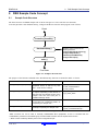
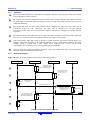
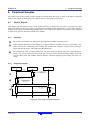
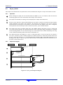
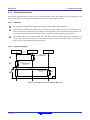
32
RX210 Group
Renesas Starter Kit Software Manual
RENESAS MCU
RX Family / RX200 Series
All information contained in these materials, including products and product specifications,
represents information on the product at the time of publication and is subject to change by
Renesas Electronics Corporation without notice. Please review the latest information published
by Renesas Electronics Corporation through various means, including the Renesas Electronics
Corporation website (http://www.renesas.com).
Rev. 2.00 Jul 2012
Notice
1.
2.
3.
4.
5.
6.
7.
All information included in this document is current as of the date this document is issued. Such information, however, is
subject to change without any prior notice. Before purchasing or using any Renesas Electronics products listed herein, please
confirm the latest product information with a Renesas Electronics sales office. Also, please pay regular and careful attention to
additional and different information to be disclosed by Renesas Electronics such as that disclosed through our website.
Renesas Electronics does not assume any liability for infringement of patents, copyrights, or other intellectual property rights
of third parties by or arising from the use of Renesas Electronics products or technical information described in this document.
No license, express, implied or otherwise, is granted hereby under any patents, copyrights or other intellectual property rights
of Renesas Electronics or others.
You should not alter, modify, copy, or otherwise misappropriate any Renesas Electronics product, whether in whole or in part.
Descriptions of circuits, software and other related information in this document are provided only to illustrate the operation of
semiconductor products and application examples. You are fully responsible for the incorporation of these circuits, software,
and information in the design of your equipment. Renesas Electronics assumes no responsibility for any losses incurred by
you or third parties arising from the use of these circuits, software, or information.
When exporting the products or technology described in this document, you should comply with the applicable export control
laws and regulations and follow the procedures required by such laws and regulations. You should not use Renesas
Electronics products or the technology described in this document for any purpose relating to military applications or use by
the military, including but not limited to the development of weapons of mass destruction. Renesas Electronics products and
technology may not be used for or incorporated into any products or systems whose manufacture, use, or sale is prohibited
under any applicable domestic or foreign laws or regulations.
Renesas Electronics has used reasonable care in preparing the information included in this document, but Renesas Electronics
does not warrant that such information is error free. Renesas Electronics assumes no liability whatsoever for any damages
incurred by you resulting from errors in or omissions from the information included herein.
Renesas Electronics products are classified according to the following three quality grades: “Standard”, “High Quality”, and
“Specific”. The recommended applications for each Renesas Electronics product depends on the product’s quality grade, as
indicated below. You must check the quality grade of each Renesas Electronics product before using it in a particular
application. You may not use any Renesas Electronics product for any application categorized as “Specific” without the prior
written consent of Renesas Electronics. Further, you may not use any Renesas Electronics product for any application for
which it is not intended without the prior written consent of Renesas Electronics. Renesas Electronics shall not be in any way
liable for any damages or losses incurred by you or third parties arising from the use of any Renesas Electronics product for an
application categorized as “Specific” or for which the product is not intended where you have failed to obtain the prior written
consent of Renesas Electronics. The quality grade of each Renesas Electronics product is “Standard” unless otherwise
expressly specified in a Renesas Electronics data sheets or data books, etc.
“Standard”:
Computers; office equipment; communications equipment; test and measurement equipment; audio and visual
equipment; home electronic appliances; machine tools; personal electronic equipment; and industrial robots.
“High Quality”: Transportation equipment (automobiles, trains, ships, etc.); traffic control systems; anti-disaster systems; anticrime systems; safety equipment; and medical equipment not specifically designed for life support.
“Specific”:
Aircraft; aerospace equipment; submersible repeaters; nuclear reactor control systems; medical equipment or
systems for life support (e.g. artificial life support devices or systems), surgical implantations, or healthcare
intervention (e.g. excision, etc.), and any other applications or purposes that pose a direct threat to human life.
8.
You should use the Renesas Electronics products described in this document within the range specified by Renesas Electronics,
especially with respect to the maximum rating, operating supply voltage range, movement power voltage range, heat radiation
characteristics, installation and other product characteristics. Renesas Electronics shall have no liability for malfunctions or
damages arising out of the use of Renesas Electronics products beyond such specified ranges.
9.
Although Renesas Electronics endeavors to improve the quality and reliability of its products, semiconductor products have
specific characteristics such as the occurrence of failure at a certain rate and malfunctions under certain use conditions. Further,
Renesas Electronics products are not subject to radiation resistance design. Please be sure to implement safety measures to
guard them against the possibility of physical injury, and injury or damage caused by fire in the event of the failure of a
Renesas Electronics product, such as safety design for hardware and software including but not limited to redundancy, fire
control and malfunction prevention, appropriate treatment for aging degradation or any other appropriate measures. Because
the evaluation of microcomputer software alone is very difficult, please evaluate the safety of the final products or system
manufactured by you.
10. Please contact a Renesas Electronics sales office for details as to environmental matters such as the environmental
compatibility of each Renesas Electronics product. Please use Renesas Electronics products in compliance with all applicable
laws and regulations that regulate the inclusion or use of controlled substances, including without limitation, the EU RoHS
Directive. Renesas Electronics assumes no liability for damages or losses occurring as a result of your noncompliance with
applicable laws and regulations.
11. This document may not be reproduced or duplicated, in any form, in whole or in part, without prior written consent of Renesas
Electronics.
12.
Please contact a Renesas Electronics sales office if you have any questions regarding the information contained in this
document or Renesas Electronics products, or if you have any other inquiries.
(Note 1) “Renesas Electronics” as used in this document means Renesas Electronics Corporation and also includes its majorityowned subsidiaries.
(Note 2) “Renesas Electronics product(s)” means any product developed or manufactured by or for Renesas Electronics.
Disclaimer
By using this Renesas Starter Kit (RSK), the user accepts the following terms:
The RSK is not guaranteed to be error free, and the entire risk as to the results and performance of the RSK is
assumed by the User. The RSK is provided by Renesas on an “as is” basis without warranty of any kind whether
express or implied, including but not limited to the implied warranties of satisfactory quality, fitness for a particular
purpose, title and non-infringement of intellectual property rights with regard to the RSK. Renesas expressly
disclaims all such warranties. Renesas or its affiliates shall in no event be liable for any loss of profit, loss of data,
loss of contract, loss of business, damage to reputation or goodwill, any economic loss, any reprogramming or recall
costs (whether the foregoing losses are direct or indirect) nor shall Renesas or its affiliates be liable for any other
direct or indirect special, incidental or consequential damages arising out of or in relation to the use of this RSK, even
if Renesas or its affiliates have been advised of the possibility of such damages.
Precautions
The following precautions should be observed when operating any RSK product:
This Renesas Starter Kit is only intended for use in a laboratory environment under ambient temperature and humidity
conditions. A safe separation distance should be used between this and any sensitive equipment. Its use outside the
laboratory, classroom, study area or similar such area invalidates conformity with the protection requirements of the
Electromagnetic Compatibility Directive and could lead to prosecution.
The product generates, uses, and can radiate radio frequency energy and may cause harmful interference to radio
communications. However, there is no guarantee that interference will not occur in a particular installation. If this
equipment causes harmful interference to radio or television reception, which can be determined by turning the
equipment off or on, you are encouraged to try to correct the interference by one or more of the following measures;
·
ensure attached cables do not lie across the equipment
·
reorient the receiving antenna
·
increase the distance between the equipment and the receiver
·
connect the equipment into an outlet on a circuit different from that which the receiver is connected
·
power down the equipment when not is use
·
consult the dealer or an experienced radio/TV technician for help NOTE: It is recommended that wherever
possible shielded interface cables are used.
The product is potentially susceptible to certain EMC phenomena. To mitigate against them it is recommended that the
following measures be undertaken;
·
The user is advised that mobile phones should not be used within 10m of the product when in use.
·
The user is advised to take ESD precautions when handling the equipment.
The Renesas Starter Kit does not represent an ideal reference design for an end product and does not fulfil the
regulatory standards for an end product.
How to Use This Manual
1.
Purpose and Target Readers
This manual is designed to provide the user with an understanding of the RSK hardware functionality, and electrical
characteristics. It is intended for users designing sample code on the RSK platform, using the many different
incorporated peripheral devices.
The manual comprises of an overview of the capabilities of the RSK product, but does not intend to be a guide to
embedded programming or hardware design. Further details regarding setting up the RSK and development
environment can found in the tutorial manual.
Particular attention should be paid to the precautionary notes when using the manual. These notes occur within the body
of the text, at the end of each section, and in the Usage Notes section.
The revision history summarizes the locations of revisions and additions. It does not list all revisions. Refer to the text of
the manual for details.
The following documents apply to the RX210 Group. Make sure to refer to the latest versions of these documents.
The newest versions of the documents listed may be obtained from the Renesas Electronics Web site.
Document Type
Description
Document Title
Document No.
User’s Manual
Describes the technical details of the RSK hardware.
RSK RX210 User
Manual
R20UT0302EG
Software Manual
Describes the functionality of the sample code, and
its interaction with the Renesas Peripheral Driver
Library (RPDL)
RSK RX210
Software Manual
R20UT0305EG
Tutorial
Provides a guide to setting up RSK environment,
running sample code and debugging programs.
RSK RX210
Tutorial Manual
R20UT0303EG
Quick Start Guide
Provides simple instructions to setup the RSK and
run the first sample, on a single A4 sheet.
RSK RX210 Quick
Start Guide
R20UT0304EG
Schematics
Full detail circuit schematics of the RSK.
RSK RX210
Schematics
R20UT0301EG
Hardware Manual
Provides technical
microcontroller.
RX210 Hardware
Manual
R01UH0037EJ
details
of
the
RX210
2.
List of Abbreviations and Acronyms
Abbreviation
Full Form
CPU
DOC
Central Processing Unit
Data Operation Circuit
ELC
MCU
Event Link Controller
Microcontroller Unit
SCI
SPI
Serial Communication Interface
Serial Peripheral Interface
PWM
DMAC
Pulse Width Modulation
Direct Memory Access Controller
WDT
RTC
Watchdog Timer
Real Time Clock
DTC
IIC
Data Transfer Controller
Phillips™ Inter-Integrated Circuit Connection Bus
CRC
Cyclic Redundancy Check
Table of Contents
1. Overview ............................................................................................................................................ 8
1.1
1.2
Purpose...................................................................................................................................................................... 8
Note Regarding Document........................................................................................................................................ 8
2. RSK Sample Code Concept ............................................................................................................... 9
2.1
Sample Code Structure.............................................................................................................................................. 9
3. Tutorial Samples .............................................................................................................................. 10
3.1
Tutorial .................................................................................................................................................................... 10
3.1.1
Description ................................................................................................................................................... 10
3.1.2
Operation .......................................................................................................................................................11
3.1.3
Sequence Diagram.........................................................................................................................................11
3.1.4
RPDL Integration ......................................................................................................................................... 12
3.2
Application.............................................................................................................................................................. 13
3.2.1
Description ................................................................................................................................................... 13
4. Peripheral Samples........................................................................................................................... 14
4.1
ADC12_Repeat ....................................................................................................................................................... 14
4.1.1
Operation ...................................................................................................................................................... 14
4.1.2
Sequence Diagram........................................................................................................................................ 14
4.1.3
RPDL Integration ......................................................................................................................................... 15
4.2
Async_Serial ........................................................................................................................................................... 16
4.2.1
Operation ...................................................................................................................................................... 16
4.2.2
Sequence Diagram........................................................................................................................................ 16
4.2.3
RPDL Integration ......................................................................................................................................... 17
4.3
CRC ........................................................................................................................................................................ 18
4.3.1
Description ................................................................................................................................................... 18
4.3.2
Operation ...................................................................................................................................................... 18
4.3.3
Sequence Diagram........................................................................................................................................ 18
4.3.4
RPDL Integration ......................................................................................................................................... 19
4.4
DMAC .................................................................................................................................................................... 20
4.4.1
Operation ...................................................................................................................................................... 20
4.4.2
Sequence Diagram........................................................................................................................................ 20
4.4.3
RPDL Integration ......................................................................................................................................... 20
4.5
DTC ........................................................................................................................................................................ 21
4.5.1
Operation ...................................................................................................................................................... 21
4.5.2
Sequence Diagram........................................................................................................................................ 21
4.5.3
RPDL Integration ......................................................................................................................................... 22
4.6
LVD......................................................................................................................................................................... 23
4.6.1
Description ................................................................................................................................................... 23
4.6.2
Operation ...................................................................................................................................................... 23
4.6.3
Sequence Diagram........................................................................................................................................ 23
4.6.4
RPDL Integration ......................................................................................................................................... 24
4.7
Power_Down........................................................................................................................................................... 25
4.7.1
Operation ...................................................................................................................................................... 25
4.7.2
Sequence Diagram........................................................................................................................................ 25
4.7.3
RPDL Integration ......................................................................................................................................... 26
4.8
Timer_Mode............................................................................................................................................................ 27
4.8.1
Operation ...................................................................................................................................................... 27
4.8.2
Sequence Diagram........................................................................................................................................ 27
4.8.3
RPDL Integration ......................................................................................................................................... 27
4.9
PWM ....................................................................................................................................................................... 28
4.9.1
Operation ...................................................................................................................................................... 28
4.9.2
Sequence Diagram........................................................................................................................................ 28
4.9.3
RPDL Integration ......................................................................................................................................... 29
4.10 WDT ....................................................................................................................................................................... 30
4.10.1
Operation ...................................................................................................................................................... 30
4.10.2
Sequence Diagram........................................................................................................................................ 30
4.10.3
RPDL Integration ......................................................................................................................................... 31
4.11 RTC ......................................................................................................................................................................... 32
4.11.1
Operation ...................................................................................................................................................... 32
4.11.2
Sequence Diagram........................................................................................................................................ 32
4.11.3
RPDL Integration ......................................................................................................................................... 33
4.12 IIC_Master .............................................................................................................................................................. 34
4.12.1
Operation ...................................................................................................................................................... 34
4.12.2
Sequence Diagram........................................................................................................................................ 34
4.12.3
RPDL Integration ......................................................................................................................................... 35
4.13 SPI_Loopback ......................................................................................................................................................... 36
4.13.1
Operation ...................................................................................................................................................... 36
4.13.2
Sequence Diagram........................................................................................................................................ 36
4.13.3
RPDL Integration ......................................................................................................................................... 37
4.14 Temperature Sensor................................................................................................................................................. 38
4.14.1
Operation ...................................................................................................................................................... 38
4.14.2
Sequence Diagram........................................................................................................................................ 38
4.14.3
RPDL Integration ......................................................................................................................................... 39
4.15 Analog_Compare .................................................................................................................................................... 40
4.15.1
Operation ...................................................................................................................................................... 40
4.15.2
Sequence Diagram........................................................................................................................................ 40
4.15.3
RPDL Integration ......................................................................................................................................... 41
4.16 Data Operation Circuit (DOC) ................................................................................................................................ 42
4.16.1
Operation ...................................................................................................................................................... 42
4.16.2
Sequence Diagram........................................................................................................................................ 42
4.16.3
RPDL Integration ......................................................................................................................................... 43
4.17 Event Link Controller (ELC) .................................................................................................................................. 44
4.17.1
Operation ...................................................................................................................................................... 44
4.17.2
Sequence Diagram........................................................................................................................................ 44
4.17.3
RPDL Integration ......................................................................................................................................... 45
4.18 Low_Power ............................................................................................................................................................. 46
4.18.1
Operation ...................................................................................................................................................... 46
4.18.2
Sequence Diagram........................................................................................................................................ 46
4.18.3
RPDL Integration ......................................................................................................................................... 47
5. Additional Information..................................................................................................................... 48
RSK RX210
RENESAS STARTER KIT
R20UT0305EG0200
Rev 2.00
Jul. 09, 2012
1. Overview
1.1
Purpose
RSK is an evaluation tool for Renesas microcontrollers. This manual explains the operation of the sample code
provided, and its interaction with the Renesas Peripheral Driver Library (RPDL). The Renesas Peripheral Driver
Library (hereinafter “this library” or RPDL) is based upon a unified API (Application Programming Interface) for
the microcontrollers made by Renesas Electronics Corporation.
This manual is not intended to be a tutorial on using RPDL, or how RPDL works – it simply aims to explain to the
reader how the RPDL was used to create the sample code supplied with the RSK. For further information regarding
RPDL, refer to the RPDL API User’s Manual supplied with the RSK. Alternatively, visit the PDG (Peripheral Driver
Group) section of the Renesas website:
http://www.renesas.com/pdg
1.2
Note Regarding Document
This document explains by text and diagrams the functionality of the sample code and its interaction with the
Renesas Peripheral Driver Library (RPDL). The RPDL is preliminary and functionally tested to operate with the
RSKRX210 sample code only.
This manual aims to be as clear as possible, by matching the reference sample code as closely as possible. There
may be some cases however where the function names in the code differ slightly this document. This does not
change its functionality as described in this manual.
R20UT0305EG0200 Rev.2.00
Jul 09, 2012
Page 8 of 52
RSKRX210
2. RSK Sample Code Concept
2. RSK Sample Code Concept
2.1
Sample Code Structure
The basic structure of all RSK sample code is shown in Figure 2-1 below. The first two functions,
‘PowerOn_ResetPC’ and ‘HardwareSetup’, configure the MCU before the main program code executes.
Reset
PowerOn_ResetPC( )
HardwareSetup( )
Hardware setup consists of the
following functions:
ConfigureOperatingFrequency( )
ConfigureOutputPorts( )
EnablePeripheralModules( )
ConfigureInterrupts( )
main( )
Final State
Figure 2-1: Sample Code Structure
The purpose of the functions included in the ‘HardwareSetup’ function are detailed in Table 2-1 below.
Function Name
Purpose
ConfigureOperatingFrequency
Initialises the main MCU, bus and
peripheral clocks; as well as any realtime clocks and PLL settings.
R_CGC_Set
Configures the MCU port pins as inputs
or outputs, depending on the devices on
the RSK and the intended function of the
sample code. Also sets some pins to
suitable initial logic levels.
R_IO_PORT_Set
EnablePeripheralModules
Enables or disables peripheral modules
on the MCU not controlled by RPDL, as
required by the sample code.
Non-RPDL functions only*
ConfigureInterrupts
Configures interrupts external hardware
interrupts required by the sample code.
R_INTC_CreateExtInterrupt**
ConfigureOutputPorts
RPDL Functions Used
R_CMT_CreateOneShot
R_CGC_Control
R_IO_PORT_Write
R_INTC_CreateFastInterrupt**
Table 2-1: Hardware Setup Functions
*RPDL functions can not be used to manually enable/disable MCU peripherals, as this is controlled with the
Create/Destroy functions for each RPDL group; therefore RPDL functions are not required in this section.
** RPDL functions indirectly called by the function ConfigureInterrupts.
R20UT0305EG0200 Rev.2.00
Jul 09, 2012
Page 9 of 52
RSKRX210
3. Tutorial Samples
3. Tutorial Samples
3.1
Tutorial
The sample code in this section is basic tutorial code, used to demonstrate basic usage of the RSK and help the user
to begin writing his/her own basic sample code.
3.1.1
Description
The tutorial sample code demonstrates basic usage of the debugger and RSK hardware, and is common to all RSKs.
This sample is supplied programmed onto the MCU, and executes out of the box when power is applied.
The sample calls three main functions to demonstrate port pin control, interrupt usage and C variable initialisation.
These functions are shown in Figure 3-1 below.
main( )
Flash_LED( )
Timer_ADC( )
Static_Test( )
while(1)
Figure 3-1: Tutorial Sample Flow
R20UT0305EG0200 Rev.2.00
Jul 09, 2012
Page 10 of 52
RSKRX210
3.1.2
3. Tutorial Samples
Operation
1
The tutorial code initialises the LCD module, and displays ‘Renesas’ on the first line of the LCD, and the
name of the MCU on the second line.
2
The tutorial code calls the Flash_LED function which creates a timer interrupt, with callback function
CB_TimerLED, to toggle the LEDs repeatedly and waits in a loop until either a switch is pressed or the
LEDs flash 200 times.
3
The tutorial then calls the Timer_ADC function which configures the ADC unit, and a timer unit to
periodically trigger an ADC conversion. The ADC unit is configured to call the function
CB_ADConversion, after each AD conversion completes. The timer is configured to call the function
CB_Timer.
4
The callback function CB_ADConversion is triggered by ADC interrupts. It fetches the ADC result, and
uses it to set a new timer period. The callback function also toggles the user LEDs.
5
After calling Timer_ADC and setting up the timer & ADC interrupts, the tutorial calls the Static_Test
function which runs in parallel to the callback functions in step 4. This function displays the string
‘STATIC’ which is fetched from a static variable and is replaced, letter by letter, by the string
‘TESTTEST’. The LCD then reverts to the original display on completion.
6
After the Static_Test function completes, the MCU waits in an infinite while loop; and is periodically
interrupted with the callback function in step 4.
3.1.3
Sequence Diagram
Figure 3-2 below shows the program execution flow of the tutorial sample.
Main()
LCD
Potentiometer
LED’s
Init_LCD( )
Display_LCD( )
1
<< Displays the sample
name/instructions on the
debug LCD display >>
<< Wait in function and flash
LEDs 200 times or until
switch is pressed >>
Flash_LED( )
2
3
<< Initialise ADC and timer
modules for interrupt
callbacks >>
Timer_ADC( )
<< AD conversion interrupt >>
<< Callback function fetches
ADC result, sets new timer
period based on result, and
flashes the LEDs. >>
4
CB_ADConversion( )
LOOP
5
<< Display the static variable
‘STATIC’ on the LCD and replace
with the string “TESTTEST” >>
Static_Test( )
<< Infinite while loop >>
6
while(1)
Figure 3-2: Tutorial Sequence Diagram
R20UT0305EG0200 Rev.2.00
Jul 09, 2012
Page 11 of 52
RSKRX210
3.1.4
3. Tutorial Samples
RPDL Integration
Table 3-1 below details the RPDL functions used in each sample code function shown in the sequence diagram.
Function
Flash_LED
RPDL Function
R_CMT_Create
R_CMT_Destroy
Start_Timer
R_CMT_Create
Start_ADC
R_ADC_12_Set
R_ADC_12_CreateUnit
R_ADC_12_CreateChannel
R_ADC_12_Control
CB_ADConversion
R_ADC_12_Read
R_CMT_Control
Table 3-1: Tutorial Sample RPDL Integration
R20UT0305EG0200 Rev.2.00
Jul 09, 2012
Page 12 of 52
RSKRX210
3.2
Application
3.2.1
Description
3. Tutorial Samples
The application sample is intended as a starting platform for the user to write his/her own code. The sample
includes all the necessary initialisation code and configuration settings from previous samples. The main( ) function
contains no sample code, and performs no additional functionality.
For more information regarding the hardware initialisation performed before the main( ) function starts, refer back
to §2.
R20UT0305EG0200 Rev.2.00
Jul 09, 2012
Page 13 of 52
RSKRX210
4. Peripheral Samples
4. Peripheral Samples
The sample code in this section provides examples of initialisation and usage of some of the MCU’s peripheral
modules. The sample code also provides examples of how to debug MCU peripherals.
4.1
ADC12_Repeat
This sample code demonstrates usage of the on-chip analogue to digital converter (ADC), in group scan repeat
mode. The sample configures the ADC to repeatedly take readings of the potentiometer voltage (RV1) and other
analogue input signals (available through RSK headers). The sample then updates the conversion value displayed
on the LCD, by periodic interrupts from the timer module.
4.1.1
Operation
1
The sample first initialises the debug LCD, and displays the sample name/instructions.
2
It then calls the function Init_ADC12Repeat, to initialise the ADC module to operate in repeat mode – the
ADC unit will now continuously take readings. The function also initialises an interval timer interrupt,
which calls the CB_Timer_ADC12Repeat callback function.
3
The sample then enters an infinite while loop. The timer interrupt function CB_Timer_ADC12Repeat is
called every interval, and fetches the current AD conversion result. The function then displays the result
onto the debug LCD. The callback function displays a different analogue input reading each time it is
called.
4.1.2
Sequence Diagram
Main()
LCD
Potentiometer
Init_LCD( )
Display_LCD( )
1
<< Displays the sample
name/instructions on the
debug LCD. >>
Init_ADC12Repeat( )
2
<< Configures the ADC unit,
and initialises an interval
timer interrupt. >>
<< Timer interrupt >>
3
while(1)
<< Infinite while loop >>
<< Fetches ADC value, and
displays result on debug
LCD. >>
CB_Timer_
ADC12Repeat( )
LOOP
Figure 4-1: ADC_Repeat Sequence Diagram
R20UT0305EG0200 Rev.2.00
Jul 09, 2012
Page 14 of 52
RSKRX210
4.1.3
4. Peripheral Samples
RPDL Integration
Function
Init_ADC12Repeat
RPDL Function
R_ADC_12_Set
R_ADC_12_CreateUnit
R_ADC_12_CreateChannel
R_CMT_Create
R_ADC_12_Control
CB_Timer_ADC12Repeat
R_ADC_12_Read
Table 4-1: ADC_Repeat Sample RPDL Integration
R20UT0305EG0200 Rev.2.00
Jul 09, 2012
Page 15 of 52
RSKRX210
4.2
4. Peripheral Samples
Async_Serial
This sample code demonstrates an asynchronous serial communication using the on-chip serial interface module.
4.2.1
Operation
Before starting the sample, the user should connect the RSK to a PC via an RS-232 cable and start the
terminal program (refer to the instructions in the sample code comments).
1
The sample first initialises the debug LCD, and displays the sample name/instructions.
2
The Init_Async function is called, which initialises the SCI unit to operate in asynchronous mode with the
settings detailed in the sample code comments. The function also configures a SCI receive interrupt,
which generates an interrupt every time data is received in the SCI unit. Finally a timer unit is configured,
which generates interval interrupts, used to call the CB_Timer_Async callback function.
3
The sample then enters an infinite while loop. The callback function CB_Timer_Async is called with
every timer interval interrupt. The function checks the status of the gSCI_Flag, and continues to transmit
an incrementing number over SCI with the flag is true. The function exits without transmitting if the flag
is false. Whilst transmitting, LED0 will remain on and LED1 off.
4
The callback function CB_SCIReceive_Async is called when data is received on the SCI unit. When a
user enters a character in the terminal program, the callback function is called. The function fetches the
keypress, and if the character is a ‘z’ it sets the gSCI_Flag variable to false. On all other keypresses, it sets
the flag to true. Once ‘z’ has been pressed, LED1 will turn on and LED0 remain off until another key is
pressed to resume transmission.
4.2.2
Sequence Diagram
Main()
LCD
Init_LCD( )
SCI
<< Displays sample name/
instructions on the debug
LCD. >>
Display_LCD( )
1
Init_Async( )
2
<< Initialises the SCI unit
in asynchronous mode,
and also configures a
timer to generate interval
interrupts >>
<< Timer interrupt generated >>
<< Timer callback function
transmits incrementing
numbers via SCI if
gSCI_Flag is true.>>
CB_Timer_Async( )
while(1)
3
LOOP
<< SCI data receive interrupt generated >>
4
CB_SCIReceive_
Async( )
<< Receive function fetches
the received character, and
sets the gSCI_Flag variable
to false if its ‘z’ >>
Figure 4-2: Async_Serial Sequence Diagram
R20UT0305EG0200 Rev.2.00
Jul 09, 2012
Page 16 of 52
RSKRX210
4.2.3
4. Peripheral Samples
RPDL Integration
Function
Init_Async
RPDL Function
R_SCI_Create
R_SCI_Receive
R_SCI_Send
R_CMT_Create
Transmit_Async
R_SCI_Send
R_IO_PORT_Write
CB_Timer_Async
R_SCI_GetStatus
CB_SCIReceive_Async
R_IO_PORT_Write
R_SCI_Receive
Table 4-2: Async_Serial Sample RPDL Integration
R20UT0305EG0200 Rev.2.00
Jul 09, 2012
Page 17 of 52
RSKRX210
4. Peripheral Samples
4.3
CRC
4.3.1
Description
This sample demonstrates the CRC unit, by echoing typed characters from the SCI terminal with a corresponding
checksum.
4.3.2
Operation
Before starting this sample, the user should connect the RSK to the PC via an RS232 serial cable and run a
suitable terminal program (see instructions in sample code comments).
1
The sample first initialises the debug LCD, and displays the sample name/instructions.
2
The sample then calls the function Init_CRC, which configures the CRC unit to produce checksums, and
the SCI unit for asynchronous operation to and from the PC terminal.
3
The sample then enters an infinite while loop, and the rest of the sample’s functionality is performed in
interrupts. When the user presses a key in the terminal, the SCI interrupt executes the callback function
CB_SCIReceive_CRC. This function takes the received character and calls the function Calculate_CRC to
generate a checksum.
4
The function Calculate_CRC inserts the received character into the CRC registers, and fetches the
calculated checksum, and returns it to the CB_SCIReceive_CRC function.
The sample returns from the Calculate_CRC function to the callback function and writes a string
containing the received character and its checksum to the terminal. The sample then returns to the infinite
while loop and waits until a key is entered into the terminal again.
5
4.3.3
Sequence Diagram
Main()
CRC
SCI
LCD
Init_LCD( )
<< Display instructions on
the debug LCD >>
DisplayLCD( )
1
Init_CRC( )
2
<< Initialise the CRC and the
SCI modules. Instructions
are sent to the terminal >>
CB_SCIReceive_CRC( )
while(1)
<< Infinite while loop >>
4
<< SCI receive callback func
-tion generates CRC checksum
of the received character and
displays it on the terminal >>
<< SCI data receive interrupt generated >>
3
<< Function generates CRC
checksum from input value >>
5
Calculate_CRC( )
LOOP
Figure 4-3: CRC Sequence Diagram
R20UT0305EG0200 Rev.2.00
Jul 09, 2012
Page 18 of 52
RSKRX210
4.3.4
4. Peripheral Samples
RPDL Integration
Function
Init_CRC
RPDL Function
R_CRC_Create
R_SCI_Create
R_SCI_Receive
R_SCI_Send
CB_SCIReceive_CRC
R_SCI_GetStatus
R_SCI_Send
R_SCI_Receive
Calculate_CRC
R_CRC_Write
R_CRC_Read
Table 4-3: CRC Sample RPDL Integration
R20UT0305EG0200 Rev.2.00
Jul 09, 2012
Page 19 of 52
RSKRX210
4.4
4. Peripheral Samples
DMAC
This sample code configures the DMAC unit to perform a data transfer to the global variable, gDMA_DataBuff.
4.4.1
Operation
1
The sample initialises the debug LCD and displays instructions on the screen.
2
The function Init_DMAC is called to configure a DMAC channel for consecutive data transfers. The
transfer mode is set to automatically increment the data destination address after each transfer. A callback
function CB_DMACTransferEnd_DMAC is configured to be called on completion of all transfers The
DMAC is enabled and the transfer operation is started before the sample enters an infinite while loop.
On completion of all data transfers, the CB_DMACTransferEnd_DMAC callback function is called and
turns on LED1 to indicate the operation has ended.
3
4.4.2
Sequence Diagram
DMAC
LCD
Main()
Init_LCD( )
<< Displays instructions on
the debug LCD >>
Display_LCD( )
1
<< Configures a DMAC channel
then starts the transfer >>
Init_DMAC( )
2
3
while(1)
<< DMAC interrupt >>
<< Turns on LED1 to indicate
completion of data transfers >>
CB_DMACTransfer
End_DMAC( )
LOOP
Figure 4-4: DMAC Sequence Diagram
4.4.3
RPDL Integration
Function
Init_DMAC
RPDL Function
R_DMAC_Create
R_DMAC_Control
R_INTC_Modify
CB_DMACTransferEnd_DMAC
R_DMAC_GetStatus
R_IO_PORT_Write
R_DMAC_Control
Table 4-4: DMAC Sample RPDL Integration
R20UT0305EG0200 Rev.2.00
Jul 09, 2012
Page 20 of 52
RSKRX210
4.5
4. Peripheral Samples
DTC
This sample demonstrates usage of the DTC unit, by performing a DTC transfer of an ADC result to an
incrementing location in an array when a switch is pressed.
4.5.1
Operation
1
The sample initialises the debug LCD, and displays instructions on the screen.
2
The sample calls the function Init_DTC, which configures the DTC unit and also configures an ADC
channel which will trigger a DTC transfer after a successful conversion. The DTC transfer is configured to
transfer the content of the ADC result register to incrementing locations in the global array,
gDTC_Destination.
The sample then enters an infinite while loop, with the rest of the sample’s functionality completed in
interrupts. When switch SW3 is pressed, the callback function CB_Switch_DTC is called. The callback
function checks the number of remaining transfers, and triggers an AD conversion. If there are no more
remaining transfers, the function clears the contents of the gDTC_Destination array and reconfigures the
DTC transfer to start from the beginning.
3
4.5.2
Sequence Diagram
Main()
LCD
DTC
Init_LCD( )
Display_LCD( )
1
<< Instructions are displayed
on the debug LCD >>
<< Configures the DTC unit
for a normal transfer >>
Init_DTC( )
2
<< Switch interrupt >>
3
while(1)
<< Infinite while loop >>
<< Switch callback function
triggers AD conversion,
which then triggers a DTC
transfer. >>
CB_Switch_
DTC( )
LOOP
Figure 4-5: DTC Sequence Diagram
R20UT0305EG0200 Rev.2.00
Jul 09, 2012
Page 21 of 52
RSKRX210
4.5.3
4. Peripheral Samples
RPDL Integration
Function
Init_DTC
RPDL Function
R_DTC_Set
R_DTC_Create
R_DTC_Control
R_ADC_12_Set
R_ADC_12_CreateUnit
R_ADC_12_CreateChannel
R_INTC_Write
R_INTC_Modify
CB_Switch_DTC
R_DTC_GetStatus
R_DTC_Control
R_INTC_Write
R_ADC_12_Control
R_IO_PORT_Modify
Table 4-5: DTC Sample RPDL Integration
R20UT0305EG0200 Rev.2.00
Jul 09, 2012
Page 22 of 52
RSKRX210
4. Peripheral Samples
4.6
LVD
4.6.1
Description
In this sample, the LVD (Low Voltage Detection) circuit’s is configured to generate an interrupt when the power
supply equals or falls below the detection level.
4.6.2
Operation
Before starting this sample, follow the instructions in main source file to ensure the RSK is configured
correctly. Connect a 5V variable power supply to the power socket, and set the initial voltage to 5V.
1
The sample initialises the debug LCD, and displays instructions on the screen.
2
The sample then calls the Init_VDET function, which initialises the LVD unit to generate interrupts when
VCC drops to 4.0V and 1.9V. The function also configures a CMT timer, to periodically toggle the user
LEDs.
The sample then enters an infinite while loop. The while loop periodically interrupt by the callback
function CB_Timer_VDET. If the global gLEDsync_flg is set, it toggles LEDs LED0 to LED2
synchronously, and LED3 asynchronously. If gLEDsync_flg is not set, it toggles all the user LEDs
together.
When the input voltage is lowered to below 4.0V, the CB_LVD2_VDET callback function is called by the
voltage detect interrupt. This function sets the gLEDsync_flg, turns off LEDs LED0 to LED2, and waits
until the supply voltage returns to over 4.0V.
When the input voltage is lowered to below 1.9V, the CB_NMI_VDET callback function is called by the
non-maskable voltage detect interrupt. This interrupts any other callback functions that may be running.
This function turns off all the user LEDs, and waits until the voltage level rises above 1.9V before exiting.
3
4
5
4.6.3
Sequence Diagram
Main()
LCD
CMT
LVD
Init_LCD( )
Display_LCD( )
1
Init_VDET( )
2
<< Displays the sample
name/instructions on the
debug LCD. >>
<< Initialises LVD circuit,
NMI interrupt and a timer
for updating the LCD. >>
<< Timer interrupt >>
<< Toggles the user LEDs. If
gLEDsync_flg is set, LED3 toggles
asynchronously to the other LEDs.
Otherwise, all LEDs toggle
together. >>
3
CB_Timer_VDET( )
LOOP
<< Voltage detect (4.0V) interrupt >>
<< Callback function triggered
by voltage detect interrupt.
Function sets gLEDsync_flg,
and waits until the voltage
goes above 4.0V again. >>
while(1)
4
CB_LVD2_VDET( )
<< Voltage detect (1.9V) NMI interrupt >>
5
<< Callback function triggered by
voltage detect NMI interrupt. Function
interrupts any callbacks, turns offs
LED3 and waits until the voltage
returns above 1.9V, then turns LED3
back on before exiting. >>
CB_NMI_VDET( )
Figure 4-6: LVD Sequence Diagram
R20UT0305EG0200 Rev.2.00
Jul 09, 2012
Page 23 of 52
RSKRX210
4.6.4
4. Peripheral Samples
RPDL Integration
Function
Init_VDET
RPDL Function
R_LVD_Create
R_INTC_CreateExtInterrupt
R_CMT_Create
CB_Timer_VDET
CB_LVD2_VDET
R_IO_PORT_Modify
R_CMT_Control
R_IO_PORT_Write
R_LVD_GetStatus
R_INTC_Write
CB_NMI_VDET
R_IO_PORT_Write
R_LVD_GetStatus
R_INTC_ControlExtInterrupt
Table 4-6: Low Voltage Detection Sample RPDL Integration
R20UT0305EG0200 Rev.2.00
Jul 09, 2012
Page 24 of 52
RSKRX210
4.7
4. Peripheral Samples
Power_Down
This sample code configures the MCU’s low power consumption’s settings and enters the MCU into standby mode.
The RTC is configured to interrupt and wake the MCU at intervals of 1 second, to update the LCD with the time
elapsed since the program was started.
4.7.1
Operation
1
The sample initialises the debug LCD and displays ‘PWR MODE’ (Power Mode) on the first line of the
LCD, and the current power mode, ‘Active’ on the second line.
2
The sample then calls the function Init_PowerDown which configures the low power consumption and
real time clock registers.
3
The sample then enters an infinite while loop. The while loop immediately enters the MCU into standby
mode. After a second, the RTC unit triggers an interrupt which wakes the MCU from standby mode and
calls the callback function CB_RTC_PowerDown.
4
The function CB_RTC_PowerDown reads the time from the RTC unit, and updates the LCD display with
the current time (time elapsed since program began). The program then returns back to the while loop, and
repeats step 3 & 4 infinitely.
4.7.2
Sequence Diagram
Main()
LCD
RTC
Init_LCD( )
<< Displays the sample
name/instructions on the
debug LCD >>
Display_LCD( )
1
Init_PowerDown( )
<< Configures the real time clock
unit to create an interrupt every
second, and execute the CB_RTC_
PowerDown callback function. >>
2
<<<<<<<<<<<<<<<<<<<< MCU Enters Standby Mode >>>>>>>>>>>>>>>>>>>>
while(1)
3
<< Real time clock interrupt detected >>
4
<< Program returns to
while loop, and enters
standby mode again. >>
<< Real time clock interrupt
occurs, and wakes MCU
from sleep. Function
updates LCD with RTC
time. >>
CB_RTC_PowerDown( )
LOOP
Figure 4-7: Power_Down Sequence Diagram
R20UT0305EG0200 Rev.2.00
Jul 09, 2012
Page 25 of 52
RSKRX210
4.7.3
4. Peripheral Samples
RPDL Integration
Function
Init_PowerDown
RPDL Function
R_RTC_Create
R_RTC_Control
R_LPC_Create
CB_RTC_PowerDown
R_RTC_Read
R_CMT_CreateOneShot
Table 4-7: Power_Down Sample RPDL Integration
R20UT0305EG0200 Rev.2.00
Jul 09, 2012
Page 26 of 52
RSKRX210
4.8
4. Peripheral Samples
Timer_Mode
This sample code configures the timer to generate 1 KHz waveform. The waveform can be seen on the
oscilloscope.
4.8.1
Operation
Before starting this sample, the user should refer to the sample code instructions in order to connect the
oscilloscope to the correct location.
1
The sample initialises the debug LCD and displays the sample name/instructions on the screen.
2
The sample then configures a timer channel to output a 1 KHz periodic square wave with 50% duty.
3
The sample then enters an infinite while loop. The timer unit will continue to produce the waveform.
4.8.2
Sequence Diagram
Main()
LCD
Init_LCD( )
Display_LCD( )
1
<< Displays the sample
name/instructions on the
debug LCD. >>
Init_TimerMode( )
2
<< Configures a timer unit to
produce a 1KHz squarewave
output. >>
while(1)
3
<< Infinite while loop. >>
Figure 4-8: Timer Mode Sequence Diagram
4.8.3
RPDL Integration
Function
Init_TimerMode
RPDL Function
R_MTU2_Set
R_MTU2_Create
R_MTU2_ControlChannel
CB_Timer_TimerMode
R_IO_PORT_Modiy
Table 4-8: Timer Mode Sample RPDL Integration
R20UT0305EG0200 Rev.2.00
Jul 09, 2012
Page 27 of 52
RSKRX210
4.9
4. Peripheral Samples
PWM
This sample code configures the timer to generate a 1KHz waveform, with a constantly changing duty cycle. The
duty cycle begins at 10% and gradually increases to 90%, then cycles back to 10% continuously until the user
presses switch 1 and freezes the duty cycle. The value at this freeze-point is displayed on the debug LCD.
4.9.1
Operation
Before starting this sample, the user should refer to the sample code instructions in order to connect the
oscilloscope to the correct location.
1
The sample initialises the debug LCD and displays the sample name/instructions on the screen.
2
It then calls the function Init_PWM which configures a timer channel to generate an initial periodic 1 KHz
output signal with a 10% duty cycle. The function configures the timer to generate an interrupt at the end
of each period, serviced by the callback function CB_Timer_PWM. The function also configures a switch
interrupt and callback function.
3
The CB_Timer_PWM callback function increments the duty cycle each time it is executed if the duty
cycle is less than 90%, otherwise it resets the duty cycle to 10%.
When the user switch is pressed, the callback function CB_Switch_PWM is called. The function prevents
the duty cycle from changing, and displays the current duty cycle on the debug LCD.
4
4.9.2
Sequence Diagram
Main()
LCD
Timer
Switch
Init_ LCD( )
Display_ LCD( )
1
<< Instructions are displayed on the
debug LCD >>
Init_ PWM( )
2
<< Initialises a timer channel for
compare match operations >>
<< Interval timer interrupt >>
<< Timer callback function
called on timer interrupts to
update the duty cycle. >>
while(1)
3
4
CB_ Timer_ PWM( )
<< Switch interrupt >>
<< The switch callback function stops and
captures the timer count which is then
displayed on the debug LCD as a
percentage. It also prevents further
updates of the timer’s period. >>
CB_ Switch_ PWM( )
LOOP
Figure 4-9: PWM Sequence Diagram
R20UT0305EG0200 Rev.2.00
Jul 09, 2012
Page 28 of 52
RSKRX210
4.9.3
4. Peripheral Samples
RPDL Integration
Function
Init_PWM
RPDL Function
R_TMR_Set
R_TMR_CreatePeriodic
CB_Timer_PWM
R_TMR_ControlPeriodic
Table 4-9: PWM Sample RPDL Integration
R20UT0305EG0200 Rev.2.00
Jul 09, 2012
Page 29 of 52
RSKRX210
4.10
4. Peripheral Samples
WDT
This sample code demonstrates the usage of the watchdog timer functionality; by resetting the WDT count
regularly, at a rate controlled by the potentiometer to prevent its period from timing out. When the WDT’s period is
reached, the LEDs stop flashing and the program halts in an infinite while loop.
4.10.1
Operation
Before starting this sample, ensure that the potentiometer shaft is turned anti-clockwise fully.
1
The sample initialises the debug LCD and displays the sample name/instructions on the screen.
2
The Init_WDT function configures the watchdog timer unit, the ADC unit and a timer unit. The ADC unit
is configured to operate in continuous mode, and the timer is configured to generate an interval interrupt
that executes the callback function CB_Timer_WDT.
3
The sample then enters an infinite while loop. The while loop is interrupted by the CB_Timer_WDT
callback function. This function resets the WDT count, toggles the LEDs and fetches the ADC result. This
result is used to set the new timer interval period. By adjusting the potentiometer, the length between
WDT resets is varied.
4
When the WDT reset interval is too long, the watchdog timer will overflow and trigger an interrupt, which
calls the callback function CB_Overflow_WDT. This function sets the LEDs to static, displays a
watchdog overflow message on the debug LCD and waits in an infinite while loop.
4.10.2
Sequence Diagram
Main()
LCD
ADC
WDT
Init_LCD( )
Display_LCD( )
1
Init_WDT( )
2
<< Displays the sample
name/instructions on the
debug LCD. >>
<< Initialises WDT unit, ADC
unit and an interval timer to
trigger callback function
CB_Timer_WDT. >>
3
while(1)
<< Timer interrupt >>
<< Callback function interval timer.
Function resets the WDT count,
toggles the LEDs, fetches the ADC
result and uses to calculate a new
timer period. >>
CB_Timer_WDT( )
LOOP
<< WDT overflow interrupt >>
4
<< Callback function triggered
by WDT overflow interrupt.
Function displays overflow
message on the debug LCD,
sets the LEDs as steady on,
and waits in an infinite while
loop. >>
CB_Overflow
_WDT( )
Figure 4-10: WDT Sequence Diagram
R20UT0305EG0200 Rev.2.00
Jul 09, 2012
Page 30 of 52
RSKRX210
4.10.3
4. Peripheral Samples
RPDL Integration
Function
Init_WDT
RPDL Function
R_ADC_12_Set
R_ADC_12_CreateUnit
R_ADC_12_CreateChannel
R_ADC_12_Control
R_CMT_Create
R_WDT_Set
R_INTC_CreateExtInterrupt
R_WDT_Control
CB_Timer_WDT
R_WDT_Control
R_ADC_12_Read
R_IO_PORT_Modify
R_CMT_Control
CB_WDTOverflow
R_IO_Port_Write
Table 4-10: WDT Sample RPDL Integration
R20UT0305EG0200 Rev.2.00
Jul 09, 2012
Page 31 of 52
RSKRX210
4.11
4. Peripheral Samples
RTC
This sample code demonstrates the usage of the real time clock’s functionality by running a timer from a
32.768 KHz clock source. The time is displayed on the debug LCD using the 24-hour digital format hh:mm:ss,
starting from 00:00:00.
4.11.1
Operation
1
The sample initialises the debug LCD and displays the sample name/instructions on the screen.
2
The sample then calls the Init_RTC to initialise the RTC settings and configures two callback functions
CB_Alarm_RTC and CB_1HZ_RTC.
3
The sample enters an infinite while loop, which is interrupted every second by the RTC callback function,
CB_1HZ_RTC. This function fetches the time (time elapsed from sample start) from the RTC unit, and
displays it on the debug LCD.
4
The while loop is interrupted again when the time matches the alarm time. The interrupt executes the
callback function CB_Alarm_RTC, which turns on LED1.
4.11.2
Sequence Diagram
Main()
LCD
RTC
Init_LCD( )
Display_LCD( )
1
<< Displays the sample
name/instructions on the
debug LCD. >>
<< Initialises the RTC unit >>
Init_RTC( )
2
<< RTC 1Hz interrupt >>
<< Callback function is trigger
by the RTC 1Hz interrupt.
Function updates the time
from the RTC unit to the
debug LCD. >>
while(1)
3
4
CB_1HZ_RTC( )
LOOP
<< RTC Alarm interrupt >>
<< Callback function is
triggered by the RTC alarm.
Function sets LED1 on. >>
CB_Alarm_RTC( )
Figure 4-11: RTC Sequence Diagram
R20UT0305EG0200 Rev.2.00
Jul 09, 2012
Page 32 of 52
RSKRX210
4.11.3
4. Peripheral Samples
RPDL Integration
Function
Init_RTC
CB_1HZ_RTC
CB_Alarm_RTC
RPDL Function
R_RTC_Create
R_RTC_Control
R_RTC_Read
R_IO_PORT_Write
Table 4-11: RTC Sample RPDL Integration
R20UT0305EG0200 Rev.2.00
Jul 09, 2012
Page 33 of 52
RSKRX210
4.12
4. Peripheral Samples
IIC_Master
This sample demonstrates usage of the IIC unit in master mode, by performing read and write operations to an
EEPROM memory device. The sample is configured to work with the following Renesas devices:
· HN58X24512I, 1Mbit EEPROM, 1MHz
4.12.1
Operation
1
The sample initialises the debug LCD and displays the sample name/instructions on the screen.
2
The sample then enters the main IIC master sequence loop, where it first calls the Init_EEPROM_Master
function which configures the IIC unit to operate in master mode.
3
The master sequence then waits in an infinite while loop, polling the user switch flag. When switch SW2
is pressed, an EEPROM device write operation is executed using the Write_EEPROM_Master function.
The write operation writes the string “XXRenesas IIC ”, where XX is replaced with an ASCII data
identifier, which increments with every write operation. If the write operation fails, the debug LCD
displays “Error W.”
4
When switch SW3 is pressed, an EEPROM device read operation is executed using the
Read_EEPROM_Master function. The first 16 bytes of the EEPROM device’s memory are read. If the
read data matches the expected data string, “XXRenesas IIC ”, the data identifier (XX) is displayed on
the debug LCD to indicate a successful read operation. If the read operation fails, the debug LCD displays
“Error R.”.
4.12.2 Sequence Diagram
Main()
I2C Bus
LCD
Init_LCD( )
<< Instructions are displayed on the debug LCD >>
DisplayLCD( )
1
<< The I2C unit is configured
for master mode >>
Init_EEPROM_Master( )
3
MasterSequence_EEPROM( )
2
<< Switch 2 press interrupt >>
<< Switch 3 press interrupt >>
4
<< A data string is written to
an EEPROM memory
starting from address 0
when switch SW2 is pressed
>>
Write_EERPOM_Master( )
<< The contents of an
EEPROM memory location is
read, and checked against
the output data string >>
Read_EERPOM_Master( )
LOOP
Figure 4-12: IIC_Master Sequence Diagram
R20UT0305EG0200 Rev.2.00
Jul 09, 2012
Page 34 of 52
RSKRX210
4.12.3
4. Peripheral Samples
RPDL Integration
Function
RPDL Function
Init_EEPROM_Master
R_IIC_Set
R_IIC_Create
Write_EEPROM_Master
R_IIC_MasterSend
R_CMT_CreateOneShot
Read_EEPROM_Master
R_IIC_MasterSend
R_IIC_MasterReceive
R_CMT_CreateOneShot
CheckStatus_EEPROM_Master
R_IIC_GetStatus
BusActivity_IIC
R_IO_PORT_Write
Table 4-12: IIC_Master Sample RPDL Integration
R20UT0305EG0200 Rev.2.00
Jul 09, 2012
Page 35 of 52
RSKRX210
4.13
4. Peripheral Samples
SPI_Loopback
This sample code demonstrates usage of the SPI unit by performing a simple loopback test.
4.13.1
Operation
This sample may require hardware modifications in order to operate. Refer to the sample code instructions
for further information before proceeding.
1
The sample first initialises the debug LCD, and displays the sample name/instructions.
2
The Init_SPI function is called, which initialises the SPI unit and configures an SPI receive interrupt
callback. An ADC unit is configured for single scan operations. The function also configures a switch
callback function.
3
The sample then enters an infinite while loop. When the user presses the switch specified (see sample
code comments), the callback function CB_Switch is called. This callback function takes an ADC reading,
and transmits it via the SPI loopback.
4
The data transmitted in the CB_Switch function is received by the loopback SPI, and generates an
interrupt. The SPI receive interrupt calls the CB_SPIReceive callback function, which fetches the received
data and compares it against the original value sent. If they match, it displays the result on the debug
LCD. If there is a mismatch between sent and received data, an error is reported on the debug LCD.
4.13.2
Sequence Diagram
Main()
LCD
SPI
Init_LCD( )
Display_LCD( )
1
2
Init_SPI( )
<< Displays the sample
name/instructions on the
debug LCD display >>
<< Initialise SPI unit, configures
an SPI receive interrupt and
configures a switch interrupt
callback function. >>
<< Switch interrupt >>
<< Infinite while loop >>
<< Callback function takes
ADC reading, and transmits
the result via SPI loopback. >>
3
CB_Switch( )
<< SPI receive interrupt >>
4
<< Callback function reads
data sent via SPI loopback
and compares against original
reading, and displays the
value on the debug LCD. >>
CB_SPIReceive( )
Figure 4-13: SPI Loopback Sequence Diagram
R20UT0305EG0200 Rev.2.00
Jul 09, 2012
Page 36 of 52
RSKRX210
4.13.3
4. Peripheral Samples
RPDL Integration
Function
Init_SPI
RPDL Function
R_SPI_Create
R_SPI_Control
R_SPI_Command
R_ADC_12_Set
R_ADC12_Create_Unit
R_ADC_12_CreateChannel
CB_Switch
R_ADC12_Control
R_ADC12_Read
R_SPI_Transfer
Table 4-13: SPI Sample RPDL Integration
R20UT0305EG0200 Rev.2.00
Jul 09, 2012
Page 37 of 52
RSKRX210
4.14
4. Peripheral Samples
Temperature Sensor
This sample code demonstrates usage of the on-chip temperature sensor. The sample takes repeat readings of the
on-chip temperature sensor using an ADC channel, and converts it into degrees Celsius.
4.14.1
Operation
1
The sample first initialises the debug LCD, and displays the sample name/instructions.
2
It then calls the function Init_TempSensor, to initialise the ADC module to operate in repeat mode – the
ADC unit will now continuously take readings of the temperature sensor. The function also initialises an
interval timer interrupt, which calls the CB_Timer_TempSensor callback function every interval.
3
The sample then enters an infinite while loop. The timer interrupt function CB_Timer_TempSensor is
called every interval, and fetches the current AD conversion result. The result is then converted into
degrees Celsius, and displayed on the debug LCD.
4.14.2
Sequence Diagram
Main()
Temp. Sensor
LCD
Init_LCD( )
Display_LCD( )
1
<< Displays the sample
name/instructions on the
debug LCD. >>
Init_TempSensor( )
2
<< Configures the ADC unit,
and initialises an interval
timer interrupt. >>
<< Timer interrupt >>
3
while(1)
<< Infinite while loop >>
<< Fetches ADC value,
converts to degrees celsius
and displays result on
debug LCD. >>
CB_Timer_
TempSensor( )
LOOP
Figure 4-14: Temperature Sensor Sequence Diagram
R20UT0305EG0200 Rev.2.00
Jul 09, 2012
Page 38 of 52
RSKRX210
4.14.3
4. Peripheral Samples
RPDL Integration
Function
Init_TempSensor
RPDL Function
R_RWP_Control
R_ADC_12_CreateUnit
R_CMT_Create
R_TS_Create
R_TS_Control
CB_Timer_TempSensor
R_ADC_12_Read
R_ADC_12_Control
Table 4-14: Temperature Sensor Sample RPDL Integration
R20UT0305EG0200 Rev.2.00
Jul 09, 2012
Page 39 of 52
RSKRX210
4.15
4. Peripheral Samples
Analog_Compare
This sample code demonstrates usage of the on-chip analog comparator module. The sample configures a
comparator to compare the voltage with a set reference voltage.
4.15.1
Operation
This sample may require hardware modifications in order to operate. Refer to the sample code instructions
for further information before proceeding.
1
The sample first initialises the debug LCD, and displays the sample name/instructions.
2
It then calls the function Init_AnalogCompare, which configures the comparator unit. The unit is
configured to execute the callback function CB_Comparator_AnalogCompare function when the input
voltage to comparator is higher than the reference voltage.
3
The sample then enters an infinite while loop. When the input voltage exceeds the reference, a comparator
interrupt is generated which calls the function CB_Comparator_AnalogCompare. This function sets the
LCD and user LEDs to indicate that the input voltage is higher than the reference voltage. It also
reconfigures the comparator interrupt to trigger when the input goes below the reference voltage.
4
When the input voltage goes below the reference voltage, the comparator generates another interrupt and
calls the CB_Comparator_AnalogCompare. The function sets the LCD and user LEDs to indicate that the
input is lower than the reference voltage. The function also reconfigures the comparator interrupt to
trigger when the inputs goes above the reference voltage. When the input goes high again, the sample
repeats steps 3 & 4.
4.15.2
Sequence Diagram
Main()
LCD
Potentiometer
Init_LCD( )
Display_LCD( )
1
<< Displays the sample
name/instructions on the
debug LCD. >>
Init_AnalogCompare( )
2
<< Configures analog compare
unit to call the callback function
CB_Comparator_
AnalogCompare >>
<< Comparator (x > ref) interrupt >>
<< Infinite while loop >>
while(1)
3
4
<< Function sets LEDs and
LCD to indicate that analog
input is greater than the
reference voltage. >>
CB_Comparator_
AnalogCompare( )
<< Comparator (x < ref) interrupt >>
<< Function sets LEDs and
LCD to indicate that analog
input is lower than the
reference voltage. >>
CB_Comparator_
AnalogCompare( )
LOOP
Figure 4-15: Analog_Compare Sequence Diagram
R20UT0305EG0200 Rev.2.00
Jul 09, 2012
Page 40 of 52
RSKRX210
4.15.3
4. Peripheral Samples
RPDL Integration
Function
RPDL Function
Init_AnalogCompare
R_CPA_Create
CB_Comparator_AnalogCompare
R_CPA_GetStatus
R_IO_PORT_Write
R_CMT_CreateOneShot
Table 4-15: Analog Compare Sample RPDL Integration
R20UT0305EG0200 Rev.2.00
Jul 09, 2012
Page 41 of 52
RSKRX210
4.16
4. Peripheral Samples
Data Operation Circuit (DOC)
This sample code demonstrates usage of the data operation circuit (DOC), by comparing a user input from a PC
terminal, via SCI, to a set reference integer and reporting the comparison result back to the PC terminal.
4.16.1
Operation
Before starting the sample, the user should connect the RSK to a PC via an RS-232 cable and start the
terminal program (refer to the instructions in the sample code comments).
1
The sample first initialises the debug LCD, and displays the sample name/instructions.
2
It then calls the function Init_DOC, which configures the SCI unit to communicate with a PC terminal,
and configures the SCI unit to execute the callback function CB_SCIRecieve_DOC when data is received.
It also configures the DOC unit to perform comparisons of an input integer to a reference integer (set in
the global variable gCompareReference_DOC).
3
The sample then enters an infinite while loop. When the user enters a key in the PC terminal, the callback
function CB_SCIReceive_DOC function is called. The function fetches the key entered, and converts it to
an ASCII equivalent integer. The function then passes the value to the DOC unit. The DOC unit performs
a comparison of the user input and the set reference integer, and updates the PC terminal indicating
whether the input was a match or not. The program then returns to the infinite while loop, and repeats step
3 on the next user input.
4.16.2
Sequence Diagram
SCI
LCD
Main()
Init_LCD( )
Display_LCD( )
1
Init_DOC( )
2
<< Displays the sample
name/instructions on the
debug LCD. >>
<< Initialises the SCI unit to
communicate with a PC
terminal, and the DOC unit
to perform comparisons to
a reference integer. >>
while(1)
3
<< SCI Receive callback
function fetches user input,
and calls the CompareInput
_DOC function. >>
<< Program returns to while loop. >>
CB_SCIRecieve_DOC( )
<< SCI Recieve interrupt >>
<< Infinite while loop >>
<< Function takes user input and
copies it into the DOC input register,
and performs a comparison; then
updates the UART terminal,
indicating if the input matched the
reference or not. >>
LOOP
Figure 4-16: Data Operation Circuit (DOC) Sequence Diagram
R20UT0305EG0200 Rev.2.00
Jul 09, 2012
Page 42 of 52
RSKRX210
4.16.3
4. Peripheral Samples
RPDL Integration
Function
Init_DOC
RPDL Function
R_DOC_Create
R_SCI_Create
R_SCI_Receive
R_SCI_Send
R_SCI_Control
CB_SCIReceive_DOC
R_SCI_Send
R_DOC_Write
R_DOC_Read
R_SCI_GetStatus
R_SCI_Receive
Table 4-16: Data Operation Circuit (DOC) Sample RPDL Integration
R20UT0305EG0200 Rev.2.00
Jul 09, 2012
Page 43 of 52
RSKRX210
4.17
4. Peripheral Samples
Event Link Controller (ELC)
This sample code demonstrates usage of the event link controller (ELC). The sample triggers an A/D conversion
when a user presses a switch. After the AD conversion completes, the ELC unit automatically triggers a port pin to
toggle. The result of the AD operation is displayed on the debug LCD.
4.17.1
Operation
This sample may require hardware modifications in order to operate. Refer to the sample code instructions
for further information before proceeding.
1
The sample first initialises the debug LCD, and displays the sample name/instructions.
2
It then calls the function Init_ELC. This function configures the ADC and the ELC units. The ELC unit is
set to trigger the event of toggling a port pin after each ADC conversions. A switch interrupt is also set to
call the callblack function CB_Switch_ELC.
3
The program then enters an infinite while loop. When a user switch is pressed, the function
CB_Switch_ELC executes. If the switch pressed is SW1, the function starts an A/D conversion, reads the
result and converts it to a string. The string is then displayed on the LCD. The function then returns to the
while loop.
4
As soon as an A/D conversion is completed, the ELC toggles the selected port pin without interrupting the
CPU.
4.17.2
Sequence Diagram
Main
LCD
Switch
ELC
Init_ LCD( )
Display_LCD( )
1
<< Displays the sample name/
instructions on the debug LCD >>
Init_ ELC( )
2
<< Initialises the ELC unit to toggle a
port pin after completion of an A/D
conversion; and configures a switch
callback function. >>
<< Switch press interrupt >>
<< Infinite while loop >>
while(1)
3
<< Starts an A/D
conversion, reads the
result, converts the hex
value result to a string and
displays it on the debug
LCD >>
CB_Switch_ELC ( )
<< ADC operation complete >>
<< ELC automatically toggles the preselected port pin without the need to
interrupt the CPU’s operation >>
4
<< Program returns to while loop >>
LOOP
Figure 4-17: Event Link Controller (ELC) Sequence Diagram
R20UT0305EG0200 Rev.2.00
Jul 09, 2012
Page 44 of 52
RSKRX210
4.17.3
4. Peripheral Samples
RPDL Integration
Function
RPDL Function
Init_ELC
R_ADC_12_Set
R_ELC_Create
R_ELC_Control
R_ADC_12_CreateUnit
R_ADC_12_CreateChannel
R_IO_PORT_Set
R_IO_PORT_Write
CB_Switch_ELC
R_ADC_12_Control
R_ADC_12_Read
Table 4-17: Event Link Controller (ELC) Sample RPDL Integration
R20UT0305EG0200 Rev.2.00
Jul 09, 2012
Page 45 of 52
RSKRX210
4.18
4. Peripheral Samples
Low_Power
The Low Power sample demonstrates the low power functionality of the MCU. The MCU toggles between low
power (CPU active), sleep mode (CPU inactive) and normal full power mode.
4.18.1
Operation
This sample should be flashed onto the MCU, and run without the debugger. Before starting the sample,
remove the debug LCD from the RSK as it is not used in the sample and can skew any power
measurement readings. Refer to the main_low_power.c file for instructions on measuring the MCU power
consumption.
1
2
The sample calls the function Init_LowPower to configure the low power consumption functions. It also
shuts down any unneeded peripherals to reduce power consumption, and configures a switch press
interrupt to call the callback function CB_Switch_LowPower.
The sample then executes the IdleFunction_LowPower. This function loops infinitely, and flashes LED0
to indicate CPU activity. This function is interrupted when a user switch is pressed, which calls the
CB_Switch_LowPower function. This callback function changes the MCU’s power mode depending on
which switch is pressed.
SW1:
Power Mode: Normal
Operating Mode: Low Speed 2
SW2:
Power Mode: Software Standby
Operating Mode: X *
SW3:
Power Mode: Normal
Operating Mode: High Speed
* Operating mode is preserved from previous setting
4.18.2
Sequence Diagram
Switch
Main()
Init_LowPower( )
2
IdelFunction_LowPower( )
1
<< Switch press interrupt >>
<< IdleFunction_LowPower function
loops infinitely, and flashes LED0 to
indicate CPU activity. >>
<< Switch press interrupt calls the
CB_Switch_LowPower callback
function. Function changes power
mode depending on the switch
pressed. >>
CB_Switch
_LowPower( )
LOOP
Figure 4-18: Low Power Sequence Diagram
R20UT0305EG0200 Rev.2.00
Jul 09, 2012
Page 46 of 52
RSKRX210
4.18.3
4. Peripheral Samples
RPDL Integration
Function
Init_LowPower
RPDL Function
R_LPC_Create
R_CGC_Control
R_DMAC_Destroy
IdleFunction_LowPower
R_IO_PORT_Modify
R_CMT_CreateOneShot
R_CGC_Set
R_CGC_Control
R_LPC_Create
R_IO_PORT_Write
R_LPC_Control
Table 4-18: Low Power Sample RPDL Integration
R20UT0305EG0200 Rev.2.00
Jul 09, 2012
Page 47 of 52
RSKRX210
5. Additional Information
5. Additional Information
Technical Support
For details on how to use High-performance Embedded Workshop (HEW, refer to the HEW manual available on
the CD or from the web site.
For information about the RX210 series microcontrollers refer to the RX210 Group hardware manual.
For information about the RX210 assembly language, refer to the RX Series Software Manual.
Online technical support and information is available at: http://www.renesas.com/rskrx210
Technical Contact Details
America:
[email protected]
Europe:
[email protected]
Japan:
[email protected]
General information on Renesas Microcontrollers can be found on the Renesas website at:
http://www.renesas.com/
Trademarks
All brand or product names used in this manual are trademarks or registered trademarks of their respective
companies or organisations.
Copyright
This document may be, wholly or partially, subject to change without notice. All rights reserved. Duplication of this
document, either in whole or part is prohibited without the written permission of Renesas Electronics Europe
Limited.
© 2011 (2012) Renesas Electronics Europe Ltd. All rights reserved.
© 2011 (2012) Renesas Electronics Corporation. All rights reserved.
© 2011 (2012) Renesas Solutions Corp. All rights reserved.
R20UT0305EG0200 Rev.2.00
Jul 09, 2012
Page 48 of 52
REVISION HISTORY
Rev.
RSK RX210 User’s Manual
Date
Description
Page
Summary
1.00
Jul 30, 2011
¾
2.00
Jul 09, 2012
-
Updated revision number in footers.
5
Added CRC to the list of Abbreviations.
26
Deleted R_LPC_Control reference in Table4-7.
37
Table reference text changed from CRC to SPI.
39
Added R_TS_Create and R_TS_Control to table 4.13.4 to Init_TempSensor.
43
Added R_SCI_Control to in table 4.16.3 to function Init_DOC.
First Edition issued
Renesas Starter Kit User’s Manual: Software Manual
Publication Date:
Rev. 2.00
Jul, 2012
Published by:
Renesas Electronics Corporation
http://www.renesas.com
SALES OFFICES
Refer to "http://www.renesas.com/" for the latest and detailed information.
Renesas Electronics America Inc.
2880 Scott Boulevard Santa Clara, CA 95050-2554, U.S.A.
Tel: +1-408-588-6000, Fax: +1-408-588-6130
Renesas Electronics Canada Limited
1101 Nicholson Road, Newmarket, Ontario L3Y 9C3, Canada
Tel: +1-905-898-5441, Fax: +1-905-898-3220
Renesas Electronics Europe Limited
Dukes Meadow, Millboard Road, Bourne End, Buckinghamshire, SL8 5FH, U.K
Tel: +44-1628-651-700, Fax: +44-1628-651-804
Renesas Electronics Europe GmbH
Arcadiastrasse 10, 40472 Düsseldorf, Germany
Tel: +49-211-65030, Fax: +49-211-6503-1327
Renesas Electronics (China) Co., Ltd.
7th Floor, Quantum Plaza, No.27 ZhiChunLu Haidian District, Beijing 100083, P.R.China
Tel: +86-10-8235-1155, Fax: +86-10-8235-7679
Renesas Electronics (Shanghai) Co., Ltd.
Unit 204, 205, AZIA Center, No.1233 Lujiazui Ring Rd., Pudong District, Shanghai 200120, China
Tel: +86-21-5877-1818, Fax: +86-21-6887-7858 / -7898
Renesas Electronics Hong Kong Limited
Unit 1601-1613, 16/F., Tower 2, Grand Century Place, 193 Prince Edward Road West, Mongkok, Kowloon, Hong Kong
Tel: +852-2886-9318, Fax: +852 2886-9022/9044
Renesas Electronics Taiwan Co., Ltd.
13F, No. 363, Fu Shing North Road, Taipei, Taiwan
Tel: +886-2-8175-9600, Fax: +886 2-8175-9670
Renesas Electronics Singapore Pte. Ltd.
80 Bendemeer Road, Unit #06-02 Hyflux Innovation Centre Singapore 339949
Tel: +65-6213-0200, Fax: +65-6213-0300
Renesas Electronics Malaysia Sdn.Bhd.
Unit 906, Block B, Menara Amcorp, Amcorp Trade Centre, No. 18, Jln Persiaran Barat, 46050 Petaling Jaya, Selangor Darul Ehsan, Malaysia
Tel: +60-3-7955-9390, Fax: +60-3-7955-9510
Renesas Electronics Korea Co., Ltd.
11F., Samik Lavied' or Bldg., 720-2 Yeoksam-Dong, Kangnam-Ku, Seoul 135-080, Korea
Tel: +82-2-558-3737, Fax: +82-2-558-5141
© 2012 Renesas Electronics Corporation. All rights reserved.
Colophon 1.3
RX210 Group
R20UT0305EG0200