1
Department of Electrical & Electronic Engineering
Parallel Image Processing: An ISE 1 Project
2009/2010, Spring Term
1
Parallel Image Processing: An ISE 1 Project
1. Introduction
This document describes the ISE1 end-of-year project.
You are to create a digital hardware design to perform one or more image-processing
tasks. This design will run on Altera’s DE2 board1, a flexible stand-alone configurable
hardware platform.
The twist is that this platform contains no processor, only a Field-Programmable Gate
Array – similar to a large EPLD. This will enable you to do very high performance
parallel processing by essentially building your own processor especially designed to
perform your algorithm.
Suggested Timetable
Dates
19 February – 26 March
19 February – 22 March
23 March– 26 March
26 April – 21 May 2009
(approx)
Task
Read through this sheet, attend talks and read about
Image Processing – particularly convolution masks2.
Do the tasks outlined in this lab sheet
Write the interim report
Implement your plan
By the end of the Spring Term (26 Mar 2010) you will be expected to hand-in an
interim report. This should consist of a 3-page write-up of the exercises presented below,
followed by 3-pages detailing your reading on Image Processing and your plan for the
work next term, including details of how you propose to split the work between the group
members.
At the end of this project (before exams) you will be expected to demonstrate your
completed design on a DE2 board and hand-in a report. Together, the report, the
demonstration, and the Handel-C code will form the formal deliverables for this project.
To get you going you will be given one talk by Dr. Bouganis (EEE), providing an outline
of the project, a brief introduction to image processing, and an introduction to the
language and concepts you will be encountering during your project. We will let you
know the exact dates, places and times of these talks by email, but they will be during the
initial period.
1
http://www.altera.com
Several useful masks can be found at:
http://www.sgi.com/software/opengl/advanced97/notes/node152.html
2
2
1.1 Image Processing
Computer Vision – trying to get computers to mimic human visual perception – has been
an active area in Information Systems for a long time3. An essential part of Computer
Vision is to process an image in order to be able to better extract some information of
interest. For example, the detection of edges in an image is often very important.
One of the major obstacles in the Computer Vision field is the large number of
computations that must be performed in order to process a whole image. This makes
image processing slow unless performed on a very powerful computer.
1.2 The Field-Programmable Gate Array
We tend to think about the processing power of our computers purely in terms of the
clock rate. Such comparisons can only be made if we assume that we can do the same
number of computations in each clock period. Another way of improving performance is
to use a low clock rate but try to do many more things in each clock period.
The Field-Programmable Gate Array (FPGA)4 is a type of programmable logic device.
We can design hardware in the FPGA to perform these computations in parallel and thus
achieve a very high performance design.
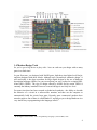
1.3 The DE2 board
The board you will be using for this project has an Altera Cyclone II EP2C35, which
contains 33K Logic elements (LEs), 105 M4K memory blocks, and 35 embedded
multipliers.
A diagram of the DE2 board is shown below. The board contains the FPGA, one static
RAM chip (512KB), some Flash RAM, an SDRAM chip, a video digital-to-analogue
converter (DAC), a PS/2 mouse/keyboard port and some other connections. Also
included is a USB port to allow you to program the FPGA and have access to various
components of the board from a PC.
Flash RAM is a type of RAM that does not lose its information when you turn the DE2
power off. We will use this to store any data we want to keep.
A full user-manual of the DE2 board can be downloaded from the project website or from
Altera’s website. This will be useful if you need to use some of the more advanced
features of the board.
3
4
M. Sonka, V. Hlavac and R. Boyle, “Image Processing, Analysis and Machine Vision”, ITP, 1993.
http://en.wikipedia.org/wiki/FPGA
3
1.4 Modern Design Tools
So you’ve got a big device to play with – how on earth can you design with so many
gates in so little time?
In your first term, you designed with NAND gates, built these into higher-level blocks,
and then designed with these blocks. Although such “hierarchical schematic design” is
still used today, it has been overtaken for large digital designs by the use of hardware
description languages (HDLs). In your second term you were exposed to a simple HDL,
Altera HDL (AHDL). The type of design offered by AHDL and its cousin VHDL is
currently the industry standard. However even such design is at a fairly low level.
For some time there has been research on behavioral synthesis – the ability to describe
the behavior of a circuit in a software-like notation, and then use the computer to
automatically build the circuit from gates. Recently some commercial products have
started to appear. One of these is called Handel-C, and allows you to design hardware in a
very similar way to programming in the language called C5.
5
B. Kernighan and D. Ritchie, “The C Programming Language”, Prentice-Hall, 1978.
4
2. Handel-C and the tools
For those of you familiar with C, you will see many similarities between Handel-C and
C. Those differences that do exist are because Handel-C is targeting hardware, whereas C
is targeting software. Those of you familiar only with Delphi will notice some syntactical
differences, although the basic concepts are the same. You may wish to look at a book on
C such as Kernighan and Ritchie.
We will go through three examples of Handel-C programs before setting you free to
implement your own.
2.1 Mouse movement
Our first example allows you to move a small 3x3-pixel pointer on the screen by moving
the mouse. The skills you will learn are:
• How a display works and how to interface with the DE2 display
• How to make your designs interactive by communicating with a mouse
• How to run portions of your code in parallel
The mouse movement code is shown below (note that C++ comment-style is allowed –
any text following “//” is a comment until the next line).
set clock = external "N2";
// Include libraries and headers
#include <stdlib.hch>
#include "DE2.hch"
// Some
#define
#define
#define
point
#define
RGB colour definitions
Green
0x00ff00
Black
0x000000
BALL_SIZE
5
// Size of ball - pixels to all sides of
BORDER
10
// size of border
// Structure for ball position
struct MovingParts
{
unsigned 10 BallX, BallY;
unsigned 10 BallEdgeLeft,BallEdgeRight,BallEdgeTop,BallEdgeBottom;
};
// Display the current mouse pointer position on the screen
macro proc Display(VideoPtr, BallPtr)
{
unsigned int 1 InBallX,InBallY;
while(1) {
// This executes in ONE CLOCK, so it sets the colour for EVERY
pixel
if (VideoPtr->Visible != 0) {
// Run all sections of code below in parallel
par {
5
//Are we in the ball (X direction)?
if( VideoPtr->ScanX == BallPtr->BallEdgeLeft)
InBallX = 1;
else
delay;
if( VideoPtr->ScanX == BallPtr->BallEdgeRight)
InBallX = 0;
else
delay;
//Are we in the ball (Y direction)?
if( VideoPtr->ScanY == BallPtr->BallEdgeTop)
InBallY = 1;
else
delay;
if( VideoPtr->ScanY == BallPtr->BallEdgeBottom)
InBallY = 0;
else
delay;
// Set the pixel colour, according to where we are
if ((InBallX == 1) && (InBallY == 1))
VideoPtr->Output = Green; // In the ball
else
// Make the background black
VideoPtr->Output = Black;
}
} else
// In the blanking period
delay;
}
}
macro proc PerFrameUpdate(VideoPtr, MousePtr, BallPtr)
{
do
{
// Wait until final scan line
while( !( (VideoPtr->ScanX==DE2VisibleCols) &&
(VideoPtr->ScanY==DE2VisibleLines - 1) ) )
delay;
// Update ball position
seq {
// Read mouse position
par {
BallPtr->BallX = MousePtr->PointerX;
BallPtr->BallY = MousePtr->PointerY;
}
par {
if( BallPtr->BallX > (DE2VisibleCols-BORDER) )
BallPtr->BallX = (DE2VisibleCols-BORDER);
else
6
delay;
if( BallPtr->BallY > (DE2VisibleLines-BORDER) )
BallPtr->BallY = (DE2VisibleLines-BORDER);
else
delay;
}
}
par { //update edge positions of ball, to be used in Display()
BallPtr->BallEdgeLeft = (BallPtr->BallX)-BALL_SIZE;
BallPtr->BallEdgeRight = (BallPtr->BallX)+BALL_SIZE;
BallPtr->BallEdgeTop = (BallPtr->BallY)-BALL_SIZE;
BallPtr->BallEdgeBottom = (BallPtr->BallY)+BALL_SIZE;
}
}while (1);
}
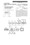
void main (void)
{
// Variables for mouse and video
DE2_PS2_MOUSE Mouse;
DE2_VGA_DRIVER Video;
struct MovingParts Ball;
par {
DE2PS2MouseDriver(&Mouse);
// Mouse interface
DE2VideoDriver800x600(&Video);
// Video driver
Display(&Video, &Ball);
// Main display process
PerFrameUpdate(&Video, &Mouse, &Ball);
// Update a frame
}
}
Let’s go through this code line-by-line and see how it works.
We start by defining some colors in terms of their Red-Green-Blue (RGB) values. These
are equivalent to global constant definitions in Delphi. The DE2 provides two fixed
clocks. A 27MHz clock is provided to FPGA pin D13, where a 50MHz clock is provided
to FPGA pin N2. Line “set clock = external "N2";” sets the clock to 50MHz. This is
essential if you want to use the VGA output driver with a resolution of 800x600.
Some “.hch” files are included next – you should always include these files which
contain essential definitions for the DE2 board.
Some final definitions include a size for our ball, 3 pixels, and a border width used to
stop the mouse going outside the edge of the screen.
A structure type is next defined (a structure is the C equivalent of a record in Delphi).
This contains six variables. BallX and BallY hold the current X and Y coordinates of the
ball. The remaining variables store the location on the screen of the top, left, bottom, and
right edges of the ball.
7
After the structure definition, the procedures are declared. Each starts with “macro proc”
and the procedure name, followed by the parameters of the procedure.
2.1.1 Display
The “Display” procedure is responsible for drawing the ball on the screen. It is passed a
pointer to the display driver (VideoPtr) and to a MovingParts structure (BallPtr).
The procedure starts by defining its local variables. The Delphi definition “var varname :
type;” is written in C as “type varname;”. The basic type supported by Handel-C, and the
type you must use for all your designs, is integer. Handel-C extends this type because for
hardware, we need to know how many bits each variable uses. In software the machine
for which we are compiling determines the number of bits. In our case, we define two
variables: InBallX and InBallY which will indicate whether the current pixel we are
drawing to the screen is inside the ball’s X and Y coordinate range. Since these are
Boolean values, we only require a single bit for storage. Thus we declare them as type
“unsigned int 1”, i.e. an unsigned integer one bit long.
The remainder of the procedure is a never-ending “while” loop (never ending because
“1” is always true). The while-loop is designed to take a single clock cycle to execute
because the DE2 needs a new pixel value to put to the screen every cycle. The screen has
a 800x600 visible resolution. Also, there are some pixels that belong to the so-called
“blanking period”.
The first thing the while-loop does is to distinguish between these two cases. “VideoPtr>Visible” accesses the “Visible” element of the structure pointed to by “VideoPtr”. The
DE2 display driver provides this variable to let us know whether we are in the blanking
period or not. If we are in the blanking period, we simply wait for a clock cycle before
going around the while loop again (the “else” clause). Otherwise we do several things.
The first four if-else statements see whether the current position on the screen in each
coordinate (e.g. VideoPtr->ScanX) corresponds to an edge of the ball. If so, it marks this
by setting the value of InBallX and InBallY appropriately. Finally, based on the value of
InBallX and InBallY, we decide whether to output a green pixel or a black pixel to the
display.
One detail which has been left out so far is the “par” construct. In order to get this loop to
run in a single clock cycle, we have decided to execute all the “if” statements, and their
associated instructions in parallel. This is because in Handel-C, each assignment takes
one clock cycle. We can do this because we’re designing hardware – all the compiler
needs to know is that it needs separate pieces of hardware to do each of the ifs rather than
doing each one in turn on the same piece of hardware like on your PC. One side-effect of
this is that the InBallX and InBallY variables tested by the final “if” statement are in
reality the InBallX and InBallY from the previous loop iteration, because the current ones
haven’t been written yet! You will be able to explore this point when trying out the
Handel-C debugging environment.
8
2.1.2 PerFrameUpdate
The remaining procedure, PerFrameUpdate, is responsible for updating the position of
the Ball on the screen, in response to mouse movements. Again, an infinite do-while loop
is used. Within this loop, the first action is to wait until the DE2 video driver has scanned
all the pixels on the screen, before it goes back to scan them once more. If we change the
ball during this time, when the screen is not being scanned, then we avoid flicker due to
the mouse moving while the mouse pointer is being drawn. You may wish to remove this
while loop and compare results.
Once we are in this time period, several operations are done sequentially (hence the “seq”
construct)6. First, we read the ball’s center position from the mouse (both X and Y are
read in parallel). Once this is done, we test to see if the X and Y positions go past a
border on the right and bottom of the screen. If they do, we correct them. Once again, the
correction is done in parallel. Finally, we update the left, right, top, and bottom edges of
the ball by adding or subtracting the appropriate constant to or from the center position.
The constants “DE2VisibleLines” and “DE2VisibleCols” have been defined in DE2.hch
header file and have values 600 and 800 respectively.
2.1.3 main
All C and Handel-C programs must have a “main” function. This is the function which is
run when the program starts up. main is declared to take no input parameters (void) and
return nothing. This will be the case with all hardware designs.
Three variables are declared: Mouse, Video, and Ball. These are structures containing the
DE2 mouse driver variables, the DE2 video driver variables and the ball parameters,
respectively. The first two structure types are built-in – the final one we defined at the
start of the program.
The main function itself simply consists of four parallel procedures. The DE2 mouse
driver, the DE2 display driver, our “Display” procedure, and our “PerFrameUpdate”
procedure. Note that to Display and PerFrameUpdate we pass the address the structures
(by prefixing the variable name with “&”). This is why we received pointers to structures
in the macro procedures themselves. This allows you to modify the parameters with
which you call the procedures (equivalent to “var” parameters in Delphi).
2.1.4 Setting up DK
We will now go step-by-step through the process of compiling your hardware design and
generating a circuit which will run on the DE2 board.
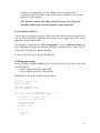
Start the DK software (Start > Celoxica > DK Design Suite > DK). This is Celoxica’s
integrated design and debugging suite for Handel-C. It is not dissimilar to other
development environments you may have experience with such as Borland’s Delphi
environment.
6
We could have left this out – statements execute sequentially unless otherwise specified. But if we needed
sequential execution within a parallel branch, we would need to use “seq”.
9
[If at this stage DK asks you about licensing, it means that DK has not been run yet this
year on your machine. You must select “Specify License Server”, and enter
[email protected] as the license server. This will only need to be done once for
each machine.]
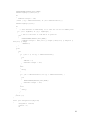
You need to create a project to hold your files for this example. Choose File > New.
Ensure the Project tab is active, Chip is highlighted. You need to tell to the compiler
which specific chip you are targeting. Select the “Altera Cyclone II Chip”. Browse for an
appropriate Location, such as a subdirectory from your home directory. Type
“de2project” as the Project Name, and click “OK”.
First, you need to specify the active configuration. This determines whether the output of
the compilation is for hardware design or simulation. At this stage we want to target an
actual hardware design. Select Build > Set Active Configuration > EDIF. EDIF is a fileformat used to store gate-level hardware designs.
Next you need to ensure that DK knows the location about the DE2 libraries. Select
Tools>Options, under the Directories tab add the de2lib folder and click OK. Now you
need to add the DE2 library. Select Project > Settings, under the Linker tab add de2.hcl
to the Object/library modules field (path: de2lib\de2.hcl). Also, add the stdlib.hcl file
(C:\program files\celoxica\pdk\hardware\lib\stdlib.hcl), which includes some useful
functions.
Now download the Handel-C file mouseproj.c, which we’ve been discussing, from
http://cas.ee.ic.ac.uk/people/ccb98/teaching/HandelC and save it into your project
directory. Add this file to your project by selecting Project > Add to Project > Files.
You will notice that the file mouseproj.c includes some header files other than the
DE2.hch (*.hch). You need to tell DK where to find these headers. Select Tools >
10
Options. Click on the Directory tab, make sure “Include Files” is highlighted, and click
“Add…”. Select the directory “C:\Program Files\Celoxica\PDK\Hardware\Include”.
The above steps are required only the first time that you set up the DK.
2.1.5 Compiling your program in DK
You are now in a position to compile your design. Choose Build > Build de2project. At
the bottom of the screen you can see the progress of DK. First the file is checked for
errors, and then a complete hardware design is constructed from NAND gates, Flip-Flops
and memory bits. You should see the following text eventually appear (the numbers may
vary):
NAND gates after compilation : 2891 (103 FFs, 0 memory bits)
NAND gates after optimisation : 2067 (72 FFs, 0 memory bits)
NAND gates after expansion : 2227 (71 FFs, 0 memory bits)
NAND gates after optimisation : 1802 (70 FFs, 0 memory bits)
LUTs after mapping
: 125 (70 FFs, 0 memory bits)
LUTs after post-optimisation : 125 (70 FFs, 0 memory bits)
0 errors, 0 warnings
DK initially constructed a design consisting of 2891 NAND gates, 103 flip-flops and 0
bits of RAM. After optimization, it has reduced this to 2067 NAND gates, 72 flip-flops
and 0 bits of RAM. DK also estimates that this design would require 125 4-input Lookup
Tables (LUTs) on the FPGA to implement. These 4-input 1-output ROMs are the basic
physical computational units in an FPGA.
If you examine your project directory with explorer, you will find that DK has created a
new subdirectory “EDIF” into which it has put the gate-level design.
In order to get the design onto the chip, a gate-level design is not enough. Each of the
gates must be mapped to a particular location on the FPGA, and the exact wiring
locations between each gate must be designed. For this we need the Altera tools.
2.1.6 Setting up Quartus II
Start up Altera Quartus II 8.0(Start->Programs->Altera->Quartus II->Quartus II). Select
File > New Project Wizard. Click Next. In “What is the working directory for this
project?” select your project directory and choose your EDIF folder created by DK(i.e.
C:\HandelC\Test\de2project\EDIF), and type “de2project” for “What is the name of this
Project?”. Click Next.
11
In the “File name” field for selecting the design that you want to include, browse and
select “mouse.edf” in the EDIF directory, click Add and then press “Next”.
Now select the Device Family “Cyclone II” select from the available devices
EP2C35F672C6, and click Next.
12
In the Design Entry/Synthesis select for “Tool name”: Custom, and “Format”: EDIF.
Click Next and then Click Finish.
Now, we need to specify the options for synthesis. Select Assignments->Settings, under
the EDA Tool Settings, click on Design Entry/Synthesis. In the “Library Mapping File”
field, browse for celoxica.lmf file (C:\Program Files\Celoxica\DK\Lmf\celoxica.lmf), and
click OK.
Also you need to set the unassigned pins to tri-state. Select Assignments->Device, click
on the Device & Pin Options button and select the unused pins tab. Set the unused pins
to: As input tri-stated, and press OK and OK.
You also need to tell to the tool where the DE2 libraries are. Go to Assignments>Settings and select Libraries. For the project library name browse for the de2lib () and
click on Add. Then OK.
Finally, the Altera tool does not know how fast you are indenting to clock your design (It
does not know about the DE2 board, just the targeted FPGA device). If you do not
specify a target clock frequency, then the tool will map your design to the FPGA put just
adequate effort. You can see how fast your design can be clocked after the compilation
under the Timing Analyzer summary. This should be more than 50MHz. It is better to tell
13
to the tool what the targeted clock frequency is in order to put more effort to achieve that.
This can be done through Assignments->Device, Timing Analysis Settings, Classic
Timing Analyzer Settings, under the Clock Settings box put 50 and click OK.
2.1.7 Compiling and Running the design
You only need to perform the step above only once. The steps mentioned in this section
are essential and need to be run every time you change the Handel-C design in DK.
1. Assign the FPGA pins. Select Tools=>Tcl Scripts and You are now in a position
to implement the design. Select under project the filename de2project.tcl and click
“RUN”.
2. Start Compilation (Processing->Start Compilation). This builds everything
necessary for loading your design on the DE2 board. The main window displays a
summary of the design implementation details. It tells you how much of the
FPGA your design has used, for example we used 346 out of the available 33,214
logic elements, less than 1% utilization.
An important part of the log the result from the “Classic Time Analysis”. Expand
this and click on “View Report”. Under “Summary” you will see a table with
paths that may violate your clock period. Now that the wiring has been
completed, the Altera tools can calculate how fast your circuit will go, and
whether that satisfies our target of a 50MHz clock. You should not get any
14
violation (A violation has a red color). Note: if you are using the mouse
component from the DE2 library, the tool will report a violation. You can safely
ignore this for the moment.
N.B.: Whether you meet this timing constraint on your own designs will
determine whether they will run as planned. Always check this!
2.1.8 Configure the FPGA
You are now in a position to load the FPGA on the DE2 board with your design. Make
sure your DE2 board has a ball-based PS2 mouse, a power supply unit, and a screen
plugged in. Switch on the RC100.
From Quartus II, right click on Tools->Programmer , click on Hardware Setup and
select USB-Blaster, tick the box “Program/Configure” and then click on “Start”. The file
“de2project.sof” holds your completed design.
Try now to move the mouse and see what happens.
2.2 Image processing
Our next example program FlashDisplay.hcc displays an image on the screen. The skills
you will learn are:
• How to read from the DE2 SRAM chip
• How to read from the DE2 Flash memory
The Handel-C code for this example is shown below.
set clock = external "N2";
#include "DE2.hch"
macro expr ImgWidth = 533;
macro expr ImgHeight = 400;
// ------------------ Output photo ----------------macro proc colorImg533x400(VideoPtr,SRAM)
{
macro expr sx = VideoPtr->ScanX;
macro expr sy = VideoPtr->ScanY;
unsigned 18 address;
unsigned 16 data;
unsigned 5 temp5;
par
{
address = 0;
temp5 = 0;
}
15
DE2ReadSRAM(address,data,SRAM);
DE2Set7SegDigit(1,data[3:0]);
do
{
VideoPtr->Output = 128;
}while ( (sy < DE2VisibleLines) && (sx < DE2VisibleCols) );
DE2Set7SegDigit(0,0x1);
do
{
// This executes in ONE CLOCK, so it sets the colour for EVERY pixel
if ( (sx < ImgWidth) && (sy < ImgHeight) )
{
// Run all sections of code below in parallel
par
{
DE2ReadSRAM(address,data,SRAM);
VideoPtr->Output = data[15:11] @ temp5 @ data[10:5] @ temp5<-4 @
data[4:0] @ temp5;
address++;
}
}
else
{
par
{
if ( (sx == 1) && (sy == DE2VisibleLines) )
{
par
{
address = 0;
VideoPtr->Output = 255;
}
}
else
{
delay;
}
if ( (sx == DE2VisibleCols) && (sy == DE2VisibleLines) )
{
par
{
DE2ReadSRAM(address,data,SRAM);
VideoPtr->Output = 255;
}
}
else
{
delay;
}
}
}
} while (1);
}
macro proc delayFunction(Ncycles)
{
unsigned 10 counter;
counter = 0;
do
16
{
counter++;
} while (counter < Ncycles);
}
// ---------- Preload a colour image from Flash memory to SRAM -------macro proc preLoadColorImg(SRAM,FLASH)
{
unsigned 22 FlashAddress;
unsigned 18 SRAMAddress;
unsigned 8 red,green,blue;
//RGB colour
unsigned 16 pixel;
unsigned 10 counter;
macro expr N=100;
par
{
FlashAddress = 0;
SRAMAddress =0;
counter = 0;
}
DE2Set7SegDigit(2,0x1);
do
{
counter++;
}while (counter < 1000);
DE2Set7SegDigit(3,0x2);
do
{
DE2ReadFLASH(FlashAddress,red,FLASH);
delayFunction(N);
FlashAddress++;
delayFunction(N);
DE2ReadFLASH(FlashAddress,green,FLASH);
delayFunction(N);
FlashAddress++;
delayFunction(N);
DE2ReadFLASH(FlashAddress,blue,FLASH);
delayFunction(N);
FlashAddress++;
delayFunction(N);
pixel = red[7:3]@green[7:2]@blue[7:3];
DE2WriteSRAM(SRAMAddress,pixel,SRAM);
SRAMAddress++;
delay;
} while (SRAMAddress < 213200);
DE2Set7SegDigit(4,0x3);
delay;
}
//---------------------------- MAIN PROGRAM -----------------------void main(void)
{
DE2SRAM SRAM;
DE2FLASH FLASH;
17
DE2_VGA_DRIVER Video;
unsigned 8 data;
unsigned 22 ImgAddr;
par
{
DE2SRAMDriver(&SRAM);
DE2FLASHDriver(&FLASH);
DE2VideoDriver800x600(&Video);
seq
{
preLoadColorImg(&SRAM,&FLASH);
colorImg533x400(&Video,&SRAM);
}
}
}
The two new components used in this example are the DE2 Flash RAM and the DE2
SRAM. The Flash RAM has a 22-bit address bus and an 8-bit data bus. The SRAM has a
18-bit address bus and a 16-bit data bus.
Examining “main”, we can see that the program loads an image from Flash into SRAM,
and then displays the image. We will consider each operation in turn.
2.2.1 Loading the image
Macro procedure preLoadColorImg loads this image from Flash into SRAM. The
procedure starts by defining several variables: a 22-bit flash address, an 18-bit ram
address, and three 8-bit values r, g, and b for red green and blue.
A do-while loop is responsible for loading the data into the SRAM. Three reads are
performed in sequence: red, green, and blue. Note that it is not possible to perform these
reads in parallel because you can only access one address of the RAM at one time – the
RAMs only have a single address and data bus. After reading each colour value, the three
8-bit values are combined into a 16-bit data value (after dropping some LSBs) and stored
at a location in the RAM. The Handel-C operator “@” simply combines bits together.
The entire loop is executed a total of 213,200 times. There is also a delay function
“delayFunction” called between readings from the FLASH. This is a limitation of the
current version of the library and it ensures that there is enough time to perform
successive readings from the FLASH.
2.2.2 Display
The final procedure is used to display the RAM bank on the display. The procedure
“colorImg533x400” starts by waiting for the Video Pointer to finish rendering the current
frame.
18
Several “macro expr” constructs are used essentially as short-hand notation. “macro expr
sx = VideoPtr->ScanX” means that in the following code one may write “sx” rather than
“VideoPtr->ScanX”.
While we are in the period where the image has to display the image on the screen (first
part of the if statement), the reading from the memory, the assignment to the Video
pointer and the increment of the memory address are happening in parallel. Thus, at cycle
N, we read pixel values from address K of the memory, we display the pixel values from
address K-1, and address variable becomes K+1.
When we are not in the period to display the image, we perform some initializations in
order to display the correct data when we return back to the display period.
You may notice some calls like “DE2Set7SegDigit(0,0x1)”. This displays a number in a
seven digit segment display, and can be used as a way to monitor the status of your
design on the FPGA. More information about this can be found in the Appendix.
2.2.3 Compiling your design
To ensure that you have fully grasped the process of generating and compiling a design
for
the
DE2,
downloaded
the
source
code
FlashDisplay.hcc
at:
http://cas.ee.ic.ac.uk/people/ccb98/teaching/HandelC and try it out. Note that you need to
load first the FLASH with the write image. Information about this is given in the
Appendix.
2.3
Simulation and Debugging
When you are designing your own hardware, it is useful to have a good debugger so that
you can catch bugs before trying your design on the DE2 board itself. DK includes an
integrated debugging environment, which we will now investigate.
Let’s do some more processing and not just display the input image. By adding the
following code, (and some extra variables), we can convert the image to BW:
…
if ( (sx < ImgWidth) && (sy < ImgHeight) )
{
// Run all sections of code below in parallel
par
{
DE2ReadSRAM(address,data,SRAM);
red = data[15:11] @ temp3;
green = data[10:5] @ temp2;
blue = data[4:0] @ temp3;
sum = adju(red,10) + adju(green,10) + adju(blue,10);
pixel = (sum/3);
VideoPtr->Output = pixel @ pixel @ pixel;
address++;
}
}
else…
19
The following declarations and initializations have been added:
unsigned 3 temp3;
unsigned 2 temp2;
unsigned 8 red, green, blue;
unsigned 10 sum;
unsigned 10 pixel;
par
{
address = 0;
temp3 = 0;
temp2 = 0;
}
The adju(x,N) macro, extends an unsigned variable x to N bits.
Although the DE2 board comes with simulation libraries, these are somewhat hard to use
so we suggest that debugging of your main algorithm should be done by separating it
from those parts of the code that are DE2-specific. Download the debug version of the
image processing example from: http://cas.ee.ic.ac.uk/people/ccb98/teaching/HandelC
This is a cut-down version, where the only remaining procedure is the one that actually
performs the image processing. Let’ call this procedure ProcessImage(). Rather than
using the DE2 on-board RAM, it has been replaced with a global “ram” variable, RAM.
It is declared to be an array of 128 16-bit values. We have used only 128 entries because
there is no need to simulate on a whole image. Because we use 128 entries, only a 7-bit
address bus is necessary, so address is now declared as “unsigned 7”. Also note that the
read from the DE2 RAM has been replaced with read from RAM. The remainder of the
code – that portion which actually performs the image processing – is identical.
Create a new project for this version. However this time select “Debug” rather than
“Edif” as the active configuration (Build > Set Active Configuration), and don’t include
DE2.hcl in Project > Settings > Linker (Do not forget to include the stdlib.hcl).
Build the project. You will now see some additional options in the Build menu, under
“Start Debug”. Select “Step into” or press F11. Just like in conventional development
environments such as the ARM SDK and Delphi, you can now single-step the execution
(F11/F10), set breakpoints (“hand” icon) and examine the value of variables as the
simulation runs (“watch” and “variables” icons). Click the “variables” icon and you will
see the variable RAM appear in the variables window. This is because RAM is the only
variable used in the current procedure (main). You can click on the “+” symbol next to
RAM to see all the values of RAM at the different array indices.
Several coloured arrows have appeared pointing at various lines of code. A green arrow
points to “main”, indicating that this is a currently executing function. A yellow arrow
marks the current execution point, whereas a grey arrow marks other lines of code that
20
will be executed simultaneously with the yellow line. The yellow and grey arrows
together point to the two parallel branches in the code, as expected.
Advance the execution by a single step (F11). The gray arrows indicate that all the
statements in the par{} block are executed in parallel. Keep pressing F11 and watch how
the variables change in the variable window. Now repeat the same, but comment out the
par keyword. In this case, the grey arrow does not re-appear because none of the
ProcessImage code is parallel. Keep pressing F11 and watch how the variables change in
the variable window.
2.4
Timing Problems
All the designs we have looked at so far have met the timing constraints and thus will
operate correctly with a 50MHz clock. We will now consider a case where this is not
true, in case you encounter one while developing your own designs.
Take the image processing example that converts a color image to B&W, and replace the
main code with the following code.
par
{
DE2ReadSRAM(address,data,SRAM);
rgb = (0 @ data[7:0]) * (0 @ data[7:0]) * (0 @ data[7:0]) * (0 @ data[7:0]);
VideoPtr->Output = rgb \\ 2;
// Drop the 2 LSBs
address++;
}
with the extra variable declaration:
unsigned 32 rgb;
This procedure finds the fourth power of the lower 8-bit combined RGB value stored in
SRAM, and stores the 32-bit result in rgb. The top 30 of these bits are passed to the video
pointer, by dropping the last 2 bits.
We are asking the FPGA to do a lot of computation in a single clock cycle: it must
multiply four 16-bit values together. Compiling this with DK will take (much!) longer
than with the other designs, but will not generate any errors. Now try running the Altera
tools on the resulting EDIF file. The tools will take a (very!) long time to complete, while
they try to place the LUTs on the FPGA and wire them up so that the design will run on a
50MHz clock. The Altera tools may also report success – but scroll up to the timing table
and you will see that the clock period has not been met (Timing Analyzer). Altera reports
this with a red colored message under the Timing Analyzer. If you have such a report,
your design will not work. (Note this is allowed in the mouse library).
DK has annotated the code so you can easily find where in your design this timing
violation is. At the point where the Altera tool reports the timing violation, it returns also
the associated path. This is captured in the columns “From” and “To”.
21
We can try to fix this problem by using an extra clock cycle, as below.
DE2ReadSRAM(address,data,SRAM);
//rgb = (0 @ data[7:0]) * (0 @ data[7:0]) * (0 @ data[7:0]) * (0 @ data[7:0]);
temp1 = (0 @ data[7:0]) * (0 @ data[7:0]);
rgb = (0 @ temp1) * (0 @ temp1);
VideoPtr->Output = rgb \\ 2;
// Drop the 2 LSBs
address++;
A new variable temp1 has been introduced as:
unsigned 16 temp1;
Compile the design in DK and Quartus II and check the final report from the Timing
Analyzer. This time, there is not any timing violation reported.
22
3. Some notes on Handel-C
3.1
Parallel versus Sequential
We will now investigate a few snippets of Handel-C code, which should illustrate some
of the differences between sequential and parallel execution.
int 4 a;
int 4 b;
signal int 4 a;
int 4 b;
int 4 a;
int 4 b;
signal int 4 a;
int 4 b;
…
…
…
…
seq {
a = b;
b = a;
}
(a)
seq {
a = b;
b = a;
}
(b)
par {
a = b;
b = a;
}
(c)
par {
a = b;
b = a;
}
(d)
Before the code portion of interest, let variable b have the value 1 and variable a have the
value 2.
In snippet (a), the code executes exactly as we would expect from a normal C program. a
gets set to the value 1 and then b gets set to the value 1. The execution takes 2 clock
cycles, one for each assignment.
Snippet (b) must be an error, because you are trying to read a signal a in a later clock
cycle than it is written. Signals can only be read in the same clock cycle.
In snippet (c), the two assignments execute in parallel. a gets set to the value 1 and b gets
set to the value 2. The two variables have been swapped, without the need for a
temporary variable. The whole execution takes a single cycle.
In snippet (d) signal a is assigned the value 1 and, on the same clock cycle, this new value
is assigned to variable b. At the end of the assignment, b holds the value 1. a will
continue to hold the value 1 only until the end of that clock cycle. The result, from b’s
perspective is the same as that of snippet (a) but overall execution takes only one cycle.
3.2 RAMs versus Arrays
In the debug version of the image processing example, we declared a RAM in Handel-C.
RAMs are like arrays, with the restriction that you cannot read or write to different
positions in a RAM during the same clock cycle. Arrays have no such restriction as they
are implemented differently in hardware. Arrays therefore typically require significantly
more resources in the FPGA. Consider a variable “A”. If A was declared as “ram
unsigned A[2]”, then the parallel code below would be incorrect. If A was declared as
“unsigned A[2]”, then the code would work without a problem.
par {
23
A[0] = x;
A[1] = y; }
3.2.1 Replicated par
Sometimes you may want to get the maximum parallelism out of an algorithm by using
“replicated par”. This is a version of par which can be thought of as a for-loop where all
iterations run in parallel. For example, the two pieces of code below have identical
meaning. (Note that a, b, and c must be arrays – not RAMs!)
par (i=0; i<3; i++) {
a[i] = b[i] + c[i];
}
par {
a[0] = b[0] + c[0];
a[1] = b[1] + c[1];
a[2] = b[2] + c[2];
}
3.3 Sources of additional information
If you require more information on Handel-C, the full language reference manual is
downloadable from the Celoxica website (http://www.celoxica.com). The DE2 manuals
are on every machine which has the DE2 support tools, in the “DE2_user_manual”
subdirectory of the DE2 installation directory.
4 Your assignment
Your assignment is to modify the image processing example to do something more
sophisticated or to write your own image processing design. The nature of your
modification is up to you. You may wish to consult some image processing books for
ideas, however please do not plan too hard a project. An ideal plan would be one with
stages, each one more complex than the next, so that you will have something to show at
the end even if you don’t manage to complete all stages. I suggest convolution masks as a
simple example which can be parallelized. An example sketch of a plan:
Week 1
Week 2
Week 3
Week 4
Perform edge detection using a 3x3 mask – write the Handel-C and get
it working in simulator
Get edge detection working on the DE2 board
Add some interactivity – edge detection only in a 50x50 pixel window
around the mouse pointer
Complete all loose ends and prepare for project presentation
There will be many possible solutions to any one problem. In order to achieve a good
quality solution, you should aim to make as much of the code run is parallel as possible,
in to get the best possible performance.
Our experience shows that there is a danger, if you are very confident in your software
skills, that you may interpret this project as a “software project” and thus plan something
too ambitious for efficient implementation directly in hardware.
Please keep your tutor aware of what you are planning, even before you hand-in your
report this term.
24
Please ensure that your interim report contains a breakdown of who will be doing
which part of the work.
5 Troubleshooting Guide
P. My design is taking an unusually long time to compile in DK.
A. Make sure you selected EDIF rather than DEBUG active configuration. You may be
trying to build a software debug model for the entire DE2!
P. My design is too big to fit into the device.
A. Try sharing hardware using functions (see Handel-C notes)
P. I have run out of disk space on my home directory.
A. Use C:\Temp as your project directory and only keep the source files and maybe the
configuration files (.sof) in your home directory.
Revision information
Major revision. ccb98 Feb 2009.New target device DE2 board. DK4.0, and Quartus II 8.0 are the tested tools.
Updated gac1 Dec 2002, gac1 Feb 2004, gac1 Jan 2005, amag97 Jan 2006, ccb98 Jan 2007, ccb98 Jan 2008
Original version: Created gac1 Jan 2002.
25
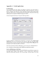
Appendix A – Useful Applications
Control Panel
You can download data and configure the different components of the DE2 board by
using the DE2_Control_Panel application (DE2\DE2_control_panel directory). First you
have to configure the FPGA to accept connections from the DE2_Control_Panel
application. This is done by configuring the FPGA with the DE2_USB_API.sof file. Drag
and Drop this file to Quartus II and then configure the FPGA.
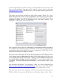
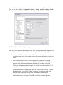
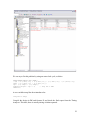
Click on the application and you will get the following window:
In order to establish a communication with the FPGA, you need to click on Open->Open
USB port 0. Now you can write/read to the memories, LEDs and LCD of the board.
After you finish you need to close the communication: on Open->Close USB port. More
information can be found in the DE2 User Manual.
Note: Due to the nature of the FLASH memory, you can write in it a limited number of
times. In order to write new data to the FLASH, you need first to erase it.
Convert a BMP picture to RAW data
If you want to download a picture in the FLASH/SRAM, you need first to convert it to
raw data (binary format). Altera provides a tool to achieve that: ImgConv.exe
(DE2\DE2_control_panel directory). This converts only a 640x480 image to raw data
26
that you can download through the control panel application to the board. More
information can be found in the DE2 User Manual.
If you need to convert an image of different size, you need to download the MATLAB
function ConvBMP2RAW.m from: http://cas.ee.ic.ac.uk/people/ccb98/teaching/HandelC.
The format of the RAW data is a raster scan of the original image stored as RGBRGB…,
where each color channel is 8 bits.
27
Appendix B – DE2 Handel-C Library
A document regarding the DE2 Handel-C library can be downloaded from:
http://cas.ee.ic.ac.uk/people/ccb98/teaching/HandelC.
Please not that the SDRAM access function does not work.
The DE2 Function Library was written by Mr. Vincent Lai.
28