1
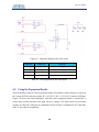
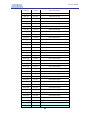
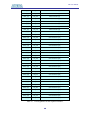
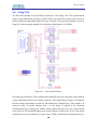
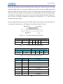
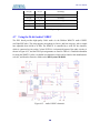
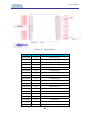
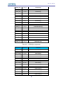
DE1 User Manual
Chapter 4
Using the DE1 Board
This chapter gives instructions for using the DE1 board and describes each of its I/O devices.
4.1 Configuring the Cyclone II FPGA
The procedure for downloading a circuit from a host computer to the DE1 board is described in the
tutorial Quartus II Introduction. This tutorial is found in the DE1_tutorials folder on the DE1
System CD-ROM, and it is also available on the Altera DE1 web pages. The user is encouraged to
read the tutorial first, and to treat the information below as a short reference.
The DE1 board contains a serial EEPROM chip that stores configuration data for the Cyclone II
FPGA. This configuration data is automatically loaded from the EEPROM chip into the FPGA each
time power is applied to the board. Using the Quartus II software, it is possible to reprogram the
FPGA at any time, and it is also possible to change the non-volatile data that is stored in the serial
EEPROM chip. Both types of programming methods are described below.
1. JTAG programming: In this method of programming, named after the IEEE standards Joint
Test Action Group, the configuration bit stream is downloaded directly into the Cyclone II
FPGA. The FPGA will retain this configuration as long as power is applied to the board;
the configuration is lost when the power is turned off.
2. AS programming: In this method, called Active Serial programming, the configuration bit
stream is downloaded into the Altera EPCS4 serial EEPROM chip. It provides non-volatile
storage of the bit stream, so that the information is retained even when the power supply to
the DE1 board is turned off. When the board's power is turned on, the configuration data in
the EPCS4 device is automatically loaded into the Cyclone II FPGA.
The sections below describe the steps used to perform both JTAG and AS programming. For both
methods the DE1 board is connected to a host computer via a USB cable. Using this connection, the
board will be identified by the host computer as an Altera USB Blaster device. The process for
installing on the host computer the necessary software device driver that communicates with the
USB Blaster is described in the tutorial Getting Started with Altera's DE1 Board. This tutorial is
available on the DE1 System CD-ROM and from the Altera DE1 web pages.
Configuring the FPGA in JTAG Mode
24
DE1 User Manual
Figure 4.1 illustrates the JTAG configuration setup. To download a configuration bit stream into the
Cyclone II FPGA, perform the following steps:
x
x
Ensure that power is applied to the DE1 board
Connect the supplied USB cable to the USB Blaster port on the DE1 board (see Figure 2.1)
x
Configure the JTAG programming circuit by setting the RUN/PROG switch (on the left side
of the board) to the RUN position.
x
The FPGA can now be programmed by using the Quartus II Programmer module to select a
configuration bit stream file with the .sof filename extension
USB Blaster Circuit
Quartus II
Programmer
USB
PROG/RUN
MAX
3128
"RUN"
JTAG Config Signals
JTAG UART
Auto
Power-on Config
JTAG Config Port
EPCS4
Serial
Configuration
Device
FPGA
Figure 4.1. The JTAG configuration scheme.
Configuring the EPCS4 in AS Mode
Figure 4.2 illustrates the AS configuration set up. To download a configuration bit stream into the
EPCS4 serial EEPROM device, perform the following steps:
x
x
x
Ensure that power is applied to the DE1 board
Connect the supplied USB cable to the USB Blaster port on the DE1 board (see Figure 2.1)
Configure the JTAG programming circuit by setting the RUN/PROG switch (on the left side
of the board) to the PROG position.
x
The EPCS4 chip can now be programmed by using the Quartus II Programmer module to
select a configuration bit stream file with the .pof filename extension
x
Once the programming operation is finished, set the RUN/PROG switch back to the RUN
position and then reset the board by turning the power switch off and back on; this action
causes the new configuration data in the EPCS4 device to be loaded into the FPGA chip.
25
DE1 User Manual
USB Blaster Circuit
RUN/PROG
Quartus II
Programmer
AS Mode
USB
AS Mode
Config
MAX
3128
"PROG"
Auto
Power-on Config
JTAG Config Port
EPCS4
Serial
Configuration
Device
FPGA
Figure 4.2. The AS configuration scheme.
In addition to its use for JTAG and AS programming, the USB Blaster port on the DE1 board can
also be used to control some of the board's features remotely from a host computer. Details that
describe this method of using the USB Blaster port are given in Chapter 3.
4.2 Using the LEDs and Switches
The DE1 board provides four pushbutton switches. Each of these switches is debounced using a
Schmitt Trigger circuit, as indicated in Figure 4.3. The four outputs called KEY0, …, KEY3 of the
Schmitt Trigger device are connected directly to the Cyclone II FPGA. Each switch provides a high
logic level (3.3 volts) when it is not pressed, and provides a low logic level (0 volts) when
depressed. Since the pushbutton switches are debounced, they are appropriate for use as clock or
reset inputs in a circuit.
Figure 4.3. Switch debouncing.
There are also 10 toggle switches (sliders) on the DE1 board. These switches are not debounced,
and are intended for use as level-sensitive data inputs to a circuit. Each switch is connected directly
to a pin on the Cyclone II FPGA. When a switch is in the DOWN position (closest to the edge of
the board) it provides a low logic level (0 volts) to the FPGA, and when the switch is in the UP
position it provides a high logic level (3.3 volts).
26
DE1 User Manual
There are 27 user-controllable LEDs on the DE1 board. Eighteen red LEDs are situated above the
18 toggle switches, and eight green LEDs are found above the pushbutton switches (the 9th green
LED is in the middle of the 7-segment displays). Each LED is driven directly by a pin on the
Cyclone II FPGA; driving its associated pin to a high logic level turns the LED on, and driving the
pin low turns it off. A schematic diagram that shows the pushbutton and toggle switches is given in
Figure 4.4. A schematic diagram that shows the LED circuitry appears in Figure 4.5.
A list of the pin names on the Cyclone II FPGA that are connected to the toggle switches is given in
Table 4.1. Similarly, the pins used to connect to the pushbutton switches and LEDs are displayed in
Tables 4.2 and 4.3, respectively.
Figure 4.4. Schematic diagram of the pushbutton and toggle switches.
27
DE1 User Manual
Figure 4.5. Schematic diagram of the LEDs.
Signal Name
FPGA Pin No.
Description
SW[0]
PIN_L22
Toggle Switch[0]
SW[1]
PIN_L21
Toggle Switch[1]
SW[2]
PIN_M22
Toggle Switch[2]
SW[3]
PIN_V12
Toggle Switch[3]
SW[4]
PIN_W12
Toggle Switch[4]
SW[5]
PIN_U12
Toggle Switch[5]
SW[6]
PIN_U11
Toggle Switch[6]
SW[7]
PIN_M2
Toggle Switch[7]
28
DE1 User Manual
SW[8]
PIN_M1
Toggle Switch[8]
SW[9]
PIN_L2
Toggle Switch[9]
Table 4.1. Pin assignments for the toggle switches.
Signal Name
FPGA Pin No.
Description
KEY[0]
PIN_R22
Pushbutton[0]
KEY[1]
PIN_R21
Pushbutton[1]
KEY[2]
PIN_T22
Pushbutton[2]
KEY[3]
PIN_T21
Pushbutton[3]
Table 4.2. Pin assignments for the pushbutton switches.
Signal Name
FPGA Pin No.
Description
LEDR[0]
PIN_R20
LED Red[0]
LEDR[1]
PIN_R19
LED Red[1]
LEDR[2]
PIN_U19
LED Red[2]
LEDR[3]
PIN_Y19
LED Red[3]
LEDR[4]
PIN_T18
LED Red[4]
LEDR[5]
PIN_V19
LED Red[5]
LEDR[6]
PIN_Y18
LED Red[6]
LEDR[7]
PIN_U18
LED Red[7]
LEDR[8]
PIN_R18
LED Red[8]
LEDR[9]
PIN_R17
LED Red[9]
LEDG[0]
PIN_U22
LED Green[0]
LEDG[1]
PIN_U21
LED Green[1]
LEDG[2]
PIN_V22
LED Green[2]
LEDG[3]
PIN_V21
LED Green[3]
LEDG[4]
PIN_W22
LED Green[4]
LEDG[5]
PIN_W21
LED Green[5]
LEDG[6]
PIN_Y22
LED Green[6]
LEDG[7]
PIN_Y21
LED Green[7]
Table 4.3. Pin assignments for the LEDs.
29
DE1 User Manual
4.3 Using the 7-segment Displays
The DE1 Board has four 7-segment displays. These displays are arranged into a group of four, with
the intent of displaying numbers of various sizes. As indicated in the schematic in Figure 4.6, the
seven segments are connected to pins on the Cyclone II FPGA. Applying a low logic level to a
segment causes it to light up, and applying a high logic level turns it off.
Each segment in a display is identified by an index from 0 to 6, with the positions given in Figure
4.7. Note that the dot in each display is unconnected and cannot be used. Table 4.4 shows the
assignments of FPGA pins to the 7-segment displays.
Figure 4.6. Schematic diagram of the 7-segment displays.
Figure 4.7. Position and index of each segment in a 7-segment display.
30
DE1 User Manual
Signal Name
FPGA Pin No.
Description
HEX0[0]
PIN_J2
Seven Segment Digit 0[0]
HEX0[1]
PIN_J1
Seven Segment Digit 0[1]
HEX0[2]
PIN_H2
Seven Segment Digit 0[2]
HEX0[3]
PIN_H1
Seven Segment Digit 0[3]
HEX0[4]
PIN_F2
Seven Segment Digit 0[4]
HEX0[5]
PIN_F1
Seven Segment Digit 0[5]
HEX0[6]
PIN_E2
Seven Segment Digit 0[6]
HEX1[0]
PIN_E1
Seven Segment Digit 1[0]
HEX1[1]
PIN_H6
Seven Segment Digit 1[1]
HEX1[2]
PIN_H5
Seven Segment Digit 1[2]
HEX1[3]
PIN_H4
Seven Segment Digit 1[3]
HEX1[4]
PIN_G3
Seven Segment Digit 1[4]
HEX1[5]
PIN_D2
Seven Segment Digit 1[5]
HEX1[6]
PIN_D1
Seven Segment Digit 1[6]
HEX2[0]
PIN_G5
Seven Segment Digit 2[0]
HEX2[1]
PIN_G6
Seven Segment Digit 2[1]
HEX2[2]
PIN_C2
Seven Segment Digit 2[2]
HEX2[3]
PIN_C1
Seven Segment Digit 2[3]
HEX2[4]
PIN_E3
Seven Segment Digit 2[4]
HEX2[5]
PIN_E4
Seven Segment Digit 2[5]
HEX2[6]
PIN_D3
Seven Segment Digit 2[6]
HEX3[0]
PIN_F4
Seven Segment Digit 3[0]
HEX3[1]
PIN_D5
Seven Segment Digit 3[1]
HEX3[2]
PIN_D6
Seven Segment Digit 3[2]
HEX3[3]
PIN_J4
Seven Segment Digit 3[3]
HEX3[4]
PIN_L8
Seven Segment Digit 3[4]
HEX3[5]
PIN_F3
Seven Segment Digit 3[5]
HEX3[6]
PIN_D4
Seven Segment Digit 3[6]
Table 4.4. Pin assignments for the 7-segment displays.
4.4 Clock Inputs
The DE1 board includes three oscillators that produce 27 MHz, 24Mhz, and 50 MHz clock signals.
The board also includes an SMA connector which can be used to connect an external clock source
to the board. The schematic of the clock circuitry is shown in Figure 4.8, and the associated pin
assignments appear in Table 4.5.
31
DE1 User Manual
Figure 4.8. Schematic diagram of the clock circuit.
Signal Name
FPGA Pin No.
Description
CLOCK_27
PIN_D12, PIN_E12
27 MHz clock input
CLOCK_50
PIN_L1
50 MHz clock input
CLOCK_24
PIN_A12, PIN_B12
24 MHz clock input from USB Blaster
EXT_CLOCK
PIN_M21
External (SMA) clock input
Table 4.5. Pin assignments for the clock inputs.
4.5 Using the Expansion Header
The DE1 Board provides two 40-pin expansion headers. Each header connects directly to 36 pins on
the Cyclone II FPGA, and also provides DC +5V (VCC5), DC +3.3V (VCC33), and two GND pins.
Figure 4.10 shows the related schematics. Each pin on the expansion headers is connected to a
resistor that provide protection from high and low voltages. The figure shows the protection
circuitry for only four of the pins on each header, but this circuitry is included for all 72 data pins.
Table 4.7 gives the pin assignments.
32
DE1 User Manual
Figure 4.10. Schematic diagram of the expansion headers.
Signal Name
FPGA Pin No.
Description
GPIO_0[0]
PIN_A13
GPIO Connection 0[0]
33
DE1 User Manual
GPIO_0[1]
PIN_B13
GPIO Connection 0[1]
GPIO_0[2]
PIN_A14
GPIO Connection 0[2]
GPIO_0[3]
PIN_B14
GPIO Connection 0[3]
GPIO_0[4]
PIN_A15
GPIO Connection 0[4]
GPIO_0[5]
PIN_B15
GPIO Connection 0[5]
GPIO_0[6]
PIN_A16
GPIO Connection 0[6]
GPIO_0[7]
PIN_B16
GPIO Connection 0[7]
GPIO_0[8]
PIN_A17
GPIO Connection 0[8]
GPIO_0[9]
PIN_B17
GPIO Connection 0[9]
GPIO_0[10]
PIN_A18
GPIO Connection 0[10]
GPIO_0[11]
PIN_B18
GPIO Connection 0[11]
GPIO_0[12]
PIN_A19
GPIO Connection 0[12]
GPIO_0[13]
PIN_B19
GPIO Connection 0[13]
GPIO_0[14]
PIN_A20
GPIO Connection 0[14]
GPIO_0[15]
PIN_B20
GPIO Connection 0[15]
GPIO_0[16]
PIN_C21
GPIO Connection 0[16]
GPIO_0[17]
PIN_C22
GPIO Connection 0[17]
GPIO_0[18]
PIN_D21
GPIO Connection 0[18]
GPIO_0[19]
PIN_D22
GPIO Connection 0[19]
GPIO_0[20]
PIN_E21
GPIO Connection 0[20]
GPIO_0[21]
PIN_E22
GPIO Connection 0[21]
GPIO_0[22]
PIN_F21
GPIO Connection 0[22]
GPIO_0[23]
PIN_F22
GPIO Connection 0[23]
GPIO_0[24]
PIN_G21
GPIO Connection 0[24]
GPIO_0[25]
PIN_G22
GPIO Connection 0[25]
GPIO_0[26]
PIN_J21
GPIO Connection 0[26]
GPIO_0[27]
PIN_J22
GPIO Connection 0[27]
GPIO_0[28]
PIN_K21
GPIO Connection 0[28]
GPIO_0[29]
PIN_K22
GPIO Connection 0[29]
GPIO_0[30]
PIN_J19
GPIO Connection 0[30]
GPIO_0[31]
PIN_J20
GPIO Connection 0[31]
GPIO_0[32]
PIN_J18
GPIO Connection 0[32]
GPIO_0[33]
PIN_K20
GPIO Connection 0[33]
GPIO_0[34]
PIN_L19
GPIO Connection 0[34]
GPIO_0[35]
PIN_L18
GPIO Connection 0[35]
GPIO_1[0]
PIN_H12
GPIO Connection 1[0]
GPIO_1[1]
PIN_H13
GPIO Connection 1[1]
34
DE1 User Manual
GPIO_1[2]
PIN_H14
GPIO Connection 1[2]
GPIO_1[3]
PIN_G15
GPIO Connection 1[3]
GPIO_1[4]
PIN_E14
GPIO Connection 1[4]
GPIO_1[5]
PIN_E15
GPIO Connection 1[5]
GPIO_1[6]
PIN_F15
GPIO Connection 1[6]
GPIO_1[7]
PIN_G16
GPIO Connection 1[7]
GPIO_1[8]
PIN_F12
GPIO Connection 1[8]
GPIO_1[9]
PIN_F13
GPIO Connection 1[9]
GPIO_1[10]
PIN_C14
GPIO Connection 1[10]
GPIO_1[11]
PIN_D14
GPIO Connection 1[11]
GPIO_1[12]
PIN_D15
GPIO Connection 1[12]
GPIO_1[13]
PIN_D16
GPIO Connection 1[13]
GPIO_1[14]
PIN_C17
GPIO Connection 1[14]
GPIO_1[15]
PIN_C18
GPIO Connection 1[15]
GPIO_1[16]
PIN_C19
GPIO Connection 1[16]
GPIO_1[17]
PIN_C20
GPIO Connection 1[17]
GPIO_1[18]
PIN_D19
GPIO Connection 1[18]
GPIO_1[19]
PIN_D20
GPIO Connection 1[19]
GPIO_1[20]
PIN_E20
GPIO Connection 1[20]
GPIO_1[21]
PIN_F20
GPIO Connection 1[21]
GPIO_1[22]
PIN_E19
GPIO Connection 1[22]
GPIO_1[23]
PIN_E18
GPIO Connection 1[23]
GPIO_1[24]
PIN_G20
GPIO Connection 1[24]
GPIO_1[25]
PIN_G18
GPIO Connection 1[25]
GPIO_1[26]
PIN_G17
GPIO Connection 1[26]
GPIO_1[27]
PIN_H17
GPIO Connection 1[27]
GPIO_1[28]
PIN_J15
GPIO Connection 1[28]
GPIO_1[29]
PIN_H18
GPIO Connection 1[29]
GPIO_1[30]
PIN_N22
GPIO Connection 1[30]
GPIO_1[31]
PIN_N21
GPIO Connection 1[31]
GPIO_1[32]
PIN_P15
GPIO Connection 1[32]
GPIO_1[33]
PIN_N15
GPIO Connection 1[33]
GPIO_1[34]
PIN_P17
GPIO Connection 1[34]
GPIO_1[35]
PIN_P18
GPIO Connection 1[35]
Table 4.7. Pin assignments for the expansion headers.
35
DE1 User Manual
4.6 Using VGA
The DE1 board includes a 16-pin D-SUB connector for VGA output. The VGA synchronization
signals are provided directly from the Cyclone II FPGA, and a 4-bit DAC using resistor network is
used to produce the analog data signals (red, green, and blue). The associated schematic is given in
Figure 4.11 and can support standard VGA resolution (640x480 pixels, at 25 MHz).
Figure 4.11. VGA circuit schematic.
The timing specification for VGA synchronization and RGB (red, green, blue) data can be found on
various educational web sites (for example, search for “VGA signal timing”). Figure 4.12 illustrates
the basic timing requirements for each row (horizontal) that is displayed on a VGA monitor. An
active-low pulse of specific duration (time a in the figure) is applied to the horizontal
synchronization (hsync) input of the monitor, which signifies the end of one row of data and the
start of the next. The data (RGB) inputs on the monitor must be off (driven to 0 V) for a time period
called the back porch (b) after the hsync pulse occurs, which is followed by the display interval (c).
36
DE1 User Manual
During the data display interval the RGB data drives each pixel in turn across the row being
displayed. Finally, there is a time period called the front porch (d) where the RGB signals must
again be off before the next hsync pulse can occur. The timing of the vertical synchronization (vsync)
is the same as shown in Figure 4.12, except that a vsync pulse signifies the end of one frame and the
start of the next, and the data refers to the set of rows in the frame (horizontal timing). Figures 4.13
and 4.14 show, for different resolutions, the durations of time periods a, b, c, and d for both
horizontal and vertical timing.
The pin assignments between the Cyclone II FPGA and the VGA connector are listed in Table 4.8.
An example of code that drives a VGA display is described in Sections 5.2 and 5.3.
Figure 4.12. VGA horizontal timing specification.
VGA mode
Horizontal Timing Spec
Configuration
Resolution(HxV)
a(us)
b(us)
c(us)
d(us)
VGA(60Hz)
640x480
3.8
1.9
25.4
0.6
Pixel clock(Mhz)
25
(640/c)
Figure 4.13. VGA horizontal timing specification.
VGA mode
Configuration
VGA(60Hz)
Vertical Timing Spec
Resolution
(HxV)
a(lines)
b(lines)
c(lines)
d(lines)
2
33
480
10
640x480
Figure 4.14. VGA vertical timing specification.
Signal Name
FPGA Pin No.
Description
VGA_R[0]
PIN_D9
VGA Red[0]
VGA_R[1]
PIN_C9
VGA Red[1]
VGA_R[2]
PIN_A7
VGA Red[2]
VGA_R[3]
PIN_B7
VGA Red[3]
VGA_G[0]
PIN_B8
VGA Green[0]
VGA_G[1]
PIN_C10
VGA Green[1]
VGA_G[2]
PIN_B9
VGA Green[2]
VGA_G[3]
PIN_A8
VGA Green[3]
37
DE1 User Manual
VGA_B[0]
PIN_A9
VGA Blue[0]
VGA_B[1]
PIN_D11
VGA Blue[1]
VGA_B[2]
PIN_A10
VGA Blue[2]
VGA_B[3]
PIN_B10
VGA Blue[3]
VGA_HS
PIN_A11
VGA H_SYNC
VGA_VS
PIN_B11
VGA V_SYNC
Table 4.8. ADV7123 pin assignments.
4.7 Using the 24-bit Audio CODEC
The DE1 board provides high-quality 24-bit audio via the Wolfson WM8731 audio CODEC
(enCOder/DECoder). This chip supports microphone-in, line-in, and line-out ports, with a sample
rate adjustable from 8 kHz to 96 kHz. The WM8731 is controlled by a serial I2C bus interface,
which is connected to pins on the Cyclone II FPGA. A schematic diagram of the audio circuitry is
shown in Figure 4.15, and the FPGA pin assignments are listed in Table 4.9. Detailed information
for using the WM8731 codec is available in its datasheet, which can be found on the manufacturer's
web site, and from the Datasheet folder on the DE1 System CD-ROM.
Figure 4.15. Audio CODEC schematic.
38
DE1 User Manual
Signal Name
FPGA Pin No.
Description
AUD_ADCLRCK
PIN_A6
Audio CODEC ADC LR Clock
AUD_ADCDAT
PIN_B6
Audio CODEC ADC Data
AUD_DACLRCK
PIN_A5
Audio CODEC DAC LR Clock
AUD_DACDAT
PIN_B5
Audio CODEC DAC Data
AUD_XCK
PIN_B4
Audio CODEC Chip Clock
AUD_BCLK
PIN_A4
Audio CODEC Bit-Stream Clock
I2C_SCLK
PIN_A3
I2C Data
I2C_SDAT
PIN_B3
I2C Clock
Table 4.9. Audio CODEC pin assignments.
4.8 RS-232 Serial Port
The DE1 board uses the MAX232 transceiver chip and a 9-pin D-SUB connector for RS-232
communications. For detailed information on how to use the transceiver refer to the datasheet,
which is available on the manufacturer’s web site, and from the Datasheet folder on the DE1
System CD-ROM. Figure 4.16 shows the related schematics, and Table 4.10 lists the Cyclone II
FPGA pin assignments.
Figure 4.16. MAX232 (RS-232) chip schematic.
Signal Name
FPGA Pin No.
Description
UART_RXD
PIN_F14
UART Receiver
UART_TXD
PIN_G12
UART Transmitter
Table 4.10. RS-232 pin assignments.
39
DE1 User Manual
4.9 PS/2 Serial Port
The DE1 board includes a standard PS/2 interface and a connector for a PS/2 keyboard or mouse.
Figure 4.17 shows the schematic of the PS/2 circuit. Instructions for using a PS/2 mouse or
keyboard can be found by performing an appropriate search on various educational web sites. The
pin assignments for the associated interface are shown in Table 4.11.
Figure 4.17. PS/2 schematic.
Signal Name
FPGA Pin No.
Description
PS2_CLK
PIN_H15
PS/2 Clock
PS2_DAT
PIN_J14
PS/2 Data
Table 4.11. PS/2 pin assignments.
4.10 Using SDRAM/SRAM/Flash
The DE1 board provides an 8-Mbyte SDRAM, 512-Kbyte SRAM, and 4-Mbyte (1-Mbyte on some
boards) Flash memory. Figures 4.23, 4.24, and 4.25 show the schematics of the memory chips. The
pin assignments for each device are listed in Tables 4.16, 4.17, and 4.18. The datasheets for the
memory chips are provided in the Datasheet folder on the DE1 System CD-ROM.
40
DE1 User Manual
Figure 4.23.
Figure 4.24.
SDRAM schematic.
SRAM schematic.
41
DE1 User Manual
Figure 4.25.
Flash schematic.
Signal Name
FPGA Pin No.
Description
DRAM_ADDR[0]
PIN_W4
SDRAM Address[0]
DRAM_ADDR[1]
PIN_W5
SDRAM Address[1]
DRAM_ADDR[2]
PIN_Y3
SDRAM Address[2]
DRAM_ADDR[3]
PIN_Y4
SDRAM Address[3]
DRAM_ADDR[4]
PIN_R6
SDRAM Address[4]
DRAM_ADDR[5]
PIN_R5
SDRAM Address[5]
DRAM_ADDR[6]
PIN_P6
SDRAM Address[6]
DRAM_ADDR[7]
PIN_P5
SDRAM Address[7]
DRAM_ADDR[8]
PIN_P3
SDRAM Address[8]
DRAM_ADDR[9]
PIN_N4
SDRAM Address[9]
DRAM_ADDR[10]
PIN_W3
SDRAM Address[10]
DRAM_ADDR[11]
PIN_N6
SDRAM Address[11]
DRAM_DQ[0]
PIN_U1
SDRAM Data[0]
DRAM_DQ[1]
PIN_U2
SDRAM Data[1]
DRAM_DQ[2]
PIN_V1
SDRAM Data[2]
DRAM_DQ[3]
PIN_V2
SDRAM Data[3]
DRAM_DQ[4]
PIN_W1
SDRAM Data[4]
DRAM_DQ[5]
PIN_W2
SDRAM Data[5]
DRAM_DQ[6]
PIN_Y1
SDRAM Data[6]
42
DE1 User Manual
DRAM_DQ[7]
PIN_Y2
SDRAM Data[7]
DRAM_DQ[8]
PIN_N1
SDRAM Data[8]
DRAM_DQ[9]
PIN_N2
SDRAM Data[9]
DRAM_DQ[10]
PIN_P1
SDRAM Data[10]
DRAM_DQ[11]
PIN_P2
SDRAM Data[11]
DRAM_DQ[12]
PIN_R1
SDRAM Data[12]
DRAM_DQ[13]
PIN_R2
SDRAM Data[13]
DRAM_DQ[14]
PIN_T1
SDRAM Data[14]
DRAM_DQ[15]
PIN_T2
SDRAM Data[15]
DRAM_BA_0
PIN_U3
SDRAM Bank Address[0]
DRAM_BA_1
PIN_V4
SDRAM Bank Address[1]
DRAM_LDQM
PIN_R7
SDRAM Low-byte Data Mask
DRAM_UDQM
PIN_M5
SDRAM High-byte Data Mask
DRAM_RAS_N
PIN_T5
SDRAM Row Address Strobe
DRAM_CAS_N
PIN_T3
SDRAM Column Address Strobe
DRAM_CKE
PIN_N3
SDRAM Clock Enable
DRAM_CLK
PIN_U4
SDRAM Clock
DRAM_WE_N
PIN_R8
SDRAM Write Enable
DRAM_CS_N
PIN_T6
SDRAM Chip Select
Table 4.16. SDRAM pin assignments.
Signal Name
FPGA Pin No.
Description
SRAM_ADDR[0]
PIN_AA3
SRAM Address[0]
SRAM_ADDR[1]
PIN_AB3
SRAM Address[1]
SRAM_ADDR[2]
PIN_AA4
SRAM Address[2]
SRAM_ADDR[3]
PIN_AB4
SRAM Address[3]
SRAM_ADDR[4]
PIN_AA5
SRAM Address[4]
SRAM_ADDR[5]
PIN_AB10
SRAM Address[5]
SRAM_ADDR[6]
PIN_AA11
SRAM Address[6]
SRAM_ADDR[7]
PIN_AB11
SRAM Address[7]
SRAM_ADDR[8]
PIN_V11
SRAM Address[8]
SRAM_ADDR[9]
PIN_W11
SRAM Address[9]
SRAM_ADDR[10]
PIN_R11
SRAM Address[10]
SRAM_ADDR[11]
PIN_T11
SRAM Address[11]
SRAM_ADDR[12]
PIN_Y10
SRAM Address[12]
SRAM_ADDR[13]
PIN_U10
SRAM Address[13]
43
DE1 User Manual
SRAM_ADDR[14]
PIN_R10
SRAM Address[14]
SRAM_ADDR[15]
PIN_T7
SRAM Address[15]
SRAM_ADDR[16]
PIN_Y6
SRAM Address[16]
SRAM_ADDR[17]
PIN_Y5
SRAM Address[17]
SRAM_DQ[0]
PIN_AA6
SRAM Data[0]
SRAM_DQ[1]
PIN_AB6
SRAM Data[1]
SRAM_DQ[2]
PIN_AA7
SRAM Data[2]
SRAM_DQ[3]
PIN_AB7
SRAM Data[3]
SRAM_DQ[4]
PIN_AA8
SRAM Data[4]
SRAM_DQ[5]
PIN_AB8
SRAM Data[5]
SRAM_DQ[6]
PIN_AA9
SRAM Data[6]
SRAM_DQ[7]
PIN_AB9
SRAM Data[7]
SRAM_DQ[8]
PIN_Y9
SRAM Data[8]
SRAM_DQ[9]
PIN_W9
SRAM Data[9]
SRAM_DQ[10]
PIN_V9
SRAM Data[10]
SRAM_DQ[11]
PIN_U9
SRAM Data[11]
SRAM_DQ[12]
PIN_R9
SRAM Data[12]
SRAM_DQ[13]
PIN_W8
SRAM Data[13]
SRAM_DQ[14]
PIN_V8
SRAM Data[14]
SRAM_DQ[15]
PIN_U8
SRAM Data[15]
SRAM_WE_N
PIN_AA10
SRAM Write Enable
SRAM_OE_N
PIN_T8
SRAM Output Enable
SRAM_UB_N
PIN_W7
SRAM High-byte Data Mask
SRAM_LB_N
PIN_Y7
SRAM Low-byte Data Mask
SRAM_CE_N
PIN_AB5
SRAM Chip Enable
Table 4.17. SRAM pin assignments.
Signal Name
FPGA Pin No.
Description
FL_ADDR[0]
PIN_AB20
FLASH Address[0]
FL_ADDR[1]
PIN_AA14
FLASH Address[1]
FL_ADDR[2]
PIN_Y16
FLASH Address[2]
FL_ADDR[3]
PIN_R15
FLASH Address[3]
FL_ADDR[4]
PIN_T15
FLASH Address[4]
FL_ADDR[5]
PIN_U15
FLASH Address[5]
FL_ADDR[6]
PIN_V15
FLASH Address[6]
FL_ADDR[7]
PIN_W15
FLASH Address[7]
44
DE1 User Manual
FL_ADDR[8]
PIN_R14
FLASH Address[8]
FL_ADDR[9]
PIN_Y13
FLASH Address[9]
FL_ADDR[10]
PIN_R12
FLASH Address[10]
FL_ADDR[11]
PIN_T12
FLASH Address[11]
FL_ADDR[12]
PIN_AB14
FLASH Address[12]
FL_ADDR[13]
PIN_AA13
FLASH Address[13]
FL_ADDR[14]
PIN_AB13
FLASH Address[14]
FL_ADDR[15]
PIN_AA12
FLASH Address[15]
FL_ADDR[16]
PIN_AB12
FLASH Address[16]
FL_ADDR[17]
PIN_AA20
FLASH Address[17]
FL_ADDR[18]
PIN_U14
FLASH Address[18]
FL_ADDR[19]
PIN_V14
FLASH Address[19]
FL_ADDR[20]
PIN_U13
FLASH Address[20]
FL_ADDR[21]
PIN_R13
FLASH Address[21]
FL_DQ[0]
PIN_AB16
FLASH Data[0]
FL_DQ[1]
PIN_AA16
FLASH Data[1]
FL_DQ[2]
PIN_AB17
FLASH Data[2]
FL_DQ[3]
PIN_AA17
FLASH Data[3]
FL_DQ[4]
PIN_AB18
FLASH Data[4]
FL_DQ[5]
PIN_AA18
FLASH Data[5]
FL_DQ[6]
PIN_AB19
FLASH Data[6]
FL_DQ[7]
PIN_AA19
FLASH Data[7]
FL_OE_N
PIN_AA15
FLASH Output Enable
FL_RST_N
PIN_W14
FLASH Reset
FL_WE_N
PIN_Y14
FLASH Write Enable
Table 4.18. Flash pin assignments.
45