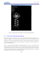
1
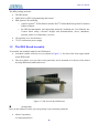
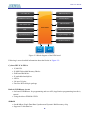
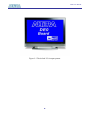
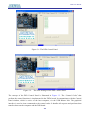
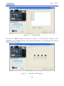
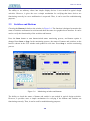
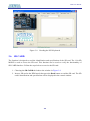
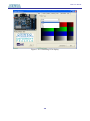
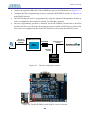
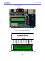
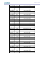
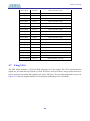
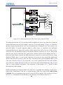
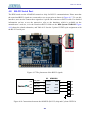
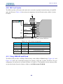
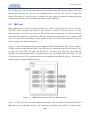
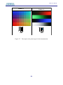
Altera DE0 Board Version 1.00 Copyright © 2009 Terasic Technologies Altera DE0 Board CONTENTS Chapter 1 DE0 Package ..................................................................................................................... 1 1.1 1.2 Package Contents ................................................................................................................. 1 The DE0 Board Assembly.................................................................................................... 2 Getting Help ......................................................................................................................... 2 Chapter 2 Altera DE0 Board ............................................................................................................. 4 2.1 2.2 2.3 Layout and Components ...................................................................................................... 4 Block Diagram of the DE0 Board ........................................................................................ 5 Power-up the DE0 Board ..................................................................................................... 8 Chapter 3 DE0 Control Panel ......................................................................................................... 10 3.1 3.2 3.3 3.4 3.5 3.6 3.7 Control Panel Setup ........................................................................................................... 10 Controlling the LEDs and 7-Segment Displays ................................................................. 12 Switches and Buttons ......................................................................................................... 14 SDRAM and Flash Controller and Programmer ................................................................ 15 PS2 Device ......................................................................................................................... 16 SD CARD .......................................................................................................................... 17 VGA ................................................................................................................................... 18 Chapter 4 Using the DE0 Board ..................................................................................................... 20 4.1 4.2 4.3 4.4 4.5 4.6 4.7 4.8 Configuring the Cyclone III FPGA .................................................................................... 20 Using the LEDs and Switches ............................................................................................ 23 Using the 7-segment Displays............................................................................................ 26 Clock Circuitry................................................................................................................... 28 Using the LCD Module ...................................................................................................... 29 Using the Expansion Header .............................................................................................. 31 Using VGA ........................................................................................................................ 34 RS-232 Serial Port ............................................................................................................. 37 4.9 4.10 4.11 PS/2 Serial Port .................................................................................................................. 38 SD Card Socket .................................................................................................................. 39 Using SDRAM and Flash .................................................................................................. 39 Chapter 5 Examples of Advanced Demonstrations ...................................................................... 44 5.1 5.2 5.3 DE0 Factory Configuration ................................................................................................ 44 SD Card .............................................................................................................................. 45 VGA Color Pattern Demonstration .................................................................................... 49 Chapter 6 Appendix ......................................................................................................................... 53 6.1 Revision History ................................................................................................................ 53 ii Altera DE0 Board 6.2 Copyright Statement .......................................................................................................... 53 iii DE0 User Manual Chapter 1 DE0 Package The DE0 package contains all the components needed to use the DE0 board in conjunction with a computer that runs the Microsoft Windows software. 1.1 Package Contents Figure 1-1shows a photograph of the DE0 package. Figure 1-1 The DE0 package contents. 1 DE0 User Manual The DE0 package includes: The DE0 board USB Cable for FPGA programming and control DE0 System CD containing : o Altera’s Quartus® II Web Edition and the Nios® II Embedded Design Suit Evaluation Edition software o the DE0 documentation and supporting materials, including the User Manual, the Control Panel utility, reference designs and demonstrations, device datasheets, tutorials, and a set of laboratory exercises Clear plastic cover for the board 7.5 DC wall-mount power supply 1.2 The DE0 Board Assembly To assemble the included stands for the DE0 board: Assemble a rubber (silicon) cover, as shown in Figure 1-2, for each of the four copper stands on the DE0 board The clear plastic cover provides extra protection, and is mounted over the top of the board by using additional stands and screws Figure 1-2 The feet for the DE0 board. Getting Help Here are the addresses where you can get help if you encounter problems: Altera Corporation 101 Innovation Drive 2 DE0 User Manual San Jose, California, 95134 USA Email: [email protected] Terasic Technologies No. 356, Sec. 1, Fusing E. Rd. Jhubei City, HsinChu County, Taiwan, 302 Email: [email protected] Web: DE0.terasic.com 3 DE0 User Manual Chapter 2 Altera DE0 Board This chapter presents the features and design characteristics of the DE0 board. 2.1 Layout and Components A photograph of the DE0 board is shown in Figure 2-1. It depicts the layout of the board and indicates the location of the connectors and key components. Power Supply Input USB Blaster Connector Triple 4 - bit VGA DAC PS/2 Port SD Card Socket RS - 232 Interface Power ON/OFF Switch 50 - MHz Oscillator 16 x 2 LCD Interface Expansion Headers (2) Cyclone III EP3C16F484 Altera EPCS 4 Configuration Device USB Blaster Circuit SDRAM (8 Mbytes) FLASH (4 Mbytes) 7 - Segment Display (4) RUN/PROG Switch for JTAG/AS Modes Slide Switches (10) User LEDs (10) PushButton Switches (3) Figure 2-1 The DE0 board. The DE0 board has many features that allow the user to implement a wide range of designed circuits, from simple circuits to various multimedia projects. The following hardware is provided on the DE0 board: 4 DE0 User Manual Altera Cyclone® III 3C16 FPGA device Altera Serial Configuration device – EPCS4 USB Blaster (on board) for programming and user API control; both JTAG and Active Serial (AS) programming modes are supported 8-Mbyte SDRAM 4-Mbyte Flash memory SD Card socket 3 pushbutton switches 10 toggle switches 10 green user LEDs 50-MHz oscillator for clock sources VGA DAC (4-bit resistor network) with VGA-out connector RS-232 transceiver PS/2 mouse/keyboard connector Two 40-pin Expansion Headers 2.2 Block Diagram of the DE0 Board Figure 2-2 gives the block diagram of the DE0 board. To provide maximum flexibility for the user, all connections are made through the Cyclone IIII FPGA device. Thus, the user can configure the FPGA to implement any system design. 5 DE0 User Manual User LEDs (10) SDRAM (8 Mbytes) 16X2 LCD Module PushButton Switches (3) Flash (4 Mbytes) SD Card Socket Slide Switches (10) EP3C16F484 Triple 4-bit VGA DAC PS/2 Expansion Headers (2) 7-Segment Display (4) 16X2 LCD Interface RS-232 Transceiver EPCS4 Config Device USB Blaster Figure 2-2 Block diagram of the DE0 board. Following is more detailed information about the blocks in Figure 2-2: Cyclone IIII 3C16 FPGA 15,408 LEs 56 M9K Embedded Memory Blocks 504K total RAM bits 56 embedded multipliers 4 PLLs 346 user I/O pins FineLine BGA 484-pin package Built-in USB Blaster circuit On-board USB Blaster for programming and user API (Application programming interface) control Using the Altera EPM240 CPLD SDRAM One 8-Mbyte Single Data Rate Synchronous Dynamic RAM memory chip Supports 16-bits data bus 6 DE0 User Manual Flash memory 4-Mbyte NOR Flash memory Support Byte (8-bits)/Word (16-bits) mode SD card socket Provides both SPI and SD 1-bit mod SD Card access Pushbutton switches 3 pushbutton switches Normally high; generates one active-low pulse when the switch is pressed Slide switches 10 Slide switches A switch causes logic 0 when in the DOWN position and logic 1 when in the UP position General User Interfaces 10 Green color LEDs (Active high) 4 seven-segment displays (Active low) 16x2 LCD Interface (Not include LCD module) Clock inputs 50-MHz oscillator VGA output Uses a 4-bit resistor-network DAC With 15-pin high-density D-sub connector Supports up to 1280x1024 at 60-Hz refresh rate Serial ports One RS-232 port (Without DB-9 serial connector) One PS/2 port (Can be used through a PS/2 Y Cable to allow you to connect a keyboard and mouse to one port) Two 40-pin expansion headers 72 Cyclone III I/O pins, as well as 8 power and ground lines, are brought out to two 40-pin expansion connectors 40-pin header is designed to accept a standard 40-pin ribbon cable used for IDE hard drives 7 DE0 User Manual 2.3 Power-up the DE0 Board The DE0 board comes with a preloaded configuration bit stream to demonstrate some features of the board. This bit stream also allows users to see quickly if the board is working properly. To power-up the board perform the following steps: 1. Connect the provided USB cable from the host computer to the USB Blaster connector on the DE0 board. For communication between the host and the DE0 board, it is necessary to install the Altera USB Blaster driver software. If this driver is not already installed on the host computer, it can be installed as explained in the tutorial Getting Started with Altera's 2. 3. 4. 5. DE0 Board. This tutorial is available in the directory DE0\DE0_user_manual on the DE0 System CD-ROM. Connect the 7.5V adapter to the DE0 board Connect a VGA monitor to the VGA port on the DE0 board Turn the RUN/PROG switch on the left edge of the DE0 board to RUN position; the PROG position is used only for the AS Mode programming Turn the power on by pressing the ON/OFF switch on the DE0 board At this point you should observe the following: All user LEDs are flashing All 7-segment displays are cycling through the numbers 0 to F The VGA monitor displays the image shown in Figure 2-3. 8 DE0 User Manual Figure 2-3 The default VGA output pattern. 9 DE0 User Manual Chapter 3 DE0 Control Panel The DE0 board comes with a Control Panel facility that allows users to access various components on the board from a host computer. The host computer communicates with the board through an USB connection. The facility can be used to verify the functionality of components on the board or be used as a debug tool while developing RTL code. This chapter first presents some basic functions of the Control Panel, then describes its structure in block diagram form, and finally describes its capabilities. 3.1 Control Panel Setup The Control Panel Software Utility is located in the “DE0_Control_panel” folder in the DE0 System CD-ROM. To install it, just copy the whole folder to your host computer. To activate the Control Panel, perform the following steps: 1. Make sure Quartus II and USB-Blaster Driver are installed successfully on your PC. 2. Connect the supplied USB cable to the USB Blaster port, connect the 7.5V power supply, and turn the power switch ON 3. Set the RUN/PROG switch to the RUN position 4. Start the executable DE0_ControlPanel.exe on the host computer. The Control Panel user interface shown in Figure 3-1will appear. When the control panel window appears, it will automatically download the bit stream file .sof into the FPGA. If any error message shows up as shown in Figure 3-2, please check steps 1 to 3 has been performed. Then, click Download Code button to program FPGA again. Note, the Control Panel will occupy the USB port until you close that port; you cannot use Quartus II to download a configuration file into the FPGA until you close the USB port. 5. The Control Panel is now ready to be use; experiment by setting the value of the LEDs display and observe the result on the DE0 board. 10 DE0 User Manual Figure 3-1. The DE0 Control Panel. Figure 3-2. The error message of the DE0 Control Panel. The concept of the DE0 Control Panel is illustrated in Figure 3-3. The “Control Codes” that perform the control functions is implemented in the FPGA board. It communicates with the Control Panel window, which is active on the host computer, via the USB Blaster link. The graphical interface is used to issue commands to the control codes. It handles all requests and performs data transfers between the computer and the DE0 board. 11 DE0 User Manual FPGA/ SOPC TIMER JTAG Blaster Hardware JTAG System Interconnect Fabric NIOS II SEG7 Controller 7-SEG Display SDRAM Controller SDRAM PS2 Controller PS2 Keyboard VGA Controller VGA LED/Button/ Switch/ Seg7/ SD- Card PIO Controller Avalon- MM Tris tate Bridge Flash Controller Flash Figure 3-3. The DE0 Control Panel concept. The DE0 Control Panel can be used to light up the LEDs, change the values displayed on 7-segment, monitor buttons/switches status, read/write the SDRAM and Flash Memory, read data from a PS/2 keyboard, output color pattern to LCD monitor via VGA connector, and read SD-CARD specification information. The feature of reading/writing a word or an entire file from/to the Flash Memory allows the user to develop multimedia application (Flash Picture Viewer) without worrying about how to build a Memory Programmer. 3.2 Controlling the LEDs and 7-Segment Displays A simple function of the Control Panel is to allow setting the values displayed on LEDs and the 7-segment displays. Choosing the LED tab leads to the window in Figure 3-4. Here, you can directly turn the individual LEDs on or off by selecting they individually or by clicking “Light All” or “Unlight All”. 12 DE0 User Manual Figure 3-4. Controlling LEDs Choosing the 7-SEG tab leads to the window in Figure 3-5. In the tab sheet, directly use the Up-Down control and Dot Check box to specified desired patterns, the 7-SEG patterns on the board will be updated immediately. Figure 3-5. Controlling 7-SEG display. 13 DE0 User Manual The ability to set arbitrary values into simple display devices is not needed in typical design activities. However, it gives the user a simple mechanism for verifying that these devices are functioning correctly in case a malfunction is suspected. Thus, it can be used for troubleshooting purposes. 3.3 Switches and Buttons Choosing the Button tab leads to the window in Figure 3-6. The function is designed to monitor the status of switches and buttons in real time and show the status in a graphical user interface. It can be used to verify the functionality of the switches and buttons. Press the Start button to start button/switch status monitoring process, and button caption is changed from Start to Stop. In the monitoring process, the status of buttons and switches on the board is shown in the GUI window and updated in real time. Press Stop to end the monitoring process. Figure 3-6. Monitoring switches and buttons. The ability to check the status of button and switch is not needed in typical design activities. However, it provides users a simple mechanism for verifying if the buttons and switches are functioning correctly. Thus, it can be used for troubleshooting purposes. 14 DE0 User Manual 3.4 SDRAM and Flash Controller and Programmer The Control Panel can be used to write/read data to/from the SDRAM and FLASH chips on the DE0 board. Click on the Memory tab and select “SDRAM” to reach the window in Figure 3-7. Please note to erase the flash memory before writing data to it. Figure 3-7. Accessing the SDRAM A 16-bit word can be written into the SDRAM by entering the address of the desired location, specifying the data to be written, and pressing the Write button. Contents of the location can be read by pressing the Read button. Figure 3-7 depicts the result of writing the hexadecimal value 7eff into location 000000, followed by reading the same location. The Sequential Write function of the Control Panel is used to write the contents of a file into the SDRAM as follows: 1. Specify the starting address in the Address box. 2. Specify the number of bytes to be written in the Length box. If the entire file is to be loaded, then a checkmark may be placed in the File Length box instead of giving the number of bytes. 3. To initiate the writing of data, click on the Write a File to Memory button. 4. When the Control Panel responds with the standard Windows dialog box asking for the source file, specify the desired file in the usual manner. 15 DE0 User Manual The Control Panel also supports loading files with a .hex extension. Files with a .hex extension are ASCII text files that specify memory values using ASCII characters to represent hexadecimal values. For example, a file containing the line 0123456789ABCDEF defines four 8-bit values: 01, 23, 45, 67, 89, AB, CD, EF. These values will be loaded consecutively into the memory. The Sequential Read function is used to read the contents of the SDRAM and place them into a file as follows: 1. Specify the starting address in the Address box. 2. Specify the number of bytes to be copied into the file in the Length box. If the entire contents of the SDRAM are to be copied (which involves all 8 Mbytes), then place a checkmark in the Entire Memory box. 3. Press Load Memory Content to a File button. 4. When the Control Panel responds with the standard Windows dialog box asking for the destination file, specify the desired file in the usual manner. Users can use the similar way to access the Flash. Please note that users need to erase the flash before writing data to it. 3.5 PS2 Device The Control Panel provides users a tool to receive the inputs from a PS2 keyboard in real time. The received scan-codes are translated to ASCII code and displayed in the control window. Only visible ASCII codes are displayed. For control key, only “Carriage Return/ENTER” key is implemented. This function can be used to verify the functionality of the PS2 Interface. Please follow the steps below to exercise the PS2 device: 1. Choosing the PS2 tab leads to the window in Figure 3-8. 2. Plug a PS2 Keyboard to the FPGA board. Then, 3. Press the Start button to start PS2Keyboard input receiving process; Button caption is changed from Start to Stop. 4. In the receiving process, users can start to press the attached keyboard. The input data will be displayed in the control window in real time. Press Stop to terminate the monitoring process. 16 DE0 User Manual Figure 3-8. 3.6 Reading the PS2 Keyboards SD CARD The function is designed to read the identification and specification of the SD card. The 1-bit SD MODE is used to access the SD card. This function can be used to verify the functionality of SD-CARD Interface. Follow the steps below to exercise the SD card: 1. Choosing the SD-CARD tab leads to the window in Figure 3-9. 2. Insert a SD card to the DE0 board, then press the Read button to read the SD card. The SD card’s identification and specification will be displayed in the control window. 17 DE0 User Manual Figure 3-9. 3.7 Reading the SD card Identification and Specification VGA DE0 control panel provides VGA pattern function that allows users to output color pattern to LCD/CRT monitor using the DE0 FPGA board. Please follow the steps below to generate the VGA pattern function: 1. 2. 3. 4. Choosing the VGA tab leads to the window in Figure 3-10. Plug a D-sub cable to the VGA connector of the DE0 board and LCD/CRT monitor. The LCD/CRT monitor will display the same color pattern on the control panel window. Click the drop down menu shown in Figure 3-10 where you can output the selected color individually. 18 DE0 User Manual Figure 3-10. Controlling VGA display 19 DE0 User Manual Chapter 4 Using the DE0 Board This chapter gives instructions for using the DE0 board and describes each of its I/O devices. 4.1 Configuring the Cyclone III FPGA The procedure for downloading a circuit from a host computer to the DE0 board is described in the tutorial Getting Started with Altera's DE0 Board. This tutorial is found in the user_manaul folder on the DE0 System CD-ROM. The user is encouraged to read the tutorial first, and to treat the information below as a short reference. The DE0 board contains a serial EEPROM chip that stores configuration data for the Cyclone III FPGA. This configuration data is automatically loaded from the EEPROM chip into the FPGA each time power is applied to the board. Using the Quartus II software, it is possible to reprogram the FPGA at any time, and it is also possible to change the non-volatile data that is stored in the serial EEPROM chip. Both types of programming methods are described below. 1. JTAG programming: In this method of programming, named after the IEEE standards Joint Test Action Group, the configuration bit stream is downloaded directly into the Cyclone III FPGA. The FPGA will retain this configuration as long as power is applied to the board; the configuration is lost when the power is turned off. 2. AS programming: In this method, called Active Serial programming, the configuration bit stream is downloaded into the Altera EPCS4 serial EEPROM chip. It provides non-volatile storage of the bit stream, so that the information is retained even when the power supply to the DE0 board is turned off. When the board's power is turned on, the configuration data in the EPCS4 device is automatically loaded into the Cyclone III FPGA. The sections below describe the steps used to perform both JTAG and AS programming. For both methods the DE0 board is connected to a host computer via a USB cable. Using this connection, the board will be identified by the host computer as an Altera USB Blaster device. The process for installing on the host computer the necessary software device driver that communicates with the USB Blaster is described in the tutorial Getting Started with Altera's DE0 Board. This tutorial is available on the DE0 System CD-ROM. 20 DE0 User Manual Configuring the FPGA in JTAG Mode Figure 4-1 illustrates the JTAG configuration setup. To download a configuration bit stream into the Cyclone III FPGA, perform the following steps: Ensure that power is applied to the DE0 board Connect the supplied USB cable to the USB Blaster port on the DE0 board (see Figure 2-1) Configure the JTAG programming circuit by setting the RUN/PROG switch (see Figure 4-2) to the RUN position. The FPGA can now be programmed by using the Quartus II Programmer module to select a configuration bit stream file with the .sof filename extension USB Blaster Circuit Quartus II Programmer PROG/RUN MAX II EPM240 JTAG UART JTAG Config Signals ¨RUN¨ Figure 4-1. The JTAG configuration scheme Figure 4-2. The RUN/PROG switch (SW2) is set in JTAG mode Configuring the EPCS4 in AS Mode Figure 4-3 illustrates the AS configuration set up. To download a configuration bit stream into the EPCS4 serial EEPROM device, perform the following steps: Ensure that power is applied to the DE0 board 21 DE0 User Manual Connect the supplied USB cable to the USB Blaster port on the DE0 board (see Figure 2-1) Configure the JTAG programming circuit by setting the RUN/PROG switch (see Figure 4-4) to the PROG position. The EPCS4 chip can now be programmed by using the Quartus II Programmer module to select a configuration bit stream file with the .pof filename extension Once the programming operation is finished, set the RUN/PROG switch back to the RUN position and then reset the board by turning the power switch off and back on; this action causes the new configuration data in the EPCS4 device to be loaded into the FPGA chip. Quartus II Programmer AS Mode USB Blaster Circuit Auto Power-on Config PROG/RUN MAX II EPM240 ¨PROG¨ AS Mode Config EPCS4 Serial Configuration Device Figure 4-3. The AS configuration scheme Figure 4-4. The RUN/PROG switch (SW2) is set in AS mode 22 DE0 User Manual In addition to its use for JTAG and AS programming, the USB Blaster port on the DE0 board can also be used to control some of the board's features remotely from a host computer. Details that describe this method of using the USB Blaster port are given in Chapter 3. 4.2 Using the LEDs and Switches The DE0 board provides three pushbutton switches. The three outputs called BUTTON0, BUTTON 1, and BUTTON2 are connected directly to the Cyclone III FPGA. Each switch provides a high logic level (3.3 volts) when it is not pressed, and provides a low logic level (0 volts) when depressed. There are also 10 slide switches (sliders) on the DE0 board. These switches are not debounced, and are intended for use as level-sensitive data inputs to a circuit. Each switch is connected directly to a pin on the Cyclone III FPGA. When a switch is in the DOWN position (closest to the edge of the board) it provides a low logic level (0 volts) to the FPGA, and when the switch is in the UP position it provides a high logic level (3.3 volts). There are 10 user-controllable LEDs on the DE0 board. Each LED is driven directly by a pin on the Cyclone III FPGA; driving its associated pin to a high logic level turns the LED on, and driving the pin low turns it off. Figure 4-5 and Figure 4-7show the connections between the push buttons, slide switches, and Cyclone III FPGA As indicated in Figure 4-6, each of these switches is debounced using a Schmitt Trigger circuit. The three outputs called BUTTON0, BUTTON1, and BUTTON2 of the Schmitt Trigger devices are connected directly to the Cyclone III FPGA (only PCB 10-0100730-A0 version contains the debounced circuit). A list of the pin names on the Cyclone III FPGA that are connected to the toggle switches is given in Table 4.1. Similarly, the pins used to connect to the pushbutton switches and LEDs are displayed in Table 4.2 and Table 4.3, respectively. 23 DE0 User Manual Figure 4-5. Connections between the pushbutton and Cyclone III FPGA Pushbutton depressed Pushbutton released Before Debouncing Schmitt Trigger Debounced Figure 4-6 Switch debouncing D2 E4 E3 H7 J7 G5 G4 H6 H5 J6 Logic ``1`` SW9 SW8 SW7 SW6 SW5 SW4 SW3 SW2 SW1 SW0 Logic``0`` Figure 4-7 Connections between the toggle switches and Cyclone III FPGA 24 DE0 User Manual J1 J2 J3 H1 F2 E1 C1 C2 B2 B1 LEDG0 LEDG0 LEDG1 LEDG1 LEDG2 LEDG2 LEDG3 LEDG3 LEDG4 LEDG4 LEDG5 LEDG5 LEDG6 LEDG6 LEDG7 LEDG7 LEDG8 LEDG8 LEDG9 LEDG9 Figure 4-8 Connections between the LEDs and Cyclone III FPGA Table 4.1. Pin assignments for the slide switches Signal Name FPGA Pin No. Description SW[0] PIN_J6 Slide Switch[0] SW[1] PIN_H5 Slide Switch[1] SW[2] PIN_H6 Slide Switch[2] SW[3] PIN_G4 Slide Switch[3] SW[4] PIN_G5 Slide Switch[4] SW[5] PIN_J7 Slide Switch[5] SW[6] PIN_H7 Slide Switch[6] SW[7] PIN_E3 Slide Switch[7] SW[8] PIN_E4 Slide Switch[8] SW[9] PIN_D2 Slide Switch[9] Table 4.2. Pin assignments for the pushbutton switches Signal Name FPGA Pin No. Description BUTTON [0] PIN_ H2 Pushbutton[0] BUTTON [1] PIN_ G3 Pushbutton[1] BUTTON [2] PIN_ F1 Pushbutton[2] 25 DE0 User Manual Table 4.3. Pin assignments for the LEDs 4.3 Signal Name FPGA Pin No. Description LEDG[0] PIN_J1 LED Green[0] LEDG[1] PIN_J2 LED Green[1] LEDG[2] PIN_J3 LED Green[2] LEDG[3] PIN_H1 LED Green[3] LEDG[4] PIN_F2 LED Green[4] LEDG[5] PIN_E1 LED Green[5] LEDG[6] PIN_C1 LED Green[6] LEDG[7] PIN_C2 LED Green[7] LEDG[8] PIN_B2 LED Green[8] LEDG[9] PIN_B1 LED Green[9] Using the 7-segment Displays The DE0 board has four 7-segment displays. These displays are arranged into two pairs and a group of four, with the intent of displaying numbers of various sizes. As indicated in Figure 4-9, the seven segments are connected to pins on the Cyclone III FPGA. Applying a low logic level to a segment causes it to light up, and applying a high logic level turns it off. Each segment in a display is identified by an index from 0 to 6, with the positions given in Figure 4-10. In addition, the decimal point is identified as DP. Table 4.4 shows the connections between the FPGA pins to the 7-segment displays. HEX0 HEX0_D0 HEX0_D5 HEX0_D0 HEX0_D1 HEX0_D2 HEX0_D3 HEX0_D1 E11 F11 H12 H13 HEX0_D6 HEX0_D4 HEX0_D4 HEX0_D5 HEX0_D6 HEX0_DP HEX0_D2 HEX0_D3 HEX0_DP G12 F12 F13 D13 Figure 4-9 Connections between the 7-segment displays and Cyclone III FPGA 26 DE0 User Manual 0 5 6 4 1 2 DP 3 Figure 4-10 Position and index of each segment in a 7-segment display Table 4.4. Pin assignments for the 7-segment displays. Signal Name FPGA Pin No. Description HEX0_D[0] PIN_E11 Seven Segment Digit 0[0] HEX0_D[1] PIN_F11 Seven Segment Digit 0[1] HEX0_D[2] PIN_H12 Seven Segment Digit 0[2] HEX0_D[3] PIN_H13 Seven Segment Digit 0[3] HEX0_D[4] PIN_G12 Seven Segment Digit 0[4] HEX0_D[5] PIN_F12 Seven Segment Digit 0[5] HEX0_D[6] PIN_F13 Seven Segment Digit 0[6] HEX0_DP PIN_D13 Seven Segment Decimal Point 0 HEX1_D[0] PIN_A13 Seven Segment Digit 1[0] HEX1_D[1] PIN_B13 Seven Segment Digit 1[1] HEX1_D[2] PIN_C13 Seven Segment Digit 1[2] HEX1_D[3] PIN_A14 Seven Segment Digit 1[3] HEX1_D[4] PIN_B14 Seven Segment Digit 1[4] HEX1_D[5] PIN_E14 Seven Segment Digit 1[5] HEX1_D[6] PIN_A15 Seven Segment Digit 1[6] HEX1_DP PIN_B15 Seven Segment Decimal Point 1 HEX2_D[0] PIN_D15 Seven Segment Digit 2[0] HEX2_D[1] PIN_A16 Seven Segment Digit 2[1] HEX2_D[2] PIN_B16 Seven Segment Digit 2[2] HEX2_D[3] PIN_E15 Seven Segment Digit 2[3] HEX2_D[4] PIN_A17 Seven Segment Digit 2[4] HEX2_D[5] PIN_B17 Seven Segment Digit 2[5] HEX2_D[6] PIN_F14 Seven Segment Digit 2[6] HEX2_DP PIN_A18 Seven Segment Decimal Point 2 27 DE0 User Manual 4.4 HEX3_D[0] PIN_B18 Seven Segment Digit 3[0] HEX3_D[1] PIN_F15 Seven Segment Digit 3[1] HEX3_D[2] PIN_A19 Seven Segment Digit 3[2] HEX3_D[3] PIN_B19 Seven Segment Digit 3[3] HEX3_D[4] PIN_C19 Seven Segment Digit 3[4] HEX3_D[5] PIN_D19 Seven Segment Digit 3[5] HEX3_D[6] PIN_G15 Seven Segment Digit 3[6] HEX3_DP PIN_G16 Seven Segment Decimal Point 3 Clock Circuitry The DE0 board includes a 50 MHz clock signals. This clock signal is connected to the FPGA that are used for clocking the user logic. In addition, all these clock inputs are connected to the phase lock loops (PLL) clock input pin of the FPGA allowed users can use these clocks as a source clock for the PLL circuit. The clock distribution on the DE0 board is shown in Figure 4-11. The associated pin assignments for clock inputs to FPGA I/O pins are listed in Table 4.5. Figure 4-11 Block diagram of the clock distribution. 28 DE0 User Manual Table 4.5. 4.5 Pin assignments for the clock inputs. Signal Name FPGA Pin No. Description CLOCK_50 PIN_G21 50 MHz clock input CLOCK_50_2 PIN_B12 50 MHz clock input Using the LCD Module The DE0 board provides a 2x16 LCD interface. In order to use the LCD interface, users are required to solder a LCD module onto the DE0 board shown in Figure 4-12. The detailed component reference is listed in Table 4.6. Also, users can buy this module from Terasic website (http://de0.terasic.com). Table 4.6. The listed information on the LCD module Board Description Reference J2 2x16 LCD Module The LCD module has built-in fonts and can be used to display text by sending appropriate commands to the display controller, which is called HD44780. Detailed information for using the display is available in its datasheet, which can be found on the manufacturer's web site, and from the Datasheet/LCD folder on the DE0 System CD-ROM. A schematic diagram of the LCD module showing connections to the Cyclone III FPGA is given in Figure 4-13. The associated pin assignments appear in Table 4.7. 29 DE0 User Manual Figure 4-12 LCD module on DE0 board F21 D22 D21 C22 C21 B22 B21 D20 C20 E21 F22 E22 LCD_RW LCD_RS LCD_EN LCD_DATA7 LCD_DATA6 LCD_DATA5 LCD_DATA4 LCD_DATA3 LCD_DATA2 LCD_DATA1 LCD_DATA0 LCD_BLON 2 X 16 LCD Module Figure 4-13 Connections between the LCD module and Cyclone III FPGA 30 DE0 User Manual Table 4.7. Pin assignments for the LCD module Signal Name FPGA Pin No. Description LCD_DATA[0] PIN_D22 LCD Data[0] LCD_DATA[1] PIN_D21 LCD Data[1] LCD_DATA[2] PIN_C22 LCD Data[2] LCD_DATA[3] PIN_C21 LCD Data[3] LCD_DATA[4] PIN_B22 LCD Data[4] LCD_DATA[5] PIN_B21 LCD Data[5] LCD_DATA[6] PIN_D20 LCD Data[6] LCD_DATA[7] PIN_C20 LCD Data[7] LCD_RW PIN_E22 LCD Read/Write Select, 0 = Write, 1 = Read LCD_EN PIN_E21 LCD Enable LCD_RS PIN_F22 LCD Command/Data Select, 0 = Command, 1 = Data LCD_BLON PIN_F21 LCD Back Light ON/OFF Note that some LCD modules do not have backlight. Therefore the LCD_BLON signal should not be used in users’ design projects. 4.6 Using the Expansion Header The DE0 Board provides two 40-pin expansion headers. Each header connects directly to 36 pins of the Cyclone III FPGA, and also provides DC +5V (VCC5), DC +3.3V (VCC33), and two GND pins. Among these 36 I/O pins, 4 pins are connected to the PLL clock input and output pins of the FPGA allowing the expansion daughter cards to access the PLL blocks in the FPGA. Finally, Figure 4-14 shows the related schematics. The figure shows the protection circuitry for only two of the pins on each header, but this circuitry is included for all 72 data pins. Table 4.8 gives the pin assignments. 31 DE0 User Manual (GPIO 1) J5 (GPIO 0) J4 [AB12] GPIO0_CLKIN0 1 2 GPIO0_D0 [AB16] [AB11] GPIO1_CLKIN0 1 2 GPIO1_D0 [AA20] [AA12] GPIO0_CLKIN1 3 4 GPIO0_D1 [AA16] [AA11] GPIO1_CLKIN1 3 4 GPIO1_D1 [AB20] [AA15] GPIO0_D2 5 6 GPIO0_D3 [AB15] [AA19] GPIO1_D2 5 6 GPIO1_D3 [AB19] [AA14] GPIO0_D4 7 8 GPIO0_D5 [AB14] [AB18] GPIO1_D4 7 8 GPIO1_D5 [AA18] [AB13] GPIO0_D6 9 10 GPIO0_D7 [AA13] [AA17] GPIO1_D6 9 10 GPIO1_D7 [AB17] 5V 11 12 GND 5V 11 12 GND [AB10] GPIO0_D8 13 14 GPIO0_D9 [AA10] [Y17] GPIO1_D8 13 14 GPIO1_D9 [W17] [AB8] GPIO0_D10 15 16 GPIO0_D11 [AA8] [U15] GPIO1_D10 15 16 GPIO1_D11 [T15] [AB5] GPIO0_D12 17 18 GPIO0_D13 [AA5] [W15] GPIO1_D12 17 18 GPIO1_D13 [V15] [AB3] GPIO0_CLKOUT0 19 20 GPIO0_D14 [AB4] [R16] GPIO1_CLKOUT0 19 20 GPIO1_D14 [AB9] [AA3] GPIO0_CLKOUT1 21 22 GPIO0_D15 [AA4] [T16] GPIO1_CLKOUT1 21 22 GPIO1_D15 [AA9] [V14] GPIO0_D16 23 24 GPIO0_D17 [U14] [AA7] GPIO1_D16 23 24 GPIO1_D17 [AB7] [Y13] GPIO0_D18 25 26 GPIO0_D19 [W13] [T14] GPIO1_D18 25 26 GPIO1_D19 [R14] [U13] GPIO0_D20 27 28 GPIO0_D21 [V12] [U12] GPIO1_D20 27 28 GPIO1_D21 [T12] 3.3V 29 30 GND 3.3V 29 30 GND [R10] GPIO0_D22 31 32 GPIO0_D23 [V11] [R11] GPIO1_D22 31 32 GPIO1_D23 [R12] [Y10] GPIO0_D24 33 34 GPIO0_D25 [W10] [U10] GPIO1_D24 33 34 GPIO1_D25 [T10] [T8] GPIO0_D26 35 36 GPIO0_D27 [V8] [U9] GPIO1_D26 35 36 GPIO1_D27 [T9] [W7] GPIO0_D28 37 38 GPIO0_D29 [W6] [Y7] GPIO1_D28 37 38 GPIO1_D29 [U8] [V5] GPIO0_D30 39 40 GPIO0_D31 [U7] [V6] GPIO1_D30 39 40 GPIO1_D31 [V7] Figure 4-14 I/O distribution of the expansion headers Table 4.8. Pin assignments for the expansion headers. Signal Name FPGA Pin No. Description GPIO0_D[0] PIN_AB16 GPIO Connection 0 IO[0] GPIO0_D[1] PIN_AA16 GPIO Connection 0 IO[1] GPIO0_D[2] PIN_AA15 GPIO Connection 0 IO[2] GPIO0_D[3] PIN_AB15 GPIO Connection 0 IO[3] GPIO0_D[4] PIN_AA14 GPIO Connection 0 IO[4] GPIO0_D[5] PIN_AB14 GPIO Connection 0 IO[5] GPIO0_D[6] PIN_AB13 GPIO Connection 0 IO[6] GPIO0_D[7] PIN_AA13 GPIO Connection 0 IO[7] GPIO0_D[8] PIN_AB10 GPIO Connection 0 IO[8] GPIO0_D[9] PIN_AA10 GPIO Connection 0 IO[9] GPIO0_D[10] PIN_AB8 GPIO Connection 0 IO[10] GPIO0_D[11] PIN_AA8 GPIO Connection 0 IO[11] GPIO0_D[12] PIN_AB5 GPIO Connection 0 IO[12] GPIO0_D[13] PIN_AA5 GPIO Connection 0 IO[13] GPIO0_D[14] PIN_AB4 GPIO Connection 0 IO[14] GPIO0_D[15] PIN_AA4 GPIO Connection 0 IO[15] 32 DE0 User Manual GPIO0_D[16] PIN_V14 GPIO Connection 0 IO[16] GPIO0_D[17] PIN_U14 GPIO Connection 0 IO[17] GPIO0_D[18] PIN_Y13 GPIO Connection 0 IO[18] GPIO0_D[19] PIN_W13 GPIO Connection 0 IO[19] GPIO0_D[20] PIN_U13 GPIO Connection 0 IO[20] GPIO0_D[21] PIN_V12 GPIO Connection 0 IO[21] GPIO0_D[22] PIN_R10 GPIO Connection 0 IO[22] GPIO0_D[23] PIN_V11 GPIO Connection 0 IO[23] GPIO0_D[24] PIN_Y10 GPIO Connection 0 IO[24] GPIO0_D[25] PIN_W10 GPIO Connection 0 IO[25] GPIO0_D[26] PIN_T8 GPIO Connection 0 IO[26] GPIO0_D[27] PIN_V8 GPIO Connection 0 IO[27] GPIO0_D[28] PIN_W7 GPIO Connection 0 IO[28] GPIO0_D[29] PIN_W6 GPIO Connection 0 IO[29] GPIO0_D[30] PIN_V5 GPIO Connection 0 IO[30] GPIO0_D[31] PIN_U7 GPIO Connection 0 IO[31] GPIO0_CLKIN[0] PIN_AB12 GPIO Connection 0 PLL In GPIO0_CLKIN[1] PIN_AA12 GPIO Connection 0 PLL In GPIO0_CLKOUT[0] PIN_AB3 GPIO Connection 0 PLL Out GPIO0_CLKOUT[1] PIN_AA3 GPIO Connection 0 PLL Out GPIO1_D[0] PIN_AA20 GPIO Connection 1 IO[0] GPIO1_D[1] PIN_AB20 GPIO Connection 1 IO[1] GPIO1_D[2] PIN_AA19 GPIO Connection 1 IO[2] GPIO1_D[3] PIN_AB19 GPIO Connection 1 IO[3] GPIO1_D[4] PIN_AB18 GPIO Connection 1 IO[4] GPIO1_D[5] PIN_AA18 GPIO Connection 1 IO[5] GPIO1_D[6] PIN_AA17 GPIO Connection 1 IO[6] GPIO1_D[7] PIN_AB17 GPIO Connection 1 IO[7] GPIO1_D[8] PIN_Y17 GPIO Connection 1 IO[8] GPIO1_D[9] PIN_W17 GPIO Connection 1 IO[9] GPIO1_D[10] PIN_U15 GPIO Connection 1 IO[10] GPIO1_D[11] PIN_T15 GPIO Connection 1 IO[11] GPIO1_D[12] PIN_W15 GPIO Connection 1 IO[12] GPIO1_D[13] PIN_V15 GPIO Connection 1 IO[13] GPIO1_D[14] PIN_AB9 GPIO Connection 1 IO[14] GPIO1_D[15] PIN_AA9 GPIO Connection 1 IO[15] GPIO1_D[16] PIN_AA7 GPIO Connection 1 IO[16] 33 DE0 User Manual 4.7 GPIO1_D[17] PIN_AB7 GPIO Connection 1 IO[17] GPIO1_D[18] PIN_T14 GPIO Connection 1 IO[18] GPIO1_D[19] PIN_R14 GPIO Connection 1 IO[19] GPIO1_D[20] PIN_U12 GPIO Connection 1 IO[20] GPIO1_D[21] PIN_T12 GPIO Connection 1 IO[21] GPIO1_D[22] PIN_R11 GPIO Connection 1 IO[22] GPIO1_D[23] PIN_R12 GPIO Connection 1 IO[23] GPIO1_D[24] PIN_U10 GPIO Connection 1 IO[24] GPIO1_D[25] PIN_T10 GPIO Connection 1 IO[25] GPIO1_D[26] PIN_U9 GPIO Connection 1 IO[26] GPIO1_D[27] PIN_T9 GPIO Connection 1 IO[27] GPIO1_D[28] PIN_Y7 GPIO Connection 1 IO[28] GPIO1_D[29] PIN_U8 GPIO Connection 1 IO[29] GPIO1_D[30] PIN_V6 GPIO Connection 1 IO[30] GPIO1_D[31] PIN_V7 GPIO Connection 1 IO[31] GPIO1_CLKIN[0] PIN_AB11 GPIO Connection 1 PLL In GPIO1_CLKIN[1] PIN_AA11 GPIO Connection 1 PLL In GPIO1_CLKOUT[0] PIN_R16 GPIO Connection 1 PLL Out GPIO1_CLKOUT[1] PIN_T16 GPIO Connection 1 PLL Out Using VGA The DE0 board includes a 16-pin D-SUB connector for VGA output. The VGA synchronization signals are provided directly from the Cyclone III FPGA, and a 4-bit DAC using resistor network is used to produce the analog data signals (red, green, and blue). The associated schematic is given in Figure 4-15 and can support standard VGA resolution (640x480 pixels, at 25 MHz). 34 DE0 User Manual H19 H17 H20 H21 VGA_R0 VGA_R1 VGA_R2 VGA_R3 6 VGA_R H22 J17 K17 J21 VGA_G0 VGA_G VGA_G1 VGA_G2 VGA_G3 VGA_B 10 VGA_B0 K22 K21 J22 K18 L22 L21 11 1 5 VGA_B1 VGA_B2 VGA_B3 15 VGA_VS VGA_HS Figure 4-15 Connections between VGA circuit and Cyclone III FPGA The timing specification for VGA synchronization and RGB (red, green, blue) data can be found on various educational web sites (for example, search for “VGA signal timing”). Figure 4-16 illustrates the basic timing requirements for each row (horizontal) that is displayed on a VGA monitor. An active-low pulse of specific duration (time a in the figure) is applied to the horizontal synchronization (hsync) input of the monitor, which signifies the end of one row of data and the start of the next. The data (RGB) inputs on the monitor must be off (driven to 0 V) for a time period called the back porch (b) after the hsync pulse occurs, which is followed by the display interval (c). During the data display interval the RGB data drives each pixel in turn across the row being displayed. Finally, there is a time period called the front porch (d) where the RGB signals must again be off before the next hsync pulse can occur. The timing of the vertical synchronization (vsync) is the same as shown in Figure 4-16, except that a vsync pulse signifies the end of one frame and the start of the next, and the data refers to the set of rows in the frame (horizontal timing). Table 4.9 and Table 4.10 show different resolutions of the durations of time periods a, b, c, and d for both horizontal and vertical timing. Detailed information for using the ADV7123 video DAC is available in its datasheet, which can be found on the manufacturer's web site, or in the Datasheet/VGA DAC folder on the DE0 System CD-ROM. The pin assignments between the Cyclone III FPGA and the VGA connector are listed in Table 4.11. An example of code that drives a VGA display is described in Sections 5.3. 35 DE0 User Manual Figure 4-16 VGA horizontal timing specification Table 4.9. VGA horizontal timing specification VGA mode Horizontal Timing Spec Configuration Resolution(HxV) a(us) b(us) c(us) d(us) VGA(60Hz) 640x480 3.8 1.9 25.4 0.6 Pixel clock(Mhz) 25 (640/c) Table 4.10. VGA vertical timing specification VGA mode Vertical Timing Spec Configuration Resolution (HxV) a(lines) b(lines) c(lines) d(lines) VGA(60Hz) 640x480 2 33 480 10 Table 4.11. VGA pin assignments Signal Name FPGA Pin No. Description VGA_R[0] PIN_H19 VGA Red[0] VGA_R[1] PIN_H17 VGA Red[1] VGA_R[2] PIN_H20 VGA Red[2] VGA_R[3] PIN_H21 VGA Red[3] VGA_G[0] PIN_H22 VGA Green[0] VGA_G[1] PIN_J17 VGA Green[1] VGA_G[2] PIN_K17 VGA Green[2] VGA_G[3] PIN_J21 VGA Green[3] VGA_B[0] PIN_K22 VGA Blue[0] VGA_B[1] PIN_K21 VGA Blue[1] VGA_B[2] PIN_J22 VGA Blue[2] VGA_B[3] PIN_K18 VGA Blue[3] VGA_HS PIN_L21 VGA H_SYNC VGA_VS PIN_L22 VGA V_SYNC 36 DE0 User Manual 4.8 RS-232 Serial Port The DE0 board uses the ADM3202 transceiver chip for RS-232 communications. Please note that the associated RS232 signals are connected to use as test point as shown in Figure 4-17. To use this interface, users need to connect these signals to 9-pin D-sub connector or RS232 cable. For detailed information on how to use the transceiver refer to the datasheet, which is available on the manufacturer’s web site, or in the Datasheet/RS232 folder on the DE0 System CD-ROM. Figure 4-18 shows the related schematics, and Table 4.12 lists the Cyclone III FPGA pin assignments with the RS-232 serial port. Figure 4-17 The placement of the RS232 signals U3 U22 V22 U21 V21 UART_RXD 12 UART_RTS 9 UART_TXD 11 UART_CTS 10 ADM3202 R1OUT R1IN R2OUT R2IN T1IN T1OUT T2IN T2OUT 13 8 14 7 RXD RTS TXD CTS GND1 Figure 4-18 Connections between the ADM232 (RS-232) chip and Cyclone III FPGA 37 DE0 User Manual Table 4.12. RS-232 pin assignments 4.9 Signal Name FPGA Pin No. Description UART_RXD PIN_U22 UART Receiver UART_TXD PIN_U21 UART Transmitter UART_CTS PIN_V21 UART Clear to Send UART_RTS PIN_V22 UART Request to Send PS/2 Serial Port The DE0 board includes a standard PS/2 interface and a connector for a PS/2 keyboard or mouse. In addition, users can use the PS/2 keyboard and mouse on the DE0 board simultaneously by plugging an extension PS/2 Y-Cable. Note that both the PS_MSDAT and PS_MSCLK signals can be used only when the PS/2 Y-cable is connected to the PS/2 connector. Figure 4-19 shows the connections between the PS/2 circuit and FPGA. Instructions for using a PS/2 mouse or keyboard can be found by performing an appropriate search on various educational web sites. The pin assignments for the associated interface are shown in Table 4.13. PS2_KBCLK P22 R21 PS2_MSCLK J3 8 6 5 3 2 R22 P21 1 PS2_MSDAT PS2_KBDAT Figure 4-19 Connections between PS/2 and Cyclone III FPGA Table 4.13. PS/2 pin assignments Signal Name FPGA Pin No. Description PS2_KBCLK PIN_P22 PS/2 Clock PS2_KBDAT PIN_P21 PS/2 Data PS2_MSCLK PIN_R21 PS/2 Clock (reserved for second PS/2 device) PS2_MSDAT PIN_R22 PS/2 Data(reserved for second PS/2 device) 38 DE0 User Manual 4.10 SD Card Socket The DE0 board has a SD card socket and can be accessed as optional external memory in both SPI and 1-bit SD mode. Table 4.14 shows the pin assignments for the SD card socket with the Cyclone III FPGA. 3.3V 9 W21 Y22 SD_DATA3 1 SD_CMD 2 3 4 3.3V Y21 SD_CLK 5 6 AA22 7 SD_DATA0 8 W20 SD_WPn 11 DATA2 DATA3 CMD VSS VCC CLK VSS DATA0 DATA1 WP Figure 4-20 Connections between SD Card and Cyclone III FPGA Table 4.14. SD Card pin assignments Signal Name FPGA Pin No. Description SD_CLK PIN_Y21 SD Clock SD_CMD PIN_Y22 SD Command bidirectional signal SD_DAT0 PIN_AA22 SD Data bidirectional signal SD_DAT3 PIN_W21 SD Data bidirectional signal SD_WP_N PIN_W20 SD Card write protect signal (active low) 4.11 Using SDRAM and Flash The DE0 board provides a 4-Mbyte Flash memory, and 8-Mbyte SDRAM chips. Figure 4-21 and Figure 4-22 show the connections between the memory chips and Cyclone III FPGA. The pin assignments for each device are listed in Tables 4.15 and 4.16. The datasheets for the memory chips are provided in the Datasheet/Memory folder on the DE0 System CD-ROM. 39 DE0 User Manual SDRAM U1 DRAM_ADDR[12:0] See Table 4.15 DRAM_DQ[15:0] See Table 4.15 DRAM_BA_0 B5 DRAM_BA_1 A4 DRAM_LDQM E7 DRAM_UDQM B8 DRAM_WE_N D6 DRAM_CAS_N G8 DRAM_RAS_N F7 DRAM_CS_N G7 DRAM_CLK E5 DRAM_CKE E6 A[12:0] D[15:0] BA0 BA1 LDQM UDQM nWE nCAS nRAS nCS CLK CKE Figure 4-21 Connections between SDRAM and Cyclone III FPGA FLASH FL_ADDR[12:0] See Table 4.16 FL_DQ[15:0] See Table 4.16 FL_DQ15_AM1 Y2 FL_WE_N P4 FL_RST_N R1 FL_WP_N T3 FL_RY M7 FL_CE_N G8 FL_OE_N R6 FL_BYTE_N AA1 A[21:0] DQ[14:0] DQ15/A-1 WE# RESET# WP#ACC RY/BY# CE# OE# BYTE# Figure 4-22 Connections between Flash and Cyclone III FPGA 40 U2 DE0 User Manual Table 4.15. SDRAM pin assignments Signal Name FPGA Pin No. Description DRAM_ADDR[0] PIN_C4 SDRAM Address[0] DRAM_ADDR[1] PIN_A3 SDRAM Address[1] DRAM_ADDR[2] PIN_B3 SDRAM Address[2] DRAM_ADDR[3] PIN_C3 SDRAM Address[3] DRAM_ADDR[4] PIN_A5 SDRAM Address[4] DRAM_ADDR[5] PIN_C6 SDRAM Address[5] DRAM_ADDR[6] PIN_B6 SDRAM Address[6] DRAM_ADDR[7] PIN_A6 SDRAM Address[7] DRAM_ADDR[8] PIN_C7 SDRAM Address[8] DRAM_ADDR[9] PIN_B7 SDRAM Address[9] DRAM_ADDR[10] PIN_B4 SDRAM Address[10] DRAM_ADDR[11] PIN_A7 SDRAM Address[11] DRAM_ADDR[12] PIN_C8 SDRAM Address[12] DRAM_DQ[0] PIN_D10 SDRAM Data[0] DRAM_DQ[1] PIN_G10 SDRAM Data[1] DRAM_DQ[2] PIN_H10 SDRAM Data[2] DRAM_DQ[3] PIN_E9 SDRAM Data[3] DRAM_DQ[4] PIN_F9 SDRAM Data[4] DRAM_DQ[5] PIN_G9 SDRAM Data[5] DRAM_DQ[6] PIN_H9 SDRAM Data[6] DRAM_DQ[7] PIN_F8 SDRAM Data[7] DRAM_DQ[8] PIN_A8 SDRAM Data[8] DRAM_DQ[9] PIN_B9 SDRAM Data[9] DRAM_DQ[10] PIN_A9 SDRAM Data[10] DRAM_DQ[11] PIN_C10 SDRAM Data[11] DRAM_DQ[12] PIN_B10 SDRAM Data[12] DRAM_DQ[13] PIN_A10 SDRAM Data[13] DRAM_DQ[14] PIN_E10 SDRAM Data[14] DRAM_DQ[15] PIN_F10 SDRAM Data[15] DRAM_BA_0 PIN_B5 SDRAM Bank Address[0] DRAM_BA_1 PIN_A4 SDRAM Bank Address[1] DRAM_LDQM PIN_E7 SDRAM Low-byte Data Mask DRAM_UDQM PIN_B8 SDRAM High-byte Data Mask DRAM_RAS_N PIN_F7 SDRAM Row Address Strobe DRAM_CAS_N PIN_G8 SDRAM Column Address Strobe 41 DE0 User Manual DRAM_CKE PIN_E6 SDRAM Clock Enable DRAM_CLK PIN_E5 SDRAM Clock DRAM_WE_N PIN_D6 SDRAM Write Enable DRAM_CS_N PIN_G7 SDRAM Chip Select Table 4.16. Flash pin assignments Signal Name FPGA Pin No. Description FL_ADDR[0] PIN_P7 FLASH Address[0] FL_ADDR[1] PIN_P5 FLASH Address[1] FL_ADDR[2] PIN_P6 FLASH Address[2] FL_ADDR[3] PIN_N7 FLASH Address[3] FL_ADDR[4] PIN_N5 FLASH Address[4] FL_ADDR[5] PIN_N6 FLASH Address[5] FL_ADDR[6] PIN_M8 FLASH Address[6] FL_ADDR[7] PIN_M4 FLASH Address[7] FL_ADDR[8] PIN_P2 FLASH Address[8] FL_ADDR[9] PIN_N2 FLASH Address[9] FL_ADDR[10] PIN_N1 FLASH Address[10] FL_ADDR[11] PIN_M3 FLASH Address[11] FL_ADDR[12] PIN_M2 FLASH Address[12] FL_ADDR[13] PIN_M1 FLASH Address[13] FL_ADDR[14] PIN_L7 FLASH Address[14] FL_ADDR[15] PIN_L6 FLASH Address[15] FL_ADDR[16] PIN_AA2 FLASH Address[16] FL_ADDR[17] PIN_M5 FLASH Address[17] FL_ADDR[18] PIN_M6 FLASH Address[18] FL_ADDR[19] PIN_P1 FLASH Address[19] FL_ADDR[20] PIN_P3 FLASH Address[20] FL_ADDR[21] PIN_R2 FLASH Address[21] FL_DQ[0] PIN_R7 FLASH Data[0] FL_DQ[1] PIN_P8 FLASH Data[1] FL_DQ[2] PIN_R8 FLASH Data[2] FL_DQ[3] PIN_U1 FLASH Data[3] FL_DQ[4] PIN_V2 FLASH Data[4] FL_DQ[5] PIN_V3 FLASH Data[5] FL_DQ[6] PIN_W1 FLASH Data[6] 42 DE0 User Manual FL_DQ[7] PIN_Y1 FLASH Data[7] FL_DQ[8] PIN_T5 FLASH Data[8] FL_DQ[9] PIN_T7 FLASH Data[9] FL_DQ[10] PIN_T4 FLASH Data[10] FL_DQ[11] PIN_U2 FLASH Data[11] FL_DQ[12] PIN_V1 FLASH Data[12] FL_DQ[13] PIN_V4 FLASH Data[13] FL_DQ[14] PIN_W2 FLASH Data[14] FL_DQ15_AM1 PIN_Y2 FLASH Data[15] FL_BYTE_N PIN_AA1 FLASH Byte/Word Mode Configuration FL_CE_N PIN_N8 FLASH Chip Enable FL_OE_N PIN_R6 FLASH Output Enable FL_RST_N PIN_R1 FLASH Reset FL_RY PIN_M7 LASH Ready/Busy output FL_WE_N PIN_P4 FLASH Write Enable FL_WP_N PIN_T3 FLASH Write Protect /Programming Acceleration 43 DE0 User Manual Chapter 5 Examples of Advanced Demonstrations This chapter provides a number of examples of advanced circuits implemented on the DE0 board. These circuits provide demonstrations of the major features on the board, such as its video capabilities and SD card storage. For each demonstration the Cyclone III FPGA (or EPCS4 serial EEPROM) configuration file is provided, as well as the full source code in Verilog HDL code. All of the associated files can be found in the DE0\demonstrations folder from the DE0 System CD-ROM. For each of demonstrations described in the following sections, we give the name of the project directory for its files, which are subdirectories of the DE0_demonstrations folder. Installing the Demonstrations To install the demonstrations on your computer, perform the following 1. Copy the directory DE0_demonstrations into a local directory of your choice. It is important to ensure that the path to your local directory contains no spaces – otherwise, the Nios II software will not work. 5.1 DE0 Factory Configuration The DE0 board is shipped from the factory with a default configuration that demonstrates some of the basic features of the board. The setup required for this demonstration, and the locations of its files are shown below. Demonstration Setup, File Locations, and Instructions Project directory: DE0_Default Bit stream used: DE0_Default.sof or DE0_Default.pof Power on the DE0 board, with the USB cable connected to the USB Blaster port. If necessary (that is, if the default factory configuration of the DE0 board is not currently stored in EPCS4 device), download the bit stream to the board by using either JTAG or AS programming You should now be able to observe that the 7-segment displays are displaying a sequence of characters, and green LEDs are flashing. Optionally connect a VGA display to the VGA D-SUB connector. When connected, the VGA display should show a pattern of colors 44 DE0 User Manual The Verilog source code for this demonstration is provided in the DE0_Default folder, which also includes the necessary files for the corresponding Quartus II project. The top-level Verilog file, called DE0_Default.v, can be used as a template for other projects, because it defines ports that correspond to all of the user-accessible pins on the Cyclone III FPGA. 5.2 SD Card Many applications use a large external storage device, such as a SD card or CF card, to store data. The DE0 board provides the hardware and software needed for SD card access. In this demonstration we will show how to browse files stored in the root directory of a SD card and how to read the file contents of a specific file. The size of the SD card should be less or equal to 2GB. Also, it is required to be formatted as FAT (FAT16 or FAT 32) File System in advance. Long file name is supported in this demonstration. Figure 5-1 shows the hardware system block diagram of this demonstration. The system requires a 50 MHz clock provided from the board. Four PIO pins are connected to the SD card socket. They are SD_CLK, SD_CMD, SD_DAT and SD_WP_N. The three pins SD_CLK, SD_CMD and SD_DAT are used to implement SD 1-bit Mode protocol for accessing the SD card content. The SD 1-bit protocol and FAT File System function are all implemented by NIOS II software. The software is stored in the on-board SDRAM memory. Figure 5-1 Block Diagram of the SD Card Demonstration Figure 5-2 shows the software stack of this demonstration. The NIOS PIO block provides basic IO functions to access hardware directly. The functions are provided from NIOS II system and the 45 DE0 User Manual function prototype is defined in the header file <io.h>. The SD-CARD block implements SD 1-bit mode protocol for communication with the SD card. The FAT File System block implements reading function for FAT16 and FAT 32 file system. Long filename is supported. By calling the exported FAT functions, users can browse files under the root directory of the SD card. Furthermore, users can open a specified file and read the contents of the file. The main block implements main control of this demonstration. When the program is executed, it detects whether a SD card is inserted. If a SD card is found, it will check whether the SD card is formatted as FAT file system. If a FAT file system is found, it searches all files in the root directory of the FAT file system and displays their names in the nios2-terminal. If a text file named “test.txt” is found, it will dump the file contents. If it successfully recognizes the FAT file system, it will turn on the all of green LED. On the other hand, it will turn off all of the green LED if it fails to parse the FAT file system. Half number of the green LED will be turn on if there is no SD card found in the SD Card socket. If users press BUTTON2 of the DE0 board, the program will perform above process again. Main FAT File System SD-CARD NIOS II PIO Figure 5-2. Clock Diagram of the SD Card Demonstration Demonstration Source Code Project directory: DE0_NIOS_SDCARD Bit stream used: DE0_TOP_SDCARD.sof NIOS II Workspace: DE0_NIOS_SDCARD\Software 46 DE0 User Manual Demonstration Batch File Demo Batch File Folder: DE0_NIOS_SDCARD \Demo_Batch The demo batch file includes following files: Batch File: test.bat, test_bashrc FPGA Configure File: DE0_TOP_SDCARD.sof NIOS II Program: DE0_SDCARD.elf Demonstration Setup Make sure Quartus II and NIOS II are installed on your PC. Change Switch to “PROG” Mode to “RUN” mode in DE0 board. Power on the DE0 board. Connect USB Blaster to the DE0 board and install USB Blaster driver if necessary. Execute the demo batch file “test.bat” under the batch file folder, DE0_NIOS_SDCARD\demo_batch. After NIOS II program is downloaded and executed successfully, a prompt message will be displayed in nios2-terminal Copy test files to the root directory of the SD Card. Insert the SD card into the SD Card socket of DE0, as shown in Figure 5-3. Press Button2 of the DE0 board to start reading SD Card. The program will display SD Card information, as shown in Figure 5-4. 47 DE0 User Manual Figure 5-3. Insert SD Card for the SD-Card Demonstration 48 DE0 User Manual Figure 5-4. Display SD Card Information for the SD Card Demonstration 5.3 VGA Color Pattern Demonstration The DE0 board provides a 4-bit resistor VGA circuit and D-SUB VGA connector that allow users to output VGA signals to LCD/CRT monitor using Cyclone III FPGA. This demonstration will implement a VGA color pattern generator in the FPGA. This color pattern generator can generate 2 color patterns using the resolution 640x480. In addition, using SW0 can switch the output color pattern to LCD/CRT monitor. Figure 5-5 shows the basic block diagram of this demonstration. There are two major blocks in the circuit, called VGA_Pattern and VGA_Ctr. The VGA_Pattern block controls every pixel value for each horizontal and vertical line; therefore the VGA_Pattern block can generate many color patterns. The VGA_Ctr block generate VGA control signals HS and VS that depend on the user’s resolution setting that are used to output onto the LCD/CRT monitor. 49 DE0 User Manual Altera DE0 Board Cyclone III FPGA VGA_Pattern mVGA_R VGA_R mVGA_G VGA_G mVGA_B VGA_Ctrl VGA_B mVGA_X VGA_HS mVGA_Y VGA_VS 4-bit VGA Circuit & VGA Connector LCD/CRT Monitor SW0 Figure 5-5. Block diagram of the VGA Color Pattern demonstration. Demonstration Setup, File Locations, and Instructions Project directory: DE0_VGA Bit stream used: DE0_VGA.sof or DE0_VGA.pof Connect the VGA output of the DE0 board to a VGA monitor (both LCD and CRT type of monitors should work) Load the bit stream into FPGA. The LCD/CRT monitor should display the color pattern as shown in Figure 5-6. Switch SW0 can change the color pattern (see Figure 5-7). Figure 5-6 illustrates the setup for this demonstration. 50 DE0 User Manual Figure 5-6. The setup for the VGA color pattern demonstration 51 DE0 User Manual Pattern 1 Pattern 2 SW0 SW0 Figure 5-7. The output color pattern type for the demonstration 52 DE0 User Manual Chapter 6 Appendix 6.1 Revision History Version Change Log V1.0 Initial Version (Preliminary) V1.1 GPIO Pin Assignments Corrected V1.2 SDRAM pin description Corrected V1.3 Figure 4.10 Clock Circuitry pin assignment Corrected V1.4 SD card demonstration setup corrected V1.5 Add debounced circuit description 6.2 Copyright Statement Copyright © 2011 Terasic Technologies. All rights reserved. 53