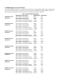
1
a
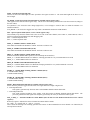
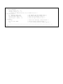
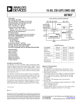
Application Note
Interfacing I2S-Compatible Audio Devices
To The ADSP-21065L Serial Ports
SDRAM
Host
Micro
a
a
2 Channel
D/A
2 Channel
D/A
ADSP 21065L
2 Channel
D/A
2 Channel
D/A
Version 1.0A
John Tomarakos
ADI DSP Applications
4/2/99
0. Introduction
The ADSP-21065L is the newest first generation SHARC member to be released, enabling 32-bit processing in either fixed or
floating point at a cost comparable to lower data word DSPs. This application note will cover the new features of the ADSP21065L Serial Ports, the addition of the I2S mode of operation, which allows a simple glueless interface to a wide range of
industry standard audio devices. The I2S format was developed and promoted by Philips Semiconductor, and today many
professional and consumer audio manufacturers use this standard interface for interconnection of audio devices, and as a result,
it has become the dominant, de-facto standard.
This document will serve as a reference for those who wish to understand the I2S serial protocol and the programming of the
ADSP-21065L to enable this mode of operation. First, a short tutorial will be given on the I2S bus, and then 21065L I2S mode
functionality will be described in detail. Finally, two I2S loopback examples will be demonstrated. One was written and tested
on the ADSP-21065L EZ-LAB with a simple wired loopback on the EMAFE interface, while the other example is an audio
loopback on the Bittware Research Systems Spinner Audio OEM Board, which uses 24-bit, 96 kHz I2S ADCs and DACs
(AKM semiconductor converters).
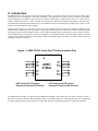
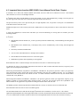
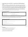
Figure 1. ADSP-21065L Serial Port I2S Interconnection Pins
a
RX0a
RX0b
RFS0
RCK0
RX1a
RX1b
RFS1
RCK1
ADSP21065L
• 4 RX Inputs with I2S support
• Supports 8 Input Audio Channels
TX0
TX0
a
TFS
b
T
0 CK0
TX1
TX1
a
TFS
b
T
1 CK1
• 4 TX Outputs with I2S support
• Supports 8 Output Audio Channels
The ADSP-21065L includes 2 on-chip serial ports –SPORT0 and SPORT1- that contain a new I2S mode of operation. Figure 1
shows the basic serial connections that enable this interface. The ADSP-21065L’s two serial ports provide 4 receive inputs and
4 transmit outputs to allow the processing of 8 I2S input audio channels and playback through 8 I2S output audio channels.
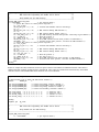
1. Philips I2S Serial Bus Protocol Overview
In consumer and professional audio products of recent years, the analog or digital f‘ront-end’of the DSP uses a digital audio
serial protocol known as I2S. Audio interfaces between various ICs in the past was hampered because each manufacturer had
dedicated audio interfaces that made it extremely difficult to interface these devices to each other. Standardization of audio
interfaces was promoted by Philips with the development of the Inter-IC-Sound (I2S) bus, a serial interface developed for
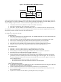
digital audio to enable easy connectivity and ensure successful designs. In short, I2S is a popular 3 wire serial bus standard
protocol developed by Philips for transmission of 2 channel (stereo) Pulse Code Modulation digital data, where each audio
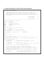
sample is sent MSB first. I2S signals, shown in Figures 1 and 2, consist of a bit-clock, Left/Right Clock (also is often referred to
as the Word Select) and alternating left and right channel data. This protocol can be compared to synchronous serial ports in
TDM mode with 2 timeslots (or channels) active. This multiplexed protocol requires only 1 data path to send/receive 2
channels of digital audio information.
Figure 1
I 2 S Digital Audio Serial Bus Interface Examples
Transmitter
Reciever
SCLK
LR_Select
DSP
Serial Bus Master
SDATA
Audio
D/A
Figure 2. Example I2S Timing Diagram for 16-bit
Stereo PCM Audio Data
SCLK
Left/Right
FS Clock
Left Channel Select
Right Channel Select
1 Serial Bit
Clock Delay
From LRCLK
transistion
Transmitter
Reciever
SCLK
Audio
A/D
LR_Select
Serial Data
0
15 14 13 12 11 10 9
M
S
B
8
7
6
5
Left Sample
4
3
2
1
0 15 14 13 12 11 10 9
L M
SS
BB
8
7
6
5
4
3
2
1
Right Sample
0
L
S
B
DSP
SDATA
Serial Bus Master
Audio data word sizes supported by various audio converter manufacturers range can be either
16, 18, 20, or 24 bits
2
As a result, today many analog and digital audio 'front-end' devices support the I S protocol. Some of these devices include:
•
•
•
•
•
•
Audio A/D and D/A converters
PC Multimedia Audio Controllers
Digital Audio Transmitters and Receivers that support serial digital audio transmission standards such as
AES/EBU, SP/DIF, IEC958, CP-340 and CP-1201.
Digital Audio Signal Processors
Dedicated Digital Filter Chips
Sample Rate Converters
The ADSP-21065L has 4 transmit and receive data pins (DT0A, DT0B, DT1A, DT1B), providing I2S serial port support for
interfacing to up to 8 commercially available I2S stereo devices, yielding 16 channels of audio with only 2 serial ports. The
ADSP-21065L's built-in support for the I2S protocol eliminates the need for interface logic with a FPGA and result in a simple,
glueless interface.
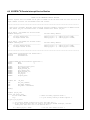
In addition to the master/slave timing generation of the word select and serial clock signals, it is also possible to generates the
clocks with an external controller or another audio device, which in effect makes both I2S devices slaves. An example of this is
shown in Figure 3. So for multiple devices, it is possible to synchronize all samples being transmitted or received with both
SPORTs through a common clock and word select signal.
2
Figure 3. I S Digital Audio Serial Bus Master Controller
Word Select and
Serial Clock
Controller
Transmitter
Receiver
SCLK
DSP
LR_Select
SDATA
Audio
D/A
Controller = Serial Bus
So this serial format efficiently transfers two-channel audio data for each I2S interconnection, while other control, status, and
sub-coding signals (for example, AES/EBU devices used in ADAT equipment and SP/DIF devices found in DVD players) are
transferred through a separate interface. As shown in the above figures, the buses three lines are:
•
•
•
Continuous serial clock - SCK (RCLKx or TCLKx if the 21065L is the master)
Word Select –WS (RFSx or TFSx if the 21065L is the master)
Serial Data - SD ( DTx, DRx on the 21065L SPORTs), this is in a 2-channel time-division multiplexed format
The transmitter, receiver or and system clock controller generates the serial clock and word select signals. Thus the I2S device
that generates the serial clock and word select is the master I2S device.
The Philips I2S bus defines the following:
Serial Data Pins:
• Serial data is transmitted in two’s complement format, with the MSB transmitted first, because the transmitter and
receiver may have different word lengths.
• The receiver ignores extra bits from the transmitter if greater than it’s capable (or programmed) serial length.
• If the receiver’s word length is greater than the data sent, all missing bits are set to zero internally
• The transmitter always sends the MSB of the next word one clock period after the WS changes.
• Serial data sent by the Transmitter can be sync’ed with either the trailing or leading edge of the SCLK.
• The Receiver (or the device in Slave Mode) always latches data on the leading edge of SCLK.
Word Select Pins:
• When WS = 0 or l‘ow’, the data is Channel 1, or Left Channel data in a stereo system.
• When WS = 0 or l‘ow’, the data is Channel 2, or Right Channel data in a stereo system.
• WS may change on a trailing or leading edge of the SCLK, but it does not need to be symmetrical.
• WS changes state one SCLK period before the MSB is transmitted.
• In slave mode, the data is latched on the leading edge of the serial clock signal.
• The slave determines synchronous timing of the serial data that will be transmitted, based on the external clock
generated by the master. The WS signal is latched on the leading edge of the clock signal. The slave takes into
account the propagation delays between the master clock and the data and/or word select signals. Thus, the total
delay is simply the sum of
- The delay between the master clock and the slave’s internal clock
- The delay between the internal clock and the data and/or the word select signals.
2
Other I S Specification Notes:
• To allow data to be clocked out on a falling edge, the delay is specified with respect to the rising edge of the clock
signal, always giving the reciever sufficient setup time.
• The data setup and hold time must not be less than the specified reciever set-up and hold time.
• In slave mode, the transmitter and receiver meed a clock signal with minimum HIGH and LOW periods so that
they can detect the signal.
• Any device can act as the serial bus master by providing the necessary clock signals.
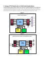
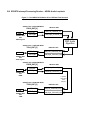
2. Usage of I2S Peripherals in 32-bit Audio Applications
The following Figures 4 and 5 show how the ADSP-21065L can be used in certain audio applications to take advantage of it’s
I2S mode for processing multiple channels of audio. One example shows a surround sound application, where multiple DACs
are required for the playback and placement of 6 channels of audio. Notice that for each I2S link, we have two channels of
audio transmission from a stereo ADC or to a stereo DAC. The other example shows how the ADSP-21065L can be used in a
prosumer application such as a digital mixer or digital recorder. Inputs and outputs can be either analog or digital.
Figure 4.
Example Consumer Audio DSP System Using the ADSP-21065L
Home Theatre System
Left Front
Laserdisc
Player
I2S Link
a
ADSP21065L
2
Compact I S Link
Disk Player
Stereo
ADC
I2S Link
Stereo
ADC
I2S Link
I2S Link
Stereo
DAC
Right Front
I2S Link
Stereo
DAC
Left Rear
I2S Link
Stereo
DAC
Right Rear
I2S Link
SP/DIF
X-mitter
Center
Subwoofer
Addr.
Data
SRAM /
SDRAM
RCA
Connector
8, 6, or 32bit Host uP
Figure 5.
Example Prosumer Audio DSP System Using the ADSP-21065L
digital 4-track home studio recording/playback system
AES/EBU
reciever
I2S Link
a
ADSP21065L
2
Compact I S Link
Disk Player
Channel 1
Channel 2
Stereo
ADC
I2S Link
Channel 3
Channel 4
Stereo
ADC
I2S Link
Addr.
SRAM /
SDRAM
I2S Link
Stereo
DAC
I2S Link
Stereo
DAC
I2S Link
CD
Recorder
I2S Link
AES/EBU
X-mitter
Data
XLR
Connector
to DAT
machine
8, 6, or 32bit Host uP
Left
Right
3. Digital Audio Interface I2S Devices: SPD/IF & AES/EBU Digital
Audio Transmitters and Receivers
The ADSP-21065L's I2S interface easily allows transmission and reception of audio data using industry standard digital audio
serial protocols. These devices act as a 'digital' front-end for the DSP. There are primarily 2 dominant digital protocols used
today. One is used for professional audio and the other for consumer audio applications.
AES/EBU (Audio Engineering Society/European Broadcast Union)
AES/EBU is a standardized digital audio bit serial communications protocol for transmitting and receiving two channels of
digital audio information through a transmission line (balanced or unbalanced XRL microphone cables and audio coax cable
with RCA connectors). This format of transmission is used to transmit digital audio data over distances of 100 meters. Data
can be transmitted up to 24 bit resolution, along with control, status and sample rate information embedded in frame[37].
AES/EBU is considered to be the standard protocol for professional audio applications. It is a common interface that is used in
interfacing different professional mixing and DAT recording devices together. The AES3-1992 Standard can be obtained from
the Audio Engineering Society.
Figure 6. AES3 Frame Format
0
27 28 29 30 31
3 4
L
Preamble
S
B
M
Up to 24 bit Audio Sample Word S
(16/20/24 Data)
Audio Engineering Society Recommended Practice:
AES3-1992: Serial Transmission Format for TwoChannel Linearly Represented Digital Audio Data
V
U
C
P
B
V = Validity
U = User Data
C = Channel Status
P = Parity Bit
SPD/IF (Sony/Philips Digital Interface Format)
SPD/IF is based on the AES/EBU standard in operating in 'consumer' mode. The physical medium is an unbalanced RCA
cable. The consumer mode carries less control/status information. Typical applications where this interface can be found is in
home theater equipment (Dolby Digital & DTS Decoders) and CD players.
Digital Audio Receivers typically receive AES/EBU and SP/DIF information and convert the audio information into the I2S (or
parallel) format for the ADSP-21065L, as well as provide status information (through flag pins or a parallel interface) that is
received along with the audio data. Digital Audio Transmitters can take an I2S audio stream from the ADSP-21065L and
transmit the audio data along with control information in AES/EBU and SPD/IF formats. Control and status information
contains useful information such as the sampling rate of the data being transmitted or received.
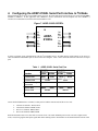
4. Configuring the ADSP-21065L Serial Port Interface In I2S Mode
When interfacing an I2S device to an ADSP-21065L processor, the interconnection between both devices can be through either
SPORT0 or SPORT1. In this application note, SPORT0 is used to demonstrate the I2S loopback test since SPORT1 is
activated for communications with the AD1819a SoundPort Codec.
Figure 7. ADSP-21065L SPORTs
a
RX0
RX0
a
R
b FS0
RCK0
RX1
RX1
a
R
b FS1
RCK1
ADSP21065L
TX0
TX0
a
T
b FS
TCK0
0
TX1
TX1
a
T
b FS
TCK1
1
In order to facilitate serial communications with an I2S-compatible device, the DSP designer would simply tie the device to
either the SPORT0 and SPORT1 pins as shown in the above diagram. Table 1 below shows the function of all of the serial port
pins:
Table 1. ADSP-21065L Serial Port Pins
Function
SPORT0
A Chn
B Chn
Transmit data
DT0A
Transmit clock
Receive cock
Receive frame sync
B Chn
DT1A
DT1B
TCLK0
TCLK1
TFS0
TFS1
Transmit frame sync/
word select
Receive data
DT0B
SPORT1
A Chn
DR0A
DR0B
DR1A
DR1B
RCLK0
RCLK1
RFS0
RFS1
Notice that both SPORTs have 2 channel, or data pins for both the transmit side and the receive side.
•
•
•
•
Transmit A Channels - DT0A, DT1A
Transmit B Channels –DT0B, DT1B
Receive A Channels –DR0A, DR1A
Receive B Channels –DR0B, DR1B
Both the transmitter and receiver have their own serial clocks. The TFSx and RFSx pins become word select signals in I2S
mode, versus being regular small pulse signals that initiate shifting of data. Both channel A and channel B share both the serial
clock and frame syncs. For example, DR0A and DR0B use the RCLK0 and RFS0 signals to receive data, regardless if they are
internally or externally generated.
Since there are 8 data pins (4 transmit and 4 receive channels), then for I2S mode of operation where two channels of data of
transmitted or received on each data pin, the actual number of channels is doubled. Therefore, both serial ports combined gives
the capability of passing up to 8 input channels of audio to the DSP and 8 output channels of audio, giving 16 audio streams
with both SPORTs.
4.1 I2S-related bits in the SPORT Transmit and Receive Control Registers
The ADSP-21065L has two transmit (STCTL0, STCLT1) and two receive (SRCTL0, SRCTL1) control registers for
configuring the timing signals, data size and DMA parameters. Figure 8 below highlights the related bits.
I2 S
Figure 8.
Control bits in the SPORT Control Registers
l I2S enable
l Sport channel enable (SPEN_x)
l Word length (SLEN)
l I2S channel transfer order (L_FIRST)
l Frame sync (word select) generation
l Master mode enable
l DMA channel enable (SDEN_x)
l DMA chaining enable (SCHEN_x)
OPMODE – Operation Mode (bit 11)
Setting this bit to a 1 will enable I2S mode, versus standard mode when it is 0.
MSTR – Master/Slave Mode Enable (bit 10)
When this bit is set to a 1 in the SPORT transmit control register, then the transmitter is the master. When it is cleared, the
transmitter is the slave
When this bit is set to a 1 in the SPORT receive control register, then the receiver is the master. When it is cleared, the receiver
is the slave
For Master Mode, the frame sync/word select and serial clock is internally generated, and values must be specified in the
transmit or receive divisor registers.
For Slave Mode, the frame sync/word select and serial clock is externally generated, and any values specified in the divisor
registers are ignored.
For I2S master mode only in revs 0.2 and prior, otherwise it is applicable for master and slave parts of revision 0.3 and greater.
With this bit set, the master transmitter sends the left channel first and the master receiver shifts in the right channel first. The
L_FIRST control bit is ignored for slave mode (refer to anomaly list). With these earlier revisions, there is no way to select if
the first transmitted or received word at startup will align to the left or right I2S channel, unless the WS pin is connected to a
flag input pin for detection at the enabling of the SPORT.
SLEN – Data Word Length (bits 4-8)
This bit sets the serial word length, the value specified in the register is S
‘ LEN –1’. The serial data length can be from 3 to 32
bits in length.
FS_BOTH – Frame Sync Word Generation (bit 22, transmit control registers only)
(This applies for the transmit control register only). This bit select when during transmission to issue the word select (change in
the state of WS)
If FS_BOTH= 0, the word select state change (high t–o-low, or low-to-high) is issued if data is in either the transmit A or
transmit B channel.
If FS_BOTH= 1, the word select toggles state only if data is in BOTH the transmit A and B channels.
SPL – Sport Loopback Mode (bit 22, receive control registers only)
This internally loops back the transmit side to the receive side of the same channel (TX A to RX A, TX B to RX B). This is
useful for running internal SPORT tests and debugging code.
SPL = 0, disables loopback mode.
SPL = 1, enables loopback mode.
SPEN_A – SPORT Channel A Enable (bit 0)
This enables and disables the SPORT’s A channel. Performs a software reset.
SPEN_B – SPORT Channel B Enable (bit 24)
This enables and disables the SPORT’s B channel. Performs a software reset.
SDEN_A – SPORT Channel A DMA Enable (bit 18)
Enables and disables SPORT DMA operation (versus interrupt driven transfers)
SDEN_A = 0, disables DMA transfers for channel A, interrupt generated for every word transmitted or received
SDEN_A = 1, enables DMA transfers for channel A
SDEN_B - SPORT Channel B DMA Enable (bit 20)
SDEN_B = 0, disables DMA transfers for channel B, interrupt generated for every word transmitted or received
SDEN_B = 1, enables DMA transfers for channel B
SCHEN_A – SPORT DMA Chaining Channel A Enable (bit 19)
0= Disables DMA chaining
1=Enables DMA chaining
SCHEN_B – SPORT DMA Chaining Channel B Enable (bit 21)
0= Disables DMA chaining
1=Enables DMA chaining
DITFS – Data Independent TFS (bit 15, transmit control registers only)
Selects when the processor toggles the TFS word select signal from low-to-high or high-to-low
0 = Data dependent TFS
TFS signal is generated only when nes data is in the SPORT chennel’s transmit data buffer.
1 = Data independent TFS
TFS signal generated regardless of the validity of the data present in SPORT channel’s transmit data buffer. The
processor generates the TFS signal at the frequency specified by the value you load in the TDIV register.
TXS_A, RXS_A - Transmit and Receive Status Buffers (bits 30 and 31 in the SPORT transmit and receive control
registers)
Read-only registers. Indicates the status of channel A’s transmit buffer contents
00 = empty, 10 = partially full, 11 = full, 01 = reserved.
This is useful in detecting if the interrupt generated was because of data transmitted/received in channel A or channel B (for
interrupt driven transfers.
4.2 States of SPORT Pins When Operating in Master or Slave Mode
The following tables 2 through 5 show the states of the pins on both SPORT0 and SPORT1 when the 21065L is set up for
either master mode or slave mode. The states of the pins are shown for either a transmitter or reciever. The particular pins are
matched up with the pins of the connecting I2S device (in the second column), showing generic definitions for the I2S
compatible device, which contains a serial clock, word select, and serial data signals. The states of these pins, which are either
outputs or inputs, are indicated in the third column in the tables.
Table 2. 21065L I2S Receiver in Master Mode
ADSP-2106x Pin:
I2S Device Pin:
Driven By:
RCLK0, RCLK1
SCLK
21065L
RFS0, RFS1
WS (Word Select)
21065L
DR0A, DR0B, DR1A, DR1B
SD (Serial Data Out)
I2S device
Table 3. 21065L I2S Receiver in Slave Mode
ADSP-2106x Pin:
I2S Device Pin:
Driven By:
RCLK0, RCLK1
SCLK
I2S device
RFS0, RFS1
WS (Word Select)
I2S device
DR0A, DR0B, DR1A, DR1B
SD (Serial Data Out)
I2S device
Table 4. 21065L I2S Transmitter in Master Mode
ADSP-2106x Pin:
I2S Device Pin:
Driven By:
TCLK0, TCLK1
SCLK
21065L
TFS0, TFS1
WS
21065L
DT0A, DT0B, DT1A, DT1B
SD (Serial Data In)
21065L
Table 5. 21065L I2S Transmitter in Slave Mode
ADSP-2106x Pin:
I2S Device Pin:
Driven By:
TCLK0, TCLK1
SCLK
I2S device
TFS0, TFS1
WS
I2S device
DT0A, DT0B, DT1A, DT1B
SD (Serial Data In)
21065L
4.3 Important Notes from the ADSP-21065L User’s Manual ‘Serial Ports’ Chapter
In I2S Mode, one or both of the transmit channels can transmit, and one or both receive channels can receive. Each channel
either transmits or receives Left and Right Channels.
In I2S Mode, when both A and B channels are used, they transmit or receive data simultaneously, sending or receiving bit 0 on
the same edge of the serial clock, bit 1 on the next edge of the serial clock, and so on.
The processor always drives, never puts the DT pins in a high impedance state, except when a serial port is in multichannel
mode and an inactive time slot occurs.
SPORT interrupts occur on the second system clock (CLKIN) after the serial port latches or drives out the last bit of the serial
word.
A serial port configured for external clock and frame sync can start transmitting or receiving data two CLKIN cycles after
becoming enabled.
In I2S mode:
•
Both SPORTs transmit channels (Tx_A and Tx_B) always transmit simultaneously, each transmitting left and right I2S
channels.
•
Both SPORT receive channels (Rx_A and Rx_B) always receive simultaneously, each receiving left and right I2S
channels.
•
Data always transmits in MSB format.
•
You can select either DMA-driven or interrupt-driven transfers.
•
TFS and RFS are the transmit and receive word select signals
•
Multichannel operation and companding are not supported.
Both transmitters share a common interrupt vector and both receivers share a common interrupt vector.
To determine the source of an interrupt, applications must check the TXSx or RXSx data buffer status bits, respectively (this
applies only for interrupt driven transfers).
When using both transmitters (FS_BOTH=1) and MSTR=1 and DITFS=0, the processor generates a frame sync signal only
when both transmit buffers contain data because both transmitters share the same CLKDIV and TFS. So, for continuous
transmission, both transmit buffers must contain new data. To enable continuous transmission when only one transmit buffer
contains data, set FS_BOTH=0.
When using both transmitters and MSTR=1 and DITFS=1, the processor generates a frame sync signal at the frequency set by
FSDIV=x whether or not the transmit buffers contain new data. In this case, the processor ignores the FS_BOTH bit. The
DMA controller or the application is responsible for filling the transmit buffers with new data.
The SPORT generates and interrupt when the transmit buffer has a vacancy or whenever the receive buffer has data.
Each transmitter and receiver has it’s own set of DMA registers.
The same DMA channel drives both the left and right I2S channels for the transmitter or for the receiver. The software
application must demultiplex the left and right channel data received by the RX buffer (this means that when data is transferred
to a receive DMA buffer, the data is interleaved where the left and right data alternate in consecutive locations in memory).
4.4 SPORT DMA Channels and Interrupt Vectors
There are 8 dedicated DMA channels for the I2S channel A and B buffers on both SPORT0 and SPORT1. The IOP addresses
for the DMA registers are shown in the table below for each corresponding channel and SPORT data buffer.
Table 6. 8 SPORT DMA channels and data buffers
Chn Data Buffer Address
Description
0
Rx0A
0x0060 0x0064
Serial port 0 receive; A data
1
Rx0B
0x0030 0x0034
Serial port 0 receive; B data
2
Rx1A
0x0068 0x006C
Serial port 1 receive; A data
3
Rx1B
0x0038 0x003C
Serial port 1 receive; B data
4
Tx0A
0x0070 0x0074
Serial port 0 transmit; A data
5
Tx0B
0x0050 0x0054
Serial port 0 transmit; B data
6
Tx1A
0x0078 0x005C
Serial port 1 transmit; B data
7
Tx1B
0x0058 0x005C
Serial port 1 transmit; B data
Each serial port has a transmit DMA interrupt and a receive DMA interrupt (shown in Table 7 below). With serial port DMA
disabled, interrupts occur on a word by word basis, when one word is transmitted or received. Table 7 also shows the interrupt
priority, because of their relative location to one another in the interrupt vector table. The lower the interrupt vector address, the
higher priority interrupt. Note that channels A and B for the transmit and receive side of each SPORT share the same interrupt
location. Thus, data for both DMA buffers is processed at the same time, or on a conditional basis depending on the state of the
buffer status bits in the SPORT control registers.
Table 7. ADSP-21065L Serial Port Interrupts
Priority
Interrupt1 Function
SPR0I
SPORT0 receive DMA channels 0 and 1
SPR1I
SPORT1 receive DMA channels 2 and 3
SPT0I
SPORT0 transmit DMA channels 4 and 5
SPT1I
SPORT1 transmit DMA channels 6 and 7
EP0I
Ext. port buffer 0 DMA channel 8
EP1II
Ext. port buffer 1 DMA channel 9
1
Interrupt names are defined in the def21065.h include file supplied
with the ADSP-21000 Family Visual DSP Development Software.
Highest
Lowest
4.5 Serial Port Related IOP Registers
This section briefly highlights the list of available SPORT-related IOP registers that you will need to program when configuring
the SPORTs for I2S mode. To program these registers, you write to the appropriate address in memory using the symbolic
macro definitions supplied in the def21065l.h file (included with the Visual DSP tools in the /INCLUDE/ directory).
External devices such as another 21065L, or a host processor, can write and read the SPORT control registers to set up a serial
port DMA operation or to enable a particular SPORT. These registers are shown in the table below. The SPORT DMA IOP
registers are covered in section 4.8. As we will see in the next section, only a few of the available registers shown below need
to be programmed to set up I2S mode. These registers are highlighted in bold text.
Table 8. Serial Port IOP Registers
Register
STCTL0
SRCTL0
TDIV0
RDIV0
MTCS0
MRCS0
MTCCS0
MRCCS0
KEYWD0
IMASK0
IOP Address
0xe0
0xe1
0xe4
0xe6
0xe8
0xe9
0xea
0xeb
0xec
0xed
Description
SPORT0 transmit control register
SPORT0 receive control register
SPORT0 transmit divisor
SPORT0 receive divisor
SPORT0 multichannel transmit select
SPORT0 multichannel receive select
SPORT0 multichannel transmit compand select
SPORT0 multichannel receive compand select
SPORT0 receive comparison register
SPORT0 receive comparison mask register
SPORT1
STCTL1
SRCTL1
TDIV1
RDIV1
MTCS1
MRCS1
MTCCS1
MRCCS1
KEYWD1
IMASK1
0xf0
0xf1
0xf4
0xf6
0xf8
0xf9
0xfa
0xfb
0xfc
0xfd
SPORT1 transmit control register
SPORT1 receive control register
SPORT1 transmit divisor
SPORT1 receive divisor
SPORT1 multichannel transmit select
SPORT1 multichannel receive select
SPORT1 multichannel transmit compand select
SPORT1 multichannel receive compand select
SPORT1 receive comparison register
SPORT1 receive comparison mask register
SPORT
Data
Buffers
TX0_A
RX0_A
TX1_A
RX1_A
TX0_B
RX0_B
TX1_B
RX1_B
0xe2
0xe3
0xf2
0xf3
0xee
0xef
0xfe
0xff
SPORT0 transmit data buffer, channel A data
SPORT0 receive data buffer, channel A data
SPORT1 transmit data buffer, channel A data
SPORT1 receive data buffer, channel A data
SPORT0 transmit data buffer, channel B data
SPORT0 receive data buffer, channel B data
SPORT1 transmit data buffer, channel B data
SPORT1 receive data buffer, channel B data
SPORT0
4.6 SPORT0 I2S Mode IOP Register Configuration For 21065L EZ-LAB Loopback Test
The configuration for SPORT0 for the first example in the Appendix A is set up as follows:
•
•
•
•
•
•
•
32-bit serial word length
Enable SPORT0 transmit and receive DMA functionality
Enable DMA chaining functionality for SPORT0 transmit and receive
Internal TX Serial Clock (TCLK0) - the SPORT0 I2S transmitter provides the serial clock to the 65L’s SPORT0 receiver.
Internal TFS0, thus the SPORT0 channel A transmitter is the I2S master.
External RX Serial Clock (RCLK0) and Word Select (RFS0), thus the receiver Channel A port is the slave.
Transmit and Receive DMA chaining enabled. The dsp program declares 2 buffers - i2s_tx_buf [2] and i2s_rx_buf[2] for DMA transfers of SPORT0 I2S transmit and receive stereo data on Channel A.
.var i2s_rx_buf[STEREO_LR];
/* stereo I2S receive buffer */
.var i2s_tx_buf[STEREO_LR];
/* stereo I2S transmit buffer */
Program_I2Smode_SPORT0_Registers:
/* sport0 receive control register */
R0 = 0x000D09F1;
/* slave mode, slen = 32 , sden_A & schen_A enabled */
dm(SRCTL0) = R0;
/* sport 0 receive control register */
/* sport0 transmit control register */
R0 = 0x000D0DF1;
/* master mode, data depend, slen = 32, sden_A & schen_A enabled */
dm(STCTL0) = R0;
/* sport 0 transmit control register */
•
The ADSP-2165L provides an internally generated 96 kHz frame sync (TFS0). It must be a 96 kHz frame rate since the
AC97 specified frame rate of the AD1819 is 48 kHz, and we get a left and right sample per 48 KHz frame from the
AD1819A. Thus, the word select rate is twice as fast as the AD1819a AC-link frame rate in order to send or receive 2 I2S
samples per AC97 audio frame.
/* sport0 I2S word select (transmit frame sync) divide register
We want to set up a frame sync of 96KHz, since this is twice of 48 KHz
Data coming from the AD1819a is 48 KHz, so to send both left and right data via the
I2S ports, we need to send the stereo data at a rate = 2x of the AD1819a Fs. The TFS will
toggle every 96 K, but both left and right I2S data is being transmitted at a rate of 48K
equivalent to the AD1819a frame rate.
The SPORT0 ISR will be called at a rate of 48K since the I2S DMA buffers are 2 words deep.
*/
R0 = 0x007C0004;
/* TCLKDIV=[2xfCLKIN(60MHz)/SCLKfreq(12MHz)]-1 = 0x0004 */
dm(TDIV0) = R0;
/* TFSDIV=[TCLKfrq(12 MHz)/TFSfrq(96.0K)]-1 = 124 = 0x007C */
/* sport0 receive frame sync divide register */
R0 = 0x00FF0000;
/* SCKfrq(12.288M)/RFSfrq(48.0K)-1 = 0x00FF */
dm(RDIV0) = R0;
•
No companding.
/* sport0 transmit and receive multichannel companding enable registers */
R0 = 0x00000000;
/* no companding */
dm(MRCCS0) = R0;
/* no companding on receive */
dm(MTCCS0) = R0;
/* no companding on transmit */
•
Multichannel Mode Disabled
/* sport0 receive and transmit multichannel word enable registers */
R0 = 0x00000000;
/* enable transmit and receive channels 0-8 */
dm(MRCS0) = R0;
dm(MTCS0) = R0;
4.7 SPORT0 I2S Mode IOP Register Configuration For Interfacing to 2 (24-bit, 96 kHz)
Stereo ADCs and DACs:
The configuration for SPORT0 for the second example in the Appendix A is set up as follows:
•
•
•
•
•
24-bit serial word length
Enable SPORT0 transmit and receive DMA functionality on Channels A & B
Enable DMA chaining functionality for SPORT0 transmit and receive on Channels A & B
Slave Mode for the I2S channel A & B transmitters and receivers.
• External TX Serial Clock (TCLK0) - the SPORT0 I2S transmit clock for Channels A & B is externally generated
• External TFS0, thus the SPORT0 channel A and B transmitters are the I2S slave devices.
• External RX Serial Clock (RCLK0) and Word Select (RFS0), thus the receiver Channel A port is the slave.
Transmit and Receive DMA chaining enabled. The dsp program declares 4 DMA buffers –tx0a_buf[2], tx0b_buf[2],
rx0a_buf[2], rx0b_buf[2] - for DMA transfers of SPORT0 transmit and receive serial (stereo left/right) data on channels
A & B.
#define
STEREO_LR
2
.var rx0a_buf[STEREO_LR];
.var rx0b_buf[STEREO_LR];
.var tx0a_buf[STEREO_LR];
.var tx0b_buf[STEREO_LR];
/*
/*
/*
/*
stereo
stereo
stereo
stereo
I2S
I2S
I2S
I2S
primary receive a buffer */
secondary receive b buffer */
primary transmit a buffer */
secondary transmit b buffer */
Program_I2Smode_SPORT0_Registers:
/* sport0 receive control register */
R0 = 0x013C0971; /* slave mode,slen = 24,sden_A & schen_A & sden_B & schen_B enabled */
dm(SRCTL0) = R0; /* sport 0 receive control register */
/* sport0 transmit control register */
R0 = 0x017C8971; /* slave mode,slen = 24,sden_A & schen_A & sden_B & schen_B enabled */
dm(STCTL0) = R0; /* sport 0 transmit control register */
•
The ADSP-21065L transmitter and receiver A and B channels accept an externally generated 96 kHz serial clock (RCLK0
and TCLK0)frame sync (TFS0 and RFS0). Therefore, the divisor registers are set to zero.
/* sport0 I2S word select (transmit frame sync) divide register */
R0 = 0x00000000;
/* TCLKDIV=[2xfCLKIN(60MHz)/SCLKfreq(12MHz)]-1 */
dm(TDIV0) = R0;
/* TFSDIV=[TCLKfrq(12 MHz)/TFSfrq(96.0K)]-1 */
/* sport0 I2S receive word select divide register */
R0 = 0x00000000;
dm(RDIV0) = R0;
•
Multichannel Mode Disabled
/* sport0 receive and transmit multichannel word enable registers */
R0 = 0x00000000;
/* multichannel mode disabled */
dm(MRCS0) = R0;
dm(MTCS0) = R0;
•
No companding.
/* sport0 transmit and receive multichannel companding enable registers */
R0 = 0x00000000;
/* no companding */
dm(MRCCS0) = R0;
/* no companding on receive */
dm(MTCCS0) = R0;
/* no companding on transmit */
4.8 DMA Registers for the I2S Ports
The following register descriptions are provided in the defs21065l.h file for programming the DMA registers associated with
the I/O processor’s DMA controller. We will look at how these registers are programmed for DMA chaining, in which the
DMA registers are reinitialized automatically whenever a serial port interrupt request is generated.
Table 9. SPORT DMA IOP Registers
DMA Register Description
DMA Register
DMA Channel 0 Index Register
IIR0A
DMA Channel 0 Modify Register
IMR0A
DMA Channel 0 Count Register
CR0A
DMA Channel 0 Chain Pointer Register
CPR0A
DMA Channel 0 General Purpose Register GPR0A
IOP Address
0x60
0x61
0x62
0x63
0x64
SPORT0 Receive
Channel B
DMA Channel 1 Index Register
DMA Channel 1 Modify Register
DMA Channel 1 Count Register
DMA Channel 1 Chain Pointer Register
DMA Channel 1 General Purpose Register
IIR0B
IMR0B
CR0B
CPR0B
GPR0B
0x30
0x31
0x32
0x33
0x34
SPORT1 Receive
Channel A
DMA Channel 2 Index Register
DMA Channel 2 Modify Register
DMA Channel 2 Count Register
DMA Channel 2 Chain Pointer Register
DMA Channel 2 General Purpose Register
IIR1A
IMR1A
CR1A
CPR1A
GPR1A
0x68
0x69
0x6A
0x6B
0x6C
SPORT1 Receive
Channel B
DMA Channel 3 Index Register
DMA Channel 3 Modify Register
DMA Channel 3 Count Register
DMA Channel 3 Chain Pointer Register
DMA Channel 3 General Purpose Register
IIR1B
IMR1B
CR1B
CPR1B
GPR1B
0x38
0x39
0x3A
0x3B
0x3C
SPORT0 Transmit
Channel A
DMA Channel 4 Index Register
DMA Channel 4 Modify Register
DMA Channel 4 Count Register
DMA Channel 4 Chain Pointer Register
DMA Channel 4 General Purpose Register
IIT0A
IMT0A
CT0A
CPT0A
GPT0A
0x70
0x71
0x72
0x73
0x74
SPORT0 Transmit
Channel B
DMA Channel 5 Index Register
DMA Channel 5 Modify Register
DMA Channel 5 Count Register
DMA Channel 5 Chain Pointer Register
DMA Channel 5 General Purpose Register
IIT0B
IMT0B
CT0B
CPT0B
GPT0B
0x50
0x51
0x52
0x53
0x54
SPORT1 Transmit
Channel A
DMA Channel 6 Index Register
DMA Channel 6 Modify Register
DMA Channel 6 Count Register
DMA Channel 6 Chain Pointer Register
DMA Channel 6 General Purpose Register
IIT1A
IMT1A
CT1A
CPT1A
GPT1A
0x78
0x79
0x7A
0x7B
0x7C
SPORT1 Transmit
Channel B
DMA Channel 7 Index Register
DMA Channel 7 Modify Register
DMA Channel 7 Count Register
DMA Channel 7 Chain Pointer Register
DMA Channel 7 General Purpose Register
IIT1B
IMT1B
CT1B
CPT1B
GPT1B
0x58
0x59
0x5A
0x5B
0x5C
SPORT0 Receive
Channel A
4.9 Setting Up the 21065L DMA Controller for Chained SPORT DMA Transfers
To transmit and receive digital audio data to/from an I2 S device, one efficient method is to use serial port DMA Chaining to
transfer data between the I2 S serial bus and the DSP core. There are obvious benefits for doing this. First of all, DMA
transfers allow efficient transfer of data between the serial port circuitry and DSP internal memory with zero-overhead, i.e.
there is no processor intervention of the SHARC core to manually transfer the data. Secondly, there is a one-to-one
correspondence of the location of the left and right I2 S data in the transmit and receive SPORT DMA buffer locations with
the actual I2S audio channel on the serial bus. Thirdly, an entire block of I2 S audio data can be transmitted or received
before generating a single interrupt. In our example, the DMA buffer is only two words deep, so that an interrupt is generated
whenever a left sample and a right sample is transmitted or received. However, the user can further reduce interrupt overhead
by making the DMA buffer size larger, as long as it is by a factor of two so that data is always interleaved and aligned
properly. Thus, this method of serial port processing is more efficient for the SHARC core to process data, versus interrupt
driven transfers which would occur more frequently. Using chained DMA transfers allows the ADSP-21065L DMA
controller to autoinitialize itself between multiple DMA transfers. When the entire contents of the current SPORT buffers
have been received or transmitted, the ADSP-21065L will automatically set up another serial port DMA transfer to repeated
again. For further information on DMA chaining, the reader can refer to page 6-39 in the ADSP-21065L User's Manual
The chain pointer register (CPxxx) is used to point to the next set of TX and RX buffer parameters stored in memory. For
example, SPORT0 channel A DMA transfers are initiated by writing the DMA buffer's memory address to the CPR0A
register for SPORT0 A receive and CPT0A register for SPORT0 A transmit. The transmit and receive SCHEN_A and
SCHEN_B bits in the SPORTx Control registers enable DMA chaining.
To autoinitialize repetitive DMA-chained transfers, the programmer needs to set up a buffer in memory called a Transfer
Control Block (TCB) that will be used to initialize and further continue the chained DMA process. Transfer Control Blocks
are locations in Internal Memory that store DMA register information in a specified order. Figure 9 below demonstrates
defined TCBs in internal memory for SPORT0 Channel A. The Chain Pointer Register (CPR0A and CPT0A) stores the
location of the next set of TCB parameters to be automatically be downloaded by the DMA controller at the completion of the
DMA transfer, which in this case it points back to itself.
Figure 9. TCBs for Chained DMA Transfers
of SPORT0 Channel A Receive and Transmit
rcv0a_tcb[8]
xmit0a_tcb[8]
DM(rcv0a_tcb + 0)
ECEPx (not used
with SPORTs)
DM(xmit0a_tcb + 0)
DM(rcv0a_tcb + 1)
EMEPx (not used
with SPORTs)
DM(xmit0a_tcb + 0)
DM(rcv0a_tcb + 2)
EIEPx (not used
with SPORTs)
DM(xmit0a_tcb + 0)
DM(rcv0a_tcb + 3)
GPR0A
DM(xmit0a_tcb + 0)
GPT0A
DM(rcv0a_tcb + 4)
CPR0A
DM(xmit0a_tcb + 0)
CPT0A
DM(rcv0a_tcb + 5)
CR0A
DM(xmit0a_tcb + 0)
CT0A
DM(rcv0a_tcb + 6)
IMR0A
DM(xmit0a_tcb + 0)
IMT0A
DM(rcv0a_tcb + 7)
IIR0A
DM(xmit0a_tcb + 0)
IIT0A
These TCBs for both the transmit and receive buffers can be defined in the variable declaration section of the DSP assembly or
C code. In the I2 S example code shown in appendix A, the TCBs for SPORT0 channel A are defined as follows:
.var I2s_rcv_tcb[8] = 0, 0, 0, 0, 0, 2, 1, 0;
.var I2s_xmit_tcb[8] = 0, 0, 0, 0, 0, 2, 1, 0;
/* receive tcb */
/* transmit tcb */
Note that the DMA count and modify values can be initialized in the buffer declaration so that they are resident after a DSP
reset and boot. However, at runtime, further modification of the buffer is required to initiate the DMA autobuffer process.
To setup and initiate a chain of SPORT DMA operations at runtime, the 21065L should follow this sequence:
1.
Set up SPORT transmit and Receive TCBs (transfer control blocks). The TCBs are defined in the data variable
declaration section of your code. Before setting up the values in the TCB and kicking off the DMA process, make sure the
SPORT registers are programmed along with the appropriate chaining bits required in step 2.
2.
Write to the SPORT0 transmit and receive control registers (STCTL0 and STCRL0), setting the SDEN_A and/or
SDEN_B enable bit to 1 and the SCHEN_A and/or SCHEN_B chaining enable bit to a 1.
3.
Write the internal memory index address register (IIxxx) of the first TCB to the CPxxx register to start the chain. The
order should be as follows:
a) write the starting address of the SPORT DMA buffer to the TCBs internal index register IIxxx location (TCB
buffer base address + 7). You need to get the starting address of the defined DMA buffer at runtime and copy it
into this location in the TCB.
b) write the DMA internal modify register value IMxxx to the TCB (TCB buffer base address + 6). Note that this
step may be skipped if it the location in the buffer was initialized in the variable declaration section of your code.
c) write the DMA internal count register Cxxx value to the TCB (TCB buffer base address + 5). Also note that
this step may be skipped if it the location in the buffer was initialized in the variable declaration section of your
code.
d) get the IIxxx value of the TCB buffer that was previously stored in step (a), set the PCI bit with a that internal
address value, and write the modifed value to the chain pointer location in the TCB (TCB buffer base offset +
4).
e) write the same ‘PCI-bit-set’ internal address value from step (d) manually into that DMA channels chain pointer
register (CPxxx). At this moment the DMA chaining begins (If the SPORT enable bit was already set,
otherwise transfers will not begin until the SPORT enable bit is set.
The DMA interrupt request occurs whenever the Internal Count Register Cxxx decrements to zero.
SPORT DMA chaining occurs independently for the transmit and receive channels of the serial port. After the SPORT0
receive buffer is filled with new data, a SPORT0 receive interrupt is generated, and the data placed in the receive buffer is
available for processing. The DMA controller will autoinitialize itself with the parameters set in the TCB buffer and begin to
refill the receive DMA buffer with new data in the next audio frame. In our loopback example, the processed data is then
placed in the SPORT transmit buffer, where it will then be DMA’ed out from memory to the SPORT DT0A pin. After the
entire buffer is transmitted from internal memory to the SPORT circuitry, the DMA controller will autoinitialize itself with the
stored TCB parameters to perform another DMA transfer of new data that will be placed in the same transmit buffer.
Below are example assembly instructions used to set up the Transfer Control Blocks for SPORT0 Channel A in the 21065L
EZ-LAB example shown in appendix A. These values are reloaded from internal memory to the DMA controller after the
entire SPORT DMA buffer has been received or transmitted. If you want to reduce interrupt overhead, these buffers can be
made a multiple of 2 which would increase the buffer size. Data is interleaved in memory with the left sample first, followed
by the right sample, then the left again, and so on…
.segment /dm
dm_I2S;
/* define buffer size to match I2S TDM stereo channels */
#define
STEREO_LR
2
.var I2s_rx_buf[STEREO_LR];
.var I2s_tx_buf[STEREO_LR];
/* stereo I2S receive buffer */
/* stereo I2S transmit buffer */
.var I2s_rcv_tcb[8] = 0, 0, 0, 0, 0, 2, 1, 0;
.var I2s_xmit_tcb[8] = 0, 0, 0, 0, 0, 2, 1, 0;
.endseg;
/* receive tcb */
/* transmit tcb */
.segment /pm
pm_code;
/*-------------------------------------------------------------------------------- */
/*
DMA Controller Programming For SPORT0 I2S Tx and Rx
*/
/*
*/
/*
Setup SPORT0 I2S for DMA Chaining:
*/
/*-------------------------------------------------------------------------------- */
Program_DMA_Controller_SPT0:
r1 = 0x0001FFFF;
/* cpx register mask */
/* sport0 dma control tx chain pointer register */
r0 = I2s_tx_buf;
dm(I2s_xmit_tcb + 7) = r0;
/* internal dma address used for chaining*/
r0 = 1;
dm(I2s_xmit_tcb + 6) = r0;
/* DMA internal memory DMA modifier */
r0 = 2;
dm(I2s_xmit_tcb + 5) = r0;
/* DMA internal memory buffer count */
r0 = I2s_xmit_tcb + 7;
/* get DMA chaining internal mem pointer containing tx_buf address */
r0 = r1 AND r0;
/* mask the pointer */
r0 = BSET r0 BY 17;
/* set the pci bit */
dm(I2s_xmit_tcb + 4) = r0;
/* write DMA transmit block chain pointer to TCB buffer */
dm(CPT0A) = r0;
/* transmit block chain pointer, initiate tx0 DMA transfers */
/* sport0 dma control rx chain pointer register */
r0 = I2s_rx_buf;
dm(I2s_rcv_tcb + 7) = r0;
/* internal dma address used for chaining */
r0 = 1;
dm(I2s_rcv_tcb + 6) = r0;
/* DMA internal memory DMA modifier */
r0 = 2;
dm(I2s_rcv_tcb + 5) = r0;
/* DMA internal memory buffer count */
r0 = I2s_rcv_tcb + 7;
r0 = r1 AND r0;
/* mask the pointer */
r0 = BSET r0 BY 17;
/* set the pci bit */
dm(I2s_rcv_tcb + 4) = r0;
/* write DMA receive block chain pointer to TCB buffer*/
dm(CPR0A) = r0;
/* receive block chain pointer, initiate rx0 DMA transfers */
RTS;
.endseg;
Below are example assembly instructions used to set up the Transfer Control Blocks for SPORT0 Channels A & B in the 4channel ADC/DAC loopback example shown in Appendix B. These values are reloaded from internal memory to the DMA
controller after the entire SPORT DMA buffer has been received or transmitted.
.segment /dm
dm_I2S;
/* define buffer size to match I2S TDM stereo channels */
#define
STEREO_LR
2
.var
.var
.var
.var
rx0a_buf[STEREO_LR];
rx0b_buf[STEREO_LR];
tx0a_buf[STEREO_LR];
tx0b_buf[STEREO_LR];
.var
.var
.var
.var
rcv0a_tcb[8]
rcv0b_tcb[8]
xmit0a_tcb[8]
xmit0b_tcb[8]
=
=
=
=
0,
0,
0,
0,
0,
0,
0,
0,
0,
0,
0,
0,
/*
/*
/*
/*
stereo
stereo
stereo
stereo
0,
0,
0,
0,
0,
0,
0,
0,
2,
2,
2,
2,
I2S
I2S
I2S
I2S
1,
1,
1,
1,
primary receive a buffer */
secondary receive b buffer */
primary transmit a buffer */
secondary transmit b buffer */
0;
0;
0;
0;
/*
/*
/*
/*
receive a tcb */
receive b tcb */
transmit a tcb */
transmit b tcb */
.endseg;
.segment /pm
pm_code;
/*-------------------------------------------------------------------------------- */
/*
DMA Controller Programming For SPORT0 I2S Tx and Rx
*/
/*
*/
/*
Setup SPORT0 I2S for DMA Chaining:
*/
/*-------------------------------------------------------------------------------- */
Program_DMA_Controller_SPT0:
r1 = 0x0001FFFF;
/* cpx register mask */
/* sport0 dma channel a control tx chain pointer register */
r0 = tx0a_buf;
dm(xmit0a_tcb + 7) = r0;
/* internal dma address used for chaining*/
r0 = 1;
dm(xmit0a_tcb + 6) = r0;
/* DMA internal memory DMA modifier */
r0 = 2;
dm(xmit0a_tcb + 5) = r0;
/* DMA internal memory buffer count */
r0 = xmit0a_tcb + 7;
/* get DMA chaining internal mem pointer containing tx_buf address */
r0 = r1 AND r0;
/* mask the pointer */
r0 = BSET r0 BY 17;
/* set the pci bit */
dm(xmit0a_tcb + 4) = r0;
/* write DMA transmit block chain pointer to TCB buffer */
dm(CPT0A) = r0;
/* transmit block chain pointer, initiate tx0 DMA transfers */
/* sport0 dma channel b control tx chain pointer register */
r0 = tx0b_buf;
dm(xmit0b_tcb + 7) = r0;
/* internal dma address used for chaining*/
r0 = 1;
dm(xmit0b_tcb + 6) = r0;
/* DMA internal memory DMA modifier */
r0 = 2;
dm(xmit0b_tcb + 5) = r0;
/* DMA internal memory buffer count */
r0 = xmit0b_tcb + 7;
/* get DMA chaining internal mem pointer containing tx_buf address */
r0 = r1 AND r0;
/* mask the pointer */
r0 = BSET r0 BY 17;
/* set the pci bit */
dm(xmit0b_tcb + 4) = r0;
/* write DMA transmit block chain pointer to TCB buffer */
dm(CPT0B) = r0;
/* transmit block chain pointer, initiate tx0 DMA transfers */
/* sport0 dma channel a control rx chain pointer register */
r0 = rx0a_buf;
dm(rcv0a_tcb + 7) = r0;
/* internal dma address used for chaining */
r0 = 1;
dm(rcv0a_tcb + 6) = r0;
/* DMA internal memory DMA modifier */
r0 = 2;
dm(rcv0a_tcb + 5) = r0;
/* DMA internal memory buffer count */
r0 = rcv0a_tcb + 7;
r0 = r1 AND r0;
/* mask the pointer */
r0 = BSET r0 BY 17;
/* set the pci bit */
dm(rcv0a_tcb + 4) = r0;
/* write DMA receive block chain pointer to TCB buffer*/
dm(CPR0A) = r0;
/* receive block chain pointer, initiate rx0 DMA transfers */
/* sport0 dma channel b control rx chain pointer register */
r0 = rx0b_buf;
dm(rcv0b_tcb + 7) = r0;
/* internal dma address used for chaining */
r0 = 1;
dm(rcv0b_tcb + 6) = r0;
/* DMA internal memory DMA modifier */
r0 = 2;
dm(rcv0b_tcb + 5) = r0;
/* DMA internal memory buffer count */
r0 = rcv0b_tcb + 7;
r0 = r1 AND r0;
/* mask the pointer */
r0 = BSET r0 BY 17;
/* set the pci bit */
dm(rcv0b_tcb + 4) = r0;
/* write DMA receive block chain pointer to TCB buffer*/
dm(CPR0B) = r0;
/* receive block chain pointer, initiate rx0 DMA transfers */
RTS;
.endseg;
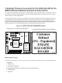
5. Enabling I2S Device Connectivity On The 21065L EZ-LAB Via The
EMAFE (Enhanced Modular Analog Front End) Interface
The 21065L EZ-LAB’s EMAFE connector allows an upgrade path for evaluating present and future I2S-compatible codec’s and
ADC’s (AD18xx, AD7xxx, Crystal Semiconductor converters and digital audio interfaces, multi-media codecs, etc.) with the
ADSP-21065L EZ-LAB Development Board.
The analog front end devices can be placed on a daughter board (thus being modular). Each EMAFE daughter board can have
its own back plate to allow different input connections (i.e. RCA jack, mic in, speaker out, etc.). The daughter board can be
attached to the ADSP-21065L Digital Signal Processor Development Board by a single 96 pin right angle mounted male
connector and two mechanical standoffs to give stability to the entire arrangement when the daughter board and 21065L EZLAB are being attached. The 21065L EZ-LAB has a 96 pin right angle mounted female connector.
Figure 10. ADSP-21065L EZ-LAB EMAFE Interface
ADSP-21065L EZ-LAB EVALUATION BOARD
FLAGIN1 FLAGIN2 FLAGIN3 FLAGIN4
IRQ
Standoff
FLAGOUTx LED
FLAGOUTx LED
FLAGOUTx LED
FLAGOUTx LED
FLAGOUTx LED
FLAGOUTx LED
IRQ
IRQ
BOOT
EPROM
POWER LED
REG
EMAFE INTERFACE CONNECTOR
POWER
CUSTOM ENHANCED MAFE DAUGHTER BOARD
32 Bit Wide
SDRAM
RESET
REG
a
RS-232
ADSP-21065L
DIGITAL
SIGNAL
PROCESSOR
JTAG
OSC
EMAFE
INTERFACE
CONTROL
LOGIC
AND
AD1819A
SOUNDPORT
LOGIC
EXPANSION CONNECTOR
LINE IN
EXPANSION CONNECTOR
LINE OUT
MIC IN
Customer
Defined
(I2S - Populated)
EMAFE
DAUGHTER
BOARD
Standoff
EMAFE Signal Description:
The EZ-LAB's EMAFE 96 pin connector routes the following signals from the ADSP-21065L to the EMAFE daughter board.
16 Data lines.
8
Address lines.
3
Parallel Bus Control lines.
16 Synchronous Serial Port lines – Which Gives Access for I2S Connectivity
1
Interrupt output
1
Flag input.
The EMAFE 96 pin connector also has the following power connections routed from the 21065L EZ-LAB Development Board
to the EMAFE interface.
VDD1
Digital power ( +5V, 150 mA).
VDD2
Digital power ( +3.3V, 150 mA).
+3VA
Analog power (100 mA, clean).
+5VA
Analog power (100 mA, clean).
There is one 3x32 pin right angle connector on the EZ-LAB with female pins. The is mounted on the right end of EZ-LAB
board. The EMAFE daughter board should have one 3x32 pin connector with male pins on the left side of the board.
EMAFE Functional Description
The parallel communication between the ADSP-21065L on the EZ-LAB Board and the EMAFE interface consists of some
control logic for the control lines (MC, RD, WR, CS, etc.), an 8-bit latch that will store the address information (MA[7:0]) and
a transceiver buffer for the data lines (MD[15:0]). The address lines are latched and the data lines are buffered to reduce digital
noise on the MAFE board.
The 2 synchronous serial ports (SPORT0 and SPORT1) from the ADSP-21065L processor is also directly wired to the EMAFE
connector interface pins. Level shifting of serial port signals from the ADSP-21065L processor may be required for 5V (non
3.3V compliant) peripherals on the EMAFE board, or from 5V peripherals on the EMAFE board to the 3.3v (non 5V tolerant)
ADSP-21065L processor. Thus, the EMAFE serial port pins are used to connect to I2S devices on the EMAFE daughter card.
Additional address and data lines can be used for control and status information to various digital audio devices such as
AES/EBU and SP/DIF transmitters and receivers.
6. Using The 21065L EZ-LAB EMAFE Interface For The I2S
Loopback Test
The I2S reference code listed in Appendix A was tested on the Analog Devices 21065L EZ-LAB evaluation board (test case
shown in Figure 11). The example code implements a 'digital wire' test, which consists of looping back incoming ADC data
from the AD1819a SoundPort codec via the SPORT0 I2S interface, and the resulting loopback of audio is sent out of the
AD1819a DACs. The implementation sets up transmit and receive DMA chaining on SPORT1 to transfer data between the
DSP and the AD1819a, while also setting up transmit and receive DMA chaining on SPORT0 for the I2S master transmitter and
the slave receiver. To enable the connection, wire-wrap was used to connect the SPORT0 transmit data, word select and serial
clock pins from the transmitter to the receiver. When connecting the SPORT0 pin, be careful to use a short, straight wire to
ensure the best possible noise immunity.
Figure 11.
21065L EZ-LAB EMAFE I2S Audio Loopback Example
I2S transmitter
wired back to I2S
receive
a
a
AD1819A
ADSP21065L
SPORT1
TFS0
TCLK
DT0A
RFS0
RCLK
DR0A
I2S Master
SPORT0
I2S Slave
Stereo Line
Out
Left/Right
Speakers
Stereo Mic
EMAFE
Connector
Figure 12.
21065L EZ-LAB I2S ‘Digital Wire’ DMA & Memory Signal Paths
SPORT1 ADC RX DMA Buffer
RX_BUF [5]
Tag Slot
SPORT0 I2S TX Master
DMA Buffer
Reg Addr
RX1
Reg Data
SPORT1 ADC
data,
RX1 register
ADC Left
ADC Right
I2S_TX_BUF [2]
DM Audio Data Holders
DM(Left_Channel_In)
I2S TX Left
DM(Right_Channel_In)
I2S TX Right
TX0
SPORT1 DAC TX DMA Buffer
TX_BUF [5]
DT0A
SPORT1 EMAFE
Loopback
DR0A
Tag Slot
RX0
Codec Addr
DM Audio Data Holders
TX1
Codec Data
SPORT1 DAC
data,
TX1 register
DAC Left
DAC Right
I2S RX Left
DM(Left_Channel_Out)
I2S RX Right
DM(Right_Channel_Out)
I2S_RX_BUF [2]
SPORT0 I2S TX Master DMA Buffer
Table 10. Serial Port I2S Channel Assignments, DMA Buffer Relationships
The DSP SPORT I2S Mode Time Slot Map for the SPORT0 Channel A I2S Loopback Example
Channel
'0'
'1'
Slave I2S Device, Receiver (DR0)
Left Channel Receive
Right Channel Receive
Master I2S Device, Transmitter
Left Channel Transmit
Right Channel Transmit
(DT0)
Table 11. ADSP-2106x SPORT0 Ch. A DMA Buffers Used in the Example SPORT0 I2S Driver (Appendix A):
i2s_rx_buf[2] - SPORT0 DMA receive I2S buffer
WS
0
1
Description
I2S RX Left Channel
I2S RX Right Channel
DSP Data Memory Direct Address
DM(i2s_rx_buf + 0) = DM(i2s_rx_buf + LEFT)
DM(i2s_rx_buf + 1) = DM(i2s_rx_buf + RIGHT)
i2s_tx_buf[2] - SPORT0 DMA transmit I2S buffer
WS
0
1
Description
I2S TX Left Channel
I2S TXRight Channel
DSP Data Memory Direct Address
DM(i2s_tx_buf + 0) = DM(i2s_tx_buf + LEFT)
DM(i2s_tx_buf + 1) = DM(i2s_tx_buf + RIGHT)
6.1 Processing 16-bit or 24-bit data in 1.31 Fractional Format or IEEE Floating Point
Format
Data that is received or transmitted in the SPORT0 ISR is in a binary, 2's complement format. The DSP interprets the data in
fractional format, where all #s are between -1 and 0.9999999. Initially, the serial port places the data into internal memory in
data bits D0 to D15 for 16 bit data and D0 to D23 for 24-bit data. In order to process the fractional data in 1.31 format, the
processing routine first shifts the data up by 16 bits (or 8-bits for 24-bit data) so that it is left-justified in the upper data bits D16
to D31 (or D8 to D31 for 24 bit data). This is necessary to take advantage of the fixed-point multiply/accumulator's fractional
1.31 mode, as well as offer an easy reference for converting from 1.31 fractional to floating point formats. This also guarantees
that any quantization errors resulting from the computations will remain well below the 16 bit or 24-bit result and thus below
the DAC Noise Floor. After processing the data, the DSP shifts the 1.31 result down so that the data is truncated to a 1.15 or
1.23 number. This fractional result is then sent to the DAC. Below are example instructions to demonstrate shifting of data
before and after the processing of data on the left channel when processing 16-bit samples:
32-bit Fixed Point Processing
r1 = dm(rx0a_buf + 0);
r1= lshift r1 by 16;
dm(Left_Channel)=r1;
/*
/* get ADC left channel input sample */
/* shift up to MSBs to preserve sign */
/* save to data holder for processing */
Process data here, data is processed in 1.31 format */
r15 = dm(Left_Channel);
r15 = lshift r6 by -16;
dm(tx0a_buf + 0) = r15;
/* get channel 1 output result */
/* put back in bits 0..15 for SPORT tx */
/* output left result to DAC */
To convert to a floating point number, or from a floating point number back to a fixed point number, the ADSP-21065L
supports single-cycle data format conversion between fixed and floating point numbers as shown below:
32-bit Floating Point Processing
To convert between our assumed 1.31 fractional number and IEEE floating point math, here are some example
assembly instructions. This assumes that our ADC data has already been converted to floating point
format, as shown above:
r1 = -31;
<-- scale the sample to the range of +/-1.0
r0 = DM(Left_Channel);
f0 = float r0 by r1;
[Call Floating_Point_Algorithm]
r1 = 31;
<-- scale the result back up to MSBs
r8 = fix f8 by r1;
DM(Left_Channel) = r8;
REFERENCES
The following sources contributed information to this applications note:
1. ADSP-21065L SHARC User’s Manual, Analog Devices, Inc,.
First Edition (82-001833-01, Analog-Devices, September 1998)
2. Philips I2S Bus Specification, Philips Semiconductor,.
Electronic components and materials catalog (no data)
A.1 21065L EZ-LAB Example - SPORT0 I2S Mode, DMA Initializations
/* ********************************************************************************************** */
/*
SPORT0 I2S Mode Initialization
*/
/*
*/
/*
These assembly routines set up the ADSP-21065L SPORT0 registers for I2S mode for
*/
/*
transmitting and recieving of data at 48 KHz. This routine will set up DMA chaining on
*/
/*
SPORT0 to recieve data coming from the AD1819a, do an I2S loopback on SPORT0 on the
*/
/*
incoming AD1819a audio data, and the results of the loopback will be sent to the AD1819a */
/*
DACs. The I2S routines can be used as a programming reference to test the 'digital wire' */
/*
of the I2S ports.
*/
/*
*/
/*
By: John Tomarakos
*/
/*
ADI DSP Applications
*/
/*
Rev 1.0, 12/15/98
*/
/*
Rev 1.1, 1/11/98
*/
/*
*/
/* ********************************************************************************************* */
/* ADSP-21065L System Register bit definitions */
#include
"def21065l.h"
#include
"new65Ldefs.h"
.GLOBAL
.GLOBAL
.GLOBAL
.GLOBAL
Program_DMA_Controller_SPT0;
Program_I2Smode_SPORT0_Registers;
i2s_rx_buf;
i2s_tx_buf;
.segment /dm
dm_I2S;
/* define buffer size to match I2S TDM stereo channels */
#define
STEREO_LR
2
.var i2s_rx_buf[STEREO_LR];
.var i2s_tx_buf[STEREO_LR];
/* stereo I2S receive buffer */
/* stereo I2S transmit buffer */
.var i2s_rcv_tcb[8] = 0, 0, 0, 0, 0, 2, 1, 0;
.var i2s_xmit_tcb[8] = 0, 0, 0, 0, 0, 2, 1, 0;
/* receive tcb */
/* transmit tcb */
.endseg;
.segment /pm
/*
/*
/*
/*
pm_code;
---------------------------------------------------------------------------------------------*/
Sport0 Control Register Programming
*/
I'squared'S Mode dma w/ chain, erly fs, act hi fs, fall edge, no pack, data=16/big/zero
*/
---------------------------------------------------------------------------------------------*/
Program_I2Smode_SPORT0_Registers:
/* sport0 receive control register */
R0 = 0x000D09F1;
/* slave mode, slen = 32 , sden_A & schen_A enabled */
dm(SRCTL0) = R0;
/* sport 0 receive control register */
/* sport0 transmit control register */
R0 = 0x000D0DF1;
/* master mode, data depend, slen = 32, sden_A & schen_A enabled */
dm(STCTL0) = R0;
/* sport 0 transmit control register */
/* sport0 I2S word select (transmit frame sync) divide register
We want to set up a frame sync of 96KHz, since this is twice of 48 KHz
Data coming from the AD1819a is 48 KHz, so to send both left and right data via the
I2S ports, we need to send the stereo data at a rate = 2x of the AD1819a Fs. The TFS will
toggle every 96 K, but both left and right I2S data is being transmitted at a rate of 48K
equivalent to the AD1819a frame rate
The SPORT0 ISR will be called at a rate of 48K since the I2S DMA buffers are 2 words deep
*/
R0 = 0x007C0004;
/* TCLKDIV=[2xfCLKIN(60MHz)/SCLKfreq(12MHz)]-1 = 0x0004v */
dm(TDIV0) = R0;
/* TFSDIV=[TCLKfrq(12 MHz)/TFSfrq(96.0K)]-1 = 124 = 0x007C */
/* sport0 I2S receive word select divide register */
R0 = 0x00000000;
dm(RDIV0) = R0;
/* sport0 receive and transmit multichannel word enable registers */
R0 = 0x00000000;
/* multichannel mode disabled */
dm(MRCS0) = R0;
dm(MTCS0) = R0;
/* sport0 transmit and receive multichannel companding enable registers */
R0 = 0x00000000;
/* no companding */
dm(MRCCS0) = R0;
/* no companding on receive */
dm(MTCCS0) = R0;
/* no companding on transmit */
RTS;
/*-------------------------------------------------------------------------------- */
/*
DMA Controller Programming For SPORT0 I2S Tx and Rx
*/
/*
*/
/*
Setup SPORT0 I2S for DMA Chaining:
*/
/*-------------------------------------------------------------------------------- */
Program_DMA_Controller_SPT0:
r1 = 0x0001FFFF;
/* cpx register mask */
/* sport0 dma control tx chain pointer register */
r0 = i2s_tx_buf;
dm(i2s_xmit_tcb + 7) = r0;
/* internal dma address used for chaining*/
r0 = 1;
dm(i2s_xmit_tcb + 6) = r0;
/* DMA internal memory DMA modifier */
r0 = 2;
dm(i2s_xmit_tcb + 5) = r0;
/* DMA internal memory buffer count */
r0 = i2s_xmit_tcb + 7;
/* get DMA chaining internal mem pointer containing tx_buf address */
r0 = r1 AND r0;
/* mask the pointer */
r0 = BSET r0 BY 17;
/* set the pci bit */
dm(i2s_xmit_tcb + 4) = r0;
/* write DMA transmit block chain pointer to TCB buffer */
dm(CPT0A) = r0;
/* transmit block chain pointer, initiate tx0 DMA transfers */
/* sport0 dma control
r0 = i2s_rx_buf;
dm(i2s_rcv_tcb + 7) =
r0 = 1;
dm(i2s_rcv_tcb + 6) =
r0 = 2;
dm(i2s_rcv_tcb + 5) =
r0 = i2s_rcv_tcb + 7;
r0 = r1 AND r0;
r0 = BSET r0 BY 17;
dm(i2s_rcv_tcb + 4) =
dm(CPR0A) = r0;
RTS;
.endseg;
rx chain pointer register */
r0;
/* internal dma address used for chaining */
r0;
/* DMA internal memory DMA modifier */
r0;
/* DMA internal memory buffer count */
r0;
/*
/*
/*
/*
mask the pointer */
set the pci bit */
write DMA receive block chain pointer to TCB buffer*/
receive block chain pointer, initiate rx0 DMA transfers */
A.2 SPORT0 I2S Receive Interrupt Service Routine
/* **************************************************************************************************
SPORT0 I2S RX INTERRUPT SERVICE ROUTINE
Receives loopback data from SPORT0 I2S TX pins via SPORT0 I2S RX and then sends the audio data back the
output channel locations for the AD1819A Stereo DAC routine.
*****************************************************************************************************
Serial Port 0 Transmit Interrupt Service Routine performs arithmetic computations on SPORT0 receive
data buffer (rx_buf) and sends results to SPORT0 transmit data buffer (tx_buf)
i2s_rx_buf[2] - DSP SPORT0 I2S recieve buffer
channel Description
------ -------------------------------------0
I2S Left Channel Data
1
I2S Right Channel Data
DSP Data Memory Address
------------------------------------------------DM(i2s_rx_buf + 0) = DM(i2s_rx_buf + LEFT)
DM(i2s_rx_buf + 1) = DM(i2s_rx_buf + RIGHT)
i2s_tx_buf[2] - DSP SPORT0 I2S transmit buffer
channel # Description
------ -------------------------------------0
I2S Left Channel TX Data
1
I2S Right Channel TX Data
DSP Data Memory Address
-------------------------------------------------DM(i2s_tx_buf + 0) = DM(i2s_tx_buf + LEFT)
DM(i2s_tx_buf + 1) = DM(i2s_rx_buf + RIGHT)
*****************************************************************************************************/
/* ADSP-21065L System Register bit definitions */
#include
"def21065l.h"
#include
"new65Ldefs.h"
/* AD1819 SPORT0 Rx and Tx Timeslot Definitions */
#define
LEFT
0
#define
RIGHT
1
.GLOBAL
.EXTERN
.EXTERN
.EXTERN
.EXTERN
.EXTERN
.EXTERN
.EXTERN
Process_I2S_Stereo_Data;
Left_Channel_In;
Right_Channel_In;
Left_Channel_Out;
Right_Channel_Out;
i2s_rx_buf;
i2s_tx_buf;
Slapback_Echo;
.segment /dm
.VAR
.VAR
.VAR
dm_data;
I2S_Left_Channel;
I2S_Right_Channel;
I2S_timer = 0x00000000;
.endseg;
.segment /pm pm_code;
Process_I2S_Stereo_Data:
bit set mode1 SRRFL;
nop;
/* enable secondary registers R0-R7 */
/* 1 cycle latency writing to Mode1 register */
get_prior_i2s_tx_data:
/* get previous SPORT0 loopback'ed i2s left and right data */
/* we are getting I2S data that was send in our previous SPORT0 interrupt, and then
feeding this audio data back to the AD1819a DACs */
r0 = dm(i2s_rx_buf + LEFT);
/* Get i2s left channel rx data */
r1 = dm(i2s_rx_buf + RIGHT);
/* Get i2s right channel rx data */
send_audio_to_AD1819a:
dm(Left_Channel_Out) = r0;
dm(Right_Channel_Out) = r1;
/* transmit new AD1819a ADC data out of SPORT0 i2s port */
tx_ADC_data_out_I2s:
r0 = dm(Left_Channel_In);
/* get AD1819a Left ADC channel data */
r1 = dm(Right_Channel_In);
/* get AD1819 Right ADC channel data */
dm(i2s_tx_buf + LEFT) = r0;
/* send i2s left channel tx data */
dm(i2s_tx_buf + RIGHT) = r1;
/* send i2s right channel tx data */
i2s_tx_done:
rti(db);
bit clr mode1 SRRFL;
nop;
/* return from interrupt, delayed branch */
/* restore primary registers R0-R7 */
/* 1 cycle latency writing to MODE1 register */
/* ----------------------------------------------------------------------------------------- */
.endseg;
APPENDIX B: Example Assembly Driver for interfacing to
24-bit, 96 kHz AKM Semiconductor ADCs and DACs.
This example was written and tested on Bittware Research Systems’Spinner ADSP-21065L Audio OEM Board. For
information on that audio OEM development system, contact Bittware at 1-800-848-0436, or search their web site at
www.bittware.com. This development board contains the following features:
•
•
•
•
•
•
•
•
2 or 4 channels of 24-bit, 96 kHz A/D and D/A
96 kHz AES/EBU digital audio interface
Single or dual 180 MFLOPS ADSP-21065L processors
1M FLASH memory with optional boot loading
PCI interface or standalone operation
4M (16MB) SDRAM
Dual 16550-type UART
Digital I/O port
Visual DSP 4.0 Project Files
B.1 SPORT0 I2S Initialization Routine for 2 x Stereo ADCs, 2 x Stereo DACs
/* ********************************************************************************************** */
/*
SPORT0 I2S Mode Initialization
*/
/*
*/
/*
These assembly routines set up the ADSP-21065L SPORT0 registers for I2S mode for
*/
/*
transmitting and recieving of data in slave mode at 96 KHz.
*/
/*
*/
/*
By: John Tomarakos
*/
/*
ADI DSP Applications
*/
/*
Rev 1.0, 1/27/98
*/
/*
*/
/* ********************************************************************************************** */
/* ADSP-21065L System Register bit definitions */
#include
"def21065l.h"
#include
"new65Ldefs.h"
.GLOBAL
.GLOBAL
.GLOBAL
.GLOBAL
.GLOBAL
.GLOBAL
.segment /dm
Program_DMA_Controller_SPT0;
Program_I2Smode_SPORT0_Registers;
rx0a_buf;
tx0a_buf;
rx0b_buf;
tx0b_buf;
dm_I2S;
/* define buffer size to match I2S TDM stereo channels */
#define
STEREO_LR
2
#define
.var
.var
.var
.var
ID2
0x00000200
rx0a_buf[STEREO_LR];
rx0b_buf[STEREO_LR];
tx0a_buf[STEREO_LR];
tx0b_buf[STEREO_LR];
.var rcv0a_tcb[8]
.var rcv0b_tcb[8]
/*
/*
/*
/*
stereo
stereo
stereo
stereo
I2S
I2S
I2S
I2S
/* SYSTAT bit mask for SHARC B with ID = 2 */
primary receive a buffer */
secondary receive b buffer */
primary transmit a buffer */
secondary transmit b buffer */
= 0, 0, 0, 0, 0, 2, 1, 0;
= 0, 0, 0, 0, 0, 2, 1, 0;
/* receive a tcb */
/* receive b tcb */
.var xmit0a_tcb[8] = 0, 0, 0, 0, 0, 2, 1, 0;
.var xmit0b_tcb[8] = 0, 0, 0, 0, 0, 2, 1, 0;
/* transmit a tcb */
/* transmit b tcb */
.endseg;
.segment /pm
pm_code;
/* ---------------------------------------------------------------------------------------------*/
/* Sport0 Control Register Programming
*/
/* I'squared'S Mode dma w/ chain, slave mode, no pack, data=24/big/zero
*/
/* ---------------------------------------------------------------------------------------------*/
Program_I2Smode_SPORT0_Registers:
/* check if the DSP has ID = 2, If ID=2, then clear flag1 */
/* This will activate a direct connection between that processor, and the AKM ADCs and DACs */
R0 = dm(SYSTAT);
R1 = ID2;
R0 = R0 AND R1;
IF EQ jump set_spt_regs;/* if ID=1, keep flag0 set, enables SPORT to SHARC A */
bit clr astat FLG1;
/* clr flag 0 LED, enables SPORT to SHARC B */
set_spt_regs:
/* sport0 receive control register */
R0 = 0x013C0971;
/* slave mode, slen = 24, sden_A & schen_A & sden_B & schen_B enabled */
dm(SRCTL0) = R0;
/* sport 0 receive control register */
/* sport0 transmit control register */
R0 = 0x017C8971;
/* slave mode, slen = 24, sden_A & schen_A & sden_B & schen_B enabled */
dm(STCTL0) = R0;
/* sport 0 transmit control register */
/* sport0 I2S word select (transmit frame sync) divide register */
R0 = 0x00000000;
/* TCLKDIV=[2xfCLKIN(60MHz)/SCLKfreq(12MHz)]-1 */
dm(TDIV0) = R0;
/* TFSDIV=[TCLKfrq(12 MHz)/TFSfrq(96.0K)]-1 */
/* sport0 I2S receive word select divide register */
R0 = 0x00000000;
dm(RDIV0) = R0;
/* sport0 receive and transmit multichannel word enable registers */
R0 = 0x00000000;
/* multichannel mode disabled */
dm(MRCS0) = R0;
dm(MTCS0) = R0;
/* sport0 transmit and receive multichannel companding enable registers */
R0 = 0x00000000;
/* no companding */
dm(MRCCS0) = R0;
/* no companding on receive */
dm(MTCCS0) = R0;
/* no companding on transmit */
RTS;
/*----------------------------------------------------------------------------------*/
/*
DMA Controller Programming For SPORT0 I2S Tx and Rx
*/
/*
*/
/*
Setup SPORT0 I2S for DMA Chaining:
*/
/*----------------------------------------------------------------------------------*/
Program_DMA_Controller_SPT0:
r1 = 0x0001FFFF;
/* cpx register mask */
/* sport0 dma channel a control tx chain pointer register */
r0 = tx0a_buf;
dm(xmit0a_tcb + 7) = r0;
/* internal dma address used for chaining*/
r0 = 1;
dm(xmit0a_tcb + 6) = r0;
/* DMA internal memory DMA modifier */
r0 = 2;
dm(xmit0a_tcb + 5) = r0;
/* DMA internal memory buffer count */
r0 = xmit0a_tcb + 7;
/* get DMA chaining int mem pointer containing tx_buf addr */
r0 = r1 AND r0;
/* mask the pointer */
r0 = BSET r0 BY 17;
/* set the pci bit */
dm(xmit0a_tcb + 4) = r0;
/* write DMA transmit block chain pointer to TCB buffer */
dm(CPT0A) = r0;
/* transmit block chain pointer, initiate tx0 DMA xfers */
/* sport0 dma channel b control tx chain pointer register */
r0 = tx0b_buf;
dm(xmit0b_tcb + 7) = r0;
/* internal dma address used for chaining*/
r0 = 1;
dm(xmit0b_tcb + 6) = r0;
/* DMA internal memory DMA modifier */
r0 = 2;
dm(xmit0b_tcb + 5) = r0;
/* DMA internal memory buffer count */
r0 = xmit0b_tcb + 7;
/* get DMA chaining int mem pointer containing tx_buf addr */
r0 = r1 AND r0;
/* mask the pointer */
r0 = BSET r0 BY 17;
/* set the pci bit */
dm(xmit0b_tcb + 4) = r0;
/* write DMA transmit block chain pointer to TCB buffer */
dm(CPT0B) = r0;
/* transmit block chain pointer, initiate tx0 DMA x-fers */
/* sport0 dma channel a control rx chain pointer register */
r0 = rx0a_buf;
dm(rcv0a_tcb + 7) = r0;
/* internal dma address used for chaining */
r0 = 1;
dm(rcv0a_tcb + 6) = r0;
/* DMA internal memory DMA modifier */
r0 = 2;
dm(rcv0a_tcb + 5) = r0;
/* DMA internal memory buffer count */
r0 = rcv0a_tcb + 7;
r0 = r1 AND r0;
/* mask the pointer */
r0 = BSET r0 BY 17;
/* set the pci bit */
dm(rcv0a_tcb + 4) = r0;
/* write DMA receive block chain pointer to TCB buffer*/
dm(CPR0A) = r0;
/* receive block chain pointer, initiate rx0 DMA transfers */
/* sport0 dma channel b control rx chain pointer register */
r0 = rx0b_buf;
dm(rcv0b_tcb + 7) = r0;
/* internal dma address used for chaining */
r0 = 1;
dm(rcv0b_tcb + 6) = r0;
/* DMA internal memory DMA modifier */
r0 = 2;
dm(rcv0b_tcb + 5) = r0;
/* DMA internal memory buffer count */
r0 = rcv0b_tcb + 7;
r0 = r1 AND r0;
/* mask the pointer */
r0 = BSET r0 BY 17;
/* set the pci bit */
dm(rcv0b_tcb + 4) = r0;
/* write DMA receive block chain pointer to TCB buffer*/
dm(CPR0B) = r0;
/* receive block chain pointer, initiate rx0 DMA transfers */
RTS;
.endseg;
B.2 SPORT0 Interrupt Processing Routine – AD/DA Audio Loopback
Figure 13. Dual ADC/DAC Software Driver ISR Data Flow Structure
SPORT0 ADC 1 RX0A DMA Buffer
RX0A_BUF [2]
I2S Left
I2S Right
RX0A
SPORT0 ADC
data
RX0A register
DM Audio Data
DM( Left_ChannelA_In)
DM( Right_ChannelA_In)
DSP Audio
Algorithm
SPORT0 DAC 1 TX0A DMA Buffer
TX0A
TX0A_BUF [2]
DM Audio Data
I2S Left
I2S Right
DM( Left_ChannelA_Out)
SPORT0 DAC
data
TX0A register
DM( Right_ChannelA_Out)
SPORT0 ADC 2 RX0B DMA Buffer
RX0B_BUF [2]
I2S Left
I2S Right
RX0B
SPORT0 ADC
data
RX0B
DM Audio Data
DM(Left_ChannelB_In)
DM(Right_ChannelB_In)
Loopback
Left & Right
Audio
Samples
SPORT0 DAC 2 TX0B DMA Buffer
TX0B_BUF [2]
TX0B
SPORT0 DAC
data
TX0B
I2S Left
I2S Right
DM Audio Data
DM( Left_ChannelB_Out)
DM( Right_ChannelB_Out)
/* **************************************************************************************************
SPORT0 I2S RX INTERRUPT SERVICE ROUTINE
Receives AKM ADC data from SPORT0 I2S RX pins and then sends the audio data back out to the AKM DAC
Line Outputs
*****************************************************************************************************
Serial Port 1 Transmit Interrupt Service Routine performs arithmetic computations on SPORT1 receive
data buffer (rx_buf) and sends results to SPORT1 transmit data buffer (tx_buf)
rx0a_buf[2], tx0b_buf[2] - DSP SPORT0 I2S recieve buffers
channel Description
DSP Data Memory Address
------ -------------------------------------------------------------------------------------0
I2S Left Channel Data
DM(rx_buf + 0) = DM(rx0a_buf + LEFT)
1
I2S Right Channel Data
DM(rx_buf + 1) = DM(rx0a_buf + RIGHT)
tx0a_buf[2], tx0b_buf[2] - DSP SPORT0 I2S transmit
channel # Description
------ -------------------------------------0
I2S Left Channel TX Data
1
I2S Right Channel TX Data
buffers
DSP Data Memory Address
-------------------------------------------------DM(tx0a_buf + 0) = DM(rx0a_buf + LEFT)
DM(tx0a_buf + 1) = DM(tx0a_buf + RIGHT)
*****************************************************************************************************/
/* ADSP-21065L System Register bit definitions */
#include
"def21065l.h"
#include
"new65Ldefs.h"
/* AD1819 SPORT0 Rx and Tx Timeslot Definitions */
#define
LEFT
0
#define
RIGHT
1
.GLOBAL
.GLOBAL
.GLOBAL
.GLOBAL
.GLOBAL
.GLOBAL
.GLOBAL
.GLOBAL
.GLOBAL
.EXTERN
.EXTERN
.EXTERN
.EXTERN
.EXTERN
.segment /dm
Process_AKM_I2S_Stereo_Data;
Left_ChannelA_In;
Right_ChannelA_In;
Left_ChannelA_Out;
Right_ChannelA_Out;
Left_ChannelB_In;
Right_ChannelB_In;
Left_ChannelB_Out;
Right_ChannelB_Out;
rx0a_buf;
tx0a_buf;
rx0b_buf;
tx0b_buf;
Auto_Double_Tracking;
dm_data;
/* stereo-channel data holders - used for DSP processing of audio data */
.VAR
Left_ChannelA_In;
.VAR
Right_ChannelA_In;
.VAR
Left_ChannelB_In;
.VAR
Right_ChannelB_In;
.VAR
.VAR
.VAR
.VAR
Left_ChannelA_Out;
Right_ChannelA_Out;
Left_ChannelB_Out;
Right_ChannelB_Out;
.VAR
I2S_timer = 0x00000000;
.endseg;
.segment /pm pm_code;
Process_AKM_I2S_Stereo_Data:
/* enable secondary registers R0-R7 */
nop;
get_ADC_i2s_rx_data:
/* Get SPORT0 I2S
r0 = dm(rx0a_buf + LEFT);
r0 = lshift r0 by 8;
r1 = dm(rx0a_buf + RIGHT);
r1 = lshift r1 by 8;
/* save for audio processing */
dm(Left_ChannelA_In) = r0;
dm(Right_ChannelA_In) = r1;
/* Get SPORT0 I2S channelB ADC data */
r0 = dm(rx0b_buf + LEFT);
r0 = lshift r0 by 8;
r1 = dm(rx0b_buf + RIGHT);
r1 = lshift r1 by 8;
dm(Left_ChannelB_In) = r0;
dm(Right_ChannelB_In) = r1;
/* loop-back unaltered ADC data */
dm(Left_ChannelB_Out) = r0;
dm(Right_ChannelB_Out) = r1;
/* Get i2s right channel rx data */
/* shift up to MSBs to preserve sign */
/*
/*
/*
/*
Get i2s left channel rx data */
shift up to MSBs to preserve sign */
Get i2s right channel rx data */
shift up to MSBs to preserve sign */
/* -------------------------------------------------------------------------------------------- */
/*
user_applic( ) - User Applications Routines
*/
/*
*** Insert DSP Algorithms Here ***
*/
/*
*/
/*
Input L/R Data Streams - DM(Left_Channel_In) DM(Right_Channel_In)
*/
/*
Output L/R Results
- DM(Left_Channel_Out) DM(Right_Channel_Out)
*/
/*
*/
/*
These left/right data holders are used to pipeline data through
multiple modules, and */
/*
can be removed if the dsp programmer needs to save instruction cycles
*/
/*
~~~~~~~~~~~~~~~~~~~~~~~~~~~~~~~~~~~~~~~~~~~~~~~~~~~~~~~~~~~~~~~~~~~~~~~~~~~~~~~~~~~~~
*/
/*
Coding TIP:
*/
/*
The samples from the AKM ADCs are 24-bit and are in the lower 24 bits of the the 32-bit
*/
/*
word. They are shifted to the most significant bit positions in order to preserve the
*/
/*
sign of the samples when they are converted to floating point numbers. The values are
*/
/*
also scaled to the range +/-1.0 with the integer to float conversion
*/
/*
(f0 = float r0 by r1).
*/
/*
*/
/*
To convert between our assumed 1.31 fractional number and IEEE floating point math,
*/
/*
here are some example assembly instructions ...
*/
/*
*/
/*
r1 = -31
<-- scale the sample to the range of +/-1.0
*/
/*
r0 = DM(Left_Channel);
*/
/*
f0 = float r0 by r1;
*/
/*
[Call Floating_Point_Algorithm]
*/
/*
r1 = 31;
<-- scale the result back up to MSBs
*/
/*
r8 = fix f8 by r1;
*/
/*
DM(Left_Channel) = r8;
*/
/* ---------------------------------------------------------------------------------------------- */
user_applic:
call (pc, Auto_Double_Tracking);
/* ---- DSP processing is finished, now playback results to DACs ---- */
tx_audio_data_out_I2S:
/* transmit channel A audio data out of SPORT0 i2s port tx0A pins */
{r0 = dm(i1,m1);}
/* get sine data from 4K lookup table */
{r1 = dm(i2,m2);}
/* get sine data from 4K lookup table */
r0 = dm(Left_ChannelA_Out);
/* get Left Audio channel data */
r1= dm(Right_ChannelA_Out);
/* get Right Audio channel data */
r0 = lshift r0 by -8;
/* put back in bits 0..23 for SPORT tx */
r1 = lshift r1 by -8;
/* put back in bits 0..23 for SPORT tx */
dm(tx0a_buf + LEFT) = r0;
/* send i2s left channel tx data */
/* send i2s right channel tx data */
transmit channel B audio data out of SPORT0 i2s port tx0A pins */
r0 = dm(
/* get Left ADC channel data */
r0 =
/* put back in bits 0..23 for SPORT tx */
Right_ChannelB_Out);
/* get Right ADC channel data */
lshift r1 by -8;
/* put back in bits 0..23 for SPORT
dm(tx0b_buf + LEFT) = r0;
/* send i2s left channel
dm(tx0b_buf + RIGHT) = r1;
/* send i2s right channel
i2s_tx_done:
r0=dm(I2S_timer);
r0=r0+1;
.
/*
/*
/*
/*
increment count */
save updated count */
return from interrupt, delayed branch */
restore primary registers R0-R7 */
rti(
bit
nop;
/* ----------------------------------------------------------------------------------------- */
;
Disclaimer
Information furnished by Analog Devices, Inc., is believed to be accurate and reliable. However, no responsibility is assumed by Analog
Devices Inc., for its use; nor for any infringements of patents or other rights of third parties which may result from its use. No license is
granted by implication or otherwise under the patent rights of Analog Devices.
Analog Devices Inc. reserves the right to make changes without further notice to any products listed in this document. Analog Devices
makes no warranty, representation or guarantee regarding the suitability of its DSP products for any particular application, nor does Analog
Devices assume any liability arising out of the application or use of our DSP-based products, and specifically disclaims any and all liability,
including without limitation consequential or incidental damages.
Operating parameters such as temperature and voltage can and do vary in different applications. All operating parameters as specified in
Analog Devices data sheets must be validated for each customer application by customer’s technical experts. Analog Device's DSP-based
products are not designed, intended, or authorized for use as components in which the failure of the Analog Devices product could create a
situation where personal injury or death may occur. If the Buyer/Designer uses ADI products for any unintended or unauthorized application,
then Analog Devices cannot be held responsible