1
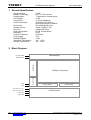
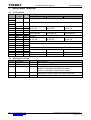
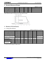
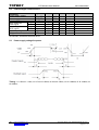
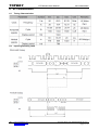
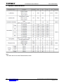
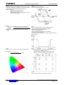
LMT150DNGFWD LCD Module User Manual Prepared by: Checked by: Approved by: Date: Date: Yang Date: 2012-09-10 Rev. 0.1 URL: Descriptions Preliminary www.topwaydisplay.com www.topwaysz.com Release Date 2012-09-10 Document Name: LMT150DNGFWD-Manual-Rev0.1 Page: 1 of 10 TOPWAY LCD Module User Manual LMT150DNGFWD Table of Content 1. General Specification ............................................................................................................ 3 2. Block Diagram........................................................................................................................ 3 3. Input/Output Terminals.......................................................................................................... 4 3.1 TFT Terminals........................................................................................................................................................ 4 3.2 BackLight Terminals............................................................................................................................................... 4 4. Absolute Maximum Ratings .................................................................................................. 5 5. Electrical Characteristics ...................................................................................................... 5 5.1 Driving TFT LCD Panel .......................................................................................................................................... 5 5.2 CCFL Backlight Characteristics.............................................................................................................................. 6 5.3 Power supply voltage Sequence ............................................................................................................................ 6 6. AC Characteristics................................................................................................................. 7 6.1 Timing Characteristics............................................................................................................................................ 7 6.2 Input signal timing chart ......................................................................................................................................... 7 7. Optical Characteristics .......................................................................................................... 8 8. Precautions of using LCD Modules .................................................................................... 10 URL: www.topwaydisplay.com www.topwaysz.com Document Name: LMT150DNGFWD-Manual-Rev0.1 Page: 2 of 10 TOPWAY LCD Module User Manual LMT150DNGFWD 1. General Specification Signal Interface : Display Technology : Display Mode : Color Depth: Screen Size : Outline Dimension : LVDS a-Si TFT active matrix Transmissive / Normal White 16.7M 15.0 inch (Diagonal) 326.5x253.5x11.8 (mm) (see Outline DWG for details) 304.128x228.096 (mm) 1024x 3 (RGB) x 768 0.099x0.297 (mm) R.G.B. Vertical Stripe LEDs Anti-Glare 3.3V 12.0V -20 ~ +70°C -30 ~ +80°C Active Area : Number of dots : Dot Pitch : Pixel Configuration : Backlight : Surface Treatment : Logic Supply: Backlight Supply: Operating Temperature : Storage Temperature : 2. Block Diagram LED Backlight BL_VDD, GND GND VDD Power Circuit Gate Driver BLEN, BLADJ 1024(x3) x 768 pixels Source Driver Source Driver D0+, D0-, D1+, D1D2+, D2- , D3+, D3- LVDS interface CLK+, CLKMSL, FRC URL: www.topwaydisplay.com www.topwaysz.com Document Name: LMT150DNGFWD-Manual-Rev0.1 Page: 3 of 10 TOPWAY LCD Module User Manual LMT150DNGFWD 3. Input/Output Terminals 3.1 TFT Terminals Pin No. Pin Name 1 VDD 2 GND 3 4 D05 6 D0+ 7 GND 8 D1D1+ 9 10 GND 11 D212 D+ 13 GND CLK14 15 CLK+ 16 GND 17 D318 D3+ 19 MSL 20 FRC 3.2 Descriptions IO 24Bit LVDS(MAP A) 24Bit LVDS (MAP B) 18Bit LVDS Power Power Supply Power Ground Input Input Power Input Input Power Input Input Power Input Input Power Input Input Input Input Pixel data R2~R7,G2 Ground Pixel data G3~G7,B2~B3 Ground Pixel data B4~B7,DE Ground Pixel clock Pixel data R0~R5,G0 Pixel data G1~G5,B0~B1 Pixel data G1~G5,B0~B1 Pixel data B2~B5,DE Pixel data B2~B5,DE Ground R0~R1,G0~G1,B0~B1 R6~R7,G6~G7,B6~B7 Ground MSL=1 FRC=0 MSL=0,or open FRC=0 MSL=1 FRC=1,or open BackLight Terminals Pin No. 1 2 3 Pin Name BL_VDD GND BLEN IO Power Power Input 4 BLADJ Input 5 NC - URL: Pixel data R0~R5,G0 www.topwaydisplay.com www.topwaysz.com Descriptions Positive Power Supply(12.0V) Power Supply GND (0V) Backlight Driver Control(*1) BLEN=Hi, Backlight Driving Booster enable BLEN=Lo, Backlight Driving Booster disable Backlight dimming control PWM may be used to adjust the output brightness No Connection Document Name: LMT150DNGFWD-Manual-Rev0.1 Page: 4 of 10 TOPWAY LCD Module User Manual LMT150DNGFWD 4. Absolute Maximum Ratings Items Symbol Min. Max. -0.3 Power Voltage VDD +4.0 VIN -0.3 +4.0 Input voltage TOP -20 +70 Operating Temperature Storage Temperature TST -30 +80 Note1: VIN represent D0±, D1±, D2±, D3±, CLK± Note2: Recommanded Temperature/Humidity Graph as follow Unit V V C C GND=0V, TOP=25C Condition GND = 0V GND= 0V No Condensation No Condensation Relative Humidity(%RH) Temperature ℃ 5. Electrical Characteristics 5.1 Driving TFT LCD Panel Items Symbol MIN. Power supply voltage VDD 3.0 Power supply current IDD Permissible ripple voltage VRP Differential input voltage |Vid| 250 VTL -100 Differential input threshold voltage for LVDS receiver VTH Input voltage width for Vi 0 LVDS receiver Terminating resistor RT Rush current Irush Input voltage for High VFH 2.0 MSL signals Low VFL 0 *1: All black pattern *2: Common mode voltage for LVDS receiver URL: www.topwaydisplay.com www.topwaysz.com TYP. 3.3 500 - GND=0V, VDD=3.3V, TOP=25C MAX. Unit Note 3.6 V *1 550 mA 100 mV mV 400 mV VCM=1.25V,*2 mV 100 - 1.9 V 100 - 1.5 VCC 0.4 Ω A V V Document Name: LMT150DNGFWD-Manual-Rev0.1 Page: 5 of 10 TOPWAY 5.2 LCD Module User Manual LMT150DNGFWD LED Backlight Characteristics Symbol MIN. TYP. MAX. Unit Note Parameter Power supply voltage V 10.8 12.0 12.6 BL_VDD Power supply current BL_IDD 750 mA Light bar life time Hr 50000 Hr High 2.0 5.0 V Input voltage for PWM signal Low 0 0.4 V Input voltage for High 2.0 5.0 V BRTC signal Low 0 0.4 V PWM frequency Fpwm 200 20K Hz PWM pulse width Tpwm 10 us *1: The operating lifetime is mean time to half-luminance. In case the product works under low temperature environment, the lifetime becomes short. 5.3 Power supply voltage Sequence Timing: t1: 0.5ms<t1 <10ms; t2: 0.5 ms<t2 <50ms; t3: 0ms<t3 <50ms; t4: t4 >1000ms; t5: t5 >200ms; t6: t6 >200ms; URL: www.topwaydisplay.com www.topwaysz.com Document Name: LMT150DNGFWD-Manual-Rev0.1 Page: 6 of 10 TOPWAY LCD Module User Manual LMT150DNGFWD 6. AC Characteristics 6.1 Timing Characteristics 6.2 Input signal timing chart URL: www.topwaydisplay.com www.topwaysz.com Document Name: LMT150DNGFWD-Manual-Rev0.1 Page: 7 of 10 TOPWAY LCD Module User Manual LMT150DNGFWD 7. Optical Characteristics Note: The value above are initial Characteristics Value. URL: www.topwaydisplay.com www.topwaysz.com Document Name: LMT150DNGFWD-Manual-Rev0.1 Page: 8 of 10 TOPWAY LCD Module User Manual Note 1: The data are measured after LEDs are turned on for 5 minutes. LCM displays full white. The brightness is the average value of 9 measured spots. Measurement equipment SR-3A (1°) Measuring condition: - Measuring surroundings: Dark room - Measuring temperature: Ta=25℃. - Adjust operating voltage to get optimum contrast at the center of the display. Note 3: The definition of contrast ratio (Test LCM using SR-3A (1°)): Luminance When LCD is at “White”state Contrast = Ratio(CR) Luminance When LCD is at “Black”state (Contrast Ratio is measured in optimum common electrode voltage) Note 5: Definition of Color of CIE1931 Coordinate and NTSC Ratio. Color gamut: Area of RGB triangle S= Area of NTSC triangle X100% LMT150DNGFWD Note 2: The definition of viewing angle: Refer to the graph below marked by θ and Ф Note 4: Definition of Response time. (Test LCD using BM-7A(2°)): The output signals of photo detector are measured when the input signals are changed from “black”to “white”(falling time) and from “white”to “black”(rising time), respectively. The response time is defined as the time interval between the 10% and 90% of amplitudes.Refer to figure as below. Note 6: The luminance uniformity is calculated by using following formula. △Bp = Bp (Min.) / Bp (Max.)×100 (%) Bp (Max.) = Maximum brightness in 9 measured spots Bp (Min.) = Minimum brightness in 9 measured spots . Note 7: Measured the luminance of white state at center point URL: www.topwaydisplay.com www.topwaysz.com Document Name: LMT150DNGFWD-Manual-Rev0.1 Page: 9 of 10 TOPWAY LCD Module User Manual LMT150DNGFWD 8. Precautions of using LCD Modules Mounting - Mounting must use holes arranged in four corners or four sides. - The mounting structure so provide even force on to LCD module. Uneven force (ex. Twisted stress) should not applied to the module. And the case on which a module is mounted should have sufficient strength so that external force is not transmitted directly to the module. - It is suggested to attach a transparent protective plate to the surface in order to protect the polarizer. It should have sufficient strength in order to the resist external force. - The housing should adopt radiation structure to satisfy the temperature specification. - Acetic acid type and chlorine type materials for the cover case are not desirable because the former generates corrosive gas of attacking the polarizer at high temperature and the latter causes circuit break by electro-chemical reaction. - Do not touch, push or rub the exposed polarizers with glass, tweezers or anything harder than HB pencil lead. Never rub with dust clothes with chemical treatment. Do not touch the surface of polarizer for bare hand or greasy cloth.(Some cosmetics deteriorate the polarizer.) - When the surface becomes dusty, please wipe gently with absorbent cotton or other soft materials like chamois soaks with petroleum benzine. Normal-hexane is recommended for cleaning the adhesives used to attach front / rear polarizers. Do not use acetone, toluene and alcohol because they cause chemical damage to the polarizer. - Wipe off saliva or water drops as soon as possible. Their long time contact with polarizer Operating - The spike noise causes the mis-operation of circuits. It should be within the ± 200mV level (Over and under shoot voltage) - Response time depends on the temperature.(In lower temperature, it becomes longer.) - Brightness depends on the temperature. (In lower temperature, it becomes lower.) And in lower temperature, response time(required time that brightness is stable after turned on) becomes longer. - Be careful for condensation at sudden temperature change. Condensation makes damage to polarizer or electrical contacted parts. And after fading condensation, smear or spot will occur. - When fixed patterns are displayed for a long time, remnant image is likely to occur. - Module has high frequency circuits. Sufficient suppression to the electromagnetic interference shall be done by system manufacturers. Grounding and shielding methods may be important to minimized the interference Electrostatic Discharge Control Since a module is composed of electronic circuits, it is not strong to electrostatic discharge. Make certain that treatment persons are connected to ground through wrist band etc. And don’ t touch interface pin directly. Strong Light Exposure Strong light exposure causes degradation of polarizer and color filter. Storage When storing modules as spares for a long time, the following precautions are necessary. - Store them in a dark place. Do not expose the module to sunlight or fluorescent light. Keep the temperature between 5°C and 35°C at normal humidity. - The polarizer surface should not come in contact with any other object. It is recommended that they be stored in the container in which they were shipped. Protection Film - When the protection film is peeled off, static electricity is generated between the film and polarizer. This should be peeled off slowly and carefully by people who are electrically grounded and with well ionblown equipment or in such a condition, etc. - The protection film is attached to the polarizer with a small amount of glue. If some stress is applied to rub the protection film against the polarizer during the time you peel off the film, the glue is apt tore main on the polarizer. Please carefully peel off the protection film without rubbing it against the polarizer. - When the module with protection film attached is stored for a long time, sometimes there remains a very small amount of glue still on the polarizer after the protection film is peeled off. - You can remove the glue easily. When the glue remains on the polarizer surface or its vestige is recognized, please wipe them off with absorbent cotton waste or other soft material like chamois soaked with normal-hexane. Transportation The LCD modules should be no falling and violent shocking during transportation, and also should avoid excessive press, water, damp and sunshine. URL: www.topwaydisplay.com www.topwaysz.com Document Name: LMT150DNGFWD-Manual-Rev0.1 Page: 10 of 10