1
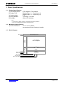
LM1095R-2
LCD Module User Manual
Shenzhen TOPWAY Technology Co., Ltd.
Rev.
0.1
URL:
Descriptions
New release
www.topwaydisplay.com
www.topwaysz.com
Release Date
2006-08-17
Document Name: LM1095R-2-Manual-Rev0.1.doc
Page: 1 of 12
TOPWAY
LCD Module User Manual
LM1095R-2
Table of Content
1.
1.1
1.2
1.3
1.4
Basic Specifications................................................................................................................ 3
Display Specifications............................................................................................................................ 3
Mechanical Specifications ..................................................................................................................... 3
Block Diagram ....................................................................................................................................... 3
Terminal Functions ................................................................................................................................ 4
2.
Absolute Maximum Ratings.................................................................................................... 5
3.
Electrical Characteristics........................................................................................................ 5
3.1
3.2
3.3
4.
4.1
4.2
4.3
4.4
4.5
4.6
5.
URL:
DC Characteristics................................................................................................................................. 5
LED Backlight Circuit Characteristics .................................................................................................... 5
AC Characteristics ................................................................................................................................. 6
Function Specifications .......................................................................................................... 7
Adjusting the Display Contrast .............................................................................................................. 7
Resetting the LCD module..................................................................................................................... 7
Display Pixel Map .................................................................................................................................. 7
Control Data and Command .................................................................................................................. 8
Register Table Summary ....................................................................................................................... 8
Initialization Setting Example............................................................................................................... 11
Design and Handling Precaution ......................................................................................... 12
www.topwaydisplay.com
www.topwaysz.com
Document Name: LM1095R-2-Manual-Rev0.1.doc
Page: 2 of 12
TOPWAY
LCD Module User Manual
LM1095R-2
1. Basic Specifications
1.1
Display Specifications
1) LCD Display Mode
: STN, Negative, Transmissive
2) Display Color
: Display Data = “1” : Dark Gray (*1)
: Display Data = “0” : Light Gray (*2)
3) Viewing Angle
:6H
4) Driving Method
: 1/128 duty, 1/12 bias
5) Backlight
: White LED backlight
Note:
*1. Color tone may slightly change by Temperature and Driving Condition.
*2. The Color is defined as the inactive / background color
1.2
Mechanical Specifications
1) Outline Dimension
: 92.7 x 72.0 x 8.7MAX
see attached Outline Drawing for details
1.3
Block Diagram
LED Backlight Circuit
BLA
COMMON
Driver
Power and
Booster Circuit
VDD, VSS
VOUT, V0
LCD Panel
192 x 128 pixels
SEGMENT
Driver
RA8803
or equivalent
DB0 - DB7
RS, /RD, /WR
BUSY, /CS, /RST
URL:
www.topwaydisplay.com
www.topwaysz.com
Document Name: LM1095R-2-Manual-Rev0.1.doc
Page: 3 of 12
TOPWAY
LCD Module User Manual
1.4 Terminal Functions
Pin
Pin
I/O
No.
Name
1
VOUT
Power
2
V0
Input
3
VDD
Power
4
VSS
Power
5
BUSY
Output
6
7
NC
/CS
Input
8
RS
Input
LM1095R-2
Descriptions
Power Booster Output for V0
LCD Contrast Reference Input
Positive Power Supply
0V Power Supply, GND
Controller busy signal,
MCU should poll this signal before accessing the LCD module
No connection (leave open)
Chip Select Signal
/CS=LOW: Data IO is enabled
Register Select
RS=HIGH: data on DB0 to DB7 is display data
RS=LOW: data on DB0 to DB7 is control data
9
10
11
:
18
19
/WR
/RD
DB0
:
DB7
/RST
Input
Input
I/O
Write enable input, active LOW
Read enable input, active LOW
8-bit bi-directional data bus
Input
Reset Signal:
/RST = L, Reset the LCD Module
/RST = H, Normal Running
20
BLA
Power Positive Power Supply for LED backlight
Note: For enable BUSY output, the REG[A0] D0, D1, D2 or D3 should be set to hi.
URL:
www.topwaydisplay.com
www.topwaysz.com
Document Name: LM1095R-2-Manual-Rev0.1.doc
Page: 4 of 12
TOPWAY
LCD Module User Manual
LM1095R-2
2. Absolute Maximum Ratings
Items
Supply Voltage
Input Voltage
Operating Temperature
Storage Temperature
Symbol
VDD
VIN
TOP
TST
Min.
0
VSS-0.3
-20
-30
Max.
+5.5
VDD+0.3
+70
+80
Unit
V
V
°C
°C
Condition
VSS = 0V
VSS = 0V
No Condensation
No Condensation
Cautions:
Any Stresses exceeding the Absolute Maximum Ratings may cause substantial damage to the device. Functional operation of this
device at other conditions beyond those listed in the specification is not implied and prolonged exposure to extreme conditions may
affect device reliability.
3. Electrical Characteristics
3.1
DC Characteristics
VSS=0V, VDD =3.3V, TOP =25°C
Unit Applicable Pin
VDD
V
Items
Operating Voltage
Symbol
VDD
MIN.
3.0
TYP.
3.3
MAX.
3.6
Input High Voltage
VIN
0.8xVDD
-
VDD
V
Input Low Voltage
VIN
VSS
-
0.1xVDD
V
Operating Current
IDD
-
20.0
50.0
mA
3.2
DB0~DB7, /WR, /RD, /CS,
RS, /RST
DB0~DB7, /WR, /RD, /CS,
RS, /RST
VDD
LED Backlight Circuit Characteristics
Items
Forward Voltage
Forward Current
Symbol
VfBLA
IfBLA
MIN.
-
TYP.
3.3
85
MAX.
110
VSS=0V, IfBLA=85mA, TOP =25°C
Unit
Applicable Pin
BLA
V
BLA
mA
Cautions:
Exceeding the recommended driving current could cause substantial damage to the backlight and shorten its lifetime.
BLA
VSS
URL:
www.topwaydisplay.com
www.topwaysz.com
No. of LED = 5pcs
Document Name: LM1095R-2-Manual-Rev0.1.doc
Page: 5 of 12
TOPWAY
3.3
LCD Module User Manual
LM1095R-2
AC Characteristics
Item
Symbol
MIN.
TYP.
Address Hold Time
tah8
13
Address Setup Time
taw8
79
System Cycle Time
tcyc8
1000
Strobe Pulse Width
tcc8
500
Data Setup Time
tds8
79
Data Hold Time
tdh8
13
Data Access Time
tacc8
Output disable Time
toh8
13
Note: *1. Input signal rise/fall time should be less than 20ns
*2. System clock=8MHz
VSS=0V, VDD=5.0V, TOP=25°C
MAX.
Unit
Ns
Ns
Ns
Ns
413
-
Ns
Ns
Ns
Bus Timing Diagram
3.3.1
Reset Timing
Item
Reset Time
Reset LOW pulse width
Symbol
trst
trsth
MIN.
320
65
VSS=0V, VDD=5.0V, TOP=25°C
TYP.
MAX.
Unit
ms
ms
Reset Timing Diagram
URL:
www.topwaydisplay.com
www.topwaysz.com
Document Name: LM1095R-2-Manual-Rev0.1.doc
Page: 6 of 12
TOPWAY
LCD Module User Manual
LM1095R-2
4. Function Specifications
4.1 Adjusting the Display Contrast
A Variable-Resistor must be connected to the LCD module for providing a reference to V0.
Adjusting the VR will result the change of LCD display contrast.
The recommended value of VR is 25k to 50k
LCD module
VSS
V0
VOUT
4.2 Resetting the LCD module
The LCD module should be initialized by using /RST terminal.
While turning on the VDD and VSS power supply, maintain /RST terminal at LOW level. After the
power supply stabilized, release the reset terminal (/RST=HIGH)
4.3
Display Pixel Map
1,1
(D7)
2,1
(D6)
3,1
(D5)
4,1
(D4)
5,1
(D3)
---
---
188,1
(D4)
189,1
(D3)
190,1
(D2)
191,1
(D1)
192,1
(D0)
1,2
(D7)
2,2
(D6)
3,2
(D5)
4,2
(D4)
5,2
(D3)
---
---
188,2
(D4)
189,2
(D3)
190,2
(D2)
191,2
(D1)
192,2
(D0)
1,3
(D7)
2,3
(D6)
3,3
(D5)
4,3
(D4)
5,3
(D3)
---
---
188,3
(D4)
189,3
(D3)
190,3
(D2)
191,3
(D1)
192,3
(D0)
:
:
:
:
:
:
:
:
:
:
:
:
:
:
:
:
:
:
:
:
:
:
:
:
:
:
:
:
:
:
:
:
:
:
:
:
1,126
(D7)
2,126
(D6)
3,126
(D5)
4,126
(D4)
5,126
(D3)
---
---
188,126
(D4)
189,126
(D3)
190,126
(D2)
191,126
(D1)
192,126
(D0)
1,127
(D7)
2,127
(D6)
3,127
(D5)
4,127
(D4)
5,127
(D3)
---
---
188,127
(D4)
189,127
(D3)
190,127
(D2)
191,127
(D1)
192,127
(D0)
1,128
(D7)
2,128
(D6)
3,128
(D5)
4,128
(D4)
5,128
(D3)
---
---
188,128
(D4)
189,128
(D3)
190,128
(D2)
191,128
(D1)
192,128
(D0)
Pixel mapping (Top View)
Based on the top view of the LCD module,
the 1, 1 (x, y) pixel is the upper-left pixel;
the 192, 128 (x, y) pixel is the lower-right pixel.
Note:
*1.
URL:
For the details of memory mapping please refer to RA8803 datasheet.
www.topwaydisplay.com
www.topwaysz.com
Document Name: LM1095R-2-Manual-Rev0.1.doc
Page: 7 of 12
TOPWAY
LCD Module User Manual
LM1095R-2
4.4 Control Data and Command
The LCD module setting is controlled by the internal Register Values.
The Register Address and Register Value should be issued in sequence and they are addressed
as Control Data.
A full command sequence should be as follow.
Steps
1st
2nd
URL:
/WR
0
0
RS
0
0
Data (DB0~ DB7)
Register Address
Register Value
Reg.
Name
WLCR
R/W
R/W
01h
MISC
R/W
02h
APSR
R/W
03h
ADSR
R/W
10h
WCCR
R/W
11h
DWLR
R/W
www.topwaydisplay.com
www.topwaysz.com
----DADR
AUCM
AUSG
SGCM
--SP1
SP0
ORA
-SRFS
--
1
CKN
1
PLR
--CKB1
CKB0
PW1
PW0
SR
-CG
DP
DK
DV
D7
D6
D5
D4
D3
D2
D1
D0
Reg.
Add
00h
ARI
ALG
WDI
WBC
AIX
CP
CK
CSD
Register Table Summary
CR3
CR2
CR1
CR0
DY3
DY2
DY1
DY0
4.5
/RD
1
1
Descriptions
PW1~PW0 : Power Mode
11=Normal Mode; 00=Off Mode
SR : Software Reset
1=reset all register (except DDRAM); 0=normal operation
CG : Display mode selection
1=Character Mode; 0=Graphic Mode
DP : Display on off control
1=normal display; 0=display off
BK : Full screen blinking control
1=blinking (blink time is set by CBTR); 0=normal;
DV : Full screen inverse control
1=normal; 0=inversed
CKN : Clock output Control (not applicable)
1=enable; 0=disable
PLR : Interrupt and Busy Polarity (not applicable)
1=active High; 0=active low
CKB1~CKB0 : Clock Speed Selection
00=3MHz; 01=4MHz; 10=8MHz; 11=12MHz
SP1~SP0 : ROM/RAM reading speed
00=speed0; 01=speed1; 10=speed2; 11=speed3
ORA : Font ROM Readable
1=enable; 0=disable
SRFS : Scrolling Reset for Start
1=enable; 0=disable
DADR : Display RAM Order (byte)
1=reverse; 0=normal
AUCM : Common Auto Scrolling
1=enable; 0=disable
AUSG : Segment Auto Scrolling
1=enable; 0=disable
Common or Segment Scrolling Selection
1=Segment Scrolling; 0=Common Scrolling
ARI : Auto-increase Cursor Position (in reading DDRAM operation)
1=enable; 0=disable
ALG : Chinese/English char alignment
1=enable; 0=disable
WDI : Store Current Data to DDRAM
1=directly; 0=invertly
WBC : Set Bold font (char mode only)
1=bold; 0=normal
AIX : Auto-increase Cursor Position (in writing DDRAM operation)
1=enable; 0=disable
CP : Cursor display control
1=on; 0=off
CK : Cursor blink control
1=blinking; 0=no blinking
CSD : Set cursor width
1=auto adjust, 0=fix width
CR3~CR0 : Cursor Height
DY3~DY0 : Line Distance
Document Name: LM1095R-2-Manual-Rev0.1.doc
Page: 8 of 12
TOPWAY
LCD Module User Manual
LM1095R-2
URL:
41h
DWLR
R/W
50h
AWTR
R/W
51h
DWTR
R/W
60h
CPXR
R/W
61h
BGSG
R/W
70h
CPYR
R/W
71h
BGCM
R/W
72h
EDCM
R/W
80h
BTMR
R/W
81h
FRCA
R/W
90h
SCCR
R/W
91h
FRCB
R/W
A0h
INTR
R/W
www.topwaydisplay.com
www.topwaysz.com
B7~B0 : Display Window Bottom Register
SS5~SS0 : Active Window Left Register
C5~C0 : Display Window Left Register
SC7~SC0 : Active Window Top Register
D7~D0 : Display Window Top Register
RS5~RS0 : Cursor Poison X Register
DS5~DS0 : Segment Start Position of Scrolling Mode
RC7~RC0 : Cursor Position Y Register
CB7~CB0 : Common Start Position of Scrolling Mode
CD7~CD0 : Common Ending Position of Scrolling Mode
BT7~BT0 : Cursor Blink Time Register
Frame Rate Polarity Change at Common_A Register
CK7~CK0 : Shift Clock Control Register
Reserved
INK : Key Scan Interrupt Flag (read only)
1=detected; 0=not detected
INT : Touch Panel detect (read only)
1=touched; 0=untouched
INX : Cursor Column status (read only)
1=equal to INTX; 0=not equal to INTX
INTY : Cursor Row status (read only)
1=equal to INTY; 0=not equal to INTY
MSZ : Key Scan Interrupt output and BUSY output
1=enable key scan interrupt; 0=disable key scan interrupt
MSA : Touch Panel interrupt output and BUSY output
1=enable; 0=disable
MSX : INTX event interrupt output and BUSY output
1=enable; 0=disable
MSY : INTY event interrupt output and BUSY output
1=enable; 0=disable
(any bit of D0~D3 set to “1” could enable the busy signal output)
GIM
RM2
RM1
RM0
OP1
OP2
WM1
WM0
R/W
--X5
X4
X3
X2
X1
X0
AWLR
--A5
A4
A3
A2
A1
A0
40h
Y7
Y6
Y5
Y4
Y3
Y2
Y1
Y0
R/W
B7
B6
B5
B4
B3
B2
B1
B0
DWBR
--SS5
SS4
SS3
SS2
SS1
SS0
31h
Y7~Y0 : Active Window Bottom Register
--C5
C4
C3
C2
C1
C0
R/W
SC7
SC6
SC5
SC4
SC3
SC2
SC1
SC0
AWBR
D7
D6
D5
D4
D3
D2
D1
D0
30h
A5~A0 : Display Window Right Register
--RS5
RS4
RS3
RS2
RS1
RS0
R/W
--DS5
DS4
DS3
DS2
DS1
DS0
DWRR
RC7
RC6
RC5
RC4
RC3
RC2
RC1
RC0
21h
CB7
CB6
CB5
CB4
CB3
CB2
CB1
CB0
R/W
CD7
CD6
CD5
CD4
CD3
CD2
CD1
CD0
AWRR
GIM : Graphic Mode Cursor Auto Shifting Direction
1=Horizontal then Vertical; 0=Vertical then Horizontal
RM2~RM0 : Display Layer Selection
001=page1 only;
010=page2 only;
011=combine two layer; 000=gray scale mode
110=extended mode1, 111=extended mode2
OP1~OP2 : two layer mode setting
00=OR; 01=XOR; 10=NOR; 11=AND
WM1~WM0 : Layer Read/Write Selection
00=page0; 01=page1; 10=page2;
11=page1 & page2 at the same time
X5~X0: Active Window Right Register
BT7
BT6
BT5
BT4
BT3
BT2
BT1
BT0
20h
Descriptions
0
0
0
1
1
1
0
1
R/W
R/W
CK7
CK6
CK5
CK4
CK3
CK2
CK1
CK0
MAMR
---------
Reg.
Name
INK
INT
INX
INY
MSK
MST
MSX
MSY
Reg.
Add
12h
D7
D6
D5
D4
D3
D2
D1
D0
Register Table Summary (cont’)
Document Name: LM1095R-2-Manual-Rev0.1.doc
Page: 9 of 12
TOPWAY
LCD Module User Manual
LM1095R-2
R/W
R/W
KSDR
R
KSER
R
INTX
R/W
INTY
R/W
TPCR
R/W
TPSR
R/W
ARDY
ADET
1
1
AF1
FA0
---
TPXR
R
TPX9
TPX8
TPX7
TPX6
TPX5
TPX4
TPX3
TPX2
RPYR
R
TPY9
TPY8
TPY7
TPY6
TPY5
TPY4
TPY3
TPY2
TPY9~TPX2 : Touch Panel Common data D9~D2
TPZR
R
TPX1
TPX0
--TPY1
TPY0
---
TPX1~TPX0 : Touch Panel Segment data D1~D0
TPY1~TPY0 : Touch Panel Common data D1~D0
LCCR
R/W
DZEN
--DAC4
DAC3
DAC2
DAC1
DAC0
DZEN : LCD contrast control
1=disable; 0=enable
DAC4~DAC0 : LCD Contrast Control Value
E0h
PNDR
R/W
FD7
FD6
FD5
FD4
FD3
FD2
FD1
FD0
FD7~FD0 : Pattern Data Register / Display Times of Gray Mode
F0h
FNCR
R/W
F1h
FVHT
R/W
TNS : External Char ROM
1=enable; 0=disable
BNK : ROM BANK Selection
1=Lower 256k ROM; 0=upper 256k ROM
RM1~RM0 : Font ROM Translate
00=GB(256k); 01=BIG5(512k); 10=GB(512k)
FDA : Fill Data to DDRAM
1=fill data to DDRAM enable; 0=no action;
ASC : Font ROM range select
1=decode as ASCII; 0=auto
ABS1~ABS0 : ASCII Block Selection
00=map to ASCII block 0; 01=map to ASCII block 1;
10=map to ASCII block 2; 11=map to ASCII block 3
FH1~FV0 : Font Horizontal Size
00=1x; 01=2x; 10=3x; 11=4x
FV1~FV0 : Font Vertical Size
00=1x; 01=2x; 10=3x; 11=4x
B1h
(not applicable)
C0h
(not applicable)
C1h
(not applicable)
C8h
(not applicable)
C9h
(not applicable)
CAh
(not applicable)
D0h
(not applicable)
KC7
KC6
KC5
KC4
KC3
KC2
KC1
KC0
KR7
KR6
KR5
KR4
KR3
KR2
KR1
KR0
B0h
(not applicable)
KR7~KR0 : Key Scan Data Input
--IX5
IX4
IX3
IX2
IX1
IX0
A3h
(not applicable)
KEN : Key Scan Enable Bit
1=enable; 0=disable
KSZ : Key Scan Matrix Selection
1=4x4; 0=8x8
KDT1~KDT0 : Key Scan Data Sampling Times
00=2xFRM; 01=4xFRM; 10=8xFRM; 11=16xFRM
KF2~KF0 : Key Scan Frequency Selection
000= 2xFRM, 001=4xFRM; 010=8xFRM; 011=16xFRM
100= 32xFRM, 001=64xFRM; 010=128xFRM; 011=256xFRM
KC7~KC0 : Key Scan Output
IX5~IX0 : Interrupt Column Setup Register
IY7
IY6
IY5
IY4
IY3
IY2
IY1
IY0
A2h
(not applicable)
Descriptions
IY7~IY0 : Interrupt Row Setup Register
AZEN
AZOE
-SCAN
AS3
AS2
AS1
AS0
(not applicable)
KEN
KSZ
KDT1
KDT0
-KF2
KF1
KF0
KSCR
TNS
BNK
RM1
RM0
FDA
ASC
ABS1
ABS0
Reg.
Name
FH1
FH0
FV1
FV0
1
1
1
1
Reg.
Add
A1h
D7
D6
D5
D4
D3
D2
D1
D0
Register Table Summary (cont’)
AZEN : Touch Panel Function
1=enable; 0=disable
AZOE : Touch Panel Data Output
1=enable; 0=disable
SCAN : Touch Panel Scan
1=enable; 0=disable
AS3~AS0 : Touch Panel Control Bits
ARDY : ADC Data Convert State
1=convert complete; 0=convert incomplete
ADET : Touch Event Indicate
1=touched; 0=untouched
TPX9~TPX2 : Touch Panel Segment data D9~D2
Note:
*1. It is suggested to check the BUSY before sending the Control Data.
*2. For the details, please refer to RA8803 Data sheet.
URL:
www.topwaydisplay.com
www.topwaysz.com
Document Name: LM1095R-2-Manual-Rev0.1.doc
Page: 10 of 12
TOPWAY
LCD Module User Manual
LM1095R-2
4.6 Initialization Setting Example
The following setting should be issue to LCD module after hardware reset.
(It is a basic example only; it could be adjusted if necessary.)
Register
Add
00h
Register
Name
Value
(binary)
WLCR
1100 1101
Value
(hex)
CD
10h
WCCR
0010 1001
29
11h
DWLR
0001 0000
10
20h
21h
30h
31h
40h
41h
50h
51h
81h
90h
A0h
F0h
AWRR
DWRR
AWBR
DWBR
AWLR
DWLR
AWTR
DWTR
FRCA
SCCR
INTR
FNCR
0001 0111
0001 0111
0111 1111
1000 0000
0000 0000
0000 0000
0000 0000
0000 0000
0100 0000
0000 1101
0000 1000
1010 0000
17
17
7F
80
00
00
00
00
40
0D
08
A0
Note
Power Mode = Normal Mode
Software Reset = Normal Operation
Display mode = Character Mode
Display on off control = normal display
Full screen blinking control = normal (no blinking)
Full screen inverse = normal (no inverse)
Auto-increase Cursor Position (in reading DDRAM operation) = disable
Chinese/English char alignment = disable
Store Current Data to DDRAM = directly
Set Bold font (char mode only) = normal
Auto-increase Cursor Position (in writing DDRAM operation) = enable
Cursor display control = off
Cursor blink control = no blinking
Set cursor width = auto adjust
Cursor Height = 1
Line Distance = 0
Active Window Right Register = 17
Display Window Right Register = 17
Active Window Bottom Register = 7F
Display Window Bottom Register = 80
Active Window Left Register = 00
Display Window Left Register = 00
Active Window Top Register = 00
Display Window Top Register = 00
Frame Rate Polarity Change at Common_A Register
Shift Clock Control Register (set to ~69Hz, when system clock=3MHz)
Enable the BUSY output with Key Scan Interrupt output
External Char ROM = enable
ROM BANK Selection = upper 256k ROM
Font ROM Translate = GB
Fill Data to DDRAM = no action
Font ROM range select = auto
ASCII Block Selection = map to ASCII block 0
Note:
Others un-mentioned register are using its hardware reset default value.
URL:
www.topwaydisplay.com
www.topwaysz.com
Document Name: LM1095R-2-Manual-Rev0.1.doc
Page: 11 of 12
TOPWAY
LCD Module User Manual
LM1095R-2
5. Design and Handling Precaution
1.
2.
3.
4.
5.
6.
7.
8.
9.
10.
11.
12.
13.
14.
15.
16.
17.
18.
URL:
The LCD panel is made by glass. Any mechanical shock (eg. dropping form high place)
will damage the LCD module.
Do not add excessive force on the surface of the display, which may cause the Display
color change abnormally.
The polarizer on the LCD is easily get scratched. If possible, do not remove the LCD
protective film until the last step of installation.
Never attempt to disassemble or rework the LCD module.
Only Clean the LCD with Isopropyl Alcohol or Ethyl Alcohol. Other solvents (eg. water)
may damage the LCD.
When mounting the LCD module, make sure that it is free form twisting, warping and
distortion.
Ensure to provide enough space (with cushion) between case and LCD panel to
prevent external force adding on it, or it may cause damage to the LCD or degrade the
display result.
Only hold the LCD module by its side. Never hold LCD module by add force on the heat
seal or TAB.
Never add force to component of the LCD module. It may cause invisible damage or
degrade of the reliability.
LCD module could be easily damaged by static electricity. Be careful to maintain an
optimum anti-static work environment to protect the LCD module.
When peeling off the protective film from LCD, static charge may cause abnormal
display pattern. It is normal and will resume to normal in a short while.
Take care and prevent get hurt by the LCD panel sharp edge.
Never operate the LCD module exceed the absolute maximum ratings.
Keep the signal line as short as possible to prevent noisy signal applying to LCD
module.
Never apply signal to the LCD module without power supply.
IC chip (eg. TAB or COG) is sensitive to the light. Strong lighting environment could
possibly cause malfunction. Light sealing structure casing is recommend.
LCD module reliability may be reduced by temperature shock.
When storing the LCD module, avoid exposure to the direct sunlight, high humidity, high
temperature or low temperature. They may damage or degrade the LCD module
www.topwaydisplay.com
www.topwaysz.com
Document Name: LM1095R-2-Manual-Rev0.1.doc
Page: 12 of 12


![1127117 - [PROJECT.TOC] - Performance Heating & Plumbing](http://vs1.manualzilla.com/store/data/005895106_1-55e9d6c83dbc31a8ba61d6bb401245cf-150x150.png)

![OverView Control Manager user`s manual - operator [v04]](http://vs1.manualzilla.com/store/data/005659468_1-4c522981c7089838b286d7fbb1120c24-150x150.png)